Multi-Channel Audio Hub CODEC for Smartphones - Digi … Sheets/Cirrus... · Multi-Channel Audio...
329
w WM1811A Multi-Channel Audio Hub CODEC for Smartphones WOLFSON MICROELECTRONICS plc Production Data, August 2014, Rev 4.2 [1] This product is protected by Patents US 7,622,984, US 7,626,445, and GB 2,469,345 Copyright 2014 Wolfson Microelectronics plc DESCRIPTION The WM1811A [1] is a highly integrated ultra-low power hi-fi CODEC designed for smartphones and other portable devices rich in multimedia features. An integrated stereo Class D speaker driver and Class W headphone driver minimize power consumption during audio playback. The device requires only two voltage supplies, with all other internal supply rails generated from integrated LDOs. Stereo full duplex asynchronous sample rate conversion and multi-channel digital mixing combined with powerful analogue mixing allow the device to support a huge range of different architectures and use cases. A programmable parametric EQ provides speaker compensation in the digital playback paths. The dynamic range controller can be used in record or playback paths for maintaining a constant signal level, maximizing loudness and protecting speakers against overloading and clipping. A smart digital microphone interface provides power regulation, a low jitter clock output and decimation filters for up to two digital microphones. Microphone activity detection with interrupt is available.Low power jack detection is supported via a dedicated input pin. Impedance sensing and measurement is provided for external accessory / push-button detection. Fully differential internal architecture and on-chip RF noise filters ensure a very high degree of noise immunity. Active ground loop noise rejection and DC offset correction help prevent pop noise and suppress ground noise on the headphone outputs. FEATURES 24-bit 2-channel hi-fi DAC and 2-channel hi-fi ADC 100dB SNR during DAC playback (‘A’ weighted) Smart MIC interface - Power, clocking and data input for up to two digital MICs - High performance analogue MIC interface - MIC activity detect & interrupt allows processor to sleep - Low power jack detection support - Impedance sensing for accessory / push-button detection 2W stereo (2 x 2W) Class D speaker driver Capless Class W headphone drivers - Integrated charge pump - 5.3mW total power for DAC playback to headphones 4 Line outputs (single-ended or differential) BTL Earpiece driver Digital audio interfaces for multi-processor architecture - Asynchronous stereo duplex sample rate conversion - Powerful mixing and digital loopback functions ReTune TM Mobile 5-band, 4-channel parametric EQ Dynamic range controller Dual FLL provides all necessary clocks - Self-clocking modes allow processor to sleep - All standard sample rates from 8kHz to 96kHz Active noise reduction circuits - DC offset correction removes pops and clicks - Ground loop noise cancellation Integrated LDO regulators 80-ball W-CSP package (4.158 x 3.876 x 0.607mm) APPLICATIONS Smartphones and music phones Portable navigation Tablets, eBooks Portable Media Players
Transcript of Multi-Channel Audio Hub CODEC for Smartphones - Digi … Sheets/Cirrus... · Multi-Channel Audio...
w WM1811A
Multi-Channel Audio Hub CODEC for Smartphones
WOLFSON MICROELECTRONICS plc Production Data, August 2014, Rev 4.2
[1] This product is protected by Patents US 7,622,984, US 7,626,445, and GB 2,469,345 Copyright 2014 Wolfson Microelectronics plc
DESCRIPTION
The WM1811A[1] is a highly integrated ultra-low power hi-fi CODEC designed for smartphones and other portable devices rich in multimedia features.
An integrated stereo Class D speaker driver and Class W headphone driver minimize power consumption during audio playback.
The device requires only two voltage supplies, with all other internal supply rails generated from integrated LDOs.
Stereo full duplex asynchronous sample rate conversion and multi-channel digital mixing combined with powerful analogue mixing allow the device to support a huge range of different architectures and use cases.
A programmable parametric EQ provides speaker compensation in the digital playback paths. The dynamic range controller can be used in record or playback paths for maintaining a constant signal level, maximizing loudness and protecting speakers against overloading and clipping.
A smart digital microphone interface provides power regulation, a low jitter clock output and decimation filters for up to two digital microphones. Microphone activity detection with interrupt is available.Low power jack detection is supported via a dedicated input pin. Impedance sensing and measurement is provided for external accessory / push-button detection.
Fully differential internal architecture and on-chip RF noise filters ensure a very high degree of noise immunity. Active ground loop noise rejection and DC offset correction help prevent pop noise and suppress ground noise on the headphone outputs.
FEATURES 24-bit 2-channel hi-fi DAC and 2-channel hi-fi ADC 100dB SNR during DAC playback (‘A’ weighted) Smart MIC interface
- Power, clocking and data input for up to two digital MICs - High performance analogue MIC interface - MIC activity detect & interrupt allows processor to sleep - Low power jack detection support - Impedance sensing for accessory / push-button detection
2W stereo (2 x 2W) Class D speaker driver Capless Class W headphone drivers
- Integrated charge pump - 5.3mW total power for DAC playback to headphones
4 Line outputs (single-ended or differential) BTL Earpiece driver Digital audio interfaces for multi-processor architecture
- Asynchronous stereo duplex sample rate conversion - Powerful mixing and digital loopback functions
ReTuneTM Mobile 5-band, 4-channel parametric EQ Dynamic range controller Dual FLL provides all necessary clocks
- Self-clocking modes allow processor to sleep - All standard sample rates from 8kHz to 96kHz
Active noise reduction circuits - DC offset correction removes pops and clicks - Ground loop noise cancellation
Integrated LDO regulators 80-ball W-CSP package (4.158 x 3.876 x 0.607mm)
APPLICATIONS Smartphones and music phones Portable navigation Tablets, eBooks Portable Media Players

WM1811A Production Data
w PD, August 2014, Rev 4.2
2
TABLE OF CONTENTS
DESCRIPTION ................................................................................................................ 1 FEATURES ..................................................................................................................... 1 APPLICATIONS .............................................................................................................. 1 TABLE OF CONTENTS .................................................................................................. 2 BLOCK DIAGRAM ......................................................................................................... 6 PIN CONFIGURATION ................................................................................................... 7 ORDERING INFORMATION ........................................................................................... 7 PIN DESCRIPTION ......................................................................................................... 8 ABSOLUTE MAXIMUM RATINGS ............................................................................... 11 RECOMMENDED OPERATING CONDITIONS ............................................................ 12 ELECTRICAL CHARACTERISTICS ............................................................................ 13
INPUT SIGNAL LEVEL .............................................................................................................. 13 INPUT PIN RESISTANCE ......................................................................................................... 14 PROGRAMMABLE GAINS ........................................................................................................ 16 OUTPUT DRIVER CHARACTERISTICS .................................................................................. 17 ADC INPUT PATH PERFORMANCE ........................................................................................ 18 DAC OUTPUT PATH PERFORMANCE .................................................................................... 19 BYPASS PATH PERFORMANCE ............................................................................................. 21 MULTI-PATH CROSSTALK ....................................................................................................... 23 DIGITAL INPUT / OUTPUT ........................................................................................................ 25 DIGITAL FILTER CHARACTERISTICS .................................................................................... 25 MICROPHONE BIAS CHARACTERISTICS .............................................................................. 26 MISCELLANEOUS CHARACTERISTICS ................................................................................. 27 TERMINOLOGY ......................................................................................................................... 28
TYPICAL PERFORMANCE .......................................................................................... 29 TYPICAL POWER CONSUMPTION ......................................................................................... 29 TYPICAL SIGNAL LATENCY .................................................................................................... 30
SIGNAL TIMING REQUIREMENTS ............................................................................. 31 SYSTEM CLOCKS & FREQUENCY LOCKED LOOP (FLL) .................................................... 31 AUDIO INTERFACE TIMING ..................................................................................................... 32
DIGITAL MICROPHONE (DMIC) INTERFACE TIMING ................................................................................................................ 32 DIGITAL AUDIO INTERFACE - MASTER MODE ......................................................................................................................... 33 DIGITAL AUDIO INTERFACE - SLAVE MODE ............................................................................................................................. 34 DIGITAL AUDIO INTERFACE - TDM MODE ................................................................................................................................ 35
CONTROL INTERFACE TIMING .............................................................................................. 36 DEVICE DESCRIPTION ............................................................................................... 37
INTRODUCTION ........................................................................................................................ 37 ANALOGUE INPUT SIGNAL PATH .......................................................................................... 39
MICROPHONE INPUTS ................................................................................................................................................................ 40 MICROPHONE BIAS CONTROL .................................................................................................................................................. 40 MICROPHONE ACCESSORY DETECT ....................................................................................................................................... 42 LINE AND VOICE CODEC INPUTS .............................................................................................................................................. 42 INPUT PGA ENABLE .................................................................................................................................................................... 43 INPUT PGA CONFIGURATION .................................................................................................................................................... 44 INPUT PGA VOLUME CONTROL ................................................................................................................................................. 45 INPUT MIXER ENABLE ................................................................................................................................................................. 49 INPUT MIXER CONFIGURATION AND VOLUME CONTROL ..................................................................................................... 49
DIGITAL MICROPHONE INTERFACE ...................................................................................... 53 DIGITAL PULL-UP AND PULL-DOWN .......................................................................................................................................... 56

Production Data WM1811A
w PD, August 2014, Rev 4.2
3
ANALOGUE TO DIGITAL CONVERTER (ADC) ....................................................................... 56 ADC CLOCKING CONTROL ......................................................................................................................................................... 57
DIGITAL CORE ARCHITECTURE ............................................................................................ 58 DIGITAL MIXING ........................................................................................................................ 60
AUDIO INTERFACE 1 (AIF1) OUTPUT DIGITAL MIXING ............................................................................................................ 61 DIGITAL SIDETONE VOLUME AND FILTER CONTROL ............................................................................................................. 61 DAC OUTPUT DIGITAL MIXING ................................................................................................................................................... 63 AUDIO INTERFACE 2 (AIF2) OUTPUT DIGITAL MIXING ............................................................................................................ 64 DIGITAL VOLUME (DAC AND AIF2 OUTPUT PATHS) ................................................................................................................ 65 DIGITAL VOLUME SOFT MUTE AND SOFT UN-MUTE .............................................................................................................. 68 ULTRASONIC (4FS) AIF OUTPUT MODE .................................................................................................................................... 70
DYNAMIC RANGE CONTROL (DRC) ....................................................................................... 71 DRC COMPRESSION / EXPANSION /LIMITING .......................................................................................................................... 72 GAIN LIMITS .................................................................................................................................................................................. 73 DYNAMIC CHARACTERISTICS ................................................................................................................................................... 74 ANTI-CLIP CONTROL ................................................................................................................................................................... 74 QUICK RELEASE CONTROL ....................................................................................................................................................... 74 SIGNAL ACTIVITY DETECT ......................................................................................................................................................... 74 DRC REGISTER CONTROLS ....................................................................................................................................................... 75
RETUNETM MOBILE PARAMETRIC EQUALIZER (EQ) ........................................................... 81 DEFAULT MODE (5-BAND PARAMETRIC EQ) ........................................................................................................................... 81 RETUNETM MOBILE MODE ........................................................................................................................................................... 83 EQ FILTER CHARACTERISTICS ................................................................................................................................................. 84
3D STEREO EXPANSION ......................................................................................................... 85 DIGITAL VOLUME AND FILTER CONTROL ............................................................................ 86
AIF1 - OUTPUT PATH VOLUME CONTROL ................................................................................................................................ 86 AIF1 - OUTPUT PATH HIGH PASS FILTER ................................................................................................................................. 88 AIF1 - INPUT PATH VOLUME CONTROL .................................................................................................................................... 89 AIF1 - INPUT PATH SOFT MUTE CONTROL .............................................................................................................................. 91 AIF1 - INPUT PATH NOISE GATE CONTROL ............................................................................................................................. 91 AIF1 - INPUT PATH MONO MIX CONTROL ................................................................................................................................. 92 AIF2 - OUTPUT PATH VOLUME CONTROL ................................................................................................................................ 92 AIF2 - OUTPUT PATH HIGH PASS FILTER ................................................................................................................................. 93 AIF2 - INPUT PATH VOLUME CONTROL .................................................................................................................................... 94 AIF2 - INPUT PATH SOFT MUTE CONTROL .............................................................................................................................. 95 AIF2 - INPUT PATH NOISE GATE CONTROL ............................................................................................................................. 96 AIF2- INPUT PATH MONO MIX CONTROL .................................................................................................................................. 96
DIGITAL TO ANALOGUE CONVERTER (DAC) ....................................................................... 97 DAC CLOCKING CONTROL ......................................................................................................................................................... 97
ANALOGUE OUTPUT SIGNAL PATH ...................................................................................... 99 OUTPUT SIGNAL PATHS ENABLE ............................................................................................................................................ 100 HEADPHONE SIGNAL PATHS ENABLE .................................................................................................................................... 101 OUTPUT MIXER CONTROL ....................................................................................................................................................... 104 SPEAKER MIXER CONTROL ..................................................................................................................................................... 108 OUTPUT SIGNAL PATH VOLUME CONTROL ........................................................................................................................... 110 SPEAKER BOOST MIXER .......................................................................................................................................................... 115 EARPIECE DRIVER MIXER ........................................................................................................................................................ 115 LINE OUTPUT MIXERS .............................................................................................................................................................. 116
CHARGE PUMP ....................................................................................................................... 120 DC SERVO ............................................................................................................................... 122
DC SERVO ENABLE AND START-UP ....................................................................................................................................... 122 GPIO / INTERRUPT OUTPUTS FROM DC SERVO ................................................................................................................... 124
ANALOGUE OUTPUTS ........................................................................................................... 125 SPEAKER OUTPUT CONFIGURATIONS ................................................................................................................................... 125 HEADPHONE OUTPUT CONFIGURATIONS ............................................................................................................................. 128

WM1811A Production Data
w PD, August 2014, Rev 4.2
4
EARPIECE DRIVER OUTPUT CONFIGURATIONS ................................................................................................................... 129 LINE OUTPUT CONFIGURATIONS ............................................................................................................................................ 129
EXTERNAL ACCESSORY DETECTION ................................................................................ 132 JACK DETECT ............................................................................................................................................................................ 132 MICROPHONE / ACCESSORY DETECT ................................................................................................................................... 135 EXTERNAL ACCESSORY DETECTION CLOCKING ................................................................................................................. 140 EXTERNAL ACCESSORY DETECTION WITH LOW FREQUENCY SYSCLK ........................................................................... 140
GENERAL PURPOSE INPUT/OUTPUT ................................................................................. 141 GPIO CONTROL ......................................................................................................................................................................... 141 GPIO FUNCTION SELECT ......................................................................................................................................................... 142 BUTTON DETECT (GPIO INPUT) ............................................................................................................................................... 144 LOGIC ‘1’ AND LOGIC ‘0’ OUTPUT (GPIO OUTPUT) ................................................................................................................ 144 INTERRUPT (IRQ) STATUS OUTPUT ........................................................................................................................................ 144 OVER-TEMPERATURE DETECTION ......................................................................................................................................... 144 MICROPHONE ACCESSORY STATUS DETECTION ................................................................................................................ 145 FREQUENCY LOCKED LOOP (FLL) LOCK STATUS OUTPUT ................................................................................................ 145 SAMPLE RATE CONVERTER (SRC) LOCK STATUS OUTPUT ............................................................................................... 145 DYNAMIC RANGE CONTROL (DRC) SIGNAL ACTIVITY DETECTION .................................................................................... 146 DIGITAL CORE FIFO ERROR STATUS DETECTION................................................................................................................ 147 OPCLK CLOCK OUTPUT ............................................................................................................................................................ 148 FLL CLOCK OUTPUT .................................................................................................................................................................. 148
INTERRUPTS .......................................................................................................................... 149 DIGITAL AUDIO INTERFACE ................................................................................................. 153
MASTER AND SLAVE MODE OPERATION ............................................................................................................................... 154 OPERATION WITH TDM ............................................................................................................................................................. 154 AUDIO DATA FORMATS (NORMAL MODE) .............................................................................................................................. 155 AUDIO DATA FORMATS (TDM MODE) ..................................................................................................................................... 158
DIGITAL AUDIO INTERFACE CONTROL .............................................................................. 160 AIF1 - MASTER / SLAVE AND TRI-STATE CONTROL .............................................................................................................. 160 AIF1 - SIGNAL PATH ENABLE ................................................................................................................................................... 161 AIF1 - BCLK AND LRCLK CONTROL ......................................................................................................................................... 161 AIF1 - DIGITAL AUDIO DATA CONTROL ................................................................................................................................... 164 AIF1 - MONO MODE ................................................................................................................................................................... 166 AIF1 - COMPANDING ................................................................................................................................................................. 166 AIF1 - LOOPBACK ...................................................................................................................................................................... 168 AIF1 - DIGITAL PULL-UP AND PULL-DOWN ............................................................................................................................. 168 AIF2 - MASTER / SLAVE AND TRI-STATE CONTROL .............................................................................................................. 168 AIF2 - SIGNAL PATH ENABLE ................................................................................................................................................... 169 AIF2 - BCLK AND LRCLK CONTROL ......................................................................................................................................... 170 AIF2 - DIGITAL AUDIO DATA CONTROL ................................................................................................................................... 172 AIF2 - MONO MODE ................................................................................................................................................................... 173 AIF2 - COMPANDING ................................................................................................................................................................. 174 AIF2 - LOOPBACK ...................................................................................................................................................................... 174 AIF2 - DIGITAL PULL-UP AND PULL-DOWN ............................................................................................................................. 175 AIF3 - SIGNAL PATH CONFIGURATION AND TRI-STATE CONTROL ..................................................................................... 176 AIF3 - BCLK AND LRCLK CONTROL ......................................................................................................................................... 178 AIF3 - DIGITAL AUDIO DATA CONTROL ................................................................................................................................... 179 AIF3 - COMPANDING ................................................................................................................................................................. 180 AIF3 - LOOPBACK ...................................................................................................................................................................... 180
CLOCKING AND SAMPLE RATES ......................................................................................... 181 AIF1CLK ENABLE ....................................................................................................................................................................... 182 AIF1 CLOCKING CONFIGURATION .......................................................................................................................................... 183 AIF2CLK ENABLE ....................................................................................................................................................................... 185 AIF2 CLOCKING CONFIGURATION .......................................................................................................................................... 185 MISCELLANEOUS CLOCK CONTROLS .................................................................................................................................... 186

Production Data WM1811A
w PD, August 2014, Rev 4.2
5
BCLK AND LRCLK CONTROL .................................................................................................................................................... 189 CONTROL INTERFACE CLOCKING .......................................................................................................................................... 190 FREQUENCY LOCKED LOOP (FLL) .......................................................................................................................................... 190 FREE-RUNNING FLL CLOCK ..................................................................................................................................................... 196 GPIO OUTPUTS FROM FLL ....................................................................................................................................................... 197 EXAMPLE FLL CALCULATION ................................................................................................................................................... 198 EXAMPLE FLL SETTINGS .......................................................................................................................................................... 199
SAMPLE RATE CONVERSION ............................................................................................... 200 SAMPLE RATE CONVERTER 1 (SRC1) .................................................................................................................................... 200 SAMPLE RATE CONVERTER 2 (SRC2) .................................................................................................................................... 200 SAMPLE RATE CONVERTER RESTRICTIONS ........................................................................................................................ 201 SAMPLE RATE CONVERTER CONFIGURATION ERROR INDICATION ................................................................................. 201
CONTROL INTERFACE .......................................................................................................... 202 POP SUPPRESSION CONTROL ............................................................................................ 205
DISABLED LINE OUTPUT CONTROL ........................................................................................................................................ 205 LINE OUTPUT DISCHARGE CONTROL .................................................................................................................................... 206 VMID REFERENCE DISCHARGE CONTROL ............................................................................................................................ 206 INPUT VMID CLAMPS ................................................................................................................................................................ 206
LDO REGULATORS ................................................................................................................ 207 REFERENCE VOLTAGES AND MASTER BIAS .................................................................... 209 POWER MANAGEMENT ......................................................................................................... 211 THERMAL SHUTDOWN .......................................................................................................... 215 POWER ON RESET ................................................................................................................ 216 SOFTWARE RESET AND DEVICE ID .................................................................................... 218
REGISTER MAP ......................................................................................................... 219 REGISTER BITS BY ADDRESS ............................................................................................. 230
APPLICATIONS INFORMATION ............................................................................... 312 RECOMMENDED EXTERNAL COMPONENTS ..................................................................... 312
AUDIO INPUT PATHS ................................................................................................................................................................. 312 HEADPHONE OUTPUT PATH .................................................................................................................................................... 313 EARPIECE DRIVER OUTPUT PATH .......................................................................................................................................... 314 LINE OUTPUT PATHS ................................................................................................................................................................ 314 POWER SUPPLY DECOUPLING ............................................................................................................................................... 315 CHARGE PUMP COMPONENTS ............................................................................................................................................... 316 MICROPHONE BIAS CIRCUIT ................................................................................................................................................... 316 EXTERNAL ACCESSORY DETECTION COMPONENTS .......................................................................................................... 318 CLASS D SPEAKER CONNECTIONS ........................................................................................................................................ 320 RECOMMENDED EXTERNAL COMPONENTS DIAGRAM ....................................................................................................... 321
DIGITAL AUDIO INTERFACE CLOCKING CONFIGURATIONS ........................................... 323 PCB LAYOUT CONSIDERATIONS ......................................................................................... 326
CLASS D LOUDSPEAKER CONNECTION ................................................................................................................................ 326 PACKAGE DIMENSIONS ........................................................................................... 327 IMPORTANT NOTICE ................................................................................................ 328
ADDRESS: ............................................................................................................................... 328 REVISION HISTORY .................................................................................................. 329

WM1811A Production Data
w PD, August 2014, Rev 4.2
6
BLOCK DIAGRAM

Production Data WM1811A
w PD, August 2014, Rev 4.2
7
PIN CONFIGURATION
ORDERING INFORMATION
ORDER CODE TEMPERATURERANGE PACKAGE MOISTURE SENSITIVITY LEVEL
PEAK SOLDERING TEMPERATURE
WM1811AECS/R -40C to +85C 80-ball W-CSP (Pb-free, Tape and reel)
MSL1 260C
Note:
Reel quantity = 5000

WM1811A Production Data
w PD, August 2014, Rev 4.2
8
PIN DESCRIPTION
A description of each pin on the WM1811A is provided below.
Note that a table detailing the associated power domain for every input and output pin is provided on the following page.
Note that, where multiple pins share a common name, these pins should be tied together on the PCB.
PIN NO NAME TYPE DESCRIPTION
F4 ADCDAT1 Digital Output Audio interface 1 ADC digital audio data
H4 ADCDAT2 Digital Output Audio interface 2 ADC digital audio data
J1 ADCLRCLK1/
GPIO1
Digital Input / Output Audio interface 1 ADC left / right clock /
General Purpose pin GPIO 1
F3 ADDR Digital Input 2-wire (I2C) address select
D9 AGND Supply Analogue ground (Return path for AVDD1, AVDD2 and LDO1VDD)
E9, G9 AVDD1 Supply / Analogue Output
Analogue core supply / LDO1 Output
E8 AVDD2 Supply Bandgap and Jack Detect reference, analogue Class D and FLL supply
G3 BCLK1 Digital Input / Output Audio interface 1 bit clock
K1 BCLK2 Digital Input / Output Audio interface 2 bit clock
J8 CPCA Analogue Output Charge pump fly-back capacitor pin
K8 CPCB Analogue Output Charge pump fly-back capacitor pin
K9 CPGND Supply Charge pump ground (Return path for CPVDD)
J9 CPVDD Supply Charge pump supply
K7 CPVOUTN Analogue Output Charge pump negative supply decoupling pin (HPOUT1L, HPOUT1R)
J7 CPVOUTP Analogue Output Charge pump positive supply decoupling pin (HPOUT1L, HPOUT1R)
H1 DACDAT1 Digital Input Audio interface 1 DAC digital audio data
G4 DACDAT2 Digital Input Audio interface 2 DAC digital audio data
E1 DBVDD1 Supply Digital buffer (I/O) supply (core functions and Audio Interface 1)
J2 DBVDD2 Supply Digital buffer (I/O) supply (for Audio Interface 2)
H5 DBVDD3 Supply Digital buffer (I/O) supply (for Audio Interface 3)
G2 DCVDD Supply / Analogue Output
Digital core supply / LDO2 output
K5 DGND Supply Digital ground (Return path for DCVDD, DBVDD1, DBVDD2, DBVDD3)
A8 DMICCLK Digital Output Digital MIC clock output
G5 GPIO10/
LRCLK3
Digital Input / Output General Purpose pin GPIO 10 /
Audio interface 3 left / right clock
K4 GPIO11/
BCLK3
Digital Input / Output General Purpose pin GPIO 11 /
Audio interface 3 bit clock
K3 GPIO8/
DACDAT3
Digital Input / Output General Purpose pin GPIO 8 /
Audio interface 3 DAC digital audio data
J4 GPIO9/
ADCDAT3
Digital Input / Output General Purpose pin GPIO 9 /
Audio interface 3 ADC digital audio data
H8 HP2GND Supply Analogue ground
H6 HPOUT1FB Analogue Input HPOUT1L and HPOUT1R ground loop noise rejection feedback
J6 HPOUT1L Analogue Output Left headphone output
J5 HPOUT1R Analogue Output Right headphone output
G8 HPOUT2N Analogue Output Earpiece speaker inverted output
H7 HPOUT2P Analogue Output Earpiece speaker non-inverted output
D7 IN1LN Analogue Input Left channel single-ended MIC input /
Left channel negative differential MIC input
D8 IN1LP Analogue Input Left channel line input /
Left channel positive differential MIC input
B9 IN1RN Analogue Input Right channel single-ended MIC input /
Right channel negative differential MIC input

Production Data WM1811A
w PD, August 2014, Rev 4.2
9
PIN NO NAME TYPE DESCRIPTION
C7 IN1RP Analogue Input Right channel line input /
Right channel positive differential MIC input
C8 IN2LN/
DMICDAT
Analogue Input /
Digital Input
Left channel line input /
Left channel negative differential MIC input /
Digital MIC data input
C9 IN2LP/VRXN Analogue Input Left channel line input /
Left channel positive differential MIC input /
Mono differential negative input (RXVOICE -)
B7 IN2RN Analogue Input Right channel line input /
Right channel negative differential MIC input
B8 IN2RP/VRXP Analogue Input Left channel line input /
Left channel positive differential MIC input /
Mono differential positive input (RXVOICE +)
K2 JACKDET Analogue Input Headphone jack detection input
A4 LDO1ENA Digital Input Enable pin for LDO1
F8 LDO1VDD Supply Supply for LDO1
D6 LDO2ENA Digital Input Enable pin for LDO2
C6 LINEOUT1N Analogue Output Negative mono line output / Positive left or right line output
B6 LINEOUT1P Analogue Output Positive mono line output / Positive left line output
A6 LINEOUT2N Analogue Output Negative mono line output / Positive left or right line output
B5 LINEOUT2P Analogue Output Positive mono line output / Positive left line output
C5 LINEOUTFB Analogue Input Line output ground loop noise rejection feedback
G1 LRCLK1 Digital Input / Output Audio interface 1 left / right clock
J3 LRCLK2 Digital Input / Output Audio interface 2 left / right clock
F1 MCLK1 Digital Input Master clock 1
F2 MCLK2 Digital Input Master clock 2
A9 MICBIAS1 Analogue Output Microphone bias 1
A7 MICBIAS2 Analogue Output Microphone bias 2
F9 MICDET Analogue Input Microphone & accessory sense input
A5 REFGND Supply Analogue ground
H2 SCLK Digital Input Control interface clock input
H3 SDA Digital Input / Output Control interface data input and output / acknowledge output
B2, C4 SPKGND1 Supply Ground for speaker driver (Return path for SPKVDD1)
C2, D3 SPKGND2 Supply Ground for speaker driver (Return path for SPKVDD2)
D5 SPKMODE Digital Input Mono / Stereo speaker mode select
A1, B1 SPKOUTLN Analogue Output Left speaker negative output
B3, B4 SPKOUTLP Analogue Output Left speaker positive output
C1, D1 SPKOUTRN Analogue Output Right speaker negative output
C3, D4 SPKOUTRP Analogue Output Right speaker positive output
A2, A3 SPKVDD1 Supply Supply for speaker driver 1 (Left channel)
D2, E2 SPKVDD2 Supply Supply for speaker driver 2 (Right channel)
E7 VMIDC Analogue Output Midrail voltage decoupling capacitor
F7 VREFC Analogue Output Bandgap reference decoupling capacitor
WM1811A Production Data
w PD, August 2014, Rev 4.2
10
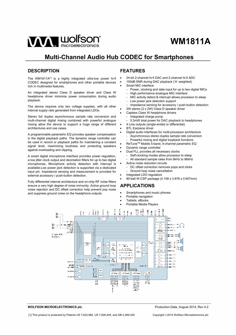
The following table identifies the power domain and ground reference associated with each of the input / output pins.
PIN NO NAME POWER DOMAIN GROUND DOMAIN
F4 ADCDAT1 DBVDD1 DGND
H4 ADCDAT2 DBVDD2 DGND
J1 ADCLRCLK1/GPIO1 DBVDD1 DGND
F3 ADDR DBVDD1 DGND
G3 BCLK1 DBVDD1 DGND
K1 BCLK2 DBVDD2 DGND
H1 DACDAT1 DBVDD1 DGND
G4 DACDAT2 DBVDD2 DGND
A8 DMICCLK MICBIAS1 AGND
K3 GPIO8/DACDAT3 DBVDD3 DGND
J4 GPIO9/ADCDAT3 DBVDD3 DGND
G5 GPIO10/LRCLK3 DBVDD3 DGND
K4 GPIO11/BCLK3 DBVDD3 DGND
J6 HPOUT1L CPVOUTP, CPVOUTN CPGND
J5 HPOUT1R CPVOUTP, CPVOUTN CPGND
G8 HPOUT2N AVDD1 HP2GND
H7 HPOUT2P AVDD1 HP2GND
D7 IN1LN AVDD1 AGND
D8 IN1LP AVDD1 AGND
B9 IN1RN AVDD1 AGND
C7 IN1RP AVDD1 AGND
C8 IN2LN/DMICDAT AVDD1 (IN2LN) or
MICBIAS1 (DMICDAT)
AGND
C9 IN2LP/VRXN AVDD1 AGND
B7 IN2RN AVDD1 AGND
B8 IN2RP/VRXP AVDD1 AGND
K2 JACKDET AVDD2 AGND
A4 LDO1ENA DBVDD1 DGND
D6 LDO2ENA DBVDD1 DGND
C6 LINEOUT1N AVDD1 AGND
B6 LINEOUT1P AVDD1 AGND
A6 LINEOUT2N AVDD1 AGND
B5 LINEOUT2P AVDD1 AGND
G1 LRCLK1 DBVDD1 DGND
J3 LRCLK2 DBVDD2 DGND
F1 MCLK1 DBVDD1 DGND
F2 MCLK2 DBVDD1 DGND
F9 MICDET MICBIAS2 AGND
H2 SCLK DBVDD1 DGND
H3 SDA DBVDD1 DGND
D5 SPKMODE DBVDD1 DGND
A1, B1 SPKOUTLN SPKVDD1 SPKGND1
B3, B4 SPKOUTLP SPKVDD1 SPKGND1
C1, D1 SPKOUTRN SPKVDD2 SPKGND2
C3, D4 SPKOUTRP SPKVDD2 SPKGND2

Production Data WM1811A
w PD, August 2014, Rev 4.2
11
ABSOLUTE MAXIMUM RATINGS
Absolute Maximum Ratings are stress ratings only. Permanent damage to the device may be caused by continuously operating at or beyond these limits. Device functional operating limits and guaranteed performance specifications are given under Electrical Characteristics at the test conditions specified.
ESD Sensitive Device. This device is manufactured on a CMOS process. It is therefore generically susceptible to damage from excessive static voltages. Proper ESD precautions must be taken during handling and storage of this device.
Wolfson tests its package types according to IPC/JEDEC J-STD-020 for Moisture Sensitivity to determine acceptable storage conditions prior to surface mount assembly. These levels are:
MSL1 = unlimited floor life at <30C / 85% Relative Humidity. Not normally stored in moisture barrier bag. MSL2 = out of bag storage for 1 year at <30C / 60% Relative Humidity. Supplied in moisture barrier bag. MSL3 = out of bag storage for 168 hours at <30C / 60% Relative Humidity. Supplied in moisture barrier bag.
The Moisture Sensitivity Level for each package type is specified in Ordering Information.
CONDITION MIN MAX
Supply voltages (AVDD1, DBVDD2, DBVDD3) -0.3V +4.5V
Supply voltages (AVDD2, DCVDD, DBVDD1) -0.3V +2.5V
Supply voltages (CPVDD) -0.3V +2.2V
Supply voltages (SPKVDD1, SPKVDD2, LDO1VDD) -0.3V +7.0V
Voltage range digital inputs (DBVDD1 domain) AGND -0.3V DBVDD1 +0.3V
Voltage range digital inputs (DBVDD2 domain) AGND -0.3V DBVDD2 +0.3V
Voltage range digital inputs (DBVDD3 domain) AGND -0.3V DBVDD3 +0.3V
Voltage range digital inputs (DMICDAT) AGND -0.3V AVDD1 +0.3V
Voltage range analogue inputs(AVDD1 domain) AGND -0.3V AVDD1 +0.3V
Voltage range analogue inputs (MICDET, LINEOUTFB) AGND -0.3V AVDD1 +0.3V
Voltage range analogue inputs (HPOUT1FB) AGND -0.3V AGND +0.3V
Voltage range analogue inputs (JACKDET)
See note 1
CPVOUTN - 0.3V AVDD2 +0.3V
Ground (DGND, CPGND, SPKGND1, SPKGND2, REFGND, HP2GND) AGND -0.3V AGND +0.3V
Operating temperature range, TA -40ºC +85ºC
Junction temperature, TJMAX -40ºC +150ºC
Storage temperature after soldering -65ºC +150ºC
Notes:
1. CPVOUTN is an internal supply rail, generated by the WM1811A Charge Pump. The CPVOUTN voltage may vary between AGND and -CPVDD.
WM1811A Production Data
w PD, August 2014, Rev 4.2
12
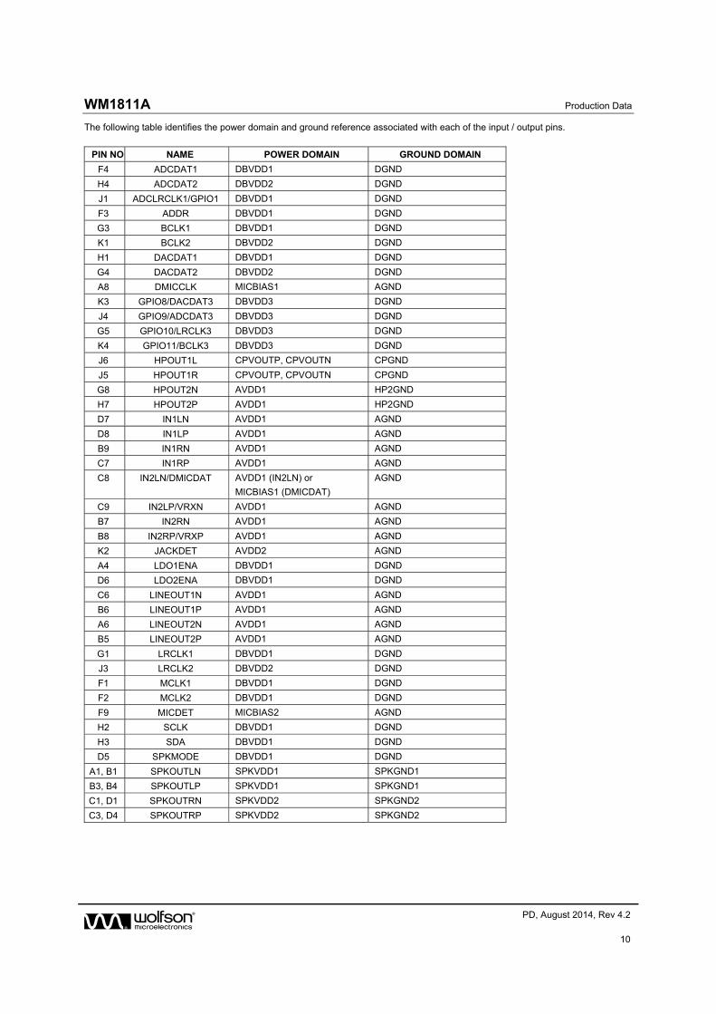
RECOMMENDED OPERATING CONDITIONS
PARAMETER SYMBOL MIN TYP MAX UNIT
Digital supply range (Core)
See notes 7, 8
DCVDD 1.00 1.05 2.0 V
Digital supply range (I/O) DBVDD1 1.62 1.8 2.0 V
Digital supply range (I/O) DBVDD2, DBVDD3 1.62 1.8 3.6 V
Analogue supply 1 range
See notes 3, 4, 5, 6
AVDD1 2.4 3.0 3.3 V
Analogue supply 2 range AVDD2 1.71 1.8 2.0 V
Charge Pump supply range CPVDD 1.71 1.8 2.0 V
Speaker supply range SPKVDD1, SPKVDD2 2.7 5.0 5.5 V
LDO1 supply range LDO1VDD 2.7 5.0 5.5 V
Ground DGND, AGND, CPGND, SPKGND1, SPKGND2,
REFGND, HP2GND
0 V
Power supply rise time
See notes 9, 10, 11
All supplies 1 s
Operating temperature range TA -40 85 °C
Notes:
1. Analogue, digital and speaker grounds must always be within 0.3V of AGND.
2. There is no power sequencing requirement; the supplies may be enabled in any order.
3. AVDD1 must be less than or equal to SPKVDD1 and SPKVDD2.
4. An internal LDO (powered by LDO1VDD) can be used to provide the AVDD1 supply.
5. When AVDD1 is supplied externally (not from LDO1), the LDO1VDD voltage must be greater than or equal to AVDD1.
6. The WM1811A can operate with AVDD1 tied to 0V; power consumption may be reduced, but the analogue audio functions will not be supported.
7. An internal LDO (powered by DBVDD1) can be used to provide the DCVDD supply.
8. When DCVDD is supplied externally (not from LDO2), the DBVDD1voltage must be greater than or equal to DCVDD.
9. DCVDD and AVDD1 minimum rise times do not apply when these domains are powered using the internal LDOs.
10. The specified minimum power supply rise times assume a minimum decoupling capacitance of 100nF per pin. However, Wolfson strongly advises that the recommended decoupling capacitors are present on the PCB and that appropriate layout guidelines are observed (see “Applications Information” section).
11. The specified minimum power supply rise times also assume a maximum PCB inductance of 10nH between decoupling capacitor and pin.

Production Data WM1811A
w PD, August 2014, Rev 4.2
13
ELECTRICAL CHARACTERISTICS
INPUT SIGNAL LEVEL
Test Conditions
AVDD1 = 3.0V. With the exception of the condition(s) noted above, the following electrical characteristics are valid across the full range of recommended operating conditions.
PARAMETER TEST CONDITIONS MIN TYP MAX UNIT
A1 Full-Scale PGA Input Signal Level
See notes 1, 2, 3 and 4
Single-ended PGA input 1.0
0
Vrms
dBV
Differential PGA input 1.0
0
Vrms
dBV
A2 Full-Scale Line Input Signal Level
See notes 1, 2, 3 and 4
Single-ended Line input toMIXINL/R, SPKMIXL/R or
MIXOUTL/R mixers
1.0
0
Vrms
dBV
Differential mono line input on VRXP/VRXN to
RXVOICE
1.0
0
Vrms
dBV
Notes:
1. The full-scale input signal level changes in proportion with AVDD1. It is calculated as AVDD1/3.0.
2. When mixing line inputs, input PGA outputs and DAC outputs the total signal must not exceed 1.0Vrms (0dBV).
3. A 1.0Vrms differential signal equates to 0.5Vrms/-6dBV per input.
4. A sinusoidal input signal is assumed.

WM1811A Production Data
w PD, August 2014, Rev 4.2
14
INPUT PIN RESISTANCE
Test Conditions
TA = +25oC. With the exception of the condition(s) noted above, the following electrical characteristics are valid across the full range of recommended operating conditions.
PARAMETER TEST CONDITIONS MIN TYP MAX UNIT
B1 PGA Input Resistance Differential Mode
See note 5
See “Applications Information” for details of Input resistance at all PGA Gain settings.
Gain = -16.5dB
(INnx_VOL=00h)
53 k
Gain = 0dB
(INnx_VOL=0Bh)
25 k
Gain = +30dB
(INnx_VOL=1Fh)
1.3 k
B2 PGA Input Resistance Single-Ended Mode
See note 5
See “Applications Information” for details of Input resistance at all PGA Gain settings.
Gain = -16.5dB
(INnx_VOL=00h)
58 k
Gain = 0dB
(INnx_VOL=0Bh)
36 k
Gain = +30dB
(INnx_VOL=1Fh)
2.5 k
B3 Line Input Resistance
See note 5
IN1LP to MIXINL, or IN1RP to MIXINR
Gain = -12dB
(IN1xP_MIXINx_VOL=001)
56 k
IN1LP to MIXINL, or IN1RP to MIXINR
Gain = 0dB
(IN1xP_MIXINx_VOL=101)
18 k
IN1LP to MIXINL, or IN1RP to MIXINR
Gain = +6dB
(IN1xP_MIXINx_VOL=111)
9.8 k
IN1LP to MIXINL, or IN1RP to MIXINR
Gain = +15dB
(IN1xP_MIXINx_VOL=111, IN1xP_MIXINx_BOOST=1)
3.7 k
IN1LPto SPKMIXL, or IN1RP to SPKMIXR
(SPKATTN = -12dB)
89 k
IN1LPto SPKMIXL, or IN1RP to SPKMIXR
(SPKATTN = 0dB)
27 k
IN2LN, IN2RN, IN2LP or IN2RP to MIXOUTL or
MIXOUTR
Gain = -9dB
(*MIXOUTx_VOL=011)
43 k
IN2LN,IN2RN, IN2LP or IN2RP to MIXOUTL or
MIXOUTR
Gain = 0dB
18 k

Production Data WM1811A
w PD, August 2014, Rev 4.2
15
Test Conditions
TA = +25oC. With the exception of the condition(s) noted above, the following electrical characteristics are valid across the full range of recommended operating conditions.
PARAMETER TEST CONDITIONS MIN TYP MAX UNIT
(*MIXOUTx_VOL=000)
RXVOICE to MIXINLorMIXINR
Gain = -12dB
(IN2LRP_MIXINx_VOL=001)
48 k
RXVOICE to MIXINLorMIXINR
Gain = 0dB
(IN2LRP_MIXINx_VOL=101)
12 k
RXVOICE to MIXINLorMIXINR
Gain = +6dB
(IN2LRP_MIXINx_VOL=111)
6.0 k
Note 5: Input resistance will be seen in parallel with the resistance of other enabled input paths from the same pins

WM1811A Production Data
w PD, August 2014, Rev 4.2
16
PROGRAMMABLE GAINS
Test Conditions
The following electrical characteristics are valid across the full range of recommended operating conditions.
PARAMETER TEST CONDITIONS MIN TYP MAX UNIT
Input PGAs (IN1L, IN2L, IN1R and IN2R)
C1 Minimum Programmable Gain Guaranteed monotonic -16.5 dB
C2 Maximum Programmable Gain +30 dB
C3 Programmable Gain Step Size 1.5 dB
Input Mixers (MIXINL and MIXINR)
C6 Minimum Programmable Gain Input PGA signal paths 0 dB
C7 Maximum Programmable Gain +30 dB
C8 Programmable Gain Step Size 30 dB
C9 Minimum Programmable Gain Direct IN1xP input signal paths
(Note the available gain settings are -12, -9, -6, -3, 0, +3, +6, +15dB)
-12 dB
C10 Maximum Programmable Gain +15 dB
C11 Programmable Gain Step Size 3 dB
Minimum Programmable Gain MIXOUTx Record signal paths -12 dB
Maximum Programmable Gain +6 dB
Programmable Gain Step Size 3 dB
C12 Minimum Programmable Gain RXVOICE (VRXP-VRXN) signal paths -12 dB
C13 Maximum Programmable Gain +6 dB
C14 Programmable Gain Step Size 3 dB
Output Mixers (MIXOUTL and MIXOUTR)
C17 Minimum Programmable Gain -9 dB
C18 Maximum Programmable Gain 0 dB
C19 Programmable Gain Step Size 3 dB
Speaker Mixers (SPKMIXL and SPKMIXR)
C21 Minimum Programmable Gain -6 dB
C22 Maximum Programmable Gain 0 dB
C23 Programmable Gain Step Size 6 dB
Output PGAs (HPOUT1LVOL, HPOUT1RVOL, MIXOUTLVOL, MIXOUTRVOL, SPKLVOL and SPKRVOL)
C25 Minimum Programmable Gain Guaranteed monotonic -57 dB
C26 Maximum Programmable Gain +6 dB
C27 Programmable Gain Step Size 1 dB
Line Output Drivers (LINEOUT1NMIX, LINEOUT1PMIX, LINEOUT2NMIX and LINEOUT2PMIX)
C29 Minimum Programmable Gain -6 dB
C30 Maximum Programmable Gain 0 dB
C31 Programmable Gain Step Size 6 dB
EarpieceDriver (HPOUT2MIX)
C33 Minimum Programmable Gain -6 dB
C34 Maximum Programmable Gain 0 dB
C35 Programmable Gain Step Size 6 dB
Speaker Output Drivers (SPKOUTLBOOST and SPKOUTRBOOST)
C38 Minimum Programmable Gain (Note the available gain settings are 0, +1.5, +3, +4.5, +6, +7.5, +9, +12dB)
0 dB
C39 Maximum Programmable Gain +12 dB
C40 Programmable Gain Step Size 1.5 dB
Production Data WM1811A
w PD, August 2014, Rev 4.2
17
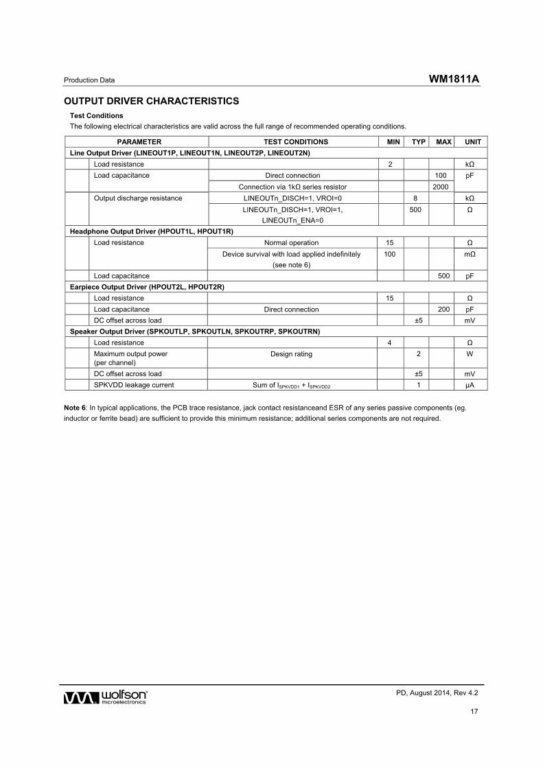
OUTPUT DRIVER CHARACTERISTICS
Test Conditions
The following electrical characteristics are valid across the full range of recommended operating conditions.
PARAMETER TEST CONDITIONS MIN TYP MAX UNIT
Line Output Driver (LINEOUT1P, LINEOUT1N, LINEOUT2P, LINEOUT2N)
Load resistance 2 kΩ
Load capacitance Direct connection 100 pF
Connection via 1kΩ series resistor 2000
Output discharge resistance LINEOUTn_DISCH=1, VROI=0 8 kΩ
LINEOUTn_DISCH=1, VROI=1,
LINEOUTn_ENA=0
500 Ω
Headphone Output Driver (HPOUT1L, HPOUT1R)
Load resistance Normal operation 15 Ω
Device survival with load applied indefinitely
(see note 6)
100 mΩ
Load capacitance 500 pF
Earpiece Output Driver (HPOUT2L, HPOUT2R)
Load resistance 15 Ω
Load capacitance Direct connection 200 pF
DC offset across load ±5 mV
Speaker Output Driver (SPKOUTLP, SPKOUTLN, SPKOUTRP, SPKOUTRN)
Load resistance 4 Ω
Maximum output power (per channel)
Design rating 2 W
DC offset across load ±5 mV
SPKVDD leakage current Sum of ISPKVDD1 + ISPKVDD2 1 µA
Note 6: In typical applications, the PCB trace resistance, jack contact resistanceand ESR of any series passive components (eg.
inductor or ferrite bead) are sufficient to provide this minimum resistance; additional series components are not required.

WM1811A Production Data
w PD, August 2014, Rev 4.2
18
ADC INPUT PATH PERFORMANCE
Test Conditions
AVDD1=3.0V (powered from LDO1), DCVDD=1.05V (powered from LDO2), AVDD2=DBVDD1=DBVDD2=DBVDD3=CPVDD=1.8V, LDO1VDD=SPKVDD1=SPKVDD2=5V, DGND=AGND=CPGND=SPKGND1=SPKGND2=HP2GND=0V, TA = +25oC, 1kHz sinusoidal signal, fs = 48kHz, PGA gain = 0dB, 24-bit audio data unless otherwise stated.
PARAMETER TEST CONDITIONS MIN TYP MAX UNIT
D1 Line Inputs to ADC via MIXINL and MIXINR
SNR A-weighted
94 dB
THD -1dBV input -83 dB
THD+N -1dBV input -81 dB
Channel Separation (L/R)
-100 dB
PSRR (SPKVDDn, LDO1VDD)
100mV (pk-pk) 217Hz
92 dB
PSRR (AVDD2, CPVDD, DBVDDn)
100mV (pk-pk) 217Hz
94 dB
D2 Record Path (DACs to ADCs via MIXINL and MIXINR)
SNR A-weighted 92 dB
THD -1dBFS input -74 dB
THD+N -1dBFS input -72 dB
Channel Separation (L/R)
-95 dB
PSRR (SPKVDDn, LDO1VDD)
100mV (pk-pk) 217Hz
97 dB
PSRR (AVDD2, CPVDD, DBVDDn)
100mV (pk-pk) 217Hz
94 dB
D3 Input PGAs to ADC via MIXINL or MIXINR
SNR A-weighted -
+
0dB MIXINL or MIXINR
IN1L, IN2L, IN1R or IN2R
(Single-ended or differential mode)
IN1LN, IN2LN, IN1RN or IN2RN
IN1LP, IN2LP, IN1RP or IN2RP
+ ADCL or ADCR
84 95 dB
THD -1dBV input -82 -72 dB
THD+N -1dBV input -80 -70 dB
Channel Separation (L/R)
-100 dB
PSRR (SPKVDDn, LDO1VDD)
100mV (pk-pk) 217Hz
100 dB
PSRR (AVDD2, CPVDD, DBVDDn)
100mV (pk-pk) 217Hz
95 dB
CMRR Input PGA=-16.5dB1V (pk-pk) 217Hz
49 dB
Input PGA = 0dB1V (pk-pk) 217Hz
58
Input PGA = +30dB1V (pk-pk) 217Hz
73
Note that the Input PGA gain is controlled using the INnx_VOL registers.

Production Data WM1811A
w PD, August 2014, Rev 4.2
19
Test Conditions
AVDD1=3.0V (powered from LDO1), DCVDD=1.05V (powered from LDO2), AVDD2=DBVDD1=DBVDD2=DBVDD3=CPVDD=1.8V, LDO1VDD=SPKVDD1=SPKVDD2=5V, DGND=AGND=CPGND=SPKGND1=SPKGND2=HP2GND=0V, TA = +25oC, 1kHz sinusoidal signal, fs = 48kHz, PGA gain = 0dB, 24-bit audio data unless otherwise stated.
PARAMETER TEST CONDITIONS MIN TYP MAX UNIT
D4 RXVOICE to ADCL or ADCR
SNR A-weighted
94 dB
THD -1dBV input -84 dB
THD+N -1dBV input -82 dB
PSRR (SPKVDDn, LDO1VDD)
100mV (pk-pk) 217Hz
102 dB
PSRR (AVDD2, CPVDD, DBVDDn)
100mV (pk-pk) 217Hz
97 dB
CMRR Input PGA = -12dB1V (pk-pk) 217Hz
56 dB
Input PGA = 0dB1V (pk-pk) 217Hz
63
Input PGA = +6dB1V (pk-pk) 217Hz
61
Note that the Input PGA gain is controlled using the IN2LRP_MIXINx_VOL registers.
DAC OUTPUT PATH PERFORMANCE
Test Conditions
AVDD1=3.0V (powered from LDO1), DCVDD=1.05V (powered from LDO2), AVDD2=DBVDD1=DBVDD2=DBVDD3=CPVDD=1.8V, LDO1VDD=SPKVDD1=SPKVDD2=5V, DGND=AGND=CPGND=SPKGND1=SPKGND2=HP2GND=0V, TA = +25oC, 1kHz sinusoidal signal, fs = 48kHz, PGA gain = 0dB, 24-bit audio data unless otherwise stated.
PARAMETER TEST CONDITIONS MIN TYP MAX UNIT
E1 DAC to Single-Ended Line Output (Load = 10k // 50pF)
SNR A-weighted 93 dB
THD 0dBFS input -82 dB
THD+N 0dBFS input -80 dB
Channel Separation (L/R)
-90 dB
PSRR (SPKVDDn, LDO1VDD)
100mV (pk-pk) 217Hz
85 dB
PSRR (AVDD2, CPVDD, DBVDDn)
100mV (pk-pk) 217Hz
95 dB
LINEOUTFB rejection LINEOUTn_FB=1, 100mV (pk-pk)
217Hz
38 dB
E2 DAC to Differential Line Output (Load = 10k // 50pF)
SNR A-weighted
97 dB
THD 0dBFS input -82 dB
THD+N 0dBFS input -80 dB
Channel Separation (L/R)
-90 dB
PSRR (SPKVDDn, LDO1VDD)
100mV (pk-pk) 217Hz
87 dB
PSRR (AVDD2, CPVDD, DBVDDn)
100mV (pk-pk) 217Hz
88 dB

WM1811A Production Data
w PD, August 2014, Rev 4.2
20
Test Conditions
AVDD1=3.0V (powered from LDO1), DCVDD=1.05V (powered from LDO2), AVDD2=DBVDD1=DBVDD2=DBVDD3=CPVDD=1.8V, LDO1VDD=SPKVDD1=SPKVDD2=5V, DGND=AGND=CPGND=SPKGND1=SPKGND2=HP2GND=0V, TA = +25oC, 1kHz sinusoidal signal, fs = 48kHz, PGA gain = 0dB, 24-bit audio data unless otherwise stated.
PARAMETER TEST CONDITIONS MIN TYP MAX UNIT
E5 DAC to Headphone on HPOUT1L or HPOUT1R (Load = 32)
SNR (A-weighted) DAC_OSR128=1
100 dB
DAC_OSR128=0 97 dB
THD PO=20mW -74 dB
THD+N PO=20mW -72 dB
THD PO=5mW -76 dB
THD+N PO=5mW -74 dB
Channel Separation (L/R)
-95 dB
PSRR (SPKVDDn, LDO1VDD)
100mV (pk-pk) 217Hz
96 dB
PSRR (AVDD2, CPVDD, DBVDDn)
100mV (pk-pk) 217Hz
89 dB
HPOUT1FB rejection 100mV (pk-pk) 217Hz
29 dB
E6 DAC to Headphone on HPOUT1L or HPOUT1R (Load = 16)
SNR (A-weighted) DAC_OSR128=1
90 100 dB
DAC_OSR128=0 97 dB
THD PO=20mW -82 dB
THD+N PO=20mW -80 dB
THD PO=5mW -83 -73 dB
THD+N PO=5mW -81 -71 dB
Channel Separation (L/R)
-95 dB
PSRR (SPKVDDn, LDO1VDD)
100mV (pk-pk) 217Hz
98 dB
PSRR (AVDD2, CPVDD, DBVDDn)
100mV (pk-pk) 217Hz
88 dB
HPOUT1FB rejection 100mV (pk-pk) 217Hz
29 dB
E9 DAC to Earpiece Driver (Load = 16 BTL)
SNR A-weighted
97 dB
THD PO=50mW -71 dB
THD+N PO=50mW -69 dB
PSRR (SPKVDDn, LDO1VDD)
100mV (pk-pk) 217Hz
95 dB
PSRR (AVDD2, CPVDD, DBVDDn)
100mV (pk-pk) 217Hz
96 dB

Production Data WM1811A
w PD, August 2014, Rev 4.2
21
Test Conditions
AVDD1=3.0V (powered from LDO1), DCVDD=1.05V (powered from LDO2), AVDD2=DBVDD1=DBVDD2=DBVDD3=CPVDD=1.8V, LDO1VDD=SPKVDD1=SPKVDD2=5V, DGND=AGND=CPGND=SPKGND1=SPKGND2=HP2GND=0V, TA = +25oC, 1kHz sinusoidal signal, fs = 48kHz, PGA gain = 0dB, 24-bit audio data unless otherwise stated.
PARAMETER TEST CONDITIONS MIN TYP MAX UNIT
E12 DAC to Speaker Outputs (Load = 8 + 22H BTL, Stereo Mode)
+12dB boost (SPKOUTx_BOOST = 111)
SNR A-weighted
SPKMIXL or SPKMIXR
+DACLorDACR
+
SPKLVOL or SPKRVOL
SPKOUTLBOOST or
SPKOUTRBOOST
RLOAD=
8ohm
SPKOUTLP orSPKOUTRP
SPKOUTLN orSPKOUTRN
+12dB
85 94 dB
THD PO=0.5W -65 dB
THD+N PO=0.5W -63 -53 dB
THD PO=1.0W -70 dB
THD+N PO=1.0W -68 dB
Channel Separation (L/R)
-80 dB
PSRR (SPKVDDn, LDO1VDD)
100mV (pk-pk) 217Hz
72 dB
PSRR (AVDD2, CPVDD, DBVDDn)
100mV (pk-pk) 217Hz
78 dB
BYPASS PATH PERFORMANCE
Test Conditions
AVDD1=3.0V (powered from LDO1), DCVDD=1.05V (powered from LDO2), AVDD2=DBVDD1=DBVDD2=DBVDD3=CPVDD=1.8V, LDO1VDD=SPKVDD1=SPKVDD2=5V, DGND=AGND=CPGND=SPKGND1=SPKGND2=HP2GND=0V, TA = +25oC, 1kHz sinusoidal signal, fs = 48kHz, PGA gain = 0dB, 24-bit audio data unless otherwise stated.
PARAMETER TEST CONDITIONS MIN TYP MAX UNIT
F1 Input PGA to Differential Line Output (Load = 10k // 50pF)
SNR A-weighted
100 dB
THD 0dBV output -90 dB
THD+N 0dBV output -87 dB
PSRR (SPKVDDn, LDO1VDD)
100mV (pk-pk) 217Hz
90 dB
PSRR (AVDD2, CPVDD, DBVDDn)
100mV (pk-pk) 217Hz
90 dB
CMRR Input PGA = 0dB1V (pk-pk) 217Hz
58 dB
Note that the Input PGA gain is controlled using the INnx_VOL registers.
F3 Input PGA to Headphone via MIXOUTL or MIXOUTR (Load = 16)
SNR A-weighted 98 dB
THD PO=20mW -89 dB
THD+N PO=20mW -87 dB
THD PO=5mW -86 dB
THD+N PO=5mW -84 dB
Channel Separation (L/R)
-95 dB
PSRR (SPKVDDn, LDO1VDD)
100mV (pk-pk) 217Hz
100 dB
PSRR (AVDD2, CPVDD, DBVDDn)
100mV (pk-pk) 217Hz
89 dB
CMRR Input PGA = 0dB1V (pk-pk) 217Hz
58 dB
Note that the Input PGA gain is controlled using the INnx_VOL registers.

WM1811A Production Data
w PD, August 2014, Rev 4.2
22
Test Conditions
AVDD1=3.0V (powered from LDO1), DCVDD=1.05V (powered from LDO2), AVDD2=DBVDD1=DBVDD2=DBVDD3=CPVDD=1.8V, LDO1VDD=SPKVDD1=SPKVDD2=5V, DGND=AGND=CPGND=SPKGND1=SPKGND2=HP2GND=0V, TA = +25oC, 1kHz sinusoidal signal, fs = 48kHz, PGA gain = 0dB, 24-bit audio data unless otherwise stated.
PARAMETER TEST CONDITIONS MIN TYP MAX UNIT
F2 Line Input (IN2LP or IN2RP) to Headphone via MIXOUTL or MIXOUTR (Load = 16)
SNR A-weighted
100 dB
THD PO=20mW -86 dB
THD+N PO=20mW -84 dB
THD PO=5mW -84 dB
THD+N PO=5mW -82 dB
PSRR (SPKVDDn, LDO1VDD)
100mV (pk-pk) 217Hz
93 dB
PSRR (AVDD2, CPVDD, DBVDDn)
100mV (pk-pk) 217Hz
87 dB
F4 Line Input (IN2LN or IN2RN) to Headphone via MIXOUTL or MIXOUTR (Load = 16)
SNR A-weighted
100 dB
THD PO=20mW -84 dB
THD+N PO=20mW -82 dB
THD PO=5mW -82 dB
THD+N PO=5mW -80 dB
Channel Separation (L/R)
-95 dB
PSRR (SPKVDDn, LDO1VDD)
100mV (pk-pk) 217Hz
94 dB
PSRR (AVDD2, CPVDD, DBVDDn)
100mV (pk-pk) 217Hz
87 dB
F8 Line Input to Speaker Outputs via SPKMIXL or SPKMIXR (Load = 8 + 22HBTL, Stereo Mode)
+12dB boost (SPKOUTx_BOOST = 111)
SNR A-weighted 93 dB
THD PO=0.5W -62 dB
THD+N PO=0.5W -60 dB
THD PO=1.0W -67 dB
THD+N PO=1.0W -65 dB
PSRR (SPKVDDn, LDO1VDD)
100mV (pk-pk) 217Hz
68 dB
PSRR (AVDD2, CPVDD, DBVDDn)
100mV (pk-pk) 217Hz
76 dB

Production Data WM1811A
w PD, August 2014, Rev 4.2
23
MULTI-PATH CROSSTALK
Test Conditions
AVDD1=3.0V (powered from LDO1), DCVDD=1.05V (powered from LDO2), AVDD2=DBVDD1=DBVDD2=DBVDD3=CPVDD=1.8V, LDO1VDD=SPKVDD1=SPKVDD2=5V, DGND=AGND=CPGND=SPKGND1=SPKGND2=HP2GND=0V, TA = +25oC, 1kHz sinusoidal signal, fs = 48kHz, PGA gain = 0dB, 24-bit audio data unless otherwise stated.
PARAMETER TEST CONDITIONS MIN TYP MAX UNIT
G1 Headset Voice Call:
DAC/Headset to Tx Voice Separation
1kHz 0dBFS DAC playback direct to HPOUT1L and HPOUT1R; Quiescent input on IN1LN/P or IN1RN/P (Gain=+12dB), differential line output; Measure crosstalk at differential line output
85 dB
G2 Speakerphone Voice Call:
DAC/Speaker to Tx Voice Separation
1kHz 0dBFS DAC playback to speakers, 1W/chan output; Quiescent input on IN1LN/P or IN1RN/P (Gain=+12dB), differential line output; Measure crosstalk at differential line output
100 dB
G3 Earpiece PCM Voice Call:
RXVOICE to Tx Voice Separation
fs=8kHz for ADC and DAC, DAC_SB_FILT=1; -5dBFS, DAC output to HPOUT2P-HPOUT2N; Quiescent input on input PGA (Gain=+12dB) to ADC via MIXINL or MIXINR; Measure crosstalk at ADC output
110 dB
G4 Speakerphone PCM Voice Call:
DAC/Speaker to ADC Separation
fs=8kHz for ADC and DAC, DAC_SB_FILT=1; 0dBFS DAC output to speaker (1W output); ADC record from input PGA (Gain=+30dB); Measure crosstalk on ADC output
+
MIXINL or MIXINR
ADCL or ADCR
CROSSTALK
-
+
+30dB
IN1L, IN2L, IN1R or IN2R
Quiescent input
IN1LN, IN2LN, IN1RN or IN2RN
IN1LP, IN2LP, IN1RP or IN2RP
+SPKMIXL
DACLRLOAD =
8Ohm
0dB
SPKOUTLP
SPKOUTLN
0dB
SPKLVOL
+SPKMIXR
RLOAD = 8Ohm
0dB
SPKOUTRP
SPKOUTRN
0dB
SPKRVOL
DACR
90 dB
G5 Speakerphone PCM Voice Call:
ADC to DAC/Speaker Separation
fs=8kHz for ADC and DAC, DAC_SB_FILT=1; Quiescent DAC output to speaker; ADC record from input PGA (Gain=+30dB + 30dB boost); Measure crosstalk on speaker output
+
MIXINL or MIXINR
ADCL or ADCR
-
+
+30dB
IN1L, IN2L, IN1R or IN2R
1kHz input
IN1LN, IN2LN, IN1RN or IN2RN
IN1LP, IN2LP, IN1RP or IN2RP
+SPKMIXL
DACLRLOAD =
8Ohm
0dB
SPKOUTLP or SPKOUTRP
SPKOUTLN or SPKOUTRN
0dB
SPKLVOL
+30dB gain
CROSSTALK
95 dB

WM1811A Production Data
w PD, August 2014, Rev 4.2
24
Test Conditions
AVDD1=3.0V (powered from LDO1), DCVDD=1.05V (powered from LDO2), AVDD2=DBVDD1=DBVDD2=DBVDD3=CPVDD=1.8V, LDO1VDD=SPKVDD1=SPKVDD2=5V, DGND=AGND=CPGND=SPKGND1=SPKGND2=HP2GND=0V, TA = +25oC, 1kHz sinusoidal signal, fs = 48kHz, PGA gain = 0dB, 24-bit audio data unless otherwise stated.
PARAMETER TEST CONDITIONS MIN TYP MAX UNIT
G6 Earpiece Speaker Voice Call:
Tx Voice and RXVOICE Separation
1kHz Full scale differential input on VRXP-VRXN, output to HPOUT2P-HPOUT2N; Quiescent input on IN1LN/P or IN1RN/P (Gain=+12dB), differential line output; Measure crosstalk at differential line output
100 dB
G7 Headset Voice Call:
Tx Voice and RXVOICE Separation
1kHz full scale differential input on VRXP-VRXN via RXVOICE to MIXOUTL and MIXOUTR, output to HPOUT1L and HPOUT1R; Quiescent input on IN1LN/P or IN1RN/P (Gain=+12dB), differential line output; Measure crosstalk at differential line output
CR
OS
STA
LK
90 dB
G8 Stereo Line Record and Playback:
DAC/Headset to ADC Separation
-5dBFS input to DACs, playback to HPOUT1L and HPOUT1R; ADC record from line input; Measure crosstalk on ADC output
DACR
HPOUT1LVOL
0dB
DACL
HPOUT1RVOL
0dB
+
MIXINL or MIXINR
ADCL or ADCR
CROSSTALK
Quiescent input
HPOUT1L
HPOUT1R
IN1LP or IN1RP
95 dB
Production Data WM1811A
w PD, August 2014, Rev 4.2
25
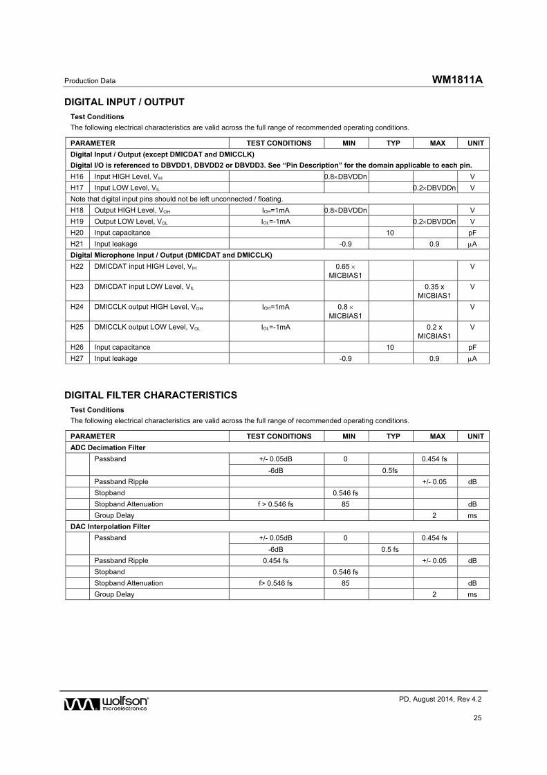
DIGITAL INPUT / OUTPUT
Test Conditions
The following electrical characteristics are valid across the full range of recommended operating conditions.
PARAMETER TEST CONDITIONS MIN TYP MAX UNIT
Digital Input / Output (except DMICDAT and DMICCLK)
Digital I/O is referenced to DBVDD1, DBVDD2 or DBVDD3. See “Pin Description” for the domain applicable to each pin.
H16 Input HIGH Level, VIH 0.8DBVDDn V
H17 Input LOW Level, VIL 0.2DBVDDn V
Note that digital input pins should not be left unconnected / floating.
H18 Output HIGH Level, VOH IOH=1mA 0.8DBVDDn V
H19 Output LOW Level, VOL IOL=-1mA 0.2DBVDDn V
H20 Input capacitance 10 pF
H21 Input leakage -0.9 0.9 A
Digital Microphone Input / Output (DMICDAT and DMICCLK)
H22 DMICDAT input HIGH Level, VIH 0.65 MICBIAS1
V
H23 DMICDAT input LOW Level, VIL 0.35 x MICBIAS1
V
H24 DMICCLK output HIGH Level, VOH IOH=1mA 0.8 MICBIAS1
V
H25 DMICCLK output LOW Level, VOL IOL=-1mA 0.2 x MICBIAS1
V
H26 Input capacitance 10 pF
H27 Input leakage -0.9 0.9 A
DIGITAL FILTER CHARACTERISTICS
Test Conditions
The following electrical characteristics are valid across the full range of recommended operating conditions.
PARAMETER TEST CONDITIONS MIN TYP MAX UNIT
ADC Decimation Filter
Passband +/- 0.05dB 0 0.454 fs
-6dB 0.5fs
Passband Ripple +/- 0.05 dB
Stopband 0.546 fs
Stopband Attenuation f > 0.546 fs 85 dB
Group Delay 2 ms
DAC Interpolation Filter
Passband +/- 0.05dB 0 0.454 fs
-6dB 0.5 fs
Passband Ripple 0.454 fs +/- 0.05 dB
Stopband 0.546 fs
Stopband Attenuation f> 0.546 fs 85 dB
Group Delay 2 ms

WM1811A Production Data
w PD, August 2014, Rev 4.2
26
MICROPHONE BIAS CHARACTERISTICS
Test Conditions
AVDD1=3.0V (powered from LDO1), DCVDD=1.05V (powered from LDO2), AVDD2=DBVDD1=DBVDD2=DBVDD3=CPVDD=1.8V, LDO1VDD=SPKVDD1=SPKVDD2=5V, DGND=AGND=CPGND=SPKGND1=SPKGND2=HP2GND=0V, TA = +25oC, unless otherwise stated.
PARAMETER TEST CONDITIONS MIN TYP MAX UNIT
Microphone Bias (MICBIAS1 and MICBIAS2)
Note - No capacitor on MICBIASn
Note - In regulator mode, it is required that AVDD1 - VMICBIASn> 200mV
H2 Bias Voltage
Regulator mode (MICBn_MODE=0)
Load current ≤ 1.0mA
MICBn_LVL = 000 -5% 1.5 +5% V
MICBn_LVL = 001 -5% 1.8 +5%
MICBn_LVL = 010 -5% 1.9 +5%
MICBn_LVL = 011 -5% 2.0 +5%
MICBn_LVL = 100 -5% 2.2 +5%
MICBn_LVL = 101 -5% 2.4 +5%
MICBn_LVL = 110 -5% 2.5 +5%
MICBn_LVL = 111 -5% 2.6 +5%
Bias Voltage
Bypass mode (MICBn_MODE=1)
Load current ≤ 3.6mA
AVDD1 - 80mV
AVDD1 V
H3 Bias Current Regulator mode (MICBn_MODE=0)
2.4 mA
Bypass mode (MICBn_MODE=1)
3.6
H4 Output Noise Density Regulator mode (MICBn_MODE=0), MICBn_LVL = 100,
Load current = 1mA, Measured at 1kHz
60 nV/Hz
H5 Integrated Noise Voltage Regulator mode (MICBn_MODE=0), MICBn_LVL = 100,
Load current = 1mA, 100Hz to 7kHz, A-weighted
4.5 µVRMS
H6 PSRR (AVDD1)
100mV (pk-pk) 217Hz
MICBn_LVL = 000 79 dB
MICBn_LVL = 001 73
MICBn_LVL = 010 71
MICBn_LVL = 011 70
MICBn_LVL = 100 68
MICBn_LVL = 101 65
MICBn_LVL = 110 62
MICBn_LVL = 111 62
PSRR (AVDD2, CPVDD, DBVDDn)
100mV (pk-pk) 217Hz
MICBn_LVL = 000 95 dB
MICBn_LVL = 001 95
MICBn_LVL = 010 95
MICBn_LVL = 011 97
MICBn_LVL = 100 95
MICBn_LVL = 101 95
MICBn_LVL = 110 94
MICBn_LVL = 111 92
Load capacitance Regulator mode (MICBn_MODE=0)
50 pF
Output discharge resistance MICBn_ENA=0, MICBn_DISCH=1
20 kΩ

Production Data WM1811A
w PD, August 2014, Rev 4.2
27
MISCELLANEOUS CHARACTERISTICS
Test Conditions
AVDD1=3.0V (powered from LDO1), DCVDD=1.05V (powered from LDO2), AVDD2=DBVDD1=DBVDD2=DBVDD3=CPVDD=1.8V, LDO1VDD=SPKVDD1=SPKVDD2=5V, DGND=AGND=CPGND=SPKGND1=SPKGND2=HP2GND=0V, TA = +25oC, 1kHz sinusoidal signal, fs = 48kHz, PGA gain = 0dB, 24-bit audio data unless otherwise stated.
PARAMETER TEST CONDITIONS MIN TYP MAX UNIT
Analogue Reference Levels
H1 VMID Midrail Reference Voltage VMID_SEL = 01, 4.7F capacitor on VMIDC
-3% AVDD1/2 +3% V
VMID Start-Up time VMID_SEL = 01, VMID_RAMP = 11,
4.7F capacitor on VMIDC
50 ms
External Accessory Detection
Load impedance detection range
(MICDET)
2.2kΩ (2%) MICBIAS2 resistor.
Note these characteristics assume no other component is connected to MICDET. See “Applications Information” for recommended external components when a typical microphone is present.
for MICD_LVL[0] = 1 0 3 Ω
for MICD_LVL[1] = 1 13.33 15.27
for MICD_LVL[2] = 1 27.16 30.96
for MICD_LVL[3] = 1 42.48 49.47
for MICD_LVL[4] = 1 65 85
for MICD_LVL[5] = 1 114 155.24
for MICD_LVL[6] = 1 191 329.87
for MICD_LVL[7] = 1 475 30000
Jack Detection input threshold voltage
(JACKDET)
Jack insertion 0.5 x AVDD2
V
Jack removal 0.85 x AVDD2
Frequency Locked Loops (FLLs)
H29 Lock time FREF=32kHz, FOUT=12.288MHz
2.5 ms
FREF=12MHz, FOUT=12.288MHz
300 s
H30 Free-running mode start-up time 100 s
H31 Free-running mode frequency accuracy Reference supplied initially +/-10 %
No reference provided +/-30 %

WM1811A Production Data
w PD, August 2014, Rev 4.2
28
Test Conditions
AVDD1=3.0V (powered from LDO1), DCVDD=1.05V (powered from LDO2), AVDD2=DBVDD1=DBVDD2=DBVDD3=CPVDD=1.8V, LDO1VDD=SPKVDD1=SPKVDD2=5V, DGND=AGND=CPGND=SPKGND1=SPKGND2=HP2GND=0V, TA = +25oC, 1kHz sinusoidal signal, fs = 48kHz, PGA gain = 0dB, 24-bit audio data unless otherwise stated.
PARAMETER TEST CONDITIONS MIN TYP MAX UNIT
LDO Regulators
H38 LDO1 Start-Up Time 4.7F capacitor on AVDD11F capacitor on VREFC
1.5 ms
LDO1 Drop-Out voltage (LDO1VDD - AVDD1)
300 mV
LDO1 PSRR (SPKVDD, LDO1VDD) 100mV (pk-pk) 217Hz, All LDO1 output settings
50 dB
LDO1 PSRR
(AVDD2, CPVDD, DBVDDn)
100mV (pk-pk) 217Hz, All LDO1 output settings
82 dB
H42 LDO2 Start-Up Time 1F capacitor on DCVDD 1F capacitor on VREFC
1.5 ms
LDO2 PSRR (SPKVDD, LDO1VDD)
100mV (pk-pk) 217Hz
LDO2_VSEL = 01 82 dB
LDO2_VSEL = 10 85
LDO2_VSEL = 11 83
LDO2 PSRR
(AVDD2, CPVDD, DBVDDn)
100mV (pk-pk) 217Hz
LDO2_VSEL = 01 55 dB
LDO2_VSEL = 10 66
LDO2_VSEL = 11 57
TERMINOLOGY
1. Signal-to-Noise Ratio (dB) – SNR is a measure of the difference in level between the maximum full scale output signal and the output with no input signal applied.
2. Total Harmonic Distortion (dB) – THD is the level of the rms value of the sum of harmonic distortion products relative to the amplitude of the measured output signal.
3. Total Harmonic Distortion plus Noise (dB) – THD+N is the level of the rms value of the sum of harmonic distortion products plus noise in the specified bandwidth relative to the amplitude of the measured output signal.
4. Power Supply Rejection Ratio (dB) - PSRR is the ratio of a specified power supply variation relative to the output signal that results from it. PSRR is measured under quiescent signal path conditions.
5. Common Mode Rejection Ratio (dB) – CMRR is the ratio of a specified input signal (applied to both sides of a differential input), relative to the output signal that results from it.
6. Channel Separation (L/R) (dB) – left-to-right and right-to-left channel separation is the difference in level between the active channel (driven to maximum full scale output) and the measured signal level in the idle channel at the test signal frequency. The active channel is configured and supplied with an appropriate input signal to drive a full scale output, with signal measured at the output of the associated idle channel.
7. Multi-PathCrosstalk (dB) – is the difference in level between the output of the active path and the measured signal level in the idle path at the test signal frequency. The active path is configured and supplied with an appropriate input signal to drive a full scale output, with signal measured at the output of the specified idle path.
8. Mute Attenuation – This is a measure of the difference in level between the full scale output signal and the output with mute applied.
9. All performance measurements carried out with 20kHz low pass filter, and where noted an A-weighted filter. Failure to use such a filter will result in higher THD and lower SNR readings than are found in the Electrical Characteristics. The low pass filter removes out of band noise; although it is not audible it may affect dynamic specification values.

Production Data WM1811A
w PD, August 2014, Rev 4.2
29
TYPICAL PERFORMANCE
TYPICAL POWER CONSUMPTION
OPERATING MODE TEST CONDITIONS SPKVDD(Note 3)
LDO1VDD AVDD2 CPVDD DBVDD (Note 4)
TOTAL
Off (Battery Leakage only)
LDO1 disabled, LDO2 disabled
4.2V
0.5A
4.2V
0.63A
0.0V
1.0A
0.0V
0.2A
0.0V
2.7A
0.01mW
Standby
LDO1 disabled, LDO2 enabled
All supplies present, No clocks, Default register settings
4.2V
0.5A
4.2V
0.63A
1.8V
58.5A
1.8V
0.5A
1.8V
44.7A
0.19mW
Standby
LDO1 enabled, LDO2 enabled
All supplies present, No clocks, Default register settings
4.2V
0.5A
4.2V
74.5A
1.8V
58A
1.8V
0.5A
1.8V
56.5A
0.52mW
Music playback to Headphone (quiescent), Load = 32ohm
AIF1 to DAC to HPOUT1 (stereo)
fs=44.1kHz, Clocking rate=256fs, 24-bit I2S, Slave mode, Class W
4.2V
0.5A
4.2V
2.27mA
1.8V
0.347mA
1.8V
0.393mA
1.8V
1.06mA
12.78mW
AIF1 to DAC to HPOUT1 (stereo)
LDOs disabled, See Note 7.
fs=44.1kHz, Clocking rate=128fs, 24-bit I2S, Slave mode, Class W
3.6V
0.5A
AVDD1=2.4V
1.68mA
1.8V
0.247mA
1.8V
0.334mA
DBVDD= 1.8V
0.5A
DCVDD= 1.05V
0.706mA
5.82mW
Music playback to Class D speaker output (quiescent), Load = 8ohm + 22H
AIF1 to DAC to SPKOUT (stereo)
fs=44.1kHz, Clocking rate=256fs, 24-bit I2S, Slave mode,
+7.5dB Class D boost
4.2V
1.76mA
4.2V
2.04mA
1.8V
1.189mA
1.8V
0.5A
1.8V
1.045mA
19.15mW
AIF1 to DAC to SPKOUT (Left only)
fs=44.1kHz, Clocking rate=256fs, 24-bit I2S, Slave mode,
+7.5dB Class D boost
4.2V
0.88mA
4.2V
2.04mA
1.8V
0.753mA
1.8V
0.5A
1.8V
1.045mA
15.5mW
Notes:
1. AVDD1 = 3.0V, generated by LDO1.
2. DCVDD = 1.05V, generated by LDO2.
3. SPKVDD = SPKVDD1 = SPKVDD2.
4. DBVDD = DBVDD1 = DBVDD2 = DBVDD3.
5. ISPKVDD = ISPKVDD1 + ISPKVDD2.
6. IDBVDD = IDBVDD1 + IDBVDD2 + IDBVDD3.
7. Power consumption for music playback with LDOs disabled requires an external supply for AVDD1 and DCVDD
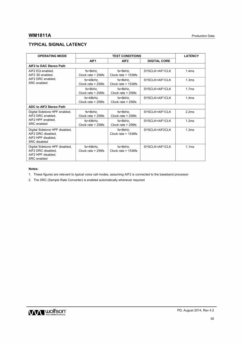
WM1811A Production Data
w PD, August 2014, Rev 4.2
30
TYPICAL SIGNAL LATENCY
OPERATING MODE TEST CONDITIONS LATENCY
AIF1 AIF2 DIGITAL CORE
AIF2 to DAC Stereo Path
AIF2 EQ enabled, AIF2 3D enabled, AIF2 DRC enabled, SRC enabled
fs=8kHz, Clock rate = 256fs
fs=8kHz, Clock rate = 1536fs
SYSCLK=AIF1CLK 1.4ms
fs=48kHz, Clock rate = 256fs
fs=8kHz, Clock rate = 1536fs
SYSCLK=AIF1CLK 1.3ms
fs=8kHz, Clock rate = 256fs
fs=8kHz, Clock rate = 256fs
SYSCLK=AIF1CLK 1.7ms
fs=48kHz, Clock rate = 256fs
fs=8kHz, Clock rate = 256fs
SYSCLK=AIF1CLK 1.4ms
ADC to AIF2 Stereo Path
Digital Sidetone HPF enabled, AIF2 DRC enabled, AIF2 HPF enabled, SRC enabled
fs=8kHz, Clock rate = 256fs
fs=8kHz, Clock rate = 256fs
SYSCLK=AIF1CLK 2.2ms
fs=48kHz, Clock rate = 256fs
fs=8kHz, Clock rate = 256fs
SYSCLK=AIF1CLK 1.2ms
Digital Sidetone HPF disabled, AIF2 DRC disabled, AIF2 HPF disabled, SRC disabled
fs=8kHz, Clock rate = 1536fs
SYSCLK=AIF2CLK 1.3ms
Digital Sidetone HPF disabled, AIF2 DRC disabled, AIF2 HPF disabled, SRC enabled
fs=48kHz, Clock rate = 256fs
fs=8kHz, Clock rate = 1536fs
SYSCLK=AIF1CLK 1.1ms
Notes:
1. These figures are relevant to typical voice call modes, assuming AIF2 is connected to the baseband processor
2. The SRC (Sample Rate Converter) is enabled automatically whenever required

Production Data WM1811A
w PD, August 2014, Rev 4.2
31
SIGNAL TIMING REQUIREMENTS
SYSTEM CLOCKS & FREQUENCY LOCKED LOOP (FLL)
Figure 1 Master Clock Timing
Test Conditions
The following timing information is valid across the full range of recommended operating conditions.
PARAMETER SYMBOL CONDITIONS MIN TYP MAX UNIT
Master Clock Timing (MCLK1 and MCLK2)
MCLK cycle time TMCLKY
MCLK as input to FLL, FLLn_REFCLK_DIV = 10, 11
25 ns
MCLK as input to FLL, FLLn_REFCLK_DIV = 01
37
MCLK as input to FLL, FLLn_REFCLK_DIV = 00
74
FLL not used, AIFnCLK_DIV = 1 40
FLL not used, AIFnCLK_DIV = 0 80
MCLK duty cycle
(= TMCLKH : TMCLKL)
60:40 40:60
Frequency Locked Loops (FLL1 and FLL2)
FLL Input Frequency FLLn_REFCLK_DIV = 00 0.032 13.5 MHz
FLLn_REFCLK_DIV = 01 0.064 27
FLLn_REFCLK_DIV = 10 0.128 40
FLLn_REFCLK_DIV = 11 0.256 40
Internal Clocking
AIF1CLK frequency 12.5 MHz
AIF2CLK frequency 12.5 MHz
SYSCLK frequency 12.5 MHz

WM1811A Production Data
w PD, August 2014, Rev 4.2
32
AUDIO INTERFACE TIMING
DIGITAL MICROPHONE (DMIC) INTERFACE TIMING
Figure 2 Digital Microphone Interface Timing
Test Conditions
The following timing information is valid across the full range of recommended operating conditions.
PARAMETER SYMBOL MIN TYP MAX UNIT
Digital Microphone Interface Timing
DMICCLK cycle time tCY 320 ns
DMICCLK duty cycle 45:55 55:45
DMICDAT (Left) setup time to falling DMICCLK edge tLSU 15 ns
DMICDAT (Left) hold time from falling DMICCLK edge tLH 0 ns
DMICDAT (Right) setup time to rising DMICCLK edge tRSU 15 ns
DMICDAT (Right) hold time from rising DMICCLK edge tRH 0 ns

Production Data WM1811A
w PD, August 2014, Rev 4.2
33
DIGITAL AUDIO INTERFACE - MASTER MODE
Figure 3 Audio Interface Timing - Master Mode
Note that BCLK and LRCLK outputs can be inverted if required; Figure 3 shows the default, non-inverted polarity of these signals.
Test Conditions
The following timing information is valid across the full range of recommended operating conditions.
PARAMETER SYMBOL MIN TYP MAX UNIT
Audio Interface Timing - Master Mode
BCLK cycle time tBCY 160 ns
LRCLK propagation delay from BCLK falling edge tDL 20 ns
ADCDAT propagation delay from BCLK falling edge tDDA 48 ns
DACDAT setup time to BCLK rising edge tDST 32 ns
DACDAT hold time from BCLK rising edge tDHT 10 ns
Audio Interface Timing - Ultrasonic (4FS) Master Mode
BCLK cycle time tBCY 80 ns
ADCDAT propagation delay from BCLK falling edge tDDA 24 ns
Note that the descriptions above assume non-inverted polarity of BCLK and LRCLK.

WM1811A Production Data
w PD, August 2014, Rev 4.2
34
DIGITAL AUDIO INTERFACE - SLAVE MODE
Figure 4 Audio Interface Timing - Slave Mode
Note that BCLK and LRCLK inputs can be inverted if required; Figure 4 shows the default, non-inverted polarity.
Test Conditions
The following timing information is valid across the full range of recommended operating conditions.
PARAMETER SYMBOL MIN TYP MAX UNIT
Audio Interface Timing - Slave Mode
BCLK cycle time tBCY 160 ns
BCLK pulse width high tBCH 64 ns
BCLK pulse width low tBCL 64 ns
LRCLK set-up time to BCLK rising edge tLRSU 10 ns
LRCLK hold time from BCLK rising edge tLRH 10 ns
DACDAT hold time from BCLK rising edge tDH 10 ns
ADCDAT propagation delay from BCLK falling edge tDD 48 ns
DACDAT set-up time to BCLK rising edge tDS 32 ns
Note that the descriptions above assume non-inverted polarity of BCLK and LRCLK.

Production Data WM1811A
w PD, August 2014, Rev 4.2
35
DIGITAL AUDIO INTERFACE - TDM MODE
When TDM operation is used on the ADCDATn pins, it is important that two devices do not attempt to drive the ADCDATn pin simultaneously. To support this requirement, the ADCDATn pins can be configured to be tri-stated when not outputting data.
The timing of the ADCDATn tri-stating at the start and end of the data transmission is described in Figure 5 below.
BCLK
ADCDAT
ADCDAT set-up time ADCDAT release time
ADCDAT undriven (tri-state) ADCDAT valid (CODEC output) ADCDAT valid ADCDAT undriven (tri-state)
Figure 5 Audio Interface Timing- TDM Mode
Test Conditions
The following timing information is valid across the full range of recommended operating conditions.
PARAMETER MIN TYP MAX UNIT
TDM Timing - Master Mode
ADCDATsetup time from BCLKfalling edge 0 ns
ADCDATrelease time from BCLKfalling edge 15 ns
TDM Timing - Slave Mode
ADCDAT setup time from BCLK falling edge 5 ns
ADCDAT release time from BCLK falling edge 32 ns
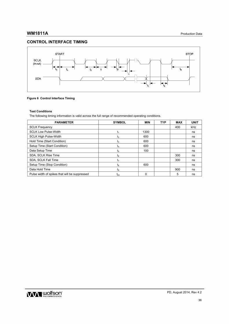
WM1811A Production Data
w PD, August 2014, Rev 4.2
36
CONTROL INTERFACE TIMING
Figure 6 Control Interface Timing
Test Conditions
The following timing information is valid across the full range of recommended operating conditions.
PARAMETER SYMBOL MIN TYP MAX UNIT
SCLK Frequency 400 kHz
SCLK Low Pulse-Width t1 1300 ns
SCLK High Pulse-Width t2 600 ns
Hold Time (Start Condition) t3 600 ns
Setup Time (Start Condition) t4 600 ns
Data Setup Time t5 100 ns
SDA, SCLK Rise Time t6 300 ns
SDA, SCLK Fall Time t7 300 ns
Setup Time (Stop Condition) t8 600 ns
Data Hold Time t9 900 ns
Pulse width of spikes that will be suppressed tps 0 5 ns

Production Data WM1811A
w PD, August 2014, Rev 4.2
37
DEVICE DESCRIPTION
INTRODUCTION
The WM1811A is a low power, high quality audio codec designed to interface with a wide range of processors and analogue components. A high level of mixed-signal integration in a very small footprint makes it ideal for portable applications such as mobile phones.Fully differential internal architecture and on-chip RF noise filters ensure a very high degree of noise immunity.
Three sets of audio interface pins are available in order to provide independent and fully asynchronous connections to multiple processors, typically an application processor, baseband processor and wireless transceiver. Any two of these interfaces can operate totally independently and asynchronously while the third interface can be synchronised to either of the other two and can also provide ultra low power loopback modes to support, for example, wireless headset voice calls.
The WM1811A provides a two-channel digital microphone interface, suitable for noise cancellation and other applications. An integrated microphone activity monitor is available to enable the processor to sleep during periods of microphone inactivity, saving power.
Eight highly flexible analogue inputs allow interfacing to up to four microphone inputs (single-ended or differential), plus multiple stereo or mono line inputs. Connections to an external voice CODEC, FM radio, line input, handset MIC and headset MIC are all fully supported. Signal routing to the output mixers and within the CODEC has been designed for maximum flexibility to support a wide variety of usage modes.
Impedance sensing and measurement for external accessories is provided, for detection of the insertion or removal of microphones and other accessories. Push-button detection of up to 7 inputs can be supported using this feature.Low power jack detection is supported, using a dedicated input pin; this enables power consumption to be minimised in standby conditions, whilst awaiting an external jack insertion event.
Nine analogue output drivers are integrated, including a stereo pair of high power, high quality Class D speaker drivers; these can support 2Weach in stereo mode. It is also possible to configure the speaker drivers as a mono output, giving enhanced performance. A mono earpiece driver is provided, providing an additional output from the output mixers.
One pair of ground-referenced headphone outputs is provided; these are powered from an integrated Charge Pump, enabling high quality, power efficient headphone playback without any requirement for DC blocking capacitors. A DC Servo circuit is available for DC offset correction, thereby suppressing pops and reducing power consumption. Four line outputs are provided, with multiple configuration options including 4 x single-ended outputs or 2 x differential outputs. The line outputs are suitable for output to a voice CODEC, an external speaker driver or line output connector. Ground loop feedback is available on the headphone outputs and the line outputs, providing rejection of noise on the ground connections. All outputs have integrated pop and click suppression features.
Internal differential signal routing and amplifier configurations have been optimised to provide the highest performance and lowest possible power consumption for a wide range of usage scenarios, including voice calls and music playback. The speaker drivers offer low leakage and high PSRR; this enables direct connection to a Lithium battery. The speaker drivers provide eight levels of AC and DC gain to allow output signal levels to be maximised for many commonly-used SPKVDD/AVDD1 combinations.
The ADCs and DACs are of hi-fi quality, using a 24-bit low-order oversampling architecture to deliver optimum performance. A flexible clocking arrangement supports mixed sample rates, whilst integrated ultra-low power dual FLLs provide additional flexibility. A high pass filter is available in all ADC and digital MIC paths for removing DC offsets and suppressing low frequency noise such as mechanical vibration and wind noise. A digital mixing path from the ADC or digital MICs to the DAC provides a sidetone of enhanced quality during voice calls. DAC soft mute and un-mute is available for pop-free music playback.
The integrated Dynamic Range Controllers (DRC) and ReTuneTM Mobile 5-band parametric equaliser (EQ) provide further processing capability of the digital audio paths. The DRC provides compression and signal level control to improve the handling of unpredictable signal levels. ‘Anti-clip’ and ‘quick release’ algorithms improve intelligibility in the presence of transients and impulsive noises. The EQ provides the capability to tailor the audio path according to the frequency characteristics of an earpiece or loudspeaker, and/or according to user preferences.

WM1811A Production Data
w PD, August 2014, Rev 4.2
38
The WM1811A has highly flexible digital audio interfaces, supporting a number of protocols, including I2S, DSP, MSB-first left/right justified, and can operate in master or slave modes. PCM operation is supported in the DSP mode. A-law and -law companding are also supported. Time division multiplexing (TDM) is available to allow multiple devices to stream data simultaneously on the same bus, saving space and power.
A powerful digital mixing core allows data from each audio interface channel and from the ADCs and digital MICs to be mixed and re-routed back to a different audio interface and to the DAC output paths. The digital mixing core can operate synchronously with either Audio Interface 1 or Audio Interface 2, with asynchronous stereo full duplex sample rate conversion performed on the other audio interface as required.
The system clock (SYSCLK) provides clocking for the ADCs, DACs, DSP core, digital audio interface and other circuits. SYSCLK can be derived directly from one of the MCLK1 or MCLK2 pins or via one of two integrated FLLs, providing flexibility to support a wide range of clocking schemes, including self-clocking FLL modes. Typical portable system MCLK frequencies, and sample rates from 8kHz to 96kHz are all supported. A low frequency (eg. 32.768kHz) clock can be used as the input reference to the FLLs, providing further flexibility. Automatic configuration of the clocking circuits is available, derived from the sample rate and from the MCLK / SYSCLK ratio.
The WM1811A uses a standard 2-wire control interface, providing full software control of all features, together with device register readback. It is an ideal partner for a wide range of industry standard microprocessors, controllers and DSPs. Unused circuitry can be disabled under software control, in order to save power; low leakage currents enable extended standby/off time in portable battery-powered applications.
Versatile GPIO functionality is provided, with support for button/accessory detect inputs, or for clock, system status, or programmable logic level output for control of additional external circuitry. Interrupt logic, status readback and de-bouncing options are supported within this functionality.
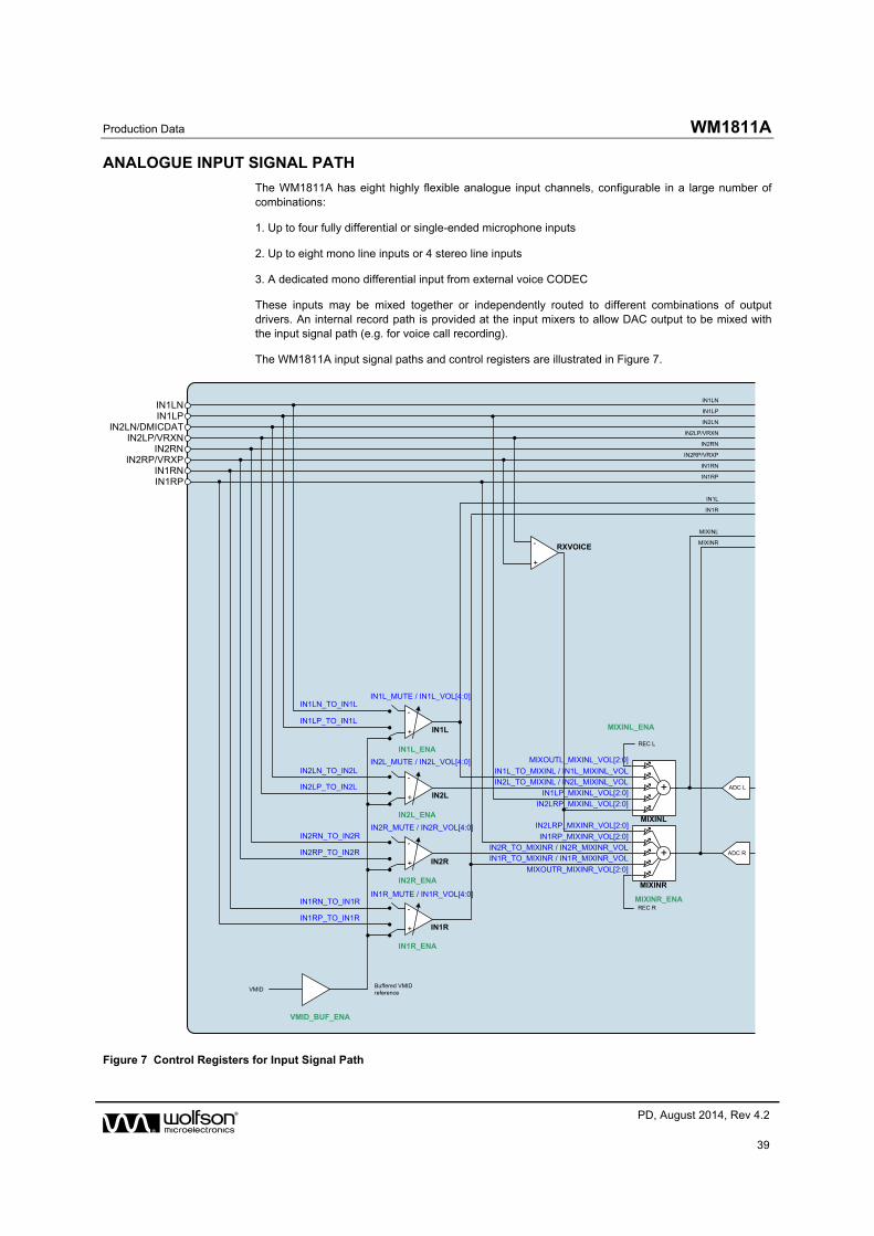
Production Data WM1811A
w PD, August 2014, Rev 4.2
39
ANALOGUE INPUT SIGNAL PATH
The WM1811A has eight highly flexible analogue input channels, configurable in a large number of combinations:
1. Up to four fully differential or single-ended microphone inputs
2. Up to eight mono line inputs or 4 stereo line inputs
3. A dedicated mono differential input from external voice CODEC
These inputs may be mixed together or independently routed to different combinations of output drivers. An internal record path is provided at the input mixers to allow DAC output to be mixed with the input signal path (e.g. for voice call recording).
The WM1811A input signal paths and control registers are illustrated in Figure 7.
IN1LPIN1LN
IN1RN
IN2LN/DMICDAT
IN2RN
IN1RP
IN2LP/VRXN
IN2RP/VRXP
MIXINR
IN1L
IN2L
IN2R
IN1R
RXVOICE
MIXINL
+
-
+
-
+
-
+
-
+
-
REC L
REC R
+
+
IN2L_ENA
MIXINL_ENA
IN1L_MUTE / IN1L_VOL[4:0]
IN1LP_TO_IN1L
IN2LRP_MIXINL_VOL[2:0]
IN2R_TO_MIXINR / IN2R_MIXINR_VOL
IN2L_TO_MIXINL / IN2L_MIXINL_VOL
IN1L_TO_MIXINL / IN1L_MIXINL_VOL
MIXOUTL_MIXINL_VOL[2:0]
IN1LP_MIXINL_VOL[2:0]
MIXINR_ENA
IN2LRP_MIXINR_VOL[2:0]
IN1RP_MIXINR_VOL[2:0]
MIXOUTR_MIXINR_VOL[2:0]
IN1R_TO_MIXINR / IN1R_MIXINR_VOL
IN1L_ENA
IN2R_ENA
IN1R_ENA
IN2L_MUTE / IN2L_VOL[4:0]
IN1R_MUTE / IN1R_VOL[4:0]
IN2R_MUTE / IN2R_VOL[4:0]
IN1RN_TO_IN1R
IN1RP_TO_IN1R
IN2RN_TO_IN2R
IN2RP_TO_IN2R
IN2LN_TO_IN2L
IN2LP_TO_IN2L
IN1LN_TO_IN1L
IN1R
IN1L
MIXINR
MIXINL
IN1LP
IN1LN
IN1RN
IN2LN
IN2RN
IN1RP
IN2LP/VRXN
IN2RP/VRXP
ADC R
ADC L
VMID_BUF_ENA
VMIDBuffered VMID reference
Figure 7 Control Registers for Input Signal Path

WM1811A Production Data
w PD, August 2014, Rev 4.2
40
MICROPHONE INPUTS
Up to four analogue microphones can be connected to the WM1811A, either in single-ended or differential mode. A dedicated PGA is provided for each microphone input. Two low noise microphone bias circuits are provided, reducing the need for external components.
For single-ended microphone inputs, the microphone signal is connected to the inverting input of the PGAs (IN1LN, IN2LN, IN1RN or IN2RN). The non-inverting inputs of the PGAs are internally connected to VMID in this configuration. The non-inverting input pins IN1LP, IN2LP, IN1RP and IN2RP are free to be used as line connections to the input or output mixers in this configuration.
For differential microphone inputs, the non-inverted microphone signal is connected to the non-inverting input of the PGAs (IN1LP, IN2LP, IN1RP or IN2RP), whilst the inverted (or ‘noisy ground’) signal is connected to the inverting input pins (IN1LN, IN2LN, IN1RN and IN2RN).
The gain of the input PGAs is controlled via register settings, as defined in Table 4. Note that the input impedance of both inverting and non-inverting inputs changes with the input PGA gain setting, as described under “Electrical Characteristics”.See also the “Applications Information” for details of input resistance at all PGA Gain settings.
The microphone input configurations are illustrated in Figure 8 and Figure 9. Note that any PGA input pin that is used in either microphone configuration is not available for use as a line input path at the same time.
MIC
GND
To input mixers
-
+
PGAVMID
MICBIAS
IN1LN, IN2LN, IN1RN, IN2RN
IN1LP, IN2LP, IN1RP, IN2RP
Figure 8 Single-Ended Microphone Input Figure 9 Differential Microphone Input
MICROPHONE BIAS CONTROL
There are two MICBIAS generators which provide low noise reference voltages suitable for powering silicon (MEMS) microphones or biasing electret condenser (ECM) type microphones via an external resistor. Refer to the “Applications Information” section for recommended external components.
The MICBIAS outputs can be independently enabled using the MICB1_ENA and MICB2_ENA register bits. Under default conditions, a smooth pop-free profile of the MICBIAS outputs is implemented when MICB1_ENA or MICB2_ENA is enabled or disabled; a faster transition can be selected by setting the MICB1_RATE and MICB2_RATE registers as described in Table 1.
When a MICBIAS output is disabled, the output pin can be configured to be floating or to be actively discharged. This is selected using the MICB1_DISCH and MICB2_DISCH register bits.
The MICBIAS generators can each operate as a voltage regulator or in bypass mode.
In Regulator mode, the output voltage is selected using the MICB1_LVL and MICB2_LVL register bits.In this mode, AVDD1 must be at least 200mV greater than the required MICBIAS output voltages.The MICBIAS outputs are powered from the AVDD1 supply pin, and use the internal bandgap circuit as a reference.
Note that, in Regulator mode, the MICBIAS regulators are designed to operate without external decoupling capacitors. It is important that parasitic capacitances on the MICBIAS1 or MICBIAS2 pins do not exceed the specified limit in Regulator mode (see “Electrical Characteristics”).
In Bypass mode, the output pin (MICBIAS1 or MICBIAS2) is connected directly to AVDD1. This enables a low power operating state. Note that, if a capacitive load is connected to MICBIAS1 or

Production Data WM1811A
w PD, August 2014, Rev 4.2
41
MICBIAS2 (eg. for a digital microphone supply), then the respective MICBIAS generator must be configured in Bypass mode.
The MICBIAS configuration is illustrated in Figure 10.
Figure 10 MICBIAS Generator
REGISTER ADDRESS
BIT LABEL DEFAULT DESCRIPTION
R1 (0001h)
Power Management (1)
5 MICB2_ENA 0 Microphone Bias 2 Enable
0 = Disabled
1 = Enabled
4 MICB1_ENA 0 Microphone Bias 1 Enable
0 = Disabled
1 = Enabled
R61 (003Dh)
MICBIAS 1
5 MICB1_RATE 1 Microphone Bias 1 Rate
0 = Fast start-up / shut-down
1 = Pop-free start-up / shut-down
4 MICB1_MODE 1 Microphone Bias 1 Mode
0 = Regulator mode
1 = Bypass mode
3:1 MICB1_LVL [2:0] 100 Microphone Bias 1 Voltage Control
(when MICB1_MODE = 0)
000 = 1.5V
001 = 1.8V
010 = 1.9V
011 = 2.0V
100 = 2.2V
101 = 2.4V
110 = 2.5V
111 = 2.6V
0 MICB1_DISCH 1 Microphone Bias 1 Discharge
0 = MICBIAS1 floating when disabled
1 = MICBIAS1 discharged when disabled
R62 (003Eh)
MICBIAS
5 MICB2_RATE 1 Microphone Bias 2 Rate
0 = Fast start-up / shut-down
1 = Pop-free start-up / shut-down
WM1811A Production Data
w PD, August 2014, Rev 4.2
42
REGISTER ADDRESS
BIT LABEL DEFAULT DESCRIPTION
2 4 MICB2_MODE 1 Microphone Bias 2 Mode
0 = Regulator mode
1 = Bypass mode
3:1 MICB2_LVL [2:0] 100 Microphone Bias 2 Voltage Control
(when MICB2_MODE = 0)
000 = 1.5V
001 = 1.8V
010 = 1.9V
011 = 2.0V
100 = 2.2V
101 = 2.4V
110 = 2.5V
111 = 2.6V
0 MICB2_DISCH 1 Microphone Bias 2 Discharge
0 = MICBIAS2 floating when disabled
1 = MICBIAS2 discharged when disabled
Table 1 Microphone Bias Control
Note that the maximum source current capability for MICBIAS1 and MICBIAS2 is 2.4mA each in Regulator mode. The external biasing resistance must be large enough to limit each MICBIAS current to 2.4mA across the full microphone impedance range. The maximum source current for MICBIAS1 and MICBIAS2 is 3.6mA each in Bypass mode, as described in the “Electrical Characteristics”.
MICROPHONE ACCESSORY DETECT
The WM1811A provides a microphone detection function, which uses impedance measurement to detect one or more different external accessory connections. This feature is described in the “External Accessory Detection” section.
LINE AND VOICE CODEC INPUTS
All eight analogue input pins may be used as line inputs. Each line input has different signal path options, providing flexibility, high performance and low power consumption for many different usage modes.
IN1LN and IN1RN can operate as single-ended line inputs to the input PGAs IN1L and IN1R respectively. These inputs provide a high gain path if required for low input signal levels.
IN2LN and IN2RN can operate as single-ended line inputs to the input PGAs IN2L and IN2R respectively, providing further high gain signal paths. These pins can also be connected to either of the output mixers MIXOUTL and MIXOUTR.
IN1LP and IN1RP can operate as single-ended line inputs to the input mixers MIXINL and MIXINR, or to the speaker mixers SPKMIXL and SPKMIXR. These signal paths enable power consumption to be reduced, by allowing the input PGAs and other circuits to be disabled if not required.
IN2LP/VRXN and IN2RP/VRXP can operate in three different ways:
Mono differential ’RXVOICE’ input (e.g. from an external voice CODEC) to the input mixers MIXINL and MIXINR.
Single-ended line inputs to either of the output mixers MIXOUTL and MIXOUTR.
Signal path configuration to the input PGAs and input mixers is detailed later in this section. Signal path configuration to the output mixers and speaker mixers is described in “Analogue Output Signal Path”.

Production Data WM1811A
w PD, August 2014, Rev 4.2
43
The line input and voice CODEC input configurations are illustrated in Figure 11 through to Figure 14.
Figure 11 IN1LN or IN1RN as Line Inputs Figure 12 IN2LN or IN2RN as Line Inputs
Figure 13 IN1LP or IN1RP as Line Inputs Figure 14 IN2LP or IN2RP as Line Inputs
INPUT PGA ENABLE
The Input PGAs are enabled using register bits IN1L_ENA, IN2L_ENA, IN1R_ENA and IN2R_ENA, as described in Table 2. The Input PGAs must be enabled for microphone input on the respective input pins, or for line input on the inverting input pins IN1LN, IN1RN, IN2LN, IN2RN.
REGISTER ADDRESS
BIT LABEL DEFAULT DESCRIPTION
R2 (0002h)
Power Management (2)
7 IN2L_ENA 0 IN2L Input PGA Enable
0 = Disabled
1 = Enabled
6 IN1L_ENA 0 IN1L Input PGA Enable
0 = Disabled
1 = Enabled
5 IN2R_ENA 0 IN2R Input PGA Enable
0 = Disabled
1 = Enabled
4 IN1R_ENA 0 IN1R Input PGA Enable
0 = Disabled
1 = Enabled
Table 2 Input PGA Enable
For normal operation of the input PGAs, the reference voltage VMID and the bias current must also be enabled. See “Reference Voltages and Master Bias” for details of the associated controls VMID_SEL and BIAS_ENA.

WM1811A Production Data
w PD, August 2014, Rev 4.2
44
INPUT PGA CONFIGURATION
Each of the Input PGAs can operate in a single-ended ordifferential mode. In differential mode, both inputs to the PGA are connected to the input source. In single-ended mode, the non-inverting input to the PGA must be connected to VMID. Configuration of the PGA inputs to the WM1811A input pins is controlled using the register bits shown in Table 3.
Single-ended microphone operation is configured by connecting the input source to the inverting input of the applicable PGA. The non-inverting input of the PGA must be connected to the buffered VMID reference. Note that the buffered VMID reference must be enabled, using the VMID_BUF_ENA register, as described in “Reference Voltages and Master Bias”.
Differential microphone operation is configured by connecting the input source to both inputs of the applicable PGA.
Line inputs to the input pins IN1LN, IN2LN, IN1RN and IN2RN must be connected to the applicable PGA. The non-inverting input of the PGA must be connected to VMID.
Line inputs to the input pins IN1LP, IN2LP, IN1RP or IN2RP do not connect to the input PGAs. The non-inverting inputs of the associated PGAs must be connected to VMID. The inverting inputs of the associated PGAs may be used as separate mic/line inputs if required.
The maximum available attenuation on any of these input paths is achieved by using register bits shown in Table 3 to disconnect the input pins from the applicable PGA.
Production Data WM1811A
w PD, August 2014, Rev 4.2
45
REGISTER ADDRESS
BIT LABEL DEFAULT DESCRIPTION
R40 (0028h)
Input Mixer (2)
7 IN2LP_TO_IN2L 0 IN2L PGA Non-Inverting Input Select 0 = Connected to VMID 1 = Connected to IN2LP
Note that VMID_BUF_ENA must be set when using IN2L connected to VMID.
6 IN2LN_TO_IN2L 0 IN2L PGA Inverting Input Select 0 = Not connected 1 = Connected to IN2LN
5 IN1LP_TO_IN1L 0 IN1L PGA Non-Inverting Input Select 0 = Connected to VMID 1 = Connected to IN1LP
Note that VMID_BUF_ENA must be set when using IN1L connected to VMID.
4 IN1LN_TO_IN1L 0 IN1L PGA Inverting Input Select 0 = Not connected 1 = Connected to IN1LN
3 IN2RP_TO_IN2R 0 IN2R PGA Non-Inverting Input Select 0 = Connected to VMID 1 = Connected to IN2RP
Note that VMID_BUF_ENA must be set when using IN2R connected to VMID.
2 IN2RN_TO_IN2R 0 IN2R PGA Inverting Input Select 0 = Not connected 1 = Connected to IN2RN
1 IN1RP_TO_IN1R 0 IN1R PGA Non-Inverting Input Select 0 = Connected to VMID 1 = Connected to IN1RP
Note that VMID_BUF_ENA must be set when using IN1R connected to VMID.
0 IN1RN_TO_IN1R 0 IN1R PGA Inverting Input Select 0 = Not connected 1 = Connected to IN1RN
Table 3 Input PGA Configuration
INPUT PGA VOLUME CONTROL
Each of the four Input PGAs has an independently controlled gain range of -16.5dB to +30dB in 1.5dB steps. The gains on the inverting and non-inverting inputs to the PGAs are always equal. Each Input PGA can be independently muted using the PGA mute bits as described in Table 4, with maximum mute attenuation achieved by simultaneously disconnecting the corresponding inputs described in Table 3.
Note that, under default conditions (following power-up or software reset), the PGA mute register bits are set to ‘1’, but the mute functions will only become effective after the respective bit has been toggled to ‘0’ and then back to ‘1’. The Input PGAs will be un-muted (Mute disabled) after power-up or software reset, regardless of the readback value of the respective PGA mute bits.
To prevent "zipper noise", a zero-cross function is provided on the input PGAs. When this feature is enabled, volume updates will not take place until a zero-crossing is detected. In the case of a long period without zero-crossings, a timeout function is provided. When the zero-cross function is enabled, the volume will update after the timeout period if no earlier zero-cross has occurred. The timeout clock is enabled using TOCLK_ENA, the timeout period is set by TOCLK_DIV. See “Clocking and Sample Rates” for more information on these fields.

WM1811A Production Data
w PD, August 2014, Rev 4.2
46
The IN1_VU and IN2_VU bits control the loading of the input PGA volume data. When IN1_VU and IN2_VU are set to 0, the PGA volume data will be loaded into the respective control register, but will not actually change the gain setting. The IN1L and IN1R volume settings are both updated when a 1 is written to IN1_VU; the IN2L and IN2R volume settings are both updated when a 1 is written to IN2_VU. This makes it possible to update the gain of the left and right signal paths simultaneously.
The Input PGA Volume Control register fields are described in Table 4 and Table 5.
REGISTER ADDRESS
BIT LABEL DEFAULT DESCRIPTION
R24 (0018h)
Left Line Input 1&2 Volume
8 IN1_VU N/A Input PGA Volume Update
Writing a 1 to this bit will cause IN1L and IN1R input PGA volumes to be updated simultaneously
7 IN1L_MUTE 1 IN1L PGA Mute
0 = Disable Mute
1 = Enable Mute
6 IN1L_ZC 0 IN1L PGA Zero Cross Detector
0 = Change gain immediately
1 = Change gain on zero cross only
4:0 IN1L_VOL [4:0]
01011
(0dB)
IN1L Volume
-16.5dB to +30dB in 1.5dB steps
(See Table 5 for volume range)

Production Data WM1811A
w PD, August 2014, Rev 4.2
47
REGISTER ADDRESS
BIT LABEL DEFAULT DESCRIPTION
R25 (0019h)
Left Line Input 3&4 Volume
8 IN2_VU N/A Input PGA Volume Update
Writing a 1 to this bit will cause IN2L and IN2R input PGA volumes to be updated simultaneously
7 IN2L_MUTE 1 IN2L PGA Mute
0 = Disable Mute
1 = Enable Mute
6 IN2L_ZC 0 IN2L PGA Zero Cross Detector
0 = Change gain immediately
1 = Change gain on zero cross only
4:0 IN2L_VOL[4:0]
01011
(0dB)
IN2L Volume
-16.5dB to +30dB in 1.5dB steps
(See Table 5 for volume range)
R26 (001Ah)
Right Line Input 1&2 Volume
8 IN1_VU N/A Input PGA Volume Update
Writing a 1 to this bit will cause IN1L and IN1R input PGA volumes to be updated simultaneously
7 IN1R_MUTE 1 IN1R PGA Mute
0 = Disable Mute
1 = Enable Mute
6 IN1R_ZC 0 IN1R PGA Zero Cross Detector
0 = Change gain immediately
1 = Change gain on zero cross only
4:0 IN1R_VOL[4:0]
01011
(0dB)
IN1R Volume
-16.5dB to +30dB in 1.5dB steps
(See Table 5 for volume range)
R27 (001Bh)
Right Line Input 3&4 Volume
8 IN2_VU N/A Input PGA Volume Update
Writing a 1 to this bit will cause IN2L and IN2R input PGA volumes to be updated simultaneously
7 IN2R_MUTE 1 IN2R PGA Mute
0 = Disable Mute
1 = Enable Mute
6 IN2R_ZC 0 IN2R PGA Zero Cross Detector
0 = Change gain immediately
1 = Change gain on zero cross only
4:0 IN2R_VOL[4:0]
01011
(0dB)
IN2R Volume
-16.5dB to +30dB in 1.5dB steps
(See Table 5 for volume range)
Table 4 Input PGA Volume Control

WM1811A Production Data
w PD, August 2014, Rev 4.2
48
IN1L_VOL[4:0], IN2L_VOL[4:0], IN1R_VOL[4:0], IN2R_VOL[4:0]
VOLUME
(dB)
00000 -16.5
00001 -15.0
00010 -13.5
00011 -12.0
00100 -10.5
00101 -9.0
00110 -7.5
00111 -6.0
01000 -4.5
01001 -3.0
01010 -1.5
01011 0
01100 +1.5
01101 +3.0
01110 +4.5
01111 +6.0
10000 +7.5
10001 +9.0
10010 +10.5
10011 +12.0
10100 +13.5
10101 +15.0
10110 +16.5
10111 +18.0
11000 +19.5
11001 +21.0
11010 +22.5
11011 +24.0
11100 +25.5
11101 +27.0
11110 +28.5
11111 +30.0
Table 5 Input PGA Volume Range

Production Data WM1811A
w PD, August 2014, Rev 4.2
49
INPUT MIXER ENABLE
The WM1811A has two analogue input mixers which allow the Input PGAs and Line Inputs to be combined in a number of ways and output to the ADCs, Output Mixers, or directly to the output drivers via bypass paths.
The input mixers MIXINL and MIXINR are enabled by the MIXINL_ENA and MIXINR_ENA register bits, as described in Table 6. These control bits also enable the RXVOICE input path, described in the following section.
For normal operation of the input mixers, the reference voltage VMID and the bias current must also be enabled. See “Reference Voltages and Master Bias” for details of the associated controls VMID_SEL and BIAS_ENA.
REGISTER ADDRESS
BIT LABEL DEFAULT DESCRIPTION
R2 (0002h)
Power Management (2)
9 MIXINL_ENA 0 Left Input Mixer Enable
(Enables MIXINL and RXVOICE input to MIXINL)
0 = Disabled
1 = Enabled
8 MIXINR_ENA 0 Right Input Mixer Enable
(Enables MIXINR and RXVOICE input to MIXINR)
0 = Disabled
1 = Enabled
Table 6 Input Mixer Enable
INPUT MIXER CONFIGURATION AND VOLUME CONTROL
The left and right channel input mixers MIXINL and MIXINR can be configured to take input from up to five sources:
1. IN1L or IN1R Input PGA
2. IN2L or IN2R Input PGA
3. IN1LP or IN1RP pin (PGA bypass)
4. RXVOICE mono differential input from IN2LP/VRXN and IN2RP/VRXP
5. MIXOUTL or MIXOUTR Output Mixer (Record path)
The Input Mixer configuration and volume controls are described in Table 7 for the Left input mixer (MIXINL) and Table 8 for the Right input mixer (MIXINR). The signal levels from the Input PGAs may be set to Mute, 0dB or 30dB boost. Gain controls for the PGA bypass, RXVOICE and Record paths provide adjustment from -12dB to +6dB in 3dB steps.
When using the IN1LP or IN1RP signal paths direct to the input mixers (PGA bypass paths), a signal gain of +15dB can be selected using the IN1RP_MIXINR_BOOST or IN1LP_MIXINL_BOOST register bits. See Table 7 and Table 8 for further details.
When using the IN1LP or IN1RP signal paths direct to the input mixers (PGA bypass paths), the buffered VMID reference must be enabled, using the VMID_BUF_ENA register, as described in “Reference Voltages and Master Bias”.
To prevent pop noise, it is recommended that gain and mute controls for the input mixers are not modified while the signal paths are active. If volume control is required on these signal paths, it is recommended that this is implemented using the input PGA volume controls or the ADC volume controls. The ADC volume controls are described in the “Analogue to Digital Converter (ADC)” section.

WM1811A Production Data
w PD, August 2014, Rev 4.2
50
REGISTER ADDRESS
BIT LABEL DEFAULT DESCRIPTION
R21 (0015h)
Input Mixer (1)
7 IN1LP_MIXINL_BOOST 0 IN1LP Pin (PGA Bypass) to MIXINL Gain Boost.
This bit selects the maximum gain setting of the IN1LP_MIXINL_VOL register.
0 = Maximum gain is +6dB
1 = Maximum gain is +15dB
R41 (0029h)
Input Mixer (3)
8 IN2L_TO_MIXINL 0 IN2L PGA Output to MIXINL Mute
0 = Mute
1 = Un-Mute
7 IN2L_MIXINL_VOL 0 IN2L PGA Output to MIXINL Gain
0 = 0dB
1 = +30dB
5 IN1L_TO_MIXINL 0 IN1L PGA Output to MIXINL Mute
0 = Mute
1 = Un-Mute
4 IN1L_MIXINL_VOL 0 IN1L PGA Output to MIXINL Gain
0 = 0dB
1 = +30dB
2:0 MIXOUTL_MIXINL_VOL
[2:0]
000
(Mute)
Record Path MIXOUTL to MIXINL Gain and Mute
000 = Mute
001 = -12dB
010 = -9dB
011 = -6dB
100 = -3dB
101 = 0dB
110 = +3dB
111 = +6dB
R43 (002Bh)
Input Mixer (5)
8:6 IN1LP_MIXINL_VOL
[2:0]
000
(Mute)
IN1LP Pin (PGA Bypass) to MIXINL Gain and Mute
000 = Mute
001 = -12dB
010 = -9dB
011 = -6dB
100 = -3dB
101 = 0dB
110 = +3dB
111 = +6dB (see note below).
When IN1LP_MIXINL_BOOST is set, then the maximum gain setting is increased to +15dB, ie. 111 = +15dB.
Note that VMID_BUF_ENA must be set when using the IN1LP (PGA Bypass) input to MIXINL.

Production Data WM1811A
w PD, August 2014, Rev 4.2
51
REGISTER ADDRESS
BIT LABEL DEFAULT DESCRIPTION
2:0 IN2LRP_MIXINL_VOL
[2:0]
000
(Mute)
RXVOICE Differential Input (VRXP-VRXN) to MIXINL Gain and Mute
000 = Mute
001 = -12dB
010 = -9dB
011 = -6dB
100 = -3dB
101 = 0dB
110 = +3dB
111 = +6dB
Table 7 Left Input Mixer (MIXINL) Volume Control
REGISTER ADDRESS
BIT LABEL DEFAULT DESCRIPTION
R21 (0015h)
Input Mixer (1)
8 IN1RP_MIXINR_BOOST 0 IN1RP Pin (PGA Bypass) to MIXINR Gain Boost.
This bit selects the maximum gain setting of the IN1RP_MIXINR_VOL register.
0 = Maximum gain is +6dB
1 = Maximum gain is +15dB
R42 (002A)
Input Mixer (4)
8 IN2R_TO_MIXINR 0 IN2R PGA Output to MIXINR Mute
0 = Mute
1 = Un-Mute
7 IN2R_MIXINR_VOL 0 IN2R PGA Output to MIXINR Gain
0 = 0dB
1 = +30dB
5 IN1R_TO_MIXINR 0 IN1R PGA Output to MIXINR Mute
0 = Mute
1 = Un-Mute
4 IN1R_MIXINR_VOL 0 IN1R PGA Output to MIXINR Gain
0 = 0dB
1 = +30dB
2:0 MIXOUTR_MIXINR_VOL
[2:0]
000
(Mute)
Record Path MIXOUTR to MIXINR Gain and Mute
000 = Mute
001 = -12dB
010 = -9dB
011 = -6dB
100 = -3dB
101 = 0dB
110 = +3dB
111 = +6dB

WM1811A Production Data
w PD, August 2014, Rev 4.2
52
REGISTER ADDRESS
BIT LABEL DEFAULT DESCRIPTION
R44 (002Ch)
Input Mixer (6)
8:6 IN1RP_MIXINR_VOL
[2:0]
000
(Mute)
IN1RP Pin (PGA Bypass) to MIXINR Gain and Mute
000 = Mute
001 = -12dB
010 = -9dB
011 = -6dB
100 = -3dB
101 = 0dB
110 = +3dB
111 = +6dB (see note below).
When IN1RP_MIXINR_BOOST is set, then the maximum gain setting is increased to +15dB, ie. 111 = +15dB.
Note that VMID_BUF_ENA must be set when using the IN1RP (PGA Bypass) input to MIXINR.
2:0 IN2LRP_MIXINR_VOL
[2:0]
000
(Mute)
RXVOICE Differential Input (VRXP-VRXN) to MIXINR Gain and Mute
000 = Mute
001 = -12dB
010 = -9dB
011 = -6dB
100 = -3dB
101 = 0dB
110 = +3dB
111 = +6dB
Table 8 Right Input Mixer (MIXINR) Volume Control

Production Data WM1811A
w PD, August 2014, Rev 4.2
53
DIGITAL MICROPHONE INTERFACE
The WM1811A supports a stereo digital microphone interface. Two channels of audio data are multiplexed on the DMICDAT pin; the data is clocked using the DMICCLK output pin.
The DMICDAT function is shared with the IN2LN pin; the analogue signal paths from IN2LN cannot be used when this pin is used for DMICDAT digital microphone input.
The digital microphone interface is referenced to the MICBIAS1 voltage domain; the MICBIAS1 output must be enabled (MICB1_ENA = 1) when using the digital microphone interface.
The MICBIAS1 generator is suitable for use as a low noise supply for the digital microphones. Note that, if the capacitive load on the MICBIAS1 generator exceeds the specified limit (eg. due to a decoupling capacitor or long PCB trace), then the MICBIAS1 generator must be configured in Bypass mode. See “Analogue Input Signal Path” for details of the MICBIAS1 generator.
When digital microphone input is enabled, the WM1811A outputs a clock signal on the DMICCLK pin.
A pair of digital microphones is connected as illustrated in Figure 15. The microphones must be configured to ensure that the Left mic transmits a data bit when DMICCLK is high, and the Right mic transmits a data bit when DMICCLK is low. The WM1811A samples the digital microphone data at the end of each DMICCLK phase. Each microphone must tri-state its data output when the other microphone is transmitting.
Figure 15 Digital Microphone Input
The DMICDAT digital microphone channels are enabled using DMIC1L_ENA and DMIC1R_ENA. When these signal paths are enabled, the respective ADC path is disconnected and the digital microphone data is routed to the digital mixing input bus, as illustrated in “Digital Mixing”.
Two microphone channels are interleaved on DMICDAT; the timing is illustrated in Figure 16. Each microphone must tri-state its data output when the other microphone is transmitting.

WM1811A Production Data
w PD, August 2014, Rev 4.2
54
DMICCLK pin
DMICDAT pin(Left & Right
channels interleaved)
1 2 1 2 1 2
Left Mic output 1 1 1
Right Mic output 2 2 2
hi-Z
Figure 16 Digital Microphone Interface Timing
The digital microphone channels can be routed to the AIF1 digital audio interface output paths.
Digital volume control of the digital microphone channels in the AIF1 signal paths is provided using the registers described in the “Digital Volume and Filter Control” section.
The digital microphone channels can also be routed, in a limited number of configurations, to the digital mixing output bus, via the digital sidetone signal paths. See “Digital Mixing” for further details.
Digital volume control of the digital microphone channels in the digital sidetone signal paths is provided using the registers described in the “Digital Mixing” section.
The digital microphone interface control fields are described in Table 9.
REGISTER ADDRESS
BIT LABEL DEFAULT DESCRIPTION
R4 (0004h)
Power Management (4)
3 DMIC1L_ENA 0 Digital microphone (DMICDAT) Left channel enable
0 = Disabled
1 = Enabled
2 DMIC1R_ENA 0 Digital microphone (DMICDAT) Right channel enable
0 = Disabled
1 = Enabled
Table 9 Digital Microphone Interface Control

Production Data WM1811A
w PD, August 2014, Rev 4.2
55
Clocking for the Digital Microphone interface is derived from SYSCLK. The DMICCLK frequency is configured automatically, according to the AIFn_SR, AIFnCLK_RATE and ADC_OSR128 registers. (See “Clocking and Sample Rates” for further details of the system clocks and control registers.)
The DMICCLK is enabled whenever a digital microphone input path is enabled on the DMICDATpin. Note that the SYSDSPCLK_ENA register must also be set.
When AIF1CLK is selected as the SYSCLK source (SYSCLK_SRC = 0), then the DMICCLK frequency is controlled by the AIF1_SR and AIF1CLK_RATE registers.
When AIF2CLK is selected as the SYSCLK source (SYSCLK_SRC = 1), then the DMICCLK frequency is controlled by the AIF2_SR and AIF2CLK_RATE registers.
The DMICCLK frequency is as described in Table 10 (for ADC_OSR128=1) and Table 11 (for ADC_OSR128=0). The ADC_OSR128 bit is set by default, giving best audio performance. Note that the only valid DMICCLK configurations are the ones listed in Table 10 and Table 11.
The applicable clocks (SYSCLK, and AIF1CLK or AIF2CLK) must be present and enabled when using the digital microphone interface.
SAMPLE RATE (kHz)
SYSCLK RATE (AIFnCLK / fs ratio)
128 192 256 384 512 768 1024 1536
8 2.048 2.048 2.048
11.025 2.8224 2.8224
12 3.072 3.072
16 2.048 2.048 2.048
22.05 2.8224 2.8224
24 3.072 3.072
32 2.048
44.1 2.8224
48 3.072
88.2
96
Note that, when ADC_OSR128=1, digital microphone operation is only supported for the above DMICCLK configurations.
Table 10 DMICCLK Frequency (MHz) - ADC_OSR128 = 1 (Default)
SAMPLE RATE (kHz)
SYSCLK RATE (AIFnCLK / fs ratio)
128 192 256 384 512 768 1024 1536
8 1.024 1.024 1.024 1.024 1.024
11.025 1.4112 1.4112 1.4112 1.4112
12 1.536 1.536 1.536 1.536
16 1.024 1.024 1.024 1.024
22.05 1.4112 1.4112 1.4112
24 1.536 1.536 1.536
32 2.048 2.048
44.1 2.8224
48 3.072
88.2
96
Note that, when ADC_OSR128=0, digital microphone operation is only supported for the above DMICCLK configurations.
Table 11 DMICCLK Frequency (MHz) - ADC_OSR128 = 0

WM1811A Production Data
w PD, August 2014, Rev 4.2
56
DIGITAL PULL-UP AND PULL-DOWN
The WM1811A provides integrated pull-up and pull-down resistors on the DMICDAT pin. This provides a flexible capability for interfacing with other devices. Each of the pull-up and pull-down resistors can be configured independently using the register bits described in Table 12.
Note that, if the DMICDAT digital microphone channels are disabled, or if DMICDAT1_PU and DMICDAT1_PD are both set, then the pull-up and pull-down will be disabled.
REGISTER ADDRESS
BIT LABEL DEFAULT DESCRIPTION
R1824 (0720h)
Pull Control (1)
9 DMICDAT1_PU 0 DMICDAT Pull-Up enable
0 = Disabled
1 = Enabled
8 DMICDAT1_PD 0 DMICDAT Pull-Down enable
0 = Disabled
1 = Enabled
Table 12 Digital Pull-Up and Pull-Down Control
ANALOGUE TO DIGITAL CONVERTER (ADC)
The WM1811A uses stereo 24-bit sigma-delta ADCs. The use of multi-bit feedback and high oversampling rates reduces the effects of jitter and high frequency noise. The oversample rate can be adjusted, if required, to reduce power consumption - see “Clocking and Sample Rates” for details. The ADC full scale input level is proportional to AVDD1 - see “Electrical Characteristics”. Any input signal greater than full scale may overload the ADC and cause distortion.
The ADCs are enabled by the ADCL_ENA and ADCR_ENA register bits.
REGISTER ADDRESS
BIT LABEL DEFAULT DESCRIPTION
R4 (0004h)
Power Management (4)
1 ADCL_ENA 0 Left ADC Enable
0 = Disabled
1 = Enabled
0 ADCR_ENA 0 Right ADC Enable
0 = Disabled
1 = Enabled
Table 13 ADC Enable Control
The outputs of the ADCs can be routed to the AIF1 digital audio interface output paths.
Digital volume control of the ADC outputs in the AIF1 signal paths is provided using the registers described in the “Digital Volume and Filter Control” section.
The outputs of the ADCs can also be routed, in a limited number of configurations, to the digital mixing output bus, via the digital sidetone signal paths. See “Digital Mixing” for further details.
Digital volume control of the ADC outputs in the digital sidetone signal paths is provided using the registers described in the “Digital Mixing” section.
Production Data WM1811A
w PD, August 2014, Rev 4.2
57
ADC CLOCKING CONTROL
Clocking for the ADCs is derived from SYSCLK.The required clock is enabled when the SYSDSPCLK_ENA register is set.
The ADC clock rate is configured automatically, according to the AIFn_SR, AIFnCLK_RATE and ADC_OSR128 registers. (See “Clocking and Sample Rates” for further details of the system clocks and control registers.)
When AIF1CLK is selected as the SYSCLK source (SYSCLK_SRC = 0), then the ADC clocking is controlled by the AIF1_SR and AIF1CLK_RATE registers.
When AIF2CLK is selected as the SYSCLK source (SYSCLK_SRC = 1), then the ADC clocking is controlled by the AIF2_SR and AIF2CLK_RATE registers.
The supported ADC clocking configurations are described in Table 14(for ADC_OSR128=1) and Table 15(for ADC_OSR128=0). The ADC_OSR128 bit is set by default, giving best audio performance.
SAMPLE RATE (kHz)
SYSCLK RATE (AIFnCLK / fs ratio)
128 192 256 384 512 768 1024 1536
8
11.025
12
16
22.05
24
32
44.1
48
88.2
96
When ADC_OSR128=1, ADC operation is only supported for the configurations indicated above
Table 14 ADC Clocking - ADC_OSR128 = 1 (Default)
SAMPLE RATE (kHz)
SYSCLK RATE (AIFnCLK / fs ratio)
128 192 256 384 512 768 1024 1536
8
11.025
12
16
22.05
24
32
44.1
48
88.2
96
When ADC_OSR128=0, ADC operation is only supported for the configurationsindicated above
Table 15 ADC Clocking - ADC_OSR128 = 0
The clocking requirements in Table 14 and Table 15 are only applicable to the AIFnCLK that is selected as the SYSCLK source. Note that both clocks (AIF1CLK and AIF2CLK) must satisfy the requirements noted in the “Clocking and Sample Rates” section.
The applicable clocks (SYSCLK, and AIF1CLK or AIF2CLK) must be present and enabled when using the Analogue to Digital Converters (ADCs).

WM1811A Production Data
w PD, August 2014, Rev 4.2
58
DIGITAL CORE ARCHITECTURE
The WM1811A Digital Core provides an extensive set of mixing and signal processing features. The Digital Core Architecture is illustrated in Figure 17, which also identifies the datasheet sections applicable to each portion of the Digital Core.
The digital audio interfaces AIF1 and AIF2 each support one stereo pair of input and output signal paths through the WM1811A DSP functions. The signal mixing for the AIF1 and AIF2 output paths is described in “Audio Interface 1 (AIF1) Output Digital Mixing” and “Audio Interface 2 (AIF2) Output Digital Mixing” respectively.
A digital mixing path from the ADCs or Digital Microphones to the DAC and AIF2 output paths provides a high quality sidetone for voice calls or other applications. The sidetone filter and volume controls are described in “Digital Sidetone Volume and Filter Control”.
Each of the DACs has a dedicated mixer for controlling the signal paths to that DAC. The configuration of these signal paths is described in “DAC Output Digital Mixing”. A similar pair of mixers is provided for controlling the signal paths to the AIF2 output channels, as described in “Audio Interface 2 (AIF2) Output Digital Mixing”.
The DAC and AIF2 output signal paths are each provided with digital volume control andsoft mute / un-mute features. The associated controls are defined in the “Digital Volume (DAC and AIF2 Output Paths)” and the “Digital Volume Soft Mute and Soft Un-Mute” sections.
Digital signal processing can be applied to the input and output signal paths. The available features include 5-band equalization (EQ), 3D stereo expansion and dynamic range control (DRC).
The EQ provides the capability to tailor the audio path according to the frequency characteristics of an earpiece or loudspeaker, and/or according to user preferences. The EQ controls are described in “ReTuneTM Mobile Parametric Equalizer (EQ)”.The DRC provides adaptive signal level control to improve the handling of unpredictable signal levels and to improve intelligibility in the presence of transients and impulsive noises. The DRC controls are described in “Dynamic Range Control (DRC)”. 3D stereo expansion provides a stereo enhancement effect; the depth of the effect is programmable, as described in “3D Stereo Expansion”.
The input signal paths are also equipped with digital volume control and soft mute / un-mute control; see “Digital Volume and Filter Control” for details of these features.
The output signal paths are equipped with digital volume control and a programmable high-pass filter (HPF). The Dynamic Range Control (DRC) circuit can also be applied here, with the restriction that a DRC cannot be enabled in the input and output path of one AIF channel at the same time. The AIF output volume and filter controls are described in “Digital Volume and Filter Control”.
The WM1811A provides an ultrasonic mode on the output paths of AIF1, allowing high frequency signals (such as ultrasonic microphone signals) to be output. See “Ultrasonic (4FS) AIF Output Mode” for further details.
The WM1811A provides two full audio interfaces, AIF1 and AIF2. Each interface supports a number of protocols, including I2S, DSP, MSB-first left/right justified, and can operate in master or slave modes. PCM operation is supported in the DSP mode. A-law and -law companding are also supported. Time division multiplexing (TDM) is available to allow multiple devices to stream data simultaneously on the same bus, saving space and power.
Two-channel input and output is supported on AIF1 and on AIF2. A third interface, AIF3, is partially supported, using multiplexers to re-configure alternate connections to AIF1 or AIF2.
Signal mixing between audio interfaces is possible. The WM1811A performs stereo full-duplex sample rate conversion between the audio interfaces as required.
The audio interfaces AIF1, AIF2 and AIF3 are referenced to DBVDD1, DBVDD2 and DBVDD3 respectively; this provides additional capability to interface between different sub-systems within an application.

Production Data WM1811A
w PD, August 2014, Rev 4.2
59
Figure 17 Digital Core Architecture

WM1811A Production Data
w PD, August 2014, Rev 4.2
60
DIGITAL MIXING
This section describes the digital mixing functions of the WM1811A.
Digital audio mixing is provided on the AIF1 output, digital sidetone, Digital to Analogue converters(DACs) and AIF2 output paths.
The digital mixing functions and associated control registers are illustrated in Figure 18.
Figure 18 Digital Mixing Block Diagram

Production Data WM1811A
w PD, August 2014, Rev 4.2
61
AUDIO INTERFACE 1 (AIF1) OUTPUT DIGITAL MIXING
There are two digital mixers associated with the AIF1 output channels. The inputs to each AIF1 mixer comprise signals from the ADC / Digital Microphone inputs and from AIF2.
Note that the Left/Right channels of AIF1 can be inverted or interchanged if required; see “Digital Audio Interface Control”.
The AIF1 Left output channel is derived from the ADCL / DMIC (Left) and AIF2 (Left) inputs.The ADCL / DMIC (Left) path is enabled by ADC1L_TO_AIF1ADC1L, whilst the AIF2 (Left) path is enabled by AIF2DACL_TO_AIF1ADC1L.
The AIF1 Right output channel is derived from the ADCR / DMIC (Right) and AIF2 (Right) inputs. The ADCR / DMIC (Right) path is enabled by ADC1R_TO_AIF1ADC1R, whilst the AIF2 (Right) path is enabled by AIF2DACR_TO_AIF1ADC1R.
The AIF1 output mixer controls are defined in Table 16.
REGISTER ADDRESS
BIT LABEL DEFAULT DESCRIPTION
R1542 (0606h)
AIF1 ADC1 Left Mixer Routing
1 ADC1L_TO_AIF1ADC1L
0 Enable ADCL / DMIC (Left) to AIF1 (Left) output
0 = Disabled
1 = Enabled
0 AIF2DACL_TO_AIF1ADC1L
0 Enable AIF2 (Left) to AIF1 (Left) output
0 = Disabled
1 = Enabled
R1543 (0607h)
AIF1 ADC1 Right Mixer Routing
1 ADC1R_TO_AIF1ADC1R
0 Enable ADCR / DMIC (Right) to AIF1 (Right) output
0 = Disabled
1 = Enabled
0 AIF2DACR_TO_AIF1ADC1R
0 Enable AIF2 (Right) to AIF1 (Right) output
0 = Disabled
1 = Enabled
Table 16 AIF1 Output Mixing
DIGITAL SIDETONE VOLUME AND FILTER CONTROL
There are two digital sidetone signal paths, STL and STR.
The STL source is either ADCL or DMICDAT (Left). The Left ADC data will be selected if the corresponding ADC is enabled (ie. if ADCL_ENA = 1). The Left digital microphone (DMIC) data will be selected if the corresponding ADC is disabled (ie. if ADCL_ENA = 0).
The STR source is either ADCR or DMICDAT (Right). The Right ADC data will be selected if the corresponding ADC is enabled (ie. if ADCR_ENA = 1). The Right digital microphone (DMIC) data will be selected if the corresponding ADC is disabled (ie. if ADCR_ENA = 0).
See “Analogue to Digital Converter (ADC)” for details of the ADC control registers.
A digital volume control is provided for the digital sidetone paths. The associated register controls are described in Table 17.
A digital high-pass filter can be enabled in the sidetone paths to remove DC offsets. This filter is enabled using the ST_HPF register bit; the cut-off frequency is configured using ST_HPF_CUT. When the filter is enabled, it is enabled in both digital sidetone paths.
Note that the sidetone filter cut-off frequency scales according to the sample rate of AIF1 or AIF2. When AIF1CLK is selected as the SYSCLK source (SYSCLK_SRC = 0), then the ST_HPF cut-off frequency is scaled according to the AIF1_SR register. When AIF2CLK is selected as the SYSCLK source (SYSCLK_SRC = 1), then the ST_HPF cut-off frequency is scaled according to the AIF2_SR

WM1811A Production Data
w PD, August 2014, Rev 4.2
62
register.See “Clocking and Sample Rates” for further details of the system clocks and control registers.
REGISTER ADDRESS
BIT LABEL DEFAULT DESCRIPTION
R1536 (0600h)
DAC1 Mixer Volumes
8:5 ADCR_DAC1_VOL [3:0]
0000 Sidetone STR to DAC1L and DAC1R Volume
0000 = -36dB
0001 = -33dB
…. (3dB steps)
1011 = -3dB
1100 = 0dB
(see Table 18for gain range)
3:0 ADCL_DAC1_VOL [3:0]
0000 Sidetone STL to DAC1L and DAC1R Volume
0000 = -36dB
0001 = -33dB
…. (3dB steps)
1011 = -3dB
1100 = 0dB
(see Table 18for gain range)
R1539 (0603h)
AIF2ADC Mixer Volumes
8:5 ADCR_AIF2ADC_VOL [3:0]
0000 Sidetone STR to AIF2 Tx Volume
0000 = -36dB
0001 = -33dB
…. (3dB steps)
1011 = -3dB
1100 = 0dB
(see Table 18for gain range)
3:0 ADCL_AIF2ADC_VOL [3:0]
0000 Sidetone STL to AIF2 Tx Volume
0000 = -36dB
0001 = -33dB
…. (3dB steps)
1011 = -3dB
1100 = 0dB
(see Table 18for gain range)
R1569 (0621h)
Sidetone
9:7 ST_HPF_CUT [2:0]
000 Sidetone HPF cut-off frequency (relative to 44.1kHz sample rate)
000 = 2.7kHz
001 = 1.35kHz
010 = 675Hz
011 = 370Hz
100 = 180Hz
101 = 90Hz
110 = 45Hz
111 = Reserved
Note - the cut-off frequencies scale with the Digital Mixing (SYSCLK) clocking rate. The quoted figures apply to 44.1kHz sample rate.
6 ST_HPF 0 Digital Sidetone HPF Select
0 = Disabled
1 = Enabled
Table 17 Digital Sidetone Volume Control
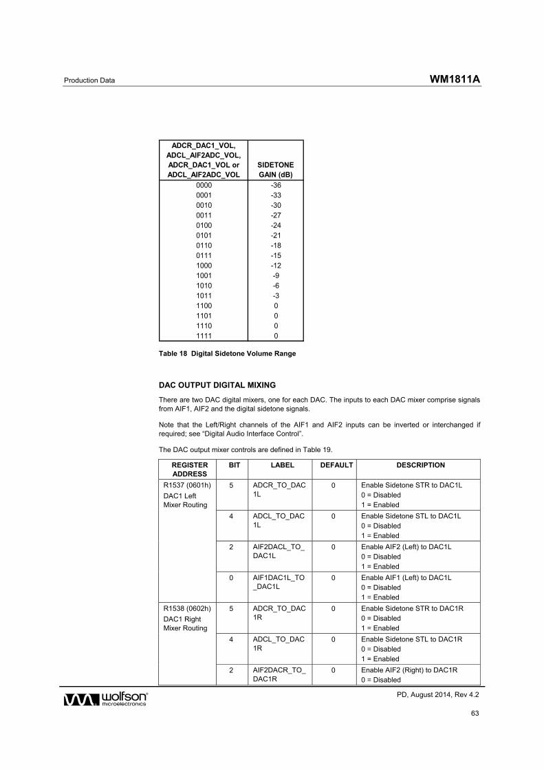
Production Data WM1811A
w PD, August 2014, Rev 4.2
63
ADCR_DAC1_VOL, ADCL_AIF2ADC_VOL, ADCR_DAC1_VOL or ADCL_AIF2ADC_VOL
SIDETONE GAIN (dB)
0000 -360001 -330010 -300011 -270100 -240101 -210110 -180111 -151000 -121001 -91010 -61011 -31100 01101 01110 01111 0
Table 18 Digital Sidetone Volume Range
DAC OUTPUT DIGITAL MIXING
There are two DAC digital mixers, one for each DAC. The inputs to each DAC mixer comprise signals from AIF1, AIF2 and the digital sidetone signals.
Note that the Left/Right channels of the AIF1 and AIF2 inputs can be inverted or interchanged if required; see “Digital Audio Interface Control”.
The DAC output mixer controls are defined in Table 19.
REGISTER ADDRESS
BIT LABEL DEFAULT DESCRIPTION
R1537 (0601h)
DAC1 Left Mixer Routing
5 ADCR_TO_DAC1L
0 Enable Sidetone STR to DAC1L 0 = Disabled 1 = Enabled
4 ADCL_TO_DAC1L
0 Enable Sidetone STL to DAC1L 0 = Disabled 1 = Enabled
2 AIF2DACL_TO_DAC1L
0 Enable AIF2 (Left) to DAC1L 0 = Disabled 1 = Enabled
0 AIF1DAC1L_TO_DAC1L
0 Enable AIF1 (Left) to DAC1L 0 = Disabled 1 = Enabled
R1538 (0602h)
DAC1 Right Mixer Routing
5 ADCR_TO_DAC1R
0 Enable Sidetone STR to DAC1R 0 = Disabled 1 = Enabled
4 ADCL_TO_DAC1R
0 Enable Sidetone STL to DAC1R 0 = Disabled 1 = Enabled
2 AIF2DACR_TO_DAC1R
0 Enable AIF2 (Right) to DAC1R 0 = Disabled
WM1811A Production Data
w PD, August 2014, Rev 4.2
64
REGISTER ADDRESS
BIT LABEL DEFAULT DESCRIPTION
1 = Enabled
0 AIF1DAC1R_TO_DAC1R
0 Enable AIF1 (Right) to DAC1R 0 = Disabled 1 = Enabled
Table 19 DAC Output Digital Mixing
AUDIO INTERFACE 2 (AIF2) OUTPUT DIGITAL MIXING
There are two digital mixers associated with the AIF2 output channels. The inputs to each AIF2 mixer comprise signals from AIF1, AIF2 and the digital sidetone signals.
Note that the Left/Right channels of the AIF1 and AIF2 inputs can be inverted or interchanged if required; see “Digital Audio Interface Control”.
The AIF2 output mixer controls are defined in Table 20.
REGISTER ADDRESS
BIT LABEL DEFAULT DESCRIPTION
R1540 (0604h)
AIF2ADC Left Mixer Routing
5 ADCR_TO_AIF2ADCL
0 Enable Sidetone STR to AIF2 Tx (Left)
0 = Disabled
1 = Enabled
4 ADCL_TO_AIF2ADCL
0 Enable Sidetone STL to AIF2 Tx (Left)
0 = Disabled
1 = Enabled
2 AIF2DACL_TO_AIF2ADCL
0 Enable AIF2 (Left) to AIF2 Tx (Left)
0 = Disabled
1 = Enabled
0 AIF1DAC1L_TO_AIF2ADCL
0 Enable AIF1 (Left) to AIF2 Tx (Left)
0 = Disabled
1 = Enabled
R1541 (0605h)
AIF2ADC Right Mixer Routing
5 ADCR_TO_AIF2ADCR
0 Enable Sidetone STR to AIF2 Tx (Right)
0 = Disabled
1 = Enabled
4 ADCL_TO_AIF2ADCR
0 Enable Sidetone STL to AIF2 Tx (Right)
0 = Disabled
1 = Enabled
2 AIF2DACR_TO_AIF2ADCR
0 Enable AIF2 (Right) to AIF2 Tx (Right)
0 = Disabled
1 = Enabled
0 AIF1DAC1R_TO_AIF2ADCR
0 Enable AIF1 (Right) to AIF2 Tx (Right)
0 = Disabled
1 = Enabled
Table 20 AIF2 Output Mixing

Production Data WM1811A
w PD, August 2014, Rev 4.2
65
DIGITAL VOLUME (DAC AND AIF2 OUTPUT PATHS)
The volume level of each DAC output mixer path and each AIF2 output mixer path can be controlled digitally over a range from -71.625dB to +12dBin 0.375dB steps. The level of attenuation for an eight-bit code X is given by:
0.375 (X-192) dB for 1 X 224; MUTE for X = 0; 12dB to 224 X 255
Each of the digital output mixer paths can be muted using the soft mute control bits described inTable 21. The WM1811A always applies a soft mute, where the volume is decreased gradually. The un-mute behaviour is configurable, as described in the “Digital Volume Soft Mute and Soft Un-Mute” section.
The DAC1_VU and AIF2TX_VU bits control the loading of digital volume control data. When DAC1_VU is set to 0, the DAC1L_VOL or DAC1R_VOL control data will be loaded into the respective control register, but will not actually change the digital gain setting. Both left and right gain settings are updated when a 1 is written to DAC1_VU. This makes it possible to update the gain of both channels simultaneously. A similar function for AIF2TXL and AIF2TXR is controlled by the AIF2TX_VU register bit.
REGISTER ADDRESS
BIT LABEL DEFAULT DESCRIPTION
R1552 (0610h)
DAC1 Left Volume
9 DAC1L_MUTE
1 DAC1L Soft Mute Control
0 = DAC Un-mute
1 = DAC Mute
8 DAC1_VU N/A DAC1L and DAC1R Volume Update
Writing a 1 to this bit will cause the DAC1L and DAC1R volume to be updated simultaneously
7:0 DAC1L_VOL [7:0]
C0h
(0dB)
DAC1L Digital Volume
00h = MUTE
01h = -71.625dB
… (0.375dB steps)
C0h = 0dB
… (0.375dB steps)
E0h = 12dB
FFh = 12dB
(See Table 22for volume range)
R1553 (0611h)
DAC1 Right Volume
9 DAC1R_MUTE
1 DAC1R Soft Mute Control
0 = DAC Un-mute
1 = DAC Mute
8 DAC1_VU N/A DAC1L and DAC1R Volume Update
Writing a 1 to this bit will cause the DAC1L and DAC1R volume to be updated simultaneously
7:0 DAC1R_VOL [7:0]
C0h
(0dB)
DAC1R Digital Volume
00h = MUTE
01h = -71.625dB
… (0.375dB steps)
C0h = 0dB
… (0.375dB steps)
E0h = 12dB
FFh = 12dB
(See Table 22for volume range)
R1554 (0612h)
AIF2TX Left Volume
9 AIF2TXL_MUTE
1 AIF2 Tx (Left) Soft Mute Control
0 = Un-mute
1 = Mute

WM1811A Production Data
w PD, August 2014, Rev 4.2
66
REGISTER ADDRESS
BIT LABEL DEFAULT DESCRIPTION
8 AIF2TX_VU N/A AIF2 Tx (Left) and AIF2 Tx (Right) Volume Update
Writing a 1 to this bit will cause the AIF2TXL and AIF2TXR volume to be updated simultaneously
7:0 AIF2TXL_VOL [7:0]
C0h
(0dB)
AIF2 Tx (Left) Volume Digital Volume
00h = MUTE
01h = -71.625dB
… (0.375dB steps)
C0h = 0dB
… (0.375dB steps)
E0h = 12dB
FFh = 12dB
(See Table 22for volume range)
R1555 (0613h)
AIF2TX Right Volume
9 AIF2TXR_MUTE
1 AIF2 Tx (Right) Soft Mute Control
0 = DAC Un-mute
1 = DAC Mute
8 AIF2TX_VU N/A AIF2 Tx (Left) and AIF2 Tx (Right) Volume Update
Writing a 1 to this bit will cause the AIF2TXL and AIF2TXR volume to be updated simultaneously
7:0 AIF2TXR_VOL [7:0]
C0h
(0dB)
AIF2 Tx (Right) Digital Volume
00h = MUTE
01h = -71.625dB
… (0.375dB steps)
C0h = 0dB
… (0.375dB steps)
E0h = 12dB
FFh = 12dB
(See Table 22for volume range)
Table 21 DAC and AIF2 Output Digital Volume Control

Production Data WM1811A
w PD, August 2014, Rev 4.2
67
DAC / AIF2 Tx Volume
Volume (dB)
DAC / AIF2 Tx Volume
Volume (dB)
DAC / AIF2 Tx Volume
Volume (dB)
DAC / AIF2 Tx Volume
Volume (dB)
0h MUTE 40h -48.000 80h -24.000 C0h 0.000
1h -71.625 41h -47.625 81h -23.625 C1h 0.375
2h -71.250 42h -47.250 82h -23.250 C2h 0.750
3h -70.875 43h -46.875 83h -22.875 C3h 1.125
4h -70.500 44h -46.500 84h -22.500 C4h 1.500
5h -70.125 45h -46.125 85h -22.125 C5h 1.875
6h -69.750 46h -45.750 86h -21.750 C6h 2.250
7h -69.375 47h -45.375 87h -21.375 C7h 2.625
8h -69.000 48h -45.000 88h -21.000 C8h 3.000
9h -68.625 49h -44.625 89h -20.625 C9h 3.375
Ah -68.250 4Ah -44.250 8Ah -20.250 CAh 3.750
Bh -67.875 4Bh -43.875 8Bh -19.875 CBh 4.125
Ch -67.500 4Ch -43.500 8Ch -19.500 CCh 4.500
Dh -67.125 4Dh -43.125 8Dh -19.125 CDh 4.875
Eh -66.750 4Eh -42.750 8Eh -18.750 CEh 5.250
Fh -66.375 4Fh -42.375 8Fh -18.375 CFh 5.625
10h -66.000 50h -42.000 90h -18.000 D0h 6.000
11h -65.625 51h -41.625 91h -17.625 D1h 6.375
12h -65.250 52h -41.250 92h -17.250 D2h 6.750
13h -64.875 53h -40.875 93h -16.875 D3h 7.125
14h -64.500 54h -40.500 94h -16.500 D4h 7.500
15h -64.125 55h -40.125 95h -16.125 D5h 7.875
16h -63.750 56h -39.750 96h -15.750 D6h 8.250
17h -63.375 57h -39.375 97h -15.375 D7h 8.625
18h -63.000 58h -39.000 98h -15.000 D8h 9.000
19h -62.625 59h -38.625 99h -14.625 D9h 9.375
1Ah -62.250 5Ah -38.250 9Ah -14.250 DAh 9.750
1Bh -61.875 5Bh -37.875 9Bh -13.875 DBh 10.125
1Ch -61.500 5Ch -37.500 9Ch -13.500 DCh 10.500
1Dh -61.125 5Dh -37.125 9Dh -13.125 DDh 10.875
1Eh -60.750 5Eh -36.750 9Eh -12.750 DEh 11.250
1Fh -60.375 5Fh -36.375 9Fh -12.375 DFh 11.625
20h -60.000 60h -36.000 A0h -12.000 E0h 12.000
21h -59.625 61h -35.625 A1h -11.625 E1h 12.000
22h -59.250 62h -35.250 A2h -11.250 E2h 12.000
23h -58.875 63h -34.875 A3h -10.875 E3h 12.000
24h -58.500 64h -34.500 A4h -10.500 E4h 12.000
25h -58.125 65h -34.125 A5h -10.125 E5h 12.000
26h -57.750 66h -33.750 A6h -9.750 E6h 12.000
27h -57.375 67h -33.375 A7h -9.375 E7h 12.000
28h -57.000 68h -33.000 A8h -9.000 E8h 12.000
29h -56.625 69h -32.625 A9h -8.625 E9h 12.000
2Ah -56.250 6Ah -32.250 AAh -8.250 EAh 12.000
2Bh -55.875 6Bh -31.875 ABh -7.875 EBh 12.000
2Ch -55.500 6Ch -31.500 ACh -7.500 ECh 12.000
2Dh -55.125 6Dh -31.125 ADh -7.125 EDh 12.000
2Eh -54.750 6Eh -30.750 AEh -6.750 EEh 12.000
2Fh -54.375 6Fh -30.375 AFh -6.375 EFh 12.000
30h -54.000 70h -30.000 B0h -6.000 F0h 12.000
31h -53.625 71h -29.625 B1h -5.625 F1h 12.000
32h -53.250 72h -29.250 B2h -5.250 F2h 12.000
33h -52.875 73h -28.875 B3h -4.875 F3h 12.000
34h -52.500 74h -28.500 B4h -4.500 F4h 12.000
35h -52.125 75h -28.125 B5h -4.125 F5h 12.000
36h -51.750 76h -27.750 B6h -3.750 F6h 12.000
37h -51.375 77h -27.375 B7h -3.375 F7h 12.000
38h -51.000 78h -27.000 B8h -3.000 F8h 12.000
39h -50.625 79h -26.625 B9h -2.625 F9h 12.000
3Ah -50.250 7Ah -26.250 BAh -2.250 FAh 12.000
3Bh -49.875 7Bh -25.875 BBh -1.875 FBh 12.000
3Ch -49.500 7Ch -25.500 BCh -1.500 FCh 12.000
3Dh -49.125 7Dh -25.125 BDh -1.125 FDh 12.000
3Eh -48.750 7Eh -24.750 BEh -0.750 FEh 12.000
3Fh -48.375 7Fh -24.375 BFh -0.375 FFh 12.000
Table 22 DAC and AIF2 Output Digital Volume Range

WM1811A Production Data
w PD, August 2014, Rev 4.2
68
DIGITAL VOLUME SOFT MUTE AND SOFT UN-MUTE
The WM1811A has a soft mute function which ensures that a gradual attenuation is applied to the DAC output mixers or AIF2 output mixers when the associated mute is asserted. The soft mute rate can be selected using the DAC_MUTERATE bit.
When a mute bit is disabled, the gain will either gradually ramp back up to the digital gain setting, or return instantly to the digital gain setting, depending on the DAC_SOFTMUTEMODE register bit. If the gradual un-mute ramp is selected (DAC_SOFTMUTEMODE = 1), then the un-mute rate is determined by the DAC_MUTERATE bit.
Note that each DAC (or AIF2 output mixer) is soft-muted by default. To play back an audio signal, the mute must first be disabled by setting the applicable mute control to 0 (seeTable 21).
Soft Mute Mode would typically be enabled (DAC_SOFTMUTEMODE = 1) when using mute during playback of audio data so that when the mute is subsequently disabled, the volume increase will not create pop noise by jumping immediately to the previous volume level (e.g. resuming playback after pausing during a track).
Soft Mute Mode would typically be disabled (DAC_SOFTMUTEMODE = 0) when un-muting at the start of a music file, in order that the first part of the track is not attenuated (e.g. when starting playback of a new track, or resuming playback after pausing between tracks).
The DAC soft-mute function is illustrated in Figure 19 for DAC1L and DAC1R. The same function is applicable to AIF2TXL and AIF2TXRalso.
= 00000000 = [non-zero]
DAC1L_MUTE = 0DAC1R_MUTE = 0
DAC1L_MUTE = 1DAC1R_MUTE = 1
DAC1L_MUTE = 0DAC1R_MUTE = 0
DAC1L_MUTE = 0DAC1R_MUTE = 0
DAC1L_MUTE = 1DAC1R_MUTE = 1
DAC1L_MUTE = 0DAC1R_MUTE = 0
DAC1L_VOL or DAC1R_VOL = [non-zero]
DAC_SOFTMUTEMODE = 0
DAC_SOFTMUTEMODE = 1
DAC muting and un-muting using volume control bits DAC1L_VOL and DAC1R_VOL
DAC muting and un-muting using soft mute bits DAC1L_MUTE or DAC1R_MUTE
Soft mute mode not enabled (DAC_SOFTMUTEMODE = 0).
DAC muting and un-muting using soft mute bit DAC_MUTE.
Soft mute mode enabled (DAC_SOFTMUTEMODE = 1).
Figure 19 Digital Volume Soft Mute Control
The DAC Soft Mute register controls are defined in Table 23.
The volume ramp rate during soft mute and un-mute is controlled by the DAC_MUTERATE bit. Ramp rates of fs/32 and fs/2 are selectable. The ramp rate determines the rate at which the volume will be increased or decreased. Note that the actual ramp time depends on the extent of the difference between the muted and un-muted volume settings.

Production Data WM1811A
w PD, August 2014, Rev 4.2
69
REGISTER ADDRESS
BIT LABEL DEFAULT DESCRIPTION
R1556 (0614h)
DAC Softmute
1 DAC_SOFTMUTEMODE
0 DAC/AIF2 Digital Output Mixer Unmute Ramp select
0 = Unmuting the DAC / AIF2 volume will immediately apply the DAC1[L/R]_VOLor AIF2TX[L/R]_VOL settings.
1 = Unmuting the DAC / AIF2 volume will cause a gradual ramp up to the DAC1[L/R]_VOLor AIF2TX[L/R]_VOL settings.
0 DAC_MUTERATE
0 DAC/AIF2 Digital Output Mixer Soft Mute Ramp Rate
0 = Fast ramp (fs/2, maximum ramp time is 10.7ms at fs=48k)
1 = Slow ramp (fs/32, maximum ramp time is 171ms at fs=48k)
(Note: ramp rate scales with sample rate.)
Table 23 Digital Volume Soft-Mute Control
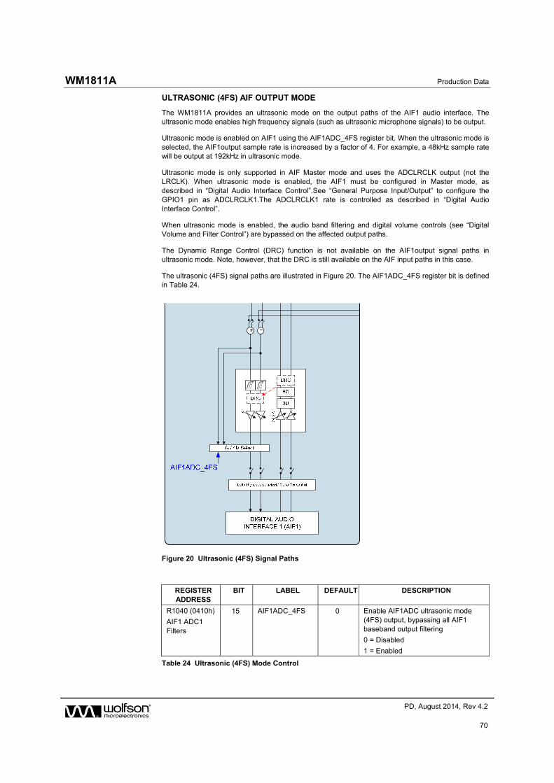
WM1811A Production Data
w PD, August 2014, Rev 4.2
70
ULTRASONIC (4FS) AIF OUTPUT MODE
The WM1811A provides an ultrasonic mode on the output paths of the AIF1 audio interface. The ultrasonic mode enables high frequency signals (such as ultrasonic microphone signals) to be output.
Ultrasonic mode is enabled on AIF1 using the AIF1ADC_4FS register bit. When the ultrasonic mode is selected, the AIF1output sample rate is increased by a factor of 4. For example, a 48kHz sample rate will be output at 192kHz in ultrasonic mode.
Ultrasonic mode is only supported in AIF Master mode and uses the ADCLRCLK output (not the LRCLK). When ultrasonic mode is enabled, the AIF1 must be configured in Master mode, as described in “Digital Audio Interface Control”.See “General Purpose Input/Output” to configure the GPIO1 pin as ADCLRCLK1.The ADCLRCLK1 rate is controlled as described in “Digital Audio Interface Control”.
When ultrasonic mode is enabled, the audio band filtering and digital volume controls (see “Digital Volume and Filter Control”) are bypassed on the affected output paths.
The Dynamic Range Control (DRC) function is not available on the AIF1output signal paths in ultrasonic mode. Note, however, that the DRC is still available on the AIF input paths in this case.
The ultrasonic (4FS) signal paths are illustrated in Figure 20. The AIF1ADC_4FS register bit is defined in Table 24.
Figure 20 Ultrasonic (4FS) Signal Paths
REGISTER ADDRESS
BIT LABEL DEFAULT DESCRIPTION
R1040 (0410h)
AIF1 ADC1 Filters
15 AIF1ADC_4FS 0 Enable AIF1ADC ultrasonic mode (4FS) output, bypassing all AIF1 baseband output filtering
0 = Disabled
1 = Enabled
Table 24 Ultrasonic (4FS) Mode Control

Production Data WM1811A
w PD, August 2014, Rev 4.2
71
DYNAMIC RANGE CONTROL (DRC)
The Dynamic Range Control (DRC) is a circuit which can be enabled in the digital playback or digital record paths of the WM1811A audio interfaces. The function of the DRC is to adjust the signal gain in conditions where the input amplitude is unknown or varies over a wide range, e.g. when recording from microphones built into a handheld system.
The DRC can apply Compression and Automatic Level Control to the signal path. It incorporates ‘anti-clip’ and ‘quick release’ features for handling transients in order to improve intelligibility in the presence of loud impulsive noises.
The DRC also incorporates a Noise Gate function, which provides additional attenuation of very low-level input signals. This means that the signal path is quiet when no signal is present, giving an improvement in background noise level under these conditions.
The WM1811A provides two stereo Dynamic Range Controllers (DRCs); these are associated with AIF1 and AIF2 respectively. Each DRC can be enabled either in the DAC playback (AIF input) path or in the ADC record (AIF output) path, as described in the “Digital Core Architecture” section.
The DRCs are enabled in the DAC or ADCs audio signal paths using the register bits described in Table 25. Note that enabling any DRC in the DAC and ADC paths simultaneously is an invalid selection.
When the DRC is enabled in any of the ADC (digital record) paths, the associated High Pass Filter (HPF) must be enabled also; this ensures that DC offsets are removed prior to the DRC processing. The output path HPF control registers are described in Table 37 (for AIF1 output paths) and Table 45 (for AIF2 output paths). These are described in the “Digital Volume and Filter Control” section.
Note that, when ultrasonic (4FS) mode is selected on AIF1, then the DRC function is bypassed on the respective ADC (output) signal paths. The DRC may still be selected on the AIF1DAC (input) signal paths.
REGISTER ADDRESS
BIT LABEL DEFAULT DESCRIPTION
R1088 (0440h)
AIF1DRC1 (1)
2 AIF1DAC1_DRC_ENA
0 Enable DRC in AIF1DAC playback path
0 = Disabled
1 = Enabled
1 AIF1ADC1L_DRC_ENA
0 Enable DRC in AIF1ADC (Left) record path
0 = Disabled
1 = Enabled
0 AIF1ADC1R_DRC_ENA
0 Enable DRC in AIF1ADC (Right) record path
0 = Disabled
1 = Enabled
R1344 (0540h)
AIF2DRC (1)
2 AIF2DAC_DRC_ENA
0 Enable DRC in AIF2DAC playback path
0 = Disabled
1 = Enabled
1 AIF2ADCL_DRC_ENA
0 Enable DRC in AIF2ADC (Left) record path
0 = Disabled
1 = Enabled
0 AIF2ADCR_DRC_ENA
0 Enable DRC in AIF2ADC (Right) record path
0 = Disabled
1 = Enabled
Table 25 DRC Enable

WM1811A Production Data
w PD, August 2014, Rev 4.2
72
The following description of the DRC is applicable to both DRCs. The associated register control fields are described inTable 27 and Table 28 for the respective DRCs.
Note that, wherethe following description refers to register names, the generic prefix [DRC] is quoted:
For the DRC associated with AIF1, [DRC] = AIF1DRC1.
For the DRC associated with AIF2, [DRC] = AIF2DRC.
DRC COMPRESSION / EXPANSION /LIMITING
The DRC supports two different compression regions, separated by a “Knee” at a specific input amplitude. In the region above the knee, the compression slope [DRC]_HI_COMP applies; in the region below the knee, the compression slope [DRC]_LO_COMP applies.
The DRC also supports a noise gate region, where low-level input signals are heavily attenuated. This function can be enabled or disabled according to the application requirements. The DRC response in this region is defined by the expansion slope [DRC]_NG_EXP.
For additional attenuation of signals in the noise gate region, an additional “knee” can be defined (shown as “Knee2” in Figure 21). When this knee is enabled, this introduces an infinitely steep drop-off in the DRC response pattern between the [DRC]_LO_COMP and [DRC]_NG_EXP regions.
The overall DRC compression characteristic in “steady state” (i.e. where the input amplitude is near-constant) is illustrated in Figure 21.
Figure 21 DRC Response Characteristic
The slope of the DRC response is determined by register fields [DRC]_HI_COMP and [DRC]_LO_COMP. A slope of 1 indicates constant gain in this region. A slope less than 1 represents compression (i.e. a change in input amplitude produces only a smaller change in output amplitude). A slope of 0 indicates that the target output amplitude is the same across a range of input amplitudes; this is infinite compression.
When the noise gate is enabled, the DRC response in this region is determined by the [DRC]_NG_EXP register. A slope of 1 indicates constant gain in this region. A slope greater than 1 represents expansion (ie. a change in input amplitude produces a larger change in output amplitude).
When the DRC_KNEE2_OP knee is enabled (“Knee2” in Figure 21), this introduces the vertical line in the response pattern illustrated, resulting in infinitely steep attenuation at this point in the response.

Production Data WM1811A
w PD, August 2014, Rev 4.2
73
The DRC parameters are listed in Table 26.
REF PARAMETER DESCRIPTION
1 [DRC]_KNEE_IP Input level at Knee1 (dB)
2 [DRC]_KNEE_OP Output level at Knee2 (dB)
3 [DRC]_HI_COMP Compression ratio above Knee1
4 [DRC]_LO_COMP Compression ratio below Knee1
5 [DRC]_KNEE2_IP Input level at Knee2 (dB)
6 [DRC]_NG_EXP Expansion ratio below Knee2
7 [DRC]_KNEE2_OP Output level at Knee2 (dB)
Table 26 DRC Response Parameters
The noise gate is enabled when the [DRC]_NG_ENA register is set. When the noise gate is not enabled, parameters 5, 6, 7 above are ignored, and the [DRC]_LO_COMP slope applies to all input signal levels below Knee1.
The DRC_KNEE2_OP knee is enabled when the [DRC]_KNEE2_OP_ENA register is set. When this bit is not set, then parameter 7 above is ignored, and the Knee2 position always coincides with the low end of the [DRC]_LO_COMP region.
The “Knee1” point in Figure 21 is determined by register fields [DRC]_KNEE_IP and [DRC]_KNEE_OP.
Parameter Y0, the output level for a 0dB input, is not specified directly, but can be calculated from the other parameters, using the equation:
GAIN LIMITS
The minimum and maximum gain applied by the DRC is set by register fields [DRC]_MINGAIN, [DRC]_MAXGAIN and [DRC]_NG_MINGAIN. These limits can be used to alter the DRC response from that illustrated in Figure 21. If the range between maximum and minimum gain is reduced, then the extent of the dynamic range control is reduced.
The minimum gain in the Compression regions of the DRC response is set by [DRC]_MINGAIN. The mimimum gain in the Noise Gate region is set by [DRC]_NG_MINGAIN. The minimum gain limit prevents excessive attenuation of the signal path.
The maximum gain limit set by [DRC]_MAXGAIN prevents quiet signals (or silence) from being excessively amplified.

WM1811A Production Data
w PD, August 2014, Rev 4.2
74
DYNAMIC CHARACTERISTICS
The dynamic behaviour determines how quickly the DRC responds to changing signal levels. Note that the DRC responds to the average (RMS) signal amplitude over a period of time.
The [DRC]_ATK determines how quickly the DRC gain decreases when the signal amplitude is high. The [DRC]_DCY determines how quickly the DRC gain increases when the signal amplitude is low.
These register fields are described in Table 27 and Table 28. Note that the register defaults are suitable for general purpose microphone use.
ANTI-CLIP CONTROL
The DRC includes an Anti-Clip feature to avoid signal clipping when the input amplitude rises very quickly. This feature uses a feed-forward technique for early detection of a rising signal level. Signal clipping is avoided by dynamically increasing the gain attack rate when required. The Anti-Clip feature is enabled using the [DRC]_ANTICLIP bit.
Note that the feed-forward processing increases the latency in the input signal path.
Note that the Anti-Clip feature operates entirely in the digital domain. It cannot be used to prevent signal clipping in the analogue domain nor in the source signal. Analogue clipping can only be prevented by reducing the analogue signal gain or by adjusting the source signal.
Note that the Anti-Clip feature should not be enabled at the same time as the Quick Release feature (described below) on the same DRC.
QUICK RELEASE CONTROL
The DRC includes a Quick-Release feature to handle short transient peaks that are not related to the intended source signal. For example, in handheld microphone recording, transient signal peaks sometimes occur due to user handling, key presses or accidental tapping against the microphone. The Quick Release feature ensures that these transients do not cause the intended signal to be masked by the longer time constants of [DRC]_DCY.
The Quick-Release feature is enabled by setting the [DRC]_QR bit. When this bit is enabled, the DRC measures the crest factor (peak to RMS ratio) of the input signal. A high crest factor is indicative of a transient peak that may not be related to the intended source signal. If the crest factor exceeds the level set by [DRC]_QR_THR, then the normal decay rate ([DRC]_DCY) is ignored and a faster decay rate ([DRC]_QR_DCY) is used instead.
Note that the Quick Release feature should not be enabled at the same time as the Anti-Clip feature (described above) on the same DRC.
SIGNAL ACTIVITY DETECT
The DRC incorporates a configurable signal detect function, allowing the signal level at the DRC input to be monitored and to be used to trigger other events. This can be used to detect the presence of a microphone signal on an ADC or digital mic channel, or can be used to detect an audio signal received over the digital audio interface.
The Peak signal level or the RMS signal level of the DRC input can be selected as the detection threshold. When the threshold condition is exceeded, an interrupt or GPIO output can be generated. See “General Purpose Input/Output” for a full description of the applicable control fields.

Production Data WM1811A
w PD, August 2014, Rev 4.2
75
DRC REGISTER CONTROLS
The AIF1DRC control registers are described in Table 27.
The AIF2DRC control registers are described in Table 28.
REGISTER ADDRESS
BIT LABEL DEFAULT DESCRIPTION
R1088(0440h)
AIF1 DRC1 (1)
8 AIF1DRC1_NG_ENA
0 AIF1 DRC Noise Gate Enable
0 = Disabled
1 = Enabled
5 AIF1DRC1_KNEE2_OP_ENA
0 AIF1 DRCKNEE2_OP Enable
0 = Disabled
1 = Enabled
4 AIF1DRC1_QR 1 AIF1 DRC Quick-release Enable
0 = Disabled
1 = Enabled
3 AIF1DRC1_ANTICLIP
1 AIF1 DRC Anti-clip Enable
0 = Disabled
1 = Enabled
R1089(0441h)
AIF1 DRC1 (2)
12:9 AIF1DRC1_ATK [3:0]
0100 AIF1 DRC Gain attack rate (seconds/6dB)
0000 = Reserved
0001 = 181us
0010 = 363us
0011 = 726us
0100 = 1.45ms
0101 = 2.9ms
0110 = 5.8ms
0111 = 11.6ms
1000 = 23.2ms
1001 = 46.4ms
1010 = 92.8ms
1011 = 185.6ms
1100-1111 = Reserved
8:5 AIF1DRC1_DCY [3:0]
0010 AIF1 DRC Gain decay rate (seconds/6dB)
0000 = 186ms
0001 = 372ms
0010 = 743ms
0011 = 1.49s
0100 = 2.97s
0101 = 5.94s
0110 = 11.89s
0111 = 23.78s
1000 = 47.56s
1001-1111 = Reserved
4:2 AIF1DRC1_MINGAIN [2:0]
001 AIF1 DRC Minimum gain to attenuate audio signals
000 = 0dB
001 = -12dB (default)
010 = -18dB
011 = -24dB
100 = -36dB
101 = Reserved
11X = Reserved

WM1811A Production Data
w PD, August 2014, Rev 4.2
76
REGISTER ADDRESS
BIT LABEL DEFAULT DESCRIPTION
1:0 AIF1DRC1_MAXGAIN [1:0]
01 AIF1 DRC Maximum gain to boost audio signals (dB)
00 = 12dB
01 = 18dB
10 = 24dB
11 = 36dB
R1090(0442h)
AIF1 DRC1 (3)
15:12 AIF1DRC1_NG_MINGAIN [3:0]
0000 AIF1 DRC Minimum gain to attenuate audio signals when the noise gate is active.
0000 = -36dB
0001 = -30dB
0010 = -24dB
0011 = -18dB
0100 = -12dB
0101 = -6dB
0110 = 0dB
0111 = 6dB
1000 = 12dB
1001 = 18dB
1010 = 24dB
1011 = 30dB
1100 = 36dB
1101 to 1111 = Reserved
11:10 AIF1DRC1_NG_EXP [1:0]
00 AIF1 DRC Noise Gate slope
00 = 1 (no expansion)
01 = 2
10 = 4
11 = 8
9:8 AIF1DRC1_QR_THR [1:0]
00 AIF1 DRC Quick-release threshold (crest factor in dB)
00 = 12dB
01 = 18dB
10 = 24dB
11 = 30dB
7:6 AIF1DRC1_QR_DCY [1:0]
00 AIF1 DRC Quick-release decay rate (seconds/6dB)
00 = 0.725ms
01 = 1.45ms
10 = 5.8ms
11 = Reserved
5:3 AIF1DRC1_HI_COMP [2:0]
000 AIF1 DRC Compressor slope (upper region)
000 = 1 (no compression)
001 = 1/2
010 = 1/4
011 = 1/8
100 = 1/16
101 = 0
110 = Reserved
111 = Reserved

Production Data WM1811A
w PD, August 2014, Rev 4.2
77
REGISTER ADDRESS
BIT LABEL DEFAULT DESCRIPTION
2:0 AIF1DRC1_LO_COMP [2:0]
000 AIF1 DRC Compressor slope (lower region)
000 = 1 (no compression)
001 = 1/2
010 = 1/4
011 = 1/8
100 = 0
101 = Reserved
11X = Reserved
R1091(0443h)
AIF1 DRC1 (4)
10:5 AIF1DRC1_KNEE_IP [5:0]
000000 AIF1 DRC Input signal level at the Compressor ‘Knee’.
000000 = 0dB
000001 = -0.75dB
000010 = -1.5dB
… (-0.75dB steps)
111100 = -45dB
111101 = Reserved
11111X = Reserved
4:0 AIF1DRC1_KNEE_OP [4:0]
00000 AIF1 DRC Output signal at the Compressor ‘Knee’.
00000 = 0dB
00001 = -0.75dB
00010 = -1.5dB
… (-0.75dB steps)
11110 = -22.5dB
11111 = Reserved
R1092(0444h)
AIF1 DRC1 (5)
9:5 AIF1DRC1_KNEE2_IP [4:0]
00000 AIF1 DRC Input signal level at the Noise Gate threshold ‘Knee2’.
00000 = -36dB
00001 = -37.5dB
00010 = -39dB
… (-1.5dB steps)
11110 = -81dB
11111 = -82.5dB
Only applicable when AIF1DRC1_NG_ENA = 1.
4:0 AIF1DRC1_KNEE2_OP [4:0]
00000 AIF1 DRC Output signal at the Noise Gate threshold ‘Knee2’.
00000 = -30dB
00001 = -31.5dB
00010 = -33dB
… (-1.5dB steps)
11110 = -75dB
11111 = -76.5dB
Only applicable when AIF1DRC1_KNEE2_OP_ENA = 1.
Table 27 AIF1 DRC Controls

WM1811A Production Data
w PD, August 2014, Rev 4.2
78
REGISTER ADDRESS
BIT LABEL DEFAULT DESCRIPTION
R1344 (0540h)
AIF2DRC (1)
8 AIF2DRC_NG_ENA
0 AIF2 DRC Noise Gate Enable
0 = Disabled
1 = Enabled
5 AIF2DRC_KNEE2_OP_ENA
0 AIF2 DRCKNEE2_OP Enable
0 = Disabled
1 = Enabled
4 AIF2DRC_QR 1 AIF2 DRC Quick-release Enable
0 = Disabled
1 = Enabled
3 AIF2DRC_ANTICLIP
1 AIF2 DRC Anti-clip Enable
0 = Disabled
1 = Enabled
R1345 (0541h)
AIF2DRC (2)
12:9 AIF2DRC_ATK [3:0]
0100 AIF2 DRC Gain attack rate (seconds/6dB)
0000 = Reserved
0001 = 181us
0010 = 363us
0011 = 726us
0100 = 1.45ms
0101 = 2.9ms
0110 = 5.8ms
0111 = 11.6ms
1000 = 23.2ms
1001 = 46.4ms
1010 = 92.8ms
1011 = 185.6ms
1100-1111 = Reserved
8:5 AIF2DRC_DCY [3:0]
0010 AIF2 DRC Gain decay rate (seconds/6dB)
0000 = 186ms
0001 = 372ms
0010 = 743ms
0011 = 1.49s
0100 = 2.97s
0101 = 5.94s
0110 = 11.89s
0111 = 23.78s
1000 = 47.56s
1001-1111 = Reserved
4:2 AIF2DRC_MINGAIN [2:0]
001 AIF2 DRC Minimum gain to attenuate audio signals
000 = 0dB
001 = -12dB (default)
010 = -18dB
011 = -24dB
100 = -36dB
101 = Reserved
11X = Reserved

Production Data WM1811A
w PD, August 2014, Rev 4.2
79
REGISTER ADDRESS
BIT LABEL DEFAULT DESCRIPTION
1:0 AIF2DRC_MAXGAIN [1:0]
01 AIF2 DRC Maximum gain to boost audio signals (dB)
00 = 12dB
01 = 18dB
10 = 24dB
11 = 36dB
R1346 (0542h)
AIF2DRC (3)
15:12 AIF2DRC_NG_MINGAIN [3:0]
0000 AIF2 DRC Minimum gain to attenuate audio signals when the noise gate is active.
0000 = -36dB
0001 = -30dB
0010 = -24dB
0011 = -18dB
0100 = -12dB
0101 = -6dB
0110 = 0dB
0111 = 6dB
1000 = 12dB
1001 = 18dB
1010 = 24dB
1011 = 30dB
1100 = 36dB
1101 to 1111 = Reserved
11:10 AIF2DRC_NG_EXP [1:0]
00 AIF2 DRC Noise Gate slope
00 = 1 (no expansion)
01 = 2
10 = 4
11 = 8
9:8 AIF2DRC_QR_THR [1:0]
00 AIF2 DRC Quick-release threshold (crest factor in dB)
00 = 12dB
01 = 18dB
10 = 24dB
11 = 30dB
7:6 AIF2DRC_QR_DCY [1:0]
00 AIF2 DRC Quick-release decay rate (seconds/6dB)
00 = 0.725ms
01 = 1.45ms
10 = 5.8ms
11 = Reserved
5:3 AIF2DRC_HI_COMP [2:0]
000 AIF2 DRC Compressor slope (upper region)
000 = 1 (no compression)
001 = 1/2
010 = 1/4
011 = 1/8
100 = 1/16
101 = 0
110 = Reserved
111 = Reserved

WM1811A Production Data
w PD, August 2014, Rev 4.2
80
REGISTER ADDRESS
BIT LABEL DEFAULT DESCRIPTION
2:0 AIF2DRC_LO_COMP [2:0]
000 AIF2 DRC Compressor slope (lower region)
000 = 1 (no compression)
001 = 1/2
010 = 1/4
011 = 1/8
100 = 0
101 = Reserved
11X = Reserved
R1347 (0543h)
AIF2DRC (4)
10:5 AIF2DRC_KNEE_IP [5:0]
000000 AIF2 DRC Input signal level at the Compressor ‘Knee’.
000000 = 0dB
000001 = -0.75dB
000010 = -1.5dB
… (-0.75dB steps)
111100 = -45dB
111101 = Reserved
11111X = Reserved
4:0 AIF2DRC_KNEE_OP [4:0]
00000 AIF2 DRC Output signal at the Compressor ‘Knee’.
00000 = 0dB
00001 = -0.75dB
00010 = -1.5dB
… (-0.75dB steps)
11110 = -22.5dB
11111 = Reserved
R1348 (0544h)
AIF2DRC (5)
9:5 AIF2DRC_KNEE2_IP [4:0]
00000 AIF2 DRC Input signal level at the Noise Gate threshold ‘Knee2’.
00000 = -36dB
00001 = -37.5dB
00010 = -39dB
… (-1.5dB steps)
11110 = -81dB
11111 = -82.5dB
Only applicable when AIF2DRC_NG_ENA = 1.
4:0 AIF2DRC_KNEE2_OP [4:0]
00000 AIF2 DRC Output signal at the Noise Gate threshold ‘Knee2’.
00000 = -30dB
00001 = -31.5dB
00010 = -33dB
… (-1.5dB steps)
11110 = -75dB
11111 = -76.5dB
Only applicable when AIF2DRC_KNEE2_OP_ENA = 1.
Table 28 AIF2 DRC Controls

Production Data WM1811A
w PD, August 2014, Rev 4.2
81
RETUNETM MOBILE PARAMETRIC EQUALIZER (EQ)
The ReTuneTM Mobile Parametric EQ is a circuit which can be enabled in the digital playback path of the WM1811A audio interfaces. The function of the EQ is to adjust the frequency characteristic of the output in order to compensate for unwanted frequency characteristics in the loudspeaker (or other output transducer). It can also be used to tailor the response according to user preferences, for example to accentuate or attenuate specific frequency bands to emulate different sound profiles or environments e.g. concert hall, rock etc.
The WM1811A provides two stereo EQ circuits; these are associated with AIF1 and AIF2 respectively. The EQ is enabled in these signal paths using the register bits described in Table 29.
REGISTER ADDRESS
BIT LABEL DEFAULT DESCRIPTION
R1152 (0480h)
AIF1 DAC1 EQ Gains (1)
0 AIF1DAC1_EQ_ENA
0 Enable EQ in AIF1DAC playback path
0 = Disabled
1 = Enabled
R1408 (0580h)
AIF2 EQ Gains (1)
0 AIF2DAC_EQ_ENA
0 Enable EQ in AIF2DAC playback path
0 = Disabled
1 = Enabled
Table 29 ReTuneTM Mobile Parametric EQ Enable
The following description of the EQ is applicable to both EQ circuits. The associated register control fields are described in Table 31 and Table 32 for the respective EQs. The EQ provides selective control of 5 frequency bands as described below.
The low frequency band (Band 1) filter can be configured either as a peak filter or a shelving filter. When configured as a shelving filter, is provides adjustable gain below the Band 1 cut-off frequency. As a peak filter, it provides adjustable gain within a defined frequency band that is centred on the Band 1 frequency.
The mid frequency bands (Band 2, Band 3, Band 4) filters are peak filters, which provide adjustable gain around the respective centre frequency.
The high frequency band (Band 5) filter is a shelving filter, which provides adjustable gain above the Band 5 cut-off frequency.
The EQ can be configured to operate in two modes - “Default” mode or “ReTuneTM Mobile” mode.The associated register control fields are described in Table 31 and Table 32 for the respective EQs.
DEFAULT MODE (5-BAND PARAMETRIC EQ)
In default mode, the cut-off/centre frequencies are fixed as per Table 30. The filter bandwidths are also fixed in default mode. The gain of the individual bands (-12dB to +12dB) can be controlled as described in Table 31.
The cut-off / centre frequencies noted in Table 30 are applicable to a sample rate of 48kHz. When using other sample rates, these frequencies will be scaled in proportion to the selected sample rate for the associated Audio Interface (AIF1 or AIF2).
If AIF1 and AIF2 are operating at different sample rates, then the cut-off / centre frequencies will be different for the two interfaces. Note that the frequencies can be set to other values by using the features described in “ReTuneTM Mobile Mode”.

WM1811A Production Data
w PD, August 2014, Rev 4.2
82
EQ BAND CUT-OFF/CENTRE FREQUENCY
1 100 Hz
2 300 Hz
3 875 Hz
4 2400 Hz
5 6900 Hz
Table 30 EQ Band Cut-off / Centre Frequencies
REGISTER ADDRESS
BIT LABEL DEFAULT DESCRIPTION
R1152 (0480h)
AIF1 DAC1 EQ Gains (1)
15:11 AIF1DAC1_EQ_B1_GAIN
[4:0]
01100
(0dB)
AIF1EQ Band 1 Gain
-12dB to +12dB in 1dB steps
(see Table 33 for gain range)
10:6 AIF1DAC1_EQ_B2_GAIN
[4:0]
01100
(0dB)
AIF1EQ Band 2 Gain
-12dB to +12dB in 1dB steps
(see Table 33 for gain range)
5:1 AIF1DAC1_EQ_B3_GAIN
[4:0]
01100
(0dB)
AIF1EQ Band 3 Gain
-12dB to +12dB in 1dB steps
(see Table 33 for gain range)
R1153 (0481h)
AIF1 DAC1 EQ Gains (2)
15:11 AIF1DAC1_EQ_B4_GAIN
[4:0]
01100
(0dB)
AIF1EQ Band 4 Gain
-12dB to +12dB in 1dB steps
(see Table 33 for gain range)
10:6 AIF1DAC1_EQ_B5_GAIN
[4:0]
01100
(0dB)
AIF1 EQ Band 5 Gain
-12dB to +12dB in 1dB steps
(see Table 33 for gain range)
0 AIF1DAC1_EQ_MODE
0 AIF1 EQ Band 1 Mode
0 = Shelving filter
1 = Peak filter
Table 31 AIF1 EQ Band Gain Control
REGISTER ADDRESS
BIT LABEL DEFAULT DESCRIPTION
R1408 (0580h)
AIF2 EQ Gains (1)
15:11 AIF2DAC_EQ_B1_GAIN
[4:0]
01100
(0dB)
AIF2 EQ Band 1 Gain
-12dB to +12dB in 1dB steps
(see Table 33 for gain range)
10:6 AIF2DAC_EQ_B2_GAIN
[4:0]
01100
(0dB)
AIF2EQ Band 2 Gain
-12dB to +12dB in 1dB steps
(see Table 33 for gain range)
5:1 AIF2DAC_EQ_B3_GAIN
[4:0]
01100
(0dB)
AIF2EQ Band 3 Gain
-12dB to +12dB in 1dB steps
(see Table 33 for gain range)
R1409 (0581h)
AIF2 EQ Gains (2)
15:11 AIF2DAC_EQ_B4_GAIN
[4:0]
01100
(0dB)
AIF2EQ Band 4 Gain
-12dB to +12dB in 1dB steps
(see Table 33 for gain range)
10:6 AIF2DAC_EQ_B5_GAIN
[4:0]
01100
(0dB)
AIF2EQ Band 5 Gain
-12dB to +12dB in 1dB steps
(see Table 33 for gain range)
0 AIF2DAC_EQ_MODE
0 AIF2 EQ Band 1 Mode
0 = Shelving filter
1 = Peak filter
Table 32 AIF2 EQ Band Gain Control

Production Data WM1811A
w PD, August 2014, Rev 4.2
83
EQ GAIN SETTING GAIN (dB)
00000 -12
00001 -11
00010 -10
00011 -9
00100 -8
00101 -7
00110 -6
00111 -5
01000 -4
01001 -3
01010 -2
01011 -1
01100 0
01101 +1
01110 +2
01111 +3
10000 +4
10001 +5
10010 +6
10011 +7
10100 +8
10101 +9
10110 +10
10111 +11
11000 +12
11001 to 11111 Reserved
Table 33 EQ Gain Control Range
RETUNETM MOBILE MODE
ReTuneTM Mobile mode provides a comprehensive facility for the user to define the cut-off/centre frequencies and filter bandwidth for each EQ band, in addition to the gain controls already described. This enables the EQ to be accurately customised for a specific transducer characteristic or desired sound profile.
The EQ enable and EQ gain controls are the same as defined for the default mode. The additional coefficients used in ReTuneTM Mobile mode are held in registers R1154 to R1172 for AIF1, and registers R1410 to R1428 for AIF2. These coefficients are derived using tools provided in Wolfson’s WISCE™ evaluation board control software.
Please contact your local Wolfson representative for more details.
Note that the WM1811A audio interfaces may operate at different sample rates concurrently. The EQ settings for each interface must be programmed relative to the applicable sample rate of the corresponding audio interface. If the audio interface sample rate is changed, then different EQ register settings will be required to achieve a given EQ response.

WM1811A Production Data
w PD, August 2014, Rev 4.2
84
EQ FILTER CHARACTERISTICS
The filter characteristics for each frequency band are shown in Figure 22 to Figure 26. These figures show the frequency response for all available gain settings, using default cut-off/centre frequencies and bandwidth. Note that EQ Band 1 can also be configured as a Peak Filter if required.
-15
-10
-5
0
5
10
15
1 10 100 1000 10000 100000
Frequency (Hz)
Ga
in (
dB
)
-15
-10
-5
0
5
10
15
1 10 100 1000 10000 100000
Frequency (Hz)G
ain
(d
B)
Figure 22 EQ Band 1 – Low Freq Shelf Filter Response Figure 23 EQ Band 2 – Peak Filter Response
-15
-10
-5
0
5
10
15
1 10 100 1000 10000 100000
Frequency (Hz)
Ga
in (
dB
)
-15
-10
-5
0
5
10
15
1 10 100 1000 10000 100000
Frequency (Hz)
Ga
in (
dB
)
Figure 24 EQ Band 3 – Peak Filter Response Figure 25 EQ Band 4 – Peak Filter Response
-15
-10
-5
0
5
10
15
1 10 100 1000 10000 100000
Frequency (Hz)
Ga
in (
dB
)
Figure 26 EQ Band 5 – High Freq Shelf Filter Response

Production Data WM1811A
w PD, August 2014, Rev 4.2
85
3D STEREO EXPANSION
The 3D Stereo Expansion is an audio enhancement feature which can be enabled in the digital playback path of the WM1811A audio interfaces. This feature uses configurable cross-talk mechanisms to adjust the depth or width of the stereo audio.
The WM1811A provides two 3D Stereo Expansion circuits; these are associated with AIF1 and AIF2 respectively. The 3D Stereo Expansion is enabled and controlled in these signal paths using the register bits described in Table 34.
REGISTER ADDRESS
BIT LABEL DEFAULT DESCRIPTION
R1057 (0421h)
AIF1 DAC1 Filters (2)
13:9 AIF1DAC1_3D_GAIN
00000 AIF1DAC playback path 3D Stereo depth
00000 = Off
00001 = Minimum (-16dB)
…(0.915dB steps)
11111 = Maximum (+11.45dB)
8 AIF1DAC1_3D_ENA
0 Enable 3D Stereo in AIF1DAC playback path
0 = Disabled
1 = Enabled
R1313 (0521h)
AIF2 DAC Filters (2)
13:9 AIF2DAC_3D_GAIN
00000 AIF2DAC playback path 3D Stereo depth
00000 = Off
00001 = Minimum (-16dB)
…(0.915dB steps)
11111 = Maximum (+11.45dB)
8 AIF2DAC_3D_ENA
0 Enable 3D Stereo in AIF2DAC playback path
0 = Disabled
1 = Enabled
Table 34 3D Stereo Expansion Control

WM1811A Production Data
w PD, August 2014, Rev 4.2
86
DIGITAL VOLUME AND FILTER CONTROL
This section describes the digital volume and filter controls of the WM1811A AIF paths.
Digital volume control and High Pass Filter (HPF) control is provided on the AIF1 and AIF2 output (digital record) paths.
Note that, when ultrasonic (4FS) mode is selected on AIF1, then the digital volume control and high pass filter (HPF) control are bypassed on the respective ADC (output) signal paths.
Digital volume, soft-mute and mono mix control is provided on the AIF1 and AIF2 input (digital playback) paths.A configurable noise gate function is available on each of the digital playback paths.
AIF1 - OUTPUT PATH VOLUME CONTROL
A digital volume control is provided on the AIF1 output signal paths, allowing attenuation in the range -71.625dB to +17.625dB in 0.375dB steps. The level of attenuation for an eight-bit code X is given by:
0.375 (X-192) dB for 1 X 239; MUTE for X = 0 +17.625dB for 239 X 255
The AIF1ADC1_VU bits control the loading of digital volume control data. When this bit is set to 0, the AIF1ADC1L_VOL and AIF1ADC1R_VOL control data will be loaded into the respective control register, but will not actually change the digital gain setting.
The AIF1ADC1L_VOL and AIF1ADC1R_VOL gain settings are updated when a 1 is written to AIF1ADC1_VU. This makes it possible to update the gain of left and right channels simultaneously.
REGISTER ADDRESS
BIT LABEL DEFAULT DESCRIPTION
R1024(0400h)
AIF1 ADC1 Left Volume
8 AIF1ADC1_VU
N/A AIF1ADC output path Volume Update
Writing a 1 to this bit will cause the AIF1ADC1L and AIF1ADC1R volume to be updated simultaneously
7:0 AIF1ADC1L_VOL [7:0]
C0h
(0dB)
AIF1ADC (Left) output path Digital Volume
00h = MUTE
01h = -71.625dB
… (0.375dB steps)
EFh = +17.625dB
(See Table 36 for volume range)
R1025 (0401h)
AIF1 ADC1 Right Volume
8 AIF1ADC1_VU
N/A AIF1ADC output path Volume Update
Writing a 1 to this bit will cause the AIF1ADC1L and AIF1ADC1R volume to be updated simultaneously
7:0 AIF1ADC1R_VOL [7:0]
C0h
(0dB)
AIF1ADC (Right) output path Digital Volume
00h = MUTE
01h = -71.625dB
… (0.375dB steps)
EFh = +17.625dB
(See Table 36 for volume range)
Table 35 AIF1 Output Path Volume Control

Production Data WM1811A
w PD, August 2014, Rev 4.2
87
AIF1/AIF2 Output Volume
Volume (dB)
AIF1/AIF2 Output Volume
Volume (dB)
AIF1/AIF2 Output Volume
Volume (dB)
AIF1/AIF2 Output Volume
Volume (dB)
0h MUTE 40h -48.000 80h -24.000 C0h 0.0001h -71.625 41h -47.625 81h -23.625 C1h 0.3752h -71.250 42h -47.250 82h -23.250 C2h 0.7503h -70.875 43h -46.875 83h -22.875 C3h 1.1254h -70.500 44h -46.500 84h -22.500 C4h 1.5005h -70.125 45h -46.125 85h -22.125 C5h 1.8756h -69.750 46h -45.750 86h -21.750 C6h 2.2507h -69.375 47h -45.375 87h -21.375 C7h 2.6258h -69.000 48h -45.000 88h -21.000 C8h 3.0009h -68.625 49h -44.625 89h -20.625 C9h 3.375Ah -68.250 4Ah -44.250 8Ah -20.250 CAh 3.750Bh -67.875 4Bh -43.875 8Bh -19.875 CBh 4.125Ch -67.500 4Ch -43.500 8Ch -19.500 CCh 4.500Dh -67.125 4Dh -43.125 8Dh -19.125 CDh 4.875Eh -66.750 4Eh -42.750 8Eh -18.750 CEh 5.250Fh -66.375 4Fh -42.375 8Fh -18.375 CFh 5.62510h -66.000 50h -42.000 90h -18.000 D0h 6.00011h -65.625 51h -41.625 91h -17.625 D1h 6.37512h -65.250 52h -41.250 92h -17.250 D2h 6.75013h -64.875 53h -40.875 93h -16.875 D3h 7.12514h -64.500 54h -40.500 94h -16.500 D4h 7.50015h -64.125 55h -40.125 95h -16.125 D5h 7.87516h -63.750 56h -39.750 96h -15.750 D6h 8.25017h -63.375 57h -39.375 97h -15.375 D7h 8.62518h -63.000 58h -39.000 98h -15.000 D8h 9.00019h -62.625 59h -38.625 99h -14.625 D9h 9.3751Ah -62.250 5Ah -38.250 9Ah -14.250 DAh 9.7501Bh -61.875 5Bh -37.875 9Bh -13.875 DBh 10.1251Ch -61.500 5Ch -37.500 9Ch -13.500 DCh 10.5001Dh -61.125 5Dh -37.125 9Dh -13.125 DDh 10.8751Eh -60.750 5Eh -36.750 9Eh -12.750 DEh 11.2501Fh -60.375 5Fh -36.375 9Fh -12.375 DFh 11.62520h -60.000 60h -36.000 A0h -12.000 E0h 12.00021h -59.625 61h -35.625 A1h -11.625 E1h 12.37522h -59.250 62h -35.250 A2h -11.250 E2h 12.75023h -58.875 63h -34.875 A3h -10.875 E3h 13.12524h -58.500 64h -34.500 A4h -10.500 E4h 13.50025h -58.125 65h -34.125 A5h -10.125 E5h 13.87526h -57.750 66h -33.750 A6h -9.750 E6h 14.25027h -57.375 67h -33.375 A7h -9.375 E7h 14.62528h -57.000 68h -33.000 A8h -9.000 E8h 15.00029h -56.625 69h -32.625 A9h -8.625 E9h 15.3752Ah -56.250 6Ah -32.250 AAh -8.250 EAh 15.7502Bh -55.875 6Bh -31.875 ABh -7.875 EBh 16.1252Ch -55.500 6Ch -31.500 ACh -7.500 ECh 16.5002Dh -55.125 6Dh -31.125 ADh -7.125 EDh 16.8752Eh -54.750 6Eh -30.750 AEh -6.750 EEh 17.2502Fh -54.375 6Fh -30.375 AFh -6.375 EFh 17.62530h -54.000 70h -30.000 B0h -6.000 F0h 17.62531h -53.625 71h -29.625 B1h -5.625 F1h 17.62532h -53.250 72h -29.250 B2h -5.250 F2h 17.62533h -52.875 73h -28.875 B3h -4.875 F3h 17.62534h -52.500 74h -28.500 B4h -4.500 F4h 17.62535h -52.125 75h -28.125 B5h -4.125 F5h 17.62536h -51.750 76h -27.750 B6h -3.750 F6h 17.62537h -51.375 77h -27.375 B7h -3.375 F7h 17.62538h -51.000 78h -27.000 B8h -3.000 F8h 17.62539h -50.625 79h -26.625 B9h -2.625 F9h 17.6253Ah -50.250 7Ah -26.250 BAh -2.250 FAh 17.6253Bh -49.875 7Bh -25.875 BBh -1.875 FBh 17.6253Ch -49.500 7Ch -25.500 BCh -1.500 FCh 17.6253Dh -49.125 7Dh -25.125 BDh -1.125 FDh 17.6253Eh -48.750 7Eh -24.750 BEh -0.750 FEh 17.6253Fh -48.375 7Fh -24.375 BFh -0.375 FFh 17.625
Table 36 AIF1 Output Path Digital Volume Range

WM1811A Production Data
w PD, August 2014, Rev 4.2
88
AIF1 - OUTPUT PATH HIGH PASS FILTER
A digital high-pass filter can be enabled in the AIF1 output paths to remove DC offsets. This filter is enabled independently on each output channel using the register bits described in Table 37.
The HPF cut-off frequency for the AIF1 channels is set using AIF1ADC1_HPF_CUT.
In hi-fi mode, the high pass filter is optimised for removing DC offsets without degrading the bass response and has a cut-off frequency of 3.7Hz when the sample rate (fs) = 44.1kHz.
In voice modes, the high pass filter is optimised for voice communication; it is recommended to set the cut-off frequency below 300Hz.
Note that the cut-off frequencies scale with the AIF1 sample rate. (The AIF1 sample rate is set using the AIF1_SR register, as described in the “Clocking and Sample Rates” section.) See Table 38 for the HPF cut-off frequencies at all supported sample rates.
REGISTER ADDRESS
BIT LABEL DEFAULT DESCRIPTION
R1040 (0410h)
AIF1 ADC1 Filters
14:13 AIF1ADC1_HPF_CUT [1:0]
00 AIF1ADC output path Digital HPF cut-off frequency (fc)
00 = Hi-fi mode (fc = 4Hz at fs = 48kHz)
01 = Voice mode 1 (fc = 64Hz at fs = 8kHz)
10 = Voice mode 2 (fc = 130Hz at fs = 8kHz)
11 = Voice mode 3 (fc = 267Hz at fs = 8kHz)
12 AIF1ADC1L_HPF
0 AIF1ADC (Left) output path Digital HPF Enable
0 = Disabled
1 = Enabled
11 AIF1ADC1R_HPF
0 AIF1ADC (Right) output path Digital HPF Enable
0 = Disabled
1 = Enabled
Table 37 AIF1 Output Path High Pass Filter
Sample Frequency
(kHz)
Cut-Off Frequency (Hz) for given value of AIF1ADC1_HPF_CUT or AIF2ADC_HPF_CUT
00 01 10 11
8.000 0.7 64 130 267
11.025 0.9 88 178 367
16.000 1.3 127 258 532
22.050 1.9 175 354 733
24.000 2.0 190 386 798
32.000 2.7 253 514 1063
44.100 3.7 348 707 1464
48.000 4.0 379 770 1594
88.200 7.4 696 1414 2928
96.000 8.0 758 1540 3188
Table 38 AIF1 Output Path High Pass Filter Cut-Off Frequencies

Production Data WM1811A
w PD, August 2014, Rev 4.2
89
AIF1 - INPUT PATH VOLUME CONTROL
A digital volume control is provided on the AIF1 input signal paths, allowing attenuation in the range -71.625dB to 0dB in 0.375dB steps. The level of attenuation for an eight-bit code X is given by:
0.375 (X-192) dB for 1 X 192; MUTE for X = 0 0dB for 192 X 255
The AIF1DAC1_VU bits control the loading of digital volume control data. When this bit is set to 0, the AIF1DAC1L_VOL and AIF1DAC1R_VOLcontrol data will be loaded into the respective control register, but will not actually change the digital gain setting.
The AIF1DAC1L_VOL and AIF1DAC1R_VOLgain settings are updated when a 1 is written to AIF1DAC1_VU. This makes it possible to update the gain of left and right channels simultaneously.
Note that a digital gain function is also available at the audio interface input, to boost the DAC volume when a small signal is received on DACDAT1. See “Digital Audio Interface Control” for further details.
Digital volume control is also possible within the digital core functions, after the audio signal has passed through the DAC output digital mixers or AIF2 output digital mixers. See “Digital Mixing” for further details.
REGISTER ADDRESS
BIT LABEL DEFAULT DESCRIPTION
R1026 (0402h)
AIF1 DAC1 Left Volume
8 AIF1DAC1_VU
N/A AIF1DAC input path Volume Update
Writing a 1 to this bit will cause the AIF1DAC1L and AIF1DAC1R volume to be updated simultaneously
7:0 AIF1DAC1L_VOL [7:0]
C0h
(0dB)
AIF1DAC (Left) input path Digital Volume
00h = MUTE
01h = -71.625dB
… (0.375dB steps)
C0h = 0dB
FFh = 0dB
(See Table 40for volume range)
R1027 (0403h)
AIF1 DAC1 Right Volume
8 AIF1DAC1_VU
N/A AIF1DAC input path Volume Update
Writing a 1 to this bit will cause the AIF1DAC1L and AIF1DAC1R volume to be updated simultaneously
7:0 AIF1DAC1R_VOL [7:0]
C0h
(0dB)
AIF1DAC (Right) input path Digital Volume
00h = MUTE
01h = -71.625dB
… (0.375dB steps)
C0h = 0dB
FFh = 0dB
(See Table 40for volume range)
Table 39 AIF1 Input Path Volume Control

WM1811A Production Data
w PD, August 2014, Rev 4.2
90
AIF1/AIF2 Input Volume
Volume (dB)
AIF1/AIF2 Input Volume
Volume (dB)
AIF1/AIF2 Input Volume
Volume (dB)
AIF1/AIF2 Input Volume
Volume (dB)
0h MUTE 40h -48.000 80h -24.000 C0h 0.0001h -71.625 41h -47.625 81h -23.625 C1h 0.0002h -71.250 42h -47.250 82h -23.250 C2h 0.0003h -70.875 43h -46.875 83h -22.875 C3h 0.0004h -70.500 44h -46.500 84h -22.500 C4h 0.0005h -70.125 45h -46.125 85h -22.125 C5h 0.0006h -69.750 46h -45.750 86h -21.750 C6h 0.0007h -69.375 47h -45.375 87h -21.375 C7h 0.0008h -69.000 48h -45.000 88h -21.000 C8h 0.0009h -68.625 49h -44.625 89h -20.625 C9h 0.000Ah -68.250 4Ah -44.250 8Ah -20.250 CAh 0.000Bh -67.875 4Bh -43.875 8Bh -19.875 CBh 0.000Ch -67.500 4Ch -43.500 8Ch -19.500 CCh 0.000Dh -67.125 4Dh -43.125 8Dh -19.125 CDh 0.000Eh -66.750 4Eh -42.750 8Eh -18.750 CEh 0.000Fh -66.375 4Fh -42.375 8Fh -18.375 CFh 0.00010h -66.000 50h -42.000 90h -18.000 D0h 0.00011h -65.625 51h -41.625 91h -17.625 D1h 0.00012h -65.250 52h -41.250 92h -17.250 D2h 0.00013h -64.875 53h -40.875 93h -16.875 D3h 0.00014h -64.500 54h -40.500 94h -16.500 D4h 0.00015h -64.125 55h -40.125 95h -16.125 D5h 0.00016h -63.750 56h -39.750 96h -15.750 D6h 0.00017h -63.375 57h -39.375 97h -15.375 D7h 0.00018h -63.000 58h -39.000 98h -15.000 D8h 0.00019h -62.625 59h -38.625 99h -14.625 D9h 0.0001Ah -62.250 5Ah -38.250 9Ah -14.250 DAh 0.0001Bh -61.875 5Bh -37.875 9Bh -13.875 DBh 0.0001Ch -61.500 5Ch -37.500 9Ch -13.500 DCh 0.0001Dh -61.125 5Dh -37.125 9Dh -13.125 DDh 0.0001Eh -60.750 5Eh -36.750 9Eh -12.750 DEh 0.0001Fh -60.375 5Fh -36.375 9Fh -12.375 DFh 0.00020h -60.000 60h -36.000 A0h -12.000 E0h 0.00021h -59.625 61h -35.625 A1h -11.625 E1h 0.00022h -59.250 62h -35.250 A2h -11.250 E2h 0.00023h -58.875 63h -34.875 A3h -10.875 E3h 0.00024h -58.500 64h -34.500 A4h -10.500 E4h 0.00025h -58.125 65h -34.125 A5h -10.125 E5h 0.00026h -57.750 66h -33.750 A6h -9.750 E6h 0.00027h -57.375 67h -33.375 A7h -9.375 E7h 0.00028h -57.000 68h -33.000 A8h -9.000 E8h 0.00029h -56.625 69h -32.625 A9h -8.625 E9h 0.0002Ah -56.250 6Ah -32.250 AAh -8.250 EAh 0.0002Bh -55.875 6Bh -31.875 ABh -7.875 EBh 0.0002Ch -55.500 6Ch -31.500 ACh -7.500 ECh 0.0002Dh -55.125 6Dh -31.125 ADh -7.125 EDh 0.0002Eh -54.750 6Eh -30.750 AEh -6.750 EEh 0.0002Fh -54.375 6Fh -30.375 AFh -6.375 EFh 0.00030h -54.000 70h -30.000 B0h -6.000 F0h 0.00031h -53.625 71h -29.625 B1h -5.625 F1h 0.00032h -53.250 72h -29.250 B2h -5.250 F2h 0.00033h -52.875 73h -28.875 B3h -4.875 F3h 0.00034h -52.500 74h -28.500 B4h -4.500 F4h 0.00035h -52.125 75h -28.125 B5h -4.125 F5h 0.00036h -51.750 76h -27.750 B6h -3.750 F6h 0.00037h -51.375 77h -27.375 B7h -3.375 F7h 0.00038h -51.000 78h -27.000 B8h -3.000 F8h 0.00039h -50.625 79h -26.625 B9h -2.625 F9h 0.0003Ah -50.250 7Ah -26.250 BAh -2.250 FAh 0.0003Bh -49.875 7Bh -25.875 BBh -1.875 FBh 0.0003Ch -49.500 7Ch -25.500 BCh -1.500 FCh 0.0003Dh -49.125 7Dh -25.125 BDh -1.125 FDh 0.0003Eh -48.750 7Eh -24.750 BEh -0.750 FEh 0.0003Fh -48.375 7Fh -24.375 BFh -0.375 FFh 0.000
Table 40 AIF1 Input Path Digital Volume Range

Production Data WM1811A
w PD, August 2014, Rev 4.2
91
AIF1 - INPUT PATH SOFT MUTE CONTROL
The WM1811A provides a soft mute function for the AIF1 input paths. When the mute function is selected, the WM1811A gradually attenuates the associated signal paths until the path is entirely muted.
When the mute function is de-selected, the gain will either return instantly to the digital gain setting, or will gradually ramp back to the digital gain setting, depending on the AIF1DAC1_UNMUTE_RAMP register field.
The mute and un-mute ramp rate is selectable between two different rates.
The AIF1 input paths are soft-muted by default. To play back an audio signal, the soft-mute must first be de-selected by setting AIF1DAC1_MUTE = 0.
The soft un-mute would typically be used during playback of audio data so that when the Mute is subsequently disabled, a smooth transition is scheduled to the previous volume level and pop noise is avoided. This is desirable when resuming playback after pausing during a track.
The soft un-mute would typically not be required when un-muting at the start of a music file, in order that the first part of the music track is not attenuated. The instant un-mute behaviour is desirable in this case, when starting playback of a new track. See “Digital Volume Soft Mute and Soft Un-Mute” (Figure 19) for an illustration of the soft mute function.
REGISTER ADDRESS
BIT LABEL DEFAULT DESCRIPTION
R1056 (0420h)
AIF1 DAC1 Filters (1)
9 AIF1DAC1_MUTE
1 AIF1DAC input path Soft Mute Control
0 = Un-mute
1 = Mute
5 AIF1DAC1_MUTERATE
0 AIF1DAC input path Soft Mute Ramp Rate
0 = Fast ramp (fs/2, maximum ramp time is 10.7ms at fs=48k)
1 = Slow ramp (fs/32, maximum ramp time is 171ms at fs=48k)
(Note: ramp rate scales with sample rate.)
4 AIF1DAC1_UNMUTE_RAMP
0 AIF1DAC input path Unmute Ramp select
0 = Unmuting the AIF1DAC path (AIF1DAC1_MUTE=0) will immediately apply the AIF1DAC1L_VOL and AIF1DAC1R_VOL settings.
1 = Unmuting the AIF1DAC path (AIF1DAC1_MUTE=0) will cause a gradual volume ramp up to the AIF1DAC1L_VOL and AIF1DAC1R_VOL settings.
Table 41 AIF1 Input Path Soft Mute Control
AIF1 - INPUT PATH NOISE GATE CONTROL
The WM1811A provides a digital noise gate function for the AIF1 input paths. The noise gate ensures best noise performance when the signal path is idle. When the noise gate is enabled, and the signal level is below the noise gate threshold, then the noise gate is activated, causing the signal path to be muted.
The AIF1 input path noise gate is enabled using the AIF1DAC1_NG_ENA register.
The noise gate threshold (the signal level below which the noise gate is activated) is set using AIF1DAC1_NG_THR.
To prevent erroneous triggering, a time delay is applied before the gate is activated; the signal path is only muted when the signal level stays below the threshold for longer than ‘hold time’, determined by the AIF1DAC1_NG_HLD register.

WM1811A Production Data
w PD, August 2014, Rev 4.2
92
When the noise gate is activated, the WM1811A gradually attenuates the AIF1 input signal paths until each is entirely muted. When the signal level increases, and the noise gate is de-activated, the gain will return to the AIF1DAC1L_VOL and AIF1DAC1R_VOL digital gain settings. The un-mute behaviour can be immediate or gradual; this is determined by the AIF1DAC1_MUTERATE and AIF1DAC1_UNMUTE_RAMP registers described in Table 41.
REGISTER ADDRESS
BIT LABEL DEFAULT DESCRIPTION
R1072 (0430h)
AIF1 DAC1 Noise Gate
6:5 AIF1DAC1_NG_HLD [1:0]
11 AIF1DAC input path Noise Gate Hold Time
(delay before noise gate is activated)
00 = 30ms
01 = 125ms
10 = 250ms
11 = 500ms
3:1 AIF1DAC1_NG_THR [2:0]
100 AIF1DAC input path Noise Gate Threshold
000 = -60dB
001 = -66dB
010 = -72dB
011 = -78dB
100 = -84dB
101 = -90dB
110 = -96dB
111 = -102dB
0 AIF1DAC1_NG_ENA
0 AIF1DAC input path Noise Gate Enable
0 = Disabled
1 = Enabled
Table 42 AIF1 Input Path Noise Gate Control
AIF1 - INPUT PATH MONO MIX CONTROL
A digital mono mix can be selected on the AIF1 input channels. The mono mix is generated as the sum of the Left and Right AIF channel data. When the mono mix function is enabled, the combined mono signal is applied to the Left channel and the Right channel of the AIF1 signal processing and digital mixing paths. To prevent clipping, 6dB attenuation is applied to the mono mix.
REGISTER ADDRESS
BIT LABEL DEFAULT DESCRIPTION
R1056 (0420h)
AIF1 DAC1 Filters (1)
7 AIF1DAC1_MONO
0 AIF1DAC input path Mono Mix Control
0 = Disabled
1 = Enabled
Table 43 AIF1 Input Path Mono Mix Control
AIF2 - OUTPUT PATH VOLUME CONTROL
A digital volume control is provided on the AIF2 output signal paths, allowing attenuation in the range -71.625dB to +17.625dB in 0.375dB steps. The level of attenuation for an eight-bit code X is given by:
0.375 (X-192) dB for 1 X 239; MUTE for X = 0 +17.625dB for 239 X 255
The AIF2ADC_VU bits control the loading of digital volume control data. When this bit is set to 0, the AIF2ADCL_VOL and AIF2ADCR_VOL control data will be loaded into the respective control register, but will not actually change the digital gain setting.
The AIF2ADCL_VOL and AIF2ADCR_VOL gain settings are updated when a 1 is written to AIF2ADC_VU. This makes it possible to update the gain of left and right channels simultaneously.
Digital volume control is also possible within the digital core functions, after the audio signal has passed through the AIF2 output digital mixers. See “Digital Mixing” for further details.

Production Data WM1811A
w PD, August 2014, Rev 4.2
93
REGISTER ADDRESS
BIT LABEL DEFAULT DESCRIPTION
R1280 (0500h)
AIF2 ADC Left Volume
8 AIF2ADC_VU
N/A AIF2ADC output path Volume Update
Writing a 1 to this bit will cause the AIF2ADCL and AIF2ADCR volume to be updated simultaneously
7:0 AIF2ADCL_VOL [7:0]
C0h
(0dB)
AIF2ADC (Left) output path Digital Volume
00h = MUTE
01h = -71.625dB
… (0.375dB steps)
EFh = +17.625dB
(See Table 36 for volume range)
R1281 (0501h)
AIF2 ADC Right Volume
8 AIF2ADC_VU
N/A AIF2ADC output path Volume Update
Writing a 1 to this bit will cause the AIF2ADCL and AIF2ADCR volume to be updated simultaneously
7:0 AIF2ADCR_VOL [7:0]
C0h
(0dB)
AIF2ADC (Right) output path Digital Volume
00h = MUTE
01h = -71.625dB
… (0.375dB steps)
EFh = +17.625dB
(See Table 36 for volume range)
Table 44 AIF2 Output Path Volume Control
AIF2 - OUTPUT PATH HIGH PASS FILTER
A digital high-pass filter can be enabled in the AIF2 output paths to remove DC offsets. This filter is enabled independently on each output channel using the register bits described inTable 45.
The HPF cut-off frequency for the AIF2 channels is set using AIF2ADC_HPF_CUT.
In hi-fi mode, the high pass filter is optimised for removing DC offsets without degrading the bass response and has a cut-off frequency of 3.7Hz when the sample rate (fs) = 44.1kHz.
In voice modes, the high pass filter is optimised for voice communication; it is recommended to set the cut-off frequency below 300Hz.
Note that the cut-off frequencies scale with the AIF2 sample rate. (The AIF2 sample rate is set using the AIF2_SR register, as described in the “Clocking and Sample Rates” section.) See Table 38 for the HPF cut-off frequencies at all supported sample rates.
REGISTER ADDRESS
BIT LABEL DEFAULT DESCRIPTION
R1296(0510h)
AIF2ADC Filters
14:13 AIF2ADC_HPF_CUT [1:0]
00 AIF2ADC output path Digital HPF Cut-Off Frequency (fc)
00 = Hi-fi mode (fc = 4Hz at fs = 48kHz)
01 = Voice mode 1 (fc = 127Hz at fs = 8kHz)
10 = Voice mode 2 (fc = 130Hz at fs = 8kHz)
11 = Voice mode 3 (fc = 267Hz at fs = 8kHz)
12 AIF2ADCL_HPF
0 AIF2ADC (Left) output path Digital HPF Enable
0 = Disabled
1 = Enabled
11 AIF2ADCR_HPF
0 AIF2ADC (Right) output path Digital HPF Enable
0 = Disabled
1 = Enabled
Table 45 AIF2 Output Path High Pass Filter

WM1811A Production Data
w PD, August 2014, Rev 4.2
94
AIF2 - INPUT PATH VOLUME CONTROL
A digital volume control is provided on the AIF2 input signal paths, allowing attenuation in the range -71.625dB to 0dB in 0.375dB steps. The level of attenuation for an eight-bit code X is given by:
0.375 (X-192) dB for 1 X 192; MUTE for X = 0 0dB for 192 X 255
The AIF2DAC_VU bits control the loading of digital volume control data. When this bit is set to 0, the AIF2DACL_VOL and AIF2DACR_VOL control data will be loaded into the respective control register, but will not actually change the digital gain setting.
The AIF2DACL_VOL and AIF2DACR_VOL gain settings are updated when a 1 is written to AIF2DAC_VU. This makes it possible to update the gain of left and right channels simultaneously.
Note that a digital gain function is also available at the audio interface input, to boost the DAC volume when a small signal is received on DACDAT2. See “Digital Audio Interface Control” for further details.
Digital volume control is also possible within the digital core functions, after the audio signal has passed through the DAC output digital mixers or AIF2 output digital mixers. See “Digital Mixing” for further details.
REGISTER ADDRESS
BIT LABEL DEFAULT DESCRIPTION
R1282 (0502h)
AIF2 DAC Left Volume
8 AIF2DAC_VU
N/A AIF2DAC input path Volume Update
Writing a 1 to this bit will cause the AIF2DACL and AIF2DACR volume to be updated simultaneously
7:0 AIF2DACL_VOL [7:0]
C0h
(0dB)
AIF2DAC (Left) input path Digital Volume
00h = MUTE
01h = -71.625dB
… (0.375dB steps)
C0h = 0dB
FFh = 0dB
(See Table 40 for volume range)
R1283 (0503h)
AIF2 DAC Right Volume
8 AIF2DAC_VU
N/A AIF2DAC input path Volume Update
Writing a 1 to this bit will cause the AIF2DACL and AIF2DACR volume to be updated simultaneously
7:0 AIF2DACR_VOL [7:0]
C0h
(0dB)
AIF2DAC (Right) input path Digital Volume
00h = MUTE
01h = -71.625dB
… (0.375dB steps)
C0h = 0dB
FFh = 0dB
(See Table 40 for volume range)
Table 46 AIF2 Input Path Volume Control

Production Data WM1811A
w PD, August 2014, Rev 4.2
95
AIF2 - INPUT PATH SOFT MUTE CONTROL
The WM1811A provides a soft mute function for the AIF2input paths. When the mute function is selected, the WM1811A gradually attenuates the associated signal paths until the path is entirely muted.
When the mute function is de-selected, the gain will either return instantly to the digital gain setting, or will gradually ramp back to the digital gain setting, depending on the AIF2DAC_UNMUTE_RAMP register field.
The mute and un-mute ramp rate is selectable between two different rates.
The AIF2input paths are soft-muted by default. To play back an audio signal, the soft-mute must first be de-selected by setting AIF2DAC_MUTE = 0.
The soft un-mute would typically be used during playback of audio data so that when the Mute is subsequently disabled, a smooth transition is scheduled to the previous volume level and pop noise is avoided. This is desirable when resuming playback after pausing during a track.
The soft un-mute would typically not be required when un-muting at the start of a music file, in order that the first part of the music track is not attenuated. The instant un-mute behaviour is desirable in this case, when starting playback of a new track. See “Digital Volume Soft Mute and Soft Un-Mute” (Figure 19) for an illustration of the soft mute function.
REGISTER ADDRESS
BIT LABEL DEFAULT DESCRIPTION
R1312 (0520h)
AIF2 DAC Filters (1)
9 AIF2DAC_MUTE
1 AIF2DAC input path Soft Mute Control
0 = Un-mute
1 = Mute
5 AIF2DAC_MUTERATE
0 AIF2DAC input path Soft Mute Ramp Rate
0 = Fast ramp (fs/2, maximum ramp time is 10.7ms at fs=48k)
1 = Slow ramp (fs/32, maximum ramp time is 171ms at fs=48k)
(Note: ramp rate scales with sample rate.)
4 AIF2DAC_UNMUTE_RAMP
0 AIF2DAC input path Unmute Ramp select
0 = Unmuting the AIF2DAC path (AIF2DAC_MUTE=0) will immediately apply the AIF2DACL_VOL and AIF2DACR_VOL settings.
1 = Unmuting the AIF2DAC path (AIF2DAC_MUTE=0) will cause a gradual volume ramp up to the AIF2DACL_VOL and AIF2DACR_VOL settings.
Table 47 AIF2 Input Path Soft Mute Control

WM1811A Production Data
w PD, August 2014, Rev 4.2
96
AIF2 - INPUT PATH NOISE GATE CONTROL
The WM1811A provides a digital noise gate function for the AIF2 input paths. The noise gate ensures best noise performance when the signal path is idle. When the noise gate is enabled, and the signal level is below the noise gate threshold, then the noise gate is activated, causing the signal path to be muted.
The AIF2 input path noise gate is enabled using the AIF2DAC_NG_ENA register.
The noise gate threshold (the signal level below which the noise gate is activated) is set using AIF2DAC_NG_THR.
To prevent erroneous triggering, a time delay is applied before the gate is activated; the signal path is only muted when the signal level stays below the threshold for longer than ‘hold time’, determined by the AIF2DAC_NG_HLD register.
When the noise gate is activated, the WM1811A gradually attenuates the AIF2 input signal paths until each is entirely muted. When the signal level increases, and the noise gate is de-activated, the gain will return to the AIF2DACL_VOL and AIF2DACR_VOL digital gain settings. The un-mute behaviour can be immediate or gradual; this is determined by the AIF2DAC_MUTERATE and AIF2DAC_UNMUTE_RAMP registers described in Table 47.
REGISTER ADDRESS
BIT LABEL DEFAULT DESCRIPTION
R1328 (0530h)
AIF2 DAC Noise Gate
6:5 AIF2DAC_NG_HLD [1:0]
11 AIF2DAC input path Noise Gate Hold Time
(delay before noise gate is activated)
00 = 30ms
01 = 125ms
10 = 250ms
11 = 500ms
3:1 AIF2DAC_NG_THR [2:0]
100 AIF2DAC input path Noise Gate Threshold
000 = -60dB
001 = -66dB
010 = -72dB
011 = -78dB
100 = -84dB
101 = -90dB
110 = -96dB
111 = -102dB
0 AIF2DAC_NG_ENA
0 AIF2DAC input path Noise Gate Enable
0 = Disabled
1 = Enabled
Table 48 AIF2 Input Path Noise Gate Control
AIF2- INPUT PATH MONO MIX CONTROL
A digital mono mix can be selected on theAIF2input channels. The mono mix is generated as the sum of the Left and Right AIF channel data. When the mono mix function is enabled, the combined mono signal is applied to the Left channel and the Right channel of the AIF2 signal processing and digital mixing paths. To prevent clipping, 6dB attenuation is applied to the mono mix.
REGISTER ADDRESS
BIT LABEL DEFAULT DESCRIPTION
R1312(0520h)
AIF2DAC Filters (1)
7 AIF2DAC_MONO
0 AIF2DAC input path Mono Mix Control
0 = Disabled
1 = Enabled
Table 49 AIF2 Input Path Mono Mix Control

Production Data WM1811A
w PD, August 2014, Rev 4.2
97
DIGITAL TO ANALOGUE CONVERTER (DAC)
The WM1811A DACs receive digital input data from the DAC mixers - see “Digital Mixing”. The digital audio data is converted to oversampled bit streams in the on-chip, true 24-bit digital interpolation filters. The bitstream data enters two multi-bit, sigma-delta DACs, which convert them to high quality analogue audio signals. The multi-bit DAC architecture reduces high frequency noise and sensitivity to clock jitter. It also uses a Dynamic Element Matching technique for high linearity and low distortion.
A high performance mode of DAC operation can be selected by setting the DAC_OSR128 bit - see “Clocking and Sample Rates” for details.
The analogue outputs from the DACs can be mixed with analogue line/mic inputs using the line output mixers MIXOUTL / MIXOUTR and the speaker output mixers SPKMIXL / SPKMIXR.
The DACs are enabled using the register bits defined in Table 50.
Note that the DAC clock must be enabled whenever the DACs are enabled.
REGISTER ADDRESS
BIT LABEL DEFAULT DESCRIPTION
R5 (0005h)
Power Management (5)
1 DAC1L_ENA
0 Left DAC Enable
0 = Disabled
1 = Enabled
0 DAC1R_ENA
0 Right DAC Enable
0 = Disabled
1 = Enabled
Table 50 DAC Enable Control
DAC CLOCKING CONTROL
Clocking for the DACs is derived from SYSCLK.The required clock is enabled when the SYSDSPCLK_ENA register is set.
The DAC clock rate is configured automatically, according to the AIFn_SR, AIFnCLK_RATE and DAC_OSR128 registers. (See “Clocking and Sample Rates” for further details of the system clocks and control registers.)
When AIF1CLK is selected as the SYSCLK source (SYSCLK_SRC = 0), then the DAC clocking is controlled by the AIF1_SR and AIF1CLK_RATE registers.
When AIF2CLK is selected as the SYSCLK source (SYSCLK_SRC = 1), then the DAC clocking is controlled by the AIF2_SR and AIF2CLK_RATE registers.
The supported DAC clocking configurations are described in Table 51 (for DAC_OSR128=0) and Table 52 (for DAC_OSR128=1). Under default conditions, the DAC_OSR128 bit is not set.
WM1811A Production Data
w PD, August 2014, Rev 4.2
98
SAMPLE RATE (kHz)
SYSCLK RATE (AIFnCLK / fs ratio)
128 192 256 384 512 768 1024 1536
8
11.025 Note 1
12 Note 1
16 Note 1 Note 1
22.05 Note 1 Note 1
24 Note 1 Note 1
32 Note 1 Note 1
44.1 Note 1 Note 1
48 Note 1 Note 1
88.2 Note 1
96 Note 1
When DAC_OSR128=0, DAC operation is only supported for the configurations indicated above
Table 51 DAC Clocking - DAC_OSR128 = 0 (Default)
SAMPLE RATE (kHz)
SYSCLK RATE (AIFnCLK / fs ratio)
128 192 256 384 512 768 1024 1536
8
11.025
12
16
22.05 Note 1
24 Note 1
32 Note 1 Note 1
44.1 Note 1 Note 1
48 Note 1 Note 1
88.2 Note 1
96 Note 1
When DAC_OSR128=1, DAC operation is only supported for the configurations indicated above
Table 52 DAC Clocking - DAC_OSR128 = 1
Note 1 - These clocking rates are only supported for ‘simple’ DAC-only playback modes, under the following conditions:
AIF input is enabled on a single interface (AIF1 or AIF2) only, or is enabled on AIF1 and AIF2 simultaneously provided AIF1 and AIF2 are synchronised (ie. AIF1CLK_SRC = AIF2CLK_SRC)
All AIF output paths are disabled
All DSP functions (ReTune™ Mobile Parametric Equaliser, 3D stereo expansion and Dynamic Range Control) are disabled
The clocking requirements in Table 51 and Table 52 are only applicable to the AIFnCLK that is selected as the SYSCLK source. Note that both clocks (AIF1CLK and AIF2CLK) must satisfy the requirements noted in the “Clocking and Sample Rates” section.
The applicable clocks (SYSCLK, and AIF1CLK or AIF2CLK) must be present and enabled when using the Digital to Analogue Converters (DACs).
Note that the presence of a suitable clock is automatically detected by the WM1811A; if the clock signal is absent, then any speaker or earpiece output driver(s) associated with the DAC signal paths will be disabled. (This is applicable to the SPKOUTL, SPKOUTR and HPOUT2 outputs only, whenever one or more DAC is routed to these output drivers.)

Production Data WM1811A
w PD, August 2014, Rev 4.2
99
ANALOGUE OUTPUT SIGNAL PATH
The WM1811A output routing and mixers provide a high degree of flexibility, allowing operation of many simultaneous signal paths through the device to a variety of analogue outputs. The outputs include a ground referenced headphone driver, two Class D loudspeaker drivers, an ear speaker driver and four highly flexible line drivers. See “Analogue Outputs” for further details of these outputs.
The WM1811A output signal paths and control registers are illustrated in Figure 27.
HP
OU
T1
FB
LIN
EO
UT
FB
Figure 27 Control Registers for Output Signal Path

WM1811A Production Data
w PD, August 2014, Rev 4.2
100
OUTPUT SIGNAL PATHS ENABLE
The output mixers and drivers can be independently enabled and disabled as described in Table 53.
The supply rails for headphone outputs HPOUT1L and HPOUT1R are generated using an integrated dual-mode Charge Pump, which must be enabled whenever the headphone outputs are used. See the “Charge Pump” section for details on enabling and configuring this circuit.
Note that the Headphone Outputs are also controlled by fields located within Register R96, which provide suppression of pops & clicks when enabling and disabling the HPOUT1L and HPOUT1R signal paths. These registers are described in the following “Headphone Signal Paths Enable” section.
For normal operation of the output signal paths, the reference voltage VMID and the bias current must also be enabled. See “Reference Voltages and Master Bias” for details of the associated controls VMID_SEL and BIAS_ENA.
REGISTER ADDRESS
BIT LABEL DEFAULT DESCRIPTION
R1 (0001h)
Power Management (1)
13 SPKOUTR_ENA 0 SPKMIXR Mixer, SPKRVOL PGA and SPKOUTR Output Enable
0 = Disabled
1 = Enabled
12 SPKOUTL_ENA 0 SPKMIXL Mixer, SPKLVOL PGA and SPKOUTL Output Enable
0 = Disabled
1 = Enabled
11 HPOUT2_ENA 0 HPOUT2 Output Stage Enable
0 = Disabled
1 = Enabled
9 HPOUT1L_ENA 0 Enables HPOUT1L input stage
0 = Disabled
1 = Enabled
For normal operation, this bit should be set as the first step of the HPOUT1L Enable sequence.
8 HPOUT1R_ENA 0 Enables HPOUT1R input stage
0 = Disabled
1 = Enabled
For normal operation, this bit should be set as the first step of the HPOUT1R Enable sequence.
R3 (0003h)
Power Management (3)
13 LINEOUT1N_ENA 0 LINEOUT1N Line Out and LINEOUT1NMIX Enable
0 = Disabled
1 = Enabled
12 LINEOUT1P_ENA 0 LINEOUT1P Line Out and LINEOUT1PMIX Enable
0 = Disabled
1 = Enabled
11 LINEOUT2N_ENA 0 LINEOUT2N Line Out and LINEOUT2NMIX Enable
0 = Disabled
1 = Enabled
10 LINEOUT2P_ENA 0 LINEOUT2P Line Out and LINEOUT2PMIX Enable
0 = Disabled
1 = Enabled

Production Data WM1811A
w PD, August 2014, Rev 4.2
101
REGISTER ADDRESS
BIT LABEL DEFAULT DESCRIPTION
9 SPKRVOL_ENA 0 SPKMIXR Mixer and SPKRVOL PGA Enable
0 = Disabled
1 = Enabled
Note that SPKMIXR and SPKRVOL are also enabled when SPKOUTR_ENA is set.
8 SPKLVOL_ENA 0 SPKMIXL Mixer and SPKLVOL PGA Enable
0 = Disabled
1 = Enabled
Note that SPKMIXL and SPKLVOL are also enabled when SPKOUTL_ENA is set.
7 MIXOUTLVOL_ENA 0 MIXOUTL Left Volume Control Enable
0 = Disabled
1 = Enabled
6 MIXOUTRVOL_ENA 0 MIXOUTR Right Volume Control Enable
0 = Disabled
1 = Enabled
5 MIXOUTL_ENA 0 MIXOUTL Left Output Mixer Enable
0 = Disabled
1 = Enabled
4 MIXOUTR_ENA 0 MIXOUTR Right Output Mixer Enable
0 = Disabled
1 = Enabled
R56 (0038h)
AntiPOP (1)
6 HPOUT2_IN_ENA 0 HPOUT2MIX Mixer and Input Stage Enable
0 = Disabled
1 = Enabled
Table 53 Output Signal Paths Enable
HEADPHONE SIGNAL PATHS ENABLE
The HPOUT1L and HPOUT1R output paths can be actively discharged to AGND through internal resistors if desired. This is desirable at start-up in order to achieve a known output stage condition prior to enabling the VMID reference voltage. This is also desirable in shutdown to prevent the external connections from being affected by the internal circuits. The HPOUT1L and HPOUT1R outputs are shorted to AGND by default; the short circuit is removed on each of these paths by setting the applicable fields HPOUT1L_RMV_SHORT or HPOUT1R_RMV_SHORT.
The ground-referenced Headphone output drivers are designed to suppress pops and clicks when enabled or disabled. However, it is necessary to control the drivers in accordance with a defined sequence in start-up and shutdown to achieve the pop suppression. It is also necessary to schedule the DC Servo offset correction at the appropriate point in the sequence (see “DC Servo”).

WM1811A Production Data
w PD, August 2014, Rev 4.2
102
Table 54 and Table 55 describe the recommended sequences for enabling and disabling these output drivers.
SEQUENCE HEADPHONE ENABLE
Step 1 Write 0x0003 to Register R258 (0102h)
Write 0x0C07 to Register R86 (0056h)
Write 0x007E to Register R93 (005Dh)
Write 0x0000 to Register R94 (005Eh)
Write 0x0000 to Register R258 (0102h)
(These register writes must be executed in the order noted above.)
Step 2 HPOUT1L_ENA = 1
HPOUT1R_ENA = 1
Step 3 20s delay
Step 4 HPOUT1L_DLY = 1
HPOUT1R_DLY = 1
Step 5 Run the DC Servo in Start-Up mode:
Write 0x0033 to R84 (0054h)
Step 6 Wait until offset correction is complete:
This is indicated when DCS_STARTUP_COMPLETE=11b
Step 7 Read back DCS_DAC_WR_VAL_0 and DCS_DAC_WR_VAL_1 from Register R89 (0059h)
Step 8 Subtract 0x09 from DCS_DAC_WR_VAL_0
Subtract 0x05 from DCS_DAC_WR_VAL_1
Step 9 Write the updated values of DCS_DAC_WR_VAL_0 and DCS_DAC_WR_VAL_1 to Register R89 (0059h)
Step 10 Run the DC Servo in DAC Write mode:
Write 0x000F to R84 (0054h)
Step 11 HPOUT1L_OUTP = 1
HPOUT1L_RMV_SHORT = 1
HPOUT1R_OUTP = 1
HPOUT1R_RMV_SHORT = 1
Table 54 Headphone Output Enable Sequence
SEQUENCE HEADPHONE DISABLE
Step 1 HPOUT1L_RMV_SHORT = 0
HPOUT1L_DLY = 0
HPOUT1L_OUTP = 0
HPOUT1R_RMV_SHORT = 0
HPOUT1R_DLY = 0
HPOUT1R_OUTP = 0
Step 2 HPOUT1L_ENA = 0
HPOUT1R_ENA = 0
Table 55 Headphone Output Disable Sequence
The register bits relating to pop suppression control are defined in Table 56.

Production Data WM1811A
w PD, August 2014, Rev 4.2
103
REGISTER ADDRESS
BIT LABEL DEFAULT DESCRIPTION
R1 (0001h)
Power Management (1)
9 HPOUT1L_ENA 0 Enables HPOUT1L input stage
0 = Disabled
1 = Enabled
For normal operation, this bit should be set as the first step of the HPOUT1L Enable sequence.
8 HPOUT1R_ENA 0 Enables HPOUT1R input stage
0 = Disabled
1 = Enabled
For normal operation, this bit should be set as the first step of the HPOUT1R Enable sequence.
R96 (0060h)
Analogue HP (1)
7 HPOUT1L_RMV_SHORT
0 Removes HPOUT1L short
0 = HPOUT1L short enabled
1 = HPOUT1L short removed
For normal operation, this bit should be set as the final step of the HPOUT1L Enable sequence.
6 HPOUT1L_OUTP 0 Enables HPOUT1L output stage
0 = Disabled
1 = Enabled
For normal operation, this bit should be set to 1 after the DC offset cancellation has been scheduled.
5 HPOUT1L_DLY 0 Enables HPOUT1L intermediate stage
0 = Disabled
1 = Enabled
For normal operation, this bit should be set to 1 after the output signal path has been configured, and before DC offset cancellation is scheduled. This bit should be set with at least 20us delay after HPOUT1L_ENA.
3 HPOUT1R_RMV_SHORT
0 Removes HPOUT1R short
0 = HPOUT1R short enabled
1 = HPOUT1R short removed
For normal operation, this bit should be set as the final step of the HPOUT1R Enable sequence.
2 HPOUT1R_OUTP 0 Enables HPOUT1R output stage
0 = Disabled
1 = Enabled
For normal operation, this bit should be set to 1 after the DC offset cancellation has been scheduled.
1 HPOUT1R_DLY 0 Enables HPOUT1R intermediate stage
0 = Disabled
1 = Enabled
For normal operation, this bit should be set to 1 after the output signal path has been configured, and before DC offset cancellation is scheduled. This bit should be set with at least 20us delay after HPOUT1R_ENA.
Table 56 Headphone Output Signal Paths Control

WM1811A Production Data
w PD, August 2014, Rev 4.2
104
OUTPUT MIXER CONTROL
The Output Mixer path select and volume controls are described in Table 57 for the Left Channel (MIXOUTL) and Table 58 for the Right Channel (MIXOUTR). The gain of each of input path may be controlled independently in the range 0dB to -9dB.
Note that the DAC input levels may also be controlled by the DAC Output Paths digital volume controls(see “Digital Mixing”) and also (when applicable) by the Audio Interface Input Paths digital volume controls(see “Digital Volume and Filter Control”).
When using the IN2LP, IN2LN, IN2RP or IN2RN signal paths to the output mixers, the buffered VMID reference must be enabled, using the VMID_BUF_ENA register, as described in “Reference Voltages and Master Bias”.
REGISTER ADDRESS
BIT LABEL DEFAULT DESCRIPTION
R45 (002Dh)
Output Mixer (1)
5 IN2RN_TO_MIXOUTL
0 IN2RN to MIXOUTL Mute
0 = Mute
1 = Un-mute
Note that VMID_BUF_ENA must be set when using the IN2RN input to MIXOUTL.
R49 (0031h)
Output Mixer (5)
8:6 IN2RN_MIXOUTL_VOL[2:0]
000 IN2RN to MIXOUTL Volume
0dB to -9dB in 3dB steps
X00 = 0dB
X01 = -3dB
X10 = -6dB
X11 = -9dB
R45 (002Dh)
Output Mixer (1)
4 IN2LN_TO_MIXOUTL 0 IN2LN to MIXOUTL Mute
0 = Mute
1 = Un-mute
Note that VMID_BUF_ENA must be set when using the IN2LN input to MIXOUTL.
R47 (002Fh)
Output Mixer (3)
8:6 IN2LN_MIXOUTL_VOL[2:0]
000 IN2LN to MIXOUTL Volume
0dB to -9dB in 3dB steps
X00 = 0dB
X01 = -3dB
X10 = -6dB
X11 = -9dB
R45 (002Dh)
Output Mixer (1)
2 IN1L_TO_MIXOUTL 0 IN1LPGA Output to MIXOUTL Mute
0 = Mute
1 = Un-mute
R47 (002Fh)
Output Mixer (3)
2:0 IN1L_MIXOUTL_VOL[2:0]
000 IN1LPGA Output to MIXOUTL Volume
0dB to -9dB in 3dB steps
X00 = 0dB
X01 = -3dB
X10 = -6dB
X11 = -9dB
R45 (002Dh)
Output Mixer (1)
3 IN1R_TO_MIXOUTL 0 IN1RPGA Output to MIXOUTL Mute
0 = Mute
1 = Un-mute
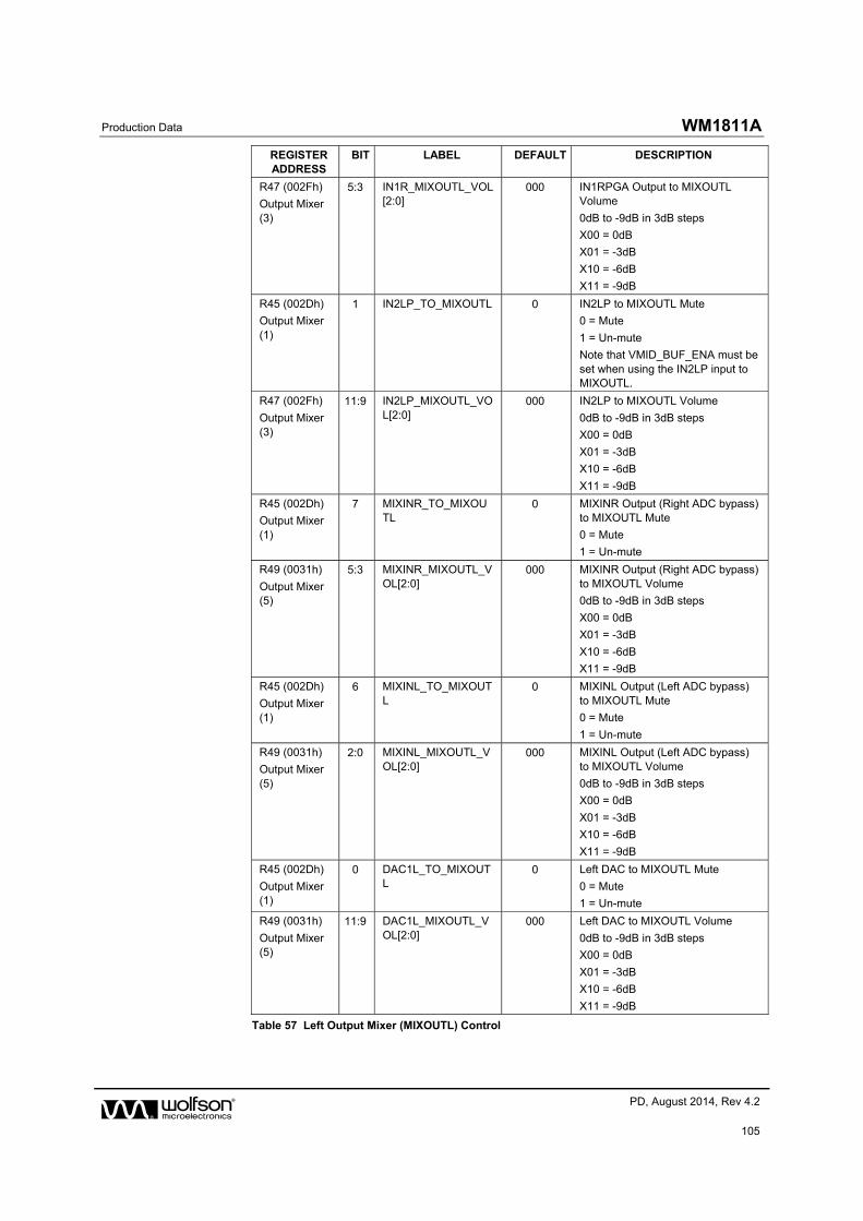
Production Data WM1811A
w PD, August 2014, Rev 4.2
105
REGISTER ADDRESS
BIT LABEL DEFAULT DESCRIPTION
R47 (002Fh)
Output Mixer (3)
5:3 IN1R_MIXOUTL_VOL[2:0]
000 IN1RPGA Output to MIXOUTL Volume
0dB to -9dB in 3dB steps
X00 = 0dB
X01 = -3dB
X10 = -6dB
X11 = -9dB
R45 (002Dh)
Output Mixer (1)
1 IN2LP_TO_MIXOUTL 0 IN2LP to MIXOUTL Mute
0 = Mute
1 = Un-mute
Note that VMID_BUF_ENA must be set when using the IN2LP input to MIXOUTL.
R47 (002Fh)
Output Mixer (3)
11:9 IN2LP_MIXOUTL_VOL[2:0]
000 IN2LP to MIXOUTL Volume
0dB to -9dB in 3dB steps
X00 = 0dB
X01 = -3dB
X10 = -6dB
X11 = -9dB
R45 (002Dh)
Output Mixer (1)
7 MIXINR_TO_MIXOUTL
0 MIXINR Output (Right ADC bypass) to MIXOUTL Mute
0 = Mute
1 = Un-mute
R49 (0031h)
Output Mixer (5)
5:3 MIXINR_MIXOUTL_VOL[2:0]
000 MIXINR Output (Right ADC bypass) to MIXOUTL Volume
0dB to -9dB in 3dB steps
X00 = 0dB
X01 = -3dB
X10 = -6dB
X11 = -9dB
R45 (002Dh)
Output Mixer (1)
6 MIXINL_TO_MIXOUTL
0 MIXINL Output (Left ADC bypass) to MIXOUTL Mute
0 = Mute
1 = Un-mute
R49 (0031h)
Output Mixer (5)
2:0 MIXINL_MIXOUTL_VOL[2:0]
000 MIXINL Output (Left ADC bypass) to MIXOUTL Volume
0dB to -9dB in 3dB steps
X00 = 0dB
X01 = -3dB
X10 = -6dB
X11 = -9dB
R45 (002Dh)
Output Mixer (1)
0 DAC1L_TO_MIXOUTL
0 Left DAC to MIXOUTL Mute
0 = Mute
1 = Un-mute
R49 (0031h)
Output Mixer (5)
11:9 DAC1L_MIXOUTL_VOL[2:0]
000 Left DAC to MIXOUTL Volume
0dB to -9dB in 3dB steps
X00 = 0dB
X01 = -3dB
X10 = -6dB
X11 = -9dB
Table 57 Left Output Mixer (MIXOUTL) Control

WM1811A Production Data
w PD, August 2014, Rev 4.2
106
REGISTER ADDRESS
BIT LABEL DEFAULT DESCRIPTION
R46 (002Eh)
Output Mixer (2)
5 IN2LN_TO_MIXOUTR
0 IN2LN to MIXOUTR Mute
0 = Mute
1 = Un-mute
Note that VMID_BUF_ENA must be set when using the IN2LN input to MIXOUTR.
R50 (0032h)
Output Mixer (6)
8:6 IN2LN_MIXOUTR_VOL[2:0]
000 IN2LN to MIXOUTR Volume
0dB to -9dB in 3dB steps
X00 = 0dB
X01 = -3dB
X10 = -6dB
X11 = -9dB
R46 (002Eh)
Output Mixer (2)
4 IN2RN_TO_MIXOUTR
0 IN2RN to MIXOUTR Mute
0 = Mute
1 = Un-mute
Note that VMID_BUF_ENA must be set when using the IN2RN input to MIXOUTR.
R48 (0030h)
Output Mixer (4)
8:6 IN2RN_MIXOUTR_VOL[2:0]
000 IN2RN to MIXOUTR Volume
0dB to -9dB in 3dB steps
X00 = 0dB
X01 = -3dB
X10 = -6dB
X11 = -9dB
R46 (002Eh)
Output Mixer (2)
3 IN1L_TO_MIXOUTR 0 IN1L PGA Output to MIXOUTR Mute
0 = Mute
1 = Un-mute
R48 (0030h)
Output Mixer (4)
5:3 IN1L_MIXOUTR_VOL[2:0]
000 IN1L PGA Output to MIXOUTR Volume
0dB to -9dB in 3dB steps
X00 = 0dB
X01 = -3dB
X10 = -6dB
X11 = -9dB
R46 (002Eh)
Output Mixer (2)
2 IN1R_TO_MIXOUTR 0 IN1R PGA Output to MIXOUTR Mute
0 = Mute
1 = Un-mute
R48 (0030h)
Output Mixer (4)
2:0 IN1R_MIXOUTR_VOL[2:0]
000 IN1R PGA Output to MIXOUTR Volume
0dB to -9dB in 3dB steps
X00 = 0dB
X01 = -3dB
X10 = -6dB
X11 = -9dB
R46 (002Eh)
Output Mixer (2)
1 IN2RP_TO_MIXOUTR
0 IN2RP to MIXOUTR Mute
0 = Mute
1 = Un-mute
Note that VMID_BUF_ENA must be set when using the IN2RP input to MIXOUTR.

Production Data WM1811A
w PD, August 2014, Rev 4.2
107
REGISTER ADDRESS
BIT LABEL DEFAULT DESCRIPTION
R48 (0030h)
Output Mixer (4)
11:9 IN2RP_MIXOUTR_VOL[2:0]
000 IN2RP to MIXOUTR Volume
0dB to -9dB in 3dB steps
X00 = 0dB
X01 = -3dB
X10 = -6dB
X11 = -9dB
R46 (002Eh)
Output Mixer (2)
7 MIXINL_TO_MIXOUTR
0 MIXINL Output (LeftADC bypass) to MIXOUTR Mute
0 = Mute
1 = Un-mute
R50 (0032h)
Output Mixer (6)
5:3 MIXINL_MIXOUTR_VOL[2:0]
000 MIXINL Output (LeftADC bypass) to MIXOUTR Volume
0dB to -9dB in 3dB steps
X00 = 0dB
X01 = -3dB
X10 = -6dB
X11 = -9dB
R46 (002Eh)
Output Mixer (2)
6 MIXINR_TO_MIXOUTR
0 MIXINR Output (RightADC bypass) to MIXOUTR Mute
0 = Mute
1 = Un-mute
R50 (0032h)
Output Mixer (6)
2:0 MIXINR_MIXOUTR_VOL[2:0]
000 MIXINR Output (RightADC bypass) to MIXOUTR Volume
0dB to -9dB in 3dB steps
X00 = 0dB
X01 = -3dB
X10 = -6dB
X11 = -9dB
R46 (002Eh)
Output Mixer (2)
0 DAC1R_TO_MIXOUTR
0 Right DAC to MIXOUTR Mute
0 = Mute
1 = Un-mute
R50 (0032h)
Output Mixer (6)
11:9 DAC1R_MIXOUTR_VOL[2:0]
000 Right DAC to MIXOUTR Volume
0dB to -9dB in 3dB steps
X00 = 0dB
X01 = -3dB
X10 = -6dB
X11 = -9dB
Table 58 Right Output Mixer (MIXOUTR) Control

WM1811A Production Data
w PD, August 2014, Rev 4.2
108
SPEAKER MIXER CONTROL
The Speaker Mixer path select and volume controls are described in Table 59 for the Left Channel (SPKMIXL) and Table 60 for the Right Channel (SPKMIXR).
Care should be taken when enabling more than one path to a speaker mixer in order to avoid clipping.The gain of each input path is adjustable using a selectable -6dB control in each path to facilitate this. Each Speaker Mixer output can also be muted using the SPKMIXL_VOL or SPKMIXR_VOL register.
Note that the DAC input levels may also be controlled by the DAC Output Paths digital volume controls (see “Digital Mixing”) and also (when applicable) by the Audio Interface Input Paths digital volume controls (see “Digital Volume and Filter Control”).
When using the IN1LP or IN1RP signal paths to the speaker mixers, the buffered VMID reference must be enabled, using the VMID_BUF_ENA register, as described in “Reference Voltages and Master Bias”.
REGISTER ADDRESS
BIT LABEL DEFAULT DESCRIPTION
R54 (0034h)
Speaker Mixer
7 MIXINL_TO_SPKMIXL 0 MIXINL (Left ADC bypass) to SPKMIXL Mute
0 = Mute
1 = Un-mute
5 IN1LP_TO_SPKMIXL 0 IN1LP to SPKMIXL Mute
0 = Mute
1 = Un-mute
Note that VMID_BUF_ENA must be set when using the IN1LP input to SPKMIXL.
3 MIXOUTL_TO_SPKMIXL
0 Left Mixer Output to SPKMIXL Mute
0 = Mute
1 = Un-mute
1 DAC1L_TO_SPKMIXL 0 Left DAC to SPKMIXL Mute
0 = Mute
1 = Un-mute
R34 (0022h)
SPKMIXL Attenuation
5 MIXINL_SPKMIXL_VOL
0 MIXINL (Left ADC bypass) to SPKMIXL Fine Volume Control
0 = 0dB
1 = -6dB
4 IN1LP_SPKMIXL_VOL 0 IN1LP to SPKMIXL Fine Volume Control
0 = 0dB
1 = -6dB
3 MIXOUTL_SPKMIXL_VOL
0 Left Mixer Output to SPKMIXL Fine Volume Control
0 = 0dB
1 = -6dB
2 DAC1L_SPKMIXL_VOL
0 Left DAC to SPKMIXL Fine Volume Control
0 = 0dB
1 = -6dB
1:0 SPKMIXL_VOL [1:0] 11 Left Speaker Mixer Volume Control
00 = 0dB
01 = Reserved
10 = Reserved
11 = Mute
Table 59 Left Speaker Mixer (SPKMIXL) Control

Production Data WM1811A
w PD, August 2014, Rev 4.2
109
REGISTER ADDRESS
BIT LABEL DEFAULT DESCRIPTION
R54 (0034h)
Speaker Mixer
6 MIXINR_TO_SPKMIXR 0 MIXINR (Right ADC bypass) to SPKMIXR Mute
0 = Mute
1 = Un-mute
4 IN1RP_TO_SPKMIXR 0 IN1RP to SPKMIXR Mute
0 = Mute
1 = Un-mute
Note that VMID_BUF_ENA must be set when using the IN1RP input to SPKMIXR.
2 MIXOUTR_TO_SPKMIXR
0 Right Mixer Output to SPKMIXR Mute
0 = Mute
1 = Un-mute
0 DAC1R_TO_SPKMIXR 0 Right DAC to SPKMIXR Mute
0 = Mute
1 = Un-mute
R35 (0023h)
SPKMIXR Attenuation
5 MIXINR_SPKMIXR_VOL
0 MIXINR (Right ADC bypass) to SPKMIXR Fine Volume Control
0 = 0dB
1 = -6dB
4 IN1RP_SPKMIXR_VOL
0 IN1RP to SPKMIXR Fine Volume Control
0 = 0dB
1 = -6dB
3 MIXOUTR_SPKMIXR_VOL
0 Right Mixer Output to SPKMIXR Fine Volume Control
0 = 0dB
1 = -6dB
2 DAC1R_SPKMIXR_VOL
0 Right DAC to SPKMIXR Fine Volume Control
0 = 0dB
1 = -6dB
1:0 SPKMIXR_VOL [1:0] 11 Right Speaker Mixer Volume Control
00 = 0dB
01 = Reserved
10 = Reserved
11 = Mute
Table 60 Right Speaker Mixer (SPKMIXR) Control

WM1811A Production Data
w PD, August 2014, Rev 4.2
110
OUTPUT SIGNAL PATH VOLUME CONTROL
There are six output PGAs - MIXOUTLVOL, MIXOUTRVOL, HPOUT1LVOL, HPOUT1RVOL, SPKLVOL and SPKRVOL. Each can be independently controlled, with MIXOUTLVOL and MIXOUTRVOL providing volume control to both the earpiece and line drivers, HPOUT1LVOL and HPOUT1RVOL to the headphone driver, and SPKLVOL and SPKRVOL to the speaker drivers.
The volume control of each of these output PGAs can be adjusted over a wide range of values. To minimise pop noise, it is recommended that only the MIXOUTLVOL, MIXOUTRVOL, HPOUT1LVOL, HPOUT1RVOL, SPKLVOL and SPKRVOL are modified while the output signal path is active. Other gain controls are provided in the signal paths to provide scaling of signals from different sources, and to prevent clipping when multiple signals are mixed. However, to prevent pop noise, it is recommended that those other gain controls should not be modified while the signal path is active.
To prevent "zipper noise", a zero-cross function is provided on theoutput PGAs. When this feature is enabled, volume updates will not take place until a zero-crossing is detected. In the case of a long period without zero-crossings, a timeout function is provided. When the zero-cross function is enabled, the volume will update after the timeout period if no earlier zero-cross has occurred. The timeout clock is enabled using TOCLK_ENA; the timeout period is set by TOCLK_DIV. See “Clocking and Sample Rates” for more information on these fields.
The mixer output PGA controls are shown in Table 61.The MIXOUT_VU bits control the loading of the output mixer PGA volume data. When MIXOUT_VU is set to 0, the volume control data will be loaded into the respective control register, but will not actually change the gain setting. The output mixer PGA volume settings are both updated when a 1 is written toeither MIXOUT_VU bit. This makes it possible to update the gain of both output paths simultaneously.
REGISTER ADDRESS
BIT LABEL DEFAULT DESCRIPTION
R32 (0020h)
Left OPGA Volume
8 MIXOUT_VU N/A Mixer Output PGA Volume Update
Writing a 1 to this bit will update MIXOUTLVOL and MIXOUTRVOL volumes simultaneously.
7 MIXOUTL_ZC 0 MIXOUTLVOL (Left Mixer Output PGA) Zero Cross Enable
0 = Zero cross disabled
1 = Zero cross enabled
6 MIXOUTL_MUTE_N 1 MIXOUTLVOL (Left Mixer Output PGA) Mute
0 = Mute
1 = Un-mute
5:0 MIXOUTL_VOL[5:0] 39h
(0dB)
MIXOUTLVOL(Left Mixer Output PGA) Volume
-57dB to +6dB in 1dB steps
00_0000 = -57dB
00_0001 = -56dB
… (1dB steps)
11_1111 = +6dB
(See Table 64 for output PGA volume control range)
R33 (0021h)
Right OPGA Volume
8 MIXOUT_VU N/A Mixer Output PGA Volume Update
Writing a 1 to this bit will update MIXOUTLVOL and MIXOUTRVOL volumes simultaneously.
7 MIXOUTR_ZC 0 MIXOUTRVOL (Right Mixer Output PGA) Zero Cross Enable
0 = Zero cross disabled
1 = Zero cross enabled
6 MIXOUTR_MUTE_N 1 MIXOUTLVOL (Right Mixer Output PGA) Mute
0 = Mute
1 = Un-mute

Production Data WM1811A
w PD, August 2014, Rev 4.2
111
REGISTER ADDRESS
BIT LABEL DEFAULT DESCRIPTION
5:0 MIXOUTR_VOL[5:0] 39h
(0dB)
MIXOUTRVOL (Right Mixer Output PGA) Volume
-57dB to +6dB in 1dB steps
00_0000 = -57dB
00_0001 = -56dB
… (1dB steps)
11_1111 = +6dB
(See Table 64 for output PGA volume control range)
Table 61 Mixer Output PGA (MIXOUTLVOL, MIXOUTRVOL) Control
The headphone output PGA controls are shown inTable 62.The HPOUT1_VU bits control the loading of the headphone PGA volume data. When HPOUT1_VU is set to 0, the volume control data will be loaded into the respective control register, but will not actually change the gain setting. The headphone PGA volume settings are both updated when a 1 is written toeither HPOUT1_VU bit. This makes it possible to update the gain of both output paths simultaneously.
The HPOUT1_ATTN register controls a -3dB attenuation function in the HPOUT1L and HPOUT1R signal paths. (Note that this single register applies to the Left and Right output paths.) The output path Signal to Noise Ratio (SNR) may be improved when the HPOUT1_ATTN bit is set, but the maximum signal level is reduced by 3dB.
Note that, when the HPOUT1_ATTN register is updated in Register Control mode (CP_DYN_PWR=0), the HPOUT1_ATTN function is not fully implemented until a ‘1’ has been written to HPOUT1_VU. See “Charge Pump” for details of the CP_DYN_PWR register bit.
The DAC1L_TO_HPOUT1L and DAC1R_TO_HPOUT1R register bits allow the DACL and DACR outputs to be selected as the single input to the HPOUT1L and HPOUT1R headphone output PGAs respectively. When these bits are asserted, the respective output mixer settings are ignored, and only the DAC path(s) are enabled. Note that these register controls are provided for software compatibility with WM8994; it is not recommended to use these register bits.
REGISTER ADDRESS
BIT LABEL DEFAULT DESCRIPTION
R28 (001Ch)
Left Output Volume
8 HPOUT1_VU N/A Headphone Output PGA Volume Update
Writing a 1 to this bit will update HPOUT1LVOL and HPOUT1RVOL volumes simultaneously.
7 HPOUT1L_ZC 0 HPOUT1LVOL (Left Headphone Output PGA) Zero Cross Enable
0 = Zero cross disabled
1 = Zero cross enabled
6 HPOUT1L_MUTE_N
1 HPOUT1LVOL (Left Headphone Output PGA) Mute
0 = Mute
1 = Un-mute
5:0 HPOUT1L_VOL[5:0]
2Dh
(-12dB)
HPOUT1LVOL (Left Headphone Output PGA) Volume
-57dB to +6dB in 1dB steps
00_0000 = -57dB
00_0001 = -56dB
… (1dB steps)
11_1111 = +6dB
(See Table 64 for output PGA volume control range)
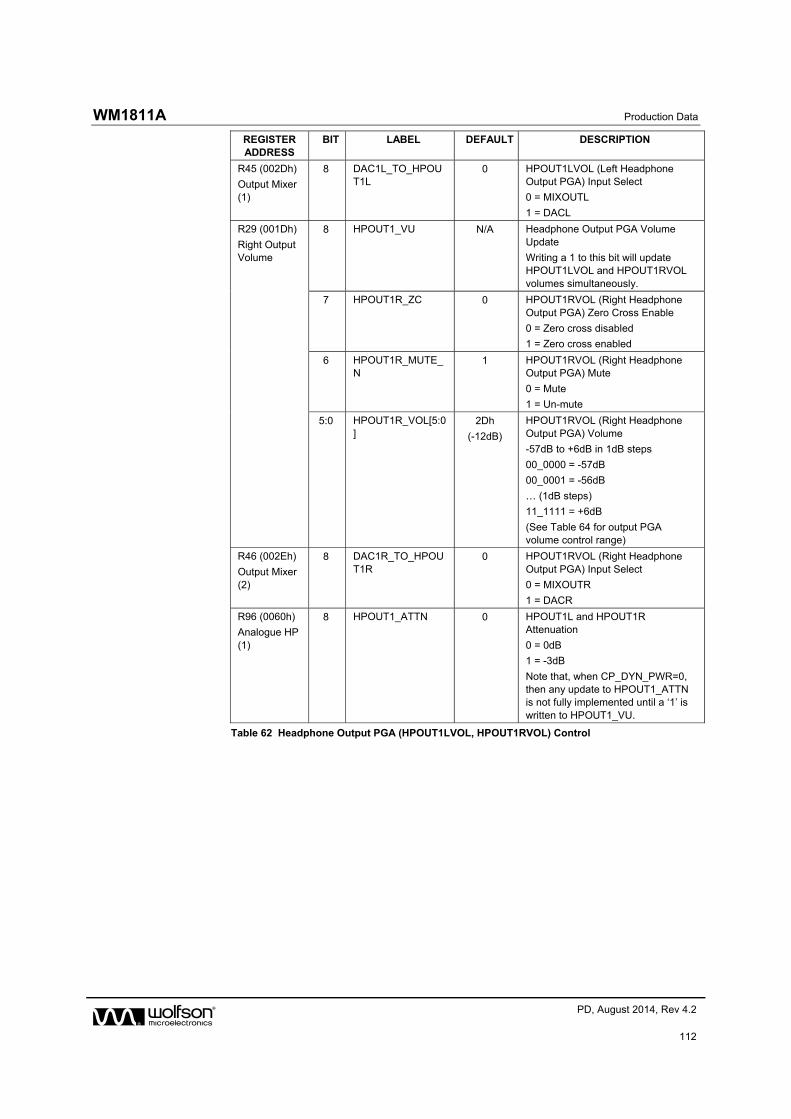
WM1811A Production Data
w PD, August 2014, Rev 4.2
112
REGISTER ADDRESS
BIT LABEL DEFAULT DESCRIPTION
R45 (002Dh)
Output Mixer (1)
8 DAC1L_TO_HPOUT1L
0 HPOUT1LVOL (Left Headphone Output PGA) Input Select
0 = MIXOUTL
1 = DACL
R29 (001Dh)
Right Output Volume
8 HPOUT1_VU N/A Headphone Output PGA Volume Update
Writing a 1 to this bit will update HPOUT1LVOL and HPOUT1RVOL volumes simultaneously.
7 HPOUT1R_ZC 0 HPOUT1RVOL (Right Headphone Output PGA) Zero Cross Enable
0 = Zero cross disabled
1 = Zero cross enabled
6 HPOUT1R_MUTE_N
1 HPOUT1RVOL (Right Headphone Output PGA) Mute
0 = Mute
1 = Un-mute
5:0 HPOUT1R_VOL[5:0]
2Dh
(-12dB)
HPOUT1RVOL (Right Headphone Output PGA) Volume
-57dB to +6dB in 1dB steps
00_0000 = -57dB
00_0001 = -56dB
… (1dB steps)
11_1111 = +6dB
(See Table 64 for output PGA volume control range)
R46 (002Eh)
Output Mixer (2)
8 DAC1R_TO_HPOUT1R
0 HPOUT1RVOL (Right Headphone Output PGA) Input Select
0 = MIXOUTR
1 = DACR
R96 (0060h)
Analogue HP (1)
8 HPOUT1_ATTN 0 HPOUT1L and HPOUT1R Attenuation
0 = 0dB
1 = -3dB
Note that, when CP_DYN_PWR=0, then any update to HPOUT1_ATTN is not fully implemented until a ‘1’ is written to HPOUT1_VU.
Table 62 Headphone Output PGA (HPOUT1LVOL, HPOUT1RVOL) Control

Production Data WM1811A
w PD, August 2014, Rev 4.2
113
The speakeroutput PGA controls are shown in Table 63.The SPKOUT_VU bits control the loading of the speaker PGA volume data. When SPKOUT_VU is set to 0, the volume control data will be loaded into the respective control register, but will not actually change the gain setting. The speaker PGA volume settings are both updated when a 1 is written toeither SPKOUT_VU bit. This makes it possible to update the gain of both output paths simultaneously.
REGISTER ADDRESS
BIT LABEL DEFAULT DESCRIPTION
R38 (0026h)
Speaker Volume Left
8 SPKOUT_VU N/A SpeakerOutput PGA Volume Update
Writing a 1 to this bit will update SPKLVOL and SPKRVOL volumes simultaneously.
7 SPKOUTL_ZC 0 SPKLVOL (Left Speaker Output PGA) Zero Cross Enable
0 = Zero cross disabled
1 = Zero cross enabled
6 SPKOUTL_MUTE_N 1 SPKLVOL (Left Speaker Output PGA) Mute
0 = Mute
1 = Un-mute
5:0 SPKOUTL_VOL[5:0] 39h
(0dB)
SPKLVOL (Left Speaker Output PGA) Volume
-57dB to +6dB in 1dB steps
00_0000 = -57dB
00_0001 = -56dB
… (1dB steps)
11_1111 = +6dB
(See Table 64 for output PGA volume control range)
R39 (0027h)
Speaker Volume Right
8 SPKOUT_VU N/A Speaker PGA Volume Update
Writing a 1 to this bit will update SPKLVOL and SPKRVOL volumes simultaneously.
7 SPKOUTR_ZC 0 SPKRVOL (Right Speaker Output PGA) Zero Cross Enable
0 = Zero cross disabled
1 = Zero cross enabled
6 SPKOUTR_MUTE_N
1 SPKRVOL (Right Speaker Output PGA) Mute
0 = Mute
1 = Un-mute
5:0 SPKOUTR_VOL[5:0] 39h
(0dB)
SPKRVOL (Right Speaker Output PGA) Volume
-57dB to +6dB in 1dB steps
00_0000 = -57dB
00_0001 = -56dB
… (1dB steps)
11_1111 = +6dB
(See Table 64 for output PGA volume control range)
Table 63 Speaker Output PGA (SPKLVOL, SPKRVOL) Control

WM1811A Production Data
w PD, August 2014, Rev 4.2
114
PGA GAIN SETTING VOLUME (dB) PGA GAIN SETTING VOLUME (dB)
00h -57 20h -25
01h -56 21h -24
02h -55 22h -23
03h -54 23h -22
04h -53 24h -21
05h -52 25h -20
06h -51 26h -19
07h -50 27h -18
08h -49 28h -17
09h -48 29h -16
0Ah -47 2Ah -15
0Bh -46 2Bh -14
0Ch -45 2Ch -13
0Dh -44 2Dh -12
0Eh -43 2Eh -11
0Fh -42 2Fh -10
10h -41 30h -9
11h -40 31h -8
12h -39 32h -7
13h -38 33h -6
14h -37 34h -5
15h -36 35h -4
16h -35 36h -3
17h -34 37h -2
18h -33 38h -1
19h -32 39h 0
1Ah -31 3Ah +1
1Bh -30 3Bh +2
1Ch -29 3Ch +3
1Dh -28 3Dh +4
1Eh -27 3Eh +5
1Fh -26 3Fh +6
Table 64 Output PGA Volume Range

Production Data WM1811A
w PD, August 2014, Rev 4.2
115
SPEAKER BOOST MIXER
Each speaker driver has its own boost mixer which performs a dual role. It allows the output from the left speaker mixer (via SPKLVOL) or the right speaker mixer (via SPKRVOL) to be routed to either speaker driver. The speaker boost mixers are controlled using the registers defined in Table 65 below.
The second function of the speaker boost mixers is that they provide an additional AC gain (boost) function to shift signal levels between the AVDD1 and SPKVDD voltage domains for maximum output power. The AC gain (boost) function is described in the “Analogue Outputs” section.
REGISTER ADDRESS
BIT LABEL DEFAULT DESCRIPTION
R36 (0024h)
SPKOUT Mixers
4 SPKMIXL_TO_SPKOUTL
1 SPKMIXL Left Speaker Mixer to Left Speaker Mute
0 = Mute
1 = Un-mute
3 SPKMIXR_TO_SPKOUTL
0 SPKMIXR Right Speaker Mixer to Left Speaker Mute
0 = Mute
1 = Un-mute
1 SPKMIXL_TO_SPKOUTR
0 SPKMIXL Left Speaker Mixer to Right Speaker Mute
0 = Mute
1 = Un-mute
0 SPKMIXR_TO_SPKOUTR
1 SPKMIXR Right Speaker Mixer to Right Speaker Mute
0 = Mute
1 = Un-mute
Table 65 Speaker Boost Mixer (SPKOUTLBOOST, SPKOUTRBOOST) Control
EARPIECE DRIVER MIXER
The earpiece driver has a dedicated mixer, HPOUT2MIX, which is controlled using the registers defined in Table 66. The earpiece driver is configurable to select output from the left output mixer (via MIXOUTLVOL) or the right output mixer (via MIXOUTRVOL).
Care should be taken to avoid clipping when enabling more than one path to the earpiece driver. The HPOUT2VOL volume control can be used to avoid clipping when more than one full scale signal is input to the mixer.

WM1811A Production Data
w PD, August 2014, Rev 4.2
116
REGISTER ADDRESS
BIT LABEL DEFAULT DESCRIPTION
R31 (001Fh)
HPOUT2 Volume
5 HPOUT2_MUTE 1 HPOUT2 (Earpiece Driver) Mute
0 = Un-mute
1 = Mute
4 HPOUT2_VOL 0 HPOUT2 (Earpiece Driver) Volume
0 = 0dB
1 = -6dB
R51 (0033h)
HPOUT2 Mixer
4 MIXOUTLVOL_TO_HPOUT2
0 MIXOUTLVOL (Left Output Mixer PGA) to Earpiece Driver
0 = Mute
1 = Un-mute
3 MIXOUTRVOL_TO_HPOUT2
0 MIXOUTRVOL (Right Output Mixer PGA) to Earpiece Driver
0 = Mute
1 = Un-mute
Table 66 Earpiece Driver Mixer (HPOUT2MIX) Control
LINE OUTPUT MIXERS
The WM1811A provides two pairsof line outputs, both with highly configurable output mixers. The outputs LINEOUT1N and LINEOUT1P can be configured as two single-ended outputs or as a differential output. In the same manner, LINEOUT2N and LINEOUT2P can be configured either as two single-ended outputs or as a differential output. The respective line output mixers can be configured in single-ended mode or differential mode; each mode supports multiple signal path configurations.
LINEOUT1 single-ended mode is selected by setting LINEOUT1_MODE = 1. In single-ended mode, any of three possible signal paths may be enabled:
MIXOUTL (left output mixer) to LINEOUT1P
MIXOUTR (right output mixer) to LINEOUT1N
MIXOUTL (left output mixer) to LINEOUT1N
LINEOUT1 differential mode is selected by setting LINEOUT1_MODE = 0. In differential mode, any of three possible signal paths may be enabled:
MIXOUTL (left output mixer) to LINEOUT1N and LINEOUT1P
IN1L (input PGA) to LINEOUT1Nand LINEOUT1P
IN1R (input PGA) to LINEOUT1Nand LINEOUT1P
The LINEOUT1output mixers are controlled as described in Table 67. Care should be taken to avoid clipping when enabling more than one path to the line outputmixers. The LINEOUT1_VOL control can be used to provide -6dB attenuation when more than one full scale signal is applied.
When using the LINEOUT1 mixers in single-ended mode, a buffered VMID must be enabled. This is achieved by setting LINEOUT_VMID_BUF_ENA, as described in the “Analogue Outputs” section.
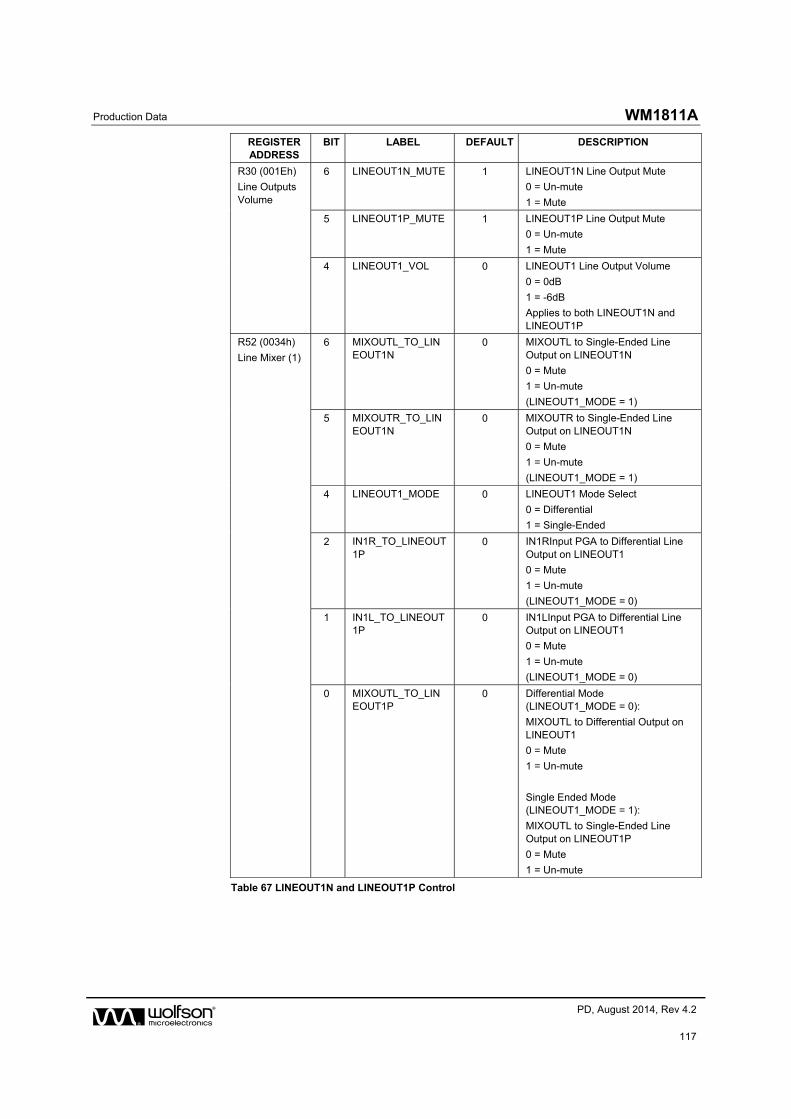
Production Data WM1811A
w PD, August 2014, Rev 4.2
117
REGISTER ADDRESS
BIT LABEL DEFAULT DESCRIPTION
R30 (001Eh)
Line Outputs Volume
6 LINEOUT1N_MUTE 1 LINEOUT1N Line Output Mute
0 = Un-mute
1 = Mute
5 LINEOUT1P_MUTE 1 LINEOUT1P Line Output Mute
0 = Un-mute
1 = Mute
4 LINEOUT1_VOL 0 LINEOUT1 Line Output Volume
0 = 0dB
1 = -6dB
Applies to both LINEOUT1N and LINEOUT1P
R52 (0034h)
Line Mixer (1)
6 MIXOUTL_TO_LINEOUT1N
0 MIXOUTL to Single-Ended Line Output on LINEOUT1N
0 = Mute
1 = Un-mute
(LINEOUT1_MODE = 1)
5 MIXOUTR_TO_LINEOUT1N
0 MIXOUTR to Single-Ended Line Output on LINEOUT1N
0 = Mute
1 = Un-mute
(LINEOUT1_MODE = 1)
4 LINEOUT1_MODE 0 LINEOUT1 Mode Select
0 = Differential
1 = Single-Ended
2 IN1R_TO_LINEOUT1P
0 IN1RInput PGA to Differential Line Output on LINEOUT1
0 = Mute
1 = Un-mute
(LINEOUT1_MODE = 0)
1 IN1L_TO_LINEOUT1P
0 IN1LInput PGA to Differential Line Output on LINEOUT1
0 = Mute
1 = Un-mute
(LINEOUT1_MODE = 0)
0 MIXOUTL_TO_LINEOUT1P
0 Differential Mode (LINEOUT1_MODE = 0):
MIXOUTL to Differential Output on LINEOUT1
0 = Mute
1 = Un-mute
Single Ended Mode (LINEOUT1_MODE = 1):
MIXOUTL to Single-Ended Line Output on LINEOUT1P
0 = Mute
1 = Un-mute
Table 67 LINEOUT1N and LINEOUT1P Control
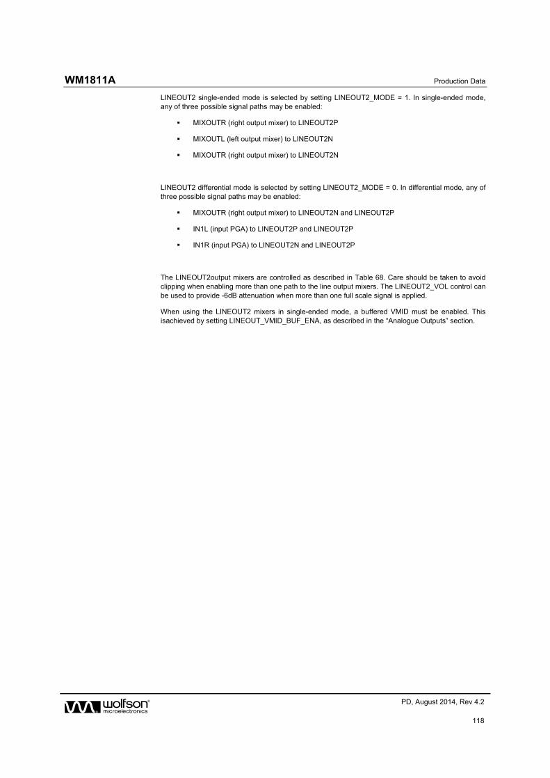
WM1811A Production Data
w PD, August 2014, Rev 4.2
118
LINEOUT2 single-ended mode is selected by setting LINEOUT2_MODE = 1. In single-ended mode, any of three possible signal paths may be enabled:
MIXOUTR (right output mixer) to LINEOUT2P
MIXOUTL (left output mixer) to LINEOUT2N
MIXOUTR (right output mixer) to LINEOUT2N
LINEOUT2 differential mode is selected by setting LINEOUT2_MODE = 0. In differential mode, any of three possible signal paths may be enabled:
MIXOUTR (right output mixer) to LINEOUT2N and LINEOUT2P
IN1L (input PGA) to LINEOUT2P and LINEOUT2P
IN1R (input PGA) to LINEOUT2N and LINEOUT2P
The LINEOUT2output mixers are controlled as described in Table 68. Care should be taken to avoid clipping when enabling more than one path to the line output mixers. The LINEOUT2_VOL control can be used to provide -6dB attenuation when more than one full scale signal is applied.
When using the LINEOUT2 mixers in single-ended mode, a buffered VMID must be enabled. This isachieved by setting LINEOUT_VMID_BUF_ENA, as described in the “Analogue Outputs” section.

Production Data WM1811A
w PD, August 2014, Rev 4.2
119
REGISTER ADDRESS
BIT LABEL DEFAULT DESCRIPTION
R30 (001Eh)
Line Outputs Volume
2 LINEOUT2N_MUTE 1 LINEOUT2N Line Output Mute
0 = Un-mute
1 = Mute
1 LINEOUT2P_MUTE 1 LINEOUT2P Line Output Mute
0 = Un-mute
1 = Mute
0 LINEOUT2_VOL 0 LINEOUT2 Line Output Volume
0 = 0dB
1 = -6dB
Applies to both LINEOUT2N and LINEOUT2P
R53 (0035h)
Line Mixer (2)
6 MIXOUTR_TO_LINEOUT2N
0 MIXOUTR to Single-Ended Line Output on LINEOUT2N
0 = Mute
1 = Un-mute
(LINEOUT2_MODE = 1)
5 MIXOUTL_TO_LINEOUT2N
0 MIXOUTL to Single-Ended Line Output on LINEOUT2N
0 = Mute
1 = Un-mute
(LINEOUT2_MODE = 1)
4 LINEOUT2_MODE 0 LINEOUT2 Mode Select
0 = Differential
1 = Single-Ended
2 IN1L_TO_LINEOUT2P
0 IN1L Input PGA to Differential Line Output on LINEOUT2
0 = Mute
1 = Un-mute
(LINEOUT2_MODE = 0)
1 IN1R_TO_LINEOUT2P
0 IN1R Input PGA to Differential Line Output on LINEOUT2
0 = Mute
1 = Un-mute
(LINEOUT2_MODE = 0)
0 MIXOUTR_TO_LINEOUT2P
0 Differential Mode (LINEOUT2_MODE = 0):
MIXOUTR to Differential Output on LINEOUT2
0 = Mute
1 = Un-mute
Single-Ended Mode (LINEOUT2_MODE = 0):
MIXOUTR to Single-Ended Line Output on LINEOUT2P
0 = Mute
1 = Un-mute
Table 68 LINEOUT2N and LINEOUT2P Control

WM1811A Production Data
w PD, August 2014, Rev 4.2
120
CHARGE PUMP
The WM1811A incorporates a dual-mode Charge Pump which generates the supply rails for the headphone output drivers, HPOUT1L and HPOUT1R.
The Charge Pump has a single supply input, CPVDD, and generates split rails CPVOUTP and CPVOUTN according to the selected mode of operation.
The Charge Pump connections are illustrated in Figure 28 (see “Applications Information” for external component values). An input decoupling capacitor may also be required at CPVDD, depending upon the system configuration.
Figure 28 Charge Pump External Connections
The Charge Pump is enabled by setting the CP_ENA bit. When enabled, the charge pump adjusts the output voltages (CPVOUTP and CPVOUTN) as well as the switching frequency in order to optimise the power consumption according to the operating conditions. This can take two forms, which are selected using the CP_DYN_PWR register bit.
Register control (CP_DYN_PWR = 0)
Dynamic control (CP_DYN_PWR = 1)
Under Register control, the HPOUT1L_VOL and HPOUT1R_VOL register settings are used to control the charge pump mode of operation.
Under Dynamic control, the audio signal level in the digital audio interface is used to control the charge pump mode of operation. The CP_DYN_SRC_SEL register determines which of the digital signal paths is used for this function - this may be the AIF1 DAC path or the AIF2 DAC path. The CP_DYN_SRC_SEL should be set according to the active source for the HPOUT1L and HPOUT1R outputs.
The Dynamic Charge Pump Control mode is the Wolfson ‘Class W’ mode, which allows the power consumption to be optimised in real time, but can only be used if a single AIF source is the only signal source. The Class W mode should not be used if any of the bypass paths are used to feed analogue inputs into the output signal path, or if more than one AIF source is used to feed the headphone output via the Digital Mixers.
The Charge Pump operating mode defaults to Register control; Dynamic control may be selected by setting the CP_DYN_PWR register bit, if appropriate.
Note that the charge pump clock is derived from internal clock SYSCLK; either MCLK or the FLL output selectable using the SYSCLK_SRC bit. Under normal circumstances an external clock signal must be present for the charge pump to function. However, the FLL has a free-running mode that does not require an external clock but will generate an internal clock suitable for running the charge pump. The clock division from SYSCLK is handled transparently by the WM1811A without user intervention, as long as SYSCLK and sample rates are set correctly. Refer to the “Clocking and Sample Rates” section for more detail on the FLL and clocking configuration.

Production Data WM1811A
w PD, August 2014, Rev 4.2
121
When the Charge Pump is disabled, the output can be left floating or can be actively discharged, depending on the CP_DISCH control bit.
If the headphone output drivers (HPOUT1L and HPOUT1R) are not used, then the Charge Pump and the associated external components are not required. The Charge Pump and Headphone drivers should not be enabled in this case (CP_ENA=0, HPOUT1L_ENA=0, HPOUT1R_ENA=0).
If the Charge Pump is not used, and the associated external components are omitted, then the CPCA and CPCB pins can be left floating; the CPVOUTP and CPVOUTN pins should be grounded as illustrated in Figure 29.
Note that, when the Charge Pump is disabled, it is still recommended that the CPVDD pin is kept within its recommended operating conditions.
Figure 29 External Configuration when Charge Pump not used
The Charge Pump control fields are described in Table 69.
REGISTER ADDRESS
BIT LABEL DEFAULT DESCRIPTION
R76 (004Ch)
Charge Pump (1)
15 CP_ENA 0 Enable charge-pump digits
0 = Disable
1 = Enable
R77 (004Dh)
Charge Pump (2)
15 CP_DISCH 1 Charge Pump Discharge Select
0 = Charge Pump outputs floating when disabled
1 = Charge Pump outputs discharged when disabled
R81 (0051h)
Class W (1)
9:8 CP_DYN_SRC_SEL 00 Selects the digital audio source for envelope tracking
00 = AIF1, DAC data
01 = Reserved
10 = AIF2, DAC data
11 = Reserved
0 CP_DYN_PWR 0 Enable dynamic charge pump power control
0 = charge pump controlled by volume register settings (Class G)
1 = charge pump controlled by real-time audio level (Class W)
Table 69 Charge Pump Control

WM1811A Production Data
w PD, August 2014, Rev 4.2
122
DC SERVO
The WM1811A provides a DC servo circuit on the headphone outputs HPOUT1L and HPOUT1R in order to remove DC offset from these ground-referenced outputs. When enabled, the DC servo ensures that the DC level of these outputs remains within 1mV of ground. Removal of the DC offset is important because any deviation from GND at the output pin will cause current to flow through the load under quiescent conditions, resulting in increased power consumption. Additionally, the presence of DC offsets can result in audible pops and clicks at power up and power down.
DC SERVO ENABLE AND START-UP
The DC Servo circuit is enabled on HPOUT1L and HPOUT1R by setting DCS_ENA_CHAN_0and DCS_ENA_CHAN_1respectively. When the DC Servo is enabled, the DC offset correction can be commanded in two different ways, as described below.
The DCS_TIMER_PERIOD_01 register must be set to 0000 for correct operation of the DC Servo. This register must be set to 0000 before enabling the DC Servo.
Writing a logic 1 to DCS_TRIG_STARTUP_n initiates a series of DC offset measurements and applies the necessary correction to the associated output; (‘n’ = 0for Left channel, 1for Right channel). On completion, the headphone output will be within 1mV of AGND. This mode is recommended for typical applications. Completion of the DC offset correction triggered in this way is indicated by the DCS_STARTUP_COMPLETE field, as described in Table 70. Typically, this operation takes 86ms per channel.
For correct operation of the DC Servo Start-Up mode, it is important that there is no active audio signal present on the signal path while the mode is running. The DC Servo Start-Up mode should be scheduled at the correct position within the Headphone Output Enable sequence, as described in the Analogue Output Signal Path” section. All other stages of the analogue signal path should be fully enabled prior to commanding the Start-Up mode; the DAC Digital Mute function should be used, where appropriate, to ensure there is no active audio signal present during the DC Servo measurements.
Writing a logic 1 to DCS_TRIG_DAC_WR_n causes the DC offset correction to be set to the value contained in the DCS_DAC_WR_VAL_n fields in Register R89. This mode is useful if the required offset correction has already been determined and stored; it is faster than the DCS_TRIG_STARTUP_n mode, but relies on the accuracy of the stored settings. Completion of the DC offset correction triggered in this way is indicated by the DCS_DAC_WR_COMPLETE field, as described in Table 70. Typically, this operation takes 2ms per channel.
For pop-free operation of the DC Servo DAC Write mode, it is important that the mode is scheduled at the correct position within the Headphone Output Enable sequence, as described in the “Analogue Output Signal Path” section.
The current DC offset value for each Headphone output channel can be read from the DCS_DAC_WR_VAL_nfields. These values may form the basis of settings that are subsequently used by the DC Servo in DAC Write mode. Note that these fields have a different definition for Read and Write, as described in Table 70.
When using either of the DC Servo options above, the status of the DC offset correction process is indicated by the DCS_CAL_COMPLETE field; this is the logical OR of the DCS_STARTUP_COMPLETE and DCS_DAC_WR_COMPLETE fields.
The DCS_DAC_WR_COMPLETE bits can be used as inputs to the Interrupt control circuit or used to generate an external logic signal on a GPIO pin. See “Interrupts” and “General Purpose Input/Output” for further details.
The DC Servo control fields associated with start-up operation are described in Table 70. It is important to note that, to minimise audible pops/clicks, the Start-Up and DAC Write modes of DC Servo operation should be commanded as part of a control sequence which includes muting and shorting of the headphone outputs.

Production Data WM1811A
w PD, August 2014, Rev 4.2
123
REGISTER ADDRESS
BIT LABEL DEFAULT DESCRIPTION
R84 (0054h)
DC Servo (1)
5 DCS_TRIG_STARTUP_1
0 Writing 1 to this bit selects Start-Up DC Servo mode for HPOUT1R.
In readback, a value of 1 indicates that the DC Servo Start-Up correction is in progress.
4 DCS_TRIG_STARTUP_0
0 Writing 1 to this bit selects Start-Up DC Servo mode for HPOUT1L.
In readback, a value of 1 indicates that the DC Servo Start-Up correction is in progress.
3 DCS_TRIG_DAC_WR_1
0 Writing 1 to this bit selects DAC Write DC Servo mode for HPOUT1R.
In readback, a value of 1 indicates that the DC Servo DAC Write correction is in progress.
2 DCS_TRIG_DAC_WR_0
0 Writing 1 to this bit selects DAC Write DC Servo mode for HPOUT1L.
In readback, a value of 1 indicates that the DC Servo DAC Write correction is in progress.
1 DCS_ENA_CHAN_1 0 DC Servo enable for HPOUT1R
0 = Disabled
1 = Enabled
0 DCS_ENA_CHAN_0 0 DC Servo enable for HPOUT1L
0 = Disabled
1 = Enabled
R85 (0055h)
DC Servo (2)
3:0 DCS_TIMER_PERIOD_01 [3:0]
1010 This register must be set to 0000 for correct operation of the DC Servo.
0000 = DC Servo enabled
All other values are Reserved
R88 (0058h)
DC Servo Readback
9:8 DCS_CAL_COMPLETE [1:0]
00 DC Servo Complete status
0 = DAC Write or Start-Up DC Servo mode not completed.
1 = DAC Write or Start-Up DC Servo mode complete.
Bit [1] = HPOUT1R
Bit [0] = HPOUT1L
5:4 DCS_DAC_WR_COMPLETE [1:0]
00 DC Servo DAC Write status
0 = DAC Write DC Servo mode not completed.
1 = DAC Write DC Servo mode complete.
Bit [1] = HPOUT1R
Bit [0] = HPOUT1L

WM1811A Production Data
w PD, August 2014, Rev 4.2
124
REGISTER ADDRESS
BIT LABEL DEFAULT DESCRIPTION
1:0 DCS_STARTUP_COMPLETE [1:0]
00 DC Servo Start-Up status
0 = Start-Up DC Servo mode not completed.
1 = Start-Up DC Servo mode complete.
Bit [1] = HPOUT1R
Bit [0] = HPOUT1L
R89 (0059h)
DC Servo (4)
15:8 DCS_DAC_WR_VAL_1 [7:0]
00h Writing to this field sets the DC Offset value for HPOUT1R in DAC Write DC Servo mode.
Reading this field gives the current DC Offset value for HPOUT1R.
Two’s complement format. LSB is 0.25mV. Range is -32mV to +31.75mV
7:0 DCS_DAC_WR_VAL_0 [7:0]
00h Writing to this field sets the DC Offset value for HPOUT1L in DAC Write DC Servo mode.
Reading this field gives the current DC Offset value for HPOUT1L.
Two’s complement format. LSB is 0.25mV. Range is -32mV to +31.75mV
Table 70 DC Servo Control
GPIO / INTERRUPT OUTPUTS FROM DC SERVO
When using the DC Servo Start-Up or DAC Write modes, the DCS_CAL_COMPLETE register provides readback of the status of the DC offset correction. This can be read from register R88 as described in Table 70.
The DCS_CAL_COMPLETE bits can also be used as inputs to the Interrupt control circuit and used to trigger an Interrupt event - see “Interrupts”.
The DCS_CAL_COMPLETE bits can also be used as inputs to the GPIO function and used to generate external logic signals indicating the DC Servo status. See “General Purpose Input/Output” for details of how to configure a GPIO pin to output the DC Servo status.

Production Data WM1811A
w PD, August 2014, Rev 4.2
125
ANALOGUE OUTPUTS
The speaker, headphone, earpiece and line outputs are highly configurable and may be used in many different ways.
SPEAKER OUTPUT CONFIGURATIONS
The speaker outputs SPKOUTL and SPKOUTR can be driven by either of the speaker mixers, SPKMIXL or SPKMIXR. Fine volume control is available on the speaker mixer paths using the SPKLVOL and SPKRVOL PGAs. A boost function is available on the speaker output paths. For information on the speaker mixing options, refer to the “Analogue Output Signal Path” section.
The speaker outputs SPKOUTL and SPKOUTR operate in a BTL configuration.
The speaker outputs can be configured as a pair of stereo outputs, or as a single mono output. Note that, for applications requiring only a single speaker output, it is possible to improve the THD performance by configuring the speaker outputs in mono mode.See “Typical Performance” for further details.
The mono configuration is selected by applying a logic high input to the SPKMODE pin (D5), as described in Table 71. For Stereo mode this pin should be connected to GND. Note that SPKMODE is referenced to DBVDD1.
An internal pull-up resistor is enabled by default on the SPKMODE pin; this can be configured using the SPKMODE_PU register bit described in Table 72.
SPEAKER CONFIGURATION SPKMODE PIN (D5)
Stereo Mode GND
Mono Mode DBVDD1
Table 71 SPKMODE Pin Function
In the mono configuration, the P channels, SPKOUTLP and SPKOUTRP should be connected together on the PCB, and similarly with the N channels, SPKOUTLN and SPKOUTRN, as illustrated in Figure 30. In this configuration bothleft and right speaker drivers should be enabled (SPKOUTL_ENA=1 and SPKOUTR_ENA=1), but path selection and volume controls are available on left channel only (SPKMIXL, SPKLVOL and SPKOUTLBOOST).
Note that the minimum speaker load resistance and the maximum power output has a dependency on the SPKMODE output configuration, and also on the Class D/AB mode selection. See “Electrical Characteristics” for further details.
Stereo Mono
Figure 30 Stereo / Mono Speaker Output Configurations
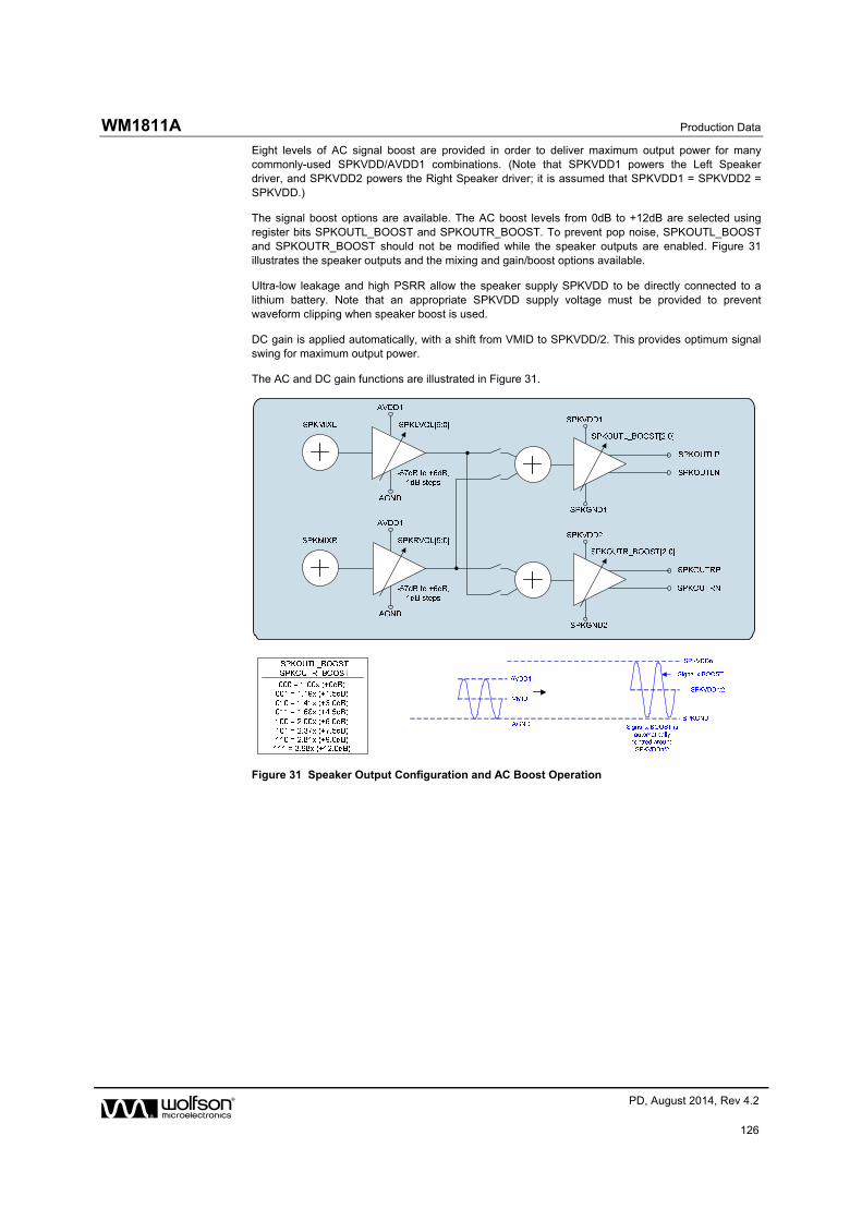
WM1811A Production Data
w PD, August 2014, Rev 4.2
126
Eight levels of AC signal boost are provided in order to deliver maximum output power for many commonly-used SPKVDD/AVDD1 combinations. (Note that SPKVDD1 powers the Left Speaker driver, and SPKVDD2 powers the Right Speaker driver; it is assumed that SPKVDD1 = SPKVDD2 = SPKVDD.)
The signal boost options are available. The AC boost levels from 0dB to +12dB are selected using register bits SPKOUTL_BOOST and SPKOUTR_BOOST. To prevent pop noise, SPKOUTL_BOOST and SPKOUTR_BOOST should not be modified while the speaker outputs are enabled. Figure 31 illustrates the speaker outputs and the mixing and gain/boost options available.
Ultra-low leakage and high PSRR allow the speaker supply SPKVDD to be directly connected to a lithium battery. Note that an appropriate SPKVDD supply voltage must be provided to prevent waveform clipping when speaker boost is used.
DC gain is applied automatically, with a shift from VMID to SPKVDD/2. This provides optimum signal swing for maximum output power.
The AC and DC gain functions are illustrated in Figure 31.
Figure 31 Speaker Output Configuration and AC Boost Operation

Production Data WM1811A
w PD, August 2014, Rev 4.2
127
REGISTER ADDRESS
BIT LABEL DEFAULT DESCRIPTION
R37 (0025h)
ClassD
5:3 SPKOUTL_BOOST[2:0]
000
(1.0x)
Left Speaker Gain Boost
000 = 1.00x boost (+0dB)
001 = 1.19x boost (+1.5dB)
010 = 1.41x boost (+3.0dB)
011 = 1.68x boost (+4.5dB)
100 = 2.00x boost (+6.0dB)
101 = 2.37x boost (+7.5dB)
110 = 2.81x boost (+9.0dB)
111 = 3.98x boost (+12.0dB)
2:0 SPKOUTR_BOOST[2:0]
000
(1.0x)
Right Speaker Gain Boost
000 = 1.00x boost (+0dB)
001 = 1.19x boost (+1.5dB)
010 = 1.41x boost (+3.0dB)
011 = 1.68x boost (+4.5dB)
100 = 2.00x boost (+6.0dB)
101 = 2.37x boost (+7.5dB)
110 = 2.81x boost (+9.0dB)
111 = 3.98x boost (+12.0dB)
R1825 (0721h)
Pull Control (2)
1 SPKMODE_PU 1 SPKMODE Pull-up enable
0 = Disabled
1 = Enabled
Table 72 Speaker Mode and Boost Control
Clocking of the Class D output driver is derived from SYSCLK. The clocking frequency division is configured automatically, according to the AIFn_SR and AIFnCLK_RATE registers. (See “Clocking and Sample Rates” for further details of the system clocks and control registers.)
The Class D switching clock is enabled whenever SPKOUTL_ENA or SPKOUTR_ENA is set. The frequency is as described in Table 73.
When AIF1CLK is selected as the SYSCLK source (SYSCLK_SRC = 0), then the Class D clock frequency is controlled by the AIF1_SR and AIF1CLK_RATE registers.
When AIF2CLK is selected as the SYSCLK source (SYSCLK_SRC = 1), then the Class D clock frequency is controlled by the AIF2_SR and AIF2CLK_RATE registers.
The applicable clocks (SYSCLK, AIF1CLK or AIF2CLK) must be present and enabled when using the speaker outputs in Class D mode. The presence of a suitable clock is automatically detected by the WM1811A; if the clock signal is absent, then the speaker outputs will be disabled.

WM1811A Production Data
w PD, August 2014, Rev 4.2
128
SAMPLE RATE (kHz)
SYSCLK RATE (AIFnCLK / fs ratio)
128 192 256 384 512 768 1024 1536
8 256 256 341.3 256 341.3 256 341.3 256
11.025 352.8 352.8 352.8 352.8 352.8 352.8 352.8
12 384 384 384 384 384 384 384
16 341.3 384 341.3 384 341.3 384
22.05 352.8 352.8 352.8 352.8 352.8
24 384 384 384 384 384
32 341.3 384 341.3 384
44.1 352.8 352.8 352.8
48 384 384 384
88.2 352.8
96 384
Table 73 Class D Switching Frequency (kHz)
HEADPHONE OUTPUT CONFIGURATIONS
The headphone outputs HPOUT1L andHPOUT1R are driven by the headphone output PGAs HPOUT1LVOL and HPOUT1RVOL. Each PGA has its own dedicated volume control, as described in the “Analogue Output Signal Path” section. The input to these PGAs can be either the output mixers MIXOUTL and MIXOUTR or the direct DAC outputs DACL and DACR.
The headphone output driver is capable of driving up to 30mW into a 16Ωload or 25mW into a 32Ωload such as a stereo headset or headphones. The outputs are ground-referenced, eliminating any requirement for AC coupling capacitors. This is achieved by having separate positive and negative supply rails powered by an on-chip charge pump.A DC Servo circuit removes any DC offset from the headphone outputs, suppressing ‘pop’ noiseand minimising power consumption. The Charge Pump and DC Servo are described separately (see “Charge Pump” and “DC Servo” respectively).
The typical headphone output connection is illustrated in Figure 32.
Figure 32 Headphone Output Configuration
The headphone output incorporates a common mode, or ground loop, feedback path which provides rejection of system-related ground noise. The return path is via HPOUT1FB. This pin must be connected to ground for normal operation of the headphone output. No register configuration is required.
Note that the HPOUT1FB pin should be connected to GND close to the headphone jack, as illustrated in Figure 32.

Production Data WM1811A
w PD, August 2014, Rev 4.2
129
EARPIECE DRIVER OUTPUT CONFIGURATIONS
The earpiece driver outputs HPOUT2P and HPOUT2N are driven by the HPOUT2MIX output mixer, which takes its inputs from the mixer output PGAs MIXOUTLVOL and MIXOUTRVOL. Fine volume control is available using MIXOUTLVOL and MIXOUTRVOL. A selectable -6dB attenuation is available on the HPOUT2MIX output, as described in Table 66 (refer to the “Analogue Output Signal Path” section).
The earpiece outputs are designed to operate in a BTL configuration, driving 50mW into a typical 16 ear speaker.
For suppression of pop noise there are two separate enables for the earpiece driver; HPOUT2_ENA enables the output stage and HPOUT2_IN_ENA enables the mixer and input stage. HPOUT2_IN_ENA should be enabled a minimum of 50s before HPOUT2_ENA.
LINE OUTPUT CONFIGURATIONS
The four line outputs LINEOUT1P, LINEOUT1N, LINEOUT2P and LINEOUT2N provide a highly flexible combination of differential and single-ended configurations, each driven by a dedicated output mixer.There is a selectable -6dB gain option in each mixer to avoid clipping when mixing more than one signal into a line output. Additional volume control is available at other locations within each of the supported signal paths. For more information about the line output mixing options, refer to the “Analogue Output Signal Path” section.
Typical applications for the line outputs (single-ended or differential) are:
Handset or headset microphone output to external voice CODEC
Stereo line output
Output to external speaker driver(s) to support additional loudspeakers
When single-ended mode is selected for either LINEOUT1 or LINEOUT2, a buffered VMID must be enabled as a reference for the outputs. This is enabled by setting the LINEOUT_VMID_BUF_ENA bit as defined in Table 74.
REGISTER ADDRESS
BIT LABEL DEFAULT DESCRIPTION
R56 (0038h)
AntiPOP (1)
7 LINEOUT_VMID_BUF_ENA
0 Enables VMID reference for line outputs in single-ended mode
0 = Disabled
1 = Enabled
Table 74 LINEOUT VMID Buffer for Single-Ended Operation
Some example line output configurations are listed and illustrated below.
Differential line output from Mic/Line input on IN1L PGA
Differential line output fromMic/Line input on IN1R PGA
Stereo differential line output from output mixers MIXOUTL and MIXOUTR
Stereo single-ended line output from output mixer to either LINEOUT1 or LINEOUT2
Mono single-ended line output from output mixer
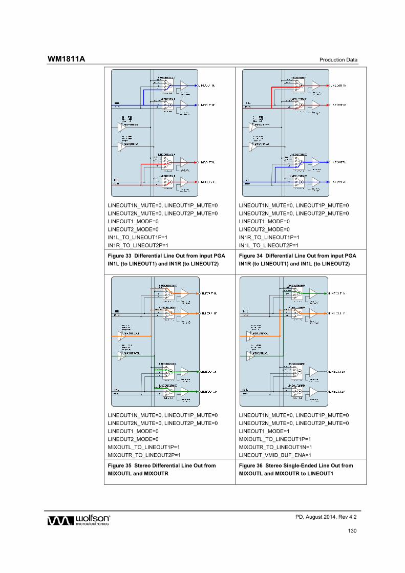
WM1811A Production Data
w PD, August 2014, Rev 4.2
130
LINEOUT1N_MUTE=0, LINEOUT1P_MUTE=0
LINEOUT2N_MUTE=0, LINEOUT2P_MUTE=0
LINEOUT1_MODE=0
LINEOUT2_MODE=0
IN1L_TO_LINEOUT1P=1
IN1R_TO_LINEOUT2P=1
LINEOUT1N_MUTE=0, LINEOUT1P_MUTE=0
LINEOUT2N_MUTE=0, LINEOUT2P_MUTE=0
LINEOUT1_MODE=0
LINEOUT2_MODE=0
IN1R_TO_LINEOUT1P=1
IN1L_TO_LINEOUT2P=1
Figure 33 Differential Line Out from input PGA
IN1L (to LINEOUT1) and IN1R (to LINEOUT2)
Figure 34 Differential Line Out from input PGA
IN1R (to LINEOUT1) and IN1L (to LINEOUT2)
LINEOUT1N_MUTE=0, LINEOUT1P_MUTE=0
LINEOUT2N_MUTE=0, LINEOUT2P_MUTE=0
LINEOUT1_MODE=0
LINEOUT2_MODE=0
MIXOUTL_TO_LINEOUT1P=1
MIXOUTR_TO_LINEOUT2P=1
LINEOUT1N_MUTE=0, LINEOUT1P_MUTE=0
LINEOUT2N_MUTE=0, LINEOUT2P_MUTE=0
LINEOUT1_MODE=1
MIXOUTL_TO_LINEOUT1P=1
MIXOUTR_TO_LINEOUT1N=1
LINEOUT_VMID_BUF_ENA=1
Figure 35 Stereo Differential Line Out from
MIXOUTL and MIXOUTR
Figure 36 Stereo Single-Ended Line Out from
MIXOUTL and MIXOUTR to LINEOUT1

Production Data WM1811A
w PD, August 2014, Rev 4.2
131
LINEOUT1N_MUTE=0, LINEOUT1P_MUTE=0
LINEOUT2N_MUTE=0, LINEOUT2P_MUTE=0
LINEOUT1_MODE=1
MIXOUTL_TO_LINEOUT2N=1
MIXOUTR_TO_LINEOUT2P=1
LINEOUT_VMID_BUF_ENA=1
LINEOUT1N_MUTE=0, LINEOUT1P_MUTE=0
LINEOUT2N_MUTE=0, LINEOUT2P_MUTE=0
LINEOUT1_MODE=1
LINEOUT2_MODE=1
MIXOUTL_TO_LINEOUT1N=1 and/or
MIXOUTL_TO_LINEOUT1P=1
MIXOUTR_TO_LINEOUT2N=1 and/or
MIXOUTR_TO_LINEOUT2P=1
LINEOUT_VMID_BUF_ENA=1
Figure 37 Stereo Single-Ended Line Out from
MIXOUTL and MIXOUTR to LINEOUT2
Figure 38 Mono Line Out to LINEOUT1N,
LINEOUT1P, LINEOUT2N, LINEOUT2P
The line outputs incorporate a common mode, or ground loop, feedback path which provides rejection of system-related ground noise. The return path, via LINEOUTFB, is enabled separately for LINEOUT1 and LINEOUT2 using the LINEOUT1_FB and LINEOUT2_FB bits as defined in Table 75.
Ground loop feedback is a benefit to single-ended line outputs only; it is not applicable to differential outputs, which already inherently offer common mode noise rejection.
REGISTER ADDRESS
BIT LABEL DEFAULT DESCRIPTION
R55 (0037h)
Additional Control
7 LINEOUT1_FB 0 Enable ground loop noise feedback on LINEOUT1
0 = Disabled
1 = Enabled
6 LINEOUT2_FB 0 Enable ground loop noise feedback on LINEOUT2
0 = Disabled
1 = Enabled
Table 75 Line Output Ground Loop Feedback Enable

WM1811A Production Data
w PD, August 2014, Rev 4.2
132
EXTERNAL ACCESSORY DETECTION
The WM1811A provides external accessory detection functions which can sense the presence and impedance of external components. This can be used to detect the insertion or removal of an external headphone or headset, and to provide an indication of key/button push events.
Jack insertion is detected using the JACKDET pin, which must be connected to switch contacts within the jack socket. An Interrupt event is generated whenever a jack insertion or jack removal event is detected.
Microphones, push-buttons and other accessories can be detected via the MICDET pin. The presence of a microphone, and the status of a hookswitch can be detected. This feature can also be used to detect push-button operation.
Note that clocking is required for all of the external accessory detection functions.The WM1811A can support accessory detection using a low frequency (eg. 32kHz) clock for reduced power consumption.
JACK DETECT
The WM1811A provides support for jack insertion switch detection. The Jack Detect function also enables the device to be configured for low power standby modes; typical use cases are where an application is idle in standby mode until a headphone or headset jack is inserted.
Jack insertion and removal is detected using the JACKDET pin. The recommended external connection circuit is illustrated in Figure 39. The status of the jack insertion switch can be read using the JACKDET_LVL register.
The JACKDET input de-bounce is enabled or disabled using the JACKDET_DB register, as described in Table 77.
The Jack Detect function is enabled whenever JACKDET_MODE > 00. An Interrupt Request (IRQ) event is generated whenever a jack insertion or jack removal is detected (see “Interrupts”).
Different settings of JACKDET_MODE allow different low power configurations to be selected. Note that audio and/or microphone detection functions are not supported under these low power conditions. The options provided by the JACKDET_MODE register are summarised in Table 76.
When JACKDET_MODE = 01, the LDO1 regulator output must be configured to be floating when disabled. The LDO1_DISCH bit (see Table 127) must be set to 0 before setting JACKDET_MODE = 01.
Note that, in modes where MICDET (microphone / accessory detect) functionality is required, this must be configured as described in the following section. In modes where the Audio functions are not supported, none of the WM1811A analogue/digital audio record or playback functions are possible.
JACKDET_MODE JACK DETECT MICROPHONE / ACCESSORY
DETECT
AUDIO FUNCTIONS
TYPICAL USE CASE
00 Full device operation (eg. audio record/playback). (Note that Jack Detect is not supported.)
01 Device in idle mode, monitoring accessory activity (eg. button press, jack removal etc.)
10 Device in standby mode, awaiting jack insertion -
Lowest power external accessory detection mode.
11 Full device operation (eg. audio record/playback).
Note that JACKDET_MODE = 01 or 10 are not supported if AVDD1 or DCVDD is supplied externally.
These settings must not be selected if AVDD1 or DCVDD is supplied externally (ie. if LDO1 or LDO2 is not used).
Table 76 Jack Detect Modes

Production Data WM1811A
w PD, August 2014, Rev 4.2
133
When JACKDET_MODE = 01, LDO1 and LDO2 are disabled. AVDD1 is powered from AVDD2, and DCVDD is powered from DBVDD1.
When JACKDET_MODE = 10, LDO1 and LDO2 are disabled. AVDD1 is unpowered, and DCVDD is powered from DBVDD1.
Note that, in both modes described above, the LDO1ENA input pin is ignored. The LDO2ENA pin must be asserted (logic ‘1’) to power DCVDD, although LDO2 will operate in a ‘bypass’ mode, connecting DCVDD to DBVDD1.
Note that, in both modes described above, the AVDD1 voltage is below the minimum recommended operating level. Analogue or digital audio functions cannot be supported in these modes.
Note that the LDO configuration for JACKDET_MODE = 01 or 10 assumes that AVDD1 and DCVDD are powered from LDO1 and LDO2 respectively. If AVDD1 or DCVDD is powered externally (not from the internal LDOs), then these settings of JACKDET_MODE must not be used.
If AVDD1 or DCVDD is powered externally (not from the internal LDOs), then the Jack Detect function, when required, should be enabled by setting JACKDET_MODE = 11.
The control registers associated with the Jack Detect function are described in Table 77.
REGISTER ADDRESS
BIT LABEL DEFAULT DESCRIPTION
R1797 (0705h)
JACKDET Ctrl
8 JACKDET_DB 1 JACKDETinput de-bounce
0 = Disabled
1 = Enabled
6 JACKDET_LVL 0 JACKDET input status
0 = Jack not detected
1 = Jack is detected
R57 (39h)
AntiPOP (2)
8:7 JACKDET_MODE 00 JACKDET mode select
00 = Jack Detect disabled
01 = Jack Detect enabled
10 = Jack Detect enabled
11 = Jack Detect enabled
MICDET (microphone/accessory detection) is not supported when JACKDET_MODE = 10.
Analogue/Digital audio functions are not supported when JACKDET_MODE = 01 or 10.
LDO1_DISCH must be set to 0 when JACKDET_MODE=01.
Settings 01 and 10 must not be selected if AVDD1 or DCVDD is supplied externally (ie. if LDO1 or LDO2 is not used).
Table 77 Jack Detect Control
Clocking for the jack detection function is derived from SYSCLK (defined in the “Clocking and Sample Rates” section). The WM1811A can support accessory detection using a low frequency (eg. 32kHz) clock for reduced power consumption. See the “External Accessory Detection Clocking” section below for further details.

WM1811A Production Data
w PD, August 2014, Rev 4.2
134
To configure the WM1811A in its lowest power condition, also supporting the Jack Detect function, the following actions are recommended:
Select lowest power Jack Detection mode (JACKDET_MODE = 10)
Select 32kHz SYSCLK
Disable the Thermal sensor (TSHUT_ENA = 0)
Configure LDO1 output to float when disabled (LDO1_DISCH = 0)
Minimise any static current leakage paths on digital inputs where internal pull-up or pull-down resistors are enabled (ie. disable the pull-up/pull-down resistors on these inputs)
Care should be taken to restore all applicable device settings when normal operation is resumed following the low power jack detection. In particular, note that the thermal sensor should be enabled for normal operation.
A recommended connection circuit, including headphone output on HPOUT1 and microphone connections, is shown in Figure 39. See “Applications Information” for details of recommended external components.
Figure 39 Jack Detect and External Accessory Connections
The internal comparator circuit used to detect the JACKDET status is illustrated in Figure 40.
The threshold voltages for the jack detect circuit are noted in the “Electrical Characteristics”. Note that separate thresholds are defined for jack insertion and jack removal.
JACKDET+- reference
AVDD2
Jack Detect logic
1M
(jack insertion switch)
Note: The illustrated circuit assumes the jack insertion switch contacts are closed when jack is inserted.
WM1811A
Figure 40 Jack Detect Comparator
Production Data WM1811A
w PD, August 2014, Rev 4.2
135
MICROPHONE / ACCESSORY DETECT
The WM1811A accessory detection circuit measures the impedance of an external load connected to the MICDET pin. This feature can be used to detect the insertion or removal of a microphone, and the status of the associated hookswitch. It can also be used to detect push-button status or the connection of other external accessories.
The microphone detection circuit measures the impedance connected to MICDET, and reports whether the measured impedance lies within one of 9 pre-defined levels (including the ‘no accessory detected’ level). This means it can detect the presence of a typical microphone and up to 7 push-buttons. One of the impedance levels is specifically designed to detect a video accessory (typical 75) load if required.
The microphone detection circuit uses the MICBIAS2 output as a reference. The WM1811A will automatically enable MICBIAS2 when required in order to perform the detection function; this allows the detection function to be supported in low-power standby operating conditions.
Microphone detection is enabled by setting the MICD_ENA register. When microphone detection is enabled, the WM1811A performs a number of measurements in order to determine the MICDET impedance. The measurement process is repeated at a cyclic rate controlled by MICD_RATE.(The MICD_RATE register selects the delay between completion of one measurement and the start of the next.)
For best accuracy, the measured impedance is only deemed valid after more than one successive measurement has produced the same result. The MICD_DBTIME register provides control of the de-bounce period; this can be either 2 measurements or 4 measurements.
When the microphone detection result has settled (ie. after the applicable de-bounce period), the WM1811A indicates valid data by setting the MICD_VALID bit. The measured impedance is indicated using the MICD_LVL and MICD_STS register bits, as described in Table 78.
The MICD_VALID bit, when set, remains asserted for as long as the microphone detection function is enabled (ie. while MICD_ENA = 1). If the detected impedance changes, then the MICD_LVL and MICD_STS fields will change, but the MICD_VALID bit will remain set, indicating valid data at all times.
Note that the impedance levels quoted in the MICD_LVL description assume that a microphone (475Ω to 30kΩ impedance) is also present on the MICDET pin. The limits quoted in the “Electrical Characteristics” refer to the combined effective impedance on the MICDET pin. Typical external components are described in the “Applications Information” section.
The microphone detection reports a measurement result in one of the pre-defined impedance levels. Each measurement level can be enabled or disabled independently; this provides flexibility according to the required thresholds, and offers a faster measurement time in some applications. The MICD_LVL_SEL register is described in detail later in this section.
Clocking for the microphone detection function is derived from SYSCLK (defined in the “Clocking and Sample Rates” section).The WM1811A can support accessory detection using a low frequency (eg. 32kHz) clock for reduced power consumption. See the “External Accessory Detection Clocking” section below for further details.
The microphone detection function is an input to the Interrupt control circuit and can be used to trigger an Interrupt event every time an accessory insertion, removal or impedance change is detected. See “Interrupts” for further details.
The microphone detection function can also generate a GPIO output, providing an external indication of the microphone detection. This GPIO output is pulsed every time an accessory insertion, removal or impedance change is detected. See “General Purpose Input/Output” for details of how to configure a GPIO pin to output the microphone detection signal.
The register fields associated with Microphone Detection (or other accessories) are described in Table 78. The external circuit configuration is illustrated in Figure 41.

WM1811A Production Data
w PD, August 2014, Rev 4.2
136
REGISTER ADDRESS
BIT LABEL DEFAULT DESCRIPTION
R208 (00D0h)
Mic Detect 1
15:12 MICD_BIAS_STARTTIME [3:0]
0111 Mic Detect Bias Startup Delay
(If MICBIAS2 is not enabled already, this field selects the delay time allowed for MICBIAS2 to startup prior to performing the MICDET function.)
0000 = 0ms (continuous)
0001 = 0.25ms
0010 = 0.5ms
0011 = 1ms
0100 = 2ms
0101 = 4ms
0110 = 8ms
0111 = 16ms
1000 = 32ms
1001 = 64ms
1010 = 128ms
1011 = 256ms
1100 to 1111 = 512ms
11:8 MICD_RATE [3:0] 0110 Mic Detect Rate
(Selects the delay between successive Mic Detect measurements.)
0000 = 0ms (continuous)
0001 = 0.25ms
0010 = 0.5ms
0011 = 1ms
0100 = 2ms
0101 = 4ms
0110 = 8ms
0111 = 16ms
1000 = 32ms
1001 = 64ms
1010 = 128ms
1011 = 256ms
1100 to 1111 = 512ms
1 MICD_DBTIME 0 Mic Detect De-bounce
0 = 2 measurements
1 = 4 measurements
0 MICD_ENA 0 Mic Detect Enable
0 = Disabled
1 = Enabled
Note that Mic Detect is not supported when JACKDET_MODE = 10.
Production Data WM1811A
w PD, August 2014, Rev 4.2
137
REGISTER ADDRESS
BIT LABEL DEFAULT DESCRIPTION
R209 (00D1h)
Mic Detect 2
7:0 MICD_LVL_SEL [7:0]
0111_
1111
Mic Detect Level Select
(enables Mic Detection in specific impedance ranges)
[7] = Not used - must be set to 0
[6] = Enable >475 ohm detection
[5] = Enable 326 ohm detection
[4] = Enable 152 ohm detection
[3] = Enable 77 ohm detection
[2] = Enable 47.6 ohm detection
[1] = Enable 29.4 ohm detection
[0] = Enable 14 ohm detection
Note that the impedance values quoted assume that a microphone (475ohm-30kohm) is also present on the MICDET pin.
R210 (00D2h)
Mic Detect 3
10:2 MICD_LVL [8:0] 0_0000_
0000
Mic Detect Level
(indicates the measured impedance)
[8] = Not used
[7] = >475 ohm, <30k ohm
[6] = 326 ohm
[5] = 152 ohm
[4] = 77 ohm
[3] = 47.6 ohm
[2] = 29.4 ohm
[1] = 14 ohm
[0] = <3 ohm
Note that the impedance values quoted assume that a microphone (475ohm-30kohm) is also present on the MICDET pin.
1 MICD_VALID 0 Mic Detect Data Valid
0 = Not Valid
1 = Valid
0 MICD_STS 0 Mic Detect Status
0 = No Mic Accessory present (impedance is >30k ohm)
1 = Mic Accessory is present
(impedance is <30k ohm)
Table 78 Microphone Detect Control

WM1811A Production Data
w PD, August 2014, Rev 4.2
138
The external connections for the Microphone Detect circuit are illustrated in Figure 41. In typical applications, it can be used to detect a microphone or button press.
The microphone detection function uses MICBIAS2 as a reference. The microphone detection function will automatically enable MICBIAS2 when required for MICDET impedance measurement.
If MICBIAS2 is not already enabled (ie. if MICB2_ENA = 0), then MICBIAS2 will be enabled for short periods of time only, every time the impedance measurement is scheduled. To allow time for the MICBIAS2 source to start-up, a time delay is applied before the measurement is performed; this is configured using the MICD_BIAS_STARTTIME register, as described in Table 78.
The MICD_BIAS_STARTTIME register should be set to 16ms or more if MICB2_RATE = 1 (pop-free start-up / shut-down). The MICD_BIAS_STARTTIME register should be set to 0.25ms or more if MICB2_RATE = 0 (fast start-up / shut-down).
If the MICBIAS2 reference is not enabled continuously (ie. if MICB2_ENA = 0), then the MICBIAS2 discharge bit (MICB2_DISCH) should be set to 0.
The MICBIAS sources are configured using the registers described in Table 1, in the “Analogue Input Signal Path” section.
Figure 41 Microphone Detect Interface
The MICD_LVL_SEL [7:0] register bits allow each of the impedance measurement levels to be enabled or disabled independently. This allows the function to be tailored to the particular application requirements.
If one or more bits within the MICD_LVL_SEL register is set to 0, then the corresponding impedance levelwill be disabled. Any measured impedance which lies in a disabled level will be reported as the next lowest, enabled level.
For example, the MICD_LVL_SEL [3] bit enables the detection of impedances around 77. If MICD_LVL_SEL [3] = 0, then an external impedance of 77 will not be indicated as 77 but will be indicated as 47; this would be reported in the MICD_LVL register as MICD_LVL [3] = 1.
With all measurement levels enabled, the WM1811A can detect the presence of a typical microphone and up to 7 push-buttons. The microphone detect function is specifically designed to detect a video accessory (typical 75) load if required.
See “Applications Information” for typical recommended external components for microphone, video or push-button accessory detection.
The microphone detection circuit assumes that a 2.2k(2%) resistor is connected to MICBIAS2, as illustrated. Different resistor values will lead to inaccuracy in the impedance measurement.

Production Data WM1811A
w PD, August 2014, Rev 4.2
139
The measurement accuracy of the microphone detect function is assured whenever the connected load is within the applicable limits specified in the “Electrical Characteristics”. Note that a 2.2k (2%) resistor must also be connected between MICDET and MICBIAS2.
Note that the connection of a microphone will change the measured impedance on the MICDET pin; see “Applications Information” for recommended components for typical applications.
The measurement time varies between 100s and 500s according to the impedance of the external load. A high impedance will be measured faster than a low impedance.
The timing of the microphone detect function is illustrated in Figure 42. Two different cases are shown, according to whether MICBIAS2 is enabled periodically by the impedance measurement function (MICB2_ENA=0), or is enabled at all times (MICB2_ENA=1).
Figure 42 Microphone Detect Timing

WM1811A Production Data
w PD, August 2014, Rev 4.2
140
EXTERNAL ACCESSORY DETECTION CLOCKING
Clocking for the jack detect and microphone detection functions is derived from SYSCLK (defined in the “Clocking and Sample Rates” section).
When AIF1CLK is selected as the SYSCLK source (SYSCLK_SRC = 0), then AIF1CLK must be present and enabled when using the external accessory detect functions. The AIF1_SR and AIF1CLK_RATE registers must be set to values that are consistent with the available AIF1CLK frequency.
When AIF2CLK is selected as the SYSCLK source (SYSCLK_SRC = 1), then AIF2CLK must be present and enabled when using the external accessory detect functions.The AIF2_SR and AIF2CLK_RATE registers must be set to values that are consistent with the available AIF2CLK frequency.
The accessory detection functions can also be supported using a low frequency (eg. 32kHz) clock, as described below - see “External Accessory Detection with Low Frequency SYSCLK”.
The Frequency Locked Loop (FLL) free-running mode provides flexibility to clock the accessory detection functions without any external reference clock, eg. in low-power standby operating conditions. See “Clocking and Sample Rates” for details of the WM1811A clocking options and FLL.
EXTERNAL ACCESSORY DETECTION WITH LOW FREQUENCY SYSCLK
Clocking for the jack detect and microphone detection function can be derived from AIF1CLK or AIF2CLK, as described earlier.
Under normal circumstances, the AIFn_SR and AIFnCLK_RATE registers must be set to values that are consistent with the available AIFnCLK frequency. The register settings support AIFnCLK frequencies of 1.024MHz or higher.
The microphone detection function can also be supported using a low frequency (eg. 32kHz) clock. In this case, the selected SYSCLK source (AIF1CLK or AIF2CLK) should be configured with the following register settings:
AIFnCLK_RATE = 0001 (AIFnCLK / fs = 128)
AIFn_SR = 0000 (fs = 8kHz)
The register settings above configure the WM1811A for AIFnCLK = 1.024MHz. If the available clock is a different frequency (eg. 32kHz), then the timings set by the MICD_RATE and MICD_BIAS_STARTUP registers will be scaled accordingly. In the case of a 32kHz clock, these times will be extended by a factor of 32 (calculated as 1024000 / 32000).
For example, under normal circumstances, setting MICD_RATE = 0011 selects a 1ms delay between successive measurements. Using a 32kHz reference clock, and the register settings above, then MICD_RATE = 0011 will select a 32ms delay.

Production Data WM1811A
w PD, August 2014, Rev 4.2
141
GENERAL PURPOSE INPUT/OUTPUT
The WM1811A provides a number of GPIO functions to enable interfacing and detection of external hardware and to provide logic outputs to other devices. The input functions can be polled directly or can be used to generate an Interrupt (IRQ) event. The GPIO and Interrupt circuits support the following functions:
Alternate interface functions (AIF3)
Button detect (GPIO input)
Logic ‘1’ and logic ‘0’ output (GPIO output)
Interrupt (IRQ) status output
Over-Temperature detection
Microphone accessory status detection
Frequency Locked Loop (FLL) Lock status output
Sample Rate Conversion (SRC) Lock status output
Dynamic Range Control (DRC) Signal activity detection
Digital Core FIFO error status output
Clock output (SYSCLK divided by OPCLK_DIV)
Frequency Locked Loop (FLL) Clock output
GPIO CONTROL
For each GPIO, the selected function is determined by the GPn_FN field, where n identifies the GPIO pin (1, 8, 9, 10, 11). The pin direction, set by GPn_DIR, must be set according to function selected by GPn_FN.
The digital audio interface AIF3 is supported using GPIO pins; the applicable pin functions are selected by setting the corresponding GPn_FN register to 00h. The ADCLRCLK1 function for AIF1 is supported on GPIO1. See Table 80 for the definition of which AIF function is available on each GPIO pin.
See “Digital Audio Interface Control” for details of AIF2 and AIF3.
When a pin is configured as a GPIO input (GPn_DIR = 1), the logic level at the pin can be read from the respective GPn_LVL bit. Note that GPn_LVL is not affected by the GPn_POL bit.
A de-bounce circuit can be enabled on any GPIO input, to avoid false event triggers. This is enabled on each pin by setting the respective GPn_DB bit.
When a pin is configured as a Logic Level output (GPn_DIR = 0, GPn_FN = 01h), its level can be set to logic 0 or logic 1 using the GPn_LVL field.
When a pin is configured as an output (GPn_DIR = 0), the polarity can be inverted using the GPn_POL bit. When GPn_POL = 1, then the selected output function is inverted. In the case of Logic Level output (GPn_FN = 01h), the external output will be the opposite logic level to GPn_LVL when GPn_POL = 1.
A GPIO output can be either CMOS driven or Open Drain. This is selected on each pin using the respective GPn_OP_CFG bit.
Internal pull-up and pull-down resistors may be enabled using the GPn_PU and GPn_PD fields; this allows greater flexibility to interface with different signals from other devices.(Note that if GPn_PU and GPn_PD are both set for any GPIO pin, then the pull-up and pull-down will be disabled.)
Each of the GPIO pins is an input to the Interrupt control circuit and can be used to trigger an Interrupt event. An interrupt event is triggered on the rising and falling edge of the GPIO input. The associated interrupt bit is latched once set; it can be polled at any time or used to control the IRQ signal. See “Interrupts” for more details of the Interrupt event handling.

WM1811A Production Data
w PD, August 2014, Rev 4.2
142
The register fields that control the GPIO pins are described inTable 79.
REGISTER ADDRESS
BIT LABEL DEFAULT DESCRIPTION
R1792 (0700h)
GPIO1
R1799 (0707h)
GPIO8
to
R1802 (070Ah)
GPIO11
15 GPn_DIR 1 GPIOn Pin Direction
0 = Output
1 = Input
14 GPn_PU 0 GPIOnPull-Up Enable
0 = Disabled
1 = Enabled
13 GPn_PD 1 GPIOn Pull-Down Enable
0 = Disabled
1 = Enabled
10 GPn_POL 0 GPIOn Polarity Select
0 = Non-inverted (Active High)
1 = Inverted (Active Low)
9 GPn_OP_CFG 0 GPIOn Output Configuration
0 = CMOS
1 = Open Drain
8 GPn_DB 1 GPIOn Input De-bounce
0 = Disabled
1 = Enabled
6 GPn_LVL 0 GPIOn level. Write to this bit to set a GPIO output. Read from this bit to read GPIO input level.
For output functions only, when GPn_POL is set, the register contains the opposite logic level to the external pin.
4:0 GPn_FN [4:0] GPIOn Pin Function
(see Table 80 for details)
GP1_FN default = 0000
GP8_FN default = 0001
GP9_FN default = 0001
GP10_FN default = 0001
GP11_FN default = 0001
Note:n is a number (1, 8, 9, 10, 11) that identifies the individual GPIO.
Table 79 GPIO1, GPIO8, GPIO9, GPIO10 to GPIO11 Control
GPIO FUNCTION SELECT
The available GPIO functions are described in Table 80. The function of each GPIO is set using the GPn_FN register, where n identifies the GPIO pin (1, 8, 9, 10, 11). Note that the respective GPn_DIR must also be set according to whether the function is an input or output.
GPn_FN DESCRIPTION COMMENTS
00h GPIO1 - ADCLRCLK1
GPIO8 - DACDAT3
GPIO9 - ADCDAT3
GPIO10 - LRCLK3
GPIO11 - BCLK3
Alternate Audio Interface connections.
01h Button detect input / Logic level output
GPn_DIR = 0: GPIO pin logic level is set by GPn_LVL.
GPn_DIR = 1: Button detect or logic level input.
02h Reserved
03h IRQ Interrupt (IRQ) output
0 = IRQ not asserted
1 = IRQ asserted

Production Data WM1811A
w PD, August 2014, Rev 4.2
143
GPn_FN DESCRIPTION COMMENTS
04h Temperature (Shutdown) status output
Indicates Temperature Shutdown Sensor status
0 = Temperature is below shutdown level
1 = Temperature is above shutdown level
05h Microphone Detect Microphone Detect (MICDET accessory) IRQ output
A single 31s pulse is output whenever an accessory insertion, removal or impedance change is detected.
06h Reserved
07h Reserved
08h Reserved
09h FLL1 Lock Indicates FLL1 Lock status
0 = Not locked
1 = Locked
0Ah FLL2 Lock Indicates FLL2 Lock status
0 = Not locked
1 = Locked
0Bh SRC1 Lock Indicates SRC1 Lock status
0 = Not locked
1 = Locked
0Ch SRC2 Lock Indicates SRC2 Lock status
0 = Not locked
1 = Locked
0Dh AIF1 DRC1 Signal Detect
Indicates AIF1 DRC Signal Detect status
0 = Signal threshold not exceeded
1 = Signal threshold exceeded
0Eh Reserved
0Fh AIF2 DRC Signal Detect
Indicates AIF2 DRC Signal Detect status
0 = Signal threshold not exceeded
1 = Signal threshold exceeded
10h Reserved
11h FIFO Error Indicates a Digital Core FIFO Error condition
0 = Normal operation
1 = FIFO Error
12h Clock Output OPCLK GPIO Clock derived from SYSCLK
13h Temperature (Warning) status output
Indicates Temperature Warning Sensor status
0 = Temperature is below warning level
1 = Temperature is above warning level
14h DC Servo Done Indicates DC Servo status on HPOUT1L and HPOUT1R
0 = DC Servo not complete
1 = DC Servo complete
15h FLL1 Clock Output Clock output from FLL1
16h FLL2 Clock Output Clock output from FLL2
17h to 1Fh Reserved
Table 80 GPIO Function Select

WM1811A Production Data
w PD, August 2014, Rev 4.2
144
BUTTON DETECT (GPIO INPUT)
Button detect functionality can be selected on any GPIO pin by setting the respective GPIO registers as described in “GPIO Control”. The same functionality can be used to support a Jack Detect input function.
It is recommended to enable the GPIO input de-bounce feature when using GPIOs as button input or Jack Detect input.
The GPn_LVL fields may be read to determine the logic levels on a GPIO input, after the selectable de-bounce controls.Note that GPn_LVL is not affected by the GPn_POL bit.
The de-bounced GPIO signals are also inputs to the Interrupt control circuit. An interrupt event is triggered on the rising and falling edge of the GPIO input. The associated interrupt bits are latched once set; it can be polled at any time or used to control the IRQ signal. See “Interrupts” for more details of the Interrupt event handling.
LOGIC ‘1’ AND LOGIC ‘0’ OUTPUT (GPIO OUTPUT)
The WM1811A can be programmed to drive a logic high or logic low level on any GPIO pin by selecting the “GPIO Output” function as described in “GPIO Control”. The output logic level is selected using the respective GPn_LVL bit.
Note that the polarity of the GPIO output can be inverted using the GPn_POL registers. If GPn_POL = 1, then the external output will be the opposite logic level to GPn_LVL.
INTERRUPT (IRQ) STATUS OUTPUT
The WM1811A has an Interrupt Controller which can be used to indicate when any selected Interrupt events occur. An interrupt can be generated by any of the events described throughout the GPIO function definition above. Individual interrupts may be masked in order to configure the Interrupt as required. See “Interrupts” for further details.
The Interrupt (IRQ) status may be output directly on any GPIO pin by setting the respective GPIO registers as described in “GPIO Control”.
OVER-TEMPERATURE DETECTION
The WM1811A incorporates a temperature sensor which detects when the device temperature is within normal limits or if the device is approaching a hazardous temperature condition.
The Temperature status may be output directly on any GPIO pin by setting the respective GPIO registers as described in “GPIO Control”. Any GPIO pin can be used to indicate either a Warning Temperature event or the Shutdown Temperature event. De-bounce can be applied to the applicable signal using the register bits described in Table 81.
The Warning Temperature and Shutdown Temperature status are inputs tothe Interrupt control circuit, after the selectable de-bounce. An interrupt event may be triggered on the rising and falling edges of these signals. The associated interrupt bit is latched once set; it can be polled at any time or used to control the IRQ signal. See “Interrupts” for more details of the Interrupt event handling.
Note that the temperature sensor can be configured to automatically disable the audio outputs of the WM1811A (see “Thermal Shutdown”). In some applications, it may be preferable to manage the temperature sensor event through GPIO or Interrupt functions, allowing a host processor to implement a controlled system response to an over-temperature condition.
The temperature sensor must be enabled by setting the TSHUT_ENA register bit. When the TSHUT_OPDIS is also set, then a device over-temperature condition will cause the speaker outputs (SPKOUTL and SPKOUTR) of the WM1811A to be disabled.
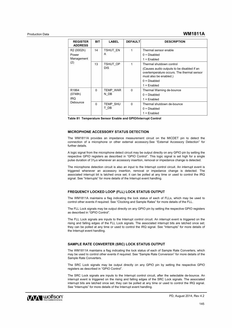
Production Data WM1811A
w PD, August 2014, Rev 4.2
145
REGISTER ADDRESS
BIT LABEL DEFAULT DESCRIPTION
R2 (0002h)
Power Management (2)
14 TSHUT_ENA
1 Thermal sensor enable
0 = Disabled
1 = Enabled
13 TSHUT_OPDIS
1 Thermal shutdown control
(Causes audio outputs to be disabled if an overtemperature occurs. The thermal sensor must also be enabled.)
0 = Disabled
1 = Enabled
R1864 (0748h)
IRQ Debounce
0 TEMP_WARN_DB
0 Thermal Warning de-bounce
0 = Disabled
1 = Enabled
0 TEMP_SHUT_DB
0 Thermal shutdown de-bounce
0 = Disabled
1 = Enabled
Table 81 Temperature Sensor Enable and GPIO/Interrupt Control
MICROPHONE ACCESSORY STATUS DETECTION
The WM1811A provides an impedance measurement circuit on the MICDET pin to detect the connection of a microphone or other external accessory.See “External Accessory Detection” for further details.
A logic signal from the microphone detect circuit may be output directly on any GPIO pin by setting the respective GPIO registers as described in “GPIO Control”. This logic signal is set high for a single pulse duration of 31s whenever an accessory insertion, removal or impedance change is detected.
The microphone detection circuit is also an input to the Interrupt control circuit. An interrupt event is triggered whenever an accessory insertion, removal or impedance change is detected. The associated interrupt bit is latched once set; it can be polled at any time or used to control the IRQ signal. See “Interrupts” for more details of the Interrupt event handling.
FREQUENCY LOCKED LOOP (FLL) LOCK STATUS OUTPUT
The WM1811A maintains a flag indicating the lock status of each of FLLs, which may be used to control other events if required. See “Clocking and Sample Rates” for more details of the FLL.
The FLL Lock signals may be output directly on any GPIO pin by setting the respective GPIO registers as described in “GPIO Control”.
The FLL Lock signals are inputs to the Interrupt control circuit. An interrupt event is triggered on the rising and falling edges of the FLL Lock signals. The associated interrupt bits are latched once set; they can be polled at any time or used to control the IRQ signal. See “Interrupts” for more details of the Interrupt event handling.
SAMPLE RATE CONVERTER (SRC) LOCK STATUS OUTPUT
The WM1811A maintains a flag indicating the lock status of each of Sample Rate Converters, which may be used to control other events if required. See “Sample Rate Conversion” for more details of the Sample Rate Converters.
The SRC Lock signals may be output directly on any GPIO pin by setting the respective GPIO registers as described in “GPIO Control”.
The SRC Lock signals are inputs to the Interrupt control circuit, after the selectable de-bounce. An interrupt event is triggered on the rising and falling edges of the SRC Lock signals. The associated interrupt bits are latched once set; they can be polled at any time or used to control the IRQ signal. See “Interrupts” for more details of the Interrupt event handling.
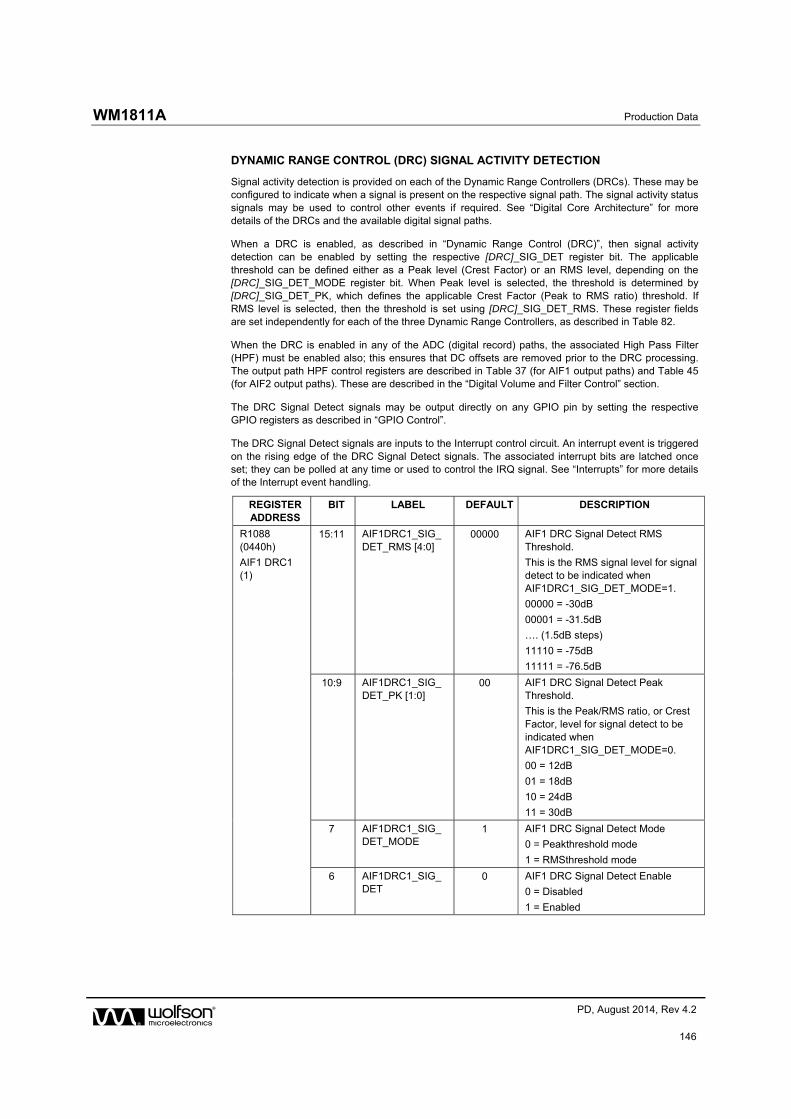
WM1811A Production Data
w PD, August 2014, Rev 4.2
146
DYNAMIC RANGE CONTROL (DRC) SIGNAL ACTIVITY DETECTION
Signal activity detection is provided on each of the Dynamic Range Controllers (DRCs). These may be configured to indicate when a signal is present on the respective signal path. The signal activity status signals may be used to control other events if required. See “Digital Core Architecture” for more details of the DRCs and the available digital signal paths.
When a DRC is enabled, as described in “Dynamic Range Control (DRC)”, then signal activity detection can be enabled by setting the respective [DRC]_SIG_DET register bit. The applicable threshold can be defined either as a Peak level (Crest Factor) or an RMS level, depending on the [DRC]_SIG_DET_MODE register bit. When Peak level is selected, the threshold is determined by [DRC]_SIG_DET_PK, which defines the applicable Crest Factor (Peak to RMS ratio) threshold. If RMS level is selected, then the threshold is set using [DRC]_SIG_DET_RMS. These register fields are set independently for each of the three Dynamic Range Controllers, as described in Table 82.
When the DRC is enabled in any of the ADC (digital record) paths, the associated High Pass Filter (HPF) must be enabled also; this ensures that DC offsets are removed prior to the DRC processing. The output path HPF control registers are described in Table 37 (for AIF1 output paths) and Table 45 (for AIF2 output paths). These are described in the “Digital Volume and Filter Control” section.
The DRC Signal Detect signals may be output directly on any GPIO pin by setting the respective GPIO registers as described in “GPIO Control”.
The DRC Signal Detect signals are inputs to the Interrupt control circuit. An interrupt event is triggered on the rising edge of the DRC Signal Detect signals. The associated interrupt bits are latched once set; they can be polled at any time or used to control the IRQ signal. See “Interrupts” for more details of the Interrupt event handling.
REGISTER ADDRESS
BIT LABEL DEFAULT DESCRIPTION
R1088 (0440h)
AIF1 DRC1 (1)
15:11 AIF1DRC1_SIG_DET_RMS [4:0]
00000 AIF1 DRC Signal Detect RMS Threshold.
This is the RMS signal level for signal detect to be indicated when AIF1DRC1_SIG_DET_MODE=1.
00000 = -30dB
00001 = -31.5dB
…. (1.5dB steps)
11110 = -75dB
11111 = -76.5dB
10:9 AIF1DRC1_SIG_DET_PK [1:0]
00 AIF1 DRC Signal Detect Peak Threshold.
This is the Peak/RMS ratio, or Crest Factor, level for signal detect to be indicated when AIF1DRC1_SIG_DET_MODE=0.
00 = 12dB
01 = 18dB
10 = 24dB
11 = 30dB
7 AIF1DRC1_SIG_DET_MODE
1 AIF1 DRC Signal Detect Mode
0 = Peakthreshold mode
1 = RMSthreshold mode
6 AIF1DRC1_SIG_DET
0 AIF1 DRC Signal Detect Enable
0 = Disabled
1 = Enabled

Production Data WM1811A
w PD, August 2014, Rev 4.2
147
REGISTER ADDRESS
BIT LABEL DEFAULT DESCRIPTION
R1344 (0540h)
AIF2 DRC (1)
15:11 AIF2DRC_SIG_DET_RMS [4:0]
00000 AIF2 DRC Signal Detect RMS Threshold.
This is the RMS signal level for signal detect to be indicated when AIF2DRC_SIG_DET_MODE=1.
00000 = -30dB
00001 = -31.5dB
…. (1.5dB steps)
11110 = -75dB
11111 = -76.5dB
10:9 AIF2DRC_SIG_DET_PK [1:0]
00 AIF2 DRC Signal Detect Peak Threshold.
This is the Peak/RMS ratio, or Crest Factor, level for signal detect to be indicated when AIF2DRC_SIG_DET_MODE=0.
00 = 12dB
01 = 18dB
10 = 24dB
11 = 30dB
7 AIF2DRC_SIG_DET_MODE
1 AIF2 DRC Signal Detect Mode
0 = Peakthreshold mode
1 = RMSthreshold mode
6 AIF2DRC_SIG_DET
0 AIF2 DRC Signal Detect Enable
0 = Disabled
1 = Enabled
Table 82 DRC Signal Activity Detect GPIO/Interrupt Control
DIGITAL CORE FIFO ERROR STATUS DETECTION
The WM1811A monitors the Digital Core for error conditions which may occur if a clock rate mismatch is detected. Under these conditions, the digital audio may become corrupted.
The most likely cause of a Digital Core FIFO Error condition is an incorrect system clocking configuration. See “Clocking and Sample Rates” for the WM1811A system clocking requirements.
The Digital Core FIFO Error function is provided in order that the systemconfiguration can be verified during product development.
The FIFO Error signal may be output directly on any GPIO pin by setting the respective GPIO registers as described in “GPIO Control”.
The FIFO Error signal is an input to the Interrupt control circuit. An interrupt event is triggered on the rising edge of the FIFO Error signal. The associated interrupt bit is latched once set; it can be polled at any time or used to control the IRQ signal. See “Interrupts” for more details of the Interrupt event handling.

WM1811A Production Data
w PD, August 2014, Rev 4.2
148
OPCLK CLOCK OUTPUT
A clock output (OPCLK) derived from SYSCLK may be output on any GPIO pin by setting the respective GPIO registers as described in “GPIO Control”. This clock is enabled by register bit OPCLK_ENA, and its frequency is controlled by OPCLK_DIV.
See “Clocking and Sample Rates” for more details of the System Clock (SYSCLK).
REGISTER ADDRESS
BIT LABEL DEFAULT DESCRIPTION
R2 (0002h)
Power Management (2)
11 OPCLK_ENA
0 GPIO Clock Output (OPCLK) Enable
0 = Disabled
1 = Enabled
R521 (0209h)
Clocking 1
2:0 OPCLK_DIV 000 GPIO Output Clock (OPCLK) Divider
000 = SYSCLK
001 = SYSCLK / 2
010 = SYSCLK / 3
011 = SYSCLK / 4
100 = SYSCLK / 6
101 = SYSCLK / 8
110 = SYSCLK / 12
111 = SYSCLK / 16
Table 83 OPCLK Control
FLL CLOCK OUTPUT
The FLL Clock outputs may be outputdirectly on any GPIO pin by setting the respective GPIO registers as described in “GPIO Control”.
See “Clocking and Sample Rates” for more details of the WM1811A system clocking and for details of how to enable and configure the Frequency Locked Loops.

Production Data WM1811A
w PD, August 2014, Rev 4.2
149
INTERRUPTS
The Interrupt Controller has multiple inputs. These include the GPIO input pins, the FLL Lock circuits, SRC Lock circuit, Microphone activity detection, Over-temperature indication and Digital FIFO error detection. Any combination of these inputs can be used to trigger an Interrupt Request (IRQ) event.
There is an Interrupt register field associated with each of the interrupt inputs. These fields are asserted whenever a logic edge is detected on the respective input. Some inputs are triggered on rising edges only; some are triggered on both edges, as noted in Table 84. The Interrupt register fields are held in Registers R1840 and R1841. The Interrupt flags can be polled at any time from these registers, or else in response to the Interrupt Request (IRQ) output being signalled via a GPIO pin.
All of the Interrupts are edge-triggered, as noted above. Many of these are triggered on both the rising and falling edges and, therefore, the Interrupt registers cannot indicate which edge has been detected. The “Raw Status” fields in Register R1842 provide readback of the current value of selected inputs to the Interrupt Controller. Note that the logic levels of any GPIO inputs can be read using the GPn_LVL registers, as described in Table 79.
Individual mask bits can select or deselect different functions from the Interrupt controller. These are listed within the Interrupt Status Mask registers, as described in Table 84. Note that the Interrupt register fields remain valid, even when masked, but the masked interrupts will not cause the Interrupt Request (IRQ) output to be asserted.
The Interrupt Request (IRQ) output represents the logical ‘OR’ of all the unmasked interrupts. The Interrupt register fields are latching fields and, once they are set, they are not reset until a ‘1’ is written to the respective register bit(s). The Interrupt Request (IRQ) output is not reset until each of the unmasked interrupts has been reset.
De-bouncing of the GPIO inputs can be enabled using the register bits described in Table 79. De-bouncing is also available on the Temperature Warning and Temperature Shutdown inputs to the Interrupt Controller, in order to avoid false detections - see Table 84 for the associated registers.
The Interrupt Request (IRQ) output can be globally masked by setting the IM_IRQ register. Under default conditions, the Interrupt Request (IRQ) is not masked.
The Interrupt Request (IRQ) flag may be output on a GPIO pin - see “General Purpose Input/Output”.
The WM1811A Interrupt Controller circuit is illustrated in Figure 43. (Note that not all interrupt inputs are shown.) The associated control fields are described in Table 84.
Figure 43 Interrupt Controller

WM1811A Production Data
w PD, August 2014, Rev 4.2
150
REGISTER ADDRESS
BIT LABEL DEFAULT DESCRIPTION
R1840 (0730h)
Interrupt Status 1
10 GP11_EINT 0 GPIO11 Interrupt
(Rising and falling edge triggered)
Note: Cleared when a ‘1’ is written.
9 GP10_EINT 0 GPIO10 Interrupt
(Rising and falling edge triggered)
Note: Cleared when a ‘1’ is written.
8 GP9_EINT 0 GPIO9 Interrupt
(Rising and falling edge triggered)
Note: Cleared when a ‘1’ is written.
7 GP8_EINT 0 GPIO8 Interrupt
(Rising and falling edge triggered)
Note: Cleared when a ‘1’ is written.
5 JACKDET_EINT
0 Jack Detect Interrupt
(Rising and falling edge triggered)
Note: Cleared when a ‘1’ is written.
0 GP1_EINT 0 GPIO1 Interrupt
(Rising and falling edge triggered)
Note: Cleared when a ‘1’ is written.
R1841 (0731h)
Interrupt Status 2
15 TEMP_WARN_EINT
0 Temperature Warning Interrupt
(Rising and falling edge triggered)
Note: Cleared when a ‘1’ is written.
14 DCS_DONE_EINT
0 DC Servo Interrupt
(Rising edge triggered)
Note: Cleared when a ‘1’ is written.
12 FIFOS_ERR_EINT
0 Digital Core FIFO Error Interrupt
(Rising edge triggered)
Note: Cleared when a ‘1’ is written.
11 AIF2DRC_SIG_DET_EINT
0 AIF2 DRC Activity Detect Interrupt
(Rising edge triggered)
Note: Cleared when a ‘1’ is written.
9 AIF1DRC1_SIG_DET_EINT
0 AIF1 DRC Activity Detect Interrupt
(Rising edge triggered)
Note: Cleared when a ‘1’ is written.
8 SRC2_LOCK_EINT
0 SRC2 Lock Interrupt
(Rising and falling edge triggered)
Note: Cleared when a ‘1’ is written.
7 SRC1_LOCK_EINT
0 SRC1 Lock Interrupt
(Rising and falling edge triggered)
Note: Cleared when a ‘1’ is written.
6 FLL2_LOCK_EINT
0 FLL2 Lock Interrupt
(Rising and falling edge triggered)
Note: Cleared when a ‘1’ is written.
5 FLL1_LOCK_EINT
0 FLL1 Lock Interrupt
(Rising and falling edge triggered)
Note: Cleared when a ‘1’ is written.
1 MICD_EINT 0 Microphone Detection Interrupt
(Rising edge triggered)
Note: Cleared when a ‘1’ is written.
0 TEMP_SHUT_EINT
0 Temperature Shutdown Interrupt
(Rising and falling edge triggered)
Note: Cleared when a ‘1’ is written.

Production Data WM1811A
w PD, August 2014, Rev 4.2
151
REGISTER ADDRESS
BIT LABEL DEFAULT DESCRIPTION
R1842 (0732h)
Interrupt Raw Status 2
15 TEMP_WARN_STS
0 Temperature Warning status
0 = Temperature is below warning level
1 = Temperature is above warning level
14 DCS_DONE_STS
0 DC Servo status
0 = DC Servo not complete
1 = DC Servo complete
12 FIFOS_ERR_STS
0 Digital Core FIFO Error status
0 = Normal operation
1 = FIFO Error
11 AIF2DRC_SIG_DET_STS
0 AIF2 DRC Signal Detect status
0 = Signal threshold not exceeded
1 = Signal threshold exceeded
9 AIF1DRC1_SIG_DET_STS
0 AIF1 DRC Signal Detect status
0 = Signal threshold not exceeded
1 = Signal threshold exceeded
8 SRC2_LOCK_STS
0 SRC2 Lock status
0 = Not locked
1 = Locked
7 SRC1_LOCK_STS
0 SRC1 Lock status
0 = Not locked
1 = Locked
6 FLL2_LOCK_STS
0 FLL2 Lock status
0 = Not locked
1 = Locked
5 FLL1_LOCK_STS
0 FLL1 Lock status
0 = Not locked
1 = Locked
0 TEMP_SHUT_STS
0 Temperature Shutdown status
0 = Temperature is below shutdown level
1 = Temperature is above shutdown level
R1848 (0738h)
Interrupt Status 1 Mask
10 IM_GP11_EINT
1 GPIO11 Interrupt mask.
0 = Do not mask interrupt.
1 = Mask interrupt.
9 IM_GP10_EINT
1 GPIO10Interrupt mask.
0 = Do not mask interrupt.
1 = Mask interrupt.
8 IM_GP9_EINT
1 GPIO9Interrupt mask.
0 = Do not mask interrupt.
1 = Mask interrupt.
7 IM_GP8_EINT
1 GPIO8Interrupt mask.
0 = Do not mask interrupt.
1 = Mask interrupt.
5 IM_JACKDET_EINT
1 Jack DetectInterrupt mask.
0 = Do not mask interrupt.
1 = Mask interrupt.
0 IM_GP1_EINT
1 GPIO1Interrupt mask.
0 = Do not mask interrupt.
1 = Mask interrupt.

WM1811A Production Data
w PD, August 2014, Rev 4.2
152
REGISTER ADDRESS
BIT LABEL DEFAULT DESCRIPTION
R1849 (0739h)
Interrupt Status 2 Mask
15 IM_TEMP_WARN_EINT
1 Temperature Warning Interrupt mask.
0 = Do not mask interrupt.
1 = Mask interrupt.
14 IM_DCS_DONE_EINT
1 DC Servo Interrupt mask.
0 = Do not mask interrupt.
1 = Mask interrupt.
12 IM_FIFOS_ERR_EINT
1 Digital Core FIFO Error Interrupt mask.
0 = Do not mask interrupt.
1 = Mask interrupt.
11 IM_AIF2DRC_SIG_DET_EINT
1 AIF2 DRC Activity Detect Interrupt mask.
0 = Do not mask interrupt.
1 = Mask interrupt.
9 IM_AIF1DRC1_SIG_DET_EINT
1 AIF1 DRC Activity Detect Interrupt mask.
0 = Do not mask interrupt.
1 = Mask interrupt.
8 IM_SRC2_LOCK_EINT
1 SRC2 Lock Interrupt mask.
0 = Do not mask interrupt.
1 = Mask interrupt.
7 IM_SRC1_LOCK_EINT
1 SRC1 Lock Interrupt mask.
0 = Do not mask interrupt.
1 = Mask interrupt.
6 IM_FLL2_LOCK_EINT
1 FLL2 Lock Interrupt mask.
0 = Do not mask interrupt.
1 = Mask interrupt.
5 IM_FLL1_LOCK_EINT
1 FLL1 Lock Interrupt mask.
0 = Do not mask interrupt.
1 = Mask interrupt.
1 IM_MICD_EINT
1 Microphone Detection Interrupt mask.
0 = Do not mask interrupt.
1 = Mask interrupt.
0 IM_TEMP_SHUT_EINT
1 Temperature Shutdown Interrupt mask.
0 = Do not mask interrupt.
1 = Mask interrupt.
R1856 (0740h)
Interrupt Control
0 IM_IRQ 0 IRQ Output Interrupt mask.
0 = Do not mask interrupt.
1 = Mask interrupt.
R1864 (0748h)
IRQ Debounce
5 TEMP_WARN_DB
1 Temperature Warning de-bounce
0 = Disabled
1 = Enabled
0 TEMP_SHUT_DB
1 Temperature Shutdown de-bounce
0 = Disabled
1 = Enabled
Table 84 Interrupt Configuration
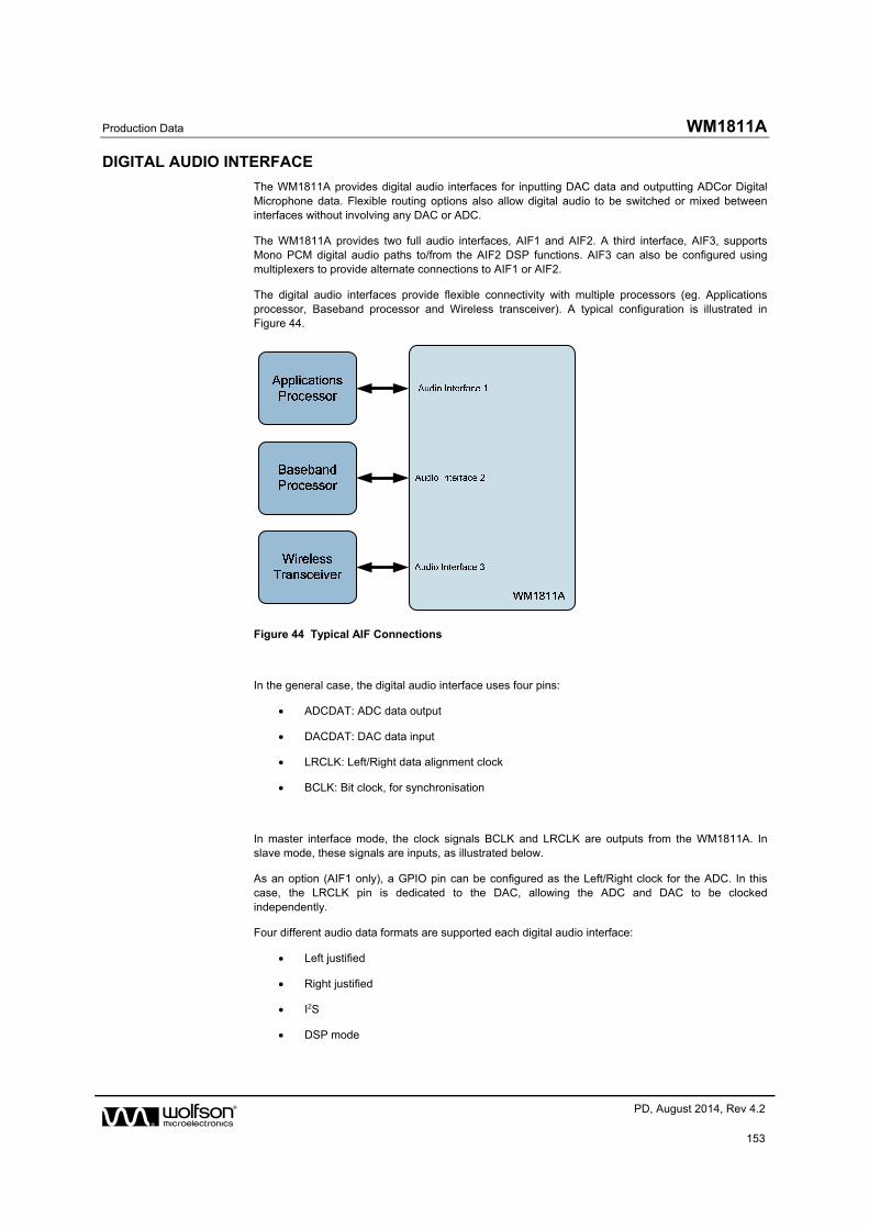
Production Data WM1811A
w PD, August 2014, Rev 4.2
153
DIGITAL AUDIO INTERFACE
The WM1811A provides digital audio interfaces for inputting DAC data and outputting ADCor Digital Microphone data. Flexible routing options also allow digital audio to be switched or mixed between interfaces without involving any DAC or ADC.
The WM1811A provides two full audio interfaces, AIF1 and AIF2. A third interface, AIF3, supports Mono PCM digital audio paths to/from the AIF2 DSP functions. AIF3 can also be configured using multiplexers to provide alternate connections to AIF1 or AIF2.
The digital audio interfaces provide flexible connectivity with multiple processors (eg. Applications processor, Baseband processor and Wireless transceiver). A typical configuration is illustrated in Figure 44.
Figure 44 Typical AIF Connections
In the general case, the digital audio interface uses four pins:
ADCDAT: ADC data output
DACDAT: DAC data input
LRCLK: Left/Right data alignment clock
BCLK: Bit clock, for synchronisation
In master interface mode, the clock signals BCLK and LRCLK are outputs from the WM1811A. In slave mode, these signals are inputs, as illustrated below.
As an option (AIF1 only), a GPIO pin can be configured as the Left/Right clock for the ADC. In this case, the LRCLK pin is dedicated to the DAC, allowing the ADC and DAC to be clocked independently.
Four different audio data formats are supported each digital audio interface:
Left justified
Right justified
I2S
DSP mode

WM1811A Production Data
w PD, August 2014, Rev 4.2
154
All four of these modes are MSB first. They are described inthe following sections. Refer to the “Signal Timing Requirements” section for timing information.
Time Division Multiplexing (TDM) is available in all four data format modes. The WM1811A can be configured to transmit and receive in one of two timeslots.
Two variants of DSP mode are supported - ‘Mode A’ and ‘Mode B’. Mono operation can be selected on either audio interface in both DSP modes. PCM operation is supported using the DSP mode.
MASTER AND SLAVE MODE OPERATION
The WM1811A digital audio interfaces can operate as a master or slave as shown in Figure 45 and Figure 46. The associated control bits are described in “Digital Audio Interface Control”.
Figure 45 Master Mode Figure 46 Slave Mode
OPERATION WITH TDM
Time division multiplexing (TDM) allows multiple devices to transfer data simultaneously on the same bus. The WM1811A ADCs and DACs support TDM in master and slave modes for all data formats and word lengths. TDM is enabled and configured using register bits defined in the “Digital Audio Interface Control” section.
WM1811A Processor
WM1811Aor similarCODEC ADCDAT
LRCLK
DACDAT
BCLK
ADCDAT
LRCLK
DACDAT
BCLK
WM1811A Processor
WM1811Aor similarCODEC ADCDAT
LRCLK
DACDAT
BCLK
ADCDAT
LRCLK
DACDAT
BCLK
Figure 47 TDM with WM1811A as Master Figure 48 TDM with Other CODEC as Master
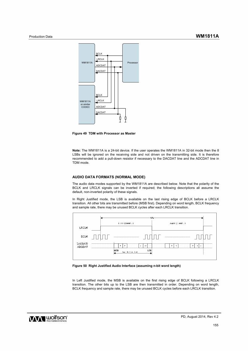
Production Data WM1811A
w PD, August 2014, Rev 4.2
155
WM1811A Processor
WM1811Aor similarCODEC ADCDAT
LRCLK
DACDAT
BCLK
ADCDAT
LRCLK
DACDAT
BCLK
Figure 49 TDM with Processor as Master
Note: The WM1811A is a 24-bit device. If the user operates the WM1811A in 32-bit mode then the 8 LSBs will be ignored on the receiving side and not driven on the transmitting side. It is therefore recommended to add a pull-down resistor if necessary to the DACDAT line and the ADCDAT line in TDM mode.
AUDIO DATA FORMATS (NORMAL MODE)
The audio data modes supported by the WM1811A are described below. Note that the polarity of the BCLK and LRCLK signals can be inverted if required; the following descriptions all assume the default, non-inverted polarity of these signals.
In Right Justified mode, the LSB is available on the last rising edge of BCLK before a LRCLK transition. All other bits are transmitted before (MSB first). Depending on word length, BCLK frequency and sample rate, there may be unused BCLK cycles after each LRCLK transition.
Figure 50 Right Justified Audio Interface (assuming n-bit word length)
In Left Justified mode, the MSB is available on the first rising edge of BCLK following a LRCLK transition. The other bits up to the LSB are then transmitted in order. Depending on word length, BCLK frequency and sample rate, there may be unused BCLK cycles before each LRCLK transition.

WM1811A Production Data
w PD, August 2014, Rev 4.2
156
Figure 51 Left Justified Audio Interface (assuming n-bit word length)
In I2S mode, the MSB is available on the second rising edge of BCLK following a LRCLK transition. The other bits up to the LSB are then transmitted in order. Depending on word length, BCLK frequency and sample rate, there may be unused BCLK cycles between the LSB of one sample and the MSB of the next.
Figure 52 I2S Justified Audio Interface (assuming n-bit word length)
In DSP mode, the left channel MSB is available on either the 1st (mode B) or 2nd (mode A) rising edge of BCLK following a rising edge of LRCLK. Right channel data immediately follows left channel data. Depending on word length, BCLK frequency and sample rate, there may be unused BCLK cycles between the LSB of the right channel data and the next sample.
The selected mode (Mode A or Mode B) is determined by the AIFnDAC_LRCLK_INV bits for the AIFn digital input (playback) signal paths, and by the AIFnADC_LRCLK_INV bits for the AIFn digital output (record) signal paths.
Note that the DSP Mode is selected independently for the input/output paths of each digital audio interface.
In device master mode, the LRCLKoutput will resemble the frame pulse shown in Figure 53 and Figure 54. In device slave mode, Figure 55 and Figure 56, it is possible to use any length of frame pulse less than 1/fs, providing the falling edge of the frame pulse occurs greater than one BCLK period before the rising edge of the next frame pulse.

Production Data WM1811A
w PD, August 2014, Rev 4.2
157
Figure 53 DSP Mode A (AIFnDAC_LRCLK_INV / AIFnADC_LRCLK_INV=0, Master)
Figure 54 DSP B Mode (AIFnDAC_LRCLK_INV / AIFnADC_LRCLK_INV=1, Master)
Figure 55 DSP Mode A(AIFnDAC_LRCLK_INV / AIFnADC_LRCLK_INV=0, Slave)
Figure 56 DSP Mode B (AIFnDAC_LRCLK_INV / AIFnADC_LRCLK_INV=1, Slave)
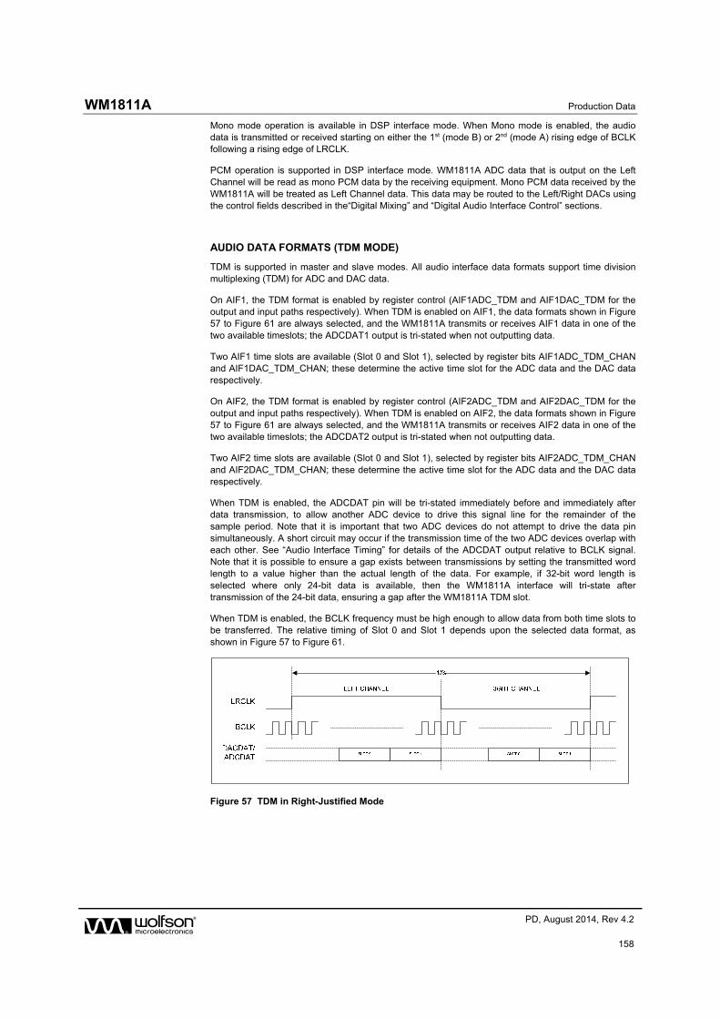
WM1811A Production Data
w PD, August 2014, Rev 4.2
158
Mono mode operation is available in DSP interface mode. When Mono mode is enabled, the audio data is transmitted or received starting on either the 1st (mode B) or 2nd (mode A) rising edge of BCLK following a rising edge of LRCLK.
PCM operation is supported in DSP interface mode. WM1811A ADC data that is output on the Left Channel will be read as mono PCM data by the receiving equipment. Mono PCM data received by the WM1811A will be treated as Left Channel data. This data may be routed to the Left/Right DACs using the control fields described in the“Digital Mixing” and “Digital Audio Interface Control” sections.
AUDIO DATA FORMATS (TDM MODE)
TDM is supported in master and slave modes. All audio interface data formats support time division multiplexing (TDM) for ADC and DAC data.
On AIF1, the TDM format is enabled by register control (AIF1ADC_TDM and AIF1DAC_TDM for the output and input paths respectively). When TDM is enabled on AIF1, the data formats shown in Figure 57 to Figure 61 are always selected, and the WM1811A transmits or receives AIF1 data in one of the two available timeslots; the ADCDAT1 output is tri-stated when not outputting data.
Two AIF1 time slots are available (Slot 0 and Slot 1), selected by register bits AIF1ADC_TDM_CHAN and AIF1DAC_TDM_CHAN; these determine the active time slot for the ADC data and the DAC data respectively.
On AIF2, the TDM format is enabled by register control (AIF2ADC_TDM and AIF2DAC_TDM for the output and input paths respectively). When TDM is enabled on AIF2, the data formats shown in Figure 57 to Figure 61 are always selected, and the WM1811A transmits or receives AIF2 data in one of the two available timeslots; the ADCDAT2 output is tri-stated when not outputting data.
Two AIF2 time slots are available (Slot 0 and Slot 1), selected by register bits AIF2ADC_TDM_CHAN and AIF2DAC_TDM_CHAN; these determine the active time slot for the ADC data and the DAC data respectively.
When TDM is enabled, the ADCDAT pin will be tri-stated immediately before and immediately after data transmission, to allow another ADC device to drive this signal line for the remainder of the sample period. Note that it is important that two ADC devices do not attempt to drive the data pin simultaneously. A short circuit may occur if the transmission time of the two ADC devices overlap with each other. See “Audio Interface Timing” for details of the ADCDAT output relative to BCLK signal. Note that it is possible to ensure a gap exists between transmissions by setting the transmitted word length to a value higher than the actual length of the data. For example, if 32-bit word length is selected where only 24-bit data is available, then the WM1811A interface will tri-state after transmission of the 24-bit data, ensuring a gap after the WM1811A TDM slot.
When TDM is enabled, the BCLK frequency must be high enough to allow data from both time slots to be transferred. The relative timing of Slot 0 and Slot 1 depends upon the selected data format, as shown in Figure 57 to Figure 61.
Figure 57 TDM in Right-Justified Mode

Production Data WM1811A
w PD, August 2014, Rev 4.2
159
Figure 58 TDM in Left-Justified Mode
Figure 59 TDM in I2S Mode
Figure 60 TDM in DSP Mode A
Figure 61 TDM in DSP Mode B
WM1811A Production Data
w PD, August 2014, Rev 4.2
160
DIGITAL AUDIO INTERFACE CONTROL
This section describes the configuration of the WM1811A digital audio interface paths.
Interfaces AIF1 and AIF2 can be configured as Master or Slave, or can be tri-stated. Each input and output signal path can be independently enabled or disabled. AIF output (digital record) and AIF input (digital playback) paths can use a common Left/Right clock, or can use separate clocks for mixed sample rates.
Interfaces AIF1 and AIF2 each support flexible formats, word-length, TDM configuration, channel swapping and input path digital boost functions. 8-bit companding modes and digital loopback is also possible.
A third interface, AIF3, supports Mono PCM digital audio paths to/from the AIF2 DSP functions. AIF3 can also be configured using multiplexers to provide alternate connections to AIF1 or AIF2. Note that AIF3 operates in Master mode only.
AIF1 - MASTER / SLAVE AND TRI-STATE CONTROL
The Digital Audio Interface AIF1 can operate in Master or Slave modes, selected by AIF1_MSTR. In Master mode, the BCLK1 and LRCLK1 signals are generated by the WM1811A when one or more AIF1 channels is enabled.
When AIF1_LRCLK_FRC or AIF1_CLK_FRC is set in Master mode, then LRCLK1 and ADCLRCLK1 are output at all times, including when none of the AIF1 audio channels is enabled. Note that LRCLK1 and ADCLRCLK1 are derived from BCLK1, and either an internal or external BCLK1 signal must also be present to generate LRCLK1 or ADCLRCLK1.
When AIF1_CLK_FRC is set in Master mode, then BCLK1is output at all times, including when none of the AIF1 audio channels is enabled.
The AIF1 interface can be tri-stated by setting the AIF1_TRI register. When this bit is set, then all of the AIF1 outputs are un-driven (high-impedance).Note that the ADCLRCLK1/GPIO1 pin is a configurable pin which may take different functions independent of AIF1. The AIF1_TRI register only controls the ADCLRCLK1/GPIO1 pin when its function is set to ADCLRCLK1. See “General Purpose Input/Output” to configure the GPIO1 pin.
REGISTER ADDRESS
BIT LABEL DEFAULT DESCRIPTION
R770 (0302h)
AIF1 Master/Slave
15 AIF1_TRI 0 AIF1 Audio Interface tri-state
0 = AIF1 pins operate normally
1 = Tri-state all AIF1 interface pins
Note that the GPIO1 pin is controlled by this register only when configured as ADCLRCLK1.
14 AIF1_MSTR 0 AIF1 Audio Interface Master Mode Select
0 = Slave mode
1 = Master mode
13 AIF1_CLK_FRC
0 Forces BCLK1, LRCLK1 and ADCLRCLK1 to be enabled when all AIF1 audio channels are disabled.
0 = Normal
1 = BCLK1, LRCLK1 and ADCLRCLK1 always enabled in Master mode
12 AIF1_LRCLK_FRC
0 Forces LRCLK1 and ADCLRCLK1 to be enabled when all AIF1 audio channels are disabled.
0 = Normal
1 = LRCLK1 and ADCLRCLK1 always enabled in Master mode
Table 85 AIF1 Master / Slave and Tri-state Control

Production Data WM1811A
w PD, August 2014, Rev 4.2
161
AIF1 - SIGNAL PATH ENABLE
The AIF1 interface supports two input channels and two output channels. Each of the available channels can be enabled or disabled using the register bits defined in Table 86. These register controls are illustrated in Figure 66.
REGISTER ADDRESS
BIT LABEL DEFAULT DESCRIPTION
R4 (0004h)
Power Management (4)
9 AIF1ADC1L_ENA
0 Enable AIF1ADC (Left) output path
0 = Disabled
1 = Enabled
8 AIF1ADC1R_ENA
0 Enable AIF1ADC (Right) output path
0 = Disabled
1 = Enabled
R5 (0005h)
Power Management (5)
9 AIF1DAC1L_ENA
0 Enable AIF1DAC (Left) input path
0 = Disabled
1 = Enabled
8 AIF1DAC1R_ENA
0 Enable AIF1DAC (Right) input path
0 = Disabled
1 = Enabled
Table 86 AIF1 Signal Path Enable
AIF1 - BCLK AND LRCLK CONTROL
The BCLK1 frequency is controlled relative to AIF1CLK by the AIF1_BCLK_DIV divider. See “Clocking and Sample Rates” for details of the AIF1 clock, AIF1CLK.
The LRCLK1 frequency is controlled relative to BCLK1 by the AIF1DAC_RATE divider.
In Master mode, the LRCLK1 output is generated by the WM1811A when any of the AIF1 channels is enabled. (Note that, when GPIO1 is configured as ADCLRCLK1, then only the AIF1 DAC channels will cause LRCLK1 to be output.)
In Slave mode, the LRCLK1 output is disabled by default to allow another digital audio interface to drive this pin. It is also possible to force the LRCLK1 signal to be output, using the AIF1DAC_LRCLK_DIR or AIF1ADC_LRCLK_DIR register bits, allowing mixed master and slave modes. (Note that, when GPIO1 is configured as ADCLRCLK1, then only the AIF1DAC_LRCLK_DIR bit will force the LRCLK1 signal.)
When the GPIO1 pin is configured as ADCLRCLK1, then the ADCLRCLK1 frequency is controlled relative to BCLK1 by the AIF1ADC_RATE divider. In this case, the ADCLRCLK1 is dedicated to AIF1 output, and the LRCLK1 pin is dedicated to AIF1 input, allowing different sample rates to be supported in the two paths.
In Master mode, with GPIO1 pin configured as ADCLRCLK1, this output is enabled when any of the AIF1 ADC channels is enabled. The ADCLRCLK1 signal can also be enabled in Slave mode, using the AIF1ADC_LRCLK_DIR bit, allowing mixed master and slave modes.
When the GPIO1 pin is not configured as ADCLRCLK1, then the LRCLK1 signal applies to the ADC and DAC channels, at a rate set by AIF1DAC_RATE.
See “General Purpose Input/Output” for the configuration of GPIO1.Note that, in Ultrasonic (4FS) mode, the GPIO1 pin must be configured as ADCLRCLK1.
The BCLK1 output can be inverted using the AIF1_BCLK_INV register bit. The LRCLK1 and ADCLRCLK1 output (when selected) can be inverted using the AIF1DAC_LRCLK_INV and AIF1ADC_LRCLK_INV register controls respectively.
Note that in Slave mode, when BCLK1 is an input, the AIF1_BCLK_INV register selects the polarity of the received BCLK1 signal. Under default conditions, DACDAT1 input is captured on the rising edge of BCLK1, as illustrated in Figure 4. When AIF1_BCLK_INV = 1, DACDAT1 input is captured on the falling edge of BCLK1.

WM1811A Production Data
w PD, August 2014, Rev 4.2
162
The AIF1 clock generators are controlled as illustrated in Figure 62.
Figure 62 Audio Interface 1 - BCLK and LRCLK Control
Production Data WM1811A
w PD, August 2014, Rev 4.2
163
REGISTER ADDRESS
BIT LABEL DEFAULT DESCRIPTION
R768 (0300h)
AIF1 Control (1)
8 AIF1_BCLK_INV
0 BCLK1 Invert
0 = BCLK1 not inverted
1 = BCLK1 inverted
Note that AIF1_BCLK_INV selects the BCLK1 polarity in Master mode and in Slave mode.
R771 (0303h)
AIF1 BCLK
8:4 AIF1_BCLK_DIV [4:0]
00100 BCLK1 Rate
00000 = AIF1CLK
00001 = AIF1CLK / 1.5
00010 = AIF1CLK / 2
00011 = AIF1CLK / 3
00100 = AIF1CLK / 4
00101 = AIF1CLK / 5
00110 = AIF1CLK / 6
00111 = AIF1CLK / 8
01000 = AIF1CLK / 11
01001 = AIF1CLK / 12
01010 = AIF1CLK / 16
01011 = AIF1CLK / 22
01100 = AIF1CLK / 24
01101 = AIF1CLK / 32
01110 = AIF1CLK / 44
01111 = AIF1CLK / 48
10000 = AIF1CLK / 64
10001 = AIF1CLK / 88
10010 = AIF1CLK / 96
10011 = AIF1CLK / 128
10100 = AIF1CLK / 176
10101 = AIF1CLK / 192
10110 - 11111 = Reserved
R772 (0304h)
AIF1ADC LRCLK
12 AIF1ADC_LRCLK_INV
0 Right, left and I2S modes – ADCLRCLK1 polarity
0 = normal ADCLRCLK1 polarity
1 = invert ADCLRCLK1 polarity
Note that AIF1ADC_LRCLK_INV selects the ADCLRCLK1 polarity in Master mode and in Slave mode.
DSP Mode – mode A/B select
0 = MSB is available on 2nd BCLK1 rising edge after ADCLRCLK1 rising edge (mode A)
1 = MSB is available on 1st BCLK1 rising edge after ADCLRCLK1 rising edge (mode B)
11 AIF1ADC_LRCLK_DIR
0 Allows ADCLRCLK1 to be enabled in Slave mode
0 = Normal
1 = ADCLRCLK1 enabled in Slave mode
10:0 AIF1ADC_RATE [10:0]
040h ADCLRCLK1 Rate
ADCLRCLK1 clock output = BCLK1 / AIF1ADC_RATE
Integer (LSB = 1)
Valid from 8..2047

WM1811A Production Data
w PD, August 2014, Rev 4.2
164
REGISTER ADDRESS
BIT LABEL DEFAULT DESCRIPTION
R773 (0305h)
AIF1DAC LRCLK
12 AIF1DAC_LRCLK_INV
0 Right, left and I2S modes – LRCLK1 polarity
0 = normal LRCLK1 polarity
1 = invert LRCLK1 polarity
Note that AIF1DAC_LRCLK_INV selects the LRCLK1 polarity in Master mode and in Slave mode.
DSP Mode – mode A/B select
0 = MSB is available on 2nd BCLK1 rising edge after LRCLK1 rising edge (mode A)
1 = MSB is available on 1st BCLK1 rising edge after LRCLK1 rising edge (mode B)
11 AIF1DAC_LRCLK_DIR
0 Allows LRCLK1 to be enabled in Slave mode
0 = Normal
1 = LRCLK1 enabled in Slave mode
10:0 AIF1DAC_RATE [10:0]
040h LRCLK1 Rate
LRCLK1 clock output = BCLK1 / AIF1DAC_RATE
Integer (LSB = 1)
Valid from 8..2047
Table 87 AIF1 BCLK and LRCLK Control
AIF1 - DIGITAL AUDIO DATA CONTROL
The register bits controlling the audio data format, word length, left/right channel selection and TDM control for AIF1 are described in Table 88.
When TDM mode is enabled on AIF1, the WM1811A can transmit and receive audio data in Slot 0 or Slot 1. In this case, the ADCDAT1 output is tri-stated during the unused timeslot, allowing another device to transmit data on the same pin. See “Signal Timing Requirements” for the associated timing details.(Note that, when TDM is not enabled on AIF1, the ADCDAT1 output is driven logic ‘0’ during the unused timeslot.)
In DSP mode, the left channel MSB is available on either the 1st (mode B) or 2nd (mode A) rising edge of BCLK following a rising edge of LRCLK (assuming default BCLK polarity).
When the AIF1DAC_LRCLK_INV bit is set in DSP mode, then DSP Mode B is selected for the AIF1 digital input (playback) signal path. When the AIF1DAC_LRCLK_INV bit is not set, then DSP Mode A is selected.
When the AIF1ADC_LRCLK_INV bit is set in DSP mode, then DSP Mode B is selected for the AIF1 digital output (record) signal path. When the AIF1ADC_LRCLK_INV bit is not set, then DSP Mode A is selected.
Note that the DSP Mode is selected independently for the input/output paths of each digital audio interface. Also note that the AIF1ADCLRCLK_INV bits remain valid even when the LRCLK signal is common for both paths. See Table 87 for details of the AIF1DAC_LRCLK_INV and AIF1ADC_LRCLK_INV register fields.
A digital gain function is available at the audio interface input path to boost the DAC volume when a small signal is received on DACDAT1. This is controlled using the AIF1DAC_BOOST register. To prevent clipping, this function should not be used when the boosted data is expected to be greater than 0dBFS.
REGISTER ADDRESS
BIT LABEL DEFAULT DESCRIPTION
R768 (0300h)
AIF1 Control (1)
15 AIF1ADCL_SRC
0 AIF1 Left Digital Audio interface source
0 = Left ADC data is output on left channel
1 = Right ADC data is output on left channel

Production Data WM1811A
w PD, August 2014, Rev 4.2
165
REGISTER ADDRESS
BIT LABEL DEFAULT DESCRIPTION
14 AIF1ADCR_SRC
1 AIF1 Right Digital Audio interface source
0 = Left ADC data is output on right channel
1 = Right ADC data is output on right channel
13 AIF1ADC_TDM
0 AIF1 transmit (ADC) TDM Enable
0 = Normal ADCDAT1 operation
1 = TDM enabled on ADCDAT1
12 AIF1ADC_TDM_CHAN
0 AIF1 transmit (ADC) TDM Slot Select
0 = Slot 0
1 = Slot 1
6:5 AIF1_WL [1:0]
10 AIF1 Digital Audio Interface Word Length
00 = 16 bits
01 = 20 bits
10 = 24 bits
11 = 32 bits
Note - 8-bit modes can be selected using the “Companding” control bits.
4:3 AIF1_FMT [1:0]
10 AIF1 Digital Audio Interface Format
00 = Right justified
01 = Left justified
10 = I2S Format
11 = DSP Mode
R769 (0301h)
AIF1 Control (2)
15 AIF1DACL_SRC
0 AIF1 Left Receive Data Source Select
0 = Left DAC receives left interface data
1 = Left DAC receives right interface data
14 AIF1DACR_SRC
1 AIF1 Right Receive Data Source Select
0 = Right DAC receives left interface data
1 = Right DAC receives right interface data
13 AIF1DAC_TDM
0 AIF1 receive (DAC) TDM Enable
0 = Normal DACDAT1 operation
1 = TDM enabled on DACDAT1
12 AIF1DAC_TDM_CHAN
0 AIF1 receive(DAC) TDM Slot Select
0 = Slot 0
1 = Slot 1
11:10 AIF1DAC_BOOST [1:0]
00 AIF1 Input Path Boost
00 = 0dB
01 = +6dB (input must not exceed -6dBFS)
10 = +12dB (input must not exceed -12dBFS)
11 = +18dB (input must not exceed -18dBFS)
R774 (0306h)
AIF1 DAC Data
1 AIF1DACL_DAT_INV
0 AIF1 Left Receive Data Invert
0 = Not inverted
1 = Inverted
0 AIF1DACR_DAT_INV
0 AIF1 Right Receive Data Invert
0 = Not inverted
1 = Inverted
R775 (0307h)
AIF1 ADC Data
1 AIF1ADCL_DAT_INV
0 AIF1 Left Transmit Data Invert
0 = Not inverted
1 = Inverted
0 AIF1ADCR_DAT_INV
0 AIF1 Right Transmit Data Invert
0 = Not inverted
1 = Inverted
Table 88 AIF1 Digital Audio Data Control

WM1811A Production Data
w PD, August 2014, Rev 4.2
166
AIF1 - MONO MODE
AIF1 can be configured to operate in mono DSP mode by setting AIF1_MONO = 1 as described in Table 89. Note that mono mode is only supported in DSP mode, ie when AIF1_FMT = 11.
In mono mode, the Left channel data or the Right channel data may be selected for output on ADCDAT1. The selected channel is determined by the AIF1ADC1L_ENA and AIF1ADC1R_ENA bits. (If both bits are set, then the Right channel data is selected.)
In mono mode, the DACDAT1 input can be enabled on the Left and/or Right signal paths using the AIF1DAC1L_ENA and AIF1DAC1R_ENA bits. The mono input can be enabled on both paths at the same time if required.
REGISTER ADDRESS
BIT LABEL DEFAULT DESCRIPTION
R769 (0301h)
AIF1 Control (2)
8 AIF1_MONO 0 AIF1 DSP Mono Mode
0 = Disabled
1 = Enabled
Note that Mono Mode is only supported when AIF1_FMT = 11.
Table 89 AIF1 Mono Mode Control
AIF1 - COMPANDING
The WM1811A supports A-law and -law companding on both transmit (ADC) and receive (DAC) sides of AIF1. This is configured using the register bits described inTable 90.
REGISTER ADDRESS
BIT LABEL DEFAULT DESCRIPTION
R769 (0301h)
AIF1 Control (2)
4 AIF1DAC_COMP
0 AIF1 Receive Companding Enable
0 = Disabled
1 = Enabled
3 AIF1DAC_COMPMODE
0 AIF1 Receive Companding Type
0 = µ-law
1 = A-law
2 AIF1ADC_COMP
0 AIF1 Transmit Companding Enable
0 = Disabled
1 = Enabled
1 AIF1ADC_COMPMODE
0 AIF1 Transmit Companding Type
0 = µ-law
1 = A-law
Table 90 AIF1 Companding
Companding involves using a piecewise linear approximation of the following equations (as set out by ITU-T G.711 standard) for data compression:
-law (where =255 for the U.S. and Japan):
F(x) = ln( 1 + |x|) / ln( 1 + ) for -1 ≤ x ≤ 1
A-law (where A=87.6 for Europe):
F(x) = A|x| / ( 1 + lnA) for x ≤ 1/A
F(x) = ( 1 + lnA|x|) / (1 + lnA) for 1/A ≤ x ≤ 1
The companded data is also inverted as recommended by the G.711 standard (all 8 bits are inverted for -law, all even data bits are inverted for A-law). The data will be transmitted as the first 8 MSBs of data.

Production Data WM1811A
w PD, August 2014, Rev 4.2
167
Companding converts 13 bits (-law) or 12 bits (A-law) to 8 bits using non-linear quantization. This provides greater precision for low amplitude signals than for high amplitude signals, resulting in a greater usable dynamic range than 8 bit linear quantization. The companded signal is an 8-bit word comprising sign (1 bit), exponent (3 bits) and mantissa (4 bits).
AIF1 8-bit mode is selected whenever AIF1DAC_COMP=1 or AIF1ADC_COMP=1. The use of 8-bit data allows samples to be passed using as few as 8 BCLK1 cycles per LRCLK1 frame. When using DSP mode B, 8-bit data words may be transferred consecutively every 8 BCLK1 cycles.
AIF1 8-bit mode (without Companding) may be enabled by setting AIF1DAC_COMPMODE=1 or AIF1ADC_COMPMODE=1, when AIF1DAC_COMP=0 and AIF1ADC_COMP=0.
BIT7 BIT[6:4] BIT[3:0]
SIGN EXPONENT MANTISSA
Table 91 8-bit Companded Word Composition
u-law Companding
0
20
40
60
80
100
120
0 0.1 0.2 0.3 0.4 0.5 0.6 0.7 0.8 0.9 1
Normalised Input
Co
mp
and
ed O
utp
ut
0
0.1
0.2
0.3
0.4
0.5
0.6
0.7
0.8
0.9
1
No
rmal
ised
Ou
tpu
t
Figure 63 µ-Law Companding
A-law Companding
0
20
40
60
80
100
120
0 0.2 0.4 0.6 0.8 1
Normalised Input
Co
mp
and
ed O
utp
ut
0
0.1
0.2
0.3
0.4
0.5
0.6
0.7
0.8
0.9
1
No
rmal
ised
Ou
tpu
t
Figure 64 A-Law Companding

WM1811A Production Data
w PD, August 2014, Rev 4.2
168
AIF1 - LOOPBACK
The AIF1 interface can provide a Loopback option. When the AIF1_LOOPBACK bit is set, then AIF1 digital audio output is routed to the AIF1 digital audio input. The normal input (DACDAT1) is not used when AIF1 Loopback is enabled.
REGISTER ADDRESS
BIT LABEL DEFAULT DESCRIPTION
R769 (0301h)
AIF1 Control (2)
0 AIF1_LOOPBACK
0 AIF1 Digital Loopback Function
0 = No loopback
1 = Loopback enabled (ADCDAT1 data output is directly input to DACDAT1 data input).
Table 92 AIF1 Loopback
AIF1 - DIGITAL PULL-UP AND PULL-DOWN
The WM1811A provides integrated pull-up and pull-down resistors on each of the DACDAT1, LRCLK1 and BCLK1 pins. This provides a flexible capability for interfacing with other devices.
Each of the pull-up and pull-down resistors can be configured independently using the register bits described in Table 93. Note that if the Pull-up and Pull-down are both enabled for any pin, then the pull-up and pull-down will be disabled.
REGISTER ADDRESS
BIT LABEL DEFAULT DESCRIPTION
R1824 (0720h)
Pull Control (1)
5 DACDAT1_PU 0 DACDAT1 Pull-up enable
0 = Disabled
1 = Enabled
4 DACDAT1_PD 0 DACDAT1 Pull-down enable
0 = Disabled
1 = Enabled
3 DACLRCLK1_PU
0 LRCLK1 Pull-up enable
0 = Disabled
1 = Enabled
2 DACLRCLK1_PD
0 LRCLK1 Pull-down enable
0 = Disabled
1 = Enabled
1 BCLK1_PU 0 BCLK1 Pull-up enable
0 = Disabled
1 = Enabled
0 BCLK1_PD 0 BCLK1 Pull-down enable
0 = Disabled
1 = Enabled
Table 93 AIF1 Digital Pull-Up and Pull-Down Control
AIF2 - MASTER / SLAVE AND TRI-STATE CONTROL
The Digital Audio Interface AIF2 can operate in Master or Slave modes, selected by AIF2_MSTR. In Master mode, the BCLK2 and LRCLK2 signals are generated by the WM1811A when one or more AIF2 channels is enabled.
When AIF2_LRCLK_FRC or AIF2_CLK_FRC is set in Master mode, then LRCLK2 is output at all times, including when none of the AIF2 audio channels is enabled. Note that LRCLK2 is derived from BCLK2, and either an internal or external BCLK2 signal must be present to generate LRCLK2.
When AIF2_CLK_FRC is set in Master mode, then BCLK2 is output at all times, including when none of the AIF2 audio channels is enabled.

Production Data WM1811A
w PD, August 2014, Rev 4.2
169
The AIF2 interface can be tri-stated by setting the AIF2_TRI register. When this bit is set, then all of the AIF2 outputs are un-driven (high-impedance).The AIF2_TRI register only affects those pins which are configured for AIF2 functions; it does not affect pins which are configured for other functions.
REGISTER ADDRESS
BIT LABEL DEFAULT DESCRIPTION
R786 (0312h)
AIF2 Master/Slave
15 AIF2_TRI 0 AIF2 Audio Interface tri-state
0 = AIF2 pins operate normally
1 = Tri-state all AIF2 interface pins
Note that pins not configured as AIF2 functions are not affected by this register.
14 AIF2_MSTR 0 AIF2 Audio Interface Master Mode Select
0 = Slave mode
1 = Master mode
13 AIF2_CLK_FRC
0 Forces BCLK2 and LRCLK2to be enabled when all AIF2 audio channels are disabled.
0 = Normal
1 = BCLK2 and LRCLK2always enabled in Master mode
12 AIF2_LRCLK_FRC
0 Forces LRCLK2 to be enabled when all AIF2 audio channels are disabled.
0 = Normal
1 = LRCLK2 always enabled in Master mode
Table 94 AIF2 Master / Slave and Tri-state Control
AIF2 - SIGNAL PATH ENABLE
The AIF2 interface supports two input channels and two output channels. Each of the available channels can be enabled or disabled using the register bits defined in Table 95.These register controls are illustrated in Figure 66.
REGISTER ADDRESS
BIT LABEL DEFAULT DESCRIPTION
R4 (0004h)
Power Management (4)
13 AIF2ADCL_ENA
0 Enable AIF2ADC (Left) output path
0 = Disabled
1 = Enabled
This bit must be set for AIF2 or AIF3 output of the AIF2ADC (Left) signal.
12 AIF2ADCR_ENA
0 Enable AIF2ADC (Right) output path
0 = Disabled
1 = Enabled
This bit must be set for AIF2 or AIF3 output of the AIF2ADC (Left) signal.
R5 (0005h)
Power Management (5)
13 AIF2DACL_ENA
0 Enable AIF2DAC (Left) input path
0 = Disabled
1 = Enabled
12 AIF2DACR_ENA
0 Enable AIF2DAC (Right) input path
0 = Disabled
1 = Enabled
R792 (0318h)
AIF2 Tx Control
1 AIF2TXL_ENA
1 Enable AIF2DAC (Left) input path
0 = Disabled
1 = Enabled
This bit must be set for AIF2 output of the AIF2ADC (Left) signal. For AIF3 output only, this bit can be set to 0.

WM1811A Production Data
w PD, August 2014, Rev 4.2
170
REGISTER ADDRESS
BIT LABEL DEFAULT DESCRIPTION
0 AIF2TXR_ENA
1 Enable AIF2DAC (Right) input path
0 = Disabled
1 = Enabled
This bit must be set for AIF2 output of the AIF2ADC (Left) signal. For AIF3 output only, this bit can be set to 0.
Table 95 AIF2 Signal Path Enable
AIF2 - BCLK AND LRCLK CONTROL
The BCLK2 frequency is controlled relative to AIF2CLK by the AIF2_BCLK_DIV divider. See “Clocking and Sample Rates” for details of the AIF2 clock, AIF2CLK.
The LRCLK2 frequency is controlled relative to BCLK2 by the AIF2DAC_RATE divider.Note that the LRCLK2 signal is shared by the AIF2 input and AIF2 output paths; accordingly, the AIF2 input and AIF2 output must always operate at the same sample rate.
In Master mode, the LRCLK2 output is generated by the WM1811A when any of the AIF2 channels is enabled.
In Slave mode, the LRCLK2 output is disabled by default to allow another digital audio interface to drive this pin. It is also possible to force the LRCLK2 signal to be output, using the AIF2DAC_LRCLK_DIR register bit, allowing mixed master and slave modes.
The BCLK2 and LRCLK2 output can be inverted using the AIF2_BCLK_INV and AIF2DAC_LRCLK_INV register bits respectively.
Note that in Slave mode, when BCLK2 is an input, the AIF2_BCLK_INV register selects the polarity of the received BCLK2 signal. Under default conditions, DACDAT2 input is captured on the rising edge of BCLK2, as illustrated in Figure 4. When AIF2_BCLK_INV = 1, DACDAT2 input is captured on the falling edge of BCLK2.
The AIF2 clock generators are controlled as illustrated in Figure 65.
Figure 65 Audio Interface 2 - BCLK and LRCLK Control

Production Data WM1811A
w PD, August 2014, Rev 4.2
171
REGISTER ADDRESS
BIT LABEL DEFAULT DESCRIPTION
R784 (0310h)
AIF2 Control (1)
8 AIF2_BCLK_INV
0 BCLK2 Invert
0 = BCLK2 not inverted
1 = BCLK2 inverted
Note that AIF2_BCLK_INV selects the BCLK2 polarity in Master mode and in Slave mode.
R787 (0313h)
AIF2 BCLK
8:4 AIF2_BCLK_DIV [4:0]
00100 BCLK2 Rate 00000 = AIF2CLK 00001 = AIF2CLK / 1.5 00010 = AIF2CLK / 2 00011 = AIF2CLK / 3 00100 = AIF2CLK / 4 00101 = AIF2CLK / 5 00110 = AIF2CLK / 6 00111 = AIF2CLK / 8 01000 = AIF2CLK / 11 01001 = AIF2CLK / 12 01010 = AIF2CLK / 16 01011 = AIF2CLK / 22 01100 = AIF2CLK / 24 01101 = AIF2CLK / 32 01110 = AIF2CLK / 44 01111 = AIF2CLK / 48 10000 = AIF2CLK / 64 10001 = AIF2CLK / 88 10010 = AIF2CLK / 96 10011 = AIF2CLK / 128 10100 = AIF2CLK / 176 10101 = AIF2CLK / 192 10110 - 11111 = Reserved
R789 (0315h)
AIF2DAC LRCLK
12 AIF2DAC_LRCLK_INV
0 Right, left and I2S modes – LRCLK2 polarity
0 = normal LRCLK2 polarity
1 = invert LRCLK2 polarity
Note that AIF2DAC_LRCLK_INV selects the LRCLK2 polarity in Master mode and in Slave mode.
DSP Mode – mode A/B select (AIF2 input)
0 = MSB is available on 2nd BCLK2 rising edge after LRCLK2 rising edge (mode A)
1 = MSB is available on 1st BCLK2 rising edge after LRCLK2 rising edge (mode B)
11 AIF2DAC_LRCLK_DIR
0 Allows LRCLK2 to be enabled in Slave mode
0 = Normal
1 = LRCLK2 enabled in Slave mode
10:0 AIF2DAC_RATE [10:0]
040h LRCLK2 Rate
LRCLK2 clock output = BCLK2 / AIF2DAC_RATE
Integer (LSB = 1)
Valid from 8..2047
Table 96 AIF2 BCLK and LRCLK Control

WM1811A Production Data
w PD, August 2014, Rev 4.2
172
AIF2 - DIGITAL AUDIO DATA CONTROL
The register bits controlling the audio data format, word length, left/right channel selection and TDM control for AIF2 are described in Table 97.
When TDM mode is enabled on AIF2, the WM1811A can transmit and receive audio data in Slot 0 or Slot 1. In this case, the ADCDAT2 output is tri-stated during the unused timeslot, allowing another device to transmit data on the same pin. See “Signal Timing Requirements” for the associated timing details.(Note that, when TDM is not enabled on AIF2, the ADCDAT2 output is driven logic ‘0’ during the unused timeslot.)
In DSP mode, the left channel MSB is available on either the 1st (mode B) or 2nd (mode A) rising edge of BCLK following a rising edge of LRCLK (assuming default BCLK polarity).
When the AIF2DAC_LRCLK_INV bit is set in DSP mode, then DSP Mode B is selected for the AIF2 digital input (playback) signal path. When the AIF2DAC_LRCLK_INV bit is not set, then DSP Mode A is selected.
When the AIF2ADC_LRCLK_INV bit is set in DSP mode, then DSP Mode B is selected for the AIF2 digital output (record) signal path. When the AIF2ADC_LRCLK_INV bit is not set, then DSP Mode A is selected.
Note that the DSP Mode is selected independently for the input/output paths of each digital audio interface. The LRCLK signal is common for both paths so, for typical applications, the AIF2DAC_LRCLK_INV and AIF2ADC_LRCLK_INV bits should be set to the same value. The AIF2DAC_LRCLK_INV bit is defined in Table 96.
A digital gain function is available at the audio interface input path to boost the DAC volume when a small signal is received on DACDAT2. This is controlled using the AIF2DAC_BOOST register. To prevent clipping, this function should not be used when the boosted data is expected to be greater than 0dBFS.
REGISTER ADDRESS
BIT LABEL DEFAULT DESCRIPTION
R784 (0310h)
AIF2 Control (1)
15 AIF2ADCL_SRC
0 AIF2 Left Digital Audio interface source
0 = Left ADC data is output on left channel
1 = Right ADC data is output on left channel
14 AIF2ADCR_SRC
1 AIF2 Right Digital Audio interface source
0 = Left ADC data is output on right channel
1 = Right ADC data is output on right channel
13 AIF2ADC_TDM
0 AIF2 transmit (ADC) TDM Enable
0 = Normal ADCDAT2 operation
1 = TDM enabled on ADCDAT2
12 AIF2ADC_TDM_CHAN
0 AIF2 transmit (ADC) TDM Slot Select
0 = Slot 0
1 = Slot 1
6:5 AIF2_WL [1:0]
10 AIF2 Digital Audio Interface Word Length
00 = 16 bits
01 = 20 bits
10 = 24 bits
11 = 32 bits
Note - 8-bit modes can be selected using the “Companding” control bits.
4:3 AIF2_FMT [1:0]
10 AIF2 Digital Audio Interface Format
00 = Right justified
01 = Left justified
10 = I2S Format
11 = DSP Mode
R785 (0311h)
AIF2 Control (2)
15 AIF2DACL_SRC
0 AIF2 Left Receive Data Source Select
0 = Left DAC receives left interface data
1 = Left DAC receives right interface data

Production Data WM1811A
w PD, August 2014, Rev 4.2
173
REGISTER ADDRESS
BIT LABEL DEFAULT DESCRIPTION
14 AIF2DACR_SRC
1 AIF2 Right Receive Data Source Select
0 = Right DAC receives left interface data
1 = Right DAC receives right interface data
13 AIF2DAC_TDM
0 AIF2 receive (DAC) TDM Enable
0 = Normal DACDAT2 operation
1 = TDM enabled on DACDAT2
12 AIF2DAC_TDM_CHAN
0 AIF2 receive(DAC) TDM Slot Select
0 = Slot 0
1 = Slot 1
11:10 AIF2DAC_BOOST [1:0]
00 AIF2 Input Path Boost
00 = 0dB
01 = +6dB (input must not exceed -6dBFS)
10 = +12dB (input must not exceed -12dBFS)
11 = +18dB (input must not exceed -18dBFS)
R788 (0314h)
AIF2ADC LRCLK
12 AIF2ADC_LRCLK_INV
0 DSP Mode – mode A/B select (AIF2 output)
0 = MSB is available on 2nd BCLK2 rising edge after LRCLK2 rising edge (mode A)
1 = MSB is available on 1st BCLK2 rising edge after LRCLK2 rising edge (mode B)
R790 (0316h)
AIF2 DAC Data
1 AIF2DACL_DAT_INV
0 AIF2 Left Receive Data Invert
0 = Not inverted
1 = Inverted
0 AIF2DACR_DAT_INV
0 AIF2 Right Receive Data Invert
0 = Not inverted
1 = Inverted
R791 (0317h)
AIF2 ADC Data
1 AIF2ADCL_DAT_INV
0 AIF2 Left Transmit Data Invert
0 = Not inverted
1 = Inverted
0 AIF2ADCR_DAT_INV
0 AIF2 Right Transmit Data Invert
0 = Not inverted
1 = Inverted
Table 97 AIF2 Digital Audio Data Control
AIF2 - MONO MODE
AIF2 can be configured to operate in mono DSP mode by setting AIF2_MONO = 1 as described in Table 98. Note that mono mode is only supported in DSP mode, ie when AIF2_FMT = 11.
In mono mode, the Left channel data or the Right channel data may be selected for output on ADCDAT2. The selected channel is determined by the AIF2ADCL_ENA and AIF2ADCR_ENA bits. (If both bits are set, then the Right channel data is selected.)
In mono mode, the DACDAT2 input can be enabled on the Left and/or Right signal paths using the AIF2DACL_ENA and AIF2DACR_ENA bits. The mono input can be enabled on both paths at the same time if required.
REGISTER ADDRESS
BIT LABEL DEFAULT DESCRIPTION
R785 (0311h)
AIF2 Control (2)
8 AIF2_MONO 0 AIF2 DSP Mono Mode
0 = Disabled
1 = Enabled
Note that Mono Mode is only supported when AIF2_FMT = 11.
Table 98 AIF2 Mono Mode Control

WM1811A Production Data
w PD, August 2014, Rev 4.2
174
AIF2 - COMPANDING
The WM1811A supports A-law and -law companding on both transmit (ADC) and receive (DAC) sides of AIF2. This is configured using the register bits described in Table 99.
For more details on Companding, see the Audio Interface AIF1 description above.
REGISTER ADDRESS
BIT LABEL DEFAULT DESCRIPTION
R785 (0311h)
AIF2 Control (2)
4 AIF2DAC_COMP
0 AIF2 Receive Companding Enable
0 = Disabled
1 = Enabled
3 AIF2DAC_COMPMODE
0 AIF2 Receive Companding Type
0 = µ-law
1 = A-law
2 AIF2ADC_COMP
0 AIF2 Transmit Companding Enable
0 = Disabled
1 = Enabled
1 AIF2ADC_COMPMODE
0 AIF2 Transmit Companding Type
0 = µ-law
1 = A-law
Table 99 AIF2 Companding
AIF2 - LOOPBACK
The AIF2 interface can provide a Loopback option. When the AIF2_LOOPBACK bit is set, then AIF2 digital audio output is routed to the AIF2 digital audio input. The normal input (DACDAT2) is not used when AIF2 Loopback is enabled.
REGISTER ADDRESS
BIT LABEL DEFAULT DESCRIPTION
R785 (0311h)
AIF2 Control (2)
0 AIF2_LOOPBACK
0 AIF2 Digital Loopback Function
0 = No loopback
1 = Loopback enabled (ADCDAT2 data output is directly input to DACDAT2 data input).
Table 100 AIF2 Loopback

Production Data WM1811A
w PD, August 2014, Rev 4.2
175
AIF2 - DIGITAL PULL-UP AND PULL-DOWN
The WM1811A provides integrated pull-up and pull-down resistors on each of the DACDAT2, DACLRCLK2 and BCLK2 pins. This provides a flexible capability for interfacing with other devices.
Each of the pull-up and pull-down resistors can be configured independently using the register bits described inTable 101.Note that if the Pull-up and Pull-down are both enabled for any pin, then the pull-up and pull-down will be disabled.
REGISTER ADDRESS
BIT LABEL DEFAULT DESCRIPTION
R1794 (0702h)
Pull Control (BCLK2)
14 BCLK2_PU 0 BCLK2Pull-up enable
0 = Disabled
1 = Enabled
13 BCLK2_PD 1 BCLK2 Pull-down enable
0 = Disabled
1 = Enabled
R1795 (0703h)
Pull Control (DACLRCLK2)
14 DACLRCLK2_PU
0 DACLRCLK2Pull-up enable
0 = Disabled
1 = Enabled
13 DACLRCLK2_PD
1 DACLRCLK2Pull-down enable
0 = Disabled
1 = Enabled
R1796 (0704h)
Pull Control (DACDAT2)
14 DACDAT2_PU 0 DACDAT2Pull-up enable
0 = Disabled
1 = Enabled
13 DACDAT2_PD 1 DACDAT2Pull-down enable
0 = Disabled
1 = Enabled
Table 101 AIF2 Digital Pull-Up and Pull-Down Control

WM1811A Production Data
w PD, August 2014, Rev 4.2
176
AIF3 - SIGNAL PATH CONFIGURATION AND TRI-STATE CONTROL
The AIF3 interface provides Mono PCM digital audio paths to/from the AIF2 DSP functions. The AIF3 interface can also support stereo digital audio paths via multiplexers to provide alternate connections to AIF1 or AIF2.The relevant multiplexers are illustrated in Figure 66.
AIF1_DACDAT_SRC
AIF3_ADCDAT_SRC[1:0]
AIF2_ADCDAT_SRC
DIGITAL AUDIOINTERFACE 2 (AIF2)
DIGITAL AUDIOINTERFACE 1 (AIF1)
MONO PCM INTERFACE
Left / Right source select / Mono Mix control
AIF2DAC_SRC
AIF3ADC_SRC[1:0]
AIF2_DACDAT_SRC
Left / Right source select / Mono Mix control
Figure 66 Audio Interface AIF3 Configuration
Note that all of the AIF3 connections are supported on pins which also provide GPIO functions. These pins must be configured as AIF functions when used as audio interface pins. See “General Purpose Input/Output”.
The GPIO8 pin supports the DACDAT3 function, which provides the input to the AIF3 Mono PCM interface.
When AIF3 Mono PCM input is used, this must be configured as an input to the AIF2 input paths using the AIF2DAC_SRC register as described in Table 102. The AIF3 Mono input may be selected on either channel (Left or Right), with AIF2 input enabled on the opposite channel at the same time.
When AIF3 Mono PCM input is used, the AIF2 input paths must be enabled using the AIF2DACR_ENA and AIF2DACL_ENA register bits defined in Table 95.
The DACDAT3 input pin can also be used as an input (mono or stereo) to AIF1 or AIF2. The data input source for AIF1 is selected using the AIF1_DACDAT_SRC register. The data input source for AIF2 is selected using the AIF2_DACDAT_SRC register.
The DACDAT3 input pin can also be routed to the ADCDAT2 output. The ADCDAT2 source is selected using the AIF2_ADCDAT_SRC register.

Production Data WM1811A
w PD, August 2014, Rev 4.2
177
The GPIO9 pin supports the ADCDAT3 function, which supports the output from the AIF3 Mono PCM interface.The source for the ADCDAT3 pin is selected using the AIF3_ADCDAT_SRC register.
When AIF3 Mono PCM output is used, the data source must be configured using the AIF3ADC_SRC register; this selects either the Left or Right AIF2 output paths as the data source.
When AIF3 Mono PCM output is used, the AIF2 output paths must be enabled using the AIF2ADCR_ENA and AIF2ADCL_ENA register bits. Note that, if AIF3 Mono PCM output is required and AIF2 output is not used, then the AIF2 output can be disabled using the AIF2TXL_ENA and AIF2TXR_ENA registers.See Table 95 for details of these registers.
The ADCDAT3 pin can also be used as an alternate data output (mono or stereo) from AIF1 or AIF2, or can be connected to the DACDAT2 data input.
The AIF3 interface can be tri-stated by setting the AIF3_TRI register. When this bit is set, then all of the AIF3 outputs are un-driven (high-impedance). The AIF3_TRI register only affects those pins which are configured for AIF3 functions; it does not affect pins which are configured for other functions.
The AIF3 control registers are described in Table 102.
REGISTER ADDRESS
BIT LABEL DEFAULT DESCRIPTION
R6 (0006h)
Power Management (6)
10:9 AIF3ADC_SRC [1:0]
00 AIF3 Mono PCM output source select
00 = None
01 = AIF2ADC (Left) output path
10 = AIF2ADC (Right) output path
11 = Reserved
8:7 AIF2DAC_SRC [1:0]
00 AIF2 input path select
00 = Left and Right inputs from AIF2
01 = Left input from AIF2; Right input from AIF3
10 = Left input from AIF3; Right input from AIF2
11 = Reserved
5 AIF3_TRI 0 AIF3 Audio Interface tri-state
0 = AIF3 pins operate normally
1 = Tri-state all AIF3 interface pins
Note that pins not configured as AIF3 functions are not affected by this register.
4:3 AIF3_ADCDAT_SRC [1:0]
00 GPIO9/ADCDAT3 Source select
00 = AIF1 ADCDAT1
01 = AIF2 ADCDAT2
10 = DACDAT2
11 = AIF3 Mono PCM output
Note that GPIO9 must be configured as ADCDAT3.
2 AIF2_ADCDAT_SRC
0 ADCDAT2 Source select
0 = AIF2 ADCDAT2
1 = GPIO8/DACDAT3
For selection 1, the GPIO8 pin must also be configured as DACDAT3.
1 AIF2_DACDAT_SRC
0 AIF2 DACDAT Source select
0 = DACDAT2
1 = GPIO8/DACDAT3
For selection 1, the GPIO8 pin must also be configured as DACDAT3.

WM1811A Production Data
w PD, August 2014, Rev 4.2
178
REGISTER ADDRESS
BIT LABEL DEFAULT DESCRIPTION
0 AIF1_DACDAT_SRC
0 AIF1 DACDAT Source select
0 = DACDAT1
1 = GPIO8/DACDAT3
Note that, for selection 1, the GPIO8 pin must be configured as DACDAT3.
Table 102 AIF3 Signal Path Configuration
AIF3 - BCLK AND LRCLK CONTROL
The GPIO10 pin supports the LRCLK3 function. When configured as LRCLK3, this pin outputs the LRCLK signal from AIF1 or AIF2. The applicable AIF source is determined automatically as defined in Table 103. Note that the LRCLK3 signal is also controlled by the logic illustrated in Figure 62 (AIF1) or Figure 65 (AIF2), depending on the selected AIF source.
The GPIO11 pin supports the BCLK3 function. When configured as BCLK3, this pin outputs the BCLK signal from AIF1 or AIF2. The applicable AIF source is determined automatically as defined in Table 103. Note that the BCLK3 signal is also controlled by the logic illustrated in Figure 62 (AIF1) or Figure 65 (AIF2), depending on the selected AIF source.
CONDITION DESCRIPTION
AIF1_DACDAT_SRC = 1
(DACDAT3 selected as AIF1 data input)
or
AIF3_ADCDAT_SRC[1:0] = 00
(AIF1 data output selected on ADCDAT3)
AIF1 selected as BCLK3 / LRCLK3 source
All other conditions
AIF2 selected as BCLK3 / LRCLK3 source
Table 103 BCLK3 / LRCLK3 Configuration
The LRCLK3 output can be inverted by setting the AIF3_LRCLK_INV register. Note that AIF3 operates in Master mode only.
REGISTER ADDRESS
BIT LABEL DEFAULT DESCRIPTION
R800 (0320h)
AIF3 Control (1)
7 AIF3_LRCLK_INV
0 Right, left and I2S modes – LRCLK3 polarity
0 = normal LRCLK3 polarity
1 = invert LRCLK3 polarity
DSP Mode – mode A/B select
0 = MSB is available on 2nd BCLK3 rising edge after LRCLK3 rising edge (mode A)
1 = MSB is available on 1st BCLK3 rising edge after LRCLK3 rising edge (mode B)
Table 104 AIF3 LRCLK Control

Production Data WM1811A
w PD, August 2014, Rev 4.2
179
AIF3 - DIGITAL AUDIO DATA CONTROL
The register bits controlling the AIF3Mono PCM interface are described in Table 105.
Note that these registers control the AIF3 Mono PCM interface only; they are not applicable to the ADCDAT3 and DACDAT3 signal paths when these pins are selected as alternate inputs to the AIF1 or AIF2 interfaces.
The audio data format for AIF3 is set the same as AIF2; this is controlled using the AIF2_FMT register, as described in see Table 97.
In DSP mode, the AIF3 Mono channel MSB is available on either the 1st (mode B) or 2nd (mode A) rising edge of BCLK following a rising edge of LRCLK. The applicable DSP mode is selected using the AIF3_LRCLK_INV bit, as described in Table 104.
In Left justified, Right justified and I2S modes, the AIF3 Mono interface data is transmitted and received in the Left channel data bits of the ADCDAT3 and DACDAT3 channels.
A digital gain function is available at the audio interface input path to boost the DAC volume when a small signal is received on DACDAT3. This is controlled using the AIF3DAC_BOOST register. To prevent clipping, this function should not be used when the boosted data is expected to be greater than 0dBFS.
REGISTER ADDRESS
BIT LABEL DEFAULT DESCRIPTION
R800 (0320h)
AIF3 Control (1)
6:5 AIF3_WL [1:0]
10 AIF3 Digital Audio Interface Word Length
00 = 16 bits
01 = 20 bits
10 = 24 bits
11 = 32 bits
Note - 8-bit modes can be selected using the “Companding” control bits.
Note that this controls the AIF3 Mono PCM interface path only; it does not affect AIF3 inputs/outputs routed to AIF1 or AIF2.
R801 (0321h)
AIF3 Control (2)
11:10 AIF3DAC_BOOST [1:0]
00 AIF3 Input Path Boost
00 = 0dB
01 = +6dB (input must not exceed -6dBFS)
10 = +12dB (input must not exceed -12dBFS)
11 = +18dB (input must not exceed -18dBFS)
Note that this controls the AIF3 Mono PCM interface path only; it does not affect DACDAT3 input to AIF1 or AIF2.
R802 (0322h)
AIF3DAC Data
0 AIF3DAC_DAT_INV
0 AIF3 Receive Data Invert
0 = Not inverted
1 = Inverted
Note that this controls the AIF3 Mono PCM interface path only; it does not affect DACDAT3 input to AIF1 or AIF2.
R803 (0323h)
AIF3ADC Data
0 AIF3ADC_DAT_INV
0 AIF3 Transmit Data Invert
0 = Not inverted
1 = Inverted
Note that this controls the AIF3 Mono PCM interface path only; it does not affect ADCDAT3 output from AIF1 or AIF2.
Table 105 AIF3 Digital Audio Data Control

WM1811A Production Data
w PD, August 2014, Rev 4.2
180
AIF3 - COMPANDING
The WM1811A supports A-law and -law companding on both transmit (ADC) and receive (DAC) sides of AIF3. This is configured using the register bits described in Table 106.
Note that these registers control the AIF3 Mono PCM interface only; they are not applicable to the ADCDAT3 and DACDAT3 signal paths when these pins are selected as alternate inputs to the AIF1 or AIF2 interfaces.
For more details on Companding, see the Audio Interface AIF1 description above.
REGISTER ADDRESS
BIT LABEL DEFAULT DESCRIPTION
R801 (0321h)
AIF3 Control (2)
4 AIF3DAC_COMP
0 AIF3 Receive Companding Enable
0 = Disabled
1 = Enabled
Note that this controls the AIF3 Mono PCM interface path only; it does not affect DACDAT3 input to AIF1 or AIF2.
3 AIF3DAC_COMPMODE
0 AIF3 Receive Companding Type
0 = µ-law
1 = A-law
Note that this controls the AIF3 Mono PCM interface path only; it does not affect DACDAT3 input to AIF1 or AIF2.
2 AIF3ADC_COMP
0 AIF3 Transmit Companding Enable
0 = Disabled
1 = Enabled
Note that this controls the AIF3 Mono PCM interface path only; it does not affect ADCDAT3 output from AIF1 or AIF2.
1 AIF3ADC_COMPMODE
0 AIF3 Transmit Companding Type
0 = µ-law
1 = A-law
Note that this controls the AIF3 Mono PCM interface path only; it does not affect ADCDAT3 output from AIF1 or AIF2.
Table 106 AIF3 Companding
AIF3 - LOOPBACK
The AIF3 interface can provide a Loopback option. When the AIF3_LOOPBACK bit is set, then AIF3 Mono PCM output is routed to the AIF3Mono PCM input. The normal input (DACDAT3) is not used when AIF3 Loopback is enabled.
REGISTER ADDRESS
BIT LABEL DEFAULT DESCRIPTION
R801 (0321h)
AIF3 Control (2)
0 AIF3_LOOPBACK
0 AIF3 Digital Loopback Function
0 = No loopback
1 = Loopback enabled (AIF3 Mono PCM data output is directly input to AIF3 Mono PCM data input).
Table 107 AIF3 Loopback

Production Data WM1811A
w PD, August 2014, Rev 4.2
181
CLOCKING AND SAMPLE RATES
The WM1811A requires a clock for each of the Digital Audio Interfaces (AIF1 and AIF2). These may be derived from a common clock reference, or from independent references. Under typical clocking configurations, many commonly-used audio sample rates can be derived directly from the external reference; for additional flexibility, the WM1811A incorporates two Frequency Locked Loop (FLL) circuits to perform frequency conversion and filtering.
External clock signals may be connected via MCLK1 and MCLK2. In AIF Slave modes, the BCLK or LRCLK signals may be used as a reference for the AIF clocks.
The WM1811A performs stereo full-duplex sample rate conversion between the audio interfaces AIF1 and AIF2, enabling digital audio to be routed between the interfaces, and asynchronous audio data to be mixed together. See “Sample Rate Conversion” for further details.
In AIF Slave modes, it is important to ensure the applicable AIF clock (AIF1CLK or AIF2CLK) is synchronised with the associated external LRCLK. This can be achieved by selecting an MCLK input that is derived from the same reference as the LRCLK, or can be achieved by selecting the external BCLK or LRCLK signals as a reference input to one of the FLLs, as a source for the AIF clock.
If the AIF clock is not synchronised with the LRCLK, then clicks arising from dropped or repeated audio samples will occur, due to the inherent tolerances of multiple, asynchronous, system clocks. See “Applications Information” for further details on valid clocking configurations.
Clocking for the Audio Interfaces is provided by AIF1CLK and AIF2CLK for AIF1 and AIF2 respectively. An additional internal clock, SYSCLK is derived from either AIF1CLK or AIF2CLK in order to support the DSP core functions, Charge Pump, Class D switching amplifier, DC servo control and other internal functions.
The following operating limits must be observed when configuring the WM1811A clocks. Failure to observe these limits will result in degraded performance and/or incorrect system functionality. Latency in the WM1811A signal paths is reduced at high SYSCLK frequencies; power consumption is reduced at low SYSCLK frequencies.
SYSCLK 12.5MHz
SYSCLK 4.096MHz
SYSCLK 256 x fs (where fs = fastest audio sample rate in use)
AIF1CLK 12.5MHz
AIF1CLK 256 x AIF1 sample rate (AIF1_SR)
AIF2CLK 12.5MHz
AIF2CLK 256 x AIF2 sample rate (AIF2_SR)
Note that, if DAC_OSR128 = 0 and ADC_OSR128 = 0, then a slower SYSCLK frequency is possible; in this case, the requirement is SYSCLK 2.048MHz.
Note that, under specific operating conditions, clocking ratios of 128 x fs and 192 x fs are possible; this is described in the “Digital to Analogue Converter (DAC)” section.
The SYSCLK frequency must be 256 x fs, (where fs is the faster rate of AIF1_SR or AIF2_SR). The SYSCLK frequency is derived from AIF1CLK or AIF2CLK, as selected by the SYSCLK_SRC register (see Table 112).

WM1811A Production Data
w PD, August 2014, Rev 4.2
182
Note that the bandwidth of the digital audio mixing paths will be determined by the sample rate of whichever AIF is selected as the SYSCLK source. When using only one audio interface, the active interface should be selected as the SYSCLK source. For best audio performance when using AIF1 and AIF2 simultaneously, the SYSCLK source must select the AIF with the highest sample rate (AIFn_SR).
The AIFnCLK / fs ratio is the ratio of AIFnCLK to the AIFn sample rate, where ‘n’ identifies the applicable audio interface AIF1 or AIF2. The AIF clocking ratio and sample rate are set by the AIFnCLK_RATE and AIFn_SR register fields, defined in Table 109 and Table 111.
Note that, in the case of mixed input/output path sample rates (supported on AIF1 only), then AIFnCLK_RATE and AIFn_SR are set according to the higher of the two sample rates.
The clocking configuration for AIF1CLK, AIF2CLK andSYSCLKis illustrated in Figure 67.The SYSCLK_SRC register is defined in Table 112.
The WM1811A provides integrated pull-up and pull-down resistors on the MCLK1 and MCLK2 pins. This provides a flexible capability for interfacing with other devices. This is configured as described in Table 112. Note that if the Pull-up and Pull-down are both enabled for any pin, then the pull-up and pull-down will be disabled.
MCLK2MCLK1
FLL2
AIF1CLK_SRC
AIF2CLK_SRC
FLL1
SYSCLK_SRC
AIF1CLK
SYSCLK
AIF2CLK
AIF1CLK_ENAAIF1CLK_DIV
f/N
AIF2CLK_ENAAIF2CLK_DIV
f/N
Figure 67 Audio Interface Clock Control
AIF1CLK ENABLE
The AIF1CLK_SRC register is used to select the AIF1CLK source. The source may be MCLK1, MCLK2, FLL1 or FLL2. If either of the Frequency Locked Loops is selected as the source, then the FLL(s) must be enabled and configured as described later.
The AIF1CLK clock may be adjusted by the AIF1CLK_DIV divider, which provides a divide-by-two option. The selected source may also be inverted by setting the AIF1CLK_INV bit.
The maximum AIF1CLK frequency is specified in the “Electrical Characteristics” section. Note that, when AIF1CLK_DIV = 1, the maximum frequency limit applies to the divided-down AIF1CLK frequency.
The AIF1CLK is enabled by the register bit AIF1CLK_ENA. This bit should be set to 0 when reconfiguring the clock sources. It is not recommended to change AIF1CLK_SRC while the AIF1CLK_ENA bit is set.

Production Data WM1811A
w PD, August 2014, Rev 4.2
183
REGISTER ADDRESS
BIT LABEL DEFAULT DESCRIPTION
R512 (0200h)
AIF 1 Clocking (1)
4:3 AIF1CLK_SRC
00 AIF1CLK Source Select
00 = MCLK1
01 = MCLK2
10 = FLL1
11 = FLL2
2 AIF1CLK_INV 0 AIF1CLK Invert
0 = AIF1CLK not inverted
1 = AIF1CLK inverted
1 AIF1CLK_DIV 0 AIF1CLK Divider
0 = AIF1CLK
1 = AIF1CLK / 2
0 AIF1CLK_ENA
0 AIF1CLK Enable
0 = Disabled
1 = Enabled
Table 108 AIF1CLK Enable
AIF1 CLOCKING CONFIGURATION
The WM1811A supports a wide range of standard audio sample rates from 8kHz to 96kHz. The AIF1 clocking configuration is selected using 4 control fields, which are set according to the required AIF digital audio sample rate, and the ADC/DAC clocking rate.
The AIF1_SR register is set according to the AIF1 sample rate. Note that 88.2kHz and 96kHz modes are supported for AIF1 input (DAC playback) only.
The AIF1CLK_RATE register is set according to the ratio of AIF1CLK to the AIF1 sample rate. Note that there are some restrictions on the supported clocking ratios, depending on the selected sample rate and operating conditions. The supported configurations are detailed in the “Digital Microphone Interface”, “Analogue to Digital Converter (ADC)” and “Digital to Analogue Converter (DAC)” sections, according to each applicable function.
The AIF1 audio interface can support different sample rates for the input data (DAC path) and output data (ADC path) simultaneously. In this case, the AIF1_SR and AIF1CLK_RATE fields should be set according to the faster of the two sample rates.
When different sample rates are used for input data (DAC path) and output data (ADC path), the clocking of the slower path is set using AIF1DAC_DIV (if the AIF input path has the slower sample rate) or AIF1ADC_DIV (if the AIF output path has the slower sample rate). The appropriate divider is set according to the ratio of the two sample rates.
For example, if AIF1 input uses 48kHz sample rate, and AIF1 output uses 8kHz, then AIF1ADC_DIV should be set to 110b (divide by 6).
Note that the audio interface cannot support every possible combination of input and output sample rate simultaneously, but only where the ratio of the sample rates matches the available AIF1ADC_DIV or AIF1DAC_DIV divider settings.
Note that the WM1811A performs sample rate conversion, where necessary, to provide digital mixing and interconnectivity between the Audio Interfaces and the DSP Core functions. One stereo Sample Rate Converter (SRC) is provided for audio input; a second stereo SRC is provided for audio output. Each SRC is automatically configured on AIF1 or AIF2, depending on the selected Clocking and Sample Rate settings. The WM1811A cannot support configurations that would require SRC on the input or output paths of both interfaces simultaneously. See “Sample Rate Conversion” for further details.
WM1811A Production Data
w PD, August 2014, Rev 4.2
184
REGISTER ADDRESS
BIT LABEL DEFAULT DESCRIPTION
R513 (0201h)
AIF 1 Clocking (2)
5:3 AIF1DAC_DIV 000 Selects the AIF1 input path sample rate relative to the AIF1 output path sample rate.
This field should only be changed from default in modes where the AIF1 input path sample rate is slower than the AIF1 output path sample rate.
000 = Divide by 1 001 = Divide by 1.5 010 = Divide by 2 011 = Divide by 3 100 = Divide by 4 101 = Divide by 5.5 110 = Divide by 6 111 = Reserved
2:0 AIF1ADC_DIV 000 Selects the AIF1 output path sample rate relative to the AIF1 input path sample rate.
This field should only be changed from default in modes where the AIF1 output path sample rate is slower than the AIF1 input path sample rate.
000 = Divide by 1 001 = Divide by 1.5 010 = Divide by 2 011 = Divide by 3 100 = Divide by 4 101 = Divide by 5.5 110 = Divide by 6 111 = Reserved
R528 (0210h)
AIF1 Rate
7:4 AIF1_SR 1000 Selects the AIF1 Sample Rate (fs) 0000 = 8kHz 0001 = 11.025kHz 0010 = 12kHz 0011 = 16kHz 0100 = 22.05kHz 0101 = 24kHz 0110 = 32kHz 0111 = 44.1kHz 1000 = 48kHz 1001 = 88.2kHz 1010 = 96kHz All other codes = Reserved
Note that 88.2kHz and 96kHz modes are supported for AIF1 input (DAC playback) only.
3:0 AIF1CLK_RATE
0011 Selects the AIF1CLK / fs ratio 0000 = Reserved 0001 = 128 0010 = 192 0011 = 256 0100 = 384 0101 = 512 0110 = 768 0111 = 1024 1000 = 1408 1001 = 1536 All other codes = Reserved
Table 109 AIF1 Clocking Configuration
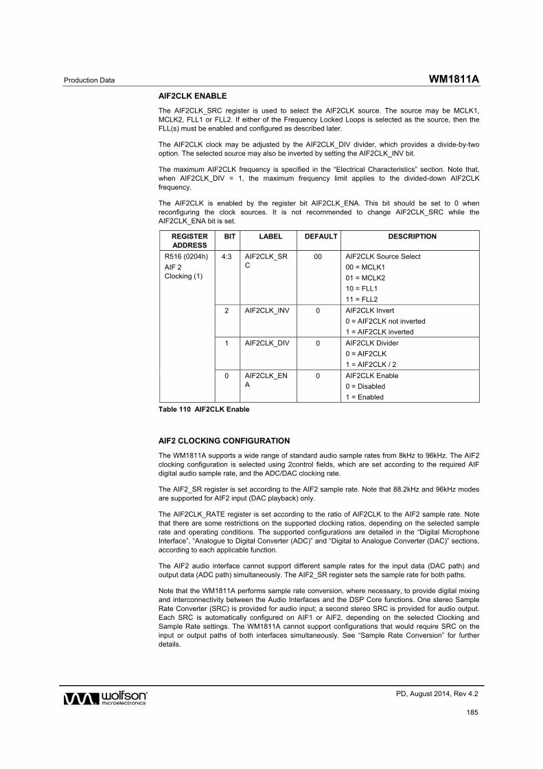
Production Data WM1811A
w PD, August 2014, Rev 4.2
185
AIF2CLK ENABLE
The AIF2CLK_SRC register is used to select the AIF2CLK source. The source may be MCLK1, MCLK2, FLL1 or FLL2. If either of the Frequency Locked Loops is selected as the source, then the FLL(s) must be enabled and configured as described later.
The AIF2CLK clock may be adjusted by the AIF2CLK_DIV divider, which provides a divide-by-two option. The selected source may also be inverted by setting the AIF2CLK_INV bit.
The maximum AIF2CLK frequency is specified in the “Electrical Characteristics” section. Note that, when AIF2CLK_DIV = 1, the maximum frequency limit applies to the divided-down AIF2CLK frequency.
The AIF2CLK is enabled by the register bit AIF2CLK_ENA. This bit should be set to 0 when reconfiguring the clock sources. It is not recommended to change AIF2CLK_SRC while the AIF2CLK_ENA bit is set.
REGISTER ADDRESS
BIT LABEL DEFAULT DESCRIPTION
R516 (0204h)
AIF 2 Clocking (1)
4:3 AIF2CLK_SRC
00 AIF2CLK Source Select
00 = MCLK1
01 = MCLK2
10 = FLL1
11 = FLL2
2 AIF2CLK_INV 0 AIF2CLK Invert
0 = AIF2CLK not inverted
1 = AIF2CLK inverted
1 AIF2CLK_DIV 0 AIF2CLK Divider
0 = AIF2CLK
1 = AIF2CLK / 2
0 AIF2CLK_ENA
0 AIF2CLK Enable
0 = Disabled
1 = Enabled
Table 110 AIF2CLK Enable
AIF2 CLOCKING CONFIGURATION
The WM1811A supports a wide range of standard audio sample rates from 8kHz to 96kHz. The AIF2 clocking configuration is selected using 2control fields, which are set according to the required AIF digital audio sample rate, and the ADC/DAC clocking rate.
The AIF2_SR register is set according to the AIF2 sample rate. Note that 88.2kHz and 96kHz modes are supported for AIF2 input (DAC playback) only.
The AIF2CLK_RATE register is set according to the ratio of AIF2CLK to the AIF2 sample rate. Note that there are some restrictions on the supported clocking ratios, depending on the selected sample rate and operating conditions. The supported configurations are detailed in the “Digital Microphone Interface”, “Analogue to Digital Converter (ADC)” and “Digital to Analogue Converter (DAC)” sections, according to each applicable function.
The AIF2 audio interface cannot support different sample rates for the input data (DAC path) and output data (ADC path) simultaneously. The AIF2_SR register sets the sample rate for both paths.
Note that the WM1811A performs sample rate conversion, where necessary, to provide digital mixing and interconnectivity between the Audio Interfaces and the DSP Core functions. One stereo Sample Rate Converter (SRC) is provided for audio input; a second stereo SRC is provided for audio output. Each SRC is automatically configured on AIF1 or AIF2, depending on the selected Clocking and Sample Rate settings. The WM1811A cannot support configurations that would require SRC on the input or output paths of both interfaces simultaneously. See “Sample Rate Conversion” for further details.

WM1811A Production Data
w PD, August 2014, Rev 4.2
186
REGISTER ADDRESS
BIT LABEL DEFAULT DESCRIPTION
R529 (0211h)
AIF2 Rate
7:4 AIF2_SR 1000 Selects the AIF2 Sample Rate (fs)
0000 = 8kHz
0001 = 11.025kHz
0010 = 12kHz
0011 = 16kHz
0100 = 22.05kHz
0101 = 24kHz
0110 = 32kHz
0111 = 44.1kHz
1000 = 48kHz
1001 = 88.2kHz
1010 = 96kHz
All other codes = Reserved
Note that 88.2kHz and 96kHz modes are supported for AIF2 input (DAC playback) only.
3:0 AIF2CLK_RATE
0011 Selects the AIF2CLK / fs ratio
0000 = Reserved
0001 = 128
0010 = 192
0011 = 256
0100 = 384
0101 = 512
0110 = 768
0111 = 1024
1000 = 1408
1001 = 1536
All other codes = Reserved
Table 111 AIF2 Clocking Configuration
MISCELLANEOUS CLOCK CONTROLS
SYSCLK provides clocking for many of the WM1811A functions. SYSCLK clock is required to support DSP Core functions and also the Charge Pump, Class D switching amplifier, DC servo control and other internal functions.
The SYSCLK_SRC register is used to select the SYSCLK source. The source may be AIF1CLK or AIF2CLK, as illustrated in Figure 68. Note that the bandwidth of the digital audio mixing paths will be determined by the sample rate of whichever AIF is selected as the SYSCLK source. When using only one audio interface, the active interface should be selected as the SYSCLK source. For best audio performance when using AIF1 and AIF2 simultaneously, the SYSCLK source must select the AIF with the highest sample rate (AIFn_SR).
The AIF1 DSP processing clock is derived from SYSCLK, and enabled by AIF1DSPCLK_ENA.
The AIF2 DSP processing clock is derived from SYSCLK, and enabled by AIF2DSPCLK_ENA.
The clocking of the WM1811A ADC, DAC, digital mixer and digital microphone functions is enabled by setting SYSDSPCLK_ENA. See “Digital Microphone Interface” for details of the DMICCLK frequency.
Two modes of ADC / Digital Microphone operation can be selected using the ADC_OSR128 bit. This bit is enabled by default, giving best audio performance. De-selecting this bit provides a low power alternative setting.
A high performance mode of DAC operation can be selected by setting the DAC_OSR128 bit. When the DAC_OSR128 bit is set, the audio performance is improved, but power consumption is also increased.

Production Data WM1811A
w PD, August 2014, Rev 4.2
187
A clock is required for the Charge Pump circuit when the ground-referenced headphone outputs (HPOUT1L and HPOUT1R) are enabled. The Charge Pump clock is derived from SYSCLK whenever the Charge Pump is enabled. The Charge Pump clock division is configured automatically.
A clock is required for the Class D speaker driver circuit when the speaker outputs (SPKOUTL and SPKOUTR) are enabled. The Class D clock is derived from SYSCLK whenever these outputs are enabled in Class D mode. The Class D clock division is configured automatically. See “Analogue Outputs” for details of the Class D switching frequency.
A clock output (OPCLK) derived from SYSCLK may be output on a GPIO pin. This clock is enabled by register big OPCLK_ENA, and its frequency of this clock is controlled by OPCLK_DIV. See General Purpose Input/Output” to configure a GPIO pin for this function.
A slow clock (TOCLK) is derived internally in order to control volume update timeouts when the zero-cross option is selected. This clock is enabled by register bit TOCLK_ENA, and its frequency is controlled by TOCLK_DIV.
A de-bounce control is provided for GPIO inputs and for other functions that may be selected as GPIO outputs. The de-bounced clock frequency is controlled by DBCLK_DIV.
The WM1811A generates a 256kHz clock for internal functions; TOCLK and DBCLK are derived from this 256kHz clock. In order to generate this clock correctly when SYSCLK_SRC = 0, valid settings are required for AIF1_SR and AIF1CLK_RATE. To generate this clock correctly when SYSCLK_SRC = 1, valid settings are required for AIF2_SR and AIF2CLK_RATE.
The WM1811A Clocking is illustrated in Figure 68.
Figure 68 System Clocking
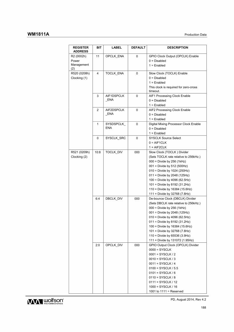
WM1811A Production Data
w PD, August 2014, Rev 4.2
188
REGISTER ADDRESS
BIT LABEL DEFAULT DESCRIPTION
R2 (0002h)
Power Management (2)
11 OPCLK_ENA 0 GPIO Clock Output (OPCLK) Enable
0 = Disabled
1 = Enabled
R520 (0208h)
Clocking (1)
4 TOCLK_ENA 0 Slow Clock (TOCLK) Enable
0 = Disabled
1 = Enabled
This clock is required for zero-cross timeout.
3 AIF1DSPCLK_ENA
0 AIF1 Processing Clock Enable
0 = Disabled
1 = Enabled
2 AIF2DSPCLK_ENA
0 AIF2 Processing Clock Enable
0 = Disabled
1 = Enabled
1 SYSDSPCLK_ENA
0 Digital Mixing Processor Clock Enable
0 = Disabled
1 = Enabled
0 SYSCLK_SRC 0 SYSCLK Source Select
0 = AIF1CLK
1 = AIF2CLK
R521 (0209h)
Clocking (2)
10:8 TOCLK_DIV 000 Slow Clock (TOCLK ) Divider
(Sets TOCLK rate relative to 256kHz.)
000 = Divide by 256 (1kHz)
001 = Divide by 512 (500Hz)
010 = Divide by 1024 (250Hz)
011 = Divide by 2048 (125Hz)
100 = Divide by 4096 (62.5Hz)
101 = Divide by 8192 (31.2Hz)
110 = Divide by 16384 (15.6Hz)
111 = Divide by 32768 (7.8Hz)
6:4 DBCLK_DIV 000 De-bounce Clock (DBCLK) Divider
(Sets DBCLK rate relative to 256kHz.)
000 = Divide by 256 (1kHz)
001 = Divide by 2048 (125Hz)
010 = Divide by 4096 (62.5Hz)
011 = Divide by 8192 (31.2Hz)
100 = Divide by 16384 (15.6Hz)
101 = Divide by 32768 (7.8Hz)
110 = Divide by 65536 (3.9Hz)
111 = Divide by 131072 (1.95Hz)
2:0 OPCLK_DIV 000 GPIO Output Clock (OPCLK) Divider
0000 = SYSCLK
0001 = SYSCLK / 2
0010 = SYSCLK / 3
0011 = SYSCLK / 4
0100 = SYSCLK / 5.5
0101 = SYSCLK / 6
0110 = SYSCLK / 8
0111 = SYSCLK / 12
1000 = SYSCLK / 16
1001 to 1111 = Reserved

Production Data WM1811A
w PD, August 2014, Rev 4.2
189
REGISTER ADDRESS
BIT LABEL DEFAULT DESCRIPTION
R1568 (0620h)
Oversampling
1 ADC_OSR128 1 ADC / Digital Microphone Oversample Rate Select
0 = Low Power
1 = High Performance
0 DAC_OSR128 0 DAC Oversample Rate Select
0 = Low Power
1 = High Performance
R1793 (0701h)
Pull Control (MCLK2)
14 MCLK2_PU 0 MCLK2Pull-up enable
0 = Disabled
1 = Enabled
13 MCLK2_PD 1 MCLK2Pull-down enable
0 = Disabled
1 = Enabled
R1824 (0720h)
Pull Control (1)
7 MCLK1_PU 0 MCLK1 Pull-up enable
0 = Disabled
1 = Enabled
6 MCLK1_PD 0 MCLK1 Pull-down enable
0 = Disabled
1 = Enabled
Table 112 System Clocking
BCLK AND LRCLK CONTROL
The digital audio interfaces (AIF1 and AIF2) use BCLK and LRCLK signals for synchronisation. In master mode, these are output signals, generated by the WM1811A. In slave mode, these are input signals to the WM1811A. It is also possible to support mixed master/slave operation.
The BCLK and LRCLK signals are controlled as illustrated in Figure 69. See the “Digital Audio Interface Control” section for further details of the relevant control registers.
Figure 69 BCLK and LRCLK Control
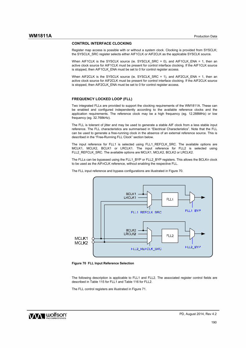
WM1811A Production Data
w PD, August 2014, Rev 4.2
190
CONTROL INTERFACE CLOCKING
Register map access is possible with or without a system clock. Clocking is provided from SYSCLK; the SYSCLK_SRC register selects either AIF1CLK or AIF2CLK as the applicable SYSCLK source.
When AIF1CLK is the SYSCLK source (ie. SYSCLK_SRC = 0), and AIF1CLK_ENA = 1, then an active clock source for AIF1CLK must be present for control interface clocking. If the AIF1CLK source is stopped, then AIF1CLK_ENA must be set to 0 for control register access.
When AIF2CLK is the SYSCLK source (ie. SYSCLK_SRC = 1), and AIF2CLK_ENA = 1, then an active clock source for AIF2CLK must be present for control interface clocking. If the AIF2CLK source is stopped, then AIF2CLK_ENA must be set to 0 for control register access.
FREQUENCY LOCKED LOOP (FLL)
Two integrated FLLs are provided to support the clocking requirements of the WM1811A. These can be enabled and configured independently according to the available reference clocks and the application requirements. The reference clock may be a high frequency (eg. 12.288MHz) or low frequency (eg. 32.768kHz).
The FLL is tolerant of jitter and may be used to generate a stable AIF clock from a less stable input reference. The FLL characteristics are summarised in “Electrical Characteristics”. Note that the FLL can be used to generate a free-running clock in the absence of an external reference source. This is described in the “Free-Running FLL Clock” section below.
The input reference for FLL1 is selected using FLL1_REFCLK_SRC. The available options are MCLK1, MCLK2, BCLK1 or LRCLK1. The input reference for FLL2 is selected using FLL2_REFCLK_SRC. The available options are MCLK1, MCLK2, BCLK2 or LRCLK2.
The FLLs can be bypassed using the FLL1_BYP or FLL2_BYP registers. This allows the BCLKn clock to be used as the AIFnCLK reference, without enabling the respective FLL.
The FLL input reference and bypass configurations are illustrated in Figure 70.
Figure 70 FLL Input Reference Selection
The following description is applicable to FLL1 and FLL2. The associated register control fields are described in Table 115 for FLL1 and Table 116 for FLL2.
The FLL control registers are illustrated in Figure 71.

Production Data WM1811A
w PD, August 2014, Rev 4.2
191
Figure 71 FLL Configuration
The FLL is enabled using the FLLn_ENA register bit (where n = 1 for FLL1 and n = 2 for FLL2). Note that the other FLL registers should be configured before enabling the FLL; the FLLn_ENA register bit should be set as the final step of the FLLn enable sequence.
When changing FLL settings, it is recommended that the digital circuit be disabled via FLLn_ENA and then re-enabled after the other register settings have been updated. When changing the input reference frequency FREF, it is recommended that the FLL be reset by setting FLLn_ENA to 0.
The field FLLn_REFCLK_DIV provides the option to divide the input reference (MCLK, BCLK or LRCLK) by 1, 2, 4 or 8. This field should be set to bring the reference down to 13.5MHz or below. For best performance, it is recommended that the highest possible frequency - within the 13.5MHz limit - should be selected.
The FLL output frequency is directly determined from FLLn_FRATIO, FLLn_OUTDIV and the real number represented by N.K.
The integer value, N, is held in the FLLn_N register field. The fractional portion, K, is determined by the ratio FLLn_THETA / FLLn_LAMBDA.
Note that the FLLn_EFS_ENA register bit must be enabled in fractional mode (ie. whenever FLLn_THETA > 0).
The FLL output frequency is generated according to the following equation:
FOUT = (FVCO / FLLn_OUTDIV)
The FLLoperating frequency, FVCO is set according to the following equation:
FVCO = (FREF x N.K x FLLn_FRATIO)
FREF is the input frequency, as determined by FLLn_REFCLK_DIV.
FVCO must be in the range 90-100 MHz. Frequencies outside this range cannot be supported.
Note that the output frequencies that do not lie within the ranges quoted above cannot be guaranteed across the full range of device operating conditions.

WM1811A Production Data
w PD, August 2014, Rev 4.2
192
In order to follow the above requirements for FVCO, the value of FLLn_OUTDIV should be selected according to the desired output FOUT. The divider, FLLn_OUTDIV, must be set so that FVCO is in the range 90-100MHz. The available divisions are integers from 4 to 64. Some typical settings of FLLn_OUTDIV are noted in Table 113.
OUTPUT FREQUENCY FOUT FLLn_OUTDIV
1.875 MHz - 2.0833 MHz 101111 (divide by 48)
2.8125 MHz - 3.125 MHz 011111 (divide by 32)
3.75 MHz - 4.1667 MHz 010111 (divide by 24)
5.625 MHz - 6.25 MHz 001111 (divide by 16)
11.25 MHz - 12.5 MHz 000111 (divide by 8)
18 MHz - 20 MHz 000100 (divide by 5)
22.5 MHz - 25 MHz 000011 (divide by 4)
Table 113 Selection of FLLn_OUTDIV
The value of FLLn_FRATIO should be selected as described in Table 114.
REFERENCE FREQUENCY FREF FLLn_FRATIO
1MHz - 13.5MHz 0h (divide by 1)
256kHz - 1MHz 1h (divide by 2)
128kHz - 256kHz 2h (divide by 4)
64kHz - 128kHz 3h (divide by 8)
Less than 64kHz 4h (divide by 16)
Table 114 Selection of FLLn_FRATIO
In order to determine the remaining FLL parameters, the FLL operating frequency, FVCO, must be calculated, as given by the following equation:
FVCO = (FOUT x FLLn_OUTDIV)
The value of N.K can then be determined as follows:
N.K = FVCO / (FLLn_FRATIO x FREF)
Note that, in the above equations:
FLLn_OUTDIV is the FOUT clock ratio.
FREF is the input frequency, after division by FLL_REFCLK_DIV, where applicable.
FLLn_FRATIO is the FVCO clock ratio (1, 2, 4, 8 or 16).
The value of N is held in the FLLn_N register field.
The value of K is determined by the ratio FLLn_THETA / FLLn_LAMBDA.
The FLLn_N, FLLn_THETA and FLLn_LAMBDA fields are all coded as integers (LSB = 1).

Production Data WM1811A
w PD, August 2014, Rev 4.2
193
In Fractional Mode (FLLn_THETA > 0 and FLLn_EFS_ENA = 1), the register fields FLLn_THETA and FLLn_LAMBDA can be calculated as follows:
Calculate GCD(FLL) using the ‘Greatest Common Denominator’ function:
GCD(FLL) = GCD(FLLn_FRATIO x FREF, FVCO)
where GCD(x, y) is the greatest common denominator of x and y
Next, calculate FLLn_THETA and FLLn_LAMBDA using the following equations:
FLLn_THETA = (FVCO - (FLLn_N x FLLn_FRATIO x FREF)) / GCD(FLL)
FLLn_LAMBDA = (FLLn_FRATIO x FREF) / GCD(FLL)
Note that, in Fractional Mode, the values of FLLn_THETA and FLLn_LAMBDA must be co-prime (ie. not divisible by any common integer). The calculation above ensures that the values will be co-prime.
The value of K must be a fraction less than 1 (ie. FLLn_THETA must be less than FLLn_LAMBDA).
The FLL1 control registers are described in Table 115. The FLL2 control registers are described in Table 116. Example settings for a variety of reference frequencies and output frequencies are shown in Table 118.
REGISTER ADDRESS
BIT LABEL DEFAULT DESCRIPTION
R544 (0220h)
FLL1 Control (1)
0 FLL1_ENA 0 FLL1 Enable
0 = Disabled
1 = Enabled
This should be set as the final step of the FLL1 enable sequence, ie. after the other FLL registers have been configured.
R545 (0221h)
FLL1 Control (2)
13:8 FLL1_OUTDIV [5:0]
000000 FLL1 FOUT clock divider 000000 = Reserved 000001 = Reserved 000010 = Reserved 000011 = 4 000100 = 5 000101 = 6 … 111110 = 63 111111 = 64 (FOUT = FVCO / FLL1_OUTDIV)
2:0 FLL1_FRATIO [2:0]
000 FLL1 FVCO clock divider
000 = 1
001 = 2
010 = 4
011 = 8
1XX = 16
R546 (0222h)
FLL1 Control (3)
15:0 FLL1_THETA[15:0]
0000h FLL Fractional multiply for FREF
This field sets the numerator (multiply) part of the FLL1_THETA / FLL1_LAMBDA ratio.
Coded as LSB = 1.
R547 (0223h)
FLL1 Control (4)
14:5 FLL1_N[9:0] 000h FLL Integer multiply for FREF
(LSB = 1)

WM1811A Production Data
w PD, August 2014, Rev 4.2
194
REGISTER ADDRESS
BIT LABEL DEFAULT DESCRIPTION
R548 (0224h)
FLL1 Control (5)
15 FLL1_BYP 0 FLL1 Bypass Select
0 = Disabled
1 = Enabled
When FLL1_BYP is set, the FLL1 output is derived directly from BCLK1. In this case, FLL1 can be disabled.
4:3 FLL1_REFCLK_DIV [1:0]
00 FLL1 Clock Reference Divider
00 = MCLK / 1
01 = MCLK / 2
10 = MCLK / 4
11 = MCLK / 8
MCLK (or other input reference) must be divided down to <=13.5MHz.
For lower power operation, the reference clock can be divided down further if desired.
1:0 FLL1_REFCLK_SRC [1:0]
00 FLL1 Clock source
00 = MCLK1
01 = MCLK2
10 = LRCLK1
11 = BCLK1
R550 (0226h)
FLL1 EFS1
15:0 FLL1_LAMBDA [15:0]
0000h FLL Fractional multiply for FREF
This field sets the denominator (dividing) part of the FLL1_THETA / FLL1_LAMBDA ratio.
Coded as LSB = 1.
R551 (0227h)
FLL1 EFS2
2:1 11 Reserved - Do not change
0 FLL1_EFS_ENA 0 FLL Fractional Mode EFS enable
0 = Integer Mode
1 = Fractional Mode
This bit should be set to 1 when FLL1_THETA > 0.
Table 115 FLL1 Register Map

Production Data WM1811A
w PD, August 2014, Rev 4.2
195
REGISTER ADDRESS
BIT LABEL DEFAULT DESCRIPTION
R576 (0240h)
FLL2 Control (1)
0 FLL2_ENA 0 FLL2 Enable
0 = Disabled
1 = Enabled
This should be set as the final step of the FLL2 enable sequence, ie. after the other FLL registers have been configured.
R577 (0241h)
FLL2 Control (2)
13:8 FLL2_OUTDIV [5:0]
000000 FLL2 FOUT clock divider
000000 = Reserved
000001 = Reserved
000010 = Reserved
000011 = 4
000100 = 5
000101 = 6
…
111110 = 63
111111 = 64
(FOUT = FVCO / FLL2_OUTDIV)
2:0 FLL2_FRATIO [2:0]
000 FLL2 FVCO clock divider
000 = 1
001 = 2
010 = 4
011 = 8
1XX = 16
R578 (0242h)
FLL2 Control (3)
15:0 FLL2_THETA[15:0]
0000h FLL Fractional multiply for FREF
This field sets the numerator (multiply) part of the FLL2_THETA / FLL2_LAMBDA ratio.
Coded as LSB = 1.
R579 (0243h)
FLL2 Control (4)
14:5 FLL2_N[9:0] 000h FLL Integer multiply for FREF
(LSB = 1)
R580 (0244h)
FLL2 Control (5)
15 FLL2_BYP 0 FLL2 Bypass Select
0 = Disabled
1 = Enabled
When FLL2_BYP is set, the FLL2 output is derived directly from BCLK2. In this case, FLL2 can be disabled.
4:3 FLL2_REFCLK_DIV [1:0]
00 FLL2 Clock Reference Divider
00 = MCLK / 1
01 = MCLK / 2
10 = MCLK / 4
11 = MCLK / 8
MCLK (or other input reference) must be divided down to <=13.5MHz.
For lower power operation, the reference clock can be divided down further if desired.
1:0 FLL2_REFCLK_SRC [1:0]
00 FLL2 Clock source
00 = MCLK1
01 = MCLK2
10 = LRCLK2
11 = BCLK2
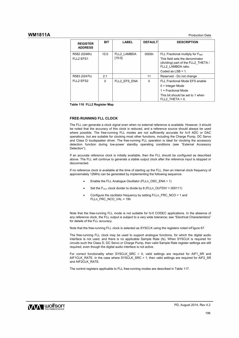
WM1811A Production Data
w PD, August 2014, Rev 4.2
196
REGISTER ADDRESS
BIT LABEL DEFAULT DESCRIPTION
R582 (0246h)
FLL2 EFS1
15:0 FLL2_LAMBDA [15:0]
0000h FLL Fractional multiply for FREF
This field sets the denominator (dividing) part of the FLL2_THETA / FLL2_LAMBDA ratio.
Coded as LSB = 1.
R583 (0247h)
FLL2 EFS2
2:1 11 Reserved - Do not change
0 FLL2_EFS_ENA 0 FLL Fractional Mode EFS enable
0 = Integer Mode
1 = Fractional Mode
This bit should be set to 1 when FLL2_THETA > 0.
Table 116 FLL2 Register Map
FREE-RUNNING FLL CLOCK
The FLL can generate a clock signal even when no external reference is available. However, it should be noted that the accuracy of this clock is reduced, and a reference source should always be used where possible. The free-running FLL modes are not sufficiently accurate for hi-fi ADC or DAC operations, but are suitable for clocking most other functions, including the Charge Pump, DC Servo and Class D loudspeaker driver. The free-running FLL operation is ideal for clocking the accessory detection function during low-power standby operating conditions (see “External Accessory Detection”).
If an accurate reference clock is initially available, then the FLL should be configured as described above. The FLL will continue to generate a stable output clock after the reference input is stopped or disconnected.
If no reference clock is available at the time of starting up the FLL, then an internal clock frequency of approximately 12MHz can be generated by implementing the following sequence:
Enable the FLL Analogue Oscillator (FLLn_OSC_ENA = 1)
Set the FOUT clock divider to divide by 8 (FLLn_OUTDIV = 000111)
Configure the oscillator frequency by setting FLLn_FRC_NCO = 1 and FLLn_FRC_NCO_VAL = 19h
Note that the free-running FLL mode is not suitable for hi-fi CODEC applications. In the absence of any reference clock, the FLL output is subject to a very wide tolerance; see “Electrical Characteristics” for details of the FLL accuracy.
Note that the free-running FLL clock is selected as SYSCLK using the registers noted inFigure 67.
The free-running FLL clock may be used to support analogue functions, for which the digital audio interface is not used, and there is no applicable Sample Rate (fs). When SYSCLK is required for circuits such the Class D, DC Servo or Charge Pump, then valid Sample Rate register settings are still required, even though the digital audio interface is not active.
For correct functionality when SYSCLK_SRC = 0, valid settings are required for AIF1_SR and AIF1CLK_RATE. In the case where SYSCLK_SRC = 1, then valid settings are required for AIF2_SR and AIF2CLK_RATE.
The control registers applicable to FLL free-running modes are described in Table 117.

Production Data WM1811A
w PD, August 2014, Rev 4.2
197
REGISTER ADDRESS
BIT LABEL DEFAULT DESCRIPTION
R544 (0220h)
FLL1 Control (1)
1 FLL1_OSC_ENA 0 FLL1Oscillator enable
0 = Disabled
1 = Enabled
(Note that this field is required for free-running FLL1 modes only)
R548 (0224h)
FLL1 Control (5)
12:7 FLL1_FRC_NCO_VAL [5:0]
19h FLL1 Forced oscillator value
Valid range is 000000 to 111111
0x19h (011001) = 12MHz approx
(Note that this field is required for free-running FLL modes only)
6 FLL1_FRC_NCO 0 FLL1Forced control select
0 = Normal
1 = FLL1 oscillator controlled by FLL1_FRC_NCO_VAL
(Note that this field is required for free-running FLL modes only)
R576 (0240h)
FLL2 Control (1)
1 FLL2_OSC_ENA 0 FLL2 Oscillator enable
0 = Disabled
1 = Enabled
(Note that this field is required for free-running FLL2 modes only)
R580 (0244h)
FLL2 Control (5)
12:7 FLL2_FRC_NCO_VAL [5:0]
19h FLL2 Forced oscillator value
Valid range is 000000 to 111111
0x19h (011001) = 12MHz approx
(Note that this field is required for free-running FLL modes only)
6 FLL2_FRC_NCO 0 FLL2 Forced control select
0 = Normal
1 = FLL2 oscillator controlled by FLL2_FRC_NCO_VAL
(Note that this field is required for free-running FLL modes only)
Table 117 FLL Free-Running Mode
GPIO OUTPUTS FROM FLL
For each FLL, the WM1811A has an internal signal which indicates whether the FLL Lock has been achieved. The FLL Lock status is an input to the Interrupt control circuit and can be used to trigger an Interrupt event - see “Interrupts”.
The FLL Lock signal can be output directly on a GPIO pin as an external indication of FLL Lock. See “General Purpose Input/Output” for details of how to configure a GPIO pin to output the FLL Lock signal.
The FLL Clock can be output directly on a GPIO pin as a clock signal for other circuits. Note that the FLL Clock may be output even if the FLL is not selected as the WM1811A SYSCLK source. The FLL clocking configuration is illustrated in Figure 70. See “General Purpose Input/Output” for details of how to configure a GPIO pin to output the FLL Clock.

WM1811A Production Data
w PD, August 2014, Rev 4.2
198
EXAMPLE FLL CALCULATION
The following example illustrates how to derive the FLL1 registers to generate 12.288 MHz output (FOUT) from a 12.000 MHz reference clock (FREF):
Set FLL1_REFCLK_DIV in order to generate FREF<=13.5MHz: FLL1_REFCLK_DIV = 00 (divide by 1)
Set FLL1_OUTDIV for the required output frequency as shown in Table 113:- FOUT = 12.288 MHz, therefore FLL1_OUTDIV = 7h (divide by 8)
Set FLL1_FRATIO for the given reference frequency as shown in Table 114: FREF = 12MHz, therefore FLL1_FRATIO = 0h (divide by 1)
Calculate FVCO as given by FVCO = FOUT x FLL1_OUTDIV:- FVCO = 12.288 x 8 = 98.304MHz
Calculate N.K as given by N.K = FVCO / (FLL1_FRATIO x FREF): N.K = 98.304 / (1 x 12) = 8.192
Set FLL1_EFS_ENA according to whether N.K is an integer. N.K has a fractional part, therefore FLL1_EFS_ENA = 1
Determine FLL1_N from the integer portion of N.K:- FLL_N =8.
Determine GCD(FLL), as given by GCD(FLL) = GCD(FLL1_FRATIO x FREF, FVCO): GCD(FLL)= GCD(1 x 12000000, 98304000) = 96000
Determine FLL1_THETA, as given by FLL1_THETA = (FVCO - (FLL1_N x FLL1_FRATIO x FREF)) / GCD(FLL): FLL1_THETA = (98304000 - (8 x 1 x 12000000)) / 96000 FLL1_THETA = 24 (0018h)
Determine FLL_LAMBDA, as given by FLL1_LAMBDA = (FLL1_FRATIO x FREF) / GCD(FLL): FLL1_LAMBDA = (1 x 12000000) / 96000 FLL1_LAMBDA = 125 (007Dh)
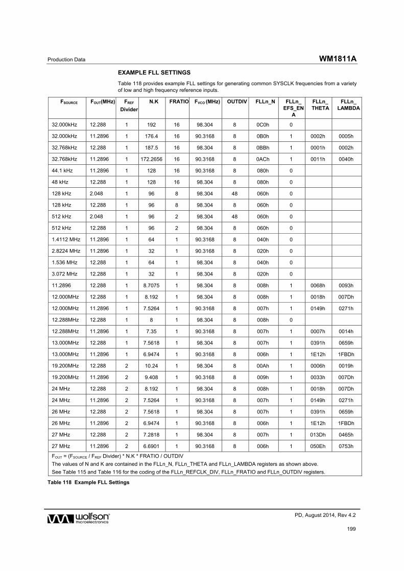
Production Data WM1811A
w PD, August 2014, Rev 4.2
199
EXAMPLE FLL SETTINGS
Table 118 provides example FLL settings for generating common SYSCLK frequencies from a variety of low and high frequency reference inputs.
FSOURCE FOUT(MHz) FREF
Divider
N.K FRATIO FVCO (MHz) OUTDIV FLLn_N FLLn_ EFS_EN
A
FLLn_ THETA
FLLn_LAMBDA
32.000kHz 12.288 1 192 16 98.304 8 0C0h 0
32.000kHz 11.2896 1 176.4 16 90.3168 8 0B0h 1 0002h 0005h
32.768kHz 12.288 1 187.5 16 98.304 8 0BBh 1 0001h 0002h
32.768kHz 11.2896 1 172.2656 16 90.3168 8 0ACh 1 0011h 0040h
44.1 kHz 11.2896 1 128 16 90.3168 8 080h 0
48 kHz 12.288 1 128 16 98.304 8 080h 0
128 kHz 2.048 1 96 8 98.304 48 060h 0
128 kHz 12.288 1 96 8 98.304 8 060h 0
512 kHz 2.048 1 96 2 98.304 48 060h 0
512 kHz 12.288 1 96 2 98.304 8 060h 0
1.4112 MHz 11.2896 1 64 1 90.3168 8 040h 0
2.8224 MHz 11.2896 1 32 1 90.3168 8 020h 0
1.536 MHz 12.288 1 64 1 98.304 8 040h 0
3.072 MHz 12.288 1 32 1 98.304 8 020h 0
11.2896 12.288 1 8.7075 1 98.304 8 008h 1 0068h 0093h
12.000MHz 12.288 1 8.192 1 98.304 8 008h 1 0018h 007Dh
12.000MHz 11.2896 1 7.5264 1 90.3168 8 007h 1 0149h 0271h
12.288MHz 12.288 1 8 1 98.304 8 008h 0
12.288MHz 11.2896 1 7.35 1 90.3168 8 007h 1 0007h 0014h
13.000MHz 12.288 1 7.5618 1 98.304 8 007h 1 0391h 0659h
13.000MHz 11.2896 1 6.9474 1 90.3168 8 006h 1 1E12h 1FBDh
19.200MHz 12.288 2 10.24 1 98.304 8 00Ah 1 0006h 0019h
19.200MHz 11.2896 2 9.408 1 90.3168 8 009h 1 0033h 007Dh
24 MHz 12.288 2 8.192 1 98.304 8 008h 1 0018h 007Dh
24 MHz 11.2896 2 7.5264 1 90.3168 8 007h 1 0149h 0271h
26 MHz 12.288 2 7.5618 1 98.304 8 007h 1 0391h 0659h
26 MHz 11.2896 2 6.9474 1 90.3168 8 006h 1 1E12h 1FBDh
27 MHz 12.288 2 7.2818 1 98.304 8 007h 1 013Dh 0465h
27 MHz 11.2896 2 6.6901 1 90.3168 8 006h 1 050Eh 0753h
FOUT = (FSOURCE / FREF Divider) * N.K * FRATIO / OUTDIV
The values of N and K are contained in the FLLn_N, FLLn_THETA and FLLn_LAMBDA registers as shown above.
See Table 115 and Table 116 for the coding of the FLLn_REFCLK_DIV, FLLn_FRATIO and FLLn_OUTDIV registers.
Table 118 Example FLL Settings
WM1811A Production Data
w PD, August 2014, Rev 4.2
200
SAMPLE RATE CONVERSION
The WM1811A supports two main digital audio interfaces, AIF1 and AIF2. These interfaces are configured independently and may operate entirely asynchronously to each other. The WM1811A performs stereo full-duplex sample rate conversion between the audio interfaces, allowing digital audio to be routed between the interfaces, and allowing asynchronous audio data to be mixed together.
The Sample Rate Converters (SRCs) are configured automatically within the WM1811A, and no user settings are required. The SRCs are enabled automatically when required and are disabled at other times. Synchronisation between the audio interfaces is not instantaneous when the clocking or sample rate configurations are updated; the lock status of the SRCs is signalled via the GPIO or Interrupt circuits, as described in “General Purpose Input/Output” and “Interrupts”.
Separate clocks can be used for AIF1 and AIF2, allowing asynchronous operation on these interfaces. The digital mixing core is clocked by SYSCLK, which is linked to either AIF1CLK or AIF2CLK, as described in “Clocking and Sample Rates”. The digital mixing core is, therefore, always synchronised to AIF1, or to AIF2, or to both interfaces at once.
SAMPLE RATE CONVERTER 1 (SRC1)
SRC1 performs sample rate conversion of digital audio data input to the WM1811A. Sample Rate Conversion is required when digital audio data is received on an audio interface that is not synchronised to the digital mixing core.
SRC1 is automatically configured on AIF1 or AIF2, depending on the selected Clocking and Sample Rate configuration. Note that SRC1 cannot convert input data on AIF1 and AIF2 simultaneously.
The SRC1 Lock status indicates when audio data can be received on the interface channel that is not synchronised to the digital mixing core. No audio will be present on this signal path until SRC1 Lock is achieved.
SAMPLE RATE CONVERTER 2 (SRC2)
SRC2 performs sample rate conversion of digital audio data output from the WM1811A. Sample Rate Conversion is required when digital audio data is transmitted on an audio interface that is not synchronised to the digital mixing core.
SRC2 is automatically configured on AIF1 or AIF2, depending on the selected Clocking and Sample Rate configuration. Note that SRC2 cannot convert output data on AIF1 and AIF2 simultaneously.
The SRC2 Lock status indicates when audio data can be transmitted on the interface channel that is not synchronised to the digital mixing core. No audio will be present on this signal path until SRC2 Lock is achieved.

Production Data WM1811A
w PD, August 2014, Rev 4.2
201
SAMPLE RATE CONVERTER RESTRICTIONS
The following restrictions apply to the configuration of the WM1811A Sample Rate Converters.
No SRC capability when using 88.2kHz or 96kHz AIF input (DAC playback). If either interface is configured for 88.2kHz or 96kHz sample rate, then the digital mixing core must also be configured for this sample rate. Sample Rate Conversion cannot be supported in this mode, therefore AIF output is not supported at any sample rate under these conditions.
Restricted Sample Rate options when AIF1 and AIF2 are not synchronised. When a different clock source is used for AIF1CLK and AIF2CLK, then the AIF to which the SYSCLK is synchronised cannot be mixed sample rates.
If AIF1CLK_SRC ≠ AIF2CLK_SRC
And SYSCLK_SRC =0
Then AIF1DAC_DIV and AIF1ADC_DIV must be set to 000
SAMPLE RATE CONVERTER CONFIGURATION ERROR INDICATION
The WM1811A verifies the register settings relating to Clocking, Sample Rates and Sample Rate Conversion. If an invalid configuration is attempted, then the SR_ERROR register will indicate the error by showing a non-zero value. This read-only field may be checked to confirm that the WM1811A can support the selected Clocking and Sample Rate settings.
REGISTER ADDRESS
BIT LABEL DEFAULT DESCRIPTION
R530 (0212h)
Rate Status
3:0 SR_ERROR [3:0]
0000 Sample Rate Configuration status
Indicates an error with the register settings related to sample rate configuration
0000 = No errors
0001 = Invalid sample rate
0010 = Invalid AIF divide
0011 = ADC and DAC divides both set in an interface
0100 = Invalid combination of AIF divides and sample-rate
0101 = Invalid set of enables for 96kHz mode
0110 = Invalid SYSCLK rate (derived from AIF1CLK_RATE or AIF2CLK_RATE)
0111 = Mixed ADC and DAC rates in SYSCLK AIF when AIFs are asynchronous
1000 = Invalid combination of sample rates when both AIFs are from the same clock source
1001 = Invalid combination of mixed ADC/DAC AIFs when both from the same clock source
Table 119 Sample Rate Converter Configuration Status
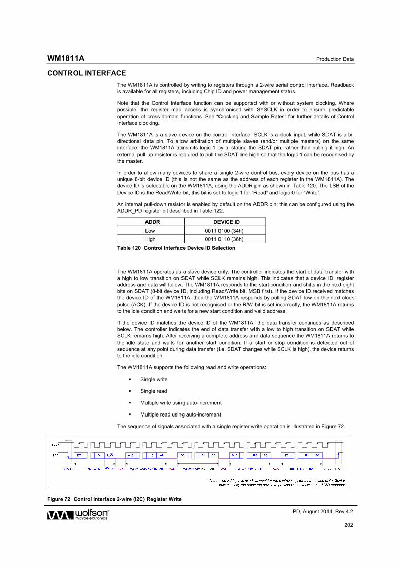
WM1811A Production Data
w PD, August 2014, Rev 4.2
202
CONTROL INTERFACE
The WM1811A is controlled by writing to registers through a 2-wire serial control interface. Readback is available for all registers, including Chip ID and power management status.
Note that the Control Interface function can be supported with or without system clocking. Where possible, the register map access is synchronised with SYSCLK in order to ensure predictable operation of cross-domain functions. See “Clocking and Sample Rates” for further details of Control Interface clocking.
The WM1811A is a slave device on the control interface; SCLK is a clock input, while SDAT is a bi-directional data pin. To allow arbitration of multiple slaves (and/or multiple masters) on the same interface, the WM1811A transmits logic 1 by tri-stating the SDAT pin, rather than pulling it high. An external pull-up resistor is required to pull the SDAT line high so that the logic 1 can be recognised by the master.
In order to allow many devices to share a single 2-wire control bus, every device on the bus has a unique 8-bit device ID (this is not the same as the address of each register in the WM1811A). The device ID is selectable on the WM1811A, using the ADDR pin as shown in Table 120. The LSB of the Device ID is the Read/Write bit; this bit is set to logic 1 for “Read” and logic 0 for “Write”.
An internal pull-down resistor is enabled by default on the ADDR pin; this can be configured using the ADDR_PD register bit described in Table 122.
ADDR DEVICE ID
Low 0011 0100 (34h)
High 0011 0110 (36h)
Table 120 Control Interface Device ID Selection
The WM1811A operates as a slave device only. The controller indicates the start of data transfer with a high to low transition on SDAT while SCLK remains high. This indicates that a device ID, register address and data will follow. The WM1811A responds to the start condition and shifts in the next eight bits on SDAT (8-bit device ID, including Read/Write bit, MSB first). If the device ID received matches the device ID of the WM1811A, then the WM1811A responds by pulling SDAT low on the next clock pulse (ACK). If the device ID is not recognised or the R/W bit is set incorrectly, the WM1811A returns to the idle condition and waits for a new start condition and valid address.
If the device ID matches the device ID of the WM1811A, the data transfer continues as described below. The controller indicates the end of data transfer with a low to high transition on SDAT while SCLK remains high. After receiving a complete address and data sequence the WM1811A returns to the idle state and waits for another start condition. If a start or stop condition is detected out of sequence at any point during data transfer (i.e. SDAT changes while SCLK is high), the device returns to the idle condition.
The WM1811A supports the following read and write operations:
Single write
Single read
Multiple write using auto-increment
Multiple read using auto-increment
The sequence of signals associated with a single register write operation is illustrated in Figure 72.
Figure 72 Control Interface 2-wire (I2C) Register Write

Production Data WM1811A
w PD, August 2014, Rev 4.2
203
The sequence of signals associated with a single register read operation is illustrated in Figure 73.
Figure 73 Control Interface 2-wire (I2C) Register Read
The Control Interface also supports other register operations, as listed above. The interface protocol for these operations is summarised below. The terminology used in the following figures is detailed in Table 121.
Note that, for multiple write and multiple read operations, the auto-increment option must be enabled. This feature is enabled by default, as noted inTable 122.
TERMINOLOGY DESCRIPTION
S Start Condition
Sr Repeated start
A Acknowledge (SDA Low)
A Not Acknowledge (SDA High)
P Stop Condition
R/W ReadNotWrite
0 = Write
1 = Read
[White field] Data flow from bus master to WM1811A
[Grey field] Data flow from WM1811A to bus master
Table 121 Control Interface Terminology
Figure 74 Single Register Write to Specified Address
Figure 75 Single Register Read from Specified Address

WM1811A Production Data
w PD, August 2014, Rev 4.2
204
Figure 76 Multiple Register Write to Specified Address using Auto-increment
Figure 77 Multiple Register Read from Specified Address using Auto-increment
Figure 78 Multiple Register Read from Last Address using Auto-increment
Multiple Write and Multiple Read operations enable the host processor to access sequential blocks of the data in the WM1811A register map faster than is possible with single register operations. The auto-increment option is enabled when the AUTO_INC register bit is set. This bit is defined in Table 122. Auto-increment is enabled by default.
REGISTER ADDRESS
BIT LABEL DEFAULT DESCRIPTION
R257 (0101h)
Control Interface
2 AUTO_INC 1 Enables address auto-increment
0 = Disabled
1 = Enabled
R1825 (0721h)
Pull Control (2)
8 ADDR_PD 1 ADDR Pull-down enable
0 = Disabled
1 = Enabled
Table 122 Control Interface Configuration

Production Data WM1811A
w PD, August 2014, Rev 4.2
205
POP SUPPRESSION CONTROL
The WM1811A incorporates a number of features, including Wolfson’s SilentSwitch™ technology, designed to suppress pops normally associated with Start-Up, Shut-Down or signal path control. Note that, to achieve maximum benefit from these features, careful attention is required to the sequence and timing of these controls.
The Pop Suppression controls relating to the Headphone / Line Output drivers are described in the “Analogue Output Signal Path” section.
Additional bias controls are described in the “Reference Voltages and Master Bias” section.
DISABLED LINE OUTPUT CONTROL
The line outputs are biased to VMID in normal operation. To avoid audible pops caused by a disabled signal path dropping to AGND, the WM1811A can maintain these connections at VMID when the relevant output stage is disabled. This is achieved by connecting a buffered VMID reference to the output.
The buffered VMID reference is enabled by setting VMID_BUF_ENA. The output resistance is selectable, using the VROI register bit.
Note that, if LINEOUTn_DISCH=1 (see Table 124), then the respective output will be discharged to AGND, and will not be connected to VMID.
REGISTER ADDRESS
BIT LABEL DEFAULT DESCRIPTION
R55 (0037h)
Additional Control
0 VROI 0 Buffered VMID to Analogue Line Output Resistance (Disabled Outputs)
0 = 20k from buffered VMID to output
1 = 500 from buffered VMID to output
R57 (0039h)
AntiPOP (2)
3 VMID_BUF_ENA
0 VMID Buffer Enable
0 = Disabled
1 = Enabled (provided VMID_SEL > 00)
Table 123 Disabled Line Output Control

WM1811A Production Data
w PD, August 2014, Rev 4.2
206
LINE OUTPUT DISCHARGE CONTROL
The line output paths can be actively discharged to AGND through internal resistors if desired. This is desirable at start-up in order to achieve a known output stage condition prior to enabling the soft-start VMID reference voltage. This is also desirable in shut-down to prevent the external connections from being affected by the internal circuits.
The line outputs LINEOUT1P and LINEOUT1N are discharged to AGND by setting LINEOUT1_DISCH. The line outputs LINEOUT2P and LINEOUT2N are discharged to AGND by setting LINEOUT2_DISCH.
The discharge resistance is dependent upon the respective LINEOUTn_ENA bit, and also according to the VROI bit (see Table 123). The discharge resistance is noted in the “Electrical Characteristics” section.
REGISTER ADDRESS
BIT LABEL DEFAULT DESCRIPTION
R56 (0038h)
AntiPOP (1)
5 LINEOUT1_DISCH
0 Discharges LINEOUT1P and LINEOUT1N outputs
0 = Not active
1 = Actively discharging LINEOUT1P and LINEOUT1N
4 LINEOUT2_DISCH
0 Discharges LINEOUT2P and LINEOUT2N outputs
0 = Not active
1 = Actively discharging LINEOUT2P and LINEOUT2N
Table 124 Line Output Discharge Control
VMID REFERENCE DISCHARGE CONTROL
The VMID reference can be actively discharged to AGND through internal resistors. This is desirable at start-up in order to achieve a known initial condition prior to enabling the soft-start VMID reference; this ensures maximum suppression of audible pops associated with start-up. VMID is discharged by setting VMID_DISCH.
REGISTER ADDRESS
BIT LABEL DEFAULT DESCRIPTION
R57 (0039h)
AntiPOP (2)
0 VMID_DISCH 0 Connects VMID to ground
0 = Disabled
1 = Enabled
Table 125 VMID Reference Discharge Control
INPUT VMID CLAMPS
The analogue inputs can be clamped to Vmid using the INPUTS_CLAMP bit described below. This allows pre-charging of the input AC coupling capacitors during power-up. Note that all eight inputs are clamped using the same control bit.
Note that INPUTS_CLAMP must be set to 0 when the analogue input signal paths are in use.
REGISTER
ADDRESS
BIT LABEL DEFAULT DESCRIPTION
R21 (15h)
Input Mixer (1)
6 INPUTS_CLAMP 0 Input pad VMID clamp
0 = Clamp de-activated
1 = Clamp activated
Table 126 Input VMID Clamps

Production Data WM1811A
w PD, August 2014, Rev 4.2
207
LDO REGULATORS
The WM1811A provides two integrated Low Drop-Out Regulators (LDOs). These are provided to generate the appropriate power supplies for internal circuits, simplifying and reducing the requirements for external supplies and associated components. A reference circuit powered by AVDD2 ensures the accuracy of the LDO regulator voltage settings.
Note that the integrated LDOs are only intended for generating the AVDD1 and DCVDD supply rails for the WM1811A; they are not suitable for powering any additional or external loads.
LDO1 is intended for generating AVDD1 - the primary analogue power domain of the WM1811A. LDO1 is powered by LDO1VDD and is enabled when a logic ‘1’ is applied to the LDO1ENA pin. The logic level is determined with respect to the DBVDD1 voltage domain. The LDO1 start-up time is dependent on the external AVDD1 and VREFC capacitors; the start-up time is noted in the “Electrical Characteristics” section for the recommended external component conditions.
When LDO1 is enabled, the output voltage is controlled by the LDO1_VSEL register field. Note that the LDO1 voltage difference LDO1VDD - AVDD1 must be higher than the LDO1 Drop-Out voltage (see “Electrical Characteristics”).
When LDO1 is disabled(by applying a logic ‘0’ to the LDO1ENA pin), the output can be left floating or can be actively discharged, depending on the LDO1_DISCH control bit.
It is possible to supply AVDD1 from an external supply. If AVDD1 is supplied externally, then LDO1 should be disabled, and the LDO1 output left floating (LDO1DISCH = 0). Note that the LDO1VDD voltage must be greater than or equal to AVDD1; this ensures that there is no leakage path through the LDO for the external supply.
Note that the WM1811A can operate with AVDD1 tied to 0V; power consumption may be reduced, but the analogue audio functions will not be supported.
LDO2 is intended for generating the DCVDD power domain which supplies the digital core functions on the WM1811A. LDO2 is powered by DBVDD1 and is enabled when a logic ‘1’ is applied to the LDO2ENA pin. The logic level is determined with respect to the DBVDD1 voltage domain.The LDO2 start-up time is dependent on the external DCVDD and VREFC capacitors; the start-up time is noted in the “Electrical Characteristics” section for the recommended external component conditions.
When LDO2 is enabled, the output voltage is controlled by the LDO2_VSEL register field.
When LDO2 is disabled (by applying a logic ‘0’ to the LDO2ENA pin), the output can be left floating or can be actively discharged, depending on the LDO2_DISCH control bit.
It is possible to supply DCVDD from an external supply. If DCVDD is supplied externally, the LDO2ENA and LDO2DISCH bits should be set to 0. Note that the DBVDD1 voltage must be greater than or equal to DCVDD; this ensures that there is no leakage path through the LDO for the external supply.
An internal pull-down resistor is enabled by default on the LDO1ENA and LDO2ENA pins. These pull-down resistors can be configured using the register bits described in Table 127.
Decoupling capacitors should be connected to the voltage reference pin, VREFC, and also to the LDO outputs, AVDD1 and DCVDD. See “Applications Information” for further details.
The LDO Regulator connections and controls are illustrated in Figure 79. The register controls are defined in Table 127.

WM1811A Production Data
w PD, August 2014, Rev 4.2
208
AVDD2
VREFCVoltage
Reference
LDO1VDD
LDO1
AVDD1 DBVDD1
LDO2
DCVDD
Digital Core SupplyAnalogue Supply
LDO1ENA LDO2ENA
LDO1_VSEL[2:0]LDO1_DISCH
LDO2_VSEL[1:0]LDO2_DISCH
Figure 79 LDO Regulators
REGISTER ADDRESS
BIT LABEL DEFAULT DESCRIPTION
R59 (003Bh)
LDO 1
3:1 LDO1_VSEL [2:0] 110 LDO1 Output Voltage Select
2.4V to 3.1V in 100mV steps
000 = 2.4V
001 = 2.5V
010 = 2.6V
011 = 2.7V
100 = 2.8V
101 = 2.9V
110 = 3.0V
111 = 3.1V
0 LDO1_DISCH 1 LDO1 Discharge Select
0 = LDO1 floating when disabled
1 = LDO1 discharged when disabled
R60 (003Ch)
LDO 2
2:1 LDO2_VSEL [1:0] 01 LDO2 Output Voltage Select
1.05V to 1.25V in 100mV steps
00 = Reserved
01 = 1.05V
10 = 1.15V
11 = 1.25V
0 LDO2_DISCH 1 LDO2 Discharge Select
0 = LDO2 floating when disabled
1 = LDO2 discharged when disabled
R1825 (0721h)
Pull Control (2)
6 LDO2ENA_PD 1 LDO2ENA Pull-down enable
0 = Disabled
1 = Enabled
4 LDO1ENA_PD 1 LDO1ENA Pull-down enable
0 = Disabled
1 = Enabled
Table 127 LDO Regulator Control

Production Data WM1811A
w PD, August 2014, Rev 4.2
209
REFERENCE VOLTAGES AND MASTER BIAS
This section describes the analogue reference voltage and bias current controls. It also describes the VMID soft-start circuit for pop suppressed start-up and shut-down.
The analogue circuits in the WM1811A require a mid-rail analogue reference voltage, VMID. This reference is generated from AVDD1 via a programmable resistor chain. Together with the external VMID decoupling capacitor, the programmable resistor chain determines the charging characteristic on VMID. This is controlled by VMID_SEL[1:0], and can be used to optimise the reference for normal operation or low power standby as described in Table 128.
A buffered mid-rail reference voltage is provided. This is required for the single-ended configuration of the Input PGAs, and also for direct signal paths from the input pins to the Input Mixers, Output Mixers or Speaker Mixers. These requirements are noted in the relevant “Analogue Input Signal Path” and “Analogue Output Signal Path” sections. The buffered mid-rail reference is enabled by setting the VMID_BUF_ENA register bit.
The analogue circuits in the WM1811A require a bias current. The normal bias current is enabled by setting BIAS_ENA. Note that the normal bias current source requires VMID to be enabled also.
REGISTER ADDRESS
BIT LABEL DEFAULT
DESCRIPTION
R1 (0001h)
Power Management (1)
2:1 VMID_SEL [1:0]
00 VMID Divider Enable and Select
00 = VMID disabled (for OFF mode)
01 = 2 x 40k divider (for normal operation)
10 = 2 x 240k divider (for low power standby)
11 = Reserved
0 BIAS_ENA 0 Enables the Normal bias current generator (for all analogue functions)
0 = Disabled
1 = Enabled
R57 (0039h)
AntiPOP (2)
3 VMID_BUF_ENA
0 VMID Buffer Enable
0 = Disabled
1 = Enabled (provided VMID_SEL > 00)
Table 128 Reference Voltages and Master Bias Enable
A pop-suppressed start-up requires VMID to be enabled smoothly, without the step change normally associated with the initial stage of the VMID capacitor charging. A pop-suppressed start-up also requires the analogue bias current to be enabled throughout the signal path prior to the VMID reference voltage being applied. The WM1811A incorporates pop-suppression circuits which address these requirements.
An alternate bias current source (Start-Up Bias) is provided for pop-free start-up; this is enabled by the STARTUP_BIAS_ENA register bit. The start-up bias is selected (in place of the normal bias) using the BIAS_SRC bit. It is recommended that the start-up bias is used during start-up, before switching back to the higher quality, normal bias.
A soft-start circuit is provided in order to control the switch-on of the VMID reference. The soft-start control circuit offers two slew rates for enabling the VMID reference; these are selected and enabled by VMID_RAMP. When the soft-start circuit is enabled prior to enabling VMID_SEL, the reference voltage rises smoothly, without the step change that would otherwise occur. It is recommended that the soft-start circuit and the output signal path be enabled before VMID is enabled by VMID_SEL.
A soft shut-down is provided, using the soft-start control circuit and the start-up bias current generator. The soft shut-down of VMID is achieved by setting VMID_RAMP, STARTUP_BIAS_ENA and BIAS_SRC to select the start-up bias current and soft-start circuit prior to setting VMID_SEL=00.
Note that, if the VMID_RAMP function is enabled for soft start-up or soft shut-down then, after setting VMID_SEL = 00 to disable VMID, the soft-start circuit must be reset before re-enabling VMID. The soft-start circuit is reset by setting VMID_RAMP = 00. After resetting the soft-start circuit, the VMID_RAMP register may be updated to the required setting for the next VMID transition.
The VMID soft-start register controls are defined in Table 129.
WM1811A Production Data
w PD, August 2014, Rev 4.2
210
REGISTER ADDRESS
BIT LABEL DEFAULT DESCRIPTION
R57 (0039h)
AntiPOP (2)
6:5 VMID_RAMP [1:0] 10 VMID soft start enable / slew rate control
00 = Normal slow start
01 = Normal fast start
10 = Soft slow start
11 = Soft fast start
If VMID_RAMP = 1X is selected for VMID start-up or shut-down, then the soft-start circuit must be reset by setting VMID_RAMP=00 after VMID is disabled, before VMID is re-enabled. VMID is disabled / enabled using the VMID_SEL register.
2 STARTUP_BIAS_ENA
0 Enables the Start-Up bias current generator
0 = Disabled
1 = Enabled
1 BIAS_SRC 1 Selects the bias current source
0 = Normal bias
1 = Start-Up bias
Table 129 Soft Start Control
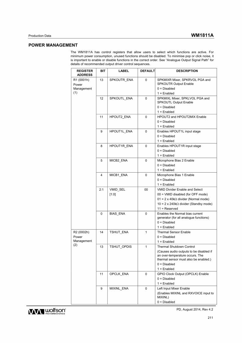
Production Data WM1811A
w PD, August 2014, Rev 4.2
211
POWER MANAGEMENT
The WM1811A has control registers that allow users to select which functions are active. For minimum power consumption, unused functions should be disabled. To minimise pop or click noise, it is important to enable or disable functions in the correct order. See “Analogue Output Signal Path” for details of recommended output driver control sequences.
REGISTER ADDRESS
BIT LABEL DEFAULT DESCRIPTION
R1 (0001h)
Power Management (1)
13 SPKOUTR_ENA 0 SPKMIXR Mixer, SPKRVOL PGA and SPKOUTR Output Enable
0 = Disabled
1 = Enabled
12 SPKOUTL_ENA 0 SPKMIXL Mixer, SPKLVOL PGA and SPKOUTL Output Enable
0 = Disabled
1 = Enabled
11 HPOUT2_ENA 0 HPOUT2 and HPOUT2MIX Enable
0 = Disabled
1 = Enabled
9 HPOUT1L_ENA 0 Enables HPOUT1L input stage
0 = Disabled
1 = Enabled
8 HPOUT1R_ENA 0 Enables HPOUT1R input stage
0 = Disabled
1 = Enabled
5 MICB2_ENA 0 Microphone Bias 2 Enable
0 = Disabled
1 = Enabled
4 MICB1_ENA 0 Microphone Bias 1 Enable
0 = Disabled
1 = Enabled
2:1 VMID_SEL
[1:0]
00 VMID Divider Enable and Select
00 = VMID disabled (for OFF mode)
01 = 2 x 40k divider (Normal mode)
10 = 2 x 240k divider (Standby mode)
11 = Reserved
0 BIAS_ENA 0 Enables the Normal bias current generator (for all analogue functions)
0 = Disabled
1 = Enabled
R2 (0002h)
Power Management (2)
14 TSHUT_ENA 1 Thermal Sensor Enable
0 = Disabled
1 = Enabled
13 TSHUT_OPDIS 1 Thermal Shutdown Control
(Causes audio outputs to be disabled if an over-temperature occurs. The thermal sensor must also be enabled.)
0 = Disabled
1 = Enabled
11 OPCLK_ENA 0 GPIO Clock Output (OPCLK) Enable
0 = Disabled
1 = Enabled
9 MIXINL_ENA 0 Left Input Mixer Enable
(Enables MIXINL and RXVOICE input to MIXINL)
0 = Disabled
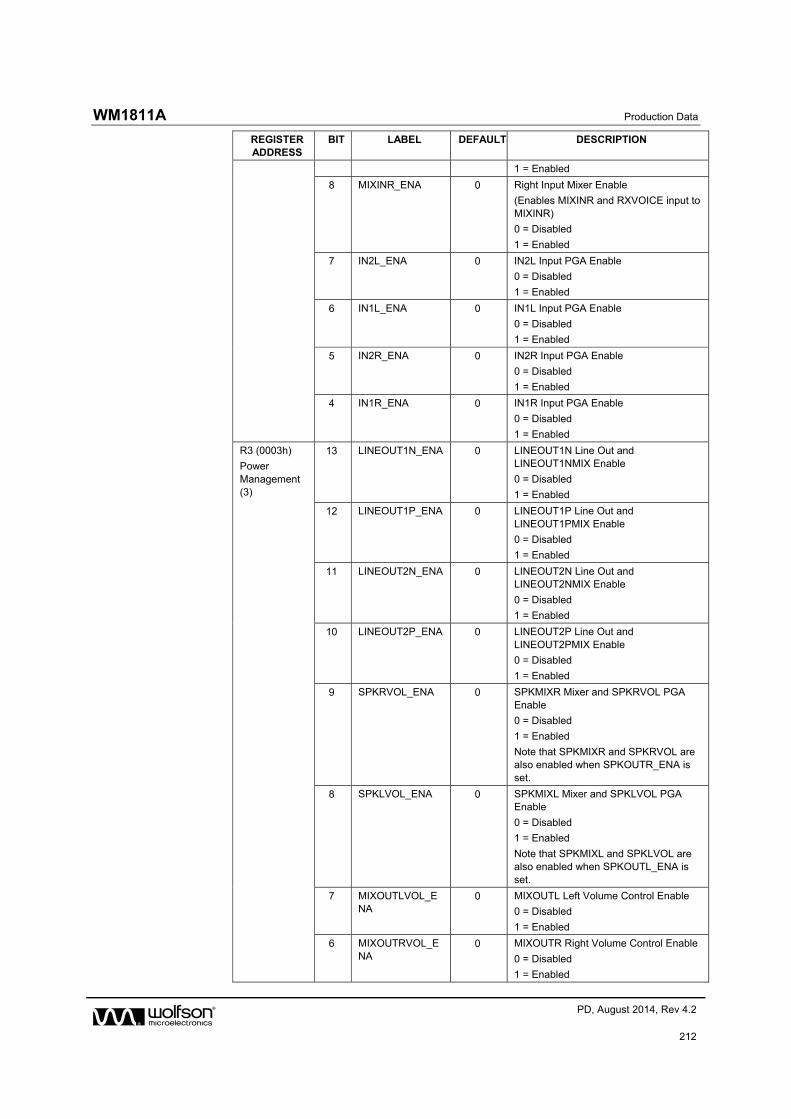
WM1811A Production Data
w PD, August 2014, Rev 4.2
212
REGISTER ADDRESS
BIT LABEL DEFAULT DESCRIPTION
1 = Enabled
8 MIXINR_ENA 0 Right Input Mixer Enable
(Enables MIXINR and RXVOICE input to MIXINR)
0 = Disabled
1 = Enabled
7 IN2L_ENA 0 IN2L Input PGA Enable
0 = Disabled
1 = Enabled
6 IN1L_ENA 0 IN1L Input PGA Enable
0 = Disabled
1 = Enabled
5 IN2R_ENA 0 IN2R Input PGA Enable
0 = Disabled
1 = Enabled
4 IN1R_ENA 0 IN1R Input PGA Enable
0 = Disabled
1 = Enabled
R3 (0003h)
Power Management (3)
13 LINEOUT1N_ENA 0 LINEOUT1N Line Out and LINEOUT1NMIX Enable
0 = Disabled
1 = Enabled
12 LINEOUT1P_ENA 0 LINEOUT1P Line Out and LINEOUT1PMIX Enable
0 = Disabled
1 = Enabled
11 LINEOUT2N_ENA 0 LINEOUT2N Line Out and LINEOUT2NMIX Enable
0 = Disabled
1 = Enabled
10 LINEOUT2P_ENA 0 LINEOUT2P Line Out and LINEOUT2PMIX Enable
0 = Disabled
1 = Enabled
9 SPKRVOL_ENA 0 SPKMIXR Mixer and SPKRVOL PGA Enable
0 = Disabled
1 = Enabled
Note that SPKMIXR and SPKRVOL are also enabled when SPKOUTR_ENA is set.
8 SPKLVOL_ENA 0 SPKMIXL Mixer and SPKLVOL PGA Enable
0 = Disabled
1 = Enabled
Note that SPKMIXL and SPKLVOL are also enabled when SPKOUTL_ENA is set.
7 MIXOUTLVOL_ENA
0 MIXOUTL Left Volume Control Enable
0 = Disabled
1 = Enabled
6 MIXOUTRVOL_ENA
0 MIXOUTR Right Volume Control Enable
0 = Disabled
1 = Enabled

Production Data WM1811A
w PD, August 2014, Rev 4.2
213
REGISTER ADDRESS
BIT LABEL DEFAULT DESCRIPTION
5 MIXOUTL_ENA 0 MIXOUTL Left Output Mixer Enable
0 = Disabled
1 = Enabled
4 MIXOUTR_ENA 0 MIXOUTR Right Output Mixer Enable
0 = Disabled
1 = Enabled
R4 (0004h)
Power Management (4)
13 AIF2ADCL_ENA 0 Enable AIF2ADC (Left) output path
0 = Disabled
1 = Enabled
This bit must be set for AIF2 or AIF3 output of the AIF2ADC (Left) signal.
12 AIF2ADCR_ENA 0 Enable AIF2ADC (Right) output path
0 = Disabled
1 = Enabled
This bit must be set for AIF2 or AIF3 output of the AIF2ADC (Left) signal.
9 AIF1ADC1L_ENA 0 Enable AIF1ADC (Left) output path
0 = Disabled
1 = Enabled
8 AIF1ADC1L_ENA 0 Enable AIF1ADC (Right) output path
0 = Disabled
1 = Enabled
3 DMIC1L_ENA 0 Digital microphone (DMICDAT) Left channel enable
0 = Disabled
1 = Enabled
2 DMIC1R_ENA 0 Digital microphone (DMICDAT) Right channel enable
0 = Disabled
1 = Enabled
1 ADCL_ENA 0 Left ADC Enable
0 = Disabled
1 = Enabled
0 ADCR_ENA 0 Right ADC Enable
0 = Disabled
1 = Enabled
R5 (0005h)
Power Management (5)
13 AIF2DACL_ENA 0 Enable AIF2DAC (Left) input path
0 = Disabled
1 = Enabled
12 AIF2DACR_ENA 0 Enable AIF2DAC (Right) input path
0 = Disabled
1 = Enabled
9 AIF1DAC1L_ENA 0 Enable AIF1DAC (Left) input path
0 = Disabled
1 = Enabled
8 AIF1DAC1R_ENA 0 Enable AIF1DAC (Right) input path
0 = Disabled
1 = Enabled
1 DAC1L_ENA 0 Left DAC Enable
0 = Disabled
1 = Enabled
0 DAC1R_ENA 0 Right DAC Enable
0 = Disabled

WM1811A Production Data
w PD, August 2014, Rev 4.2
214
REGISTER ADDRESS
BIT LABEL DEFAULT DESCRIPTION
1 = Enabled
R76 (004Ch)
Charge Pump (1)
15 CP_ENA 0 Enable charge-pump digits
0 = Disable
1 = Enable
R84 (0054h)
DC Servo (1)
1 DCS_ENA_CHAN_1
0 DC Servo enable for HPOUT1R
0 = Disabled
1 = Enabled
0 DCS_ENA_CHAN_0
0 DC Servo enable for HPOUT1L
0 = Disabled
1 = Enabled
R512 (0200h)
AIF 1 Clocking (1)
0 AIF1CLK_ENA 0 AIF1CLK Enable
0 = Disabled
1 = Enabled
R516 (0204h)
AIF 2 Clocking (1)
0 AIF2CLK_ENA 0 AIF2CLK Enable
0 = Disabled
1 = Enabled
R520 (0208h)
Clocking (1)
4 TOCLK_ENA 0 Slow Clock (TOCLK) Enable
0 = Disabled
1 = Enabled
This clock is required for zero-cross timeout.
3 AIF1DSPCLK_ENA
0 AIF1 Processing Clock Enable
0 = Disabled
1 = Enabled
2 AIF2DSPCLK_ENA
0 AIF2 Processing Clock Enable
0 = Disabled
1 = Enabled
1 SYSDSPCLK_ENA
0 Digital Mixing Processor Clock Enable
0 = Disabled
1 = Enabled
R544 (0220h)
FLL1 Control (1)
0 FLL1_ENA 0 FLL1 Enable
0 = Disabled
1 = Enabled
This should be set as the final step of the FLL1 enable sequence, ie. after the other FLL registers have been configured.
R576 (0240h)
FLL2 Control (1)
0 FLL2_ENA 0 FLL2 Enable
0 = Disabled
1 = Enabled
This should be set as the final step of the FLL2 enable sequence, ie. after the other FLL registers have been configured.
Table 130 Power Management

Production Data WM1811A
w PD, August 2014, Rev 4.2
215
THERMAL SHUTDOWN
The WM1811A incorporates a temperature sensor which detects when the device temperature is within normal limits or if the device is approaching a hazardous temperature condition. The temperature sensor can be configured to automatically disable the audio outputs of the WM1811A in response to an overtemperature condition (approximately 150ºC).
The temperature status can be output directly on a GPIO pin, as described in the “General Purpose Input/Output” section. The temperature sensor can also be used to generate Interrupt events, as described in the “Interrupts” section. The GPIO and Interrupt functions can be used to indicate either a Warning Temperature event or the Shutdown Temperature event.
The temperature sensor is enabled by setting the TSHUT_ENA register bit. When the TSHUT_OPDIS is also set, then a device over-temperature condition will cause the speaker outputs (SPKOUTL and SPKOUTR) of the WM1811A to be disabled; this response is likely to prevent any damage to the device attributable to the large currents of the output drivers.
Note that, to prevent pops and clicks, TSHUT_ENA and TSHUT_OPDIS should only be updated whilst the speaker and headphone outputs are disabled.
REGISTER ADDRESS
BIT LABEL DEFAULT DESCRIPTION
R2 (0002h)
Power Management (2)
14 TSHUT_ENA 1 Thermal sensor enable
0 = Disabled
1 = Enabled
13 TSHUT_OPDIS 1 Thermal shutdown control
(Causes audio outputs to be disabled if an overtemperature occurs. The thermal sensor must also be enabled.)
0 = Disabled
1 = Enabled
Table 131 Thermal Shutdown

WM1811A Production Data
w PD, August 2014, Rev 4.2
216
POWER ON RESET
The WM1811A includes a Power-On Reset (POR) circuit, which isused to reset the digital logic into a default state after power up. The POR circuit derives its output from AVDD2 and DCVDD. The internal POR¯¯¯ signal is asserted low when AVDD2 and DCVDD are below minimum thresholds.
The specific behaviour of the circuit will vary, depending on relative timing of the supply voltages. Typical scenarios are illustrated in Figure 80 and Figure 81.
Figure 80 Power On Reset Timing – AVDD2 enabled/disabled first
DCVDD
0V
AVDD2
0V
Vpora
Vpord_off
LO
HI
Internal POR
Device ready
Vpora_on
POR active POR active
POR undefined
Figure 81 Power On Reset Timing - DCVDD enabled/disabled first
The POR¯¯¯ signal is undefined until AVDD2 has exceeded the minimum threshold, Vpora. Once this threshold has been exceeded, POR¯¯¯ is asserted low and the chip is held in reset. In this condition, all writes to the control interface are ignored. Once AVDD2 and DCVDD have reached their respective power on thresholds, POR¯¯¯ is released high, all registers are in their default state, and writes to the control interface may take place.
Note that a power-on reset period, TPOR, applies afterAVDD2 and DCVDD have reached their respective power on thresholds. This specification is guaranteed by design rather than test.
On power down, POR¯¯¯ is asserted low when either AVDD2 or DCVDD falls below their respective power-down thresholds.

Production Data WM1811A
w PD, August 2014, Rev 4.2
217
Typical Power-On Reset parameters for the WM1811A are defined in Table 132.
SYMBOL DESCRIPTION TYP UNIT
Vpora_on Power-On threshold (AVDD2) 1.15 V
Vpora_off Power-Off threshold (AVDD2) 1.14 V
Vpord_on Power-On threshold (DCVDD) 0.56 V
Vpord_off Power-Off threshold (DCVDD) 0.55 V
TPOR Minimum Power-On Reset period 100 ns
Table 132 Typical Power-On Reset Parameters
Table 133 describes the status of the WM1811A digital I/O pins when the Power On Reset has completed, prior to any register writes. The same conditions apply on completion of a Software Reset (described in the “Software Reset and Device ID” section).
PIN NO NAME TYPE RESET STATUS
DBVDD1 power domain
D5 SPKMODE Digital Input Pull-up to DBVDD1
A4 LDO1ENA Digital Input Pull-down to DGND
F3 ADDR Digital Input Pull-down to DGND
D6 LDO2ENA Digital Input Pull-down to DGND
H2 SCLK Digital Input Digital input
H3 SDA Digital Input/Output Digital input
F1 MCLK1 Digital Input Digital input
F2 MCLK2 Digital Input Pull-down to DGND
G3 BCLK1 Digital Input/Output Digital input
G1 LRCLK1 Digital Input/Output Digital input
J1 ADCLRCLK1/GPIO1 Digital Input/Output Digital input
H1 DACDAT1 Digital Input Digital input
F4 ADCDAT1 Digital Output Digital output
DBVDD2 power domain
K1 BCLK2 Digital Input/Output Digital input, Pull-down to DGND
J3 LRCLK2 Digital Input/Output Digital input, Pull-down to DGND
G4 DACDAT2 Digital Input Pull-down to DGND
H4 ADCDAT2 Digital Output Digital output
DBVDD3 power domain
K4 GPIO11/BCLK3 Digital Input/Output Digital input, Pull-down to DGND
G5 GPIO10/LRCLK3 Digital Input/Output Digital input, Pull-down to DGND
K3 GPIO8/DACDAT3 Digital Input/Output Digital input, Pull-down to DGND
J4 GPIO9/ADCDAT3 Digital Input/Output Digital input, Pull-down to DGND
MICBIAS1 power domain
A8 DMICCLK Digital Output Digital output
C8 IN2LN/DMICDAT Analogue Input/Digital Input Analogue input
Table 133 WM1811A Digital I/O Status in Reset
Note that the dual function IN2LN/DMICDAT pin defaults to IN2LN (analogue input) after Power On Reset is completed. The IN2LN function is referenced to the AVDD1 power domain.

WM1811A Production Data
w PD, August 2014, Rev 4.2
218
SOFTWARE RESET AND DEVICE ID
The device ID can be read back from register R0. Writing to this register will reset the device.
The software reset causes all control registers to be reset to their default state.
The status of the WM1811A digital I/O pins following a software reset is described in Table 133.
The Customer ID and Device Revision can be read back from register R256.
REGISTER ADDRESS
BIT LABEL DEFAULT DESCRIPTION
R0 (0000h)
Software Reset
15:0 SW_RESET [15:0]
1811h Writing to this register resets all registers to their default state.
Reading from this register will indicate device ID 1811h.
R256 (0100h)
Chip Revision
15:8 CUST_ID [7:0] Customer ID
3:0 CHIP_REV [3:0] Chip revision
Table 134 Chip Reset and ID

Production Data WM1811A
w PD, August 2014, Rev 4.2
219
REGISTER MAP
The WM1811A control registers are listed below. Note that only the register addresses described here should be accessed; writing to
other addresses may result in undefined behaviour. Register bits that are not documented should not be changed from the default
values.
REG NAME 15 14 13 12 11 10 9 8 7 6 5 4 3 2 1 0 DEFAULT
R0 (0h) Software Reset SW_RESET [15:0] 0000h
R1 (1h) Power Management (1)
0 0 SPKOUTR_ENA
SPKOUTL_E
NA
HPOUT2_EN
A
0 HPOUT1L_E
NA
HPOUT1R_E
NA
0 0 MICB2_ENA
MICB1_ENA
0 VMID_SEL [1:0]
BIAS_ENA
0000h
R2 (2h) Power Management (2)
0 TSHU
T_ENA TSHU
T_OPDIS
0 OPCL
K_ENA
0 MIXIN
L_ENA MIXIN
R_ENA
IN2L_
ENA
IN1L_
ENA
IN2R_
ENA
IN1R_
ENA
0 0 0 0 6000h
R3 (3h) Power
Management (3) 0 0 LINEO
UT1N_ENA
LINEO
UT1P_ENA
LINEO
UT2N_ENA
LINEO
UT2P_ENA
SPKR
VOL_ENA
SPKLV
OL_ENA
MIXO
UTLVOL_E
NA
MIXO
UTRVOL_E
NA
MIXO
UTL_ENA
MIXO
UTR_ENA
0 0 0 0 0000h
R4 (4h) Power Management (4)
0 0 AIF2A
DCL_ENA
AIF2A
DCR_ENA
0 0 AIF1A
DC1L_ENA
AIF1A
DC1R_ENA
0 0 0 0 DMIC1
L_ENA
DMIC1
R_ENA
ADCL_
ENA
ADCR
_ENA
0000h
R5 (5h) Power
Management (5) 0 0 AIF2D
ACL_ENA
AIF2D
ACR_ENA
0 0 AIF1D
AC1L_ENA
AIF1D
AC1R_ENA
0 0 0 0 0 0 DAC1L
_ENA
DAC1
R_ENA
0000h
R6 (6h) Power
Management (6) 0 0 0 0 0 AIF3ADC_SRC
[1:0] AIF2DAC_SRC
[1:0] 0 AIF3_
TRI AIF3_ADCDAT
_SRC [1:0] AIF2_ADCD
AT_SRC
AIF2_DACD
AT_SRC
AIF1_DACD
AT_SRC
0000h
R21 (15h) Input Mixer (1) 0 0 0 0 0 0 0 IN1RP
_MIXINR_BOOST
IN1LP
_MIXINL_BOOST
INPUT
S_CLAMP
0 0 0 0 0 0 0000h
R24 (18h) Left Line Input 1&2 Volume
0 0 0 0 0 0 0 IN1_V
U
IN1L_
MUTE IN1L_
ZC
0 IN1L_VOL [4:0] 008Bh
R25 (19h) Left Line Input 3&4 Volume
0 0 0 0 0 0 0 IN2_VU
IN2L_MUTE
IN2L_ZC
0 IN2L_VOL [4:0] 008Bh
R26 (1Ah) Right Line Input
1&2 Volume 0 0 0 0 0 0 0 IN1_V
U IN1R_MUTE
IN1R_ZC
0 IN1R_VOL [4:0] 008Bh
R27 (1Bh) Right Line Input 3&4 Volume
0 0 0 0 0 0 0 IN2_V
U
IN2R_
MUTE
IN2R_
ZC
0 IN2R_VOL [4:0] 008Bh
R28 (1Ch) Left Output Volume 0 0 0 0 0 0 0 HPOUT1_VU
HPOUT1L_Z
C
HPOUT1L_M
UTE_N
HPOUT1L_VOL [5:0] 006Dh
R29 (1Dh) Right Output
Volume 0 0 0 0 0 0 0 HPOU
T1_VU HPOUT1R_Z
C
HPOUT1R_
MUTE_N
HPOUT1R_VOL [5:0] 006Dh
R30 (1Eh) Line Outputs
Volume 0 0 0 0 0 0 0 0 0 LINEO
UT1N_MUTE
LINEO
UT1P_MUTE
LINEO
UT1_VOL
0 LINEO
UT2N_MUTE
LINEO
UT2P_MUTE
LINEO
UT2_VOL
0066h
R31 (1Fh) HPOUT2 Volume 0 0 0 0 0 0 0 0 0 0 HPOUT2_M
UTE
HPOUT2_VO
L
0 0 0 0 0020h
R32 (20h) Left OPGA Volume 0 0 0 0 0 0 0 MIXOUT_V
U
MIXOUTL_Z
C
MIXOUTL_
MUTE_N
MIXOUTL_VOL [5:0] 0079h

WM1811A Production Data
w PD, August 2014, Rev 4.2
220
REG NAME 15 14 13 12 11 10 9 8 7 6 5 4 3 2 1 0 DEFAULT
R33 (21h) Right OPGA Volume
0 0 0 0 0 0 0 MIXO
UT_VU
MIXO
UTR_ZC
MIXO
UTR_MUTE
_N
MIXOUTR_VOL [5:0] 0079h
R34 (22h) SPKMIXL Attenuation
0 0 0 0 0 0 0 0 0 0 MIXINL_SPKMIXL_
VOL
IN1LP_SPKMIXL_
VOL
MIXOUTL_SPKMIX
L_VOL
DAC1L_SPKMIXL_
VOL
SPKMIXL_VOL [1:0]
0003h
R35 (23h) SPKMIXR Attenuation
0 0 0 0 0 0 0 0 0 0 MIXINR_SP
KMIXR_VOL
IN1RP_SPK
MIXR_VOL
MIXOUTR_
SPKMIXR_V
OL
DAC1R_SP
KMIXR_VOL
SPKMIXR_VOL [1:0]
0003h
R36 (24h) SPKOUT Mixers 0 0 0 0 0 0 0 0 0 0 IN2LR
P_TO_SPKO
UTL
SPKMI
XL_TO_SPK
OUTL
SPKMI
XR_TO_SP
KOUTL
IN2LR
P_TO_SPKO
UTR
SPKMI
XL_TO_SPK
OUTR
SPKMI
XR_TO_SP
KOUTR
0011h
R37 (25h) ClassD 0 0 0 0 0 0 0 1 0 1 SPKOUTL_BOOST [2:0]
SPKOUTR_BOOST [2:0]
0140h
R38 (26h) Speaker Volume Left
0 0 0 0 0 0 0 SPKO
UT_VU
SPKO
UTL_ZC
SPKO
UTL_MUTE
_N
SPKOUTL_VOL [5:0] 0079h
R39 (27h) Speaker Volume Right
0 0 0 0 0 0 0 SPKOUT_V
U
SPKOUTR_Z
C
SPKOUTR_MUTE
_N
SPKOUTR_VOL [5:0] 0079h
R40 (28h) Input Mixer (2) 0 0 0 0 0 0 0 0 IN2LP_TO_I
N2L
IN2LN_TO_I
N2L
IN1LP_TO_I
N1L
IN1LN_TO_I
N1L
IN2RP_TO_I
N2R
IN2RN_TO_I
N2R
IN1RP_TO_I
N1R
IN1RN_TO_I
N1R
0000h
R41 (29h) Input Mixer (3) 0 0 0 0 0 0 0 IN2L_TO_MIXINL
IN2L_MIXINL_VOL
0 IN1L_TO_MIXINL
IN1L_MIXINL_VOL
0 MIXOUTL_MIXINL_VOL [2:0]
0000h
R42 (2Ah) Input Mixer (4) 0 0 0 0 0 0 0 IN2R_
TO_MIXINR
IN2R_
MIXINR_VO
L
0 IN1R_
TO_MIXINR
IN1R_
MIXINR_VO
L
0 MIXOUTR_MIXINR_VO
L [2:0]
0000h
R43 (2Bh) Input Mixer (5) 0 0 0 0 0 0 0 IN1LP_MIXINL_VOL [2:0]
0 0 0 IN2LRP_MIXINL_VOL [2:0]
0000h
R44 (2Ch) Input Mixer (6) 0 0 0 0 0 0 0 IN1RP_MIXINR_VOL [2:0]
0 0 0 IN2LRP_MIXINR_VOL [2:0]
0000h
R45 (2Dh) Output Mixer (1) 0 0 0 0 0 0 0 DAC1L
_TO_HPOUT
1L
MIXIN
R_TO_MIXO
UTL
MIXIN
L_TO_MIXO
UTL
IN2RN
_TO_MIXO
UTL
IN2LN
_TO_MIXO
UTL
IN1R_
TO_MIXOUT
L
IN1L_
TO_MIXOUT
L
IN2LP
_TO_MIXO
UTL
DAC1L
_TO_MIXO
UTL
0000h
R46 (2Eh) Output Mixer (2) 0 0 0 0 0 0 0 DAC1R_TO_HPOU
T1R
MIXINL_TO_MIXO
UTR
MIXINR_TO_MIXO
UTR
IN2LN_TO_MIXO
UTR
IN2RN_TO_MIXO
UTR
IN1L_TO_MIXOUT
R
IN1R_TO_MIXOUT
R
IN2RP_TO_MIXO
UTR
DAC1R_TO_MIXO
UTR
0000h
R47 (2Fh) Output Mixer (3) 0 0 0 0 IN2LP_MIXOUTL_VOL [2:0]
IN2LN_MIXOUTL_VOL [2:0]
IN1R_MIXOUTL_VOL [2:0]
IN1L_MIXOUTL_VOL [2:0]
0000h
R48 (30h) Output Mixer (4) 0 0 0 0 IN2RP_MIXOUTR_VOL
[2:0]
IN2RN_MIXOUTR_VOL
[2:0]
IN1L_MIXOUTR_VOL
[2:0]
IN1R_MIXOUTR_VOL
[2:0]
0000h
R49 (31h) Output Mixer (5) 0 0 0 0 DAC1L_MIXOUTL_VOL [2:0]
IN2RN_MIXOUTL_VOL [2:0]
MIXINR_MIXOUTL_VOL [2:0]
MIXINL_MIXOUTL_VOL [2:0]
0000h
R50 (32h) Output Mixer (6) 0 0 0 0 DAC1R_MIXOUTR_VOL [2:0]
IN2LN_MIXOUTR_VOL [2:0]
MIXINL_MIXOUTR_VOL [2:0]
MIXINR_MIXOUTR_VOL [2:0]
0000h

Production Data WM1811A
w PD, August 2014, Rev 4.2
221
REG NAME 15 14 13 12 11 10 9 8 7 6 5 4 3 2 1 0 DEFAULT
R51 (33h) HPOUT2 Mixer 0 0 0 0 0 0 0 0 0 0 IN2LRP_TO_HPOU
T2
MIXOUTLVOL_T
O_HPOUT2
MIXOUTRVOL_T
O_HPOUT2
0 0 0 0000h
R52 (34h) Line Mixer (1) 0 0 0 0 0 0 0 0 0 MIXO
UTL_TO_LINEOUT
1N
MIXO
UTR_TO_LINEOUT
1N
LINEO
UT1_MODE
0 IN1R_
TO_LINEOUT1P
IN1L_
TO_LINEOUT1P
MIXO
UTL_TO_LINEOUT
1P
0000h
R53 (35h) Line Mixer (2) 0 0 0 0 0 0 0 0 0 MIXOUTR_T
O_LINEOUT
2N
MIXOUTL_T
O_LINEOUT
2N
LINEOUT2_
MODE
0 IN1L_TO_LI
NEOUT2P
IN1R_TO_LI
NEOUT2P
MIXOUTR_T
O_LINEOUT
2P
0000h
R54 (36h) Speaker Mixer 0 0 0 0 0 0 0 0 MIXIN
L_TO_SPKMI
XL
MIXIN
R_TO_SPKMI
XR
IN1LP
_TO_SPKMIX
L
IN1RP
_TO_SPKMIX
R
MIXO
UTL_TO_SP
KMIXL
MIXO
UTR_TO_SP
KMIXR
DAC1L
_TO_SPKMIX
L
DAC1
R_TO_SPKMI
XR
0000h
R55 (37h) Additional Control 0 0 0 0 0 0 0 0 LINEOUT1_F
B
LINEOUT2_F
B
0 0 0 0 0 VROI 0000h
R56 (38h) AntiPOP (1) 0 0 0 0 0 0 0 0 LINEO
UT_VMID_B
UF_ENA
HPOU
T2_IN_ENA
LINEO
UT1_DISCH
LINEO
UT2_DISCH
0 0 0 0 0000h
R57 (39h) AntiPOP (2) 0 0 0 0 0 0 0 JACKDET_MODE [1:0]
VMID_RAMP [1:0]
0 VMID_BUF_E
NA
STARTUP_B
IAS_ENA
BIAS_SRC
VMID_DISCH
0000h
R59 (3Bh) LDO 1 0 0 0 0 0 0 0 0 0 0 0 0 LDO1_VSEL [2:0] LDO1_
DISCH 000Dh
R60 (3Ch) LDO 2 0 0 0 0 0 0 0 0 0 0 0 0 0 LDO2_VSEL [1:0]
LDO2_DISCH
0003h
R61 (3Dh) MICBIAS1 0 0 0 0 0 0 0 0 0 0 MICB1_RATE
MICB1_MOD
E
MICB1_LVL [2:0] MICB1_DISC
H
0039h
R62 (3Eh) MICBIAS2 0 0 0 0 0 0 0 0 0 0 MICB2_RATE
MICB2_MOD
E
MICB2_LVL [2:0] MICB2_DISC
H
0039h
R76 (4Ch) Charge Pump (1) CP_ENA
0 0 1 1 1 1 1 0 0 1 0 0 1 0 1 1F25h
R77 (4Dh) Charge Pump (2) CP_DISCH
0 1 0 1 0 1 1 0 0 0 1 1 0 0 1 AB19h
R81 (51h) Class W (1) 0 0 0 0 0 0 CP_DYN_SRC
_SEL [1:0]
0 0 0 0 0 1 0 CP_D
YN_PWR
0004h
R84 (54h) DC Servo (1) 0 0 0 0 0 0 0 0 0 0 DCS_TRIG_
STARTUP_1
DCS_TRIG_
STARTUP_0
DCS_TRIG_
DAC_WR_1
DCS_TRIG_
DAC_WR_0
DCS_ENA_
CHAN_1
DCS_ENA_
CHAN_0
0000h
R85 (55h) DC Servo (2) 0 0 0 0 0 1 0 1 0 1 0 0 DCS_TIMER_PERIOD_01 [3:0] 054Ah
R88 (58h) DC Servo
Readback 0 0 0 0 0 0 DCS_CAL_CO
MPLETE [1:0]
0 0 DCS_DAC_WR
_COMPLETE [1:0]
0 0 DCS_STARTU
P_COMPLETE [1:0]
0000h
R89 (59h) DC Servo (4) DCS_DAC_WR_VAL_1 [7:0] DCS_DAC_WR_VAL_0 [7:0] 0000h

WM1811A Production Data
w PD, August 2014, Rev 4.2
222
REG NAME 15 14 13 12 11 10 9 8 7 6 5 4 3 2 1 0 DEFAULT
R96 (60h) Analogue HP (1) 0 0 0 0 0 0 0 HPOU
T1_ATTN
HPOU
T1L_RMV_S
HORT
HPOU
T1L_OUTP
HPOU
T1L_DLY
0 HPOU
T1R_RMV_S
HORT
HPOU
T1R_OUTP
HPOU
T1R_DLY
0 0000h
R197 (C5h) Class D Test (5) 0 0 0 0 0 0 0 0 0 0 0 0 0 0 0 SPKOUT_CLK_SR
C
0000h
R208 (D0h) Mic Detect 1 MICD_BIAS_STARTTIME [3:0] MICD_RATE [3:0] 0 0 0 0 0 0 MICD_DBTIM
E
MICD_ENA
7600h
R209 (D1h) Mic Detect 2 0 0 0 0 0 0 0 0 MICD_LVL_SEL [7:0] 007Fh
R210 (D2h) Mic Detect 3 0 0 0 0 0 MICD_LVL [8:0] MICD_VALID
MICD_STS
0000h
R256 (100h) Chip Revision CUST_ID [7:0] 0 0 0 0 CHIP_REV [3:0] XX0Xh
R257 (101h) Control Interface 1 0 0 0 0 0 0 0 0 0 0 0 0 AUTO_INC
0 0 8004h
R512 (200h) AIF1 Clocking (1) 0 0 0 0 0 0 0 0 0 0 0 AIF1CLK_SRC
[1:0]
AIF1C
LK_INV
AIF1C
LK_DIV
AIF1C
LK_ENA
0000h
R513 (201h) AIF1 Clocking (2) 0 0 0 0 0 0 0 0 0 0 AIF1DAC_DIV [2:0] AIF1ADC_DIV [2:0] 0000h
R516 (204h) AIF2 Clocking (1) 0 0 0 0 0 0 0 0 0 0 0 AIF2CLK_SRC
[1:0]
AIF2C
LK_INV
AIF2C
LK_DIV
AIF2C
LK_ENA
0000h
R520 (208h) Clocking (1) 0 0 0 0 0 0 0 0 0 0 0 TOCLK_EN
A
AIF1DSPCL
K_ENA
AIF2DSPCL
K_ENA
SYSDSPCL
K_ENA
SYSCLK_SR
C
0000h
R521 (209h) Clocking (2) 0 0 0 0 0 TOCLK_DIV [2:0] 0 DBCLK_DIV [2:0] 0 OPCLK_DIV [2:0] 0000h
R528 (210h) AIF1 Rate 0 0 0 0 0 0 0 0 AIF1_SR [3:0] AIF1CLK_RATE [3:0] 0083h
R529 (211h) AIF2 Rate 0 0 0 0 0 0 0 0 AIF2_SR [3:0] AIF2CLK_RATE [3:0] 0083h
R530 (212h) Rate Status 0 0 0 0 0 0 0 0 0 0 0 0 SR_ERROR [3:0] 0000h
R544 (220h) FLL1 Control (1) 0 0 0 0 0 0 0 0 0 0 0 0 0 0 FLL1_OSC_
ENA
FLL1_ENA
0000h
R545 (221h) FLL1 Control (2) 0 0 FLL1_OUTDIV [5:0] 0 0 0 0 0 FLL1_FRATIO [2:0] 0000h
R546 (222h) FLL1 Control (3) FLL1_THETA [15:0] 0000h
R547 (223h) FLL1 Control (4) 0 FLL1_N [9:0] 0 0 0 0 0 0000h
R548 (224h) FLL1 Control (5) FLL1_BYP
0 0 FLL1_FRC_NCO_VAL [5:0] FLL1_FRC_
NCO
0 FLL1_REFCLK_DIV [1:0]
0 FLL1_REFCLK_SRC [1:0]
0C80h
R550 (226h) FLL1 EFS 1 FLL1_LAMBDA [15:0] 0000h
R551 (227h) FLL1 EFS 2 0 0 0 0 0 0 0 0 0 0 0 0 0 1 1 FLL1_EFS_E
NA
0006h
R576 (240h) FLL2Control (1) 0 0 0 0 0 0 0 0 0 0 0 0 0 0 FLL2_
OSC_ENA
FLL2_
ENA
0000h
R577 (241h) FLL2Control (2) 0 0 FLL2_OUTDIV [5:0] 0 0 0 0 0 FLL2_FRATIO [2:0] 0000h
R578 (242h) FLL2Control (3) FLL2_THETA [15:0] 0000h
R579 (243h) FLL2 Control (4) 0 FLL2_N [9:0] 0 0 0 0 0 0000h
R580 (244h) FLL2Control (5) FLL2_BYP
0 0 FLL2_FRC_NCO_VAL [5:0] FLL2_FRC_
NCO
0 FLL2_REFCLK_DIV [1:0]
0 FLL2_REFCLK_SRC [1:0]
0C80h
R582 (246h) FLL2 EFS 1 FLL2_LAMBDA [15:0] 0000h

Production Data WM1811A
w PD, August 2014, Rev 4.2
223
REG NAME 15 14 13 12 11 10 9 8 7 6 5 4 3 2 1 0 DEFAULT
R583 (247h) FLL2 EFS 2 0 0 0 0 0 0 0 0 0 0 0 0 0 1 1 FLL2_EFS_E
NA
0006h
R768 (300h) AIF1 Control (1) AIF1A
DCL_SRC
AIF1A
DCR_SRC
AIF1A
DC_TDM
AIF1A
DC_TDM_C
HAN
0 0 0 AIF1_
BCLK_INV
0 AIF1_WL [1:0] AIF1_FMT [1:0] 0 0 0 4050h
R769 (301h) AIF1 Control (2) AIF1DACL_S
RC
AIF1DACR_SRC
AIF1DAC_TDM
AIF1DAC_TDM_C
HAN
AIF1DAC_BOOST [1:0]
0 AIF1_MONO
0 0 0 AIF1DAC_COMP
AIF1DAC_COMPM
ODE
AIF1ADC_COMP
AIF1ADC_COMPM
ODE
AIF1_LOOPBACK
4000h
R770 (302h) AIF1 Master/Slave AIF1_TRI
AIF1_MSTR
AIF1_CLK_F
RC
AIF1_LRCLK_
FRC
0 0 0 0 0 0 0 0 0 0 0 0 0000h
R771 (303h) AIF1 BCLK 0 0 0 0 0 0 0 AIF1_BCLK_DIV [4:0] 0 0 0 0 0040h
R772 (304h) AIF1ADC LRCLK 0 0 0 AIF1A
DC_LRCLK_I
NV
AIF1A
DC_LRCLK_D
IR
AIF1ADC_RATE [10:0] 0040h
R773 (305h) AIF1DAC LRCLK 0 0 0 AIF1DAC_LR
CLK_INV
AIF1DAC_LR
CLK_DIR
AIF1DAC_RATE [10:0] 0040h
R774 (306h) AIF1DAC Data 0 0 0 0 0 0 0 0 0 0 0 0 0 0 AIF1DACL_D
AT_INV
AIF1DACR_
DAT_INV
0000h
R775 (307h) AIF1ADC Data 0 0 0 0 0 0 0 0 0 0 0 0 0 0 AIF1A
DCL_DAT_IN
V
AIF1A
DCR_DAT_I
NV
0000h
R784 (310h) AIF2 Control (1) AIF2A
DCL_SRC
AIF2A
DCR_SRC
AIF2A
DC_TDM
AIF2A
DC_TDM_C
HAN
0 0 0 AIF2_
BCLK_INV
0 AIF2_WL [1:0] AIF2_FMT [1:0] 0 0 0 4050h
R785 (311h) AIF2 Control (2) AIF2D
ACL_SRC
AIF2D
ACR_SRC
AIF2D
AC_TDM
AIF2D
AC_TDM_C
HAN
AIF2DAC_BOO
ST [1:0]
0 AIF2_
MONO 0 0 0 AIF2D
AC_COMP
AIF2D
AC_COMPM
ODE
AIF2A
DC_COMP
AIF2A
DC_COMPM
ODE
AIF2_L
OOPBACK
4000h
R786 (312h) AIF2 Master/Slave AIF2_TRI
AIF2_MSTR
AIF2_CLK_F
RC
AIF2_LRCLK_
FRC
0 0 0 0 0 0 0 0 0 0 0 0 0000h
R787 (313h) AIF2 BCLK 0 0 0 0 0 0 0 AIF2_BCLK_DIV [4:0] 0 0 0 0 0040h
R788 (314h) AIF2ADC LRCLK 0 0 0 AIF2A
DC_LRCLK_I
NV
0 0 0 0 0 1 0 0 0 0 0 0 0040h
R789 (315h) AIF2DAC LRCLK 0 0 0 AIF2DAC_LRCLK_I
NV
AIF2DAC_LRCLK_D
IR
AIF2DAC_RATE [10:0] 0040h
R790 (316h) AIF2DAC Data 0 0 0 0 0 0 0 0 0 0 0 0 0 0 AIF2DACL_D
AT_INV
AIF2DACR_
DAT_INV
0000h
R791 (317h) AIF2ADC Data 0 0 0 0 0 0 0 0 0 0 0 0 0 0 AIF2ADCL_D
AT_INV
AIF2ADCR_
DAT_INV
0000h
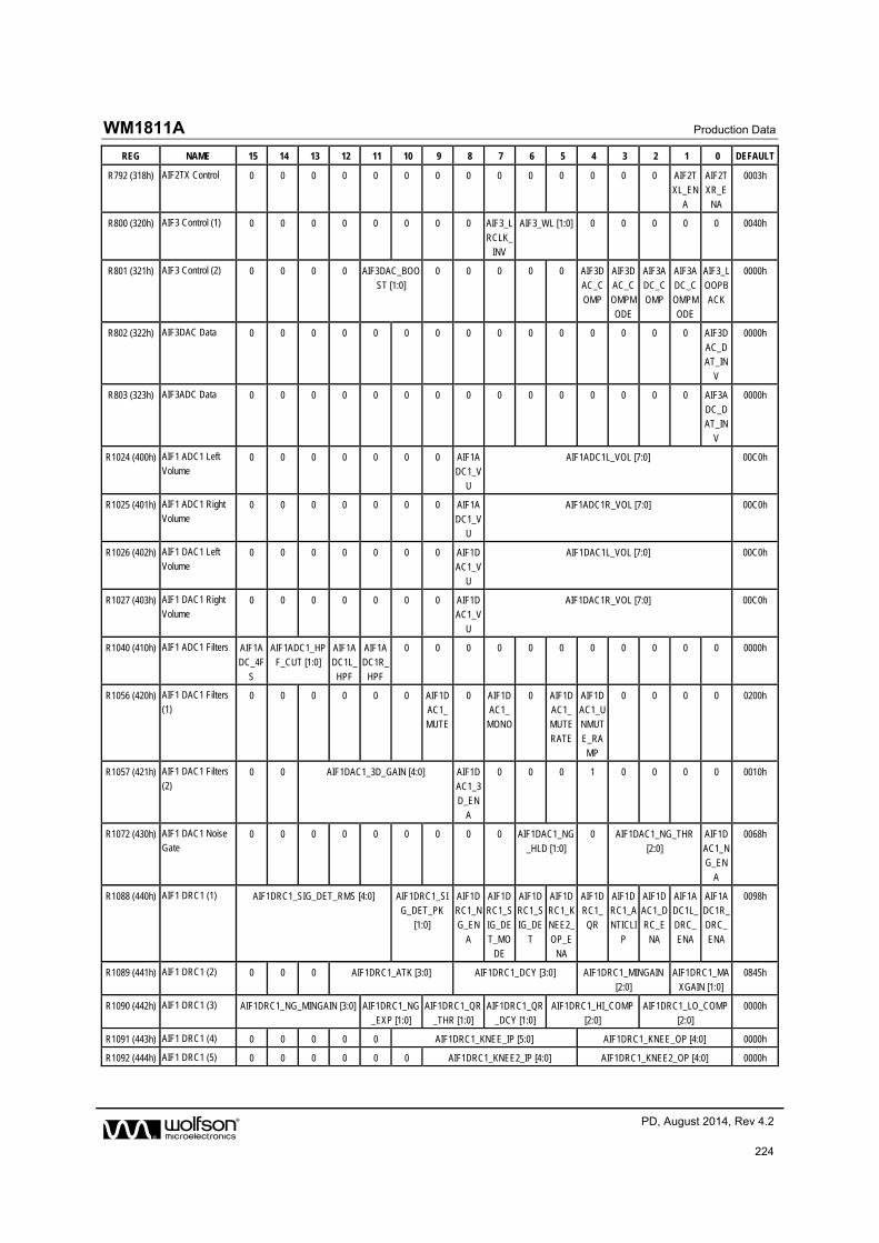
WM1811A Production Data
w PD, August 2014, Rev 4.2
224
REG NAME 15 14 13 12 11 10 9 8 7 6 5 4 3 2 1 0 DEFAULT
R792 (318h) AIF2TX Control 0 0 0 0 0 0 0 0 0 0 0 0 0 0 AIF2T
XL_ENA
AIF2T
XR_ENA
0003h
R800 (320h) AIF3 Control (1) 0 0 0 0 0 0 0 0 AIF3_L
RCLK_INV
AIF3_WL [1:0] 0 0 0 0 0 0040h
R801 (321h) AIF3 Control (2) 0 0 0 0 AIF3DAC_BOOST [1:0]
0 0 0 0 0 AIF3DAC_C
OMP
AIF3DAC_C
OMPMODE
AIF3ADC_C
OMP
AIF3ADC_C
OMPMODE
AIF3_LOOPB
ACK
0000h
R802 (322h) AIF3DAC Data 0 0 0 0 0 0 0 0 0 0 0 0 0 0 0 AIF3D
AC_DAT_IN
V
0000h
R803 (323h) AIF3ADC Data 0 0 0 0 0 0 0 0 0 0 0 0 0 0 0 AIF3A
DC_DAT_IN
V
0000h
R1024 (400h) AIF1 ADC1 Left Volume
0 0 0 0 0 0 0 AIF1ADC1_V
U
AIF1ADC1L_VOL [7:0] 00C0h
R1025 (401h) AIF1 ADC1 Right Volume
0 0 0 0 0 0 0 AIF1A
DC1_VU
AIF1ADC1R_VOL [7:0] 00C0h
R1026 (402h) AIF1 DAC1 Left
Volume 0 0 0 0 0 0 0 AIF1D
AC1_VU
AIF1DAC1L_VOL [7:0] 00C0h
R1027 (403h) AIF1 DAC1 Right
Volume 0 0 0 0 0 0 0 AIF1D
AC1_V
U
AIF1DAC1R_VOL [7:0] 00C0h
R1040 (410h) AIF1 ADC1 Filters AIF1ADC_4F
S
AIF1ADC1_HPF_CUT [1:0]
AIF1ADC1L_
HPF
AIF1ADC1R_
HPF
0 0 0 0 0 0 0 0 0 0 0 0000h
R1056 (420h) AIF1 DAC1 Filters (1)
0 0 0 0 0 0 AIF1DAC1_MUTE
0 AIF1DAC1_
MONO
0 AIF1DAC1_MUTE
RATE
AIF1DAC1_UNMUT
E_RAMP
0 0 0 0 0200h
R1057 (421h) AIF1 DAC1 Filters
(2) 0 0 AIF1DAC1_3D_GAIN [4:0] AIF1D
AC1_3D_EN
A
0 0 0 1 0 0 0 0 0010h
R1072 (430h) AIF1 DAC1 Noise Gate
0 0 0 0 0 0 0 0 0 AIF1DAC1_NG
_HLD [1:0]
0 AIF1DAC1_NG_THR
[2:0]
AIF1D
AC1_NG_EN
A
0068h
R1088 (440h) AIF1 DRC1 (1) AIF1DRC1_SIG_DET_RMS [4:0] AIF1DRC1_SIG_DET_PK
[1:0]
AIF1DRC1_NG_EN
A
AIF1DRC1_SIG_DE
T_MODE
AIF1DRC1_SIG_DE
T
AIF1DRC1_KNEE2_
OP_ENA
AIF1DRC1_QR
AIF1DRC1_ANTICLI
P
AIF1DAC1_DRC_E
NA
AIF1ADC1L_DRC_
ENA
AIF1ADC1R_DRC_
ENA
0098h
R1089 (441h) AIF1 DRC1 (2) 0 0 0 AIF1DRC1_ATK [3:0] AIF1DRC1_DCY [3:0] AIF1DRC1_MINGAIN
[2:0]
AIF1DRC1_MA
XGAIN [1:0]
0845h
R1090 (442h) AIF1 DRC1 (3) AIF1DRC1_NG_MINGAIN [3:0] AIF1DRC1_NG_EXP [1:0]
AIF1DRC1_QR_THR [1:0]
AIF1DRC1_QR_DCY [1:0]
AIF1DRC1_HI_COMP [2:0]
AIF1DRC1_LO_COMP [2:0]
0000h
R1091 (443h) AIF1 DRC1 (4) 0 0 0 0 0 AIF1DRC1_KNEE_IP [5:0] AIF1DRC1_KNEE_OP [4:0] 0000h
R1092 (444h) AIF1 DRC1 (5) 0 0 0 0 0 0 AIF1DRC1_KNEE2_IP [4:0] AIF1DRC1_KNEE2_OP [4:0] 0000h

Production Data WM1811A
w PD, August 2014, Rev 4.2
225
REG NAME 15 14 13 12 11 10 9 8 7 6 5 4 3 2 1 0 DEFAULT
R1152 (480h) AIF1 DAC1 EQ Gains (1)
AIF1DAC1_EQ_B1_GAIN [4:0] AIF1DAC1_EQ_B2_GAIN [4:0] AIF1DAC1_EQ_B3_GAIN [4:0] AIF1DAC1_EQ_EN
A
6318h
R1153 (481h) AIF1 DAC1 EQ Gains (2)
AIF1DAC1_EQ_B4_GAIN [4:0] AIF1DAC1_EQ_B5_GAIN [4:0] 0 0 0 0 0 AIF1DAC1_E
Q_MODE
6300h
R1154 (482h) AIF1 DAC1 EQ
Band 1 A AIF1DAC1_EQ_B1_A [15:0] 0FCAh
R1155 (483h) AIF1 DAC1 EQ Band 1 B
AIF1DAC1_EQ_B1_B [15:0] 0400h
R1156 (484h) AIF1 DAC1 EQ Band 1 PG
AIF1DAC1_EQ_B1_PG [15:0] 00D8h
R1157 (485h) AIF1 DAC1 EQ
Band 2 A AIF1DAC1_EQ_B2_A [15:0] 1EB5h
R1158 (486h) AIF1 DAC1 EQ Band 2 B
AIF1DAC1_EQ_B2_B [15:0] F145h
R1159 (487h) AIF1 DAC1 EQ Band 2 C
AIF1DAC1_EQ_B2_C [15:0] 0B75h
R1160 (488h) AIF1 DAC1 EQ
Band 2 PG AIF1DAC1_EQ_B2_PG [15:0] 01C5h
R1161 (489h) AIF1 DAC1 EQ Band 3 A
AIF1DAC1_EQ_B3_A [15:0] 1C58h
R1162 (48Ah) AIF1 DAC1 EQ
Band 3 B AIF1DAC1_EQ_B3_B [15:0] F373h
R1163 (48Bh) AIF1 DAC1 EQ Band 3 C
AIF1DAC1_EQ_B3_C [15:0] 0A54h
R1164 (48Ch) AIF1 DAC1 EQ Band 3 PG
AIF1DAC1_EQ_B3_PG [15:0] 0558h
R1165 (48Dh) AIF1 DAC1 EQ
Band 4 A AIF1DAC1_EQ_B4_A [15:0] 168Eh
R1166 (48Eh) AIF1 DAC1 EQ Band 4 B
AIF1DAC1_EQ_B4_B [15:0] F829h
R1167 (48Fh) AIF1 DAC1 EQ
Band 4 C AIF1DAC1_EQ_B4_C [15:0] 07ADh
R1168 (490h) AIF1 DAC1 EQ Band 4 PG
AIF1DAC1_EQ_B4_PG [15:0] 1103h
R1169 (491h) AIF1 DAC1 EQ Band 5 A
AIF1DAC1_EQ_B5_A [15:0] 0564h
R1170 (492h) AIF1 DAC1 EQ
Band 5 B AIF1DAC1_EQ_B5_B [15:0] 0559h
R1171 (493h) AIF1 DAC1 EQ Band 5 PG
AIF1DAC1_EQ_B5_PG [15:0] 4000h
R1172 (494h) AIF1 DAC1 EQ Band 1 C
AIF1DAC1_EQ_B1_C [15:0] 0000h
R1280 (500h) AIF2 ADC Left
Volume 0 0 0 0 0 0 0 AIF2A
DC_VU
AIF2ADCL_VOL [7:0] 00C0h
R1281 (501h) AIF2 ADC Right
Volume 0 0 0 0 0 0 0 AIF2A
DC_V
U
AIF2ADCR_VOL [7:0] 00C0h
R1282 (502h) AIF2 DAC Left Volume
0 0 0 0 0 0 0 AIF2DAC_V
U
AIF2DACL_VOL [7:0] 00C0h
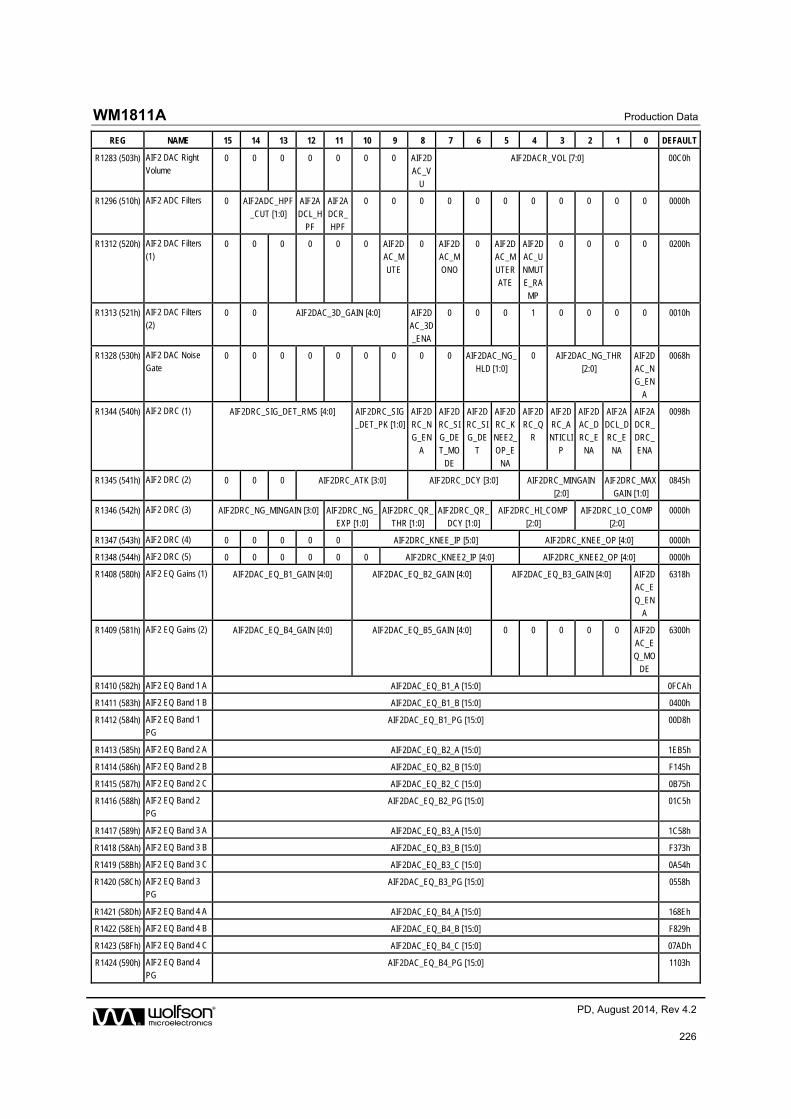
WM1811A Production Data
w PD, August 2014, Rev 4.2
226
REG NAME 15 14 13 12 11 10 9 8 7 6 5 4 3 2 1 0 DEFAULT
R1283 (503h) AIF2 DAC Right Volume
0 0 0 0 0 0 0 AIF2D
AC_VU
AIF2DACR_VOL [7:0] 00C0h
R1296 (510h) AIF2 ADC Filters 0 AIF2ADC_HPF
_CUT [1:0]
AIF2A
DCL_HPF
AIF2A
DCR_HPF
0 0 0 0 0 0 0 0 0 0 0 0000h
R1312 (520h) AIF2 DAC Filters
(1) 0 0 0 0 0 0 AIF2D
AC_M
UTE
0 AIF2DAC_M
ONO
0 AIF2DAC_M
UTERATE
AIF2DAC_U
NMUTE_RA
MP
0 0 0 0 0200h
R1313 (521h) AIF2 DAC Filters (2)
0 0 AIF2DAC_3D_GAIN [4:0] AIF2DAC_3D_ENA
0 0 0 1 0 0 0 0 0010h
R1328 (530h) AIF2 DAC Noise Gate
0 0 0 0 0 0 0 0 0 AIF2DAC_NG_
HLD [1:0]
0 AIF2DAC_NG_THR
[2:0]
AIF2D
AC_NG_EN
A
0068h
R1344 (540h) AIF2 DRC (1) AIF2DRC_SIG_DET_RMS [4:0] AIF2DRC_SIG_DET_PK [1:0]
AIF2DRC_NG_EN
A
AIF2DRC_SIG_DE
T_MODE
AIF2DRC_SIG_DE
T
AIF2DRC_KNEE2_
OP_ENA
AIF2DRC_Q
R
AIF2DRC_ANTICLI
P
AIF2DAC_DRC_E
NA
AIF2ADCL_DRC_E
NA
AIF2ADCR_DRC_
ENA
0098h
R1345 (541h) AIF2 DRC (2) 0 0 0 AIF2DRC_ATK [3:0] AIF2DRC_DCY [3:0] AIF2DRC_MINGAIN
[2:0]
AIF2DRC_MAX
GAIN [1:0]
0845h
R1346 (542h) AIF2 DRC (3) AIF2DRC_NG_MINGAIN [3:0] AIF2DRC_NG_EXP [1:0]
AIF2DRC_QR_THR [1:0]
AIF2DRC_QR_DCY [1:0]
AIF2DRC_HI_COMP [2:0]
AIF2DRC_LO_COMP [2:0]
0000h
R1347 (543h) AIF2 DRC (4) 0 0 0 0 0 AIF2DRC_KNEE_IP [5:0] AIF2DRC_KNEE_OP [4:0] 0000h
R1348 (544h) AIF2 DRC (5) 0 0 0 0 0 0 AIF2DRC_KNEE2_IP [4:0] AIF2DRC_KNEE2_OP [4:0] 0000h
R1408 (580h) AIF2 EQ Gains (1) AIF2DAC_EQ_B1_GAIN [4:0] AIF2DAC_EQ_B2_GAIN [4:0] AIF2DAC_EQ_B3_GAIN [4:0] AIF2DAC_E
Q_ENA
6318h
R1409 (581h) AIF2 EQ Gains (2) AIF2DAC_EQ_B4_GAIN [4:0] AIF2DAC_EQ_B5_GAIN [4:0] 0 0 0 0 0 AIF2D
AC_EQ_MO
DE
6300h
R1410 (582h) AIF2 EQ Band 1 A AIF2DAC_EQ_B1_A [15:0] 0FCAh
R1411 (583h) AIF2 EQ Band 1 B AIF2DAC_EQ_B1_B [15:0] 0400h
R1412 (584h) AIF2 EQ Band 1 PG
AIF2DAC_EQ_B1_PG [15:0] 00D8h
R1413 (585h) AIF2 EQ Band 2 A AIF2DAC_EQ_B2_A [15:0] 1EB5h
R1414 (586h) AIF2 EQ Band 2 B AIF2DAC_EQ_B2_B [15:0] F145h
R1415 (587h) AIF2 EQ Band 2 C AIF2DAC_EQ_B2_C [15:0] 0B75h
R1416 (588h) AIF2 EQ Band 2 PG
AIF2DAC_EQ_B2_PG [15:0] 01C5h
R1417 (589h) AIF2 EQ Band 3 A AIF2DAC_EQ_B3_A [15:0] 1C58h
R1418 (58Ah) AIF2 EQ Band 3 B AIF2DAC_EQ_B3_B [15:0] F373h
R1419 (58Bh) AIF2 EQ Band 3 C AIF2DAC_EQ_B3_C [15:0] 0A54h
R1420 (58Ch) AIF2 EQ Band 3
PG AIF2DAC_EQ_B3_PG [15:0] 0558h
R1421 (58Dh) AIF2 EQ Band 4 A AIF2DAC_EQ_B4_A [15:0] 168Eh
R1422 (58Eh) AIF2 EQ Band 4 B AIF2DAC_EQ_B4_B [15:0] F829h
R1423 (58Fh) AIF2 EQ Band 4 C AIF2DAC_EQ_B4_C [15:0] 07ADh
R1424 (590h) AIF2 EQ Band 4
PG AIF2DAC_EQ_B4_PG [15:0] 1103h

Production Data WM1811A
w PD, August 2014, Rev 4.2
227
REG NAME 15 14 13 12 11 10 9 8 7 6 5 4 3 2 1 0 DEFAULT
R1425 (591h) AIF2 EQ Band 5 A AIF2DAC_EQ_B5_A [15:0] 0564h
R1426 (592h) AIF2 EQ Band 5 B AIF2DAC_EQ_B5_B [15:0] 0559h
R1427 (593h) AIF2 EQ Band 5 PG
AIF2DAC_EQ_B5_PG [15:0] 4000h
R1428 (594h) AIF2 EQ Band 1 C AIF2DAC_EQ_B1_C [15:0] 0000h
R1536 (600h) DAC1 Mixer Volumes
0 0 0 0 0 0 0 ADCR_DAC1_VOL [3:0] 0 ADCL_DAC1_VOL [3:0] 0000h
R1537 (601h) DAC1 Left Mixer
Routing 0 0 0 0 0 0 0 0 0 0 ADCR
_TO_DAC1L
ADCL_
TO_DAC1L
0 AIF2D
ACL_TO_DAC1L
0 AIF1D
AC1L_TO_DAC1L
0000h
R1538 (602h) DAC1 Right Mixer Routing
0 0 0 0 0 0 0 0 0 0 ADCR
_TO_DAC1R
ADCL_
TO_DAC1R
0 AIF2D
ACR_TO_D
AC1R
0 AIF1D
AC1R_TO_D
AC1R
0000h
R1539 (603h) AIF2ADC Mixer Volumes
0 0 0 0 0 0 0 ADCR_AIF2ADC_VOL [3:0] 0 ADCL_AIF2ADC_VOL [3:0] 0000h
R1540 (604h) AIF2ADC Left
Mixer Routing 0 0 0 0 0 0 0 0 0 0 ADCR
_TO_A
IF2ADCL
ADCL_TO_AI
F2ADCL
0 AIF2DACL_T
O_AIF2ADCL
0 AIF1DAC1L_
TO_AIF2AD
CL
0000h
R1541 (605h) AIF2ADC Right Mixer Routing
0 0 0 0 0 0 0 0 0 0 ADCR_TO_AIF2AD
CR
ADCL_TO_AIF2AD
CR
0 AIF2DACR_TO_AI
F2ADCR
0 AIF1DAC1R_TO_AI
F2ADCR
0000h
R1542 (606h) AIF1 ADC1 Left
Mixer Routing 0 0 0 0 0 0 0 0 0 0 0 0 0 0 ADC1L
_TO_AIF1ADC1L
AIF2D
ACL_TO_AIF1ADC1
L
0000h
R1543 (607h) AIF1 ADC1 Right Mixer Routing
0 0 0 0 0 0 0 0 0 0 0 0 0 0 ADC1R_TO_
AIF1ADC1R
AIF2DACR_
TO_AIF1ADC1R
0000h
R1552 (610h) DAC1 Left Volume 0 0 0 0 0 0 DAC1L
_MUTE
DAC1_
VU
DAC1L_VOL [7:0] 02C0h
R1553 (611h) DAC1 Right
Volume 0 0 0 0 0 0 DAC1
R_MUTE
DAC1_
VU
DAC1R_VOL [7:0] 02C0h
R1554 (612h) AIF2TX Left
Volume 0 0 0 0 0 0 AIF2T
XL_M
UTE
AIF2TX_VU
AIF2TXL_VOL [7:0] 02C0h
R1555 (613h) AIF2TX Right Volume
0 0 0 0 0 0 AIF2TXR_M
UTE
AIF2TX_VU
AIF2TXR_VOL [7:0] 02C0h
R1556 (614h) DAC Softmute 0 0 0 0 0 0 0 0 0 0 0 0 0 0 DAC_SOFTMUTE
MODE
DAC_MUTERATE
0000h
R1568 (620h) Oversampling 0 0 0 0 0 0 0 0 0 0 0 0 0 0 ADC_OSR1
28
DAC_OSR1
28
0002h
R1569 (621h) Sidetone 0 0 0 0 0 0 ST_HPF_CUT [2:0] ST_HPF
0 0 0 0 0 0 0000h

WM1811A Production Data
w PD, August 2014, Rev 4.2
228
REG NAME 15 14 13 12 11 10 9 8 7 6 5 4 3 2 1 0 DEFAULT
R1792 (700h) GPIO 1 GP1_
DIR
GP1_P
U
GP1_P
D
0 0 GP1_P
OL
GP1_
OP_CFG
GP1_
DB
0 GP1_L
VL
0 GP1_FN [4:0] 8100h
R1793 (701h) Pull Control
(MCLK2) 1 MCLK
2_PU
MCLK
2_PD
0 0 0 0 1 0 0 0 0 0 0 0 1 A101h
R1794 (702h) Pull Control (BCLK2)
1 BCLK2_PU
BCLK2_PD
0 0 0 0 1 0 0 0 0 0 0 0 1 A101h
R1795 (703h) Pull Control
(DACLRCLK2) 1 DACL
RCLK2
_PU
DACLRCLK2
_PD
0 0 0 0 1 0 0 0 0 0 0 0 1 A101h
R1796 (704h) Pull Control (DACDAT2)
1 DACDAT2_P
U
DACDAT2_P
D
0 0 0 0 1 0 0 0 0 0 0 0 1 A101h
R1797 (705h) JACKDET Ctrl 1 0 1 0 0 0 0 JACKDET_
DB
0 JACKDET_L
VL
0 0 0 0 0 1 A101h
R1799 (707h) GPIO 8 GP8_
DIR
GP8_P
U
GP8_P
D
0 0 GP8_P
OL
GP8_
OP_CFG
GP8_
DB
0 GP8_L
VL
0 GP8_FN [4:0] A101h
R1800 (708h) GPIO 9 GP9_
DIR
GP9_P
U
GP9_P
D
0 0 GP9_P
OL
GP9_
OP_CFG
GP9_
DB
0 GP9_L
VL
0 GP9_FN [4:0] A101h
R1801 (709h) GPIO 10 GP10_DIR
GP10_PU
GP10_PD
0 0 GP10_POL
GP10_OP_C
FG
GP10_DB
0 GP10_LVL
0 GP10_FN [4:0] A101h
R1802 (70Ah) GPIO 11 GP11_DIR
GP11_PU
GP11_PD
0 0 GP11_POL
GP11_OP_C
FG
GP11_DB
0 GP11_LVL
0 GP11_FN [4:0] A101h
R1824 (720h) Pull Control (1) 0 0 0 0 0 0 DMICDAT1_
PU
DMICDAT1_
PD
MCLK1_PU
MCLK1_PD
DACDAT1_P
U
DACDAT1_P
D
DACLRCLK1
_PU
DACLRCLK1
_PD
BCLK1_PU
BCLK1_PD
0000h
R1825 (721h) Pull Control (2) 0 0 0 0 0 0 0 ADDR
_PD
0 LDO2
ENA_PD
0 LDO1
ENA_PD
0 1 SPKM
ODE_PU
0 0156h
R1840 (730h) Interrupt Status 1 0 0 0 0 0 GP11_
EINT
GP10_
EINT
GP9_E
INT
GP8_E
INT
0 JACK
DET_EINT
0 0 0 0 GP1_E
INT
0000h
R1841 (731h) Interrupt Status 2 TEMP_WAR
N_EINT
DCS_DONE
_EINT
0 FIFOS_ERR_
EINT
AIF2DRC_SI
G_DET_EIN
T
0 AIF1DRC1_S
IG_DET_EIN
T
SRC2_LOCK
_EINT
SRC1_LOCK
_EINT
FLL2_LOCK
_EINT
FLL1_LOCK
_EINT
0 0 0 MICD_EINT
TEMP_SHU
T_EINT
0000h
R1842 (732h) Interrupt Raw Status 2
TEMP_WARN_STS
DCS_DONE_STS
0 FIFOS_ERR_
STS
AIF2DRC_SIG_DE
T_STS
0 AIF1DRC1_SIG_DE
T_STS
SRC2_LOCK_STS
SRC1_LOCK_STS
FLL2_LOCK_STS
FLL1_LOCK_STS
0 0 0 0 TEMP_SHUT_STS
0000h
R1848 (738h) Interrupt Status 1 Mask
0 0 0 0 0 IM_GP11_EI
NT
IM_GP10_EI
NT
IM_GP9_EIN
T
IM_GP8_EIN
T
1 IM_JACKDE
T_EINT
1 1 1 1 IM_GP1_EIN
T
07FFh
R1849 (739h) Interrupt Status 2
Mask IM_TEMP_W
ARN_EINT
IM_DCS_DO
NE_EINT
0 IM_FIFOS_E
RR_EINT
IM_AIF2DRC_
SIG_DET_EI
NT
0 IM_AIF1DRC1
_SIG_DET_E
INT
IM_SRC2_LO
CK_EINT
IM_SRC1_LO
CK_EINT
IM_FLL2_LO
CK_EINT
IM_FLL1_LO
CK_EINT
0 1 1 IM_MICD_EI
NT
IM_TEMP_S
HUT_EINT
DBEFh
R1856 (740h) Interrupt Control 0 0 0 0 0 0 0 0 0 0 0 0 0 0 0 IM_IRQ
0000h

Production Data WM1811A
w PD, August 2014, Rev 4.2
229
REG NAME 15 14 13 12 11 10 9 8 7 6 5 4 3 2 1 0 DEFAULT
R1864 (748h) IRQ Debounce 0 0 0 0 0 0 0 0 0 0 TEMP_WARN_DB
1 1 1 1 TEMP_SHUT_DB
003Fh

WM1811A Production Data
w PD, August 2014, Rev 4.2
230
REGISTER BITS BY ADDRESS
REGISTER
ADDRESS
BIT LABEL DEFAULT DESCRIPTION
R0 (00h) Software
Reset
15:0 SW_RESET [15:0]
0001_1000_0001_0001
Writing to this register resets all registers to their default state.
Reading from this register will indicate device ID 1811h.
Register 00h Software Reset
REGISTER
ADDRESS
BIT LABEL DEFAULT DESCRIPTION
R1 (01h) Power
Management (1)
13 SPKOUTR_ENA 0 SPKMIXR Mixer, SPKRVOL PGA and SPKOUTR Output Enable
0 = Disabled
1 = Enabled
12 SPKOUTL_ENA 0 SPKMIXL Mixer, SPKLVOL PGA and SPKOUTL Output Enable
0 = Disabled
1 = Enabled
11 HPOUT2_ENA 0 HPOUT2 Output Stage Enable
0 = Disabled
1 = Enabled
9 HPOUT1L_ENA 0 Enables HPOUT1L input stage
0 = Disabled
1 = Enabled
For normal operation, this bit should be set as the first step of the HPOUT1L Enable sequence.
8 HPOUT1R_ENA 0 Enables HPOUT1R input stage
0 = Disabled
1 = Enabled
For normal operation, this bit should be set as the first step of the HPOUT1R Enable sequence.
5 MICB2_ENA 0 Microphone Bias 2 Enable
0 = Disabled
1 = Enabled
4 MICB1_ENA 0 Microphone Bias 1 Enable
0 = Disabled
1 = Enabled
2:1 VMID_SEL [1:0] 00 VMID Divider Enable and Select
00 = VMID disabled (for OFF mode)
01 = 2 x 40k divider (for normal operation)
10 = 2 x 240k divider (for low power standby)
11 = Reserved
0 BIAS_ENA 0 Enables the Normal bias current generator (for all analogue functions)
0 = Disabled
1 = Enabled
Register 01h Power Management (1)
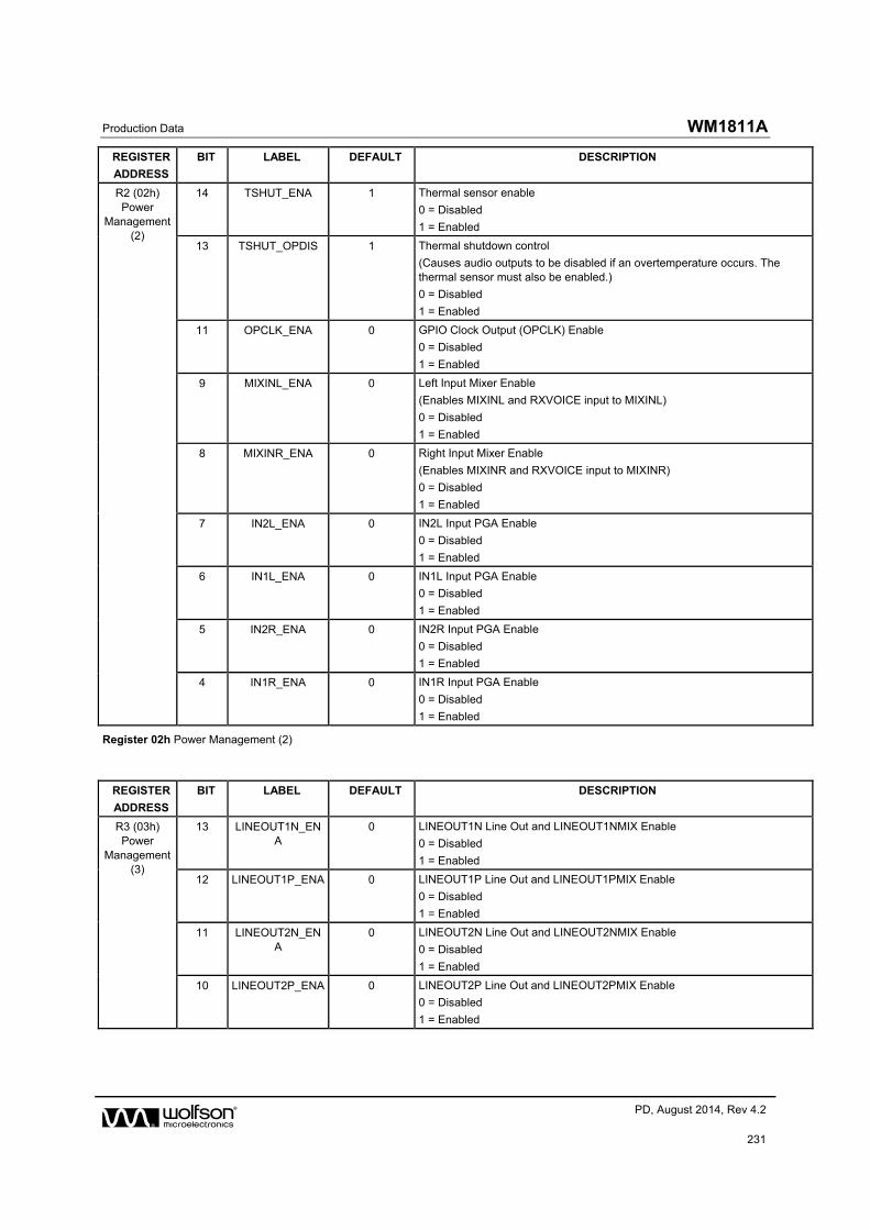
Production Data WM1811A
w PD, August 2014, Rev 4.2
231
REGISTER
ADDRESS
BIT LABEL DEFAULT DESCRIPTION
R2 (02h) Power
Management (2)
14 TSHUT_ENA 1 Thermal sensor enable
0 = Disabled
1 = Enabled
13 TSHUT_OPDIS 1 Thermal shutdown control
(Causes audio outputs to be disabled if an overtemperature occurs. The thermal sensor must also be enabled.)
0 = Disabled
1 = Enabled
11 OPCLK_ENA 0 GPIO Clock Output (OPCLK) Enable
0 = Disabled
1 = Enabled
9 MIXINL_ENA 0 Left Input Mixer Enable
(Enables MIXINL and RXVOICE input to MIXINL)
0 = Disabled
1 = Enabled
8 MIXINR_ENA 0 Right Input Mixer Enable
(Enables MIXINR and RXVOICE input to MIXINR)
0 = Disabled
1 = Enabled
7 IN2L_ENA 0 IN2L Input PGA Enable
0 = Disabled
1 = Enabled
6 IN1L_ENA 0 IN1L Input PGA Enable
0 = Disabled
1 = Enabled
5 IN2R_ENA 0 IN2R Input PGA Enable
0 = Disabled
1 = Enabled
4 IN1R_ENA 0 IN1R Input PGA Enable
0 = Disabled
1 = Enabled
Register 02h Power Management (2)
REGISTER
ADDRESS
BIT LABEL DEFAULT DESCRIPTION
R3 (03h) Power
Management (3)
13 LINEOUT1N_ENA
0 LINEOUT1N Line Out and LINEOUT1NMIX Enable
0 = Disabled
1 = Enabled
12 LINEOUT1P_ENA 0 LINEOUT1P Line Out and LINEOUT1PMIX Enable
0 = Disabled
1 = Enabled
11 LINEOUT2N_ENA
0 LINEOUT2N Line Out and LINEOUT2NMIX Enable
0 = Disabled
1 = Enabled
10 LINEOUT2P_ENA 0 LINEOUT2P Line Out and LINEOUT2PMIX Enable
0 = Disabled
1 = Enabled

WM1811A Production Data
w PD, August 2014, Rev 4.2
232
REGISTER
ADDRESS
BIT LABEL DEFAULT DESCRIPTION
9 SPKRVOL_ENA 0 SPKMIXR Mixer and SPKRVOL PGA Enable
0 = Disabled
1 = Enabled
Note that SPKMIXR and SPKRVOL are also enabled when SPKOUTR_ENA is set.
8 SPKLVOL_ENA 0 SPKMIXL Mixer and SPKLVOL PGA Enable
0 = Disabled
1 = Enabled
Note that SPKMIXL and SPKLVOL are also enabled when SPKOUTL_ENA is set.
7 MIXOUTLVOL_ENA
0 MIXOUTL Left Volume Control Enable
0 = Disabled
1 = Enabled
6 MIXOUTRVOL_ENA
0 MIXOUTR Right Volume Control Enable
0 = Disabled
1 = Enabled
5 MIXOUTL_ENA 0 MIXOUTL Left Output Mixer Enable
0 = Disabled
1 = Enabled
4 MIXOUTR_ENA 0 MIXOUTR Right Output Mixer Enable
0 = Disabled
1 = Enabled
Register 03h Power Management (3)
REGISTER
ADDRESS
BIT LABEL DEFAULT DESCRIPTION
R4 (04h) Power
Management (4)
13 AIF2ADCL_ENA 0 Enable AIF2ADC (Left) output path
0 = Disabled
1 = Enabled
This bit must be set for AIF2 or AIF3 output of the AIF2ADC (Left) signal.
12 AIF2ADCR_ENA 0 Enable AIF2ADC (Right) output path
0 = Disabled
1 = Enabled
This bit must be set for AIF2 or AIF3 output of the AIF2ADC (Left) signal.
9 AIF1ADC1L_ENA 0 Enable AIF1ADC (Left) output path
0 = Disabled
1 = Enabled
8 AIF1ADC1R_ENA 0 Enable AIF1ADC (Right) output path
0 = Disabled
1 = Enabled
3 DMIC1L_ENA 0 Digital microphone (DMICDAT) Left channel enable
0 = Disabled
1 = Enabled
2 DMIC1R_ENA 0 Digital microphone (DMICDAT) Right channel enable
0 = Disabled
1 = Enabled
1 ADCL_ENA 0 Left ADC Enable
0 = Disabled
1 = Enabled

Production Data WM1811A
w PD, August 2014, Rev 4.2
233
REGISTER
ADDRESS
BIT LABEL DEFAULT DESCRIPTION
0 ADCR_ENA 0 Right ADC Enable
0 = Disabled
1 = Enabled
Register 04h Power Management (4)
REGISTER
ADDRESS
BIT LABEL DEFAULT DESCRIPTION
R5 (05h) Power
Management (5)
13 AIF2DACL_ENA 0 Enable AIF2DAC (Left) input path
0 = Disabled
1 = Enabled
12 AIF2DACR_ENA 0 Enable AIF2DAC (Right) input path
0 = Disabled
1 = Enabled
9 AIF1DAC1L_ENA 0 Enable AIF1DAC (Left) input path
0 = Disabled
1 = Enabled
8 AIF1DAC1R_ENA 0 Enable AIF1DAC (Right) input path
0 = Disabled
1 = Enabled
1 DAC1L_ENA 0 Left DAC Enable
0 = Disabled
1 = Enabled
0 DAC1R_ENA 0 Right DAC Enable
0 = Disabled
1 = Enabled
Register 05h Power Management (5)
REGISTER
ADDRESS
BIT LABEL DEFAULT DESCRIPTION
R6 (06h) Power
Management (6)
10:9 AIF3ADC_SRC [1:0]
00 AIF3 Mono PCM output source select 00 = None 01 = AIF2ADC (Left) output path 10 = AIF2ADC (Right) output path 11 = Reserved
8:7 AIF2DAC_SRC [1:0]
00 AIF2 input path select
00 = Left and Right inputs from AIF2
01 = Left input from AIF2; Right input from AIF3
10 = Left input from AIF3; Right input from AIF2
11 = Reserved
5 AIF3_TRI 0 AIF3 Audio Interface tri-state
0 = AIF3 pins operate normally
1 = Tri-state all AIF3 interface pins
Note that pins not configured as AIF3 functions are not affected by this register.
4:3 AIF3_ADCDAT_SRC [1:0]
00 GPIO9/ADCDAT3 Source select
00 = AIF1 ADCDAT1
01 = AIF2 ADCDAT2
10 = DACDAT2
11 = AIF3 Mono PCM output
Note that GPIO9 must be configured as ADCDAT3.

WM1811A Production Data
w PD, August 2014, Rev 4.2
234
REGISTER
ADDRESS
BIT LABEL DEFAULT DESCRIPTION
2 AIF2_ADCDAT_SRC
0 ADCDAT2 Source select
0 = AIF2 ADCDAT2
1 = GPIO8/DACDAT3
For selection 1, the GPIO8 pin must also be configured as DACDAT3.
1 AIF2_DACDAT_SRC
0 AIF2 DACDAT Source select
0 = DACDAT2
1 = GPIO8/DACDAT3
For selection 1, the GPIO8 pin must also be configured as DACDAT3.
0 AIF1_DACDAT_SRC
0 AIF1 DACDAT Source select
0 = DACDAT1
1 = GPIO8/DACDAT3
Note that, for selection 1, the GPIO8 pin must be configured as DACDAT3.
Register 06h Power Management (6)
REGISTER
ADDRESS
BIT LABEL DEFAULT DESCRIPTION
R21 (15h) Input Mixer
(1)
8 IN1RP_MIXINR_BOOST
0 IN1RP Pin (PGA Bypass) to MIXINR Gain Boost.
This bit selects the maximum gain setting of the IN1RP_MIXINR_VOL register.
0 = Maximum gain is +6dB
1 = Maximum gain is +15dB
7 IN1LP_MIXINL_BOOST
0 IN1LP Pin (PGA Bypass) to MIXINL Gain Boost.
This bit selects the maximum gain setting of the IN1LP_MIXINL_VOL register.
0 = Maximum gain is +6dB
1 = Maximum gain is +15dB
6 INPUTS_CLAMP 0 Input pad VMID clamp
0 = Clamp de-activated
1 = Clamp activated
Register 15h Input Mixer (1)
REGISTER
ADDRESS
BIT LABEL DEFAULT DESCRIPTION
R24 (18h) Left Line Input 1&2 Volume
8 IN1_VU 0 Input PGA Volume Update
Writing a 1 to this bit will cause IN1L and IN1R input PGA volumes to be updated simultaneously
7 IN1L_MUTE 1 IN1L PGA Mute
0 = Disable Mute
1 = Enable Mute
6 IN1L_ZC 0 IN1L PGA Zero Cross Detector
0 = Change gain immediately
1 = Change gain on zero cross only
4:0 IN1L_VOL [4:0] 0_1011 IN1L Volume
-16.5dB to +30dB in 1.5dB steps
Register 18h Left Line Input 1&2 Volume

Production Data WM1811A
w PD, August 2014, Rev 4.2
235
REGISTER
ADDRESS
BIT LABEL DEFAULT DESCRIPTION
R25 (19h) Left Line Input 3&4 Volume
8 IN2_VU 0 Input PGA Volume Update
Writing a 1 to this bit will cause IN2L and IN2R input PGA volumes to be updated simultaneously
7 IN2L_MUTE 1 IN2L PGA Mute
0 = Disable Mute
1 = Enable Mute
6 IN2L_ZC 0 IN2L PGA Zero Cross Detector
0 = Change gain immediately
1 = Change gain on zero cross only
4:0 IN2L_VOL [4:0] 0_1011 IN2L Volume
-16.5dB to +30dB in 1.5dB steps
Register 19h Left Line Input 3&4 Volume
REGISTER
ADDRESS
BIT LABEL DEFAULT DESCRIPTION
R26 (1Ah) Right Line Input 1&2 Volume
8 IN1_VU 0 Input PGA Volume Update
Writing a 1 to this bit will cause IN1L and IN1R input PGA volumes to be updated simultaneously
7 IN1R_MUTE 1 IN1R PGA Mute
0 = Disable Mute
1 = Enable Mute
6 IN1R_ZC 0 IN1R PGA Zero Cross Detector
0 = Change gain immediately
1 = Change gain on zero cross only
4:0 IN1R_VOL [4:0] 0_1011 IN1R Volume
-16.5dB to +30dB in 1.5dB steps
Register 1Ah Right Line Input 1&2 Volume
REGISTER
ADDRESS
BIT LABEL DEFAULT DESCRIPTION
R27 (1Bh) Right Line Input 3&4 Volume
8 IN2_VU 0 Input PGA Volume Update
Writing a 1 to this bit will cause IN2L and IN2R input PGA volumes to be updated simultaneously
7 IN2R_MUTE 1 IN2R PGA Mute
0 = Disable Mute
1 = Enable Mute
6 IN2R_ZC 0 IN2R PGA Zero Cross Detector
0 = Change gain immediately
1 = Change gain on zero cross only
4:0 IN2R_VOL [4:0] 0_1011 IN2R Volume
-16.5dB to +30dB in 1.5dB steps
Register 1Bh Right Line Input 3&4 Volume

WM1811A Production Data
w PD, August 2014, Rev 4.2
236
REGISTER
ADDRESS
BIT LABEL DEFAULT DESCRIPTION
R28 (1Ch) Left Output
Volume
8 HPOUT1_VU 0 Headphone Output PGA Volume Update
Writing a 1 to this bit will update HPOUT1LVOL and HPOUT1RVOL volumes simultaneously.
7 HPOUT1L_ZC 0 HPOUT1LVOL (Left Headphone Output PGA) Zero Cross Enable
0 = Zero cross disabled
1 = Zero cross enabled
6 HPOUT1L_MUTE_N
1 HPOUT1LVOL (Left Headphone Output PGA) Mute
0 = Mute
1 = Un-mute
5:0 HPOUT1L_VOL [5:0]
10_1101 HPOUT1LVOL (Left Headphone Output PGA) Volume
-57dB to +6dB in 1dB steps
00_0000 = -57dB
00_0001 = -56dB
… (1dB steps)
11_1111 = +6dB
Register 1Ch Left Output Volume
REGISTER
ADDRESS
BIT LABEL DEFAULT DESCRIPTION
R29 (1Dh) Right Output
Volume
8 HPOUT1_VU 0 Headphone Output PGA Volume Update
Writing a 1 to this bit will update HPOUT1LVOL and HPOUT1RVOL volumes simultaneously.
7 HPOUT1R_ZC 0 HPOUT1RVOL (Right Headphone Output PGA) Zero Cross Enable
0 = Zero cross disabled
1 = Zero cross enabled
6 HPOUT1R_MUTE_N
1 HPOUT1RVOL (Right Headphone Output PGA) Mute
0 = Mute
1 = Un-mute
5:0 HPOUT1R_VOL [5:0]
10_1101 HPOUT1RVOL (Right Headphone Output PGA) Volume
-57dB to +6dB in 1dB steps
00_0000 = -57dB
00_0001 = -56dB
… (1dB steps)
11_1111 = +6dB
Register 1Dh Right Output Volume
REGISTER
ADDRESS
BIT LABEL DEFAULT DESCRIPTION
R30 (1Eh) Line Outputs
Volume
6 LINEOUT1N_MUTE
1 LINEOUT1N Line Output Mute
0 = Un-mute
1 = Mute
5 LINEOUT1P_MUTE
1 LINEOUT1P Line Output Mute
0 = Un-mute
1 = Mute
4 LINEOUT1_VOL 0 LINEOUT1 Line Output Volume
0 = 0dB
1 = -6dB
Applies to both LINEOUT1N and LINEOUT1P

Production Data WM1811A
w PD, August 2014, Rev 4.2
237
REGISTER
ADDRESS
BIT LABEL DEFAULT DESCRIPTION
2 LINEOUT2N_MUTE
1 LINEOUT2N Line Output Mute
0 = Un-mute
1 = Mute
1 LINEOUT2P_MUTE
1 LINEOUT2P Line Output Mute
0 = Un-mute
1 = Mute
0 LINEOUT2_VOL 0 LINEOUT2 Line Output Volume
0 = 0dB
1 = -6dB
Applies to both LINEOUT2N and LINEOUT2P
Register 1Eh Line Outputs Volume
REGISTER
ADDRESS
BIT LABEL DEFAULT DESCRIPTION
R31 (1Fh) HPOUT2 Volume
5 HPOUT2_MUTE 1 HPOUT2 (Earpiece Driver) Mute
0 = Mute
1 = Un-mute
4 HPOUT2_VOL 0 HPOUT2 (Earpiece Driver) Volume
0 = 0dB
1 = -6dB
Register 1Fh HPOUT2 Volume
REGISTER
ADDRESS
BIT LABEL DEFAULT DESCRIPTION
R32 (20h) Left OPGA
Volume
8 MIXOUT_VU 0 Mixer Output PGA Volume Update
Writing a 1 to this bit will update MIXOUTLVOL and MIXOUTRVOL volumes simultaneously.
7 MIXOUTL_ZC 0 MIXOUTLVOL (Left Mixer Output PGA) Zero Cross Enable
0 = Zero cross disabled
1 = Zero cross enabled
6 MIXOUTL_MUTE_N
1 MIXOUTLVOL (Left Mixer Output PGA) Mute
0 = Mute
1 = Un-mute
5:0 MIXOUTL_VOL [5:0]
11_1001 MIXOUTLVOL (Left Mixer Output PGA) Volume
-57dB to +6dB in 1dB steps
00_0000 = -57dB
00_0001 = -56dB
… (1dB steps)
11_1111 = +6dB
Register 20h Left OPGA Volume

WM1811A Production Data
w PD, August 2014, Rev 4.2
238
REGISTER
ADDRESS
BIT LABEL DEFAULT DESCRIPTION
R33 (21h) Right OPGA
Volume
8 MIXOUT_VU 0 Mixer Output PGA Volume Update
Writing a 1 to this bit will update MIXOUTLVOL and MIXOUTRVOL volumes simultaneously.
7 MIXOUTR_ZC 0 MIXOUTRVOL (Right Mixer Output PGA) Zero Cross Enable
0 = Zero cross disabled
1 = Zero cross enabled
6 MIXOUTR_MUTE_N
1 MIXOUTLVOL (Right Mixer Output PGA) Mute
0 = Mute
1 = Un-mute
5:0 MIXOUTR_VOL [5:0]
11_1001 MIXOUTRVOL (Right Mixer Output PGA) Volume
-57dB to +6dB in 1dB steps
00_0000 = -57dB
00_0001 = -56dB
… (1dB steps)
11_1111 = +6dB
Register 21h Right OPGA Volume
REGISTER
ADDRESS
BIT LABEL DEFAULT DESCRIPTION
R34 (22h) SPKMIXL
Attenuation
5 MIXINL_SPKMIXL_VOL
0 MIXINL (Left ADC bypass) to SPKMIXL Fine Volume Control
0 = 0dB
1 = -6dB
4 IN1LP_SPKMIXL_VOL
0 IN1LP to SPKMIXL Fine Volume Control
0 = 0dB
1 = -6dB
3 MIXOUTL_SPKMIXL_VOL
0 Left Mixer Output to SPKMIXL Fine Volume Control
0 = 0dB
1 = -6dB
2 DAC1L_SPKMIXL_VOL
0 Left DAC to SPKMIXL Fine Volume Control
0 = 0dB
1 = -6dB
1:0 SPKMIXL_VOL [1:0]
11 Left Speaker Mixer Volume Control
00 = 0dB
01 = Reserved
10 = Reserved
11 = Mute
Register 22h SPKMIXL Attenuation
REGISTER
ADDRESS
BIT LABEL DEFAULT DESCRIPTION
R35 (23h) SPKMIXR
Attenuation
5 MIXINR_SPKMIXR_VOL
0 MIXINR (Right ADC bypass) to SPKMIXR Fine Volume Control
0 = 0dB
1 = -6dB
4 IN1RP_SPKMIXR_VOL
0 IN1RP to SPKMIXR Fine Volume Control
0 = 0dB
1 = -6dB
3 MIXOUTR_SPKMIXR_VOL
0 Right Mixer Output to SPKMIXR Fine Volume Control
0 = 0dB
1 = -6dB

Production Data WM1811A
w PD, August 2014, Rev 4.2
239
REGISTER
ADDRESS
BIT LABEL DEFAULT DESCRIPTION
2 DAC1R_SPKMIXR_VOL
0 Right DAC to SPKMIXR Fine Volume Control
0 = 0dB
1 = -6dB
1:0 SPKMIXR_VOL [1:0]
11 Right Speaker Mixer Volume Control
00 = 0dB
01 = Reserved
10 = Reserved
11 = Mute
Register 23h SPKMIXR Attenuation
REGISTER
ADDRESS
BIT LABEL DEFAULT DESCRIPTION
R36 (24h) SPKOUT
Mixers
4 SPKMIXL_TO_SPKOUTL
1 SPKMIXL Left Speaker Mixer to Left Speaker Mute
0 = Mute
1 = Un-mute
3 SPKMIXR_TO_SPKOUTL
0 SPKMIXR Right Speaker Mixer to Left Speaker Mute
0 = Mute
1 = Un-mute
1 SPKMIXL_TO_SPKOUTR
0 SPKMIXL Left Speaker Mixer to Right Speaker Mute
0 = Mute
1 = Un-mute
0 SPKMIXR_TO_SPKOUTR
1 SPKMIXR Right Speaker Mixer to Right Speaker Mute
0 = Mute
1 = Un-mute
Register 24h SPKOUT Mixers
REGISTER
ADDRESS
BIT LABEL DEFAULT DESCRIPTION
R37 (25h) ClassD
6 Reserved 1 Reserved - do not change
5:3 SPKOUTL_BOOST [2:0]
000 Left Speaker Gain Boost
000 = 1.00x boost (+0dB)
001 = 1.19x boost (+1.5dB)
010 = 1.41x boost (+3.0dB)
011 = 1.68x boost (+4.5dB)
100 = 2.00x boost (+6.0dB)
101 = 2.37x boost (+7.5dB)
110 = 2.81x boost (+9.0dB)
111 = 3.98x boost (+12.0dB)
2:0 SPKOUTR_BOOST [2:0]
000 Right Speaker Gain Boost
000 = 1.00x boost (+0dB)
001 = 1.19x boost (+1.5dB)
010 = 1.41x boost (+3.0dB)
011 = 1.68x boost (+4.5dB)
100 = 2.00x boost (+6.0dB)
101 = 2.37x boost (+7.5dB)
110 = 2.81x boost (+9.0dB)
111 = 3.98x boost (+12.0dB)
Register 25h ClassD

WM1811A Production Data
w PD, August 2014, Rev 4.2
240
REGISTER
ADDRESS
BIT LABEL DEFAULT DESCRIPTION
R38 (26h) Speaker
Volume Left
8 SPKOUT_VU 0 Speaker Output PGA Volume Update
Writing a 1 to this bit will update SPKLVOL and SPKRVOL volumes simultaneously.
7 SPKOUTL_ZC 0 SPKLVOL (Left Speaker Output PGA) Zero Cross Enable
0 = Zero cross disabled
1 = Zero cross enabled
6 SPKOUTL_MUTE_N
1 SPKLVOL (Left Speaker Output PGA) Mute
0 = Mute
1 = Un-mute
5:0 SPKOUTL_VOL [5:0]
11_1001 SPKLVOL (Left Speaker Output PGA) Volume
-57dB to +6dB in 1dB steps
00_0000 = -57dB
00_0001 = -56dB
… (1dB steps)
11_1111 = +6dB
Register 26h Speaker Volume Left
REGISTER
ADDRESS
BIT LABEL DEFAULT DESCRIPTION
R39 (27h) Speaker
Volume Right
8 SPKOUT_VU 0 Speaker Output PGA Volume Update
Writing a 1 to this bit will update SPKLVOL and SPKRVOL volumes simultaneously.
7 SPKOUTR_ZC 0 SPKRVOL (Right Speaker Output PGA) Zero Cross Enable
0 = Zero cross disabled
1 = Zero cross enabled
6 SPKOUTR_MUTE_N
1 SPKRVOL (Right Speaker Output PGA) Mute
0 = Mute
1 = Un-mute
5:0 SPKOUTR_VOL [5:0]
11_1001 SPKRVOL (Right Speaker Output PGA) Volume
-57dB to +6dB in 1dB steps
00_0000 = -57dB
00_0001 = -56dB
… (1dB steps)
11_1111 = +6dB
Register 27h Speaker Volume Right
REGISTER
ADDRESS
BIT LABEL DEFAULT DESCRIPTION
R40 (28h) Input Mixer
(2)
7 IN2LP_TO_IN2L 0 IN2L PGA Non-Inverting Input Select
0 = Connected to VMID
1 = Connected to IN2LP
Note that VMID_BUF_ENA must be set when using IN2L connected to VMID.
6 IN2LN_TO_IN2L 0 IN2L PGA Inverting Input Select
0 = Not connected
1 = Connected to IN2LN
5 IN1LP_TO_IN1L 0 IN1L PGA Non-Inverting Input Select
0 = Connected to VMID
1 = Connected to IN1LP
Note that VMID_BUF_ENA must be set when using IN1L connected to VMID.
4 IN1LN_TO_IN1L 0 IN1L PGA Inverting Input Select
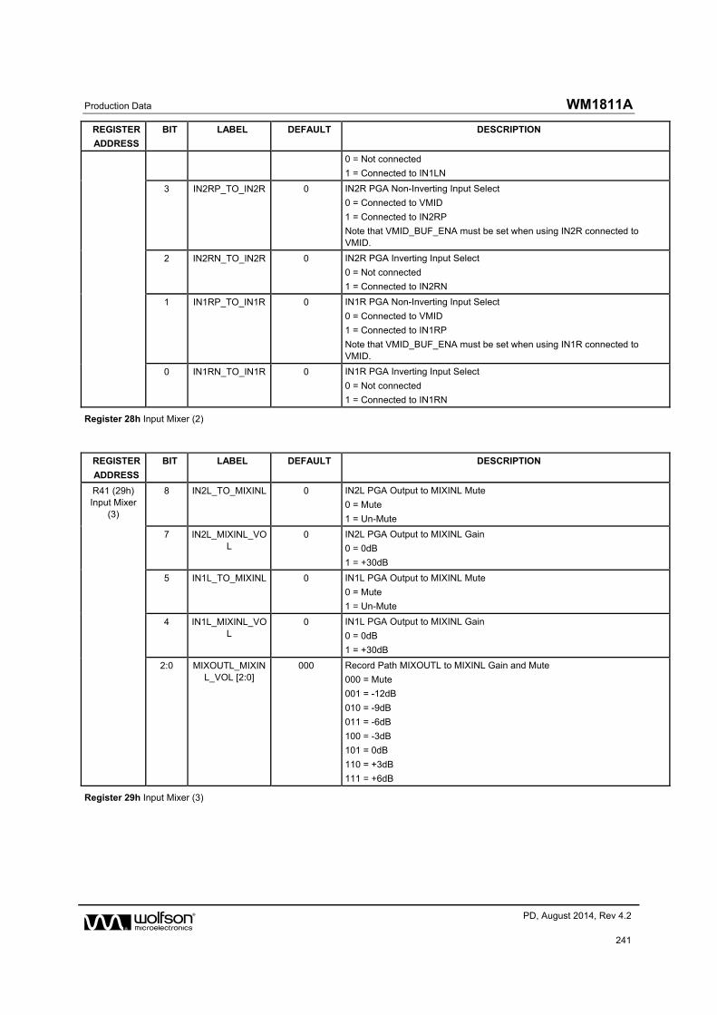
Production Data WM1811A
w PD, August 2014, Rev 4.2
241
REGISTER
ADDRESS
BIT LABEL DEFAULT DESCRIPTION
0 = Not connected
1 = Connected to IN1LN
3 IN2RP_TO_IN2R 0 IN2R PGA Non-Inverting Input Select
0 = Connected to VMID
1 = Connected to IN2RP
Note that VMID_BUF_ENA must be set when using IN2R connected to VMID.
2 IN2RN_TO_IN2R 0 IN2R PGA Inverting Input Select
0 = Not connected
1 = Connected to IN2RN
1 IN1RP_TO_IN1R 0 IN1R PGA Non-Inverting Input Select
0 = Connected to VMID
1 = Connected to IN1RP
Note that VMID_BUF_ENA must be set when using IN1R connected to VMID.
0 IN1RN_TO_IN1R 0 IN1R PGA Inverting Input Select
0 = Not connected
1 = Connected to IN1RN
Register 28h Input Mixer (2)
REGISTER
ADDRESS
BIT LABEL DEFAULT DESCRIPTION
R41 (29h) Input Mixer
(3)
8 IN2L_TO_MIXINL 0 IN2L PGA Output to MIXINL Mute
0 = Mute
1 = Un-Mute
7 IN2L_MIXINL_VOL
0 IN2L PGA Output to MIXINL Gain
0 = 0dB
1 = +30dB
5 IN1L_TO_MIXINL 0 IN1L PGA Output to MIXINL Mute
0 = Mute
1 = Un-Mute
4 IN1L_MIXINL_VOL
0 IN1L PGA Output to MIXINL Gain
0 = 0dB
1 = +30dB
2:0 MIXOUTL_MIXINL_VOL [2:0]
000 Record Path MIXOUTL to MIXINL Gain and Mute
000 = Mute
001 = -12dB
010 = -9dB
011 = -6dB
100 = -3dB
101 = 0dB
110 = +3dB
111 = +6dB
Register 29h Input Mixer (3)

WM1811A Production Data
w PD, August 2014, Rev 4.2
242
REGISTER
ADDRESS
BIT LABEL DEFAULT DESCRIPTION
R42 (2Ah) Input Mixer
(4)
8 IN2R_TO_MIXINR
0 IN2R PGA Output to MIXINR Mute
0 = Mute
1 = Un-Mute
7 IN2R_MIXINR_VOL
0 IN2R PGA Output to MIXINR Gain
0 = 0dB
1 = +30dB
5 IN1R_TO_MIXINR
0 IN1R PGA Output to MIXINR Mute
0 = Mute
1 = Un-Mute
4 IN1R_MIXINR_VOL
0 IN1R PGA Output to MIXINR Gain
0 = 0dB
1 = +30dB
2:0 MIXOUTR_MIXINR_VOL [2:0]
000 Record Path MIXOUTR to MIXINR Gain and Mute
000 = Mute
001 = -12dB
010 = -9dB
011 = -6dB
100 = -3dB
101 = 0dB
110 = +3dB
111 = +6dB
Register 2Ah Input Mixer (4)
REGISTER
ADDRESS
BIT LABEL DEFAULT DESCRIPTION
R43 (2Bh) Input Mixer
(5)
8:6 IN1LP_MIXINL_VOL [2:0]
000 IN1LP Pin (PGA Bypass) to MIXINL Gain and Mute
000 = Mute
001 = -12dB
010 = -9dB
011 = -6dB
100 = -3dB
101 = 0dB
110 = +3dB
111 = +6dB (see note below).
When IN1LP_MIXINL_BOOST is set, then the maximum gain setting is increased to +15dB, ie. 111 = +15dB.
Note that VMID_BUF_ENA must be set when using the IN1LP (PGA Bypass) input to MIXINL.
2:0 IN2LRP_MIXINL_VOL [2:0]
000 RXVOICE Differential Input (VRXP-VRXN) to MIXINL Gain and Mute
000 = Mute
001 = -12dB
010 = -9dB
011 = -6dB
100 = -3dB
101 = 0dB
110 = +3dB
111 = +6dB
Register 2Bh Input Mixer (5)

Production Data WM1811A
w PD, August 2014, Rev 4.2
243
REGISTER
ADDRESS
BIT LABEL DEFAULT DESCRIPTION
R44 (2Ch) Input Mixer
(6)
8:6 IN1RP_MIXINR_VOL [2:0]
000 IN1RP Pin (PGA Bypass) to MIXINR Gain and Mute
000 = Mute
001 = -12dB
010 = -9dB
011 = -6dB
100 = -3dB
101 = 0dB
110 = +3dB
111 = +6dB (see note below).
When IN1RP_MIXINR_BOOST is set, then the maximum gain setting is increased to +15dB, ie. 111 = +15dB.
Note that VMID_BUF_ENA must be set when using the IN1RP (PGA Bypass) input to MIXINR.
2:0 IN2LRP_MIXINR_VOL [2:0]
000 RXVOICE Differential Input (VRXP-VRXN) to MIXINR Gain and Mute
000 = Mute
001 = -12dB
010 = -9dB
011 = -6dB
100 = -3dB
101 = 0dB
110 = +3dB
111 = +6dB
Register 2Ch Input Mixer (6)
REGISTER
ADDRESS
BIT LABEL DEFAULT DESCRIPTION
R45 (2Dh) Output Mixer
(1)
8 DAC1L_TO_HPOUT1L
0 HPOUT1LVOL (Left Headphone Output PGA) Input Select
0 = MIXOUTL
1 = DACL
7 MIXINR_TO_MIXOUTL
0 MIXINR Output (Right ADC bypass) to MIXOUTL Mute
0 = Mute
1 = Un-mute
6 MIXINL_TO_MIXOUTL
0 MIXINL Output (Left ADC bypass) to MIXOUTL Mute
0 = Mute
1 = Un-mute
5 IN2RN_TO_MIXOUTL
0 IN2RN to MIXOUTL Mute
0 = Mute
1 = Un-mute
Note that VMID_BUF_ENA must be set when using the IN2RN input to MIXOUTL.
4 IN2LN_TO_MIXOUTL
0 IN2LN to MIXOUTL Mute
0 = Mute
1 = Un-mute
Note that VMID_BUF_ENA must be set when using the IN2LN input to MIXOUTL.
3 IN1R_TO_MIXOUTL
0 IN1R PGA Output to MIXOUTL Mute
0 = Mute
1 = Un-mute
2 IN1L_TO_MIXOUTL
0 IN1L PGA Output to MIXOUTL Mute
0 = Mute
1 = Un-mute

WM1811A Production Data
w PD, August 2014, Rev 4.2
244
REGISTER
ADDRESS
BIT LABEL DEFAULT DESCRIPTION
1 IN2LP_TO_MIXOUTL
0 IN2LP to MIXOUTL Mute
0 = Mute
1 = Un-mute
Note that VMID_BUF_ENA must be set when using the IN2LP input to MIXOUTL.
0 DAC1L_TO_MIXOUTL
0 Left DAC to MIXOUTL Mute
0 = Mute
1 = Un-mute
Register 2Dh Output Mixer (1)
REGISTER
ADDRESS
BIT LABEL DEFAULT DESCRIPTION
R46 (2Eh) Output Mixer
(2)
8 DAC1R_TO_HPOUT1R
0 HPOUT1RVOL (Right Headphone Output PGA) Input Select
0 = MIXOUTR
1 = DACR
7 MIXINL_TO_MIXOUTR
0 MIXINL Output (Left ADC bypass) to MIXOUTR Mute
0 = Mute
1 = Un-mute
6 MIXINR_TO_MIXOUTR
0 MIXINR Output (Right ADC bypass) to MIXOUTR Mute
0 = Mute
1 = Un-mute
5 IN2LN_TO_MIXOUTR
0 IN2LN to MIXOUTR Mute
0 = Mute
1 = Un-mute
Note that VMID_BUF_ENA must be set when using the IN2LN input to MIXOUTR.
4 IN2RN_TO_MIXOUTR
0 IN2RN to MIXOUTR Mute
0 = Mute
1 = Un-mute
Note that VMID_BUF_ENA must be set when using the IN2RN input to MIXOUTR.
3 IN1L_TO_MIXOUTR
0 IN1L PGA Output to MIXOUTR Mute
0 = Mute
1 = Un-mute
2 IN1R_TO_MIXOUTR
0 IN1R PGA Output to MIXOUTR Mute
0 = Mute
1 = Un-mute
1 IN2RP_TO_MIXOUTR
0 IN2RP to MIXOUTR Mute
0 = Mute
1 = Un-mute
Note that VMID_BUF_ENA must be set when using the IN2RP input to MIXOUTR.
0 DAC1R_TO_MIXOUTR
0 Right DAC to MIXOUTR Mute
0 = Mute
1 = Un-mute
Register 2Eh Output Mixer (2)

Production Data WM1811A
w PD, August 2014, Rev 4.2
245
REGISTER
ADDRESS
BIT LABEL DEFAULT DESCRIPTION
R47 (2Fh) Output Mixer
(3)
11:9 IN2LP_MIXOUTL_VOL [2:0]
000 IN2LP to MIXOUTL Volume
0dB to -9dB in 3dB steps
X00 = 0dB
X01 = -3dB
X10 = -6dB
X11 = -9dB
8:6 IN2LN_MIXOUTL_VOL [2:0]
000 IN2LN to MIXOUTL Volume
0dB to -9dB in 3dB steps
X00 = 0dB
X01 = -3dB
X10 = -6dB
X11 = -9dB
5:3 IN1R_MIXOUTL_VOL [2:0]
000 IN1R PGA Output to MIXOUTL Volume
0dB to -9dB in 3dB steps
X00 = 0dB
X01 = -3dB
X10 = -6dB
X11 = -9dB
2:0 IN1L_MIXOUTL_VOL [2:0]
000 IN1L PGA Output to MIXOUTL Volume
0dB to -9dB in 3dB steps
X00 = 0dB
X01 = -3dB
X10 = -6dB
X11 = -9dB
Register 2Fh Output Mixer (3)
REGISTER
ADDRESS
BIT LABEL DEFAULT DESCRIPTION
R48 (30h) Output Mixer
(4)
11:9 IN2RP_MIXOUTR_VOL [2:0]
000 IN2RP to MIXOUTR Volume
0dB to -9dB in 3dB steps
X00 = 0dB
X01 = -3dB
X10 = -6dB
X11 = -9dB
8:6 IN2RN_MIXOUTR_VOL [2:0]
000 IN2RN to MIXOUTR Volume
0dB to -9dB in 3dB steps
X00 = 0dB
X01 = -3dB
X10 = -6dB
X11 = -9dB
5:3 IN1L_MIXOUTR_VOL [2:0]
000 IN1L PGA Output to MIXOUTR Volume
0dB to -9dB in 3dB steps
X00 = 0dB
X01 = -3dB
X10 = -6dB
X11 = -9dB

WM1811A Production Data
w PD, August 2014, Rev 4.2
246
REGISTER
ADDRESS
BIT LABEL DEFAULT DESCRIPTION
2:0 IN1R_MIXOUTR_VOL [2:0]
000 IN1R PGA Output to MIXOUTR Volume
0dB to -9dB in 3dB steps X00 = 0dB X01 = -3dB X10 = -6dB X11 = -9dB
Register 30h Output Mixer (4)
REGISTER
ADDRESS
BIT LABEL DEFAULT DESCRIPTION
R49 (31h) Output Mixer
(5)
11:9 DAC1L_MIXOUTL_VOL [2:0]
000 Left DAC to MIXOUTL Volume
0dB to -9dB in 3dB steps
X00 = 0dB
X01 = -3dB
X10 = -6dB
X11 = -9dB
8:6 IN2RN_MIXOUTL_VOL [2:0]
000 IN2RN to MIXOUTL Volume
0dB to -9dB in 3dB steps
X00 = 0dB
X01 = -3dB
X10 = -6dB
X11 = -9dB
5:3 MIXINR_MIXOUTL_VOL [2:0]
000 MIXINR Output (Right ADC bypass) to MIXOUTL Volume
0dB to -9dB in 3dB steps
X00 = 0dB
X01 = -3dB
X10 = -6dB
X11 = -9dB
2:0 MIXINL_MIXOUTL_VOL [2:0]
000 MIXINL Output (Left ADC bypass) to MIXOUTL Volume
0dB to -9dB in 3dB steps
X00 = 0dB
X01 = -3dB
X10 = -6dB
X11 = -9dB
Register 31h Output Mixer (5)
REGISTER
ADDRESS
BIT LABEL DEFAULT DESCRIPTION
R50 (32h) Output Mixer
(6)
11:9 DAC1R_MIXOUTR_VOL [2:0]
000 Right DAC to MIXOUTR Volume
0dB to -9dB in 3dB steps
X00 = 0dB
X01 = -3dB
X10 = -6dB
X11 = -9dB
8:6 IN2LN_MIXOUTR_VOL [2:0]
000 IN2LN to MIXOUTR Volume
0dB to -9dB in 3dB steps
X00 = 0dB
X01 = -3dB
X10 = -6dB
X11 = -9dB

Production Data WM1811A
w PD, August 2014, Rev 4.2
247
REGISTER
ADDRESS
BIT LABEL DEFAULT DESCRIPTION
5:3 MIXINL_MIXOUTR_VOL [2:0]
000 MIXINL Output (Left ADC bypass) to MIXOUTR Volume
0dB to -9dB in 3dB steps
X00 = 0dB
X01 = -3dB
X10 = -6dB
X11 = -9dB
2:0 MIXINR_MIXOUTR_VOL [2:0]
000 MIXINR Output (Right ADC bypass) to MIXOUTR Volume
0dB to -9dB in 3dB steps
X00 = 0dB
X01 = -3dB
X10 = -6dB
X11 = -9dB
Register 32h Output Mixer (6)
REGISTER
ADDRESS
BIT LABEL DEFAULT DESCRIPTION
R51 (33h) HPOUT2
Mixer
4 MIXOUTLVOL_TO_HPOUT2
0 MIXOUTLVOL (Left Output Mixer PGA) to Earpiece Driver
0 = Mute
1 = Un-mute
3 MIXOUTRVOL_TO_HPOUT2
0 MIXOUTRVOL (Right Output Mixer PGA) to Earpiece Driver
0 = Mute
1 = Un-mute
Register 33h HPOUT2 Mixer
REGISTER
ADDRESS
BIT LABEL DEFAULT DESCRIPTION
R52 (34h) Line Mixer (1)
6 MIXOUTL_TO_LINEOUT1N
0 MIXOUTL to Single-Ended Line Output on LINEOUT1N
0 = Mute
1 = Un-mute
(LINEOUT1_MODE = 1)
5 MIXOUTR_TO_LINEOUT1N
0 MIXOUTR to Single-Ended Line Output on LINEOUT1N
0 = Mute
1 = Un-mute
(LINEOUT1_MODE = 1)
4 LINEOUT1_MODE
0 LINEOUT1 Mode Select
0 = Differential
1 = Single-Ended
2 IN1R_TO_LINEOUT1P
0 IN1R Input PGA to Differential Line Output on LINEOUT1
0 = Mute
1 = Un-mute
(LINEOUT1_MODE = 0)
1 IN1L_TO_LINEOUT1P
0 IN1L Input PGA to Differential Line Output on LINEOUT1
0 = Mute
1 = Un-mute
(LINEOUT1_MODE = 0)
0 MIXOUTL_TO_LINEOUT1P
0 Differential Mode (LINEOUT1_MODE = 0):
MIXOUTL to Differential Output on LINEOUT1
0 = Mute
1 = Un-mute

WM1811A Production Data
w PD, August 2014, Rev 4.2
248
REGISTER
ADDRESS
BIT LABEL DEFAULT DESCRIPTION
Single Ended Mode (LINEOUT1_MODE = 1):
MIXOUTL to Single-Ended Line Output on LINEOUT1P
0 = Mute
1 = Un-mute
Register 34h Line Mixer (1)
REGISTER
ADDRESS
BIT LABEL DEFAULT DESCRIPTION
R53 (35h) Line Mixer (2)
6 MIXOUTR_TO_LINEOUT2N
0 MIXOUTR to Single-Ended Line Output on LINEOUT2N
0 = Mute
1 = Un-mute
(LINEOUT2_MODE = 1)
5 MIXOUTL_TO_LINEOUT2N
0 MIXOUTL to Single-Ended Line Output on LINEOUT2N
0 = Mute
1 = Un-mute
(LINEOUT2_MODE = 1)
4 LINEOUT2_MODE
0 LINEOUT2 Mode Select
0 = Differential
1 = Single-Ended
2 IN1L_TO_LINEOUT2P
0 IN1L Input PGA to Differential Line Output on LINEOUT2
0 = Mute
1 = Un-mute
(LINEOUT2_MODE = 0)
1 IN1R_TO_LINEOUT2P
0 IN1R Input PGA to Differential Line Output on LINEOUT2
0 = Mute
1 = Un-mute
(LINEOUT2_MODE = 0)
0 MIXOUTR_TO_LINEOUT2P
0 Differential Mode (LINEOUT2_MODE = 0):
MIXOUTR to Differential Output on LINEOUT2
0 = Mute
1 = Un-mute
Single-Ended Mode (LINEOUT2_MODE = 0):
MIXOUTR to Single-Ended Line Output on LINEOUT2P
0 = Mute
1 = Un-mute
Register 35h Line Mixer (2)
REGISTER
ADDRESS
BIT LABEL DEFAULT DESCRIPTION
R54 (36h) Speaker
Mixer
7 MIXINL_TO_SPKMIXL
0 MIXINL (Left ADC bypass) to SPKMIXL Mute
0 = Mute
1 = Un-mute
6 MIXINR_TO_SPKMIXR
0 MIXINR (Right ADC bypass) to SPKMIXR Mute
0 = Mute
1 = Un-mute
5 IN1LP_TO_SPKMIXL
0 IN1LP to SPKMIXL Mute
0 = Mute

Production Data WM1811A
w PD, August 2014, Rev 4.2
249
REGISTER
ADDRESS
BIT LABEL DEFAULT DESCRIPTION
1 = Un-mute
Note that VMID_BUF_ENA must be set when using the IN1LP input to SPKMIXL.
4 IN1RP_TO_SPKMIXR
0 IN1RP to SPKMIXR Mute
0 = Mute
1 = Un-mute
Note that VMID_BUF_ENA must be set when using the IN1RP input to SPKMIXR.
3 MIXOUTL_TO_SPKMIXL
0 Left Mixer Output to SPKMIXL Mute
0 = Mute
1 = Un-mute
2 MIXOUTR_TO_SPKMIXR
0 Right Mixer Output to SPKMIXR Mute
0 = Mute
1 = Un-mute
1 DAC1L_TO_SPKMIXL
0 Left DAC to SPKMIXL Mute
0 = Mute
1 = Un-mute
0 DAC1R_TO_SPKMIXR
0 Right DAC to SPKMIXR Mute
0 = Mute
1 = Un-mute
Register 36h Speaker Mixer
REGISTER
ADDRESS
BIT LABEL DEFAULT DESCRIPTION
R55 (37h) Additional
Control
7 LINEOUT1_FB 0 Enable ground loop noise feedback on LINEOUT1
0 = Disabled
1 = Enabled
6 LINEOUT2_FB 0 Enable ground loop noise feedback on LINEOUT2
0 = Disabled
1 = Enabled
0 VROI 0 Buffered VMID to Analogue Line Output Resistance (Disabled Outputs)
0 = 20kohm from buffered VMID to output
1 = 500ohm from buffered VMID to output
Register 37h Additional Control
REGISTER
ADDRESS
BIT LABEL DEFAULT DESCRIPTION
R56 (38h) AntiPOP (1)
7 LINEOUT_VMID_BUF_ENA
0 Enables VMID reference for line outputs in single-ended mode
0 = Disabled
1 = Enabled
6 HPOUT2_IN_ENA
0 HPOUT2MIX Mixer and Input Stage Enable
0 = Disabled
1 = Enabled
5 LINEOUT1_DISCH
0 Discharges LINEOUT1P and LINEOUT1N outputs
0 = Not active
1 = Actively discharging LINEOUT1P and LINEOUT1N
4 LINEOUT2_DISCH
0 Discharges LINEOUT2P and LINEOUT2N outputs
0 = Not active
1 = Actively discharging LINEOUT2P and LINEOUT2N
Register 38h AntiPOP (1)

WM1811A Production Data
w PD, August 2014, Rev 4.2
250
REGISTER
ADDRESS
BIT LABEL DEFAULT DESCRIPTION
R57 (39h) AntiPOP (2)
8:7 JACKDET_MODE [1:0]
00 JACKDET mode select
00 = Jack Detect disabled
01 = Jack Detect enabled
10 = Jack Detect enabled
11 = Jack Detect enabled
MICDET (microphone/accessory detection) is not supported when JACKDET_MODE = 10.
Analogue/Digital audio functions are not supported when JACKDET_MODE = 01 or 10.
LDO1_DISCH must be set to 0 when JACKDET_MODE = 01.
Settings 01 and 10 must not be selected if AVDD1 or DCVDD is supplied externally (ie. if LDO1 or LDO2 is not used).
6:5 VMID_RAMP [1:0] 00 VMID soft start enable / slew rate control
00 = Normal slow start
01 = Normal fast start
10 = Soft slow start
11 = Soft fast start
If VMID_RAMP = 1X is selected for VMID start-up or shut-down, then the soft-start circuit must be reset by setting VMID_RAMP=00 after VMID is disabled, before VMID is re-enabled. VMID is disabled / enabled using the VMID_SEL register.
3 VMID_BUF_ENA 0 VMID Buffer Enable
0 = Disabled
1 = Enabled (provided VMID_SEL > 00)
2 STARTUP_BIAS_ENA
0 Enables the Start-Up bias current generator
0 = Disabled
1 = Enabled
1 BIAS_SRC 0 Selects the bias current source
0 = Normal bias
1 = Start-Up bias
0 VMID_DISCH 0 Connects VMID to ground
0 = Disabled
1 = Enabled
Register 39h AntiPOP (2)
REGISTER
ADDRESS
BIT LABEL DEFAULT DESCRIPTION
R59 (3Bh) LDO 1
3:1 LDO1_VSEL [2:0] 110 LDO1 Output Voltage Select
2.4V to 3.1V in 100mV steps
000 = 2.4V
001 = 2.5V
010 = 2.6V
011 = 2.7V
100 = 2.8V
101 = 2.9V
110 = 3.0V
111 = 3.1V

Production Data WM1811A
w PD, August 2014, Rev 4.2
251
REGISTER
ADDRESS
BIT LABEL DEFAULT DESCRIPTION
0 LDO1_DISCH 1 LDO1 Discharge Select
0 = LDO1 floating when disabled
1 = LDO1 discharged when disabled
Register 3Bh LDO 1
REGISTER
ADDRESS
BIT LABEL DEFAULT DESCRIPTION
R60 (3Ch) LDO 2
2:1 LDO2_VSEL [1:0] 01 LDO2 Output Voltage Select
1.05V to 1.25V in 100mV steps
00 = Reserved
01 = 1.05V
10 = 1.15V
11 = 1.25V
0 LDO2_DISCH 1 LDO2 Discharge Select
0 = LDO2 floating when disabled
1 = LDO2 discharged when disabled
Register 3Ch LDO 2
REGISTER
ADDRESS
BIT LABEL DEFAULT DESCRIPTION
R61 (3Dh) MICBIAS1
5 MICB1_RATE 1 Microphone Bias 1 Rate
0 = Fast start-up / shut-down
1 = Pop-free start-up / shut-down
4 MICB1_MODE 1 Microphone Bias 1 Mode
0 = Regulator mode
1 = Bypass mode
3:1 MICB1_LVL [2:0] 100 Microphone Bias 1 Voltage Control
(when MICB1_MODE = 0) 000 = 1.5V 001 = 1.8V 010 = 1.9V 011 = 2.0V 100 = 2.2V 101 = 2.4V 110 = 2.5V 111 = 2.6V
0 MICB1_DISCH 1 Microphone Bias 1 Discharge
0 = MICBIAS1 floating when disabled
1 = MICBIAS1 discharged when disabled
Register 3Dh MICBIAS1
REGISTER
ADDRESS
BIT LABEL DEFAULT DESCRIPTION
R62 (3Eh) MICBIAS2
5 MICB2_RATE 1 Microphone Bias 2 Rate
0 = Fast start-up / shut-down
1 = Pop-free start-up / shut-down
4 MICB2_MODE 1 Microphone Bias 2 Mode
0 = Regulator mode
1 = Bypass mode

WM1811A Production Data
w PD, August 2014, Rev 4.2
252
REGISTER
ADDRESS
BIT LABEL DEFAULT DESCRIPTION
3:1 MICB2_LVL [2:0] 100 Microphone Bias 2 Voltage Control
(when MICB2_MODE = 0)
000 = 1.5V
001 = 1.8V
010 = 1.9V
011 = 2.0V
100 = 2.2V
101 = 2.4V
110 = 2.5V
111 = 2.6V
0 MICB2_DISCH 1 Microphone Bias 2 Discharge
0 = MICBIAS2 floating when disabled
1 = MICBIAS2 discharged when disabled
Register 3Eh MICBIAS2
REGISTER
ADDRESS
BIT LABEL DEFAULT DESCRIPTION
R76 (4Ch) Charge Pump
(1)
15 CP_ENA 0 Enable charge-pump digits
0 = Disable
1 = Enable
Register 4Ch Charge Pump (1)
REGISTER
ADDRESS
BIT LABEL DEFAULT DESCRIPTION
R77 (4Dh) Charge Pump
(2)
15 CP_DISCH 1 Charge Pump Discharge Select
0 = Charge Pump outputs floating when disabled
1 = Charge Pump outputs discharged when disabled
Register 4Dh Charge Pump (2)
REGISTER
ADDRESS
BIT LABEL DEFAULT DESCRIPTION
R81 (51h) Class W (1)
9:8 CP_DYN_SRC_SEL [1:0]
00 Selects the digital audio source for envelope tracking
00 = AIF1, DAC data
01 = Reserved
10 = AIF2, DAC data
11 = Reserved
0 CP_DYN_PWR 0 Enable dynamic charge pump power control
0 = charge pump controlled by volume register settings (Class G)
1 = charge pump controlled by real-time audio level (Class W)
Register 51h Class W (1)
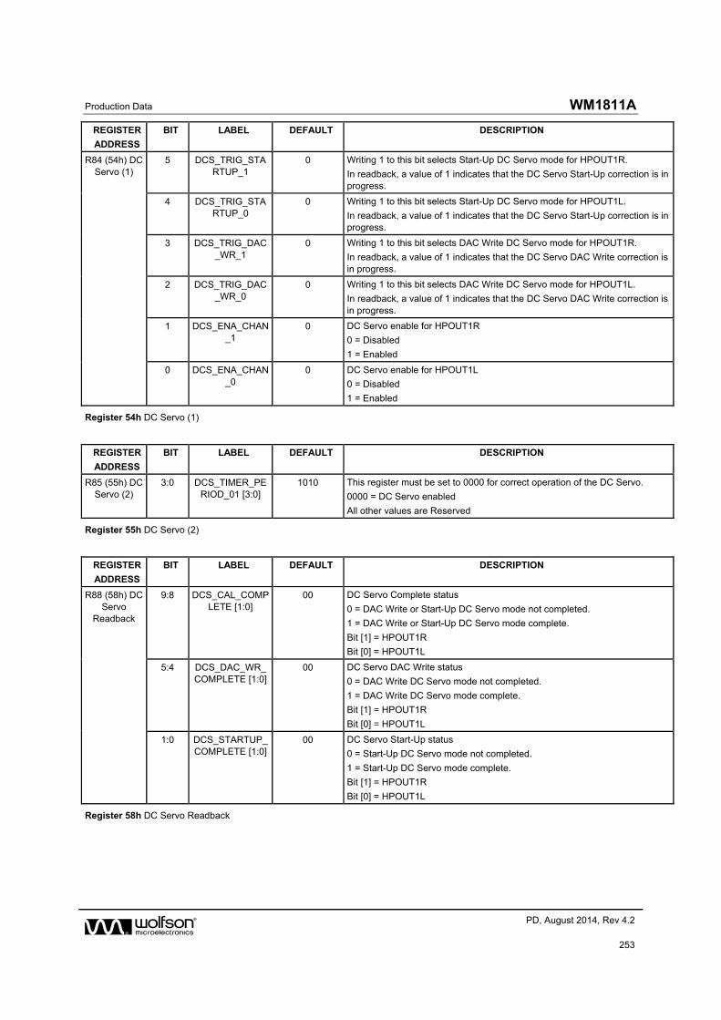
Production Data WM1811A
w PD, August 2014, Rev 4.2
253
REGISTER
ADDRESS
BIT LABEL DEFAULT DESCRIPTION
R84 (54h) DC Servo (1)
5 DCS_TRIG_STARTUP_1
0 Writing 1 to this bit selects Start-Up DC Servo mode for HPOUT1R.
In readback, a value of 1 indicates that the DC Servo Start-Up correction is in progress.
4 DCS_TRIG_STARTUP_0
0 Writing 1 to this bit selects Start-Up DC Servo mode for HPOUT1L.
In readback, a value of 1 indicates that the DC Servo Start-Up correction is in progress.
3 DCS_TRIG_DAC_WR_1
0 Writing 1 to this bit selects DAC Write DC Servo mode for HPOUT1R.
In readback, a value of 1 indicates that the DC Servo DAC Write correction is in progress.
2 DCS_TRIG_DAC_WR_0
0 Writing 1 to this bit selects DAC Write DC Servo mode for HPOUT1L.
In readback, a value of 1 indicates that the DC Servo DAC Write correction is in progress.
1 DCS_ENA_CHAN_1
0 DC Servo enable for HPOUT1R
0 = Disabled
1 = Enabled
0 DCS_ENA_CHAN_0
0 DC Servo enable for HPOUT1L
0 = Disabled
1 = Enabled
Register 54h DC Servo (1)
REGISTER
ADDRESS
BIT LABEL DEFAULT DESCRIPTION
R85 (55h) DC Servo (2)
3:0 DCS_TIMER_PERIOD_01 [3:0]
1010 This register must be set to 0000 for correct operation of the DC Servo.
0000 = DC Servo enabled
All other values are Reserved
Register 55h DC Servo (2)
REGISTER
ADDRESS
BIT LABEL DEFAULT DESCRIPTION
R88 (58h) DC Servo
Readback
9:8 DCS_CAL_COMPLETE [1:0]
00 DC Servo Complete status
0 = DAC Write or Start-Up DC Servo mode not completed.
1 = DAC Write or Start-Up DC Servo mode complete.
Bit [1] = HPOUT1R
Bit [0] = HPOUT1L
5:4 DCS_DAC_WR_COMPLETE [1:0]
00 DC Servo DAC Write status
0 = DAC Write DC Servo mode not completed.
1 = DAC Write DC Servo mode complete.
Bit [1] = HPOUT1R
Bit [0] = HPOUT1L
1:0 DCS_STARTUP_COMPLETE [1:0]
00 DC Servo Start-Up status
0 = Start-Up DC Servo mode not completed.
1 = Start-Up DC Servo mode complete.
Bit [1] = HPOUT1R
Bit [0] = HPOUT1L
Register 58h DC Servo Readback

WM1811A Production Data
w PD, August 2014, Rev 4.2
254
REGISTER
ADDRESS
BIT LABEL DEFAULT DESCRIPTION
R89 (59h) DC Servo (4)
15:8 DCS_DAC_WR_VAL_1 [7:0]
0000_0000 Writing to this field sets the DC Offset value for HPOUT1R in DAC Write DC Servo mode.
Reading this field gives the current DC Offset value for HPOUT1R.
Two’s complement format.
LSB is 0.25mV.
Range is -32mV to +31.75mV
7:0 DCS_DAC_WR_VAL_0 [7:0]
0000_0000 Writing to this field sets the DC Offset value for HPOUT1L in DAC Write DC Servo mode.
Reading this field gives the current DC Offset value for HPOUT1L.
Two’s complement format.
LSB is 0.25mV.
Range is -32mV to +31.75mV
Register 59h DC Servo (4)

Production Data WM1811A
w PD, August 2014, Rev 4.2
255
REGISTER
ADDRESS
BIT LABEL DEFAULT DESCRIPTION
R96 (60h) Analogue HP
(1)
8 HPOUT1_ATTN 0 HPOUT1L and HPOUT1R Attenuation
0 = 0dB
1 = -3dB
Note that, when CP_DYN_PWR=0, then any update to HPOUT1_ATTN is not fully implemented until a ‘1’ is written to HPOUT1_VU.
7 HPOUT1L_RMV_SHORT
0 Removes HPOUT1L short
0 = HPOUT1L short enabled
1 = HPOUT1L short removed
For normal operation, this bit should be set as the final step of the HPOUT1L Enable sequence.
6 HPOUT1L_OUTP 0 Enables HPOUT1L output stage
0 = Disabled
1 = Enabled
For normal operation, this bit should be set to 1 after the DC offset cancellation has been scheduled.
5 HPOUT1L_DLY 0 Enables HPOUT1L intermediate stage
0 = Disabled
1 = Enabled
For normal operation, this bit should be set to 1 after the output signal path has been configured, and before DC offset cancellation is scheduled. This bit should be set with at least 20us delay after HPOUT1L_ENA.
3 HPOUT1R_RMV_SHORT
0 Removes HPOUT1R short
0 = HPOUT1R short enabled
1 = HPOUT1R short removed
For normal operation, this bit should be set as the final step of the HPOUT1R Enable sequence.
2 HPOUT1R_OUTP 0 Enables HPOUT1R output stage
0 = Disabled
1 = Enabled
For normal operation, this bit should be set to 1 after the DC offset cancellation has been scheduled.
1 HPOUT1R_DLY 0 Enables HPOUT1R intermediate stage
0 = Disabled
1 = Enabled
For normal operation, this bit should be set to 1 after the output signal path has been configured, and before DC offset cancellation is scheduled. This bit should be set with at least 20us delay after HPOUT1R_ENA.
Register 60h Analogue HP (1)
REGISTER
ADDRESS
BIT LABEL DEFAULT DESCRIPTION
R197 (C5h) Class D Test
(5)
0 SPKOUT_CLK_SRC
0 Selects the source for the CLASSD speaker clock
0: selects undithered clock
1: selects dithered clock
Register C5h Class D Test (5)

WM1811A Production Data
w PD, August 2014, Rev 4.2
256
REGISTER
ADDRESS
BIT LABEL DEFAULT DESCRIPTION
R208 (D0h) Mic Detect 1
15:12 MICD_BIAS_STARTTIME [3:0]
0111 Mic Detect Bias Startup Delay
(If MICBIAS2 is not enabled already, this field selects the delay time allowed for MICBIAS2 to startup prior to performing the MICDET function.) 0000 = 0ms (continuous) 0001 = 0.25ms 0010 = 0.5ms 0011 = 1ms 0100 = 2ms 0101 = 4ms 0110 = 8ms 0111 = 16ms 1000 = 32ms 1001 = 64ms 1010 = 128ms 1011 = 256ms 1100 to 1111 = 512ms
11:8 MICD_RATE [3:0] 0110 Mic Detect Rate
(Selects the delay between successive Mic Detect measurements.) 0000 = 0ms (continuous) 0001 = 0.25ms 0010 = 0.5ms 0011 = 1ms 0100 = 2ms 0101 = 4ms 0110 = 8ms 0111 = 16ms 1000 = 32ms 1001 = 64ms 1010 = 128ms 1011 = 256ms 1100 to 1111 = 512ms
1 MICD_DBTIME 0 Mic Detect De-bounce
0 = 2 measurements
1 = 4 measurements
0 MICD_ENA 0 Mic Detect Enable
0 = Disabled
1 = Enabled
Note that Mic Detect is not supported when JACKDET_MODE = 10.
Register D0h Mic Detect 1

Production Data WM1811A
w PD, August 2014, Rev 4.2
257
REGISTER
ADDRESS
BIT LABEL DEFAULT DESCRIPTION
R209 (D1h) Mic Detect 2
7:0 MICD_LVL_SEL [7:0]
0111_1111 Mic Detect Level Select
(enables Mic Detection in specific impedance ranges)
[7] = Not used - must be set to 0
[6] = Enable >475 ohm detection
[5] = Enable 326 ohm detection
[4] = Enable 152 ohm detection
[3] = Enable 77 ohm detection
[2] = Enable 47.6 ohm detection
[1] = Enable 29.4 ohm detection
[0] = Enable 14 ohm detection
Note that the impedance values quoted assume that a microphone (475ohm-30kohm) is also present on the MICDET pin.
Register D1h Mic Detect 2
REGISTER
ADDRESS
BIT LABEL DEFAULT DESCRIPTION
R210 (D2h) Mic Detect 3
10:2 MICD_LVL [8:0] 0_0000_0000 Mic Detect Level
(indicates the measured impedance)
[8] = Not used
[7] = >475 ohm, <30k ohm
[6] = 326 ohm
[5] = 152 ohm
[4] = 77 ohm
[3] = 47.6 ohm
[2] = 29.4 ohm
[1] = 14 ohm
[0] = <3 ohm
Note that the impedance values quoted assume that a microphone (475ohm-30kohm) is also present on the MICDET pin.
1 MICD_VALID 0 Mic Detect Data Valid
0 = Not Valid
1 = Valid
0 MICD_STS 0 Mic Detect Status
0 = No Mic Accessory present(impedance is >30k ohm)
1 = Mic Accessory is present(impedance is <30k ohm)
Register D2h Mic Detect 3
REGISTER
ADDRESS
BIT LABEL DEFAULT DESCRIPTION
R256 (0100h) Chip Revision
15:8 CUST_ID [7:0] Customer ID
3:0 CHIP_REV [3:0] Chip revision
Register 0100h Chip Revision

WM1811A Production Data
w PD, August 2014, Rev 4.2
258
REGISTER
ADDRESS
BIT LABEL DEFAULT DESCRIPTION
R257 (0101h) Control
Interface
15 Reserved 1 Reserved - do not change
2 AUTO_INC 1 Enables address auto-increment
0 = Disabled
1 = Enabled
Register 0101h Control Interface
REGISTER
ADDRESS
BIT LABEL DEFAULT DESCRIPTION
R512 (0200h) AIF1
Clocking (1)
4:3 AIF1CLK_SRC [1:0]
00 AIF1CLK Source Select
00 = MCLK1
01 = MCLK2
10 = FLL1
11 = FLL2
2 AIF1CLK_INV 0 AIF1CLK Invert
0 = AIF1CLK not inverted
1 = AIF1CLK inverted
1 AIF1CLK_DIV 0 AIF1CLK Divider
0 = AIF1CLK
1 = AIF1CLK / 2
0 AIF1CLK_ENA 0 AIF1CLK Enable
0 = Disabled
1 = Enabled
Register 0200h AIF1 Clocking (1)
REGISTER
ADDRESS
BIT LABEL DEFAULT DESCRIPTION
R513 (0201h) AIF1
Clocking (2)
5:3 AIF1DAC_DIV [2:0]
000 Selects the AIF1 input path sample rate relative to the AIF1 output path sample rate.
This field should only be changed from default in modes where the AIF1 input path sample rate is slower than the AIF1 output path sample rate.
000 = Divide by 1
001 = Divide by 1.5
010 = Divide by 2
011 = Divide by 3
100 = Divide by 4
101 = Divide by 5.5
110 = Divide by 6
111 = Reserved
2:0 AIF1ADC_DIV [2:0]
000 Selects the AIF1 output path sample rate relative to the AIF1 input path sample rate.
This field should only be changed from default in modes where the AIF1 output path sample rate is slower than the AIF1 input path sample rate.
000 = Divide by 1
001 = Divide by 1.5
010 = Divide by 2
011 = Divide by 3
100 = Divide by 4
101 = Divide by 5.5
110 = Divide by 6
111 = Reserved
Register 0201h AIF1 Clocking (2)
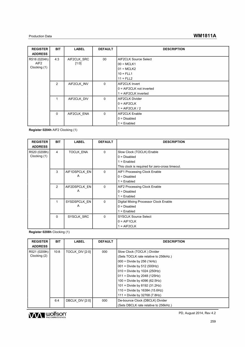
Production Data WM1811A
w PD, August 2014, Rev 4.2
259
REGISTER
ADDRESS
BIT LABEL DEFAULT DESCRIPTION
R516 (0204h) AIF2
Clocking (1)
4:3 AIF2CLK_SRC [1:0]
00 AIF2CLK Source Select
00 = MCLK1
01 = MCLK2
10 = FLL1
11 = FLL2
2 AIF2CLK_INV 0 AIF2CLK Invert
0 = AIF2CLK not inverted
1 = AIF2CLK inverted
1 AIF2CLK_DIV 0 AIF2CLK Divider
0 = AIF2CLK
1 = AIF2CLK / 2
0 AIF2CLK_ENA 0 AIF2CLK Enable
0 = Disabled
1 = Enabled
Register 0204h AIF2 Clocking (1)
REGISTER
ADDRESS
BIT LABEL DEFAULT DESCRIPTION
R520 (0208h) Clocking (1)
4 TOCLK_ENA 0 Slow Clock (TOCLK) Enable
0 = Disabled
1 = Enabled
This clock is required for zero-cross timeout.
3 AIF1DSPCLK_ENA
0 AIF1 Processing Clock Enable
0 = Disabled
1 = Enabled
2 AIF2DSPCLK_ENA
0 AIF2 Processing Clock Enable
0 = Disabled
1 = Enabled
1 SYSDSPCLK_ENA
0 Digital Mixing Processor Clock Enable
0 = Disabled
1 = Enabled
0 SYSCLK_SRC 0 SYSCLK Source Select
0 = AIF1CLK
1 = AIF2CLK
Register 0208h Clocking (1)
REGISTER
ADDRESS
BIT LABEL DEFAULT DESCRIPTION
R521 (0209h) Clocking (2)
10:8 TOCLK_DIV [2:0] 000 Slow Clock (TOCLK ) Divider
(Sets TOCLK rate relative to 256kHz.)
000 = Divide by 256 (1kHz)
001 = Divide by 512 (500Hz)
010 = Divide by 1024 (250Hz)
011 = Divide by 2048 (125Hz)
100 = Divide by 4096 (62.5Hz)
101 = Divide by 8192 (31.2Hz)
110 = Divide by 16384 (15.6Hz)
111 = Divide by 32768 (7.8Hz)
6:4 DBCLK_DIV [2:0] 000 De-bounce Clock (DBCLK) Divider
(Sets DBCLK rate relative to 256kHz.)

WM1811A Production Data
w PD, August 2014, Rev 4.2
260
REGISTER
ADDRESS
BIT LABEL DEFAULT DESCRIPTION
000 = Divide by 256 (1kHz)
001 = Divide by 2048 (125Hz)
010 = Divide by 4096 (62.5Hz)
011 = Divide by 8192 (31.2Hz)
100 = Divide by 16384 (15.6Hz)
101 = Divide by 32768 (7.8Hz)
110 = Divide by 65536 (3.9Hz)
111 = Divide by 131072 (1.95Hz)
2:0 OPCLK_DIV [2:0] 000 GPIO Output Clock (OPCLK) Divider
000 = SYSCLK
001 = SYSCLK / 2
010 = SYSCLK / 3
011 = SYSCLK / 4
100 = SYSCLK / 6
101 = SYSCLK / 8
110 = SYSCLK / 12
111 = SYSCLK / 16
Register 0209h Clocking (2)
REGISTER
ADDRESS
BIT LABEL DEFAULT DESCRIPTION
R528 (0210h) AIF1 Rate
7:4 AIF1_SR [3:0] 1000 Selects the AIF1 Sample Rate (fs)
0000 = 8kHz
0001 = 11.025kHz
0010 = 12kHz
0011 = 16kHz
0100 = 22.05kHz
0101 = 24kHz
0110 = 32kHz
0111 = 44.1kHz
1000 = 48kHz
1001 = 88.2kHz
1010 = 96kHz
All other codes = Reserved
Note that 88.2kHz and 96kHz modes are supported for AIF1 input (DAC playback) only.
3:0 AIF1CLK_RATE [3:0]
0011 Selects the AIF1CLK / fs ratio
0000 = Reserved
0001 = 128
0010 = 192
0011 = 256
0100 = 384
0101 = 512
0110 = 768
0111 = 1024
1000 = 1408
1001 = 1536
All other codes = Reserved
Register 0210h AIF1 Rate

Production Data WM1811A
w PD, August 2014, Rev 4.2
261
REGISTER
ADDRESS
BIT LABEL DEFAULT DESCRIPTION
R529 (0211h) AIF2 Rate
7:4 AIF2_SR [3:0] 1000 Selects the AIF2 Sample Rate (fs)
0000 = 8kHz
0001 = 11.025kHz
0010 = 12kHz
0011 = 16kHz
0100 = 22.05kHz
0101 = 24kHz
0110 = 32kHz
0111 = 44.1kHz
1000 = 48kHz
1001 = 88.2kHz
1010 = 96kHz
All other codes = Reserved
Note that 88.2kHz and 96kHz modes are supported for AIF2 input (DAC playback) only.
3:0 AIF2CLK_RATE [3:0]
0011 Selects the AIF2CLK / fs ratio
0000 = Reserved
0001 = 128
0010 = 192
0011 = 256
0100 = 384
0101 = 512
0110 = 768
0111 = 1024
1000 = 1408
1001 = 1536
All other codes = Reserved
Register 0211h AIF2 Rate
REGISTER
ADDRESS
BIT LABEL DEFAULT DESCRIPTION
R530 (0212h) Rate Status
3:0 SR_ERROR [3:0] 0000 Sample Rate Configuration status
Indicates an error with the register settings related to sample rate configuration
0000 = No errors
0001 = Invalid sample rate
0010 = Invalid AIF divide
0011 = ADC and DAC divides both set in an interface
0100 = Invalid combination of AIF divides and sample-rate
0101 = Invalid set of enables for 96kHz mode
0110 = Invalid SYSCLK rate (derived from AIF1CLK_RATE or AIF2CLK_RATE)
0111 = Mixed ADC and DAC rates in SYSCLK AIF when AIFs are asynchronous
1000 = Invalid combination of sample rates when both AIFs are from the same clock source
1001 = Invalid combination of mixed ADC/DAC AIFs when both from the same clock source
Register 0212h Rate Status

WM1811A Production Data
w PD, August 2014, Rev 4.2
262
REGISTER
ADDRESS
BIT LABEL DEFAULT DESCRIPTION
R544 (0220h) FLL1 Control
(1)
1 FLL1_OSC_ENA 0 FLL1 Oscillator enable
0 = Disabled
1 = Enabled
(Note that this field is required for free-running FLL1 modes only)
0 FLL1_ENA 0 FLL1 Enable
0 = Disabled
1 = Enabled
This should be set as the final step of the FLL1 enable sequence, ie. after the other FLL registers have been configured.
Register 0220h FLL1 Control (1)
REGISTER
ADDRESS
BIT LABEL DEFAULT DESCRIPTION
R545 (0221h) FLL1 Control
(2)
13:8 FLL1_OUTDIV [5:0]
00_0000 FLL1 FOUT clock divider
000000 = Reserved
000001 = Reserved
000010 = Reserved
000011 = 4
000100 = 5
000101 = 6
…
111110 = 63
111111 = 64
(FOUT = FVCO / FLL1_OUTDIV)
2:0 FLL1_FRATIO [2:0]
000 FLL1 FVCO clock divider
000 = 1
001 = 2
010 = 4
011 = 8
1XX = 16
Register 0221h FLL1 Control (2)
REGISTER
ADDRESS
BIT LABEL DEFAULT DESCRIPTION
R546 (0222h) FLL1 Control
(3)
15:0 FLL1_THETA [15:0]
0000_0000_0000_0000
FLL Fractional multiply for FREF
This field sets the numerator (multiply) part of the FLL1_THETA / FLL1_LAMBDA ratio.
Coded as LSB = 1.
Register 0222h FLL1 Control (3)
REGISTER
ADDRESS
BIT LABEL DEFAULT DESCRIPTION
R547 (0223h) FLL1 Control
(4)
14:5 FLL1_N [9:0] 00_0000_0000 FLL Integer multiply for FREF
(LSB = 1)
Register 0223h FLL1 Control (4)

Production Data WM1811A
w PD, August 2014, Rev 4.2
263
REGISTER
ADDRESS
BIT LABEL DEFAULT DESCRIPTION
R548 (0224h) FLL1 Control
(5)
15 FLL1_BYP 0 FLL1 Bypass Select
0 = Disabled
1 = Enabled
When FLL1_BYP is set, the FLL1 output is derived directly from BCLK1. In this case, FLL1 can be disabled.
12:7 FLL1_FRC_NCO_VAL [5:0]
01_1001 FLL1 Forced oscillator value
Valid range is 000000 to 111111
0x19h (011001) = 12MHz approx
(Note that this field is required for free-running FLL modes only)
6 FLL1_FRC_NCO 0 FLL1 Forced control select
0 = Normal
1 = FLL1 oscillator controlled by FLL1_FRC_NCO_VAL
(Note that this field is required for free-running FLL modes only)
4:3 FLL1_REFCLK_DIV [1:0]
00 FLL1 Clock Reference Divider
00 = MCLK / 1
01 = MCLK / 2
10 = MCLK / 4
11 = MCLK / 8
MCLK (or other input reference) must be divided down to <=13.5MHz.
For lower power operation, the reference clock can be divided down further if desired.
1:0 FLL1_REFCLK_SRC [1:0]
00 FLL1 Clock source
00 = MCLK1
01 = MCLK2
10 = LRCLK1
11 = BCLK1
Register 0224h FLL1 Control (5)
REGISTER
ADDRESS
BIT LABEL DEFAULT DESCRIPTION
R550 (0226h) FLL1 EFS 1
15:0 FLL1_LAMBDA [15:0]
0000_0000_0000_0000
FLL Fractional multiply for FREF
This field sets the denominator (dividing) part of the FLL1_THETA / FLL1_LAMBDA ratio.
Coded as LSB = 1.
Register 0226h FLL1 EFS 1
REGISTER
ADDRESS
BIT LABEL DEFAULT DESCRIPTION
R551 (0227h) FLL1 EFS 2
2 Reserved 1 Reserved - do not change
1 Reserved 1 Reserved - do not change
0 FLL1_EFS_ENA 0 FLL Fractional Mode EFS enable
0 = Integer Mode
1 = Fractional Mode
This bit should be set to 1 when FLL1_THETA > 0.
Register 0227h FLL1 EFS 2
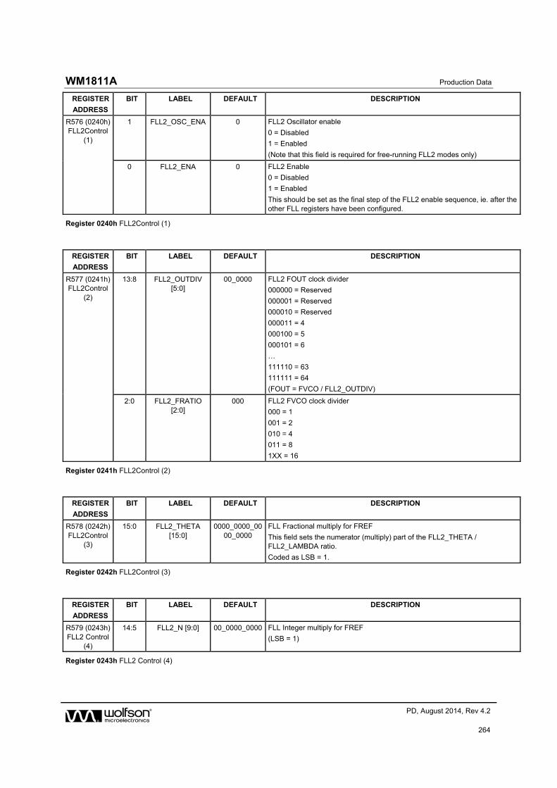
WM1811A Production Data
w PD, August 2014, Rev 4.2
264
REGISTER
ADDRESS
BIT LABEL DEFAULT DESCRIPTION
R576 (0240h) FLL2Control
(1)
1 FLL2_OSC_ENA 0 FLL2 Oscillator enable
0 = Disabled
1 = Enabled
(Note that this field is required for free-running FLL2 modes only)
0 FLL2_ENA 0 FLL2 Enable
0 = Disabled
1 = Enabled
This should be set as the final step of the FLL2 enable sequence, ie. after the other FLL registers have been configured.
Register 0240h FLL2Control (1)
REGISTER
ADDRESS
BIT LABEL DEFAULT DESCRIPTION
R577 (0241h) FLL2Control
(2)
13:8 FLL2_OUTDIV [5:0]
00_0000 FLL2 FOUT clock divider
000000 = Reserved
000001 = Reserved
000010 = Reserved
000011 = 4
000100 = 5
000101 = 6
…
111110 = 63
111111 = 64
(FOUT = FVCO / FLL2_OUTDIV)
2:0 FLL2_FRATIO [2:0]
000 FLL2 FVCO clock divider
000 = 1
001 = 2
010 = 4
011 = 8
1XX = 16
Register 0241h FLL2Control (2)
REGISTER
ADDRESS
BIT LABEL DEFAULT DESCRIPTION
R578 (0242h) FLL2Control
(3)
15:0 FLL2_THETA [15:0]
0000_0000_0000_0000
FLL Fractional multiply for FREF
This field sets the numerator (multiply) part of the FLL2_THETA / FLL2_LAMBDA ratio.
Coded as LSB = 1.
Register 0242h FLL2Control (3)
REGISTER
ADDRESS
BIT LABEL DEFAULT DESCRIPTION
R579 (0243h) FLL2 Control
(4)
14:5 FLL2_N [9:0] 00_0000_0000 FLL Integer multiply for FREF
(LSB = 1)
Register 0243h FLL2 Control (4)

Production Data WM1811A
w PD, August 2014, Rev 4.2
265
REGISTER
ADDRESS
BIT LABEL DEFAULT DESCRIPTION
R580 (0244h) FLL2Control
(5)
15 FLL2_BYP 0 FLL2 Bypass Select
0 = Disabled
1 = Enabled
When FLL2_BYP is set, the FLL2 output is derived directly from BCLK2. In this case, FLL2 can be disabled.
12:7 FLL2_FRC_NCO_VAL [5:0]
01_1001 FLL2 Forced oscillator value
Valid range is 000000 to 111111
0x19h (011001) = 12MHz approx
(Note that this field is required for free-running FLL modes only)
6 FLL2_FRC_NCO 0 FLL2 Forced control select
0 = Normal
1 = FLL2 oscillator controlled by FLL2_FRC_NCO_VAL
(Note that this field is required for free-running FLL modes only)
4:3 FLL2_REFCLK_DIV [1:0]
00 FLL2 Clock Reference Divider
00 = MCLK / 1
01 = MCLK / 2
10 = MCLK / 4
11 = MCLK / 8
MCLK (or other input reference) must be divided down to <=13.5MHz.
For lower power operation, the reference clock can be divided down further if desired.
1:0 FLL2_REFCLK_SRC [1:0]
00 FLL2 Clock source
00 = MCLK1
01 = MCLK2
10 = LRCLK2
11 = BCLK2
Register 0244h FLL2Control (5)
REGISTER
ADDRESS
BIT LABEL DEFAULT DESCRIPTION
R582 (0246h) FLL2 EFS 1
15:0 FLL2_LAMBDA [15:0]
0000_0000_0000_0000
FLL Fractional multiply for FREF
This field sets the denominator (dividing) part of the FLL2_THETA / FLL2_LAMBDA ratio.
Coded as LSB = 1.
Register 0246h FLL2 EFS 1
REGISTER
ADDRESS
BIT LABEL DEFAULT DESCRIPTION
R583 (0247h) FLL2 EFS 2
2 Reserved 1 Reserved - do not change
1 Reserved 1 Reserved - do not change
0 FLL2_EFS_ENA 0 FLL Fractional Mode EFS enable
0 = Integer Mode
1 = Fractional Mode
This bit should be set to 1 when FLL2_THETA > 0.
Register 0247h FLL2 EFS 2

WM1811A Production Data
w PD, August 2014, Rev 4.2
266
REGISTER
ADDRESS
BIT LABEL DEFAULT DESCRIPTION
R768 (0300h) AIF1 Control
(1)
15 AIF1ADCL_SRC 0 AIF1 Left Digital Audio interface source
0 = Left ADC data is output on left channel
1 = Right ADC data is output on left channel
14 AIF1ADCR_SRC 1 AIF1 Right Digital Audio interface source
0 = Left ADC data is output on right channel
1 = Right ADC data is output on right channel
13 AIF1ADC_TDM 0 AIF1 transmit (ADC) TDM Enable
0 = Normal ADCDAT1 operation
1 = TDM enabled on ADCDAT1
12 AIF1ADC_TDM_CHAN
0 AIF1 transmit (ADC) TDM Slot Select
0 = Slot 0
1 = Slot 1
8 AIF1_BCLK_INV 0 BCLK1 Invert
0 = BCLK1 not inverted
1 = BCLK1 inverted
Note that AIF1_BCLK_INV selects the BCLK1 polarity in Master mode and in Slave mode.
6:5 AIF1_WL [1:0] 10 AIF1 Digital Audio Interface Word Length
00 = 16 bits
01 = 20 bits
10 = 24 bits
11 = 32 bits
Note - 8-bit modes can be selected using the “Companding” control bits.
4:3 AIF1_FMT [1:0] 10 AIF1 Digital Audio Interface Format
00 = Right justified
01 = Left justified
10 = I2S Format
11 = DSP Mode
Register 0300h AIF1 Control (1)
REGISTER
ADDRESS
BIT LABEL DEFAULT DESCRIPTION
R769 (0301h) AIF1 Control
(2)
15 AIF1DACL_SRC 0 AIF1 Left Receive Data Source Select
0 = Left DAC receives left interface data
1 = Left DAC receives right interface data
14 AIF1DACR_SRC 1 AIF1 Right Receive Data Source Select
0 = Right DAC receives left interface data
1 = Right DAC receives right interface data
13 AIF1DAC_TDM 0 AIF1 receive (DAC) TDM Enable
0 = Normal DACDAT1 operation
1 = TDM enabled on DACDAT1
12 AIF1DAC_TDM_CHAN
0 AIF1 receive (DAC) TDM Slot Select
0 = Slot 0
1 = Slot 1
11:10 AIF1DAC_BOOST [1:0]
00 AIF1 Input Path Boost
00 = 0dB
01 = +6dB (input must not exceed -6dBFS)
10 = +12dB (input must not exceed -12dBFS)
11 = +18dB (input must not exceed -18dBFS)
8 AIF1_MONO 0 AIF1 DSP Mono Mode
0 = Disabled

Production Data WM1811A
w PD, August 2014, Rev 4.2
267
REGISTER
ADDRESS
BIT LABEL DEFAULT DESCRIPTION
1 = Enabled
Note that Mono Mode is only supported when AIF1_FMT = 11.
4 AIF1DAC_COMP 0 AIF1 Receive Companding Enable
0 = Disabled
1 = Enabled
3 AIF1DAC_COMPMODE
0 AIF1 Receive Companding Type
0 = µ-law
1 = A-law
2 AIF1ADC_COMP 0 AIF1 Transmit Companding Enable
0 = Disabled
1 = Enabled
1 AIF1ADC_COMPMODE
0 AIF1 Transmit Companding Type
0 = µ-law
1 = A-law
0 AIF1_LOOPBACK 0 AIF1 Digital Loopback Function
0 = No loopback
1 = Loopback enabled (ADCDAT1 data output is directly input to DACDAT1 data input).
Register 0301h AIF1 Control (2)
REGISTER
ADDRESS
BIT LABEL DEFAULT DESCRIPTION
R770 (0302h) AIF1 Master/
Slave
15 AIF1_TRI 0 AIF1 Audio Interface tri-state
0 = AIF1 pins operate normally
1 = Tri-state all AIF1 interface pins
Note that the GPIO1 pin is controlled by this register only when configured as ADCLRCLK1.
14 AIF1_MSTR 0 AIF1 Audio Interface Master Mode Select
0 = Slave mode
1 = Master mode
13 AIF1_CLK_FRC 0 Forces BCLK1, LRCLK1 and ADCLRCLK1 to be enabled when all AIF1 audio channels are disabled.
0 = Normal
1 = BCLK1, LRCLK1 and ADCLRCLK1 always enabled in Master mode
12 AIF1_LRCLK_FRC
0 Forces LRCLK1 and ADCLRCLK1 to be enabled when all AIF1 audio channels are disabled.
0 = Normal
1 = LRCLK1 and ADCLRCLK1 always enabled in Master mode
Register 0302h AIF1 Master/Slave
REGISTER
ADDRESS
BIT LABEL DEFAULT DESCRIPTION
R771 (0303h) AIF1 BCLK
8:4 AIF1_BCLK_DIV [4:0]
0_0100 BCLK1 Rate
00000 = AIF1CLK
00001 = AIF1CLK / 1.5
00010 = AIF1CLK / 2
00011 = AIF1CLK / 3
00100 = AIF1CLK / 4
00101 = AIF1CLK / 5
00110 = AIF1CLK / 6

WM1811A Production Data
w PD, August 2014, Rev 4.2
268
REGISTER
ADDRESS
BIT LABEL DEFAULT DESCRIPTION
00111 = AIF1CLK / 8
01000 = AIF1CLK / 11
01001 = AIF1CLK / 12
01010 = AIF1CLK / 16
01011 = AIF1CLK / 22
01100 = AIF1CLK / 24
01101 = AIF1CLK / 32
01110 = AIF1CLK / 44
01111 = AIF1CLK / 48
10000 = AIF1CLK / 64
10001 = AIF1CLK / 88
10010 = AIF1CLK / 96
10011 = AIF1CLK / 128
10100 = AIF1CLK / 176
10101 = AIF1CLK / 192
10110 - 11111 = Reserved
Register 0303h AIF1 BCLK
REGISTER
ADDRESS
BIT LABEL DEFAULT DESCRIPTION
R772 (0304h) AIF1ADC LRCLK
12 AIF1ADC_LRCLK_INV
0 Right, left and I2S modes – ADCLRCLK1 polarity
0 = normal ADCLRCLK1 polarity
1 = invert ADCLRCLK1 polarity
Note that AIF1ADC_LRCLK_INV selects the ADCLRCLK1 polarity in Master mode and in Slave mode.
DSP Mode – mode A/B select
0 = MSB is available on 2nd BCLK1 rising edge after ADCLRCLK1 rising edge (mode A)
1 = MSB is available on 1st BCLK1 rising edge after ADCLRCLK1 rising edge (mode B)
11 AIF1ADC_LRCLK_DIR
0 Allows ADCLRCLK1 to be enabled in Slave mode
0 = Normal
1 = ADCLRCLK1 enabled in Slave mode
10:0 AIF1ADC_RATE [10:0]
000_0100_0000
ADCLRCLK1 Rate
ADCLRCLK1 clock output =
BCLK1 / AIF1ADC_RATE
Integer (LSB = 1)
Valid from 8..2047
Register 0304h AIF1ADC LRCLK
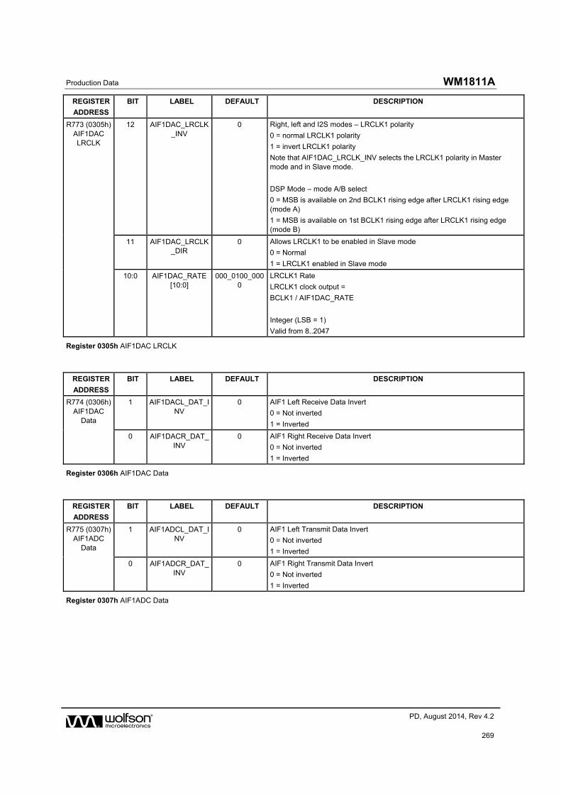
Production Data WM1811A
w PD, August 2014, Rev 4.2
269
REGISTER
ADDRESS
BIT LABEL DEFAULT DESCRIPTION
R773 (0305h) AIF1DAC LRCLK
12 AIF1DAC_LRCLK_INV
0 Right, left and I2S modes – LRCLK1 polarity
0 = normal LRCLK1 polarity
1 = invert LRCLK1 polarity
Note that AIF1DAC_LRCLK_INV selects the LRCLK1 polarity in Master mode and in Slave mode.
DSP Mode – mode A/B select
0 = MSB is available on 2nd BCLK1 rising edge after LRCLK1 rising edge (mode A)
1 = MSB is available on 1st BCLK1 rising edge after LRCLK1 rising edge (mode B)
11 AIF1DAC_LRCLK_DIR
0 Allows LRCLK1 to be enabled in Slave mode
0 = Normal
1 = LRCLK1 enabled in Slave mode
10:0 AIF1DAC_RATE [10:0]
000_0100_0000
LRCLK1 Rate
LRCLK1 clock output =
BCLK1 / AIF1DAC_RATE
Integer (LSB = 1)
Valid from 8..2047
Register 0305h AIF1DAC LRCLK
REGISTER
ADDRESS
BIT LABEL DEFAULT DESCRIPTION
R774 (0306h) AIF1DAC
Data
1 AIF1DACL_DAT_INV
0 AIF1 Left Receive Data Invert
0 = Not inverted
1 = Inverted
0 AIF1DACR_DAT_INV
0 AIF1 Right Receive Data Invert
0 = Not inverted
1 = Inverted
Register 0306h AIF1DAC Data
REGISTER
ADDRESS
BIT LABEL DEFAULT DESCRIPTION
R775 (0307h) AIF1ADC
Data
1 AIF1ADCL_DAT_INV
0 AIF1 Left Transmit Data Invert
0 = Not inverted
1 = Inverted
0 AIF1ADCR_DAT_INV
0 AIF1 Right Transmit Data Invert
0 = Not inverted
1 = Inverted
Register 0307h AIF1ADC Data
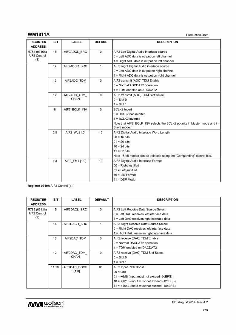
WM1811A Production Data
w PD, August 2014, Rev 4.2
270
REGISTER
ADDRESS
BIT LABEL DEFAULT DESCRIPTION
R784 (0310h) AIF2 Control
(1)
15 AIF2ADCL_SRC 0 AIF2 Left Digital Audio interface source
0 = Left ADC data is output on left channel
1 = Right ADC data is output on left channel
14 AIF2ADCR_SRC 1 AIF2 Right Digital Audio interface source
0 = Left ADC data is output on right channel
1 = Right ADC data is output on right channel
13 AIF2ADC_TDM 0 AIF2 transmit (ADC) TDM Enable
0 = Normal ADCDAT2 operation
1 = TDM enabled on ADCDAT2
12 AIF2ADC_TDM_CHAN
0 AIF2 transmit (ADC) TDM Slot Select
0 = Slot 0
1 = Slot 1
8 AIF2_BCLK_INV 0 BCLK2 Invert
0 = BCLK2 not inverted
1 = BCLK2 inverted
Note that AIF2_BCLK_INV selects the BCLK2 polarity in Master mode and in Slave mode.
6:5 AIF2_WL [1:0] 10 AIF2 Digital Audio Interface Word Length
00 = 16 bits
01 = 20 bits
10 = 24 bits
11 = 32 bits
Note - 8-bit modes can be selected using the “Companding” control bits.
4:3 AIF2_FMT [1:0] 10 AIF2 Digital Audio Interface Format
00 = Right justified
01 = Left justified
10 = I2S Format
11 = DSP Mode
Register 0310h AIF2 Control (1)
REGISTER
ADDRESS
BIT LABEL DEFAULT DESCRIPTION
R785 (0311h) AIF2 Control
(2)
15 AIF2DACL_SRC 0 AIF2 Left Receive Data Source Select
0 = Left DAC receives left interface data
1 = Left DAC receives right interface data
14 AIF2DACR_SRC 1 AIF2 Right Receive Data Source Select
0 = Right DAC receives left interface data
1 = Right DAC receives right interface data
13 AIF2DAC_TDM 0 AIF2 receive (DAC) TDM Enable
0 = Normal DACDAT2 operation
1 = TDM enabled on DACDAT2
12 AIF2DAC_TDM_CHAN
0 AIF2 receive (DAC) TDM Slot Select
0 = Slot 0
1 = Slot 1
11:10 AIF2DAC_BOOST [1:0]
00 AIF2 Input Path Boost
00 = 0dB
01 = +6dB (input must not exceed -6dBFS)
10 = +12dB (input must not exceed -12dBFS)
11 = +18dB (input must not exceed -18dBFS)

Production Data WM1811A
w PD, August 2014, Rev 4.2
271
REGISTER
ADDRESS
BIT LABEL DEFAULT DESCRIPTION
8 AIF2_MONO 0 AIF2 DSP Mono Mode
0 = Disabled
1 = Enabled
Note that Mono Mode is only supported when AIF2_FMT = 11.
4 AIF2DAC_COMP 0 AIF2 Receive Companding Enable
0 = Disabled
1 = Enabled
3 AIF2DAC_COMPMODE
0 AIF2 Receive Companding Type
0 = µ-law
1 = A-law
2 AIF2ADC_COMP 0 AIF2 Transmit Companding Enable
0 = Disabled
1 = Enabled
1 AIF2ADC_COMPMODE
0 AIF2 Transmit Companding Type
0 = µ-law
1 = A-law
0 AIF2_LOOPBACK 0 AIF2 Digital Loopback Function
0 = No loopback
1 = Loopback enabled (ADCDAT2 data output is directly input to DACDAT2 data input).
Register 0311h AIF2 Control (2)
REGISTER
ADDRESS
BIT LABEL DEFAULT DESCRIPTION
R786 (0312h) AIF2 Master/
Slave
15 AIF2_TRI 0 AIF2 Audio Interface tri-state
0 = AIF2 pins operate normally
1 = Tri-state all AIF2 interface pins
Note that pins not configured as AIF2 functions are not affected by this register.
14 AIF2_MSTR 0 AIF2 Audio Interface Master Mode Select
0 = Slave mode
1 = Master mode
13 AIF2_CLK_FRC 0 Forces BCLK2 and LRCLK2 to be enabled when all AIF2 audio channels are disabled.
0 = Normal
1 = BCLK2 and LRCLK2 always enabled in Master mode
12 AIF2_LRCLK_FRC
0 Forces LRCLK2 to be enabled when all AIF2 audio channels are disabled.
0 = Normal
1 = LRCLK2 always enabled in Master mode
Register 0312h AIF2 Master/Slave

WM1811A Production Data
w PD, August 2014, Rev 4.2
272
REGISTER
ADDRESS
BIT LABEL DEFAULT DESCRIPTION
R787 (0313h) AIF2 BCLK
8:4 AIF2_BCLK_DIV [4:0]
0_0100 BCLK2 Rate
00000 = AIF2CLK
00001 = AIF2CLK / 1.5
00010 = AIF2CLK / 2
00011 = AIF2CLK / 3
00100 = AIF2CLK / 4
00101 = AIF2CLK / 5
00110 = AIF2CLK / 6
00111 = AIF2CLK / 8
01000 = AIF2CLK / 11
01001 = AIF2CLK / 12
01010 = AIF2CLK / 16
01011 = AIF2CLK / 22
01100 = AIF2CLK / 24
01101 = AIF2CLK / 32
01110 = AIF2CLK / 44
01111 = AIF2CLK / 48
10000 = AIF2CLK / 64
10001 = AIF2CLK / 88
10010 = AIF2CLK / 96
10011 = AIF2CLK / 128
10100 = AIF2CLK / 176
10101 = AIF2CLK / 192
10110 - 11111 = Reserved
Register 0313h AIF2 BCLK
REGISTER
ADDRESS
BIT LABEL DEFAULT DESCRIPTION
R788 (0314h) AIF2ADC LRCLK
12 AIF2ADC_LRCLK_INV
0 DSP Mode – mode A/B select (AIF2 output)
0 = MSB is available on 2nd BCLK2 rising edge after LRCLK2 rising edge (mode A)
1 = MSB is available on 1st BCLK2 rising edge after LRCLK2 rising edge (mode B)
6 1 Reserved - do not change
Register 0314h AIF2ADC LRCLK
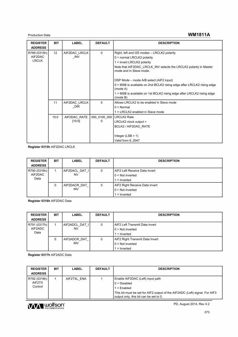
Production Data WM1811A
w PD, August 2014, Rev 4.2
273
REGISTER
ADDRESS
BIT LABEL DEFAULT DESCRIPTION
R789 (0315h) AIF2DAC LRCLK
12 AIF2DAC_LRCLK_INV
0 Right, left and I2S modes – LRCLK2 polarity
0 = normal LRCLK2 polarity
1 = invert LRCLK2 polarity
Note that AIF2DAC_LRCLK_INV selects the LRCLK2 polarity in Master mode and in Slave mode.
DSP Mode – mode A/B select (AIF2 input)
0 = MSB is available on 2nd BCLK2 rising edge after LRCLK2 rising edge (mode A)
1 = MSB is available on 1st BCLK2 rising edge after LRCLK2 rising edge (mode B)
11 AIF2DAC_LRCLK_DIR
0 Allows LRCLK2 to be enabled in Slave mode
0 = Normal
1 = LRCLK2 enabled in Slave mode
10:0 AIF2DAC_RATE [10:0]
000_0100_0000
LRCLK2 Rate
LRCLK2 clock output =
BCLK2 / AIF2DAC_RATE
Integer (LSB = 1)
Valid from 8..2047
Register 0315h AIF2DAC LRCLK
REGISTER
ADDRESS
BIT LABEL DEFAULT DESCRIPTION
R790 (0316h) AIF2DAC
Data
1 AIF2DACL_DAT_INV
0 AIF2 Left Receive Data Invert
0 = Not inverted
1 = Inverted
0 AIF2DACR_DAT_INV
0 AIF2 Right Receive Data Invert
0 = Not inverted
1 = Inverted
Register 0316h AIF2DAC Data
REGISTER
ADDRESS
BIT LABEL DEFAULT DESCRIPTION
R791 (0317h) AIF2ADC
Data
1 AIF2ADCL_DAT_INV
0 AIF2 Left Transmit Data Invert
0 = Not inverted
1 = Inverted
0 AIF2ADCR_DAT_INV
0 AIF2 Right Transmit Data Invert
0 = Not inverted
1 = Inverted
Register 0317h AIF2ADC Data
REGISTER
ADDRESS
BIT LABEL DEFAULT DESCRIPTION
R792 (0318h) AIF2TX Control
1 AIF2TXL_ENA 1 Enable AIF2DAC (Left) input path
0 = Disabled
1 = Enabled
This bit must be set for AIF2 output of the AIF2ADC (Left) signal. For AIF3 output only, this bit can be set to 0.

WM1811A Production Data
w PD, August 2014, Rev 4.2
274
REGISTER
ADDRESS
BIT LABEL DEFAULT DESCRIPTION
0 AIF2TXR_ENA 1 Enable AIF2DAC (Right) input path
0 = Disabled
1 = Enabled
This bit must be set for AIF2 output of the AIF2ADC (Left) signal. For AIF3 output only, this bit can be set to 0.
Register 0318h AIF2TX Control
REGISTER
ADDRESS
BIT LABEL DEFAULT DESCRIPTION
R800 (0320h) AIF3 Control
(1)
7 AIF3_LRCLK_INV 0 Right, left and I2S modes – LRCLK3 polarity
0 = normal LRCLK3 polarity
1 = invert LRCLK3 polarity
DSP Mode – mode A/B select
0 = MSB is available on 2nd BCLK3 rising edge after LRCLK3 rising edge (mode A)
1 = MSB is available on 1st BCLK3 rising edge after LRCLK3 rising edge (mode B)
6:5 AIF3_WL [1:0] 10 AIF3 Digital Audio Interface Word Length
00 = 16 bits
01 = 20 bits
10 = 24 bits
11 = 32 bits
Note - 8-bit modes can be selected using the “Companding” control bits.
Note that this controls the AIF3 Mono PCM interface path only; it does not affect AIF3 inputs/outputs routed to AIF1 or AIF2.
Register 0320h AIF3 Control (1)
REGISTER
ADDRESS
BIT LABEL DEFAULT DESCRIPTION
R801 (0321h) AIF3 Control
(2)
11:10 AIF3DAC_BOOST [1:0]
00 AIF3 Input Path Boost
00 = 0dB
01 = +6dB (input must not exceed -6dBFS)
10 = +12dB (input must not exceed -12dBFS)
11 = +18dB (input must not exceed -18dBFS)
Note that this controls the AIF3 Mono PCM interface path only; it does not affect DACDAT3 input to AIF1 or AIF2.
4 AIF3DAC_COMP 0 AIF3 Receive Companding Enable
0 = Disabled
1 = Enabled
Note that this controls the AIF3 Mono PCM interface path only; it does not affect DACDAT3 input to AIF1 or AIF2.
3 AIF3DAC_COMPMODE
0 AIF3 Receive Companding Type
0 = µ-law
1 = A-law
Note that this controls the AIF3 Mono PCM interface path only; it does not affect DACDAT3 input to AIF1 or AIF2.

Production Data WM1811A
w PD, August 2014, Rev 4.2
275
REGISTER
ADDRESS
BIT LABEL DEFAULT DESCRIPTION
2 AIF3ADC_COMP 0 AIF3 Transmit Companding Enable
0 = Disabled
1 = Enabled
Note that this controls the AIF3 Mono PCM interface path only; it does not affect ADCDAT3 output from AIF1 or AIF2.
1 AIF3ADC_COMPMODE
0 AIF3 Transmit Companding Type
0 = µ-law
1 = A-law
Note that this controls the AIF3 Mono PCM interface path only; it does not affect ADCDAT3 output from AIF1 or AIF2.
0 AIF3_LOOPBACK 0 AIF3 Digital Loopback Function
0 = No loopback
1 = Loopback enabled (AIF3 Mono PCM data output is directly input to AIF3 Mono PCM data input).
Register 0321h AIF3 Control (2)
REGISTER
ADDRESS
BIT LABEL DEFAULT DESCRIPTION
R802 (0322h) AIF3DAC
Data
0 AIF3DAC_DAT_INV
0 AIF3 Receive Data Invert
0 = Not inverted
1 = Inverted
Note that this controls the AIF3 Mono PCM interface path only; it does not affect DACDAT3 input to AIF1 or AIF2.
Register 0322h AIF3DAC Data
REGISTER
ADDRESS
BIT LABEL DEFAULT DESCRIPTION
R803 (0323h) AIF3ADC
Data
0 AIF3ADC_DAT_INV
0 AIF3 Transmit Data Invert
0 = Not inverted
1 = Inverted
Note that this controls the AIF3 Mono PCM interface path only; it does not affect ADCDAT3 output from AIF1 or AIF2.
Register 0323h AIF3ADC Data
REGISTER
ADDRESS
BIT LABEL DEFAULT DESCRIPTION
R1024 (0400h) AIF1
ADC1 Left Volume
8 AIF1ADC1_VU 0 AIF1ADC output path Volume Update
Writing a 1 to this bit will cause the AIF1ADC1L and AIF1ADC1R volume to be updated simultaneously
7:0 AIF1ADC1L_VOL [7:0]
1100_0000 AIF1ADC (Left) output path Digital Volume
00h = MUTE
01h = -71.625dB
… (0.375dB steps)
EFh = +17.625dB
Register 0400h AIF1 ADC1 Left Volume

WM1811A Production Data
w PD, August 2014, Rev 4.2
276
REGISTER
ADDRESS
BIT LABEL DEFAULT DESCRIPTION
R1025 (0401h) AIF1 ADC1 Right
Volume
8 AIF1ADC1_VU 0 AIF1ADC output path Volume Update
Writing a 1 to this bit will cause the AIF1ADC1L and AIF1ADC1R volume to be updated simultaneously
7:0 AIF1ADC1R_VOL [7:0]
1100_0000 AIF1ADC (Right) output path Digital Volume
00h = MUTE
01h = -71.625dB
… (0.375dB steps)
EFh = +17.625dB
Register 0401h AIF1 ADC1 Right Volume
REGISTER
ADDRESS
BIT LABEL DEFAULT DESCRIPTION
R1026 (0402h) AIF1
DAC1 Left Volume
8 AIF1DAC1_VU 0 AIF1DAC input path Volume Update
Writing a 1 to this bit will cause the AIF1DAC1L and AIF1DAC1R volume to be updated simultaneously
7:0 AIF1DAC1L_VOL [7:0]
1100_0000 AIF1DAC (Left) input path Digital Volume
00h = MUTE
01h = -71.625dB
… (0.375dB steps)
C0h = 0dB
FFh = 0dB
Register 0402h AIF1 DAC1 Left Volume
REGISTER
ADDRESS
BIT LABEL DEFAULT DESCRIPTION
R1027 (0403h) AIF1 DAC1 Right
Volume
8 AIF1DAC1_VU 0 AIF1DAC input path Volume Update
Writing a 1 to this bit will cause the AIF1DAC1L and AIF1DAC1R volume to be updated simultaneously
7:0 AIF1DAC1R_VOL [7:0]
1100_0000 AIF1DAC (Right) input path Digital Volume
00h = MUTE
01h = -71.625dB
… (0.375dB steps)
C0h = 0dB
FFh = 0dB
Register 0403h AIF1 DAC1 Right Volume
REGISTER
ADDRESS
BIT LABEL DEFAULT DESCRIPTION
R1040 (0410h) AIF1 ADC1 Filters
15 AIF1ADC_4FS 0 Enable AIF1ADC ultrasonic mode (4FS) output, bypassing all AIF1 baseband output filtering
0 = Disabled
1 = Enabled
14:13 AIF1ADC1_HPF_CUT [1:0]
00 AIF1ADC output path Digital HPF cut-off frequency (fc)
00 = Hi-fi mode (fc = 4Hz at fs = 48kHz)
01 = Voice mode 1 (fc = 64Hz at fs = 8kHz)
10 = Voice mode 2 (fc = 130Hz at fs = 8kHz)
11 = Voice mode 3 (fc = 267Hz at fs = 8kHz)

Production Data WM1811A
w PD, August 2014, Rev 4.2
277
REGISTER
ADDRESS
BIT LABEL DEFAULT DESCRIPTION
12 AIF1ADC1L_HPF 0 AIF1ADC (Left) output path Digital HPF Enable
0 = Disabled
1 = Enabled
11 AIF1ADC1R_HPF 0 AIF1ADC (Right) output path Digital HPF Enable
0 = Disabled
1 = Enabled
Register 0410h AIF1 ADC1 Filters
REGISTER
ADDRESS
BIT LABEL DEFAULT DESCRIPTION
R1056 (0420h) AIF1 DAC1 Filters
(1)
9 AIF1DAC1_MUTE 1 AIF1DAC input path Soft Mute Control
0 = Un-mute
1 = Mute
7 AIF1DAC1_MONO
0 AIF1DAC input path Mono Mix Control
0 = Disabled
1 = Enabled
5 AIF1DAC1_MUTERATE
0 AIF1DAC input path Soft Mute Ramp Rate
0 = Fast ramp (fs/2, maximum ramp time is 10.7ms at fs=48k)
1 = Slow ramp (fs/32, maximum ramp time is 171ms at fs=48k)
(Note: ramp rate scales with sample rate.)
4 AIF1DAC1_UNMUTE_RAMP
0 AIF1DAC input path Unmute Ramp select
0 = Unmuting the AIF1DAC path (AIF1DAC1_MUTE=0) will immediately apply the AIF1DAC1L_VOL and AIF1DAC1R_VOL settings.
1 = Unmuting the AIF1DAC path (AIF1DAC1_MUTE=0) will cause a gradual volume ramp up to the AIF1DAC1L_VOL and AIF1DAC1R_VOL settings.
Register 0420h AIF1 DAC1 Filters (1)
REGISTER
ADDRESS
BIT LABEL DEFAULT DESCRIPTION
R1057 (0421h) AIF1 DAC1 Filters
(2)
13:9 AIF1DAC1_3D_GAIN [4:0]
0_0000 AIF1DAC playback path 3D Stereo depth
00000 = Off
00001 = Minimum (-16dB)
…(0.915dB steps)
11111 = Maximum (+11.45dB)
8 AIF1DAC1_3D_ENA
0 Enable 3D Stereo in AIF1DAC playback path
0 = Disabled
1 = Enabled
Register 0421h AIF1 DAC1 Filters (2)
REGISTER
ADDRESS
BIT LABEL DEFAULT DESCRIPTION
R1072 (0430h) AIF1 DAC1 Noise
Gate
6:5 AIF1DAC1_NG_HLD [1:0]
11 AIF1DAC input path Noise Gate Hold Time
(delay before noise gate is activated)
00 = 30ms
01 = 125ms
10 = 250ms
11 = 500ms
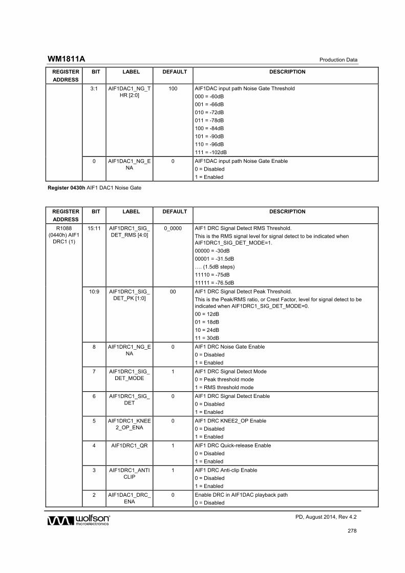
WM1811A Production Data
w PD, August 2014, Rev 4.2
278
REGISTER
ADDRESS
BIT LABEL DEFAULT DESCRIPTION
3:1 AIF1DAC1_NG_THR [2:0]
100 AIF1DAC input path Noise Gate Threshold
000 = -60dB
001 = -66dB
010 = -72dB
011 = -78dB
100 = -84dB
101 = -90dB
110 = -96dB
111 = -102dB
0 AIF1DAC1_NG_ENA
0 AIF1DAC input path Noise Gate Enable
0 = Disabled
1 = Enabled
Register 0430h AIF1 DAC1 Noise Gate
REGISTER
ADDRESS
BIT LABEL DEFAULT DESCRIPTION
R1088 (0440h) AIF1
DRC1 (1)
15:11 AIF1DRC1_SIG_DET_RMS [4:0]
0_0000 AIF1 DRC Signal Detect RMS Threshold.
This is the RMS signal level for signal detect to be indicated when AIF1DRC1_SIG_DET_MODE=1.
00000 = -30dB
00001 = -31.5dB
…. (1.5dB steps)
11110 = -75dB
11111 = -76.5dB
10:9 AIF1DRC1_SIG_DET_PK [1:0]
00 AIF1 DRC Signal Detect Peak Threshold.
This is the Peak/RMS ratio, or Crest Factor, level for signal detect to be indicated when AIF1DRC1_SIG_DET_MODE=0.
00 = 12dB
01 = 18dB
10 = 24dB
11 = 30dB
8 AIF1DRC1_NG_ENA
0 AIF1 DRC Noise Gate Enable
0 = Disabled
1 = Enabled
7 AIF1DRC1_SIG_DET_MODE
1 AIF1 DRC Signal Detect Mode
0 = Peak threshold mode
1 = RMS threshold mode
6 AIF1DRC1_SIG_DET
0 AIF1 DRC Signal Detect Enable
0 = Disabled
1 = Enabled
5 AIF1DRC1_KNEE2_OP_ENA
0 AIF1 DRC KNEE2_OP Enable
0 = Disabled
1 = Enabled
4 AIF1DRC1_QR 1 AIF1 DRC Quick-release Enable
0 = Disabled
1 = Enabled
3 AIF1DRC1_ANTICLIP
1 AIF1 DRC Anti-clip Enable
0 = Disabled
1 = Enabled
2 AIF1DAC1_DRC_ENA
0 Enable DRC in AIF1DAC playback path
0 = Disabled

Production Data WM1811A
w PD, August 2014, Rev 4.2
279
REGISTER
ADDRESS
BIT LABEL DEFAULT DESCRIPTION
1 = Enabled
1 AIF1ADC1L_DRC_ENA
0 Enable DRC in AIF1ADC (Left) record path
0 = Disabled
1 = Enabled
0 AIF1ADC1R_DRC_ENA
0 Enable DRC in AIF1ADC (Right) record path
0 = Disabled
1 = Enabled
Register 0440h AIF1 DRC1 (1)
REGISTER
ADDRESS
BIT LABEL DEFAULT DESCRIPTION
R1089 (0441h) AIF1
DRC1 (2)
12:9 AIF1DRC1_ATK [3:0]
0100 AIF1 DRC Gain attack rate (seconds/6dB)
0000 = Reserved
0001 = 181us
0010 = 363us
0011 = 726us
0100 = 1.45ms
0101 = 2.9ms
0110 = 5.8ms
0111 = 11.6ms
1000 = 23.2ms
1001 = 46.4ms
1010 = 92.8ms
1011 = 185.6ms
1100-1111 = Reserved
8:5 AIF1DRC1_DCY [3:0]
0010 AIF1 DRC Gain decay rate (seconds/6dB)
0000 = 186ms
0001 = 372ms
0010 = 743ms
0011 = 1.49s
0100 = 2.97s
0101 = 5.94s
0110 = 11.89s
0111 = 23.78s
1000 = 47.56s
1001-1111 = Reserved
4:2 AIF1DRC1_MINGAIN [2:0]
001 AIF1 DRC Minimum gain to attenuate audio signals
000 = 0dB
001 = -12dB (default)
010 = -18dB
011 = -24dB
100 = -36dB
101 = Reserved
11X = Reserved
1:0 AIF1DRC1_MAXGAIN [1:0]
01 AIF1 DRC Maximum gain to boost audio signals (dB)
00 = 12dB
01 = 18dB
10 = 24dB
11 = 36dB
Register 0441h AIF1 DRC1 (2)

WM1811A Production Data
w PD, August 2014, Rev 4.2
280
REGISTER
ADDRESS
BIT LABEL DEFAULT DESCRIPTION
R1090 (0442h) AIF1
DRC1 (3)
15:12 AIF1DRC1_NG_MINGAIN [3:0]
0000 AIF1 DRC Minimum gain to attenuate audio signals when the noise gate is active.
0000 = -36dB
0001 = -30dB
0010 = -24dB
0011 = -18dB
0100 = -12dB
0101 = -6dB
0110 = 0dB
0111 = 6dB
1000 = 12dB
1001 = 18dB
1010 = 24dB
1011 = 30dB
1100 = 36dB
1101 to 1111 = Reserved
11:10 AIF1DRC1_NG_EXP [1:0]
00 AIF1 DRC Noise Gate slope
00 = 1 (no expansion)
01 = 2
10 = 4
11 = 8
9:8 AIF1DRC1_QR_THR [1:0]
00 AIF1 DRC Quick-release threshold (crest factor in dB)
00 = 12dB
01 = 18dB
10 = 24dB
11 = 30dB
7:6 AIF1DRC1_QR_DCY [1:0]
00 AIF1 DRC Quick-release decay rate (seconds/6dB)
00 = 0.725ms
01 = 1.45ms
10 = 5.8ms
11 = Reserved
5:3 AIF1DRC1_HI_COMP [2:0]
000 AIF1 DRC Compressor slope (upper region)
000 = 1 (no compression)
001 = 1/2
010 = 1/4
011 = 1/8
100 = 1/16
101 = 0
110 = Reserved
111 = Reserved
2:0 AIF1DRC1_LO_COMP [2:0]
000 AIF1 DRC Compressor slope (lower region)
000 = 1 (no compression) 001 = 1/2 010 = 1/4 011 = 1/8 100 = 0 101 = Reserved 11X = Reserved
Register 0442h AIF1 DRC1 (3)

Production Data WM1811A
w PD, August 2014, Rev 4.2
281
REGISTER
ADDRESS
BIT LABEL DEFAULT DESCRIPTION
R1091 (0443h) AIF1
DRC1 (4)
10:5 AIF1DRC1_KNEE_IP [5:0]
00_0000 AIF1 DRC Input signal level at the Compressor ‘Knee’.
000000 = 0dB
000001 = -0.75dB
000010 = -1.5dB
… (-0.75dB steps)
111100 = -45dB
111101 = Reserved
11111X = Reserved
4:0 AIF1DRC1_KNEE_OP [4:0]
0_0000 AIF1 DRC Output signal at the Compressor ‘Knee’.
00000 = 0dB
00001 = -0.75dB
00010 = -1.5dB
… (-0.75dB steps)
11110 = -22.5dB
11111 = Reserved
Register 0443h AIF1 DRC1 (4)
REGISTER
ADDRESS
BIT LABEL DEFAULT DESCRIPTION
R1092 (0444h) AIF1
DRC1 (5)
9:5 AIF1DRC1_KNEE2_IP [4:0]
0_0000 AIF1 DRC Input signal level at the Noise Gate threshold ‘Knee2’.
00000 = -36dB
00001 = -37.5dB
00010 = -39dB
… (-1.5dB steps)
11110 = -81dB
11111 = -82.5dB
Only applicable when AIF1DRC1_NG_ENA = 1.
4:0 AIF1DRC1_KNEE2_OP [4:0]
0_0000 AIF1 DRC Output signal at the Noise Gate threshold ‘Knee2’.
00000 = -30dB
00001 = -31.5dB
00010 = -33dB
… (-1.5dB steps)
11110 = -75dB
11111 = -76.5dB
Only applicable when AIF1DRC1_KNEE2_OP_ENA = 1.
Register 0444h AIF1 DRC1 (5)
REGISTER
ADDRESS
BIT LABEL DEFAULT DESCRIPTION
R1152 (0480h) AIF1
DAC1 EQ Gains (1)
15:11 AIF1DAC1_EQ_B1_GAIN [4:0]
0_1100 AIF1 EQ Band 1 Gain
-12dB to +12dB in 1dB steps
10:6 AIF1DAC1_EQ_B2_GAIN [4:0]
0_1100 AIF1 EQ Band 2 Gain
-12dB to +12dB in 1dB steps
5:1 AIF1DAC1_EQ_B3_GAIN [4:0]
0_1100 AIF1 EQ Band 3 Gain
-12dB to +12dB in 1dB steps
0 AIF1DAC1_EQ_ENA
0 Enable EQ in AIF1DAC playback path
0 = Disabled
1 = Enabled
Register 0480h AIF1 DAC1 EQ Gains (1)

WM1811A Production Data
w PD, August 2014, Rev 4.2
282
REGISTER
ADDRESS
BIT LABEL DEFAULT DESCRIPTION
R1153 (0481h) AIF1
DAC1 EQ Gains (2)
15:11 AIF1DAC1_EQ_B4_GAIN [4:0]
0_1100 AIF1 EQ Band 4 Gain
-12dB to +12dB in 1dB steps
10:6 AIF1DAC1_EQ_B5_GAIN [4:0]
0_1100 AIF1 EQ Band 5 Gain
-12dB to +12dB in 1dB steps
0 AIF1DAC1_EQ_MODE
0 AIF1 EQ Band 1 Mode
0 = Shelving filter
1 = Peak filter
Register 0481h AIF1 DAC1 EQ Gains (2)
REGISTER
ADDRESS
BIT LABEL DEFAULT DESCRIPTION
R1154 (0482h) AIF1
DAC1 EQ Band 1 A
15:0 AIF1DAC1_EQ_B1_A [15:0]
0000_1111_1100_1010
EQ Band 1 Coefficient A
Register 0482h AIF1 DAC1 EQ Band 1 A
REGISTER
ADDRESS
BIT LABEL DEFAULT DESCRIPTION
R1155 (0483h) AIF1
DAC1 EQ Band 1 B
15:0 AIF1DAC1_EQ_B1_B [15:0]
0000_0100_0000_0000
EQ Band 1 Coefficient B
Register 0483h AIF1 DAC1 EQ Band 1 B
REGISTER
ADDRESS
BIT LABEL DEFAULT DESCRIPTION
R1156 (0484h) AIF1
DAC1 EQ Band 1 PG
15:0 AIF1DAC1_EQ_B1_PG [15:0]
0000_0000_1101_1000
EQ Band 1 Coefficient PG
Register 0484h AIF1 DAC1 EQ Band 1 PG
REGISTER
ADDRESS
BIT LABEL DEFAULT DESCRIPTION
R1157 (0485h) AIF1
DAC1 EQ Band 2 A
15:0 AIF1DAC1_EQ_B2_A [15:0]
0001_1110_1011_0101
EQ Band 2 Coefficient A
Register 0485h AIF1 DAC1 EQ Band 2 A

Production Data WM1811A
w PD, August 2014, Rev 4.2
283
REGISTER
ADDRESS
BIT LABEL DEFAULT DESCRIPTION
R1158 (0486h) AIF1
DAC1 EQ Band 2 B
15:0 AIF1DAC1_EQ_B2_B [15:0]
1111_0001_0100_0101
EQ Band 2 Coefficient B
Register 0486h AIF1 DAC1 EQ Band 2 B
REGISTER
ADDRESS
BIT LABEL DEFAULT DESCRIPTION
R1159 (0487h) AIF1
DAC1 EQ Band 2 C
15:0 AIF1DAC1_EQ_B2_C [15:0]
0000_1011_0111_0101
EQ Band 2 Coefficient C
Register 0487h AIF1 DAC1 EQ Band 2 C
REGISTER
ADDRESS
BIT LABEL DEFAULT DESCRIPTION
R1160 (0488h) AIF1
DAC1 EQ Band 2 PG
15:0 AIF1DAC1_EQ_B2_PG [15:0]
0000_0001_1100_0101
EQ Band 2 Coefficient PG
Register 0488h AIF1 DAC1 EQ Band 2 PG
REGISTER
ADDRESS
BIT LABEL DEFAULT DESCRIPTION
R1161 (0489h) AIF1
DAC1 EQ Band 3 A
15:0 AIF1DAC1_EQ_B3_A [15:0]
0001_1100_0101_1000
EQ Band 3 Coefficient A
Register 0489h AIF1 DAC1 EQ Band 3 A
REGISTER
ADDRESS
BIT LABEL DEFAULT DESCRIPTION
R1162 (048Ah) AIF1
DAC1 EQ Band 3 B
15:0 AIF1DAC1_EQ_B3_B [15:0]
1111_0011_0111_0011
EQ Band 3 Coefficient B
Register 048Ah AIF1 DAC1 EQ Band 3 B
REGISTER
ADDRESS
BIT LABEL DEFAULT DESCRIPTION
R1163 (048Bh) AIF1
DAC1 EQ Band 3 C
15:0 AIF1DAC1_EQ_B3_C [15:0]
0000_1010_0101_0100
EQ Band 3 Coefficient C
Register 048Bh AIF1 DAC1 EQ Band 3 C

WM1811A Production Data
w PD, August 2014, Rev 4.2
284
REGISTER
ADDRESS
BIT LABEL DEFAULT DESCRIPTION
R1164 (048Ch) AIF1
DAC1 EQ Band 3 PG
15:0 AIF1DAC1_EQ_B3_PG [15:0]
0000_0101_0101_1000
EQ Band 3 Coefficient PG
Register 048Ch AIF1 DAC1 EQ Band 3 PG
REGISTER
ADDRESS
BIT LABEL DEFAULT DESCRIPTION
R1165 (048Dh) AIF1
DAC1 EQ Band 4 A
15:0 AIF1DAC1_EQ_B4_A [15:0]
0001_0110_1000_1110
EQ Band 4 Coefficient A
Register 048Dh AIF1 DAC1 EQ Band 4 A
REGISTER
ADDRESS
BIT LABEL DEFAULT DESCRIPTION
R1166 (048Eh) AIF1
DAC1 EQ Band 4 B
15:0 AIF1DAC1_EQ_B4_B [15:0]
1111_1000_0010_1001
EQ Band 4 Coefficient B
Register 048Eh AIF1 DAC1 EQ Band 4 B
REGISTER
ADDRESS
BIT LABEL DEFAULT DESCRIPTION
R1167 (048Fh) AIF1
DAC1 EQ Band 4 C
15:0 AIF1DAC1_EQ_B4_C [15:0]
0000_0111_1010_1101
EQ Band 4 Coefficient C
Register 048Fh AIF1 DAC1 EQ Band 4 C
REGISTER
ADDRESS
BIT LABEL DEFAULT DESCRIPTION
R1168 (0490h) AIF1
DAC1 EQ Band 4 PG
15:0 AIF1DAC1_EQ_B4_PG [15:0]
0001_0001_0000_0011
EQ Band 4 Coefficient PG
Register 0490h AIF1 DAC1 EQ Band 4 PG
REGISTER
ADDRESS
BIT LABEL DEFAULT DESCRIPTION
R1169 (0491h) AIF1
DAC1 EQ Band 5 A
15:0 AIF1DAC1_EQ_B5_A [15:0]
0000_0101_0110_0100
EQ Band 5 Coefficient A
Register 0491h AIF1 DAC1 EQ Band 5 A

Production Data WM1811A
w PD, August 2014, Rev 4.2
285
REGISTER
ADDRESS
BIT LABEL DEFAULT DESCRIPTION
R1170 (0492h) AIF1
DAC1 EQ Band 5 B
15:0 AIF1DAC1_EQ_B5_B [15:0]
0000_0101_0101_1001
EQ Band 5 Coefficient B
Register 0492h AIF1 DAC1 EQ Band 5 B
REGISTER
ADDRESS
BIT LABEL DEFAULT DESCRIPTION
R1171 (0493h) AIF1
DAC1 EQ Band 5 PG
15:0 AIF1DAC1_EQ_B5_PG [15:0]
0100_0000_0000_0000
EQ Band 5 Coefficient PG
Register 0493h AIF1 DAC1 EQ Band 5 PG
REGISTER
ADDRESS
BIT LABEL DEFAULT DESCRIPTION
R1172 (0494h) AIF1
DAC1 EQ Band 1 C
15:0 AIF1DAC1_EQ_B1_C [15:0]
0000_0000_0000_0000
EQ Band 1 Coefficient C
Register 0494h AIF1 DAC1 EQ Band 1 C
REGISTER
ADDRESS
BIT LABEL DEFAULT DESCRIPTION
R1280 (0500h) AIF2
ADC Left Volume
8 AIF2ADC_VU 0 AIF2ADC output path Volume Update
Writing a 1 to this bit will cause the AIF2ADCL and AIF2ADCR volume to be updated simultaneously
7:0 AIF2ADCL_VOL [7:0]
1100_0000 AIF2ADC (Left) output path Digital Volume
00h = MUTE
01h = -71.625dB
… (0.375dB steps)
EFh = +17.625dB
Register 0500h AIF2 ADC Left Volume
REGISTER
ADDRESS
BIT LABEL DEFAULT DESCRIPTION
R1281 (0501h) AIF2 ADC Right
Volume
8 AIF2ADC_VU 0 AIF2ADC output path Volume Update
Writing a 1 to this bit will cause the AIF2ADCL and AIF2ADCR volume to be updated simultaneously
7:0 AIF2ADCR_VOL [7:0]
1100_0000 AIF2ADC (Right) output path Digital Volume
00h = MUTE
01h = -71.625dB
… (0.375dB steps)
EFh = +17.625dB
Register 0501h AIF2 ADC Right Volume
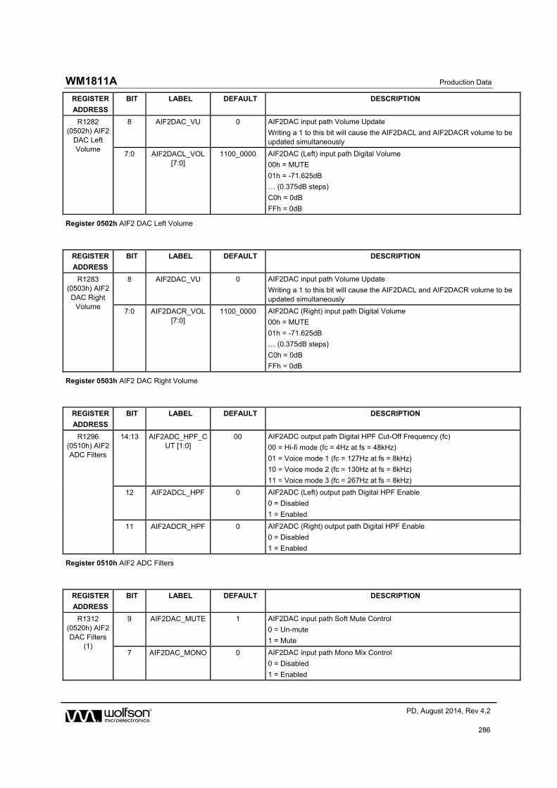
WM1811A Production Data
w PD, August 2014, Rev 4.2
286
REGISTER
ADDRESS
BIT LABEL DEFAULT DESCRIPTION
R1282 (0502h) AIF2
DAC Left Volume
8 AIF2DAC_VU 0 AIF2DAC input path Volume Update
Writing a 1 to this bit will cause the AIF2DACL and AIF2DACR volume to be updated simultaneously
7:0 AIF2DACL_VOL [7:0]
1100_0000 AIF2DAC (Left) input path Digital Volume
00h = MUTE
01h = -71.625dB
… (0.375dB steps)
C0h = 0dB
FFh = 0dB
Register 0502h AIF2 DAC Left Volume
REGISTER
ADDRESS
BIT LABEL DEFAULT DESCRIPTION
R1283 (0503h) AIF2 DAC Right
Volume
8 AIF2DAC_VU 0 AIF2DAC input path Volume Update
Writing a 1 to this bit will cause the AIF2DACL and AIF2DACR volume to be updated simultaneously
7:0 AIF2DACR_VOL [7:0]
1100_0000 AIF2DAC (Right) input path Digital Volume
00h = MUTE
01h = -71.625dB
… (0.375dB steps)
C0h = 0dB
FFh = 0dB
Register 0503h AIF2 DAC Right Volume
REGISTER
ADDRESS
BIT LABEL DEFAULT DESCRIPTION
R1296 (0510h) AIF2 ADC Filters
14:13 AIF2ADC_HPF_CUT [1:0]
00 AIF2ADC output path Digital HPF Cut-Off Frequency (fc)
00 = Hi-fi mode (fc = 4Hz at fs = 48kHz)
01 = Voice mode 1 (fc = 127Hz at fs = 8kHz)
10 = Voice mode 2 (fc = 130Hz at fs = 8kHz)
11 = Voice mode 3 (fc = 267Hz at fs = 8kHz)
12 AIF2ADCL_HPF 0 AIF2ADC (Left) output path Digital HPF Enable
0 = Disabled
1 = Enabled
11 AIF2ADCR_HPF 0 AIF2ADC (Right) output path Digital HPF Enable
0 = Disabled
1 = Enabled
Register 0510h AIF2 ADC Filters
REGISTER
ADDRESS
BIT LABEL DEFAULT DESCRIPTION
R1312 (0520h) AIF2 DAC Filters
(1)
9 AIF2DAC_MUTE 1 AIF2DAC input path Soft Mute Control
0 = Un-mute
1 = Mute
7 AIF2DAC_MONO 0 AIF2DAC input path Mono Mix Control
0 = Disabled
1 = Enabled

Production Data WM1811A
w PD, August 2014, Rev 4.2
287
REGISTER
ADDRESS
BIT LABEL DEFAULT DESCRIPTION
5 AIF2DAC_MUTERATE
0 AIF2DAC input path Soft Mute Ramp Rate
0 = Fast ramp (fs/2, maximum ramp time is 10.7ms at fs=48k)
1 = Slow ramp (fs/32, maximum ramp time is 171ms at fs=48k)
(Note: ramp rate scales with sample rate.)
4 AIF2DAC_UNMUTE_RAMP
0 AIF2DAC input path Unmute Ramp select
0 = Unmuting the AIF2DAC path (AIF2DAC_MUTE=0) will immediately apply the AIF2DACL_VOL and AIF2DACR_VOL settings.
1 = Unmuting the AIF2DAC path (AIF2DAC_MUTE=0) will cause a gradual volume ramp up to the AIF2DACL_VOL and AIF2DACR_VOL settings.
Register 0520h AIF2 DAC Filters (1)
REGISTER
ADDRESS
BIT LABEL DEFAULT DESCRIPTION
R1313 (0521h) AIF2 DAC Filters
(2)
13:9 AIF2DAC_3D_GAIN [4:0]
0_0000 AIF2DAC playback path 3D Stereo depth
00000 = Off
00001 = Minimum (-16dB)
…(0.915dB steps)
11111 = Maximum (+11.45dB)
8 AIF2DAC_3D_ENA
0 Enable 3D Stereo in AIF2DAC playback path
0 = Disabled
1 = Enabled
Register 0521h AIF2 DAC Filters (2)
REGISTER
ADDRESS
BIT LABEL DEFAULT DESCRIPTION
R1328 (0530h) AIF2 DAC Noise
Gate
6:5 AIF2DAC_NG_HLD [1:0]
11 AIF2DAC input path Noise Gate Hold Time
(delay before noise gate is activated)
00 = 30ms
01 = 125ms
10 = 250ms
11 = 500ms
3:1 AIF2DAC_NG_THR [2:0]
100 AIF2DAC input path Noise Gate Threshold
000 = -60dB
001 = -66dB
010 = -72dB
011 = -78dB
100 = -84dB
101 = -90dB
110 = -96dB
111 = -102dB
0 AIF2DAC_NG_ENA
0 AIF2DAC input path Noise Gate Enable
0 = Disabled
1 = Enabled
Register 0530h AIF2 DAC Noise Gate

WM1811A Production Data
w PD, August 2014, Rev 4.2
288
REGISTER
ADDRESS
BIT LABEL DEFAULT DESCRIPTION
R1344 (0540h) AIF2
DRC (1)
15:11 AIF2DRC_SIG_DET_RMS [4:0]
0_0000 AIF2 DRC Signal Detect RMS Threshold.
This is the RMS signal level for signal detect to be indicated when AIF2DRC_SIG_DET_MODE=1.
00000 = -30dB
00001 = -31.5dB
…. (1.5dB steps)
11110 = -75dB
11111 = -76.5dB
10:9 AIF2DRC_SIG_DET_PK [1:0]
00 AIF2 DRC Signal Detect Peak Threshold.
This is the Peak/RMS ratio, or Crest Factor, level for signal detect to be indicated when AIF2DRC_SIG_DET_MODE=0.
00 = 12dB
01 = 18dB
10 = 24dB
11 = 30dB
8 AIF2DRC_NG_ENA
0 AIF2 DRC Noise Gate Enable
0 = Disabled
1 = Enabled
7 AIF2DRC_SIG_DET_MODE
1 AIF2 DRC Signal Detect Mode
0 = Peak threshold mode
1 = RMS threshold mode
6 AIF2DRC_SIG_DET
0 AIF2 DRC Signal Detect Enable
0 = Disabled
1 = Enabled
5 AIF2DRC_KNEE2_OP_ENA
0 AIF2 DRC KNEE2_OP Enable
0 = Disabled
1 = Enabled
4 AIF2DRC_QR 1 AIF2 DRC Quick-release Enable
0 = Disabled
1 = Enabled
3 AIF2DRC_ANTICLIP
1 AIF2 DRC Anti-clip Enable
0 = Disabled
1 = Enabled
2 AIF2DAC_DRC_ENA
0 Enable DRC in AIF2DAC playback path
0 = Disabled
1 = Enabled
1 AIF2ADCL_DRC_ENA
0 Enable DRC in AIF2ADC (Left) record path
0 = Disabled
1 = Enabled
0 AIF2ADCR_DRC_ENA
0 Enable DRC in AIF2ADC (Right) record path
0 = Disabled
1 = Enabled
Register 0540h AIF2 DRC (1)

Production Data WM1811A
w PD, August 2014, Rev 4.2
289
REGISTER
ADDRESS
BIT LABEL DEFAULT DESCRIPTION
R1345 (0541h) AIF2
DRC (2)
12:9 AIF2DRC_ATK [3:0]
0100 AIF2 DRC Gain attack rate (seconds/6dB)
0000 = Reserved
0001 = 181us
0010 = 363us
0011 = 726us
0100 = 1.45ms
0101 = 2.9ms
0110 = 5.8ms
0111 = 11.6ms
1000 = 23.2ms
1001 = 46.4ms
1010 = 92.8ms
1011 = 185.6ms
1100-1111 = Reserved
8:5 AIF2DRC_DCY [3:0]
0010 AIF2 DRC Gain decay rate (seconds/6dB)
0000 = 186ms
0001 = 372ms
0010 = 743ms
0011 = 1.49s
0100 = 2.97s
0101 = 5.94s
0110 = 11.89s
0111 = 23.78s
1000 = 47.56s
1001-1111 = Reserved
4:2 AIF2DRC_MINGAIN [2:0]
001 AIF2 DRC Minimum gain to attenuate audio signals
000 = 0dB
001 = -12dB (default)
010 = -18dB
011 = -24dB
100 = -36dB
101 = Reserved
11X = Reserved
1:0 AIF2DRC_MAXGAIN [1:0]
01 AIF2 DRC Maximum gain to boost audio signals (dB)
00 = 12dB
01 = 18dB
10 = 24dB
11 = 36dB
Register 0541h AIF2 DRC (2)
REGISTER
ADDRESS
BIT LABEL DEFAULT DESCRIPTION
R1346 (0542h) AIF2
DRC (3)
15:12 AIF2DRC_NG_MINGAIN [3:0]
0000 AIF2 DRC Minimum gain to attenuate audio signals when the noise gate is active.
0000 = -36dB
0001 = -30dB
0010 = -24dB
0011 = -18dB
0100 = -12dB
0101 = -6dB
0110 = 0dB

WM1811A Production Data
w PD, August 2014, Rev 4.2
290
REGISTER
ADDRESS
BIT LABEL DEFAULT DESCRIPTION
0111 = 6dB
1000 = 12dB
1001 = 18dB
1010 = 24dB
1011 = 30dB
1100 = 36dB
1101 to 1111 = Reserved
11:10 AIF2DRC_NG_EXP [1:0]
00 AIF2 DRC Noise Gate slope
00 = 1 (no expansion)
01 = 2
10 = 4
11 = 8
9:8 AIF2DRC_QR_THR [1:0]
00 AIF2 DRC Quick-release threshold (crest factor in dB)
00 = 12dB
01 = 18dB
10 = 24dB
11 = 30dB
7:6 AIF2DRC_QR_DCY [1:0]
00 AIF2 DRC Quick-release decay rate (seconds/6dB)
00 = 0.725ms
01 = 1.45ms
10 = 5.8ms
11 = Reserved
5:3 AIF2DRC_HI_COMP [2:0]
000 AIF2 DRC Compressor slope (upper region)
000 = 1 (no compression)
001 = 1/2
010 = 1/4
011 = 1/8
100 = 1/16
101 = 0
110 = Reserved
111 = Reserved
2:0 AIF2DRC_LO_COMP [2:0]
000 AIF2 DRC Compressor slope (lower region)
000 = 1 (no compression)
001 = 1/2
010 = 1/4
011 = 1/8
100 = 0
101 = Reserved
11X = Reserved
Register 0542h AIF2 DRC (3)
REGISTER
ADDRESS
BIT LABEL DEFAULT DESCRIPTION
R1347 (0543h) AIF2
DRC (4)
10:5 AIF2DRC_KNEE_IP [5:0]
00_0000 AIF2 DRC Input signal level at the Compressor ‘Knee’.
000000 = 0dB
000001 = -0.75dB
000010 = -1.5dB
… (-0.75dB steps)
111100 = -45dB
111101 = Reserved
11111X = Reserved
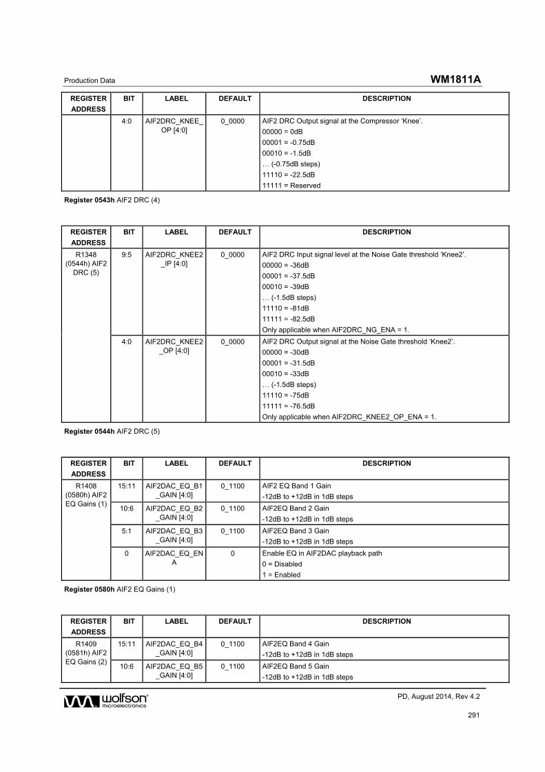
Production Data WM1811A
w PD, August 2014, Rev 4.2
291
REGISTER
ADDRESS
BIT LABEL DEFAULT DESCRIPTION
4:0 AIF2DRC_KNEE_OP [4:0]
0_0000 AIF2 DRC Output signal at the Compressor ‘Knee’.
00000 = 0dB
00001 = -0.75dB
00010 = -1.5dB
… (-0.75dB steps)
11110 = -22.5dB
11111 = Reserved
Register 0543h AIF2 DRC (4)
REGISTER
ADDRESS
BIT LABEL DEFAULT DESCRIPTION
R1348 (0544h) AIF2
DRC (5)
9:5 AIF2DRC_KNEE2_IP [4:0]
0_0000 AIF2 DRC Input signal level at the Noise Gate threshold ‘Knee2’.
00000 = -36dB
00001 = -37.5dB
00010 = -39dB
… (-1.5dB steps)
11110 = -81dB
11111 = -82.5dB
Only applicable when AIF2DRC_NG_ENA = 1.
4:0 AIF2DRC_KNEE2_OP [4:0]
0_0000 AIF2 DRC Output signal at the Noise Gate threshold ‘Knee2’.
00000 = -30dB
00001 = -31.5dB
00010 = -33dB
… (-1.5dB steps)
11110 = -75dB
11111 = -76.5dB
Only applicable when AIF2DRC_KNEE2_OP_ENA = 1.
Register 0544h AIF2 DRC (5)
REGISTER
ADDRESS
BIT LABEL DEFAULT DESCRIPTION
R1408 (0580h) AIF2 EQ Gains (1)
15:11 AIF2DAC_EQ_B1_GAIN [4:0]
0_1100 AIF2 EQ Band 1 Gain
-12dB to +12dB in 1dB steps
10:6 AIF2DAC_EQ_B2_GAIN [4:0]
0_1100 AIF2EQ Band 2 Gain
-12dB to +12dB in 1dB steps
5:1 AIF2DAC_EQ_B3_GAIN [4:0]
0_1100 AIF2EQ Band 3 Gain
-12dB to +12dB in 1dB steps
0 AIF2DAC_EQ_ENA
0 Enable EQ in AIF2DAC playback path
0 = Disabled
1 = Enabled
Register 0580h AIF2 EQ Gains (1)
REGISTER
ADDRESS
BIT LABEL DEFAULT DESCRIPTION
R1409 (0581h) AIF2 EQ Gains (2)
15:11 AIF2DAC_EQ_B4_GAIN [4:0]
0_1100 AIF2EQ Band 4 Gain
-12dB to +12dB in 1dB steps
10:6 AIF2DAC_EQ_B5_GAIN [4:0]
0_1100 AIF2EQ Band 5 Gain
-12dB to +12dB in 1dB steps
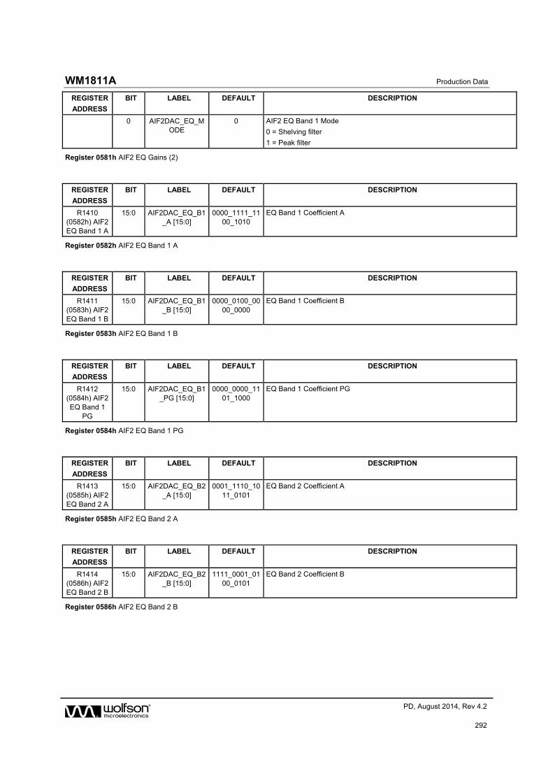
WM1811A Production Data
w PD, August 2014, Rev 4.2
292
REGISTER
ADDRESS
BIT LABEL DEFAULT DESCRIPTION
0 AIF2DAC_EQ_MODE
0 AIF2 EQ Band 1 Mode
0 = Shelving filter
1 = Peak filter
Register 0581h AIF2 EQ Gains (2)
REGISTER
ADDRESS
BIT LABEL DEFAULT DESCRIPTION
R1410 (0582h) AIF2 EQ Band 1 A
15:0 AIF2DAC_EQ_B1_A [15:0]
0000_1111_1100_1010
EQ Band 1 Coefficient A
Register 0582h AIF2 EQ Band 1 A
REGISTER
ADDRESS
BIT LABEL DEFAULT DESCRIPTION
R1411 (0583h) AIF2 EQ Band 1 B
15:0 AIF2DAC_EQ_B1_B [15:0]
0000_0100_0000_0000
EQ Band 1 Coefficient B
Register 0583h AIF2 EQ Band 1 B
REGISTER
ADDRESS
BIT LABEL DEFAULT DESCRIPTION
R1412 (0584h) AIF2 EQ Band 1
PG
15:0 AIF2DAC_EQ_B1_PG [15:0]
0000_0000_1101_1000
EQ Band 1 Coefficient PG
Register 0584h AIF2 EQ Band 1 PG
REGISTER
ADDRESS
BIT LABEL DEFAULT DESCRIPTION
R1413 (0585h) AIF2 EQ Band 2 A
15:0 AIF2DAC_EQ_B2_A [15:0]
0001_1110_1011_0101
EQ Band 2 Coefficient A
Register 0585h AIF2 EQ Band 2 A
REGISTER
ADDRESS
BIT LABEL DEFAULT DESCRIPTION
R1414 (0586h) AIF2 EQ Band 2 B
15:0 AIF2DAC_EQ_B2_B [15:0]
1111_0001_0100_0101
EQ Band 2 Coefficient B
Register 0586h AIF2 EQ Band 2 B

Production Data WM1811A
w PD, August 2014, Rev 4.2
293
REGISTER
ADDRESS
BIT LABEL DEFAULT DESCRIPTION
R1415 (0587h) AIF2 EQ Band 2 C
15:0 AIF2DAC_EQ_B2_C [15:0]
0000_1011_0111_0101
EQ Band 2 Coefficient C
Register 0587h AIF2 EQ Band 2 C
REGISTER
ADDRESS
BIT LABEL DEFAULT DESCRIPTION
R1416 (0588h) AIF2 EQ Band 2
PG
15:0 AIF2DAC_EQ_B2_PG [15:0]
0000_0001_1100_0101
EQ Band 2 Coefficient PG
Register 0588h AIF2 EQ Band 2 PG
REGISTER
ADDRESS
BIT LABEL DEFAULT DESCRIPTION
R1417 (0589h) AIF2 EQ Band 3 A
15:0 AIF2DAC_EQ_B3_A [15:0]
0001_1100_0101_1000
EQ Band 3 Coefficient A
Register 0589h AIF2 EQ Band 3 A
REGISTER
ADDRESS
BIT LABEL DEFAULT DESCRIPTION
R1418 (058Ah) AIF2 EQ Band 3 B
15:0 AIF2DAC_EQ_B3_B [15:0]
1111_0011_0111_0011
EQ Band 3 Coefficient B
Register 058Ah AIF2 EQ Band 3 B
REGISTER
ADDRESS
BIT LABEL DEFAULT DESCRIPTION
R1419 (058Bh) AIF2 EQ Band 3 C
15:0 AIF2DAC_EQ_B3_C [15:0]
0000_1010_0101_0100
EQ Band 3 Coefficient C
Register 058Bh AIF2 EQ Band 3 C
REGISTER
ADDRESS
BIT LABEL DEFAULT DESCRIPTION
R1420 (058Ch) AIF2 EQ Band 3
PG
15:0 AIF2DAC_EQ_B3_PG [15:0]
0000_0101_0101_1000
EQ Band 3 Coefficient PG
Register 058Ch AIF2 EQ Band 3 PG

WM1811A Production Data
w PD, August 2014, Rev 4.2
294
REGISTER
ADDRESS
BIT LABEL DEFAULT DESCRIPTION
R1421 (058Dh) AIF2 EQ Band 4 A
15:0 AIF2DAC_EQ_B4_A [15:0]
0001_0110_1000_1110
EQ Band 4 Coefficient A
Register 058Dh AIF2 EQ Band 4 A
REGISTER
ADDRESS
BIT LABEL DEFAULT DESCRIPTION
R1422 (058Eh) AIF2 EQ Band 4 B
15:0 AIF2DAC_EQ_B4_B [15:0]
1111_1000_0010_1001
EQ Band 4 Coefficient B
Register 058Eh AIF2 EQ Band 4 B
REGISTER
ADDRESS
BIT LABEL DEFAULT DESCRIPTION
R1423 (058Fh) AIF2 EQ Band 4 C
15:0 AIF2DAC_EQ_B4_C [15:0]
0000_0111_1010_1101
EQ Band 4 Coefficient C
Register 058Fh AIF2 EQ Band 4 C
REGISTER
ADDRESS
BIT LABEL DEFAULT DESCRIPTION
R1424 (0590h) AIF2 EQ Band 4
PG
15:0 AIF2DAC_EQ_B4_PG [15:0]
0001_0001_0000_0011
EQ Band 4 Coefficient PG
Register 0590h AIF2 EQ Band 4 PG
REGISTER
ADDRESS
BIT LABEL DEFAULT DESCRIPTION
R1425 (0591h) AIF2 EQ Band 5 A
15:0 AIF2DAC_EQ_B5_A [15:0]
0000_0101_0110_0100
EQ Band 5 Coefficient A
Register 0591h AIF2 EQ Band 5 A
REGISTER
ADDRESS
BIT LABEL DEFAULT DESCRIPTION
R1426 (0592h) AIF2 EQ Band 5 B
15:0 AIF2DAC_EQ_B5_B [15:0]
0000_0101_0101_1001
EQ Band 5 Coefficient B
Register 0592h AIF2 EQ Band 5 B

Production Data WM1811A
w PD, August 2014, Rev 4.2
295
REGISTER
ADDRESS
BIT LABEL DEFAULT DESCRIPTION
R1427 (0593h) AIF2 EQ Band 5
PG
15:0 AIF2DAC_EQ_B5_PG [15:0]
0100_0000_0000_0000
EQ Band 5 Coefficient PG
Register 0593h AIF2 EQ Band 5 PG
REGISTER
ADDRESS
BIT LABEL DEFAULT DESCRIPTION
R1428 (0594h) AIF2 EQ Band 1 C
15:0 AIF2DAC_EQ_B1_C [15:0]
0000_0000_0000_0000
EQ Band 1 Coefficient C
Register 0594h AIF2 EQ Band 1 C
REGISTER
ADDRESS
BIT LABEL DEFAULT DESCRIPTION
R1536 (0600h)
DAC1 Mixer Volumes
8:5 ADCR_DAC1_VOL [3:0]
0000 Sidetone STR to DAC1L and DAC1R Volume
0000 = -36dB
0001 = -33dB
…. (3dB steps)
1011 = -3dB
1100 = 0dB
3:0 ADCL_DAC1_VOL [3:0]
0000 Sidetone STL to DAC1L and DAC1R Volume
0000 = -36dB
0001 = -33dB
…. (3dB steps)
1011 = -3dB
1100 = 0dB
Register 0600h DAC1 Mixer Volumes
REGISTER
ADDRESS
BIT LABEL DEFAULT DESCRIPTION
R1537 (0601h)
DAC1 Left Mixer Routing
5 ADCR_TO_DAC1L
0 Enable Sidetone STR to DAC1L
0 = Disabled
1 = Enabled
4 ADCL_TO_DAC1L
0 Enable Sidetone STL to DAC1L
0 = Disabled
1 = Enabled
2 AIF2DACL_TO_DAC1L
0 Enable AIF2 (Left) to DAC1L
0 = Disabled
1 = Enabled
0 AIF1DAC1L_TO_DAC1L
0 Enable AIF1 (Left) to DAC1L
0 = Disabled
1 = Enabled
Register 0601h DAC1 Left Mixer Routing

WM1811A Production Data
w PD, August 2014, Rev 4.2
296
REGISTER
ADDRESS
BIT LABEL DEFAULT DESCRIPTION
R1538 (0602h)
DAC1 Right Mixer Routing
5 ADCR_TO_DAC1R
0 Enable Sidetone STR to DAC1R
0 = Disabled
1 = Enabled
4 ADCL_TO_DAC1R
0 Enable Sidetone STL to DAC1R
0 = Disabled
1 = Enabled
2 AIF2DACR_TO_DAC1R
0 Enable AIF2 (Right) to DAC1R
0 = Disabled
1 = Enabled
0 AIF1DAC1R_TO_DAC1R
0 Enable AIF1 (Right) to DAC1R
0 = Disabled
1 = Enabled
Register 0602h DAC1 Right Mixer Routing
REGISTER
ADDRESS
BIT LABEL DEFAULT DESCRIPTION
R1539 (0603h)
AIF2ADC Mixer
Volumes
8:5 ADCR_AIF2ADC_VOL [3:0]
0000 Sidetone STR to AIF2 Tx Volume
0000 = -36dB
0001 = -33dB
…. (3dB steps)
1011 = -3dB
1100 = 0dB
3:0 ADCL_AIF2ADC_VOL [3:0]
0000 Sidetone STL to AIF2 Tx Volume
0000 = -36dB
0001 = -33dB
…. (3dB steps)
1011 = -3dB
1100 = 0dB
Register 0603h AIF2ADC Mixer Volumes
REGISTER
ADDRESS
BIT LABEL DEFAULT DESCRIPTION
R1540 (0604h)
AIF2ADC Left Mixer Routing
5 ADCR_TO_AIF2ADCL
0 Enable Sidetone STR to AIF2 Tx (Left)
0 = Disabled
1 = Enabled
4 ADCL_TO_AIF2ADCL
0 Enable Sidetone STL to AIF2 Tx (Left)
0 = Disabled
1 = Enabled
2 AIF2DACL_TO_AIF2ADCL
0 Enable AIF2 (Left) to AIF2 Tx (Left)
0 = Disabled
1 = Enabled
0 AIF1DAC1L_TO_AIF2ADCL
0 Enable AIF1 (Left) to AIF2 Tx (Left)
0 = Disabled
1 = Enabled
Register 0604h AIF2ADC Left Mixer Routing

Production Data WM1811A
w PD, August 2014, Rev 4.2
297
REGISTER
ADDRESS
BIT LABEL DEFAULT DESCRIPTION
R1541 (0605h)
AIF2ADC Right Mixer
Routing
5 ADCR_TO_AIF2ADCR
0 Enable Sidetone STR to AIF2 Tx (Right)
0 = Disabled
1 = Enabled
4 ADCL_TO_AIF2ADCR
0 Enable Sidetone STL to AIF2 Tx (Right)
0 = Disabled
1 = Enabled
2 AIF2DACR_TO_AIF2ADCR
0 Enable AIF2 (Right) to AIF2 Tx (Right)
0 = Disabled
1 = Enabled
0 AIF1DAC1R_TO_AIF2ADCR
0 Enable AIF1 (Right) to AIF2 Tx (Right)
0 = Disabled
1 = Enabled
Register 0605h AIF2ADC Right Mixer Routing
REGISTER
ADDRESS
BIT LABEL DEFAULT DESCRIPTION
R1542 (0606h) AIF1
ADC1 Left Mixer Routing
1 ADC1L_TO_AIF1ADC1L
0 Enable ADCL / DMIC (Left) to AIF1 (Left) output
0 = Disabled
1 = Enabled
0 AIF2DACL_TO_AIF1ADC1L
0 Enable AIF2 (Left) to AIF1 (Left) output
0 = Disabled
1 = Enabled
Register 0606h AIF1 ADC1 Left Mixer Routing
REGISTER
ADDRESS
BIT LABEL DEFAULT DESCRIPTION
R1543 (0607h) AIF1 ADC1 Right
Mixer Routing
1 ADC1R_TO_AIF1ADC1R
0 Enable ADCR / DMIC (Right) to AIF1 (Right) output
0 = Disabled
1 = Enabled
0 AIF2DACR_TO_AIF1ADC1R
0 Enable AIF2 (Right) to AIF1 (Right) output
0 = Disabled
1 = Enabled
Register 0607h AIF1 ADC1 Right Mixer Routing
REGISTER
ADDRESS
BIT LABEL DEFAULT DESCRIPTION
R1552 (0610h)
DAC1 Left Volume
9 DAC1L_MUTE 1 DAC1L Soft Mute Control
0 = DAC Un-mute
1 = DAC Mute
8 DAC1_VU 0 DAC1L and DAC1R Volume Update
Writing a 1 to this bit will cause the DAC1L and DAC1R volume to be updated simultaneously

WM1811A Production Data
w PD, August 2014, Rev 4.2
298
REGISTER
ADDRESS
BIT LABEL DEFAULT DESCRIPTION
7:0 DAC1L_VOL [7:0] 1100_0000 DAC1L Digital Volume 00h = MUTE 01h = -71.625dB … (0.375dB steps) C0h = 0dB … (0.375dB steps) E0h = 12dB FFh = 12dB
Register 0610h DAC1 Left Volume
REGISTER
ADDRESS
BIT LABEL DEFAULT DESCRIPTION
R1553 (0611h)
DAC1 Right Volume
9 DAC1R_MUTE 1 DAC1R Soft Mute Control
0 = DAC Un-mute
1 = DAC Mute
8 DAC1_VU 0 DAC1L and DAC1R Volume Update
Writing a 1 to this bit will cause the DAC1L and DAC1R volume to be updated simultaneously
7:0 DAC1R_VOL [7:0] 1100_0000 DAC1R Digital Volume 00h = MUTE 01h = -71.625dB … (0.375dB steps) C0h = 0dB … (0.375dB steps) E0h = 12dB FFh = 12dB
Register 0611h DAC1 Right Volume
REGISTER
ADDRESS
BIT LABEL DEFAULT DESCRIPTION
R1554 (0612h)
AIF2TX Left Volume
9 AIF2TXL_MUTE 1 AIF2 Tx (Left) Soft Mute Control
0 = Un-mute
1 = Mute
8 AIF2TX_VU 0 AIF2 Tx (Left) and AIF2 Tx (Right) Volume Update
Writing a 1 to this bit will cause the AIF2TXL and AIF2TXR volume to be updated simultaneously
7:0 AIF2TXL_VOL [7:0]
1100_0000 AIF2 Tx (Left) Volume Digital Volume 00h = MUTE 01h = -71.625dB … (0.375dB steps) C0h = 0dB … (0.375dB steps) E0h = 12dB FFh = 12dB
Register 0612h AIF2TX Left Volume

Production Data WM1811A
w PD, August 2014, Rev 4.2
299
REGISTER
ADDRESS
BIT LABEL DEFAULT DESCRIPTION
R1555 (0613h)
AIF2TX Right Volume
9 AIF2TXR_MUTE 1 AIF2 Tx (Right) Soft Mute Control
0 = DAC Un-mute
1 = DAC Mute
8 AIF2TX_VU 0 AIF2 Tx (Left) and AIF2 Tx (Right) Volume Update
Writing a 1 to this bit will cause the AIF2TXL and AIF2TXR volume to be updated simultaneously
7:0 AIF2TXR_VOL [7:0]
1100_0000 AIF2 Tx (Right) Digital Volume
00h = MUTE
01h = -71.625dB
… (0.375dB steps)
C0h = 0dB
… (0.375dB steps)
E0h = 12dB
FFh = 12dB
Register 0613h AIF2TX Right Volume
REGISTER
ADDRESS
BIT LABEL DEFAULT DESCRIPTION
R1556 (0614h) DAC
Softmute
1 DAC_SOFTMUTEMODE
0 DAC/AIF2 Digital Output Mixer Unmute Ramp select
0 = Unmuting the DAC / AIF2 volume will immediately apply the DAC1[L/R]_VOL or AIF2TX[L/R]_VOL settings.
1 = Unmuting the DAC / AIF2 volume will cause a gradual ramp up to the DAC1[L/R]_VOL or AIF2TX[L/R]_VOL settings.
0 DAC_MUTERATE 0 DAC/AIF2 Digital Output Mixer Soft Mute Ramp Rate
0 = Fast ramp (fs/2, maximum ramp time is 10.7ms at fs=48k)
1 = Slow ramp (fs/32, maximum ramp time is 171ms at fs=48k)
(Note: ramp rate scales with sample rate.)
Register 0614h DAC Softmute
REGISTER
ADDRESS
BIT LABEL DEFAULT DESCRIPTION
R1568 (0620h)
Oversampling
1 ADC_OSR128 1 ADC / Digital Microphone Oversample Rate Select
0 = Low Power
1 = High Performance
0 DAC_OSR128 0 DAC Oversample Rate Select
0 = Low Power
1 = High Performance
Register 0620h Oversampling

WM1811A Production Data
w PD, August 2014, Rev 4.2
300
REGISTER
ADDRESS
BIT LABEL DEFAULT DESCRIPTION
R1569 (0621h) Sidetone
9:7 ST_HPF_CUT [2:0]
000 Sidetone HPF cut-off frequency (relative to 44.1kHz sample rate)
000 = 2.7kHz
001 = 1.35kHz
010 = 675Hz
011 = 370Hz
100 = 180Hz
101 = 90Hz
110 = 45Hz
111 = Reserved
Note - the cut-off frequencies scale with the Digital Mixing (SYSCLK) clocking rate. The quoted figures apply to 44.1kHz sample rate.
6 ST_HPF 0 Digital Sidetone HPF Select
0 = Disabled
1 = Enabled
Register 0621h Sidetone
REGISTER
ADDRESS
BIT LABEL DEFAULT DESCRIPTION
R1792 (0700h) GPIO 1
15 GP1_DIR 1 GPIO1 Pin Direction
0 = Output
1 = Input
14 GP1_PU 0 GPIO1 Pull-Up Enable
0 = Disabled
1 = Enabled
13 GP1_PD 0 GPIO1 Pull-Down Enable
0 = Disabled
1 = Enabled
10 GP1_POL 0 GPIO1 Polarity Select
0 = Non-inverted (Active High)
1 = Inverted (Active Low)
9 GP1_OP_CFG 0 GPIO1 Output Configuration
0 = CMOS
1 = Open Drain
8 GP1_DB 1 GPIO1 Input De-bounce
0 = Disabled
1 = Enabled
6 GP1_LVL 0 GPIO1 level. Write to this bit to set a GPIO output. Read from this bit to read GPIO input level.
For output functions only, when GP1_POL is set, the register contains the opposite logic level to the external pin.
4:0 GP1_FN [4:0] 0_0000 GPIO1 Pin Function
00h = ADCLRCLK1
01h = GPIO
02h = Reserved
03h = IRQ
04h = Temperature (Shutdown) status
05h = MICDET status
06h = Reserved
07h = Reserved
08h = Reserved
09h = FLL1 Lock

Production Data WM1811A
w PD, August 2014, Rev 4.2
301
REGISTER
ADDRESS
BIT LABEL DEFAULT DESCRIPTION
0Ah = FLL2 Lock
0Bh = SRC1 Lock
0Ch = SRC2 Lock
0Dh = AIF1 DRC Signal Detect
0Eh = Reserved
0Fh = AIF2 DRC Signal Detect
10h = Reserved
11h = FIFO Error
12h = OPCLK Clock output
13h = Temperature (Warning) status
14h = DC Servo Done
15h = FLL1 Clock output
16h = FLL2 Clock output
17h to 1Fh = Reserved
Register 0700h GPIO 1
REGISTER
ADDRESS
BIT LABEL DEFAULT DESCRIPTION
R1793 (0701h) Pull
Control (MCLK2)
15 Reserved 1 Reserved - do not change
14 MCLK2_PU 0 MCLK2 Pull-up enable
0 = Disabled
1 = Enabled
13 MCLK2_PD 1 MCLK2 Pull-down enable
0 = Disabled
1 = Enabled
8 Reserved 1 Reserved - do not change
0 Reserved 1 Reserved - do not change
Register 0701h Pull Control (MCLK2)
REGISTER
ADDRESS
BIT LABEL DEFAULT DESCRIPTION
R1794 (0702h) Pull
Control (BCLK2)
15 Reserved 1 Reserved - do not change
14 BCLK2_PU 0 BCLK2 Pull-up enable
0 = Disabled
1 = Enabled
13 BCLK2_PD 1 BCLK2 Pull-down enable
0 = Disabled
1 = Enabled
8 Reserved 1 Reserved - do not change
0 Reserved 1 Reserved - do not change
Register 0702h Pull Control (BCLK2)

WM1811A Production Data
w PD, August 2014, Rev 4.2
302
REGISTER
ADDRESS
BIT LABEL DEFAULT DESCRIPTION
R1795 (0703h) Pull
Control (DACLRCLK
2)
15 Reserved 1 Reserved - do not change
14 DACLRCLK2_PU 0 DACLRCLK2 Pull-up enable
0 = Disabled
1 = Enabled
13 DACLRCLK2_PD 1 DACLRCLK2 Pull-down enable
0 = Disabled
1 = Enabled
8 Reserved 1 Reserved - do not change
0 Reserved 1 Reserved - do not change
Register 0703h Pull Control (DACLRCLK2)
REGISTER
ADDRESS
BIT LABEL DEFAULT DESCRIPTION
R1796 (0704h) Pull
Control (DACDAT2)
15 Reserved 1 Reserved - do not change
14 DACDAT2_PU 0 DACDAT2 Pull-up enable
0 = Disabled
1 = Enabled
13 DACDAT2_PD 1 DACDAT2 Pull-down enable
0 = Disabled
1 = Enabled
8 Reserved 1 Reserved - do not change
0 Reserved 1 Reserved - do not change
Register 0704h Pull Control (DACDAT2)
REGISTER
ADDRESS
BIT LABEL DEFAULT DESCRIPTION
R1797 (0705h)
JACKDET Ctrl
15 1 Reserved - do not change
13 1 Reserved - do not change
8 JACKDET_DB 1 JACKDET input de-bounce
0 = Disabled
1 = Enabled
6 JACKDET_LVL 0 JACKDET input status
0 = Jack not detected
1 = Jack is detected
0 1 Reserved - do not change
Register 0705hJACKDET Ctrl
REGISTER
ADDRESS
BIT LABEL DEFAULT DESCRIPTION
R1799 (0707h) GPIO 8
15 GP8_DIR 1 GPIO8 Pin Direction
0 = Output
1 = Input
14 GP8_PU 0 GPIO8 Pull-Up Enable
0 = Disabled
1 = Enabled

Production Data WM1811A
w PD, August 2014, Rev 4.2
303
REGISTER
ADDRESS
BIT LABEL DEFAULT DESCRIPTION
13 GP8_PD 1 GPIO8 Pull-Down Enable
0 = Disabled
1 = Enabled
10 GP8_POL 0 GPIO8 Polarity Select
0 = Non-inverted (Active High)
1 = Inverted (Active Low)
9 GP8_OP_CFG 0 GPIO8 Output Configuration
0 = CMOS
1 = Open Drain
8 GP8_DB 1 GPIO8 Input De-bounce
0 = Disabled
1 = Enabled
6 GP8_LVL 0 GPIO8 level. Write to this bit to set a GPIO output. Read from this bit to read GPIO input level.
For output functions only, when GP8_POL is set, the register contains the opposite logic level to the external pin.
4:0 GP8_FN [4:0] 0_0001 GPIO8 Pin Function
00h = DACDAT3
01h = GPIO
02h = Reserved
03h = IRQ
04h = Temperature (Shutdown) status
05h = MICDET status
06h = Reserved
07h = Reserved
08h = Reserved
09h = FLL1 Lock
0Ah = FLL2 Lock
0Bh = SRC1 Lock
0Ch = SRC2 Lock
0Dh = AIF1 DRC Signal Detect
0Eh = Reserved
0Fh = AIF2 DRC Signal Detect
10h = Reserved
11h = FIFO Error
12h = OPCLK Clock output
13h = Temperature (Warning) status
14h = DC Servo Done
15h = FLL1 Clock output
16h = FLL2 Clock output
17h to 1Fh = Reserved
Register 0707h GPIO 8

WM1811A Production Data
w PD, August 2014, Rev 4.2
304
REGISTER
ADDRESS
BIT LABEL DEFAULT DESCRIPTION
R1800 (0708h) GPIO 9
15 GP9_DIR 1 GPIO9 Pin Direction
0 = Output
1 = Input
14 GP9_PU 0 GPIO9 Pull-Up Enable
0 = Disabled
1 = Enabled
13 GP9_PD 1 GPIO9 Pull-Down Enable
0 = Disabled
1 = Enabled
10 GP9_POL 0 GPIO9 Polarity Select
0 = Non-inverted (Active High)
1 = Inverted (Active Low)
9 GP9_OP_CFG 0 GPIO9 Output Configuration
0 = CMOS
1 = Open Drain
8 GP9_DB 1 GPIO9 Input De-bounce
0 = Disabled
1 = Enabled
6 GP9_LVL 0 GPIO9 level. Write to this bit to set a GPIO output. Read from this bit to read GPIO input level.
For output functions only, when GP9_POL is set, the register contains the opposite logic level to the external pin.
4:0 GP9_FN [4:0] 0_0001 GPIO9 Pin Function
00h = ADCDAT3
01h = GPIO
02h = Reserved
03h = IRQ
04h = Temperature (Shutdown) status
05h = MICDET status
06h = Reserved
07h = Reserved
08h = Reserved
09h = FLL1 Lock
0Ah = FLL2 Lock
0Bh = SRC1 Lock
0Ch = SRC2 Lock
0Dh = AIF1 DRC Signal Detect
0Eh = Reserved
0Fh = AIF2 DRC Signal Detect
10h = Reserved
11h = FIFO Error
12h = OPCLK Clock output
13h = Temperature (Warning) status
14h = DC Servo Done
15h = FLL1 Clock output
16h = FLL2 Clock output
17h to 1Fh = Reserved
Register 0708h GPIO 9

Production Data WM1811A
w PD, August 2014, Rev 4.2
305
REGISTER
ADDRESS
BIT LABEL DEFAULT DESCRIPTION
R1801 (0709h) GPIO 10
15 GP10_DIR 1 GPIO10 Pin Direction
0 = Output
1 = Input
14 GP10_PU 0 GPIO10 Pull-Up Enable
0 = Disabled
1 = Enabled
13 GP10_PD 1 GPIO10 Pull-Down Enable
0 = Disabled
1 = Enabled
10 GP10_POL 0 GPIO10 Polarity Select
0 = Non-inverted (Active High)
1 = Inverted (Active Low)
9 GP10_OP_CFG 0 GPIO10 Output Configuration
0 = CMOS
1 = Open Drain
8 GP10_DB 1 GPIO10 Input De-bounce
0 = Disabled
1 = Enabled
6 GP10_LVL 0 GPIO10 level. Write to this bit to set a GPIO output. Read from this bit to read GPIO input level.
For output functions only, when GP10_POL is set, the register contains the opposite logic level to the external pin.
4:0 GP10_FN [4:0] 0_0001 GPIO10 Pin Function
00h = LRCLK3
01h = GPIO
02h = Reserved
03h = IRQ
04h = Temperature (Shutdown) status
05h = MICDET status
06h = Reserved
07h = Reserved
08h = Reserved
09h = FLL1 Lock
0Ah = FLL2 Lock
0Bh = SRC1 Lock
0Ch = SRC2 Lock
0Dh = AIF1 DRC Signal Detect
0Eh = Reserved
0Fh = AIF2 DRC Signal Detect
10h = Reserved
11h = FIFO Error
12h = OPCLK Clock output
13h = Temperature (Warning) status
14h = DC Servo Done
15h = FLL1 Clock output
16h = FLL2 Clock output
17h to 1Fh = Reserved
Register 0709h GPIO 10
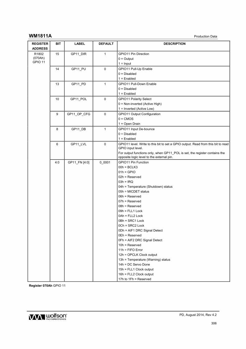
WM1811A Production Data
w PD, August 2014, Rev 4.2
306
REGISTER
ADDRESS
BIT LABEL DEFAULT DESCRIPTION
R1802 (070Ah) GPIO 11
15 GP11_DIR 1 GPIO11 Pin Direction
0 = Output
1 = Input
14 GP11_PU 0 GPIO11 Pull-Up Enable
0 = Disabled
1 = Enabled
13 GP11_PD 1 GPIO11 Pull-Down Enable
0 = Disabled
1 = Enabled
10 GP11_POL 0 GPIO11 Polarity Select
0 = Non-inverted (Active High)
1 = Inverted (Active Low)
9 GP11_OP_CFG 0 GPIO11 Output Configuration
0 = CMOS
1 = Open Drain
8 GP11_DB 1 GPIO11 Input De-bounce
0 = Disabled
1 = Enabled
6 GP11_LVL 0 GPIO11 level. Write to this bit to set a GPIO output. Read from this bit to read GPIO input level.
For output functions only, when GP11_POL is set, the register contains the opposite logic level to the external pin.
4:0 GP11_FN [4:0] 0_0001 GPIO11 Pin Function
00h = BCLK3
01h = GPIO
02h = Reserved
03h = IRQ
04h = Temperature (Shutdown) status
05h = MICDET status
06h = Reserved
07h = Reserved
08h = Reserved
09h = FLL1 Lock
0Ah = FLL2 Lock
0Bh = SRC1 Lock
0Ch = SRC2 Lock
0Dh = AIF1 DRC Signal Detect
0Eh = Reserved
0Fh = AIF2 DRC Signal Detect
10h = Reserved
11h = FIFO Error
12h = OPCLK Clock output
13h = Temperature (Warning) status
14h = DC Servo Done
15h = FLL1 Clock output
16h = FLL2 Clock output
17h to 1Fh = Reserved
Register 070Ah GPIO 11

Production Data WM1811A
w PD, August 2014, Rev 4.2
307
REGISTER
ADDRESS
BIT LABEL DEFAULT DESCRIPTION
R1824 (0720h) Pull Control (1)
9 DMICDAT1_PU 0 DMICDAT Pull-Up enable
0 = Disabled
1 = Enabled
8 DMICDAT1_PD 0 DMICDAT Pull-Down enable
0 = Disabled
1 = Enabled
7 MCLK1_PU 0 MCLK1 Pull-up enable
0 = Disabled
1 = Enabled
6 MCLK1_PD 0 MCLK1 Pull-down enable
0 = Disabled
1 = Enabled
5 DACDAT1_PU 0 DACDAT1 Pull-up enable
0 = Disabled
1 = Enabled
4 DACDAT1_PD 0 DACDAT1 Pull-down enable
0 = Disabled
1 = Enabled
3 DACLRCLK1_PU 0 LRCLK1 Pull-up enable
0 = Disabled
1 = Enabled
2 DACLRCLK1_PD 0 LRCLK1 Pull-down enable
0 = Disabled
1 = Enabled
1 BCLK1_PU 0 BCLK1 Pull-up enable
0 = Disabled
1 = Enabled
0 BCLK1_PD 0 BCLK1 Pull-down enable
0 = Disabled
1 = Enabled
Register 0720h Pull Control (1)
REGISTER
ADDRESS
BIT LABEL DEFAULT DESCRIPTION
R1825 (0721h) Pull Control (2)
8 ADDR_PD 1 ADDR Pull-down enable
0 = Disabled
1 = Enabled
6 LDO2ENA_PD 1 LDO2ENA Pull-down enable
0 = Disabled
1 = Enabled
4 LDO1ENA_PD 1 LDO1ENA Pull-down enable
0 = Disabled
1 = Enabled
2 Reserved 1 Reserved - do not change
1 SPKMODE_PU 1 SPKMODE Pull-up enable
0 = Disabled
1 = Enabled
Register 0721h Pull Control (2)

WM1811A Production Data
w PD, August 2014, Rev 4.2
308
REGISTER
ADDRESS
BIT LABEL DEFAULT DESCRIPTION
R1840 (0730h) Interrupt Status 1
10 GP11_EINT 0 GPIO11 Interrupt
(Rising and falling edge triggered)
Note: Cleared when a ‘1’ is written.
9 GP10_EINT 0 GPIO10 Interrupt
(Rising and falling edge triggered)
Note: Cleared when a ‘1’ is written.
8 GP9_EINT 0 GPIO9 Interrupt
(Rising and falling edge triggered)
Note: Cleared when a ‘1’ is written.
7 GP8_EINT 0 GPIO8 Interrupt
(Rising and falling edge triggered)
Note: Cleared when a ‘1’ is written.
5 JACKDET_EINT 0 Jack Detect Interrupt
(Rising and falling edge triggered)
Note: Cleared when a ‘1’ is written.
0 GP1_EINT 0 GPIO1 Interrupt
(Rising and falling edge triggered)
Note: Cleared when a ‘1’ is written.
Register 0730h Interrupt Status 1
REGISTER
ADDRESS
BIT LABEL DEFAULT DESCRIPTION
R1841 (0731h) Interrupt Status 2
15 TEMP_WARN_EINT
0 Temperature Warning Interrupt
(Rising and falling edge triggered)
Note: Cleared when a ‘1’ is written.
14 DCS_DONE_EINT
0 DC Servo Interrupt
(Rising edge triggered)
Note: Cleared when a ‘1’ is written.
12 FIFOS_ERR_EINT
0 Digital Core FIFO Error Interrupt
(Rising edge triggered)
Note: Cleared when a ‘1’ is written.
11 AIF2DRC_SIG_DET_EINT
0 AIF2 DRC Activity Detect Interrupt
(Rising edge triggered)
Note: Cleared when a ‘1’ is written.
9 AIF1DRC1_SIG_DET_EINT
0 AIF1 DRC Activity Detect Interrupt
(Rising edge triggered)
Note: Cleared when a ‘1’ is written.
8 SRC2_LOCK_EINT
0 SRC2 Lock Interrupt
(Rising and falling edge triggered)
Note: Cleared when a ‘1’ is written.
7 SRC1_LOCK_EINT
0 SRC1 Lock Interrupt
(Rising and falling edge triggered)
Note: Cleared when a ‘1’ is written.
6 FLL2_LOCK_EINT
0 FLL2 Lock Interrupt
(Rising and falling edge triggered)
Note: Cleared when a ‘1’ is written.
5 FLL1_LOCK_EINT
0 FLL1 Lock Interrupt
(Rising and falling edge triggered)
Note: Cleared when a ‘1’ is written.

Production Data WM1811A
w PD, August 2014, Rev 4.2
309
REGISTER
ADDRESS
BIT LABEL DEFAULT DESCRIPTION
1 MICD_EINT 0 Microphone Detection Interrupt
(Rising and falling edge triggered)
Note: Cleared when a ‘1’ is written.
0 TEMP_SHUT_EINT
0 Temperature Shutdown Interrupt
(Rising and falling edge triggered)
Note: Cleared when a ‘1’ is written.
Register 0731h Interrupt Status 2
REGISTER
ADDRESS
BIT LABEL DEFAULT DESCRIPTION
R1842 (0732h)
Interrupt Raw Status 2
15 TEMP_WARN_STS
0 Temperature Warning status
0 = Temperature is below warning level
1 = Temperature is above warning level
14 DCS_DONE_STS 0 DC Servo status
0 = DC Servo not complete
1 = DC Servo complete
12 FIFOS_ERR_STS 0 Digital Core FIFO Error status
0 = Normal operation
1 = FIFO Error
11 AIF2DRC_SIG_DET_STS
0 AIF2 DRC Signal Detect status
0 = Signal threshold not exceeded
1 = Signal threshold not exceeded
9 AIF1DRC1_SIG_DET_STS
0 AIF1 DRC Signal Detect status
0 = Signal threshold not exceeded
1 = Signal threshold not exceeded
8 SRC2_LOCK_STS
0 SRC2 Lock status
0 = Not locked
1 = Locked
7 SRC1_LOCK_STS
0 SRC1 Lock status
0 = Not locked
1 = Locked
6 FLL2_LOCK_STS 0 FLL2 Lock status
0 = Not locked
1 = Locked
5 FLL1_LOCK_STS 0 FLL1 Lock status
0 = Not locked
1 = Locked
0 TEMP_SHUT_STS
0 Temperature Shutdown status
0 = Temperature is below shutdown level
1 = Temperature is above shutdown level
Register 0732h Interrupt Raw Status 2
REGISTER
ADDRESS
BIT LABEL DEFAULT DESCRIPTION
R1848 (0738h) Interrupt Status 1
Mask
10 IM_GP11_EINT 1 GPIO11 Interrupt mask.
0 = Do not mask interrupt.
1 = Mask interrupt.
9 IM_GP10_EINT 1 GPIO10Interrupt mask.
0 = Do not mask interrupt.

WM1811A Production Data
w PD, August 2014, Rev 4.2
310
REGISTER
ADDRESS
BIT LABEL DEFAULT DESCRIPTION
1 = Mask interrupt.
8 IM_GP9_EINT 1 GPIO9Interrupt mask.
0 = Do not mask interrupt.
1 = Mask interrupt.
7 IM_GP8_EINT 1 GPIO8Interrupt mask.
0 = Do not mask interrupt.
1 = Mask interrupt.
6 Reserved 1 Reserved - do not change
5 IM_JACKDET_EINT
1 Jack DetectInterrupt mask.
0 = Do not mask interrupt.
1 = Mask interrupt.
4 Reserved 1 Reserved - do not change
3 Reserved 1 Reserved - do not change
2 Reserved 1 Reserved - do not change
1 Reserved 1 Reserved - do not change
0 IM_GP1_EINT 1 GPIO1Interrupt mask.
0 = Do not mask interrupt.
1 = Mask interrupt.
Register 0738h Interrupt Status 1 Mask
REGISTER
ADDRESS
BIT LABEL DEFAULT DESCRIPTION
R1849 (0739h) Interrupt Status 2
Mask
15 IM_TEMP_WARN_EINT
1 Temperature Warning Interrupt mask.
0 = Do not mask interrupt.
1 = Mask interrupt.
14 IM_DCS_DONE_EINT
1 DC Servo Interrupt mask.
0 = Do not mask interrupt.
1 = Mask interrupt.
12 IM_FIFOS_ERR_EINT
1 Digital Core FIFO Error Interrupt mask.
0 = Do not mask interrupt.
1 = Mask interrupt.
11 IM_AIF2DRC_SIG_DET_EINT
1 AIF2 DRC Activity Detect Interrupt mask.
0 = Do not mask interrupt.
1 = Mask interrupt.
9 IM_AIF1DRC1_SIG_DET_EINT
1 AIF1 DRC Activity Detect Interrupt mask.
0 = Do not mask interrupt.
1 = Mask interrupt.
8 IM_SRC2_LOCK_EINT
1 SRC2 Lock Interrupt mask.
0 = Do not mask interrupt.
1 = Mask interrupt.
7 IM_SRC1_LOCK_EINT
1 SRC1 Lock Interrupt mask.
0 = Do not mask interrupt.
1 = Mask interrupt.
6 IM_FLL2_LOCK_EINT
1 FLL2 Lock Interrupt mask.
0 = Do not mask interrupt.
1 = Mask interrupt.
5 IM_FLL1_LOCK_EINT
1 FLL1 Lock Interrupt mask.
0 = Do not mask interrupt.
1 = Mask interrupt.

Production Data WM1811A
w PD, August 2014, Rev 4.2
311
REGISTER
ADDRESS
BIT LABEL DEFAULT DESCRIPTION
1 IM_MICD_EINT 1 Microphone Detection Interrupt mask.
0 = Do not mask interrupt.
1 = Mask interrupt.
0 IM_TEMP_SHUT_EINT
1 Temperature Shutdown Interrupt mask.
0 = Do not mask interrupt.
1 = Mask interrupt.
Register 0739h Interrupt Status 2 Mask
REGISTER
ADDRESS
BIT LABEL DEFAULT DESCRIPTION
R1856 (0740h) Interrupt Control
0 IM_IRQ 0 IRQ Output Interrupt mask.
0 = Do not mask interrupt.
1 = Mask interrupt.
Register 0740h Interrupt Control
REGISTER
ADDRESS
BIT LABEL DEFAULT DESCRIPTION
R1864 (0748h) IRQ Debounce
5 TEMP_WARN_DB
1 Thermal Warning de-bounce
0 = Disabled
1 = Enabled
4 Reserved 1 Reserved - do not change
3 Reserved 1 Reserved - do not change
2 Reserved 1 Reserved - do not change
1 Reserved 1 Reserved - do not change
0 TEMP_SHUT_DB 1 Thermal shutdown de-bounce
0 = Disabled
1 = Enabled
Register 0748h IRQ Debounce

WM1811A Production Data
w PD, August 2014, Rev 4.2
312
APPLICATIONS INFORMATION
RECOMMENDED EXTERNAL COMPONENTS
AUDIO INPUT PATHS
The WM1811A provides 8 analogue audio inputs. Each of these inputs is referenced to the internal DC reference, VMID. A DC blocking capacitor is required for each input pin used in the target application. The choice of capacitor is determined by the filter that is formed between that capacitor and the input impedance of the input pin. The circuit is illustrated in Figure 82.
Figure 82 Audio Input Path DC Blocking Capacitor
If the input impedance is known, and the cut-off frequency is known, then the minimum capacitor value may be derived easily. However, it can be seen from the representation in Figure 82 that the input impedance is not fixed in all applications but can vary with gain and boost amplifier settings.
The PGA input resistance for every gain setting is detailed in Table 135.
IN1L_VOL[4:0], IN2L_VOL[4:0], IN1R_VOL[4:0], IN2R_VOL[4:0]
VOLUME
(dB)
INPUT RESISTANCE (kΩ)
SINGLE-ENDED MODE
DIFFERENTIAL MODE
00000 -16.5 58 52.5
00001 -15.0 56.9 50.6
00010 -13.5 55.6 48.6
00011 -12.0 54.1 46.4
00100 -10.5 52.5 44.1
00101 -9.0 50.7 41.5
00110 -7.5 48.6 38.9
00111 -6.0 46.5 36.2
01000 -4.5 44.1 33.4
01001 -3.0 41.6 30.6
01010 -1.5 38.9 27.8
01011 0 36.2 25.1
01100 +1.5 33.4 22.5
01101 +3.0 30.6 20.0
01110 +4.5 27.8 17.7
01111 +6.0 25.1 15.6
10000 +7.5 22.5 13.6
10001 +9.0 20.1 11.9
10010 +10.5 17.8 10.3
10011 +12.0 15.6 8.9
10100 +13.5 13.7 7.6

Production Data WM1811A
w PD, August 2014, Rev 4.2
313
IN1L_VOL[4:0], IN2L_VOL[4:0], IN1R_VOL[4:0], IN2R_VOL[4:0]
VOLUME
(dB)
INPUT RESISTANCE (kΩ)
SINGLE-ENDED MODE
DIFFERENTIAL MODE
10101 +15.0 11.9 6.5
10110 +16.5 10.3 5.6
10111 +18.0 8.9 4.8
11000 +19.5 7.7 4.1
11001 +21.0 6.6 3.5
11010 +22.5 5.6 2.9
11011 +24.0 4.8 2.5
11100 +25.5 4.1 2.1
11101 +27.0 3.5 1.8
11110 +28.5 2.9 1.5
11111 +30.0 2.5 1.3
Table 135 PGA Input Pin Resistance
The appropriate input capacitor may be selected using the PGA input resistance data provided in Table 135, depending on the required PGA gain setting(s).
The choice of capacitor for a 20Hz cut-off frequency is shown in Table 136 for a selection of typical input impedance conditions.
INPUT IMPEDANCE MINIMUM CAPACITANCE FOR 20HZ PASS BAND
2k 4 F
15k 0.5 F
30k 0.27 F
60k 0.13 F
Table 136 Audio InputDC Blocking Capacitors
Using the figures in Table 136, it follows that a 1F capacitance for all input connections will give good results in most cases. Tantalum electrolytic capacitors are particularly suitable as they offer high stability in a small package size.
Ceramic equivalents are a cost effective alternative to the superior tantalum packages, but care must be taken to ensure the desired capacitance is maintained at the AVDD1 operating voltage. Also, ceramic capacitors may show microphonic effects, where vibrations and mechanical conditions give rise to electrical signals. This is particularly problematic for microphone input paths where a large signal gain is required.
A single capacitor is required for a line input or single-ended microphone connection. In the case of a differential microphone connection, a DC blocking capacitor is required on both input pins.
HEADPHONE OUTPUT PATH
The headphone output on WM1811A is ground referenced and therefore does not require the large, expensive capacitors necessary for VMID reference solutions. The headphone load may be connected directly to the HPOUT1L and HPOUT1R pins, as illustrated in the “Analogue Outputs” section.

WM1811A Production Data
w PD, August 2014, Rev 4.2
314
EARPIECE DRIVER OUTPUT PATH
The earpiece driver on HPOUT2P and HPOUT2Nis designed as a 32ohm BTL speaker driver. The outputs are referenced to the internal DC reference VMID, but direct connection to the speaker is possible because of the BTL configuration. There is no requirement for DC blocking capacitors.
LINE OUTPUT PATHS
The WM1811A provides four line outputs (LINEOUT1P, LINEOUT1N, LINEOUT2P and LINEOUT2N). Each of these outputs is referenced to the internal DC reference, VMID. In any case where a line output is used in a single-ended configuration (i.e. referenced to AGND), a DC blocking capacitor will be required in order to remove the DC bias. In the case where a pair of line outputs is configured as a BTL differential pair, then the DC blocking capacitor should be omitted.
The choice of capacitor is determined from the filter that is formed between the capacitor and the load impedance – see Figure 83.
Figure 83 Line Output Path Components
LOAD IMPEDANCE MINIMUM CAPACITANCE FOR 20HZ PASS BAND
10k 0.8 F
47k 0.17 F
Table 137 Line Output Frequency Cut-Off
Using the figures in Table 137, it follows that that a 1F capacitance would be a suitable choice for a line load. Tantalum electrolytic capacitors are again particularly suitable but ceramic equivalents are a cost effective alternative. Care must be taken to ensure the desired capacitance is maintained at the appropriate operating voltage.

Production Data WM1811A
w PD, August 2014, Rev 4.2
315
POWER SUPPLY DECOUPLING
Electrical coupling exists particularly in digital logic systems where switching in one sub-system causes fluctuations on the power supply. This effect occurs because the inductance of the power supply acts in opposition to the changes in current flow that are caused by the logic switching. The resultant variations (or ‘spikes’) in the power supply voltage can cause malfunctions and unintentional behavior in other components. A decoupling (or ‘bypass’) capacitor can be used as an energy storage component which will provide power to the decoupled circuit for the duration of these power supply variations, protecting it from malfunctions that could otherwise arise.
Coupling also occurs in a lower frequency form when ripple is present on the power supply rail caused by changes in the load current or by limitations of the power supply regulation method. In audio components such as the WM1811A, these variations can alter the performance of the signal path, leading to degradation in signal quality. A decoupling (or ‘bypass’) capacitor can be used to filter these effects, by presenting the ripple voltage with a low impedance path that does not affect the circuit to be decoupled.
These coupling effects are addressed by placing a capacitor between the supply rail and the corresponding ground reference. In the case of systems comprising multiple power supply rails, decoupling should be provided on each rail.
The recommended power supply decoupling capacitors for WM1811A are listed below in Table 138.
POWER SUPPLY DECOUPLING CAPACITOR
LDO1VDD, DBVDD1, DBVDD2, DBVDD3, AVDD2
0.1F ceramic(see Note)
SPKVDD1, SPKVDD2 4.7F ceramic
AVDD1 4.7F ceramic
DCVDD 1.0F ceramic
CPVDD 4.7F ceramic
VMIDC 4.7F ceramic
VREFC 1.0F ceramic
Table 138 Power Supply Decoupling Capacitors
Note: 0.1F is required with 4.7F a guide to the total required power rail capacitance, including that at the regulator output.
All decoupling capacitors should be placed as close as possible to the WM1811A device. The connection between AGND, the AVDD1 decoupling capacitor and the main system ground should be made at a single point as close as possible to the AGND ball of the WM1811A.
The VMID capacitor is not, technically, a decoupling capacitor. However, it does serve a similar purpose in filtering noise on the VMID reference. The connection between AGND, the VMID decoupling capacitor and the main system ground should be made at a single point as close as possible to the AGND ball of the WM1811A.
Due to the wide tolerance of many types of ceramic capacitors, care must be taken to ensure that the selected components provide the required capacitance across the required temperature and voltage ranges in the intended application. For most applications, the use of ceramic capacitors with capacitor dielectric X5R is recommended.

WM1811A Production Data
w PD, August 2014, Rev 4.2
316
CHARGE PUMP COMPONENTS
A fly-back capacitor is required between the CPCA and CPCB pins. The required capacitance is 2.2µF at 2V.
A decoupling capacitor is required on CPVOUTP and CPVOUTN; the recommended value is 2.2µF at 2V.
The positioning of the Charge Pump capacitors is important, particularly the fly-back capacitor. These capacitors should be placed as close as possible to the WM1811A.
Due to the wide tolerance of many types of ceramic capacitors, care must be taken to ensure that the selected components provide the required capacitance across the required temperature and voltage ranges in the intended application. For most applications, the use of ceramic capacitors with capacitor dielectric X5R is recommended.
MICROPHONE BIAS CIRCUIT
The WM1811A is designed to interface easily with up to four analogue microphones. These may be connected in single-ended or differential configurations, as illustrated in Figure 84. The single-ended method allows greater capability for the connection of multiple audio sources simultaneously, whilst the differential method provides better performance due to its rejection of common-mode noise.
In either configuration, the analogue microphone requires a bias current (electret condenser microphones) or voltage supply (silicon microphones), which can be provided by MICBIAS1 or MICBIAS2.
A current-limiting resistor is required when using an electret condenser microphone (ECM). The resistance should be chosen according to the minimum operating impedance of the microphone and MICBIAS voltage so that the maximum bias current of the WM1811A is not exceeded. Wolfson recommends a 2.2k current limiting resistor as it provides compatibility with a wide range of microphone models.
MICTo input mixers
+
-
PGA
Line Input
VMID
IN1LN, IN2LN, IN1RN, IN2RN
IN1LP, IN2LP, IN1RP, IN2RP
MICBIAS1/2
C
2k2
C
AGND
2k2
Figure 84 Single-Ended and Differential Analogue Microphone Connections
The WM1811A also supports up to two digital microphone inputs. The MICBIAS1 generator is suitable for use as a low noise supply for digital microphones, as shown in Figure 85.

Production Data WM1811A
w PD, August 2014, Rev 4.2
317
Figure 85 Digital Microphone Connection
The MICBIAS generators can each operate as a voltage regulator or in bypass mode. See “Analogue Input Signal Path” for details of the MICBIAS generators.
In Regulator mode, the MICBIAS regulators are designed to operate without external decoupling capacitors. It is important that parasitic capacitances on the MICBIAS1 or MICBIAS2 pins do not exceed the specified limit in Regulator mode (see “Electrical Characteristics”).
If the capacitive load on MICBIAS1 or MICBIAS2 exceeds the specified limit (eg. due to a decoupling capacitor or long PCB trace), then the respective generator must be configured in Bypass mode.
The maximum output current is noted in the “Electrical Characteristics”. This limit must be observed on each MICBIAS output, especially if more than one microphone is connected to a single MICBIAS pin. Note that the maximum output current differs between Regulator mode and Bypass mode. The MICBIAS output voltage can be adjusted using register control in Regulator mode.
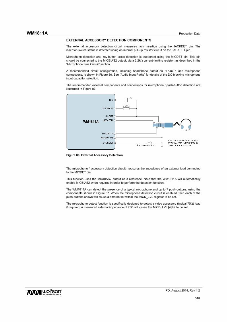
WM1811A Production Data
w PD, August 2014, Rev 4.2
318
EXTERNAL ACCESSORY DETECTION COMPONENTS
The external accessory detection circuit measures jack insertion using the JACKDET pin. The insertion switch status is detected using an internal pull-up resistor circuit on the JACKDET pin.
Microphone detection and key-button press detection is supported using the MICDET pin. This pin should be connected to the MICBIAS2 output, via a 2.2k current-limiting resistor, as described in the “Microphone Bias Circuit” section.
A recommended circuit configuration, including headphone output on HPOUT1 and microphone connections, is shown in Figure 86. See “Audio Input Paths” for details of the DC-blocking microphone input capacitor selection.
The recommended external components and connections for microphone / push-button detection are illustrated in Figure 87.
Figure 86 External Accessory Detection
The microphone / accessory detection circuit measures the impedance of an external load connected to the MICDET pin.
This function uses the MICBIAS2 output as a reference. Note that the WM1811A will automatically enable MICBIAS2 when required in order to perform the detection function.
The WM1811A can detect the presence of a typical microphone and up to 7 push-buttons, using the components shown in Figure 87. When the microphone detection circuit is enabled, then each of the push-buttons shown will cause a different bit within the MICD_LVL register to be set.
The microphone detect function is specifically designed to detect a video accessory (typical 75) load if required. A measured external impedance of 75 will cause the MICD_LVL [4] bit to be set.

Production Data WM1811A
w PD, August 2014, Rev 4.2
319
Figure 87 Microphone / Push-Button External Components

WM1811A Production Data
w PD, August 2014, Rev 4.2
320
CLASS D SPEAKER CONNECTIONS
The WM1811A incorporates two Class D speaker drivers, which offer high amplifier efficiency at large signal levels. As the Class D output is a pulse width modulated signal, the choice of speakers and tracking of signals is critical for ensuring good performance and reducing EMI in this mode.
The efficiency of the speaker drivers is affected by the series resistance between the WM1811A and the speaker (e.g. PCB track loss and inductor ESR) as shown in Figure 88. This resistance should be as low as possible to maximise efficiency.
Figure 88 Speaker Connection Losses
The Class D output requires external filtering in order to recreate the audio signal. This may be implemented using a 2nd order LC or 1st order RC filter, or else may be achieved by using a loudspeaker whose internal inductance provides the required filter response. An LC or RC filter should be used if the loudspeaker characteristics are unknown or unsuitable, or if the length of the loudspeaker connection is likely to lead to EMI problems.
In applications where it is necessary to provide Class D filter components, a 2nd order LC filter is the recommended solution as it provides more attenuation at higher frequencies and minimises power dissipated in the filter when compared to a first order RC filter (lower ESR). This maximises both rejection of unwanted switching frequencies and overall speaker efficiency. A suitable implementation is illustrated in Figure 89.
Figure 89 Class D Output Filter Components

Production Data WM1811A
w PD, August 2014, Rev 4.2
321
A simple equivalent circuit of a loudspeaker consists of a serially connected resistor and inductor, as shown in Figure 90. This circuit provides a low pass filter for the speaker output. If the loudspeaker characteristics are suitable, then the loudspeaker itself can be used in place of the filter components described earlier. This is known as ‘filterless’ operation.
Figure 90 Speaker Equivalent Circuit for Filterless Operation
For filterless Class D operation, it is important to ensure that a speaker with suitable inductance is chosen. For example, if we know the speaker impedance is 8Ω and the desired cut-off frequency is 20kHz, then the optimum speaker inductance may be calculated as:
8 loudspeakers typically have an inductance in the range 20H to 100H, however, it should be noted that a loudspeaker inductance will not be constant across the relevant frequencies for Class D operation (up to and beyond the Class D switching frequency). Care should be taken to ensure that the cut-off frequency of the loudspeaker’s filtering is low enough to suppress the high frequency energy of the Class D switching and, in so doing, to prevent speaker damage. The Class D outputs of the WM1811A operate at much higher frequencies than is recommended for most speakers and it must be ensured that the cut-off frequency is low enough to protect the speaker.
RECOMMENDED EXTERNAL COMPONENTS DIAGRAM
Figure 91provides a summary of recommended external components for WM1811A. Note that this diagram does not include any components that are specific to the end application e.g. it doesnot include filtering on the speaker outputs (assume filterless Class D operation), RF decoupling, or RF filtering for pins which connect to the external world i.e. headphone or speaker outputs.

WM1811A Production Data
w PD, August 2014, Rev 4.2
322
WM1811A
SPKGND2
CPVDD
AVDD1
SPKVDD2
DGND
CPGND
AGND
MCLK1
DACDAT1
LRCLK1
BCLK1
ADCDAT1
SDA
SCLK
IN1LP
IN1RP
IN2LN/DMICDAT
IN2LP/VRXN
IN1RN
IN1LN
IN2RP/VRXP
IN2RN
MICBIAS1
VMIDC
MICBIAS2
HPOUT2N
HPOUT2P
HPOUT1L
HPOUT1FB
HPOUT1R
LINEOUT1N
LINEOUT2P
LINEOUT2N
LINEOUT1P
LINEOUTFB
SPKOUTLN
SPKOUTRP
SPKOUTRN
SPKOUTLP
CPCA
CPVOUTP
CPVOUTN
CPCB
2.2 F
2.2 F 2.2 F
Loudspeaker
EarpieceSpeaker
4.7 F
MICBIAS1
Headset
1 F
1 F
1 F
1 F
4.7 F0.1 F
4.7 F
4.7 F
Vbat 1.8V
Audio Interface 1
Control Interface
1 F
1 F
1 F
1 F
SPKMODE
Loudspeaker
3.0V (LDO1)
MCLK2Master Clocks
ADCLRCLK1/GPIO1
DACDAT2
LRCLK2
BCLK2
ADCDAT2
Audio Interface 2
GPIO8/DACDAT3
GPIO10/LRCLK3
GPIO11/BCLK3
GPIO9/ADCDAT3
Audio Interface 3
ADDR
LDO1ENA
LDO2ENALDO Control
VREFC1 F
DMICCLKDigital MIC clock
HP2GND
LDO1VDD
REFGND
0.1 F
(Note: HPOUT1FB ground connection close to headset jack)
DBVDD1
DBVDD2
DBVDD31 F
MICBIAS2
MICDET
1 F
1 F
1 F
1 F
Analogue Audio (Mic / Line) Inputs
Note that the optimum input capacitance will vary according to the required frequency response and the applicable input impedance.
Note that input capacitors are not required for connection to Digital Microphone (DMIC) components.
4.7 F
Line Outputs (can be configured as Differential pairs or Stereo pairs).
Note that the optimum output capacitance will vary according to the required frequency response.
The ground feedback connection to LINEOUTFB is optional.
Speaker Mode Select
SPKVDD1
SPKGND1
AVDD2
DCVDD
1 F
1.05V (LDO2)
JACKDET
Figure 91 Recommended External Components Diagram

Production Data WM1811A
w PD, August 2014, Rev 4.2
323
DIGITAL AUDIO INTERFACE CLOCKING CONFIGURATIONS
The WM1811A provides 3 digital audio interfaces and supports many different clocking configurations. The asynchronous sample rate converter enables more than one digital audio interface to be supported simultaneously, even when there is no synchronisation between these interfaces. In a typical application, this enables audio mixing between a multimedia applications processor and a baseband voice call processor, for example.
The AIF1 and AIF2 audio interfaces can be configured in Master or Slave modes, and can also support defined combinations of mixed sample rates. In all applications, it is important that the system clocking configuration is correctly designed. Incorrect clock configurations will lead to audible clicks arising from dropped or repeated audio samples; this is caused by the inherent tolerances of multiple asynchronous system clocks.
To ensure reliable clocking of the audio interface functions, it is a requirement that, for each audio interface, the external interface clocks (eg. BCLK, LRCLK) are derived from the same clock source as the respective AIF clock (AIFnCLK).
In AIF Master mode, the external BCLK and LRCLK signals are generated by the WM1811A and synchronisation of these signals with AIFnCLK is guaranteed. In this case, clocking of the AIF is derived from the MCLK1 or MCLK2 inputs, either directly or via one of the Frequency Locked Loop (FLL) circuits.
In AIF Slave mode, the external BCLK and LRCLK signals are generated by another device, as inputs to the WM1811A. In this case, it must be ensured that the respective AIF clock is generated from a source that is synchronised to the external BCLK and LRCLK inputs. In a typical Slave mode application, the BCLK input is selected as the clock reference, using the FLL to perform frequency shifting. It is also possible to use the MCLK1 or MCLK2 inputs, but only if the selected clock is synchronised externally to the BCLK and LRCLK inputs.
The valid AIF clocking configurations are listed in Table 139 for AIF Master and AIF Slave modes.
AUDIO INTERFACE MODE CLOCKING CONFIGURATION
AIF Master Mode AIFnCLK_SRC selects FLL1 or FLL2 as AIFnCLK source; FLLn_REFCLK_SRC selects MCLK1 or MCLK2 as FLLn source.
AIFnCLK_SRC selects MCLK1 or MCLK2 as AIFnCLK source.
AIF Slave Mode AIFnCLK_SRC selects FLL1 or FLL2 as AIFnCLK source; FLLn_REFCLK_SRC selects BCLKn as FLLn source.
AIFnCLK_SRC selects MCLK1 or MCLK2 as AIFnCLK source, provided MCLK is externally synchronised to the BCLKn input.
AIFnCLK_SRC selects FLL1 or FLL2 as AIFnCLK source; FLLn_REFCLK_SRC selects MCLK1 or MCLK2 as FLLn source, provided MCLK is externally synchronised to the BCLKn input.
Table 139 Audio Interface Clocking Confgurations
In each case, the AIFnCLK frequency must be a valid ratio to the LRCLKn frequency; the supported clocking ratios are defined by the AIFnCLK_RATE register.
The valid AIF clocking configurations are illustrated in Figure 92 to Figure 96below.Note that, where MCLK1 is illustrated as the clock source, it is equally possible to select MCLK2 as the clock source. Similarly, in cases where FLL1 is illustrated, it is equally possible to select the FLL2.

WM1811A Production Data
w PD, August 2014, Rev 4.2
324
Figure 92 AIF Master Mode, using MCLK as Reference
Figure 93 AIF Master Mode, using MCLK and FLL as Reference
Figure 94 AIF Slave Mode, using BCLK and FLL as Reference
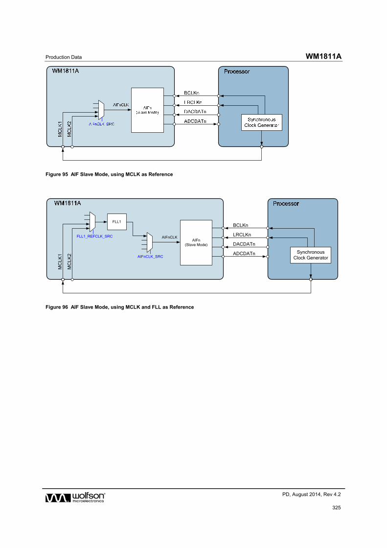
Production Data WM1811A
w PD, August 2014, Rev 4.2
325
Figure 95 AIF Slave Mode, using MCLK as Reference
MC
LK1
MC
LK2
AIFnCLKAIFn
(Slave Mode)
BCLKn
LRCLKn
DACDATn
ADCDATnAIFnCLK_SRC
FLL1_REFCLK_SRC
FLL1
Synchronous Clock Generator
Figure 96 AIF Slave Mode, using MCLK and FLL as Reference

WM1811A Production Data
w PD, August 2014, Rev 4.2
326
PCB LAYOUT CONSIDERATIONS
Poor PCB layout will degrade the performance and be a contributory factor in EMI, ground bounce and resistive voltage losses. All external components should be placed as close to the WM1811A device as possible, with current loop areas kept as small as possible. Specific factors relating to Class D loudspeaker connection are detailed below.
CLASS D LOUDSPEAKER CONNECTION
Long, exposed PCB tracks or connection wires will emit EMI. The distance between the WM1811A and the loudspeaker should therefore be kept as short as possible. Where speakers are connected to the PCB via a cable form, it is recommended that a shielded twisted pair cable is used. The shield should be connected to the main system, with care taken to ensure ground loops are avoided.
Further reduction in EMI can be achieved using PCB ground (or VDD) planes and also by using passive LC components to filter the Class D switching waveform. When passive filtering is used, low ESR components should be chosen in order to minimise the series resistance between the WM1811A and the speaker, maximising the power efficiency.
LC passive filtering will usually be effective at reducing EMI at frequencies up to around 30MHz. To reduce emissions at higher frequencies, ferrite beads can also be used. These should be positioned as close to the device as possible.
These techniques for EMI reduction are illustrated in Figure 97.
SPKP
SPKNEMI
SPKP
SPKN
SPKP
SPKN
LOW ESR
LOW ESR
SPKP
SPKN
SPKP
SPKN
Long, exposed tracks emit EMI
Short connection wires will reduce EMI emission
Shielding using PCB ground (or VDD) planes will reduce EMI emission
LC filtering will reduce EMI emission up to around 30MHz
Ferrite beads will reduce EMI emission at frequencies above 30MHz.
Figure 97 EMI Reduction Techniques
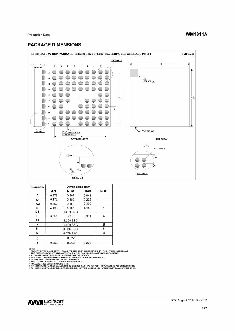
Production Data WM1811A
w PD, August 2014, Rev 4.2
327
PACKAGE DIMENSIONS
B: 80 BALL W-CSP PACKAGE 4.158 X 3.876 X 0.607 mm BODY, 0.40 mm BALL PITCH
A1 CORNER
TOP VIEW
E
4
DETAIL 2
DETAIL 2
A
A22
A
DETAIL 1
D
C
B
G
F
E
e
e
BOTTOM VIEW
16 5 4 3 2
G
NOTES: 1. PRIMARY DATUM -Z- AND SEATING PLANE ARE DEFINED BY THE SPHERICAL CROWNS OF THE SOLDER BALLS.2. THIS DIMENSION INCLUDES STAND-OFF HEIGHT ‘A1’, SILICON THICKNESS AND BACKSIDE COATING.3. A1 CORNER IS IDENTIFIED BY INK/LASER MARK ON TOP PACKAGE.4. BILATERAL TOLERANCE ZONE IS APPLIED TO EACH SIDE OF THE PACKAGE BODY.5. ‘e’ REPRESENTS THE BASIC SOLDER BALL GRID PITCH.6. THIS DRAWING IS SUBJECT TO CHANGE WITHOUT NOTICE.7. FOLLOWS JEDEC DESIGN GUIDE MO-211-C.8. f1 = NOMINAL DISTANCE OF BALL CENTRE TO DIE EDGE X AXIS (AS PER POD) – APPLICABLE TO ALL CORNERS OF DIE.9. f2 = NOMINAL DISTANCE OF DIE CENTRE TO DIE EDGE IN Y AXIS (AS PER POD) – APPLICABLE TO ALL CORNERS OF DIE.
7
H
89
DM095.B
A1 0.172
DD1
E
E1e
3.600 BSC
3.876
3.200 BSC
0.400 BSC
4.158
Dimensions (mm)Symbols
MIN NOM MAX NOTE
A 0.607
A2 0.367 0.383 0.399
5f1
0.6410.573
0.202 0.232
g 0.022
h 0.262
f2
0.338 BSC
0.279 BSC
8
9
4.133
3.851
4.183
3.901
E1
J
K
DD1
A1
Z0.06
Z
SOLDER BALL
f1
f2
h
DETAIL 1
0.025 4 X
1
3
4
4
4
0.258 0.266
0.015 C A BM
0.004 CM

WM1811A Production Data
w PD, August 2014, Rev 4.2
328
IMPORTANT NOTICE
Wolfson Microelectronics plc (“Wolfson”) products and services are sold subject to Wolfson’s terms and conditions of sale, delivery and payment supplied at the time of order acknowledgement.
Wolfson warrants performance of its products to the specifications in effect at the date of shipment. Wolfson reserves the right to make changes to its products and specifications or to discontinue any product or service without notice. Customers should therefore obtain the latest version of relevant information from Wolfson to verify that the information is current.
Testing and other quality control techniques are utilised to the extent Wolfson deems necessary to support its warranty. Specific testing of all parameters of each device is not necessarily performed unless required by law or regulation.
In order to minimise risks associated with customer applications, the customer must use adequate design and operating safeguards to minimise inherent or procedural hazards. Wolfson is not liable for applications assistance or customer product design. The customer is solely responsible for its selection and use of Wolfson products. Wolfson is not liable for such selection or use nor for use of any circuitry other than circuitry entirely embodied in a Wolfson product.
Wolfson’s products are not intended for use in life support systems, appliances, nuclear systems or systems where malfunction can reasonably be expected to result in personal injury, death or severe property or environmental damage. Any use of products by the customer for such purposes is at the customer’s own risk.
Wolfson does not grant any licence (express or implied) under any patent right, copyright, mask work right or other intellectual property right of Wolfson covering or relating to any combination, machine, or process in which its products or services might be or are used. Any provision or publication of any third party’s products or services does not constitute Wolfson’s approval, licence, warranty or endorsement thereof. Any third party trade marks contained in this document belong to the respective third party owner.
Reproduction of information from Wolfson datasheets is permissible only if reproduction is without alteration and is accompanied by all associated copyright, proprietary and other notices (including this notice) and conditions. Wolfson is not liable for any unauthorised alteration of such information or for any reliance placed thereon.
Any representations made, warranties given, and/or liabilities accepted by any person which differ from those contained in this datasheet or in Wolfson’s standard terms and conditions of sale, delivery and payment are made, given and/or accepted at that person’s own risk. Wolfson is not liable for any such representations, warranties or liabilities or for any reliance placed thereon by any person.
ADDRESS:
Wolfson Microelectronics plc
26 Westfield Road
Edinburgh
EH11 2QB
United Kingdom
Tel :: +44 (0)131 272 7000
Fax :: +44 (0)131 272 7001
Email :: [email protected]
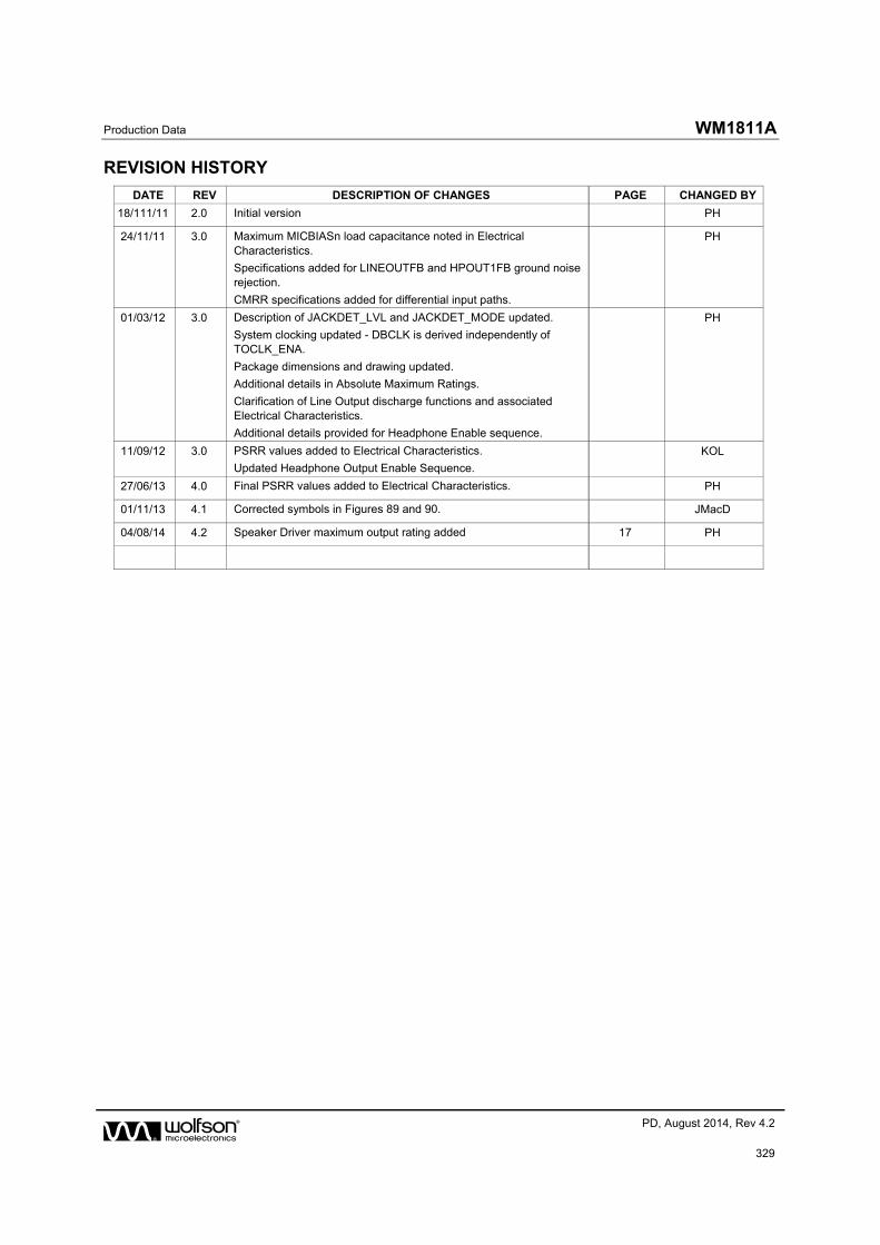
Production Data WM1811A
w PD, August 2014, Rev 4.2
329
REVISION HISTORY
DATE REV DESCRIPTION OF CHANGES PAGE CHANGED BY
18/111/11 2.0 Initial version PH
24/11/11 3.0 Maximum MICBIASn load capacitance noted in Electrical Characteristics.
Specifications added for LINEOUTFB and HPOUT1FB ground noise rejection.
CMRR specifications added for differential input paths.
PH
01/03/12 3.0 Description of JACKDET_LVL and JACKDET_MODE updated.
System clocking updated - DBCLK is derived independently of TOCLK_ENA.
Package dimensions and drawing updated.
Additional details in Absolute Maximum Ratings.
Clarification of Line Output discharge functions and associated Electrical Characteristics.
Additional details provided for Headphone Enable sequence.
PH
11/09/12 3.0 PSRR values added to Electrical Characteristics.
Updated Headphone Output Enable Sequence.
KOL
27/06/13 4.0 Final PSRR values added to Electrical Characteristics. PH
01/11/13 4.1 Corrected symbols in Figures 89 and 90. JMacD
04/08/14 4.2 Speaker Driver maximum output rating added 17 PH