Multi-Boot Usage Guide for Nexus Platform
36
Multi-Boot Usage Guide for Nexus Platform Technical Note FPGA-TN-02145-1.1 May 2020
Transcript of Multi-Boot Usage Guide for Nexus Platform

Multi-Boot Usage Guide for Nexus Platform
Technical Note
FPGA-TN-02145-1.1
May 2020

Multi-Boot Usage Guide for Nexus Platform Technical Note
© 2020 Lattice Semiconductor Corp. All Lattice trademarks, registered trademarks, patents, and disclaimers are as listed at www.latticesemi.com/legal. All other brand or product names are trademarks or registered trademarks of their respective holders. The specifications and information herein are subject to change without notice.
2 FPGA-TN-02145-1.1
Disclaimers Lattice makes no warranty, representation, or guarantee regarding the accuracy of information contained in this document or the suitability of its products for any particular purpose. All information herein is provided AS IS and with all faults, and all risk associated with such information is entirely with Buyer. Buyer shall not rely on any data and performance specifications or parameters provided herein. Products sold by Lattice have been subject to limited testing and it is the Buyer's responsibility to independently determine the suitability of any products and to test and verify the same. No Lattice products should be used in conjunction with mission- or safety-critical or any other application in which the failure of Lattice’s product could create a situation where personal injury, death, severe property or environmental damage may occur. The information provided in this document is proprietary to Lattice Semiconductor, and Lattice reserves the right to make any changes to the information in this document or to any products at any time without notice.

Multi-Boot Usage Guide for Nexus Platform Technical Note
© 2020 Lattice Semiconductor Corp. All Lattice trademarks, registered trademarks, patents, and disclaimers are as listed at www.latticesemi.com/legal. All other brand or product names are trademarks or registered trademarks of their respective holders. The specifications and information herein are subject to change without notice.
FPGA-TN-02145-1.1 3
Contents Glossary ................................................................................................................................................................................ 4 1. Introduction .................................................................................................................................................................. 5 2. Resources ...................................................................................................................................................................... 6 3. CrossLink-NX/Certus-NX Dual Boot Mode .................................................................................................................... 9
3.1. Description of the CrossLink-NX/Certus-NX Dual Boot Flow Diagram .............................................................. 10 4. CrossLink-NX/Certus-NX Ping-Pong Boot Mode ......................................................................................................... 11
4.1. Description of the CrossLink-NX/Certus-NX Ping-Pong Boot Flow Diagram ..................................................... 12 5. CrossLink-NX/Certus-NX Multi-Boot Mode ................................................................................................................ 13 6. Creating a PROM File .................................................................................................................................................. 14
6.1. Using Radiant Deployment Tool to Create a Dual Boot PROM Hex File ........................................................... 14 6.2. Using the Lattice Deployment Tool to Create a Ping-Pong Boot PROM Hex File .............................................. 19 6.3. Using Radiant Deployment Tool to Create a Multi-Boot PROM Hex File .......................................................... 24
7. Programming the Dual Boot, Ping-Pong Boot, or Multi-Boot Pattern into the SPI Flash Device ............................... 31 Technical Support Assistance ............................................................................................................................................. 34 Revision History .................................................................................................................................................................. 35
Figures Figure 3.1. CrossLink-NX/Certus-NX Dual Boot Flow Diagram ............................................................................................. 9 Figure 4.1. CrossLink-NX/Certus-NX Ping-Pong Boot Flow Diagram ................................................................................... 11 Figure 6.1. Creating New Deployment for Dual Boot PROM Hex File ................................................................................ 14 Figure 6.2. Select Input Files Window ................................................................................................................................ 15 Figure 6.3. Dual Boot Options Window .............................................................................................................................. 16 Figure 6.4. Select Output File Window ............................................................................................................................... 17 Figure 6.5. Generate Deployment Window ........................................................................................................................ 18 Figure 6.6. Creating New Deployment for Ping-Pong Boot PROM Hex File ....................................................................... 19 Figure 6.7. Select Input Files Window ................................................................................................................................ 20 Figure 6.8. Ping-Pong Boot Options Window ..................................................................................................................... 21 Figure 6.9. Select Output File Window ............................................................................................................................... 22 Figure 6.10. Generate Deployment Window ...................................................................................................................... 23 Figure 6.11. Creating New Deployment for Multi-Boot ..................................................................................................... 24 Figure 6.12. Select Input File Window ................................................................................................................................ 25 Figure 6.13. Advanced SPI Flash Options – Options Tab Window ...................................................................................... 27 Figure 6.14. Advanced SPI Flash Options – Multiple Boot Tab Window ............................................................................ 28 Figure 6.15. Select Output File Window ............................................................................................................................. 29 Figure 6.16. Generate Deployment Window ...................................................................................................................... 30 Figure 7.1. Radiant Programmer – Getting Started Window.............................................................................................. 32 Figure 7.2. Radiant Programmer – Device Properties Window .......................................................................................... 33
Tables Table 2.1. Maximum Configuration Bitstream Size – Single Bitstream Boot Mode ............................................................. 6 Table 2.2. Maximum Configuration Bitstream Size – Dual Boot Mode/Ping-Pong Mode .................................................... 7 Table 2.3. Maximum Configuration Bitstream Size – Multi-Boot Mode .............................................................................. 8 Table 3.1. Control Register 1 [3:2] – Master Preamble Timer Retry Value ........................................................................ 10 Table 4.1. Control Register 1 [3:2] – Master Preamble Timer Retry Value ........................................................................ 12

Multi-Boot Usage Guide for Nexus Platform Technical Note
© 2020 Lattice Semiconductor Corp. All Lattice trademarks, registered trademarks, patents, and disclaimers are as listed at www.latticesemi.com/legal. All other brand or product names are trademarks or registered trademarks of their respective holders. The specifications and information herein are subject to change without notice.
4 FPGA-TN-02145-1.1
Glossary A glossary of terms used in this document.
Acronym Definition
Alternative Boot After the FPGA device has been configured, this pattern is loaded when the PROGRAMN pin is toggled or the Refresh instruction is issued. Up to four Alternative Boot patterns are possible.
Binary Hex Data File (.bin File)
The data image of the Hex data file in binary format. All Hex data files are converted into this format prior to consumption. This type of file is not printable.
Bitstream Data File (.bit File)
The configuration data file, for a single FPGA device, in the format that can be loaded directly into the FPGA device to configure the SRAM cells. The file is expressed in binary Hex format. The file is not printable.
Configure Write the pattern into the SRAM fuses of the FPGA device and wake up.
Dual Boot The device has two patterns, a Primary pattern and a Golden pattern, to choose to load.
EBR Embedded Block RAM
FD-SOI (Fully Depleted Silicon On Insulator)
A process that uses an ultra-thin buried oxide layer.
Flash Lock
The feature provides protection to the Flash fuses against accidental erase or corruption. Most of the SPI Flash devices support Soft Lock. Lock choices include:
Whole device
Bottom half
Bottom quarter
Last sector
Details can be found in the SPI Flash device data sheet.
Golden Boot The guaranteed good pattern loaded into the FPGA device when booting failure occurs. It is also known as the root boot. Only one Golden Boot pattern is allowed.
Hex Data File (.exo, .mcs, .xtek Files)
The data record files that are in the format commonly known as Intel Hex, Motorola Hex or Extended Tektronix Hex. They are also known as addressed record files. The advantages include its small size and it is printable, and thus good for record keeping. This type of file is not directly consumable by the utilities supporting it.
LRAM Large RAM
Multi-Boot
Multiple Boot
The device has more than two patterns, a Primary pattern, a Golden pattern and some Alternative patterns, to choose to load.
Primary Boot Upon power cycling, the FPGA device will load this pattern in first. Only one Primary pattern is allowed.
Program Writes into the selected Flash cells state a logical zero (0) (close fuse).
Refresh The action loads the pattern from a non-volatile source to configure the FPGA device.
SPI Stands for the Serial Peripheral Interface defined originally by Motorola.
Sector (Block) The smallest number of bytes of Flash fuses can be erased at the same time by the erase command.

Multi-Boot Usage Guide for Nexus Platform Technical Note
© 2020 Lattice Semiconductor Corp. All Lattice trademarks, registered trademarks, patents, and disclaimers are as listed at www.latticesemi.com/legal. All other brand or product names are trademarks or registered trademarks of their respective holders. The specifications and information herein are subject to change without notice.
FPGA-TN-02145-1.1 5
1. Introduction CrossLink™-NX and Certus™-NX families of low-power FPGAs can be used in a wide range of applications, and are optimized for bridging and processing needs in the Embedded Vision space. It is built on Lattice Nexus FPGA platform, using low-power 28-nm FD-SOI technology. CrossLink-NX and Certus-NX families support various booting options for loading the configuration SRAM from a non-volatile memory for configuration flexibility and fail-safe configuration.
The CrossLink-NX and Certus-NX families support various configuration boot modes to mitigate risk during the field upgrade process and to allow flexibility of executing different patterns. Field upgrade disruptions may occur due to power disruption, communication interruption or bitstream pattern corruption. The CrossLink-NX and Certus-NX families support the following boot modes through its Master SPI interface:
Dual Boot mode – Switches to load from the second known good (Golden) pattern when the first pattern becomes corrupted.
Ping-Pong Boot mode – Switches between two bitstream patterns based on your choice. If the system fails to boot from one of the bitstreams, it automatically boots from the second bitstream.
Multi-Boot mode – Allows the system to dynamically switch between two to five bitstream patterns while still being protected with a Golden (sixth) pattern.
The CrossLink-NX and Certus-NX families support these boot modes by combining all the bitstream patterns into a single boot image and storing it in a single external SPI Flash device. This solution decreases cost, reduces board space and simplifies field grades.

Multi-Boot Usage Guide for Nexus Platform Technical Note
© 2020 Lattice Semiconductor Corp. All Lattice trademarks, registered trademarks, patents, and disclaimers are as listed at www.latticesemi.com/legal. All other brand or product names are trademarks or registered trademarks of their respective holders. The specifications and information herein are subject to change without notice.
6 FPGA-TN-02145-1.1
2. Resources The CrossLink-NX and Certus-NX families are SRAM-based FPGAs. The volatile SRAM configuration memory must be loaded from an external non-volatile memory that can store all of the configuration data. The size of the configuration data is based on the amount of logic available in the FPGA, number of pre-initialized Embedded Block RAM (EBR) components and number of pre-initialized Large RAM Block (LRAM) components. A CrossLink-NX/Certus-NX design using the largest device, with every EBR and LRAM pre-initialized with unique data values and generated without compression requires the largest amount of storage. The minimum SPI Flash densities required to support the different configuration boot modes are listed in Table 2.1, Table 2.2, and Table 2.3.
Table 2.1. Maximum Configuration Bitstream Size – Single Bitstream Boot Mode
Device Configuration
Uncompressed1 SPI Mode
Single Bitstream Size (Mb) Minimum SPI Flash Size
(Mb)
LIFCL-17
No LRAM, No EBR TBD TBD
No LRAM, MAX EBR TBD TBD
MAX LRAM, No EBR TBD TBD
MAX LRAM, MAX EBR TBD TBD
LIFCL-40
No LRAM, No EBR 6.170 8
No LRAM, MAX EBR 7.865 8
MAX LRAM, No EBR 7.365 8
MAX LRAM, MAX EBR 8.965 16
LFD2NX-17
No LRAM, No EBR TBD TBD
No LRAM, MAX EBR TBD TBD
MAX LRAM, No EBR TBD TBD
MAX LRAM, MAX EBR TBD TBD
LFD2NX-40
No LRAM, No EBR TBD TBD
No LRAM, MAX EBR TBD TBD
MAX LRAM, No EBR TBD TBD
MAX LRAM, MAX EBR TBD TBD
Note: 1. CrossLink-NX/Certus-NX family of devices support bitstream compression. Compression ratio depends on the bitstream.
Therefore, Table 2.1 only provides uncompressed bitstream data.

Multi-Boot Usage Guide for Nexus Platform Technical Note
© 2020 Lattice Semiconductor Corp. All Lattice trademarks, registered trademarks, patents, and disclaimers are as listed at www.latticesemi.com/legal. All other brand or product names are trademarks or registered trademarks of their respective holders. The specifications and information herein are subject to change without notice.
FPGA-TN-02145-1.1 7
Table 2.2. Maximum Configuration Bitstream Size – Dual Boot Mode/Ping-Pong Mode
Device Configuration
Uncompressed1 SPI Mode
Single Bitstream
Size (Mb)
Two Bitstreams
Size (Mb)
Minimum SPI Flash
Size (Mb)
LIFCL-17
No LRAM, No EBR TBD TBD TBD
No LRAM, MAX EBR TBD TBD TBD
MAX LRAM, No EBR TBD TBD TBD
MAX LRAM, MAX EBR TBD TBD TBD
LIFCL-40
No LRAM, No EBR 6.170 12.340 16
No LRAM, MAX EBR 7.865 15.730 16
MAX LRAM, No EBR 7.365 14.730 16
MAX LRAM, MAX EBR 8.965 17.930 32
LFD2NX-17
No LRAM, No EBR TBD TBD TBD
No LRAM, MAX EBR TBD TBD TBD
MAX LRAM, No EBR TBD TBD TBD
MAX LRAM, MAX EBR TBD TBD TBD
LFD2NX-40
No LRAM, No EBR TBD TBD TBD
No LRAM, MAX EBR TBD TBD TBD
MAX LRAM, No EBR TBD TBD TBD
MAX LRAM, MAX EBR TBD TBD TBD
Note: 1. CrossLink-NX/Certus-NX family of devices support bitstream compression. Compression ratio depends on the bitstream.
Therefore, Table 2.2 only provides uncompressed bitstream data.

Multi-Boot Usage Guide for Nexus Platform Technical Note
© 2020 Lattice Semiconductor Corp. All Lattice trademarks, registered trademarks, patents, and disclaimers are as listed at www.latticesemi.com/legal. All other brand or product names are trademarks or registered trademarks of their respective holders. The specifications and information herein are subject to change without notice.
8 FPGA-TN-02145-1.1
Table 2.3. Maximum Configuration Bitstream Size – Multi-Boot Mode
Device Configuration
Uncompressed1 3 Bitstream Patterns2
4 Bitstream Patterns2
5 Bitstream Patterns2
6 Bitstream Patterns2
Single Bitstream Size
(Mb) Minimum SPI Flash Size (Mb)
LIFCL-17
No LRAM, No EBR TBD TBD TBD TBD TBD TBD TBD TBD TBD
No LRAM, MAX EBR TBD TBD TBD TBD TBD TBD TBD TBD TBD
MAX LRAM, No EBR TBD TBD TBD TBD TBD TBD TBD TBD TBD
MAX LRAM, MAX EBR TBD TBD TBD TBD TBD TBD TBD TBD TBD
LIFCL-40
No LRAM, No EBR 6.170 18.510 32 24.680 32 30.850 32 37.020 64
No LRAM, MAX EBR 7.865 23.595 32 31.460 32 39.325 64 47.190 64
MAX LRAM, No EBR 7.365 22.095 32 29.460 32 36.825 64 44.190 64
MAX LRAM, MAX EBR 8.965 26.895 32 35.860 64 44.825 64 53.790 64
LFD2NX-17
No LRAM, No EBR TBD TBD TBD TBD TBD TBD TBD TBD TBD
No LRAM, MAX EBR TBD TBD TBD TBD TBD TBD TBD TBD TBD
MAX LRAM, No EBR TBD TBD TBD TBD TBD TBD TBD TBD TBD
MAX LRAM, MAX EBR TBD TBD TBD TBD TBD TBD TBD TBD TBD
LFD2NX-40
No LRAM, No EBR TBD TBD TBD TBD TBD TBD TBD TBD TBD
No LRAM, MAX EBR TBD TBD TBD TBD TBD TBD TBD TBD TBD
MAX LRAM, No EBR TBD TBD TBD TBD TBD TBD TBD TBD TBD
MAX LRAM, MAX EBR TBD TBD TBD TBD TBD TBD TBD TBD TBD
Notes: 1. CrossLink-NX/Certus-NX family of devices support bitstream compression. Compression ratio depends on the bitstream.
Therefore, Table 2.3 only provides uncompressed bitstream data. 2. Includes Golden bitstream pattern.

Multi-Boot Usage Guide for Nexus Platform Technical Note
© 2020 Lattice Semiconductor Corp. All Lattice trademarks, registered trademarks, patents, and disclaimers are as listed at www.latticesemi.com/legal. All other brand or product names are trademarks or registered trademarks of their respective holders. The specifications and information herein are subject to change without notice.
FPGA-TN-02145-1.1 9
3. CrossLink-NX/Certus-NX Dual Boot Mode The CrossLink-NX/Certus-NX Dual Boot mode supports booting from two configuration patterns that reside in an external SPI Flash device. One pattern is designated as the Primary pattern, and the second pattern is designated as the Golden pattern. When the CrossLink-NX/Certus-NX part boots up, it attempts to boot from the Primary pattern. If loading of the Primary pattern fails, the CrossLink-NX/Certus-NX part boots from the Golden pattern.
Set Count = 0Send Read Opcode
Send Address 0
No
PASS
Release DONE PinWake-Up
Error?No
Yes
FAIL
Drive INITN Low
Pream bleDetect?
No
Yes
JUMPCommand?
No
Yes
Co unt > 1?YesNo
Load Golden Data
Continue ReadingSPI
PASSPASS
Error?
FAILFAIL
PreambleDetected?
JUMPCommand?
Yes
Count > 1?YesYesNo
SPI Flash
Load Golden Pattern
Load Primary Pattern
Address 0
Address X
Primary Pattern
JUMP Instruction
Read JUMP Command & Golden Pattern Address
FPGA
POR
YesRetry
Golden Pattern
Start Reading SPI Address X
Start Reading SPI Address 0
Send Read OpcodeSend Address JUMP
Count = Count + 1
Figure 3.1. CrossLink-NX/Certus-NX Dual Boot Flow Diagram

Multi-Boot Usage Guide for Nexus Platform Technical Note
© 2020 Lattice Semiconductor Corp. All Lattice trademarks, registered trademarks, patents, and disclaimers are as listed at www.latticesemi.com/legal. All other brand or product names are trademarks or registered trademarks of their respective holders. The specifications and information herein are subject to change without notice.
10 FPGA-TN-02145-1.1
3.1. Description of the CrossLink-NX/Certus-NX Dual Boot Flow Diagram This flow is triggered either by power cycle, the PROGRAMN pin being toggled, or by the REFRESH instruction being received.
When the Dual Boot mode is selected, in addition to the standard CRC check, a time-out check is performed while reading the Primary pattern, the Golden pattern, and the JUMP command.
Time-Out Check – CrossLink-NX/Certus-NX device searches for the preamble code 0xBDCD (0xBDB3 when Byte Wide Bit Mirror is enabled) from the Primary Pattern as part of the configuration protocol. The number of retries the CrossLink-NX/Certus-NX device attempts is defined in Control Register 1 [3:2] (Table 3.1).
Data Corruption Check – After the detection of the preamble code, the CRC engine is turned on to detect whether or not the bitstream is corrupted. This determines whether the SPI Flash device has a corrupted Primary pattern or Golden pattern due to SPI Flash program disruption or data loss.
Table 3.1. Control Register 1 [3:2] – Master Preamble Timer Retry Value
Bit 3 Bit 2
No retry 0 0
Retry 1 time 0 1
Retry 3 times 1 0
Reserved 1 1
If the Primary pattern fails one of the two checks above, the CrossLink-NX/Certus-NX device knows that the Primary pattern is not valid. It drives the INITN pin LOW briefly to indicate an error and resets the configuration engine. After clearing all the SRAM fuses, it drives the INITN pin HIGH, and reads the JUMP command that directs it to the location of the Golden pattern in the SPI Flash.
If the JUMP command is corrupted, it also causes a configuration failure. It is important to note that a corrupted Golden pattern is not the only possible cause for Dual Boot configuration failure.
If the JUMP command is valid, the CrossLink-NX/Certus-NX device stops the SPI clock, drives the INITN pin LOW, resets the configuration engine, and performs a Clear All operation. The device then drives the INITN pin HIGH after the completion of the Clear All action, restarts the SPI clock, and reads the Golden pattern from the SPI Flash address designated in the JUMP command.
CrossLink-NX/Certus-NX device performs the same time-out check and CRC check when searching for the preamble code from the Golden pattern. If the Golden pattern is also corrupted, configuration fails. The CrossLink-NX/Certus-NX device stops driving the SPI clock, and the INITN pin is driven LOW.

Multi-Boot Usage Guide for Nexus Platform Technical Note
© 2020 Lattice Semiconductor Corp. All Lattice trademarks, registered trademarks, patents, and disclaimers are as listed at www.latticesemi.com/legal. All other brand or product names are trademarks or registered trademarks of their respective holders. The specifications and information herein are subject to change without notice.
FPGA-TN-02145-1.1 11
4. CrossLink-NX/Certus-NX Ping-Pong Boot Mode The CrossLink-NX/Certus-NX Ping-Pong Boot mode supports booting from two configuration patterns that reside in an external SPI Flash device. One pattern is designated as the Primary pattern and the second pattern is designated as the Secondary pattern. CrossLink-NX/Certus-NX boots from the pattern assigned in the Jump table. The Jump table allows the CrossLink-NX/Certus-NX device to boot from either the Primary pattern or the Secondary pattern without changing the physical location of the patterns within the SPI Flash. Only the Jump table needs to be updated to change the boot pattern. The other pattern, by default, becomes the Golden pattern.
Ba cku p JUM P In str uctio nNo
PASS
Error?No
Yes
FAIL
Drive INITN Low
Yes
JUMPCommand?
No
Yes
Continue ReadingSPI
PASSPASS
Error?
FAILFAIL
JUMPCommand?
Yes
SPI Flash
Secondary Pattern
Address 0
Address Y
JUMP Table
Read JUMP Command & Golden Pattern Address
FPGA
YesRetry
Primary Pattern
Address X
Load Primary Pattern
POR
Set Count = 0Send Read Opcode
Send Address 0
Read JUMP TableAddress 0
JUMP to Address X1
Start reading SPI
Start Reading SPI Address Y2
Load Secondary Pattern
Notes:1. Assumes Primary Pattern selected as First Boot option2. Secondary Pattern becomes the Golden Pattern in this configuration
Count > 1?
Count = Count + 1
Send Read Opcode Send Address JUMP
No Yes
PreambleDetected?
No
Release DONEWake-up
Figure 4.1. CrossLink-NX/Certus-NX Ping-Pong Boot Flow Diagram

Multi-Boot Usage Guide for Nexus Platform Technical Note
© 2020 Lattice Semiconductor Corp. All Lattice trademarks, registered trademarks, patents, and disclaimers are as listed at www.latticesemi.com/legal. All other brand or product names are trademarks or registered trademarks of their respective holders. The specifications and information herein are subject to change without notice.
12 FPGA-TN-02145-1.1
4.1. Description of the CrossLink-NX/Certus-NX Ping-Pong Boot Flow Diagram This flow is triggered either by power cycle, the PROGRAMN pin being toggled, or by the REFRESH instruction being received.
When Ping-Pong Boot mode is selected, in addition to the standard CRC checking, a time-out check is performed while reading the Primary pattern, the Secondary pattern, and the JUMP command.
Time-Out Check – CrossLink-NX/Certus-NX device searches for the preamble code 0xBDCD (0xBDB3 when Byte Wide Bit Mirror is enabled) from the pattern designated as “First Boot” selection as part of the configuration protocol. The number of retries CrossLink-NX/Certus-NX attempts is defined in Control Register 1 [3:2] (Table 4.1).
Data Corruption Check – After the detection of the preamble code, the CRC engine is turned on to detect whether the bitstream is corrupted. This will determine whether the SPI Flash device has a corrupted Primary or Secondary Pattern due to SPI Flash program disruption or data loss.
Table 4.1. Control Register 1 [3:2] – Master Preamble Timer Retry Value
Bit 3 Bit 2
No retry 0 0
Retry 1 time 0 1
Retry 3 times 1 0
Reserved 1 1
If the “First Boot” pattern fails one of the two checks above, the CrossLink-NX/Certus-NX device knows that the pattern is not valid. It drives the INITN pin LOW briefly to indicate an error and resets the configuration engine. After clearing all the SRAM fuses, it drives the INITN pin HIGH, and reads the JUMP command that directs it to the location of the other pattern, acting as the Golden pattern, in the SPI Flash.
If the JUMP command is corrupted, it also causes a configuration failure. It is important to note that a corrupted Golden pattern is not the only possible cause for Ping-ping mode configuration failure.
If the JUMP command is valid, the CrossLink-NX/Certus-NX device stops the SPI clock, drives the INITN pin LOW, resets the configuration engine, and performs a Clear All operation. The device then drives the INITN pin HIGH after the completion of the Clear All action, restarts the SPI clock, and reads the Golden pattern from the SPI Flash address designated in the JUMP command.
CrossLink-NX/Certus-NX device performs the same time-out check and the CRC check when searching for the preamble code from the Golden Pattern. If the Golden Pattern is also corrupted, configuration fails, stops driving the SPI clock, and the INITN pin is driven LOW.

Multi-Boot Usage Guide for Nexus Platform Technical Note
© 2020 Lattice Semiconductor Corp. All Lattice trademarks, registered trademarks, patents, and disclaimers are as listed at www.latticesemi.com/legal. All other brand or product names are trademarks or registered trademarks of their respective holders. The specifications and information herein are subject to change without notice.
FPGA-TN-02145-1.1 13
5. CrossLink-NX/Certus-NX Multi-Boot Mode CrossLink-NX/Certus-NX device Multi-Boot supports booting from up to six patterns that reside in an external SPI Flash device. The patterns include a Primary pattern, a Golden pattern, and up to four Alternate patterns, designated as Alternate pattern 1 to Alternate pattern 4.
CrossLink-NX/Certus-NX device boots by loading the Primary pattern from the external Flash device. If loading of the Primary pattern fails, CrossLink-NX/Certus-NX device attempts to load the Golden pattern. When a reprogramming of the bitstream is triggered through the toggling of the PROGRAMN pin or receiving a REFRESH command, Alternate pattern 1 is loaded. Subsequent PROGRAMN/REFRESH event loads the next pattern defined in the Multi-Boot configuration. The bitstream pattern sequence, target address of the Golden pattern, and target addresses of the
Alternate patterns are defined during the Multi-Boot configuration process in the Lattice Radiant® Deployment Tool.
The Multi-Boot flow is similar to the Dual Boot flow (Figure 3.1). Each PROGRAMN/REFRESH event becomes a Dual Boot event with the addresses being different depending on the pattern being loaded.
Multi-Boot Usage Guide for Nexus Platform Technical Note
© 2020 Lattice Semiconductor Corp. All Lattice trademarks, registered trademarks, patents, and disclaimers are as listed at www.latticesemi.com/legal. All other brand or product names are trademarks or registered trademarks of their respective holders. The specifications and information herein are subject to change without notice.
14 FPGA-TN-02145-1.1
6. Creating a PROM File The various boot features on the CrossLink-NX/Certus-NX family of devices are simple, requiring only one external SPI Flash device, and flexible, due to the intelligent use of the JUMP command or table. The Lattice Radiant software provides a turn-key solution to implement this feature. The Lattice Deployment Tool, part of Lattice Radiant Software, merges the different patterns and the JUMP command and table into one PROM hex file. The PROM hex file can later be programmed into the SPI Flash device using Radiant Programmer or a third-party programmer.
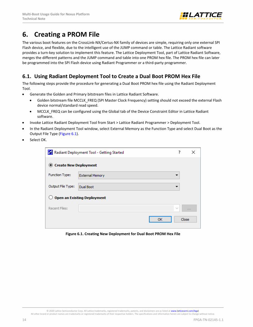
6.1. Using Radiant Deployment Tool to Create a Dual Boot PROM Hex File The following steps provide the procedure for generating a Dual Boot PROM hex file using the Radiant Deployment Tool.
Generate the Golden and Primary bitstream files in Lattice Radiant Software.
Golden bitstream file MCCLK_FREQ (SPI Master Clock Frequency) setting should not exceed the external Flash device normal/standard read speed.
MCCLK_FREQ can be configured using the Global tab of the Device Constraint Editor in Lattice Radiant software.
Invoke Lattice Radiant Deployment Tool from Start > Lattice Radiant Programmer > Deployment Tool.
In the Radiant Deployment Tool window, select External Memory as the Function Type and select Dual Boot as the Output File Type (Figure 6.1).
Select OK.
Figure 6.1. Creating New Deployment for Dual Boot PROM Hex File

Multi-Boot Usage Guide for Nexus Platform Technical Note
© 2020 Lattice Semiconductor Corp. All Lattice trademarks, registered trademarks, patents, and disclaimers are as listed at www.latticesemi.com/legal. All other brand or product names are trademarks or registered trademarks of their respective holders. The specifications and information herein are subject to change without notice.
FPGA-TN-02145-1.1 15
Step 1 of 4: Select Input File(s) window (Figure 6.2)
Click the File Name fields to browse and select the two bitstream files to be used to create the PROM hex file.
The Device Family and Device fields auto populates based on the bitstream files selected.
Select Next.
Figure 6.2. Select Input Files Window

Multi-Boot Usage Guide for Nexus Platform Technical Note
© 2020 Lattice Semiconductor Corp. All Lattice trademarks, registered trademarks, patents, and disclaimers are as listed at www.latticesemi.com/legal. All other brand or product names are trademarks or registered trademarks of their respective holders. The specifications and information herein are subject to change without notice.
16 FPGA-TN-02145-1.1
Step 2 of 4: Dual Boot Options window (Figure 6.3)
Select the Output Format (Intel Hex, Motorola Hex or Extended Tektronix Hex).
Select the SPI Flash Size (4, 8, 16, 32, 64, 128, 256 or 512 Mb).
Select SPI Flash Read Mode (Standard Read, Fast Read, Dual I/O SPI Flash Read or Quad I/O SPI Flash Read).
The Radiant Deployment Tool automatically assigns the bitstream files selected in Step 1 to be used for the Golden pattern and Primary pattern
Change the pattern options by clicking on the drop down menu of the respective fields.
The Starting Address of the Golden pattern is automatically assigned.
Change the Starting Address of the Golden pattern by clicking on the drop down menu.
Select the following options as required.
Byte Wide Bit Mirror – Flips each byte in Intel, Extended Tektronix, or Motorola hexadecimal data files
For example, 0xCD (b1100 1101) will become 0xB3 (b1011 0011) when this is selected
Retain Bitstream Header – By default, Radiant Deployment Tool replaces the bitstream header information (name, version number and date of the file) with 0xFF values.
Selecting this option retains the header information that was generated as the header.
Select Next.
Figure 6.3. Dual Boot Options Window

Multi-Boot Usage Guide for Nexus Platform Technical Note
© 2020 Lattice Semiconductor Corp. All Lattice trademarks, registered trademarks, patents, and disclaimers are as listed at www.latticesemi.com/legal. All other brand or product names are trademarks or registered trademarks of their respective holders. The specifications and information herein are subject to change without notice.
FPGA-TN-02145-1.1 17
Step 3 of 4: Select Output File(s) window (Figure 6.4)
Specify the name of the output PROM hex file in the Output File 1 field.
Select Next.
Figure 6.4. Select Output File Window

Multi-Boot Usage Guide for Nexus Platform Technical Note
© 2020 Lattice Semiconductor Corp. All Lattice trademarks, registered trademarks, patents, and disclaimers are as listed at www.latticesemi.com/legal. All other brand or product names are trademarks or registered trademarks of their respective holders. The specifications and information herein are subject to change without notice.
18 FPGA-TN-02145-1.1
Step 4 of 4: Generate Deployment window (Figure 6.5)
Review the summary information.
If everything is correct, click the Generate button.
The Generate Deployment pane should indicate that the PROM file was generated successfully.
Save the deployment settings by selecting File > Save.
To exit, select File > Exit.
Figure 6.5. Generate Deployment Window

Multi-Boot Usage Guide for Nexus Platform Technical Note
© 2020 Lattice Semiconductor Corp. All Lattice trademarks, registered trademarks, patents, and disclaimers are as listed at www.latticesemi.com/legal. All other brand or product names are trademarks or registered trademarks of their respective holders. The specifications and information herein are subject to change without notice.
FPGA-TN-02145-1.1 19
6.2. Using the Lattice Deployment Tool to Create a Ping-Pong Boot PROM Hex File The following steps provide the procedure for generating a Ping-Pong boot PROM hex file using the Radiant Deployment Tool.
Generate the Primary and Secondary bitstream files in Lattice Radiant software.
When the Primary or Secondary bitstream is the second boot option, it by default becomes the Golden bitstream.
Golden bitstream file MCCLK_FREQ (SPI Master Clock Frequency) setting should not exceed the external Flash device normal/standard read speed.
MCCLK_FREQ can be configured using the Global tab of the Device Constraint Editor in Lattice Radiant software.
Invoke Lattice Radiant Deployment Tool from Start > Lattice Radiant Programmer > Deployment Tool.
In the Radiant Deployment Tool window, select External Memory as the Function Type and select Ping-Pong Boot as the Output File Type (Figure 6.6).
Select OK.
Figure 6.6. Creating New Deployment for Ping-Pong Boot PROM Hex File

Multi-Boot Usage Guide for Nexus Platform Technical Note
© 2020 Lattice Semiconductor Corp. All Lattice trademarks, registered trademarks, patents, and disclaimers are as listed at www.latticesemi.com/legal. All other brand or product names are trademarks or registered trademarks of their respective holders. The specifications and information herein are subject to change without notice.
20 FPGA-TN-02145-1.1
Step 1 of 4: Select Input File(s) window (Figure 6.7)
Click the File Name fields to browse and select the two bitstream files to be used to create the PROM hex file.
The Device Family and Device fields auto populates based on the bitstream files.
Select Next.
Figure 6.7. Select Input Files Window

Multi-Boot Usage Guide for Nexus Platform Technical Note
© 2020 Lattice Semiconductor Corp. All Lattice trademarks, registered trademarks, patents, and disclaimers are as listed at www.latticesemi.com/legal. All other brand or product names are trademarks or registered trademarks of their respective holders. The specifications and information herein are subject to change without notice.
FPGA-TN-02145-1.1 21
Step 2 of 4: Ping-Pong Boot Options window (Figure 6.8)
Select the Output Format (Intel Hex, Motorola Hex, or Extended Tektronix Hex).
Select the SPI Flash Size (4, 8, 16, 32, 64, 128, 256 or 512 Mb).
Select SPI Flash Read Mode (Standard Read, Fast Read, Dual I/O SPI Flash Read or Quad I/O SPI Flash Read).
The Radiant Deployment Tool automatically assigns the bitstream files selected in Step 1 to be used for Primary and Secondary Patterns.
Change the pattern options by clicking on the drop down menu of the respective field.
The Starting Address of the Primary Pattern is automatically assigned and can be modified by clicking on the drop down menu.
The Starting Address of the Secondary Pattern is automatically assigned and can be modified by clicking on the drop down menu.
Select the following options as required.
Generate Jump Table Only – Generates a JUMP table to select an image for booting without changing the physical location of the images in the external SPI Flash.
For example, a JUMP table file can be created to attempt to load Bitstream_2.bit file first. This new JUMP table file can be programmed to the external Flash to overwrite the previous JUMP table file.
Byte Wide Bit Mirror – Flips each byte in Intel, Extended Tektronix or Motorola hexadecimal data files
For example, 0xCD (b1100 1101) becomes 0xB3 (b1011 0011) when this is selected.
Retain Bitstream Header – By default, Radiant Deployment Tool replaces the bitstream header information (name, version number and date of the file) with 0xFF values.
Selecting this option retains the header information that was generated as the header.
Select Next.
Figure 6.8. Ping-Pong Boot Options Window

Multi-Boot Usage Guide for Nexus Platform Technical Note
© 2020 Lattice Semiconductor Corp. All Lattice trademarks, registered trademarks, patents, and disclaimers are as listed at www.latticesemi.com/legal. All other brand or product names are trademarks or registered trademarks of their respective holders. The specifications and information herein are subject to change without notice.
22 FPGA-TN-02145-1.1
Step 3 of 4: Select Output File(s) window (Figure 6.9)
Specify the name of the output PROM hex file in the Output File 1 field.
Select Next.
Figure 6.9. Select Output File Window

Multi-Boot Usage Guide for Nexus Platform Technical Note
© 2020 Lattice Semiconductor Corp. All Lattice trademarks, registered trademarks, patents, and disclaimers are as listed at www.latticesemi.com/legal. All other brand or product names are trademarks or registered trademarks of their respective holders. The specifications and information herein are subject to change without notice.
FPGA-TN-02145-1.1 23
Step 4 of 4: Generate Deployment window (Figure 6.10)
Review the summary information.
If everything is correct, click the Generate button.
The Generate Deployment pane should indicate the PROM file was generated successfully.
Save the deployment settings by selecting File > Save.
To exit, select File > Exit.
Figure 6.10. Generate Deployment Window

Multi-Boot Usage Guide for Nexus Platform Technical Note
© 2020 Lattice Semiconductor Corp. All Lattice trademarks, registered trademarks, patents, and disclaimers are as listed at www.latticesemi.com/legal. All other brand or product names are trademarks or registered trademarks of their respective holders. The specifications and information herein are subject to change without notice.
24 FPGA-TN-02145-1.1
6.3. Using Radiant Deployment Tool to Create a Multi-Boot PROM Hex File The following steps provide the procedure for generating a Multi-Boot PROM hex file using the Radiant Deployment Tool. This procedure is an example for four total bitstreams, Primary Pattern, Golden Pattern, Alternate Pattern 1 and Alternate Pattern 2.
Generate all the bitstream files needed in Lattice Radiant Software.
Golden bitstream file MCCLK_FREQ (SPI Master Clock Frequency) setting should not exceed the external Flash device normal/standard read speed.
MCCLK_FREQ can be configured under the Global tab of the Device Constraint Editor in Lattice Radiant software.
Invoke Lattice Radiant Deployment Tool from Start > Lattice Radiant Programmer > Deployment Tool.
In the Radiant Deployment Tool window, select External Memory as the Function Type and select Advanced SPI Flash as the Output File Type (Figure 6.11).
Select OK.
Figure 6.11. Creating New Deployment for Multi-Boot

Multi-Boot Usage Guide for Nexus Platform Technical Note
© 2020 Lattice Semiconductor Corp. All Lattice trademarks, registered trademarks, patents, and disclaimers are as listed at www.latticesemi.com/legal. All other brand or product names are trademarks or registered trademarks of their respective holders. The specifications and information herein are subject to change without notice.
FPGA-TN-02145-1.1 25
Step 1 of 4: Select Input File(s) window (Figure 6.12)
Click the File Name field to browse and select the primary bitstream file to be used to create the PROM hex file.
The Device Family and Device fields auto populates based on the bitstream files selected.
Select Next.
Figure 6.12. Select Input File Window

Multi-Boot Usage Guide for Nexus Platform Technical Note
© 2020 Lattice Semiconductor Corp. All Lattice trademarks, registered trademarks, patents, and disclaimers are as listed at www.latticesemi.com/legal. All other brand or product names are trademarks or registered trademarks of their respective holders. The specifications and information herein are subject to change without notice.
26 FPGA-TN-02145-1.1
Step 2 of 4: Advanced SPI Flash Options window (Figure 6.13)
Go to the Options tab.
Select the Output Format (Intel Hex, Motorola Hex or Extended Tektronix Hex).
Select the SPI Flash Size (4, 8, 16, 32, 64, 128, 256 or 512 Mb).
Select SPI Flash Read Mode (Standard Read, Fast Read, Dual I/O SPI Flash Read or Quad I/O SPI Flash Read).
Select the following options as required:
Byte Wide Bit Mirror – Flips each byte in Intel, Extended Tektronix, or Motorola hexadecimal data files
For example, 0xCD (b1100 1101) becomes 0xB3 (b1011 0011) when this is selected.
Retain Bitstream Header – By default, Radiant Deployment Tool replaces the bitstream header information (name, version number and date of the file) with 0xFF values. Selecting this option retains the header information that was generated as the header.
Optimize Memory Space – By default, the Radiant Deployment Tool uses the worst case file size for SPI Flash memory space allocation.
a. Worst case size is an uncompressed bitstream with maximum EBR and PCS. This allows maximum flexibility for field upgrades. If a new Primary Pattern file size grows significantly due to less compression or adding EBR blocks, it is guaranteed to fit in the sectors already allocated for Primary Pattern.
b. When this option is selected, the Radiant Deployment Tool uses the actual file size for the address allocation. This reduces wasted SPI Flash space and may allow for a smaller Flash device. If one or more of the new patterns have smaller compression ratio or more EBR/PCS, the new pattern(s) can encroach into another pattern bitstream memory space. If this occurs, the entire SPI Flash needs to be erased/ re-programmed with a new Hex file.
Go to the Multiple Boot tab (Figure 6.14).
Select the Multiple Boot option.
Click on the Golden Pattern browse button to select the Golden Pattern bitstream.
The Starting Address of the Golden Pattern is automatically assigned.
Change the Starting Address of the Golden Pattern by clicking on the drop down menu.
Select the following option as required:
Protect Golden Sector – By default, the golden sector, where the Golden Pattern is stored, is located immediately after the primary sector to save SPI Flash space. When this option is selected, the Golden Pattern location is moved to the first sector in the upper half of the SPI Flash. The new location is reflected in the Golden Patten Starting Address field. This protects the Golden Pattern from accidental erase/reprogram by protecting the upper half of the SPI Flash when it is programmed.
In the Number of Alternate Patterns field, select the number of alternate patterns to include through the drop down menu.
In the Alternate Pattern 1 field, click on the browse button to select the first alternate pattern.
The Starting Address of Alternate Pattern 1 is automatically populated.
You can change the Starting Address of Alternate Pattern 1 by clicking on the drop down menu.
The Next Alternate Pattern to Configure field is automatically populated.
This is the pattern that is loaded during the next PROGRAMN/REFRESH event. You can change the pattern by clicking on the drop down menu.
In the Alternate Pattern 2 field, click on the browse button to select the second alternate pattern.
The Starting Address of Alternate Pattern 2 is automatically populated.
You can change the Starting Address of Alternate Pattern 2 by clicking on the drop down menu.
The Next Alternate Pattern to Configure field is automatically populated.
This is the pattern that is loaded during the next PROGRAMN/REFRESH event. You can change the pattern by clicking on the drop down menu.

Multi-Boot Usage Guide for Nexus Platform Technical Note
© 2020 Lattice Semiconductor Corp. All Lattice trademarks, registered trademarks, patents, and disclaimers are as listed at www.latticesemi.com/legal. All other brand or product names are trademarks or registered trademarks of their respective holders. The specifications and information herein are subject to change without notice.
FPGA-TN-02145-1.1 27
Select Next.
Figure 6.13. Advanced SPI Flash Options – Options Tab Window

Multi-Boot Usage Guide for Nexus Platform Technical Note
© 2020 Lattice Semiconductor Corp. All Lattice trademarks, registered trademarks, patents, and disclaimers are as listed at www.latticesemi.com/legal. All other brand or product names are trademarks or registered trademarks of their respective holders. The specifications and information herein are subject to change without notice.
28 FPGA-TN-02145-1.1
Figure 6.14. Advanced SPI Flash Options – Multiple Boot Tab Window

Multi-Boot Usage Guide for Nexus Platform Technical Note
© 2020 Lattice Semiconductor Corp. All Lattice trademarks, registered trademarks, patents, and disclaimers are as listed at www.latticesemi.com/legal. All other brand or product names are trademarks or registered trademarks of their respective holders. The specifications and information herein are subject to change without notice.
FPGA-TN-02145-1.1 29
Step 3 of 4: Select Output File(s) window (Figure 6.15)
Specify the name of the output PROM hex file in the Output File 1 field.
Select Next.
Figure 6.15. Select Output File Window

Multi-Boot Usage Guide for Nexus Platform Technical Note
© 2020 Lattice Semiconductor Corp. All Lattice trademarks, registered trademarks, patents, and disclaimers are as listed at www.latticesemi.com/legal. All other brand or product names are trademarks or registered trademarks of their respective holders. The specifications and information herein are subject to change without notice.
30 FPGA-TN-02145-1.1
Step 4 of 4: Generate Deployment window (Figure 6.16)
Review the summary information.
If everything is correct, click the Generate button.
The Generate Deployment pane should indicate the PROM file was generated successfully.
Save the deployment settings by selecting File > Save.
To exit, select File > Exit.
Figure 6.16. Generate Deployment Window

Multi-Boot Usage Guide for Nexus Platform Technical Note
© 2020 Lattice Semiconductor Corp. All Lattice trademarks, registered trademarks, patents, and disclaimers are as listed at www.latticesemi.com/legal. All other brand or product names are trademarks or registered trademarks of their respective holders. The specifications and information herein are subject to change without notice.
FPGA-TN-02145-1.1 31
7. Programming the Dual Boot, Ping-Pong Boot, or Multi-Boot Pattern into the SPI Flash Device
The following procedure is for Programming a Dual Boot, Ping-Pong Boot, or Multi-Boot Pattern into the SPI Flash Device using Radiant Programmer:
1. Connect power to the board and connect a download cable from the board to the PC.
2. Invoke Radiant Programmer using one of the following methods:
In Radiant Software window, select Tools > Programmer;
In Radiant Software window, select the Programmer icon ( ) in the Radiant toolbar;
In the Windows Start menu, select Start > Lattice Radiant Programmer > Radiant Programmer;
In the Windows Start menu, select Start > Lattice Radiant Software > Radiant Programmer.
3. Radiant Programmer – Getting Started window opens (Figure 7.1).
Select Create a New Project from a Scan, or Create a new blank project, or Select Open an existing Programmer project.
Select Detect Cable to scan the PC to determine what cable is connected. Or, manually select the type of Cable and Port.
Select OK.
4. Select the Operation field by moving the cursor over it and double clicking the left mouse button.
5. The Device Properties window opens (Figure 7.2).
For Target Memory, select External SPI Flash Memory (SPI Flash).
For Port Interface, select JTAG2SPI.
CrossLink-NX/Certus-NX and Radiant Programmer automatically takes care of the details to connect the JTAG port pins to the SPI interface pins and to program the external SPI Flash device via the JTAG port.
For Access Mode, select Direct Programming.
For Operation, select Erase, Program, Verify.
For Programming File, browse to select the .mcs file.
In the SPI Flash Options field, specify the Family, Vendor, Device, and Package of the Flash device used on the board.
For Data File Size (Bytes), click on the Load from File button.
Select the OK button.
6. Program the external Flash device with one of the following methods:
In the Radiant Programmer window, select Run > Program Device.
In the Radiant Programmer window, select the Program Device icon ( ) in the toolbar.

Multi-Boot Usage Guide for Nexus Platform Technical Note
© 2020 Lattice Semiconductor Corp. All Lattice trademarks, registered trademarks, patents, and disclaimers are as listed at www.latticesemi.com/legal. All other brand or product names are trademarks or registered trademarks of their respective holders. The specifications and information herein are subject to change without notice.
32 FPGA-TN-02145-1.1
Figure 7.1. Radiant Programmer – Getting Started Window

Multi-Boot Usage Guide for Nexus Platform Technical Note
© 2020 Lattice Semiconductor Corp. All Lattice trademarks, registered trademarks, patents, and disclaimers are as listed at www.latticesemi.com/legal. All other brand or product names are trademarks or registered trademarks of their respective holders. The specifications and information herein are subject to change without notice.
FPGA-TN-02145-1.1 33
Figure 7.2. Radiant Programmer – Device Properties Window

Multi-Boot Usage Guide for Nexus Platform Technical Note
© 2020 Lattice Semiconductor Corp. All Lattice trademarks, registered trademarks, patents, and disclaimers are as listed at www.latticesemi.com/legal. All other brand or product names are trademarks or registered trademarks of their respective holders. The specifications and information herein are subject to change without notice.
34 FPGA-TN-02145-1.1
Technical Support Assistance Submit a technical support case through www.latticesemi.com/techsupport.

Multi-Boot Usage Guide for Nexus Platform Technical Note
© 2020 Lattice Semiconductor Corp. All Lattice trademarks, registered trademarks, patents, and disclaimers are as listed at www.latticesemi.com/legal. All other brand or product names are trademarks or registered trademarks of their respective holders. The specifications and information herein are subject to change without notice.
FPGA-TN-02145-1.1 35
Revision History
Revision 1.1, May 2020
Section Change Summary
All Changed the document title to “Multi-Boot Usage Guide for Nexus Platform”.
Introduction
Added support for the Nexus platform including Certus-NX and CrossLink-NX device families.
Resources
CrossLink-NX/Certus-NX Dual Boot Mode
CrossLink-NX/Certus-NX Ping-Pong Boot Mode
CrossLink-NX/Certus-NX Multi-Boot Mode
Creating a PROM FileProgramming the Dual Boot, Ping-Pong Boot, or Multi-Boot Pattern into the SPI Flash Device
Resources Added resources details for Certus-NX device family in Table 2.1, Table 2.2, and Table 2.3.
Revision 1.0, January 2020
Section Change Summary
All Initial release.