MT6582 HSPA + smart phone application processor technical brief
51
MT6582 HSPA+ Smartphone Application Processor Technical Brief Version: 1.0 Release date: 2013-06-14 © 2013 MediaTek Inc. This document contains information that is proprietary to MediaTek Inc. Unauthorized reproduction or disclosure of this information in whole or in part is strictly prohibited. Specifications are subject to change without notice. Free Datasheet http://www.nDatasheet.com
-
Upload
sbsridhar5624 -
Category
Documents
-
view
36 -
download
10
description
smartphone processor technical brief
Transcript of MT6582 HSPA + smart phone application processor technical brief
[email protected],time=2013-08-10 09:29:21,ip=112.90.37.152,doctitle=MT6582WG_Technical_Brief_v1.1.docx,company=Hexing_WCX
MT6582
HSPA+ Smartphone
Application Processor
Technical Brief
Version: 1.0
Release date: 2013-06-14
© 2013 MediaTek Inc.
This document contains information that is proprietary to MediaTek Inc.
Unauthorized reproduction or disclosure of this information in whole or in part is strictly prohibited.
Specifications are subject to change without notice.
Free Datasheet http://www.nDatasheet.com
[email protected],time=2013-08-10 09:29:21,ip=112.90.37.152,doctitle=MT6582WG_Technical_Brief_v1.1.docx,company=Hexing_WCX
MT6582
HSPA+ Smartphone Application Processor
Technical Brief
Confidential A
MediaTek Confidential © 2013 MediaTek Inc. Page 2 of 51
This document contains information that is proprietary to MediaTek Inc.
Unauthorized reproduction or disclosure of this information in whole or in part is strictly prohibited.
Document Revision History
Revision Date Author Description
0.1 2013-03-25 Ray Tzeng First created by Ray Tzeng
1.0 2013-06-14 Ray Tzeng Formal release
1.1 2013-07-11 Ray Tzeng Update video feature
Free Datasheet http://www.nDatasheet.com
[email protected],time=2013-08-10 09:29:21,ip=112.90.37.152,doctitle=MT6582WG_Technical_Brief_v1.1.docx,company=Hexing_WCX
MT6582
HSPA+ Smartphone Application Processor
Technical Brief
Confidential A
MediaTek Confidential © 2013 MediaTek Inc. Page 3 of 51
This document contains information that is proprietary to MediaTek Inc.
Unauthorized reproduction or disclosure of this information in whole or in part is strictly prohibited.
Table of Contents
Document Revision History .................................................................................................................. 2
Table of Contents ................................................................................................................................... 3
1 System Overview .......................................................................................................................... 5
1.1 Platform Features ................................................................................................................. 6 1.2 MODEM Features ................................................................................................................. 7 1.3 Multimedia Features ............................................................................................................. 7 1.4 BT/WLAN/GPS/FM with MT6627 Features .......................................................................... 9 1.5 General Descriptions .......................................................................................................... 10
2 Product Description ................................................................................................................... 12
2.1 Pin Description.................................................................................................................... 12 2.1.1 Ball Map View ..................................................................................................... 12 2.1.1 Pin Coordinate .................................................................................................... 13 2.1.2 Detailed Pin Description ..................................................................................... 22
2.2 Electrical Characteristic ...................................................................................................... 30 2.2.1 Absolute Maximum Ratings ............................................................................... 30 2.2.2 Recommended Operating Conditions ................................................................ 31 2.2.3 Storage Condition ............................................................................................... 31 2.2.4 AC Electrical Characteristics and Timing Diagram ............................................ 32
2.3 System Configuration ......................................................................................................... 35 2.3.1 Constant Tie Pins ............................................................................................... 35
2.4 Power-on Sequence ........................................................................................................... 35 2.5 Analog Baseband ............................................................................................................... 36
2.5.1 Introduction ......................................................................................................... 36 2.5.2 Features ............................................................................................................. 37 2.5.3 Block Diagram .................................................................................................... 37
2.6 Package Information ........................................................................................................... 50 2.6.1 Package Outlines ............................................................................................... 50 2.6.2 Thermal Operating Specifications ...................................................................... 50 2.6.3 Lead-free Packaging .......................................................................................... 50
2.7 Ordering Information ........................................................................................................... 51 2.7.1 Top Marking Definition ....................................................................................... 51
List of Figures Figure 1-1. Block diagram of MT6582 ................................................................................................... 11 Figure 2-1. LPDDR2 ball map view of MT6582 .................................................................................... 12 Figure 2-2. LPDDR3 ball map view of MT6582 .................................................................................... 13 Figure 2-3. Basic timing parameter for LPDDR2 commands ................................................................ 32
Free Datasheet http://www.nDatasheet.com
[email protected],time=2013-08-10 09:29:21,ip=112.90.37.152,doctitle=MT6582WG_Technical_Brief_v1.1.docx,company=Hexing_WCX
MT6582
HSPA+ Smartphone Application Processor
Technical Brief
Confidential A
MediaTek Confidential © 2013 MediaTek Inc. Page 4 of 51
This document contains information that is proprietary to MediaTek Inc.
Unauthorized reproduction or disclosure of this information in whole or in part is strictly prohibited.
Figure 2-4. Basic timing parameter for LPDDR2 write .......................................................................... 33 Figure 2-5. Basic timing parameter for LPDDR2 read .......................................................................... 33 Figure 2-6. Power on/off sequence with and without XTAL .................................................................. 35 Figure 2-7. Block diagram of BBRX-ADC ............................................................................................. 37 Figure 2-8. Block diagram of BBTX-DAC .............................................................................................. 39 Figure 2-9. Block diagram of APC-DAC ................................................................................................ 40 Figure 2-10. Block diagram of VBIAS-DAC .......................................................................................... 41 Figure 2-11. Block diagram of AUXADC ............................................................................................... 42 Figure 2-12. Block diagram of PLL ....................................................................................................... 45 Figure 2-13. Outlines and dimensions of FCCSP 10.6mm*11.0mm, 475-ball, 0.4mm pitch package . 50 Figure 2-14. Top mark of MT6582 ......................................................................................................... 51
List of Tables Table 2-1. LPDDR2 pin coordinate ....................................................................................................... 13 Table 2-2. LPDDR3 pin coordinate ....................................................................................................... 18 Table 2-3. Acronym for pin type ............................................................................................................ 22 Table 2-4. Detailed pin description ........................................................................................................ 22 Table 2-5. Absolute maximum ratings for power supply ....................................................................... 30 Table 2-6. Recommended operating conditions for power supply ........................................................ 31 Table 2-7. LPDDR2 AC timing parameter table of external memory interfaces .................................... 33 Table 2-8. Constant tied pins of MT6582 .............................................................................................. 35 Table 2-9. Baseband downlink specifications ....................................................................................... 37 Table 2-10. Baseband uplink transmitter specifications ........................................................................ 39 Table 2-11. APC-DAC specifications ..................................................................................................... 40 Table 2-12. VBIAS-DAC specifications ................................................................................................. 41 Table 2-13. Definitions of AUXADC channels ....................................................................................... 42 Table 2-14. AUXADC specifications ...................................................................................................... 43 Table 2-15. Clock squarer specifications .............................................................................................. 43 Table 2-16. ARMPLL specifications ....................................................................................................... 45 Table 2-17. MAINPLL specifications ..................................................................................................... 46 Table 2-18. MMPLL specifications ........................................................................................................ 46 Table 2-19. UNIVPLL specifications ...................................................................................................... 46 Table 2-20. MSDCPLL specifications .................................................................................................... 47 Table 2-21. MDPLL1 specifications ....................................................................................................... 47 Table 2-22. WPLL specifications ........................................................................................................... 47 Table 2-23. WHPLL specifications ........................................................................................................ 48 Table 2-24. MCUPLL specifications ...................................................................................................... 48 Table 2-25. VENCPLL specifications .................................................................................................... 48 Table 2-26. Temperature sensor specifications ..................................................................................... 49 Table 2-27. Thermal operating specifications ....................................................................................... 50
Free Datasheet http://www.nDatasheet.com
[email protected],time=2013-08-10 09:29:21,ip=112.90.37.152,doctitle=MT6582WG_Technical_Brief_v1.1.docx,company=Hexing_WCX
MT6582
HSPA+ Smartphone Application Processor
Technical Brief
Confidential A
MediaTek Confidential © 2013 MediaTek Inc. Page 5 of 51
This document contains information that is proprietary to MediaTek Inc.
Unauthorized reproduction or disclosure of this information in whole or in part is strictly prohibited.
1 System Overview
MT6582 is a highly integrated baseband platform incorporating modem, application processing and
connectivity subsystems to enable 3G smart phone applications. The chip integrates a Quad-core
ARM® Cortex-A7 MPCoreTM
operating up to 1.3GHz, an ARM® Cortex-R4 MCU and a powerful multi-
standard video accelerator. The MT6582 interfaces to NAND flash memory, LPDDR2 and LPDDR3 for
optimal performance and also supports booting from SLC NAND or eMMC to minimize the overall
BOM cost. In addition, an extensive set of interfaces are included to interface to cameras, touch-
screen displays, and MMC/SD cards.
The application processor, a Quad-core ARM® Cortex-A7 MPCoreTM
which includes a NEON
multimedia processing engine, offers processing power necessary to support the latest OpenOS
along with its demanding applications such as web browsing, email, GPS navigation and games. All
are viewed on a high resolution touch screen display with graphics enhanced by the 3D graphics
acceleration. The multi-standard video accelerator and an advanced audio subsystem are also
included to provide advanced multimedia applications and services such as streaming audio and
video, a multitude of decoders and encoders such as H.264 and MPEG-4. Audio supports include FR,
HR, EFR, AMR FR, AMR HR and Wide-Band AMR vocoders, polyphonic ringtones and advanced
audio functions such as echo cancellation, hands-free speakerphone operation and noise cancellation.
An ARM® Cortex-R4, DSP, and 2G and 3G coprocessors provide a powerful modem subsystem
capable of supporting Category 14 (21 Mbps) HSDPA downlink and Category 6 (5.76 Mbps) HSUPA
uplink data rates as well as Class 12 GPRS, EDGE.
MT6582 includes four wireless connectivity functions, WLAN, Bluetooth, GPS, and FM receiver. The
RF parts of those four blocks are put in the MT6627 chip. With four advanced radio technologies
integrated into one single chip, MT6582/MT6627 provides the best and most convenient connectivity
solution among the industry. MT6582/MT6627 implements advanced and sophisticated Radio
Coexistence algorithms and hardware mechanisms. It also supports single antenna sharing among
2.4 GHz antenna for Bluetooth, WLAN and 1.575 GHz for GPS. The enhanced overall quality is
achieved for simultaneous voice, data, and audio/video transmission on mobile phones and Media
Tablets. The small footprint with low-power consumption greatly reduces the PCB layout resource.
Free Datasheet http://www.nDatasheet.com
[email protected],time=2013-08-10 09:29:21,ip=112.90.37.152,doctitle=MT6582WG_Technical_Brief_v1.1.docx,company=Hexing_WCX
MT6582
HSPA+ Smartphone Application Processor
Technical Brief
Confidential A
MediaTek Confidential © 2013 MediaTek Inc. Page 6 of 51
This document contains information that is proprietary to MediaTek Inc.
Unauthorized reproduction or disclosure of this information in whole or in part is strictly prohibited.
1.1 Platform Features
General
Smartphone two MCU subsystems
architecture
SLC NAND flash and eMMC bootloader
AP MCU subsystem
Quad-core ARM® Cortex-A7 MPCoreTM
operating at 1.3 GHz
NEON multimedia processing engine
with SIMDv2 / VFPv4 ISA support
32KB L1 I-cache and 32KB L1 D-cache
512KB unified L2 cache
DVFS technology with adaptive
operating voltage from 1.05V to 1.26V
MD MCU subsystem
ARM® Cortex-R4 processor with
maximum 491.5 MHz operation
frequency
32KB I-cache, 16KB D-cache
256KB TCM (tightly-coupled memory)
DSP for running modem/voice tasks,
with maximum 240MHz operation
frequency
High-performance AXI and AHB bus
General DMA engine and dedicated
DMA channels for peripheral data
transfer
Watchdog timer for system error
recovery
Power management for clock gating
control
CONN MCU subsystem
Andes N9 processor with 32KB I-cache,
16KB D-cache
MD external interfaces
Dual SIM/USIM interface supported
Interface pins with RF and radio-related
peripherals (antenna tuner, PA, …)
External memory interface
Supports LPDDR2/3 up to 2GB
32-bit data bus width
Memory clock up to 533 MHz
Supports self-refresh/partial self-refresh
mode
Low-power operation
Programmable slew rate for memory
controller’s IO pads
Supports dual rank memory device
Advanced bandwidth arbitration control
Security
ARM® TrustZone® Security
Connectivity
USB2.0 high-speed dual mode
supporting 8 Tx and 8 Rx endpoints
NAND flash controller supporting NAND
bootable, iNAND2® and MoviNAND®
4 UARTs for external devices and
debugging interfaces
SPI master for external devices
3 I2C to control peripheral devices, e.g.
CMOS image sensor, or LCM module
I2S master output and master/slave
input for connection with optional
external hi-end audio codec
GPIOs
3 sets of memory card controller
supporting SD/SDHC/MS/MSPRO/MMC
and SDIO2.0/3.0 protocols
Operating conditions
Core voltage: 1.15V
Free Datasheet http://www.nDatasheet.com
[email protected],time=2013-08-10 09:29:21,ip=112.90.37.152,doctitle=MT6582WG_Technical_Brief_v1.1.docx,company=Hexing_WCX
MT6582
HSPA+ Smartphone Application Processor
Technical Brief
Confidential A
MediaTek Confidential © 2013 MediaTek Inc. Page 7 of 51
This document contains information that is proprietary to MediaTek Inc.
Unauthorized reproduction or disclosure of this information in whole or in part is strictly prohibited.
Processor DVFS+SRAM voltage :
1.05V~1.26V (Typ. 1.15V ; sleep mode
0.85V)
I/O voltage: 1.8V/2.8V/3.3V
Memory: 1.2V
NAND: 1.8V/2.8V
LCM interface: 1.8V
Clock source: 26-MHz, 32.768-kHz
Package
Type: FCCSP
10.6mm x 11mm
Height: 1.0mm maximum
Ball count: 475 balls
Ball pitch: 0.4mm
1.2 MODEM Features
3G UMTS FDD supported features (with
MT6166)
3G modem supports most main features
in 3GPP Release 7 and Release 8
CPC (DTX in CELL_DCH, UL DRX DL
DRX), HS-SCCH-less, HS-DSCH
Dual cell operation
MAC-ehs
Two DRX (receiver diversity) schemes
in URA_PCH and CELL_PCH
Uplink Cat. 6, throughput up to 5.7Mbps
Downlink Cat. 14, throughput up to
21Mbps
Fast dormancy
ETWS
Network selection enhancements
Radio interface and baseband front-end
High dynamic range delta-sigma ADC
converts the downlink analog I and Q
signals to digital baseband
10-bit D/A converter for Automatic
Power Control (APC)
Programmable radio Rx filter with
adaptive gain control
Dedicated Rx filter for FB acquisition
Baseband Parallel Interface (BPI) with
programmable driving strength (shared
by 2G & 3G modem)
Supports multi-band
GSM modem and voice CODEC
Dial tone generation
Noise reduction
Echo suppression
Advanced sidetone oscillation reduction
Digital sidetone generator with
programmable gain
Two programmable acoustic
compensation filters
GSM quad vocoders for adaptive
multirate (AMR), enhanced full rate
(EFR), full rate (FR) and half rate (HR)
GSM channel coding, equalization and
A5/1, A5/2 and A5/3 ciphering
GPRS GEA1, GEA2 and GEA3
ciphering
Programmable GSM/GPRS/EDGE
modem
Packet switched data with
CS1/CS2/CS3/CS4 coding schemes
GSM circuit switch data
GPRS/EDGE Class 12
Supports SAIC (single antenna
interference cancellation) technology
Supports VAMOS (Voice services over
Adaptive Multi-user channels on One
Slot) technology in R9 spec
1.3 Multimedia Features
Display
Supports portrait panel resolution up to
HD (1280x720)
MIPI DSI interface (4 data lanes)
Free Datasheet http://www.nDatasheet.com
[email protected],time=2013-08-10 09:29:21,ip=112.90.37.152,doctitle=MT6582WG_Technical_Brief_v1.1.docx,company=Hexing_WCX
MT6582
HSPA+ Smartphone Application Processor
Technical Brief
Confidential A
MediaTek Confidential © 2013 MediaTek Inc. Page 8 of 51
This document contains information that is proprietary to MediaTek Inc.
Unauthorized reproduction or disclosure of this information in whole or in part is strictly prohibited.
Embedded LCD gamma correction
Supports true colors
4 overlay layers with per-pixel alpha
channel and gamma table
Supports spatial and temporal dithering
Supports side-by-side format output to
stereo 3D panel in both portrait and
landscape modes
Supports color enhancement
Supports adaptive contrast
enhancement
Supports image/video/graphic
sharpness enhancement
Supports dynamic backlight scaling
Graphics
OpenGL ES 1.1/2.0 3D graphic
accelerator capable of processing
53.25M tri/sec and 1000M pixel/sec @
500MHz
OpenVG1.1 vector graphics accelerator
Image
Integrated image signal processor
supports 8 MP
Supports electronic image stabilization
Supports video stabilization
Supports preference color adjustment
Supports noise reduction
Supports lens shading correction
Supports auto sensor defect pixel
correction
Supports AE/AWB/AF
Supports edge enhancement
(sharpness)
Supports face detection and visual
tracking
Supports zero shutter delay image
capture
Supports capturing full size image when
recording video (up to 8M sensor)
Supports MIPI CSI-2 high-speed
camera serial interface with 4 data lane
(for main) + 2 data lane (for sub)
Hardware JPEG encoder: Baseline
encoding with 120M pixel/sec
Supports YUV422/YUV420 color format
and EXIF/JFIF format
Video
H.264 decoder: Baseline 1080p @
30fps/40Mbps
H.264 decoder: Main/high profile
1080p@30fps/40Mbps
Sorenson H.263/H.263 decoder: 1080p
@ 30fps/40Mbps
MPEG-4 SP/ASP decoder: 1080p @
30fps/40Mbps
DIVX4/DIVX5/DIVX6/DIVX HD/XVID
decoder: 1080p @ 30fps/40Mbps
VP8 decoder: 1080p @ 30fps/6Mbps
(SW)
VC-1 decoder: 1080p @ 30fps/20Mbps
(SW)
MPEG-4 encoder: Simple profile D1 @
30fps (SW)
H.263 encoder: D1 @ 30fps (SW)
H.264 encoder: High profile 1080p @
30fps
Audio
Sampling rates supported: 8kHz to
48kHz
Sample formats supported: 8-bit/16-bit,
Mono/Stereo
Interfaces supported: DAI, I2S, PCM
4-band IIR compensation filter to
enhance loudspeaker responses
Proprietary audio post-processing
technologies: BesLoudness, Android
built-in post processing
Audio encode: AMR-NB, AMR-WB,
AAC, OGG, ADPCM
Free Datasheet http://www.nDatasheet.com
[email protected],time=2013-08-10 09:29:21,ip=112.90.37.152,doctitle=MT6582WG_Technical_Brief_v1.1.docx,company=Hexing_WCX
MT6582
HSPA+ Smartphone Application Processor
Technical Brief
Confidential A
MediaTek Confidential © 2013 MediaTek Inc. Page 9 of 51
This document contains information that is proprietary to MediaTek Inc.
Unauthorized reproduction or disclosure of this information in whole or in part is strictly prohibited.
Audio decode: WAV, MP3, MP2,
AAC, AMR-NB, AMR-WB, MIDI,
Vorbis, APE, AAC-plus v1, AAC-plus
v2, FLAC, WMA, ADPCM
Speech
Speech codec (FR, HR, EFR, AMR FR,
AMR HR and Wide-Band AMR)
CTM
Noise reduction
Noise suppression
Noise cancellation
Dual-MIC noise cancellation
Echo cancellation
Echo suppression
Dual-MIC input
Digital MIC input
1.4 BT/WLAN/GPS/FM with
MT6627 Features
Common
Self calibration
Single TCXO and TSX for GPS, BT
and WLAN
Best-in-class current consumption
performance
OS supported: Android
Intelligent BT/WLAN coexistence
scheme
Single antenna support for
WLAN/Bluetooth/GPS
WLAN
Single-band (2.4GHz) single stream
802.11 b/g/n MAC/BB/RF
802.11 d/h/k compliant
Security: WFA WPA/WPA2 personal,
WPS2.0, WAPI (hardware)
QoS: WFA WMM, WMM PS
Supports 802.11n optional features:
STBC, A-MPDU, Blk-Ack, RIFS, MCS
Feedback, 20/40MHz coexistence
(PCO), unscheduled PSMP
Supports 802.11w Protected Managed
Frames
Supports WiFi Direct (WFA P-2-P
standard) and Wi-Fi Miracast (Wi-Fi
Display)
Supports Wi-Fi HotSpot 2.0
Integrated PA with max 21dBm output
power
Typical -77.5 dBm 2.4GHz receiver
sensitivity at 11g 54Mbps mode
Per packet TX power control
Bluetooth
Bluetooth specification v2.1+EDR
Bluetooth specification 3.0+HS
compliance
Bluetooth v4.0 Low Energy (LE)
Integrated PA with 10dBm (class 1)
transmit power and Balun
Rx sensitivity: GFSK -95dBm, DQPSK
-94dBm, 8-DPSK -88dBm
Best-in-class BT/Wi-Fi coexistence
performance
Up to 4 piconets simultaneously with
background inquiry/page scan
Supports Scatternet
Packet loss concealment (PLC)
function for better voice quality
Low-power scan function to reduce the
power consumption in scan modes
GPS
Supports GPS/QZSS/SBAS
(WAAS/MSAS/EGNOS/GAGAN)
Best-in-class sensitivity performance
-165 dBm tracking sensitivity
-163 dBm hot start sensitivity
-148 dBm cold start sensitivity
Free Datasheet http://www.nDatasheet.com
[email protected],time=2013-08-10 09:29:21,ip=112.90.37.152,doctitle=MT6582WG_Technical_Brief_v1.1.docx,company=Hexing_WCX
MT6582
HSPA+ Smartphone Application Processor
Technical Brief
Confidential A
MediaTek Confidential © 2013 MediaTek Inc. Page 10 of 51
This document contains information that is proprietary to MediaTek Inc.
Unauthorized reproduction or disclosure of this information in whole or in part is strictly prohibited.
-151 dBm warm start
sensitivity
AGPS sensitivity is 6dB design margin
over 3GPP
Full A-GPS capability
(E911/SUPL/EPO/HotStill)
Active interference cancellation for up
to 8 in-band tones
Supports TCXO
Supports co-clock with AP/MD
5Hz update rate
FM
76-108MHz with 50kHz step
Supports RDS/RBDS
Digital stereo modulator/demodulator
Simplified digital audio interface (I2S)
Fast seek time 30ms/channel
Stereo noise reduction
Audio sensitivity 2dBµVemf
((S+N)/N=26dB)
Audio S/N 60dB
Anti-jamming
Integrated short antenna
WBT IPD
Integrated matching network, balance
band-pass filter, GPS-WBT diplexer.
Fully integrated in one IPD die
Supports single and dual antenna
operation.
GPS IPD
Integrated high-pass type matching
network and 5th-order ellipse low-pass
filter.
Fully integrated in one IPD die
Supports single and dual antenna
operation.
1.5 General Descriptions
MediaTek MT6582 is a highly integrated 3G System-on-chip (SoC) which incorporates advanced
features e.g. HSPA R8 modem, Quad-core ARM® Cortex-A7 MPCoreTM
operating at 1.3GHz, 3D
graphics (OpenGL|ES 2.0), 8M camera ISP, LPDDR2/3 533 MHz and high-definition 1080p video
decoder. MT6582 helps phone manufacturers build high-performance 3G smart phones with PC-like
browser, 3D gaming and cinema class home entertainment experiences.
World-leading technology
Based on MediaTek’s world-leading mobile chip SoC architecture with advanced 28nm process,
MT6582 is the brand-new generation smart phone SoC integrating MediaTek HSPA R8 modem,
1.3GHz Quad-core ARM® Cortex-A7 MPCoreTM
, 3D graphics and high-definition 1080p video
decoder.
Rich in features, high-valued product
To enrich the camera features, MT6582 equips a 8M camera ISP with advanced features e.g. auto
focus, anti-handshake, auto sensor defect pixel correction, continuous video AF, face detection, burst
shot, optical zoom, panorama view and 3D photos.
Incredible browser experience
Free Datasheet http://www.nDatasheet.com
[email protected],time=2013-08-10 09:29:21,ip=112.90.37.152,doctitle=MT6582WG_Technical_Brief_v1.1.docx,company=Hexing_WCX
MT6582
HSPA+ Smartphone Application Processor
Technical Brief
Confidential A
MediaTek Confidential © 2013 MediaTek Inc. Page 11 of 51
This document contains information that is proprietary to MediaTek Inc.
Unauthorized reproduction or disclosure of this information in whole or in part is strictly prohibited.
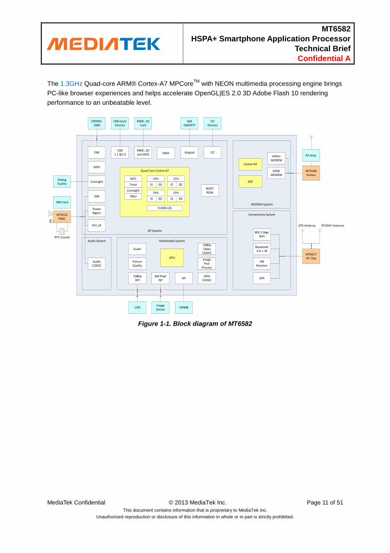
The 1.3GHz Quad-core ARM® Cortex-A7 MPCoreTM
with NEON multimedia processing engine brings
PC-like browser experiences and helps accelerate OpenGL|ES 2.0 3D Adobe Flash 10 rendering
performance to an unbeatable level.
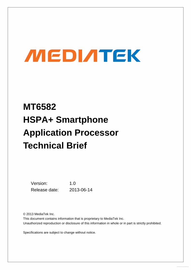
Figure 1-1. Block diagram of MT6582
AP System
EMI
LPDDR2-1066
32
-bit
USB 1.1 &2.0
Keypad I2C
GPIO
SIM
BOOT ROM
MMC, SD and SDIO
USB Host/Devices
8x8 QWERTY
I2C Devices
MMC, SD Card
Quad Core Cortex-A7
CPU
I$ D$
CPU
I$ D$
512KB L2$
CPU
I$ D$
CPU
I$ D$
SPI8M Pixel
ISP1080p
DPI
Picture Quality
Scaler
Image Post
Process
1080p Video
CODEC
GPU
JPEG CODEC
Cortex-R4
HSPA+ MODEM
EDGE MODEM
802.11bgn WiFi
Bluetooth 4.0 + HS
DMA
Timer
INTC
FM Receiver
GPS
MODEM System
Connectivity System
Multimedia System
Coresight
PMU
MT6627 RF Chip
GPS Antenna BT/WiFi Antenna
DSP
Power Mgmt.
MT6323 PMIC
Audio System
Image Sensor
LCM
MT6166Xceiver
RF Amp.
SIM Card
MIP
I CSI
MIP
I DSI
CMMB
RTC I/F
Audio CODEC
CoresightDebug Facility
RTC Crystal
Free Datasheet http://www.nDatasheet.com
[email protected],time=2013-08-10 09:29:21,ip=112.90.37.152,doctitle=MT6582WG_Technical_Brief_v1.1.docx,company=Hexing_WCX
MT6582
HSPA+ Smartphone Application Processor
Technical Brief
Confidential A
MediaTek Confidential © 2013 MediaTek Inc. Page 12 of 51
This document contains information that is proprietary to MediaTek Inc.
Unauthorized reproduction or disclosure of this information in whole or in part is strictly prohibited.
2 Product Description
2.1 Pin Description
2.1.1 Ball Map View
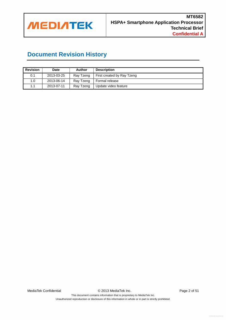
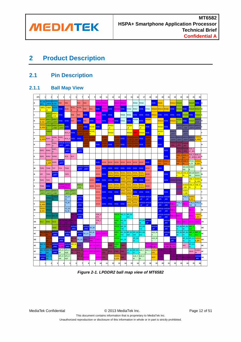
Figure 2-1. LPDDR2 ball map view of MT6582
475 1 2 3 4 5 6 7 8 9 10 11 12 13 14 15 16 17 18 19 20 21 22 23 24 25 26
ATP_ME
MPLL
AVSS18
_MEM
PLL
AVDD1
8_ME
MPLL
RA9 RA6 RA4 RA3 RDQ19 RDQ23 RDQ21 RDQ22 RDQ4 RDQ6 DVSS RDQ9 RDQ12 RDQ25 RDQ29 DVSS A
BCMPCL
K
CMMC
LK
REXTD
NDVSS RCKE
RCS1_
B
RCS0_
BRA0 RA1 DVSS RDQ16 DVSS RDQ18 DVSS RDQ3 RDQ7 DVSS RDQ5 RDQ10 RDQ14 RDQ8 DVSS RDQ26 DVSS RDQ28 RDQ27 B
CMSDC1
_DAT2
MSDC1
_CLKDVSS RA8 RA5 DVSS RDQ17 DVSS DVSS RDQ0 RDQ2 DVSS DVSS DVSS RDQ11 DVSS DVSS DVSS DVSS RDQ30 DVSS RDQ31 C
DDVDD1
8_IO2
MSDC1
_DAT1
MSDC1
_DAT3DVSS DVSS RA7 DVSS RA2 DVSS
RDQM
2DVSS RDQ20 DVSS RDQ1 DVSS
RDQM
0DVSS
RDQM
1RDQ13 DVSS RDQ15
RDQM
3DVSS RDQ24
MSDC0
_CLKD
EDVDD2
8_MSD
C1
CMDAT
0
MSDC1
_CMD
MSDC1
_DAT0DVSS
DVDD1
2_EMIDVSS RCLK0 DVSS
RDQS2
_B
RDQS0
_B
RDQS1
_BDVSS RDQS3 DVSS
MSDC0
_DAT6
MSDC0
_CMD
MSDC0
_DAT2
MSDC0
_DAT3E
FCMDAT
1RCP_A DVSS
DVDD1
2_EMI
DVDD1
2_EMI
RCLK0_
BRDQS2 RDQS0 VREF RDQS1 DVSS
RDQS3
_B
MSDC0
_DAT7
MSDC0
_DAT5F
GDVDD1
8_MIPII
O
RDP3RDN0_
A
RDP0_
ARCN_A DVSS DVSS
DVDD1
2_EMI
DVDD1
2_EMI
DVDD1
2_EMI
DVDD1
2_EMIDVSS
DVDD1
2_EMI
DVDD1
2_EMIDVSS
DVDD1
2_EMIDVSS
MSDC0
_DAT0
MSDC0
_DAT1
MSDC0
_DAT4
MSDC0
_RSTB
DVDD1
8_MSD
C0
G
H RDN3RDN1_
A
DVSS18
_MIPII
O
DVSS18
_MIPII
O
DVDD1
2_EMIDVSS
DVDD1
2_EMIDVSS
DVDD1
2_EMIDVSS
DVDD1
2_EMI
DVDD1
2_EMIDVSS
DVDD1
2_EMIDVSS
PWRAP
_SPI0_
MO
PWRAP
_SPI0_
CK
PWRAP
_INTH
J RDP2 RDN2RDP1_
A
DVSS18
_MIPII
O
DVSS18
_MIPII
O
DVSSPWRAP
_SPI0_
CSN
PWRAP
_SPI0_
MI
AUD_D
AT_MO
SI
J
K RDP1 RDN1 RDN0 RCN RCP DVSSSIM1_S
IO
SIM2_S
RST
AUD_D
AT_MIS
O
AUD_C
LK_MO
SI
K
LDVDD1
8_MIPI
TX
RDP0DVSS18
_MIPIT
X
DVSS VCCK VCCK VCCK VCCK VCCK VCCK VCCK DVSSSIM2_S
CLK
SIM1_S
CLK
SIM1_S
RST
SIM2_S
IO
RTC32
K_CK
DVDD1
8_IO0L
M TDP0 TDN0 TCP TCN TDN3DVSS18
_MIPIT
X
DVSS18
_MIPIT
X
VCCK DVSS DVSS DVSS DVSS DVSS DVSS DVSS VCCK DVSSSRCLKE
NAI
SYSRST
BM
N VRT TDN1DVSS18
_MIPIT
X
TDP3 VCCK DVSSVCCK_
VPROC
VCCK_
VPROC
VCCK_
VPROC
VCCK_
VPROC
VCCK_
VPROC
VCCK_
VPROCVCCK DVSS
CHD_D
P
CHD_D
M
SRCLKE
NA
WATC
HDOGN
P TDP2 TDP1 VCCK DVSS DVSS DVSS DVSSVCCK_
VPROC
VCCK_
VPROCDVSS DVSS VCCK DVSS URXD2 UTXD2
USB_V
RT
AVDD1
8_USBP
R TDN2 DVSSDVDD1
8_EFUS
E
FSOUR
CE_P
MSDC2
_CLKVCCK VCCK DVSS
VCCK_
VPROC
VCCK_
VPROC
VCCK_
VPROC
VCCK_
VPROC
VCCK_
VPROC
VCCK_
VPROCVCCK URXD3
AVSS33
_USB
USB_D
M
USB_D
PR
TMSDC2
_DAT2
MSDC2
_DAT3
MSDC2
_CMD
MSDC2
_DAT1
MSDC2
_DAT0VCCK DVSS DVSS DVSS
VCCK_
VPROC
VCCK_
VPROCDVSS DVSS DVSS DVSS UTXD3
AVDD3
3_USBT
U UTXD1LCM_R
ST
I2S_LR
CK
AVSS18
_WBGVCCK DVSS DVSS
VCCK_
VPROC
VCCK_
VPROC
AVSS18
_AP
AVSS18
_AP
AVSS18
_MD
AVSS18
_MD
PCM_T
X
DVDD1
8_IO1U
VDVDD2
8_MSD
C2
URXD1I2S_BC
K
AVSS18
_WBGVCCK DVSS DVSS DVSS DVSS
VCCK_
VPROC
VCCK_
VPROC
AVSS18
_AP
AVSS18
_AP
AVSS18
_MD
AVSS18
_MDEINT1
PCM_C
LKEINT3
PCM_S
YNC
PCM_R
XV
WDVDD1
8_IO3URXD0
I2S_DA
TA_IN
AVSS18
_WBG
AVSS18
_MD
AVSS18
_MDEINT0 EINT4 W
Y UTXD0 DSI_TEWB_CR
TL0
AVSS18
_WBG
F2W_D
ATA
KPCOL
2
BSI_CL
K
BPI_BU
S15
AVSS18
_MD
AVSS18
_MDEINT10 EINT9 EINT5
DVDD1
8_IO1Y
AA SCL2 SDA2 SCL0WB_CR
TL3
WB_CR
TL2
WB_CR
TL1
F2W_C
LK
KPRO
W2
BSI_DA
TA1
BPI_BU
S8
AVSS18
_AP
AVSS18
_MDEINT6 EINT2 EINT8 EINT7 AA
AB SDA0WB_CR
TL5
WB_CR
TL4
AVSS18
_WBG
AVSS18
_WBGSPI_MI
KPCOL
0
BSI_DA
TA0
BPI_BU
S13
AVSS18
_AP
AVSS18
_MD
BPI_BU
S1
BPI_BU
S0
ANT_S
EL0AB
ACWB_RX
IP
WB_RX
IN
AVSS18
_WBG
AVSS18
_WBG
AVSS18
_WBGSPI_CS
SPI_M
OEINT20 EINT17
KPRO
W0
BSI_DA
TA2
BPI_BU
S14
BPI_BU
S10
BPI_BU
S12
AUX_IN
0
AVSS18
_MD
BPI_BU
S4
BPI_BU
S3
ANT_S
EL2
ANT_S
EL1AC
ADWB_RX
QP
AVSS18
_WBG
XIN_W
BGSPI_CK SCL1
DISP_P
WMEINT18
KPCOL
1BSI_EN
BPI_BU
S9
AUX_IN
1
AVSS18
_MD
BPI_BU
S6
BPI_BU
S2
DVDD2
8_BPIAD
AEWB_TX
IP
WB_RX
QN
AVSS18
_WBG
AVDD1
8_WBG
AVSS18
_WBG
WB_SE
NSDA1 EINT19 EINT16 JTDO
KPRO
W1TXBPI
DVDD1
8_PLLG
P
AVDD1
8_AP
AVDD1
8_MD
AVDD2
8_DACAPC
BPI_BU
S5AE
AFWB_TX
IN
WB_TX
QN
AVSS18
_WBG
GPS_R
XIP
GPS_R
XQN
WB_RS
TB
WB_SD
ATAEINT14 GPIO13 EINT11
TESTM
ODEJTCK JTMS VM1
BPI_BU
S11
BPI_BU
S7
AUX_Y
P
AUX_X
P
AVSS_R
EFN
UL_Q_
NUL_I_N UL_I_P VBIAS
CLK26
MAF
AGAVSS18
_WBG
WB_TX
QP
GPS_R
XIN
GPS_R
XQP
WB_SC
LKEINT15 GPIO12 JTDI
DVDD1
8_IO4VM0
AUX_Y
M
AUX_X
MREFP
UL_Q_
P
DL_Q_
P
DL_Q_
NDL_I_N DL_I_P
AVSS18
_MDAG
1 2 3 4 5 6 7 8 9 10 11 12 13 14 15 16 17 18 19 20 21 22 23 24 25 26
Free Datasheet http://www.nDatasheet.com
[email protected],time=2013-08-10 09:29:21,ip=112.90.37.152,doctitle=MT6582WG_Technical_Brief_v1.1.docx,company=Hexing_WCX
MT6582
HSPA+ Smartphone Application Processor
Technical Brief
Confidential A
MediaTek Confidential © 2013 MediaTek Inc. Page 13 of 51
This document contains information that is proprietary to MediaTek Inc.
Unauthorized reproduction or disclosure of this information in whole or in part is strictly prohibited.
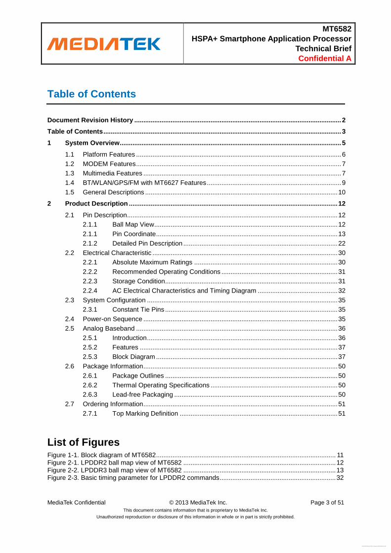
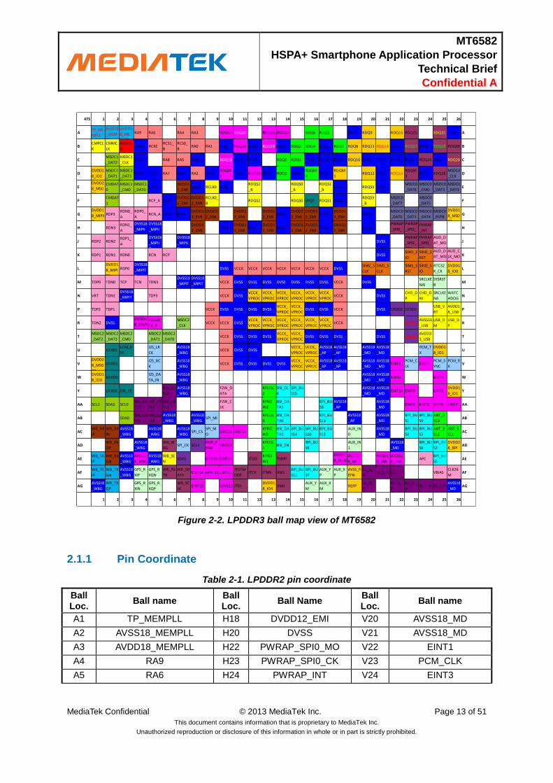
Figure 2-2. LPDDR3 ball map view of MT6582
2.1.1 Pin Coordinate
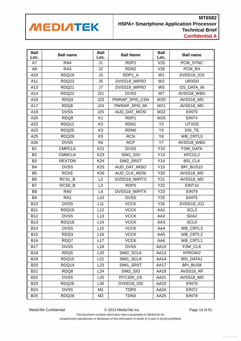
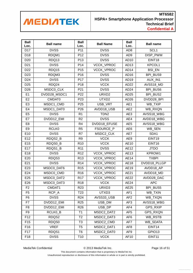
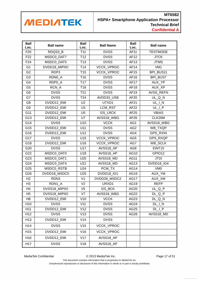
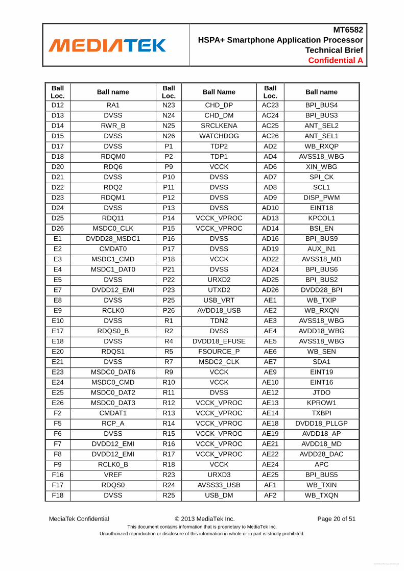
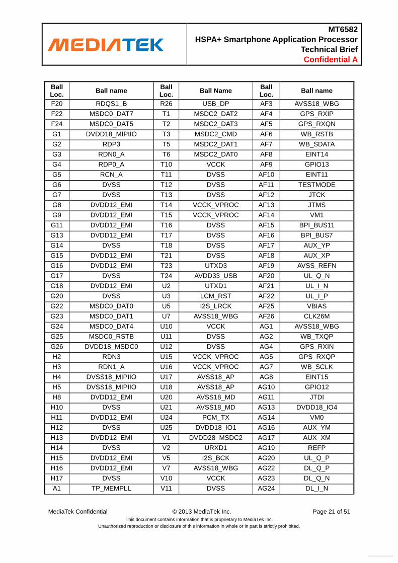
Table 2-1. LPDDR2 pin coordinate
Ball Loc.
Ball name Ball Loc.
Ball Name Ball Loc.
Ball name
A1 TP_MEMPLL H18 DVDD12_EMI V20 AVSS18_MD
A2 AVSS18_MEMPLL H20 DVSS V21 AVSS18_MD
A3 AVDD18_MEMPLL H22 PWRAP_SPI0_MO V22 EINT1
A4 RA9 H23 PWRAP_SPI0_CK V23 PCM_CLK
A5 RA6 H24 PWRAP_INT V24 EINT3
475 1 2 3 4 5 6 7 8 9 10 11 12 13 14 15 16 17 18 19 20 21 22 23 24 25 26
ATP_ME
MPLL
AVSS18
_MEM
PLL
AVDD1
8_ME
MPLL
RA9 RA6 RA4 RA3 RDQ17 RDQ20 RDQ23 RDQ22 RDQ6 RDQ5 DVSS RDQ9 RDQ15 RDQ25 RDQ31 DVSS A
BCMPCL
K
CMMC
LK
REXTD
NDVSS RCKE
RCS1_
B
RCS0_
BRA0 RA1 DVSS RDQ16 DVSS RDQ19 DVSS RDQ2 RDQ4 DVSS RDQ7 RDQ8 RDQ11 RDQ14 DVSS RDQ27 DVSS RDQ28 RDQ30 B
CMSDC1
_DAT2
MSDC1
_CLKDVSS RA8 RA5 DVSS RDQ18 DVSS DVSS RDQ0 RDQ3 DVSS DVSS DVSS RDQ10 DVSS DVSS DVSS DVSS RDQ24 DVSS RDQ29 C
DDVDD1
8_IO2
MSDC1
_DAT1
MSDC1
_DAT3DVSS DVSS RA7 DVSS RA2 DVSS
RDQM
2DVSS RDQ21 DVSS RDQ1 DVSS
RDQM
0DVSS
RDQM
1RDQ12 DVSS RDQ13
RDQM
3DVSS RDQ26
MSDC0
_CLKD
EDVDD2
8_MSD
C1
CMDAT
0
MSDC1
_CMD
MSDC1
_DAT0DVSS
DVDD1
2_EMIDVSS RCLK0 DVSS
RDQS2
_B
RDQS0
_B
RDQS1
_BDVSS RDQS3 DVSS
MSDC0
_DAT6
MSDC0
_CMD
MSDC0
_DAT2
MSDC0
_DAT3E
FCMDAT
1RCP_A DVSS
DVDD1
2_EMI
DVDD1
2_EMI
RCLK0_
BRDQS2 RDQS0 VREF RDQS1 DVSS
RDQS3
_B
MSDC0
_DAT7
MSDC0
_DAT5F
GDVDD1
8_MIPII
O
RDP3RDN0_
A
RDP0_
ARCN_A DVSS DVSS
DVDD1
2_EMI
DVDD1
2_EMI
DVDD1
2_EMI
DVDD1
2_EMIDVSS
DVDD1
2_EMI
DVDD1
2_EMIDVSS
DVDD1
2_EMIDVSS
MSDC0
_DAT0
MSDC0
_DAT1
MSDC0
_DAT4
MSDC0
_RSTB
DVDD1
8_MSD
C0
G
H RDN3RDN1_
A
DVSS18
_MIPII
O
DVSS18
_MIPII
O
DVDD1
2_EMIDVSS
DVDD1
2_EMIDVSS
DVDD1
2_EMIDVSS
DVDD1
2_EMI
DVDD1
2_EMIDVSS
DVDD1
2_EMIDVSS
PWRAP
_SPI0_
MO
PWRAP
_SPI0_
CK
PWRAP
_INTH
J RDP2 RDN2RDP1_
A
DVSS18
_MIPII
O
DVSS18
_MIPII
O
DVSSPWRAP
_SPI0_
CSN
PWRAP
_SPI0_
MI
AUD_D
AT_MO
SI
J
K RDP1 RDN1 RDN0 RCN RCP DVSSSIM1_S
IO
SIM2_S
RST
AUD_D
AT_MIS
O
AUD_C
LK_MO
SI
K
LDVDD1
8_MIPI
TX
RDP0DVSS18
_MIPIT
X
DVSS VCCK VCCK VCCK VCCK VCCK VCCK VCCK DVSSSIM2_S
CLK
SIM1_S
CLK
SIM1_S
RST
SIM2_S
IO
RTC32
K_CK
DVDD1
8_IO0L
M TDP0 TDN0 TCP TCN TDN3DVSS18
_MIPIT
X
DVSS18
_MIPIT
X
VCCK DVSS DVSS DVSS DVSS DVSS DVSS DVSS VCCK DVSSSRCLKE
NAI
SYSRST
BM
N VRT TDN1DVSS18
_MIPIT
X
TDP3 VCCK DVSSVCCK_
VPROC
VCCK_
VPROC
VCCK_
VPROC
VCCK_
VPROC
VCCK_
VPROC
VCCK_
VPROCVCCK DVSS
CHD_D
P
CHD_D
M
SRCLKE
NA
WATC
HDOGN
P TDP2 TDP1 VCCK DVSS DVSS DVSS DVSSVCCK_
VPROC
VCCK_
VPROCDVSS DVSS VCCK DVSS URXD2 UTXD2
USB_V
RT
AVDD1
8_USBP
R TDN2 DVSSDVDD1
8_EFUS
E
FSOUR
CE_P
MSDC2
_CLKVCCK VCCK DVSS
VCCK_
VPROC
VCCK_
VPROC
VCCK_
VPROC
VCCK_
VPROC
VCCK_
VPROC
VCCK_
VPROCVCCK URXD3
AVSS33
_USB
USB_D
M
USB_D
PR
TMSDC2
_DAT2
MSDC2
_DAT3
MSDC2
_CMD
MSDC2
_DAT1
MSDC2
_DAT0VCCK DVSS DVSS DVSS
VCCK_
VPROC
VCCK_
VPROCDVSS DVSS DVSS DVSS UTXD3
AVDD3
3_USBT
U UTXD1LCM_R
ST
I2S_LR
CK
AVSS18
_WBGVCCK DVSS DVSS
VCCK_
VPROC
VCCK_
VPROC
AVSS18
_AP
AVSS18
_AP
AVSS18
_MD
AVSS18
_MD
PCM_T
X
DVDD1
8_IO1U
VDVDD2
8_MSD
C2
URXD1I2S_BC
K
AVSS18
_WBGVCCK DVSS DVSS DVSS DVSS
VCCK_
VPROC
VCCK_
VPROC
AVSS18
_AP
AVSS18
_AP
AVSS18
_MD
AVSS18
_MDEINT1
PCM_C
LKEINT3
PCM_S
YNC
PCM_R
XV
WDVDD1
8_IO3URXD0
I2S_DA
TA_IN
AVSS18
_WBG
AVSS18
_MD
AVSS18
_MDEINT0 EINT4 W
Y UTXD0 DSI_TEWB_CR
TL0
AVSS18
_WBG
F2W_D
ATA
KPCOL
2
BSI_CL
K
BPI_BU
S15
AVSS18
_MD
AVSS18
_MDEINT10 EINT9 EINT5
DVDD1
8_IO1Y
AA SCL2 SDA2 SCL0WB_CR
TL3
WB_CR
TL2
WB_CR
TL1
F2W_C
LK
KPRO
W2
BSI_DA
TA1
BPI_BU
S8
AVSS18
_AP
AVSS18
_MDEINT6 EINT2 EINT8 EINT7 AA
AB SDA0WB_CR
TL5
WB_CR
TL4
AVSS18
_WBG
AVSS18
_WBGSPI_MI
KPCOL
0
BSI_DA
TA0
BPI_BU
S13
AVSS18
_AP
AVSS18
_MD
BPI_BU
S1
BPI_BU
S0
ANT_S
EL0AB
ACWB_RX
IP
WB_RX
IN
AVSS18
_WBG
AVSS18
_WBG
AVSS18
_WBGSPI_CS
SPI_M
OEINT20 EINT17
KPRO
W0
BSI_DA
TA2
BPI_BU
S14
BPI_BU
S10
BPI_BU
S12
AUX_IN
0
AVSS18
_MD
BPI_BU
S4
BPI_BU
S3
ANT_S
EL2
ANT_S
EL1AC
ADWB_RX
QP
AVSS18
_WBG
XIN_W
BGSPI_CK SCL1
DISP_P
WMEINT18
KPCOL
1BSI_EN
BPI_BU
S9
AUX_IN
1
AVSS18
_MD
BPI_BU
S6
BPI_BU
S2
DVDD2
8_BPIAD
AEWB_TX
IP
WB_RX
QN
AVSS18
_WBG
AVDD1
8_WBG
AVSS18
_WBG
WB_SE
NSDA1 EINT19 EINT16 JTDO
KPRO
W1TXBPI
DVDD1
8_PLLG
P
AVDD1
8_AP
AVDD1
8_MD
AVDD2
8_DACAPC
BPI_BU
S5AE
AFWB_TX
IN
WB_TX
QN
AVSS18
_WBG
GPS_R
XIP
GPS_R
XQN
WB_RS
TB
WB_SD
ATAEINT14 GPIO13 EINT11
TESTM
ODEJTCK JTMS VM1
BPI_BU
S11
BPI_BU
S7
AUX_Y
P
AUX_X
P
AVSS_R
EFN
UL_Q_
NUL_I_N UL_I_P VBIAS
CLK26
MAF
AGAVSS18
_WBG
WB_TX
QP
GPS_R
XIN
GPS_R
XQP
WB_SC
LKEINT15 GPIO12 JTDI
DVDD1
8_IO4VM0
AUX_Y
M
AUX_X
MREFP
UL_Q_
P
DL_Q_
P
DL_Q_
NDL_I_N DL_I_P
AVSS18
_MDAG
1 2 3 4 5 6 7 8 9 10 11 12 13 14 15 16 17 18 19 20 21 22 23 24 25 26
Free Datasheet http://www.nDatasheet.com
[email protected],time=2013-08-10 09:29:21,ip=112.90.37.152,doctitle=MT6582WG_Technical_Brief_v1.1.docx,company=Hexing_WCX
MT6582
HSPA+ Smartphone Application Processor
Technical Brief
Confidential A
MediaTek Confidential © 2013 MediaTek Inc. Page 14 of 51
This document contains information that is proprietary to MediaTek Inc.
Unauthorized reproduction or disclosure of this information in whole or in part is strictly prohibited.
Ball Loc.
Ball name Ball Loc.
Ball Name Ball Loc.
Ball name
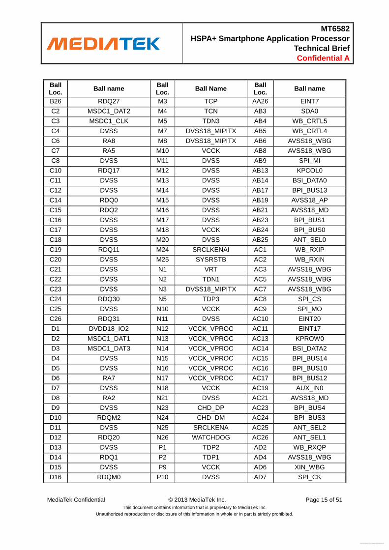
A7 RA4 J1 RDP2 V25 PCM_SYNC
A8 RA3 J2 RDN2 V26 PCM_RX
A10 RDQ19 J3 RDP1_A W1 DVDD18_IO3
A11 RDQ23 J5 DVSS18_MIPIIO W2 URXD0
A13 RDQ21 J7 DVSS18_MIPIIO W5 I2S_DATA_IN
A14 RDQ22 J21 DVSS W7 AVSS18_WBG
A16 RDQ4 J23 PWRAP_SPI0_CSN W20 AVSS18_MD
A17 RDQ6 J24 PWRAP_SPI0_MI W21 AVSS18_MD
A19 DVSS J25 AUD_DAT_MOSI W22 EINT0
A20 RDQ9 K1 RDP1 W25 EINT4
A22 RDQ12 K2 RDN1 Y2 UTXD0
A23 RDQ25 K3 RDN0 Y3 DSI_TE
A25 RDQ29 K5 RCN Y6 WB_CRTL0
A26 DVSS K6 RCP Y7 AVSS18_WBG
B1 CMPCLK K21 DVSS Y10 F2W_DATA
B2 CMMCLK K23 SIM1_SIO Y13 KPCOL2
B3 REXTDN K24 SIM2_SRST Y14 BSI_CLK
B4 DVSS K25 AUD_DAT_MISO Y15 BPI_BUS15
B5 RCKE K26 AUD_CLK_MOSI Y20 AVSS18_MD
B6 RCS1_B L2 DVDD18_MIPITX Y21 AVSS18_MD
B7 RCS0_B L3 RDP0 Y22 EINT10
B8 RA0 L4 DVSS18_MIPITX Y23 EINT9
B9 RA1 L10 DVSS Y25 EINT5
B10 DVSS L11 VCCK Y26 DVDD18_IO1
B11 RDQ16 L12 VCCK AA1 SCL2
B12 DVSS L13 VCCK AA2 SDA2
B13 RDQ18 L14 VCCK AA3 SCL0
B14 DVSS L15 VCCK AA4 WB_CRTL3
B15 RDQ3 L16 VCCK AA5 WB_CRTL2
B16 RDQ7 L17 VCCK AA6 WB_CRTL1
B17 DVSS L18 DVSS AA10 F2W_CLK
B18 RDQ5 L20 SIM2_SCLK AA13 KPROW2
B19 RDQ10 L21 SIM1_SCLK AA14 BSI_DATA1
B20 RDQ14 L23 SIM1_SRST AA17 BPI_BUS8
B21 RDQ8 L24 SIM2_SIO AA18 AVSS18_AP
B22 DVSS L25 RTC32K_CK AA21 AVSS18_MD
B23 RDQ26 L26 DVDD18_IO0 AA23 EINT6
B24 DVSS M1 TDP0 AA24 EINT2
B25 RDQ28 M2 TDN0 AA25 EINT8
Free Datasheet http://www.nDatasheet.com
[email protected],time=2013-08-10 09:29:21,ip=112.90.37.152,doctitle=MT6582WG_Technical_Brief_v1.1.docx,company=Hexing_WCX
MT6582
HSPA+ Smartphone Application Processor
Technical Brief
Confidential A
MediaTek Confidential © 2013 MediaTek Inc. Page 15 of 51
This document contains information that is proprietary to MediaTek Inc.
Unauthorized reproduction or disclosure of this information in whole or in part is strictly prohibited.
Ball Loc.
Ball name Ball Loc.
Ball Name Ball Loc.
Ball name
B26 RDQ27 M3 TCP AA26 EINT7
C2 MSDC1_DAT2 M4 TCN AB3 SDA0
C3 MSDC1_CLK M5 TDN3 AB4 WB_CRTL5
C4 DVSS M7 DVSS18_MIPITX AB5 WB_CRTL4
C6 RA8 M8 DVSS18_MIPITX AB6 AVSS18_WBG
C7 RA5 M10 VCCK AB8 AVSS18_WBG
C8 DVSS M11 DVSS AB9 SPI_MI
C10 RDQ17 M12 DVSS AB13 KPCOL0
C11 DVSS M13 DVSS AB14 BSI_DATA0
C12 DVSS M14 DVSS AB17 BPI_BUS13
C14 RDQ0 M15 DVSS AB19 AVSS18_AP
C15 RDQ2 M16 DVSS AB21 AVSS18_MD
C16 DVSS M17 DVSS AB23 BPI_BUS1
C17 DVSS M18 VCCK AB24 BPI_BUS0
C18 DVSS M20 DVSS AB25 ANT_SEL0
C19 RDQ11 M24 SRCLKENAI AC1 WB_RXIP
C20 DVSS M25 SYSRSTB AC2 WB_RXIN
C21 DVSS N1 VRT AC3 AVSS18_WBG
C22 DVSS N2 TDN1 AC5 AVSS18_WBG
C23 DVSS N3 DVSS18_MIPITX AC7 AVSS18_WBG
C24 RDQ30 N5 TDP3 AC8 SPI_CS
C25 DVSS N10 VCCK AC9 SPI_MO
C26 RDQ31 N11 DVSS AC10 EINT20
D1 DVDD18_IO2 N12 VCCK_VPROC AC11 EINT17
D2 MSDC1_DAT1 N13 VCCK_VPROC AC13 KPROW0
D3 MSDC1_DAT3 N14 VCCK_VPROC AC14 BSI_DATA2
D4 DVSS N15 VCCK_VPROC AC15 BPI_BUS14
D5 DVSS N16 VCCK_VPROC AC16 BPI_BUS10
D6 RA7 N17 VCCK_VPROC AC17 BPI_BUS12
D7 DVSS N18 VCCK AC19 AUX_IN0
D8 RA2 N21 DVSS AC21 AVSS18_MD
D9 DVSS N23 CHD_DP AC23 BPI_BUS4
D10 RDQM2 N24 CHD_DM AC24 BPI_BUS3
D11 DVSS N25 SRCLKENA AC25 ANT_SEL2
D12 RDQ20 N26 WATCHDOG AC26 ANT_SEL1
D13 DVSS P1 TDP2 AD2 WB_RXQP
D14 RDQ1 P2 TDP1 AD4 AVSS18_WBG
D15 DVSS P9 VCCK AD6 XIN_WBG
D16 RDQM0 P10 DVSS AD7 SPI_CK
Free Datasheet http://www.nDatasheet.com
[email protected],time=2013-08-10 09:29:21,ip=112.90.37.152,doctitle=MT6582WG_Technical_Brief_v1.1.docx,company=Hexing_WCX
MT6582
HSPA+ Smartphone Application Processor
Technical Brief
Confidential A
MediaTek Confidential © 2013 MediaTek Inc. Page 16 of 51
This document contains information that is proprietary to MediaTek Inc.
Unauthorized reproduction or disclosure of this information in whole or in part is strictly prohibited.
Ball Loc.
Ball name Ball Loc.
Ball Name Ball Loc.
Ball name
D17 DVSS P11 DVSS AD8 SCL1
D18 RDQM1 P12 DVSS AD9 DISP_PWM
D20 RDQ13 P13 DVSS AD10 EINT18
D21 DVSS P14 VCCK_VPROC AD13 KPCOL1
D22 RDQ15 P15 VCCK_VPROC AD14 BSI_EN
D23 RDQM3 P16 DVSS AD16 BPI_BUS9
D24 DVSS P17 DVSS AD19 AUX_IN1
D25 RDQ24 P18 VCCK AD22 AVSS18_MD
D26 MSDC0_CLK P21 DVSS AD24 BPI_BUS6
E1 DVDD28_MSDC1 P22 URXD2 AD25 BPI_BUS2
E2 CMDAT0 P23 UTXD2 AD26 DVDD28_BPI
E3 MSDC1_CMD P25 USB_VRT AE1 WB_TXIP
E4 MSDC1_DAT0 P26 AVDD18_USB AE2 WB_RXQN
E5 DVSS R1 TDN2 AE3 AVSS18_WBG
E7 DVDD12_EMI R2 DVSS AE4 AVDD18_WBG
E8 DVSS R4 DVDD18_EFUSE AE5 AVSS18_WBG
E9 RCLK0 R5 FSOURCE_P AE6 WB_SEN
E10 DVSS R7 MSDC2_CLK AE7 SDA1
E12 RDQS2_B R9 VCCK AE9 EINT19
E15 RDQS0_B R10 VCCK AE10 EINT16
E17 RDQS1_B R11 DVSS AE12 JTDO
E18 DVSS R12 VCCK_VPROC AE13 KPROW1
E20 RDQS3 R13 VCCK_VPROC AE14 TXBPI
E21 DVSS R14 VCCK_VPROC AE18 DVDD18_PLLGP
E23 MSDC0_DAT6 R15 VCCK_VPROC AE19 AVDD18_AP
E24 MSDC0_CMD R16 VCCK_VPROC AE21 AVDD18_MD
E25 MSDC0_DAT2 R17 VCCK_VPROC AE22 AVDD28_DAC
E26 MSDC0_DAT3 R18 VCCK AE24 APC
F2 CMDAT1 R23 URXD3 AE25 BPI_BUS5
F5 RCP_A T23 UTXD3 AF1 WB_TXIN
F6 DVSS R24 AVSS33_USB AF2 WB_TXQN
F7 DVDD12_EMI R25 USB_DM AF3 AVSS18_WBG
F8 DVDD12_EMI R26 USB_DP AF4 GPS_RXIP
F9 RCLK0_B T1 MSDC2_DAT2 AF5 GPS_RXQN
F12 RDQS2 T2 MSDC2_DAT3 AF6 WB_RSTB
F15 RDQS0 T3 MSDC2_CMD AF7 WB_SDATA
F16 VREF T5 MSDC2_DAT1 AF8 EINT14
F17 RDQS1 T6 MSDC2_DAT0 AF9 GPIO13
F18 DVSS T10 VCCK AF10 EINT11
Free Datasheet http://www.nDatasheet.com
[email protected],time=2013-08-10 09:29:21,ip=112.90.37.152,doctitle=MT6582WG_Technical_Brief_v1.1.docx,company=Hexing_WCX
MT6582
HSPA+ Smartphone Application Processor
Technical Brief
Confidential A
MediaTek Confidential © 2013 MediaTek Inc. Page 17 of 51
This document contains information that is proprietary to MediaTek Inc.
Unauthorized reproduction or disclosure of this information in whole or in part is strictly prohibited.
Ball Loc.
Ball name Ball Loc.
Ball Name Ball Loc.
Ball name
F20 RDQS3_B T11 DVSS AF11 TESTMODE
F22 MSDC0_DAT7 T12 DVSS AF12 JTCK
F24 MSDC0_DAT5 T13 DVSS AF13 JTMS
G1 DVDD18_MIPIIO T14 VCCK_VPROC AF14 VM1
G2 RDP3 T15 VCCK_VPROC AF15 BPI_BUS11
G3 RDN0_A T16 DVSS AF16 BPI_BUS7
G4 RDP0_A T17 DVSS AF17 AUX_YP
G5 RCN_A T18 DVSS AF18 AUX_XP
G6 DVSS T21 DVSS AF19 AVSS_REFN
G7 DVSS T24 AVDD33_USB AF20 UL_Q_N
G8 DVDD12_EMI U2 UTXD1 AF21 UL_I_N
G9 DVDD12_EMI U3 LCM_RST AF22 UL_I_P
G11 DVDD12_EMI U5 I2S_LRCK AF25 VBIAS
G13 DVDD12_EMI U7 AVSS18_WBG AF26 CLK26M
G14 DVSS U10 VCCK AG1 AVSS18_WBG
G15 DVDD12_EMI U11 DVSS AG2 WB_TXQP
G16 DVDD12_EMI U12 DVSS AG4 GPS_RXIN
G17 DVSS U15 VCCK_VPROC AG5 GPS_RXQP
G18 DVDD12_EMI U16 VCCK_VPROC AG7 WB_SCLK
G20 DVSS U17 AVSS18_AP AG8 EINT15
G22 MSDC0_DAT0 U18 AVSS18_AP AG10 GPIO12
G23 MSDC0_DAT1 U20 AVSS18_MD AG11 JTDI
G24 MSDC0_DAT4 U21 AVSS18_MD AG13 DVDD18_IO4
G25 MSDC0_RSTB U24 PCM_TX AG14 VM0
G26 DVDD18_MSDC0 U25 DVDD18_IO1 AG16 AUX_YM
H2 RDN3 V1 DVDD28_MSDC2 AG17 AUX_XM
H3 RDN1_A V2 URXD1 AG19 REFP
H4 DVSS18_MIPIIO V5 I2S_BCK AG20 UL_Q_P
H5 DVSS18_MIPIIO V7 AVSS18_WBG AG22 DL_Q_P
H8 DVDD12_EMI V10 VCCK AG23 DL_Q_N
H10 DVSS V11 DVSS AG24 DL_I_N
H11 DVDD12_EMI V12 DVSS AG25 DL_I_P
H12 DVSS V13 DVSS AG26 AVSS18_MD
H13 DVDD12_EMI V14 DVSS
H14 DVSS V15 VCCK_VPROC
H15 DVDD12_EMI V16 VCCK_VPROC
H16 DVDD12_EMI V17 AVSS18_AP
H17 DVSS V18 AVSS18_AP
Free Datasheet http://www.nDatasheet.com
[email protected],time=2013-08-10 09:29:21,ip=112.90.37.152,doctitle=MT6582WG_Technical_Brief_v1.1.docx,company=Hexing_WCX
MT6582
HSPA+ Smartphone Application Processor
Technical Brief
Confidential A
MediaTek Confidential © 2013 MediaTek Inc. Page 18 of 51
This document contains information that is proprietary to MediaTek Inc.
Unauthorized reproduction or disclosure of this information in whole or in part is strictly prohibited.
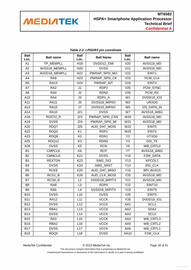
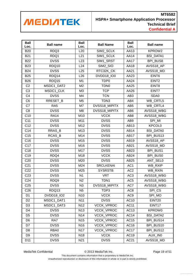
Table 2-2. LPDDR3 pin coordinate
Ball Loc.
Ball name Ball Loc.
Ball Name Ball Loc.
Ball name
A1 TP_MEMPLL H18 DVDD12_EMI V20 AVSS18_MD
A2 AVSS18_MEMPLL H20 DVSS V21 AVSS18_MD
A3 AVDD18_MEMPLL H22 PWRAP_SPI0_MO V22 EINT1
A4 RA9 H23 PWRAP_SPI0_CK V23 PCM_CLK
A5 RA13 H24 PWRAP_INT V24 EINT3
A7 RA2 J1 RDP2 V25 PCM_SYNC
A8 RA0 J2 RDN2 V26 PCM_RX
A10 RA4 J3 RDP1_A W1 DVDD18_IO3
A11 RA11 J5 DVSS18_MIPIIO W2 URXD0
A13 RA15 J7 DVSS18_MIPIIO W5 I2S_DATA_IN
A14 RA10 J21 DVSS W7 AVSS18_WBG
A16 RODT0_R J23 PWRAP_SPI0_CSN W20 AVSS18_MD
A19 DVSS J24 PWRAP_SPI0_MI W21 AVSS18_MD
A20 RDQ7 J25 AUD_DAT_MOSI W22 EINT0
A22 RDQ0 K1 RDP1 W25 EINT4
A23 RDQ8 K2 RDN1 Y2 UTXD0
A25 RDQ12 K3 RDN0 Y3 DSI_TE
A26 DVSS K5 RCN Y6 WB_CRTL0
B1 CMPCLK K6 RCP Y7 AVSS18_WBG
B2 CMMCLK K21 DVSS Y10 F2W_DATA
B3 REXTDN K23 SIM1_SIO Y13 KPCOL2
B4 DVSS K24 SIM2_SRST Y14 BSI_CLK
B5 RCKE K25 AUD_DAT_MISO Y15 BPI_BUS15
B6 RCS1_B K26 AUD_CLK_MOSI Y20 AVSS18_MD
B7 RCS0_B L2 DVDD18_MIPITX Y21 AVSS18_MD
B8 RA8 L3 RDP0 Y22 EINT10
B9 RA6 L4 DVSS18_MIPITX Y23 EINT9
B10 DVSS L10 DVSS Y25 EINT5
B11 RA12 L11 VCCK Y26 DVDD18_IO1
B12 DVSS L12 VCCK AA1 SCL2
B13 RBA1 L13 VCCK AA2 SDA2
B14 DVSS L14 VCCK AA3 SCL0
B15 RA3 L15 VCCK AA4 WB_CRTL3
B16 RBA2 L16 VCCK AA5 WB_CRTL2
B17 DVSS L17 VCCK AA6 WB_CRTL1
B19 RDQ5 L18 DVSS AA10 F2W_CLK
Free Datasheet http://www.nDatasheet.com
[email protected],time=2013-08-10 09:29:21,ip=112.90.37.152,doctitle=MT6582WG_Technical_Brief_v1.1.docx,company=Hexing_WCX
MT6582
HSPA+ Smartphone Application Processor
Technical Brief
Confidential A
MediaTek Confidential © 2013 MediaTek Inc. Page 19 of 51
This document contains information that is proprietary to MediaTek Inc.
Unauthorized reproduction or disclosure of this information in whole or in part is strictly prohibited.
Ball Loc.
Ball name Ball Loc.
Ball Name Ball Loc.
Ball name
B20 RDQ3 L20 SIM2_SCLK AA13 KPROW2
B21 RDQ1 L21 SIM1_SCLK AA14 BSI_DATA1
B22 DVSS L23 SIM1_SRST AA17 BPI_BUS8
B23 RDQ10 L24 SIM2_SIO AA18 AVSS18_AP
B24 DVSS L25 RTC32K_CK AA21 AVSS18_MD
B25 RDQ14 L26 DVDD18_IO0 AA23 EINT6
B26 RDQ15 M1 TDP0 AA24 EINT2
C2 MSDC1_DAT2 M2 TDN0 AA25 EINT8
C3 MSDC1_CLK M3 TCP AA26 EINT7
C4 DVSS M4 TCN AB3 SDA0
C6 RRESET_B M5 TDN3 AB4 WB_CRTL5
C7 RA5 M7 DVSS18_MIPITX AB5 WB_CRTL4
C8 DVSS M8 DVSS18_MIPITX AB6 AVSS18_WBG
C10 RA14 M10 VCCK AB8 AVSS18_WBG
C11 DVSS M11 DVSS AB9 SPI_MI
C12 DVSS M12 DVSS AB13 KPCOL0
C14 RRAS_B M13 DVSS AB14 BSI_DATA0
C15 RCAS_B M14 DVSS AB17 BPI_BUS13
C16 DVSS M15 DVSS AB19 AVSS18_AP
C17 DVSS M16 DVSS AB21 AVSS18_MD
C18 DVSS M17 DVSS AB23 BPI_BUS1
C19 RDQ4 M18 VCCK AB24 BPI_BUS0
C20 DVSS M20 DVSS AB25 ANT_SEL0
C21 DVSS M24 SRCLKENAI AC1 WB_RXIP
C22 DVSS M25 SYSRSTB AC2 WB_RXIN
C23 DVSS N1 VRT AC3 AVSS18_WBG
C24 RDQ9 N2 TDN1 AC5 AVSS18_WBG
C25 DVSS N3 DVSS18_MIPITX AC7 AVSS18_WBG
C26 RDQ13 N5 TDP3 AC8 SPI_CS
D1 DVDD18_IO2 N10 VCCK AC9 SPI_MO
D2 MSDC1_DAT1 N11 DVSS AC10 EINT20
D3 MSDC1_DAT3 N12 VCCK_VPROC AC11 EINT17
D4 DVSS N13 VCCK_VPROC AC13 KPROW0
D5 DVSS N14 VCCK_VPROC AC14 BSI_DATA2
D6 RA7 N15 VCCK_VPROC AC15 BPI_BUS14
D7 DVSS N16 VCCK_VPROC AC16 BPI_BUS10
D8 RBA0 N17 VCCK_VPROC AC17 BPI_BUS12
D9 DVSS N18 VCCK AC19 AUX_IN0
D11 DVSS N21 DVSS AC21 AVSS18_MD
Free Datasheet http://www.nDatasheet.com
[email protected],time=2013-08-10 09:29:21,ip=112.90.37.152,doctitle=MT6582WG_Technical_Brief_v1.1.docx,company=Hexing_WCX
MT6582
HSPA+ Smartphone Application Processor
Technical Brief
Confidential A
MediaTek Confidential © 2013 MediaTek Inc. Page 20 of 51
This document contains information that is proprietary to MediaTek Inc.
Unauthorized reproduction or disclosure of this information in whole or in part is strictly prohibited.
Ball Loc.
Ball name Ball Loc.
Ball Name Ball Loc.
Ball name
D12 RA1 N23 CHD_DP AC23 BPI_BUS4
D13 DVSS N24 CHD_DM AC24 BPI_BUS3
D14 RWR_B N25 SRCLKENA AC25 ANT_SEL2
D15 DVSS N26 WATCHDOG AC26 ANT_SEL1
D17 DVSS P1 TDP2 AD2 WB_RXQP
D18 RDQM0 P2 TDP1 AD4 AVSS18_WBG
D20 RDQ6 P9 VCCK AD6 XIN_WBG
D21 DVSS P10 DVSS AD7 SPI_CK
D22 RDQ2 P11 DVSS AD8 SCL1
D23 RDQM1 P12 DVSS AD9 DISP_PWM
D24 DVSS P13 DVSS AD10 EINT18
D25 RDQ11 P14 VCCK_VPROC AD13 KPCOL1
D26 MSDC0_CLK P15 VCCK_VPROC AD14 BSI_EN
E1 DVDD28_MSDC1 P16 DVSS AD16 BPI_BUS9
E2 CMDAT0 P17 DVSS AD19 AUX_IN1
E3 MSDC1_CMD P18 VCCK AD22 AVSS18_MD
E4 MSDC1_DAT0 P21 DVSS AD24 BPI_BUS6
E5 DVSS P22 URXD2 AD25 BPI_BUS2
E7 DVDD12_EMI P23 UTXD2 AD26 DVDD28_BPI
E8 DVSS P25 USB_VRT AE1 WB_TXIP
E9 RCLK0 P26 AVDD18_USB AE2 WB_RXQN
E10 DVSS R1 TDN2 AE3 AVSS18_WBG
E17 RDQS0_B R2 DVSS AE4 AVDD18_WBG
E18 DVSS R4 DVDD18_EFUSE AE5 AVSS18_WBG
E20 RDQS1 R5 FSOURCE_P AE6 WB_SEN
E21 DVSS R7 MSDC2_CLK AE7 SDA1
E23 MSDC0_DAT6 R9 VCCK AE9 EINT19
E24 MSDC0_CMD R10 VCCK AE10 EINT16
E25 MSDC0_DAT2 R11 DVSS AE12 JTDO
E26 MSDC0_DAT3 R12 VCCK_VPROC AE13 KPROW1
F2 CMDAT1 R13 VCCK_VPROC AE14 TXBPI
F5 RCP_A R14 VCCK_VPROC AE18 DVDD18_PLLGP
F6 DVSS R15 VCCK_VPROC AE19 AVDD18_AP
F7 DVDD12_EMI R16 VCCK_VPROC AE21 AVDD18_MD
F8 DVDD12_EMI R17 VCCK_VPROC AE22 AVDD28_DAC
F9 RCLK0_B R18 VCCK AE24 APC
F16 VREF R23 URXD3 AE25 BPI_BUS5
F17 RDQS0 R24 AVSS33_USB AF1 WB_TXIN
F18 DVSS R25 USB_DM AF2 WB_TXQN
Free Datasheet http://www.nDatasheet.com
[email protected],time=2013-08-10 09:29:21,ip=112.90.37.152,doctitle=MT6582WG_Technical_Brief_v1.1.docx,company=Hexing_WCX
MT6582
HSPA+ Smartphone Application Processor
Technical Brief
Confidential A
MediaTek Confidential © 2013 MediaTek Inc. Page 21 of 51
This document contains information that is proprietary to MediaTek Inc.
Unauthorized reproduction or disclosure of this information in whole or in part is strictly prohibited.
Ball Loc.
Ball name Ball Loc.
Ball Name Ball Loc.
Ball name
F20 RDQS1_B R26 USB_DP AF3 AVSS18_WBG
F22 MSDC0_DAT7 T1 MSDC2_DAT2 AF4 GPS_RXIP
F24 MSDC0_DAT5 T2 MSDC2_DAT3 AF5 GPS_RXQN
G1 DVDD18_MIPIIO T3 MSDC2_CMD AF6 WB_RSTB
G2 RDP3 T5 MSDC2_DAT1 AF7 WB_SDATA
G3 RDN0_A T6 MSDC2_DAT0 AF8 EINT14
G4 RDP0_A T10 VCCK AF9 GPIO13
G5 RCN_A T11 DVSS AF10 EINT11
G6 DVSS T12 DVSS AF11 TESTMODE
G7 DVSS T13 DVSS AF12 JTCK
G8 DVDD12_EMI T14 VCCK_VPROC AF13 JTMS
G9 DVDD12_EMI T15 VCCK_VPROC AF14 VM1
G11 DVDD12_EMI T16 DVSS AF15 BPI_BUS11
G13 DVDD12_EMI T17 DVSS AF16 BPI_BUS7
G14 DVSS T18 DVSS AF17 AUX_YP
G15 DVDD12_EMI T21 DVSS AF18 AUX_XP
G16 DVDD12_EMI T23 UTXD3 AF19 AVSS_REFN
G17 DVSS T24 AVDD33_USB AF20 UL_Q_N
G18 DVDD12_EMI U2 UTXD1 AF21 UL_I_N
G20 DVSS U3 LCM_RST AF22 UL_I_P
G22 MSDC0_DAT0 U5 I2S_LRCK AF25 VBIAS
G23 MSDC0_DAT1 U7 AVSS18_WBG AF26 CLK26M
G24 MSDC0_DAT4 U10 VCCK AG1 AVSS18_WBG
G25 MSDC0_RSTB U11 DVSS AG2 WB_TXQP
G26 DVDD18_MSDC0 U12 DVSS AG4 GPS_RXIN
H2 RDN3 U15 VCCK_VPROC AG5 GPS_RXQP
H3 RDN1_A U16 VCCK_VPROC AG7 WB_SCLK
H4 DVSS18_MIPIIO U17 AVSS18_AP AG8 EINT15
H5 DVSS18_MIPIIO U18 AVSS18_AP AG10 GPIO12
H8 DVDD12_EMI U20 AVSS18_MD AG11 JTDI
H10 DVSS U21 AVSS18_MD AG13 DVDD18_IO4
H11 DVDD12_EMI U24 PCM_TX AG14 VM0
H12 DVSS U25 DVDD18_IO1 AG16 AUX_YM
H13 DVDD12_EMI V1 DVDD28_MSDC2 AG17 AUX_XM
H14 DVSS V2 URXD1 AG19 REFP
H15 DVDD12_EMI V5 I2S_BCK AG20 UL_Q_P
H16 DVDD12_EMI V7 AVSS18_WBG AG22 DL_Q_P
H17 DVSS V10 VCCK AG23 DL_Q_N
A1 TP_MEMPLL V11 DVSS AG24 DL_I_N
Free Datasheet http://www.nDatasheet.com
[email protected],time=2013-08-10 09:29:21,ip=112.90.37.152,doctitle=MT6582WG_Technical_Brief_v1.1.docx,company=Hexing_WCX
MT6582
HSPA+ Smartphone Application Processor
Technical Brief
Confidential A
MediaTek Confidential © 2013 MediaTek Inc. Page 22 of 51
This document contains information that is proprietary to MediaTek Inc.
Unauthorized reproduction or disclosure of this information in whole or in part is strictly prohibited.
Ball Loc.
Ball name Ball Loc.
Ball Name Ball Loc.
Ball name
A2 AVSS18_MEMPLL V12 DVSS AG25 DL_I_P
A3 AVDD18_MEMPLL V13 DVSS AG26 AVSS18_MD
A4 RA9 V14 DVSS
A5 RA13 V15 VCCK_VPROC
A7 RA2 V16 VCCK_VPROC
A8 RA0 V17 AVSS18_AP
A10 RA4 V18 AVSS18_AP
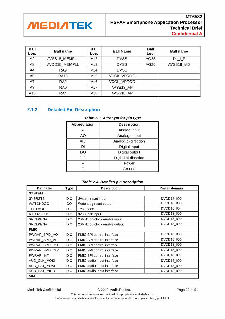
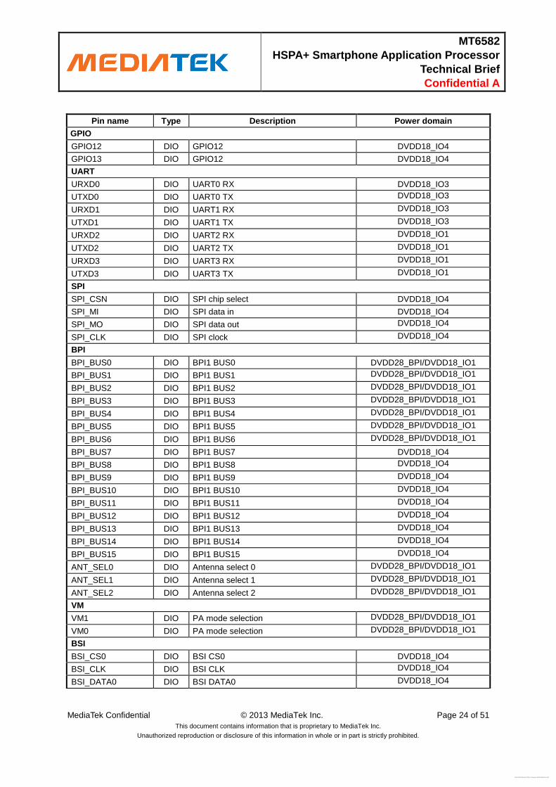
2.1.2 Detailed Pin Description
Table 2-3. Acronym for pin type
Abbreviation Description
AI Analog input
AO Analog output
AIO Analog bi-direction
DI Digital input
DO Digital output
DIO Digital bi-direction
P Power
G Ground
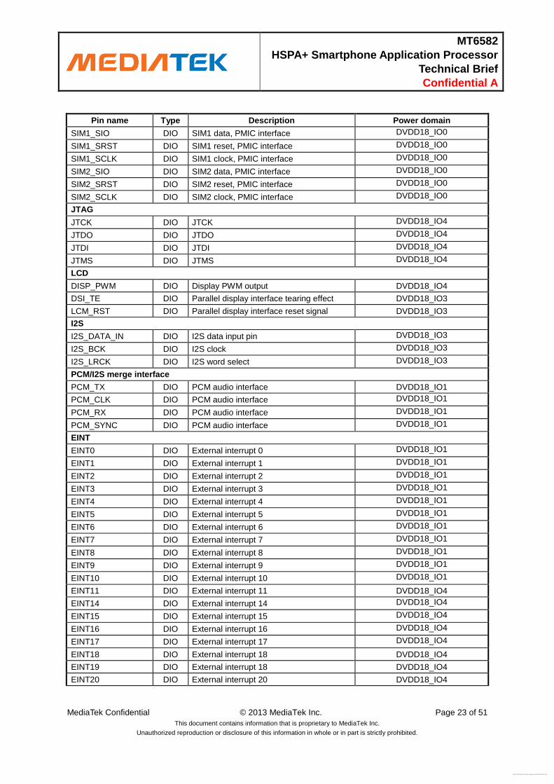
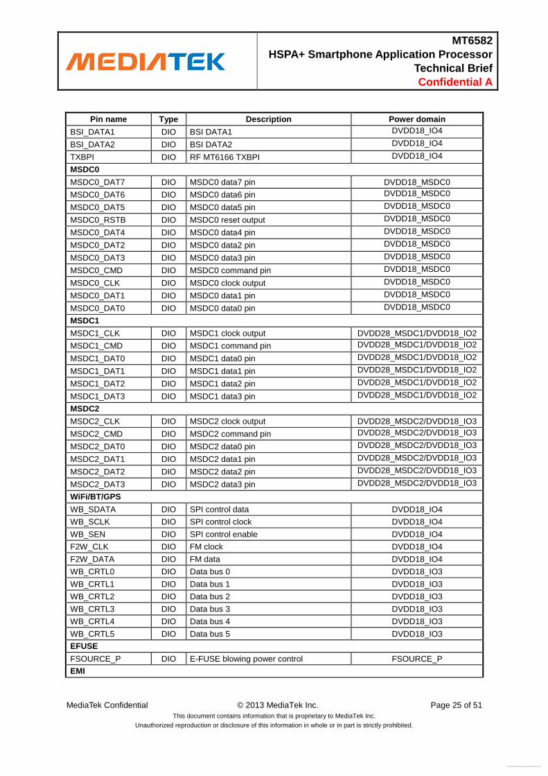
Table 2-4. Detailed pin description
Pin name Type Description Power domain
SYSTEM
SYSRSTB DIO System reset input DVDD18_IO0
WATCHDOG DO Watchdog reset output DVDD18_IO0
TESTMODE DIO Test mode DVDD18_IO4
RTC32K_CK DIO 32K clock input DVDD18_IO0
SRCLKENAI DIO 26MHz co-clock enable input DVDD18_IO0
SRCLKENA DIO 26MHz co-clock enable output DVDD18_IO0
PMIC
PWRAP_SPI0_MO DIO PMIC SPI control interface DVDD18_IO0
PWRAP_SPI0_MI DIO PMIC SPI control interface DVDD18_IO0
PWRAP_SPI0_CSN DIO PMIC SPI control interface DVDD18_IO0
PWRAP_SPI0_CLK DIO PMIC SPI control interface DVDD18_IO0
PWRAP_INT DIO PMIC SPI control interface DVDD18_IO0
AUD_CLK_MOSI DIO PMIC audio input interface DVDD18_IO0
AUD_DAT_MOSI DIO PMIC audio input interface DVDD18_IO0
AUD_DAT_MISO DIO PMIC audio input interface DVDD18_IO0
SIM
Free Datasheet http://www.nDatasheet.com
[email protected],time=2013-08-10 09:29:21,ip=112.90.37.152,doctitle=MT6582WG_Technical_Brief_v1.1.docx,company=Hexing_WCX
MT6582
HSPA+ Smartphone Application Processor
Technical Brief
Confidential A
MediaTek Confidential © 2013 MediaTek Inc. Page 23 of 51
This document contains information that is proprietary to MediaTek Inc.
Unauthorized reproduction or disclosure of this information in whole or in part is strictly prohibited.
Pin name Type Description Power domain
SIM1_SIO DIO SIM1 data, PMIC interface DVDD18_IO0
SIM1_SRST DIO SIM1 reset, PMIC interface DVDD18_IO0
SIM1_SCLK DIO SIM1 clock, PMIC interface DVDD18_IO0
SIM2_SIO DIO SIM2 data, PMIC interface DVDD18_IO0
SIM2_SRST DIO SIM2 reset, PMIC interface DVDD18_IO0
SIM2_SCLK DIO SIM2 clock, PMIC interface DVDD18_IO0
JTAG
JTCK DIO JTCK DVDD18_IO4
JTDO DIO JTDO DVDD18_IO4
JTDI DIO JTDI DVDD18_IO4
JTMS DIO JTMS DVDD18_IO4
LCD
DISP_PWM DIO Display PWM output DVDD18_IO4
DSI_TE DIO Parallel display interface tearing effect DVDD18_IO3
LCM_RST DIO Parallel display interface reset signal DVDD18_IO3
I2S
I2S_DATA_IN DIO I2S data input pin DVDD18_IO3
I2S_BCK DIO I2S clock DVDD18_IO3
I2S_LRCK DIO I2S word select DVDD18_IO3
PCM/I2S merge interface
PCM_TX DIO PCM audio interface DVDD18_IO1
PCM_CLK DIO PCM audio interface DVDD18_IO1
PCM_RX DIO PCM audio interface DVDD18_IO1
PCM_SYNC DIO PCM audio interface DVDD18_IO1
EINT
EINT0 DIO External interrupt 0 DVDD18_IO1
EINT1 DIO External interrupt 1 DVDD18_IO1
EINT2 DIO External interrupt 2 DVDD18_IO1
EINT3 DIO External interrupt 3 DVDD18_IO1
EINT4 DIO External interrupt 4 DVDD18_IO1
EINT5 DIO External interrupt 5 DVDD18_IO1
EINT6 DIO External interrupt 6 DVDD18_IO1
EINT7 DIO External interrupt 7 DVDD18_IO1
EINT8 DIO External interrupt 8 DVDD18_IO1
EINT9 DIO External interrupt 9 DVDD18_IO1
EINT10 DIO External interrupt 10 DVDD18_IO1
EINT11 DIO External interrupt 11 DVDD18_IO4
EINT14 DIO External interrupt 14 DVDD18_IO4
EINT15 DIO External interrupt 15 DVDD18_IO4
EINT16 DIO External interrupt 16 DVDD18_IO4
EINT17 DIO External interrupt 17 DVDD18_IO4
EINT18 DIO External interrupt 18 DVDD18_IO4
EINT19 DIO External interrupt 18 DVDD18_IO4
EINT20 DIO External interrupt 20 DVDD18_IO4
Free Datasheet http://www.nDatasheet.com
[email protected],time=2013-08-10 09:29:21,ip=112.90.37.152,doctitle=MT6582WG_Technical_Brief_v1.1.docx,company=Hexing_WCX
MT6582
HSPA+ Smartphone Application Processor
Technical Brief
Confidential A
MediaTek Confidential © 2013 MediaTek Inc. Page 24 of 51
This document contains information that is proprietary to MediaTek Inc.
Unauthorized reproduction or disclosure of this information in whole or in part is strictly prohibited.
Pin name Type Description Power domain
GPIO
GPIO12 DIO GPIO12 DVDD18_IO4
GPIO13 DIO GPIO12 DVDD18_IO4
UART
URXD0 DIO UART0 RX DVDD18_IO3
UTXD0 DIO UART0 TX DVDD18_IO3
URXD1 DIO UART1 RX DVDD18_IO3
UTXD1 DIO UART1 TX DVDD18_IO3
URXD2 DIO UART2 RX DVDD18_IO1
UTXD2 DIO UART2 TX DVDD18_IO1
URXD3 DIO UART3 RX DVDD18_IO1
UTXD3 DIO UART3 TX DVDD18_IO1
SPI
SPI_CSN DIO SPI chip select DVDD18_IO4
SPI_MI DIO SPI data in DVDD18_IO4
SPI_MO DIO SPI data out DVDD18_IO4
SPI_CLK DIO SPI clock DVDD18_IO4
BPI
BPI_BUS0 DIO BPI1 BUS0 DVDD28_BPI/DVDD18_IO1
BPI_BUS1 DIO BPI1 BUS1 DVDD28_BPI/DVDD18_IO1
BPI_BUS2 DIO BPI1 BUS2 DVDD28_BPI/DVDD18_IO1
BPI_BUS3 DIO BPI1 BUS3 DVDD28_BPI/DVDD18_IO1
BPI_BUS4 DIO BPI1 BUS4 DVDD28_BPI/DVDD18_IO1
BPI_BUS5 DIO BPI1 BUS5 DVDD28_BPI/DVDD18_IO1
BPI_BUS6 DIO BPI1 BUS6 DVDD28_BPI/DVDD18_IO1
BPI_BUS7 DIO BPI1 BUS7 DVDD18_IO4
BPI_BUS8 DIO BPI1 BUS8 DVDD18_IO4
BPI_BUS9 DIO BPI1 BUS9 DVDD18_IO4
BPI_BUS10 DIO BPI1 BUS10 DVDD18_IO4
BPI_BUS11 DIO BPI1 BUS11 DVDD18_IO4
BPI_BUS12 DIO BPI1 BUS12 DVDD18_IO4
BPI_BUS13 DIO BPI1 BUS13 DVDD18_IO4
BPI_BUS14 DIO BPI1 BUS14 DVDD18_IO4
BPI_BUS15 DIO BPI1 BUS15 DVDD18_IO4
ANT_SEL0 DIO Antenna select 0 DVDD28_BPI/DVDD18_IO1
ANT_SEL1 DIO Antenna select 1 DVDD28_BPI/DVDD18_IO1
ANT_SEL2 DIO Antenna select 2 DVDD28_BPI/DVDD18_IO1
VM
VM1 DIO PA mode selection DVDD28_BPI/DVDD18_IO1
VM0 DIO PA mode selection DVDD28_BPI/DVDD18_IO1
BSI
BSI_CS0 DIO BSI CS0 DVDD18_IO4
BSI_CLK DIO BSI CLK DVDD18_IO4
BSI_DATA0 DIO BSI DATA0 DVDD18_IO4
Free Datasheet http://www.nDatasheet.com
[email protected],time=2013-08-10 09:29:21,ip=112.90.37.152,doctitle=MT6582WG_Technical_Brief_v1.1.docx,company=Hexing_WCX
MT6582
HSPA+ Smartphone Application Processor
Technical Brief
Confidential A
MediaTek Confidential © 2013 MediaTek Inc. Page 25 of 51
This document contains information that is proprietary to MediaTek Inc.
Unauthorized reproduction or disclosure of this information in whole or in part is strictly prohibited.
Pin name Type Description Power domain
BSI_DATA1 DIO BSI DATA1 DVDD18_IO4
BSI_DATA2 DIO BSI DATA2 DVDD18_IO4
TXBPI DIO RF MT6166 TXBPI DVDD18_IO4
MSDC0
MSDC0_DAT7 DIO MSDC0 data7 pin DVDD18_MSDC0
MSDC0_DAT6 DIO MSDC0 data6 pin DVDD18_MSDC0
MSDC0_DAT5 DIO MSDC0 data5 pin DVDD18_MSDC0
MSDC0_RSTB DIO MSDC0 reset output DVDD18_MSDC0
MSDC0_DAT4 DIO MSDC0 data4 pin DVDD18_MSDC0
MSDC0_DAT2 DIO MSDC0 data2 pin DVDD18_MSDC0
MSDC0_DAT3 DIO MSDC0 data3 pin DVDD18_MSDC0
MSDC0_CMD DIO MSDC0 command pin DVDD18_MSDC0
MSDC0_CLK DIO MSDC0 clock output DVDD18_MSDC0
MSDC0_DAT1 DIO MSDC0 data1 pin DVDD18_MSDC0
MSDC0_DAT0 DIO MSDC0 data0 pin DVDD18_MSDC0
MSDC1
MSDC1_CLK DIO MSDC1 clock output DVDD28_MSDC1/DVDD18_IO2
MSDC1_CMD DIO MSDC1 command pin DVDD28_MSDC1/DVDD18_IO2
MSDC1_DAT0 DIO MSDC1 data0 pin DVDD28_MSDC1/DVDD18_IO2
MSDC1_DAT1 DIO MSDC1 data1 pin DVDD28_MSDC1/DVDD18_IO2
MSDC1_DAT2 DIO MSDC1 data2 pin DVDD28_MSDC1/DVDD18_IO2
MSDC1_DAT3 DIO MSDC1 data3 pin DVDD28_MSDC1/DVDD18_IO2
MSDC2
MSDC2_CLK DIO MSDC2 clock output DVDD28_MSDC2/DVDD18_IO3
MSDC2_CMD DIO MSDC2 command pin DVDD28_MSDC2/DVDD18_IO3
MSDC2_DAT0 DIO MSDC2 data0 pin DVDD28_MSDC2/DVDD18_IO3
MSDC2_DAT1 DIO MSDC2 data1 pin DVDD28_MSDC2/DVDD18_IO3
MSDC2_DAT2 DIO MSDC2 data2 pin DVDD28_MSDC2/DVDD18_IO3
MSDC2_DAT3 DIO MSDC2 data3 pin DVDD28_MSDC2/DVDD18_IO3
WiFi/BT/GPS
WB_SDATA DIO SPI control data DVDD18_IO4
WB_SCLK DIO SPI control clock DVDD18_IO4
WB_SEN DIO SPI control enable DVDD18_IO4
F2W_CLK DIO FM clock DVDD18_IO4
F2W_DATA DIO FM data DVDD18_IO4
WB_CRTL0 DIO Data bus 0 DVDD18_IO3
WB_CRTL1 DIO Data bus 1 DVDD18_IO3
WB_CRTL2 DIO Data bus 2 DVDD18_IO3
WB_CRTL3 DIO Data bus 3 DVDD18_IO3
WB_CRTL4 DIO Data bus 4 DVDD18_IO3
WB_CRTL5 DIO Data bus 5 DVDD18_IO3
EFUSE
FSOURCE_P DIO E-FUSE blowing power control FSOURCE_P
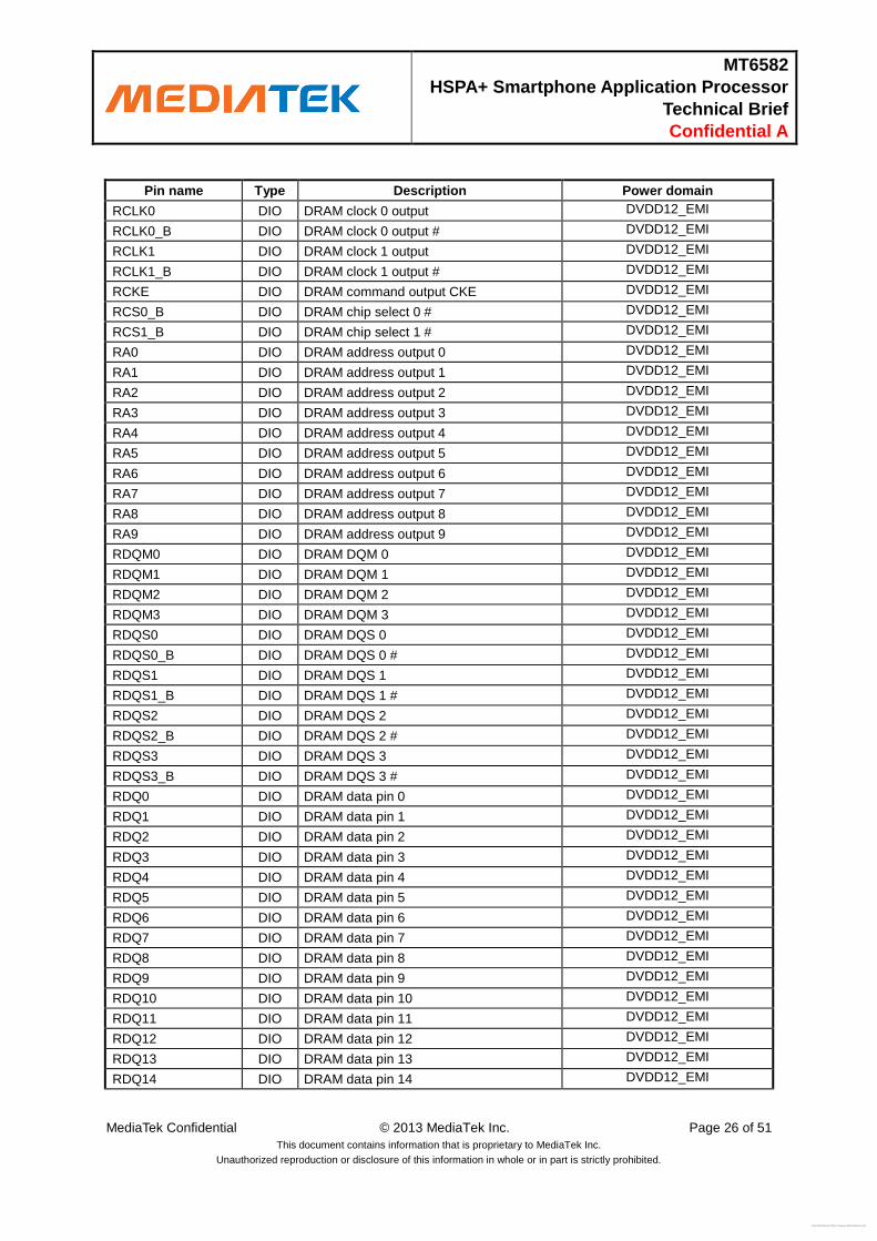
EMI
Free Datasheet http://www.nDatasheet.com
[email protected],time=2013-08-10 09:29:21,ip=112.90.37.152,doctitle=MT6582WG_Technical_Brief_v1.1.docx,company=Hexing_WCX
MT6582
HSPA+ Smartphone Application Processor
Technical Brief
Confidential A
MediaTek Confidential © 2013 MediaTek Inc. Page 26 of 51
This document contains information that is proprietary to MediaTek Inc.
Unauthorized reproduction or disclosure of this information in whole or in part is strictly prohibited.
Pin name Type Description Power domain
RCLK0 DIO DRAM clock 0 output DVDD12_EMI
RCLK0_B DIO DRAM clock 0 output # DVDD12_EMI
RCLK1 DIO DRAM clock 1 output DVDD12_EMI
RCLK1_B DIO DRAM clock 1 output # DVDD12_EMI
RCKE DIO DRAM command output CKE DVDD12_EMI
RCS0_B DIO DRAM chip select 0 # DVDD12_EMI
RCS1_B DIO DRAM chip select 1 # DVDD12_EMI
RA0 DIO DRAM address output 0 DVDD12_EMI
RA1 DIO DRAM address output 1 DVDD12_EMI
RA2 DIO DRAM address output 2 DVDD12_EMI
RA3 DIO DRAM address output 3 DVDD12_EMI
RA4 DIO DRAM address output 4 DVDD12_EMI
RA5 DIO DRAM address output 5 DVDD12_EMI
RA6 DIO DRAM address output 6 DVDD12_EMI
RA7 DIO DRAM address output 7 DVDD12_EMI
RA8 DIO DRAM address output 8 DVDD12_EMI
RA9 DIO DRAM address output 9 DVDD12_EMI
RDQM0 DIO DRAM DQM 0 DVDD12_EMI
RDQM1 DIO DRAM DQM 1 DVDD12_EMI
RDQM2 DIO DRAM DQM 2 DVDD12_EMI
RDQM3 DIO DRAM DQM 3 DVDD12_EMI
RDQS0 DIO DRAM DQS 0 DVDD12_EMI
RDQS0_B DIO DRAM DQS 0 # DVDD12_EMI
RDQS1 DIO DRAM DQS 1 DVDD12_EMI
RDQS1_B DIO DRAM DQS 1 # DVDD12_EMI
RDQS2 DIO DRAM DQS 2 DVDD12_EMI
RDQS2_B DIO DRAM DQS 2 # DVDD12_EMI
RDQS3 DIO DRAM DQS 3 DVDD12_EMI
RDQS3_B DIO DRAM DQS 3 # DVDD12_EMI
RDQ0 DIO DRAM data pin 0 DVDD12_EMI
RDQ1 DIO DRAM data pin 1 DVDD12_EMI
RDQ2 DIO DRAM data pin 2 DVDD12_EMI
RDQ3 DIO DRAM data pin 3 DVDD12_EMI
RDQ4 DIO DRAM data pin 4 DVDD12_EMI
RDQ5 DIO DRAM data pin 5 DVDD12_EMI
RDQ6 DIO DRAM data pin 6 DVDD12_EMI
RDQ7 DIO DRAM data pin 7 DVDD12_EMI
RDQ8 DIO DRAM data pin 8 DVDD12_EMI
RDQ9 DIO DRAM data pin 9 DVDD12_EMI
RDQ10 DIO DRAM data pin 10 DVDD12_EMI
RDQ11 DIO DRAM data pin 11 DVDD12_EMI
RDQ12 DIO DRAM data pin 12 DVDD12_EMI
RDQ13 DIO DRAM data pin 13 DVDD12_EMI
RDQ14 DIO DRAM data pin 14 DVDD12_EMI
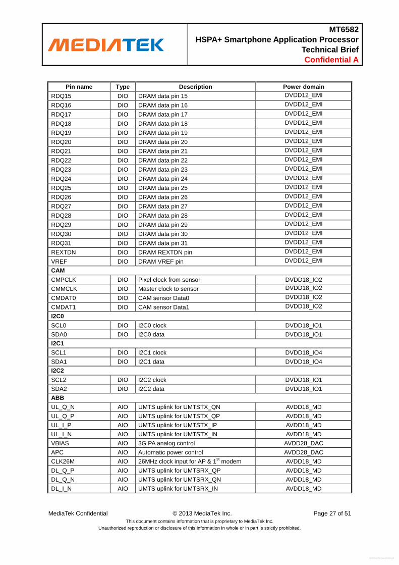
Free Datasheet http://www.nDatasheet.com
[email protected],time=2013-08-10 09:29:21,ip=112.90.37.152,doctitle=MT6582WG_Technical_Brief_v1.1.docx,company=Hexing_WCX
MT6582
HSPA+ Smartphone Application Processor
Technical Brief
Confidential A
MediaTek Confidential © 2013 MediaTek Inc. Page 27 of 51
This document contains information that is proprietary to MediaTek Inc.
Unauthorized reproduction or disclosure of this information in whole or in part is strictly prohibited.
Pin name Type Description Power domain
RDQ15 DIO DRAM data pin 15 DVDD12_EMI
RDQ16 DIO DRAM data pin 16 DVDD12_EMI
RDQ17 DIO DRAM data pin 17 DVDD12_EMI
RDQ18 DIO DRAM data pin 18 DVDD12_EMI
RDQ19 DIO DRAM data pin 19 DVDD12_EMI
RDQ20 DIO DRAM data pin 20 DVDD12_EMI
RDQ21 DIO DRAM data pin 21 DVDD12_EMI
RDQ22 DIO DRAM data pin 22 DVDD12_EMI
RDQ23 DIO DRAM data pin 23 DVDD12_EMI
RDQ24 DIO DRAM data pin 24 DVDD12_EMI
RDQ25 DIO DRAM data pin 25 DVDD12_EMI
RDQ26 DIO DRAM data pin 26 DVDD12_EMI
RDQ27 DIO DRAM data pin 27 DVDD12_EMI
RDQ28 DIO DRAM data pin 28 DVDD12_EMI
RDQ29 DIO DRAM data pin 29 DVDD12_EMI
RDQ30 DIO DRAM data pin 30 DVDD12_EMI
RDQ31 DIO DRAM data pin 31 DVDD12_EMI
REXTDN DIO DRAM REXTDN pin DVDD12_EMI
VREF DIO DRAM VREF pin DVDD12_EMI
CAM
CMPCLK DIO Pixel clock from sensor DVDD18_IO2
CMMCLK DIO Master clock to sensor DVDD18_IO2
CMDAT0 DIO CAM sensor Data0 DVDD18_IO2
CMDAT1 DIO CAM sensor Data1 DVDD18_IO2
I2C0
SCL0 DIO I2C0 clock DVDD18_IO1
SDA0 DIO I2C0 data DVDD18_IO1
I2C1
SCL1 DIO I2C1 clock DVDD18_IO4
SDA1 DIO I2C1 data DVDD18_IO4
I2C2
SCL2 DIO I2C2 clock DVDD18_IO1
SDA2 DIO I2C2 data DVDD18_IO1
ABB
UL_Q_N AIO UMTS uplink for UMTSTX_QN AVDD18_MD
UL_Q_P AIO UMTS uplink for UMTSTX_QP AVDD18_MD
UL_I_P AIO UMTS uplink for UMTSTX_IP AVDD18_MD
UL_I_N AIO UMTS uplink for UMTSTX_IN AVDD18_MD
VBIAS AIO 3G PA analog control AVDD28_DAC
APC AIO Automatic power control AVDD28_DAC
CLK26M AIO 26MHz clock input for AP & 1st modem AVDD18_MD
DL_Q_P AIO UMTS uplink for UMTSRX_QP AVDD18_MD
DL_Q_N AIO UMTS uplink for UMTSRX_QN AVDD18_MD
DL_I_N AIO UMTS uplink for UMTSRX_IN AVDD18_MD
Free Datasheet http://www.nDatasheet.com
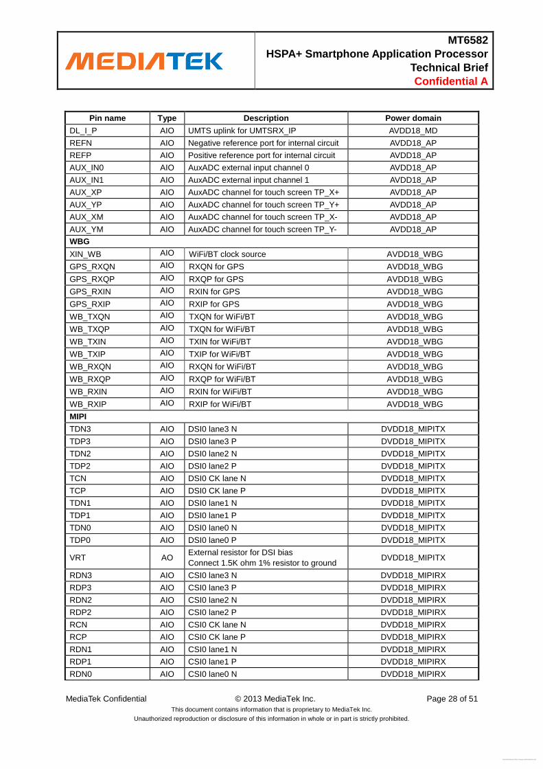
[email protected],time=2013-08-10 09:29:21,ip=112.90.37.152,doctitle=MT6582WG_Technical_Brief_v1.1.docx,company=Hexing_WCX
MT6582
HSPA+ Smartphone Application Processor
Technical Brief
Confidential A
MediaTek Confidential © 2013 MediaTek Inc. Page 28 of 51
This document contains information that is proprietary to MediaTek Inc.
Unauthorized reproduction or disclosure of this information in whole or in part is strictly prohibited.
Pin name Type Description Power domain
DL_I_P AIO UMTS uplink for UMTSRX_IP AVDD18_MD
REFN AIO Negative reference port for internal circuit AVDD18_AP
REFP AIO Positive reference port for internal circuit AVDD18_AP
AUX_IN0 AIO AuxADC external input channel 0 AVDD18_AP
AUX_IN1 AIO AuxADC external input channel 1 AVDD18_AP
AUX_XP AIO AuxADC channel for touch screen TP_X+ AVDD18_AP
AUX_YP AIO AuxADC channel for touch screen TP_Y+ AVDD18_AP
AUX_XM AIO AuxADC channel for touch screen TP_X- AVDD18_AP
AUX_YM AIO AuxADC channel for touch screen TP_Y- AVDD18_AP
WBG
XIN_WB AIO WiFi/BT clock source AVDD18_WBG
GPS_RXQN AIO RXQN for GPS AVDD18_WBG
GPS_RXQP AIO RXQP for GPS AVDD18_WBG
GPS_RXIN AIO RXIN for GPS AVDD18_WBG
GPS_RXIP AIO RXIP for GPS AVDD18_WBG
WB_TXQN AIO TXQN for WiFi/BT AVDD18_WBG
WB_TXQP AIO TXQN for WiFi/BT AVDD18_WBG
WB_TXIN AIO TXIN for WiFi/BT AVDD18_WBG
WB_TXIP AIO TXIP for WiFi/BT AVDD18_WBG
WB_RXQN AIO RXQN for WiFi/BT AVDD18_WBG
WB_RXQP AIO RXQP for WiFi/BT AVDD18_WBG
WB_RXIN AIO RXIN for WiFi/BT AVDD18_WBG
WB_RXIP AIO RXIP for WiFi/BT AVDD18_WBG
MIPI
TDN3 AIO DSI0 lane3 N DVDD18_MIPITX
TDP3 AIO DSI0 lane3 P DVDD18_MIPITX
TDN2 AIO DSI0 lane2 N DVDD18_MIPITX
TDP2 AIO DSI0 lane2 P DVDD18_MIPITX
TCN AIO DSI0 CK lane N DVDD18_MIPITX
TCP AIO DSI0 CK lane P DVDD18_MIPITX
TDN1 AIO DSI0 lane1 N DVDD18_MIPITX
TDP1 AIO DSI0 lane1 P DVDD18_MIPITX
TDN0 AIO DSI0 lane0 N DVDD18_MIPITX
TDP0 AIO DSI0 lane0 P DVDD18_MIPITX
VRT AO External resistor for DSI bias
Connect 1.5K ohm 1% resistor to ground DVDD18_MIPITX
RDN3 AIO CSI0 lane3 N DVDD18_MIPIRX
RDP3 AIO CSI0 lane3 P DVDD18_MIPIRX
RDN2 AIO CSI0 lane2 N DVDD18_MIPIRX
RDP2 AIO CSI0 lane2 P DVDD18_MIPIRX
RCN AIO CSI0 CK lane N DVDD18_MIPIRX
RCP AIO CSI0 CK lane P DVDD18_MIPIRX
RDN1 AIO CSI0 lane1 N DVDD18_MIPIRX
RDP1 AIO CSI0 lane1 P DVDD18_MIPIRX
RDN0 AIO CSI0 lane0 N DVDD18_MIPIRX
Free Datasheet http://www.nDatasheet.com
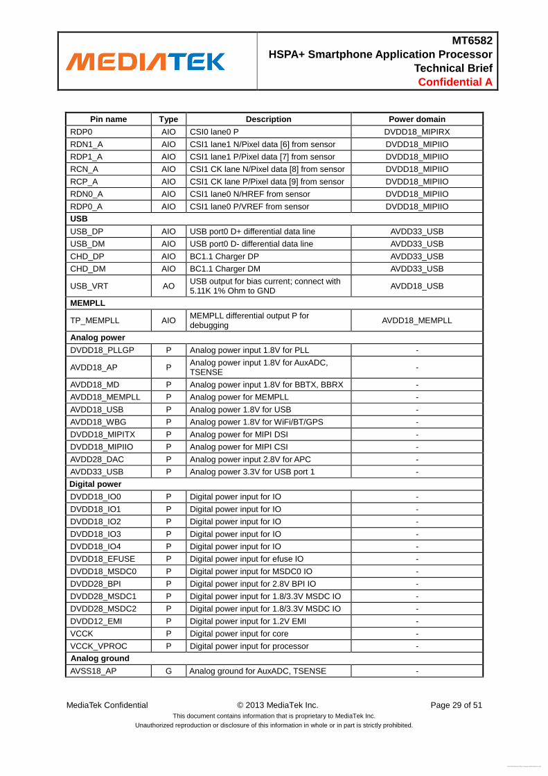
[email protected],time=2013-08-10 09:29:21,ip=112.90.37.152,doctitle=MT6582WG_Technical_Brief_v1.1.docx,company=Hexing_WCX
MT6582
HSPA+ Smartphone Application Processor
Technical Brief
Confidential A
MediaTek Confidential © 2013 MediaTek Inc. Page 29 of 51
This document contains information that is proprietary to MediaTek Inc.
Unauthorized reproduction or disclosure of this information in whole or in part is strictly prohibited.
Pin name Type Description Power domain
RDP0 AIO CSI0 lane0 P DVDD18_MIPIRX
RDN1_A AIO CSI1 lane1 N/Pixel data [6] from sensor DVDD18_MIPIIO
RDP1_A AIO CSI1 lane1 P/Pixel data [7] from sensor DVDD18_MIPIIO
RCN_A AIO CSI1 CK lane N/Pixel data [8] from sensor DVDD18_MIPIIO
RCP_A AIO CSI1 CK lane P/Pixel data [9] from sensor DVDD18_MIPIIO
RDN0_A AIO CSI1 lane0 N/HREF from sensor DVDD18_MIPIIO
RDP0_A AIO CSI1 lane0 P/VREF from sensor DVDD18_MIPIIO
USB
USB_DP AIO USB port0 D+ differential data line AVDD33_USB
USB_DM AIO USB port0 D- differential data line AVDD33_USB
CHD_DP AIO BC1.1 Charger DP AVDD33_USB
CHD_DM AIO BC1.1 Charger DM AVDD33_USB
USB_VRT AO USB output for bias current; connect with 5.11K 1% Ohm to GND
AVDD18_USB
MEMPLL
TP_MEMPLL AIO MEMPLL differential output P for debugging
AVDD18_MEMPLL
Analog power
DVDD18_PLLGP P Analog power input 1.8V for PLL -
AVDD18_AP P Analog power input 1.8V for AuxADC, TSENSE
-
AVDD18_MD P Analog power input 1.8V for BBTX, BBRX -
AVDD18_MEMPLL P Analog power for MEMPLL -
AVDD18_USB P Analog power 1.8V for USB -
AVDD18_WBG P Analog power 1.8V for WiFi/BT/GPS -
DVDD18_MIPITX P Analog power for MIPI DSI -
DVDD18_MIPIIO P Analog power for MIPI CSI -
AVDD28_DAC P Analog power input 2.8V for APC -
AVDD33_USB P Analog power 3.3V for USB port 1 -
Digital power
DVDD18_IO0 P Digital power input for IO -
DVDD18_IO1 P Digital power input for IO -
DVDD18_IO2 P Digital power input for IO -
DVDD18_IO3 P Digital power input for IO -
DVDD18_IO4 P Digital power input for IO -
DVDD18_EFUSE P Digital power input for efuse IO -
DVDD18_MSDC0 P Digital power input for MSDC0 IO -
DVDD28_BPI P Digital power input for 2.8V BPI IO -
DVDD28_MSDC1 P Digital power input for 1.8/3.3V MSDC IO -
DVDD28_MSDC2 P Digital power input for 1.8/3.3V MSDC IO -
DVDD12_EMI P Digital power input for 1.2V EMI -
VCCK P Digital power input for core -
VCCK_VPROC P Digital power input for processor -
Analog ground
AVSS18_AP G Analog ground for AuxADC, TSENSE -
Free Datasheet http://www.nDatasheet.com
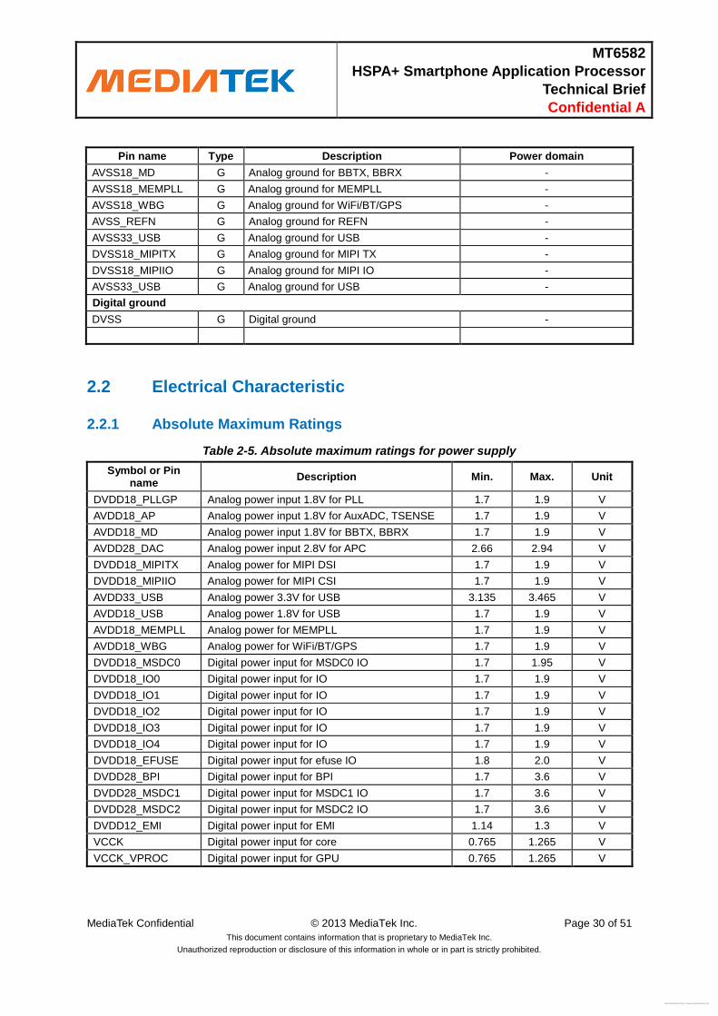
[email protected],time=2013-08-10 09:29:21,ip=112.90.37.152,doctitle=MT6582WG_Technical_Brief_v1.1.docx,company=Hexing_WCX
MT6582
HSPA+ Smartphone Application Processor
Technical Brief
Confidential A
MediaTek Confidential © 2013 MediaTek Inc. Page 30 of 51
This document contains information that is proprietary to MediaTek Inc.
Unauthorized reproduction or disclosure of this information in whole or in part is strictly prohibited.
Pin name Type Description Power domain
AVSS18_MD G Analog ground for BBTX, BBRX -
AVSS18_MEMPLL G Analog ground for MEMPLL -
AVSS18_WBG G Analog ground for WiFi/BT/GPS -
AVSS_REFN G Analog ground for REFN -
AVSS33_USB G Analog ground for USB -
DVSS18_MIPITX G Analog ground for MIPI TX -
DVSS18_MIPIIO G Analog ground for MIPI IO -
AVSS33_USB G Analog ground for USB -
Digital ground
DVSS G Digital ground -
2.2 Electrical Characteristic
2.2.1 Absolute Maximum Ratings
Table 2-5. Absolute maximum ratings for power supply
Symbol or Pin name
Description Min. Max. Unit
DVDD18_PLLGP Analog power input 1.8V for PLL 1.7 1.9 V
AVDD18_AP Analog power input 1.8V for AuxADC, TSENSE 1.7 1.9 V
AVDD18_MD Analog power input 1.8V for BBTX, BBRX 1.7 1.9 V
AVDD28_DAC Analog power input 2.8V for APC 2.66 2.94 V
DVDD18_MIPITX Analog power for MIPI DSI 1.7 1.9 V
DVDD18_MIPIIO Analog power for MIPI CSI 1.7 1.9 V
AVDD33_USB Analog power 3.3V for USB 3.135 3.465 V
AVDD18_USB Analog power 1.8V for USB 1.7 1.9 V
AVDD18_MEMPLL Analog power for MEMPLL 1.7 1.9 V
AVDD18_WBG Analog power for WiFi/BT/GPS 1.7 1.9 V
DVDD18_MSDC0 Digital power input for MSDC0 IO 1.7 1.95 V
DVDD18_IO0 Digital power input for IO 1.7 1.9 V
DVDD18_IO1 Digital power input for IO 1.7 1.9 V
DVDD18_IO2 Digital power input for IO 1.7 1.9 V
DVDD18_IO3 Digital power input for IO 1.7 1.9 V
DVDD18_IO4 Digital power input for IO 1.7 1.9 V
DVDD18_EFUSE Digital power input for efuse IO 1.8 2.0 V
DVDD28_BPI Digital power input for BPI 1.7 3.6 V
DVDD28_MSDC1 Digital power input for MSDC1 IO 1.7 3.6 V
DVDD28_MSDC2 Digital power input for MSDC2 IO 1.7 3.6 V
DVDD12_EMI Digital power input for EMI 1.14 1.3 V
VCCK Digital power input for core 0.765 1.265 V
VCCK_VPROC Digital power input for GPU 0.765 1.265 V
Free Datasheet http://www.nDatasheet.com
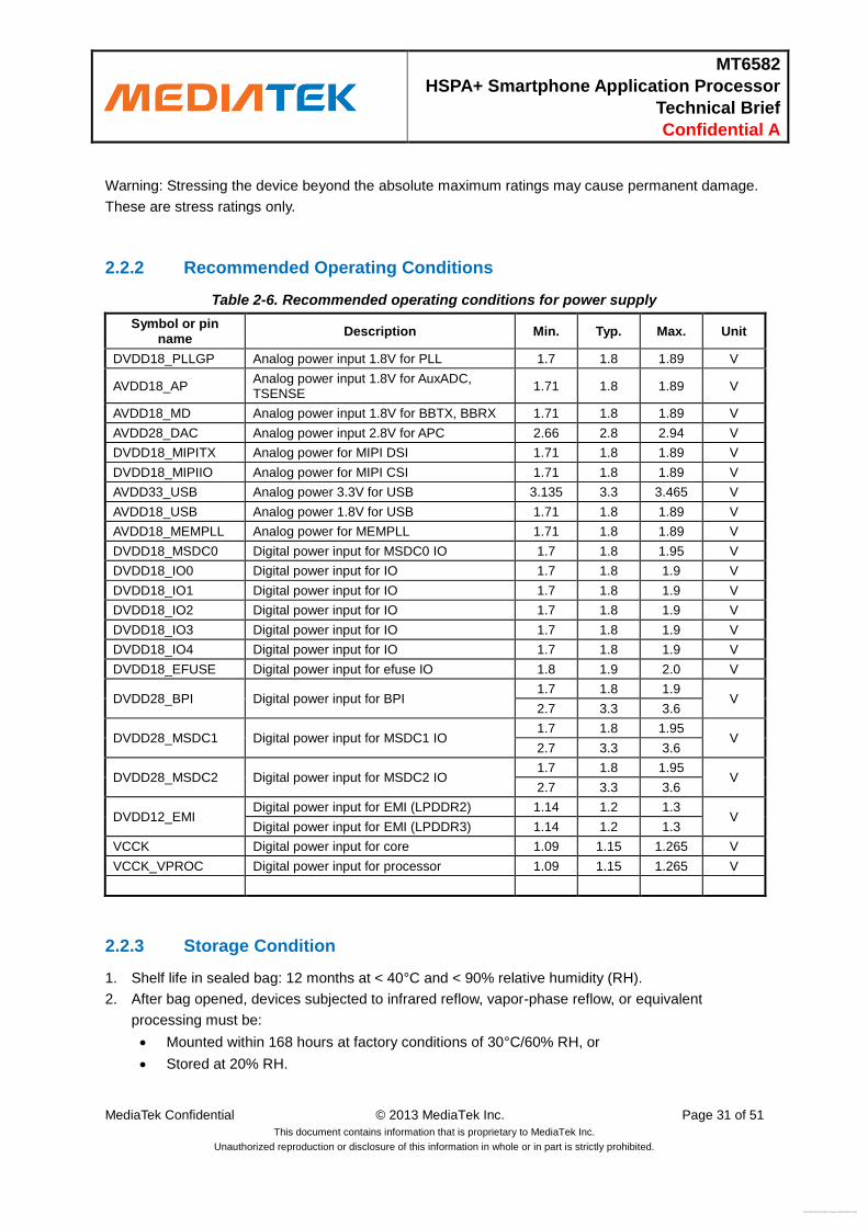
[email protected],time=2013-08-10 09:29:21,ip=112.90.37.152,doctitle=MT6582WG_Technical_Brief_v1.1.docx,company=Hexing_WCX
MT6582
HSPA+ Smartphone Application Processor
Technical Brief
Confidential A
MediaTek Confidential © 2013 MediaTek Inc. Page 31 of 51
This document contains information that is proprietary to MediaTek Inc.
Unauthorized reproduction or disclosure of this information in whole or in part is strictly prohibited.
Warning: Stressing the device beyond the absolute maximum ratings may cause permanent damage.
These are stress ratings only.
2.2.2 Recommended Operating Conditions
Table 2-6. Recommended operating conditions for power supply
Symbol or pin name
Description Min. Typ. Max. Unit
DVDD18_PLLGP Analog power input 1.8V for PLL 1.7 1.8 1.89 V
AVDD18_AP Analog power input 1.8V for AuxADC, TSENSE
1.71 1.8 1.89 V
AVDD18_MD Analog power input 1.8V for BBTX, BBRX 1.71 1.8 1.89 V
AVDD28_DAC Analog power input 2.8V for APC 2.66 2.8 2.94 V
DVDD18_MIPITX Analog power for MIPI DSI 1.71 1.8 1.89 V
DVDD18_MIPIIO Analog power for MIPI CSI 1.71 1.8 1.89 V
AVDD33_USB Analog power 3.3V for USB 3.135 3.3 3.465 V
AVDD18_USB Analog power 1.8V for USB 1.71 1.8 1.89 V
AVDD18_MEMPLL Analog power for MEMPLL 1.71 1.8 1.89 V
DVDD18_MSDC0 Digital power input for MSDC0 IO 1.7 1.8 1.95 V
DVDD18_IO0 Digital power input for IO 1.7 1.8 1.9 V
DVDD18_IO1 Digital power input for IO 1.7 1.8 1.9 V
DVDD18_IO2 Digital power input for IO 1.7 1.8 1.9 V
DVDD18_IO3 Digital power input for IO 1.7 1.8 1.9 V
DVDD18_IO4 Digital power input for IO 1.7 1.8 1.9 V
DVDD18_EFUSE Digital power input for efuse IO 1.8 1.9 2.0 V
DVDD28_BPI Digital power input for BPI 1.7 1.8 1.9
V 2.7 3.3 3.6
DVDD28_MSDC1 Digital power input for MSDC1 IO 1.7 1.8 1.95
V 2.7 3.3 3.6
DVDD28_MSDC2 Digital power input for MSDC2 IO 1.7 1.8 1.95
V 2.7 3.3 3.6
DVDD12_EMI Digital power input for EMI (LPDDR2) 1.14 1.2 1.3
V Digital power input for EMI (LPDDR3) 1.14 1.2 1.3
VCCK Digital power input for core 1.09 1.15 1.265 V
VCCK_VPROC Digital power input for processor 1.09 1.15 1.265 V
2.2.3 Storage Condition
1. Shelf life in sealed bag: 12 months at < 40°C and < 90% relative humidity (RH).
2. After bag opened, devices subjected to infrared reflow, vapor-phase reflow, or equivalent
processing must be:
Mounted within 168 hours at factory conditions of 30°C/60% RH, or
Stored at 20% RH.
Free Datasheet http://www.nDatasheet.com
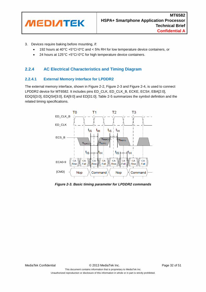
[email protected],time=2013-08-10 09:29:21,ip=112.90.37.152,doctitle=MT6582WG_Technical_Brief_v1.1.docx,company=Hexing_WCX
MT6582
HSPA+ Smartphone Application Processor
Technical Brief
Confidential A
MediaTek Confidential © 2013 MediaTek Inc. Page 32 of 51
This document contains information that is proprietary to MediaTek Inc.
Unauthorized reproduction or disclosure of this information in whole or in part is strictly prohibited.
3. Devices require baking before mounting, if:
192 hours at 40°C +5°C/-0°C and < 5% RH for low temperature device containers, or
24 hours at 125°C +5°C/-0°C for high temperature device containers.
2.2.4 AC Electrical Characteristics and Timing Diagram
2.2.4.1 External Memory Interface for LPDDR2
The external memory interface, shown in Figure 2-2, Figure 2-3 and Figure 2-4, is used to connect
LPDDR2 device for MT6582. It includes pins ED_CLK, ED_CLK_B, ECKE, ECS#, EBA[2:0],
EDQS[3:0], EDQS#[3:0], EA[9:0] and ED[31:0]. Table 2-5 summarizes the symbol definition and the
related timing specifications.
Figure 2-3. Basic timing parameter for LPDDR2 commands
ED_CLK
ED_CLK_B
ECS_B
ECA0-9
[CMD]
Free Datasheet http://www.nDatasheet.com
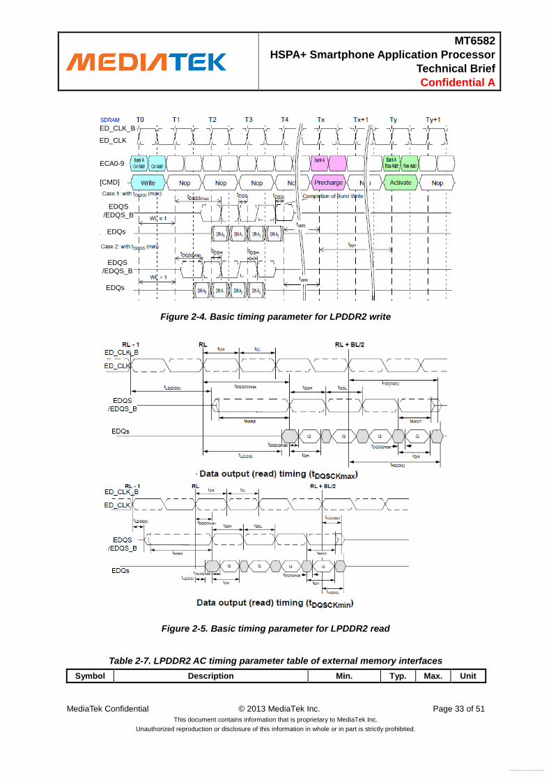
[email protected],time=2013-08-10 09:29:21,ip=112.90.37.152,doctitle=MT6582WG_Technical_Brief_v1.1.docx,company=Hexing_WCX
MT6582
HSPA+ Smartphone Application Processor
Technical Brief
Confidential A
MediaTek Confidential © 2013 MediaTek Inc. Page 33 of 51
This document contains information that is proprietary to MediaTek Inc.
Unauthorized reproduction or disclosure of this information in whole or in part is strictly prohibited.
Figure 2-4. Basic timing parameter for LPDDR2 write
Figure 2-5. Basic timing parameter for LPDDR2 read
Table 2-7. LPDDR2 AC timing parameter table of external memory interfaces
Symbol Description Min. Typ. Max. Unit
ED_CLK
ED_CLK_B
ECA0-9
[CMD]
EDQS
/EDQS_B
EDQs
EDQS
/EDQS_B
EDQs
Free Datasheet http://www.nDatasheet.com
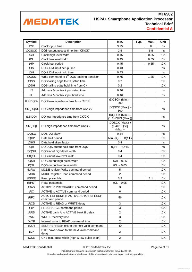
[email protected],time=2013-08-10 09:29:21,ip=112.90.37.152,doctitle=MT6582WG_Technical_Brief_v1.1.docx,company=Hexing_WCX
MT6582
HSPA+ Smartphone Application Processor
Technical Brief
Confidential A
MediaTek Confidential © 2013 MediaTek Inc. Page 34 of 51
This document contains information that is proprietary to MediaTek Inc.
Unauthorized reproduction or disclosure of this information in whole or in part is strictly prohibited.
Symbol Description Min. Typ. Max. Unit
tCK Clock cycle time 3.75
8 ns
tDQSCK DQS output access time from CK/CK’ 2.5
5.5 ns
tCH Clock high level width 0.45
0.55 tCK
tCL Clock low level width 0.45
0.55 tCK
tHP Clock half period 0.45
0.55 tCK
tDS DQ & DM input setup time 0.43
ns
tDH DQ & DM input hold time 0.43
ns
tDQSS Write command to 1st DQS latching transition 0.75
1.25 tCK
tDSS DQS falling edge to CK setup time 0.2
tCK
tDSH DQS falling edge hold time from CK 0.2
tCK
tIS Address & control input setup time 0.46
ns
tIH Address & control input hold time 0.46
ns
tLZ(DQS) DQS low-impedance time from CK/CK’ tDQSCK (Min.) –
300 ns
tHZ(DQS) DQS high-impedance time from CK/CK’ tDQSCK (Max.) –
100 ns
tLZ(DQ) DQ low-impedance time from CK/CK’ tDQSCK (Min.) –
(1.4×tQHS (Max.)) ns
tHZ(DQ) DQ high-impedance time from CK/CK’ tDQSCK (Max.) +
(1.4×tDQSQ (Max.))
ns
tDQSQ DQS-DQ skew 0.34
ns
tQHP Data half period Min. (tQSH, tQSL)
tCK
tQHS Data hold skew factor 0.4
ns
tQH DQ/DQS output hold time from DQS tQHP – tQHS
ns
tDQSH DQS input high-level width 0.4
tCK
tDQSL DQS input low-level width 0.4
tCK
tQSH DQS output high pulse width tCH – 0.05
tCK
tQSL DQS output low pulse width tCL – 0.05
tCK
tMRW MODE register Write command period 5
tCK
tMRR MODE register Read command period 2
tCK
tRPRE Read preamble 0.9
1.1 tCK
tRPST Read postamble tCL – 0.05
tCK
tRAS ACTIVE to PRECHARGE command period 3
tCK
tRC ACTIVE to ACTIVE command period 6
tCK
tRFC AUTO REFRESH to ACTIVE/AUTO REFRESH command period
56
tCK
tRCD ACTIVE to READ or WRITE delay 3
tCK
tRP PRECHARGE command period 3
tCK
tRRD ACTIVE bank A to ACTIVE bank B delay 2
tCK
tWR WRITE recovery time 3
tCK
tWTR Internal write to READ command time 2
tCK
tXSR SELF REFRESH exit to the next valid command 40
tCK
tXP EXIT power-down to the next valid command delay
2
tCK
tCKE CKE min. pulse width (high & low pulse width) 2
tCK
Free Datasheet http://www.nDatasheet.com
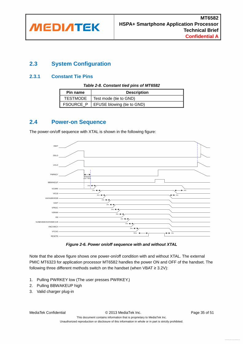
[email protected],time=2013-08-10 09:29:21,ip=112.90.37.152,doctitle=MT6582WG_Technical_Brief_v1.1.docx,company=Hexing_WCX
MT6582
HSPA+ Smartphone Application Processor
Technical Brief
Confidential A
MediaTek Confidential © 2013 MediaTek Inc. Page 35 of 51
This document contains information that is proprietary to MediaTek Inc.
Unauthorized reproduction or disclosure of this information in whole or in part is strictly prohibited.
2.3 System Configuration
2.3.1 Constant Tie Pins
Table 2-8. Constant tied pins of MT6582
Pin name Description TESTMODE Test mode (tie to GND) FSOURCE_P EFUSE blowing (tie to GND)
2.4 Power-on Sequence
The power-on/off sequence with XTAL is shown in the following figure:
VBAT
DDLO
UVLO
PWRKEY
BBWAKEUP
VCORE
VIO18
VA/VA28/VIO28
VAST
VPROC
VSRAM
VM
VUSB/VEMC3V3/VEMC1V8
VMC/VMCH
VTCXO
RESETB
De-bounce
time = 50ms
2ms
2ms
2ms
2ms
2ms
2ms
2ms
2ms
2ms
2ms
20ms
2ms
8ms
2ms
Figure 2-6. Power on/off sequence with and without XTAL
Note that the above figure shows one power-on/off condition with and without XTAL. The external
PMIC MT6323 for application processor MT6582 handles the power ON and OFF of the handset. The
following three different methods switch on the handset (when VBAT ≥ 3.2V):
1. Pulling PWRKEY low (The user presses PWRKEY.)
2. Pulling BBWAKEUP high
3. Valid charger plug-in
Free Datasheet http://www.nDatasheet.com
[email protected],time=2013-08-10 09:29:21,ip=112.90.37.152,doctitle=MT6582WG_Technical_Brief_v1.1.docx,company=Hexing_WCX
MT6582
HSPA+ Smartphone Application Processor
Technical Brief
Confidential A
MediaTek Confidential © 2013 MediaTek Inc. Page 36 of 51
This document contains information that is proprietary to MediaTek Inc.
Unauthorized reproduction or disclosure of this information in whole or in part is strictly prohibited.
Pulling PWRKEY low is a normal way to turn on the handset, which turns on regulators as long as the
PWRKEY is kept low. MT6323 outputs reset signal RESETB to MT6582 SYSRSTB input. After
SYSRSTB is de-asserted, the microprocessor starts and pulls BBWAKEUP high. After that PWRKEY
can be released, pulling BBWAKEUP high will also turn on the handset. This is the case when the
alarm in the RTC expires.
Besides, applying a valid external supply on CHRIN will also turn on the handset. However, if the
battery is in the UV state (VBAT < 3.2V), the handset cannot be turned on in any way.
The UVLO function in MT6323 prevents system startup when initial voltage of the main battery is
below the 3.2V threshold. When the battery voltage is bigger than 3.2V, the UVLO comparator
switches and threshold are reduced to 2.75V, which allows the handset to start smoothly unless the
battery decays to 2.75V and below.
Once MT6323 enters the UVLO state, it draws very low quiescent current. The VRTC LDO will still be
active until the DDLO disables it.
The timing diagram also shows the power-on/off sequence without XTAL. VTCXO is always turned on
when VBAT is above the DDLO threshold.
2.5 Analog Baseband
2.5.1 Introduction
To communicate with analog blocks, a common control interface for all analog blocks is implemented.
In addition, there are some dedicated interfaces for data transfer. The common control interface
translates the APB bus write and read cycle for specific addresses related to analog front-end control.
During the writing or reading of any of these control registers, there is a latency associated with the
transfer of data to or from the analog front-end. Dedicated data interface of each analog block is
implemented in the corresponding digital block. An analog block includes the following analog
functions for the complete GSM/GPRS/WCDMA base-band signal processing:
Base-band Rx: For I/Q channels base-band A/D conversion
Base-band Tx: For I/Q channels base-band D/A conversion and smoothing filtering
RF control: One DAC for automatic power control (APC) is included. The output is provided to the
external RF power amplifier respectively. One more DAC for voltage bias control (VBIAS) is
included for WCDMA system, and the output is provided to the external RF power amplifier.
Auxiliary ADC: Provides an ADC for the battery and other auxiliary analog functions monitoring.
Clock generation: One clock-squarer for shaping the input sinwave clock and 10 PLLs providing
clock signals to base-band TRx, DSP, MCU, USB, MSDC units.
Free Datasheet http://www.nDatasheet.com
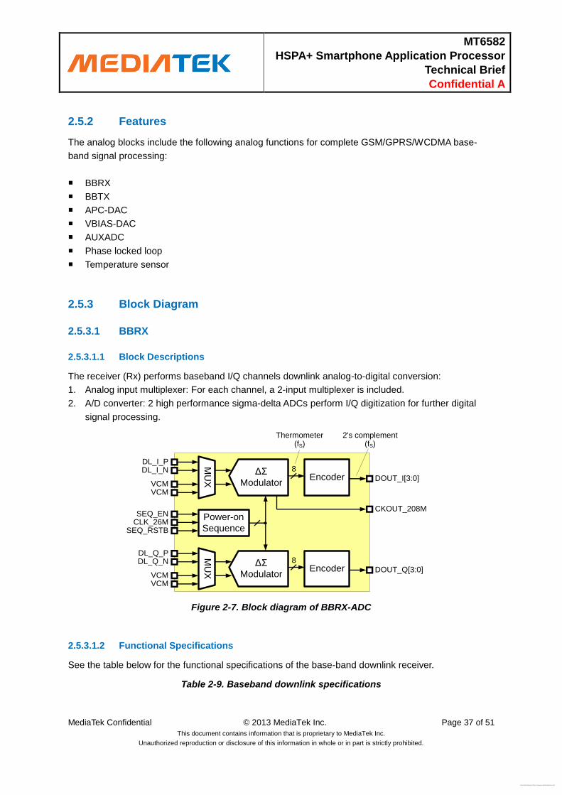
[email protected],time=2013-08-10 09:29:21,ip=112.90.37.152,doctitle=MT6582WG_Technical_Brief_v1.1.docx,company=Hexing_WCX
MT6582
HSPA+ Smartphone Application Processor
Technical Brief
Confidential A
MediaTek Confidential © 2013 MediaTek Inc. Page 37 of 51
This document contains information that is proprietary to MediaTek Inc.
Unauthorized reproduction or disclosure of this information in whole or in part is strictly prohibited.
2.5.2 Features
The analog blocks include the following analog functions for complete GSM/GPRS/WCDMA base-
band signal processing:
BBRX
BBTX
APC-DAC
VBIAS-DAC
AUXADC
Phase locked loop
Temperature sensor
2.5.3 Block Diagram
2.5.3.1 BBRX
2.5.3.1.1 Block Descriptions
The receiver (Rx) performs baseband I/Q channels downlink analog-to-digital conversion:
1. Analog input multiplexer: For each channel, a 2-input multiplexer is included.
2. A/D converter: 2 high performance sigma-delta ADCs perform I/Q digitization for further digital
signal processing.
DL_I_PDL_I_N
VCMVCM
MU
X
ΔΣ
ModulatorEncoder
8
Thermometer (fS)
DOUT_I[3:0]
2's complement(fS)
DL_Q_PDL_Q_N
VCMVCM
MU
X
ΔΣ
ModulatorEncoder
8
DOUT_Q[3:0]
CKOUT_208MPower-on
Sequence
SEQ_ENCLK_26M
SEQ_RSTB
Figure 2-7. Block diagram of BBRX-ADC
2.5.3.1.2 Functional Specifications
See the table below for the functional specifications of the base-band downlink receiver.
Table 2-9. Baseband downlink specifications
Free Datasheet http://www.nDatasheet.com
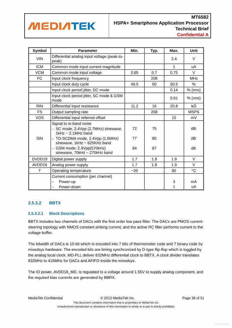
[email protected],time=2013-08-10 09:29:21,ip=112.90.37.152,doctitle=MT6582WG_Technical_Brief_v1.1.docx,company=Hexing_WCX
MT6582
HSPA+ Smartphone Application Processor
Technical Brief
Confidential A
MediaTek Confidential © 2013 MediaTek Inc. Page 38 of 51
This document contains information that is proprietary to MediaTek Inc.
Unauthorized reproduction or disclosure of this information in whole or in part is strictly prohibited.
Symbol Parameter Min. Typ. Max. Unit
VIN Differential analog input voltage (peak-to-peak) 2.4 V
ICM Common mode input current magnitude 1 uA
VCM Common mode input voltage 0.65 0.7 0.75 V
FC Input clock frequency 208 MHz
Input clock duty cycle 49.5 50 50.5 %
Input clock period jitter, DC mode 0.14 % (rms)
Input clock period jitter, SC mode & GSM mode
0.61 % (rms)
RIN Differential input resistance 11.2 16 20.8 kΩ
FS Output sampling rate 208 MSPS
VOS Differential input referred offset 10 mV
SIN
Signal to in-band noise
SC mode, 2.4Vpp (2.7MHz) sinewave, 1kHz ~ 2.1MHz band
TD-SCDMA mode, 2.4Vpp (1.6MHz) sinewave, 1kHz ~ 625KHz band
GSM mode: 2.4Vpp(570kHz) sinewave, 70kHz ~ 270kHz band
72
77
84
75
80
87
dB
dB
dB
DVDD18 Digital power supply 1.7 1.8 1.9 V
AVDD18 Analog power supply 1.7 1.8 1.9 V
T Operating temperature −20 80 °C
Current consumption (per channel)
Power-up
Power-down
3
1
mA uA
2.5.3.2 BBTX
2.5.3.2.1 Block Descriptions
BBTX includes two channels of DACs with the first order low pass filter. The DACs are PMOS current-
steering topology with NMOS constant sinking current, and the active RC filter performs current to the
voltage buffer.
The bitwidth of DACs is 10-bit which is encoded into 7 bits of thermometer code and 7 binary code by
mixedsys hardware. The encoded bits are timing synchronized by D-type flip-flop which is toggled by
the analog local clock. MD-PLL deliver 832MHz differential clock to BBTX. A clock divider translates
832MHz to 416MHz for DACs and AFIFO inside the mixedsys.
The IO power, AVDD18_MD, is regulated to a voltage around 1.55V to supply analog component, and
the required bias currents are generated by BBRX.
Free Datasheet http://www.nDatasheet.com
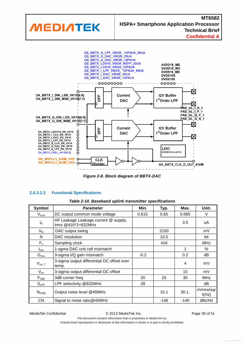
[email protected],time=2013-08-10 09:29:21,ip=112.90.37.152,doctitle=MT6582WG_Technical_Brief_v1.1.docx,company=Hexing_WCX
MT6582
HSPA+ Smartphone Application Processor
Technical Brief
Confidential A
MediaTek Confidential © 2013 MediaTek Inc. Page 39 of 51
This document contains information that is proprietary to MediaTek Inc.
Unauthorized reproduction or disclosure of this information in whole or in part is strictly prohibited.
Figure 2-8. Block diagram of BBTX-DAC
2.5.3.2.2 Functional Specifications
Table 2-10. Baseband uplink transmitter specifications
Symbol Parameter Min. Typ. Max. Unit. Vocm DC output common mode voltage 0.615 0.65 0.685 V
IK HF Leakage Leakage current @ supply, Irms @416*2=832MHz
3.5 uA
Vfs DAC output swing 2100 mV
N DAC resolution 10.0 bit
Fs Sampling clock 416 MHz
Imis 1-sgma DAC unit cell mismatch
1 %
Gmis 3-sigma I/Q gain mismatch -0.2
0.2 dB
Vos_T 3-sigma output differential DC offset over temp.
4 mV
Vos 3-sigma output differential DC offset
10 mV
F3dB 3dB corner freq. 20 25 30 MHz
SLPF LPF selectivity @832MHz 28
dB
NOOB Output noise level @45MHz 15.1 30.1. nVrms/sqr
t(Hz)
CN Signal to noise ratio@45MHz -146 -140 dBc/Hz
Free Datasheet http://www.nDatasheet.com
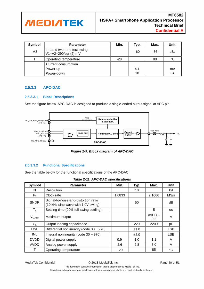
[email protected],time=2013-08-10 09:29:21,ip=112.90.37.152,doctitle=MT6582WG_Technical_Brief_v1.1.docx,company=Hexing_WCX
MT6582
HSPA+ Smartphone Application Processor
Technical Brief
Confidential A
MediaTek Confidential © 2013 MediaTek Inc. Page 40 of 51
This document contains information that is proprietary to MediaTek Inc.
Unauthorized reproduction or disclosure of this information in whole or in part is strictly prohibited.
Symbol Parameter Min. Typ. Max. Unit.
IM3 In-band two-tone test swing V1=V2=290/sqrt(2) mV
-60 -56 dBc
T Operating temperature -20 80 °C
Current consumption
Power-up
Power-down
4.1
10
mA
uA
2.5.3.3 APC-DAC
2.5.3.3.1 Block Descriptions
See the figure below. APC-DAC is designed to produce a single-ended output signal at APC pin.
Figure 2-9. Block diagram of APC-DAC
2.5.3.3.2 Functional Specifications
See the table below for the functional specifications of the APC-DAC.
Table 2-11. APC-DAC specifications
Symbol Parameter Min. Typ. Max. Unit N Resolution 10 Bit
FS Clock rate 1.0833 2.1666 MS/s
SNDR Signal-to-noise-and-distortion ratio
(10 kHz sine wave with 1.0V swing) 50 dB
TS Settling time (99% full-swing settling) 5 us
VO,max Maximum output AVDD
0.2 V
CL Output loading capacitance 220 2200 pF
DNL Differential nonlinearity (code 30 ~ 970) 1.0 LSB
INL Integral nonlinearity (code 30 ~ 970) 2.0 LSB
DVDD Digital power supply 0.9 1.0 1.1 V
AVDD Analog power supply 2.6 2.8 3.0 V
T Operating temperature 20 85 C
Reference buffer& bias gen.
R-string DAC core10- bit DFF
APC-DAC
APC_EN
Output
Buffer
PAD_APCAPC_BUS[9:0]
APC_RSTB
RG_APC_TGSEL
APC_TG
VBG(from bandgap)RG_APCBUF_TRIM[3:0]
PA
Free Datasheet http://www.nDatasheet.com
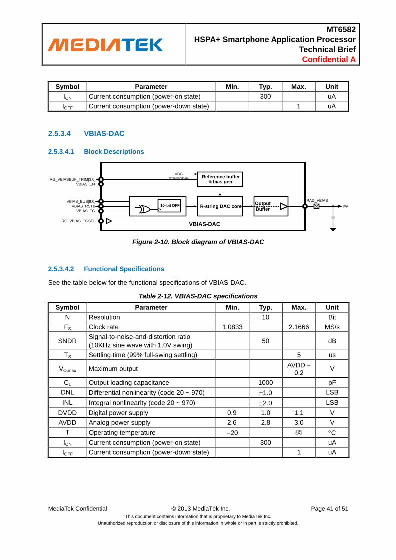
[email protected],time=2013-08-10 09:29:21,ip=112.90.37.152,doctitle=MT6582WG_Technical_Brief_v1.1.docx,company=Hexing_WCX
MT6582
HSPA+ Smartphone Application Processor
Technical Brief
Confidential A
MediaTek Confidential © 2013 MediaTek Inc. Page 41 of 51
This document contains information that is proprietary to MediaTek Inc.
Unauthorized reproduction or disclosure of this information in whole or in part is strictly prohibited.
Symbol Parameter Min. Typ. Max. Unit ION Current consumption (power-on state) 300 uA
IOFF Current consumption (power-down state) 1 uA
2.5.3.4 VBIAS-DAC
2.5.3.4.1 Block Descriptions
Figure 2-10. Block diagram of VBIAS-DAC
2.5.3.4.2 Functional Specifications
See the table below for the functional specifications of VBIAS-DAC.
Table 2-12. VBIAS-DAC specifications
Symbol Parameter Min. Typ. Max. Unit N Resolution 10 Bit
FS Clock rate 1.0833 2.1666 MS/s
SNDR Signal-to-noise-and-distortion ratio
(10KHz sine wave with 1.0V swing) 50 dB
TS Settling time (99% full-swing settling) 5 us
VO,max Maximum output AVDD
0.2 V
CL Output loading capacitance 1000 pF
DNL Differential nonlinearity (code 20 ~ 970) 1.0 LSB
INL Integral nonlinearity (code 20 ~ 970) 2.0 LSB
DVDD Digital power supply 0.9 1.0 1.1 V
AVDD Analog power supply 2.6 2.8 3.0 V
T Operating temperature 20 85 C
ION Current consumption (power-on state) 300 uA
IOFF Current consumption (power-down state) 1 uA
Reference buffer& bias gen.
R-string DAC core10- bit DFF
VBIAS-DAC
VBIAS_EN
Output
Buffer
PAD_VBIASVBIAS_BUS[9:0]
VBIAS_RSTB
RG_VBIAS_TGSEL
VBIAS_TG
VBG(from bandgap)RG_VBIASBUF_TRIM[3:0]
PA
Free Datasheet http://www.nDatasheet.com
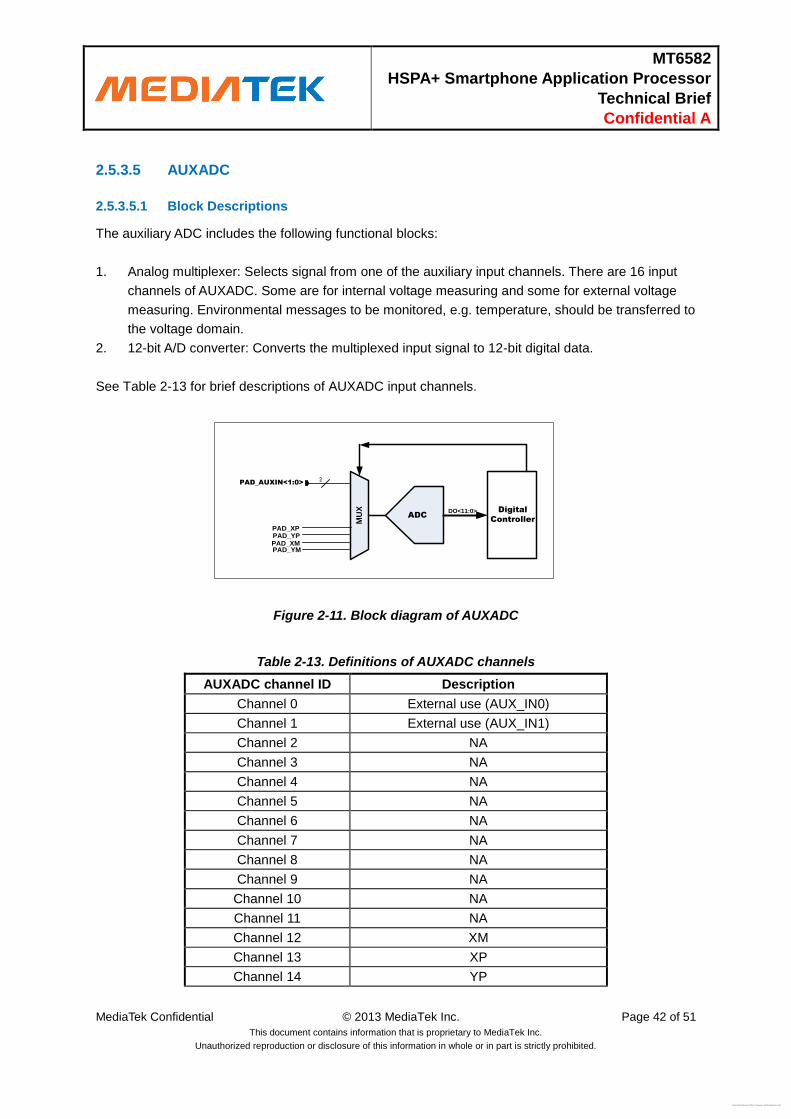
[email protected],time=2013-08-10 09:29:21,ip=112.90.37.152,doctitle=MT6582WG_Technical_Brief_v1.1.docx,company=Hexing_WCX
MT6582
HSPA+ Smartphone Application Processor
Technical Brief
Confidential A
MediaTek Confidential © 2013 MediaTek Inc. Page 42 of 51
This document contains information that is proprietary to MediaTek Inc.
Unauthorized reproduction or disclosure of this information in whole or in part is strictly prohibited.
2.5.3.5 AUXADC
2.5.3.5.1 Block Descriptions
The auxiliary ADC includes the following functional blocks:
1. Analog multiplexer: Selects signal from one of the auxiliary input channels. There are 16 input
channels of AUXADC. Some are for internal voltage measuring and some for external voltage
measuring. Environmental messages to be monitored, e.g. temperature, should be transferred to
the voltage domain.
2. 12-bit A/D converter: Converts the multiplexed input signal to 12-bit digital data.
See Table 2-13 for brief descriptions of AUXADC input channels.
PAD_AUXIN<1:0>2
MU
X
ADC
Digital
Controller
DO<11:0>
PAD_XPPAD_YP
PAD_YMPAD_XM
Figure 2-11. Block diagram of AUXADC
Table 2-13. Definitions of AUXADC channels
AUXADC channel ID Description Channel 0 External use (AUX_IN0) Channel 1 External use (AUX_IN1) Channel 2 NA Channel 3 NA Channel 4 NA Channel 5 NA Channel 6 NA Channel 7 NA Channel 8 NA Channel 9 NA Channel 10 NA Channel 11 NA Channel 12 XM Channel 13 XP Channel 14 YP
Free Datasheet http://www.nDatasheet.com
[email protected],time=2013-08-10 09:29:21,ip=112.90.37.152,doctitle=MT6582WG_Technical_Brief_v1.1.docx,company=Hexing_WCX
MT6582
HSPA+ Smartphone Application Processor
Technical Brief
Confidential A
MediaTek Confidential © 2013 MediaTek Inc. Page 43 of 51
This document contains information that is proprietary to MediaTek Inc.
Unauthorized reproduction or disclosure of this information in whole or in part is strictly prohibited.
AUXADC channel ID Description Channel 15 YM
2.5.3.5.2 Functional Specifications
See the table below for the functional specifications of auxiliary ADC.
Table 2-14. AUXADC specifications
Symbol Parameter Min. Typ. Max. Unit N Resolution 12 Bit
FC Clock rate 4 MHz
FS Sampling rate @ N-Bit 4/(N+4) MSPS
Input swing 0.05 1.45 V
CIN
Input capacitance
Unselected channel
Selected channel
50
4
fF
pF
RIN Input resistance
Unselected channel
400
MΩ
Clock latency N+4 1/FC
DNL Differential nonlinearity +1.0/-1.0 LSB
INL Integral nonlinearity +2.0/-2.0 LSB
SINAD Signal to noise and distortion ratio (1kHz full swing input & 1.0833MHz clock rate)
62 68 dB
DVDD Digital power supply 1.0 1.1 1.2 V
AVDD Analog power supply 1.75 1.8 1.85 V
T Operating temperature -20 80 °C
Current consumption
Power-up
Power-down
400
1
uA
uA
2.5.3.6 Clock Squarer
2.5.3.6.1 Block Descriptions
For most VCXO, the output clock waveform is sinusoidal with too small amplitude (about several
hundred mV) to make MT6582 digital circuits function well. The clock squarer is designed to convert
such a small signal to a rail-to-rail clock signal with excellent duty-cycle.
2.5.3.6.2 Functional Specifications
See the table below for the functional specifications of clock squarer.
Table 2-15. Clock squarer specifications
Free Datasheet http://www.nDatasheet.com
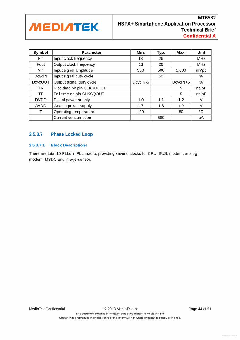
[email protected],time=2013-08-10 09:29:21,ip=112.90.37.152,doctitle=MT6582WG_Technical_Brief_v1.1.docx,company=Hexing_WCX
MT6582
HSPA+ Smartphone Application Processor
Technical Brief
Confidential A
MediaTek Confidential © 2013 MediaTek Inc. Page 44 of 51
This document contains information that is proprietary to MediaTek Inc.
Unauthorized reproduction or disclosure of this information in whole or in part is strictly prohibited.
Symbol Parameter Min. Typ. Max. Unit Fin Input clock frequency 13 26 MHz
Fout Output clock frequency 13 26 MHz
Vin Input signal amplitude 350 500 1,000 mVpp
DcycIN Input signal duty cycle 50 %
DcycOUT Output signal duty cycle DcycIN-5 DcycIN+5 %
TR Rise time on pin CLKSQOUT 5 ns/pF
TF Fall time on pin CLKSQOUT 5 ns/pF
DVDD Digital power supply 1.0 1.1 1.2 V
AVDD Analog power supply 1.7 1.8 1.9 V
T Operating temperature -20 80 °C
Current consumption 500 uA
2.5.3.7 Phase Locked Loop
2.5.3.7.1 Block Descriptions
There are total 10 PLLs in PLL macro, providing several clocks for CPU, BUS, modem, analog
modem, MSDC and image-sensor.
Free Datasheet http://www.nDatasheet.com
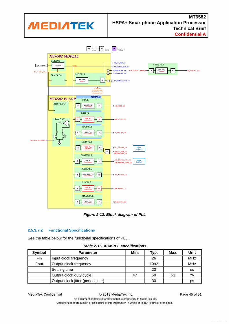
[email protected],time=2013-08-10 09:29:21,ip=112.90.37.152,doctitle=MT6582WG_Technical_Brief_v1.1.docx,company=Hexing_WCX
MT6582
HSPA+ Smartphone Application Processor
Technical Brief
Confidential A
MediaTek Confidential © 2013 MediaTek Inc. Page 45 of 51
This document contains information that is proprietary to MediaTek Inc.
Unauthorized reproduction or disclosure of this information in whole or in part is strictly prohibited.
CLKSQ
CLKSQ1
Bias / LDO
26MHzPAD_CLK26M_1
AD_MEM_26M_CK
AD_MIPI_26M_CK
AD_MDSYS1_26M_CK
MDPLL1
MD_PLL(832MHz) AD_MDPLL1_416M_CK/2
MT6582 MDPLL1
RG_CLKSQ1_EN
To BBTRXNS_MD832M_CKP
NS_MD832M_CKN
QS_MD832M_VSS
WPLL
AD_WPLL_CK
MCUPLL
WHPLL
AD_WHPLL_CK
WSDM_PLL(1966.08MHz)
SDM_PLL(Hop 1001MHz)
SDM_PLL(Hop 1924MHz)
/M /MExternal
of PLLInternal
of PLL
/M Analog Special
Divider
/4
/2
/4
UNIVPLL
SDM_PLL(1248MHz)
MAINPLL
ARMPLL
AD_ARMPLL_CK
SDM_PLL(Hop 1092MHz)
ARM_SDM_PLL(Hop 1092MHz)
SDM_PLL(Hop 1001MHz)
MMPLL
MSDCPLL
SDM_PLL(Hop 1664MHz)
/4
/1
MODEM
Test CKT
+
-
Bias / LDO
MT6582 PLLGP
/1
AD_SYS_26M_CK
DA_ARMCPU_MON_CK
/1
/1
/1
/1
/1
/1/1
/1
/1
/2
AD_MCUPLL_CK
AD_UNIVPLL_CK
AD_MAINPLL_PRO_CK
AD_MAINPLL_CORE_CK
AD_MMPLL_CK
AD_MSDCPLL_CK
/26 AD_USB_48M_CKAD_UNIV_48M_CK
VENCPLL
AD_VENCPLL_CKSDM_PLL
(1183MHz)/4/1ADA_VENCPLL_REFCLK
Digital
/2,/3,/5,/7
Digital
/2,/3,/5,/7
Figure 2-12. Block diagram of PLL
2.5.3.7.2 Functional Specifications
See the table below for the functional specifications of PLL.
Table 2-16. ARMPLL specifications
Symbol Parameter Min. Typ. Max. Unit Fin Input clock frequency 26 MHz
Fout Output clock frequency 1092 MHz
Settling time 20 us
Output clock duty cycle 47 50 53 %
Output clock jitter (period jitter) 30 ps
Free Datasheet http://www.nDatasheet.com
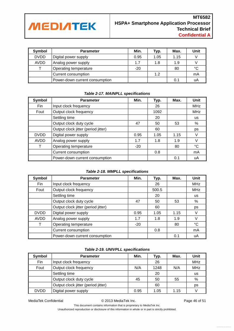
[email protected],time=2013-08-10 09:29:21,ip=112.90.37.152,doctitle=MT6582WG_Technical_Brief_v1.1.docx,company=Hexing_WCX
MT6582
HSPA+ Smartphone Application Processor
Technical Brief
Confidential A
MediaTek Confidential © 2013 MediaTek Inc. Page 46 of 51
This document contains information that is proprietary to MediaTek Inc.
Unauthorized reproduction or disclosure of this information in whole or in part is strictly prohibited.
Symbol Parameter Min. Typ. Max. Unit DVDD Digital power supply 0.95 1.05 1.15 V
AVDD Analog power supply 1.7 1.8 1.9 V
T Operating temperature -20 80 °C
Current consumption 1.2 mA
Power-down current consumption 0.1 uA
Table 2-17. MAINPLL specifications
Symbol Parameter Min. Typ. Max. Unit Fin Input clock frequency 26 MHz
Fout Output clock frequency 1092 MHz
Settling time 20 us
Output clock duty cycle 47 50 53 %
Output clock jitter (period jitter) 60 ps
DVDD Digital power supply 0.95 1.05 1.15 V
AVDD Analog power supply 1.7 1.8 1.9 V
T Operating temperature -20 80 °C
Current consumption 0.8 mA
Power-down current consumption 0.1 uA
Table 2-18. MMPLL specifications
Symbol Parameter Min. Typ. Max. Unit Fin Input clock frequency 26 MHz
Fout Output clock frequency 500.5 MHz
Settling time 20 us
Output clock duty cycle 47 50 53 %
Output clock jitter (period jitter) 60 ps
DVDD Digital power supply 0.95 1.05 1.15 V
AVDD Analog power supply 1.7 1.8 1.9 V
T Operating temperature -20 80 °C
Current consumption 0.8 mA
Power-down current consumption 0.1 uA
Table 2-19. UNIVPLL specifications
Symbol Parameter Min. Typ. Max. Unit Fin Input clock frequency 26 MHz
Fout Output clock frequency N/A 1248 N/A MHz
Settling time 20 us
Output clock duty cycle 45 50 55 %
Output clock jitter (period jitter) 60 ps
DVDD Digital power supply 0.95 1.05 1.15 V
Free Datasheet http://www.nDatasheet.com
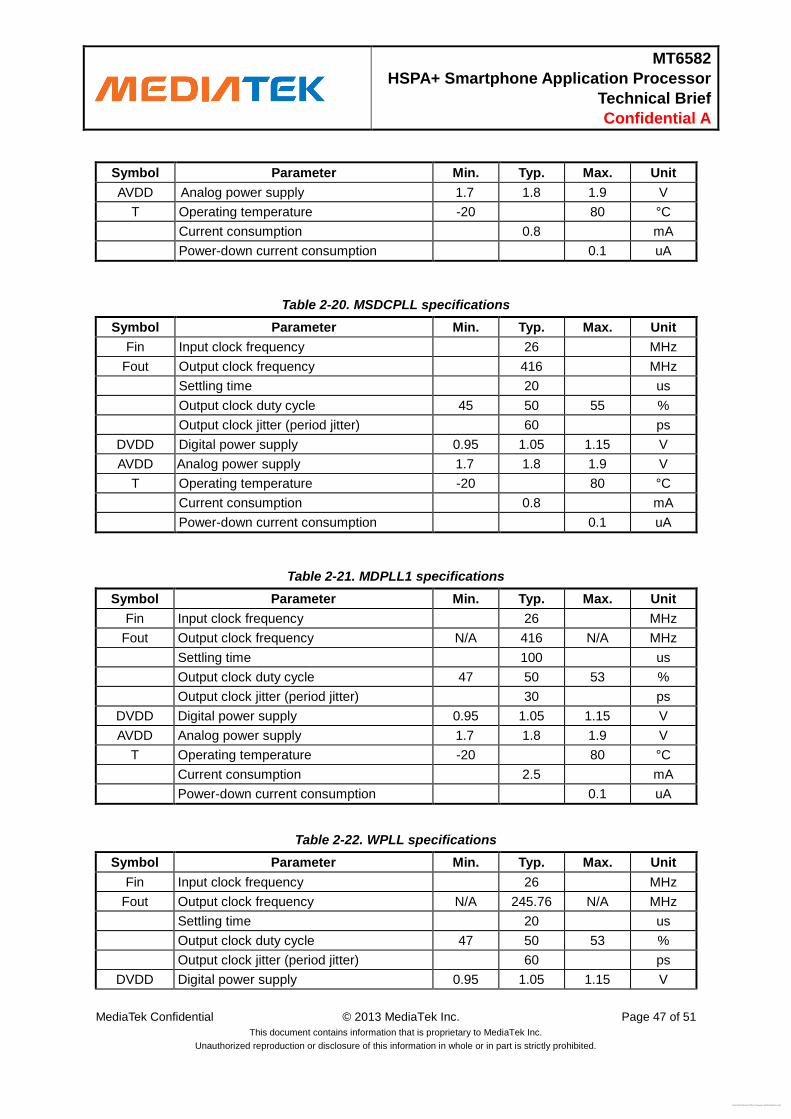
[email protected],time=2013-08-10 09:29:21,ip=112.90.37.152,doctitle=MT6582WG_Technical_Brief_v1.1.docx,company=Hexing_WCX
MT6582
HSPA+ Smartphone Application Processor
Technical Brief
Confidential A
MediaTek Confidential © 2013 MediaTek Inc. Page 47 of 51
This document contains information that is proprietary to MediaTek Inc.
Unauthorized reproduction or disclosure of this information in whole or in part is strictly prohibited.
Symbol Parameter Min. Typ. Max. Unit AVDD Analog power supply 1.7 1.8 1.9 V
T Operating temperature -20 80 °C
Current consumption 0.8 mA
Power-down current consumption 0.1 uA
Table 2-20. MSDCPLL specifications
Symbol Parameter Min. Typ. Max. Unit Fin Input clock frequency 26 MHz
Fout Output clock frequency 416 MHz
Settling time 20 us
Output clock duty cycle 45 50 55 %
Output clock jitter (period jitter) 60 ps
DVDD Digital power supply 0.95 1.05 1.15 V
AVDD Analog power supply 1.7 1.8 1.9 V
T Operating temperature -20 80 °C
Current consumption 0.8 mA
Power-down current consumption 0.1 uA
Table 2-21. MDPLL1 specifications
Symbol Parameter Min. Typ. Max. Unit Fin Input clock frequency 26 MHz
Fout Output clock frequency N/A 416 N/A MHz Settling time 100 us
Output clock duty cycle 47 50 53 %
Output clock jitter (period jitter) 30 ps
DVDD Digital power supply 0.95 1.05 1.15 V AVDD Analog power supply 1.7 1.8 1.9 V
T Operating temperature -20 80 °C
Current consumption 2.5 mA
Power-down current consumption 0.1 uA
Table 2-22. WPLL specifications
Symbol Parameter Min. Typ. Max. Unit Fin Input clock frequency 26 MHz
Fout Output clock frequency N/A 245.76 N/A MHz Settling time 20 us
Output clock duty cycle 47 50 53 %
Output clock jitter (period jitter) 60 ps
DVDD Digital power supply 0.95 1.05 1.15 V
Free Datasheet http://www.nDatasheet.com
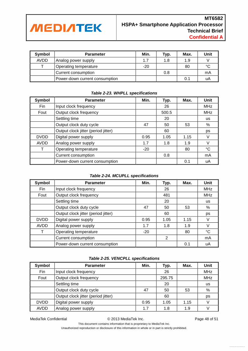
[email protected],time=2013-08-10 09:29:21,ip=112.90.37.152,doctitle=MT6582WG_Technical_Brief_v1.1.docx,company=Hexing_WCX
MT6582
HSPA+ Smartphone Application Processor
Technical Brief
Confidential A
MediaTek Confidential © 2013 MediaTek Inc. Page 48 of 51
This document contains information that is proprietary to MediaTek Inc.
Unauthorized reproduction or disclosure of this information in whole or in part is strictly prohibited.
Symbol Parameter Min. Typ. Max. Unit AVDD Analog power supply 1.7 1.8 1.9 V
T Operating temperature -20 80 °C
Current consumption 0.8 mA
Power-down current consumption 0.1 uA
Table 2-23. WHPLL specifications
Symbol Parameter Min. Typ. Max. Unit Fin Input clock frequency 26 MHz
Fout Output clock frequency 500.5 MHz
Settling time 20 us
Output clock duty cycle 47 50 53 %
Output clock jitter (period jitter) 60 ps
DVDD Digital power supply 0.95 1.05 1.15 V
AVDD Analog power supply 1.7 1.8 1.9 V
T Operating temperature -20 80 °C
Current consumption 0.8 mA
Power-down current consumption 0.1 uA
Table 2-24. MCUPLL specifications
Symbol Parameter Min. Typ. Max. Unit Fin Input clock frequency 26 MHz
Fout Output clock frequency 481 MHz
Settling time 20 us
Output clock duty cycle 47 50 53 %
Output clock jitter (period jitter) 60 ps
DVDD Digital power supply 0.95 1.05 1.15 V
AVDD Analog power supply 1.7 1.8 1.9 V
T Operating temperature -20 80 °C
Current consumption 2 mA
Power-down current consumption 0.1 uA
Table 2-25. VENCPLL specifications
Symbol Parameter Min. Typ. Max. Unit Fin Input clock frequency 26 MHz
Fout Output clock frequency 295.75 MHz
Settling time 20 us
Output clock duty cycle 47 50 53 %
Output clock jitter (period jitter) 60 ps
DVDD Digital power supply 0.95 1.05 1.15 V
AVDD Analog power supply 1.7 1.8 1.9 V
Free Datasheet http://www.nDatasheet.com
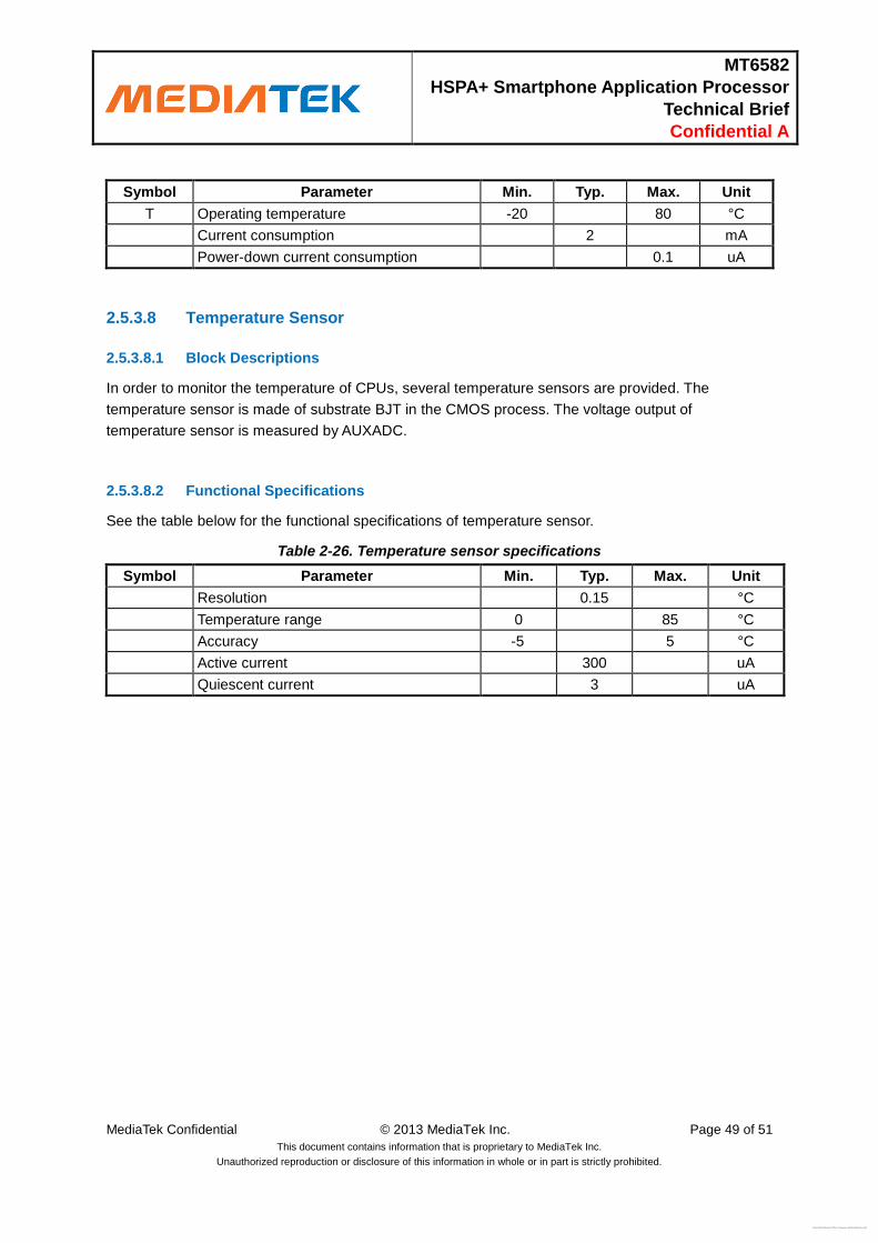
[email protected],time=2013-08-10 09:29:21,ip=112.90.37.152,doctitle=MT6582WG_Technical_Brief_v1.1.docx,company=Hexing_WCX
MT6582
HSPA+ Smartphone Application Processor
Technical Brief
Confidential A
MediaTek Confidential © 2013 MediaTek Inc. Page 49 of 51
This document contains information that is proprietary to MediaTek Inc.
Unauthorized reproduction or disclosure of this information in whole or in part is strictly prohibited.
Symbol Parameter Min. Typ. Max. Unit T Operating temperature -20 80 °C
Current consumption 2 mA
Power-down current consumption 0.1 uA
2.5.3.8 Temperature Sensor
2.5.3.8.1 Block Descriptions
In order to monitor the temperature of CPUs, several temperature sensors are provided. The
temperature sensor is made of substrate BJT in the CMOS process. The voltage output of
temperature sensor is measured by AUXADC.
2.5.3.8.2 Functional Specifications
See the table below for the functional specifications of temperature sensor.
Table 2-26. Temperature sensor specifications
Symbol Parameter Min. Typ. Max. Unit Resolution 0.15 °C
Temperature range 0 85 °C
Accuracy -5 5 °C
Active current 300 uA
Quiescent current 3 uA
Free Datasheet http://www.nDatasheet.com
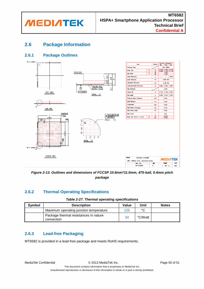
[email protected],time=2013-08-10 09:29:21,ip=112.90.37.152,doctitle=MT6582WG_Technical_Brief_v1.1.docx,company=Hexing_WCX
MT6582
HSPA+ Smartphone Application Processor
Technical Brief
Confidential A
MediaTek Confidential © 2013 MediaTek Inc. Page 50 of 51
This document contains information that is proprietary to MediaTek Inc.
Unauthorized reproduction or disclosure of this information in whole or in part is strictly prohibited.
2.6 Package Information
2.6.1 Package Outlines
Figure 2-13. Outlines and dimensions of FCCSP 10.6mm*11.0mm, 475-ball, 0.4mm pitch
package
2.6.2 Thermal Operating Specifications
Table 2-27. Thermal operating specifications
Symbol Description Value Unit Notes
Maximum operating junction temperature 125 °C
Package thermal resistances in nature convection
34 °C/Watt
2.6.3 Lead-free Packaging
MT6582 is provided in a lead-free package and meets RoHS requirements.
Free Datasheet http://www.nDatasheet.com
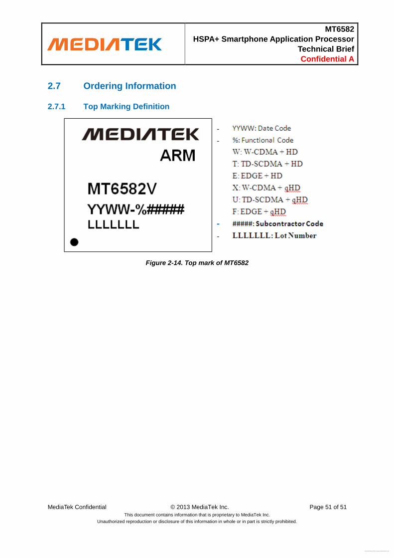
[email protected],time=2013-08-10 09:29:21,ip=112.90.37.152,doctitle=MT6582WG_Technical_Brief_v1.1.docx,company=Hexing_WCX
MT6582
HSPA+ Smartphone Application Processor
Technical Brief
Confidential A
MediaTek Confidential © 2013 MediaTek Inc. Page 51 of 51
This document contains information that is proprietary to MediaTek Inc.
Unauthorized reproduction or disclosure of this information in whole or in part is strictly prohibited.
2.7 Ordering Information
2.7.1 Top Marking Definition
Figure 2-14. Top mark of MT6582
Free Datasheet http://www.nDatasheet.com