
MSP432E4 SimpleLink™ Microcontrollers
28
1 SLAZ709 – October 2017 Submit Documentation Feedback Copyright © 2017, Texas Instruments Incorporated MSP432E4 SimpleLink™ Microcontrollers Silicon Errata SLAZ709 – October 2017 MSP432E4 SimpleLink™ Microcontrollers 1 Introduction This document describes known exceptions to the functional specifications for the SimpleLink™ MSP432E4 microcontrollers. Note that some features are not available on all devices in the series, so not all errata may apply to your device. See your device-specific data sheet for more details. For details on Arm ® Cortex ® -M4F CPU advisories, see the Arm ® Cortex ® -M4F Errata. 2 Device Nomenclature To designate the stages in the product development cycle, TI assigns prefixes to the part numbers of all MSP432™ MCU devices and support tools. Each MSP432 MCU commercial family member has one of two prefixes: MSP or XMS (for example, MSP432E411Y). Each support tools has one of two prefixes: MSP and MSPX. These prefixes represent evolutionary stages of product development from engineering prototypes (with XMS for devices and MSPX for tools) through fully qualified production devices and tools (with MSP for both devices and tools). Device development evolutionary flow: XMS – Experimental device that is not necessarily representative of the electrical specifications of the final device MSP – Fully qualified production device Support tool development evolutionary flow: MSPX – Development-support product that has not yet completed TI internal qualification testing. MSP – Fully-qualified development-support product XMS devices and MSPX development-support tools are shipped against the following disclaimer: "Developmental product is intended for internal evaluation purposes." MSP devices and MSP development-support tools have been characterized fully, and the quality and reliability of the device have been demonstrated fully. TI's standard warranty applies. Predictions show that prototype devices (XMS) have a greater failure rate than the standard production devices. TI recommends that these devices not be used in any production system because their expected end-use failure rate still is undefined. Only qualified production devices are to be used.
Transcript of MSP432E4 SimpleLink™ Microcontrollers
1SLAZ709–October 2017Submit Documentation Feedback
Copyright © 2017, Texas Instruments Incorporated
MSP432E4 SimpleLink™ Microcontrollers
Silicon ErrataSLAZ709–October 2017
MSP432E4 SimpleLink™ Microcontrollers
1 IntroductionThis document describes known exceptions to the functional specifications for the SimpleLink™MSP432E4 microcontrollers. Note that some features are not available on all devices in the series, so notall errata may apply to your device. See your device-specific data sheet for more details.
For details on Arm® Cortex®-M4F CPU advisories, see the Arm® Cortex®-M4F Errata.
2 Device NomenclatureTo designate the stages in the product development cycle, TI assigns prefixes to the part numbers of allMSP432™ MCU devices and support tools. Each MSP432 MCU commercial family member has one oftwo prefixes: MSP or XMS (for example, MSP432E411Y). Each support tools has one of two prefixes:MSP and MSPX. These prefixes represent evolutionary stages of product development from engineeringprototypes (with XMS for devices and MSPX for tools) through fully qualified production devices and tools(with MSP for both devices and tools).
Device development evolutionary flow:
XMS – Experimental device that is not necessarily representative of the electrical specifications of the finaldevice
MSP – Fully qualified production device
Support tool development evolutionary flow:
MSPX – Development-support product that has not yet completed TI internal qualification testing.
MSP – Fully-qualified development-support product
XMS devices and MSPX development-support tools are shipped against the following disclaimer:
"Developmental product is intended for internal evaluation purposes."
MSP devices and MSP development-support tools have been characterized fully, and the quality andreliability of the device have been demonstrated fully. TI's standard warranty applies.
Predictions show that prototype devices (XMS) have a greater failure rate than the standard productiondevices. TI recommends that these devices not be used in any production system because their expectedend-use failure rate still is undefined. Only qualified production devices are to be used.
Device Markings www.ti.com
2 SLAZ709–October 2017Submit Documentation Feedback
Copyright © 2017, Texas Instruments Incorporated
MSP432E4 SimpleLink™ Microcontrollers
3 Device MarkingsThe following are examples of the microcontroller package symbolization.
MSP432E411Y, 212-pin ZAD (NFBGA) package+----------------+| \TI/ | \TI/ = TI Logo| MSP432(TM) | (TM) = Trademark Symbol| E411YT | # = Die Revision| xxxxxxxxxx | O = Pin 1| O REV # |+----------------+
MSP432E401Y, 128-pin PDT (TQFP) package+----------------+| \TI/ xxxxxxxxx | \TI/ = TI Logo| MSP432 | # = Die Revision| E401YT | O = Pin 1| REV # || O |+----------------+
www.ti.com Errata Overview
3SLAZ709–October 2017Submit Documentation Feedback
Copyright © 2017, Texas Instruments Incorporated
MSP432E4 SimpleLink™ Microcontrollers
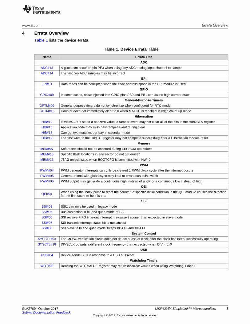
4 Errata OverviewTable 1 lists the device errata.
Table 1. Device Errata Table
Name Errata TitleADC
ADC#13 A glitch can occur on pin PE3 when using any ADC analog input channel to sampleADC#14 The first two ADC samples may be incorrect
EPIEPI#01 Data reads can be corrupted when the code address space in the EPI module is used
GPIOGPIO#09 In some cases, noise injected into GPIO pins PB0 and PB1 can cause high current draw
General-Purpose TimersGPTM#09 General-purpose timers do not synchronize when configured for RTC modeGPTM#15 Counter does not immediately clear to 0 when MATCH is reached in edge count up mode
HibernationHIB#10 If MEMCLR is set to a nonzero value, a tamper event may not clear all of the bits in the HIBDATA registerHIB#16 Application code may miss new tamper event during clearHIB#18 Can get two matches per day in calendar modeHIB#19 The first write to the HIBCTL register may not complete successfully after a Hibernation module reset
MemoryMEM#07 Soft resets should not be asserted during EEPROM operationsMEM#15 Specific flash locations in any sector do not get erasedMEM#16 JTAG unlock issue when BOOTCFG is committed with NW=0
PWMPWM#04 PWM generator interrupts can only be cleared 1 PWM clock cycle after the interrupt occursPWM#05 Generator load with global sync may lead to erroneous pulse widthPWM#06 PWM output may generate a continuous high instead of a low or a continuous low instead of high
QEI
QEI#01 When using the index pulse to reset the counter, a specific initial condition in the QEI module causes the directionfor the first count to be misread
SSISSI#03 SSI1 can only be used in legacy modeSSI#05 Bus contention in bi- and quad-mode of SSISSI#06 SSI receive FIFO time-out interrupt may assert sooner than expected in slave modeSSI#07 SSI transmit interrupt status bit is not latchedSSI#08 SSI slave in bi and quad mode swaps XDAT0 and XDAT1
System ControlSYSCTL#03 The MOSC verification circuit does not detect a loss of clock after the clock has been successfully operatingSYSCTL#18 DIVSCLK outputs a different clock frequency than expected when DIV = 0x0
USBUSB#04 Device sends SE0 in response to a USB bus reset
Watchdog TimersWDT#08 Reading the WDTVALUE register may return incorrect values when using Watchdog Timer 1
Errata Descriptions www.ti.com
4 SLAZ709–October 2017Submit Documentation Feedback
Copyright © 2017, Texas Instruments Incorporated
MSP432E4 SimpleLink™ Microcontrollers
5 Errata Descriptions
ADC#13 A glitch can occur on pin PE3 when using any ADC analog input channel tosample
Description A glitch may occur on PE3 when using any ADC analog input channel (AINx) to sample.This glitch can occur when PE3 is configured as an input channel and happens at theend of the ADC conversion. These glitches do not affect analog measurements on PE3when configured as AIN0 as long as the specified source resistance is met.
Workaround A 1-kΩ external pullup or pulldown on PE3 helps to minimize the magnitude of the glitchto 200 mV or less.
ADC#14 The First two ADC Samples may be Incorrect
Description The first two ADC samples taken after the ADC clock is enabled in the xCGCADCregister may be incorrect.
Workaround1. Reset the ADC peripheral using the SRADC register after the ADC peripheral clock is
enabled and before initializing the ADC and enabling the sample sequencer.2. If reconfiguration cannot be done by the application, then discard the first two
samples before processing the data.
EPI#01 Data reads can be corrupted when the code address space in the EPI module isused
Description The external code address space at address 0x1000.0000 is specified for the EPImodule using the ECSZ and ECADR fields in the EPI Address Map (EPIADDRMAP).However, data reads can be corrupted when using this address space.
Workaround Code cannot be executed from the 0x1000.0000 address space. The EPI addressspaces at 0x6000.0000 and 0x8000.0000 can be used instead.
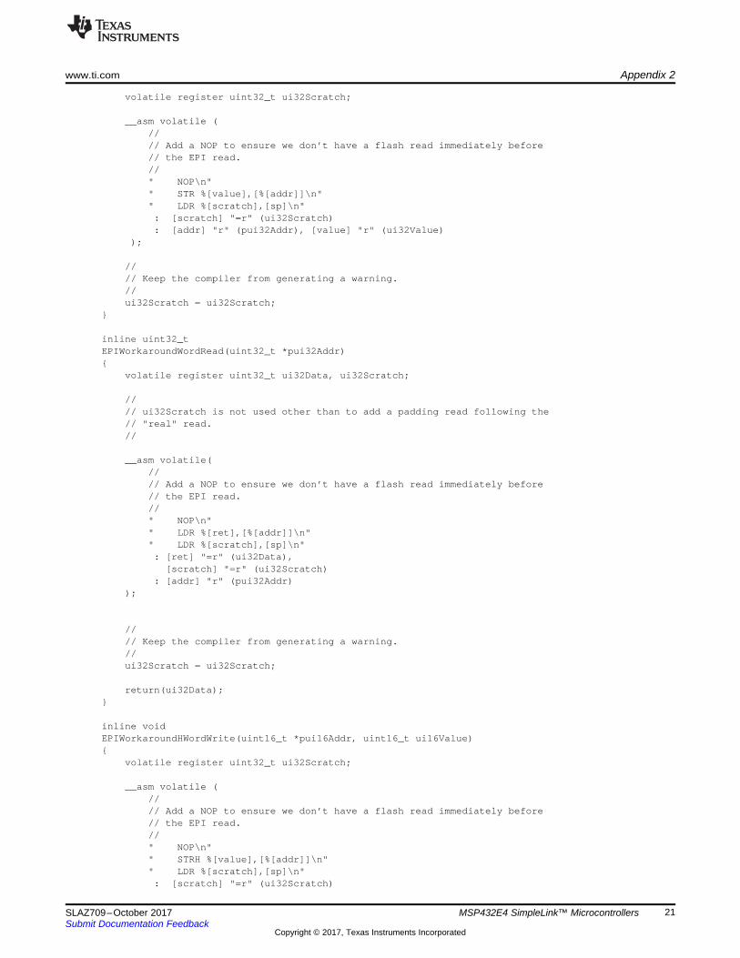
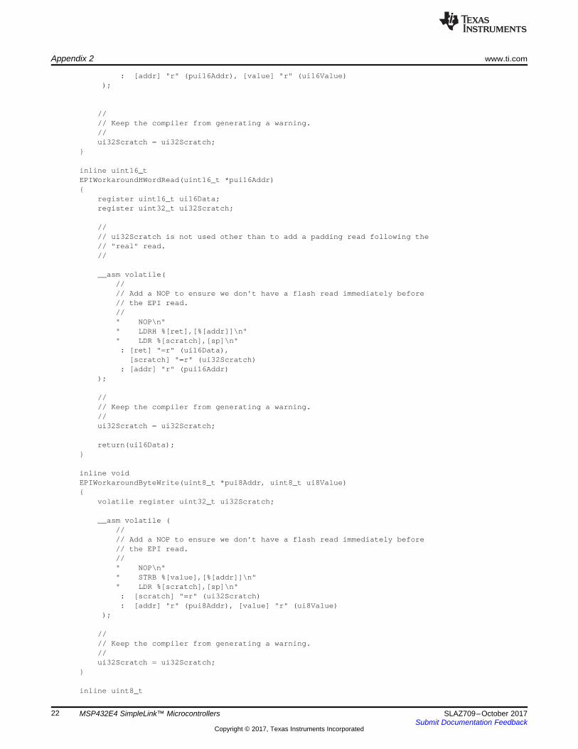
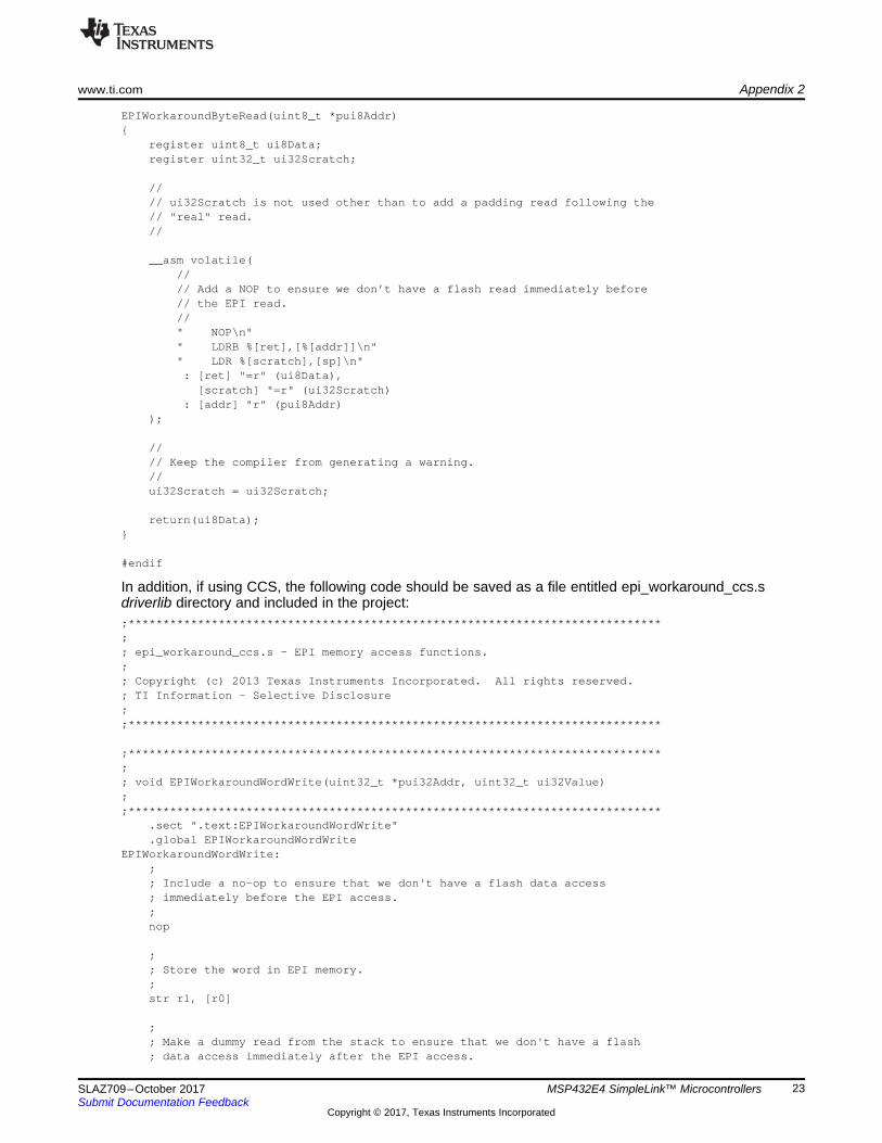
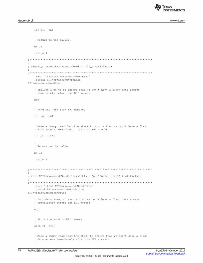
In addition, when reading from EPI memory mapped to the code address space at0x1000.0000, replace direct EPI memory reads through pointers with calls to theEPIWorkaroundWordRead(), EPIWorkaroundHWordRead() orEPIWorkaroundByteRead() functions depending on the data size for the read operation.Similarly, when writing to the EPI code address space, replace direct writes with calls tothe EPIWorkaroundWordWrite(), EPIWorkaroundHWordWrite() orEPIWorkaroundByteWrite() functions. These APIs are new and can be found inAppendix 2. For Keil, IAR, GCC, and Code Bench, these functions are defined as inlinefunctions in the epi.h file in the driverlib folder. For CCS, which doesn’t support thisstructure, these should be added to a new file placed in the \driverlib directory calledepi_workaround_ccs.s, and this file should be added to the project. Note that the newDriverLib APIs and the CCS file mentioned in Appendix 2 are included in the SimpleLinkMSP432 SDK.
www.ti.com Errata Descriptions
5SLAZ709–October 2017Submit Documentation Feedback
Copyright © 2017, Texas Instruments Incorporated
MSP432E4 SimpleLink™ Microcontrollers
GPIO#09 In some cases, noise injected into GPIO pins PB0 and PB1 can cause high currentdraw
Description A fast transition on either PB0 or PB1 can switch on a low resistance path between oneor both pins and ground potentially causing a high current draw.
This condition has been observed when the signal at the device pin has a rise time orfall time (measured from 10% to 90% of VDD) that is faster than 2 ns. The condition ismore likely to occur at high temperatures or in noisy environments. It can occur when thepin is in input or output mode or with any pin multiplexing options.
If the condition is induced while the pin is configured as an output GPIO, then changingthe pin state to low and then returning it to a high state at a lower temperature willresolve the condition.
Workaround1. Do not use PB0 and PB1. Connect both to GND through a 1-kΩ resistor and
configure them as GPIO inputs.2. If PB0 and PB1 are used as USB0ID and USB0VBUS, see the USB section of
System Design Guidelines for MSP432E4 Microcontrollers and confirm all guidelinescontained in the document are followed.
GPTM#09 General-purpose timers do not synchronize when configured for RTC mode
Description When attempting to synchronize the General-Purpose Timers using the GPTMSynchronize (GPTMSYNC) register, they do not synchronize if any of the timers areconfigured for RTC mode.
Workaround None.
GPTM#15 Counter does not immediately reset to 0 when MATCH is reached in edge count upmode
Description When configured for input edge count mode and count up mode, after counting to thematch value, the counter uses one additional edge to reset the timer to 0. As a result,after the first match event, all subsequent match events occur after the programmednumber of edge events plus one.
Workaround In software, account for one additional edge in the programmed edge count after the firstmatch interrupt is received.
HIB#10 If MEMCLR is set to a nonzero value, a tamper event may not clear all of the bits inthe HIBDATA register
Description If the MEMCLR bit field in the HIB Tamper Control (HIBTPCTL) register is set to a non-zero value, the Hibernation Data (HIBDATA) register may not clear the specified bits.The MEMCLR bit field provides the option to clear all, the upper half, lower half, or noneof the Hibernate memory on a tamper event.
Workaround After clearing the tamper event by setting the TPCLR bit, the application should clear thedata in the Hibernate memory in the HIBDATA register (write either the upper half, thelower half, or all of the bits to all zeros).
Errata Descriptions www.ti.com
6 SLAZ709–October 2017Submit Documentation Feedback
Copyright © 2017, Texas Instruments Incorporated
MSP432E4 SimpleLink™ Microcontrollers
HIB#16 Application code may miss new tamper event during clear
Description During the clear of a tamper event, a new tamper event could be missed or the tamperlog could be corrupted. The clear of a tamper event starts with the Tamper Clear(TPCLR) bit in the HIB Tamper Control register (HIBTPCTL) being written. The writetakes 3 rising edges of the 32.768-kHz clock to complete the clear.
Workaround To prevent missing a tamper event during these three Hibernate clock cycles andrestoring the tamper log to its reset state, workaround code must be implemented in theNMI handler as shown in Appendix 1. The new DriverLib APIs mentioned in Appendix 1are included in the SimpleLink MSP432E4 SDK.
HIB#18 Can get two matches per day in calendar mode
Description When the CAL24 bit in the Hibernation Calendar Control (HIBCALCTL) register is clear,the RTC counts in 12 hour, AM/PM mode. The AM/PM bit in the Hibernation CalendarMatch 0 (HIBCALM0) specifies whether the match should occur in the AM or the PM.However, this bit is ignored when determining if a match is occurring. As a result, anRTC match could occur twice in one day.
Workaround Adjust the match time to 24 hour mode before configuring the HIBCALM0 register andset the CAL24 bit. Alternatively, when the match occurs, check the AM/PM bit in theHibernation Calendar (HICAL0) register to determine if the match is correct.
HIB#19 The first write to the HIBCTL register may not complete successfully after aHibernation module reset
Description The initial write to the HIBCTL register may not occur if the Hibernation module is reset.The WRC bit in the HIBCTL register may not be set.
Workaround After a Hibernation module reset, check to see if the WRC bit is set and perform thefollowing:• If the WRC bit is not set within the maximum oscillator startup time, perform a
software reset of the Hibernation module and retry the HIBCTL write. The maximumoscillator startup time is given by the Hibernation XOSC startup time parameter,TSTART, in the Hibernation External Oscillator (XOSC) Input Characteristics table inthe Electrical Characteristics chapter of the data sheet.
• If the WRC bit is set but the HIBCTL write was not successful, retry the HIBCTLwrite.
www.ti.com Errata Descriptions
7SLAZ709–October 2017Submit Documentation Feedback
Copyright © 2017, Texas Instruments Incorporated
MSP432E4 SimpleLink™ Microcontrollers
MEM#07 Soft resets should not be asserted during EEPROM operations
Description EEPROM data may be corrupted if any of the following soft resets are asserted duringan EEPROM program or erase operation:• Software reset (SYSRESREQ)• Software peripheral reset of the EEPROM module• Watchdog reset (if configured as a system reset in the RESBEHAVCTL register)• MOSC failure reset• BOR reset (if configured as a system reset in the RESBEHAVCTL register)• External reset (if configured as a system reset in the RESBEHAVCTL register)• Writes to the HSSR register
Workaround Ensure that any of the above soft resets are not asserted during an EEPROM programor erase operation. The WORKING bit of the EEDONE register can be checked beforethe reset is asserted to see if an EEPROM program or erase operation is occurring. Softresets may occur when using a debugger and should be avoided during an EEPROMoperation. A reset such as the Watchdog reset can be mapped to an external reset usinga GPIO or Hibernate can be entered, if time is not a concern.
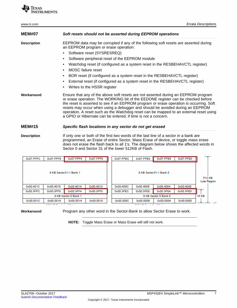
MEM#15 Specific flash locations in any sector do not get erased
Description If only one or both of the first two words of the last line of a sector in a bank areprogrammed, an Erase of entire Sector, Mass Erase of device, or toggle mass erasedoes not erase the flash back to all 1's. The diagram below shows the affected words inSector 0 and Sector 31 of the lower 512KB of Flash.
Workaround Program any other word in the Sector-Bank to allow Sector Erase to work.
NOTE: Toggle Mass Erase or Mass Erase will still not work.
Errata Descriptions www.ti.com
8 SLAZ709–October 2017Submit Documentation Feedback
Copyright © 2017, Texas Instruments Incorporated
MSP432E4 SimpleLink™ Microcontrollers
MEM#16 JTAG unlock issue when BOOTCFG is committed with NW=0
Description After configuring the BOOTCFG register with NW=0, DBG1=0 and DBG=1, the JTAGDebugger access is locked and cannot be unlocked by one Unlock Sequence Run.
Workaround The Unlock Sequence has to be run twice for the device to be unlocked.
PWM#04 PWM generator interrupts can only be cleared 1 PWM clock cycle after theinterrupt occurs
Description A write of 1 to the PWMxISC register is expected to clear the corresponding generatorinterrupt status on the next system clock. However, the write will clear the generatorinterrupt status on the next PWM clock. Any write to the PWMxISC to clear the interruptbefore the next PWM clock will be ignored and the interrupt will be re-asserted.
Workaround After the interrupt is asserted, the CPU must wait for one PWM clock cycle before writing1 to the PWMxISC to clear the corresponding generator interrupt status. The larger thePWM clock divider value, the longer the system delay to clear the interrupt.
PWM#05 Generator load with global sync may lead to erroneous pulse width
Description There is a condition where the generator timer may still count with the old value, but thenew comparator value gets loaded causing an erroneous high pulse width.
Workaround The application must use the interrupt status to write the value of the new load andcomparator values. When using the down count mode, clear the raw interrupt status bitfor the respective comparator down count match interrupt status bit, wait for it to be setagain and then update the new value for the load and comparator match.
PWM#06 PWM output may generate a continuous high instead of a low or a continuous lowinstead of high
Description When using PWM in UP-DOWN count mode, the PWM generator may generate acontinuous High instead of Low or continuous Low instead of High under the followingcondition:• The PWM generator is used with action for comparator A or B UP and DOWN to
control the PWM cycle.• The PWM comparator A or B is changed from a count of 2 or more to PWM Load
Count value.• A continuous High is generated if the invert option is enabled.• A continuous Low is generated if the invert option is disabled.
Workaround• Use DOWN count mode of PWM• When changing from any value (other than 1) to the PWM load count value in the
Comparator Load Register, always go to value of 1 before going to the PWM loadcount value.
www.ti.com Errata Descriptions
9SLAZ709–October 2017Submit Documentation Feedback
Copyright © 2017, Texas Instruments Incorporated
MSP432E4 SimpleLink™ Microcontrollers
QEI#01 When using the index pulse to reset the counter, a specific initial condition in theQEI module causes the direction for the first count to be misread
Description When using the index pulse to reset the counter with the following configuration in theQEI Control (QEICTL) register:• SIGMODE is 0 indicating quadrature mode• CAPMODE is 1 indicating both PhA and PhB edges are counted
and the following initial conditions:• Both PhA and PhB are 0• The next quadrature state is in the counterclockwise direction
the QEI interprets the state change as an update in the clockwise direction, which resultsin a position mismatch of 2.
Workaround None.
SSI#03 SSI1 can only be used in legacy mode
Description Bi-, quad-, and advance-modes of operation do not function correctly on the specifiedSSI module(s). As a result, any affected module can only be used for legacy operation.
Workaround Use SSI0, SSI2, or SSI3 for bi-, quad-, and advance-mode operation. Use SSI1 forlegacy-mode operation.
SSI#05 Bus contention in bi- and quad-mode of SSI
Description When the SSI is configured in Bi- or Quad-mode, and a read from external memory isperformed after the SSI is configured for Receive Mode, bus contention can occur on theSSI data pins on that first data read.
Workaround Perform a dummy read from memory before the first valid read operation afterconfiguring the SSI for Receive Mode (setting the DIR bit in the QSSI Control (SSICR1)register). For example:
SSIConfigSetExpClk(SSI0_BASE,SysCtlClockFreqSet (),SSI_FRF_MOTO_MODE_0, SSI_MODE_MASTER, 1000000, 8);SSIAdvModeSet(SSI0_BASE, SSI_ADV_BI_READ); //Receive Mode setSSIDataPut(SSI0_BASE, &pui32DataRx[ui32Index]); //intentional dummy writeSSIDataGetNonBlocking(SSI-_BASE, ui32Dummy); //dummy readSSIDataPut(SSI0_BASE, &pui32DataRx[ui32Index]); //intentional dummy writeSSIDataGetNonBlocking(SSI0_BASE, &pui32DataRx[0])); //first intentional readSSIDataPut(SSI0_BASE, &pui32DataRx[ui32Index]); //intentional dummy writeSSIDataGetNonBlocking(SSI0_BASE, &pui32DataRx[1])); //second intentional read
If the transfer normally requires any dummy operations, such as the intentional dummywrites shown above, the dummy read should occur before the normal dummyoperations.
Note that if your application is sensitive to the SSIClk, the dummy read outputs a clockcycle. Reconfigure the SSIClk pin to a GPIO input while performing the dummy read toprevent this from affecting your clock-sensitive application.
Errata Descriptions www.ti.com
10 SLAZ709–October 2017Submit Documentation Feedback
Copyright © 2017, Texas Instruments Incorporated
MSP432E4 SimpleLink™ Microcontrollers
SSI#06 SSI receive FIFO time-out interrupt may assert sooner than expected in slavemode
Description The SSI receive FIFO time-out interrupt may assert sooner than 32 system clock periodsin slave mode if the CPSDVSR field in the SSI Clock Prescale (SSICPSR) register is setto a value greater than 0x2. Master mode is not affected by this behavior.
Workaround In some cases, software can use the SCR field in the SSI Control 0 (SSICR0) register incombination with a CPSDVSR field value of 0x2 to attain the same SSI clock frequency.For example, if the desired serial clock rate is SysClk/48, then CPSDVSR = 0x2 andSCR = 0x17 can be used instead of CPSDVSR = 0x18 and SCR = 0x1 to achieve thesame clock rate, using the equation SSInCLK = SysClk / (CPSDVSR * (1 + SCR)). Ifthere is not a value of SCR that can be used with CPSDVSR = 0x2 to attain the requiredserial clock rate, then the receive FIFO time-out feature cannot be used.
SSI#07 SSI transmit interrupt status bit is not latched
Description SSI Transmit Interrupt Status Bit does not work correctly.• For Master Mode with interrupts when transmit FIFO is half full or less. SSIMIS will
be asserted every time the TXFIFO drops below half FIFO threshold causing theinterrupt to be asserted all the time even if SSIICR register is used to clear theInterrupt condition
Workaround In the interrupt handler on completion of the transfer from the buffer to SSIDR clear theSSIIM.TXIM to stop any further interrupts. When the next set of interrupts are requiredfor transmission then set the SSIIM.TXIM bit.
SSI#08 SSI slave in bi and quad mode swaps XDAT0 and XDAT1
Description The SSI Slave when in Bi or Quad Mode sends the data on XDAT0 to XDAT1 line andXDAT1 to XDAT0 line.
Workaround When transmitting the data from SSI Slave in Bi and Quad Mode the CPU must swapthe bits when writing to the Data Register SSIDR for the correct bit to be transmitted.When using uDMA CPU must write the swapped bits in the uDMA’s source buffer.
SYSCTL#03 The MOSC verification circuit does not detect a loss of clock after the clock hasbeen successfully operating
Description If the MOSC clock source has been powered up and operating correctly and issubsequently removed or flatlines, the MOSC verification circuit does not indicate anerror condition.
Workaround Use Watchdog module 1, which runs off of PIOSC, to reset the system if the MOSC fails.
www.ti.com Errata Descriptions
11SLAZ709–October 2017Submit Documentation Feedback
Copyright © 2017, Texas Instruments Incorporated
MSP432E4 SimpleLink™ Microcontrollers
SYSCTL#18 DIVSCLK Outputs a Different Clock Frequency than Expected when DIV = 0x0
Description In the Divisor and Source Clock Configuration (DIVSCLK) register, if the DIV bit field is0x0 (divided by 1), the clock output to the GPIO is not what is expected:• If the DIV bit field has not yet been adjusted in code, the clock frequency will be the
clock source defined in the SRC bit field divided by 32. For example, if SRC = 0x1(PIOSC) and DIV = 0x0, the clock output to the GPIO will have a frequency of 500kHz, derived from the PIOSC.
• If the DIV bit field has already been adjusted in code, the clock frequency will be theclock source defined in the SRC bit field divided by the previous DIV bit field value.For example, if SRC = 0x1 (PIOSC) and DIV was previously 0x1 (divided by 2) thenwritten to 0x0, the clock output to the GPIO will have a frequency of 8 MHz, derivedfrom the PIOSC.
Workaround If clock accuracy of the source is not a factor, certain frequencies can be achieved usinga non-zero DIV value and a different SRC value. For example, to achieve a 16 MHzclock, instead of SRC = 0x1 (PIOSC) and DIV = 0x0, use SRC = 0x0 (System Clock)and the respective DIV value (DIV = 0x4 (divided by 5) for a system clock of 80 MHz).
USB#04 Device sends SE0 in response to a USB bus reset
Description The USB Device sends an Single Ended Zero (SE0) bus state (USB0DP and USB0DMdriven low) in response to a USB bus reset from the Host. Per USB specification, theDevice should not drive these pins in the event of a USB bus reset. This does not affectUSB certification.
Workaround None.
WDT#08 Reading the WDTVALUE register may return incorrect values when usingWatchdog Timer 1
Description Incorrect values may be read from the Watchdog Value (WDTVALUE) register at theWatchdog Timer 1 base address when using Watchdog Timer 1.
Workaround None.
Appendix 1 www.ti.com
12 SLAZ709–October 2017Submit Documentation Feedback
Copyright © 2017, Texas Instruments Incorporated
MSP432E4 SimpleLink™ Microcontrollers
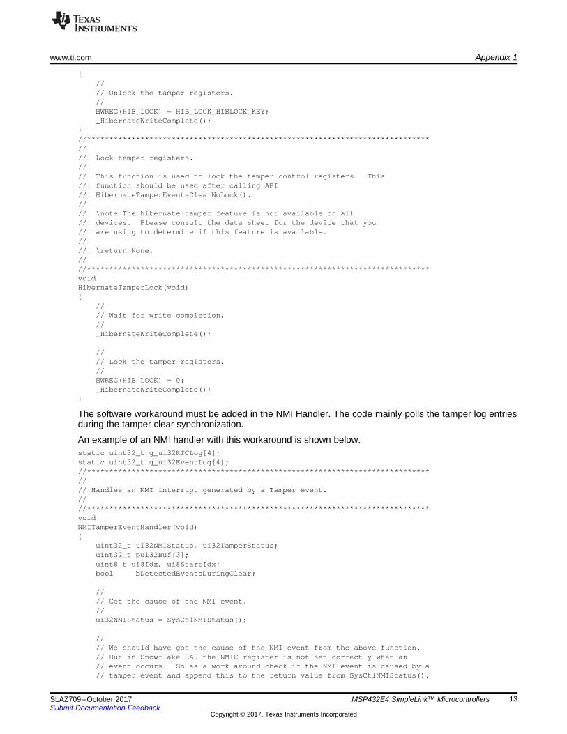
6 Appendix 1To address the erratum HIB#16, the HibernateTamperEventsClear() API must be replaced with thefollowing APIs:HibernateTamperEventsClearNoLock();HibernateTamperUnLock();HibernateTamperLock();
The API definitions are as follows://*****************************************************************************////! Clears the tamper feature events without Unlock and Lock.//!//! This function is used to clear all tamper events without unlock/locking//! the tamper control registers, so API HibernateTamperUnLock() should be//! called before this function, and API HibernateTamperLock() should be//! called after to ensure that tamper control registers are locked.//!//! This function doesn't block until the write is complete.//! Therefore, care must be taken to ensure the next immediate write will//! occure only after the write complete bit is set.//!//! This function is used to implement a software workaround in NMI interrupt//! handler to fix an issue when a new tamper event could be missed during//! the clear of current tamper event.//!//! \note The hibernate tamper feature is not available on all//! devices. Please consult the data sheet for the device that you//! are using to determine if this feature is available.//!//! \return None.////*****************************************************************************voidHibernateTamperEventsClearNoLock(void)
//// Wait for write completion.//_HibernateWriteComplete();
////// Set the tamper event clear bit.//HWREG(HIB_TPCTL) |= HIB_TPCTL_TPCLR;
//*****************************************************************************////! Unlock temper registers.//!//! This function is used to unlock the temper control registers. This//! function should be only used before calling API//! HibernateTamperEventsClearNoLock().//!//! \note The hibernate tamper feature is not available on all//! devices. Please consult the data sheet for the device that you//! are using to determine if this feature is available.//!//! \return None.////*****************************************************************************voidHibernateTamperUnLock(void)
www.ti.com Appendix 1
13SLAZ709–October 2017Submit Documentation Feedback
Copyright © 2017, Texas Instruments Incorporated
MSP432E4 SimpleLink™ Microcontrollers
//// Unlock the tamper registers.//HWREG(HIB_LOCK) = HIB_LOCK_HIBLOCK_KEY;_HibernateWriteComplete();
//*****************************************************************************////! Lock temper registers.//!//! This function is used to lock the temper control registers. This//! function should be used after calling API//! HibernateTamperEventsClearNoLock().//!//! \note The hibernate tamper feature is not available on all//! devices. Please consult the data sheet for the device that you//! are using to determine if this feature is available.//!//! \return None.////*****************************************************************************voidHibernateTamperLock(void)
//// Wait for write completion.//_HibernateWriteComplete();
//// Lock the tamper registers.//HWREG(HIB_LOCK) = 0;_HibernateWriteComplete();
The software workaround must be added in the NMI Handler. The code mainly polls the tamper log entriesduring the tamper clear synchronization.
An example of an NMI handler with this workaround is shown below.static uint32_t g_ui32RTCLog[4];static uint32_t g_ui32EventLog[4];//*****************************************************************************//// Handles an NMI interrupt generated by a Tamper event.////*****************************************************************************voidNMITamperEventHandler(void)
uint32_t ui32NMIStatus, ui32TamperStatus;uint32_t pui32Buf[3];uint8_t ui8Idx, ui8StartIdx;bool bDetectedEventsDuringClear;
//// Get the cause of the NMI event.//ui32NMIStatus = SysCtlNMIStatus();
//// We should have got the cause of the NMI event from the above function.// But in Snowflake RA0 the NMIC register is not set correctly when an// event occurs. So as a work around check if the NMI event is caused by a// tamper event and append this to the return value from SysCtlNMIStatus().
Appendix 1 www.ti.com
14 SLAZ709–October 2017Submit Documentation Feedback
Copyright © 2017, Texas Instruments Incorporated
MSP432E4 SimpleLink™ Microcontrollers
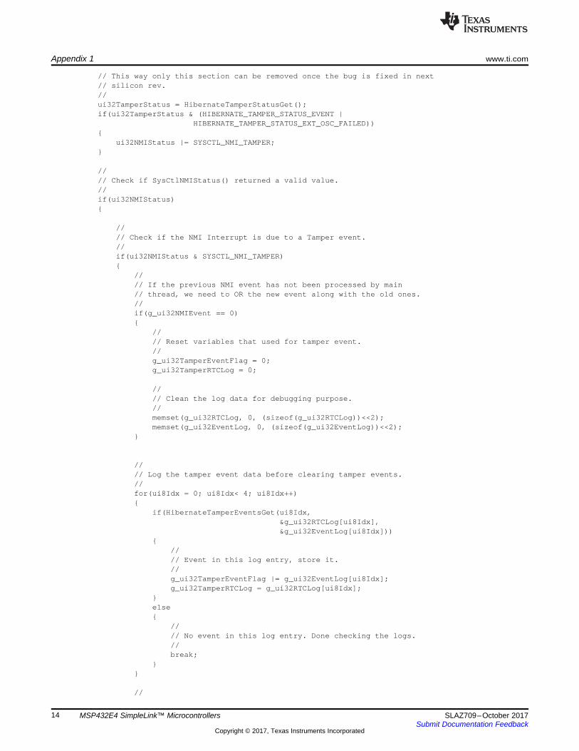
// This way only this section can be removed once the bug is fixed in next// silicon rev.//ui32TamperStatus = HibernateTamperStatusGet();if(ui32TamperStatus & (HIBERNATE_TAMPER_STATUS_EVENT |
HIBERNATE_TAMPER_STATUS_EXT_OSC_FAILED))
ui32NMIStatus |= SYSCTL_NMI_TAMPER;
//// Check if SysCtlNMIStatus() returned a valid value.//if(ui32NMIStatus)
//// Check if the NMI Interrupt is due to a Tamper event.//if(ui32NMIStatus & SYSCTL_NMI_TAMPER)
//// If the previous NMI event has not been processed by main// thread, we need to OR the new event along with the old ones.//if(g_ui32NMIEvent == 0)
//// Reset variables that used for tamper event.//g_ui32TamperEventFlag = 0;g_ui32TamperRTCLog = 0;
//// Clean the log data for debugging purpose.//memset(g_ui32RTCLog, 0, (sizeof(g_ui32RTCLog))<<2);memset(g_ui32EventLog, 0, (sizeof(g_ui32EventLog))<<2);
//// Log the tamper event data before clearing tamper events.//for(ui8Idx = 0; ui8Idx< 4; ui8Idx++)
if(HibernateTamperEventsGet(ui8Idx,&g_ui32RTCLog[ui8Idx],&g_ui32EventLog[ui8Idx]))
//// Event in this log entry, store it.//g_ui32TamperEventFlag |= g_ui32EventLog[ui8Idx];g_ui32TamperRTCLog = g_ui32RTCLog[ui8Idx];
else
//// No event in this log entry. Done checking the logs.//break;
//
www.ti.com Appendix 1
15SLAZ709–October 2017Submit Documentation Feedback
Copyright © 2017, Texas Instruments Incorporated
MSP432E4 SimpleLink™ Microcontrollers
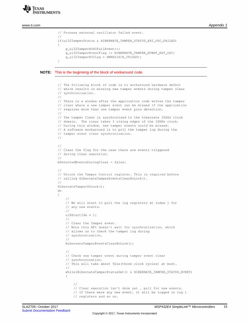
// Process external oscillator failed event.//if(ui32TamperStatus & HIBERNATE_TAMPER_STATUS_EXT_OSC_FAILED)
g_ui32TamperXOSCFailEvent++;g_ui32TamperEventFlag |= HIBERNATE_TAMPER_EVENT_EXT_OSC;g_ui32TamperRTCLog = HWREG(HIB_TPLOG0);
NOTE: This is the beginning of the block of workaround code.
// The following block of code is to workaround hardware defect// which results in missing new tamper events during tamper clear// synchronization.//// There is a window after the application code writes the tamper// clear where a new tamper event can be missed if the application// requires more than one tamper event pins detection.//// The tamper Clear is synchronized to the hibernate 32kHz clock// domain. The clear takes 3 rising edges of the 32KHz clock.// During this window, new tamper events could be missed.// A software workaround is to poll the tamper log during the// tamper event clear synchronization.//
//// Clear the flag for the case there are events triggered// during clear execution.//bDetectedEventsDuringClear = false;
//// Unlock the Tamper Control register. This is required before// calling HibernateTamperEventsClearNoLock().//HibernateTamperUnLock();do
//// We will start to poll the log registers at index 1 for// any new events.//ui8StartIdx = 1;//// Clear the Tamper event.// Note this API doesn't wait for synchronization, which// allows us to check the tamper log during// synchronization.//HibernateTamperEventsClearNoLock();
//// Check new tamper event during tamper event clear// synchronization.// This will take about 92us(three clock cycles) at most.//while(HibernateTamperStatusGet() & HIBERNATE_TAMPER_STATUS_EVENT)
//// Clear execution isn't done yet , poll for new events.// If there were any new event, it will be logged in log 1// registers and so on.
Appendix 1 www.ti.com
16 SLAZ709–October 2017Submit Documentation Feedback
Copyright © 2017, Texas Instruments Incorporated
MSP432E4 SimpleLink™ Microcontrollers
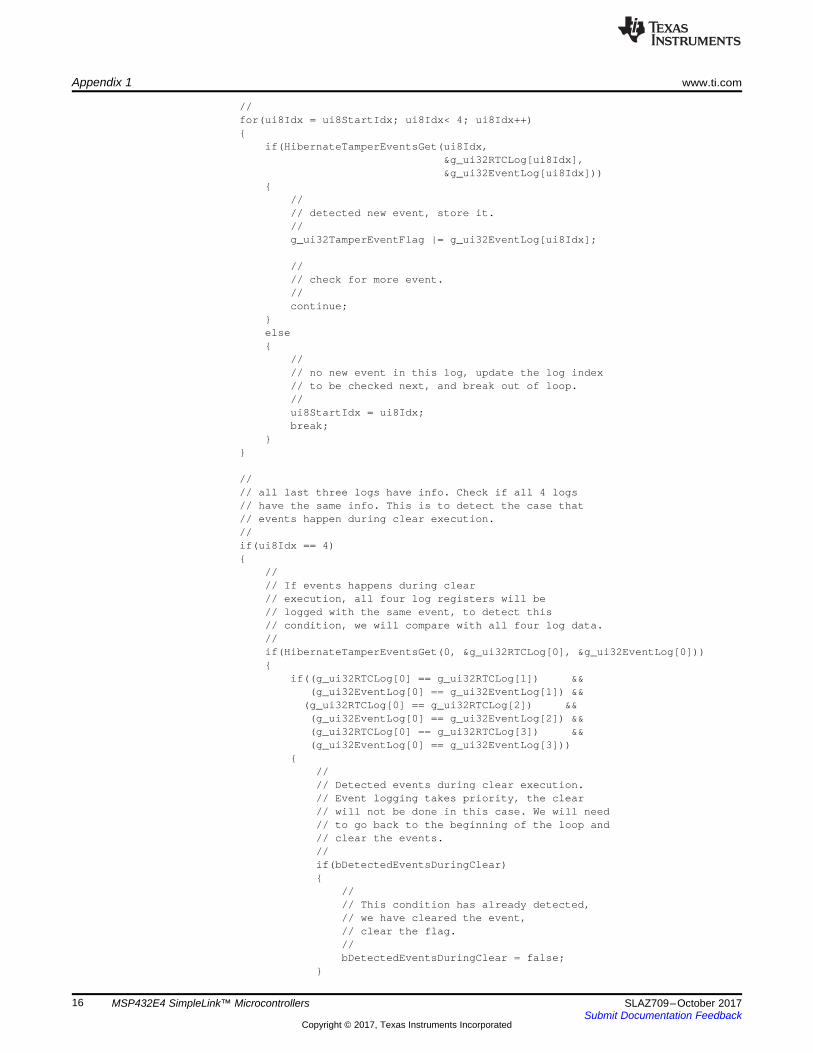
//for(ui8Idx = ui8StartIdx; ui8Idx< 4; ui8Idx++)
if(HibernateTamperEventsGet(ui8Idx,&g_ui32RTCLog[ui8Idx],&g_ui32EventLog[ui8Idx]))
//// detected new event, store it.//g_ui32TamperEventFlag |= g_ui32EventLog[ui8Idx];
//// check for more event.//continue;
else
//// no new event in this log, update the log index// to be checked next, and break out of loop.//ui8StartIdx = ui8Idx;break;
//// all last three logs have info. Check if all 4 logs// have the same info. This is to detect the case that// events happen during clear execution.//if(ui8Idx == 4)
//// If events happens during clear// execution, all four log registers will be// logged with the same event, to detect this// condition, we will compare with all four log data.//if(HibernateTamperEventsGet(0, &g_ui32RTCLog[0], &g_ui32EventLog[0]))
if((g_ui32RTCLog[0] == g_ui32RTCLog[1]) &&(g_ui32EventLog[0] == g_ui32EventLog[1]) &&
(g_ui32RTCLog[0] == g_ui32RTCLog[2]) &&(g_ui32EventLog[0] == g_ui32EventLog[2]) &&(g_ui32RTCLog[0] == g_ui32RTCLog[3]) &&(g_ui32EventLog[0] == g_ui32EventLog[3]))
//// Detected events during clear execution.// Event logging takes priority, the clear// will not be done in this case. We will need// to go back to the beginning of the loop and// clear the events.//if(bDetectedEventsDuringClear)
//// This condition has already detected,// we have cleared the event,// clear the flag.//bDetectedEventsDuringClear = false;
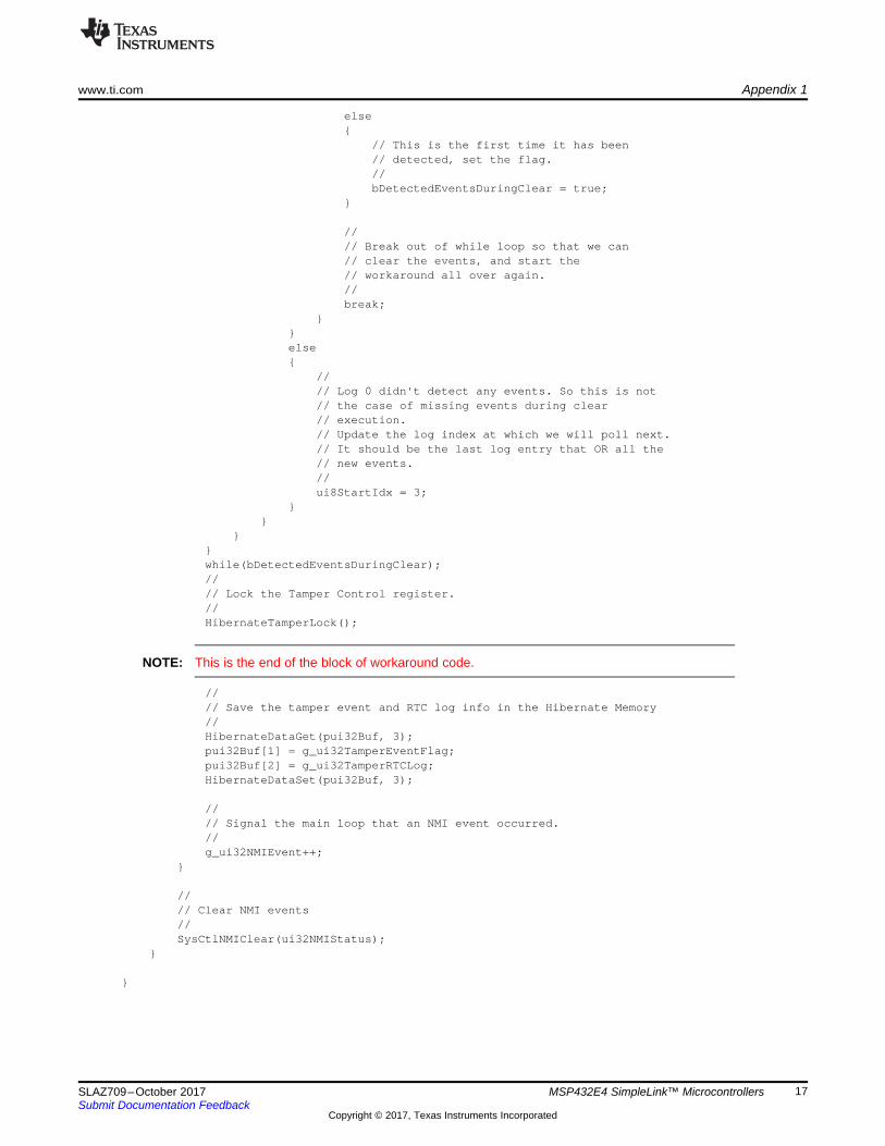
www.ti.com Appendix 1
17SLAZ709–October 2017Submit Documentation Feedback
Copyright © 2017, Texas Instruments Incorporated
MSP432E4 SimpleLink™ Microcontrollers
else
// This is the first time it has been// detected, set the flag.//bDetectedEventsDuringClear = true;
//// Break out of while loop so that we can// clear the events, and start the// workaround all over again.//break;
else
//// Log 0 didn't detect any events. So this is not// the case of missing events during clear// execution.// Update the log index at which we will poll next.// It should be the last log entry that OR all the// new events.//ui8StartIdx = 3;
while(bDetectedEventsDuringClear);//// Lock the Tamper Control register.//HibernateTamperLock();
NOTE: This is the end of the block of workaround code.
//// Save the tamper event and RTC log info in the Hibernate Memory//HibernateDataGet(pui32Buf, 3);pui32Buf[1] = g_ui32TamperEventFlag;pui32Buf[2] = g_ui32TamperRTCLog;HibernateDataSet(pui32Buf, 3);
//// Signal the main loop that an NMI event occurred.//g_ui32NMIEvent++;
//// Clear NMI events//SysCtlNMIClear(ui32NMIStatus);
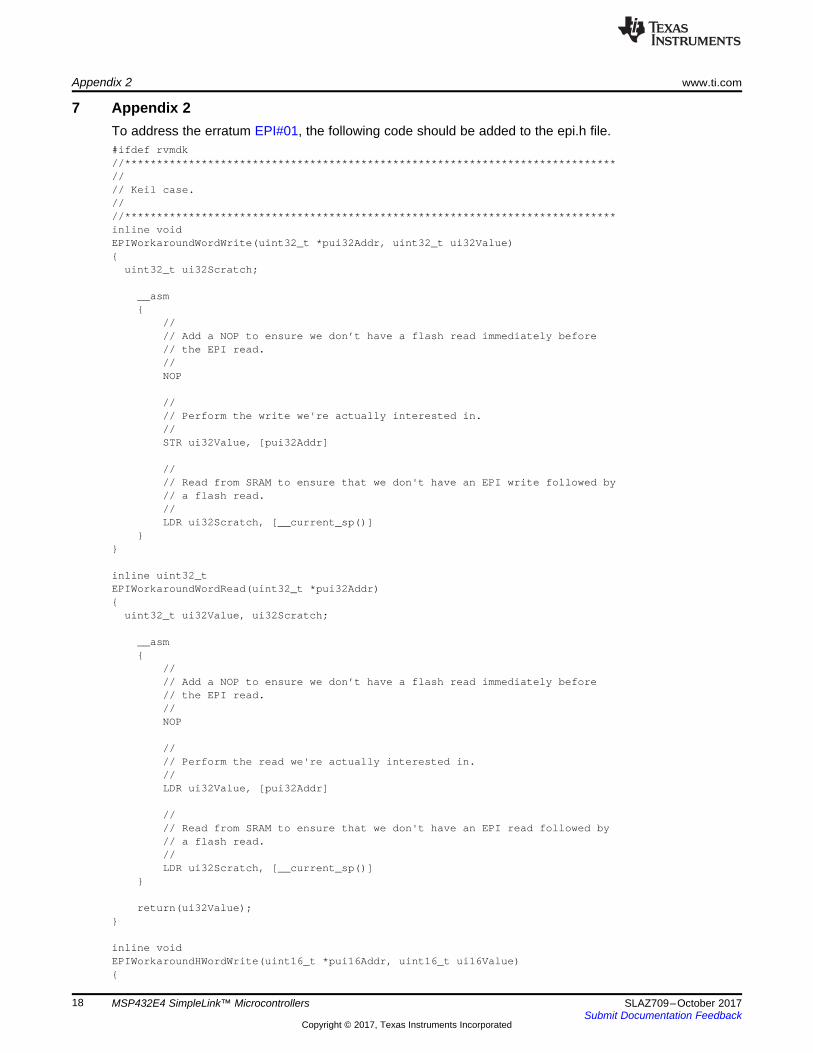
Appendix 2 www.ti.com
18 SLAZ709–October 2017Submit Documentation Feedback
Copyright © 2017, Texas Instruments Incorporated
MSP432E4 SimpleLink™ Microcontrollers
7 Appendix 2To address the erratum EPI#01, the following code should be added to the epi.h file.#ifdef rvmdk//*****************************************************************************//// Keil case.////*****************************************************************************inline voidEPIWorkaroundWordWrite(uint32_t *pui32Addr, uint32_t ui32Value)
uint32_t ui32Scratch;
__asm
//// Add a NOP to ensure we don’t have a flash read immediately before// the EPI read.//NOP
//// Perform the write we're actually interested in.//STR ui32Value, [pui32Addr]
//// Read from SRAM to ensure that we don't have an EPI write followed by// a flash read.//LDR ui32Scratch, [__current_sp()]
inline uint32_tEPIWorkaroundWordRead(uint32_t *pui32Addr)
uint32_t ui32Value, ui32Scratch;
__asm
//// Add a NOP to ensure we don’t have a flash read immediately before// the EPI read.//NOP
//// Perform the read we're actually interested in.//LDR ui32Value, [pui32Addr]
//// Read from SRAM to ensure that we don't have an EPI read followed by// a flash read.//LDR ui32Scratch, [__current_sp()]
return(ui32Value);
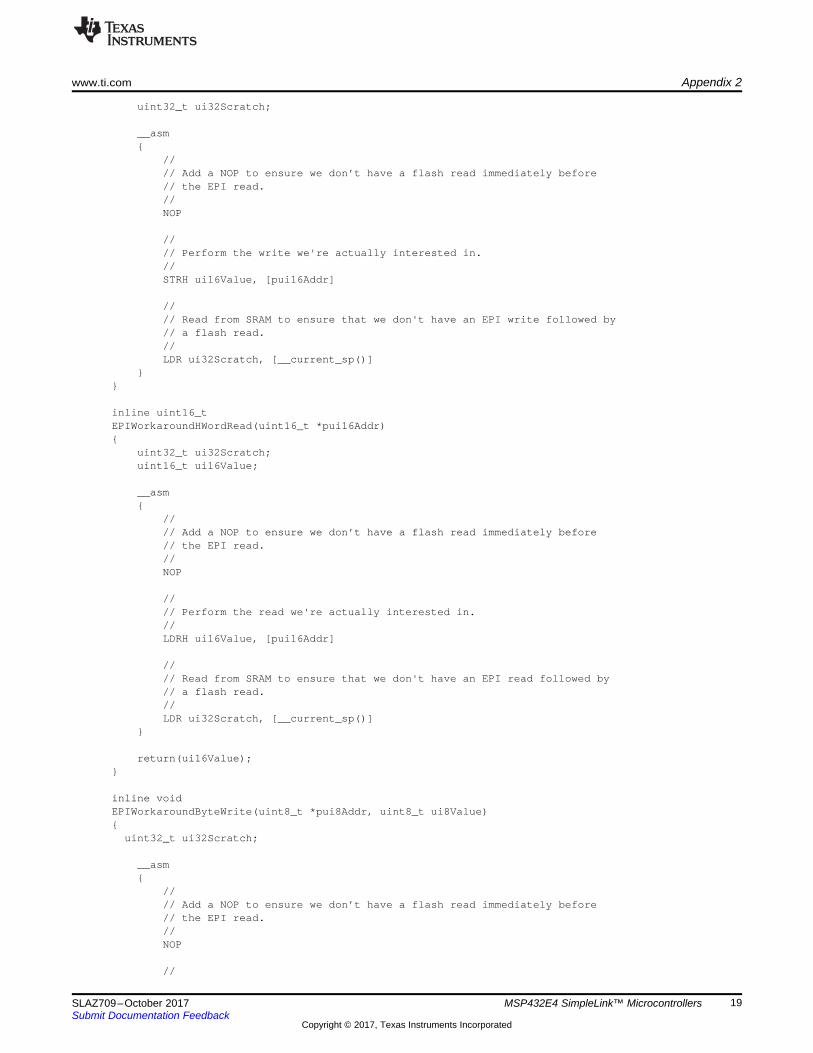
inline voidEPIWorkaroundHWordWrite(uint16_t *pui16Addr, uint16_t ui16Value)
www.ti.com Appendix 2
19SLAZ709–October 2017Submit Documentation Feedback
Copyright © 2017, Texas Instruments Incorporated
MSP432E4 SimpleLink™ Microcontrollers
uint32_t ui32Scratch;
__asm
//// Add a NOP to ensure we don’t have a flash read immediately before// the EPI read.//NOP
//// Perform the write we're actually interested in.//STRH ui16Value, [pui16Addr]
//// Read from SRAM to ensure that we don't have an EPI write followed by// a flash read.//LDR ui32Scratch, [__current_sp()]
inline uint16_tEPIWorkaroundHWordRead(uint16_t *pui16Addr)
uint32_t ui32Scratch;uint16_t ui16Value;
__asm
//// Add a NOP to ensure we don’t have a flash read immediately before// the EPI read.//NOP
//// Perform the read we're actually interested in.//LDRH ui16Value, [pui16Addr]
//// Read from SRAM to ensure that we don't have an EPI read followed by// a flash read.//LDR ui32Scratch, [__current_sp()]
return(ui16Value);
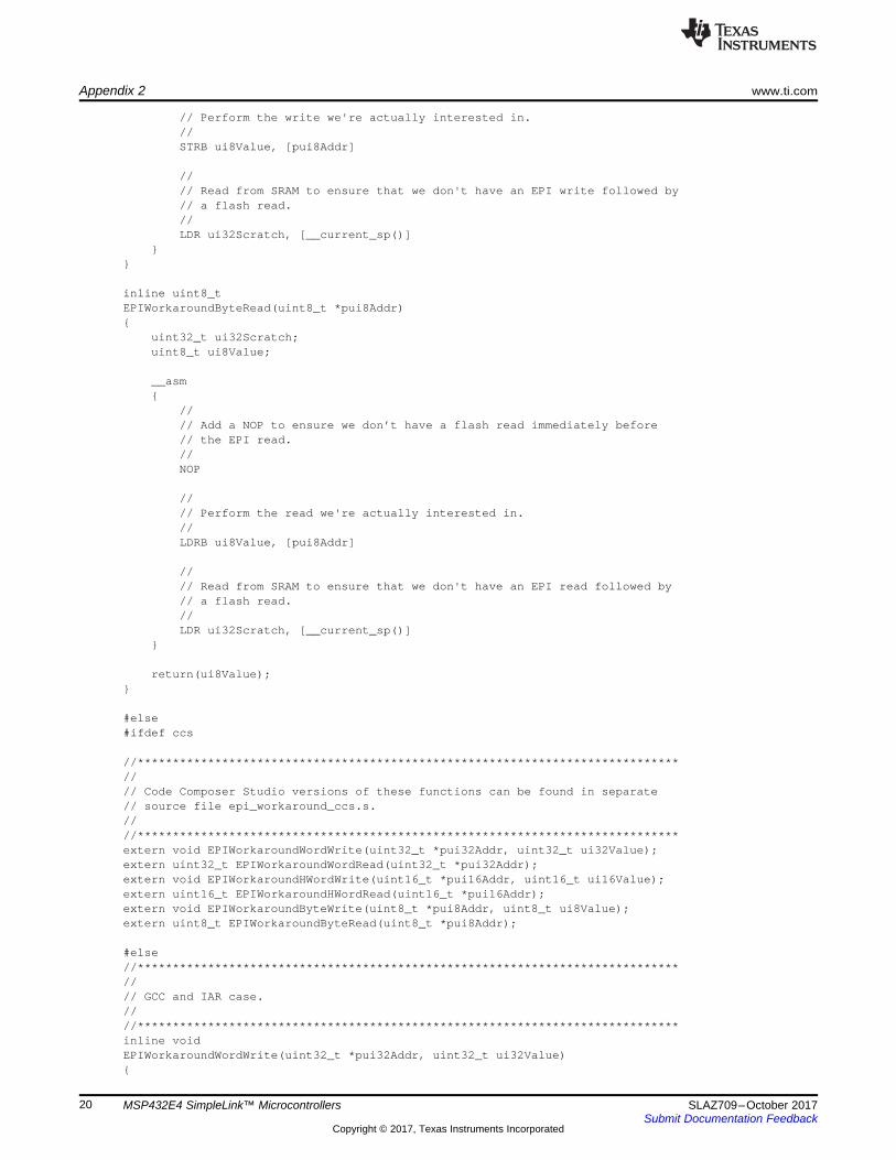
inline voidEPIWorkaroundByteWrite(uint8_t *pui8Addr, uint8_t ui8Value)
uint32_t ui32Scratch;
__asm
//// Add a NOP to ensure we don’t have a flash read immediately before// the EPI read.//NOP
//
Appendix 2 www.ti.com
20 SLAZ709–October 2017Submit Documentation Feedback
Copyright © 2017, Texas Instruments Incorporated
MSP432E4 SimpleLink™ Microcontrollers
// Perform the write we're actually interested in.//STRB ui8Value, [pui8Addr]
//// Read from SRAM to ensure that we don't have an EPI write followed by// a flash read.//LDR ui32Scratch, [__current_sp()]
inline uint8_tEPIWorkaroundByteRead(uint8_t *pui8Addr)
uint32_t ui32Scratch;uint8_t ui8Value;
__asm
//// Add a NOP to ensure we don’t have a flash read immediately before// the EPI read.//NOP
//// Perform the read we're actually interested in.//LDRB ui8Value, [pui8Addr]
//// Read from SRAM to ensure that we don't have an EPI read followed by// a flash read.//LDR ui32Scratch, [__current_sp()]
return(ui8Value);
#else#ifdef ccs
//*****************************************************************************//// Code Composer Studio versions of these functions can be found in separate// source file epi_workaround_ccs.s.////*****************************************************************************extern void EPIWorkaroundWordWrite(uint32_t *pui32Addr, uint32_t ui32Value);extern uint32_t EPIWorkaroundWordRead(uint32_t *pui32Addr);extern void EPIWorkaroundHWordWrite(uint16_t *pui16Addr, uint16_t ui16Value);extern uint16_t EPIWorkaroundHWordRead(uint16_t *pui16Addr);extern void EPIWorkaroundByteWrite(uint8_t *pui8Addr, uint8_t ui8Value);extern uint8_t EPIWorkaroundByteRead(uint8_t *pui8Addr);
#else//*****************************************************************************//// GCC and IAR case.////*****************************************************************************inline voidEPIWorkaroundWordWrite(uint32_t *pui32Addr, uint32_t ui32Value)
www.ti.com Appendix 2
21SLAZ709–October 2017Submit Documentation Feedback
Copyright © 2017, Texas Instruments Incorporated
MSP432E4 SimpleLink™ Microcontrollers
volatile register uint32_t ui32Scratch;
__asm volatile (//// Add a NOP to ensure we don’t have a flash read immediately before// the EPI read.//" NOP\n"" STR %[value],[%[addr]]\n"" LDR %[scratch],[sp]\n"
: [scratch] "=r" (ui32Scratch): [addr] "r" (pui32Addr), [value] "r" (ui32Value)
);
//// Keep the compiler from generating a warning.//ui32Scratch = ui32Scratch;
inline uint32_tEPIWorkaroundWordRead(uint32_t *pui32Addr)
volatile register uint32_t ui32Data, ui32Scratch;
//// ui32Scratch is not used other than to add a padding read following the// "real" read.//
__asm volatile(//// Add a NOP to ensure we don’t have a flash read immediately before// the EPI read.//" NOP\n"" LDR %[ret],[%[addr]]\n"" LDR %[scratch],[sp]\n"
: [ret] "=r" (ui32Data),[scratch] "=r" (ui32Scratch)
: [addr] "r" (pui32Addr));
//// Keep the compiler from generating a warning.//ui32Scratch = ui32Scratch;
return(ui32Data);
inline voidEPIWorkaroundHWordWrite(uint16_t *pui16Addr, uint16_t ui16Value)
volatile register uint32_t ui32Scratch;
__asm volatile (//// Add a NOP to ensure we don’t have a flash read immediately before// the EPI read.//" NOP\n"" STRH %[value],[%[addr]]\n"" LDR %[scratch],[sp]\n"
: [scratch] "=r" (ui32Scratch)
Appendix 2 www.ti.com
22 SLAZ709–October 2017Submit Documentation Feedback
Copyright © 2017, Texas Instruments Incorporated
MSP432E4 SimpleLink™ Microcontrollers
: [addr] "r" (pui16Addr), [value] "r" (ui16Value));
//// Keep the compiler from generating a warning.//ui32Scratch = ui32Scratch;
inline uint16_tEPIWorkaroundHWordRead(uint16_t *pui16Addr)
register uint16_t ui16Data;register uint32_t ui32Scratch;
//// ui32Scratch is not used other than to add a padding read following the// "real" read.//
__asm volatile(//// Add a NOP to ensure we don’t have a flash read immediately before// the EPI read.//" NOP\n"" LDRH %[ret],[%[addr]]\n"" LDR %[scratch],[sp]\n"
: [ret] "=r" (ui16Data),[scratch] "=r" (ui32Scratch)
: [addr] "r" (pui16Addr));
//// Keep the compiler from generating a warning.//ui32Scratch = ui32Scratch;
return(ui16Data);
inline voidEPIWorkaroundByteWrite(uint8_t *pui8Addr, uint8_t ui8Value)
volatile register uint32_t ui32Scratch;
__asm volatile (//// Add a NOP to ensure we don’t have a flash read immediately before// the EPI read.//" NOP\n"" STRB %[value],[%[addr]]\n"" LDR %[scratch],[sp]\n"
: [scratch] "=r" (ui32Scratch): [addr] "r" (pui8Addr), [value] "r" (ui8Value)
);
//// Keep the compiler from generating a warning.//ui32Scratch = ui32Scratch;
inline uint8_t
www.ti.com Appendix 2
23SLAZ709–October 2017Submit Documentation Feedback
Copyright © 2017, Texas Instruments Incorporated
MSP432E4 SimpleLink™ Microcontrollers
EPIWorkaroundByteRead(uint8_t *pui8Addr)
register uint8_t ui8Data;register uint32_t ui32Scratch;
//// ui32Scratch is not used other than to add a padding read following the// "real" read.//
__asm volatile(//// Add a NOP to ensure we don’t have a flash read immediately before// the EPI read.//" NOP\n"" LDRB %[ret],[%[addr]]\n"" LDR %[scratch],[sp]\n"
: [ret] "=r" (ui8Data),[scratch] "=r" (ui32Scratch)
: [addr] "r" (pui8Addr));
//// Keep the compiler from generating a warning.//ui32Scratch = ui32Scratch;
return(ui8Data);
#endif
In addition, if using CCS, the following code should be saved as a file entitled epi_workaround_ccs.sdriverlib directory and included in the project:;*****************************************************************************;; epi_workaround_ccs.s - EPI memory access functions.;; Copyright (c) 2013 Texas Instruments Incorporated. All rights reserved.; TI Information - Selective Disclosure;;*****************************************************************************
;*****************************************************************************;; void EPIWorkaroundWordWrite(uint32_t *pui32Addr, uint32_t ui32Value);;*****************************************************************************
.sect ".text:EPIWorkaroundWordWrite"
.global EPIWorkaroundWordWriteEPIWorkaroundWordWrite:
;; Include a no-op to ensure that we don't have a flash data access; immediately before the EPI access.;nop
;; Store the word in EPI memory.;str r1, [r0]
;; Make a dummy read from the stack to ensure that we don't have a flash; data access immediately after the EPI access.
Appendix 2 www.ti.com
24 SLAZ709–October 2017Submit Documentation Feedback
Copyright © 2017, Texas Instruments Incorporated
MSP432E4 SimpleLink™ Microcontrollers
;ldr r1, [sp]
;; Return to the caller.;bx lr
.align 4
;*****************************************************************************;; uint32_t EPIWorkaroundWordRead(uint32_t *pui32Addr);;*****************************************************************************
.sect ".text:EPIWorkaroundWordRead"
.global EPIWorkaroundWordReadEPIWorkaroundWordRead:
;; Include a no-op to ensure that we don't have a flash data access; immediately before the EPI access.;nop
;; Read the word from EPI memory.;ldr r0, [r0]
;; Make a dummy read from the stack to ensure that we don't have a flash; data access immediately after the EPI access.;ldr r1, [r13]
;; Return to the caller.;bx lr
.align 4
;*****************************************************************************;; void EPIWorkaroundHWordWrite(uint16_t *pui16Addr, uint16_t ui16Value);;*****************************************************************************
.sect ".text:EPIWorkaroundHWordWrite"
.global EPIWorkaroundHWordWriteEPIWorkaroundHWordWrite:
;; Include a no-op to ensure that we don't have a flash data access; immediately before the EPI access.;nop
;; Store the word in EPI memory.;strh r1, [r0]
;; Make a dummy read from the stack to ensure that we don't have a flash; data access immediately after the EPI access.;
www.ti.com Appendix 2
25SLAZ709–October 2017Submit Documentation Feedback
Copyright © 2017, Texas Instruments Incorporated
MSP432E4 SimpleLink™ Microcontrollers
ldr r1, [sp]
;; Return to the caller.;bx lr
.align 4
;*****************************************************************************;; uint16_t EPIWorkaroundHWordRead(uint16_t *pui16Addr);;*****************************************************************************
.sect ".text:EPIWorkaroundHWordRead"
.global EPIWorkaroundHWordReadEPIWorkaroundHWordRead:
;; Include a no-op to ensure that we don't have a flash data access; immediately before the EPI access.;nop
;; Read the half word from EPI memory.;ldrh r0, [r0]
;; Make a dummy read from the stack to ensure that we don't have a flash; data access immediately after the EPI access.;ldr r1, [r13]
;; Return to the caller.;bx lr
.align 4
;*****************************************************************************;; void EPIWorkaroundByteWrite(uint8_t *pui8Addr, uint8_t ui8Value);;*****************************************************************************
.sect ".text:EPIWorkaroundByteWrite"
.global EPIWorkaroundByteWriteEPIWorkaroundByteWrite:
;; Include a no-op to ensure that we don't have a flash data access; immediately before the EPI access.;nop
;; Store the byte in EPI memory.;strb r1, [r0]
;; Make a dummy read from the stack to ensure that we don't have a flash; data access immediately after the EPI access.;ldr r1, [sp]
Appendix 2 www.ti.com
26 SLAZ709–October 2017Submit Documentation Feedback
Copyright © 2017, Texas Instruments Incorporated
MSP432E4 SimpleLink™ Microcontrollers
;; Return to the caller.;bx lr
.align 4
;*****************************************************************************;; uint8_t EPIWorkaroundByteRead(uint8_t *pui8Addr);;*****************************************************************************
.sect ".text:EPIWorkaroundByteRead"
.global EPIWorkaroundByteReadEPIWorkaroundByteRead:
;; Include a no-op to ensure that we don't have a flash data access; immediately before the EPI access.;nop
;; Read the byte from EPI memory.;ldrb r0, [r0]
;; Make a dummy read from the stack to ensure that we don't have a flash; data access immediately after the EPI access.;ldr r1, [r13]
;; Return to the caller.;bx lr
.align 4
.end
www.ti.com Revision History
27SLAZ709–October 2017Submit Documentation Feedback
Copyright © 2017, Texas Instruments Incorporated
Revision History
TrademarksSimpleLink, MSP432 are trademarks of Texas Instruments.Arm, Cortex are registered trademarks of Arm Limited.All other trademarks are the property of their respective owners.
Revision HistoryDate Revision Comments
October 2017 * Initial release
IMPORTANT NOTICE FOR TI DESIGN INFORMATION AND RESOURCES
Texas Instruments Incorporated (‘TI”) technical, application or other design advice, services or information, including, but not limited to,reference designs and materials relating to evaluation modules, (collectively, “TI Resources”) are intended to assist designers who aredeveloping applications that incorporate TI products; by downloading, accessing or using any particular TI Resource in any way, you(individually or, if you are acting on behalf of a company, your company) agree to use it solely for this purpose and subject to the terms ofthis Notice.TI’s provision of TI Resources does not expand or otherwise alter TI’s applicable published warranties or warranty disclaimers for TIproducts, and no additional obligations or liabilities arise from TI providing such TI Resources. TI reserves the right to make corrections,enhancements, improvements and other changes to its TI Resources.You understand and agree that you remain responsible for using your independent analysis, evaluation and judgment in designing yourapplications and that you have full and exclusive responsibility to assure the safety of your applications and compliance of your applications(and of all TI products used in or for your applications) with all applicable regulations, laws and other applicable requirements. Yourepresent that, with respect to your applications, you have all the necessary expertise to create and implement safeguards that (1)anticipate dangerous consequences of failures, (2) monitor failures and their consequences, and (3) lessen the likelihood of failures thatmight cause harm and take appropriate actions. You agree that prior to using or distributing any applications that include TI products, youwill thoroughly test such applications and the functionality of such TI products as used in such applications. TI has not conducted anytesting other than that specifically described in the published documentation for a particular TI Resource.You are authorized to use, copy and modify any individual TI Resource only in connection with the development of applications that includethe TI product(s) identified in such TI Resource. NO OTHER LICENSE, EXPRESS OR IMPLIED, BY ESTOPPEL OR OTHERWISE TOANY OTHER TI INTELLECTUAL PROPERTY RIGHT, AND NO LICENSE TO ANY TECHNOLOGY OR INTELLECTUAL PROPERTYRIGHT OF TI OR ANY THIRD PARTY IS GRANTED HEREIN, including but not limited to any patent right, copyright, mask work right, orother intellectual property right relating to any combination, machine, or process in which TI products or services are used. Informationregarding or referencing third-party products or services does not constitute a license to use such products or services, or a warranty orendorsement thereof. Use of TI Resources may require a license from a third party under the patents or other intellectual property of thethird party, or a license from TI under the patents or other intellectual property of TI.TI RESOURCES ARE PROVIDED “AS IS” AND WITH ALL FAULTS. TI DISCLAIMS ALL OTHER WARRANTIES ORREPRESENTATIONS, EXPRESS OR IMPLIED, REGARDING TI RESOURCES OR USE THEREOF, INCLUDING BUT NOT LIMITED TOACCURACY OR COMPLETENESS, TITLE, ANY EPIDEMIC FAILURE WARRANTY AND ANY IMPLIED WARRANTIES OFMERCHANTABILITY, FITNESS FOR A PARTICULAR PURPOSE, AND NON-INFRINGEMENT OF ANY THIRD PARTY INTELLECTUALPROPERTY RIGHTS.TI SHALL NOT BE LIABLE FOR AND SHALL NOT DEFEND OR INDEMNIFY YOU AGAINST ANY CLAIM, INCLUDING BUT NOTLIMITED TO ANY INFRINGEMENT CLAIM THAT RELATES TO OR IS BASED ON ANY COMBINATION OF PRODUCTS EVEN IFDESCRIBED IN TI RESOURCES OR OTHERWISE. IN NO EVENT SHALL TI BE LIABLE FOR ANY ACTUAL, DIRECT, SPECIAL,COLLATERAL, INDIRECT, PUNITIVE, INCIDENTAL, CONSEQUENTIAL OR EXEMPLARY DAMAGES IN CONNECTION WITH ORARISING OUT OF TI RESOURCES OR USE THEREOF, AND REGARDLESS OF WHETHER TI HAS BEEN ADVISED OF THEPOSSIBILITY OF SUCH DAMAGES.You agree to fully indemnify TI and its representatives against any damages, costs, losses, and/or liabilities arising out of your non-compliance with the terms and provisions of this Notice.This Notice applies to TI Resources. Additional terms apply to the use and purchase of certain types of materials, TI products and services.These include; without limitation, TI’s standard terms for semiconductor products http://www.ti.com/sc/docs/stdterms.htm), evaluationmodules, and samples (http://www.ti.com/sc/docs/sampterms.htm).
Mailing Address: Texas Instruments, Post Office Box 655303, Dallas, Texas 75265Copyright © 2017, Texas Instruments Incorporated