MSP430 Hardware Tools - Farnell element14 | Electronic ... · PDF fileMSP430 Hardware Tools...
160
MSP430 Hardware Tools User's Guide Literature Number: SLAU278M May 2009–Revised March 2013
Transcript of MSP430 Hardware Tools - Farnell element14 | Electronic ... · PDF fileMSP430 Hardware Tools...
MSP430 Hardware Tools
User's Guide
Literature Number: SLAU278M
May 2009–Revised March 2013
Contents
Preface ....................................................................................................................................... 7
1 Get Started Now! ............................................................................................................... 121.1 Flash Emulation Tool (FET) Overview .................................................................................. 131.2 Kit Contents, MSP-FET430PIF .......................................................................................... 141.3 Kit Contents, eZ430-F2013 .............................................................................................. 141.4 Kit Contents, eZ430-T2012 .............................................................................................. 141.5 Kit Contents, eZ430-RF2500 ............................................................................................ 141.6 Kit Contents, eZ430-RF2500T ........................................................................................... 141.7 Kit Contents, eZ430-RF2500-SEH ...................................................................................... 141.8 Kit Contents, eZ430-Chronos-xxx ....................................................................................... 151.9 Kit Contents, MSP-FET430UIF .......................................................................................... 151.10 Kit Contents, MSP-FET430xx ............................................................................................ 151.11 Kit Contents, FET430F6137RF900 ..................................................................................... 161.12 Kit Contents, MSP-TS430xx ............................................................................................. 171.13 Kit Contents, EM430Fx1x7RF900 ....................................................................................... 191.14 Hardware Installation, MSP-FET430PIF ............................................................................... 191.15 Hardware Installation, MSP-FET430UIF ............................................................................... 191.16 Hardware Installation, eZ430-XXXX, MSP-EXP430G2, MSP-EXP430FR5739, MSP-EXP430F5529 ......... 201.17 Hardware Installation, MSP-FET430Uxx, MSP-TS430xxx, FET430F6137RF900, EM430Fx137RF900 ...... 201.18 Important MSP430 Documents on the Web ........................................................................... 20
2 Design Considerations for In-Circuit Programming ............................................................... 212.1 Signal Connections for In-System Programming and Debugging ................................................... 222.2 External Power ............................................................................................................. 262.3 Bootstrap Loader (BSL) .................................................................................................. 26
A Frequently Asked Questions and Known Issues ................................................................... 27A.1 Hardware FAQs ............................................................................................................ 28A.2 Known Issues .............................................................................................................. 30
B Hardware .......................................................................................................................... 31B.1 MSP-TS430D8 ............................................................................................................. 33B.2 MSP-TS430PW14 ......................................................................................................... 36B.3 MSP-TS430L092 .......................................................................................................... 39B.4 MSP-TS430L092 Active Cable .......................................................................................... 42B.5 MSP-TS430PW24 ......................................................................................................... 45B.6 MSP-TS430DW28 ......................................................................................................... 48B.7 MSP-TS430PW28 ......................................................................................................... 51B.8 MSP-TS430PW28A ....................................................................................................... 54B.9 MSP-TS430DA38 .......................................................................................................... 57B.10 MSP-TS430QFN23x0 ..................................................................................................... 60B.11 MSP-TS430RSB40 ........................................................................................................ 63B.12 MSP-TS430RHA40A ...................................................................................................... 66B.13 MSP-TS430DL48 .......................................................................................................... 69B.14 MSP-TS430RGZ48B ...................................................................................................... 72B.15 MSP-TS430RGZ48C ...................................................................................................... 75B.16 MSP-TS430PM64 ......................................................................................................... 78
2 Contents SLAU278M–May 2009–Revised March 2013Submit Documentation Feedback
Copyright © 2009–2013, Texas Instruments Incorporated
www.ti.com
B.17 MSP-TS430PM64A ....................................................................................................... 81B.18 MSP-TS430RGC64B ..................................................................................................... 84B.19 MSP-TS430RGC64C ..................................................................................................... 87B.20 MSP-TS430RGC64USB .................................................................................................. 91B.21 MSP-TS430PN80 .......................................................................................................... 95B.22 MSP-TS430PN80A ........................................................................................................ 98B.23 MSP-TS430PN80USB .................................................................................................. 101B.24 MSP-TS430PZ100 ....................................................................................................... 105B.25 MSP-TS430PZ100A ..................................................................................................... 108B.26 MSP-TS430PZ100B ..................................................................................................... 111B.27 MSP-TS430PZ100C ..................................................................................................... 114B.28 MSP-TS430PZ5x100 .................................................................................................... 118B.29 MSP-TS430PZ100USB ................................................................................................. 121B.30 MSP-TS430PEU128 ..................................................................................................... 125B.31 EM430F5137RF900 ..................................................................................................... 128B.32 EM430F6137RF900 ..................................................................................................... 132B.33 EM430F6147RF900 ..................................................................................................... 136B.34 MSP-FET430PIF ......................................................................................................... 140B.35 MSP-FET430UIF ......................................................................................................... 142
B.35.1 MSP-FET430UIF Revision History .......................................................................... 147
C Hardware Installation Guide .............................................................................................. 148C.1 Hardware Installation .................................................................................................... 149
Document Revision History ........................................................................................................ 154
3SLAU278M–May 2009–Revised March 2013 ContentsSubmit Documentation Feedback
Copyright © 2009–2013, Texas Instruments Incorporated
www.ti.com
List of Figures
2-1. Signal Connections for 4-Wire JTAG Communication................................................................ 23
2-2. Signal Connections for 2-Wire JTAG Communication (Spy-Bi-Wire) Used by MSP430F2xx,MSP430G2xx and MSP430F4xx Devices.............................................................................. 24
2-3. Signal Connections for 2-Wire JTAG Communication (Spy-Bi-Wire) Used by MSP430F5xx andMSP430F6xx Devices .................................................................................................... 25
B-1. MSP-TS430D8 Target Socket Module, Schematic ................................................................... 33
B-2. MSP-TS430D8 Target Socket Module, PCB .......................................................................... 34
B-3. MSP-TS430PW14 Target Socket Module, Schematic ............................................................... 36
B-4. MSP-TS430PW14 Target Socket Module, PCB ...................................................................... 37
B-5. MSP-TS430L092 Target Socket Module, Schematic................................................................. 39
B-6. MSP-TS430L092 Target Socket Module, PCB ........................................................................ 40
B-7. MSP-TS430L092 Active Cable Target Socket Module, Schematic................................................. 42
B-8. MSP-TS430L092 Active Cable Target Socket Module, PCB........................................................ 43
B-9. MSP-TS430PW24 Target Socket Module, Schematic ............................................................... 45
B-10. MSP-TS430PW24 Target Socket Module, PCB ...................................................................... 46
B-11. MSP-TS430DW28 Target Socket Module, Schematic ............................................................... 48
B-12. MSP-TS430DW28 Target Socket Module, PCB ...................................................................... 49
B-13. MSP-TS430PW28 Target Socket Module, Schematic ............................................................... 51
B-14. MSP-TS430PW28 Target Socket Module, PCB ...................................................................... 52
B-15. MSP-TS430PW28A Target Socket Module, Schematic.............................................................. 54
B-16. MSP-TS430PW28A Target Socket Module, PCB (Red) ............................................................. 55
B-17. MSP-TS430DA38 Target Socket Module, Schematic ................................................................ 57
B-18. MSP-TS430DA38 Target Socket Module, PCB ....................................................................... 58
B-19. MSP-TS430QFN23x0 Target Socket Module, Schematic ........................................................... 60
B-20. MSP-TS430QFN23x0 Target Socket Module, PCB .................................................................. 61
B-21. MSP-TS430RSB40 Target Socket Module, Schematic .............................................................. 63
B-22. MSP-TS430RSB40 Target Socket Module, PCB ..................................................................... 64
B-23. MSP-TS430RHA40A Target Socket Module, Schematic ............................................................ 66
B-24. MSP-TS430RHA40A Target Socket Module, PCB ................................................................... 67
B-25. MSP-TS430DL48 Target Socket Module, Schematic ................................................................ 69
B-26. MSP-TS430DL48 Target Socket Module, PCB ....................................................................... 70
B-27. MSP-TS430RGZ48B Target Socket Module, Schematic ............................................................ 72
B-28. MSP-TS430RGZ48B Target Socket Module, PCB ................................................................... 73
B-29. MSP-TS430RGZ48C Target Socket Module, Schematic ............................................................ 75
B-30. MSP-TS430RGZ48C Target Socket Module, PCB ................................................................... 76
B-31. MSP-TS430PM64 Target Socket Module, Schematic................................................................ 78
B-32. MSP-TS430PM64 Target Socket Module, PCB....................................................................... 79
B-33. MSP-TS430PM64A Target Socket Module, Schematic .............................................................. 81
B-34. MSP-TS430PM64A Target Socket Module, PCB ..................................................................... 82
B-35. MSP-TS430RGC64B Target Socket Module, Schematic ............................................................ 84
B-36. MSP-TS430RGC64B Target Socket Module, PCB ................................................................... 85
B-37. MSP-TS430RGC64C Target Socket Module, Schematic ............................................................ 88
B-38. MSP-TS430RGC64C Target Socket Module, PCB ................................................................... 89
B-39. MSP-TS430RGC64USB Target Socket Module, Schematic ........................................................ 91
B-40. MSP-TS430RGC64USB Target Socket Module, PCB ............................................................... 92
B-41. MSP-TS430PN80 Target Socket Module, Schematic ................................................................ 95
B-42. MSP-TS430PN80 Target Socket Module, PCB ....................................................................... 96
B-43. MSP-TS430PN80A Target Socket Module, Schematic .............................................................. 98
4 List of Figures SLAU278M–May 2009–Revised March 2013Submit Documentation Feedback
Copyright © 2009–2013, Texas Instruments Incorporated
www.ti.com
B-44. MSP-TS430PN80A Target Socket Module, PCB ..................................................................... 99
B-45. MSP-TS430PN80USB Target Socket Module, Schematic ......................................................... 101
B-46. MSP-TS430PN80USB Target Socket Module, PCB ................................................................ 102
B-47. MSP-TS430PZ100 Target Socket Module, Schematic ............................................................. 105
B-48. MSP-TS430PZ100 Target Socket Module, PCB .................................................................... 106
B-49. MSP-TS430PZ100A Target Socket Module, Schematic............................................................ 108
B-50. MSP-TS430PZ100A Target Socket Module, PCB................................................................... 109
B-51. MSP-TS430PZ100B Target Socket Module, Schematic............................................................ 111
B-52. MSP-TS430PZ100B Target Socket Module, PCB................................................................... 112
B-53. MSP-TS430PZ100C Target Socket Module, Schematic ........................................................... 114
B-54. MSP-TS430PZ100C Target Socket Module, PCB .................................................................. 115
B-55. MSP-TS430PZ5x100 Target Socket Module, Schematic .......................................................... 118
B-56. MSP-TS430PZ5x100 Target Socket Module, PCB.................................................................. 119
B-57. MSP-TS430PZ100USB Target Socket Module, Schematic........................................................ 121
B-58. MSP-TS430PZ100USB Target Socket Module, PCB ............................................................... 122
B-59. MSP-TS430PEU128 Target Socket Module, Schematic ........................................................... 125
B-60. MSP-TS430PEU128 Target Socket Module, PCB .................................................................. 126
B-61. EM430F5137RF900 Target board, Schematic....................................................................... 128
B-62. EM430F5137RF900 Target board, PCB.............................................................................. 129
B-63. EM430F6137RF900 Target board, Schematic....................................................................... 132
B-64. EM430F6137RF900 Target board, PCB.............................................................................. 133
B-65. EM430F6147RF900 Target Board, Schematic ...................................................................... 136
B-66. EM430F6147RF900 Target Board, PCB ............................................................................. 137
B-67. MSP-FET430PIF FET Interface Module, Schematic ................................................................ 140
B-68. MSP-FET430PIF FET Interface Module, PCB ....................................................................... 141
B-69. MSP-FET430UIF USB Interface, Schematic (1 of 4) ............................................................... 142
B-70. MSP-FET430UIF USB Interface, Schematic (2 of 4) ............................................................... 143
B-71. MSP-FET430UIF USB Interface, Schematic (3 of 4) ............................................................... 144
B-72. MSP-FET430UIF USB Interface, Schematic (4 of 4) ............................................................... 145
B-73. MSP-FET430UIF USB Interface, PCB ................................................................................ 146
C-1. Windows XP Hardware Wizard ........................................................................................ 149
C-2. Windows XP Driver Location Selection Folder....................................................................... 150
C-3. Device Manager Using USB Debug Interface using VID/PID 0x2047/0x0010................................... 151
C-4. Device Manager Using USB Debug Interface with VID/PID 0x0451/0xF430 .................................... 152
C-5. Device Manager Using USB Debug Interface with VID/PID 0x0451/0xF432 .................................... 153
5SLAU278M–May 2009–Revised March 2013 List of FiguresSubmit Documentation Feedback
Copyright © 2009–2013, Texas Instruments Incorporated
www.ti.com
List of Tables
1-1. Flash Emulation Tool (FET) Features and Device Compatibility.................................................... 13
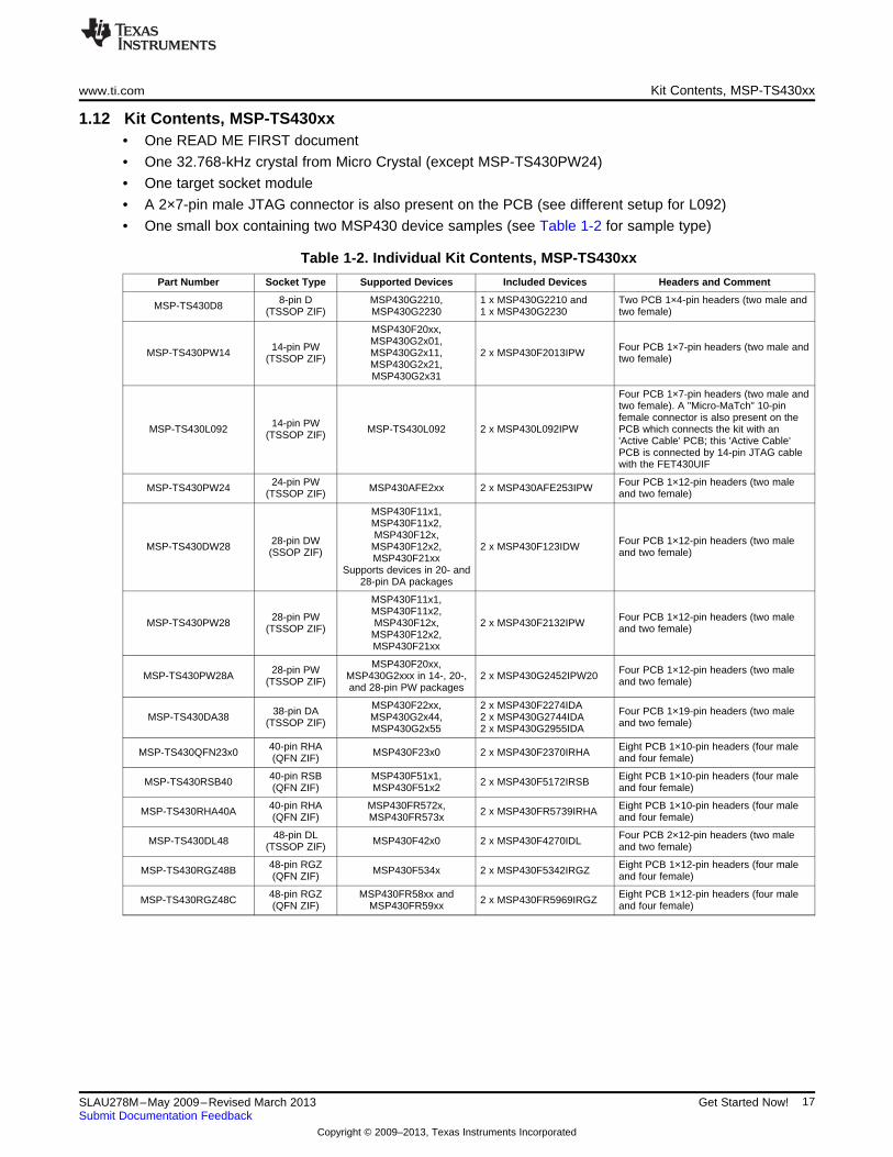
1-2. Individual Kit Contents, MSP-TS430xx ................................................................................. 17
B-1. MSP-TS430D8 Bill of Materials.......................................................................................... 35
B-2. MSP-TS430PW14 Bill of Materials...................................................................................... 38
B-3. MSP-TS430L092 Bill of Materials ....................................................................................... 41
B-4. MSP-TS430L092 JP1 Settings .......................................................................................... 43
B-5. MSP-TS430L092 Active Cable Bill of Materials ....................................................................... 44
B-6. MSP-TS430PW24 Bill of Materials...................................................................................... 47
B-7. MSP-TS430DW28 Bill of Materials...................................................................................... 50
B-8. MSP-TS430PW28 Bill of Materials ..................................................................................... 53
B-9. MSP-TS430PW28A Bill of Materials .................................................................................... 56
B-10. MSP-TS430DA38 Bill of Materials ...................................................................................... 59
B-11. MSP-TS430QFN23x0 Bill of Materials.................................................................................. 62
B-12. MSP-TS430RSB40 Bill of Materials .................................................................................... 65
B-13. MSP-TS430RHA40A Bill of Materials................................................................................... 68
B-14. MSP-TS430DL48 Bill of Materials....................................................................................... 71
B-15. MSP-TS430RGZ48B Bill of Materials................................................................................... 74
B-16. MSP-TS430RGZ48C Revision History ................................................................................. 76
B-17. MSP-TS430RGZ48C Bill of Materials .................................................................................. 77
B-18. MSP-TS430PM64 Bill of Materials ...................................................................................... 80
B-19. MSP-TS430PM64A Bill of Materials .................................................................................... 83
B-20. MSP-TS430RGC64B Bill of Materials .................................................................................. 86
B-21. MSP-TS430RGC64C Bill of Materials .................................................................................. 90
B-22. MSP-TS430RGC64USB Bill of Materials............................................................................... 93
B-23. MSP-TS430PN80 Bill of Materials ...................................................................................... 97
B-24. MSP-TS430PN80A Bill of Materials ................................................................................... 100
B-25. MSP-TS430PN80USB Bill of Materials ............................................................................... 103
B-26. MSP-TS430PZ100 Bill of Materials.................................................................................... 107
B-27. MSP-TS430PZ100A Bill of Materials.................................................................................. 110
B-28. MSP-TS430PZ100B Bill of Materials.................................................................................. 113
B-29. MSP-TS430PZ100C Bill of Materials.................................................................................. 116
B-30. MSP-TS430PZ5x100 Bill of Materials................................................................................. 120
B-31. MSP-TS430PZ100USB Bill of Materials .............................................................................. 123
B-32. MSP-TS430PEU128 Bill of Materials ................................................................................. 127
B-33. EM430F5137RF900 Bill of Materials .................................................................................. 130
B-34. EM430F6137RF900 Bill of Materials .................................................................................. 134
B-35. EM430F6147RF900 Bill of Materials .................................................................................. 138
C-1. USB VIDs and PIDs Used in MSP430 Tools......................................................................... 149
6 List of Tables SLAU278M–May 2009–Revised March 2013Submit Documentation Feedback
Copyright © 2009–2013, Texas Instruments Incorporated
PrefaceSLAU278M–May 2009–Revised March 2013
Read This First
About This Manual
This manual describes the hardware of the Texas Instruments MSP-FET430 Flash Emulation Tool (FET).The FET is the program development tool for the MSP430 ultralow-power microcontroller. Both availableinterface types, the parallel port interface and the USB interface, are described.
How to Use This Manual
Read and follow the instructions in Chapter 1. This chapter lists the contents of the FET, providesinstructions on installing the hardware and according software drivers. After you see how quick and easy itis to use the development tools, TI recommends that you read all of this manual.
This manual describes the setup and operation of the FET but does not fully describe the MSP430™microcontrollers or the development software systems. For details of these items, see the appropriate TIdocuments listed in Section 1.18.
This manual applies to the following tools (and devices):
• MSP-FET430PIF (debug interface with parallel port connection, for all MSP430 flash-based devices)
• MSP-FET430UIF (debug interface with USB connection, for all MSP430 flash-based devices)
• eZ430-F2013 (USB stick form factor interface with attached MSP430F2013 target, for allMSP430F20xx, MSP430G2x01, MSP430G2x11, MSP430G2x21, and MSP430G2x31 devices)
• eZ430-T2012 (three MSP430F2012 based target boards)
• eZ430-RF2500 (USB stick form factor interface with attached MSP430F2274 and CC2500 target, forall MSP430F20xx, MSP430F21x2, MSP430F22xx, MSP430G2x01, MSP430G2x11, MSP430G2x21,and MSP430G2x31 devices)
• eZ430-RF2500T (one MSP430F2274 and CC2500 target board including battery pack)
• eZ430-RF2500-SEH (USB stick form factor interface with attached MSP430F2274 and CC2500 targetand solar energy harvesting module)
• eZ430-Chronos-xxx (USB stick form factor interface with CC430F6137 based development systemcontained in a watch. Includes <1 GHz RF USB access point)
The following tools contain the USB debug interface (MSP-FET430UIF) and the respective target socketmodule:
• MSP-FET430U8 (for MSP430G2210 and MSP430G2230 devices in 8-pin D packages) (green PCB)
• MSP-FET430U14 (for MSP430F20xx, MSP430F20xx, MSP430G2x01, MSP430G2x11,MSP430G2x21, and MSP430G2x31 devices in 14-pin PW packages) (green PCB)
• MSP-FET430U092 (for MSP430FL092 devices in 14-pin PW packages) (green PCB)
• MSP-FET430U24 (for MSP430AFE2xx devices in 24-pin PW packages) (green PCB)
• MSP-FET430U28 (for MSP430F11xx(A) devices in 20- and 28-pin DW or PW packages)
• MSP-FET430U28A (for MSP430F20xx and MSP430G2xxx devices in 14-, 20-, and 28-pin PW)
• MSP-FET430U38 (for MSP430F22x2 and MSP430F22x4 devices in 38-pin DA packages)
• MSP-FET430U23x0 (for MSP430F23x0 devices in 40-pin RHA packages)
• MSP-FET430U40 (for MSP430F51x1, MSP430F51x2 devices in 40-pin RSB packages)
• MSP-FET430U40A (for MSP430FR572x, MSP430FR573x devices in 40-pin RHA packages)
• MSP-FET430U48 (for MSP430F22x2 and MSP430F22x4 devices in 48-pin DL packages)
• MSP-FET430U48B (for MSP430F534x devices in 48-pin RGZ packages)
7SLAU278M–May 2009–Revised March 2013 Read This FirstSubmit Documentation Feedback
Copyright © 2009–2013, Texas Instruments Incorporated
How to Use This Manual www.ti.com
• MSP-FET430U48C (for MSP430FR58xx and MSP430FR59xx devices in 48-pin RGZ packages)
• MSP-FET430U64 (for MSP430F13x, MSP430F14x, MSP430F14x1, MSP430F15x, MSP430F16x(1),MSP430F23x, MSP430F24x, MSP430F24xx, MSP430F261x, MSP430F41x, MSP430F42x(A),MSP430FE42x(A), MSP430FE42x2, and MSP430FW42x devices in 64-pin PM packages)
• MSP-FET430U64A (for MSP430F41x2 devices in 64-pin PM packages) (red PCB)
• MSP-FET430U64B (for MSP430F530x devices in 64-pin RGC packages) (blue PCB)
• MSP-FET430U64C (for MSP430F522x and MSP430F521x devices in 64-pin RGC packages) (blackPCB)
• MSP-FET430U64USB (for MSP430F550x, MSP430F551x, MSP430552x, devices in 64-pin RGCpackages)
• MSP-FET430U80 (for MSP430F241x, MSP430F261x, MSP430F43x, MSP430F43x1, MSP430FG43x,MSP430F47x, and MSP430FG47x devices in 80-pin PN packages)
• MSP-FET430U80A (for MSP430F532x devices in 80-pin PN packages)
• MSP-FET430U80USB (for MSP430F552x devices with USB peripheral in 80-pin PN packages)
• MSP-FET430U100 (for MSP430F43x, MSP430F43x1, MSP430F44x, MSP430FG461x, andMSP430F47xx devices in 100-pin PZ packages)
• MSP-FET430U100A (for MSP430F471xx devices in 100-pin PZ packages) (red PCB)
• MSP-FET430U100B (for MSP430F67xx devices in 100-pin PZ packages) (blue PCB)
• MSP-FET430U100C (for MSP430F643x and MSP430F533x devices in 100-pin PZ packages) (blackPCB)
• MSP-FET430U5x100 (for MSP430F54xx(A) devices and MSP430BT5190 in 100-pin PZ packages)(green PCB)
• MSP-FET430U100USB (for MSP430F663x and MSP430F563x devices in 100-pin PZ packages)(green PCB)
• MSP-FET430U128 (for MSP430F67xx and MSP430F67xx1 devices in 128-pin PEU packages) (greenPCB)
• FET430F5137RF900 (for CC430F513x devices in 48-pin RGZ packages) (green PCB)
• FET430F6137RF900 (for CC430F612x and CC430F613x devices in 64-pin RGC packages) (greenPCB)
Stand-alone target-socket modules (without debug interface):
• MSP-TS430D8 (for MSP430G2210 and MSP430G2230 devices in 8-pin D packages) (green PCB)
• MSP-TS430PW14 (for MSP430F20xx, MSP430G2x01, MSP430G2x11, MSP430G2x21 andMSP430G2x31 devices in 14-pin PW packages) (green PCB)
• MSP-TS430L092 (for MSP430FL092 devices in 14-pin PW packages) (green PCB)
• MSP-TS430PW24 (for MSP430AFE2xx devices in 24-pin PW packages) (green PCB)
• MSP-TS430DW28 (for MSP430F11xx(A) devices in 28-pin DW packages) (green PCB)
• MSP-TS430PW28 (for MSP430F11xx(A) devices in 28-pin PW packages) (green PCB)
• MSP-TS430PW28A (for MSP430F20xx and MSP430G2xxx devices in 14, 20, and 28-pin PW) (redPCB)
• MSP-TS430DA38 (for MSP430F22x2 and MSP430F22x4 devices in 38-pin DA packages) (green PCB)
• MSP-TS430QFN23x0 / MSP-TS430QFN40 (for MSP430F23x0 devices in 40-pin RHA packages)(green PCB)
• MSP-TS430RSB40 (for MSP430F51x1, MSP430F51x2 devices in 40-pin RSB packages) (green PCB)
• MSP-TS430RHA40A (for MSP430FR572x, MSP430FR573x devices in 40-pin RHA packages) (redPCB)
• MSP-TS430DL48 (for MSP430F22x2 and MSP430F22x4 devices in 48-pin DL packages) (green PCB)
• MSP-TS430RGZ48B (for MSP430F534x devices in 48-pin RGZ packages) (blue PCB)
• MSP-TS430RGZ48C (for MSP430FR58xx and MSP430FR59xx devices in 48-pin RGZ packages)(black PCB)
8 Read This First SLAU278M–May 2009–Revised March 2013Submit Documentation Feedback
Copyright © 2009–2013, Texas Instruments Incorporated
www.ti.com How to Use This Manual
• MSP-TS430PM64 (for MSP430F13x, MSP430F14x, MSP430F14x1, MSP430F15x, MSP430F16x(1),MSP430F23x, MSP430F24x, MSP430F24xx, MSP430F261x, MSP430F41x, MSP430F42x(A),MSP430FE42x(A), MSP430FE42x2, and MSP430FW42x devices in 64-pin PM packages) (greenPCB)
• MSP-TS430PM64A (for MSP430F41x2 devices in 64-pin PM packages) (red PCB)
• MSP-TS430RGC64B (for MSP430F530x devices in 64-pin RGC packages) (blue PCB)
• MSP-TS430RGC64C (for MSP430F522x and MSP430F521x devices in 64-pin RGC packages) (blackPCB)
• MSP-TS430RGC64USB (for MSP430F550x, MSP430F551x, MSP430F552x, devices in 64-pin RGCpackages) (green PCB)
• MSP-TS430PN80 (for MSP430F241x, MSP430F261x, MSP430F43x, MSP430F43x1, MSP430FG43x,MSP430F47x, and MSP430FG47x devices in 80-pin PN packages) (green PCB)
• MSP-TS430PN80A (for MSP430F532x devices in 80-pin PN packages) (red PCB)
• MSP-TS430PN80USB (for MSP430F551x and MSP430F552x devices with USB peripheral in 80-pinPN packages) (green PCB)
• MSP-TS430PZ100 (for MSP430F43x, MSP430F43x1, MSP430F44x, MSP430FG461x, andMSP430F47xx devices in 100-pin PZ packages) (green PCB)
• MSP-TS430PZ100A (for MSP430F471xx devices in 100-pin PZ packages) (red PCB)
• MSP-FET430PZ100B (for MSP430F67xx devices in 100-pin PZ packages) (blue PCB)
• MSP-TS430PZ100C (for MSP430F643x and MSP430F533x devices in 100-pin PZ packages) (blackPCB)
• MSP-TS430PZ5x100 (for MSP430F54xx(A) and the MSP430BT5190 devices in 100-pin PZ packages)(green PCB)
• MSP-TS430PZ100USB (for MSP430F663x and MSP430F563x devices in 100-pin PZ packages)(green PCB)
• MSP-TS430PEU128 (for MSP430F67xx and MSP430F67xx1 devices in 128-pin PEU packages)(green PCB)
• EM430F5137RF900 (with integrated CC430F5137 IC in a 48-pin RGZ package) (green PCB)
• EM430F6137RF900 (with integrated CC430F6137 IC in a 64-pin RGC package) (green PCB)
• EM430F6147RF900 (with integrated CC430F6147 IC in a 64-pin RGC package) (red PCB)
These tools contain the most up-to-date materials available at the time of packaging. For the latestmaterials (data sheets, user's guides, software, application information, etc.), visit the TI MSP430 web siteat www.ti.com/msp430 or contact your local TI sales office.
9SLAU278M–May 2009–Revised March 2013 Read This FirstSubmit Documentation Feedback
Copyright © 2009–2013, Texas Instruments Incorporated
Information About Cautions and Warnings www.ti.com
Information About Cautions and Warnings
This document may contain cautions and warnings.
CAUTION
This is an example of a caution statement.
A caution statement describes a situation that could potentially damage yoursoftware or equipment.
WARNINGThis is an example of a warning statement.
A warning statement describes a situation that could potentiallycause harm to you.
The information in a caution or a warning is provided for your protection. Read each caution and warningcarefully.
Related Documentation From Texas Instruments
MSP430 development tools documentation:
CCS for MSP430 User's Guide (literature number SLAU157)
Code Composer Studio v5.x Core Edition (CCS Mediawiki)
IAR for MSP430 User's Guide (literature number SLAU138)
IAR Embedded Workbench KickStart (literature number SLAC050)
eZ430-F2013 Development Tool User's Guide (literature number SLAU176)
eZ430-RF2480 User's Guide (literature number SWRA176)
eZ430-RF2500 Development Tool User's Guide (literature number SLAU227)
eZ430-RF2500-SEH Development Tool User's Guide (literature number SLAU273)
eZ430-Chronos Development Tool User's Guide (literature number SLAU292)
MSP-SA430SUB1GHZ, Sub-1 GHz RF Spectrum Analyzer Tool (literature number SLAU371)
MSP430F5529 USB Experimenter’s Board, MSP-EXP430F5529 (literature number SLAU330)
MSP430F5438 Experimenter Board, MSP-EXP430F5438 (literature number SLAU263)
MSP430 LaunchPad Value Line Development kit, MSP-EXP430G2 (literature number SLAU318)
MSP430 device user's guides:
MSP430x1xx Family User's Guide (literature number SLAU049)
MSP430x2xx Family User's Guide (literature number SLAU144)
MSP430x3xx Family User's Guide (literature number SLAU012)
MSP430x4xx Family User's Guide (literature number SLAU056)
MSP430x5xx and MSP430x6xx Family User's Guide (literature number SLAU208)
CC430 Family User's Guide (literature number SLAU259)
MSP430FR57xx Family User's Guide (literature number SLAU272)
MSP430FR58xx and MSP430FR59xx Family User's Guide (literature number SLAU367)
10 Read This First SLAU278M–May 2009–Revised March 2013Submit Documentation Feedback
Copyright © 2009–2013, Texas Instruments Incorporated
www.ti.com If You Need Assistance
If You Need Assistance
Support for the MSP430 devices and the FET development tools is provided by the Texas InstrumentsProduct Information Center (PIC). Contact information for the PIC can be found on the TI web site atwww.ti.com/support. The Texas Instruments E2E Community support forums for the MSP430 provideopen interaction with peer engineers, TI engineers, and other experts. Additional device-specificinformation can be found on the MSP430 web site.
11SLAU278M–May 2009–Revised March 2013 Read This FirstSubmit Documentation Feedback
Copyright © 2009–2013, Texas Instruments Incorporated
Chapter 1SLAU278M–May 2009–Revised March 2013
Get Started Now!
This chapter lists the contents of the FET and provides instruction on installing the hardware.
Topic ........................................................................................................................... Page
1.1 Flash Emulation Tool (FET) Overview .................................................................. 131.2 Kit Contents, MSP-FET430PIF ............................................................................. 141.3 Kit Contents, eZ430-F2013 .................................................................................. 141.4 Kit Contents, eZ430-T2012 .................................................................................. 141.5 Kit Contents, eZ430-RF2500 ................................................................................ 141.6 Kit Contents, eZ430-RF2500T .............................................................................. 141.7 Kit Contents, eZ430-RF2500-SEH ........................................................................ 141.8 Kit Contents, eZ430-Chronos-xxx ........................................................................ 151.9 Kit Contents, MSP-FET430UIF ............................................................................. 151.10 Kit Contents, MSP-FET430xx .............................................................................. 151.11 Kit Contents, FET430F6137RF900 ........................................................................ 161.12 Kit Contents, MSP-TS430xx ................................................................................ 171.13 Kit Contents, EM430Fx1x7RF900 ......................................................................... 191.14 Hardware Installation, MSP-FET430PIF ................................................................ 191.15 Hardware Installation, MSP-FET430UIF ................................................................ 191.16 Hardware Installation, eZ430-XXXX, MSP-EXP430G2, MSP-EXP430FR5739, MSP-
EXP430F5529 .................................................................................................... 201.17 Hardware Installation, MSP-FET430Uxx, MSP-TS430xxx, FET430F6137RF900,
EM430Fx137RF900 ............................................................................................ 201.18 Important MSP430 Documents on the Web ........................................................... 20
12 Get Started Now! SLAU278M–May 2009–Revised March 2013Submit Documentation Feedback
Copyright © 2009–2013, Texas Instruments Incorporated
www.ti.com Flash Emulation Tool (FET) Overview
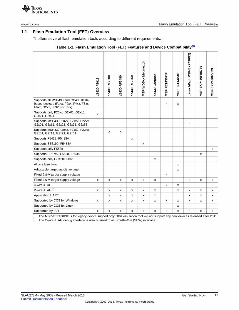
1.1 Flash Emulation Tool (FET) Overview
TI offers several flash emulation tools according to different requirements.
Table 1-1. Flash Emulation Tool (FET) Features and Device Compatibility (1)
eZ43
0-F
2013
eZ43
0-R
F25
00
eZ43
0-R
F24
80
eZ43
0-R
F25
60
MS
P-W
DS
xxM
etaw
atch
eZ43
0-C
hro
no
s
MS
P-F
ET
430P
IF
MS
P-F
ET
430U
IF
Lau
nch
Pad
(MS
P-E
XP
430G
2)
MS
P-E
XP
430F
R57
39
MS
P-E
XP
430F
5529
Supports all MSP430 and CC430 flash-based devices (F1xx, F2xx, F4xx, F5xx, x xF6xx, G2xx, L092, FR57xx)
Supports only F20xx, G2x01, G2x11, xG2x21, G2x31
Supports MSP430F20xx, F21x2, F22xx, xG2x01, G2x11, G2x21, G2x31, G2x53
Supports MSP430F20xx, F21x2, F22xx, x xG2x01, G2x11, G2x21, G2x31
Supports F5438, F5438A x
Supports BT5190, F5438A x
Supports only F552x x
Supports FR57xx, F5638, F6638 x
Supports only CC430F613x x
Allows fuse blow x
Adjustable target supply voltage x
Fixed 2.8-V target supply voltage x
Fixed 3.6-V target supply voltage x x x x x x x x x
4-wire JTAG x x
2-wire JTAG (2) x x x x x x x x x x
Application UART x x x x x x x x
Supported by CCS for Windows x x x x x x x x x x x
Supported by CCS for Linux x
Supported by IAR x x x x x x x x x x x(1) The MSP-FET430PIF is for legacy device support only. This emulation tool will not support any new devices released after 2011.(2) The 2-wire JTAG debug interface is also referred to as Spy-Bi-Wire (SBW) interface.
13SLAU278M–May 2009–Revised March 2013 Get Started Now!Submit Documentation Feedback
Copyright © 2009–2013, Texas Instruments Incorporated
Kit Contents, MSP-FET430PIF www.ti.com
1.2 Kit Contents, MSP-FET430PIF• One READ ME FIRST document
• One MSP-FET430PIF interface module
• One 25-conductor cable
• One 14-conductor cable
NOTE: This part is obsolete and is not recommended to use in new design.
1.3 Kit Contents, eZ430-F2013• One QUICK START GUIDE document
• One eZ430-F2013 development tool including one MSP430F2013 target board
1.4 Kit Contents, eZ430-T2012• Three MSP430F2012-based target boards
1.5 Kit Contents, eZ430-RF2500• One QUICK START GUIDE document
• One eZ430-RF2500 CD-ROM
• One eZ430-RF2500 development tool including one MSP430F2274 and CC2500 target board
• One eZ430-RF2500T target board
• One AAA battery pack with expansion board (batteries included)
1.6 Kit Contents, eZ430-RF2500T• One eZ430-RF2500T target board
• One AAA battery pack with expansion board (batteries included)
1.7 Kit Contents, eZ430-RF2500-SEH• One MSP430 development tool CD containing documentation and development software
• One eZ430-RF USB debugging interface
• Two eZ430-RF2500T wireless target boards
• One SEH-01 solar energy harvester board
• One AAA battery pack with expansion board (batteries included)
14 Get Started Now! SLAU278M–May 2009–Revised March 2013Submit Documentation Feedback
Copyright © 2009–2013, Texas Instruments Incorporated
www.ti.com Kit Contents, eZ430-Chronos-xxx
1.8 Kit Contents, eZ430-Chronos-xxx
'433, '868, '915• One QUICK START GUIDE document
• One ez430-Chronos emulator
• One screwdriver
• Two spare screws
eZ430-Chronos-433:– One 433-MHz eZ430-Chronos watch (battery included)
– One 433-MHz eZ430-Chronos access point
eZ430-Chronos-868:– One 868-MHz eZ430-Chronos watch (battery included)
– One 868-MHz eZ430-Chronos access point
eZ430-Chronos-915:– One 915-MHz eZ430-Chronos watch (battery included)
– One 915-MHz eZ430-Chronos access point
1.9 Kit Contents, MSP-FET430UIF• One READ ME FIRST document
• One MSP-FET430UIF interface module
• One USB cable
• One 14-conductor cable
1.10 Kit Contents, MSP-FET430xx
'U8, 'U14, 'U092, 'U24, 'U28, 'U28A, 'U38, 'U23x0, 'U40, 'U40A, 'U48, 'U48B, 'U64, 'U64A, 'U64B,'U64C, 'U64USB, 'U80, 'U80USB, 'U100, 'U100A, 'U100B, 'U100C, 'U5x100, 'U100USB, 'U128• One READ ME FIRST document
• One MSP-FET430UIF USB interface module. This is the unit that has a USB B-connector on one endof the case, and a 2×7-pin male connector on the other end of the case.
• One USB cable
• One 32.768-kHz crystal from Micro Crystal (except MSP-FET430U24)
• A 2×7-pin male JTAG connector is also present on the PCB (see different setup for L092)
• One 14-Pin JTAG conductor cable
• One small box containing two MSP430 device samples (See table for Sample Type)
• One target socket module. To check the devices used for each board and a summary of the board,see Table 1-2. MSP-TS430xx below is the target socket module for each MSP-FET430Uxx kit.
MSP-FET430U8: One MSP-TS430D8 target socket module.
MSP-FET430U14: One MSP-TS430PW14 target socket module.
MSP-FET430U092: One MSP-TS430L092 target socket module with Active Cable.
MSP-FET430U24: One MSP-TS430PW24 target socket module.
MSP-FET430U28: One MSP-TS430PW28 target socket module.
MSP-FET430U28A: One MSP-TS430PW28A target socket module.
MSP-FET430U38: One MSP-TS430DA38 target socket module..
MSP-FET430U23x0: One MSP-TS430QFN23x0 (former name MSP-TS430QFN40) target socketmodule.
MSP-FET430U40: One MSP-TS430RSB40 target socket module.
MSP-FET430U48: One MSP-TS430DL48 target socket module.
15SLAU278M–May 2009–Revised March 2013 Get Started Now!Submit Documentation Feedback
Copyright © 2009–2013, Texas Instruments Incorporated
Kit Contents, FET430F6137RF900 www.ti.com
MSP-FET430U48B: One MSP-TS430RGZ48B target socket module.
MSP-FET430U48C: One MSP-TS430RGZ48C target socket module.
MSP-FET430U64: One MSP-TS430PM64 target socket module.
MSP-FET430U64A: One MSP-TS430PM64A target socket module.
MSP-FET430U64B: One MSP-TS430RGC64B target socket module.
MSP-FET430U64C: One MSP-TS430RGC64C target socket module.
MSP-FET430U64USB: One MSP-TS430RGC64USB target socket module.
MSP-FET430U80: One MSP-TS430PN80 target socket module.
MSP-FET430U80A: One MSP-TS430PN80A target socket module.
MSP-FET430U80USB: One MSP-TS430PN80USB target socket module.
MSP-FET430U100: One MSP-TS430PZ100 target socket module.
MSP-FET430U100A: One MSP-TS430PZ100A target socket module.
MSP-FET430U100B: One MSP-TS430PZ100B target socket module.
MSP-FET430U100C: One MSP-TS430PZ100C target socket module.
MSP-FET430U5x100: One MSP-TS430PZ5x100 target socket module.
MSP-FET430U100USB: One MSP-TS430PZ100USB target socket module.
MSP-FET430U128: One MSP-TS430PEU128 target socket module.
Consult the device data sheets for device specifications. Device errata can be found in the respectivedevice product folder on the web provided as a PDF document. Depending on the device, errata may alsobe found in the device bug database at www.ti.com/sc/cgi-bin/buglist.cgi.
1.11 Kit Contents, FET430F6137RF900• One READ ME FIRST document
• One legal notice
• One MSP-FET430UIF interface module
• Two EM430F6137RF900 target socket modules. This is the PCB on which is soldered a CC430F6137device in a 64-pin RGC package. A 2×7-pin male connector is also present on the PCB
• Two CC430EM battery packs
• Four AAA batteries
• Two 868-MHz or 915-MHz antennas
• Two 32.768-kHz crystals
• 18 PCB 2x4-pin headers
• One USB cable
• One 14-pin JTAG conductor cable
16 Get Started Now! SLAU278M–May 2009–Revised March 2013Submit Documentation Feedback
Copyright © 2009–2013, Texas Instruments Incorporated
www.ti.com Kit Contents, MSP-TS430xx
1.12 Kit Contents, MSP-TS430xx• One READ ME FIRST document
• One 32.768-kHz crystal from Micro Crystal (except MSP-TS430PW24)
• One target socket module
• A 2×7-pin male JTAG connector is also present on the PCB (see different setup for L092)
• One small box containing two MSP430 device samples (see Table 1-2 for sample type)
Table 1-2. Individual Kit Contents, MSP-TS430xx
Part Number Socket Type Supported Devices Included Devices Headers and Comment
8-pin D MSP430G2210, 1 x MSP430G2210 and Two PCB 1×4-pin headers (two male andMSP-TS430D8 (TSSOP ZIF) MSP430G2230 1 x MSP430G2230 two female)
MSP430F20xx,MSP430G2x01,14-pin PW Four PCB 1×7-pin headers (two male andMSP-TS430PW14 MSP430G2x11, 2 x MSP430F2013IPW(TSSOP ZIF) two female)MSP430G2x21,MSP430G2x31
Four PCB 1×7-pin headers (two male andtwo female). A "Micro-MaTch" 10-pinfemale connector is also present on the14-pin PWMSP-TS430L092 MSP-TS430L092 2 x MSP430L092IPW PCB which connects the kit with an(TSSOP ZIF) 'Active Cable' PCB; this 'Active Cable'PCB is connected by 14-pin JTAG cablewith the FET430UIF
24-pin PW Four PCB 1×12-pin headers (two maleMSP-TS430PW24 MSP430AFE2xx 2 x MSP430AFE253IPW(TSSOP ZIF) and two female)
MSP430F11x1,MSP430F11x2,MSP430F12x,28-pin DW Four PCB 1×12-pin headers (two maleMSP-TS430DW28 MSP430F12x2, 2 x MSP430F123IDW(SSOP ZIF) and two female)MSP430F21xx
Supports devices in 20- and28-pin DA packages
MSP430F11x1,MSP430F11x2,28-pin PW Four PCB 1×12-pin headers (two maleMSP-TS430PW28 MSP430F12x, 2 x MSP430F2132IPW(TSSOP ZIF) and two female)MSP430F12x2,MSP430F21xx
MSP430F20xx,28-pin PW Four PCB 1×12-pin headers (two maleMSP-TS430PW28A MSP430G2xxx in 14-, 20-, 2 x MSP430G2452IPW20(TSSOP ZIF) and two female)and 28-pin PW packages
MSP430F22xx, 2 x MSP430F2274IDA38-pin DA Four PCB 1×19-pin headers (two maleMSP-TS430DA38 MSP430G2x44, 2 x MSP430G2744IDA(TSSOP ZIF) and two female)MSP430G2x55 2 x MSP430G2955IDA
40-pin RHA Eight PCB 1×10-pin headers (four maleMSP-TS430QFN23x0 MSP430F23x0 2 x MSP430F2370IRHA(QFN ZIF) and four female)
40-pin RSB MSP430F51x1, Eight PCB 1×10-pin headers (four maleMSP-TS430RSB40 2 x MSP430F5172IRSB(QFN ZIF) MSP430F51x2 and four female)
40-pin RHA MSP430FR572x, Eight PCB 1×10-pin headers (four maleMSP-TS430RHA40A 2 x MSP430FR5739IRHA(QFN ZIF) MSP430FR573x and four female)
48-pin DL Four PCB 2×12-pin headers (two maleMSP-TS430DL48 MSP430F42x0 2 x MSP430F4270IDL(TSSOP ZIF) and two female)
48-pin RGZ Eight PCB 1×12-pin headers (four maleMSP-TS430RGZ48B MSP430F534x 2 x MSP430F5342IRGZ(QFN ZIF) and four female)
48-pin RGZ MSP430FR58xx and Eight PCB 1×12-pin headers (four maleMSP-TS430RGZ48C 2 x MSP430FR5969IRGZ(QFN ZIF) MSP430FR59xx and four female)
17SLAU278M–May 2009–Revised March 2013 Get Started Now!Submit Documentation Feedback
Copyright © 2009–2013, Texas Instruments Incorporated
Kit Contents, MSP-TS430xx www.ti.com
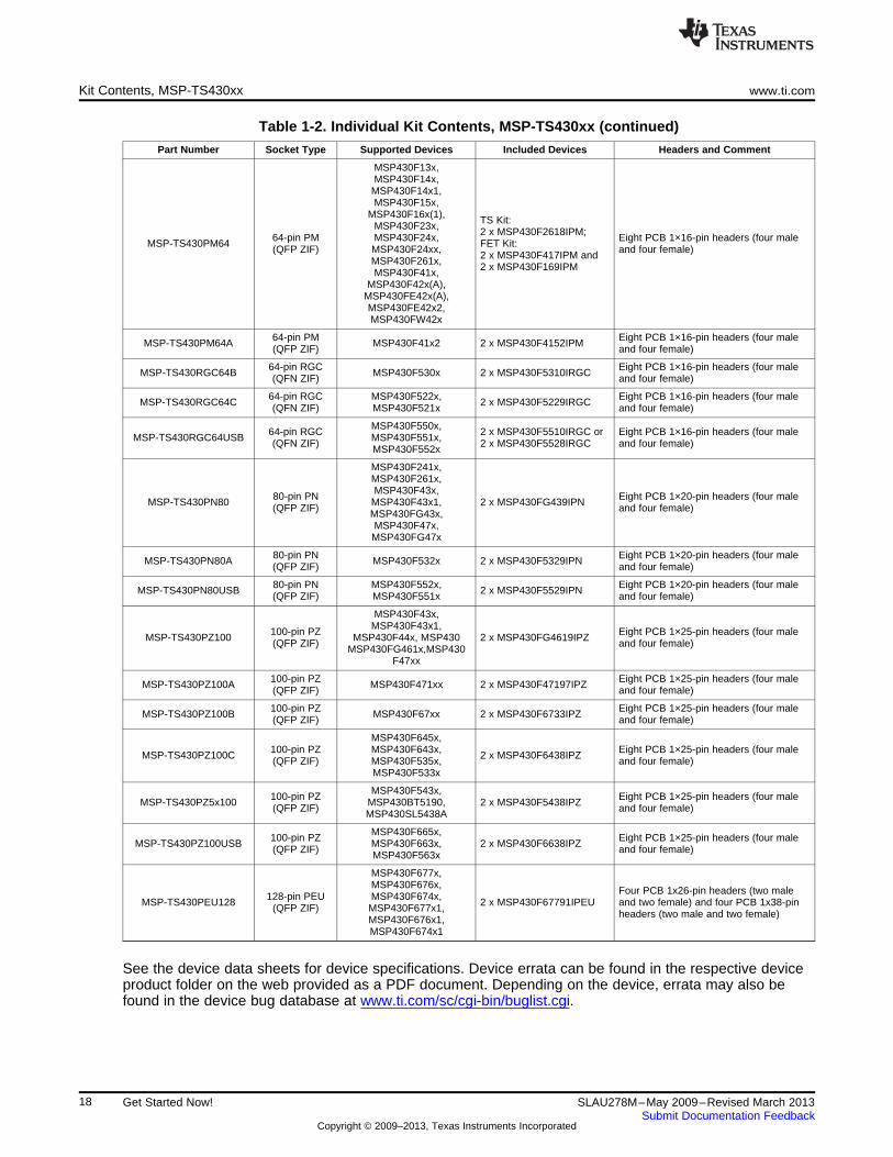
Table 1-2. Individual Kit Contents, MSP-TS430xx (continued)
Part Number Socket Type Supported Devices Included Devices Headers and Comment
MSP430F13x,MSP430F14x,
MSP430F14x1,MSP430F15x,
MSP430F16x(1), TS Kit:MSP430F23x, 2 x MSP430F2618IPM;64-pin PM MSP430F24x, Eight PCB 1×16-pin headers (four maleMSP-TS430PM64 FET Kit:(QFP ZIF) MSP430F24xx, and four female)2 x MSP430F417IPM andMSP430F261x, 2 x MSP430F169IPMMSP430F41x,MSP430F42x(A),
MSP430FE42x(A),MSP430FE42x2,MSP430FW42x
64-pin PM Eight PCB 1×16-pin headers (four maleMSP-TS430PM64A MSP430F41x2 2 x MSP430F4152IPM(QFP ZIF) and four female)
64-pin RGC Eight PCB 1×16-pin headers (four maleMSP-TS430RGC64B MSP430F530x 2 x MSP430F5310IRGC(QFN ZIF) and four female)
64-pin RGC MSP430F522x, Eight PCB 1×16-pin headers (four maleMSP-TS430RGC64C 2 x MSP430F5229IRGC(QFN ZIF) MSP430F521x and four female)
MSP430F550x,64-pin RGC 2 x MSP430F5510IRGC or Eight PCB 1×16-pin headers (four maleMSP-TS430RGC64USB MSP430F551x,(QFN ZIF) 2 x MSP430F5528IRGC and four female)MSP430F552x
MSP430F241x,MSP430F261x,MSP430F43x,80-pin PN Eight PCB 1×20-pin headers (four maleMSP-TS430PN80 MSP430F43x1, 2 x MSP430FG439IPN(QFP ZIF) and four female)MSP430FG43x,MSP430F47x,MSP430FG47x
80-pin PN Eight PCB 1×20-pin headers (four maleMSP-TS430PN80A MSP430F532x 2 x MSP430F5329IPN(QFP ZIF) and four female)
80-pin PN MSP430F552x, Eight PCB 1×20-pin headers (four maleMSP-TS430PN80USB 2 x MSP430F5529IPN(QFP ZIF) MSP430F551x and four female)
MSP430F43x,MSP430F43x1,100-pin PZ Eight PCB 1×25-pin headers (four maleMSP-TS430PZ100 MSP430F44x, MSP430 2 x MSP430FG4619IPZ(QFP ZIF) and four female)MSP430FG461x,MSP430
F47xx
100-pin PZ Eight PCB 1×25-pin headers (four maleMSP-TS430PZ100A MSP430F471xx 2 x MSP430F47197IPZ(QFP ZIF) and four female)
100-pin PZ Eight PCB 1×25-pin headers (four maleMSP-TS430PZ100B MSP430F67xx 2 x MSP430F6733IPZ(QFP ZIF) and four female)
MSP430F645x,100-pin PZ MSP430F643x, Eight PCB 1×25-pin headers (four maleMSP-TS430PZ100C 2 x MSP430F6438IPZ(QFP ZIF) MSP430F535x, and four female)
MSP430F533x
MSP430F543x,100-pin PZ Eight PCB 1×25-pin headers (four maleMSP-TS430PZ5x100 MSP430BT5190, 2 x MSP430F5438IPZ(QFP ZIF) and four female)MSP430SL5438A
MSP430F665x,100-pin PZ Eight PCB 1×25-pin headers (four maleMSP-TS430PZ100USB MSP430F663x, 2 x MSP430F6638IPZ(QFP ZIF) and four female)MSP430F563x
MSP430F677x,MSP430F676x, Four PCB 1x26-pin headers (two male128-pin PEU MSP430F674x,MSP-TS430PEU128 2 x MSP430F67791IPEU and two female) and four PCB 1x38-pin(QFP ZIF) MSP430F677x1, headers (two male and two female)MSP430F676x1,MSP430F674x1
See the device data sheets for device specifications. Device errata can be found in the respective deviceproduct folder on the web provided as a PDF document. Depending on the device, errata may also befound in the device bug database at www.ti.com/sc/cgi-bin/buglist.cgi.
18 Get Started Now! SLAU278M–May 2009–Revised March 2013Submit Documentation Feedback
Copyright © 2009–2013, Texas Instruments Incorporated
www.ti.com Kit Contents, EM430Fx1x7RF900
1.13 Kit Contents, EM430Fx1x7RF900• One READ ME FIRST document
• One legal notice
• Two target socket module
MSP-EM430F5137RF900: Two EM430F5137RF900 target socket modules. This is the PCB on whichis soldered a CC430F5137 device in a 48-pin RGZ package. A 2×7-pin male connector is also presenton the PCB
MSP-EM430F6137RF900: Two EM430F6137RF900 target socket modules. This is the PCB on whichis soldered a CC430F6137 device in a 64-pin RGC package. A 2×7-pin male connector is also presenton the PCB
MSP-EM430F6147RF900: Two EM430F6147RF900 target socket modules. This is the PCB on whichis soldered a CC430F6147 device in a 64-pin RGC package. A 2×7-pin male connector is also presenton the PCB
• Two CC430EM battery packs
• Four AAA batteries
• Two 868- or 915-MHz antennas
• Two 32.768-kHz crystals
• 18 PCB 2×4-pin headers
1.14 Hardware Installation, MSP-FET430PIF
Follow these steps to install the hardware for the MSP-FET430PIF tools:
1. Use the 25-conductor cable to connect the FET interface module to the parallel port of the PC. Thenecessary driver for accessing the PC parallel port is installed automatically during CCS or IAREmbedded Workbench installation. Note that a restart is required after the CCS or IAR EmbeddedWorkbench installation for the driver to become active.
2. Use the 14-conductor cable to connect the parallel-port debug interface module to a target board, suchas an MSP-TS430xxx target socket module. Module schematics and PCBs are shown in Appendix B.
1.15 Hardware Installation, MSP-FET430UIF
Follow these steps to install the hardware for the MSP-FET430UIF tool:
1. Install the IDE (CCS or IAR) you plan to use before connecting USB-FET interface to PC. The IDEinstallation installs drivers automatically.
2. Use the USB cable to connect the USB-FET interface module to a USB port on the PC. The USB FETshould be recognized, as the USB device driver is installed automatically. If the driver has not beeninstalled yet, the install wizard starts. Follow the prompts and point the wizard to the driver files.
The default location for CCS is c:\ti\ccsv5\ccs_base\emulation\drivers\msp430\USB_CDC orc:\ti\ccsv5\ccs_base\emulation\drivers\msp430\USB_FET_XP_XX, depending of firmware version ofthe tool.
The default location for IAR Embedded Workbench is <Installation Root>\Embedded Workbench x.x\430\drivers\TIUSBFET\eZ430-UART or <Installation Root>\Embedded Workbench x.x\430\drivers\<Win_OS>, depending of firmware version of the tool.
The USB driver is installed automatically. Detailed driver installation instructions can be found inAppendix C.
3. After connecting to a PC, the USB FET performs a self-test during which the red LED may flash forapproximately two seconds. If the self-test passes successfully, the green LED stays on.
4. Use the 14-conductor cable to connect the USB-FET interface module to a target board, such as anMSP-TS430xxx target socket module.
5. Ensure that the MSP430 device is securely seated in the socket, and that its pin 1 (indicated with acircular indentation on the top surface) aligns with the "1" mark on the PCB.
6. Compared to the parallel-port debug interface, the USB FET has additional features including JTAGsecurity fuse blow and adjustable target VCC (1.8 V to 3.6 V). Supply the module with up to 60 mA.
19SLAU278M–May 2009–Revised March 2013 Get Started Now!Submit Documentation Feedback
Copyright © 2009–2013, Texas Instruments Incorporated
Hardware Installation, eZ430-XXXX, MSP-EXP430G2, MSP-EXP430FR5739, MSP-EXP430F5529 www.ti.com
1.16 Hardware Installation, eZ430-XXXX, MSP-EXP430G2, MSP-EXP430FR5739, MSP-EXP430F5529
To install eZ430-XXXX, MSP-EXP430G2, MSP-EXP430FR5739, MSP-EXP430F5529 tools followinstructions 1 and 2 of Section 1.15
1.17 Hardware Installation, MSP-FET430Uxx, MSP-TS430xxx, FET430F6137RF900,EM430Fx137RF900
Follow these steps to install the hardware for the MSP-FET430Uxx and MSP-TS430xxx tools:
1. Follow instructions 1 and 2 of Section 1.15
2. Connect the MSP-FET430PIF or MSP-FET430UIF debug interface to the appropriate port of the PC.Use the 14-conductor cable to connect the FET interface module to the supplied target socket module.
3. Ensure that the MSP430 device is securely seated in the socket and that its pin 1 (indicated with acircular indentation on the top surface) aligns with the "1" mark on the PCB.
4. Ensure that the two jumpers (LED and VCC) near the 2×7-pin male connector are in place. Illustrationsof the target socket modules and their parts are found in Appendix B.
1.18 Important MSP430 Documents on the Web
The primary sources of MSP430 information are the device-specific data sheet and user's guide. TheMSP430 web site (www.ti.com/msp430) contains the most recent version of these documents.
PDF documents describing the CCS tools (CCS IDE, the assembler, the C compiler, the linker, and thelibrarian) are in the msp430\documentation folder. A Code Composer Studio specific Wiki page (FAQ) isavailable, and the Texas Instruments E2E Community support forums for the MSP430 and CodeComposer Studio v5 provide additional help besides the product help and Welcome page.
PDF documents describing the IAR tools (Workbench C-SPY, the assembler, the C compiler, the linker,and the librarian) are in the common\doc and 430\doc folders. Supplements to the documents (that is, thelatest information) are available in HTML format in the same directories. A IAR specific Wiki Page is alsoavailable.
20 Get Started Now! SLAU278M–May 2009–Revised March 2013Submit Documentation Feedback
Copyright © 2009–2013, Texas Instruments Incorporated
Chapter 2SLAU278M–May 2009–Revised March 2013
Design Considerations for In-Circuit Programming
This chapter presents signal requirements for in-circuit programming of the MSP430.
Topic ........................................................................................................................... Page
2.1 Signal Connections for In-System Programming and Debugging ............................ 222.2 External Power .................................................................................................. 262.3 Bootstrap Loader (BSL) ..................................................................................... 26
21SLAU278M–May 2009–Revised March 2013 Design Considerations for In-Circuit ProgrammingSubmit Documentation Feedback
Copyright © 2009–2013, Texas Instruments Incorporated
Signal Connections for In-System Programming and Debugging www.ti.com
2.1 Signal Connections for In-System Programming and Debugging
MSP-FET430PIF, MSP-FET430UIF, MSP-GANG, MSP-GANG430, MSP-PRGS430
With the proper connections, the debugger and an FET hardware JTAG interface (such as the MSP-FET430PIF and MSP-FET430UIF) can be used to program and debug code on the target board. Inaddition, the connections also support the MSP-GANG430 or MSP-PRGS430 production programmers,thus providing an easy way to program prototype boards, if desired.
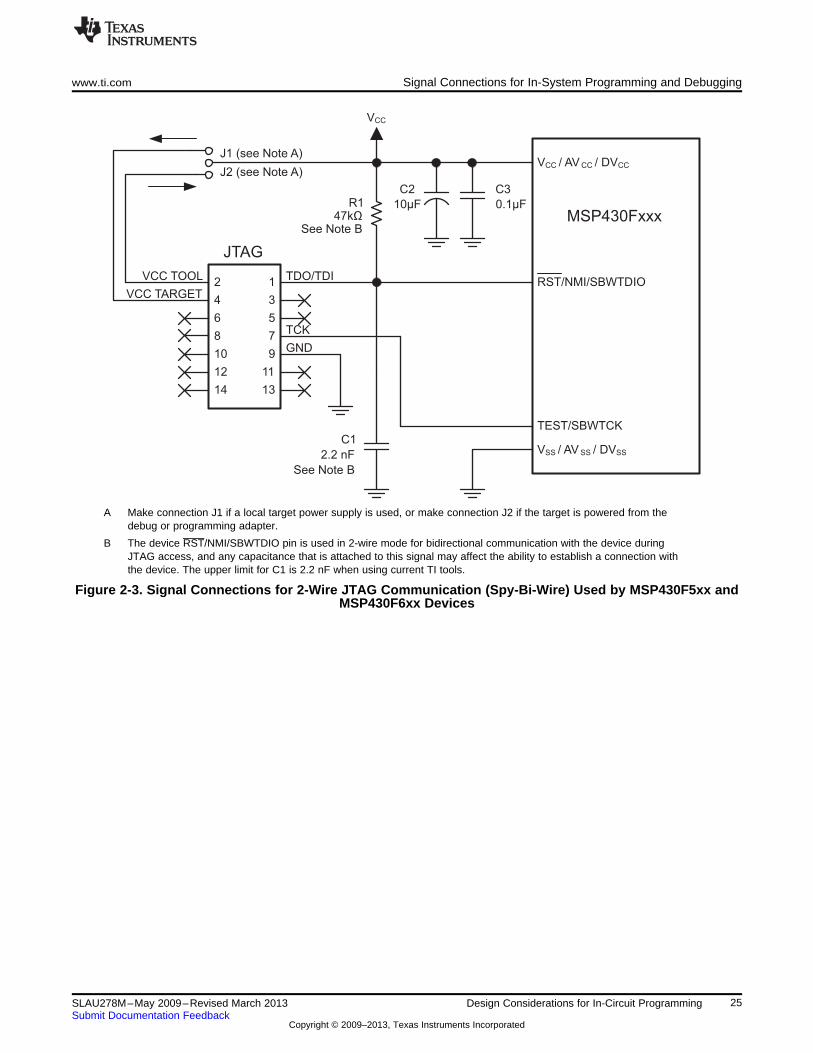
Figure 2-1 shows the connections between the 14-pin FET interface module connector and the targetdevice required to support in-system programming and debugging for 4-wire JTAG communication.Figure 2-2 shows the connections for 2-wire JTAG mode (Spy-Bi-Wire). The 4-wire JTAG mode issupported on most MSP430 devices except of small pin count devices e.g. MSP430G2230. The 2-wireJTAG mode is available on selected devices only. See the CCS User's Guide for MSP430 (SLAU157) orIAR for MSP430 User's Guide (SLAU138) for information on which interface method can be used on whichdevice.
The connections for the FET interface module and the MSP-GANG, MSP-GANG430 or MSP-PRGS430are identical. Both the FET interface module and MSP-GANG430 can supply VCC to the target board (viapin 2). In addition, the FET interface module, MSP-GANG and MSP-GANG430 have a VCC-sense featurethat, if used, requires an alternate connection (pin 4 instead of pin 2). The VCC-sense feature senses thelocal VCC present on the target board (that is, a battery or other local power supply) and adjusts the outputsignals accordingly. If the target board is to be powered by a local VCC, then the connection to pin 4 on theJTAG should be made, and not the connection to pin 2. This utilizes the VCC-sense feature and preventsany contention that might occur if the local on-board VCC were connected to the VCC supplied from the FETinterface module, MSP-GANG or the MSP-GANG430. If the VCC-sense feature is not necessary (that is, ifthe target board is to be powered from the FET interface module, MSP-GANG or MSP-GANG430), theVCC connection is made to pin 2 on the JTAG header and no connection is made to pin 4. Figure 2-1 andFigure 2-2 show a jumper block that supports both scenarios of supplying VCC to the target board. If thisflexibility is not required, the desired VCC connections may be hard-wired eliminating the jumper block. Pins2 and 4 must not be connected simultaneously.
Note that in 4-wire JTAG communication mode (see Figure 2-1), the connection of the target RST signalto the JTAG connector is optional when using devices that support only 4-wire JTAG communicationmode. However, when using devices that support 2-wire JTAG communication mode in 4-wire JTAGmode, the RST connection must be made. The MSP430 development tools and device programmersperform a target reset by issuing a JTAG command to gain control over the device. However, if this isunsuccessful, the RST signal of the JTAG connector may be used by the development tool or deviceprogrammer as an additional way to assert a device reset.
22 Design Considerations for In-Circuit Programming SLAU278M–May 2009–Revised March 2013Submit Documentation Feedback
Copyright © 2009–2013, Texas Instruments Incorporated
1
3
5
7
9
11
13
2
4
6
8
10
12
14
TDO/TDI
TDI/VPP
TMS
TCK
GND
TEST/VPP
JTAG
VCC TOOL
VCC TARGET
J1 (see Note A)
J2 (see Note A)
VCC
R1
47 k
(see Note B)
W
C2
10 µF
C3
0.1 µF
V /AV /DVCCCC CC
RST/NMI
TDO/TDI
TDI/VPP
TMS
TCK
TEST/VPP (see Note C)
V /AV /DVSS SS SS
MSP430Fxxx
C1
10 nF/2.2 nF
(see Notes B and E)
RST (see Note D)
www.ti.com Signal Connections for In-System Programming and Debugging
A If a local target power supply is used, make connection J1. If power from the debug or programming adapter is used,make connection J2.
B The configuration of R1 and C1 for the RST/NMI pin depends on the device family. See the respective MSP430 familyuser's guide for the recommended configuration.
C The TEST pin is available only on MSP430 family members with multiplexed JTAG pins. See the device-specific datasheet to determine if this pin is available.
D The connection to the JTAG connector RST pin is optional when using 4-wire JTAG communication mode capable-only devices and not required for device programming or debugging. However, this connection is required when using2-wire JTAG communication mode capable devices in 4-wire JTAG mode.
E When using 2-wire JTAG communication capable devices in 4-wire JTAG mode, the upper limit for C1 should notexceed 2.2 nF. This applies to both TI FET interface modules (LPT and USB FET).
Figure 2-1. Signal Connections for 4-Wire JTAG Communication
23SLAU278M–May 2009–Revised March 2013 Design Considerations for In-Circuit ProgrammingSubmit Documentation Feedback
Copyright © 2009–2013, Texas Instruments Incorporated
1
3
5
7
9
11
13
2
4
6
8
10
12
14
VCC / AV CC / DVCC
VSS / AV SS / DVSS
TEST/SBWTCK
MSP430Fxxx
RST/NMI/SBWTDIO
10μF 0.1μF47kΩ
TDO/TDI
TCK
GND
TEST/VPP
VCC
JTAG
R1
VCC TOOL
VCC TARGET
2.2 nF
See Note B
C1
C2 C3
330Ω
R2
J1 (see Note A)
J2 (see Note A)
See Note B
Signal Connections for In-System Programming and Debugging www.ti.com
A If a local target power supply is used, make connection J1. If power from the debug or programming adapter is used,make connection J2.
B The device RST/NMI/SBWTDIO pin is used in 2-wire mode for bidirectional communication with the device duringJTAG access, and any capacitance that is attached to this signal may affect the ability to establish a connection withthe device. The upper limit for C1 is 2.2 nF when using current TI tools.
C R2 protects the JTAG debug interface TCK signal from the JTAG security fuse blow voltage that is supplied by theTEST/VPP pin during the fuse blow process. If fuse blow functionality is not needed, R2 is not required (populate 0 Ω)and do not connect TEST/VPP to TEST/SBWTCK.
Figure 2-2. Signal Connections for 2-Wire JTAG Communication (Spy-Bi-Wire) Used by MSP430F2xx,MSP430G2xx and MSP430F4xx Devices
24 Design Considerations for In-Circuit Programming SLAU278M–May 2009–Revised March 2013Submit Documentation Feedback
Copyright © 2009–2013, Texas Instruments Incorporated
1
3
5
7
9
11
13
2
4
6
8
10
12
14
VCC / AV CC / DVCC
VSS / AV SS / DVSS
TEST/SBWTCK
MSP430Fxxx
RST/NMI/SBWTDIO
10µF 0.1μF47kΩ
TDO/TDI
TCK
GND
VCC
JTAG
R1
VCC TOOL
VCC TARGET
C1
C2 C3
J1 (see Note A)
J2 (see Note A)
2.2 nF
See Note B
See Note B
www.ti.com Signal Connections for In-System Programming and Debugging
A Make connection J1 if a local target power supply is used, or make connection J2 if the target is powered from thedebug or programming adapter.
B The device RST/NMI/SBWTDIO pin is used in 2-wire mode for bidirectional communication with the device duringJTAG access, and any capacitance that is attached to this signal may affect the ability to establish a connection withthe device. The upper limit for C1 is 2.2 nF when using current TI tools.
Figure 2-3. Signal Connections for 2-Wire JTAG Communication (Spy-Bi-Wire) Used by MSP430F5xx andMSP430F6xx Devices
25SLAU278M–May 2009–Revised March 2013 Design Considerations for In-Circuit ProgrammingSubmit Documentation Feedback
Copyright © 2009–2013, Texas Instruments Incorporated
External Power www.ti.com
2.2 External Power
The MSP-FET430UIF can supply targets with up to 60 mA through pin 2 of the 14-pin connector. Pleasenote that the target should not consume more than 60 mA, even as a peak current, as it may violate theUSB specification. E.g., if the target board has a capacitor on VCC more than 10 µF, it may cause inrushcurrent during capacitor charging that may exceed 60 mA. In this case the current should be limited by thedesign of the target board, or an external power supply should be used.
The VCC for the target can be selected between 1.8 V and 3.6 V in steps of 0.1 V. Alternatively, the targetcan be supplied externally. In this case, the external voltage should be connected to pin 4 of the 14-pinconnector. The MSP-FET430UIF then adjusts the level of the JTAG signals to external VCC automatically.Only pin 2 (MSP-FET430UIF supplies target) or pin 4 (target is externally supplied) must be connected;not both at the same time.
When a target socket module is powered from an external supply, the external supply powers the deviceon the target socket module and any user circuitry connected to the target socket module, and the FETinterface module continues to be powered from the PC via the parallel port. If the externally suppliedvoltage differs from that of the FET interface module, the target socket module must be modified so thatthe externally supplied voltage is routed to the FET interface module (so that it may adjust its outputvoltage levels accordingly). See the target socket module schematics in Appendix B.
The PC parallel port can source a limited amount of current. Because of the ultralow-power requirement ofthe MSP430, a standalone FET does not exceed the available current. However, if additional circuitry isadded to the tool, this current limit could be exceeded. In this case, external power can be supplied to thetool via connections provided on the target socket modules. See the schematics and pictorials of thetarget socket modules in Appendix B to locate the external power connectors. Note that the MSP-FET430PIF is not recommended for new design.
2.3 Bootstrap Loader (BSL)
The JTAG pins provide access to the flash memory of the MSP430Fxxx devices. On some devices, thesepins are shared with the device port pins, and this sharing of pins can complicate a design (or sharing maynot be possible). As an alternative to using the JTAG pins, most MSP430Fxxx devices contain a program(a "bootstrap loader") that permits the flash memory to be erased and programmed using a reduced set ofsignals. The MSP430 Programming Via the Bootstrap Loader User's Guide (SLAU319) describes thisinterface. See the MSP430 web site for the application reports and a list of MSP430 BSL tool developers.
TI suggests that MSP430Fxxx customers design their circuits with the BSL in mind (that is, TI suggestsproviding access to these signals by, for example, a header).
See FAQ Hardware #10 for a second alternative to sharing the JTAG and port pins.
26 Design Considerations for In-Circuit Programming SLAU278M–May 2009–Revised March 2013Submit Documentation Feedback
Copyright © 2009–2013, Texas Instruments Incorporated
Appendix ASLAU278M–May 2009–Revised March 2013
Frequently Asked Questions and Known Issues
This appendix presents solutions to frequently asked questions regarding the MSP-FET430 hardware.
Topic ........................................................................................................................... Page
A.1 Hardware FAQs ................................................................................................. 28A.2 Known Issues ................................................................................................... 30
27SLAU278M–May 2009–Revised March 2013 Frequently Asked Questions and Known IssuesSubmit Documentation Feedback
Copyright © 2009–2013, Texas Instruments Incorporated

Hardware FAQs www.ti.com
A.1 Hardware FAQs1. MSP430F22xx Target Socket Module (MSP-TS430DA38) – Important Information
Due to the large capacitive coupling introduced by the device socket between the adjacent signalsXIN/P2.6 (socket pin 6) and RST/SBWTDIO (socket pin 7), in-system debugging can disturb theLFXT1 low-frequency crystal oscillator operation (ACLK). This behavior applies only to the Spy-Bi-Wire(2-wire) JTAG configuration and only to the period while a debug session is active.Workarounds:
• Use the 4-wire JTAG mode debug configuration instead of the Spy-Bi-Wire (2-wire) JTAGconfiguration. This can be achieved by placing jumpers JP4 through JP9 accordingly.
• Use the debugger option "Run Free" that can be selected from the Advanced Run drop-downmenu (at top of Debug View). This prevents the debugger from accessing the MSP430 while theapplication is running. Note that, in this mode, a manual halt is required to see if a breakpoint washit. See the IDE documentation for more information on this feature.
• Use an external clock source to drive XIN directly.
2. With current interface hardware and software, there is a weakness when adapting target boardsthat are powered externally. This leads to an accidental fuse check in the MSP430. This is valid forPIF and UIF but is mainly seen on UIF. A solution is being developed.Workarounds:
• Connect RST/NMI pin to JTAG header (pin 11), LPT and USB tools are able to pull the RST line,which also resets the device internal fuse logic.
• Use the debugger option "Release JTAG On Go" that can be selected from the IDE drop-downmenu. This prevents the debugger from accessing the MSP430 while the application is running.Note that in this mode, a manual halt is required to see if a breakpoint was hit. See the IDEdocumentation for more information on this feature.
• Use an external clock source to drive XIN directly.
3. The 14-conductor cable connecting the FET interface module and the target socket module must notexceed 8 inches (20 centimeters) in length.
4. The signal assignment on the 14-conductor cable is identical for the parallel port interface and theUSB FET.
5. To utilize the on-chip ADC voltage references, the capacitor must be installed on the targetsocket module. See schematic of the target socket module to populate the capacitor according to thedata sheet of the device.
6. To utilize the charge pump on the devices with LCD+ Module, the capacitor must be installed onthe target socket module. See schematic of the target socket module to populate the capacitoraccording to the data sheet of the device.
7. Crystals or resonators Q1 and Q2 (if applicable) are not provided on the target socket module.For MSP430 devices that contain user-selectable loading capacitors, see device and crystal datasheets for the value of capacitance.
8. Crystals or resonators have no effect upon the operation of the tool and the CCS debugger orC-SPY (as any required clocking and timing is derived from the internal DCO and FLL).
9. On devices with multiplexed port or JTAG pins, to use these pin in their port capability:For CCS: "Run Free" (in Run pulldown menu at top of Debug View) must be selected.For C-SPY: "Release JTAG On Go" must be selected.
10. As an alternative to sharing the JTAG and port pins (on low pin count devices), consider usingan MSP430 device that is a "superset" of the smaller device. A very powerful feature of theMSP430 is that the family members are code and architecturally compatible, so code developed onone device (for example, one without shared JTAG and port pins) ports effortlessly to another(assuming an equivalent set of peripherals).
28 Frequently Asked Questions and Known Issues SLAU278M–May 2009–Revised March 2013Submit Documentation Feedback
Copyright © 2009–2013, Texas Instruments Incorporated
www.ti.com Hardware FAQs
11. Information memory may not be blank (erased to 0xFF) when the device is delivered from TI.Customers should erase the information memory before its first use. Main memory of packageddevices is blank when the device is delivered from TI.
12. The device current is higher then expected. The device current measurement may not be accuratewith the debugger connected to the device. For accurate measurement, disconnect the debugger.
13. The following ZIF sockets are used in the FET tools and target socket modules:
• 8-pin device (D package): Yamaichi IC369-0082
• 14-pin device (PW package): Enplas OTS-14-065-01
• 14-pin package for 'L092 (PW package): Yamaichi IC189-0142-146
• 24-pin package (PW package): Enplas OTS-24(28)-0.65-02
• 28-pin device (DW package): Wells-CTI 652 D028
• 28-pin device (PW package): Enplas OTS-28-0.65-01
• 38-pin device (DA package): Yamaichi IC189-0382-037
• 40-pin device (RHA package): Enplas QFN-40B-0.5-01
• 40-pin device (RSB package): Enplas QFN-40B-0.4
• 48-pin device (RGZ package): Yamaichi QFN11T048-008 A101121-001
• 48-pin device (DL package): Yamaichi IC51-0482-1163
• 64-pin device (PM package): Yamaichi IC51-0644-807
• 64-pin device (RGC package): Yamaichi QFN11T064-006
• 80-pin device (PN package): Yamaichi IC201-0804-014
• 100-pin device (PZ package): Yamaichi IC201-1004-008
• 128-pin device (PEU package): Yamaichi IC500-1284-009P
Enplas: www.enplas.com
Wells-CTI: www.wellscti.com
Yamaichi: www.yamaichi.us
29SLAU278M–May 2009–Revised March 2013 Frequently Asked Questions and Known IssuesSubmit Documentation Feedback
Copyright © 2009–2013, Texas Instruments Incorporated

Known Issues www.ti.com
A.2 Known Issues
MSP-FET430UIF Current detection algorithm of the UIF firmware
Problem Description If high current is detected, the ICC monitor algorithm stays in a loop of frequentlyswitching on and off the target power supply. This power switching puts some MSP430devices such as the MSP430F5438 in a state that requires a power cycle to return thedevice to JTAG control.
A side issue is that if the UIF firmware has entered this switch on and switch off loop, itis not possible to turn off the power supply to the target by calling MSP430_VCC(0). Apower cycle is required to remove the device from this state.
Solution IAR KickStart and Code Composer Essentials that have the MSP430.dll version2.04.00.003 and higher do not show this problem. Update the software development toolto this version or higher to update the MSP-FET430UIF firmware.
MSP-FET430PIF Some PCs do not supply 5 V through the parallel port
Problem Description Device identification problems with modern PCs, because the parallel port often does notdeliver 5 V as was common with earlier hardware.
1. When connected to a laptop, the test signal is clamped to 2.5 V.
2. When the external VCC becomes less than 3 V, up to 10 mA is flowing in the adaptervia pin 4 (sense).
Solution Measure the voltage level of the parallel port. If it is too low, provide external 5 V to theVCC pads of the interface. The jumper on a the target socket must be switched toexternal power.
30 Frequently Asked Questions and Known Issues SLAU278M–May 2009–Revised March 2013Submit Documentation Feedback
Copyright © 2009–2013, Texas Instruments Incorporated
Appendix BSLAU278M–May 2009–Revised March 2013
Hardware
This appendix contains information relating to the FET hardware, including schematics, PCB pictorials,and bills of materials. All other tools, such as the eZ430 series, are described in separate product-specificuser's guides.
31SLAU278M–May 2009–Revised March 2013 HardwareSubmit Documentation Feedback
Copyright © 2009–2013, Texas Instruments Incorporated
Appendix B www.ti.com
Topic ........................................................................................................................... Page
B.1 MSP-TS430D8 ................................................................................................... 33B.2 MSP-TS430PW14 ............................................................................................... 36B.3 MSP-TS430L092 ................................................................................................ 39B.4 MSP-TS430L092 Active Cable ............................................................................. 42B.5 MSP-TS430PW24 ............................................................................................... 45B.6 MSP-TS430DW28 ............................................................................................... 48B.7 MSP-TS430PW28 ............................................................................................... 51B.8 MSP-TS430PW28A ............................................................................................. 54B.9 MSP-TS430DA38 ............................................................................................... 57B.10 MSP-TS430QFN23x0 .......................................................................................... 60B.11 MSP-TS430RSB40 ............................................................................................. 63B.12 MSP-TS430RHA40A ........................................................................................... 66B.13 MSP-TS430DL48 ................................................................................................ 69B.14 MSP-TS430RGZ48B ........................................................................................... 72B.15 MSP-TS430RGZ48C ........................................................................................... 75B.16 MSP-TS430PM64 ............................................................................................... 78B.17 MSP-TS430PM64A ............................................................................................. 81B.18 MSP-TS430RGC64B ........................................................................................... 84B.19 MSP-TS430RGC64C ........................................................................................... 87B.20 MSP-TS430RGC64USB ....................................................................................... 91B.21 MSP-TS430PN80 ............................................................................................... 95B.22 MSP-TS430PN80A ............................................................................................. 98B.23 MSP-TS430PN80USB ....................................................................................... 101B.24 MSP-TS430PZ100 ............................................................................................ 105B.25 MSP-TS430PZ100A .......................................................................................... 108B.26 MSP-TS430PZ100B .......................................................................................... 111B.27 MSP-TS430PZ100C .......................................................................................... 114B.28 MSP-TS430PZ5x100 ......................................................................................... 118B.29 MSP-TS430PZ100USB ...................................................................................... 121B.30 MSP-TS430PEU128 .......................................................................................... 125B.31 EM430F5137RF900 ........................................................................................... 128B.32 EM430F6137RF900 ........................................................................................... 132B.33 EM430F6147RF900 ........................................................................................... 136B.34 MSP-FET430PIF ............................................................................................... 140B.35 MSP-FET430UIF ............................................................................................... 142
32 Hardware SLAU278M–May 2009–Revised March 2013Submit Documentation Feedback
Copyright © 2009–2013, Texas Instruments Incorporated
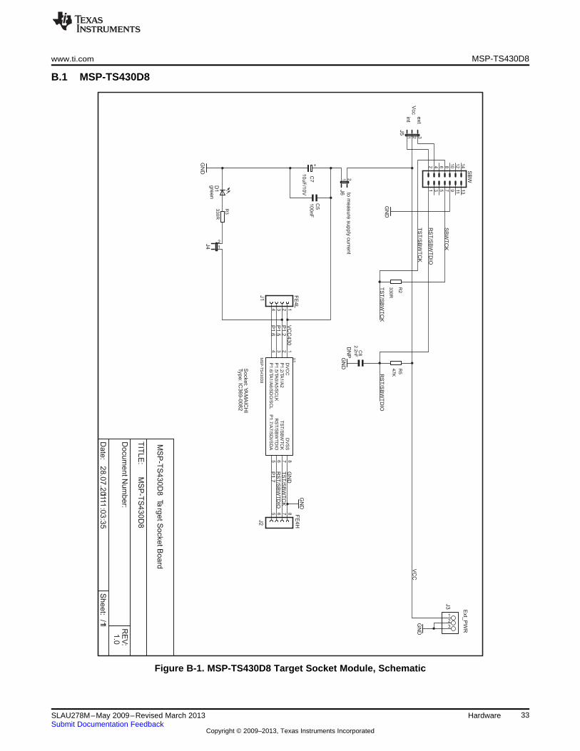
GN
D
10
0n
F
330R
10
uF
/10
V
47K
2.2
nF
GN
D
330R
GN
D
GN
D
gre
en
FE
4L
FE
4H
GN
D
Ext_
PW
R
So
cke
t:YA
MA
ICH
ITyp
e:
IC3
69
-00
82
Vcc
ext
int
tom
ea
su
resu
pp
lycu
rren
tD
NP
1 3 5 7 9 11 13
2 4 6
12
148
10
SB
W
C5R
3
C7
R5
C8
1
2
3
J3
1
2J4
1 2
J6
1 2 3
J5
R2
D1
1234
J1
5 6 7 8
J2
DV
CC
1D
VS
S8
P1.2
/TA1/A
22
P1.5
/TA0/A
5/S
CLK
3
P1.6
/TA1/A
6/S
DO
/SC
L4
TS
T/S
BW
TC
K7
RS
T/S
BW
TD
IO6
P1.7
/A7/S
DI/S
DA
5
U1
MS
P-T
S4
30
D8
GN
D
VC
C
RS
T/S
BW
TD
IO
RS
T/S
BW
TD
IO
RS
T/S
BW
TD
IO
SB
WT
CK
VC
C4
30
TS
T/S
BW
TC
K
TS
T/S
BW
TC
K
TS
T/S
BW
TC
KP
1.5
P1
.6P
1.7
P1
.2
Da
te:
28
.07
.20
1111
:03
:35
Sh
ee
t:1/1
RE
V:
TIT
LE
:
Do
cu
me
nt N
um
be
r:
MS
P-T
S4
30
D8
+
1.0
MS
P-T
S4
30
D8
Targ
et S
ocke
t Bo
ard
www.ti.com MSP-TS430D8
B.1 MSP-TS430D8
Figure B-1. MSP-TS430D8 Target Socket Module, Schematic
33SLAU278M–May 2009–Revised March 2013 HardwareSubmit Documentation Feedback
Copyright © 2009–2013, Texas Instruments Incorporated
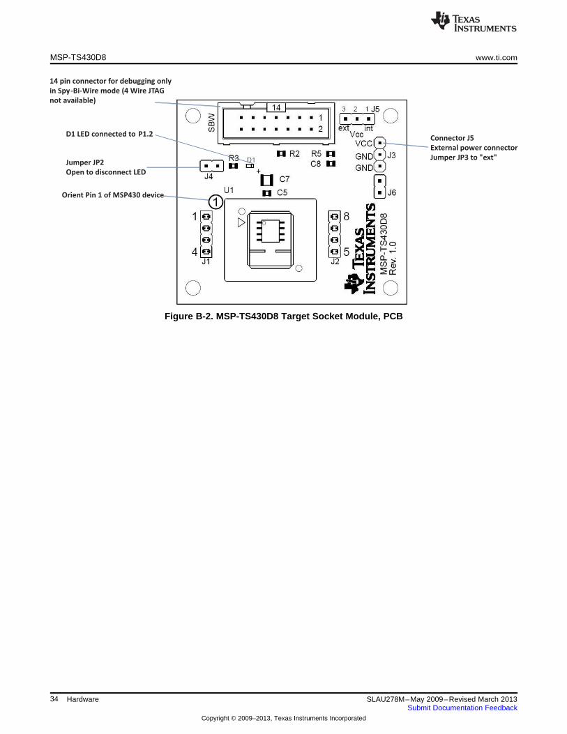
Connector J5
External power connector
Jumper JP3 to "ext"Jumper JP2
Open to disconnect LED
D1 LED connected to P1.2
Orient Pin 1 of MSP430 device
14 pin connector for debugging only
in Spy-Bi-Wire mode (4 Wire JTAG
not available)
MSP-TS430D8 www.ti.com
Figure B-2. MSP-TS430D8 Target Socket Module, PCB
34 Hardware SLAU278M–May 2009–Revised March 2013Submit Documentation Feedback
Copyright © 2009–2013, Texas Instruments Incorporated
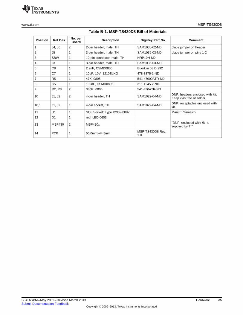
www.ti.com MSP-TS430D8
Table B-1. MSP-TS430D8 Bill of Materials
No. perPosition Ref Des Description DigiKey Part No. CommentBoard
1 J4, J6 2 2-pin header, male, TH SAM1035-02-ND place jumper on header
2 J5 1 3-pin header, male, TH SAM1035-03-ND place jumper on pins 1-2
3 SBW 1 10-pin connector, male, TH HRP10H-ND
4 J3 1 3-pin header, male, TH SAM1035-03-ND
5 C8 1 2.2nF, CSMD0805 Buerklin 53 D 292
6 C7 1 10uF, 10V, 1210ELKO 478-3875-1-ND
7 R5 1 47K, 0805 541-47000ATR-ND
8 C5 1 100nF, CSMD0805 311-1245-2-ND
9 R2, R3 2 330R, 0805 541-330ATR-ND
DNP: headers enclosed with kit.10 J1, J2 2 4-pin header, TH SAM1029-04-ND Keep vias free of solder.
DNP: receptacles enclosed with10,1 J1, J2 1 4-pin socket, TH SAM1029-04-ND kit.
11 U1 1 SO8 Socket: Type IC369-0082 Manuf.: Yamaichi
12 D1 1 red, LED 0603
"DNP: enclosed with kit. Is13 MSP430 2 MSP430x supplied by TI"
MSP-TS430D8 Rev.14 PCB 1 50,0mmx44,5mm 1.0
35SLAU278M–May 2009–Revised March 2013 HardwareSubmit Documentation Feedback
Copyright © 2009–2013, Texas Instruments Incorporated
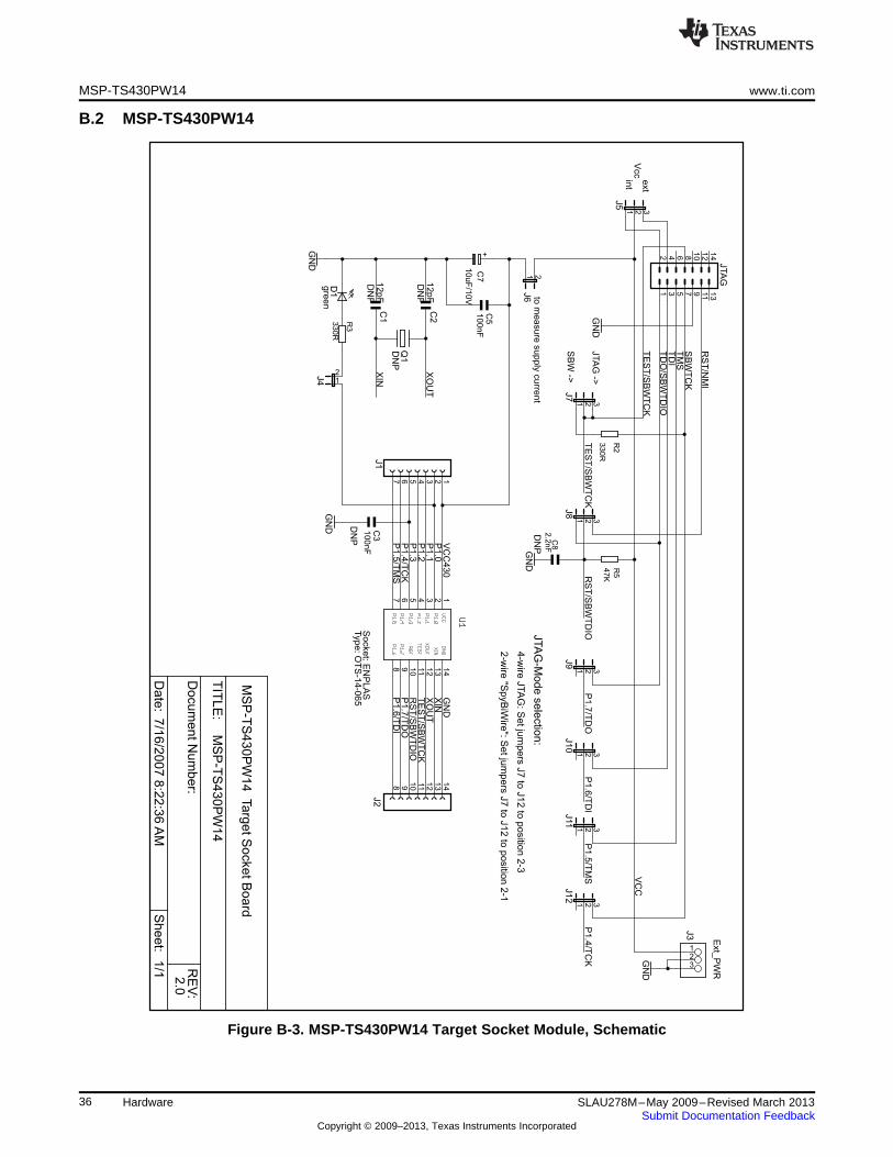
12pF
12pF
GN
D
100nF
330R
10uF
/10V
47K
2.2
nF
GN
D
330R
100nF
GN
D
GN
D
GN
D
gre
en
Ext_
PW
R
Socket: E
NP
LA
SType: O
TS
-14-0
65
Vcc
ext
int
to m
easure
supply
curre
nt
DN
P
DN
P
DN
P
DN
P
DN
P
JTA
G ->
SB
W ->
JTA
G-M
od
e s
ele
ctio
n:
4-w
ire J
TA
G: S
et ju
mp
ers
J7
to J
12
to p
ositio
n 2
-3
2-w
ire "S
pyB
iWire
": Se
t jum
pe
rs J
7 to
J1
2 to
po
sitio
n 2
-1
1 3 5 7 9 11
13
2 4 6
12
148
10
JTA
G
C2
C1
C5R
3
C7
R5
C8
123
J3
Q1
8 910
11
12
13
14
J2
1234567
J1
12J
4
1 2
J6
J5
1 2 3
R2
C3
J7
1 2 3
J8
1 2 3
J9
1 2 3
J10
1 2 3
J11
1 2 3
J12
1 2 3
12345678 9 10
14
13
12
11
D1
P1.0
P1.3
P1.2
P1.1
XO
UT
XO
UT
GN
D
XIN
XIN
VC
C
RS
T/S
BW
TD
IO
RS
T/S
BW
TD
IO
SB
WT
CK
TE
ST
/SB
WT
CK
TE
ST
/SB
WT
CK
TE
ST
/SB
WT
CK
VC
C430
P1.4
/TC
K
P1.4
/TC
K
P1.5
/TM
S
P1.5
/TM
S
P1.6
/TD
I
P1.6
/TD
I
P1.7
/TD
O
P1.7
/TD
O
TD
O/S
BW
TD
IO
RS
T/N
MI
TM
ST
DI
Da
te:
7/1
6/2
00
7 8
:22
:36
AM
Sh
ee
t:1
/1 RE
V:
TIT
LE
:
Do
cu
me
nt N
um
be
r:
MS
P-T
S4
30
PW
14
+
2.0
MS
P-T
S4
30
PW
14
Ta
rge
t So
cke
t Bo
ard
MSP-TS430PW14 www.ti.com
B.2 MSP-TS430PW14
Figure B-3. MSP-TS430PW14 Target Socket Module, Schematic
36 Hardware SLAU278M–May 2009–Revised March 2013Submit Documentation Feedback
Copyright © 2009–2013, Texas Instruments Incorporated
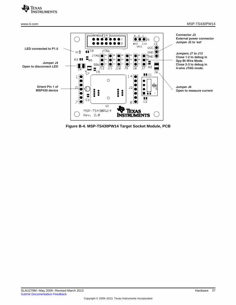
Jumper J4Open to disconnect LED
Orient Pin 1 ofMSP430 device
Jumper J6Open to measure current
Connector J3External power connectorJumper J5 to 'ext'
LED connected to P1.0
Jumpers J7 to J12Close 1-2 to debug inSpy-Bi-Wire Mode.Close 2-3 to debug in4-wire JTAG mode.
www.ti.com MSP-TS430PW14
Figure B-4. MSP-TS430PW14 Target Socket Module, PCB
37SLAU278M–May 2009–Revised March 2013 HardwareSubmit Documentation Feedback
Copyright © 2009–2013, Texas Instruments Incorporated
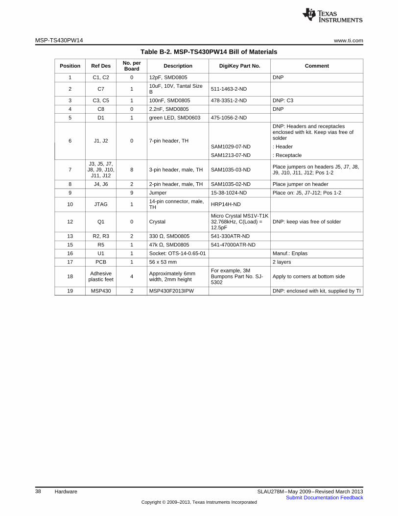
MSP-TS430PW14 www.ti.com
Table B-2. MSP-TS430PW14 Bill of Materials
No. perPosition Ref Des Description DigiKey Part No. CommentBoard
1 C1, C2 0 12pF, SMD0805 DNP
10uF, 10V, Tantal Size2 C7 1 511-1463-2-NDB
3 C3, C5 1 100nF, SMD0805 478-3351-2-ND DNP: C3
4 C8 0 2.2nF, SMD0805 DNP
5 D1 1 green LED, SMD0603 475-1056-2-ND
DNP: Headers and receptaclesenclosed with kit. Keep vias free ofsolder6 J1, J2 0 7-pin header, TH
SAM1029-07-ND : Header
SAM1213-07-ND : Receptacle
J3, J5, J7, Place jumpers on headers J5, J7, J8,7 J8, J9, J10, 8 3-pin header, male, TH SAM1035-03-ND J9, J10, J11, J12; Pos 1-2J11, J12
8 J4, J6 2 2-pin header, male, TH SAM1035-02-ND Place jumper on header
9 9 Jumper 15-38-1024-ND Place on: J5, J7-J12; Pos 1-2
14-pin connector, male,10 JTAG 1 HRP14H-NDTH
Micro Crystal MS1V-T1K12 Q1 0 Crystal 32.768kHz, C(Load) = DNP: keep vias free of solder
12.5pF
13 R2, R3 2 330 Ω, SMD0805 541-330ATR-ND
15 R5 1 47k Ω, SMD0805 541-47000ATR-ND
16 U1 1 Socket: OTS-14-0.65-01 Manuf.: Enplas
17 PCB 1 56 x 53 mm 2 layers
For example, 3MAdhesive Approximately 6mm18 4 Bumpons Part No. SJ- Apply to corners at bottom sideplastic feet width, 2mm height 5302
19 MSP430 2 MSP430F2013IPW DNP: enclosed with kit, supplied by TI
38 Hardware SLAU278M–May 2009–Revised March 2013Submit Documentation Feedback
Copyright © 2009–2013, Texas Instruments Incorporated
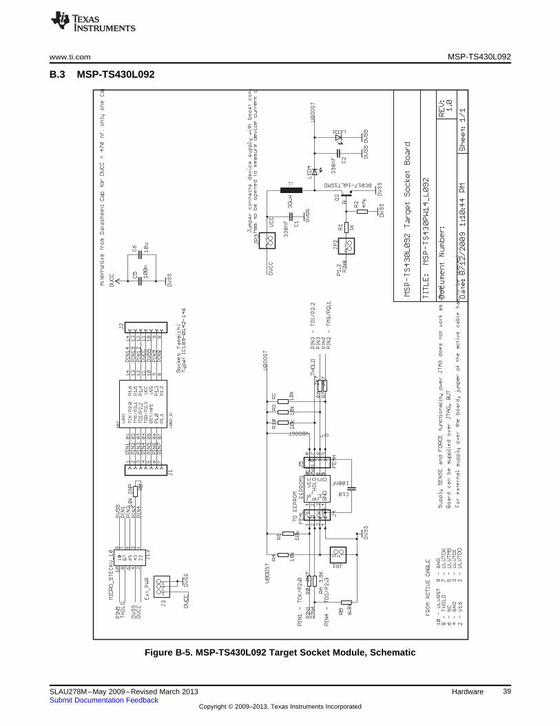
www.ti.com MSP-TS430L092
B.3 MSP-TS430L092
Figure B-5. MSP-TS430L092 Target Socket Module, Schematic
39SLAU278M–May 2009–Revised March 2013 HardwareSubmit Documentation Feedback
Copyright © 2009–2013, Texas Instruments Incorporated
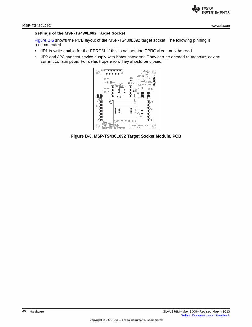
MSP-TS430L092 www.ti.com
Settings of the MSP-TS430L092 Target Socket
Figure B-6 shows the PCB layout of the MSP-TS430L092 target socket. The following pinning isrecommended:
• JP1 is write enable for the EPROM. If this is not set, the EPROM can only be read.
• JP2 and JP3 connect device supply with boost converter. They can be opened to measure devicecurrent consumption. For default operation, they should be closed.
Figure B-6. MSP-TS430L092 Target Socket Module, PCB
40 Hardware SLAU278M–May 2009–Revised March 2013Submit Documentation Feedback
Copyright © 2009–2013, Texas Instruments Incorporated
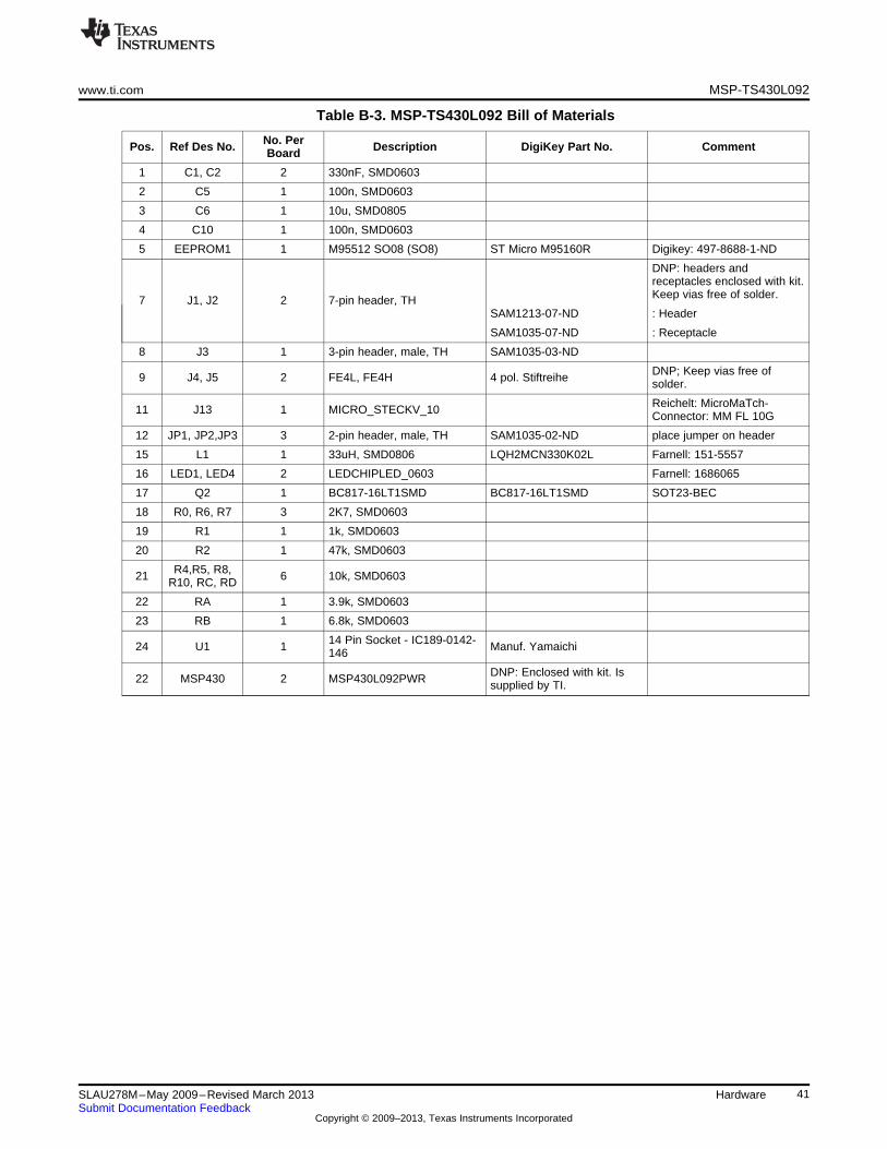
www.ti.com MSP-TS430L092
Table B-3. MSP-TS430L092 Bill of Materials
No. PerPos. Ref Des No. Description DigiKey Part No. CommentBoard
1 C1, C2 2 330nF, SMD0603
2 C5 1 100n, SMD0603
3 C6 1 10u, SMD0805
4 C10 1 100n, SMD0603
5 EEPROM1 1 M95512 SO08 (SO8) ST Micro M95160R Digikey: 497-8688-1-ND
DNP: headers andreceptacles enclosed with kit.Keep vias free of solder.7 J1, J2 2 7-pin header, TH
SAM1213-07-ND : Header
SAM1035-07-ND : Receptacle
8 J3 1 3-pin header, male, TH SAM1035-03-ND
DNP; Keep vias free of9 J4, J5 2 FE4L, FE4H 4 pol. Stiftreihe solder.
Reichelt: MicroMaTch-11 J13 1 MICRO_STECKV_10 Connector: MM FL 10G
12 JP1, JP2,JP3 3 2-pin header, male, TH SAM1035-02-ND place jumper on header
15 L1 1 33uH, SMD0806 LQH2MCN330K02L Farnell: 151-5557
16 LED1, LED4 2 LEDCHIPLED_0603 Farnell: 1686065
17 Q2 1 BC817-16LT1SMD BC817-16LT1SMD SOT23-BEC
18 R0, R6, R7 3 2K7, SMD0603
19 R1 1 1k, SMD0603
20 R2 1 47k, SMD0603
R4,R5, R8,21 6 10k, SMD0603R10, RC, RD
22 RA 1 3.9k, SMD0603
23 RB 1 6.8k, SMD0603
14 Pin Socket - IC189-0142-24 U1 1 Manuf. Yamaichi146
DNP: Enclosed with kit. Is22 MSP430 2 MSP430L092PWR supplied by TI.
41SLAU278M–May 2009–Revised March 2013 HardwareSubmit Documentation Feedback
Copyright © 2009–2013, Texas Instruments Incorporated
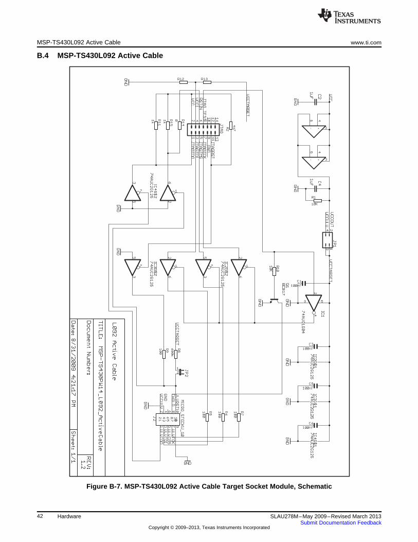
MSP-TS430L092 Active Cable www.ti.com
B.4 MSP-TS430L092 Active Cable
Figure B-7. MSP-TS430L092 Active Cable Target Socket Module, Schematic
42 Hardware SLAU278M–May 2009–Revised March 2013Submit Documentation Feedback
Copyright © 2009–2013, Texas Instruments Incorporated
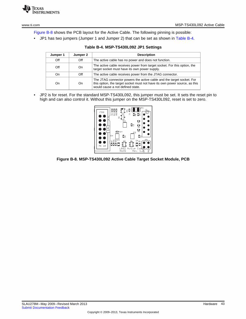
www.ti.com MSP-TS430L092 Active Cable
Figure B-8 shows the PCB layout for the Active Cable. The following pinning is possible:
• JP1 has two jumpers (Jumper 1 and Jumper 2) that can be set as shown in Table B-4.
Table B-4. MSP-TS430L092 JP1 Settings
Jumper 1 Jumper 2 Description
Off Off The active cable has no power and does not function.
The active cable receives power from target socket. For this option, theOff On target socket must have its own power supply.
On Off The active cable receives power from the JTAG connector.
The JTAG connector powers the active cable and the target socket. ForOn On this option, the target socket must not have its own power source, as this
would cause a not defined state.
• JP2 is for reset. For the standard MSP-TS430L092, this jumper must be set. It sets the reset pin tohigh and can also control it. Without this jumper on the MSP-TS430L092, reset is set to zero.
Figure B-8. MSP-TS430L092 Active Cable Target Socket Module, PCB
43SLAU278M–May 2009–Revised March 2013 HardwareSubmit Documentation Feedback
Copyright © 2009–2013, Texas Instruments Incorporated
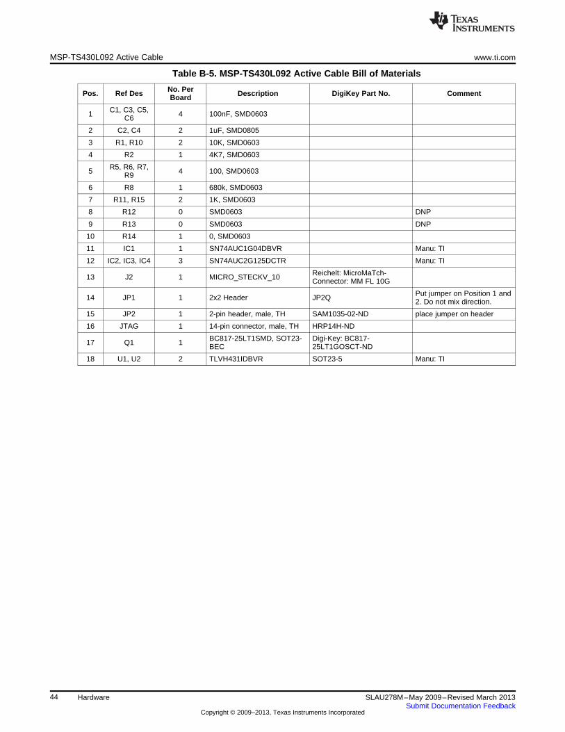
MSP-TS430L092 Active Cable www.ti.com
Table B-5. MSP-TS430L092 Active Cable Bill of Materials
No. PerPos. Ref Des Description DigiKey Part No. CommentBoard
C1, C3, C5,1 4 100nF, SMD0603C6
2 C2, C4 2 1uF, SMD0805
3 R1, R10 2 10K, SMD0603
4 R2 1 4K7, SMD0603
R5, R6, R7,5 4 100, SMD0603R9
6 R8 1 680k, SMD0603
7 R11, R15 2 1K, SMD0603
8 R12 0 SMD0603 DNP
9 R13 0 SMD0603 DNP
10 R14 1 0, SMD0603
11 IC1 1 SN74AUC1G04DBVR Manu: TI
12 IC2, IC3, IC4 3 SN74AUC2G125DCTR Manu: TI
Reichelt: MicroMaTch-13 J2 1 MICRO_STECKV_10 Connector: MM FL 10G
Put jumper on Position 1 and14 JP1 1 2x2 Header JP2Q 2. Do not mix direction.
15 JP2 1 2-pin header, male, TH SAM1035-02-ND place jumper on header
16 JTAG 1 14-pin connector, male, TH HRP14H-ND
BC817-25LT1SMD, SOT23- Digi-Key: BC817-17 Q1 1 BEC 25LT1GOSCT-ND
18 U1, U2 2 TLVH431IDBVR SOT23-5 Manu: TI
44 Hardware SLAU278M–May 2009–Revised March 2013Submit Documentation Feedback
Copyright © 2009–2013, Texas Instruments Incorporated
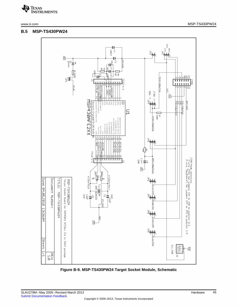
www.ti.com MSP-TS430PW24
B.5 MSP-TS430PW24
Figure B-9. MSP-TS430PW24 Target Socket Module, Schematic
45SLAU278M–May 2009–Revised March 2013 HardwareSubmit Documentation Feedback
Copyright © 2009–2013, Texas Instruments Incorporated
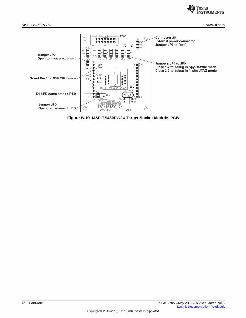
Jumper JP2Open to measure current
Orient Pin 1 of MSP430 device
D1 LED connected to P1.0
Jumper JP3Open to disconnect LED
Connector J5External power connectorJumper JP1 to "ext"
Jumpers JP4 to JP9Close 1-2 to debug in Spy-Bi-Wire modeClose 2-3 to debug in 4-wire JTAG mode
MSP-TS430PW24 www.ti.com
Figure B-10. MSP-TS430PW24 Target Socket Module, PCB
46 Hardware SLAU278M–May 2009–Revised March 2013Submit Documentation Feedback
Copyright © 2009–2013, Texas Instruments Incorporated
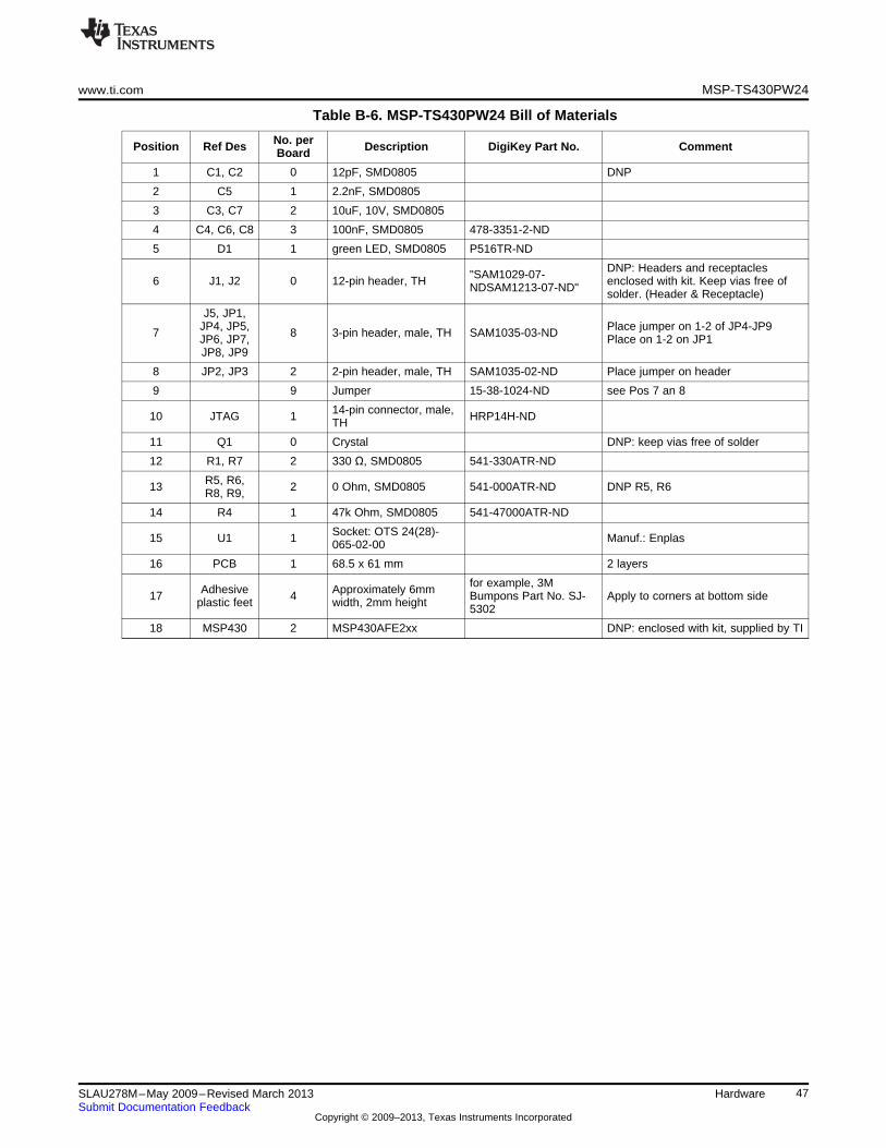
www.ti.com MSP-TS430PW24
Table B-6. MSP-TS430PW24 Bill of Materials
No. perPosition Ref Des Description DigiKey Part No. CommentBoard
1 C1, C2 0 12pF, SMD0805 DNP
2 C5 1 2.2nF, SMD0805
3 C3, C7 2 10uF, 10V, SMD0805
4 C4, C6, C8 3 100nF, SMD0805 478-3351-2-ND
5 D1 1 green LED, SMD0805 P516TR-ND
DNP: Headers and receptacles"SAM1029-07-6 J1, J2 0 12-pin header, TH enclosed with kit. Keep vias free ofNDSAM1213-07-ND" solder. (Header & Receptacle)
J5, JP1,JP4, JP5, Place jumper on 1-2 of JP4-JP97 8 3-pin header, male, TH SAM1035-03-NDJP6, JP7, Place on 1-2 on JP1JP8, JP9
8 JP2, JP3 2 2-pin header, male, TH SAM1035-02-ND Place jumper on header
9 9 Jumper 15-38-1024-ND see Pos 7 an 8
14-pin connector, male,10 JTAG 1 HRP14H-NDTH
11 Q1 0 Crystal DNP: keep vias free of solder
12 R1, R7 2 330 Ω, SMD0805 541-330ATR-ND
R5, R6,13 2 0 Ohm, SMD0805 541-000ATR-ND DNP R5, R6R8, R9,
14 R4 1 47k Ohm, SMD0805 541-47000ATR-ND
Socket: OTS 24(28)-15 U1 1 Manuf.: Enplas065-02-00
16 PCB 1 68.5 x 61 mm 2 layers
for example, 3MAdhesive Approximately 6mm17 4 Bumpons Part No. SJ- Apply to corners at bottom sideplastic feet width, 2mm height 5302
18 MSP430 2 MSP430AFE2xx DNP: enclosed with kit, supplied by TI
47SLAU278M–May 2009–Revised March 2013 HardwareSubmit Documentation Feedback
Copyright © 2009–2013, Texas Instruments Incorporated
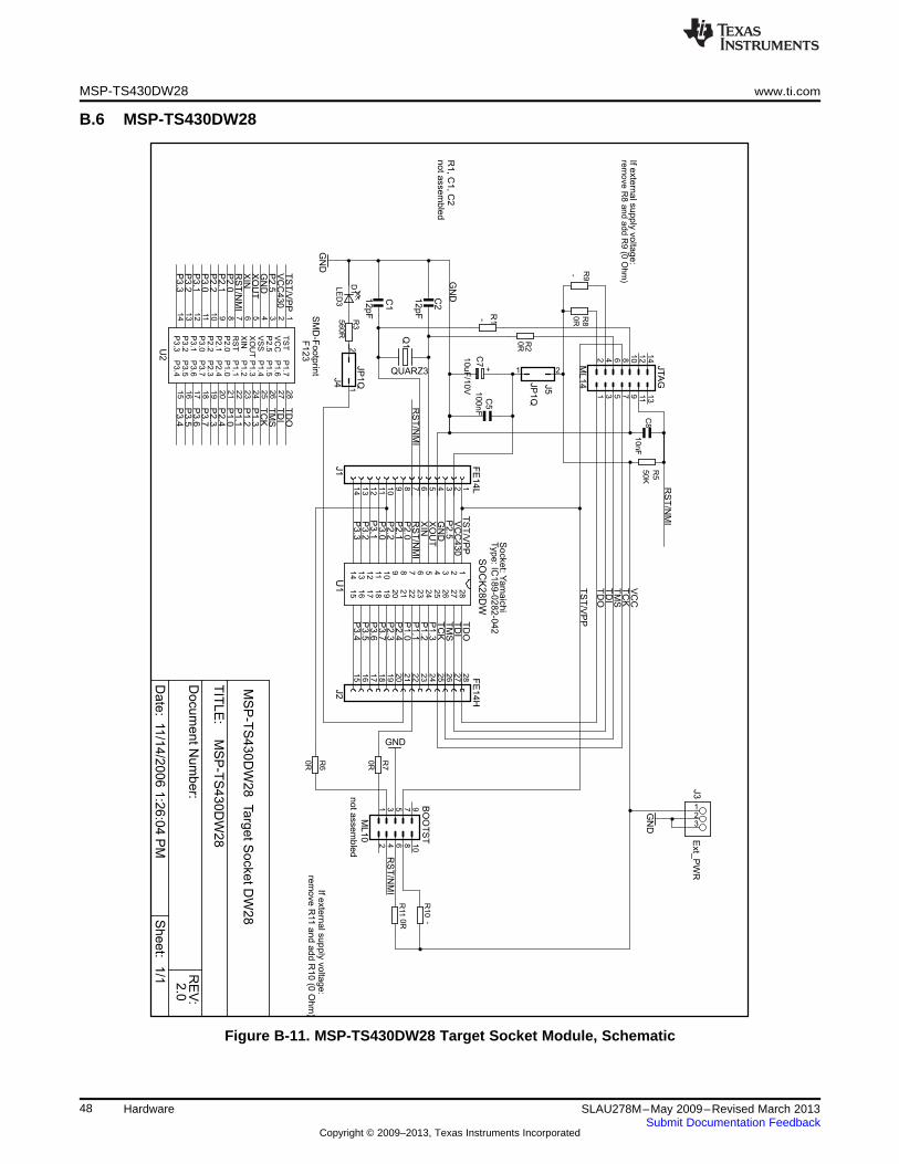
ML
14
LE
D3
12
pF
12
pF
GN
D
GND
10
0n
F
56
0R
ML
10
JP
1Q
JP
1Q
10
uF
/10
V
50
K1
0n
F
0R
0R
0R
-
-0R
-
U1
SO
CK
28
DW
F1
23
FE
14
HF
E1
4L
0R
GN
D
rem
ove
R8
an
d a
dd
R9
(0 O
hm
)
If exte
rna
l su
pp
ly v
olta
ge
:re
mo
ve
R11
an
d a
dd
R1
0 (0
Oh
m)
SM
D-F
oo
tprin
t
So
cke
t:Y
am
aic
hi
2.0
MS
P-T
S4
30
DW
28
Ta
rge
t So
cke
t DW
28
Typ
e: IC
18
9-0
28
2-0
42
If exte
rna
l su
pp
ly v
olta
ge
:
R1
, C1
, C2
no
t asse
mb
led
no
t asse
mb
led
1 3 5 7 9 11
13
2 4 6
12
148
10
JTA
G
D1
C2
C1
C5
R3
BO
OT
ST
12
34
56
78
91
0
1 2
J5
J4
12
C7
R5
C8
R6
R7
R8
R9
R1
0
R11
R1
12345678910
11
12
13
14
15
16
17
18
19
20
21
22
23
24
25
26
27
28
TS
T1
VC
C2
P2
.53
VS
S4
XO
UT
5
XIN
6
RS
T7
P2
.08
P2
.19
P2
.21
0P
2.3
19
P2
.42
0P
1.0
21
P1
.12
2P
1.2
23
P1
.32
4P
1.4
25
P1
.52
6P
1.6
27
P1
.72
8
P3
.011
P3
.11
2
P3
.21
3
P3
.31
4P
3.4
15
P3
.51
6P
3.6
17
P3
.71
8
U2
15
16
17
18
19
20
21
22
23
24
25
26
27
28
J2
J1
12345678910
11
12
13
14
R2
123
J3
Q1
QUARZ3
P1
.0
P1
.0
P1
.3
P1
.3
P1
.2
P1
.2
P1
.1
P1
.1R
ST
/NM
I
RS
T/N
MI
RS
T/N
MIRS
T/N
MI
RS
T/N
MI
TC
K
TC
K
TC
K
TM
S
TM
S
TM
S
TD
I
TD
I
TD
I
TD
O
TD
O
TD
O
XO
UT
XO
UT
VC
C
GN
D
GN
D
GN
D
P2
.3
P2
.3
P2
.4
P2
.4
XIN
XIN
P2
.5
P2
.5
P2
.2
P2
.2P
2.1
P2
.1
P2
.0
P2
.0
TS
T/V
PP
TS
T/V
PP
TS
T/V
PP
P3
.0
P3
.0
P3
.1
P3
.1
P3
.2
P3
.2
P3
.3
P3
.3
P3
.7
P3
.7
P3
.6
P3
.6
P3
.5
P3
.5
P3
.4
P3
.4
VC
C4
30
Ext_
PW
R
Da
te:
11
/14
/20
06
1:2
6:0
4 P
MS
he
et:
1/1 R
EV
:
TIT
LE
:
Do
cu
me
nt N
um
be
r:
MS
P-T
S4
30
DW
28
+
VC
C4
30
MSP-TS430DW28 www.ti.com
B.6 MSP-TS430DW28
Figure B-11. MSP-TS430DW28 Target Socket Module, Schematic
48 Hardware SLAU278M–May 2009–Revised March 2013Submit Documentation Feedback
Copyright © 2009–2013, Texas Instruments Incorporated
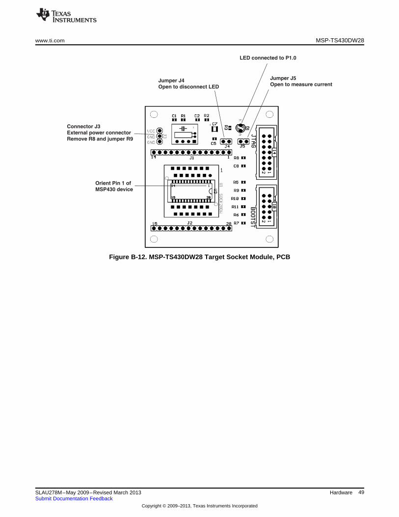
Jumper J4
Open to disconnect LED
Orient Pin 1 of
MSP430 device
Jumper J5
Open to measure current
Connector J3
External power connector
Remove R8 and jumper R9
LED connected to P1.0
www.ti.com MSP-TS430DW28
Figure B-12. MSP-TS430DW28 Target Socket Module, PCB
49SLAU278M–May 2009–Revised March 2013 HardwareSubmit Documentation Feedback
Copyright © 2009–2013, Texas Instruments Incorporated
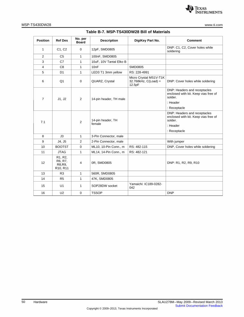
MSP-TS430DW28 www.ti.com
Table B-7. MSP-TS430DW28 Bill of Materials
No. perPosition Ref Des Description DigiKey Part No. CommentBoard
DNP: C1, C2, Cover holes while1 C1, C2 0 12pF, SMD0805 soldering
2 C5 1 100nF, SMD0805
3 C7 1 10uF, 10V Tantal Elko B
4 C8 1 10nF SMD0805
5 D1 1 LED3 T1 3mm yellow RS: 228-4991
Micro Crystal MS1V-T1K6 Q1 0 QUARZ, Crystal 32.768kHz, C(Load) = DNP: Cover holes while soldering
12.5pF
DNP: Headers and receptaclesenclosed with kit. Keep vias free ofsolder.7 J1, J2 2 14-pin header, TH male: Header
: Receptacle
DNP: Headers and receptaclesenclosed with kit. Keep vias free of
14-pin header, TH solder.7.1 2 female : Header
: Receptacle
8 J3 1 3-Pin Connector, male
9 J4, J5 2 2-Pin Connector, male With jumper
10 BOOTST 0 ML10, 10-Pin Conn., m RS: 482-115 DNP, Cover holes while soldering
11 JTAG 1 ML14, 14-Pin Conn., m RS: 482-121
R1, R2,R6, R7,12 4 0R, SMD0805 DNP: R1, R2, R9, R10R8,R9,
R10, R11
13 R3 1 560R, SMD0805
14 R5 1 47K, SMD0805
Yamaichi: IC189-0282-15 U1 1 SOP28DW socket 042
16 U2 0 TSSOP DNP
50 Hardware SLAU278M–May 2009–Revised March 2013Submit Documentation Feedback
Copyright © 2009–2013, Texas Instruments Incorporated
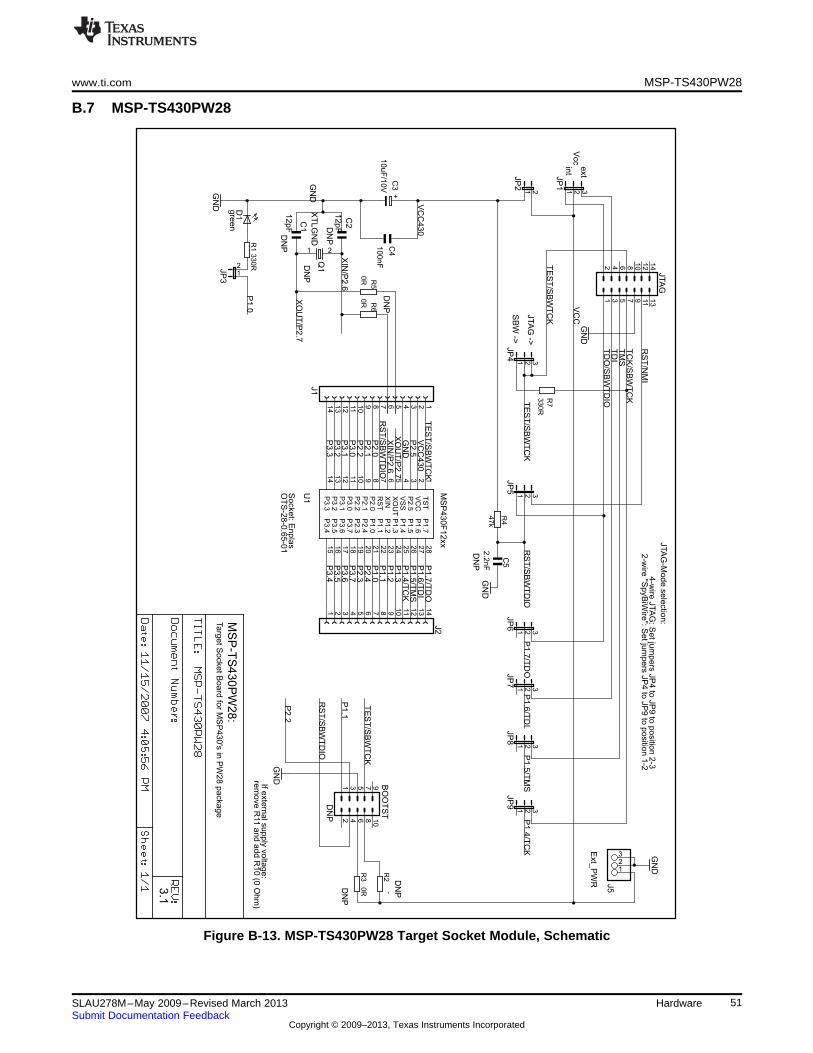
12pF
12pF
GN
D
GN
D
100nF
33
0R
10uF
/10V
-
0R
GN
D
GN
D
gre
en
2.2
nF
47
kG
ND
0R
0R
33
0R
MS
P430F
12xx
If exte
rnal s
upply
volta
ge:
rem
ove R
11 a
nd a
dd R
10 (0
Ohm
)
3.1
MS
P-T
S4
30
PW
28
:
OT
S-2
8-0
.65-0
1S
ocket: E
npla
s
Vcc
int
ext
Targ
et S
ocket B
oard
for M
SP
430
's in
PW
28 p
ackage
DN
P
DN
P
DN
P
DN
P
DN
P
DN
P
DN
P
JTA
G ->
SB
W ->
JTA
G-M
ode s
ele
ctio
n:
4-w
ire J
TA
G: S
et ju
mpers
JP
4 to
JP
9 to
positio
n 2
-32-w
ire "S
pyB
iWire
": Set ju
mpers
JP
4 to
JP
9 to
positio
n 1
-2
DN
P
1 3 5 7 9 11
13
2 4 6
12
148
10
JTA
G
C2C1
C4
R1
12
34
56
78
91
0
BO
OT
ST
C3
R2
R3
123
J5
JP
1
1 2 3
JP
2
1 212J
P3
D1
C5
R4
JP
4
1 2 3
JP
5
1 2 3
JP
6
1 2 3
JP
7
1 2 3
JP
8
1 2 3
JP
9
1 2 3
R5
R6
21
Q1
R7
J1
12345678910
11
12
13
14
J2
1 2 3 4 5 6 7 8 91
011
12
13
14
U1 TS
T1
VC
C2
P2
.53
VS
S4
XO
UT
5
XIN
6
RS
T7
P2
.08
P2
.19
P2
.21
0P
2.3
19
P2
.42
0P
1.0
21
P1
.12
2P
1.2
23
P1
.32
4P
1.4
25
P1
.52
6P
1.6
27
P1
.72
8
P3
.011
P3
.11
2
P3
.21
3
P3
.31
4P
3.4
15
P3
.51
6P
3.6
17
P3
.71
8
P1.0
P1.0
RS
T/N
MI
TM
ST
DI
VC
C
GN
D
GN
D
VC
C430
VC
C430
P2.0
P1.1
P1.1
P3.3
P3.2
P3.1
P3.0
P2.2
P2.2
XIN
/P2.6
XIN
/P2.6
XO
UT
/P2.7
XO
UT
/P2.7
P2.1
RS
T/S
BW
TD
IO
RS
T/S
BW
TD
IO
RS
T/S
BW
TD
IO
P3.4
P3.5
P3.6
P3.7
P2.3
P2.4
P1.2
P1.3
P1.4
/TC
K
P1.4
/TC
K
P1.5
/TM
S
P1.5
/TM
S
P1.6
/TD
I
P1.6
/TD
I
P1.7
/TD
O
P1.7
/TD
O
TE
ST
/SB
WT
CK
TE
ST
/SB
WT
CK
TE
ST
/SB
WT
CK
TE
ST
/SB
WT
CK
P2.5
TC
K/S
BW
TC
K
TD
O/S
BW
TD
IO
XT
LG
ND
Ext_
PW
R
+
www.ti.com MSP-TS430PW28
B.7 MSP-TS430PW28
Figure B-13. MSP-TS430PW28 Target Socket Module, Schematic
51SLAU278M–May 2009–Revised March 2013 HardwareSubmit Documentation Feedback
Copyright © 2009–2013, Texas Instruments Incorporated
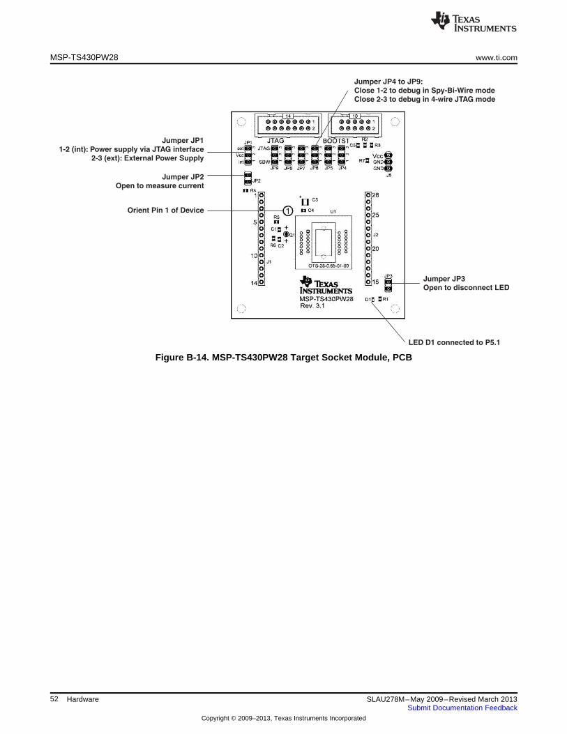
Jumper JP2Open to measure current
Jumper JP3Open to disconnect LED
LED D1 connected to P5.1
Jumper JP11-2 (int): Power supply via JTAG interface
2-3 (ext): External Power Supply
Jumper JP4 to JP9:Close 1-2 to debug in Spy-Bi-Wire modeClose 2-3 to debug in 4-wire JTAG mode
Orient Pin 1 of Device
MSP-TS430PW28 www.ti.com
Figure B-14. MSP-TS430PW28 Target Socket Module, PCB
52 Hardware SLAU278M–May 2009–Revised March 2013Submit Documentation Feedback
Copyright © 2009–2013, Texas Instruments Incorporated
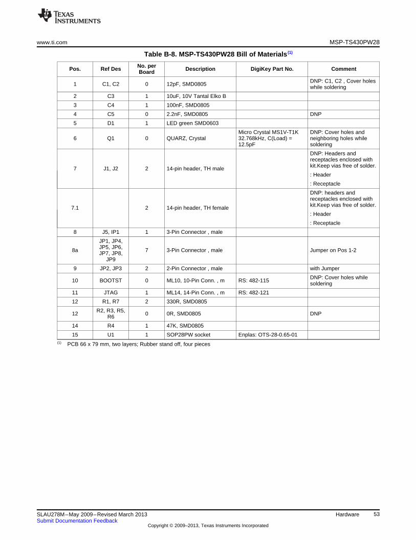
www.ti.com MSP-TS430PW28
Table B-8. MSP-TS430PW28 Bill of Materials (1)
No. perPos. Ref Des Description DigiKey Part No. CommentBoard
DNP: C1, C2 , Cover holes1 C1, C2 0 12pF, SMD0805 while soldering
2 C3 1 10uF, 10V Tantal Elko B
3 C4 1 100nF, SMD0805
4 C5 0 2.2nF, SMD0805 DNP
5 D1 1 LED green SMD0603
Micro Crystal MS1V-T1K DNP: Cover holes and6 Q1 0 QUARZ, Crystal 32.768kHz, C(Load) = neighboring holes while
12.5pF soldering
DNP: Headers andreceptacles enclosed withkit.Keep vias free of solder.7 J1, J2 2 14-pin header, TH male: Header
: Receptacle
DNP: headers andreceptacles enclosed withkit.Keep vias free of solder.7.1 2 14-pin header, TH female: Header
: Receptacle
8 J5, IP1 1 3-Pin Connector , male
JP1, JP4,JP5, JP6,8a 7 3-Pin Connector , male Jumper on Pos 1-2JP7, JP8,
JP9
9 JP2, JP3 2 2-Pin Connector , male with Jumper
DNP: Cover holes while10 BOOTST 0 ML10, 10-Pin Conn. , m RS: 482-115 soldering
11 JTAG 1 ML14, 14-Pin Conn. , m RS: 482-121
12 R1, R7 2 330R, SMD0805
R2, R3, R5,12 0 0R, SMD0805 DNPR6
14 R4 1 47K, SMD0805
15 U1 1 SOP28PW socket Enplas: OTS-28-0.65-01(1) PCB 66 x 79 mm, two layers; Rubber stand off, four pieces
53SLAU278M–May 2009–Revised March 2013 HardwareSubmit Documentation Feedback
Copyright © 2009–2013, Texas Instruments Incorporated
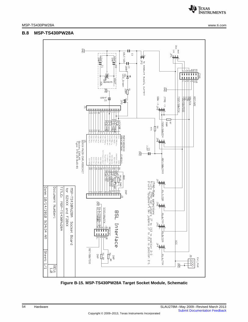
MSP-TS430PW28A www.ti.com
B.8 MSP-TS430PW28A
Figure B-15. MSP-TS430PW28A Target Socket Module, Schematic
54 Hardware SLAU278M–May 2009–Revised March 2013Submit Documentation Feedback
Copyright © 2009–2013, Texas Instruments Incorporated
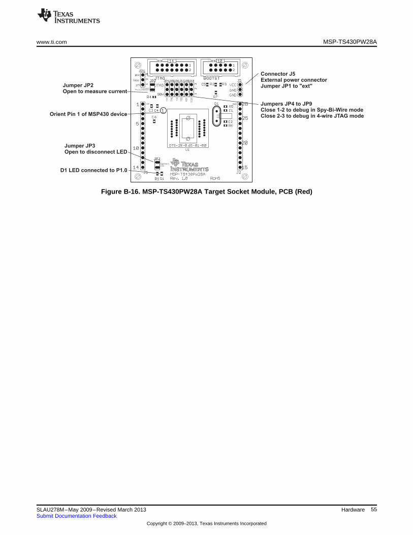
Jumper JP2Open to measure current
Orient Pin 1 of MSP430 device
Jumper JP3Open to disconnect LED
D1 LED connected to P1.0
Connector J5External power connectorJumper JP1 to "ext"
Jumpers JP4 to JP9Close 1-2 to debug in Spy-Bi-Wire modeClose 2-3 to debug in 4-wire JTAG mode
www.ti.com MSP-TS430PW28A
Figure B-16. MSP-TS430PW28A Target Socket Module, PCB (Red)
55SLAU278M–May 2009–Revised March 2013 HardwareSubmit Documentation Feedback
Copyright © 2009–2013, Texas Instruments Incorporated
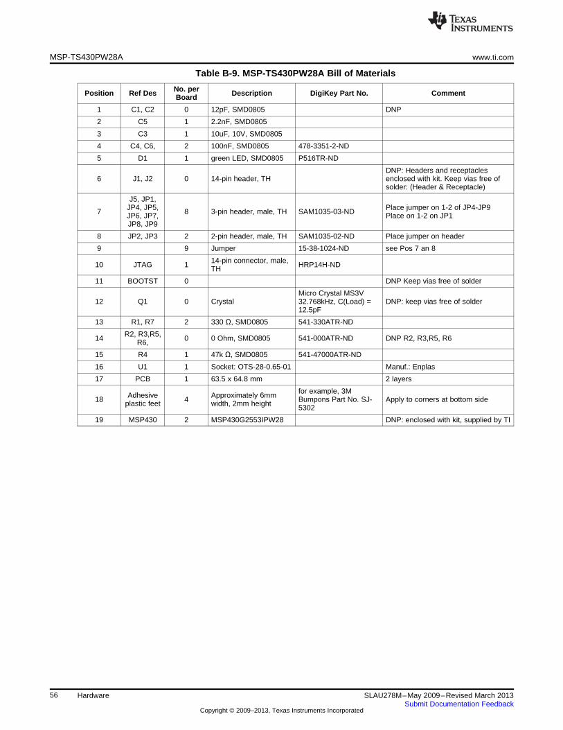
MSP-TS430PW28A www.ti.com
Table B-9. MSP-TS430PW28A Bill of Materials
No. perPosition Ref Des Description DigiKey Part No. CommentBoard
1 C1, C2 0 12pF, SMD0805 DNP
2 C5 1 2.2nF, SMD0805
3 C3 1 10uF, 10V, SMD0805
4 C4, C6, 2 100nF, SMD0805 478-3351-2-ND
5 D1 1 green LED, SMD0805 P516TR-ND
DNP: Headers and receptacles6 J1, J2 0 14-pin header, TH enclosed with kit. Keep vias free of
solder: (Header & Receptacle)
J5, JP1,JP4, JP5, Place jumper on 1-2 of JP4-JP97 8 3-pin header, male, TH SAM1035-03-NDJP6, JP7, Place on 1-2 on JP1JP8, JP9
8 JP2, JP3 2 2-pin header, male, TH SAM1035-02-ND Place jumper on header
9 9 Jumper 15-38-1024-ND see Pos 7 an 8
14-pin connector, male,10 JTAG 1 HRP14H-NDTH
11 BOOTST 0 DNP Keep vias free of solder
Micro Crystal MS3V12 Q1 0 Crystal 32.768kHz, C(Load) = DNP: keep vias free of solder
12.5pF
13 R1, R7 2 330 Ω, SMD0805 541-330ATR-ND
R2, R3,R5,14 0 0 Ohm, SMD0805 541-000ATR-ND DNP R2, R3,R5, R6R6,
15 R4 1 47k Ω, SMD0805 541-47000ATR-ND
16 U1 1 Socket: OTS-28-0.65-01 Manuf.: Enplas
17 PCB 1 63.5 x 64.8 mm 2 layers
for example, 3MAdhesive Approximately 6mm18 4 Bumpons Part No. SJ- Apply to corners at bottom sideplastic feet width, 2mm height 5302
19 MSP430 2 MSP430G2553IPW28 DNP: enclosed with kit, supplied by TI
56 Hardware SLAU278M–May 2009–Revised March 2013Submit Documentation Feedback
Copyright © 2009–2013, Texas Instruments Incorporated
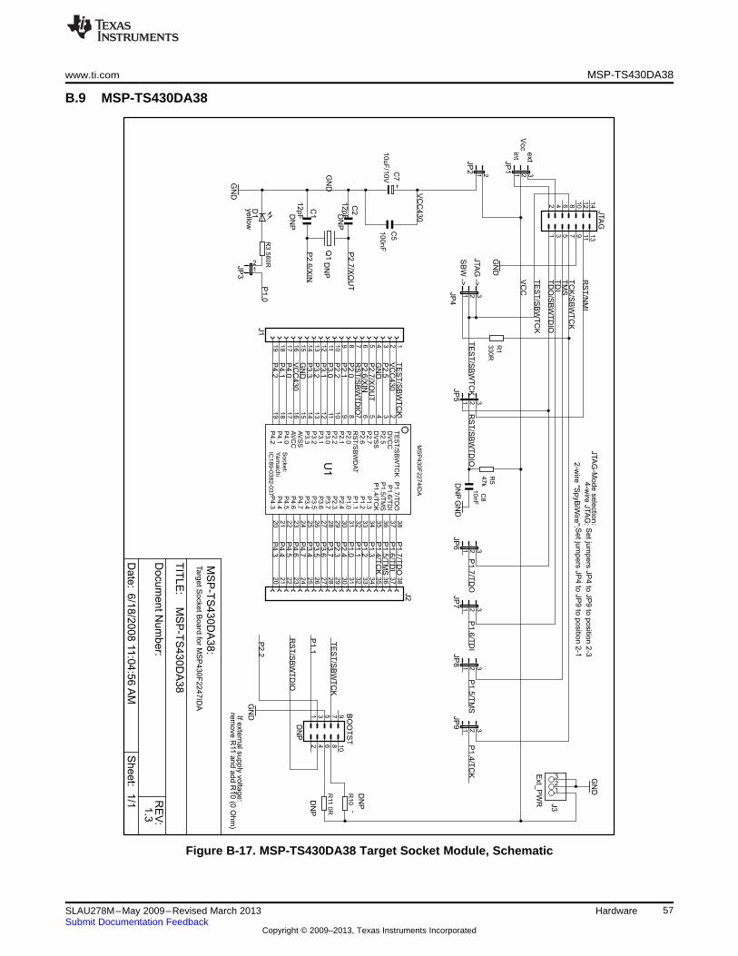
12
pF
12
pF
GN
D
GN
D
10
0n
F
560R
10
uF
/10
V
47k
10nF
-
0R
GN
D
MS
P4
30
F2
27
4ID
A
GN
D330R
GN
D
ye
llow
If exte
rna
l su
pp
ly v
olta
ge
:re
mo
ve
R11
an
d a
dd
R1
0 (0
Oh
m)
IC1
89
-03
82
-03
7
So
cke
t:
4-w
ire J
TA
G:
2-w
ire "S
pyB
iWire
":
JTA
G-M
od
e s
ele
ctio
n:
Se
t jum
pe
rs J
P4
to J
P9
to p
ositio
n 2
-3
Se
t jum
pe
rs J
P4
to J
P9
to p
ositio
n 2
-1
JTA
G ->
SB
W ->
Ya
ma
ich
i
DN
P
DN
P
DN
PD
NP
DN
P
DN
P
DN
P
1 3 5 7 9 11
13
2 4 6
12
148
10
JTA
G
C2C1
C5
R3
12
34
56
78
910
BO
OT
ST
C7
R5
C8
R10
R11
123
J3
Q1
TE
ST
/SB
WT
CK
1
P3.5
26
P3.6
27
P1.4
/TC
K35
RS
T/S
BW
DA
T7
DV
CC
2
DV
SS
4
P4.7
24
P3.7
28
AV
SS
15
AV
CC
16
P3.0
11
P3.1
12
P3.2
13
P3.3
14
P4.0
17
P4.1
18
P4.2
19
P3.4
25
P2.5
3
P2.4
30
P2.3
29
P2.2
10
P2.1
9P
2.0
8
P1.5
/TM
S36
P1.6
/TD
I37
P1.7
/TD
O38
P2.7
5
P2.6
6
P4.6
23
P4.5
22
P4.4
21
P4.3
20
P1.0
31
P1.1
32
P1.2
33
P1.3
34
U1
JP
1
1 2 3
JP
2
1 2
12J
P3
1 2 3JP
4JP
5
1 2 3
JP
6
1 2 3
JP
7
1 2 3
JP
8
1 2 3
R1
JP
9
1 2 3
2345678910
11
12
13
14
15
16
17
18
19
1
J1
21
22
23
24
25
26
27
28
29
30
31
32
33
34
35
36
37
38
20
J2
D1
P1
.0
P1
.0
RS
T/N
MI
TM
ST
DI
VC
C
GN
D
GN
D
GN
DV
CC
43
0
VC
C4
30
VC
C4
30
TC
K/S
BW
TC
K
TD
O/S
BW
TD
IO
TE
ST
/SB
WT
CK
TE
ST
/SB
WT
CK
TE
ST
/SB
WT
CK
TE
ST
/SB
WT
CK
P2
.5
P2
.0P
2.1
P3
.0P
3.1
P3
.2P
3.3
P4
.0P
4.1
P4
.2
P1
.7/T
DO
P1
.7/T
DO
P1
.6/T
DI
P1
.6/T
DI
P1
.5/T
MS
P1
.5/T
MS
P1
.4/T
CK
P1
.4/T
CK
P1
.3P
1.2
P1
.1
P1
.1
P2
.4P
2.3
P3
.7P
3.6
P3
.5P
3.4
P4
.7P
4.6
P4
.5P
4.4
P4
.3
P2
.7/X
OU
T
P2
.7/X
OU
T
P2
.6/X
IN
P2
.6/X
IN
RS
T/S
BW
TD
IO
RS
T/S
BW
TD
IO
RS
T/S
BW
TD
IO
P2
.2
P2
.2
Ext_
PW
R
Date
:6/1
8/2
008 1
1:0
4:5
6A
MS
heet:
1/1 R
EV
:
TIT
LE
:
Docum
ent N
um
ber:
MS
P-T
S430D
A38
+
1.3
MS
P-T
S430D
A38:
Vcc
int
ext
Ta
rge
t So
cke
t Bo
ard
for M
SP
43
0F
22
47
IDA
www.ti.com MSP-TS430DA38
B.9 MSP-TS430DA38
Figure B-17. MSP-TS430DA38 Target Socket Module, Schematic
57SLAU278M–May 2009–Revised March 2013 HardwareSubmit Documentation Feedback
Copyright © 2009–2013, Texas Instruments Incorporated
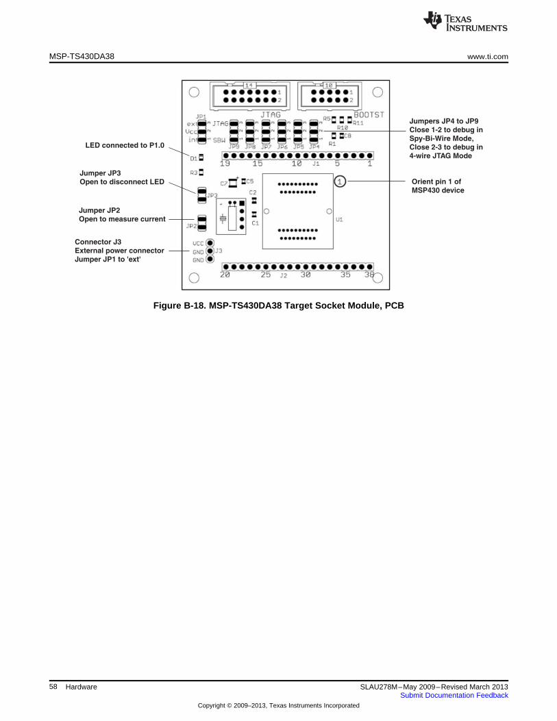
Orient pin 1 ofMSP430 device
LED connected to P1.0
Connector J3External power connectorJumper JP1 to 'ext'
Jumper JP3Open to disconnect LED
Jumper JP2Open to measure current
Jumpers JP4 to JP9Close 1-2 to debug inSpy-Bi-Wire Mode,Close 2-3 to debug in4-wire JTAG Mode
MSP-TS430DA38 www.ti.com
Figure B-18. MSP-TS430DA38 Target Socket Module, PCB
58 Hardware SLAU278M–May 2009–Revised March 2013Submit Documentation Feedback
Copyright © 2009–2013, Texas Instruments Incorporated
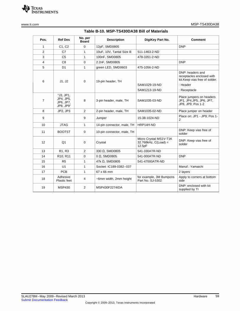
www.ti.com MSP-TS430DA38
Table B-10. MSP-TS430DA38 Bill of Materials
No. perPos. Ref Des Description DigiKey Part No. CommentBoard
1 C1, C2 0 12pF, SMD0805 DNP
2 C7 1 10uF, 10V, Tantal Size B 511-1463-2-ND
3 C5 1 100nF, SMD0805 478-3351-2-ND
4 C8 0 2.2nF, SMD0805 DNP
5 D1 1 green LED, SMD0603 475-1056-2-ND
DNP: headers andreceptacles enclosed withkit.Keep vias free of solder.6 J1, J2 0 19-pin header, TH
SAM1029-19-ND : Header
SAM1213-19-ND : Receptacle
"J3, JP1, Place jumpers on headersJP4, JP5,7 8 3-pin header, male, TH SAM1035-03-ND JP1, JP4,JP5, JP6, JP7,JP6, JP7, JP8, JP9; Pos 1-2JP8, JP9"
8 JP2, JP3 2 2-pin header, male, TH SAM1035-02-ND Place jumper on header
Place on: JP1 - JP9; Pos 1-9 9 Jumper 15-38-1024-ND 2
10 JTAG 1 14-pin connector, male, TH HRP14H-ND
DNP: Keep vias free of11 BOOTST 0 10-pin connector, male, TH solder
Micro Crystal MS1V-T1K DNP: Keep vias free of12 Q1 0 Crystal 32.768kHz, C(Load) = solder12.5pF
13 R1, R3 2 330 Ω, SMD0805 541-330ATR-ND
14 R10, R11 0 0 Ω, SMD0805 541-000ATR-ND DNP
15 R5 1 47k Ω, SMD0805 541-47000ATR-ND
16 U1 1 Socket: IC189-0382--037 Manuf.: Yamaichi
17 PCB 1 67 x 66 mm 2 layers
Adhesive for example, 3M Bumpons Apply to corners at bottom18 4 ~6mm width, 2mm heightPlastic feet Part No. SJ-5302 side
DNP: enclosed with kit19 MSP430 2 MSP430F2274IDA supplied by TI
59SLAU278M–May 2009–Revised March 2013 HardwareSubmit Documentation Feedback
Copyright © 2009–2013, Texas Instruments Incorporated
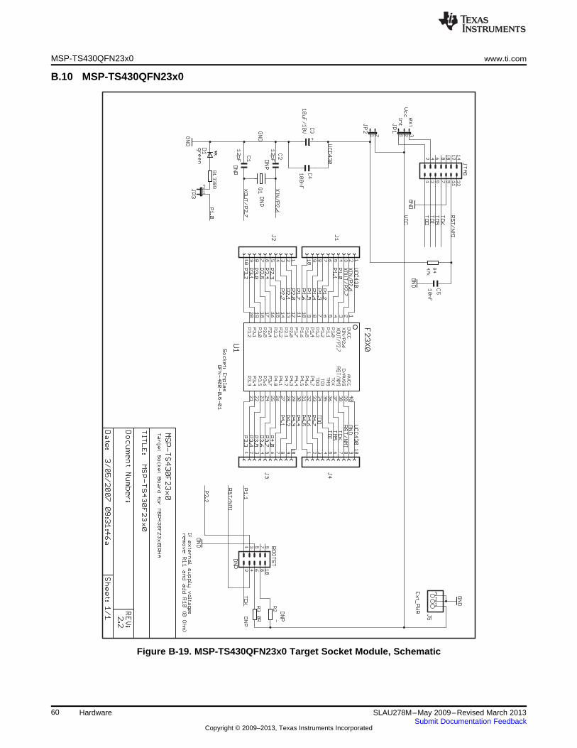
MSP-TS430QFN23x0 www.ti.com
B.10 MSP-TS430QFN23x0
Figure B-19. MSP-TS430QFN23x0 Target Socket Module, Schematic
60 Hardware SLAU278M–May 2009–Revised March 2013Submit Documentation Feedback
Copyright © 2009–2013, Texas Instruments Incorporated
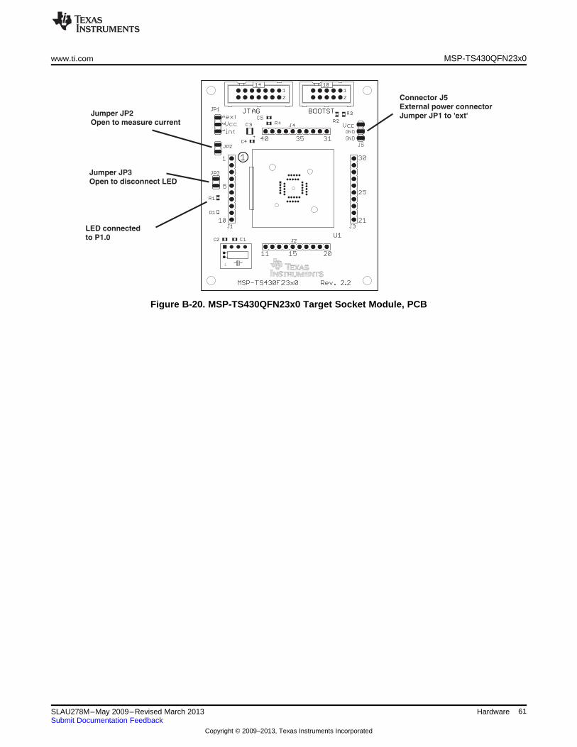
LED connected
to P1.0
Connector J5
External power connector
Jumper JP1 to 'ext'
Jumper JP3
Open to disconnect LED
Jumper JP2
Open to measure current
www.ti.com MSP-TS430QFN23x0
Figure B-20. MSP-TS430QFN23x0 Target Socket Module, PCB
61SLAU278M–May 2009–Revised March 2013 HardwareSubmit Documentation Feedback
Copyright © 2009–2013, Texas Instruments Incorporated
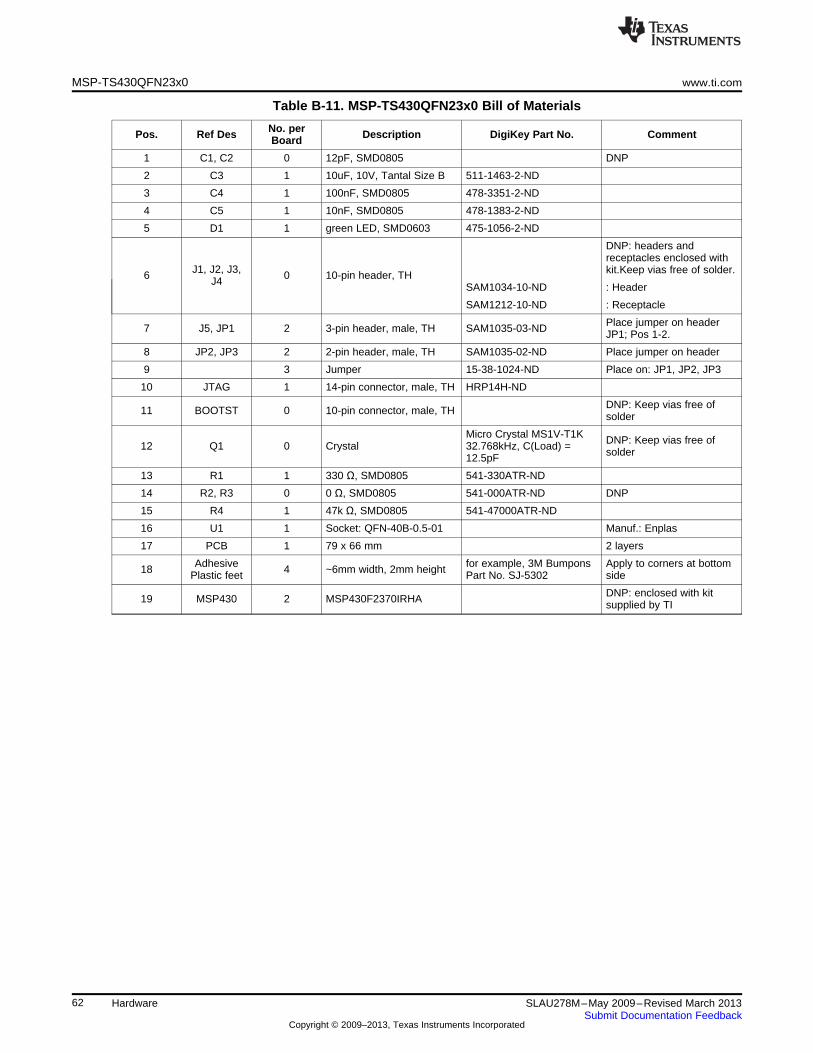
MSP-TS430QFN23x0 www.ti.com
Table B-11. MSP-TS430QFN23x0 Bill of Materials
No. perPos. Ref Des Description DigiKey Part No. CommentBoard
1 C1, C2 0 12pF, SMD0805 DNP
2 C3 1 10uF, 10V, Tantal Size B 511-1463-2-ND
3 C4 1 100nF, SMD0805 478-3351-2-ND
4 C5 1 10nF, SMD0805 478-1383-2-ND
5 D1 1 green LED, SMD0603 475-1056-2-ND
DNP: headers andreceptacles enclosed with
J1, J2, J3, kit.Keep vias free of solder.6 0 10-pin header, THJ4 SAM1034-10-ND : Header
SAM1212-10-ND : Receptacle
Place jumper on header7 J5, JP1 2 3-pin header, male, TH SAM1035-03-ND JP1; Pos 1-2.
8 JP2, JP3 2 2-pin header, male, TH SAM1035-02-ND Place jumper on header
9 3 Jumper 15-38-1024-ND Place on: JP1, JP2, JP3
10 JTAG 1 14-pin connector, male, TH HRP14H-ND
DNP: Keep vias free of11 BOOTST 0 10-pin connector, male, TH solder
Micro Crystal MS1V-T1K DNP: Keep vias free of12 Q1 0 Crystal 32.768kHz, C(Load) = solder12.5pF
13 R1 1 330 Ω, SMD0805 541-330ATR-ND
14 R2, R3 0 0 Ω, SMD0805 541-000ATR-ND DNP
15 R4 1 47k Ω, SMD0805 541-47000ATR-ND
16 U1 1 Socket: QFN-40B-0.5-01 Manuf.: Enplas
17 PCB 1 79 x 66 mm 2 layers
Adhesive for example, 3M Bumpons Apply to corners at bottom18 4 ~6mm width, 2mm heightPlastic feet Part No. SJ-5302 side
DNP: enclosed with kit19 MSP430 2 MSP430F2370IRHA supplied by TI
62 Hardware SLAU278M–May 2009–Revised March 2013Submit Documentation Feedback
Copyright © 2009–2013, Texas Instruments Incorporated
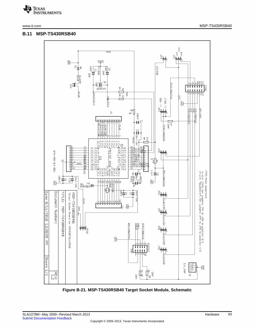
www.ti.com MSP-TS430RSB40
B.11 MSP-TS430RSB40
Figure B-21. MSP-TS430RSB40 Target Socket Module, Schematic
63SLAU278M–May 2009–Revised March 2013 HardwareSubmit Documentation Feedback
Copyright © 2009–2013, Texas Instruments Incorporated

Jumper JP2Open to measure current
Orient Pin 1 of MSP430 device
Jumper JP3Open to disconnect LED
D1 LED connected to P1.0
Jumpers JP4 to JP9Close 1-2 to debug in Spy-Bi-Wire modeClose 2-3 to debug in 4-wire JTAG mode
Connector J5External power connectorJumper JP1 to "ext"
MSP-TS430RSB40 www.ti.com
Figure B-22. MSP-TS430RSB40 Target Socket Module, PCB
64 Hardware SLAU278M–May 2009–Revised March 2013Submit Documentation Feedback
Copyright © 2009–2013, Texas Instruments Incorporated
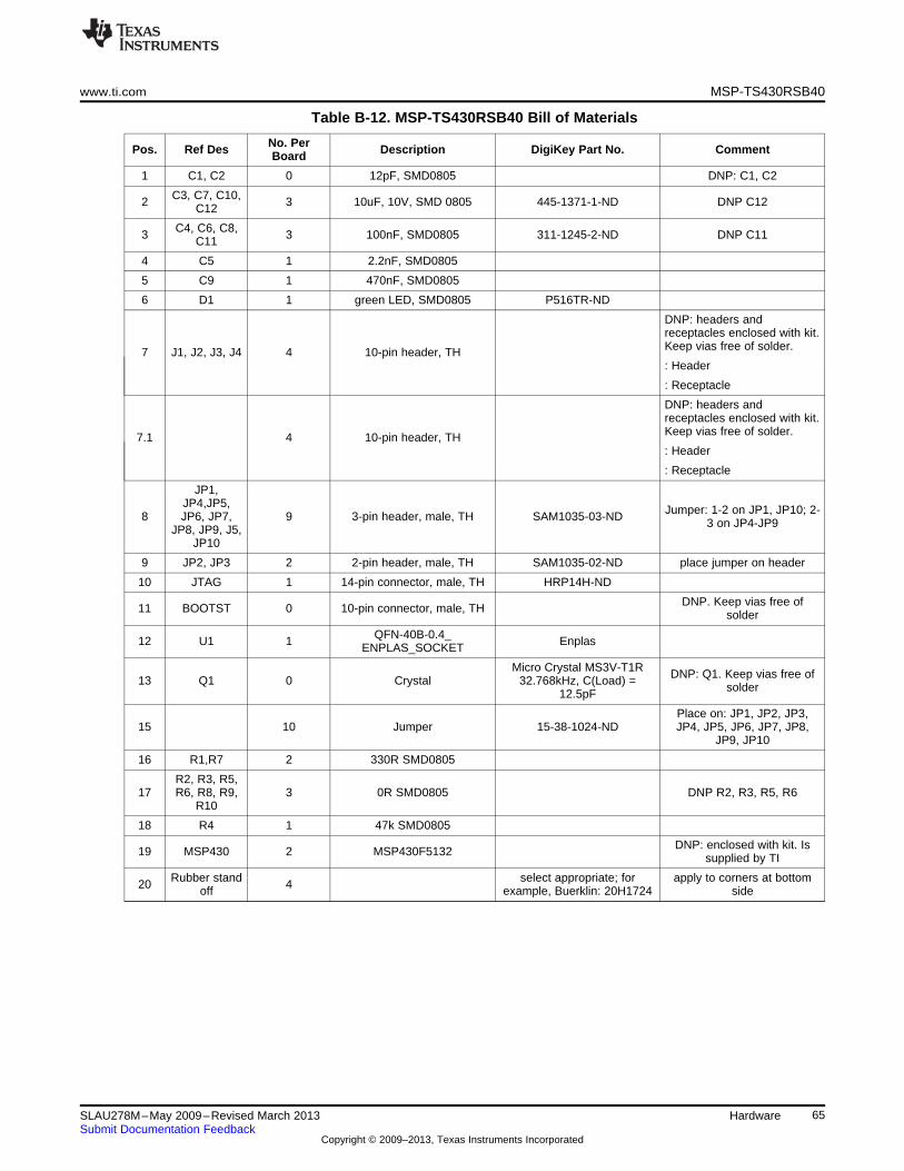
www.ti.com MSP-TS430RSB40
Table B-12. MSP-TS430RSB40 Bill of Materials
No. PerPos. Ref Des Description DigiKey Part No. CommentBoard
1 C1, C2 0 12pF, SMD0805 DNP: C1, C2
C3, C7, C10,2 3 10uF, 10V, SMD 0805 445-1371-1-ND DNP C12C12
C4, C6, C8,3 3 100nF, SMD0805 311-1245-2-ND DNP C11C11
4 C5 1 2.2nF, SMD0805
5 C9 1 470nF, SMD0805
6 D1 1 green LED, SMD0805 P516TR-ND
DNP: headers andreceptacles enclosed with kit.Keep vias free of solder.7 J1, J2, J3, J4 4 10-pin header, TH: Header
: Receptacle
DNP: headers andreceptacles enclosed with kit.Keep vias free of solder.7.1 4 10-pin header, TH: Header
: Receptacle
JP1,JP4,JP5, Jumper: 1-2 on JP1, JP10; 2-8 JP6, JP7, 9 3-pin header, male, TH SAM1035-03-ND 3 on JP4-JP9JP8, JP9, J5,
JP10
9 JP2, JP3 2 2-pin header, male, TH SAM1035-02-ND place jumper on header
10 JTAG 1 14-pin connector, male, TH HRP14H-ND
DNP. Keep vias free of11 BOOTST 0 10-pin connector, male, TH solder
QFN-40B-0.4_12 U1 1 EnplasENPLAS_SOCKET
Micro Crystal MS3V-T1R DNP: Q1. Keep vias free of13 Q1 0 Crystal 32.768kHz, C(Load) = solder12.5pF
Place on: JP1, JP2, JP3,15 10 Jumper 15-38-1024-ND JP4, JP5, JP6, JP7, JP8,
JP9, JP10
16 R1,R7 2 330R SMD0805
R2, R3, R5,17 R6, R8, R9, 3 0R SMD0805 DNP R2, R3, R5, R6
R10
18 R4 1 47k SMD0805
DNP: enclosed with kit. Is19 MSP430 2 MSP430F5132 supplied by TI
Rubber stand select appropriate; for apply to corners at bottom20 4off example, Buerklin: 20H1724 side
65SLAU278M–May 2009–Revised March 2013 HardwareSubmit Documentation Feedback
Copyright © 2009–2013, Texas Instruments Incorporated
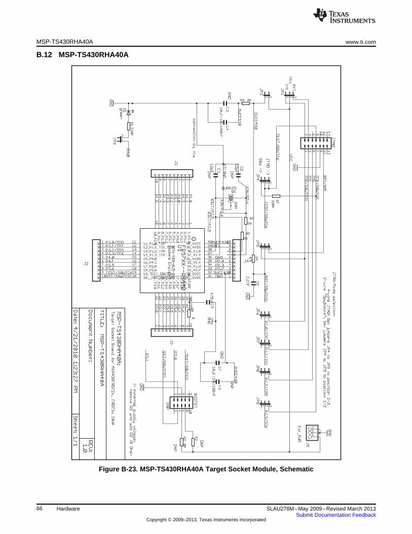
MSP-TS430RHA40A www.ti.com
B.12 MSP-TS430RHA40A
Figure B-23. MSP-TS430RHA40A Target Socket Module, Schematic
66 Hardware SLAU278M–May 2009–Revised March 2013Submit Documentation Feedback
Copyright © 2009–2013, Texas Instruments Incorporated
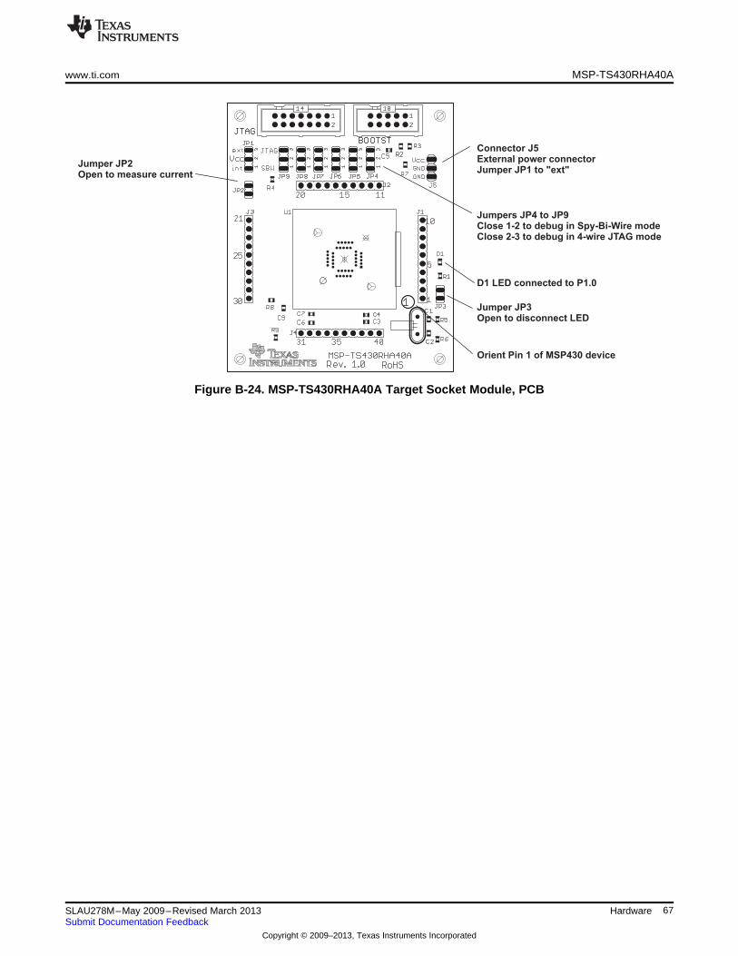
Jumper JP2Open to measure current
Connector J5External power connectorJumper JP1 to "ext"
Jumpers JP4 to JP9Close 1-2 to debug in Spy-Bi-Wire modeClose 2-3 to debug in 4-wire JTAG mode
D1 LED connected to P1.0
Jumper JP3Open to disconnect LED
Orient Pin 1 of MSP430 device
www.ti.com MSP-TS430RHA40A
Figure B-24. MSP-TS430RHA40A Target Socket Module, PCB
67SLAU278M–May 2009–Revised March 2013 HardwareSubmit Documentation Feedback
Copyright © 2009–2013, Texas Instruments Incorporated
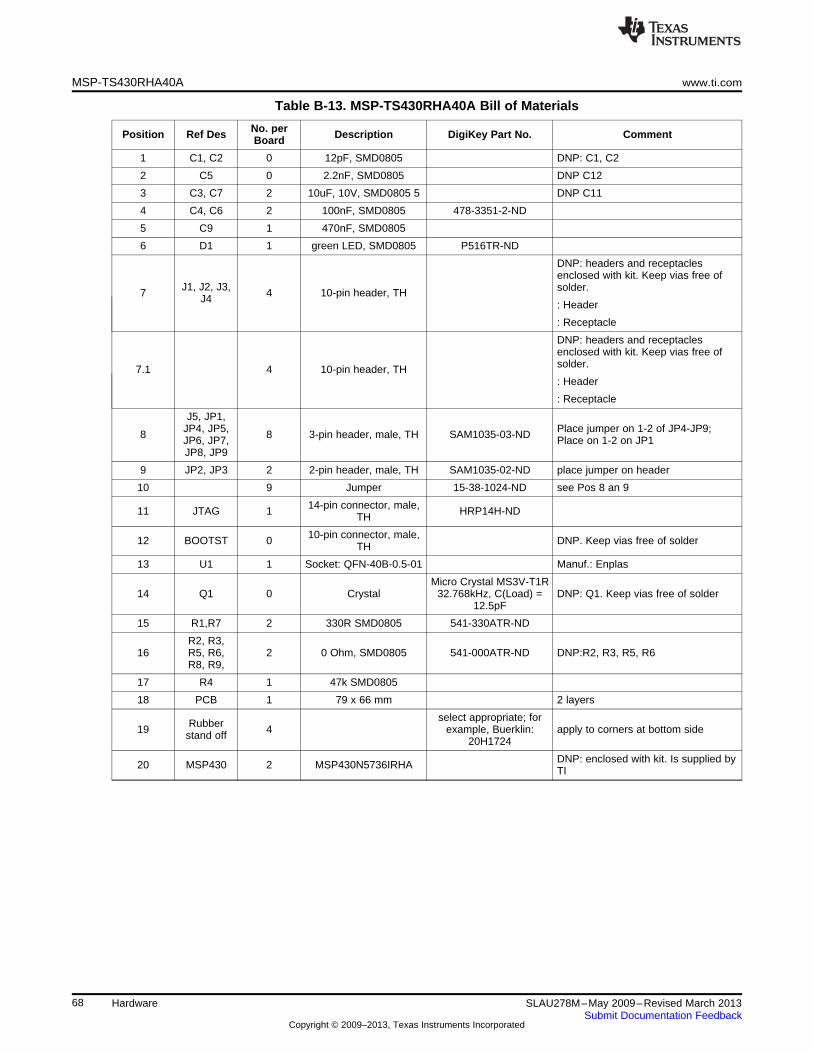
MSP-TS430RHA40A www.ti.com
Table B-13. MSP-TS430RHA40A Bill of Materials
No. perPosition Ref Des Description DigiKey Part No. CommentBoard
1 C1, C2 0 12pF, SMD0805 DNP: C1, C2
2 C5 0 2.2nF, SMD0805 DNP C12
3 C3, C7 2 10uF, 10V, SMD0805 5 DNP C11
4 C4, C6 2 100nF, SMD0805 478-3351-2-ND
5 C9 1 470nF, SMD0805
6 D1 1 green LED, SMD0805 P516TR-ND
DNP: headers and receptaclesenclosed with kit. Keep vias free of
J1, J2, J3, solder.7 4 10-pin header, THJ4 : Header
: Receptacle
DNP: headers and receptaclesenclosed with kit. Keep vias free ofsolder.7.1 4 10-pin header, TH: Header
: Receptacle
J5, JP1,JP4, JP5, Place jumper on 1-2 of JP4-JP9;8 8 3-pin header, male, TH SAM1035-03-NDJP6, JP7, Place on 1-2 on JP1JP8, JP9
9 JP2, JP3 2 2-pin header, male, TH SAM1035-02-ND place jumper on header
10 9 Jumper 15-38-1024-ND see Pos 8 an 9
14-pin connector, male,11 JTAG 1 HRP14H-NDTH
10-pin connector, male,12 BOOTST 0 DNP. Keep vias free of solderTH
13 U1 1 Socket: QFN-40B-0.5-01 Manuf.: Enplas
Micro Crystal MS3V-T1R14 Q1 0 Crystal 32.768kHz, C(Load) = DNP: Q1. Keep vias free of solder
12.5pF
15 R1,R7 2 330R SMD0805 541-330ATR-ND
R2, R3,16 R5, R6, 2 0 Ohm, SMD0805 541-000ATR-ND DNP:R2, R3, R5, R6
R8, R9,
17 R4 1 47k SMD0805
18 PCB 1 79 x 66 mm 2 layers
select appropriate; forRubber19 4 example, Buerklin: apply to corners at bottom sidestand off 20H1724
DNP: enclosed with kit. Is supplied by20 MSP430 2 MSP430N5736IRHA TI
68 Hardware SLAU278M–May 2009–Revised March 2013Submit Documentation Feedback
Copyright © 2009–2013, Texas Instruments Incorporated
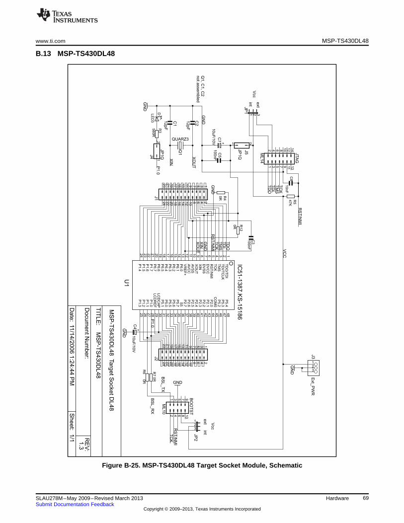
ML
14
LE
D3 1
2p
F
12
pF
GN
D
GND
10
0n
F
560R
ML
10
JP
1Q
JP
1Q
10
uF
/10
V
47K
10nF
0R
0R
GN
D
0R
0R
10
uF
/10
V
GN
D
IC51-1
387.K
S-1
5186
100nF
1.3
MS
P-T
S430D
L48
Targ
et S
ocket D
L48
Q1
, C1
, C2
no
t asse
mb
led
1 3 5 7 9 11
13
2 4 6
12
148
10
JTA
G
D1
C2
C1
C5
R3
BO
OT
ST
12
34
56
78
910
1 2
J5
J4
12
C7
R5
C8
R6 R
7
123
J3
Q1
QUARZ3
J2
135
24679
810
11
13
15
12
14
16
17
19
18
20
21
23
22
24
135
24679
810
11
13
15
12
14
16
17
19
18
20
21
23
22
24
J1
R12
R4
JP
1
1 2 3
123
JP
2
C4
U1
TD
O/T
DI
1
TD
I/TC
LK
2
TM
S3
TC
K4
RS
T/N
MI
5
DV
CC
6
DV
SS
7
XIN
8
XO
UT
9
AV
SS
10
AV
CC
11
VR
EF
+12
P6.0
13
P6.1
14
P6.2
15
P6.3
16
P6.4
17
P6.5
18
P6.6
19
P6.7
20
P2.5
39
P2.4
40
P2.3
41
P2.2
42
P2.1
43
P2.0
44
CO
M0
45
P5.2
46
P5.3
47
P5.4
48
LC
DR
EF
29
LC
DC
AP
30
P5.1
31
P5.0
32
P5.5
33
P5.6
34
P5.7
35
S5
36
P2.7
37
P2.6
38
P1.7
21
P1.6
22
P1.5
23
P1.4
24
P1.0
28
P1.1
27
P1.2
26
P1.3
25
C3
P1
.0
P1
.0
RS
T/N
MI
RS
T/N
MI
RS
T/N
MI
TC
K
TC
K
TC
K
TM
S
TM
S
TD
I
TD
I
TD
O
TD
O
XO
UT
XO
UT
GN
D
GN
DG
ND
XIN
XIN
BS
L_
TX
VC
C
BS
L_
RX
Ext_
PW
R
Date
:11/1
4/2
006 1
:24:4
4 P
MS
heet:
1/1 R
EV
:
TIT
LE
:
Docum
ent N
um
ber:
MS
P-T
S430D
L48
+
+
Vcc
ext
int
int
ext Vcc
www.ti.com MSP-TS430DL48
B.13 MSP-TS430DL48
Figure B-25. MSP-TS430DL48 Target Socket Module, Schematic
69SLAU278M–May 2009–Revised March 2013 HardwareSubmit Documentation Feedback
Copyright © 2009–2013, Texas Instruments Incorporated
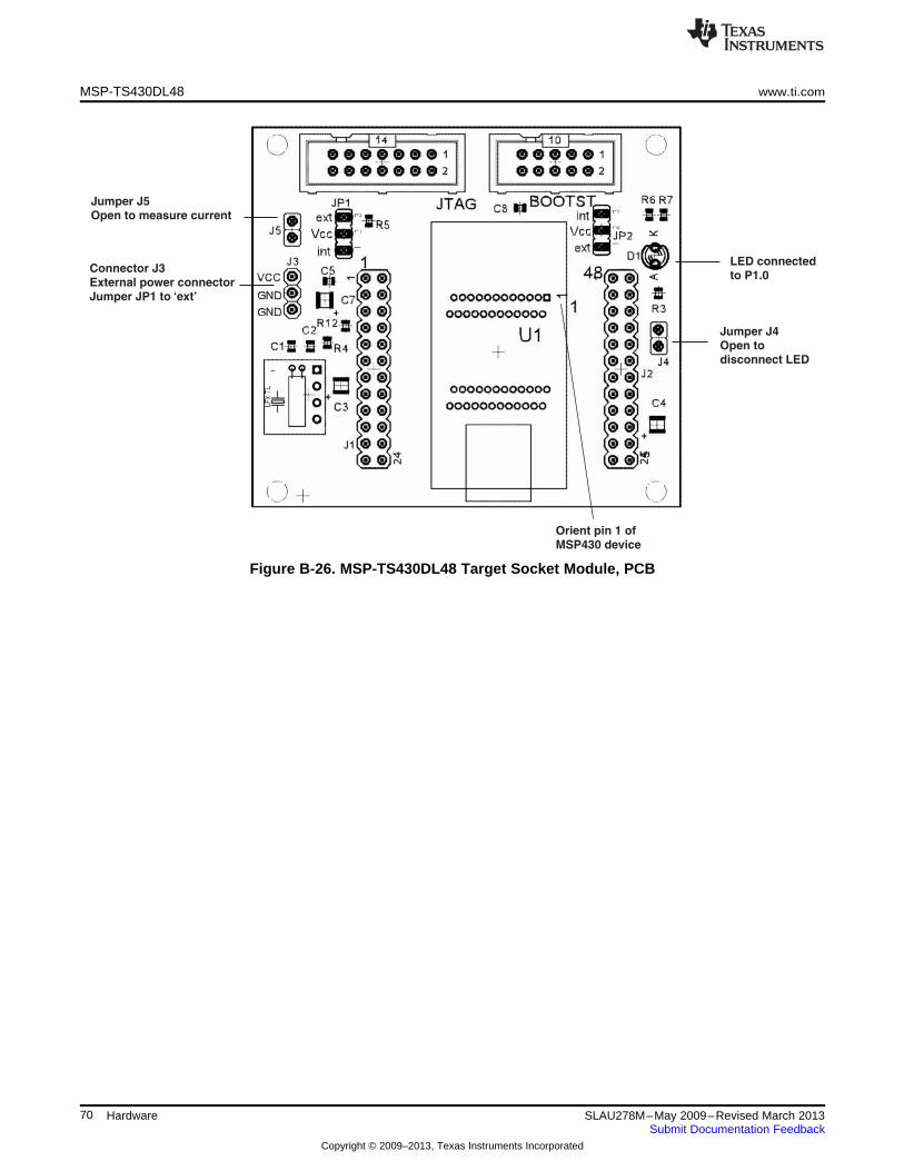
Jumper J4
Open to
disconnect LED
LED connected
to P1.0
Orient pin 1 of
MSP430 device
Jumper J5
Open to measure current
Connector J3
External power connector
Jumper JP1 to ‘ext’
MSP-TS430DL48 www.ti.com
Figure B-26. MSP-TS430DL48 Target Socket Module, PCB
70 Hardware SLAU278M–May 2009–Revised March 2013Submit Documentation Feedback
Copyright © 2009–2013, Texas Instruments Incorporated
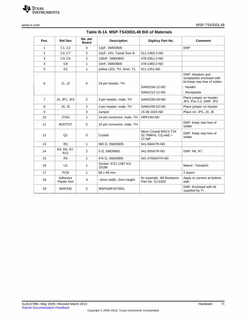
www.ti.com MSP-TS430DL48
Table B-14. MSP-TS430DL48 Bill of Materials
No. perPos. Ref Des Description DigiKey Part No. CommentBoard
1 C1, C2 0 12pF, SMD0805 DNP
2 C4, C7 2 10uF, 10V, Tantal Size B 511-1463-2-ND
3 C3, C5 2 100nF, SMD0805 478-3351-2-ND
4 C8 1 10nF, SMD0805 478-1383-2-ND
5 D1 1 yellow LED, TH, 3mm, T1 511-1251-ND
DNP: Headers andreceptacles enclosed withkit.Keep vias free of solder.6 J1, J2 0 24-pin header, TH
SAM1034-12-ND : Header
SAM1212-12-ND : Receptacle
Place jumper on header7 J3, JP1, JP2 2 3-pin header, male, TH SAM1035-03-ND JP1; Pos 1-2. DNP: JP2
8 J4, J5 2 2-pin header, male, TH SAM1035-02-ND Place jumper on header
9 3 Jumper 15-38-1024-ND Place on: JP1, J4, J5
10 JTAG 1 14-pin connector, male, TH HRP14H-ND
DNP: Keep vias free of11 BOOTST 0 10-pin connector, male, TH solder
Micro Crystal MS1V-T1K DNP: Keep vias free of12 Q1 0 Crystal 32.768kHz, C(Load) = solder12.5pF
13 R3 1 560 Ω, SMD0805 541-560ATR-ND
R4, R6, R7,14 2 0 Ω, SMD0805 541-000ATR-ND DNP: R6, R7R12
15 R5 1 47k Ω, SMD0805 541-47000ATR-ND
Socket: IC51-1387 KS-16 U1 1 Manuf.: Yamaichi15186
17 PCB 1 58 x 66 mm 2 layers
Adhesive for example, 3M Bumpons Apply to corners at bottom18 4 ~6mm width, 2mm heightPlastic feet Part No. SJ-5302 side
DNP: Enclosed with kit19 MSP430 2 MSP430F4270IDL supplied by TI
71SLAU278M–May 2009–Revised March 2013 HardwareSubmit Documentation Feedback
Copyright © 2009–2013, Texas Instruments Incorporated
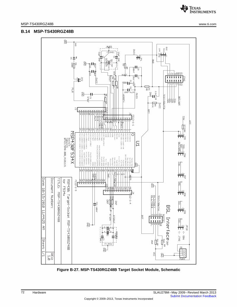
MSP-TS430RGZ48B www.ti.com
B.14 MSP-TS430RGZ48B
Figure B-27. MSP-TS430RGZ48B Target Socket Module, Schematic
72 Hardware SLAU278M–May 2009–Revised March 2013Submit Documentation Feedback
Copyright © 2009–2013, Texas Instruments Incorporated
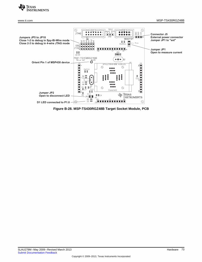
Jumper JP2Open to disconnect LED
Connector J5External power connectorJumper JP1 to "ext"
Jumpers JP5 to JP10Close 1-2 to debug in Spy-Bi-Wire modeClose 2-3 to debug in 4-wire JTAG mode
D1 LED connected to P1.0
Jumper JP1Open to measure current
Orient Pin 1 of MSP430 device
www.ti.com MSP-TS430RGZ48B
Figure B-28. MSP-TS430RGZ48B Target Socket Module, PCB
73SLAU278M–May 2009–Revised March 2013 HardwareSubmit Documentation Feedback
Copyright © 2009–2013, Texas Instruments Incorporated
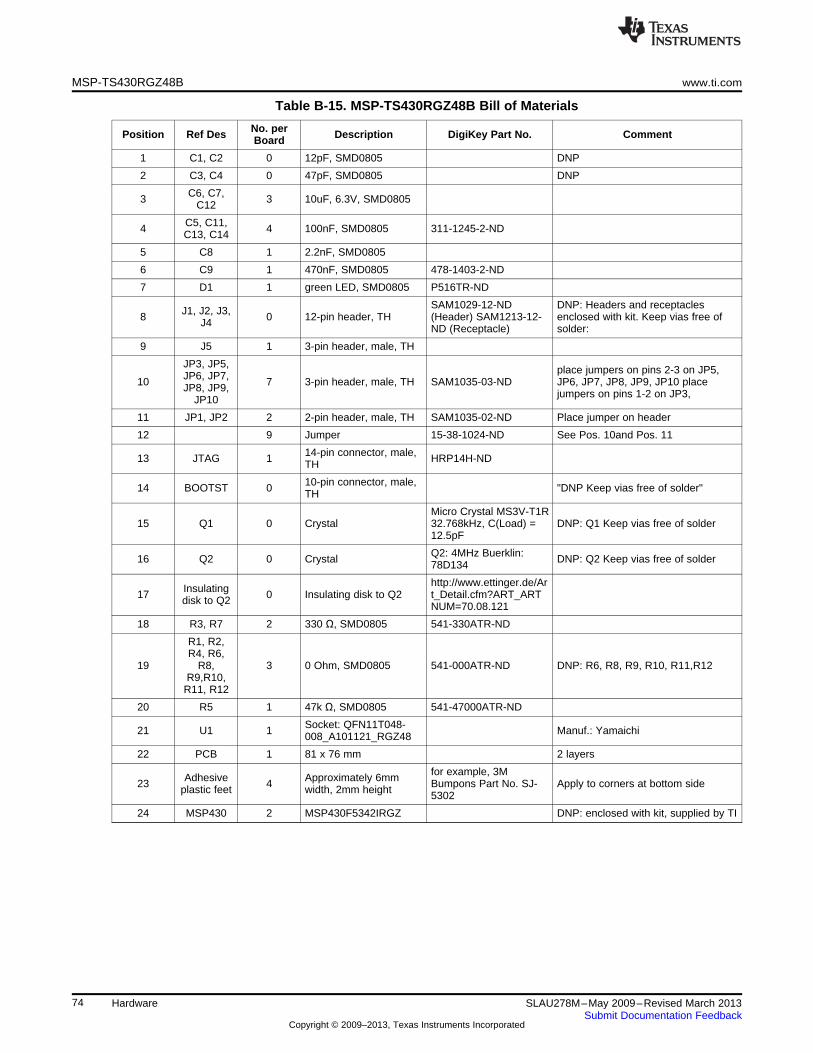
MSP-TS430RGZ48B www.ti.com
Table B-15. MSP-TS430RGZ48B Bill of Materials
No. perPosition Ref Des Description DigiKey Part No. CommentBoard
1 C1, C2 0 12pF, SMD0805 DNP
2 C3, C4 0 47pF, SMD0805 DNP
C6, C7,3 3 10uF, 6.3V, SMD0805C12
C5, C11,4 4 100nF, SMD0805 311-1245-2-NDC13, C14
5 C8 1 2.2nF, SMD0805
6 C9 1 470nF, SMD0805 478-1403-2-ND
7 D1 1 green LED, SMD0805 P516TR-ND
SAM1029-12-ND DNP: Headers and receptaclesJ1, J2, J3,8 0 12-pin header, TH (Header) SAM1213-12- enclosed with kit. Keep vias free ofJ4 ND (Receptacle) solder:
9 J5 1 3-pin header, male, TH
JP3, JP5, place jumpers on pins 2-3 on JP5,JP6, JP7,10 7 3-pin header, male, TH SAM1035-03-ND JP6, JP7, JP8, JP9, JP10 placeJP8, JP9, jumpers on pins 1-2 on JP3,JP10
11 JP1, JP2 2 2-pin header, male, TH SAM1035-02-ND Place jumper on header
12 9 Jumper 15-38-1024-ND See Pos. 10and Pos. 11
14-pin connector, male,13 JTAG 1 HRP14H-NDTH
10-pin connector, male,14 BOOTST 0 "DNP Keep vias free of solder"TH
Micro Crystal MS3V-T1R15 Q1 0 Crystal 32.768kHz, C(Load) = DNP: Q1 Keep vias free of solder
12.5pF
Q2: 4MHz Buerklin:16 Q2 0 Crystal DNP: Q2 Keep vias free of solder78D134
http://www.ettinger.de/ArInsulating17 0 Insulating disk to Q2 t_Detail.cfm?ART_ARTdisk to Q2 NUM=70.08.121
18 R3, R7 2 330 Ω, SMD0805 541-330ATR-ND
R1, R2,R4, R6,
19 R8, 3 0 Ohm, SMD0805 541-000ATR-ND DNP: R6, R8, R9, R10, R11,R12R9,R10,
R11, R12
20 R5 1 47k Ω, SMD0805 541-47000ATR-ND
Socket: QFN11T048-21 U1 1 Manuf.: Yamaichi008_A101121_RGZ48
22 PCB 1 81 x 76 mm 2 layers
for example, 3MAdhesive Approximately 6mm23 4 Bumpons Part No. SJ- Apply to corners at bottom sideplastic feet width, 2mm height 5302
24 MSP430 2 MSP430F5342IRGZ DNP: enclosed with kit, supplied by TI
74 Hardware SLAU278M–May 2009–Revised March 2013Submit Documentation Feedback
Copyright © 2009–2013, Texas Instruments Incorporated
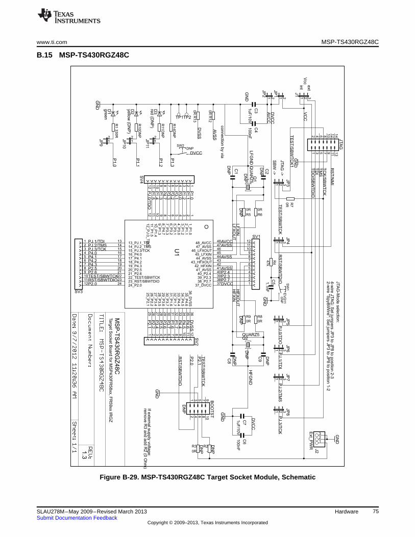
DN
P
DN
P
DN
P
GN
D
GN
D
10
0n
F
330R
-0R
GN
D
GN
D
1.1
nF
47k
GN
D
0R 0R
0R
QU
AR
Z5
1u
F/1
0V
10
0n
F1
uF
/10
V
gre
en
DN
P
yello
w (D
NP
) DN
P
red (D
NP
)
0R
GN
D
DN
P
DN
P
0R0R
QUARZ5
EV
Q11
0R
DNP
DN
P
If exte
rnal s
upply
volta
ge:
rem
ove R
3 a
nd a
dd R
2 (0
Ohm
)
1.3
Ext_
PW
R
MS
P-T
S430R
GZ
48C
Vcc
int
ext
Targ
et S
ocket B
oard
for M
SP
430F
R58xx, F
R59xx IR
GZ
DN
PD
NP
DN
P
DN
P
DN
P
JTA
G ->
SB
W ->
JTA
G-M
ode s
ele
ctio
n:
4-w
ire J
TA
G: S
et ju
mpers
JP
3 to
JP
8 to
positio
n 2
-32-w
ire "S
pyB
iWire
": Set ju
mpers
JP
3 to
JP
8 to
positio
n 1
-2
connectio
n b
y v
ia
DN
P
DN
P
1 3 5 7 9 11
13
2 4 6
12
148
10
JTA
G
C2
C1
C4
R1
12
34
56
78
910
BO
OT
ST
R2R3
123
J2
J1
1 2 3
JP
1
1 2
12J
P9
C5
R4
1 2 3JP
3
1 2 3JP
4
1 2 3JP
5
1 2 3JP
6
1 2 3JP
7
1 2 3JP
8
R5 R6
R7
Q1
C3
C6
C7
D1
R10
12J
P10
D2
R11
12J
P11
D3
R12
JP
2
1 2
C8
C9
R8R9
Q2
SV
4
12345678910
11
12
SV1
123456789
101112
SV
2
1 2 3 4 5 6 7 8 910
11
12
SV3
123456789101112
1_P
1.0
1
2_P
1.1
2
3_P
1.2
3
4_P
3.0
4
5_P
3.1
5
6_P
3.2
6
7_P
3.3
7
8_P
4.7
8
9_P
1.3
9
10_P
1.4
10
11_P
1.5
11
12_P
J.0
_T
DO
12
13_PJ.1_TDI13
14_PJ.2_TMS14
15_PJ.3/TCK15
16_P4.016
17_P4.117
18_P4.218
19_P4.319
20_P2.520
21_P2.621
22_TEST/SBWTCK22
23_RST/SBWTDIO23
24_P2.024
25_P
2.1
25
26_P
2.2
26
27_P
3.4
27
28_P
3.5
28
29_P
3.6
29
30_P
3.7
30
31_P
1.6
31
32_P
1.7
32
33_P
4.4
33
34_P
4.5
34
35_P
4.6
35
36_D
VS
S36
37_DVCC 3738_P2.7 3839_P2.3 3940_P2.4 40
41_AVSS 4142_HFXIN 42
43_HFXOUT 4344_AVSS 4445_LFXIN 45
46_LFXOUT 4647_AVSS 4748_AVCC 48
U1
SW
1
R13
TP2TP1
SW2
R14
P1.0
P1.0
RS
T/N
MI
TM
ST
DI
VC
C
GN
D
P1.1
P1.1
RS
T/S
BW
TD
IO
RS
T/S
BW
TD
IORST/SBWTDIO
TC
K/S
BW
TC
K
TD
O/S
BW
TD
IO
PJ.0
/TD
O
PJ.0
/TD
O
PJ.2
/TM
S
PJ.2/TMS
PJ.3
/TC
K
PJ.3/TCK
PJ.1
/TD
I
PJ.1/TDI
P1.2
P1.2
P2.0
P2.0
P2.1
P2.1
P1.3
P1.3
P1.4
P1.5
AVCC
AV
CC
AVSS
AV
SS
AVSS
AVSS
LF
XO
UT
LF
XIN
LF
GN
DH
FG
ND
HF
XO
UT
HF
XIN
P2.4P2.3P2.7DVCC
DV
CC
DV
CC
DVCC
DV
SS
DV
SS
P4.6
P4.5
P4.4
P1.7
P1.6
P3.7
P3.6
P3.5
P3.4
P2.2
P2.6P2.5P4.3P4.2P4.1P4.0
P4.7
P3.3
P3.2
P3.1
P3.0
TE
ST
/SB
WT
CK
1
TEST/SBWTCK
TE
ST
/SB
WT
CK
TE
ST
/SB
WT
CK
www.ti.com MSP-TS430RGZ48C
B.15 MSP-TS430RGZ48C
Figure B-29. MSP-TS430RGZ48C Target Socket Module, Schematic
75SLAU278M–May 2009–Revised March 2013 HardwareSubmit Documentation Feedback
Copyright © 2009–2013, Texas Instruments Incorporated
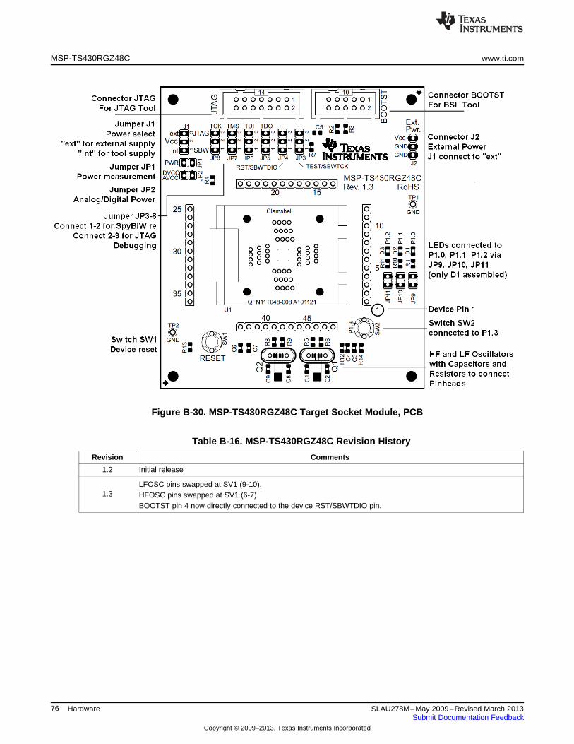
MSP-TS430RGZ48C www.ti.com
Figure B-30. MSP-TS430RGZ48C Target Socket Module, PCB
Table B-16. MSP-TS430RGZ48C Revision History
Revision Comments
1.2 Initial release
LFOSC pins swapped at SV1 (9-10).1.3 HFOSC pins swapped at SV1 (6-7).
BOOTST pin 4 now directly connected to the device RST/SBWTDIO pin.
76 Hardware SLAU278M–May 2009–Revised March 2013Submit Documentation Feedback
Copyright © 2009–2013, Texas Instruments Incorporated
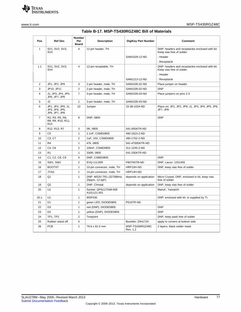
www.ti.com MSP-TS430RGZ48C
Table B-17. MSP-TS430RGZ48C Bill of Materials
NumberPos Ref Des Per Description DigiKey Part Number Comment
Board
1 SV1, SV2, SV3, 4 12-pin header, TH DNP: headers and receptacles enclosed with kit.SV4 Keep vias free of solder.
SAM1029-12-ND : Header
: Receptacle
1.1 SV1, SV2, SV3, 4 12-pin receptable, TH DNP: headers and receptacles enclosed with kit.SV4 Keep vias free of solder.
: Header
SAM1213-12-ND : Receptacle
2 JP1, JP2, JP9 3 2-pin header, male, TH SAM1035-02-ND Place jumper on header
3 JP10, JP11 2 2-pin header, male, TH SAM1035-02-ND DNP
4 J1, JP3, JP4, JP5, 7 3-pin header, male, TH SAM1035-03-ND Place jumpers on pins 2-3JP6, JP7, JP8
5 J2 1 3-pin header, male, TH SAM1035-03-ND
6 JP1, JP2, JP9, J1, 10 Jumper 15-38-1024-ND Place on: JP1, JP2, JP9, J1, JP3, JP4, JP5, JP6,JP3, JP4, JP5, JP7, JP8JP6, JP7, JP8
7 R2, R3, R5, R6, 9 DNP, 0805 DNPR8, R9, R10, R11,R14
8 R12, R13, R7 3 0R, 0805 541-000ATR-ND
9 C5 1 1.1nF, CSMD0805 490-1623-2-ND
10 C3, C7 2 1uF, 10V, CSMD0805 490-1702-2-ND
11 R4 1 47k, 0805 541-47000ATR-ND
12 C4, C6 2 100nF, CSMD0805 311-1245-2-ND
13 R1 1 330R, 0805 541-330ATR-ND
14 C1, C2, C8, C9 4 DNP, CSMD0805 DNP
15 SW1, SW2 2 EVQ-11L05R P8079STB-ND DNP, Lacon: 1251459
16 BOOTST 1 10-pin connector, male, TH HRP10H-ND DNP, keep vias free of solder
17 JTAG 1 14-pin connector, male, TH HRP14H-ND
18 Q1 1 DNP: MS3V-TR1 (32768kHz, depends on application Micro Crystal, DNP, enclosed in kit, keep vias20ppm, 12.5pF) free of solder
19 Q2 1 DNP, Christal depends on application DNP, keep vias free of solder
20 U1 1 Socket: QFN11T048-008 Manuf.: YamaichiA101121-001
20.1 U1 1 MSP430 DNP: enclosed with kit. Is supplied by TI.
21 D1 1 green LED, DIODE0805 P516TR-ND
22 D3 1 red (DNP), DIODE0805 DNP
23 D2 1 yellow (DNP), DIODE0805 DNP
24 TP1, TP2 2 Testpoint DNP, keep pads free of solder
25 Rubber stand off 4 Buerklin: 20H1724 apply to corners at bottom side
26 PCB 1 79.6 x 91.0 mm MSP-TS430RGZ48C 2 layers, black solder maskRev. 1.2
77SLAU278M–May 2009–Revised March 2013 HardwareSubmit Documentation Feedback
Copyright © 2009–2013, Texas Instruments Incorporated
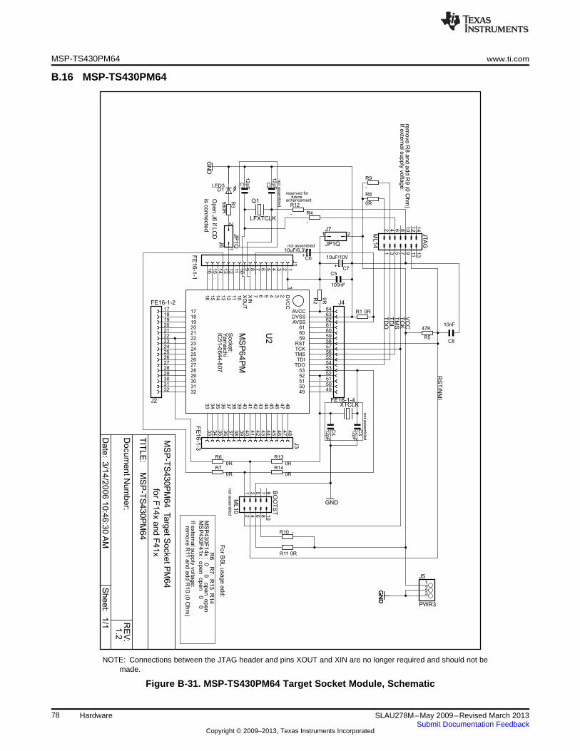
ML
14
LED3
0R
12
pF
12
pF
12
pF
12
pF
GN
D
GND
0R
100nF
56
0R
ML
10
JP1Q
JP
1Q
10uF/6,3V
10uF/10V
47K10nF
0R
0R
0R
-
-
0R
-
0R
0R
FE
16
-1-1
FE16-1-2
FE
16
-1-3
FE16-1-4
PWR3
GN
DG
ND
-
MS
P6
4P
M
not assembled
not a
ssem
ble
d
not a
ssem
ble
d
not a
ssem
ble
d
enhancement
reserved forfuture
JTA
G
1 3 5 7 9 11
13
2 4 6
12
148
10
D1
R2
C2
C1
C3
C4
R1
C5
R3
BO
OT
ST
12
34
56
78
91
0
J71 2
J6
12
C6
C7
R5C8
R6
R7
R8
R9
R10
R11
R12
R13
R14
12345678910
11
12
13
14
15
16
J1
J2
17181920212223242526272829303132
J3
33
34
35
36
37
38
39
40
41
42
43
44
45
46
47
48
49505152535455565758596061626364
J4
J5123
R4
Q1
LFXTCLK
XTCLK
U2
DV
CC
234567XIN
XO
UT
10
11
12
13
14
15
16
17181920212223242526272829303132
33
34
35
36
37
38
39
40
41
42
43
44
45
46
47
48
4950515253
TDOTDI
TMSTCKRST
596061
AVSSDVSSAVCC
RS
T/N
MI
TC
KT
MS
TD
IT
DO
VC
C
Da
te:
3/1
4/2
00
6 1
0:4
6:3
0A
MS
he
et:
1/1 R
EV
:
TIT
LE
:
Do
cu
me
nt N
um
be
r:
MS
P-T
S4
30
PM
64
+
+
1
MS
P-T
S4
30
PM
64
Ta
rge
t So
cke
t PM
64
Ya
ma
ich
iIC
51
-06
44
-80
7
So
cke
t:
1.2
for F
14
x a
nd
F4
1x
Op
en
J6
if LC
D
is c
on
ne
cte
d
If exte
rna
l su
pp
ly v
olta
ge
:re
mo
ve
R8
an
d a
dd
R9
(0 O
hm
)
If exte
rna
l su
pp
ly v
olta
ge
:re
mo
ve
R11
an
d a
dd
R1
0 (0
Oh
m)
Fo
r BS
Lu
sa
ge
ad
d:
R6
R7
R1
3 R
14
MS
P4
30
F1
4x : 0
0 o
pe
n o
pe
nM
SP
43
0F
41
x : o
pe
n o
pe
n 0
0
MSP-TS430PM64 www.ti.com
B.16 MSP-TS430PM64
NOTE: Connections between the JTAG header and pins XOUT and XIN are no longer required and should not bemade.
Figure B-31. MSP-TS430PM64 Target Socket Module, Schematic
78 Hardware SLAU278M–May 2009–Revised March 2013Submit Documentation Feedback
Copyright © 2009–2013, Texas Instruments Incorporated
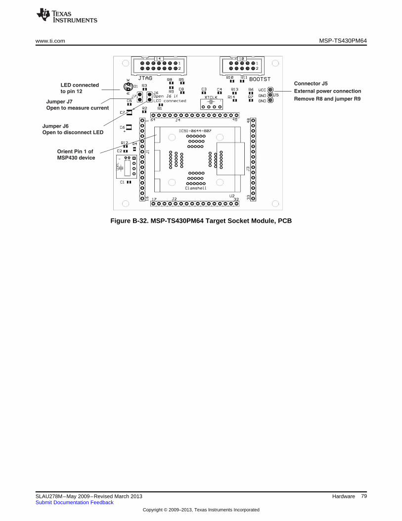
Connector J5
External power connection
Remove R8 and jumper R9
LED connected
to pin 12
Jumper J6
Open to disconnect LED
Jumper J7
Open to measure current
Orient Pin 1 of
MSP430 device
www.ti.com MSP-TS430PM64
Figure B-32. MSP-TS430PM64 Target Socket Module, PCB
79SLAU278M–May 2009–Revised March 2013 HardwareSubmit Documentation Feedback
Copyright © 2009–2013, Texas Instruments Incorporated
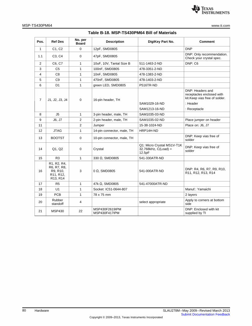
MSP-TS430PM64 www.ti.com
Table B-18. MSP-TS430PM64 Bill of Materials
No. perPos. Ref Des Description DigiKey Part No. CommentBoard
1 C1, C2 0 12pF, SMD0805 DNP
DNP: Only recommendation.1.1 C3, C4 0 47pF, SMD0805 Check your crystal spec.
2 C6, C7 1 10uF, 10V, Tantal Size B 511-1463-2-ND DNP: C6
3 C5 1 100nF, SMD0805 478-3351-2-ND
4 C8 1 10nF, SMD0805 478-1383-2-ND
5 C9 1 470nF, SMD0805 478-1403-2-ND
6 D1 1 green LED, SMD0805 P516TR-ND
DNP: Headers andreceptacles enclosed withkit.Keep vias free of solder.7 J1, J2, J3, J4 0 16-pin header, TH
SAM1029-16-ND : Header
SAM1213-16-ND : Receptacle
8 J5 1 3-pin header, male, TH SAM1035-03-ND
9 J6, J7 2 2-pin header, male, TH SAM1035-02-ND Place jumper on header
11 2 Jumper 15-38-1024-ND Place on: J6, J7
12 JTAG 1 14-pin connector, male, TH HRP14H-ND
DNP: Keep vias free of13 BOOTST 0 10-pin connector, male, TH solder
Q1: Micro Crystal MS1V-T1K DNP: Keep vias free of14 Q1, Q2 0 Crystal 32.768kHz, C(Load) = solder12.5pF
15 R3 1 330 Ω, SMD0805 541-330ATR-ND
R1, R2, R4,R6, R7, R8, DNP: R4, R6, R7, R9, R10,16 R9, R10, 3 0 Ω, SMD0805 541-000ATR-ND R11, R12, R13, R14R11, R12,R13, R14
17 R5 1 47k Ω, SMD0805 541-47000ATR-ND
18 U1 1 Socket: IC51-0644-807 Manuf.: Yamaichi
19 PCB 1 78 x 75 mm 2 layers
Rubber Apply to corners at bottom20 4 select appropriatestandoff side
MSP430F2619IPM DNP: Enclosed with kit21 MSP430 22 MSP430F417IPM supplied by TI
80 Hardware SLAU278M–May 2009–Revised March 2013Submit Documentation Feedback
Copyright © 2009–2013, Texas Instruments Incorporated
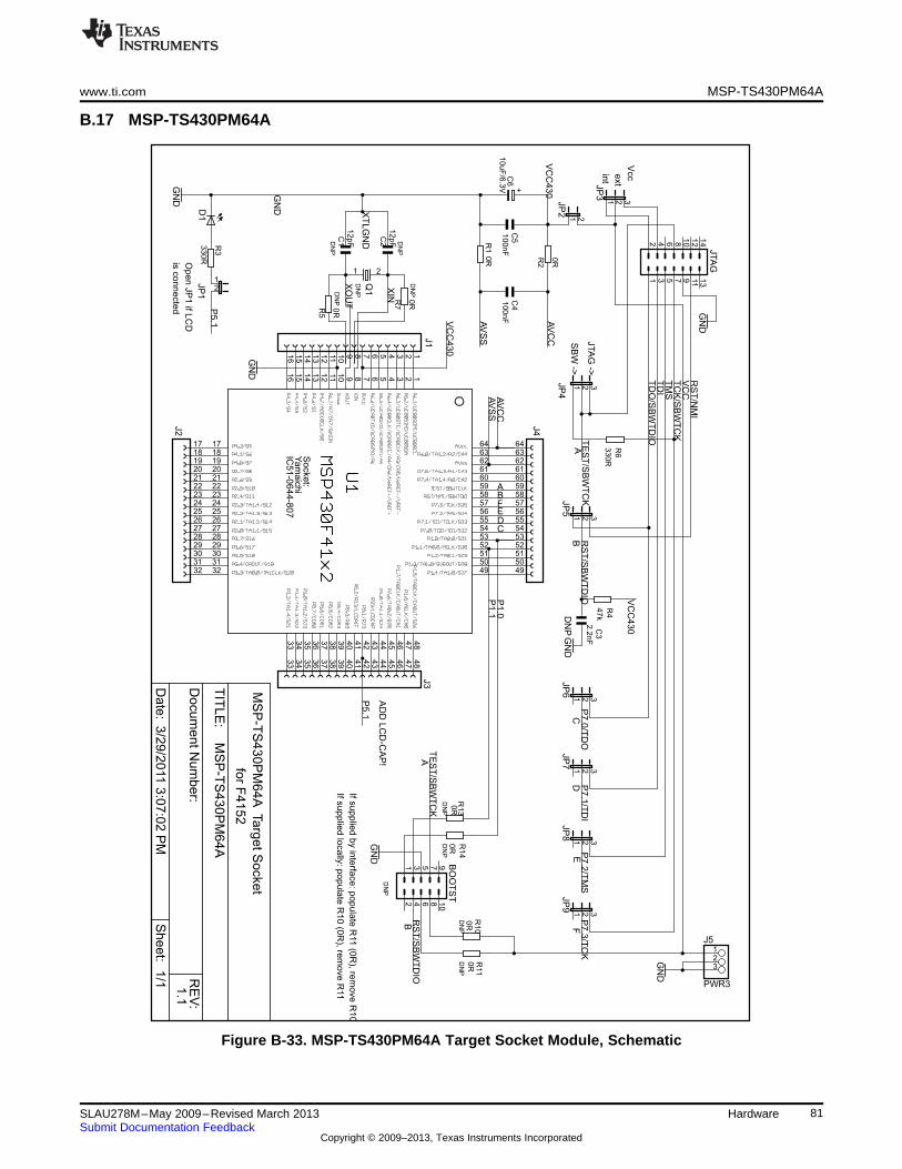
0R
12
pF
12
pF
GN
D
GN
D
0R
10
0n
F
33
0R
10
uF
/6.3
V
0R
0R
0R
0R
PWR3
GN
D
47
k
2.2
nF
33
0R
GN
D
GN
D
10
0n
F
GN
D
0R
0R
MS
P-T
S4
30
PM
64
ATa
rge
t So
cke
t
DN
P
Yam
aic
hi
IC51-0
644-8
07
Socket:
DN
P
1.1
for F
41
52
Open J
P1 if L
CD
is c
onnecte
d
JTA
G ->
SB
W ->
DN
P
DN
P
DN
P
DN
PD
NP
DN
PD
NP
Vccext
int
TE
ST
/SB
WT
CK
RS
T/S
BW
TD
IOP
7.0
/TD
OP
7.1
/TD
IP
7.2
/TM
SP
7.3
/TC
K
AD
D L
CD
-CA
P!
DN
PDN
P
JTA
G
1 3 5 7 9 11
13
2 4 6
12
148
10
R2
C2
C1 R
1
C5
R3
BO
OT
ST
12
34
56
78
91
0
C6
R1
0R
11
R1
3R
14
12345678910
11
12
13
14
15
16
J1
17181920212223242526272829303132
J2
J3
33
34
35
36
37
38
39
40
41
42
43
44
45
46
47
48
49505152535455565758596061626364
J4
J5123
48
47
46
45
44
43
42
41
40
39
38
37
36
35
34
33
32313029282726252423222120191817
16 12345678911
12
13
14
15
10
64636261605958575655545352515049
21
Q1
R4
C3
1 2 3JP
4JP
5
1 2 3
JP
6
1 2 3
JP
7
1 2 3
JP
8
1 2 3
R6
JP
9
1 2 3
12
JP
1
JP
2
1 2
JP
3
1 2 3
D1
C4R
5
R7
RS
T/N
MI
TM
ST
DI
VC
C
GN
D XT
LG
ND
TC
K/S
BW
TC
K
TD
O/S
BW
TD
IO
VC
C430
VC
C430
VC
C430
P5.1
P5.1 A
VC
C
AV
CC
AV
SS
AV
SS
P1.0
P1.1
XIN
XO
UT
A
AA
B
BB
C
C
D
D
E
E
F
F
Da
te:
3/2
9/2
011
3:0
7:0
2 P
MS
he
et:
1/1 R
EV
:
TIT
LE
:
Do
cu
me
nt N
um
be
r:
MS
P-T
S4
30
PM
64
A
+
TE
ST
/SB
WT
CK
RS
T/S
BW
TD
IO
If supplie
d lo
cally
: popula
te R
10 (0
R), re
move R
11
If supplie
d b
y in
terfa
ce: p
opula
te R
11 (0
R), re
move R
10
www.ti.com MSP-TS430PM64A
B.17 MSP-TS430PM64A
Figure B-33. MSP-TS430PM64A Target Socket Module, Schematic
81SLAU278M–May 2009–Revised March 2013 HardwareSubmit Documentation Feedback
Copyright © 2009–2013, Texas Instruments Incorporated
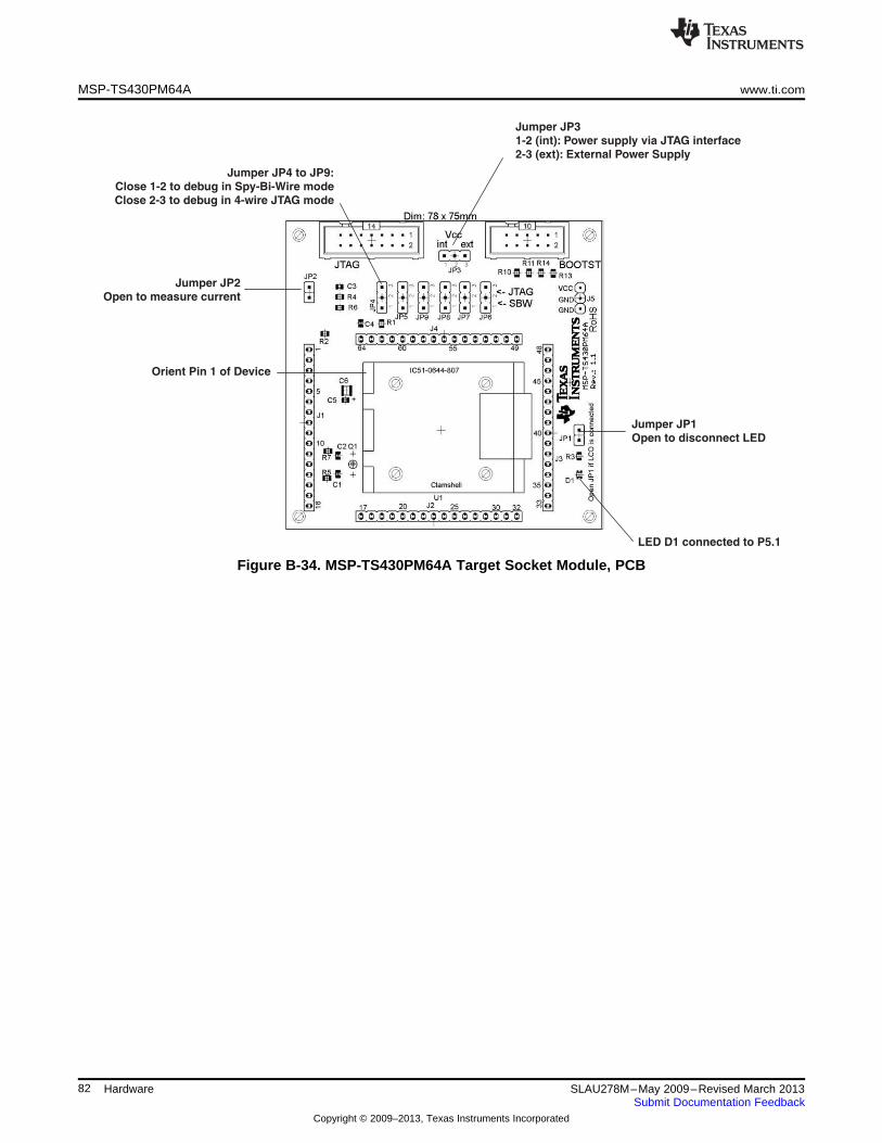
Jumper JP2Open to measure current
Jumper JP1Open to disconnect LED
LED D1 connected to P5.1
Jumper JP31-2 (int): Power supply via JTAG interface2-3 (ext): External Power Supply
Jumper JP4 to JP9:Close 1-2 to debug in Spy-Bi-Wire modeClose 2-3 to debug in 4-wire JTAG mode
Orient Pin 1 of Device
MSP-TS430PM64A www.ti.com
Figure B-34. MSP-TS430PM64A Target Socket Module, PCB
82 Hardware SLAU278M–May 2009–Revised March 2013Submit Documentation Feedback
Copyright © 2009–2013, Texas Instruments Incorporated
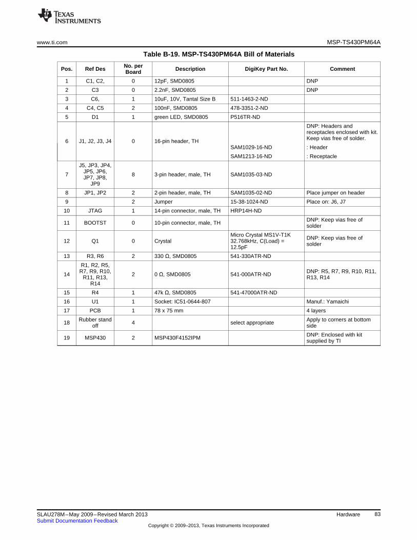
www.ti.com MSP-TS430PM64A
Table B-19. MSP-TS430PM64A Bill of Materials
No. perPos. Ref Des Description DigiKey Part No. CommentBoard
1 C1, C2, 0 12pF, SMD0805 DNP
2 C3 0 2.2nF, SMD0805 DNP
3 C6, 1 10uF, 10V, Tantal Size B 511-1463-2-ND
4 C4, C5 2 100nF, SMD0805 478-3351-2-ND
5 D1 1 green LED, SMD0805 P516TR-ND
DNP: Headers andreceptacles enclosed with kit.Keep vias free of solder.6 J1, J2, J3, J4 0 16-pin header, TH
SAM1029-16-ND : Header
SAM1213-16-ND : Receptacle
J5, JP3, JP4,JP5, JP6,7 8 3-pin header, male, TH SAM1035-03-NDJP7, JP8,
JP9
8 JP1, JP2 2 2-pin header, male, TH SAM1035-02-ND Place jumper on header
9 2 Jumper 15-38-1024-ND Place on: J6, J7
10 JTAG 1 14-pin connector, male, TH HRP14H-ND
DNP: Keep vias free of11 BOOTST 0 10-pin connector, male, TH solder
Micro Crystal MS1V-T1K DNP: Keep vias free of12 Q1 0 Crystal 32.768kHz, C(Load) = solder12.5pF
13 R3, R6 2 330 Ω, SMD0805 541-330ATR-ND
R1, R2, R5,R7, R9, R10, DNP: R5, R7, R9, R10, R11,14 2 0 Ω, SMD0805 541-000ATR-NDR11, R13, R13, R14
R14
15 R4 1 47k Ω, SMD0805 541-47000ATR-ND
16 U1 1 Socket: IC51-0644-807 Manuf.: Yamaichi
17 PCB 1 78 x 75 mm 4 layers
Rubber stand Apply to corners at bottom18 4 select appropriateoff side
DNP: Enclosed with kit19 MSP430 2 MSP430F4152IPM supplied by TI
83SLAU278M–May 2009–Revised March 2013 HardwareSubmit Documentation Feedback
Copyright © 2009–2013, Texas Instruments Incorporated
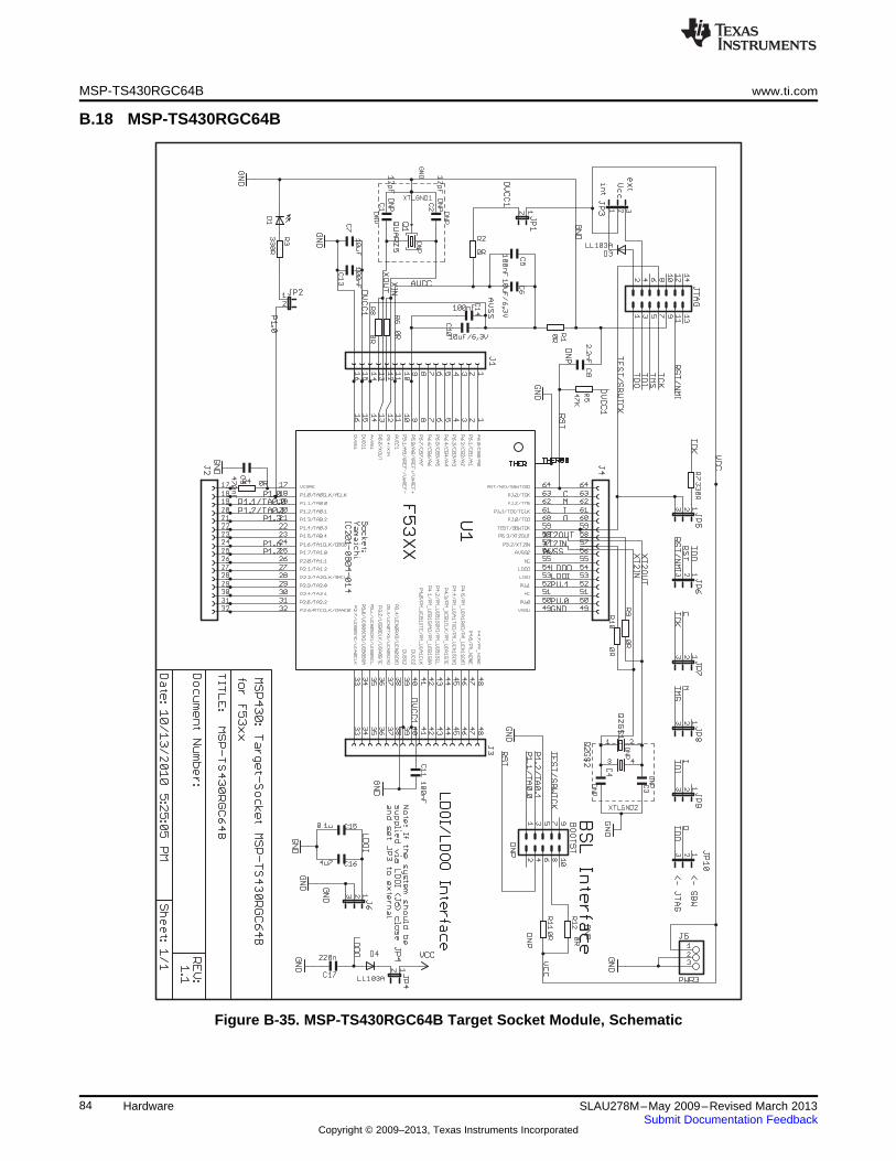
MSP-TS430RGC64B www.ti.com
B.18 MSP-TS430RGC64B
Figure B-35. MSP-TS430RGC64B Target Socket Module, Schematic
84 Hardware SLAU278M–May 2009–Revised March 2013Submit Documentation Feedback
Copyright © 2009–2013, Texas Instruments Incorporated
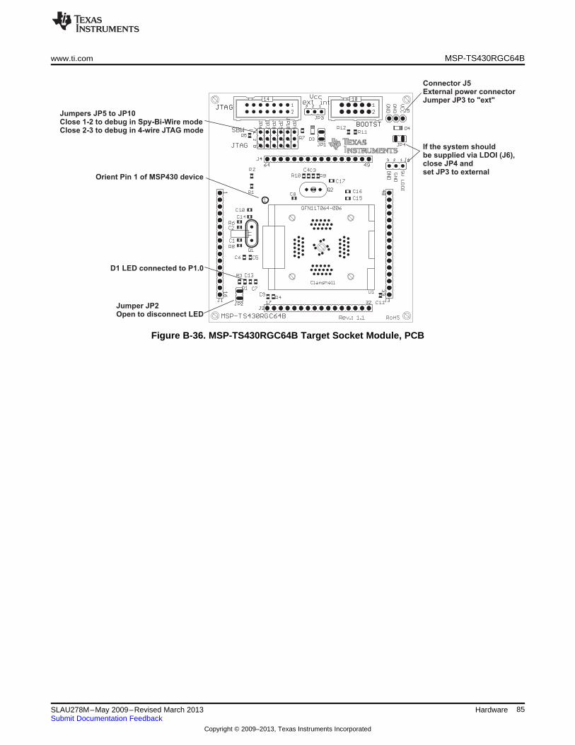
Jumper JP2Open to disconnect LED
Connector J5External power connectorJumper JP3 to "ext"
Jumpers JP5 to JP10Close 1-2 to debug in Spy-Bi-Wire modeClose 2-3 to debug in 4-wire JTAG mode
D1 LED connected to P1.0
If the system shouldbe supplied via LDOI (J6),close JP4 andset JP3 to external
Orient Pin 1 of MSP430 device
www.ti.com MSP-TS430RGC64B
Figure B-36. MSP-TS430RGC64B Target Socket Module, PCB
85SLAU278M–May 2009–Revised March 2013 HardwareSubmit Documentation Feedback
Copyright © 2009–2013, Texas Instruments Incorporated

MSP-TS430RGC64B www.ti.com
Table B-20. MSP-TS430RGC64B Bill of Materials
No. perPos. Ref Des Description DigiKey Part No. CommentBoard
1 C1, C2 0 12pF, SMD0805 DNP
2 C3, C4 0 47pF, SMD0805 DNP
3 C6, C7, C10 3 10uF, 6.3V, SMD0805
C5, C11,4 C13, C14, 5 100nF, SMD0805 311-1245-2-ND
C15
5 C8 1 2.2nF, SMD0805
6 C9 1 470nF, SMD0805 478-1403-2-ND
7 C16 1 4.7uF, SMD0805
8 C17 1 220nF, SMD0805
9 D1 1 green LED, SMD0805 P516TR-ND
SAM1029-16-ND DNP: Headers and receptaclesJ1, J2, J3,10 0 16-pin header, TH (Header) SAM1213-16- enclosed with kit. Keep vias free ofJ4 ND (Receptacle) solder:
11 J5 , J6 2 3-pin header, male, TH
JP3, JP5, place jumpers on pins 2-3 on JP5, JP6,JP6, JP7,12 7 3-pin header, male, TH SAM1035-03-ND JP7, JP8, JP9, JP10 place jumpers onJP8, JP9, pins 1-2 on JP3,JP10
JP1, JP2,13 3 2-pin header, male, TH SAM1035-02-ND Place jumper on headerJP4
14 10 Jumper 15-38-1024-ND See Pos. 12 and Pos. 13
14-pin connector, male,15 JTAG 1 HRP14H-NDTH
10-pin connector, male,16 BOOTST 0 "DNP Keep vias free of solder"TH
Micro Crystal MS3V-T1R17 Q1 0 Crystal 32.768kHz, C(Load) = DNP: Q1 Keep vias free of solder
12.5pF
Q2: 4MHz Buerklin:18 Q2 0 Crystal DNP: Q2 Keep vias free of solder78D134
http://www.ettinger.de/ArtInsulating19 0 Insulating disk to Q2 _Detail.cfm?ART_ARTNUdisk to Q2 M=70.08.121
20 R3, R7 2 330 Ω, SMD0805 541-330ATR-ND
R1, R2, R4,R6, R8,21 3 0 Ohm, SMD0805 541-000ATR-ND DNP: R6, R8, R9, R10, R11,R12R9,R10,
R11, R12
22 R5 1 47k Ω, SMD0805 541-47000ATR-ND
Socket: QFN11T064-006-23 U1 1 Manuf.: YamaichiN-HSP
24 PCB 1 85 x 76 mm 2 layers
for example, 3MAdhesive Approximately 6mm25 4 Bumpons Part No. SJ- Apply to corners at bottom sideplastic feet width, 2mm height 5302
26 D3,D4
27 MSP430 2 MSP430F5310 RGC DNP: enclosed with kit, supplied by TI
86 Hardware SLAU278M–May 2009–Revised March 2013Submit Documentation Feedback
Copyright © 2009–2013, Texas Instruments Incorporated
www.ti.com MSP-TS430RGC64C
B.19 MSP-TS430RGC64C
The MSP-TS430RGC64C target board has been designed to operate with the target device DVIO inputvoltage supplied via header J6 (see Figure B-37). This development platform does not supply the 1.8-VDVIO rail on board and it MUST be provided by external power supply for proper device operation. Forcorrect JTAG connection, programming, and debug operation, it is important to follow this procedure:
1. Make sure that the VCC and DVIO voltage supplies are OFF and that the power rails are fullydischarged to 0 V.
2. Enable the 1.8-V external DVIO power supply.
3. Enable the 1.8-V to 3.6-V VCC power supply (alternatively, this supply can be provided from the MSP-FET430UIF JTAG debugger interface).
4. Connect the MSP-FET430UIF JTAG connector to the target board.
5. Start the debug session using IAR or CCS IDE.
For more information on debugging the MSP430F522x, see the device data sheet (SLAS718) andDesigning with MSP430F522x and MSP430F521x Devices (SLAA558).
87SLAU278M–May 2009–Revised March 2013 HardwareSubmit Documentation Feedback
Copyright © 2009–2013, Texas Instruments Incorporated
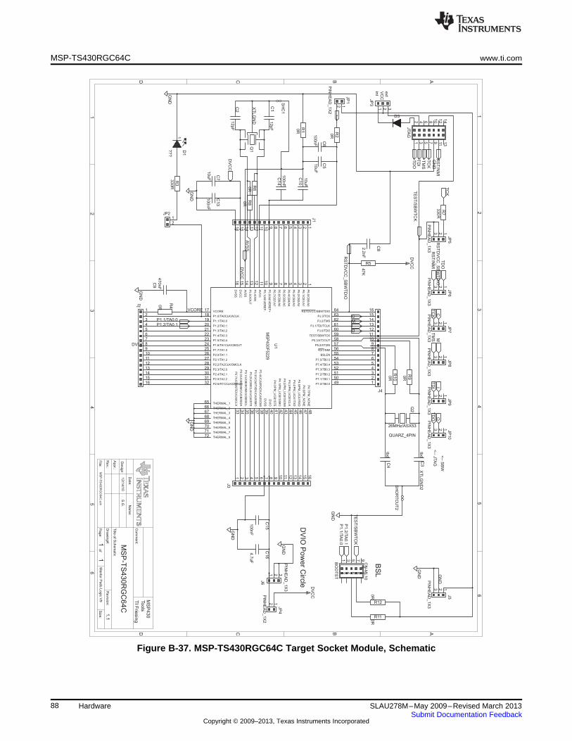
1.1
MS
P-T
S4
30
RG
C6
4C
TI F
riesin
g
Tools
MS
P4
30
11
12
/14
/10
S.G
.
65
43
21
ABCD
ABCD
De
sig
n:
Ap
pr.:
Re
v.:
Co
mm
en
t:
Dra
win
g#
:R
evis
ion
:
Pa
ge
:F
ile:
Siz
e:
Title
of S
ch
em
atic
of
Me
nto
r Pa
ds L
og
ic V
9
Da
te:
Na
me
:
65
43
21
MS
P-T
S430R
GC
64C
.sch
<-- S
BW
<-- J
TA
G
ext
int
VC
C
DV
IO P
ow
er C
ircle
BS
L
1P
6.0
/CB
0/A
0
2P
6.1
/CB
1/A
1
3P
6.2
/CB
2/A
2
4P
6.3
/CB
3/A
3
5P
6.4
/CB
4/A
4
6P
6.5
/CB
5/A
5
7P
6.6
/CB
6/A
6
8P
6.7
/CB
7/A
7
9P
5.0
/A8/V
ER
EF
+
10
P5
.1/A
9/V
ER
EF
-
11
AV
CC
12
P5
.4/X
IN
13
P5.5
/XO
UT
14
AV
SS
15
DV
CC
16
DV
SS
17 VCORE
18 P1.0/TA0CLK/ACLK
19 P1.1/TA0.0
20 P1.2/TA0.1
21 P1.3/TA0.2
22 P1.4/TA0.3
23 P1.5/TA0.4
24 P1.6/TA1CLK/CBOUT
25 P1.7/TA1.0
26 P2.0/TA1.1
27 P2.1/TA1.2
28 P2.2/TA2CLK/SMCLK
29 P2.3/TA2.0
30 P2.4/TA2.1
31 P2.5/TA2.2
32 P2.6/RTCCLK/DMAE0
33
P2
.7/U
CB
0S
TE
/UC
A0C
LK
34
P3.0
/UC
B0S
IMO
/UC
B0S
DA
35
P3
.1/U
CB
0S
OM
I/UC
B0
SC
L
36
P3
.2/U
CB
0C
LK
/UC
A0S
TE
37
P3.3
/UC
A0T
XD
/UC
A0S
IMO
38
P3.4
/UC
A0R
XD
/UC
A0
SO
MI
39
DV
SS
40
DV
IO
41
P4
.0/P
M_U
CB
1S
TE
42
P4.1
/PM
_U
CB
1S
IMO
43
P4.2
/PM
_U
CB
1S
OM
I
44
P4.3
/PM
_U
CB
1C
LK
45
P4.4
/PM
_U
CA
1T
XD
46
P4
.5/P
M_U
CA
1R
XD
47
P4.6
/PM
_N
ON
E
48
P4.7
/PM
_N
ON
E
49P7.0/TB0.0
50P7.1/TB0.1
51P7.2/TB0.2
52P7.3/TB0.3
53P7.4/TB0.4
54P7.5/TB0.5
55BSLEN
56RST/NMI
57P5.2/XT2IN
58P5.3/XT2OUT
59TEST/SBWTCK
60PJ.0/TDO
61PJ.1/TDI/TCLK
62PJ.2/TMS
63PJ.3/TCK
64RSTDVCC/SBWTDIO
65 THERMAL_1
66 THERMAL_2
67 THERMAL_3
68 THERMAL_4
69 THERMAL_5
70 THERMAL_6
71 THERMAL_7
72 THERMAL_8
U1
MS
P430F
5229
12
34
56
78
910
11
12
13
14
JTA
G
12
34
56
78
91
0
BO
OT
ST
CN
-ML10
12345678910
11
12
13
14
15
16
J1
123
45
678
91011
1213
141516
J2
1 2 3 4 5 6 7 8 910
11
12
13
14
15
16
J3
123
45
678
91011
1213
141516
J4
123
JP
5
PIN
HE
AD
_1X
3
123
JP
6
PIN
HE
AD
_1X
3
123
JP
7
PIN
HE
AD
_1X
3
123
JP
8
PIN
HE
AD
_1X
3
123
JP
9
PIN
HE
AD
_1X
3
123 JP
10
PIN
HE
AD
_1X
3
123
J5
PIN
HE
AD
_1X
3
R7
330R
1 2 3
JP
3
C1
0
10uF
C1
4100nF
C5
10uF
C6
100nF
R10R R
20R
R60R
R80R
C1
12pF
C2
12pF
C7
10uF
C1
3
100nF
12
JP2
R3
330R
12
D1
??
?R
40R
C9
470nF
R5
47K
C82.2
nF
R110R
R12
0R
C1
6
4.7
uF
C3
tbd
C4
tbd
R90R
R1
00R
C1
5
100nF
1 2 3
J6
PIN
HE
AD
_1X
3
12
JP
4
PIN
HE
AD
_1X
2
D3
Q2
QUARZ_4PIN
26MHz/ASX53
Q1
12
JP
1
PIN
HE
AD
_1X
2
SH
C1
SH
OR
TC
UT
2
GN
D
GN
D
GN
D
GN
D
XT
LG
ND
VCORE
GN
D
GN
D
DV
CCD
VC
C
GN
D
XT
LG
ND
2
GN
D
GN
D
DV
CC
GN
D
RS
T/N
MI
TC
K
TM
ST
DI
TD
O
RS
TD
VC
C_
SB
WT
DIO
TD
O
RS
T/N
MI
TC
K
CT
CK
MT
MS
IT
DI
OT
DO
DV
CC
P1
.2/T
A0
.1P
1.1
/TA
0.0
TE
ST
/SB
WT
CK
CMIO
DVCC
P1.1/TA0.0P1.2/TA0.1
RS
TD
VC
C_
SB
WT
DIO
TE
ST
/SB
WT
CK
AV
SS
MSP-TS430RGC64C www.ti.com
Figure B-37. MSP-TS430RGC64C Target Socket Module, Schematic
88 Hardware SLAU278M–May 2009–Revised March 2013Submit Documentation Feedback
Copyright © 2009–2013, Texas Instruments Incorporated
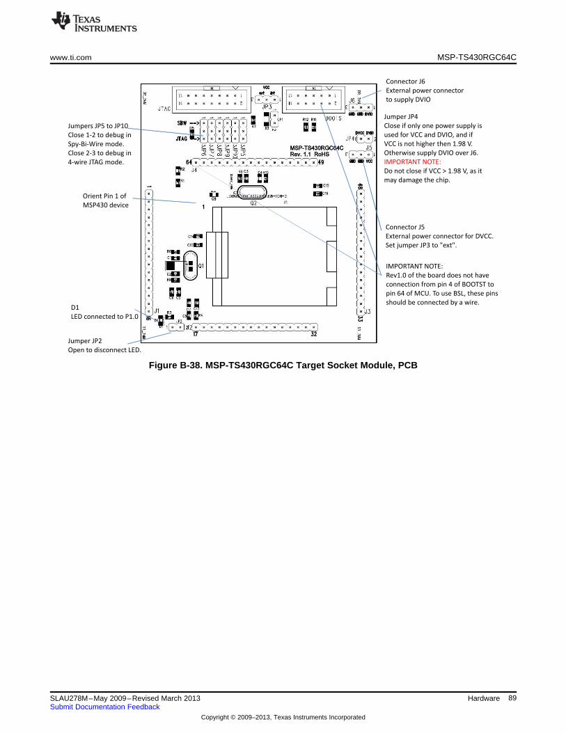
Connector J5
External power connector for DVCC.
Set jumper JP3 to "ext".
IMPORTANT NOTE:
Rev1.0 of the board does not have
connection from pin 4 of BOOTST to
pin 64 of MCU. To use BSL, these pins
should be connected by a wire.
Jumper JP2
Open to disconnect LED.
D1
LED connected to P1.0
Orient Pin 1 of
MSP430 device
Jumpers JP5 to JP10
-2 to debug in
Spy-Bi-Wire mode.
Close 2-3 to debug in
4-wire JTAG mode.
Close 1
Jumper JP4
Close if only one power supply is
used for VCC and DVIO, and if
VCC is not higher then 1.98 V.
Otherwise supply DVIO over J6.
Do not close if VCC > 1.98 V, as it
may damage the chip.
IMPORTANT NOTE:
Connector J6
External power connector
to supply DVIO
www.ti.com MSP-TS430RGC64C
Figure B-38. MSP-TS430RGC64C Target Socket Module, PCB
89SLAU278M–May 2009–Revised March 2013 HardwareSubmit Documentation Feedback
Copyright © 2009–2013, Texas Instruments Incorporated
MSP-TS430RGC64C www.ti.com
Table B-21. MSP-TS430RGC64C Bill of Materials
Item Qty Reference Value Description Comment Supplier No.
1 0 C1, C2 12pF CAP, SMD, Ceramic, 0805 DNP C1 C2
2 0 C3, C4 tbd CAP, SMD, Ceramic, 0805 DNP C3 C4
4 3 C5, C7, C10 10uF CAP, SMD, Ceramic, 0805
5 5 C8 C6 C13-15 100nF CAP, SMD, Ceramic, 0805 DigiKey: 311-1245-2-ND
5 5 C8 2.2nF CAP, SMD, Ceramic, 0805
6 1 C9 470nF CAP, SMD, Ceramic, 0805 DigiKey: 478-1403-2-ND
7 1 C16 4.7uF CAP, SMD, Ceramic, 0805
8 1 D1 Green LED LED, SMD, 0805
DNP: headers andreceptacles enclosed with
Pin header 1x16: Grid: 100mil kit. Keep vias free of9 4 J1-J4 16-pin header (2.54 mm) solder.: Header SAM1029-16-ND: Receptacle SAM1213-16-ND
Pin header 1x3: Grid: 100mil10 2 J5, J6 3-pin header, male, TH SAM1035-03-ND(2.54 mm)
JP5, JP6, JP7, Pinheader 1x3: Grid: 100mil11 3-pin header, male, TH place jumpers on pins 2-3 SAM1035-03-NDJP8, JP9, JP10 (2.54 mm)
Pin header 1x3: Grid: 100mil12 JP3 3-pin header, male, TH place jumper on pins 1-2 SAM1035-03-ND(2.54 mm)
Pin header 1x2; Grid: 100mil13 JP1, JP2, JP4 2-pin header, male, TH place jumper on header SAM1035-02-ND(2.54 mm)
Place on: JP1, JP2, JP3,14 10 Jumper JP4, JP5, JP6, JP7, JP8, 15-38-1024-ND
JP9, JP10
Header, THD, Male 2x7 Pin,15 1 JTAG 2x7Pin,Wanne HRP14H-NDWanne, 100mil spacing
Header, THD, Male 2x5 Pin,16 0 BOOTST 2x5Pin,Wanne DNPWanne, 100mil spacing
CRYSTAL, SMD, 5x3MM,17 1 Q1 26MHz/ASX53 Only Kit.26MHz
CRYSTAL, SMD, 5x3MM,18 0 Q2 26MHz/ASX53 300-8219-1-ND26MHz
DIODE, SMD, SOD123,19 1 D3 LL103A Buerklin: 24S3406Schottky
20 2 R3, R7 330 Ohm, SMD0805 541-330ATR-ND
21 1 R5 47k Ohm, SMD0805 RES, SMD, 0805, 1/8W, x% 541-47000ATR-ND
R1, R2, R4, DNP: R6, R8, R9, R10,22 R6, R8, R9, 0 Ohm, SMD0805 RES, SMD, 0805, 1/8W, x% 541-000ATR-NDR11,R12R10, R11, R12
Socket: QFN11T064-006-N-23 1 U1 Manuf.: YamaichiHSP
IC, MCU, SMD, 9.15x9.15mm24 2 MSP430 MSP430F5229IRGCR Thermal Pad with Socket
Rubber stand apply to corners at bottom25 4 Rubber stand off Buerklin: 20H1724off side
26 1 PCB 84 x 76 mm 84 x 76 mm
90 Hardware SLAU278M–May 2009–Revised March 2013Submit Documentation Feedback
Copyright © 2009–2013, Texas Instruments Incorporated
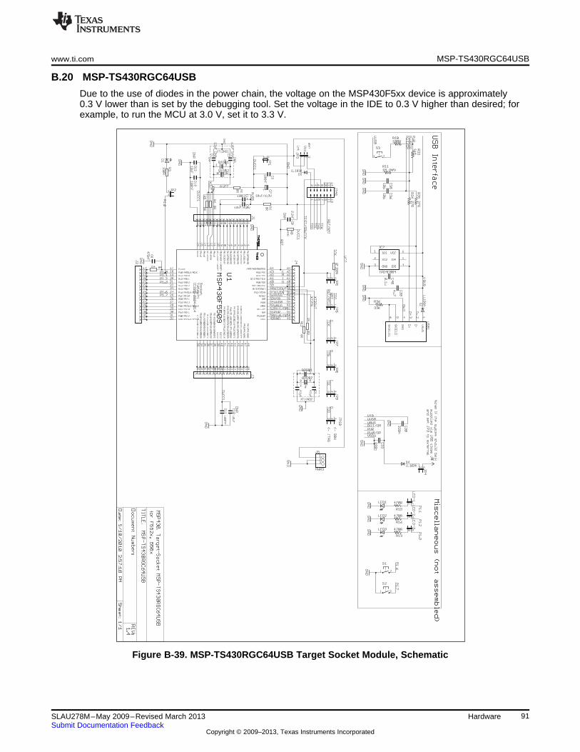
www.ti.com MSP-TS430RGC64USB
B.20 MSP-TS430RGC64USB
Due to the use of diodes in the power chain, the voltage on the MSP430F5xx device is approximately0.3 V lower than is set by the debugging tool. Set the voltage in the IDE to 0.3 V higher than desired; forexample, to run the MCU at 3.0 V, set it to 3.3 V.
Figure B-39. MSP-TS430RGC64USB Target Socket Module, Schematic
91SLAU278M–May 2009–Revised March 2013 HardwareSubmit Documentation Feedback
Copyright © 2009–2013, Texas Instruments Incorporated
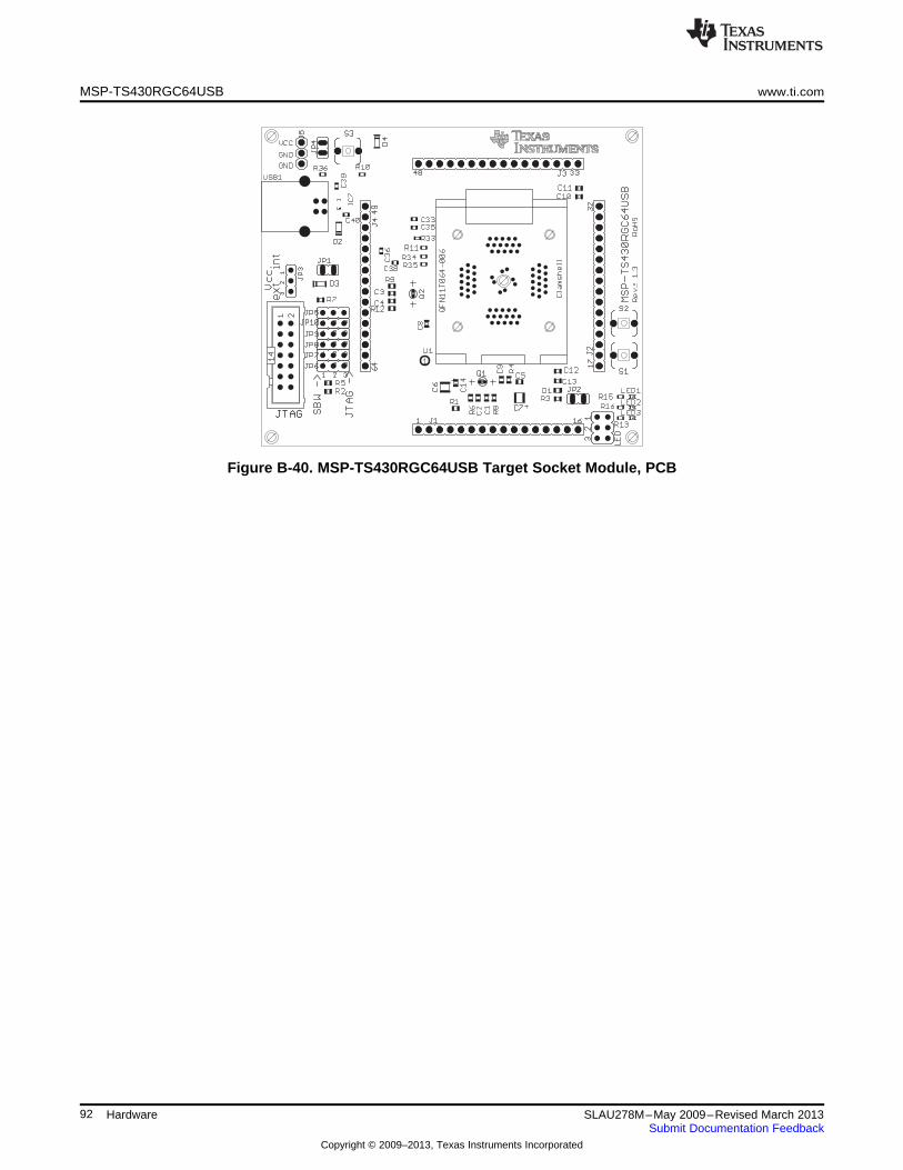
MSP-TS430RGC64USB www.ti.com
Figure B-40. MSP-TS430RGC64USB Target Socket Module, PCB
92 Hardware SLAU278M–May 2009–Revised March 2013Submit Documentation Feedback
Copyright © 2009–2013, Texas Instruments Incorporated
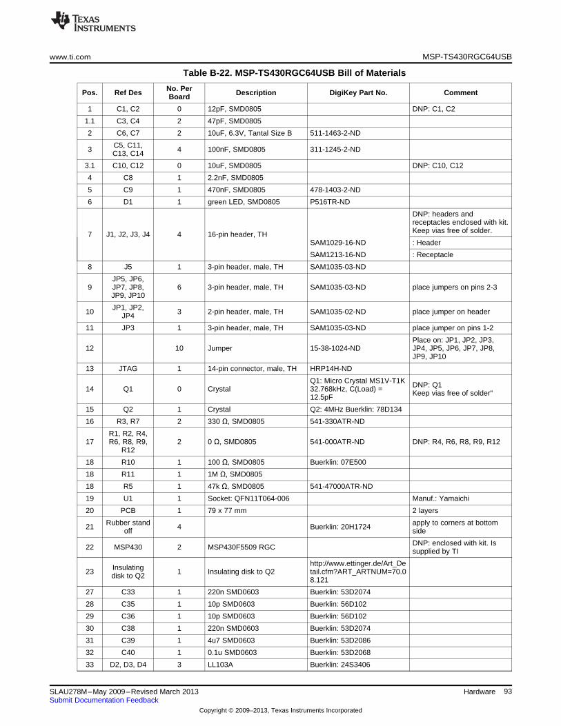
www.ti.com MSP-TS430RGC64USB
Table B-22. MSP-TS430RGC64USB Bill of Materials
No. PerPos. Ref Des Description DigiKey Part No. CommentBoard
1 C1, C2 0 12pF, SMD0805 DNP: C1, C2
1.1 C3, C4 2 47pF, SMD0805
2 C6, C7 2 10uF, 6.3V, Tantal Size B 511-1463-2-ND
C5, C11,3 4 100nF, SMD0805 311-1245-2-NDC13, C14
3.1 C10, C12 0 10uF, SMD0805 DNP: C10, C12
4 C8 1 2.2nF, SMD0805
5 C9 1 470nF, SMD0805 478-1403-2-ND
6 D1 1 green LED, SMD0805 P516TR-ND
DNP: headers andreceptacles enclosed with kit.Keep vias free of solder.7 J1, J2, J3, J4 4 16-pin header, TH
SAM1029-16-ND : Header
SAM1213-16-ND : Receptacle
8 J5 1 3-pin header, male, TH SAM1035-03-ND
JP5, JP6,9 JP7, JP8, 6 3-pin header, male, TH SAM1035-03-ND place jumpers on pins 2-3
JP9, JP10
JP1, JP2,10 3 2-pin header, male, TH SAM1035-02-ND place jumper on headerJP4
11 JP3 1 3-pin header, male, TH SAM1035-03-ND place jumper on pins 1-2
Place on: JP1, JP2, JP3,12 10 Jumper 15-38-1024-ND JP4, JP5, JP6, JP7, JP8,
JP9, JP10
13 JTAG 1 14-pin connector, male, TH HRP14H-ND
Q1: Micro Crystal MS1V-T1K DNP: Q114 Q1 0 Crystal 32.768kHz, C(Load) = Keep vias free of solder"12.5pF
15 Q2 1 Crystal Q2: 4MHz Buerklin: 78D134
16 R3, R7 2 330 Ω, SMD0805 541-330ATR-ND
R1, R2, R4,17 R6, R8, R9, 2 0 Ω, SMD0805 541-000ATR-ND DNP: R4, R6, R8, R9, R12
R12
18 R10 1 100 Ω, SMD0805 Buerklin: 07E500
18 R11 1 1M Ω, SMD0805
18 R5 1 47k Ω, SMD0805 541-47000ATR-ND
19 U1 1 Socket: QFN11T064-006 Manuf.: Yamaichi
20 PCB 1 79 x 77 mm 2 layers
Rubber stand apply to corners at bottom21 4 Buerklin: 20H1724off side
DNP: enclosed with kit. Is22 MSP430 2 MSP430F5509 RGC supplied by TI
http://www.ettinger.de/Art_DeInsulating23 1 Insulating disk to Q2 tail.cfm?ART_ARTNUM=70.0disk to Q2 8.121
27 C33 1 220n SMD0603 Buerklin: 53D2074
28 C35 1 10p SMD0603 Buerklin: 56D102
29 C36 1 10p SMD0603 Buerklin: 56D102
30 C38 1 220n SMD0603 Buerklin: 53D2074
31 C39 1 4u7 SMD0603 Buerklin: 53D2086
32 C40 1 0.1u SMD0603 Buerklin: 53D2068
33 D2, D3, D4 3 LL103A Buerklin: 24S3406
93SLAU278M–May 2009–Revised March 2013 HardwareSubmit Documentation Feedback
Copyright © 2009–2013, Texas Instruments Incorporated
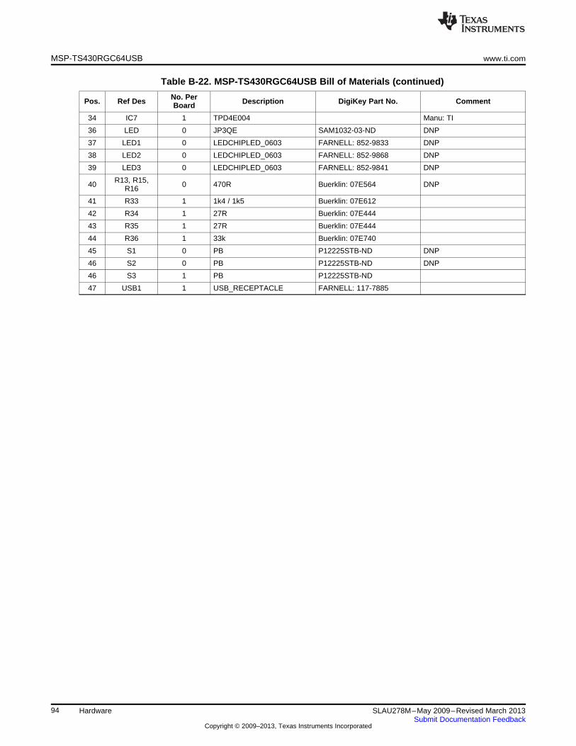
MSP-TS430RGC64USB www.ti.com
Table B-22. MSP-TS430RGC64USB Bill of Materials (continued)
No. PerPos. Ref Des Description DigiKey Part No. CommentBoard
34 IC7 1 TPD4E004 Manu: TI
36 LED 0 JP3QE SAM1032-03-ND DNP
37 LED1 0 LEDCHIPLED_0603 FARNELL: 852-9833 DNP
38 LED2 0 LEDCHIPLED_0603 FARNELL: 852-9868 DNP
39 LED3 0 LEDCHIPLED_0603 FARNELL: 852-9841 DNP
R13, R15,40 0 470R Buerklin: 07E564 DNPR16
41 R33 1 1k4 / 1k5 Buerklin: 07E612
42 R34 1 27R Buerklin: 07E444
43 R35 1 27R Buerklin: 07E444
44 R36 1 33k Buerklin: 07E740
45 S1 0 PB P12225STB-ND DNP
46 S2 0 PB P12225STB-ND DNP
46 S3 1 PB P12225STB-ND
47 USB1 1 USB_RECEPTACLE FARNELL: 117-7885
94 Hardware SLAU278M–May 2009–Revised March 2013Submit Documentation Feedback
Copyright © 2009–2013, Texas Instruments Incorporated
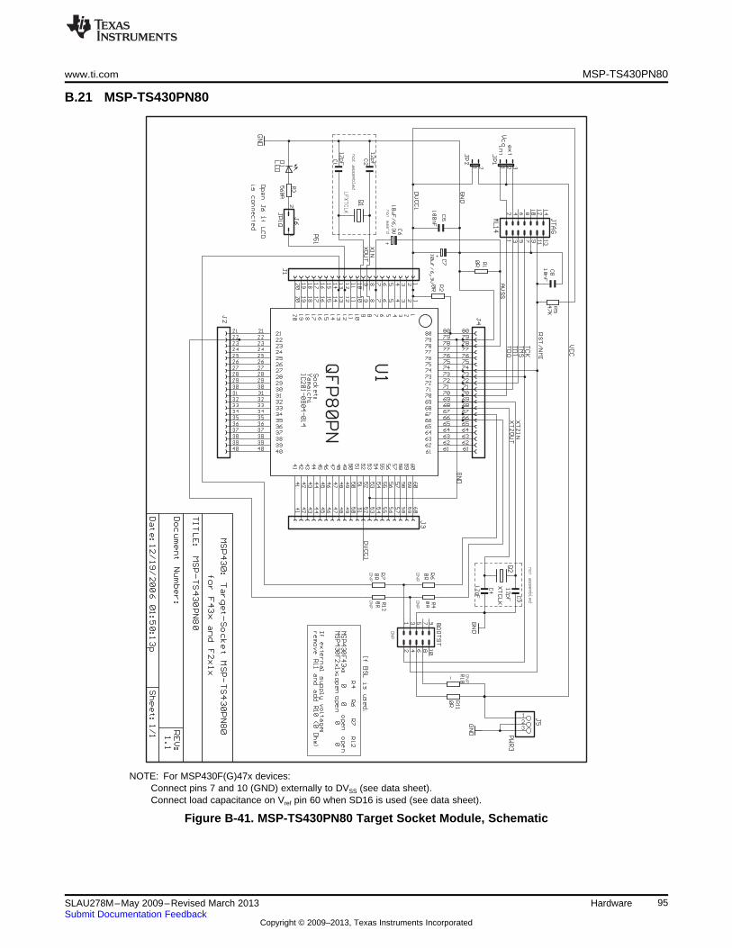
www.ti.com MSP-TS430PN80
B.21 MSP-TS430PN80
NOTE: For MSP430F(G)47x devices:Connect pins 7 and 10 (GND) externally to DVSS (see data sheet).Connect load capacitance on Vref pin 60 when SD16 is used (see data sheet).
Figure B-41. MSP-TS430PN80 Target Socket Module, Schematic
95SLAU278M–May 2009–Revised March 2013 HardwareSubmit Documentation Feedback
Copyright © 2009–2013, Texas Instruments Incorporated
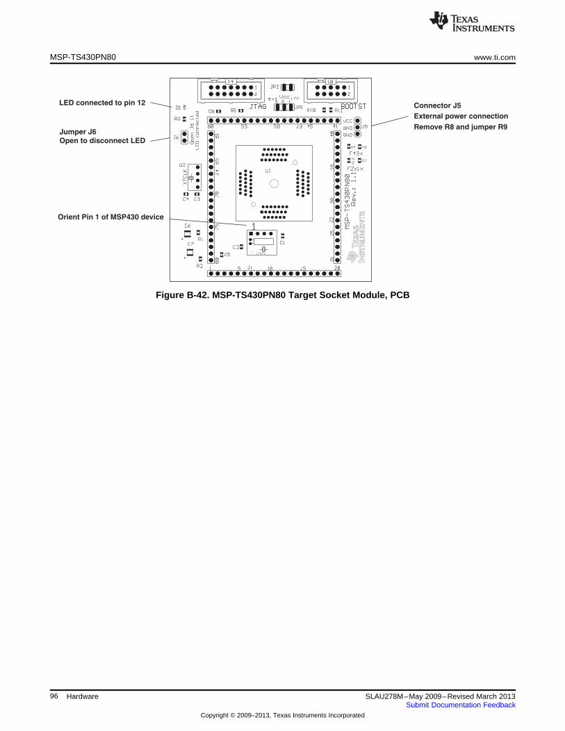
Connector J5
External power connection
Remove R8 and jumper R9
LED connected to pin 12
Jumper J6
Open to disconnect LED
Orient Pin 1 of MSP430 device
MSP-TS430PN80 www.ti.com
Figure B-42. MSP-TS430PN80 Target Socket Module, PCB
96 Hardware SLAU278M–May 2009–Revised March 2013Submit Documentation Feedback
Copyright © 2009–2013, Texas Instruments Incorporated
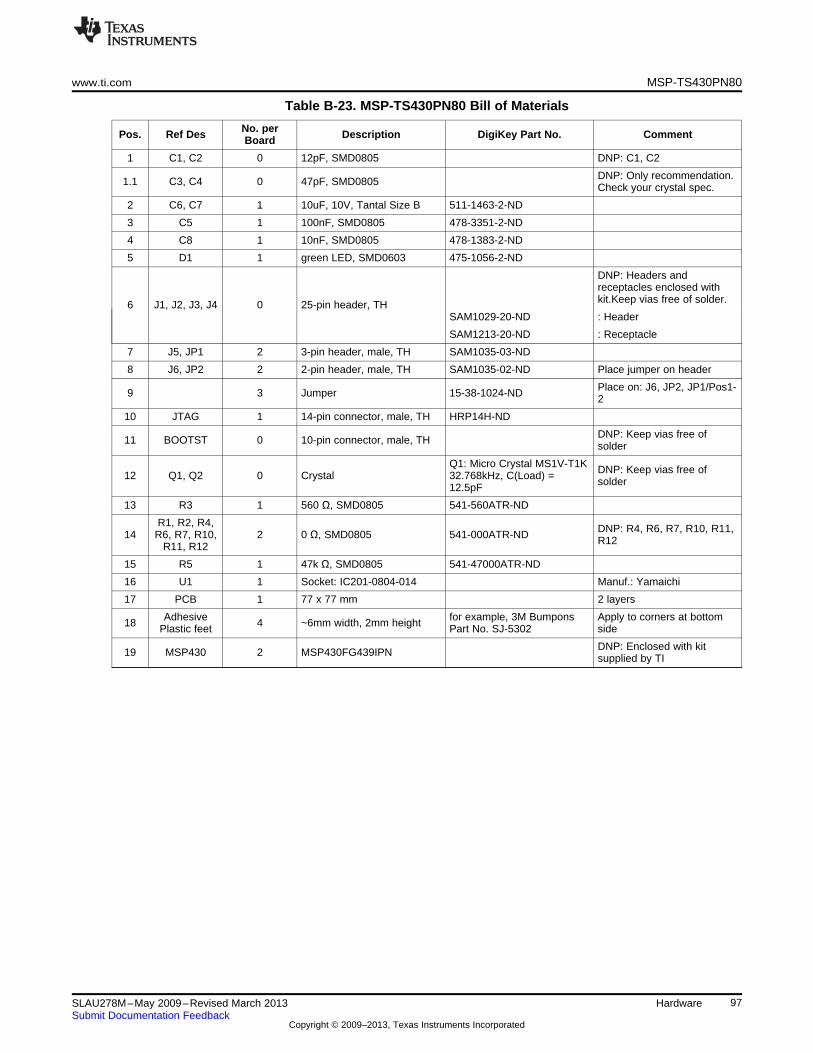
www.ti.com MSP-TS430PN80
Table B-23. MSP-TS430PN80 Bill of Materials
No. perPos. Ref Des Description DigiKey Part No. CommentBoard
1 C1, C2 0 12pF, SMD0805 DNP: C1, C2
DNP: Only recommendation.1.1 C3, C4 0 47pF, SMD0805 Check your crystal spec.
2 C6, C7 1 10uF, 10V, Tantal Size B 511-1463-2-ND
3 C5 1 100nF, SMD0805 478-3351-2-ND
4 C8 1 10nF, SMD0805 478-1383-2-ND
5 D1 1 green LED, SMD0603 475-1056-2-ND
DNP: Headers andreceptacles enclosed withkit.Keep vias free of solder.6 J1, J2, J3, J4 0 25-pin header, TH
SAM1029-20-ND : Header
SAM1213-20-ND : Receptacle
7 J5, JP1 2 3-pin header, male, TH SAM1035-03-ND
8 J6, JP2 2 2-pin header, male, TH SAM1035-02-ND Place jumper on header
Place on: J6, JP2, JP1/Pos1-9 3 Jumper 15-38-1024-ND 2
10 JTAG 1 14-pin connector, male, TH HRP14H-ND
DNP: Keep vias free of11 BOOTST 0 10-pin connector, male, TH solder
Q1: Micro Crystal MS1V-T1K DNP: Keep vias free of12 Q1, Q2 0 Crystal 32.768kHz, C(Load) = solder12.5pF
13 R3 1 560 Ω, SMD0805 541-560ATR-ND
R1, R2, R4, DNP: R4, R6, R7, R10, R11,14 R6, R7, R10, 2 0 Ω, SMD0805 541-000ATR-ND R12R11, R12
15 R5 1 47k Ω, SMD0805 541-47000ATR-ND
16 U1 1 Socket: IC201-0804-014 Manuf.: Yamaichi
17 PCB 1 77 x 77 mm 2 layers
Adhesive for example, 3M Bumpons Apply to corners at bottom18 4 ~6mm width, 2mm heightPlastic feet Part No. SJ-5302 side
DNP: Enclosed with kit19 MSP430 2 MSP430FG439IPN supplied by TI
97SLAU278M–May 2009–Revised March 2013 HardwareSubmit Documentation Feedback
Copyright © 2009–2013, Texas Instruments Incorporated
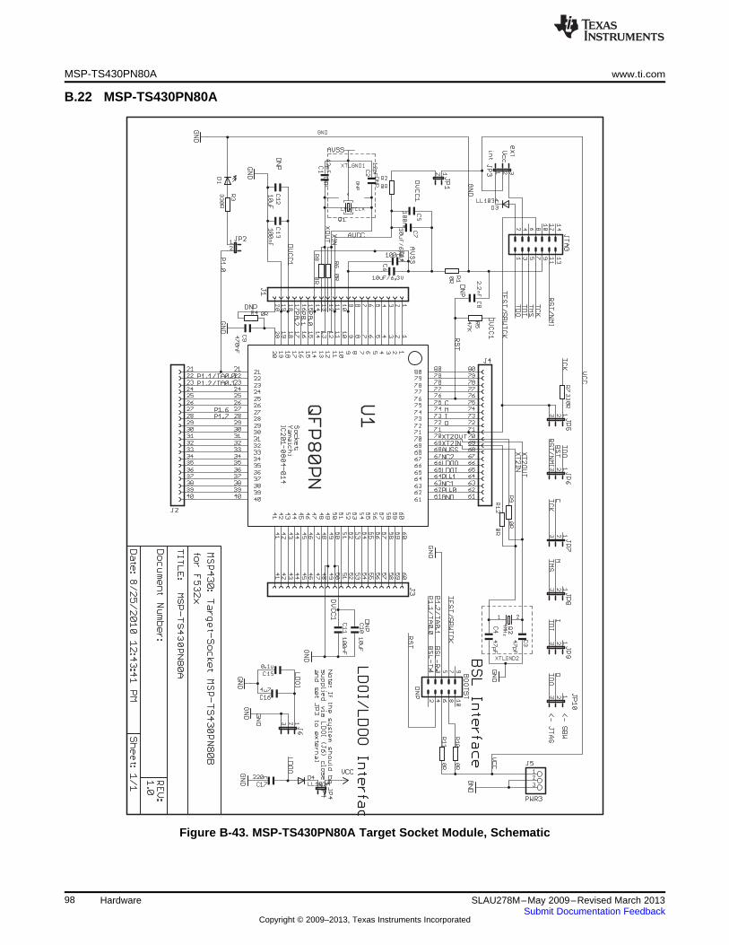
MSP-TS430PN80A www.ti.com
B.22 MSP-TS430PN80A
Figure B-43. MSP-TS430PN80A Target Socket Module, Schematic
98 Hardware SLAU278M–May 2009–Revised March 2013Submit Documentation Feedback
Copyright © 2009–2013, Texas Instruments Incorporated
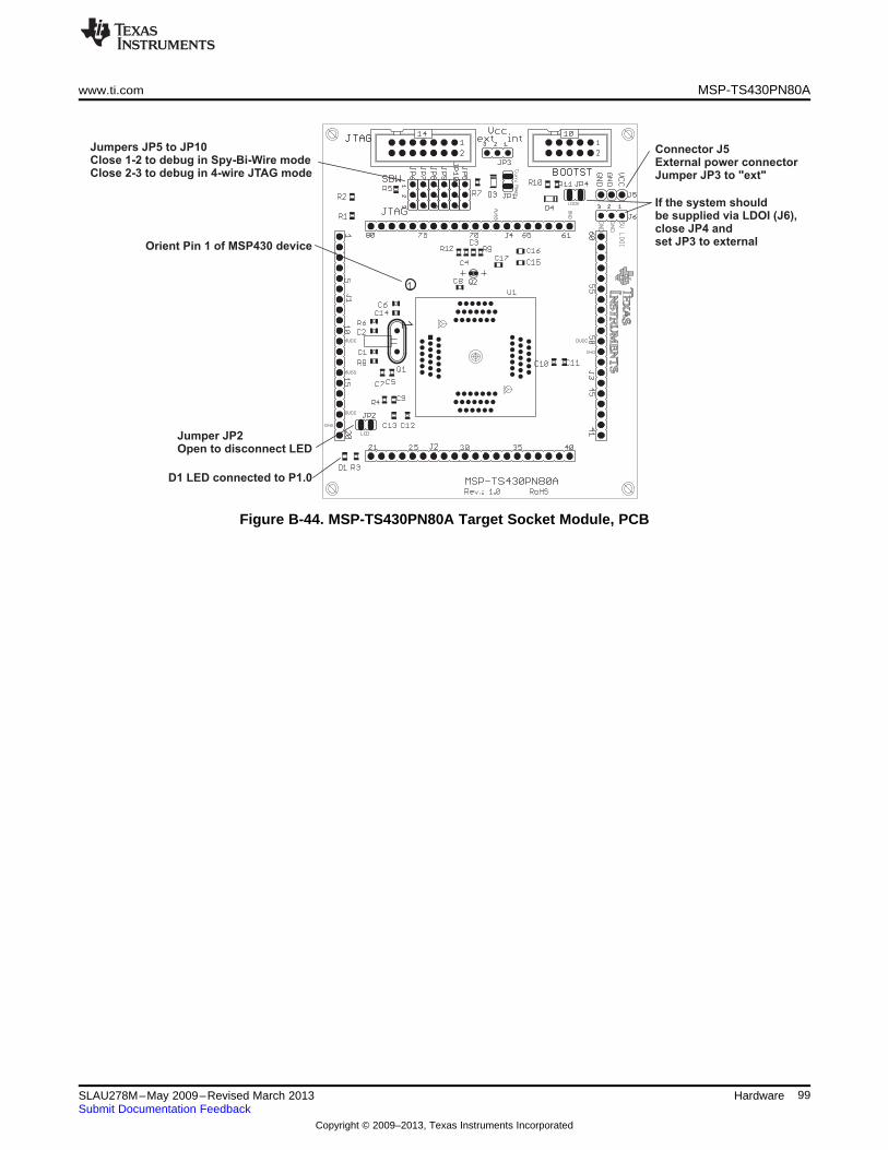
Connector J5External power connectorJumper JP3 to "ext"
Orient Pin 1 of MSP430 device
Jumpers JP5 to JP10Close 1-2 to debug in Spy-Bi-Wire modeClose 2-3 to debug in 4-wire JTAG mode
D1 LED connected to P1.0
Jumper JP2Open to disconnect LED
If the system shouldbe supplied via LDOI (J6),close JP4 andset JP3 to external
www.ti.com MSP-TS430PN80A
Figure B-44. MSP-TS430PN80A Target Socket Module, PCB
99SLAU278M–May 2009–Revised March 2013 HardwareSubmit Documentation Feedback
Copyright © 2009–2013, Texas Instruments Incorporated
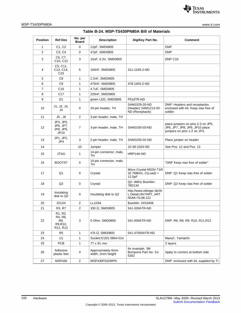
MSP-TS430PN80A www.ti.com
Table B-24. MSP-TS430PN80A Bill of Materials
No. perPosition Ref Des Description DigiKey Part No. CommentBoard
1 C1, C2 0 12pF, SMD0805 DNP
2 C3, C4 0 47pF, SMD0805 DNP
C6, C7,3 3 10uF, 6.3V, SMD0805 DNP C10C10, C12
C5, C11,4 C13, C14, 5 100nF, SMD0805 311-1245-2-ND
C15
5 C8 1 2.2nF, SMD0805
6 C9 1 470nF, SMD0805 478-1403-2-ND
7 C16 1 4.7uF, SMD0805
8 C17 1 220nF, SMD0805
9 D1 1 green LED, SMD0805 P516TR-ND
SAM1029-20-ND DNP: Headers and receptaclesJ1, J2, J3,10 0 20-pin header, TH (Header) SAM1213-20- enclosed with kit. Keep vias free ofJ4 ND (Receptacle) solder:
11 J5 , J6 2 3-pin header, male, TH
JP3, JP5, place jumpers on pins 2-3 on JP5,JP6, JP7,12 7 3-pin header, male, TH SAM1035-03-ND JP6, JP7, JP8, JP9, JP10 placeJP8, JP9, jumpers on pins 1-2 on JP3,JP10
JP1, JP2,13 3 2-pin header, male, TH SAM1035-02-ND Place jumper on headerJP4
14 10 Jumper 15-38-1024-ND See Pos. 12 and Pos. 13
14-pin connector, male,15 JTAG 1 HRP14H-NDTH
10-pin connector, male,16 BOOTST 0 "DNP Keep vias free of solder"TH
Micro Crystal MS3V-T1R17 Q1 0 Crystal 32.768kHz, C(Load) = DNP: Q1 Keep vias free of solder
12.5pF
Q2: 4MHz Buerklin:18 Q2 0 Crystal DNP: Q2 Keep vias free of solder78D134
http://www.ettinger.de/ArInsulating19 0 Insulating disk to Q2 t_Detail.cfm?ART_ARTdisk to Q2 NUM=70.08.121
20 D3,D4 2 LL103A Buerklin: 24S3406
21 R3, R7 2 330 Ω, SMD0805 541-330ATR-ND
R1, R2,R4, R6,
22 R8, 3 0 Ohm, SMD0805 541-000ATR-ND DNP: R6, R8, R9, R10, R11,R12R9,R10,
R11, R12
23 R5 1 47k Ω, SMD0805 541-47000ATR-ND
24 U1 1 Socket:IC201-0804-014 Manuf.: Yamaichi
25 PCB 1 77 x 91 mm 2 layers
for example, 3MAdhesive Approximately 6mm26 4 Bumpons Part No. SJ- Apply to corners at bottom sideplastic feet width, 2mm height 5302
27 MSP430 2 MSP430F5329IPN DNP: enclosed with kit, supplied by TI
100 Hardware SLAU278M–May 2009–Revised March 2013Submit Documentation Feedback
Copyright © 2009–2013, Texas Instruments Incorporated
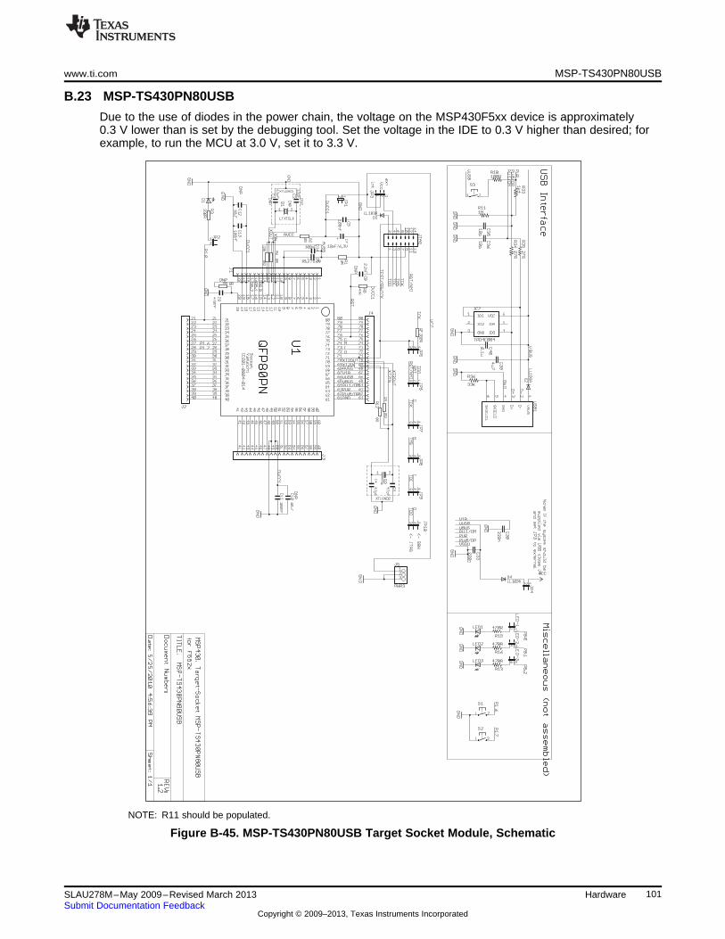
www.ti.com MSP-TS430PN80USB
B.23 MSP-TS430PN80USB
Due to the use of diodes in the power chain, the voltage on the MSP430F5xx device is approximately0.3 V lower than is set by the debugging tool. Set the voltage in the IDE to 0.3 V higher than desired; forexample, to run the MCU at 3.0 V, set it to 3.3 V.
NOTE: R11 should be populated.
Figure B-45. MSP-TS430PN80USB Target Socket Module, Schematic
101SLAU278M–May 2009–Revised March 2013 HardwareSubmit Documentation Feedback
Copyright © 2009–2013, Texas Instruments Incorporated
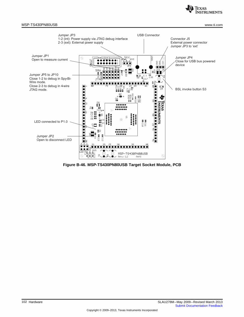
Jumper JP31-2 (int): Power supply via JTAG debug interface2-3 (ext): External power supply
Connector J5External power connectorJumper JP3 to ‘ext’
USB Connector
BSL invoke button S3
Jumper JP4Close for USB bus powereddevice
Jumper JP2Open to disconnect LED
LED connected to P1.0
Jumper JP1Open to measure current
Jumper JP5 to JP10
Close 1-2 to debug in Spy-Bi-Wire mode.
Close 2-3 to debug in 4-wireJTAG mode.
MSP-TS430PN80USB www.ti.com
Figure B-46. MSP-TS430PN80USB Target Socket Module, PCB
102 Hardware SLAU278M–May 2009–Revised March 2013Submit Documentation Feedback
Copyright © 2009–2013, Texas Instruments Incorporated
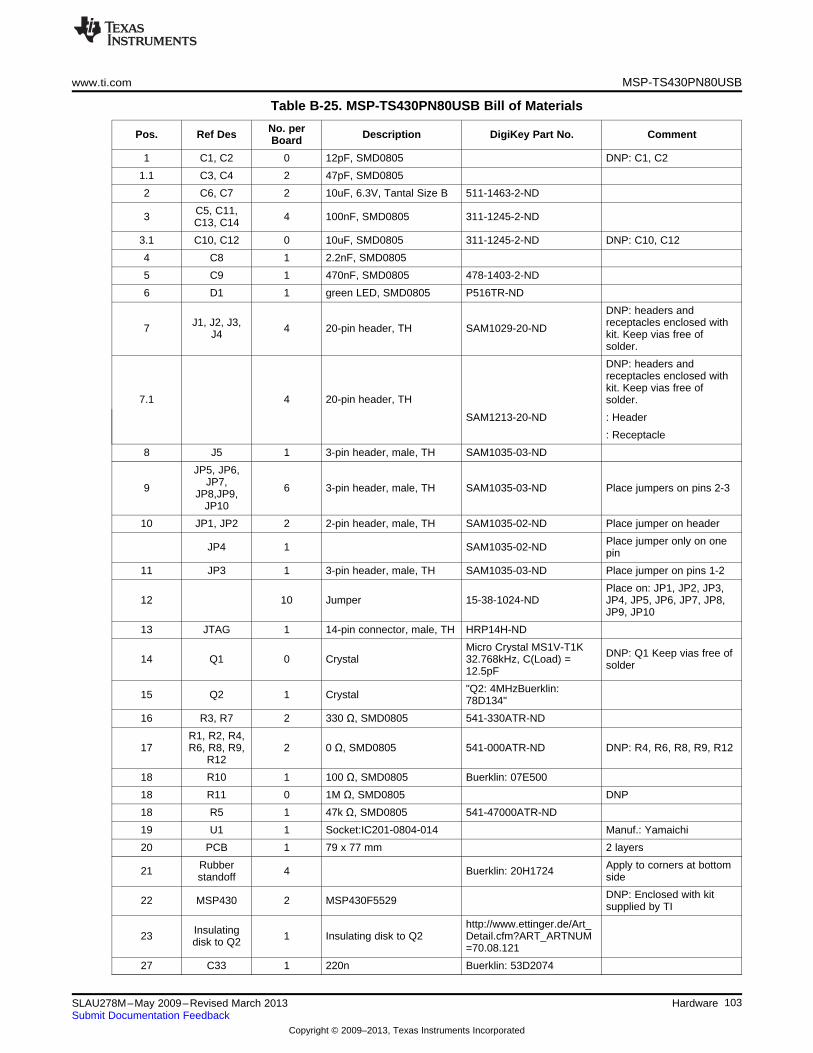
www.ti.com MSP-TS430PN80USB
Table B-25. MSP-TS430PN80USB Bill of Materials
No. perPos. Ref Des Description DigiKey Part No. CommentBoard
1 C1, C2 0 12pF, SMD0805 DNP: C1, C2
1.1 C3, C4 2 47pF, SMD0805
2 C6, C7 2 10uF, 6.3V, Tantal Size B 511-1463-2-ND
C5, C11,3 4 100nF, SMD0805 311-1245-2-NDC13, C14
3.1 C10, C12 0 10uF, SMD0805 311-1245-2-ND DNP: C10, C12
4 C8 1 2.2nF, SMD0805
5 C9 1 470nF, SMD0805 478-1403-2-ND
6 D1 1 green LED, SMD0805 P516TR-ND
DNP: headers andJ1, J2, J3, receptacles enclosed with7 4 20-pin header, TH SAM1029-20-NDJ4 kit. Keep vias free of
solder.
DNP: headers andreceptacles enclosed withkit. Keep vias free of
7.1 4 20-pin header, TH solder.
SAM1213-20-ND : Header
: Receptacle
8 J5 1 3-pin header, male, TH SAM1035-03-ND
JP5, JP6,JP7,9 6 3-pin header, male, TH SAM1035-03-ND Place jumpers on pins 2-3JP8,JP9,JP10
10 JP1, JP2 2 2-pin header, male, TH SAM1035-02-ND Place jumper on header
Place jumper only on oneJP4 1 SAM1035-02-ND pin
11 JP3 1 3-pin header, male, TH SAM1035-03-ND Place jumper on pins 1-2
Place on: JP1, JP2, JP3,12 10 Jumper 15-38-1024-ND JP4, JP5, JP6, JP7, JP8,
JP9, JP10
13 JTAG 1 14-pin connector, male, TH HRP14H-ND
Micro Crystal MS1V-T1K DNP: Q1 Keep vias free of14 Q1 0 Crystal 32.768kHz, C(Load) = solder12.5pF
"Q2: 4MHzBuerklin:15 Q2 1 Crystal 78D134"
16 R3, R7 2 330 Ω, SMD0805 541-330ATR-ND
R1, R2, R4,17 R6, R8, R9, 2 0 Ω, SMD0805 541-000ATR-ND DNP: R4, R6, R8, R9, R12
R12
18 R10 1 100 Ω, SMD0805 Buerklin: 07E500
18 R11 0 1M Ω, SMD0805 DNP
18 R5 1 47k Ω, SMD0805 541-47000ATR-ND
19 U1 1 Socket:IC201-0804-014 Manuf.: Yamaichi
20 PCB 1 79 x 77 mm 2 layers
Rubber Apply to corners at bottom21 4 Buerklin: 20H1724standoff side
DNP: Enclosed with kit22 MSP430 2 MSP430F5529 supplied by TI
http://www.ettinger.de/Art_Insulating23 1 Insulating disk to Q2 Detail.cfm?ART_ARTNUMdisk to Q2 =70.08.121
27 C33 1 220n Buerklin: 53D2074
103SLAU278M–May 2009–Revised March 2013 HardwareSubmit Documentation Feedback
Copyright © 2009–2013, Texas Instruments Incorporated
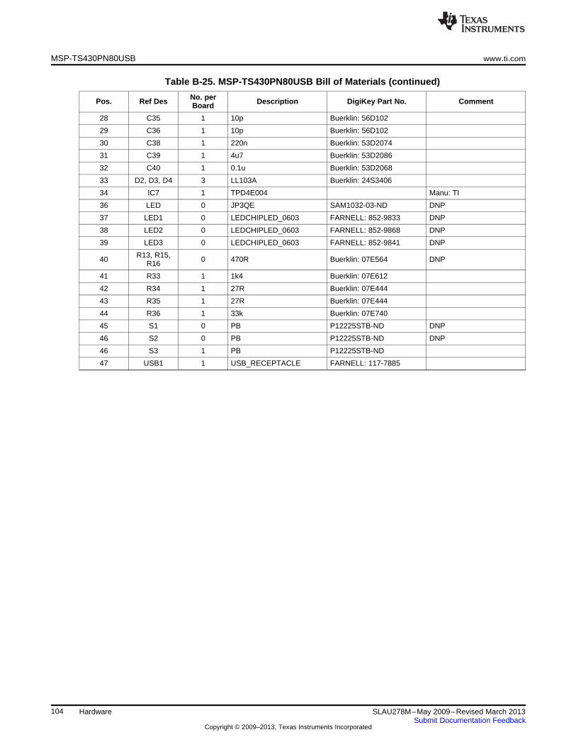
MSP-TS430PN80USB www.ti.com
Table B-25. MSP-TS430PN80USB Bill of Materials (continued)
No. perPos. Ref Des Description DigiKey Part No. CommentBoard
28 C35 1 10p Buerklin: 56D102
29 C36 1 10p Buerklin: 56D102
30 C38 1 220n Buerklin: 53D2074
31 C39 1 4u7 Buerklin: 53D2086
32 C40 1 0.1u Buerklin: 53D2068
33 D2, D3, D4 3 LL103A Buerklin: 24S3406
34 IC7 1 TPD4E004 Manu: TI
36 LED 0 JP3QE SAM1032-03-ND DNP
37 LED1 0 LEDCHIPLED_0603 FARNELL: 852-9833 DNP
38 LED2 0 LEDCHIPLED_0603 FARNELL: 852-9868 DNP
39 LED3 0 LEDCHIPLED_0603 FARNELL: 852-9841 DNP
R13, R15,40 0 470R Buerklin: 07E564 DNPR16
41 R33 1 1k4 Buerklin: 07E612
42 R34 1 27R Buerklin: 07E444
43 R35 1 27R Buerklin: 07E444
44 R36 1 33k Buerklin: 07E740
45 S1 0 PB P12225STB-ND DNP
46 S2 0 PB P12225STB-ND DNP
46 S3 1 PB P12225STB-ND
47 USB1 1 USB_RECEPTACLE FARNELL: 117-7885
104 Hardware SLAU278M–May 2009–Revised March 2013Submit Documentation Feedback
Copyright © 2009–2013, Texas Instruments Incorporated
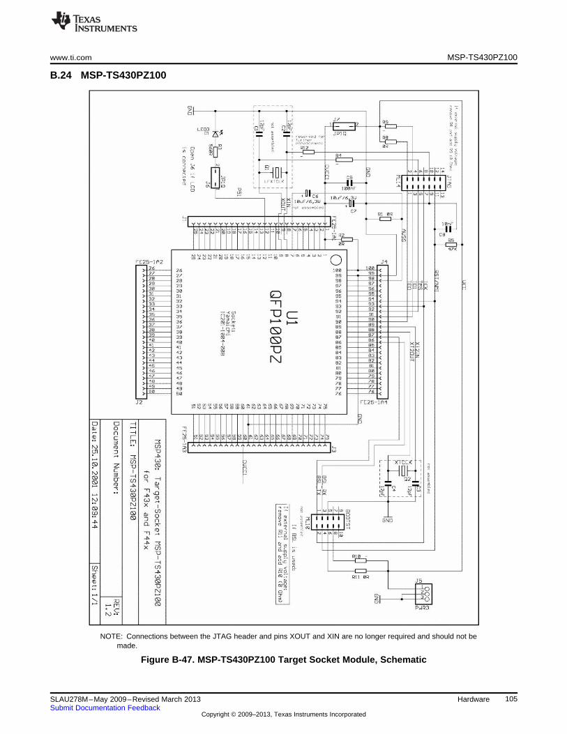
www.ti.com MSP-TS430PZ100
B.24 MSP-TS430PZ100
NOTE: Connections between the JTAG header and pins XOUT and XIN are no longer required and should not bemade.
Figure B-47. MSP-TS430PZ100 Target Socket Module, Schematic
105SLAU278M–May 2009–Revised March 2013 HardwareSubmit Documentation Feedback
Copyright © 2009–2013, Texas Instruments Incorporated
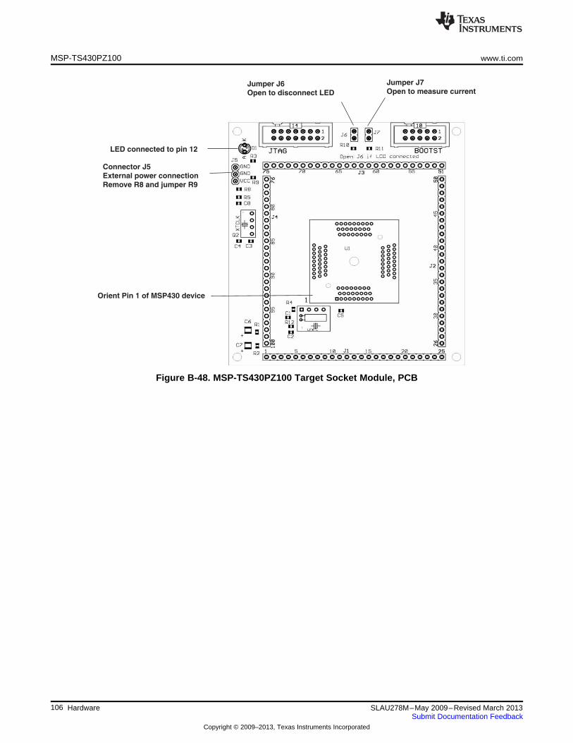
Connector J5
External power connection
Remove R8 and jumper R9
LED connected to pin 12
Jumper J6
Open to disconnect LED
Orient Pin 1 of MSP430 device
Jumper J7
Open to measure current
MSP-TS430PZ100 www.ti.com
Figure B-48. MSP-TS430PZ100 Target Socket Module, PCB
106 Hardware SLAU278M–May 2009–Revised March 2013Submit Documentation Feedback
Copyright © 2009–2013, Texas Instruments Incorporated
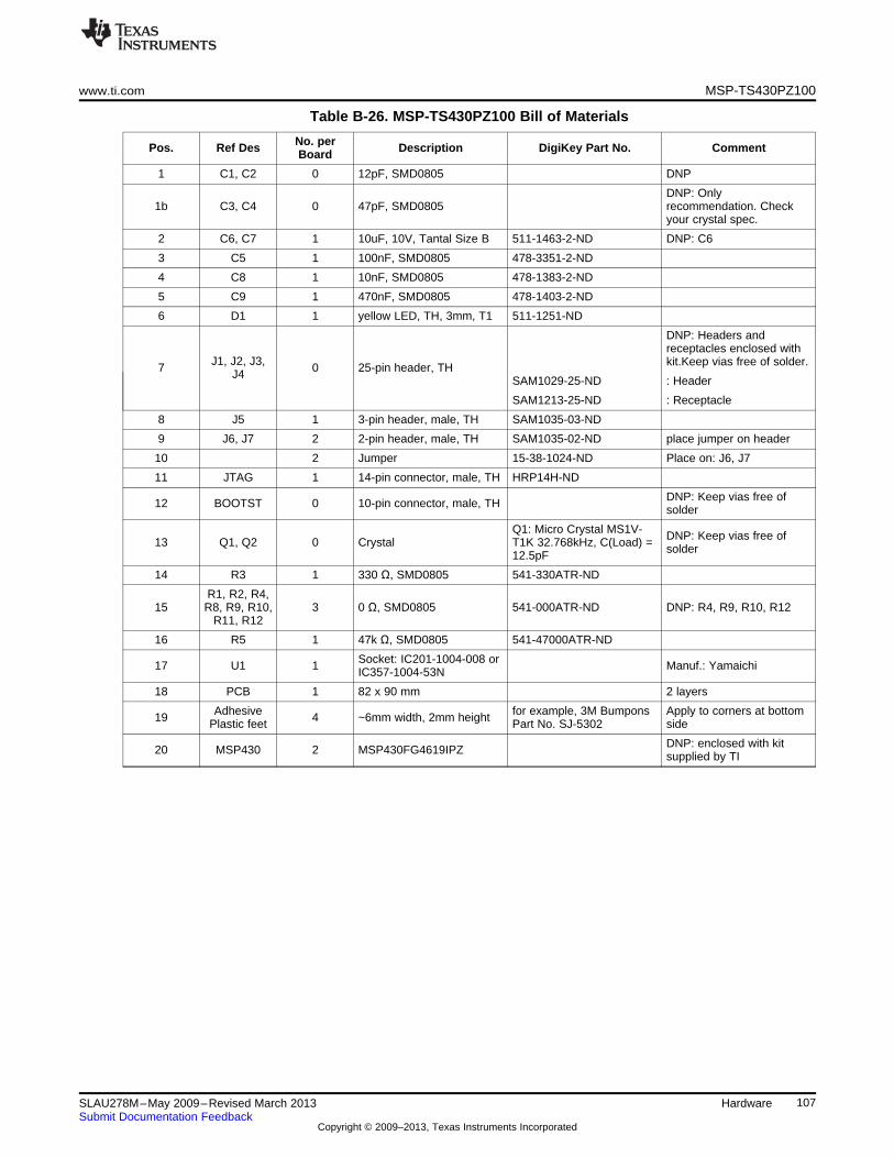
www.ti.com MSP-TS430PZ100
Table B-26. MSP-TS430PZ100 Bill of Materials
No. perPos. Ref Des Description DigiKey Part No. CommentBoard
1 C1, C2 0 12pF, SMD0805 DNP
DNP: Only1b C3, C4 0 47pF, SMD0805 recommendation. Check
your crystal spec.
2 C6, C7 1 10uF, 10V, Tantal Size B 511-1463-2-ND DNP: C6
3 C5 1 100nF, SMD0805 478-3351-2-ND
4 C8 1 10nF, SMD0805 478-1383-2-ND
5 C9 1 470nF, SMD0805 478-1403-2-ND
6 D1 1 yellow LED, TH, 3mm, T1 511-1251-ND
DNP: Headers andreceptacles enclosed with
J1, J2, J3, kit.Keep vias free of solder.7 0 25-pin header, THJ4 SAM1029-25-ND : Header
SAM1213-25-ND : Receptacle
8 J5 1 3-pin header, male, TH SAM1035-03-ND
9 J6, J7 2 2-pin header, male, TH SAM1035-02-ND place jumper on header
10 2 Jumper 15-38-1024-ND Place on: J6, J7
11 JTAG 1 14-pin connector, male, TH HRP14H-ND
DNP: Keep vias free of12 BOOTST 0 10-pin connector, male, TH solder
Q1: Micro Crystal MS1V- DNP: Keep vias free of13 Q1, Q2 0 Crystal T1K 32.768kHz, C(Load) = solder12.5pF
14 R3 1 330 Ω, SMD0805 541-330ATR-ND
R1, R2, R4,15 R8, R9, R10, 3 0 Ω, SMD0805 541-000ATR-ND DNP: R4, R9, R10, R12
R11, R12
16 R5 1 47k Ω, SMD0805 541-47000ATR-ND
Socket: IC201-1004-008 or17 U1 1 Manuf.: YamaichiIC357-1004-53N
18 PCB 1 82 x 90 mm 2 layers
Adhesive for example, 3M Bumpons Apply to corners at bottom19 4 ~6mm width, 2mm heightPlastic feet Part No. SJ-5302 side
DNP: enclosed with kit20 MSP430 2 MSP430FG4619IPZ supplied by TI
107SLAU278M–May 2009–Revised March 2013 HardwareSubmit Documentation Feedback
Copyright © 2009–2013, Texas Instruments Incorporated
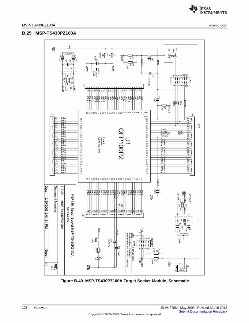
MSP-TS430PZ100A www.ti.com
B.25 MSP-TS430PZ100A
Figure B-49. MSP-TS430PZ100A Target Socket Module, Schematic
108 Hardware SLAU278M–May 2009–Revised March 2013Submit Documentation Feedback
Copyright © 2009–2013, Texas Instruments Incorporated
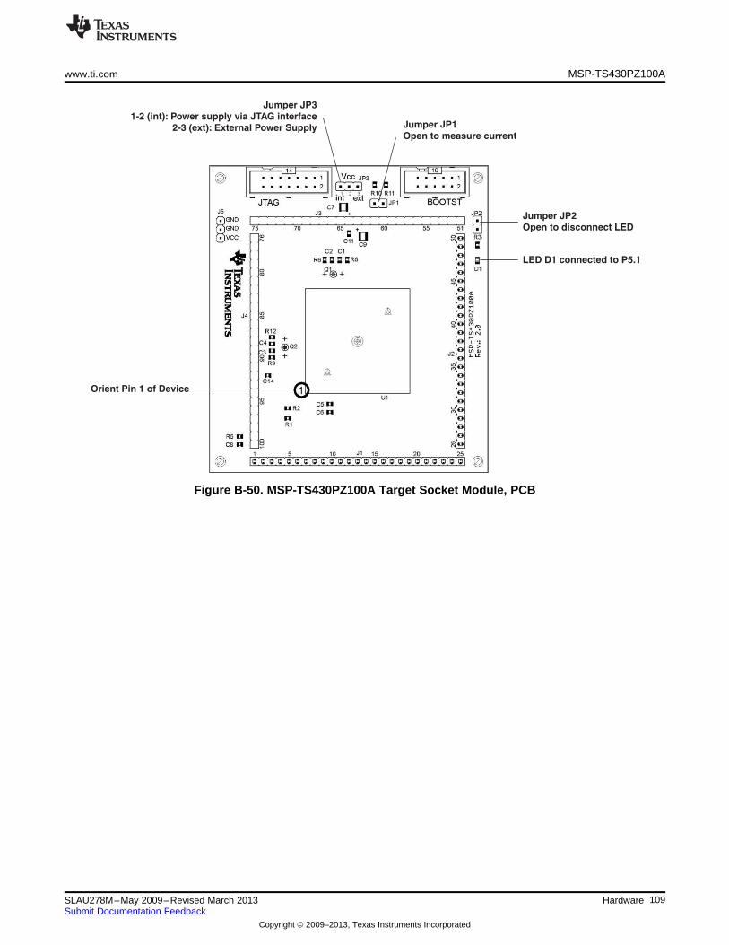
Jumper JP1
Open to measure current
Jumper JP2
Open to disconnect LED
LED D1 connected to P5.1
Jumper JP3
1-2 (int): Power supply via JTAG interface
2-3 (ext): External Power Supply
Orient Pin 1 of Device
www.ti.com MSP-TS430PZ100A
Figure B-50. MSP-TS430PZ100A Target Socket Module, PCB
109SLAU278M–May 2009–Revised March 2013 HardwareSubmit Documentation Feedback
Copyright © 2009–2013, Texas Instruments Incorporated
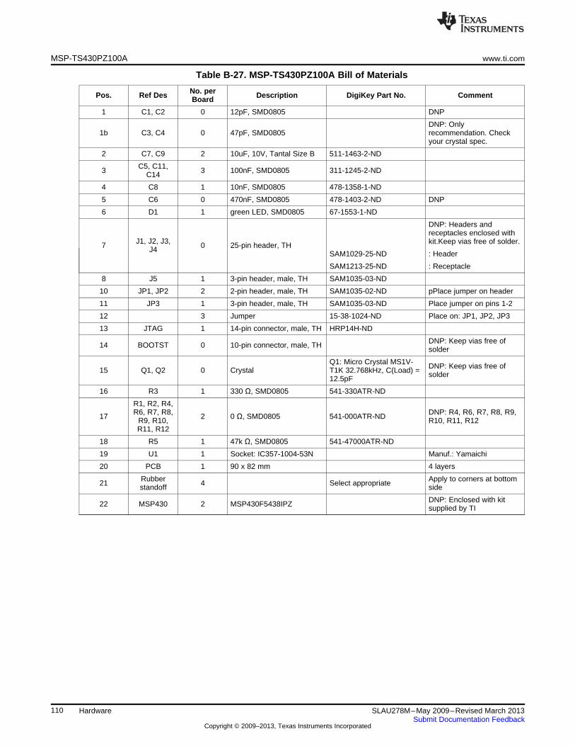
MSP-TS430PZ100A www.ti.com
Table B-27. MSP-TS430PZ100A Bill of Materials
No. perPos. Ref Des Description DigiKey Part No. CommentBoard
1 C1, C2 0 12pF, SMD0805 DNP
DNP: Only1b C3, C4 0 47pF, SMD0805 recommendation. Check
your crystal spec.
2 C7, C9 2 10uF, 10V, Tantal Size B 511-1463-2-ND
C5, C11,3 3 100nF, SMD0805 311-1245-2-NDC14
4 C8 1 10nF, SMD0805 478-1358-1-ND
5 C6 0 470nF, SMD0805 478-1403-2-ND DNP
6 D1 1 green LED, SMD0805 67-1553-1-ND
DNP: Headers andreceptacles enclosed with
J1, J2, J3, kit.Keep vias free of solder.7 0 25-pin header, THJ4 SAM1029-25-ND : Header
SAM1213-25-ND : Receptacle
8 J5 1 3-pin header, male, TH SAM1035-03-ND
10 JP1, JP2 2 2-pin header, male, TH SAM1035-02-ND pPlace jumper on header
11 JP3 1 3-pin header, male, TH SAM1035-03-ND Place jumper on pins 1-2
12 3 Jumper 15-38-1024-ND Place on: JP1, JP2, JP3
13 JTAG 1 14-pin connector, male, TH HRP14H-ND
DNP: Keep vias free of14 BOOTST 0 10-pin connector, male, TH solder
Q1: Micro Crystal MS1V- DNP: Keep vias free of15 Q1, Q2 0 Crystal T1K 32.768kHz, C(Load) = solder12.5pF
16 R3 1 330 Ω, SMD0805 541-330ATR-ND
R1, R2, R4,R6, R7, R8, DNP: R4, R6, R7, R8, R9,17 2 0 Ω, SMD0805 541-000ATR-NDR9, R10, R10, R11, R12R11, R12
18 R5 1 47k Ω, SMD0805 541-47000ATR-ND
19 U1 1 Socket: IC357-1004-53N Manuf.: Yamaichi
20 PCB 1 90 x 82 mm 4 layers
Rubber Apply to corners at bottom21 4 Select appropriatestandoff side
DNP: Enclosed with kit22 MSP430 2 MSP430F5438IPZ supplied by TI
110 Hardware SLAU278M–May 2009–Revised March 2013Submit Documentation Feedback
Copyright © 2009–2013, Texas Instruments Incorporated
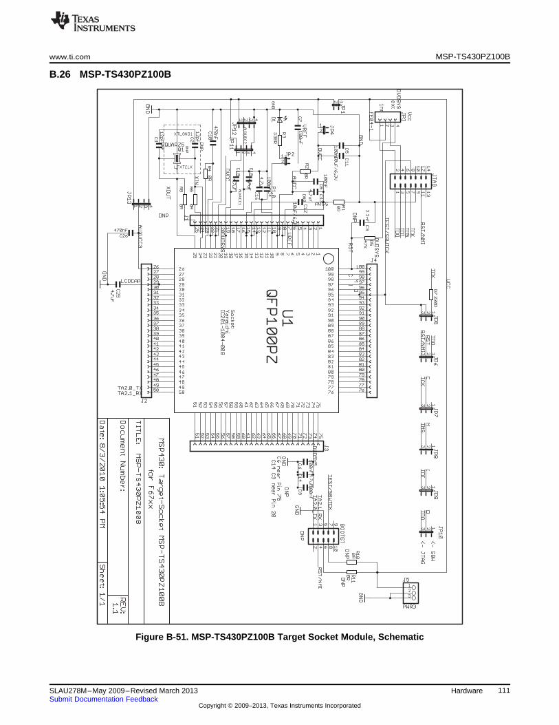
www.ti.com MSP-TS430PZ100B
B.26 MSP-TS430PZ100B
Figure B-51. MSP-TS430PZ100B Target Socket Module, Schematic
111SLAU278M–May 2009–Revised March 2013 HardwareSubmit Documentation Feedback
Copyright © 2009–2013, Texas Instruments Incorporated
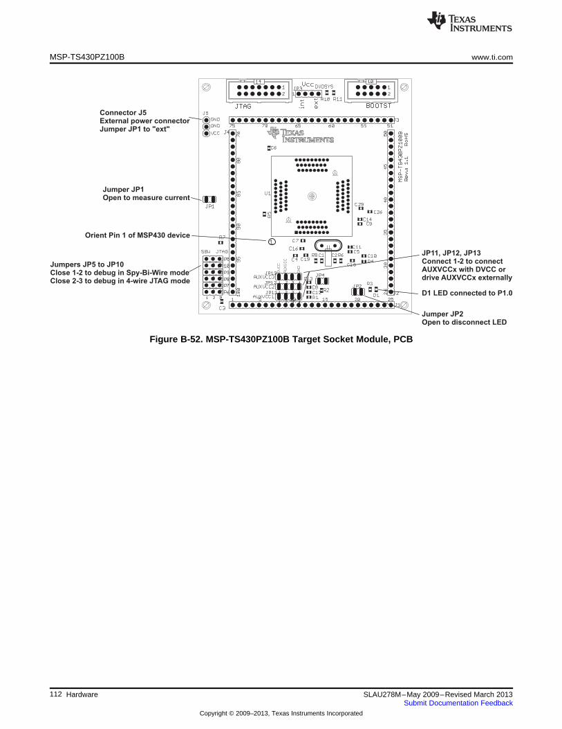
Connector J5External power connectorJumper JP1 to "ext"
Jumper JP1Open to measure current
Orient Pin 1 of MSP430 device
Jumpers JP5 to JP10Close 1-2 to debug in Spy-Bi-Wire modeClose 2-3 to debug in 4-wire JTAG mode
JP11, JP12, JP13Connect 1-2 to connectAUXVCCx with DVCC ordrive AUXVCCx externally
D1 LED connected to P1.0
Jumper JP2Open to disconnect LED
MSP-TS430PZ100B www.ti.com
Figure B-52. MSP-TS430PZ100B Target Socket Module, PCB
112 Hardware SLAU278M–May 2009–Revised March 2013Submit Documentation Feedback
Copyright © 2009–2013, Texas Instruments Incorporated
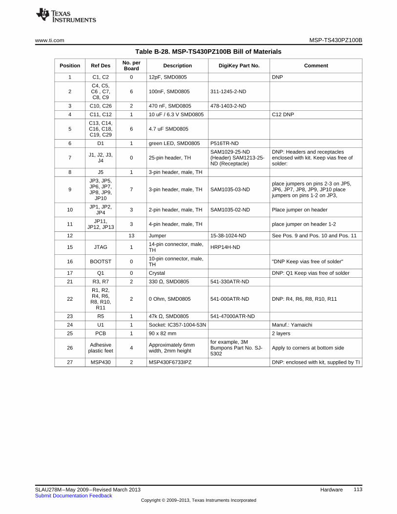
www.ti.com MSP-TS430PZ100B
Table B-28. MSP-TS430PZ100B Bill of Materials
No. perPosition Ref Des Description DigiKey Part No. CommentBoard
1 C1, C2 0 12pF, SMD0805 DNP
C4, C5,2 C6 , C7, 6 100nF, SMD0805 311-1245-2-ND
C8, C9
3 C10, C26 2 470 nF, SMD0805 478-1403-2-ND
4 C11, C12 1 10 uF / 6.3 V SMD0805 C12 DNP
C13, C14,5 C16, C18, 6 4.7 uF SMD0805
C19, C29
6 D1 1 green LED, SMD0805 P516TR-ND
SAM1029-25-ND DNP: Headers and receptaclesJ1, J2, J3,7 0 25-pin header, TH (Header) SAM1213-25- enclosed with kit. Keep vias free ofJ4 ND (Receptacle) solder:
8 J5 1 3-pin header, male, TH
JP3, JP5, place jumpers on pins 2-3 on JP5,JP6, JP7,9 7 3-pin header, male, TH SAM1035-03-ND JP6, JP7, JP8, JP9, JP10 placeJP8, JP9, jumpers on pins 1-2 on JP3,JP10
JP1, JP2,10 3 2-pin header, male, TH SAM1035-02-ND Place jumper on headerJP4
JP11,11 3 4-pin header, male, TH place jumper on header 1-2JP12, JP13
12 13 Jumper 15-38-1024-ND See Pos. 9 and Pos. 10 and Pos. 11
14-pin connector, male,15 JTAG 1 HRP14H-NDTH
10-pin connector, male,16 BOOTST 0 "DNP Keep vias free of solder"TH
17 Q1 0 Crystal DNP: Q1 Keep vias free of solder
21 R3, R7 2 330 Ω, SMD0805 541-330ATR-ND
R1, R2,R4, R6,22 2 0 Ohm, SMD0805 541-000ATR-ND DNP: R4, R6, R8, R10, R11R8, R10,
R11
23 R5 1 47k Ω, SMD0805 541-47000ATR-ND
24 U1 1 Socket: IC357-1004-53N Manuf.: Yamaichi
25 PCB 1 90 x 82 mm 2 layers
for example, 3MAdhesive Approximately 6mm26 4 Bumpons Part No. SJ- Apply to corners at bottom sideplastic feet width, 2mm height 5302
27 MSP430 2 MSP430F6733IPZ DNP: enclosed with kit, supplied by TI
113SLAU278M–May 2009–Revised March 2013 HardwareSubmit Documentation Feedback
Copyright © 2009–2013, Texas Instruments Incorporated
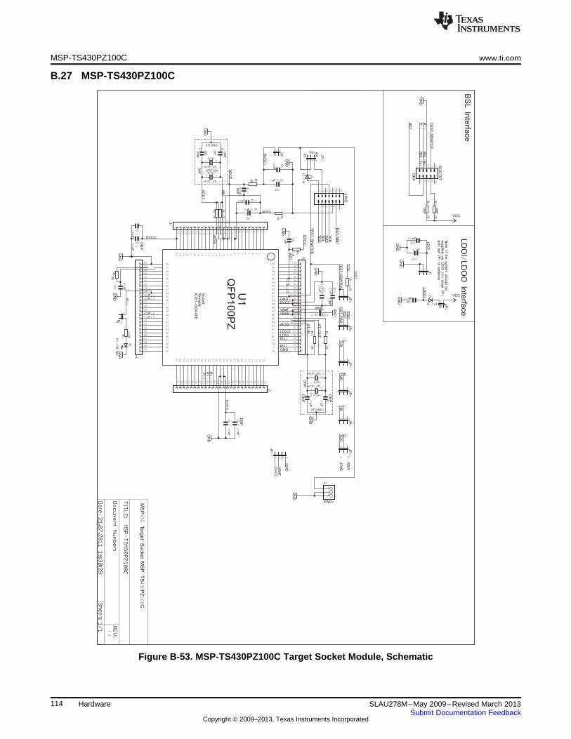
DN
PD
NP
DN
P
DN
P
DN
P
DN
P
0R
12pF
12pF
47pF
47pF
GN
D
0R
100nF
330R
10 /6.3uF V
10 /6.3uF V
2.2
nF
PWR3
GN
D
GN
D
GN
D
GN
D0R
330R
47K
100nF
100nF
PT
RN
D516
-
470nF
100nF
100nF
0R
0R
0R
0R
GN
D
VCC
100nF
GN
D
100nF
100nF
GN
D
100nF
LL
A103
GN
D
4.7n
HCTC XTL_ _4
HCTC XTL_ _4
HCTC XTL_ _4
HCTC XTL_ _4
GN
D
0R
0R
GN
DG
ND
GN
D
4.7uF
GN
D
100nF
220nF
GN
D
VCC
LL A103
1.1
MS
PTa
rge
tS
ocke
tM
SP
TS
PZ
C430:
--
430
100
Socket:
Ya
maich
iIC
201-1
004-0
08
LFXTCLK
<-
SB
W
<-
JTA
G
Vccint
ext
DN
P
DN
P
DN
P
DN
P
DN
P
DN
P
BS
LR
x-
BS
LT
x-
DN
P
1 3 5 7 9 11 13
2 4 6
12
148
10
JTA
G
R2
C2
C1
C3
C4
R1
C5
R3
C6
C7
C8
123
J5
8079787776
75
74
73
72
71
70
69
68
67
66
65
60
59
58
57
56
55
54
53
52
51
504948474645
3635343332313029282726
25
24
23
22
21
16
15
14
13
12
11 10
9 8 7 6 5 4 3 2 1
64
63
62
61
44434241
37383940
17
18
19
20
81828384858687888990919293949596979899
100
U1
QF
P1
00
PZ
12345678910
1112
13
14
15
16
17
18
19
20
21
22
23
24
25
J1
26272829303132333435363738394041424344454647484950
J2
51
52
53
54
55
56
57
58
59
60
61
62
63
64
65
66
67
68
69
70
71
72
73
74
75
J3
767778798081828384858687888990919293949596979899
100
J4
1JP
1
2
1
JP2
2
R4
123
JP
5123
JP
6123
JP
7123
JP
8123
JP
9123
JP
10
R7
R5
C11
C12
D1
C9
C13
C10
R6
R8
R9
R12
1 2 3
JP
3
C17
C18
C19
C14
D3
C16
1 2 3
JP
11
4
21Q G1 $1
43Q G1 $2
2 1
Q G2 $1
4 3
Q G2 $2
12
34
56
78
910
BO
OT
ST
R10
R11
C15
C20
C21
1JP
4
2
D4
123
J6
TM
S
TM
S
TD
I
TD
I
TD
O
TD
O
TD
O
XO
UT
VC
C
GND
GND
GN
D
XIN
P1.0
DV
CC
1
DV
CC
1
DV
CC
1
DVCC1
DV
CC
1
DVCC1
AV
CC
XT
OU
T2
AVSS
AVSS
AV
SS
M
M
I
I
O
O
XT
IN2
RS
TN
MI
/R
ST
NM
I/
TC
K
TC
K
TC
KC
C
TE
ST
SB
WT
CK
/
TE
ST
SB
WT
CK
/
TE
ST
SB
WT
CK
/
RS
T
RS
T
RS
T
XTLGND2
XTLGND1
PU.0
PU.1
P1.6P1.7
P8.0
P8.1
P8.2
VBAKVBAT
VBAT
VB
AT
P1.1
P1.1
P1.2
P1.2
LD
OI
LDOI
LD
OO
LDOO
BS
LIn
terfa
ce
LD
OI
LD
OO
Inte
rface
/
+
+
Note
Ifth
esys
tem
should
be
:supplie
dvia
LD
OI
Jclo
se
JP
(6)
4and
set
JP
toexte
rnal
3
MSP-TS430PZ100C www.ti.com
B.27 MSP-TS430PZ100C
Figure B-53. MSP-TS430PZ100C Target Socket Module, Schematic
114 Hardware SLAU278M–May 2009–Revised March 2013Submit Documentation Feedback
Copyright © 2009–2013, Texas Instruments Incorporated
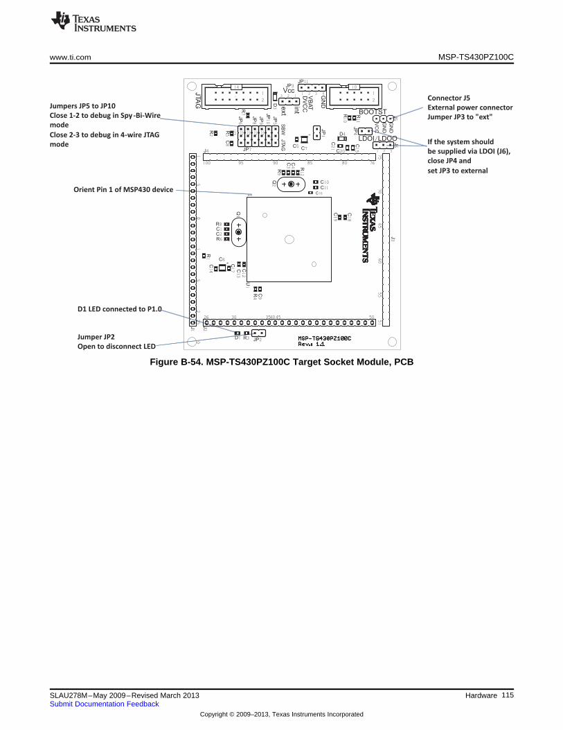
Connector J5
External power connector
Jumper JP3 to "ext"
If the system should
be supplied via LDOI (J6),
close JP4 and
set JP3 to external
Jumper JP2
Open to disconnect LED
D1 LED connected to P1.0
Orient Pin 1 of MSP430 device
Jumpers JP5 to JP10
Close 1-2 to debug in Spy -Bi-Wire
mode
Close 2-3 to debug in 4-wire JTAG
modeLDOI LDOO/
14
1
2
GN
D
GN
D
VC
C
125
510
15
20
26 5030 3540 45 51
75
55
60
65
70
76100 80859095
12
3
123
123
123
123
123
1231 2 3 4
10
1
2
1 2 3
1
JTA
GS
BW
Vcc
int
ext
GN
D
VB
AT
DV
CC
JTA
G
R2
C2
C1
C3
C4
R1
C5
R3+C6
+
C7
C8
J5
U1
J1
J2
J3
J4
JP
1
JP2
R4
JP
5
JP
6
JP7
JP
8
JP
9
JP
10
R7
R5
C11
C12
D1
C9
C13
C10
R6
R8
R9
R12
JP3
C17
C18
C19
C14
D3
C16
JP11
Q1
Q2
BOOTSTR10
R11
C15
C20
C21
JP
4
D4
J6
www.ti.com MSP-TS430PZ100C
Figure B-54. MSP-TS430PZ100C Target Socket Module, PCB
115SLAU278M–May 2009–Revised March 2013 HardwareSubmit Documentation Feedback
Copyright © 2009–2013, Texas Instruments Incorporated
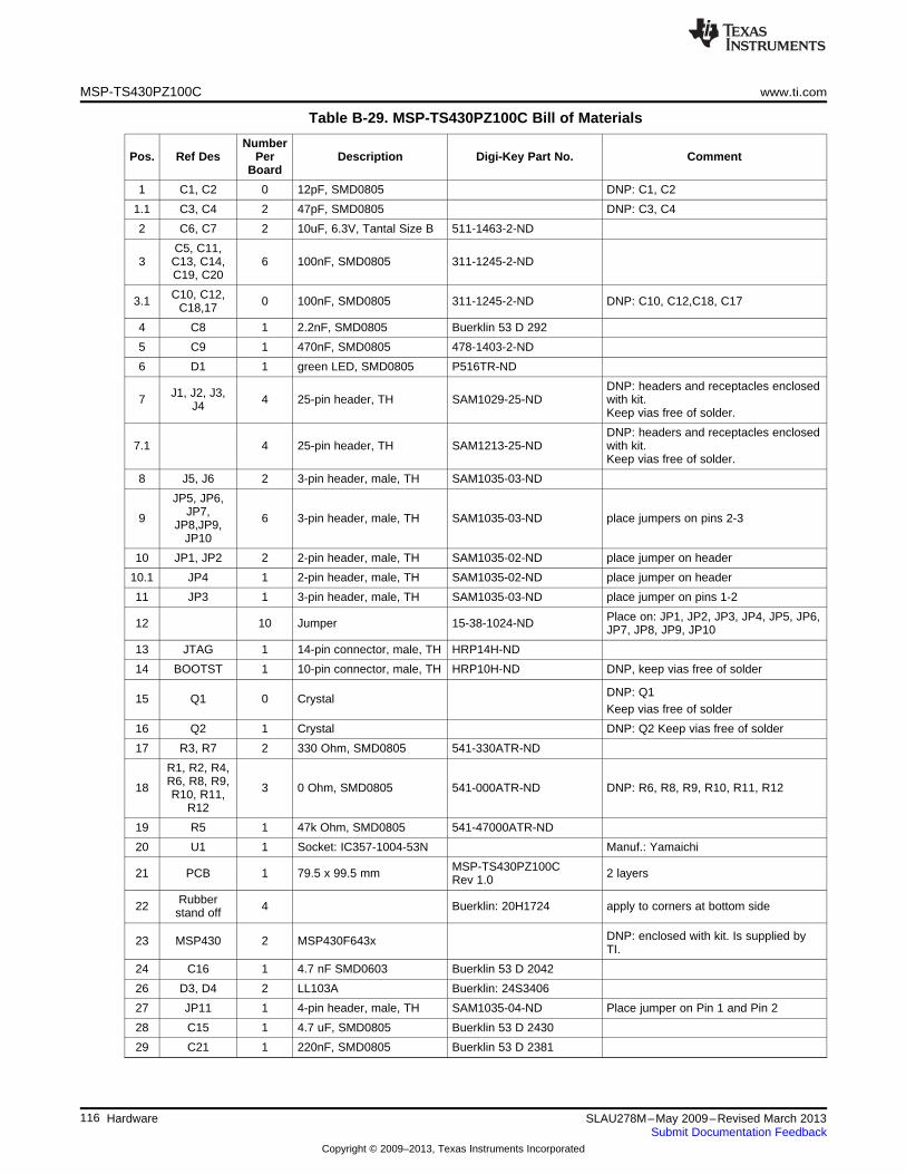
MSP-TS430PZ100C www.ti.com
Table B-29. MSP-TS430PZ100C Bill of Materials
NumberPos. Ref Des Per Description Digi-Key Part No. Comment
Board
1 C1, C2 0 12pF, SMD0805 DNP: C1, C2
1.1 C3, C4 2 47pF, SMD0805 DNP: C3, C4
2 C6, C7 2 10uF, 6.3V, Tantal Size B 511-1463-2-ND
C5, C11,3 C13, C14, 6 100nF, SMD0805 311-1245-2-ND
C19, C20
C10, C12,3.1 0 100nF, SMD0805 311-1245-2-ND DNP: C10, C12,C18, C17C18,17
4 C8 1 2.2nF, SMD0805 Buerklin 53 D 292
5 C9 1 470nF, SMD0805 478-1403-2-ND
6 D1 1 green LED, SMD0805 P516TR-ND
DNP: headers and receptacles enclosedJ1, J2, J3,7 4 25-pin header, TH SAM1029-25-ND with kit.J4 Keep vias free of solder.
DNP: headers and receptacles enclosed7.1 4 25-pin header, TH SAM1213-25-ND with kit.
Keep vias free of solder.
8 J5, J6 2 3-pin header, male, TH SAM1035-03-ND
JP5, JP6,JP7,9 6 3-pin header, male, TH SAM1035-03-ND place jumpers on pins 2-3JP8,JP9,JP10
10 JP1, JP2 2 2-pin header, male, TH SAM1035-02-ND place jumper on header
10.1 JP4 1 2-pin header, male, TH SAM1035-02-ND place jumper on header
11 JP3 1 3-pin header, male, TH SAM1035-03-ND place jumper on pins 1-2
Place on: JP1, JP2, JP3, JP4, JP5, JP6,12 10 Jumper 15-38-1024-ND JP7, JP8, JP9, JP10
13 JTAG 1 14-pin connector, male, TH HRP14H-ND
14 BOOTST 1 10-pin connector, male, TH HRP10H-ND DNP, keep vias free of solder
DNP: Q115 Q1 0 CrystalKeep vias free of solder
16 Q2 1 Crystal DNP: Q2 Keep vias free of solder
17 R3, R7 2 330 Ohm, SMD0805 541-330ATR-ND
R1, R2, R4,R6, R8, R9,18 3 0 Ohm, SMD0805 541-000ATR-ND DNP: R6, R8, R9, R10, R11, R12R10, R11,
R12
19 R5 1 47k Ohm, SMD0805 541-47000ATR-ND
20 U1 1 Socket: IC357-1004-53N Manuf.: Yamaichi
MSP-TS430PZ100C21 PCB 1 79.5 x 99.5 mm 2 layersRev 1.0
Rubber22 4 Buerklin: 20H1724 apply to corners at bottom sidestand off
DNP: enclosed with kit. Is supplied by23 MSP430 2 MSP430F643xTI.
24 C16 1 4.7 nF SMD0603 Buerklin 53 D 2042
26 D3, D4 2 LL103A Buerklin: 24S3406
27 JP11 1 4-pin header, male, TH SAM1035-04-ND Place jumper on Pin 1 and Pin 2
28 C15 1 4.7 uF, SMD0805 Buerklin 53 D 2430
29 C21 1 220nF, SMD0805 Buerklin 53 D 2381
116 Hardware SLAU278M–May 2009–Revised March 2013Submit Documentation Feedback
Copyright © 2009–2013, Texas Instruments Incorporated
www.ti.com MSP-TS430PZ100C
117SLAU278M–May 2009–Revised March 2013 HardwareSubmit Documentation Feedback
Copyright © 2009–2013, Texas Instruments Incorporated
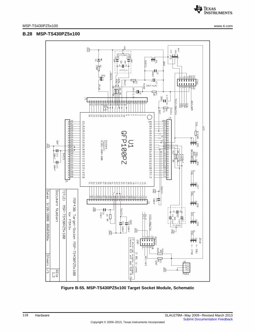
MSP-TS430PZ5x100 www.ti.com
B.28 MSP-TS430PZ5x100
Figure B-55. MSP-TS430PZ5x100 Target Socket Module, Schematic
118 Hardware SLAU278M–May 2009–Revised March 2013Submit Documentation Feedback
Copyright © 2009–2013, Texas Instruments Incorporated
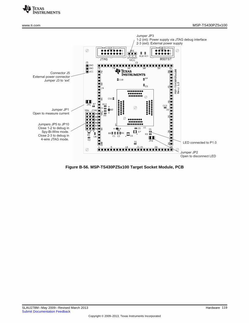
Connector J5External power connector
Jumper J3 to ‘ext’
Jumper JP1Open to measure current
Jumpers JP5 to JP10Close 1-2 to debug in
Spy-Bi-Wire mode.Close 2-3 to debug in
4-wire JTAG mode.
Jumper JP2Open to disconnect LED
LED connected to P1.0
Jumper JP31-2 (int): Power supply via JTAG debug interface2-3 (ext): External power supply
www.ti.com MSP-TS430PZ5x100
Figure B-56. MSP-TS430PZ5x100 Target Socket Module, PCB
119SLAU278M–May 2009–Revised March 2013 HardwareSubmit Documentation Feedback
Copyright © 2009–2013, Texas Instruments Incorporated
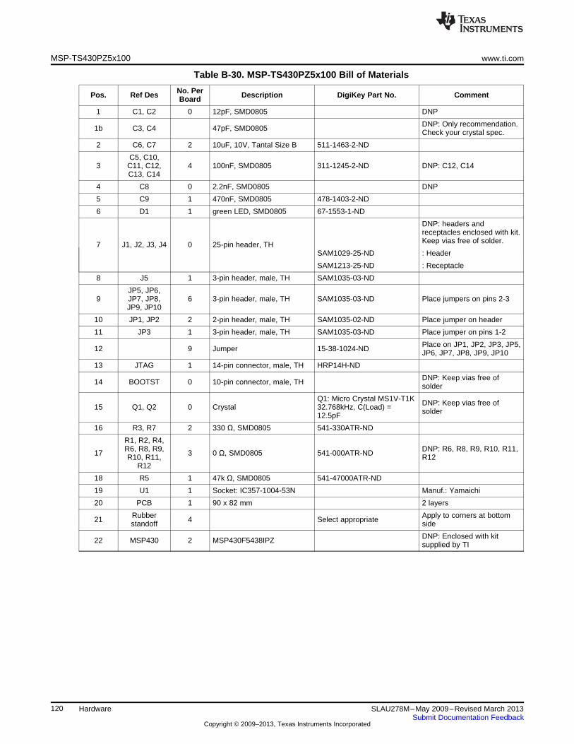
MSP-TS430PZ5x100 www.ti.com
Table B-30. MSP-TS430PZ5x100 Bill of Materials
No. PerPos. Ref Des Description DigiKey Part No. CommentBoard
1 C1, C2 0 12pF, SMD0805 DNP
DNP: Only recommendation.1b C3, C4 47pF, SMD0805 Check your crystal spec.
2 C6, C7 2 10uF, 10V, Tantal Size B 511-1463-2-ND
C5, C10,3 C11, C12, 4 100nF, SMD0805 311-1245-2-ND DNP: C12, C14
C13, C14
4 C8 0 2.2nF, SMD0805 DNP
5 C9 1 470nF, SMD0805 478-1403-2-ND
6 D1 1 green LED, SMD0805 67-1553-1-ND
DNP: headers andreceptacles enclosed with kit.Keep vias free of solder.7 J1, J2, J3, J4 0 25-pin header, TH
SAM1029-25-ND : Header
SAM1213-25-ND : Receptacle
8 J5 1 3-pin header, male, TH SAM1035-03-ND
JP5, JP6,9 JP7, JP8, 6 3-pin header, male, TH SAM1035-03-ND Place jumpers on pins 2-3
JP9, JP10
10 JP1, JP2 2 2-pin header, male, TH SAM1035-02-ND Place jumper on header
11 JP3 1 3-pin header, male, TH SAM1035-03-ND Place jumper on pins 1-2
Place on JP1, JP2, JP3, JP5,12 9 Jumper 15-38-1024-ND JP6, JP7, JP8, JP9, JP10
13 JTAG 1 14-pin connector, male, TH HRP14H-ND
DNP: Keep vias free of14 BOOTST 0 10-pin connector, male, TH solder
Q1: Micro Crystal MS1V-T1K DNP: Keep vias free of15 Q1, Q2 0 Crystal 32.768kHz, C(Load) = solder12.5pF
16 R3, R7 2 330 Ω, SMD0805 541-330ATR-ND
R1, R2, R4,R6, R8, R9, DNP: R6, R8, R9, R10, R11,17 3 0 Ω, SMD0805 541-000ATR-NDR10, R11, R12
R12
18 R5 1 47k Ω, SMD0805 541-47000ATR-ND
19 U1 1 Socket: IC357-1004-53N Manuf.: Yamaichi
20 PCB 1 90 x 82 mm 2 layers
Rubber Apply to corners at bottom21 4 Select appropriatestandoff side
DNP: Enclosed with kit22 MSP430 2 MSP430F5438IPZ supplied by TI
120 Hardware SLAU278M–May 2009–Revised March 2013Submit Documentation Feedback
Copyright © 2009–2013, Texas Instruments Incorporated
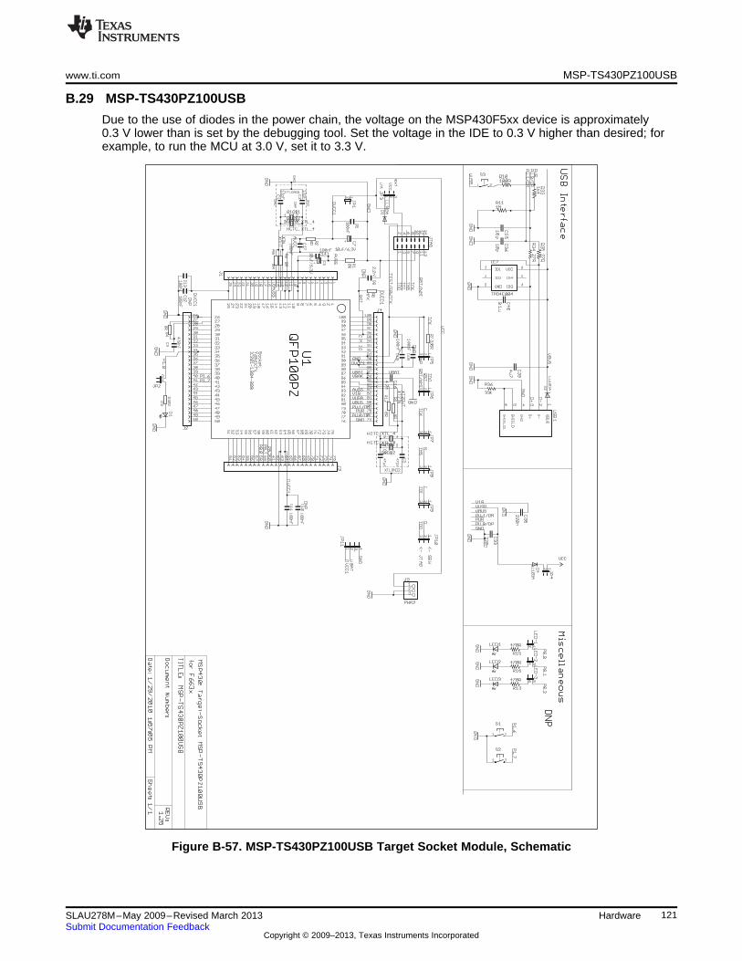
www.ti.com MSP-TS430PZ100USB
B.29 MSP-TS430PZ100USB
Due to the use of diodes in the power chain, the voltage on the MSP430F5xx device is approximately0.3 V lower than is set by the debugging tool. Set the voltage in the IDE to 0.3 V higher than desired; forexample, to run the MCU at 3.0 V, set it to 3.3 V.
Figure B-57. MSP-TS430PZ100USB Target Socket Module, Schematic
121SLAU278M–May 2009–Revised March 2013 HardwareSubmit Documentation Feedback
Copyright © 2009–2013, Texas Instruments Incorporated
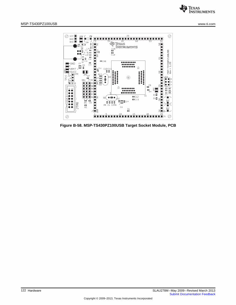
MSP-TS430PZ100USB www.ti.com
Figure B-58. MSP-TS430PZ100USB Target Socket Module, PCB
122 Hardware SLAU278M–May 2009–Revised March 2013Submit Documentation Feedback
Copyright © 2009–2013, Texas Instruments Incorporated
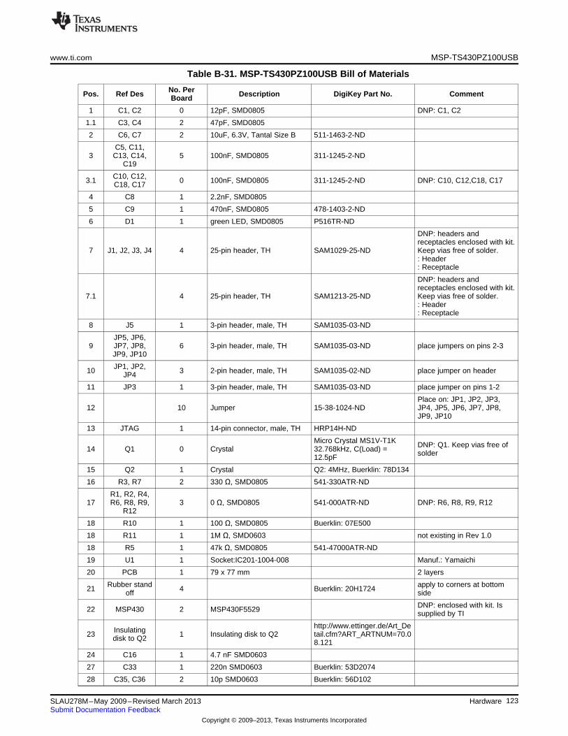
www.ti.com MSP-TS430PZ100USB
Table B-31. MSP-TS430PZ100USB Bill of Materials
No. PerPos. Ref Des Description DigiKey Part No. CommentBoard
1 C1, C2 0 12pF, SMD0805 DNP: C1, C2
1.1 C3, C4 2 47pF, SMD0805
2 C6, C7 2 10uF, 6.3V, Tantal Size B 511-1463-2-ND
C5, C11,3 C13, C14, 5 100nF, SMD0805 311-1245-2-ND
C19
C10, C12,3.1 0 100nF, SMD0805 311-1245-2-ND DNP: C10, C12,C18, C17C18, C17
4 C8 1 2.2nF, SMD0805
5 C9 1 470nF, SMD0805 478-1403-2-ND
6 D1 1 green LED, SMD0805 P516TR-ND
DNP: headers andreceptacles enclosed with kit.
7 J1, J2, J3, J4 4 25-pin header, TH SAM1029-25-ND Keep vias free of solder.: Header: Receptacle
DNP: headers andreceptacles enclosed with kit.
7.1 4 25-pin header, TH SAM1213-25-ND Keep vias free of solder.: Header: Receptacle
8 J5 1 3-pin header, male, TH SAM1035-03-ND
JP5, JP6,9 JP7, JP8, 6 3-pin header, male, TH SAM1035-03-ND place jumpers on pins 2-3
JP9, JP10
JP1, JP2,10 3 2-pin header, male, TH SAM1035-02-ND place jumper on headerJP4
11 JP3 1 3-pin header, male, TH SAM1035-03-ND place jumper on pins 1-2
Place on: JP1, JP2, JP3,12 10 Jumper 15-38-1024-ND JP4, JP5, JP6, JP7, JP8,
JP9, JP10
13 JTAG 1 14-pin connector, male, TH HRP14H-ND
Micro Crystal MS1V-T1K DNP: Q1. Keep vias free of14 Q1 0 Crystal 32.768kHz, C(Load) = solder12.5pF
15 Q2 1 Crystal Q2: 4MHz, Buerklin: 78D134
16 R3, R7 2 330 Ω, SMD0805 541-330ATR-ND
R1, R2, R4,17 R6, R8, R9, 3 0 Ω, SMD0805 541-000ATR-ND DNP: R6, R8, R9, R12
R12
18 R10 1 100 Ω, SMD0805 Buerklin: 07E500
18 R11 1 1M Ω, SMD0603 not existing in Rev 1.0
18 R5 1 47k Ω, SMD0805 541-47000ATR-ND
19 U1 1 Socket:IC201-1004-008 Manuf.: Yamaichi
20 PCB 1 79 x 77 mm 2 layers
Rubber stand apply to corners at bottom21 4 Buerklin: 20H1724off side
DNP: enclosed with kit. Is22 MSP430 2 MSP430F5529 supplied by TI
http://www.ettinger.de/Art_DeInsulating23 1 Insulating disk to Q2 tail.cfm?ART_ARTNUM=70.0disk to Q2 8.121
24 C16 1 4.7 nF SMD0603
27 C33 1 220n SMD0603 Buerklin: 53D2074
28 C35, C36 2 10p SMD0603 Buerklin: 56D102
123SLAU278M–May 2009–Revised March 2013 HardwareSubmit Documentation Feedback
Copyright © 2009–2013, Texas Instruments Incorporated
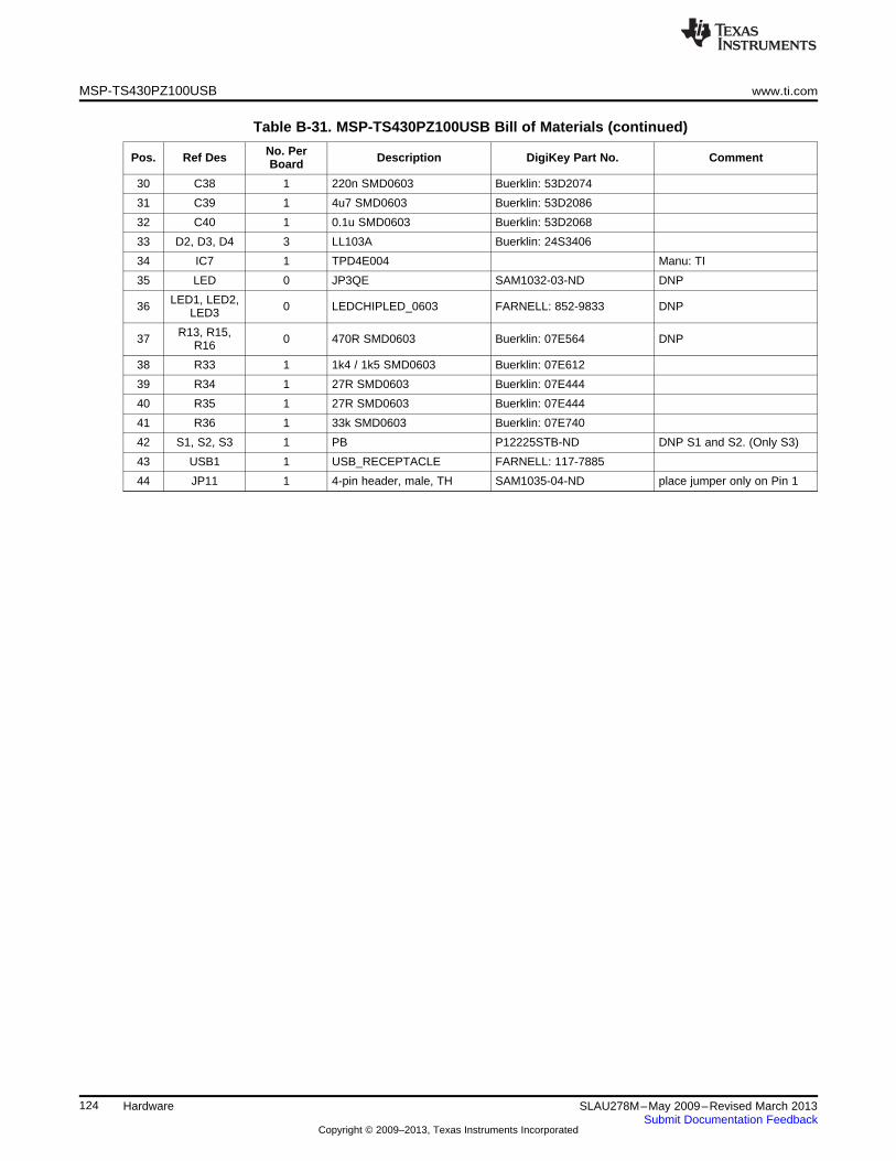
MSP-TS430PZ100USB www.ti.com
Table B-31. MSP-TS430PZ100USB Bill of Materials (continued)
No. PerPos. Ref Des Description DigiKey Part No. CommentBoard
30 C38 1 220n SMD0603 Buerklin: 53D2074
31 C39 1 4u7 SMD0603 Buerklin: 53D2086
32 C40 1 0.1u SMD0603 Buerklin: 53D2068
33 D2, D3, D4 3 LL103A Buerklin: 24S3406
34 IC7 1 TPD4E004 Manu: TI
35 LED 0 JP3QE SAM1032-03-ND DNP
LED1, LED2,36 0 LEDCHIPLED_0603 FARNELL: 852-9833 DNPLED3
R13, R15,37 0 470R SMD0603 Buerklin: 07E564 DNPR16
38 R33 1 1k4 / 1k5 SMD0603 Buerklin: 07E612
39 R34 1 27R SMD0603 Buerklin: 07E444
40 R35 1 27R SMD0603 Buerklin: 07E444
41 R36 1 33k SMD0603 Buerklin: 07E740
42 S1, S2, S3 1 PB P12225STB-ND DNP S1 and S2. (Only S3)
43 USB1 1 USB_RECEPTACLE FARNELL: 117-7885
44 JP11 1 4-pin header, male, TH SAM1035-04-ND place jumper only on Pin 1
124 Hardware SLAU278M–May 2009–Revised March 2013Submit Documentation Feedback
Copyright © 2009–2013, Texas Instruments Incorporated
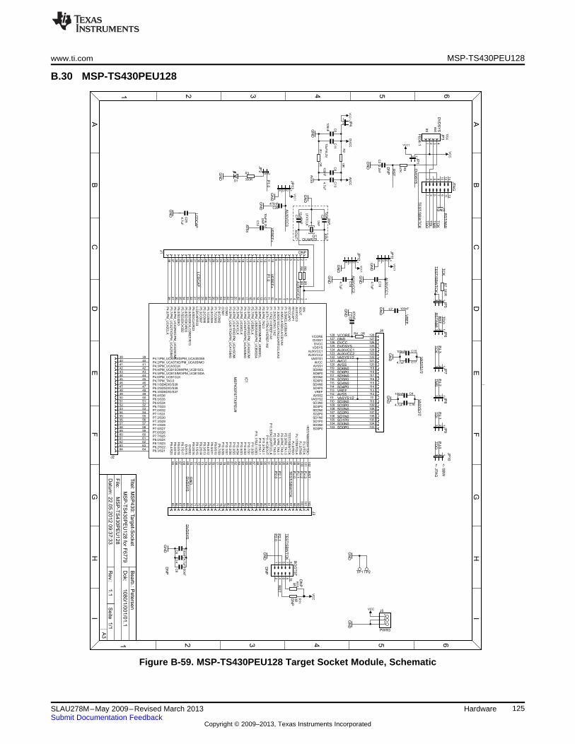
0R
12pF
12pF
GN
D
GN
D
0R
100nF
330R
2.2
nF
0R
0R
PWR3
GN
D
330R
47K
0R
0R
100nF
4.7
uF
GN
D
GN
D
100nF470nF
0R
QUARZ5
100nF
10uF
/6,3
V
10uF
/6,3
V
100nF
4.7
uF
4.7
uF
100nF
4.7uF
4.7
uF
4.7
uF
470nF
FE
04-1
VC
C
GN
D
GN
D
100nF
4.7uF
GN
D
GN
D
GN
D
GN
D
GN
D
VCC1
VC
C1
VC
C1
VC
C1
VC
C1
GN
D
GN
D
GN
D
GN
D
GN
D
GN
D
AV
SS
AV
SS
AV
CC
DV
CC
GND
VC
C
VCC
GN
D
MS
P4
30
:Ta
rge
t-So
cke
t
MS
P-T
S4
30
PE
U1
28
for
F6
77
9
Pe
ters
en
10
80
/1/0
01
/01
.1
DN
P
LF
XT
CL
K
DN
P
<-
SB
W
<-
JTA
G
DN
P
Vcc
int
ext
DN
P
DN
P
DN
P
DNP
DN
P
DN
P
DN
P
DV
DS
YS
1.1
12345678910
1112
13
14
15
16
17
18
19
20
21
22
23
24
25
26
27
28
29
30
31
32
33
34
35
36
37
38
J1
39
40
41
42
43
44
45
46
47
48
49
50
51
52
53
54
55
56
57
58
59
60
61
62
63
64
J2
65
66
67
68
69
70
71
72
73
74
75
76
77
78
79
80
81
82
83
84
85
86
87
88
89
90
91
92
93
94
95
96
97
98
99
100
101
102
J3
103
104
105
106
107
108
109
110
111
112
113
114
115
116
117
118
119
120
121
122
123
124
125
126127
128
J4
1 3 5 7 9 11 13
2 4 6
12
148
10
JTA
G
R2
C2
C1
R1
C5
R3
12
34
56
78
910
BO
OT
ST
C3
R10
R11
J51
2
3
12
JP
1
JP
2
1 2
123
JP
5123
JP
6123
JP
7123
JP
8123
JP
9123 JP
10
R7
R5
D1
R6
R8
C6
C29
C7
C10
R4
Q1
JP
12
1234
1234
JP
11
JP
13
1234
C4
C11
C12
C8
C13
C14
C9
C16
C19
C18
C26
1
2
JP
4
JP
3
1 2 3 4
C15
C17
TP1 TP2
IC1
MS
P430F
677X
IPE
U#
XIN
1
XO
UT
2
AU
XV
CC
33
RT
CC
AP
14
RT
CC
AP
05
P1.5
/SM
CLK
/CB
0/A
56
P1.4
/MC
LK
/SD
CLK
/CB
1/A
47
P1.3
/AD
C10C
LK
/TA
CLK
/RT
CC
LK
/A3
8
P1.2
/AC
LK
/TA
3.1
/A2
9
P1.1
/TA
2.1
/VE
RE
F+
/A1
10
P1.0
/TA
1.1
/TA
0.0
/VE
RE
F-/A
011
P2.4
/PM
_TA
2.0
12
P2.5
/PM
_U
CB
0S
OM
I/PM
_U
CB
0S
CL
13
P2.6
/PM
_U
SB
0S
IMO
/PM
_U
CB
0S
DA
14
P2.7
/PM
_U
CB
0C
LK
15
P3.0
/PM
_U
CA
0R
XD
/PM
_U
CA
0S
OM
I16
P3.1
/PM
_U
CA
0T
XD
/PM
_U
CA
0S
IMO
17
P3.2
/PM
_U
CA
0C
LK
18
P3.3
/PM
_U
CA
1C
LK
19
P3.4
/PM
_U
CA
1R
XD
/PM
_U
CA
1S
OM
I20
P3.5
/PM
_U
CA
1T
XD
/PM
_U
CA
1S
IMO
21
CO
M0
22
CO
M1
23
P1.6
/CO
M2
24
P1.7
/CO
M3
25
P5.0
/CO
M4
26
P5.1
/CO
M5
27
P5.2
/CO
M6
28
P5.3
/CO
M7
29
LC
DC
AP
/R33
30
P5.4
/SD
CLK
/R23
31
P5.5
/SD
0D
IO/L
CD
RE
F/R
13
32
P5.6
/SD
1D
IO/R
03
33
P5.7
/SD
2D
IO/C
B2
34
P6.0
/SD
3D
IO35
P3.6
/PM
_U
CA
2R
XD
/PM
_U
CA
2S
OM
I36
P3.7
/PM
_U
CA
2T
XD
/PM
_U
CA
2S
IMO
37
P4.0
/PM
_U
CA
2C
LK
38
P4.1/PM_UCA3RXD/PM_UCA3SOMI39
P4.2/PM_UCA3TXD/PM_UCA3SIMO40
P4.3/PM_UCA3CLK41
P4.4/PM_UCB1SOMI/PM_UCB1SCL42
P4.5/PM_UCB1SIMO/PM_UCB1SDA43
P4.6/PM_UCB1CLK44
P4.7/PM_TA3.045
P6.1/SD4DIO/S3946
P6.2/SD5DIO/S3847
P6.3/SD6DIO/S3748
P6.4/S3649
P6.5/S3550
P6.6/S3451
P6.7/S3352
P7.0/S3253
P7.1/S3154
P7.2/S3055
P7.3/S2956
P7.4/S2857
P7.5/S2758
P7.6/S2659
P7.7/S2560
P8.0/S2461
P8.1/S2362
P8.2/S2263
P8.3/S2164
P8.4
/S20
65
P8.5
/S19
66
P8.6
/S18
67
P8.7
/S17
68
DV
SY
S69
DV
SS
270
P9.0
/S16
71
P9.1
/S15
72
P9.2
/S14
73
P9.3
/S13
74
P9.4
/S12
75
P9.5
/S11
76
P9.6
/S10
77
P9.7
/S9
78
P10.0
/S8
79
P10.1
/S7
80
P10.2
/S6
81
P10.3
/S5
82
P10.4
/S4
83
P10.5
/S3
84
P10.6
/S2
85
P10.7
/S1
86
P11
.0/S
087
P11
.1/T
A3.1
/CB
388
P11
.2/T
A1.1
89
P11
.3/T
A2.1
90
P11
.4/C
BO
UT
91
P11
.5/T
AC
LK
/RT
CC
LK
92
P2.0
/PM
_TA
0.0
93
P2.1
/PM
_TA
0.1
94
P2.2
/PM
_TA
0.2
95
P2.3
/PM
_TA
1.0
96
TE
ST
/SB
WT
CK
97
PJ.0
/TD
O98
PJ.1
/TD
I/TC
LK
99
PJ.2
/TM
S100
PJ.3
/TC
K101
~R
ST
/NM
I/SB
WT
DIO
102
SD0P0103
SD0N0104
SD1P0105
SD1N0106
SD2P0107
SD2N0108
SD3P0109
SD3N0110
VASYS2111
AVSS2112
VREF113
SD4P0114
SD4N0115
SD5P0116
SD5N0117
SD6P0118
SD6N0119
AVSS1120
AVCC121
VASYS1122
AUXVCC2123
AUXVCC1124
VDSYS125
DVCC126
DVSS1127
VCORE128
P1.0
P1.0
P2.0
P2.0
P2.1
P2.1
SD0P0SD0N0SD1P0SD1N0SD2P0SD2N0SD3P0SD3N0
SD4P0SD4N0SD5P0SD5N0SD6P0SD6N0
VA
SY
S1/2
VASYS1/2
VASYS1/2
VA
SY
S1/2
TM
ST
MS
TD
I
TD
I
TD
O
TD
O
TD
O
XO
UT
GN
D
GND
XIN
DVCC
AVCC
DV
DS
YS
DV
DS
YS
DV
DS
YS
DVDSYS
AVSS
AVSS
PJ.2
PJ.2
PJ.1
PJ.1
PJ.0
PJ.0
RS
T/N
MI
RS
T/N
MI
TC
K
TC
K
TC
KP
J.3
PJ.3
TE
ST
/SB
WT
CK
TE
ST
/SB
WT
CK
TE
ST
/SB
WT
CK
TE
ST
/SB
WT
CK
RS
T
RS
T
RS
T
RS
T
LC
DC
AP
LC
DC
AP
VR
EF
VREF
VE
RE
F+
VE
RE
F+
VCORE
AU
XV
CC
2
AUXVCC2
AU
XV
CC
1
AUXVCC1
AU
XV
CC
3
AU
XV
CC
3
1 2 3 4 5 6
1 2 3 4 5 6
Tite
l:
Da
tum
:
Be
arb
.:
Se
ite1
/1
MS
P-T
S4
30
PE
U1
28
22
.05
.20
12
09
:37
:33
A3
IH
GF
ED
CB
A AB
CD
EF
GH
I
File
:
Do
k:
Re
v.:
www.ti.com MSP-TS430PEU128
B.30 MSP-TS430PEU128
Figure B-59. MSP-TS430PEU128 Target Socket Module, Schematic
125SLAU278M–May 2009–Revised March 2013 HardwareSubmit Documentation Feedback
Copyright © 2009–2013, Texas Instruments Incorporated
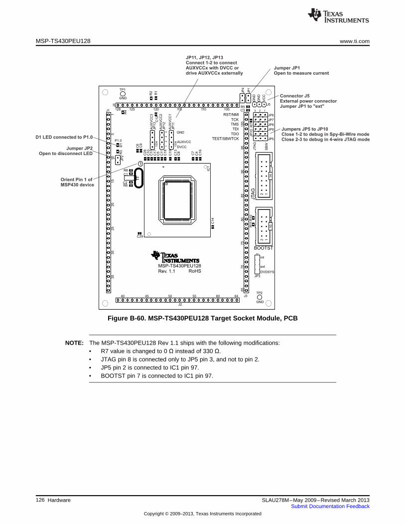
1
P1.0
SB
W
JTA
G
DVDSYS
ext
int
MSP-TS430PEU128
Rev. 1.1 RoHS
DVCC
AUXVCC
GND
AU
XV
CC
1
AU
XV
CC
2
AU
XV
CC
3
GND
GND
RST/NMI
TCK
TDI
TDO
TEST/SBWTCK
TMS
12
55
10
15
20
30
35
6040 45 50 55 64
65
90
70
75
80
85
95
10
0
125 105110115120128
14
12
10
12G
ND
GN
D
VC
C
123
123
123
123
123
123
12
34
12
34
12
34
1
J1
J2
J3
J4
JTA
G
R2
C2
C1
R1
C5R3
BOOTST
C3
R1
0R
11
J5
JP
1
JP
2
JP5
JP6
JP7
JP8
JP9
JP
10
R7
R5
D1
R6
R8
C6
C29
C7
C1
0
R4
JP
12
JP
11
JP
13
C4
C11
C1
2
C8
C1
3
C1
4
C9
C1
6
C1
9
C1
8
C2
6
JP
4
JP3
C1
5
C1
7
TP1
TP2
IC1
Connector J5External power connectorJumper JP1 to "ext"
Jumper JP1Open to measure current
Orient Pin 1 ofMSP430 device
Jumpers JP5 to JP10Close 1-2 to debug in Spy-Bi-Wire modeClose 2-3 to debug in 4-wire JTAG mode
JP11, JP12, JP13Connect 1-2 to connectAUXVCCx with DVCC ordrive AUXVCCx externally
D1 LED connected to P1.0
Jumper JP2Open to disconnect LED
MSP-TS430PEU128 www.ti.com
Figure B-60. MSP-TS430PEU128 Target Socket Module, PCB
NOTE: The MSP-TS430PEU128 Rev 1.1 ships with the following modifications:• R7 value is changed to 0 Ω instead of 330 Ω.• JTAG pin 8 is connected only to JP5 pin 3, and not to pin 2.• JP5 pin 2 is connected to IC1 pin 97.• BOOTST pin 7 is connected to IC1 pin 97.
126 Hardware SLAU278M–May 2009–Revised March 2013Submit Documentation Feedback
Copyright © 2009–2013, Texas Instruments Incorporated
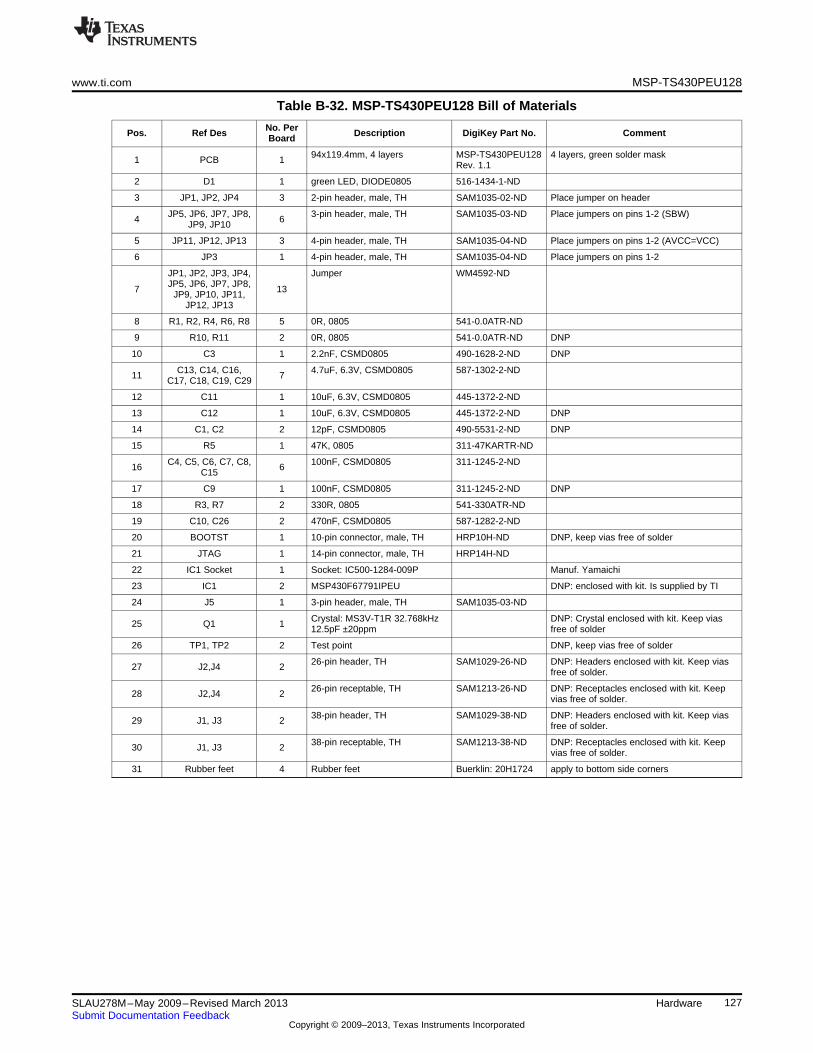
www.ti.com MSP-TS430PEU128
Table B-32. MSP-TS430PEU128 Bill of Materials
No. PerPos. Ref Des Description DigiKey Part No. CommentBoard
94x119.4mm, 4 layers MSP-TS430PEU128 4 layers, green solder mask1 PCB 1 Rev. 1.1
2 D1 1 green LED, DIODE0805 516-1434-1-ND
3 JP1, JP2, JP4 3 2-pin header, male, TH SAM1035-02-ND Place jumper on header
JP5, JP6, JP7, JP8, 3-pin header, male, TH SAM1035-03-ND Place jumpers on pins 1-2 (SBW)4 6JP9, JP10
5 JP11, JP12, JP13 3 4-pin header, male, TH SAM1035-04-ND Place jumpers on pins 1-2 (AVCC=VCC)
6 JP3 1 4-pin header, male, TH SAM1035-04-ND Place jumpers on pins 1-2
JP1, JP2, JP3, JP4, Jumper WM4592-NDJP5, JP6, JP7, JP8,7 13JP9, JP10, JP11,
JP12, JP13
8 R1, R2, R4, R6, R8 5 0R, 0805 541-0.0ATR-ND
9 R10, R11 2 0R, 0805 541-0.0ATR-ND DNP
10 C3 1 2.2nF, CSMD0805 490-1628-2-ND DNP
C13, C14, C16, 4.7uF, 6.3V, CSMD0805 587-1302-2-ND11 7C17, C18, C19, C29
12 C11 1 10uF, 6.3V, CSMD0805 445-1372-2-ND
13 C12 1 10uF, 6.3V, CSMD0805 445-1372-2-ND DNP
14 C1, C2 2 12pF, CSMD0805 490-5531-2-ND DNP
15 R5 1 47K, 0805 311-47KARTR-ND
C4, C5, C6, C7, C8, 100nF, CSMD0805 311-1245-2-ND16 6C15
17 C9 1 100nF, CSMD0805 311-1245-2-ND DNP
18 R3, R7 2 330R, 0805 541-330ATR-ND
19 C10, C26 2 470nF, CSMD0805 587-1282-2-ND
20 BOOTST 1 10-pin connector, male, TH HRP10H-ND DNP, keep vias free of solder
21 JTAG 1 14-pin connector, male, TH HRP14H-ND
22 IC1 Socket 1 Socket: IC500-1284-009P Manuf. Yamaichi
23 IC1 2 MSP430F67791IPEU DNP: enclosed with kit. Is supplied by TI
24 J5 1 3-pin header, male, TH SAM1035-03-ND
Crystal: MS3V-T1R 32.768kHz DNP: Crystal enclosed with kit. Keep vias25 Q1 1 12.5pF ±20ppm free of solder
26 TP1, TP2 2 Test point DNP, keep vias free of solder
26-pin header, TH SAM1029-26-ND DNP: Headers enclosed with kit. Keep vias27 J2,J4 2 free of solder.
26-pin receptable, TH SAM1213-26-ND DNP: Receptacles enclosed with kit. Keep28 J2,J4 2 vias free of solder.
38-pin header, TH SAM1029-38-ND DNP: Headers enclosed with kit. Keep vias29 J1, J3 2 free of solder.
38-pin receptable, TH SAM1213-38-ND DNP: Receptacles enclosed with kit. Keep30 J1, J3 2 vias free of solder.
31 Rubber feet 4 Rubber feet Buerklin: 20H1724 apply to bottom side corners
127SLAU278M–May 2009–Revised March 2013 HardwareSubmit Documentation Feedback
Copyright © 2009–2013, Texas Instruments Incorporated
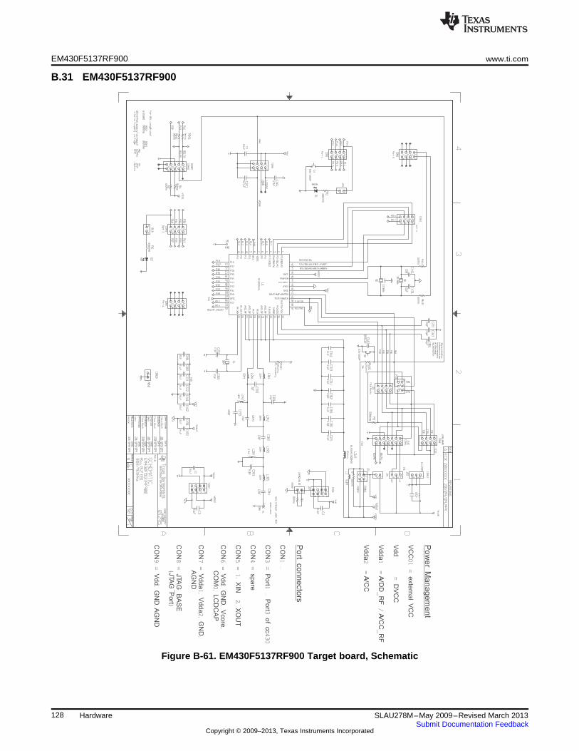
PowerManagement
VCC
exte
rnalVCC
01 =
Vdd
DVCC
=
Vdda
AVDD
RF
AVCC
RF
1 =
_/
_
Vdda
AVCC
2 =
Port
connecto
rs
CON1 ..
CON
Port
Port
ofcc
3 =
1 ..
3430
CON
spare
4 =
CON
XIN
XOUT
5 =
1:
2:
CON
Vdd
GND
Vco
re6 =
,,
,COM
LCDCAP
0,
CON
Vdda
Vdda
GND
7 =
1,
2,
,AGND
CON
JTAG
BASE
8 =
_(
)JTA
GPort
CON
Vdd
GND
AGND
9 =
,,
(Maybe
addedclose
totheres
pective
pins
toreduce
emissio
ns
at
GHztolevel
5require
dbyET
SI)
EM430F5137RF900 www.ti.com
B.31 EM430F5137RF900
Figure B-61. EM430F5137RF900 Target board, Schematic
128 Hardware SLAU278M–May 2009–Revised March 2013Submit Documentation Feedback
Copyright © 2009–2013, Texas Instruments Incorporated
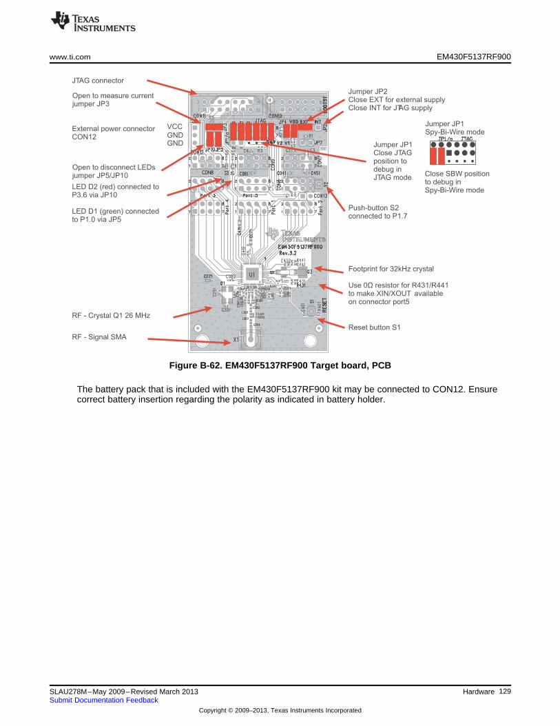
JTAG connector
External power connectorCON12
GNDGNDVCC
Open to disconnect LEDsjumper JP5/JP10
LED D2 (red) connected toP3.6 via JP10
LED D1 (green) connectedto P1.0 via JP5
RF - Crystal Q1 26 MHz
RF - Signal SMA
Reset button S1
Push-button S2connected to P1.7
Jumper JP1Close JTAGposition todebug inJTAG mode
Jumper JP2Close EXT for external supplyClose INT for JTAG supply
Close SBW positionto debug inSpy-Bi-Wire mode
Jumper JP1Spy-Bi-Wire mode
Footprint for 32kHz crystal
Use 0 resistor for R431/R441to make XIN/XOUT availableon connector port5
Ω
Open to measure currentjumper JP3
www.ti.com EM430F5137RF900
Figure B-62. EM430F5137RF900 Target board, PCB
The battery pack that is included with the EM430F5137RF900 kit may be connected to CON12. Ensurecorrect battery insertion regarding the polarity as indicated in battery holder.
129SLAU278M–May 2009–Revised March 2013 HardwareSubmit Documentation Feedback
Copyright © 2009–2013, Texas Instruments Incorporated
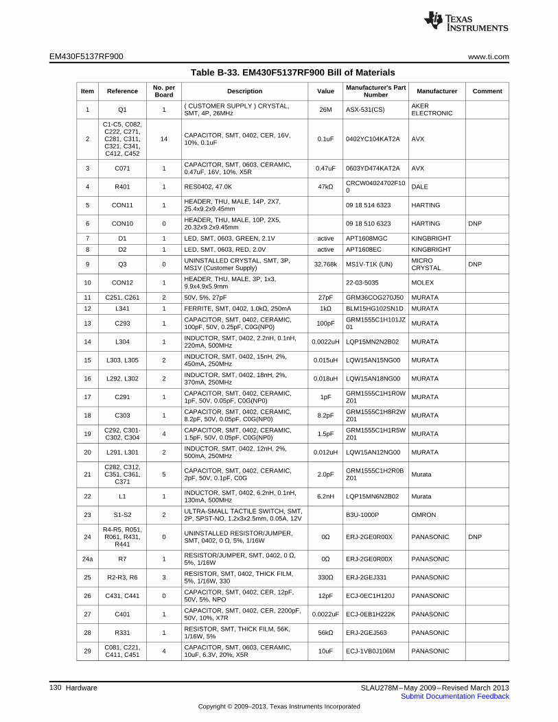
EM430F5137RF900 www.ti.com
Table B-33. EM430F5137RF900 Bill of Materials
No. per Manufacturer's PartItem Reference Description Value Manufacturer CommentBoard Number
( CUSTOMER SUPPLY ) CRYSTAL, AKER1 Q1 1 26M ASX-531(CS)SMT, 4P, 26MHz ELECTRONIC
C1-C5, C082,C222, C271, CAPACITOR, SMT, 0402, CER, 16V,2 C281, C311, 14 0.1uF 0402YC104KAT2A AVX10%, 0.1uFC321, C341,C412, C452
CAPACITOR, SMT, 0603, CERAMIC,3 C071 1 0.47uF 0603YD474KAT2A AVX0.47uF, 16V, 10%, X5R
CRCW04024702F104 R401 1 RES0402, 47.0K 47kΩ DALE0
HEADER, THU, MALE, 14P, 2X7,5 CON11 1 09 18 514 6323 HARTING25.4x9.2x9.45mm
HEADER, THU, MALE, 10P, 2X5,6 CON10 0 09 18 510 6323 HARTING DNP20.32x9.2x9.45mm
7 D1 1 LED, SMT, 0603, GREEN, 2.1V active APT1608MGC KINGBRIGHT
8 D2 1 LED, SMT, 0603, RED, 2.0V active APT1608EC KINGBRIGHT
UNINSTALLED CRYSTAL, SMT, 3P, MICRO9 Q3 0 32.768k MS1V-T1K (UN) DNPMS1V (Customer Supply) CRYSTAL
HEADER, THU, MALE, 3P, 1x3,10 CON12 1 22-03-5035 MOLEX9.9x4.9x5.9mm
11 C251, C261 2 50V, 5%, 27pF 27pF GRM36COG270J50 MURATA
12 L341 1 FERRITE, SMT, 0402, 1.0kΩ, 250mA 1kΩ BLM15HG102SN1D MURATA
CAPACITOR, SMT, 0402, CERAMIC, GRM1555C1H101JZ13 C293 1 100pF MURATA100pF, 50V, 0.25pF, C0G(NP0) 01
INDUCTOR, SMT, 0402, 2.2nH, 0.1nH,14 L304 1 0.0022uH LQP15MN2N2B02 MURATA220mA, 500MHz
INDUCTOR, SMT, 0402, 15nH, 2%,15 L303, L305 2 0.015uH LQW15AN15NG00 MURATA450mA, 250MHz
INDUCTOR, SMT, 0402, 18nH, 2%,16 L292, L302 2 0.018uH LQW15AN18NG00 MURATA370mA, 250MHz
CAPACITOR, SMT, 0402, CERAMIC, GRM1555C1H1R0W17 C291 1 1pF MURATA1pF, 50V, 0.05pF, C0G(NP0) Z01
CAPACITOR, SMT, 0402, CERAMIC, GRM1555C1H8R2W18 C303 1 8.2pF MURATA8.2pF, 50V, 0.05pF, C0G(NP0) Z01
C292, C301- CAPACITOR, SMT, 0402, CERAMIC, GRM1555C1H1R5W19 4 1.5pF MURATAC302, C304 1.5pF, 50V, 0.05pF, C0G(NP0) Z01
INDUCTOR, SMT, 0402, 12nH, 2%,20 L291, L301 2 0.012uH LQW15AN12NG00 MURATA500mA, 250MHz
C282, C312, CAPACITOR, SMT, 0402, CERAMIC, GRM1555C1H2R0B21 C351, C361, 5 2.0pF Murata2pF, 50V, 0.1pF, C0G Z01C371
INDUCTOR, SMT, 0402, 6.2nH, 0.1nH,22 L1 1 6.2nH LQP15MN6N2B02 Murata130mA, 500MHz
ULTRA-SMALL TACTILE SWITCH, SMT,23 S1-S2 2 B3U-1000P OMRON2P, SPST-NO, 1.2x3x2.5mm, 0.05A, 12V
R4-R5, R051, UNINSTALLED RESISTOR/JUMPER,24 R061, R431, 0 0Ω ERJ-2GE0R00X PANASONIC DNPSMT, 0402, 0 Ω, 5%, 1/16WR441
RESISTOR/JUMPER, SMT, 0402, 0 Ω,24a R7 1 0Ω ERJ-2GE0R00X PANASONIC5%, 1/16W
RESISTOR, SMT, 0402, THICK FILM,25 R2-R3, R6 3 330Ω ERJ-2GEJ331 PANASONIC5%, 1/16W, 330
CAPACITOR, SMT, 0402, CER, 12pF,26 C431, C441 0 12pF ECJ-0EC1H120J PANASONIC50V, 5%, NPO
CAPACITOR, SMT, 0402, CER, 2200pF,27 C401 1 0.0022uF ECJ-0EB1H222K PANASONIC50V, 10%, X7R
RESISTOR, SMT, THICK FILM, 56K,28 R331 1 56kΩ ERJ-2GEJ563 PANASONIC1/16W, 5%
C081, C221, CAPACITOR, SMT, 0603, CERAMIC,29 4 10uF ECJ-1VB0J106M PANASONICC411, C451 10uF, 6.3V, 20%, X5R
130 Hardware SLAU278M–May 2009–Revised March 2013Submit Documentation Feedback
Copyright © 2009–2013, Texas Instruments Incorporated

www.ti.com EM430F5137RF900
Table B-33. EM430F5137RF900 Bill of Materials (continued)
No. per Manufacturer's PartItem Reference Description Value Manufacturer CommentBoard Number
RESISTOR/JUMPER, SMT, 0402, 0 Ω,30 R1 1 0Ω ERJ-2GE0R00X PANASONIC5%, 1/16W
UNINSTALLED CAP CERAMIC 4.7UF31 C041 0 4.7uF ECJ-1VB0J475K Panasonic DNP6.3V X5R 0603
32 X1 1 SMA STRIGHT JACK, SMT 32K10A-40ML5 ROSENBERGER
33 Q2 0 Crystal, SMT, 32.768 kHz 32.768k MS3V-T1R Micro Crystal DNP
DUT, SMT, PQFP, RGZ-48, 0.5mmLS,34 U1 1 CC430F52x1 TI7.15x7.15x1mm, THRM.PAD
35 JP1 1 Pin Connector 2x4pin 61300821121 WUERTH
36 CON1-CON9 0 Pin Connector 2x4pin 61300821121 WUERTH DNP
37 JP2 1 Pin Connector 1x3pin 61300311121 WUERTH
JP3, JP5,38 3 Pin Connector 1x2pin 61300211121 WUERTHJP10
38a JP7, CON13 0 Pin Connector 1x2pin 61300211121 WUERTH DNP
39 JP4 1 Pin Connector 2x2pin 61300421121 WUERTH DNP
40 JP1a 1 Pin Connector 2x3pin 61300621121 WUERTH
131SLAU278M–May 2009–Revised March 2013 HardwareSubmit Documentation Feedback
Copyright © 2009–2013, Texas Instruments Incorporated
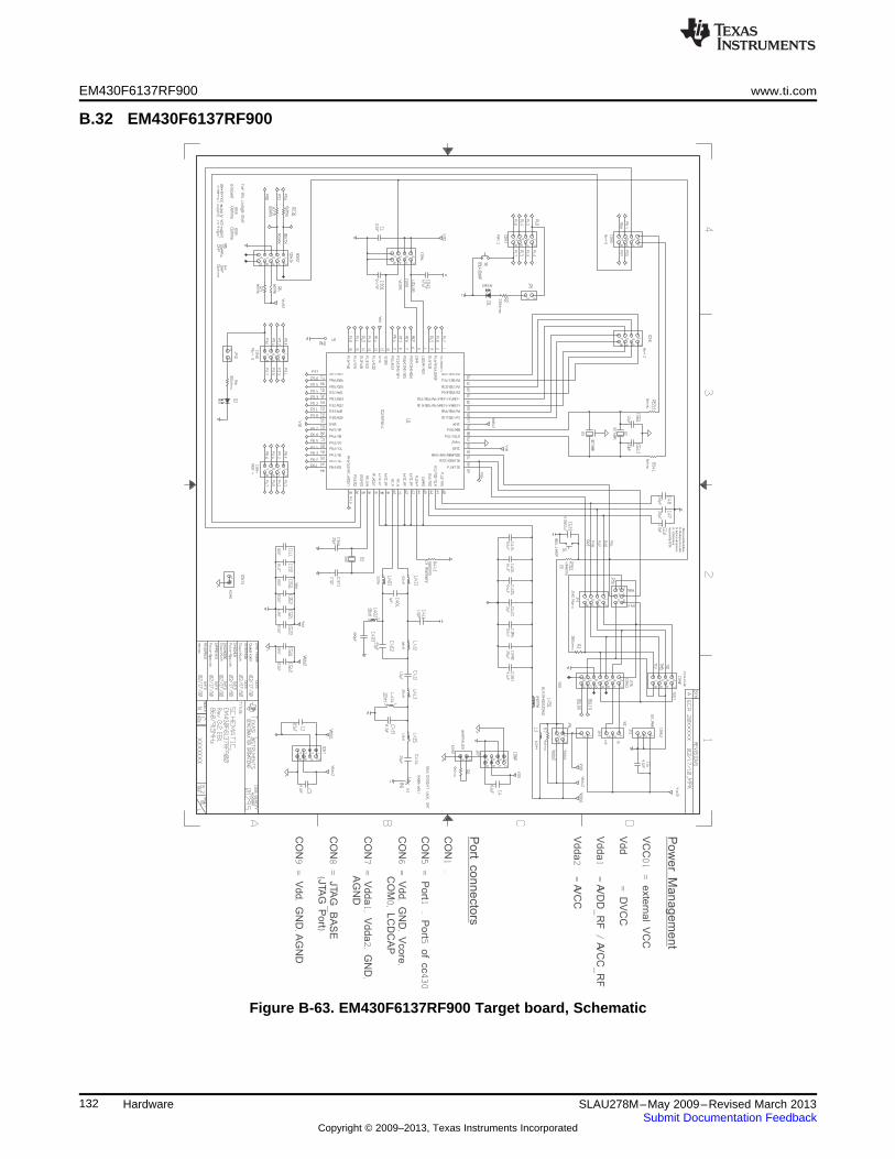
PowerManagement
VCC
exte
rnalVCC
01 =
Vdd
DVCC
=
Vdda
AVDD
RF
AVCC
RF
1 =
_/
_
Vdda
AVCC
2 =
Port
connecto
rs
CON1 ..
CON
Port
Port
ofcc
5 =
1 ..
5430
CON
Vdd
GND
Vco
re6 =
,,
,COM
LCDCAP
0,
CON
Vdda
Vdda
GND
7 =
1,
2,
,AGND
CON
JTAG
BASE
8 =
_(
)JTA
GPort
CON
Vdd
GND
AGND
9 =
,,
(Maybeaddedclose
totherespectiv
epins
toreduceem
issio
ns
at
GHz
tolev
el5
require
dby
ETSI)
EM430F6137RF900 www.ti.com
B.32 EM430F6137RF900
Figure B-63. EM430F6137RF900 Target board, Schematic
132 Hardware SLAU278M–May 2009–Revised March 2013Submit Documentation Feedback
Copyright © 2009–2013, Texas Instruments Incorporated
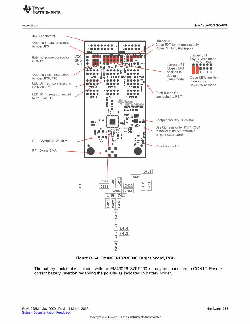
JTAG connector
External power connectorCON12
GNDGNDVCC
Open to disconnect LEDsjumper JP5/JP10
LED D2 (red) connected toP3.6 via JP10
LED D1 (green) connectedto P1.0 via JP5
RF - Crystal Q1 26 MHz
RF - Signal SMA
Reset button S1
Push-button S2connected to P1.7
Jumper JP1Close JTAGposition todebug inJTAG mode
Jumper JP2Close EXT for external supplyClose INT for JTAG supply
Close SBW positionto debug inSpy-Bi-Wire mode
Jumper JP1Spy-Bi-Wire mode
Footprint for 32kHz crystal
Use 0 resistor for R541/R551to makeP5.0/P5.1 availableon connector port5
Ω
Open to measure currentjumper JP3
C392
C422
L451
www.ti.com EM430F6137RF900
Figure B-64. EM430F6137RF900 Target board, PCB
The battery pack that is included with the EM430F6137RF900 kit may be connected to CON12. Ensurecorrect battery insertion regarding the polarity as indicated in battery holder.
133SLAU278M–May 2009–Revised March 2013 HardwareSubmit Documentation Feedback
Copyright © 2009–2013, Texas Instruments Incorporated
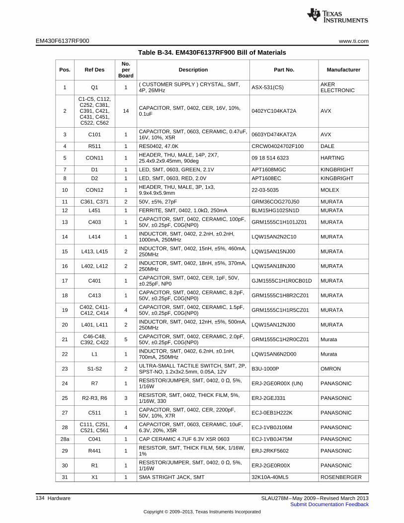
EM430F6137RF900 www.ti.com
Table B-34. EM430F6137RF900 Bill of Materials
No.Pos. Ref Des per Description Part No. Manufacturer
Board
( CUSTOMER SUPPLY ) CRYSTAL, SMT, AKER1 Q1 1 ASX-531(CS)4P, 26MHz ELECTRONIC
C1-C5, C112,C252, C381, CAPACITOR, SMT, 0402, CER, 16V, 10%,2 C391, C421, 14 0402YC104KAT2A AVX0.1uFC431, C451,C522, C562
CAPACITOR, SMT, 0603, CERAMIC, 0.47uF,3 C101 1 0603YD474KAT2A AVX16V, 10%, X5R
4 R511 1 RES0402, 47.0K CRCW04024702F100 DALE
HEADER, THU, MALE, 14P, 2X7,5 CON11 1 09 18 514 6323 HARTING25.4x9.2x9.45mm, 90deg
7 D1 1 LED, SMT, 0603, GREEN, 2.1V APT1608MGC KINGBRIGHT
8 D2 1 LED, SMT, 0603, RED, 2.0V APT1608EC KINGBRIGHT
HEADER, THU, MALE, 3P, 1x3,10 CON12 1 22-03-5035 MOLEX9.9x4.9x5.9mm
11 C361, C371 2 50V, ±5%, 27pF GRM36COG270J50 MURATA
12 L451 1 FERRITE, SMT, 0402, 1.0kΩ, 250mA BLM15HG102SN1D MURATA
CAPACITOR, SMT, 0402, CERAMIC, 100pF,13 C403 1 GRM1555C1H101JZ01 MURATA50V, ±0.25pF, C0G(NP0)
INDUCTOR, SMT, 0402, 2.2nH, ±0.2nH,14 L414 1 LQW15AN2N2C10 MURATA1000mA, 250MHz
INDUCTOR, SMT, 0402, 15nH, ±5%, 460mA,15 L413, L415 2 LQW15AN15NJ00 MURATA250MHz
INDUCTOR, SMT, 0402, 18nH, ±5%, 370mA,16 L402, L412 2 LQW15AN18NJ00 MURATA250MHz
CAPACITOR, SMT, 0402, CER, 1pF, 50V,17 C401 1 GJM1555C1H1R0CB01D MURATA±0.25pF, NP0
CAPACITOR, SMT, 0402, CERAMIC, 8.2pF,18 C413 1 GRM1555C1H8R2CZ01 MURATA50V, ±0.25pF, C0G(NP0)
C402, C411- CAPACITOR, SMT, 0402, CERAMIC, 1.5pF,19 4 GRM1555C1H1R5CZ01 MURATAC412, C414 50V, ±0.25pF, C0G(NP0)
INDUCTOR, SMT, 0402, 12nH, ±5%, 500mA,20 L401, L411 2 LQW15AN12NJ00 MURATA250MHz
C46-C48, CAPACITOR, SMT, 0402, CERAMIC, 2.0pF,21 5 GRM1555C1H2R0CZ01 MurataC392, C422 50V, ±0.25pF, C0G(NP0)
INDUCTOR, SMT, 0402, 6.2nH, ±0.1nH,22 L1 1 LQW15AN6N2D00 Murata700mA, 250MHz
ULTRA-SMALL TACTILE SWITCH, SMT, 2P,23 S1-S2 2 B3U-1000P OMRONSPST-NO, 1.2x3x2.5mm, 0.05A, 12V
RESISTOR/JUMPER, SMT, 0402, 0 Ω, 5%,24 R7 1 ERJ-2GE0R00X (UN) PANASONIC1/16W
RESISTOR, SMT, 0402, THICK FILM, 5%,25 R2-R3, R6 3 ERJ-2GEJ331 PANASONIC1/16W, 330
CAPACITOR, SMT, 0402, CER, 2200pF,27 C511 1 ECJ-0EB1H222K PANASONIC50V, 10%, X7R
C111, C251, CAPACITOR, SMT, 0603, CERAMIC, 10uF,28 4 ECJ-1VB0J106M PANASONICC521, C561 6.3V, 20%, X5R
28a C041 1 CAP CERAMIC 4.7UF 6.3V X5R 0603 ECJ-1VB0J475M PANASONIC
RESISTOR, SMT, THICK FILM, 56K, 1/16W,29 R441 1 ERJ-2RKF5602 PANASONIC1%
RESISTOR/JUMPER, SMT, 0402, 0 Ω, 5%,30 R1 1 ERJ-2GE0R00X PANASONIC1/16W
31 X1 1 SMA STRIGHT JACK, SMT 32K10A-40ML5 ROSENBERGER
134 Hardware SLAU278M–May 2009–Revised March 2013Submit Documentation Feedback
Copyright © 2009–2013, Texas Instruments Incorporated
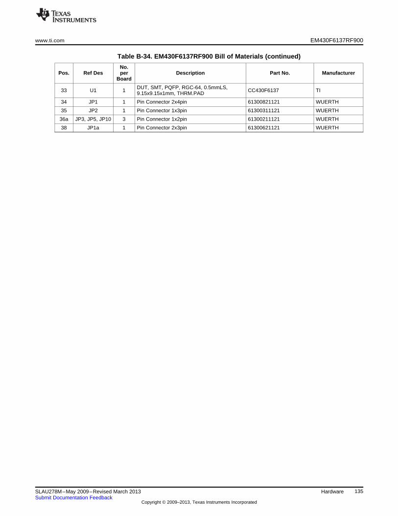
www.ti.com EM430F6137RF900
Table B-34. EM430F6137RF900 Bill of Materials (continued)
No.Pos. Ref Des per Description Part No. Manufacturer
Board
DUT, SMT, PQFP, RGC-64, 0.5mmLS,33 U1 1 CC430F6137 TI9.15x9.15x1mm, THRM.PAD
34 JP1 1 Pin Connector 2x4pin 61300821121 WUERTH
35 JP2 1 Pin Connector 1x3pin 61300311121 WUERTH
36a JP3, JP5, JP10 3 Pin Connector 1x2pin 61300211121 WUERTH
38 JP1a 1 Pin Connector 2x3pin 61300621121 WUERTH
135SLAU278M–May 2009–Revised March 2013 HardwareSubmit Documentation Feedback
Copyright © 2009–2013, Texas Instruments Incorporated
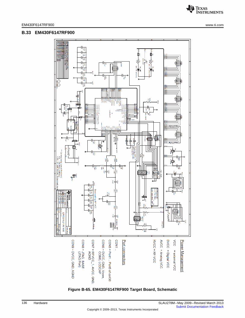
EM430F6147RF900 www.ti.com
B.33 EM430F6147RF900
Figure B-65. EM430F6147RF900 Target Board, Schematic
136 Hardware SLAU278M–May 2009–Revised March 2013Submit Documentation Feedback
Copyright © 2009–2013, Texas Instruments Incorporated

www.ti.com EM430F6147RF900
Figure B-66. EM430F6147RF900 Target Board, PCB
The battery pack which comes with the EM430F6147RF900 kit may be connected to CON12. Ensurecorrect battery insertion regarding the polarity as indicated in battery holder.
137SLAU278M–May 2009–Revised March 2013 HardwareSubmit Documentation Feedback
Copyright © 2009–2013, Texas Instruments Incorporated
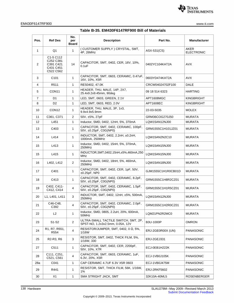
EM430F6147RF900 www.ti.com
Table B-35. EM430F6147RF900 Bill of Materials
No.Pos. Ref Des per Description Part No. Manufacturer
Board
( CUSTOMER SUPPLY ) CRYSTAL, SMT, AKER1 Q1 1 ASX-531(CS)4P, 26MHz ELECTRONIC
C1-5 C112C252 C381 CAPACITOR, SMT, 0402, CER, 16V, 10%,2 C391 C421 14 0402YC104KAT2A AVX0.1uFC431 C451C522 C562
CAPACITOR, SMT, 0603, CERAMIC, 0.47uF,3 C101 1 0603YD474KAT2A AVX16V, 10%, X5R
4 R511 1 RES0402, 47.0K CRCW04024702F100 DALE
HEADER, THU, MALE, 14P, 2X7,5 CON11 1 09 18 514 6323 HARTING25.4x9.2x9.45mm, 90deg
7 D1 1 LED, SMT, 0603, GREEN, 2.1V APT1608MGC KINGBRIGHT
8 D2 1 LED, SMT, 0603, RED, 2.0V APT1608EC KINGBRIGHT
HEADER, THU, MALE, 3P, 1x3,10 CON12 1 22-03-5035 MOLEX9.9x4.9x5.9mm
11 C361, C371 2 50V, ±5%, 27pF GRM36COG270J50 MURATA
12 L451 1 Inductor, SMD, 0402, 12nH, 5%, 370mA LQW15AN12NJ00 MURATA
CAPACITOR, SMT, 0402, CERAMIC, 100pF,13 C403 1 GRM1555C1H101JZ01 MURATA50V, ±0.25pF, C0G(NP0)
INDUCTOR, SMT, 0402, 2.2nH, ±0.2nH,14 L414 1 LQW15AN2N2C10 MURATA1000mA, 250MHz
Inductor, SMD, 0402, 15nH, 5%, 370mA,15 L413 1 LQW15AN15NJ00 MURATA250MHz
INDUCTOR,SMT,0402,15nH,±5%,460mA,25015 L415 1 LQW15AN15NJ00 MURATAMHz
Inductor, SMD, 0402, 18nH, 5%, 460mA,16 L402, L412 2 LQW15AN18NJ00 MURATA250MHz
CAPACITOR, SMT, 0402, CER, 1pF, 50V,17 C401 1 GJM1555C1H1R0CB01D MURATA±0.25pF, NP0
CAPACITOR, SMT, 0402, CERAMIC, 8.2pF,18 C413 1 GRM1555C1H8R2CZ01 MURATA50V, ±0.25pF, C0G(NP0)
C402, C411- CAPACITOR, SMT, 0402, CERAMIC, 1.5pF,19 4 GRM1555C1H1R5CZ01 MURATAC412, C414 50V, ±0.25pF, C0G(NP0)
INDUCTOR, SMT, 0402, 12nH, ±5%, 500mA,20 L1, L401, L411 3 LQW15AN12NJ00 MURATA250MHz
C46-C48, CAPACITOR, SMT, 0402, CERAMIC, 2.0pF,21 4 GRM1555C1H2R0CZ01 MURATAC392 50V, ±0.25pF, C0G(NP0)
Inductor, SMD, 0805, 2.2uH, 20%, 600mA,22 L2 1 LQM21PN2R2MC0 MURATA50MHz
ULTRA-SMALL TACTILE SWITCH, SMT, 2P,23 S1-S2 2 B3U-1000P OMRONSPST-NO, 1.2x3x2.5mm, 0.05A, 12V
R1, R7, R551, RESISTOR/JUMPER, SMT, 0402, 0 Ω, 5%,24 4 ERJ-2GE0R00X (UN) PANASONICR554 1/16W
RESISTOR, SMT, 0402, THICK FILM, 5%,25 R2-R3, R6 3 ERJ-2GEJ331 PANASONIC1/16W, 330
CAPACITOR, SMT, 0402, CER, 2200pF,27 C511 1 ECJ-0EB1H222K PANASONIC50V, 10%, X7R
C111, C251, CAPACITOR, SMT, 0603, CERAMIC, 1uF,28 4 ECJ-1VB0J105K PANASONICC521, C561 6.3V, 20%, X5R
28a C041 1 CAP CERAMIC 4.7UF 6.3V X5R 0603 ECJ-1VB0J475M PANASONIC
RESISTOR, SMT, THICK FILM, 56K, 1/16W,29 R441 1 ERJ-2RKF5602 PANASONIC1%
30 X1 1 SMA STRIGHT JACK, SMT 32K10A-40ML5 ROSENBERGER
138 Hardware SLAU278M–May 2009–Revised March 2013Submit Documentation Feedback
Copyright © 2009–2013, Texas Instruments Incorporated
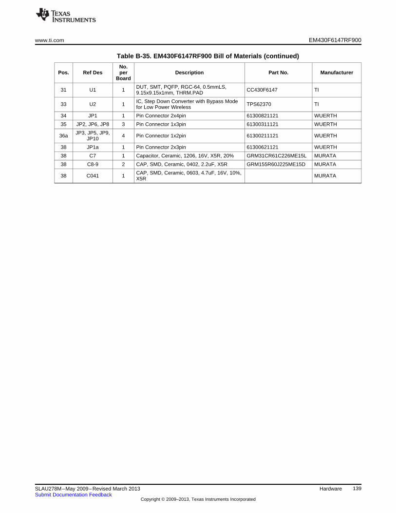
www.ti.com EM430F6147RF900
Table B-35. EM430F6147RF900 Bill of Materials (continued)
No.Pos. Ref Des per Description Part No. Manufacturer
Board
DUT, SMT, PQFP, RGC-64, 0.5mmLS,31 U1 1 CC430F6147 TI9.15x9.15x1mm, THRM.PAD
IC, Step Down Converter with Bypass Mode33 U2 1 TPS62370 TIfor Low Power Wireless
34 JP1 1 Pin Connector 2x4pin 61300821121 WUERTH
35 JP2, JP6, JP8 3 Pin Connector 1x3pin 61300311121 WUERTH
JP3, JP5, JP9,36a 4 Pin Connector 1x2pin 61300211121 WUERTHJP10
38 JP1a 1 Pin Connector 2x3pin 61300621121 WUERTH
38 C7 1 Capacitor, Ceramic, 1206, 16V, X5R, 20% GRM31CR61C226ME15L MURATA
38 C8-9 2 CAP, SMD, Ceramic, 0402, 2.2uF, X5R GRM155R60J225ME15D MURATA
CAP, SMD, Ceramic, 0603, 4.7uF, 16V, 10%,38 C041 1 MURATAX5R
139SLAU278M–May 2009–Revised March 2013 HardwareSubmit Documentation Feedback
Copyright © 2009–2013, Texas Instruments Incorporated
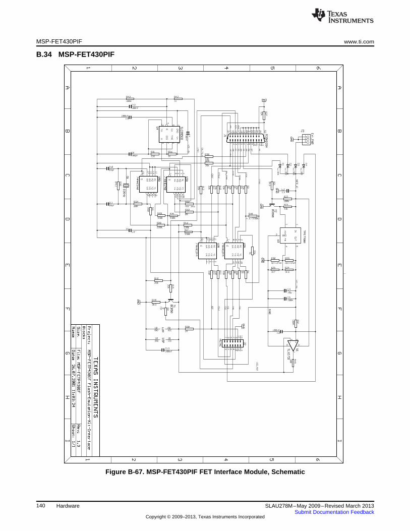
MSP-FET430PIF www.ti.com
B.34 MSP-FET430PIF
Figure B-67. MSP-FET430PIF FET Interface Module, Schematic
140 Hardware SLAU278M–May 2009–Revised March 2013Submit Documentation Feedback
Copyright © 2009–2013, Texas Instruments Incorporated
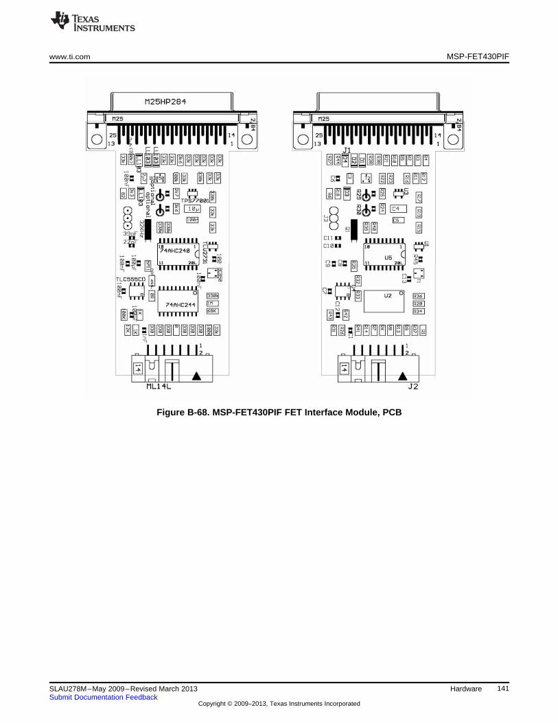
www.ti.com MSP-FET430PIF
Figure B-68. MSP-FET430PIF FET Interface Module, PCB
141SLAU278M–May 2009–Revised March 2013 HardwareSubmit Documentation Feedback
Copyright © 2009–2013, Texas Instruments Incorporated
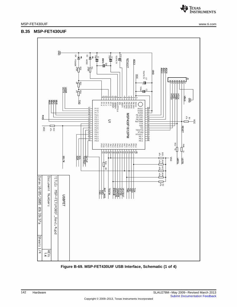
MSP-FET430UIF www.ti.com
B.35 MSP-FET430UIF
Figure B-69. MSP-FET430UIF USB Interface, Schematic (1 of 4)
142 Hardware SLAU278M–May 2009–Revised March 2013Submit Documentation Feedback
Copyright © 2009–2013, Texas Instruments Incorporated
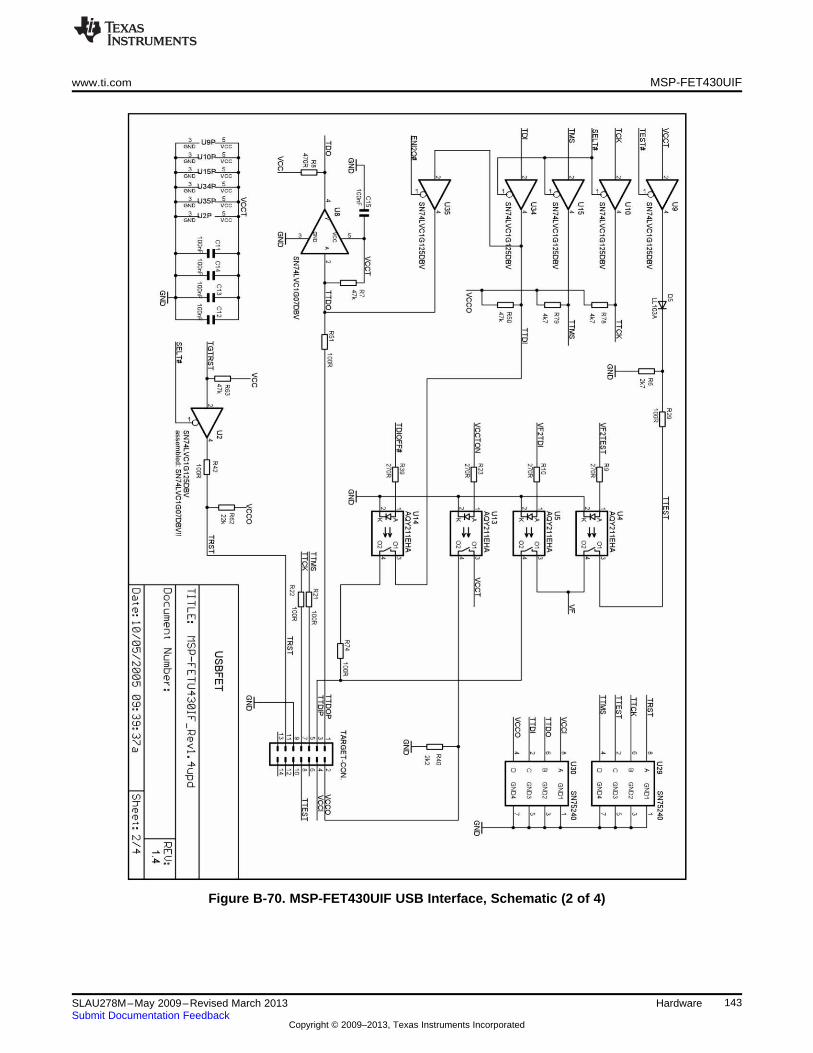
www.ti.com MSP-FET430UIF
Figure B-70. MSP-FET430UIF USB Interface, Schematic (2 of 4)
143SLAU278M–May 2009–Revised March 2013 HardwareSubmit Documentation Feedback
Copyright © 2009–2013, Texas Instruments Incorporated
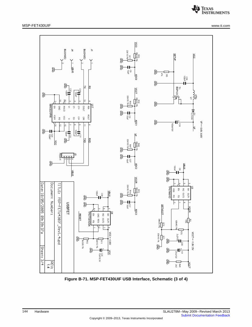
MSP-FET430UIF www.ti.com
Figure B-71. MSP-FET430UIF USB Interface, Schematic (3 of 4)
144 Hardware SLAU278M–May 2009–Revised March 2013Submit Documentation Feedback
Copyright © 2009–2013, Texas Instruments Incorporated
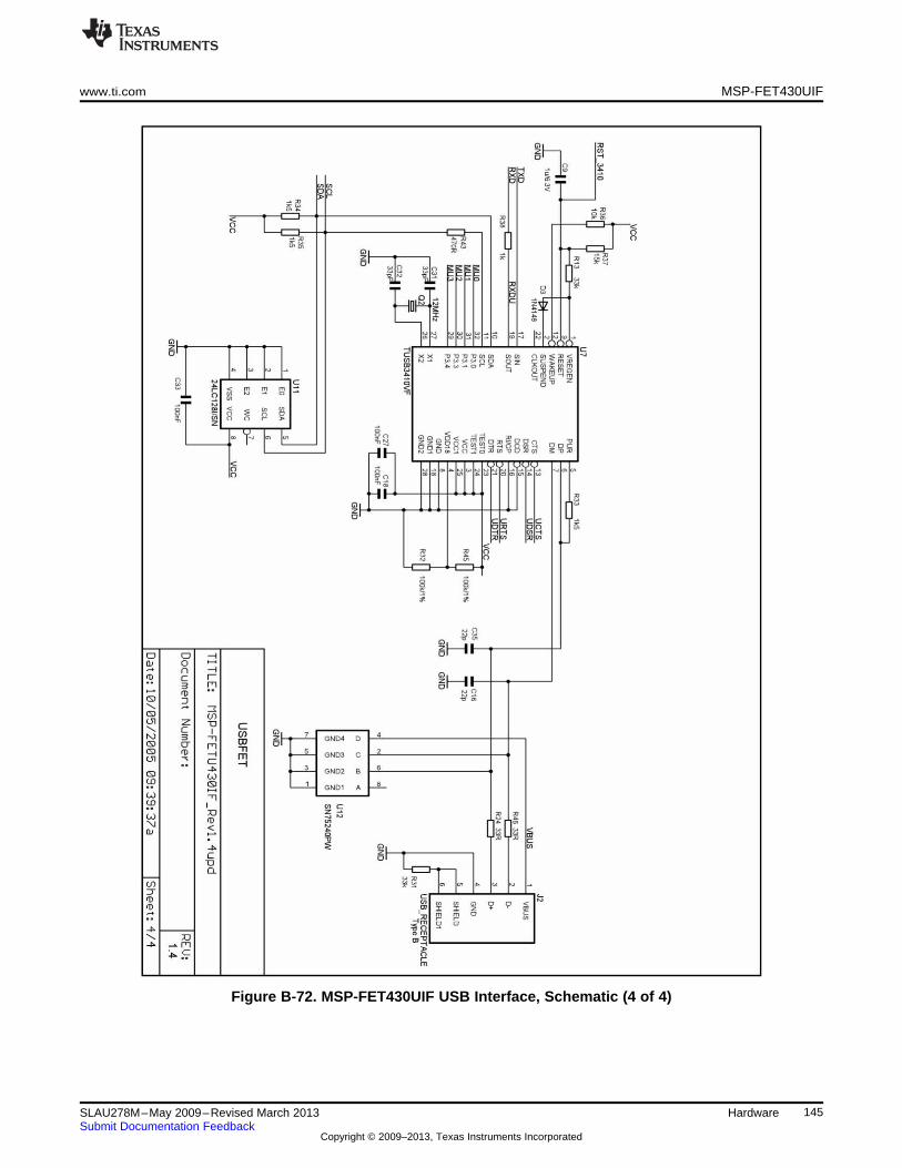
www.ti.com MSP-FET430UIF
Figure B-72. MSP-FET430UIF USB Interface, Schematic (4 of 4)
145SLAU278M–May 2009–Revised March 2013 HardwareSubmit Documentation Feedback
Copyright © 2009–2013, Texas Instruments Incorporated
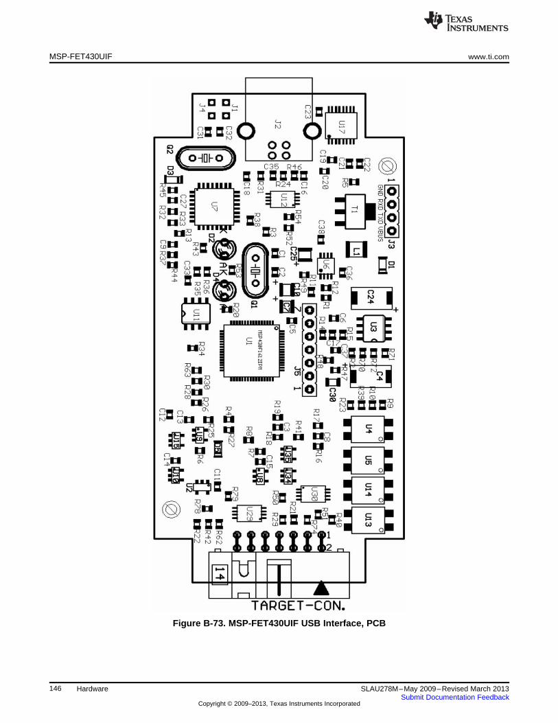
MSP-FET430UIF www.ti.com
Figure B-73. MSP-FET430UIF USB Interface, PCB
146 Hardware SLAU278M–May 2009–Revised March 2013Submit Documentation Feedback
Copyright © 2009–2013, Texas Instruments Incorporated
www.ti.com MSP-FET430UIF
B.35.1 MSP-FET430UIF Revision History
Revision 1.3
• Initial released hardware version
Assembly change on 1.3 (May 2005)
• R29, R51, R42, R21, R22, R74: value changed from 330R to 100R
Changes 1.3 to 1.4 (Aug 2005)
• J5: VBUS and RESET additionally connected
• R29, R51, R42, R21, R22, R74: value changed from 330R to 100R
• U1, U7: F1612 can reset TUSB3410; R44 = 0R added
• TARGET-CON.: pins 6, 10, 12, 13, 14 disconnected from GND
• Firmware-upgrade option through BSL: R49, R52, R53, R54 added; R49, R52 are currently DNP
• Pullups on TCK and TMS: R78, R79 added
• U2: Changed from SN74LVC1G125DBV to SN74LVC1G07DBV
NOTE: Using a locally powered target board with hardware revision 1.4
Using an MSP-FET430UIF interface hardware revision 1.4 with populated R62 in conjunctionwith a locally powered target board is not possible. In this case, the target device RESETsignal is pulled down by the FET tool. It is recommended to remove R62 to eliminate thisrestriction. This component is located close to the 14-pin connector on the MSP-FET430UIFPCB. See the schematic and PCB drawings in this document for the exact location of thiscomponent.
Assembly change on 1.4 (January 2006)
• R62: not populated
147SLAU278M–May 2009–Revised March 2013 HardwareSubmit Documentation Feedback
Copyright © 2009–2013, Texas Instruments Incorporated
Appendix CSLAU278M–May 2009–Revised March 2013
Hardware Installation Guide
This section describes the hardware installation process of the following USB debug interfaces on a PCrunning Windows XP:
• MSP-FET430UIF
• eZ430-F2013
• eZ430-RF2500
• eZ430-Chronos
• eZ430-RF2780
• eZ430-RF2560
• MSP-WDSxx "Metawatch"
• LaunchPad (MSP-EXP430G2)
• MSP-EXP430FR5739
• MSP-EXP430F5529
The installation procedure for other supported versions of Windows is very similar and, therefore, notshown here.
Topic ........................................................................................................................... Page
C.1 Hardware Installation ....................................................................................... 149
148 Hardware Installation Guide SLAU278M–May 2009–Revised March 2013Submit Documentation Feedback
Copyright © 2009–2013, Texas Instruments Incorporated
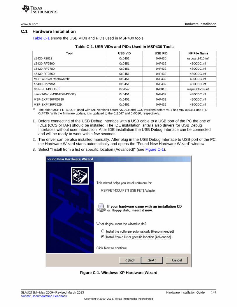
www.ti.com Hardware Installation
C.1 Hardware Installation
Table C-1 shows the USB VIDs and PIDs used in MSP430 tools.
Table C-1. USB VIDs and PIDs Used in MSP430 Tools
Tool USB VID USB PID INF File Name
eZ430-F2013 0x0451 0xF430 usbuart3410.inf
eZ430-RF2500 0x0451 0xF432 430CDC.inf
eZ430-RF2780 0x0451 0xF432 430CDC.inf
eZ430-RF2560 0x0451 0xF432 430CDC.inf
MSP-WDSxx "Metawatch" 0x0451 0xF432 430CDC.inf
eZ430-Chronos 0x0451 0xF432 430CDC.inf
MSP-FET430UIF (1) 0x2047 0x0010 msp430tools.inf
LaunchPad (MSP-EXP430G2) 0x0451 0xF432 430CDC.inf
MSP-EXP430FR5739 0x0451 0xF432 430CDC.inf
MSP-EXP430F5529 0x0451 0xF432 430CDC.inf(1) The older MSP-FET430UIF used with IAR versions before v5.20.x and CCS versions before v5.1 has VID 0x0451 and PID
0xF430. With the firmware update, it is updated to the 0x2047 and 0x0010, respectively.
1. Before connecting of the USB Debug Interface with a USB cable to a USB port of the PC the one ofIDEs (CCS or IAR) should be installed. The IDE installation isntalls also drivers for USB DebugInterfaces without user interaction. After IDE installation the USB Debug Interface can be connectedand will be ready to work within few seconds.
2. The driver can be also installed manually. After plug in the USB Debug Interface to USB port of the PCthe Hardware Wizard starts automatically and opens the "Found New Hardware Wizard" window.
3. Select "Install from a list or specific location (Advanced)" (see Figure C-1).
Figure C-1. Windows XP Hardware Wizard
149SLAU278M–May 2009–Revised March 2013 Hardware Installation GuideSubmit Documentation Feedback
Copyright © 2009–2013, Texas Instruments Incorporated
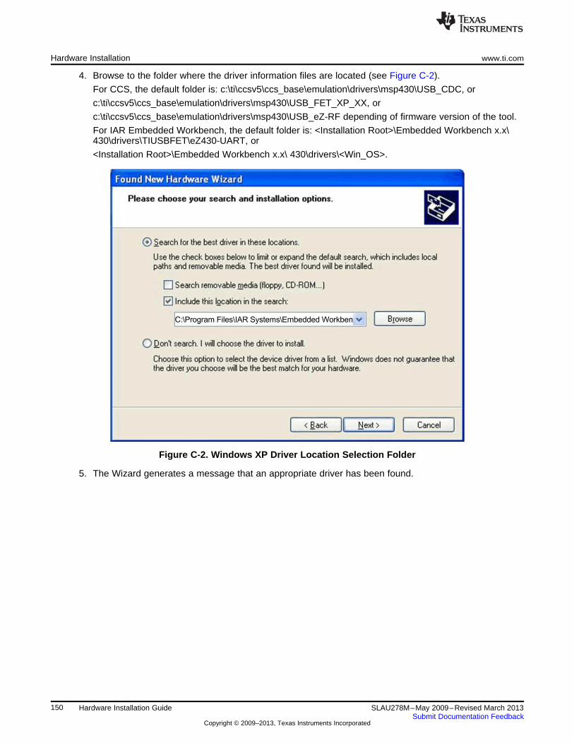
Hardware Installation www.ti.com
4. Browse to the folder where the driver information files are located (see Figure C-2).
For CCS, the default folder is: c:\ti\ccsv5\ccs_base\emulation\drivers\msp430\USB_CDC, or
c:\ti\ccsv5\ccs_base\emulation\drivers\msp430\USB_FET_XP_XX, or
c:\ti\ccsv5\ccs_base\emulation\drivers\msp430\USB_eZ-RF depending of firmware version of the tool.
For IAR Embedded Workbench, the default folder is: <Installation Root>\Embedded Workbench x.x\430\drivers\TIUSBFET\eZ430-UART, or
<Installation Root>\Embedded Workbench x.x\ 430\drivers\<Win_OS>.
Figure C-2. Windows XP Driver Location Selection Folder
5. The Wizard generates a message that an appropriate driver has been found.
150 Hardware Installation Guide SLAU278M–May 2009–Revised March 2013Submit Documentation Feedback
Copyright © 2009–2013, Texas Instruments Incorporated
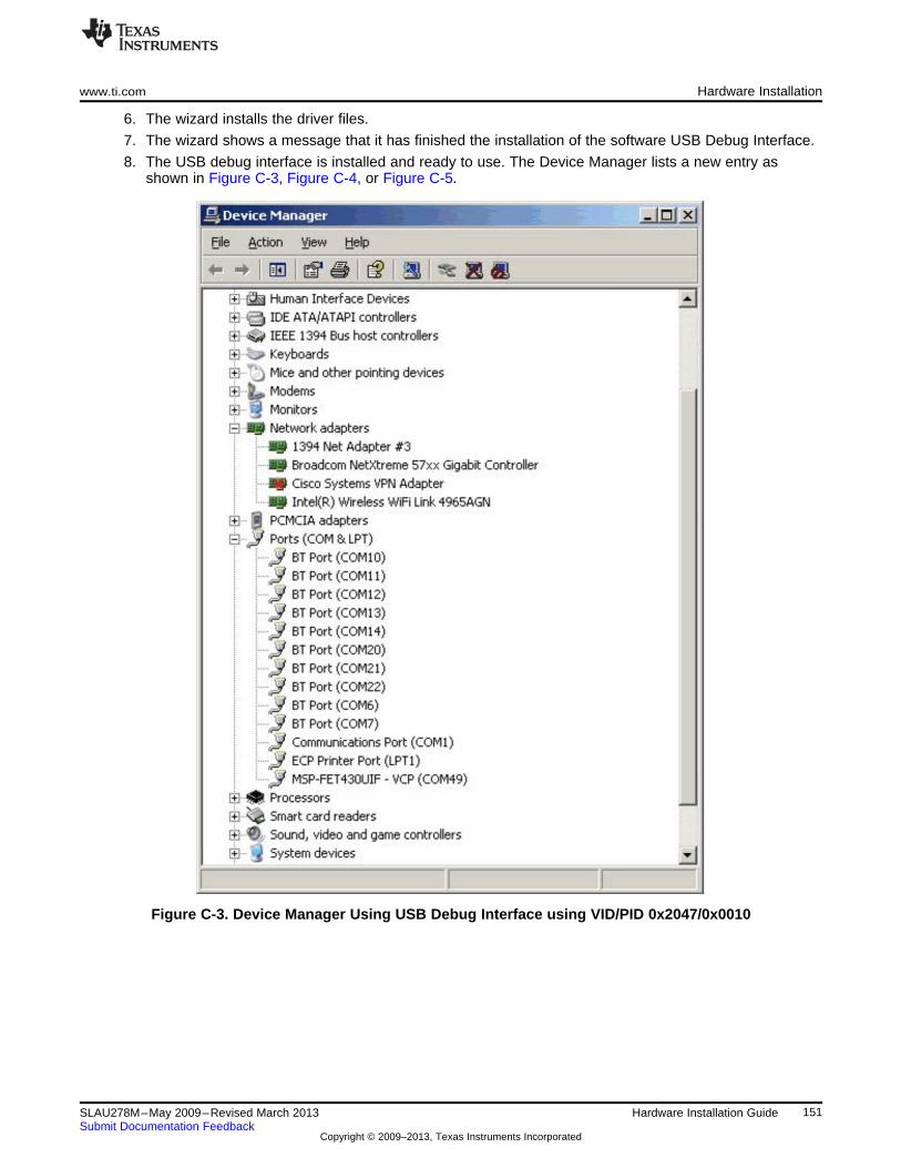
www.ti.com Hardware Installation
6. The wizard installs the driver files.
7. The wizard shows a message that it has finished the installation of the software USB Debug Interface.
8. The USB debug interface is installed and ready to use. The Device Manager lists a new entry asshown in Figure C-3, Figure C-4, or Figure C-5.
Figure C-3. Device Manager Using USB Debug Interface using VID/PID 0x2047/0x0010
151SLAU278M–May 2009–Revised March 2013 Hardware Installation GuideSubmit Documentation Feedback
Copyright © 2009–2013, Texas Instruments Incorporated
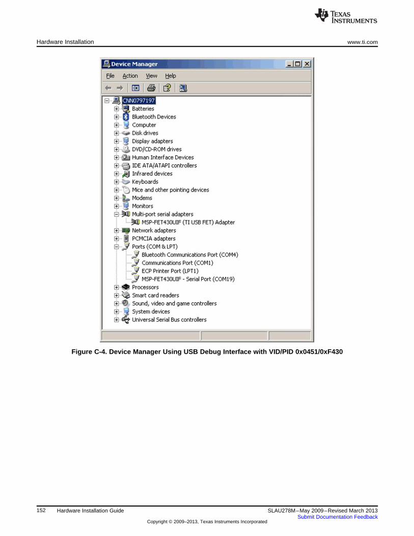
Hardware Installation www.ti.com
Figure C-4. Device Manager Using USB Debug Interface with VID/PID 0x0451/0xF430
152 Hardware Installation Guide SLAU278M–May 2009–Revised March 2013Submit Documentation Feedback
Copyright © 2009–2013, Texas Instruments Incorporated
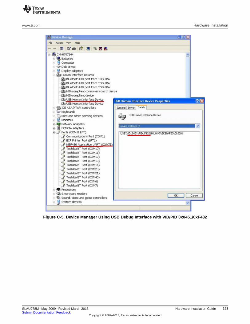
www.ti.com Hardware Installation
Figure C-5. Device Manager Using USB Debug Interface with VID/PID 0x0451/0xF432
153SLAU278M–May 2009–Revised March 2013 Hardware Installation GuideSubmit Documentation Feedback
Copyright © 2009–2013, Texas Instruments Incorporated
Document Revision History www.ti.com
Document Revision HistoryVersion Changes
SLAU278 Initial release
SLAU278A Updated USB driver installation according to CCE v3.1 SR1 and CCS v4.
SLAU278B Added information about MSP-FET430U80USB, MSP-TS430PN80USB, and eZ430-Chronos.
Added bills of materials and updated some PCBs in Appendix B.SLAU278CAdded information about MSP-TS430DA38, MSP-TS430DL48, MSP-TS430PW14, MSP-TS430PW28.
Added information about MSP-TS430L092, MSP-TS430RSB40, MSP-TS430RGC64USB, MSP-TS430PZ100USB, MSP-SLAU278DFET430F5137RF900
Added jumper information for MSP-TS430L092 PCBs to Appendix B.SLAU278EAdded new supported devices in Chapter 1.
Added information about MSP-TS430PW24, MSP-TS430PW28A, MSP-TS430RHA40A, MSP-TS430RGZ48B, MSP-SLAU278F TS430RGC64B, MSP-TS430PN80A, and MSP-TS430PZ100B.
Updated MSP-TS430RSB40 schematics
SLAU278G Added information for MSP-TS430PZ100C
SLAU278H Added information for MSP-TS430D8 and MSP-TS430RGC64C
Updated Table 1-1.Replaced Figure 2-2.Added Figure 2-3.SLAU278IReplaced Figure B-37 and Figure B-67.Added Table C-1.Editorial changes throughout.
SLAU278J Added EM430F6147RF900 Section B.33.
Added battery pack connection information to all EM430Fx1x7RF900 kits.SLAU278K Added information for MSP-TS430RGZ48C and MSP-TS430PEU128.
Updated Figure B-38.
Changed descriptions in Section B.19 and Section B.30.SLAU278LChanged Figure B-60.
SLAU278M Added information for MSP430G2x44 and MSP430G2x55 in Table 1-2.
NOTE: Page numbers for previous revisions may differ from page numbers in the current version.
154 Revision History SLAU278M–May 2009–Revised March 2013Submit Documentation Feedback
Copyright © 2009–2013, Texas Instruments Incorporated

RF EMISSION TESTING
All MSP-TS430xxx kits and kits listed below have been tested for compliance with Part 15 of the FCC and Canadian ICES-003 rules. SeeREGULATORY COMPLIANCE INFORMATION for details on compliance with these rules. All other kits described in this document eitherhave not been tested or have the statement in their documentation, which is listed in Related Documentation From Texas Instruments.
MSP-FET430UIF

EVALUATION BOARD/KIT/MODULE (EVM) ADDITIONAL TERMS
Texas Instruments (TI) provides the enclosed Evaluation Board/Kit/Module (EVM) under the following conditions:
The user assumes all responsibility and liability for proper and safe handling of the goods. Further, the user indemnifies TI from all claimsarising from the handling or use of the goods.
Should this evaluation board/kit not meet the specifications indicated in the User’s Guide, the board/kit may be returned within 30 days fromthe date of delivery for a full refund. THE FOREGOING LIMITED WARRANTY IS THE EXCLUSIVE WARRANTY MADE BY SELLER TOBUYER AND IS IN LIEU OF ALL OTHER WARRANTIES, EXPRESSED, IMPLIED, OR STATUTORY, INCLUDING ANY WARRANTY OFMERCHANTABILITY OR FITNESS FOR ANY PARTICULAR PURPOSE. EXCEPT TO THE EXTENT OF THE INDEMNITY SET FORTHABOVE, NEITHER PARTY SHALL BE LIABLE TO THE OTHER FOR ANY INDIRECT, SPECIAL, INCIDENTAL, OR CONSEQUENTIALDAMAGES.
Please read the User's Guide and, specifically, the Warnings and Restrictions notice in the User's Guide prior to handling the product. Thisnotice contains important safety information about temperatures and voltages. For additional information on TI's environmental and/or safetyprograms, please visit www.ti.com/esh or contact TI.
No license is granted under any patent right or other intellectual property right of TI covering or relating to any machine, process, orcombination in which such TI products or services might be or are used. TI currently deals with a variety of customers for products, andtherefore our arrangement with the user is not exclusive. TI assumes no liability for applications assistance, customer product design,software performance, or infringement of patents or services described herein.
REGULATORY COMPLIANCE INFORMATION
As noted in the EVM User’s Guide and/or EVM itself, this EVM and/or accompanying hardware may or may not be subject to the FederalCommunications Commission (FCC) and Industry Canada (IC) rules.
For EVMs not subject to the above rules, this evaluation board/kit/module is intended for use for ENGINEERING DEVELOPMENT,DEMONSTRATION OR EVALUATION PURPOSES ONLY and is not considered by TI to be a finished end product fit for general consumeruse. It generates, uses, and can radiate radio frequency energy and has not been tested for compliance with the limits of computingdevices pursuant to part 15 of FCC or ICES-003 rules, which are designed to provide reasonable protection against radio frequencyinterference. Operation of the equipment may cause interference with radio communications, in which case the user at his own expense willbe required to take whatever measures may be required to correct this interference.
General Statement for EVMs including a radio
User Power/Frequency Use Obligations: This radio is intended for development/professional use only in legally allocated frequency andpower limits. Any use of radio frequencies and/or power availability of this EVM and its development application(s) must comply with locallaws governing radio spectrum allocation and power limits for this evaluation module. It is the user’s sole responsibility to only operate thisradio in legally acceptable frequency space and within legally mandated power limitations. Any exceptions to this are strictly prohibited andunauthorized by Texas Instruments unless user has obtained appropriate experimental/development licenses from local regulatoryauthorities, which is responsibility of user including its acceptable authorization.
For EVMs annotated as FCC – FEDERAL COMMUNICATIONS COMMISSION Part 15 Compliant
Caution
This device complies with part 15 of the FCC Rules. Operation is subject to the following two conditions: (1) This device may not causeharmful interference, and (2) this device must accept any interference received, including interference that may cause undesired operation.
Changes or modifications not expressly approved by the party responsible for compliance could void the user's authority to operate theequipment.
FCC Interference Statement for Class A EVM devices
This equipment has been tested and found to comply with the limits for a Class A digital device, pursuant to part 15 of the FCC Rules.These limits are designed to provide reasonable protection against harmful interference when the equipment is operated in a commercialenvironment. This equipment generates, uses, and can radiate radio frequency energy and, if not installed and used in accordance with theinstruction manual, may cause harmful interference to radio communications. Operation of this equipment in a residential area is likely tocause harmful interference in which case the user will be required to correct the interference at his own expense.
FCC Interference Statement for Class B EVM devices
This equipment has been tested and found to comply with the limits for a Class B digital device, pursuant to part 15 of the FCC Rules.These limits are designed to provide reasonable protection against harmful interference in a residential installation. This equipmentgenerates, uses and can radiate radio frequency energy and, if not installed and used in accordance with the instructions, may causeharmful interference to radio communications. However, there is no guarantee that interference will not occur in a particular installation. Ifthis equipment does cause harmful interference to radio or television reception, which can be determined by turning the equipment off andon, the user is encouraged to try to correct the interference by one or more of the following measures:
• Reorient or relocate the receiving antenna.• Increase the separation between the equipment and receiver.• Connect the equipment into an outlet on a circuit different from that to which the receiver is connected.• Consult the dealer or an experienced radio/TV technician for help.
For EVMs annotated as IC – INDUSTRY CANADA Compliant
This Class A or B digital apparatus complies with Canadian ICES-003.
Changes or modifications not expressly approved by the party responsible for compliance could void the user’s authority to operate theequipment.
Concerning EVMs including radio transmitters
This device complies with Industry Canada licence-exempt RSS standard(s). Operation is subject to the following two conditions: (1) thisdevice may not cause interference, and (2) this device must accept any interference, including interference that may cause undesiredoperation of the device.
Concerning EVMs including detachable antennas
Under Industry Canada regulations, this radio transmitter may only operate using an antenna of a type and maximum (or lesser) gainapproved for the transmitter by Industry Canada. To reduce potential radio interference to other users, the antenna type and its gain shouldbe so chosen that the equivalent isotropically radiated power (e.i.r.p.) is not more than that necessary for successful communication.
This radio transmitter has been approved by Industry Canada to operate with the antenna types listed in the user guide with the maximumpermissible gain and required antenna impedance for each antenna type indicated. Antenna types not included in this list, having a gaingreater than the maximum gain indicated for that type, are strictly prohibited for use with this device.
Cet appareil numérique de la classe A ou B est conforme à la norme NMB-003 du Canada.
Les changements ou les modifications pas expressément approuvés par la partie responsable de la conformité ont pu vider l’autorité del'utilisateur pour actionner l'équipement.
Concernant les EVMs avec appareils radio
Le présent appareil est conforme aux CNR d'Industrie Canada applicables aux appareils radio exempts de licence. L'exploitation estautorisée aux deux conditions suivantes : (1) l'appareil ne doit pas produire de brouillage, et (2) l'utilisateur de l'appareil doit accepter toutbrouillage radioélectrique subi, même si le brouillage est susceptible d'en compromettre le fonctionnement.
Concernant les EVMs avec antennes détachables
Conformément à la réglementation d'Industrie Canada, le présent émetteur radio peut fonctionner avec une antenne d'un type et d'un gainmaximal (ou inférieur) approuvé pour l'émetteur par Industrie Canada. Dans le but de réduire les risques de brouillage radioélectrique àl'intention des autres utilisateurs, il faut choisir le type d'antenne et son gain de sorte que la puissance isotrope rayonnée équivalente(p.i.r.e.) ne dépasse pas l'intensité nécessaire à l'établissement d'une communication satisfaisante.
Le présent émetteur radio a été approuvé par Industrie Canada pour fonctionner avec les types d'antenne énumérés dans le manueld’usage et ayant un gain admissible maximal et l'impédance requise pour chaque type d'antenne. Les types d'antenne non inclus danscette liste, ou dont le gain est supérieur au gain maximal indiqué, sont strictement interdits pour l'exploitation de l'émetteur.
SPACER
SPACER
SPACER
SPACER
SPACER
SPACER
SPACER
SPACER
【【Important Notice for Users of this Product in Japan】】This development kit is NOT certified as Confirming to Technical Regulations of Radio Law of Japan
If you use this product in Japan, you are required by Radio Law of Japan to follow the instructions below with respect to this product:
1. Use this product in a shielded room or any other test facility as defined in the notification #173 issued by Ministry of Internal Affairs andCommunications on March 28, 2006, based on Sub-section 1.1 of Article 6 of the Ministry’s Rule for Enforcement of Radio Law ofJapan,
2. Use this product only after you obtained the license of Test Radio Station as provided in Radio Law of Japan with respect to thisproduct, or
3. Use of this product only after you obtained the Technical Regulations Conformity Certification as provided in Radio Law of Japan withrespect to this product. Also, please do not transfer this product, unless you give the same notice above to the transferee. Please notethat if you could not follow the instructions above, you will be subject to penalties of Radio Law of Japan.
Texas Instruments Japan Limited(address) 24-1, Nishi-Shinjuku 6 chome, Shinjuku-ku, Tokyo, Japan
http://www.tij.co.jp
【ご使用にあたっての注】
本開発キットは技術基準適合証明を受けておりません。
本製品のご使用に際しては、電波法遵守のため、以下のいずれかの措置を取っていただく必要がありますのでご注意ください。1. 電波法施行規則第6条第1項第1号に基づく平成18年3月28日総務省告示第173号で定められた電波暗室等の試験設備でご使用いただく。2. 実験局の免許を取得後ご使用いただく。3. 技術基準適合証明を取得後ご使用いただく。
なお、本製品は、上記の「ご使用にあたっての注意」を譲渡先、移転先に通知しない限り、譲渡、移転できないものとします。
上記を遵守頂けない場合は、電波法の罰則が適用される可能性があることをご留意ください。
日本テキサス・インスツルメンツ株式会社東京都新宿区西新宿6丁目24番1号西新宿三井ビルhttp://www.tij.co.jp
SPACER
SPACER
SPACER
SPACER
SPACER
SPACER
SPACER
SPACER
SPACER
SPACER
SPACER
SPACER
SPACER
SPACER
SPACER
SPACER
SPACER

EVALUATION BOARD/KIT/MODULE (EVM)WARNINGS, RESTRICTIONS AND DISCLAIMERS
For Feasibility Evaluation Only, in Laboratory/Development Environments. Unless otherwise indicated, this EVM is not a finishedelectrical equipment and not intended for consumer use. It is intended solely for use for preliminary feasibility evaluation inlaboratory/development environments by technically qualified electronics experts who are familiar with the dangers and application risksassociated with handling electrical mechanical components, systems and subsystems. It should not be used as all or part of a finished endproduct.
Your Sole Responsibility and Risk. You acknowledge, represent and agree that:
1. You have unique knowledge concerning Federal, State and local regulatory requirements (including but not limited to Food and DrugAdministration regulations, if applicable) which relate to your products and which relate to your use (and/or that of your employees,affiliates, contractors or designees) of the EVM for evaluation, testing and other purposes.
2. You have full and exclusive responsibility to assure the safety and compliance of your products with all such laws and other applicableregulatory requirements, and also to assure the safety of any activities to be conducted by you and/or your employees, affiliates,contractors or designees, using the EVM. Further, you are responsible to assure that any interfaces (electronic and/or mechanical)between the EVM and any human body are designed with suitable isolation and means to safely limit accessible leakage currents tominimize the risk of electrical shock hazard.
3. You will employ reasonable safeguards to ensure that your use of the EVM will not result in any property damage, injury or death, evenif the EVM should fail to perform as described or expected.
4. You will take care of proper disposal and recycling of the EVM’s electronic components and packing materials.
Certain Instructions. It is important to operate this EVM within TI’s recommended specifications and environmental considerations per theuser guidelines. Exceeding the specified EVM ratings (including but not limited to input and output voltage, current, power, andenvironmental ranges) may cause property damage, personal injury or death. If there are questions concerning these ratings please contacta TI field representative prior to connecting interface electronics including input power and intended loads. Any loads applied outside of thespecified output range may result in unintended and/or inaccurate operation and/or possible permanent damage to the EVM and/orinterface electronics. Please consult the EVM User's Guide prior to connecting any load to the EVM output. If there is uncertainty as to theload specification, please contact a TI field representative. During normal operation, some circuit components may have case temperaturesgreater than 60°C as long as the input and output are maintained at a normal ambient operating temperature. These components includebut are not limited to linear regulators, switching transistors, pass transistors, and current sense resistors which can be identified using theEVM schematic located in the EVM User's Guide. When placing measurement probes near these devices during normal operation, pleasebe aware that these devices may be very warm to the touch. As with all electronic evaluation tools, only qualified personnel knowledgeablein electronic measurement and diagnostics normally found in development environments should use these EVMs.
Agreement to Defend, Indemnify and Hold Harmless. You agree to defend, indemnify and hold TI, its licensors and their representativesharmless from and against any and all claims, damages, losses, expenses, costs and liabilities (collectively, "Claims") arising out of or inconnection with any use of the EVM that is not in accordance with the terms of the agreement. This obligation shall apply whether Claimsarise under law of tort or contract or any other legal theory, and even if the EVM fails to perform as described or expected.
Safety-Critical or Life-Critical Applications. If you intend to evaluate the components for possible use in safety critical applications (suchas life support) where a failure of the TI product would reasonably be expected to cause severe personal injury or death, such as deviceswhich are classified as FDA Class III or similar classification, then you must specifically notify TI of such intent and enter into a separateAssurance and Indemnity Agreement.
Mailing Address: Texas Instruments, Post Office Box 655303, Dallas, Texas 75265Copyright © 2013, Texas Instruments Incorporated

IMPORTANT NOTICE
Texas Instruments Incorporated and its subsidiaries (TI) reserve the right to make corrections, enhancements, improvements and otherchanges to its semiconductor products and services per JESD46, latest issue, and to discontinue any product or service per JESD48, latestissue. Buyers should obtain the latest relevant information before placing orders and should verify that such information is current andcomplete. All semiconductor products (also referred to herein as “components”) are sold subject to TI’s terms and conditions of salesupplied at the time of order acknowledgment.
TI warrants performance of its components to the specifications applicable at the time of sale, in accordance with the warranty in TI’s termsand conditions of sale of semiconductor products. Testing and other quality control techniques are used to the extent TI deems necessaryto support this warranty. Except where mandated by applicable law, testing of all parameters of each component is not necessarilyperformed.
TI assumes no liability for applications assistance or the design of Buyers’ products. Buyers are responsible for their products andapplications using TI components. To minimize the risks associated with Buyers’ products and applications, Buyers should provideadequate design and operating safeguards.
TI does not warrant or represent that any license, either express or implied, is granted under any patent right, copyright, mask work right, orother intellectual property right relating to any combination, machine, or process in which TI components or services are used. Informationpublished by TI regarding third-party products or services does not constitute a license to use such products or services or a warranty orendorsement thereof. Use of such information may require a license from a third party under the patents or other intellectual property of thethird party, or a license from TI under the patents or other intellectual property of TI.
Reproduction of significant portions of TI information in TI data books or data sheets is permissible only if reproduction is without alterationand is accompanied by all associated warranties, conditions, limitations, and notices. TI is not responsible or liable for such altereddocumentation. Information of third parties may be subject to additional restrictions.
Resale of TI components or services with statements different from or beyond the parameters stated by TI for that component or servicevoids all express and any implied warranties for the associated TI component or service and is an unfair and deceptive business practice.TI is not responsible or liable for any such statements.
Buyer acknowledges and agrees that it is solely responsible for compliance with all legal, regulatory and safety-related requirementsconcerning its products, and any use of TI components in its applications, notwithstanding any applications-related information or supportthat may be provided by TI. Buyer represents and agrees that it has all the necessary expertise to create and implement safeguards whichanticipate dangerous consequences of failures, monitor failures and their consequences, lessen the likelihood of failures that might causeharm and take appropriate remedial actions. Buyer will fully indemnify TI and its representatives against any damages arising out of the useof any TI components in safety-critical applications.
In some cases, TI components may be promoted specifically to facilitate safety-related applications. With such components, TI’s goal is tohelp enable customers to design and create their own end-product solutions that meet applicable functional safety standards andrequirements. Nonetheless, such components are subject to these terms.
No TI components are authorized for use in FDA Class III (or similar life-critical medical equipment) unless authorized officers of the partieshave executed a special agreement specifically governing such use.
Only those TI components which TI has specifically designated as military grade or “enhanced plastic” are designed and intended for use inmilitary/aerospace applications or environments. Buyer acknowledges and agrees that any military or aerospace use of TI componentswhich have not been so designated is solely at the Buyer's risk, and that Buyer is solely responsible for compliance with all legal andregulatory requirements in connection with such use.
TI has specifically designated certain components as meeting ISO/TS16949 requirements, mainly for automotive use. In any case of use ofnon-designated products, TI will not be responsible for any failure to meet ISO/TS16949.
Products Applications
Audio www.ti.com/audio Automotive and Transportation www.ti.com/automotive
Amplifiers amplifier.ti.com Communications and Telecom www.ti.com/communications
Data Converters dataconverter.ti.com Computers and Peripherals www.ti.com/computers
DLP® Products www.dlp.com Consumer Electronics www.ti.com/consumer-apps
DSP dsp.ti.com Energy and Lighting www.ti.com/energy
Clocks and Timers www.ti.com/clocks Industrial www.ti.com/industrial
Interface interface.ti.com Medical www.ti.com/medical
Logic logic.ti.com Security www.ti.com/security
Power Mgmt power.ti.com Space, Avionics and Defense www.ti.com/space-avionics-defense
Microcontrollers microcontroller.ti.com Video and Imaging www.ti.com/video
RFID www.ti-rfid.com
OMAP Applications Processors www.ti.com/omap TI E2E Community e2e.ti.com
Wireless Connectivity www.ti.com/wirelessconnectivity
Mailing Address: Texas Instruments, Post Office Box 655303, Dallas, Texas 75265Copyright © 2013, Texas Instruments Incorporated