MSP-FET430 FLASH Emulation Tool (FET) (for use...
79
MSP-FET430 Flash Emulation Tool (FET) (For Use With IAR Workbench Version 3.x) User's Guide Literature Number: SLAU138E June 2004 – Revised January 2007
Transcript of MSP-FET430 FLASH Emulation Tool (FET) (for use...
MSP-FET430 Flash Emulation Tool (FET)(For Use With IAR Workbench Version 3.x)
User's Guide
Literature Number: SLAU138E
June 2004–Revised January 2007

2 SLAU138E–June 2004–Revised January 2007Submit Documentation Feedback
Contents
Preface ............................................................................................................................... 7
1 Get Started Now! ........................................................................................................ 91.1 Kit Contents, MSP-FET430X110................................................................................ 10
1.2 Kit Contents, MSP-FET430PIF .................................................................................. 10
1.3 Kit Contents, MSP-FET430Pxx0 ('P120, 'P140, 'P410, 'P430, 'P440) ..................................... 10
1.4 Kit Contents, MSP-FET430UIF.................................................................................. 11
1.5 Kit Contents, MSP-FET430Uxx ('U14, 'U28, 'U38, 'U40, 'U48, 'U64, 'U80, 'U100)....................... 11
1.6 Software Installation .............................................................................................. 12
1.7 Hardware Installation, MSP-FET430X110 ..................................................................... 12
1.8 Hardware Installation, MSP-FET430PIF ....................................................................... 12
1.9 Hardware Installation, MSP-FET430UIF ....................................................................... 13
1.10 Hardware Installation, MSP-FET430Uxx ('U14, 'U28, 'U38, 'U40, 'U48, 'U64, 'U80, 'U100),MSP-FET430Pxx0 ('P120, 'P140, 'P410, 'P430, 'P440)...................................................... 13
1.11 Flashing the LED .................................................................................................. 13
1.12 Important MSP430 Documents on the CD-ROM and Web .................................................. 14
2 Development Flow .................................................................................................... 152.1 Overview............................................................................................................ 16
2.2 Using KickStart .................................................................................................... 16
2.2.1 Project Settings........................................................................................... 16
2.2.2 Creating a Project From Scratch ....................................................................... 18
2.2.3 Using an Existing IAR V1.x/V2.x Project .............................................................. 19
2.2.4 Stack Management and .xcl Files...................................................................... 19
2.2.5 How to Generate Texas Instruments .TXT (and Other Format) Files ............................. 19
2.2.6 Overview of Example Programs........................................................................ 19
2.3 Using C-SPY....................................................................................................... 20
2.3.1 Breakpoint Types......................................................................................... 20
2.3.2 Using Breakpoints ........................................................................................ 20
2.3.3 Using Single Step ........................................................................................ 21
2.3.4 Using Watch Windows................................................................................... 21
3 Design Considerations for In-Circuit Programming ...................................................... 233.1 Signal Connections for In-System Programming and Debugging, MSP-FET430PIF,
MSP-FET430UIF, GANG430, PRGS430 ...................................................................... 24
3.2 External Power .................................................................................................... 26
3.3 Bootstrap Loader .................................................................................................. 27
A Frequently Asked Questions ...................................................................................... 29A.1 Hardware ........................................................................................................... 30
A.2 Program Development (Assembler, C-Compiler, Linker) .................................................... 31
A.3 Debugging (C-SPY) ............................................................................................... 33
B Hardware ................................................................................................................. 37B.1 Schematics and PCBs............................................................................................ 38
B.2 MSP-FET430UIF Revision History.............................................................................. 63
C FET-Specific Menus .................................................................................................. 65C.1 Menus............................................................................................................... 66
SLAU138E–June 2004–Revised January 2007 Contents 3Submit Documentation Feedback
C.1.1 Emulator → Device Information ........................................................................ 66
C.1.2 Emulator → Release JTAG on Go ..................................................................... 66
C.1.3 Emulator → Resynchronize JTAG ..................................................................... 66
C.1.4 Emulator → Init New Device............................................................................ 66
C.1.5 Emulator → Secure - Blow JTAG Fuse ............................................................... 66
C.1.6 Emulator → Breakpoint usage.......................................................................... 66
C.1.7 Emulator → Advanced → Clock Control .............................................................. 66
C.1.8 Emulator → Advanced → Emulation Mode ........................................................... 66
C.1.9 Emulator → Advanced → Memory Dump............................................................. 67
C.1.10 Emulator → Advanced → Breakpoint Combiner.................................................... 67
C.1.11 Emulator → State Storage Control ................................................................... 67
C.1.12 Emulator → State Storage Window .................................................................. 67
C.1.13 Emulator → Sequencer Control....................................................................... 67
C.1.14 Emulator → "Power on" Reset ........................................................................ 67
C.1.15 Emulator → GIE on/off ................................................................................. 67
C.1.16 Emulator → Leave Target Running .................................................................. 67
C.1.17 Emulator → Force Single Stepping................................................................... 67
D 80-pin MSP430F44x and MSP430F43x Device Emulation ............................................... 69D.1 F4xx/80-pin Signal Mapping ..................................................................................... 70
E MSP-FET430UIF Installation Guide ............................................................................. 73E.1 Hardware Installation ............................................................................................. 74
Important Notices ............................................................................................................... 78
4 Contents SLAU138E–June 2004–Revised January 2007Submit Documentation Feedback
List of Figures
3-1 Signal Connections for 4-Wire JTAG Communication................................................................. 253-2 Signal Connections for 2-Wire Spy-Bi-Wire Communication ......................................................... 26B-1 MSP-FET430X110, Schematic ........................................................................................... 38B-2 MSP-FET430X110, PCB .................................................................................................. 39B-3 MSP-TS430PW14 Target Socket Module, Schematic ................................................................ 40B-4 MSP-TS430PW14 Target Socket Module, PCB ....................................................................... 41B-5 MSP-TS430DW28 Target Socket Module, Schematic ................................................................ 42B-6 MSP-TS430DW28 Target Socket Module, PCB ....................................................................... 43B-7 MSP-TS430DA38 Target Socket Module, Schematic ................................................................. 44B-8 MSP-TS430DA38 Target Socket Module, PCB ........................................................................ 45B-9 MSP-TS430QFN40 Target Socket Module, Schematic ............................................................... 46B-10 MSP-TS430QFN40 Target Socket Module, PCB ...................................................................... 47B-11 MSP-TS430DL48 Target Socket Module, Schematic ................................................................. 48B-12 MSP-TS430DL48 Target Socket Module, PCB ........................................................................ 49B-13 MSP-TS430PM64 Target Socket Module, Schematic................................................................. 50B-14 MSP-TS430PM64 Target Socket Module, PCB........................................................................ 51B-15 MSP-TS430PN80 Target Socket Module, Schematic ................................................................. 52B-16 MSP-TS430PN80 Target Socket Module, PCB ........................................................................ 53B-17 MSP-TS430PZ100 Target Socket Module, Schematic................................................................ 54B-18 MSP-TS430PZ100 Target Socket Module, PCB....................................................................... 55B-19 MSP-FET430PIF FET Interface Module, Schematic .................................................................. 56B-20 MSP-FET430PIF FET Interface Module, PCB ......................................................................... 57B-21 MSP-FET430UIF USB Interface, Schematic (1 of 4).................................................................. 58B-22 MSP-FET430UIF USB Interface, Schematic (2 of 4).................................................................. 59B-23 MSP-FET430UIF USB Interface, Schematic (3 of 4).................................................................. 60B-24 MSP-FET430UIF USB Interface, Schematic (4 of 4).................................................................. 61B-25 MSP-FET430UIF USB Interface, PCB .................................................................................. 62E-1 WinXP Hardware Recognition ............................................................................................ 74E-2 WinXP Hardware Wizard.................................................................................................. 74E-3 WinXP Driver Location Selection Folder ................................................................................ 75E-4 WinXP Driver Installation.................................................................................................. 76E-5 Device Manager ............................................................................................................ 77
SLAU138E–June 2004–Revised January 2007 List of Figures 5Submit Documentation Feedback
List of Tables
2-1 Number of Device Breakpoints and Other Emulation Features ...................................................... 20D-1 F4xx/80-pin Signal Mapping .............................................................................................. 70
6 List of Tables SLAU138E–June 2004–Revised January 2007Submit Documentation Feedback
PrefaceSLAU138E–June 2004–Revised January 2007
Read This First
About This Manual
This manual documents the Texas Instruments MSP-FET430 Flash Emulation Tool (FET). The FET is thedevelopment tool for the MSP430 ultralow-power microcontroller. Both available interfaces, the parallelport interface and the USB interface, are described here.
How to Use This Manual
Read and follow the instructions in Chapter 1, Get Started Now!. This chapter lists the expected contentsof the FET, provides instructions on installing the hardware and software, and shows how to run thedemonstration programs. After you see how quick and easy it is to use the FET, TI recommends that youread all of this manual.
This manual describes the setup and operation of the FET, but it does not fully describe the MSP430 orthe development software systems. For details of these items, refer to the appropriate TI and IARdocuments listed in Section 1.12, Important MSP430 Documents on the CD-ROM and Web.
This manual applies to the following tools (and devices):
• MSP-FET430PIF (debug interface with parallel port connection, for all MSP430 flash-based devices)• MSP-FET430UIF (debug interface with USB connection, for all MSP430 flash-based devices)
The following tools contain the parallel port debug interface (MSP-FET430PIF) and the respective targetsocket module:
• MSP-FET430X110 (for the MSP430F11xIDW, MSP430F11x1AIDW, and MSP430F11x2IDW devices)• MSP-FET430P120 (for the MSP430F12xIDW and MSP430F12x2IDW devices)• MSP-FET430P140 (for the MSP430F13xIPM, MSP430F14xIPM, MSP430F15xIPM, MSP430F16xIPM,
and MSP430F161xIPM devices)• MSP-FET430P410 (for the MSP430F41xIPM devices)• MSP-FET430P430 (for the MSP430F43xIPN devices)• MSP-FET430P440 (for the MSP430F43xIPZ and MSP430F44xIPZ devices)
The following tools contain the USB debug interface (MSP-FET430UIF) and the respective target-socketmodule:• MSP-FET430U14 (for MSP430 devices in 14-pin PW packages)• MSP-FET430U28 (for MSP430 devices in 20- and 28-in DW packages)• MSP-FET430U38 (for MSP430 devices in 38-pin DA packages)• MSP-FET430U40 (for MSP430F2330/F2350/F2370 devices in 40-pin RHA packages only)• MSP-FET430U48 (for MSP430 devices in 48-pin DL package)• MSP-FET430U64 (for MSP430 devices in 64-pin PM package)• MSP-FET430U80 (for MSP430 devices in 80-pin PN package)• MSP-FET430U100 (for MSP430 devices in 100-pin PZ package)
These tools contains the most up-to-date materials available at the time of packaging. For the latestmaterials (data sheets, user's guides, software, application information, etc.), visit the TI MSP430 web siteat www.ti.com/msp430, or contact your local TI sales office.
All trademarks are the property of their respective owners.
SLAU138E–June 2004–Revised January 2007 Read This First 7Submit Documentation Feedback
www.ti.com
Information About Cautions and Warnings
Information About Cautions and Warnings
This book may contain cautions and warnings.
CAUTION
This is an example of a caution statement.
A caution statement describes a situation that could potentially damage yoursoftware or equipment.
WARNINGThis is an example of a warning statement.
A warning statement describes a situation that could potentiallycause harm to you.
The information in a caution or a warning is provided for your protection. Read each caution and warningcarefully.
Related Documentation From Texas Instruments
MSP430xxxx device data sheets
MSP430x1xx Family User's Guide, SLAU049
MSP430x2xx Family User's Guide, SLAU144
MSP430x3xx Family User's Guide, SLAU012
MSP430x4xx Family User's Guide, SLAU056
If You Need Assistance
Support for the MSP430 device and the FET is provided by the Texas Instruments Product InformationCenter (PIC). Contact information for the PIC can be found on the TI web site at www.ti.com. Additionaldevice-specific information can be found on the MSP430 web site at www.ti.com/msp430.
Note: KickStart™ is supported by Texas Instruments
Although KickStart is a product of IAR, Texas Instruments provides the support for it.Therefore, please do not request support for KickStart from IAR. Please consult theextensive documentation provided with KickStart before requesting assistance.
FCC Warning
This equipment is intended for use in a laboratory test environment only. It generates, uses, and canradiate radio-frequency energy and has not been tested for compliance with the limits of computingdevices pursuant to subpart J of part 15 of FCC rules, which are designed to provide reasonableprotection against radio-frequency interference. Operation of this equipment in other environments maycause interference with radio communications, in which case the user, at his own expense, will berequired to take whatever measures may be required to correct this interference.
8 Read This First SLAU138E–June 2004–Revised January 2007Submit Documentation Feedback
Chapter 1SLAU138E–June 2004–Revised January 2007
Get Started Now!
This chapter enables you to inventory your FET, and then it instructs you how to installthe software and hardware, and run the demonstration programs.
Topic .................................................................................................. Page
1.1 Kit Contents, MSP-FET430X110 .................................................. 101.2 Kit Contents, MSP-FET430PIF..................................................... 101.3 Kit Contents, MSP-FET430Pxx0 ('P120, 'P140, 'P410, 'P430, 'P440) .. 101.4 Kit Contents, MSP-FET430UIF .................................................... 111.5 Kit Contents, MSP-FET430Uxx ('U14, 'U28, 'U38, 'U40, 'U48, 'U64,
'U80, 'U100) .............................................................................. 111.6 Software Installation.................................................................. 121.7 Hardware Installation, MSP-FET430X110...................................... 121.8 Hardware Installation, MSP-FET430PIF ........................................ 121.9 Hardware Installation, MSP-FET430UIF ........................................ 131.10 Hardware Installation, MSP-FET430Uxx ('U14, 'U28, 'U38, 'U40,
'U48, 'U64, 'U80, 'U100), MSP-FET430Pxx0 ('P120, 'P140, 'P410,'P430, 'P440) ............................................................................. 13
1.11 Flashing the LED ...................................................................... 131.12 Important MSP430 Documents on the CD-ROM and Web ............... 14
SLAU138E–June 2004–Revised January 2007 Get Started Now! 9Submit Documentation Feedback
www.ti.com
1.1 Kit Contents, MSP-FET430X110
1.2 Kit Contents, MSP-FET430PIF
1.3 Kit Contents, MSP-FET430Pxx0 ('P120, 'P140, 'P410, 'P430, 'P440)
Kit Contents, MSP-FET430X110
• One READ ME FIRST document• One MSP430 CD-ROM• One MSP-FET430X110 Flash Emulation Tool. This is the PCB on which is mounted a 20-pin ZIF
socket for the MSP430F11xIDW, MSP430F11x1AIDW, or MSP430F11x2IDW device. A 25-conductorcable originates from the FET for connecting to the PC parallel port.
• One small box containing two MSP430F1121AIDW device samples
• One READ ME FIRST document• One MSP430 CD-ROM• One MSP-FET430PIF interface module• One 25-conductor cable• One 14-conductor cable
• One READ ME FIRST document• One MSP430 CD-ROM• One MSP-FET430PIF FET Interface module. This is the unit that has a 25-pin male D-Sub connector
on one end of the case, and a 2x7 pin male connector on the other end of the case.• One target socket module
MSP-FET430P120: One MSP-TS430DW28 target socket module. This is the PCB on which ismounted a 28-pin ZIF socket for the MSP430F12xIDW or MSP43012x2IDW device. A 2×7-pin maleconnector is also present on the PCB.MSP-FET430P140: One MSP-TS430PM64 target socket module. This is the PCB on which ismounted a 64-pin clam-shell-style socket for the MSP430F13xIPM, MSP430F14xIPM,MSP430F15xIPM, MSP430F16xIPM, or MSP430F161xIPM device. A 2×7-pin male connector is alsopresent on the PCB.MSP-FET430P410: One MSP-TS430PM64 target socket module. This is the PCB on which ismounted a 64-pin clam-shell-style socket for the MSP430F41xIPM device. A 2×7-pin male connector isalso present on the PCB.MSP-FET430P430: One MSP-TS430PN80 target socket module. This is the PCB on which is mountedan 80-pin ZIF socket for the MSP430F43xIPN device. A 2×7-pin male connector is also present on thePCB.MSP-FET430P440: One MSP-TS430PZ100 target socket module. This is the PCB on which ismounted a 100-pin ZIF socket for the MSP430F43xIPZ or MSP430F44xIPZ device. A 2×7-pin maleconnector is also present on the PCB.
• One 25-conductor cable• One 14-conductor cable• Four or eight headers
MSP-FET430P120: Four PCB 1×14-pin headers (two male and two female)MSP-FET430P140: Eight PCB 1×16-pin headers (four male and four female)MSP-FET430P410: Eight PCB 1×16-pin headers (four male and four female)MSP-FET430P430: Eight PCB 1×20-pin headers (four male and four female)MSP-FET430P440: Eight PCB 1×25-pin headers (four male and four female)
10 Get Started Now! SLAU138E–June 2004–Revised January 2007Submit Documentation Feedback
www.ti.com
1.4 Kit Contents, MSP-FET430UIF
1.5 Kit Contents, MSP-FET430Uxx ('U14, 'U28, 'U38, 'U40, 'U48, 'U64, 'U80, 'U100)
Kit Contents, MSP-FET430UIF
• One small box containing two or four MSP430 device samplesMSP-FET430P120: MSP430F123IDW and/or MSP430F1232IDWMSP-FET430P140: MSP430F149IPM and/or MSP430F169IPMMSP-FET430P410: MSP430F413IPMMSP-FET430P430: MSP430F437IPN and/or MSP430FG439MSP-FET430P440: MSP430F449IPZConsult the device data sheets for device specifications. Device errata can be found in the respectivedevice product folder on the web provided as a PDF document. Depending on the device, errata mayalso be found in the device bug database at www.ti.com/sc/cgi-bin/buglist.cgi.
• One READ ME FIRST document• One MSP430 CD-ROM• One MSP-FET430UIF interface module• One USB cable• One 14-conductor cable
• One READ ME FIRST document• One MSP430 CD-ROM• One MSP-FETP430UIF USB interface module. This is the unit that has a USB B-connector on one end
of the case, and a 2×7-pin male connector on the other end of the case.• One target socket module
MSP-FET430U14: One MSP-TS430PW14 target socket module. This is the PCB on which is mounteda 14-pin ZIF socket. It fits all MSP430 devices in 14-pin PW packages. A 2×7-pin male connector isalso present on the PCB.MSP-FET430U28: One MSP-TS430DW28 target socket module. This is the PCB on which is mounteda 28-pin ZIF socket. It fits all MSP430 devices in 20- and 28-pin DW packages. A 2×7-pin maleconnector is also present on the PCB.MSP-FET430U38: One MSP-TS430DA38 target socket module. This is the PCB on which is mounteda 38-pin ZIF socket. It fits all MSP430 devices in 38-pin DA packages. A 2×7-pin male connector isalso present on the PCB.MSP-FET430U40: One MSP-TS430QFN40 target socket module. This is the PCB on which ismounted a 40-pin ZIF socket. It fits only MSP430F2330/F2350/F2370 devices in 40-pin RHA package.A 2×7-pin male connector is also present on the PCB.MSP-FET430U48: One MSP-TS430DL48 target socket module. This is the PCB on which is mounteda 48-pin ZIF socket. It fits all MSP430 devices in 48-pin DL package. A 2×7-pin male connector is alsopresent on the PCB.MSP-FET430U64: One MSP-TS430PM64 target socket module. This is the PCB on which is mounteda 64-pin ZIF socket. It fits all MSP430 devices in 64-pin PM package. A 2×7-pin male connector is alsopresent on the PCB.MSP-FET430U80: One MSP-TS430PN80 target socket module. This is the PCB on which is mounteda 80-pin ZIF socket. It fits all MSP430 devices in 80-pin PN package. A 2×7-pin male connector is alsopresent on the PCB.MSP-FET430U100: One MSP-TS430PZ100 target socket module. This is the PCB on which ismounted a 100-pin ZIF socket. It fits all MSP430 devices in 100-pin PZ package. A 2×7-pin maleconnector is also present on the PCB.
• One USB cable• One 14-conductor cable
SLAU138E–June 2004–Revised January 2007 Get Started Now! 11Submit Documentation Feedback
www.ti.com
1.6 Software Installation
1.7 Hardware Installation, MSP-FET430X110
1.8 Hardware Installation, MSP-FET430PIF
Software Installation
• Four or eight headersMSP-FET430U14: Four PCB 1×7-pin headers (two male and two female)MSP-FET430U28: Four PCB 1×14-pin headers (two male and two female)MSP-FET430U38: Four PCB 1×19-pin headers (two male and two female)MSP-FET430U40: Eight PCB 1×10-pin headers (four male and four female)MSP-FET430U48: Four PCB 2×24-pin headers (two male and two female)MSP-FET430U64: Eight PCB 1x16-pin headers (four male and four female)MSP-FET430U80: Eight PCB 1x20-pin headers (four male and four female)MSP-FET430U100: Eight PCB 1x25-pin headers (four male and four female)
• One small box containing two or four MSP430 device samplesMSP-FET430U14: MSP430F2013IPWMSP-FET430U28: MSP430F123IDW and/or MSP430F1232IDWMSP-FET430U38: MSP430F2274IDAMSP-FET430U40: MSP430F2370IRHAMSP-FET430U48: MSP430F4270IDLMSP-FET430U64: MSP430F417IPM and MSP430F169IPMMSP-FET430U80: MSP430FG439IPNMSP-FET430U100: MSP430F449IPZ and MSP430FG4619IPZConsult the device data sheets for device specifications. Device errata can be found in the respectivedevice product folder on the web provided as a PDF document. Depending on the device, errata mayalso be found in the device bug database at www.ti.com/sc/cgi-bin/buglist.cgi.
Follow the instructions on the supplied READ ME FIRST document to install the IAR EmbeddedWorkbench™ KickStart. Read the file <Installation Root>\Embedded Workbench x.x\430\doc\readme.htmfrom IAR for the latest information about the Workbench. The term KickStart refers to the function-limitedversion of Embedded Workbench (including C-SPY debugger). KickStart is supplied on the CD-ROMincluded with each FET, and the latest version is available from the MSP430 web site.
The documents mentioned in the previous paragraph (and this document) can be accessed using: Start →Programs → IAR Systems → IAR Embedded Workbench KickStart for MSP430 V3.
KickStart is compatible with Windows™ 98, Windows 2000, Windows ME, Windows NT 4.0, and WindowsXP. However, the USB FET interface works only with Windows 2000 and Windows XP.
1. Connect the 25-conductor cable originating from the FET to the parallel port of your PC. The driver foraccessing the PC parallel port is installed during IAR Embedded Workbench installation. Note that arestart is required after the IAR Embedded Workbench installation for the driver to become active.
2. Ensure that the MSP430F1121AIDW is securely seated in the socket and that its pin 1 (indicated witha circular indentation on the top surface) aligns with the "1" mark on the PCB.
3. Ensure that jumpers J1 (near the non-socketed IC on the FET) and J5 (near the LED) are in place.Schematics of the FET and its parts are presented in Appendix B.
1. Use the 25-conductor cable to connect the FET interface module to the parallel port of your PC. Thenecessary driver for accessing the PC parallel port will be installed automatically during IAR EmbeddedWorkbench installation. Note that a restart is required after the IAR Embedded Workbench installationfor the driver to become active.
2. Use the 14-conductor cable to connect the parallel port debug interface module to a target board, suchas an MSP-TS430xxx target socket module.
Get Started Now!12 SLAU138E–June 2004–Revised January 2007Submit Documentation Feedback
www.ti.com
1.9 Hardware Installation, MSP-FET430UIF
1.10 Hardware Installation, MSP-FET430Uxx ('U14, 'U28, 'U38, 'U40, 'U48, 'U64, 'U80,
1.11 Flashing the LED
Hardware Installation, MSP-FET430UIF
1. Use the USB cable to connect the USB FET interface module to a USB port of your PC. The USB FETshould be recognized instantly, as the USB device driver should have been installed already with theKickStart software. If for any reason the Install Wizard starts, respond to the prompts and, whenprompted, browse to the driver files that are located in <Installation Root>\EmbeddedWorkbench x.x\430\bin\WinXP. Detailed driver installation instructions can be found inAppendix E.
2. After connecting to a PC, the USB FET performs a selftest during which the red LED flashes for about2 seconds. If the selftest passed successfully, the green LED lights permanently.
3. Use the 14-conductor cable to connect the USB FET interface module to a target board, such as anMSP-TS430xxx target socket module.
4. Ensure that the MSP430 device is securely seated in the socket and that its pin 1 (indicated with acircular indentation on the top surface) aligns with the "1" mark on the PCB.
5. Compared to the parallel port debug interface, the USB FET has additional features like: JTAG securityfuse blow and adjustable target VCC (1.8 V to 3.6 V); target can be supplied with up to 100 mA.
'U100), MSP-FET430Pxx0 ('P120, 'P140, 'P410, 'P430, 'P440)1. Connect the MSP-FET430PIF or MSP-FET430UIF debug interface to the appropriate port of your PC.
Use the 14-conductor cable to connect the FET Interface module to the supplied target socket module.2. Ensure that the MSP430 device is securely seated in the socket, and that its pin 1 (indicated with a
circular indentation on the top surface) aligns with the "1" mark on the PCB.3. Ensure that the two jumpers (LED and VCC) near the 2×7-pin male connector are in place. Schematics
of the target socket module and its parts are presented in Appendix B.
Note: Regarding 'U38, see Section A.1, note 2.
This section demonstrates on the FET the equivalent of the C-language "Hello World!" introductoryprogram. An application that flashes the LED is developed and downloaded to the FET, and then run.
1. Start the Workbench (Start → Programs → IAR Systems → IAR Embedded Workbench KickStart forMSP430 V3 → IAR Embedded Workbench).
2. Click File → Open Workspace to open the file at: <Installation Root>\Embedded Workbenchx.x\430\FET_examples\Flashing the LED.eww. The workspace window will open.
3. Click on the tab at the bottom of the workspace window that corresponds to your MSP430 device(msp430xxxx) and desired language (assembler or C).
4. Click Project → Options → FET Debugger → Setup → Connection to select the appropriate port:Texas Instruments LPT-IF for the parallel FET Interface (MSP-FET430PIF) or Texas InstrumentsUSB-IF for the USB Interface (MSP-FET430UIF) or for the eZ430.
5. Click Project → Rebuild All to build and link the source code. You can view the source code bydouble-clicking on the project, and then double-clicking on the displayed source file.
6. Click Project → Debug to start the C-SPY debugger. C-SPY will erase the device Flash and thendownload the application object file to the device Flash.See FAQ Debugging #1 if C-SPY is unable to communicate with the device.
7. Click Debug → Go to start the application. The LED should flash.8. Click Debug → Stop Debugging to stop debugging, to exit C-SPY, and to return to the Workbench.9. Click File → Exit to exit the Workbench.
Congratulations, you've just built and tested your first MSP430 application!
SLAU138E–June 2004–Revised January 2007 Get Started Now! 13Submit Documentation Feedback
www.ti.com
1.12 Important MSP430 Documents on the CD-ROM and Web
Important MSP430 Documents on the CD-ROM and Web
The primary sources of MSP430 information are the device-specific data sheet and user's guide. The mostup-to-date versions of these documents that are available at the time of production are provided on theCD-ROM included with this tool. The MSP430 web site (www.ti.com/msp430) contain the most recentversion of these documents.
Documents describing the IAR tools (Workbench/C-SPY, the assembler, the C compiler, the linker, andthe librarian) are located in the common\doc and 430\doc folders. The documents are in PDF format.Supplements to the documents (i.e., the latest information) are available in HTML format in the samedirectories. 430\doc\readme_start.htm provides a convenient starting point for navigating the IARdocumentation.
14 Get Started Now! SLAU138E–June 2004–Revised January 2007Submit Documentation Feedback
Chapter 2SLAU138E–June 2004–Revised January 2007
Development Flow
This chapter describes how to use KickStart to develop application software and how touse C-SPY to debug it.
Topic .................................................................................................. Page
2.1 Overview.................................................................................. 162.2 Using KickStart......................................................................... 162.3 Using C-SPY............................................................................. 20
SLAU138E–June 2004–Revised January 2007 Development Flow 15Submit Documentation Feedback
www.ti.com
2.1 Overview
2.2 Using KickStart
2.2.1 Project Settings
Overview
Applications are developed in assembler and/or C using the Workbench, and they are debugged usingC-SPY. C-SPY is seamlessly integrated into the Workbench. However, it is more convenient to make thedistinction between the code development environment (Workbench) and the debugger (C-SPY). C-SPYcan be configured to operate with the FET (i.e., an actual MSP430 device), or with a software simulator ofthe device. KickStart is used to refer to the Workbench and C-SPY collectively. The KickStart softwaretools are a product of IAR.
Documentation for the MSP430 family and KickStart is extensive. The CD-ROM supplied with this toolcontains a large amount of documentation describing the MSP430. The MSP430 home page(www.ti.com/msp430) is another source of MSP430 information. The components of KickStart(workbench/debugger, assembler, compiler, linker) are fully documented in <Installation Root>\EmbeddedWorkbench x.x\common\doc and <Installation Root>\Embedded Workbench\430\doc. .htm files locatedthroughout the KickStart directory tree contain the most up-to-date information and supplement the .pdffiles. In addition, KickStart documentation is available online via Help.
Read Me First files from IAR and TI and this document can be accessed using Start → Programs → IARSystems → IAR Embedded Workbench KickStart for MSP430 V3.
Tool User's Guide Most Up-To-Date Information
Workbench/C-SPY EW430_UsersGuide.pdf readme.htm, ew430.htm, cs430.htm, cs430f.htm
Assembler EW430_AssemblerReference.pdf a430.htm, a430_msg.htm
Compiler EW430_CompilerReference.pdf icc430.htm, icc430_msg.htm
C library CLibrary.htm
Linker and Librarian xlink.pdf xlink.htm, xman.htm, xar.htm
The KickStart development environment is function limited. The following restrictions are in place:
• The C compiler does not generate an assembly code list file.• The linker links a maximum of 4K bytes of code originating from C source (but an unlimited amount of
code originating from assembler source).• The simulator inputs a maximum of 4K bytes of code.
A full (i.e., unrestricted) version of the software tools can be purchased from IAR. A mid-featured tool set –called Baseline, with a 12K-byte C-code size limitation and basic floating-point operations – is alsoavailable from IAR. Consult the IAR web site (www.iar.se) for more information.
The settings required to configure the Workbench and C-SPY are numerous and detailed. Please readand thoroughly understand the documentation supplied by IAR when dealing with project settings. Reviewthe project settings of the supplied assembler and C examples (the project settings are accessed usingProject → Options with the project name selected). Use these project settings as templates whendeveloping your own projects. Note that if the project name is not selected when settings are made, thesettings are applied to the selected file (not to the project).
The following project settings are recommended/required:
• Specify the target device (General Options → Target → Device).• Enable an assembler project or a C/assembler project (General Options → Target → Assembler-only
project).• Enable the generation of an executable output file (General Options → Output → Output file →
Executable)• To most easily debug a C project, disable optimization [C/C++ Compiler → Optimizations → Size →
None (Best debug support)].
16 Development Flow SLAU138E–June 2004–Revised January 2007Submit Documentation Feedback

www.ti.com
Using KickStart
• Enable the generation of debug information in the compiler output (C/C++ Compiler → Output →Generate debug information).
• Specify the search path for the C preprocessor (C/C++ Compiler → Preprocessor → Include Paths).• Enable the generation of debug information in the assembler output (Assembler → Output → Generate
Debug Info).• Specify the search path for the assembler preprocessor (Assembler → Preprocessor → Include Paths).• To debug the project using C-SPY, specify a compatible format [Linker → Output → Format → Debug
information for C-SPY (With runtime control modules/With I/O emulation modules)].• Specify the search path for any used libraries (Linker → Config → Search paths).• Specify the C-SPY driver. Select Project → Options → Debugger → Setup → Driver → FET Debugger
to debug on the FET (i.e., MSP430 device). Select Simulator to debug on the simulator. If FETDebugger is selected, use Project → Options → FET Debugger → Setup → Connection to select theappropriate port: Texas Instruments LPT-IF for the parallel FET Interface (MSP-FET430PIF) or TexasInstruments USB-IF for the USB Interface (MSP-FET430UIF) or for the eZ430.
• Enable the Device Description file. This file makes C-SPY "aware" of the specifics of the device it isdebugging. This file corresponds to the specified target device (Debugger → Setup → Devicedescription file → Override default).
• Enable the erasure of the Main and Information memories before object code download (FETDebugger → Download → Erase main and Information memory).
• To maximize system performance during debug, disable Virtual Breakpoints (FET Debugger →Breakpoints → Use virtual breakpoints) and disable all System Breakpoints (FET Debugger →Breakpoints → System breakpoints on).
Note: Use Factory Settings to quickly configure a project
Use the Factory Settings button to quickly configure a project to a usable state.
The following steps can be used to quickly configure a project. Note that the General Options tab does nothave a Factory Settings button.
1. Specify the target device (General Options → Target → Device).2. Enable an assembler project or a C/assembler project (General Options → Target → Assembler-only
project).3. Enable the generation of an executable output file (General Options → Output → Output file →
Executable).4. Accept the factory settings for the compiler (C/C++ Compiler → Factory Settings).5. Accept the factory settings for the assembler (Assembler → Factory Settings).6. Accept the factory settings for the linker (Linker → Factory Settings).7. Accept the factory settings for C-SPY (Debugger → Factory Settings).8. Debug on the hardware (Debugger → Setup → Driver → FET Debugger).9. Specify the active parallel port used to interface to the FET if not LPT1 (FET Debugger → Setup →
Connection → Texas Instruments LPT-IF) or specify the USB port (FET Debugger → Setup →Connection → Texas Instruments USB-IF).
Note: Avoid the use of absolute pathnames when referencing files.
Instead, use the relative pathname keywords $TOOLKIT_DIR$ and $PROJ_DIR$. Seethe IAR documentation for a description of these keywords. The use of relativepathnames permits projects to be moved easily, and projects will not require modificationwhen IAR systems are upgraded (e.g., from KickStart or Baseline to Full).
SLAU138E–June 2004–Revised January 2007 Development Flow 17Submit Documentation Feedback

www.ti.com
2.2.2 Creating a Project From Scratch
Using KickStart
This section presents step-by-step instructions to create an assembler or C project from scratch, and todownload and run the application on the MSP430 (see also Section 2.2.1, Project Settings). The MSP430IAR Embedded Workbench IDE User's Guide presents a more comprehensive overview of the process.
1. Start the Workbench (Start → Programs → IAR Systems → IAR Embedded Workbench KickStart forMSP430 V3 → IAR Embedded Workbench).
2. Create a new text file (File → New → File).3. Enter the program text into the file.
Note: Use .h files to simplify your code development.
KickStart is supplied with files for each device that define the device registers and the bitnames, and these files can greatly simplify the task of developing your program. The filesare located in <Installation Root>\Embedded Workbench x.x\430\inc. Include the .h filecorresponding to your target device in your text file (#include "msp430xyyy.h").Additionally, files io430xxxx.h are provided and are optimized to be included by C sourcefiles.
4. Save the program text file (File → Save).It is recommended that assembler text files be saved with a file-type suffix of ".s43" and that C text filesbe saved with a file-type suffix of ".c".
5. Create a new workspace (File → New → Workspace).6. Create a new project (Project → Create New Project). Select Tool chain: MSP430, Project Templates:
Empty project and click OK. Specify a project name and click Save.7. Add the program text file to the project (Project → Add Files). Select the program text file and click
Open. Alternatively, double-click on the file to add it to the project.
Note: How to add assembler source files to your project
The default file type presented in the Add Files window is "C/C++ Files". To viewassembler files (.s43), select "Assembler Files" in the "Files of type" drop-down menu.
8. Save the workspace (File → Save Workspace). Specify a workspace name and click Save.9. Configure the project options (Project → Options). For each of the subcategories (General Options,
C/C++ Compiler, Assembler, Linker, Debugger), accept the default Factory Settings with the followingexceptions:
• Specify the target device (General Options → Target → Device).• Enable an assembler project or a C/assembler project (General Options → Target →
Assembler-only project).• Enable the generation of an executable output file (General Options → Output → Output file →
Executable).• To debug on the FET (i.e., the MSP430), click Debugger → Setup → Driver → FET Debugger.• Specify the active port used to interface to the FET (FET Debugger → Setup → Connection).
10. Build the project (Project → Rebuild All).11. Debug the application using C-SPY (Project → Debug). This starts C-SPY, and C-SPY takes control of
the target, erases the target memory, programs the target memory with the application, and resets thetarget.See FAQ Debugging #1 if C-SPY is unable to communicate with the device.
12. Click Debug → Go to start the application.13. Click Debug → Stop Debugging to stop the application, to exit C-SPY, and to return to the Workbench.14. Click File → Exit to exit the Workbench.
Development Flow18 SLAU138E–June 2004–Revised January 2007Submit Documentation Feedback
www.ti.com
2.2.3 Using an Existing IAR V1.x/V2.x Project
2.2.4 Stack Management and .xcl Files
2.2.5 How to Generate Texas Instruments .TXT (and Other Format) Files
2.2.6 Overview of Example Programs
Using KickStart
It is possible to use an existing project from an IAR V1.x/V2.x system with the new IAR V3.x system; seethe IAR document Step by Step Migration for EW430 x.xx. This document is in<Installation Root>\Embedded Workbench x.x\430\doc\migration.htm.
The reserved stack size can be configured through either the project options dialog (General Options →Stack/Heap) or through direct modification of the .xcl linker control files. These files are input to the linkerand contain statements that control the allocation of device memory (RAM, Flash). See the IAR XLINKdocumentation for a complete description of these files. The .xcl files provided with the FET (<InstallationRoot>\Embedded Workbench x.x\430\config\lnk430xxxx.xcl) define a relocatable segment (RSEG) calledCSTACK. CSTACK is used to define the region of RAM that is used for the system stack within Cprograms. CSTACK can also be used in assembler programs (MOV.W #SFE(CSTACK), SP). CSTACK isdefined to extend from the last location of RAM for 50 bytes (i.e., the stack extends downwards throughRAM for 50 bytes).
Other statements in the .xcl file define other relocatable regions that are allocated from the first location ofRAM to the bottom of the stack. It is critical to note that:
• The supplied .xcl files reserve 50 bytes of RAM for the stack, regardless if this amount of stackis actually required (or if it is sufficient).
• There is no runtime checking of the stack. The stack can overflow the 50 reserved bytes andpossibly overwrite the other segments. No error is output.
The supplied .xcl files can be modified to tune the size of the stack to the needs of the application; edit-D_STACK_SIZE=xx to allocate xx bytes for the stack. Note that the .xcl file also reserves 50 byes for theheap if required (for example, by malloc()).
The KickStart linker can be configured to output objects in TI .TXT format for use with the GANG430 andPRGS430 programmers. Click Project → Options → Linker → Output → Format → Other → msp430-txt.Intel and Motorola formats can also be selected.
For more information, see FAQ Program Development #6.
Example programs for MSP430 devices are provided in <Installation Root>\Embedded Workbenchx.x\430\FET_examples. Each tool folder contains folders that contain the assembler and C sources.
<Installation Root>\Embedded Workbench\x.x\430\FET_examples\Flashing the LED.eww convenientlyorganizes the FET_1 demonstration code into a workspace. The workspace contains assembler and Cprojects of the code for each of the MSP430 device families. Debug and Release versions are provided foreach of the projects.
<Installation Root>\Embedded Workbench x.x\430\FET_examples\contents.htm conveniently organizesand documents the examples.
Additional code examples can be found on the MSP430 home page under Code Examples.
Note: Some example programs require a 32-kHz crystal on LFXT1, and not all FETs aresupplied with a 32-kHz crystal.
SLAU138E–June 2004–Revised January 2007 Development Flow 19Submit Documentation Feedback
www.ti.com
2.3 Using C-SPY
2.3.1 Breakpoint Types
2.3.2 Using Breakpoints
Using C-SPY
See Appendix C for a description of FET-specific menus within C-SPY.
The C-SPY breakpoint mechanism makes use of a limited number of on-chip debugging resources(specifically, N breakpoint registers, see Table 2-1). When N or fewer breakpoints are set, the applicationruns at full device speed (or realtime). When greater than N breakpoints are set and Use VirtualBreakpoints is enabled (FET Debugger → Breakpoints → Use virtual breakpoints), the application runsunder the control of the host PC; the system operates at a much slower speed but offers unlimitedsoftware breakpoints (or non-realtime). During non-realtime mode, the PC, in effect, repeatedly singlesteps the device and interrogates the device after each operation to determine if a breakpoint has beenhit.
Both (code) address and data (value) breakpoints are supported. Data breakpoints and range breakpointseach require two MSP430 hardware breakpoints.
Table 2-1. Number of Device Breakpoints and Other Emulation Features
4-Wire 2-Wire Breakpoints Range Clock State TraceDevice JTAG Spy-Bi-Wire (N) Breakpoints Control Sequencer Buffer
MSP430F11x1 X 2
MSP430F11x2 X 2
MSP430F12x X 2
MSP430F12x2 X 2
MSP430F13x X 3 X
MSP430F14x X 3 X
MSP430F15x X 8 X X X X
MSP430F16x X 8 X X X X
MSP430F161x X 8 X X X X
MSP430F20xx X X 2 X
MSP430F21x1 X 2 X
MSP430F22x4 X X 2 X
MSP430F23x0 X 2 X
MSP430F41x X 2 X
MSP430F42x X 2 X
MSP430F42x0 X 2 X
MSP430F43x X 8 X X X X
MSP430F44x X 8 X X X X
MSP430FE42x X 2 X
MSP430FG43x X 2 X
MSP430FG461x X 8 X X X X
MSP430FW42x X 2 X
If C-SPY is started with greater than N breakpoints set and virtual breakpoints are disabled, a message isoutput to inform the user that only N (realtime) breakpoints are enabled (and one or more breakpoints aredisabled). Note that the workbench permits any number of breakpoints to be set, regardless of the UseVirtual Breakpoints setting of C-SPY. If virtual breakpoints are disabled, a maximum of N breakpoints canbe set within C-SPY.
Reseting a program temporarily requires a breakpoint if Project → Options → Debugger → Setup →Run To is enabled (see FAQ Debugging #31).
20 Development Flow SLAU138E–June 2004–Revised January 2007Submit Documentation Feedback

www.ti.com
2.3.3 Using Single Step
2.3.4 Using Watch Windows
Using C-SPY
The Run To Cursor operation temporarily requires a breakpoint. Consequently, only N – 1 breakpoints canbe active when Run To Cursor is used if virtual breakpoints are disabled (see FAQ Debugging #32).
If, while processing a breakpoint, an interrupt becomes active, C-SPY stops at the first instruction of theinterrupt service routine (see FAQ Debugging #25).
When debugging an assembler file, Step Over, Step Out, and Next Statement operate like Step Into; i.e.,the current instruction is executed at full speed.
When debugging an assembler file, a step operation of a CALL instruction stops at the first instruction ofthe called function.
When debugging an assembler file, a (true) Step Over a CALL instruction that executes the called functionat full device speed can be synthesized by placing a breakpoint after the CALL and GOing (to thebreakpoint in realtime mode).
When debugging a C file, a single step (Step) operation executes the next C statement. Thus, it ispossible to step over a function reference. If possible, a hardware breakpoint is placed after the functionreference, and a Go is implicitly executed. This causes the function to be executed at full speed. If nohardware breakpoints are available, the function is executed in non-realtime mode. Step Into is supported.Step Out is supported.
Within Disassembly mode (View → Disassembly), a step operation of a non-CALL instruction executes theinstruction at full device speed.
Within Disassembly mode (View → Disassembly), a step operation of a CALL instruction places, ifpossible, a hardware breakpoint after the CALL instruction, and then executes Go. The called functionexecutes at full device speed. If no hardware breakpoint is available prior to the Go, the called function isexecuted in non-realtime mode. In either case, execution stops at the instruction following the CALL.
It is only possible to single step when source statements are present. Breakpoints must be used whenrunning code for which there is no source code (i.e., place the breakpoint after the CALL to the function forwhich there is no source, and then Go to the breakpoint in realtime mode).
If, during a single step operation, an interrupt becomes active, the current instruction is completed andC-SPY stops at the first instruction of the interrupt service routine (see FAQ Debugging #25).
The C-SPY Watch Window mechanism permits C variables to be monitored during the debugging session.Although not originally designed to do so, the Watch Window mechanism can be extended to monitorassembler variables.
Assume that the variables to watch are defined in RAM, for example:RSEG DATA16_Ivarword ds 2 ; two bytes per wordvarchar ds 1 ; one byte per character
In C-SPY:
1. Open the Watch Window (View → Watch).2. Click Debug → Quick Watch.3. To watch varword, enter in the Expression box:
(__data16 unsigned int *) varword
4. To watch varchar, enter in the Expression box:(__data16 unsigned char *) varchar
5. Click the Add Watch button.6. Close the Quick Watch window.7. For the created entry in the Watch Window, click on the + symbol to display the contents (or value) of
the watched variable.
SLAU138E–June 2004–Revised January 2007 Development Flow 21Submit Documentation Feedback

www.ti.com
Using C-SPY
To change the format of the displayed variable (default, binary, octal, decimal, hex, char), select the type,click the right mouse button, and then select the desired format. The value of the displayed variable canbe changed by selecting it, and then entering the new value.
In C, variables can be watched by selecting them and then dragging and dropping them into the WatchWindow.
Since the MSP430 peripherals are memory mapped, it is possible to extend the concept of watchingvariables to watching peripherals. Be aware that there may be side effects when peripherals are read andwritten by C-SPY (see FAQ Debugging #23).
CPU core registers can be specified for watching by preceding their name with '#' (i.e., #PC, #SR, #SP,#R5, etc.).
Variables watched within the Watch Window are only updated when C-SPY gets control of the device (forexample, following a breakpoint hit, a single step, or a stop/escape).
Although registers can be monitored in the Watch Window, View → Register is the preferred method.
22 Development Flow SLAU138E–June 2004–Revised January 2007Submit Documentation Feedback
Chapter 3SLAU138E–June 2004–Revised January 2007
Design Considerations for In-Circuit Programming
This chapter presents signal requirements for in-circuit programming of the MSP430.
Topic .................................................................................................. Page
3.1 Signal Connections for In-System Programming and Debugging,MSP-FET430PIF, MSP-FET430UIF, GANG430, PRGS430................. 24
3.2 External Power ......................................................................... 263.3 Bootstrap Loader ...................................................................... 27
SLAU138E–June 2004–Revised January 2007 Design Considerations for In-Circuit Programming 23Submit Documentation Feedback
www.ti.com
3.1 Signal Connections for In-System Programming and Debugging, MSP-FET430PIF,
Signal Connections for In-System Programming and Debugging, MSP-FET430PIF, MSP-FET430UIF, GANG430, PRGS430
MSP-FET430UIF, GANG430, PRGS430
With the proper connections, the C-SPY debugger and an FET hardware JTAG interface, such as theMSP-FET430PIF and MSP-FET430UIF, can be used to program and debug code on a target board. Inaddition, the connections can also support the GANG430 or PRGS430 production programmers, whichprovide an easy way to program prototype boards, if desired.
Figure 3-1 shows the connections between the 14-pin FET Interface module connector and the targetdevice required to support in-system programming and debugging using C-SPY for 4-wire JTAGcommunication. Figure 3-2 shows the connections for 2-wire Spy-Bi-Wire communication. While 4-wireJTAG mode is generally supported on all MSP430 devices, 2-wire Spy-Bi-Wire mode is available onselected devices only. See Table 2-1 for information on which interfacing method can be used on whichdevice.
The connections for the FET Interface module and the GANG430 or PRGS430 are identical. Both the FETinterface module and GANG430 can supply VCC to your target board (via pin 2). In addition, the FETinterface module and GANG430 have a VCC-sense feature that, if used, requires an alternate connection(pin 4 instead of pin 2). The VCC-sense feature senses the local VCC (present on the target board, i.e., abattery or other local power supply) and adjusts the output signals accordingly. If the target board is to bepowered by a local VCC, the connection to pin 4 on the JTAG should be made and not the connection topin 2. This utilizes the VCC-sense feature and prevents any contention that might occur if the localon-board VCC were connected to the VCC supplied from the FET interface module or the GANG430. If theVCC-sense feature is not necessary (i.e., the target board is to be powered from the FET Interface moduleor the GANG430) the VCC connection is made to pin 2 on the JTAG header and no connection is made topin 4. Figure 3-1 and Figure 3-2 show a jumper block that supports both scenarios of supplying VCC to thetarget board. If this flexibility is not required, the desired VCC connections may be hard-wired, eliminatingthe jumper block. Pins 2 and 4 must not be connected simultaneously.
Note that in 4-wire JTAG communication mode (see Figure 3-1), the connection of the target RST signalto the JTAG connector is optional, and it is not required when using 4-wire JTAG communication modecapable only devices. However, when using 2-wire Spy-Bi-Wire communication mode capable devices in4-wire JTAG mode, the RST connection must be made. The MSP430 development tools and deviceprogrammers perform a target reset by issuing a JTAG command to gain control over the device.However, if this is unsuccessful, the RST signal of the JTAG connector can be used by the developmenttool or device programmer as an additional way to assert a device reset.
24 Design Considerations for In-Circuit Programming SLAU138E–June 2004–Revised January 2007Submit Documentation Feedback
www.ti.com
1
3
5
7
9
11
13
2
4
6
8
10
12
14
TDO/TDI
TDI/VPP
TMS
TCK
GND
TEST/VPP
JTAG
VCC TOOL
VCC TARGET
J1 (see Note A)
J2 (see Note A)
VCC
R147 k
(see Note B)Ω
C210 µF
C30.1 µF
V /AV /DVCCCC CC
RST/NMI
TDO/TDI
TDI/VPP
TMS
TCK
TEST/VPP (see Note C)
V /AV /DVSS SS SS
MSP430Fxxx
C110 nF/2.2 nF
(see Notes B and E)
RST (see Note D)
Signal Connections for In-System Programming and Debugging, MSP-FET430PIF, MSP-FET430UIF, GANG430, PRGS430
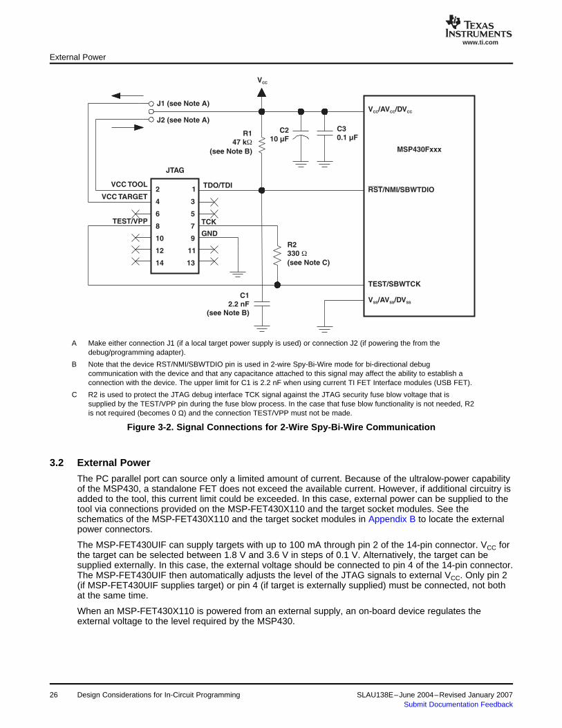
A Make either connection J1 (if a local target power supply is used) or connection J2 (if powering the from thedebug/programming adapter).
B The RST/NMI pin R1/C1 configuration is device-family dependent. See the respective MSP430 family user's guide forthe recommended configuration.
C The TEST/VPP pin is only available on MSP430 family members with multiplexed JTAG pins. See the device datasheet to determine if this pin is available.
D The connection to the JTAG connector RST pin is optional when using 4-wire JTAG communication modecapable-only devices and is not required for device programming or debugging. However, this connection is requiredwhen using 2-wire Spy-Bi-Wire communication mode capable devices in 4-wire JTAG mode.
E When using 2-wire Spy-Bi-Wire communication capable devices in 4-wire JTAG mode, the upper limit for C1 shouldnot exceed 2.2 nF. This applies to both TI FET interface modules (LPT/USB FET).
Figure 3-1. Signal Connections for 4-Wire JTAG Communication
SLAU138E–June 2004–Revised January 2007 Design Considerations for In-Circuit Programming 25Submit Documentation Feedback
www.ti.com
TCK
GND
TEST/VPP
VCC TOOL
VCC TARGET
J2 (see Note A)
VCC
R1
47 k
(see Note B)
W
C2
10 µF
C3
0.1 µF
V /AV /DVCCCC CC
RST/NMI/SBWTDIO
MSP430Fxxx
C1
2.2 nF
(see Note B)
TEST/SBWTCK
V /AV /DVSS SS SS
J1 (see Note A)
JTAG
TDO/TDI1
3
5
7
9
11
13
2
4
6
8
10
12
14
R2
330
(see Note C)
W
3.2 External Power
External Power
A Make either connection J1 (if a local target power supply is used) or connection J2 (if powering the from thedebug/programming adapter).
B Note that the device RST/NMI/SBWTDIO pin is used in 2-wire Spy-Bi-Wire mode for bi-directional debugcommunication with the device and that any capacitance attached to this signal may affect the ability to establish aconnection with the device. The upper limit for C1 is 2.2 nF when using current TI FET Interface modules (USB FET).
C R2 is used to protect the JTAG debug interface TCK signal against the JTAG security fuse blow voltage that issupplied by the TEST/VPP pin during the fuse blow process. In the case that fuse blow functionality is not needed, R2is not required (becomes 0 Ω) and the connection TEST/VPP must not be made.
Figure 3-2. Signal Connections for 2-Wire Spy-Bi-Wire Communication
The PC parallel port can source only a limited amount of current. Because of the ultralow-power capabilityof the MSP430, a standalone FET does not exceed the available current. However, if additional circuitry isadded to the tool, this current limit could be exceeded. In this case, external power can be supplied to thetool via connections provided on the MSP-FET430X110 and the target socket modules. See theschematics of the MSP-FET430X110 and the target socket modules in Appendix B to locate the externalpower connectors.
The MSP-FET430UIF can supply targets with up to 100 mA through pin 2 of the 14-pin connector. VCC forthe target can be selected between 1.8 V and 3.6 V in steps of 0.1 V. Alternatively, the target can besupplied externally. In this case, the external voltage should be connected to pin 4 of the 14-pin connector.The MSP-FET430UIF then automatically adjusts the level of the JTAG signals to external VCC. Only pin 2(if MSP-FET430UIF supplies target) or pin 4 (if target is externally supplied) must be connected, not bothat the same time.
When an MSP-FET430X110 is powered from an external supply, an on-board device regulates theexternal voltage to the level required by the MSP430.
26 Design Considerations for In-Circuit Programming SLAU138E–June 2004–Revised January 2007Submit Documentation Feedback
www.ti.com
3.3 Bootstrap Loader
Bootstrap Loader
When a target socket module is powered from an external supply, the external supply powers the deviceon the target socket module and any user circuitry connected to the target socket module, and the FETinterface module continues to be powered from the PC via the parallel port. If the externally suppliedvoltage differs from that of the FET interface module, the target socket module must be modified so thatthe externally supplied voltage is routed to the FET interface module (so that it may adjust its outputvoltage levels accordingly). See the target socket module schematics in Appendix B.
The JTAG pins provide access to the Flash memory of the MSP430Fxxx devices. On some devices, thesepins are shared with the device port pins, and this sharing of pins can complicate a design (or it maysimply not be possible to do so). As an alternative to using the JTAG pins, most MSP430Fxxx devicescontain a program (a "Bootstrap Loader") that permits the Flash memory to be erased and programmedsimply, using a reduced set of signals. Application reports SLAA089 and SLAA096 fully describe thisinterface. TI does not produce a BSL tool. However, customers can easily develop their own BSL toolsusing the information in the application reports, or BSL tools can be purchased from third parties. See theMSP430 web site for the application reports and a list of MSP430 third-party tool developers.
Texas Instruments suggests that MSP430Fxxx customers design their circuits with the BSL in mind (i.e.,we suggest providing access to these signals via, for example, a header).
See FAQ Hardware #9 for a second alternative to sharing the JTAG and port pins.
The BSL tool requires the following device signals:
• RST/NMI• TEST(1) or TCK• GND• VCC• P1.1• P2.2 or P1.0(2)
(1) If present on device(2) '1xx and '2xx devices use pins P1.1 and P2.2 for the BSL. '4xx devices use pins P1.0 and P1.1 forthe BSL.
SLAU138E–June 2004–Revised January 2007 Design Considerations for In-Circuit Programming 27Submit Documentation Feedback

www.ti.com
Design Considerations for In-Circuit Programming28 SLAU138E–June 2004–Revised January 2007Submit Documentation Feedback
Appendix ASLAU138E–June 2004–Revised January 2007
Frequently Asked Questions
This appendix presents solutions to frequently asked questions regarding hardware,program development, and debugging tools.
Topic .................................................................................................. Page
A.1 Hardware ................................................................................. 30A.2 Program Development (Assembler, C-Compiler, Linker) ................ 31A.3 Debugging (C-SPY) ................................................................... 33
SLAU138E–June 2004–Revised January 2007 Frequently Asked Questions 29Submit Documentation Feedback
www.ti.com
A.1 Hardware
Hardware
1. The state of the device (CPU registers, RAM memory, etc.) is undefined following a reset.Exceptions to the above statement are that the PC is loaded with the word at 0xFFFE (i.e., the resetvector), the status register is cleared, and the peripheral registers (SFRs) are initialized as documentedin the device-family user's guides. C-SPY resets the device after programming it.
2. When the F2274-Socket module (MSP-TS430DA38) is used in Spy-Bi-Wire mode and a low-frequencycrystal is connected to XIN and XOUT the following should be considered:While the application is executing, the debugger polls the target to detect if a breakpoint was reached.In Spy-Bi-Wire mode the RST pin is used to transmit bi-directional debug-data. As the RST and XINpin are adjacent, the low-frequency oscillator is randomly stopped for one or two cycles by crosstalk ofthe debug signal on the RST pin to XIN.Workarounds are:
• use JTAG-Debug-Mode or• activate debugger option 'Release JTAG On Go'. This disables the debugger from polling the
target while the application is running. A manual halt is required to see if a breakpoint was hit. Or• apply an external frequency to XIN.
3. When the MSP-FET430X110 is used as an interface to an MSP430 on the user's circuit (i.e., there isno MSP430 device in the FET socket), the XOUT and XIN signals from the FET should not beconnected to the corresponding pins of the in-circuit MSP430. Similarly, when using the interfacemodule, do not connect the XOUT and XIN signals from the interface module to the corresponding pinsof the in-circuit MSP430.
4. The 14-conductor cable connecting the FET interface module and the target socket module must notexceed 8 inches (20 centimeters) in length.
5. The signal assignment on the 14-conductor cable is identical for the parallel port interface and theUSB FET.
6. To utilize the on-chip ADC voltage references, C6 (10 µF, 6.3 V, low leakage) must be installed onthe target socket module.
7. Crystals/resonators Q1 and Q2 (if applicable) are not provided on the target socket module. ForMSP430 devices that contain user-selectable loading capacitors, the effective capacitance is theselected capacitance plus 3 pF (pad capacitance) divided by two.
8. Crystals/resonators have no effect on the operation of the tool and C-SPY (as any requiredclocking/timing is derived from the internal DCO/FLL).
9. On 20-pin and 28-pin devices with multiplexed port/JTAG pins (P1.4 to P1.7), it is required that"Release JTAG On Go" be selected to use these pins in their port capacity. See Section C.1.2 foradditional information regarding this mechanism.
10. As an alternative to sharing the JTAG and port pins (on 20 and 28 pin devices), consider usingan MSP430 device that is a "superset" of the smaller device. A very powerful feature of theMSP430 is that the family members are code and architecturally compatible, so code developed onone device (for example, one without shared JTAG and port pins) ports effortlessly to another(assuming an equivalent set of peripherals).
11. Information memory may not be blank (erased to 0xFF) when the device is delivered from TI.Customers should erase the information memory before its first usage. Main memory of packageddevices is blank when the device is delivered from TI.
12. The device current increases by approximately 10 µA when a device in low-power mode isstopped (using ESC), and then the low power mode is restored (using Go). This behavior appearsto happen on all devices except the MSP430F12x.
13. The following ZIF sockets are used in the FET tools and target socket modules:
• 14-pin device (PW package): ENPLAS OTS-14-065-01• 20-pin device (PW package): Yamaichi IC189-0202-64• 28-pin device (DW package): Wells-CTI 652 D028• 38-pin device (DA package): Yamaichi IC189-0382-037• 40-pin device (RHA package): Enplas QFN-40B-0.5-01• 48-pin device (DL package): Yamaichi IC51-0482-1163
30 Frequently Asked Questions SLAU138E–June 2004–Revised January 2007Submit Documentation Feedback

www.ti.com
A.2 Program Development (Assembler, C-Compiler, Linker)
Program Development (Assembler, C-Compiler, Linker)
• 64-pin device (PM package): Yamaichi IC51-0644-807• 80-pin device (PN package): Yamaichi IC201-0804-014• 100-pin device (PZ package): Yamaichi IC201-1004-008
ENPLAS: www.enplas.comWells-CTI: www.wellscti.com/Yamaichi: www.yamaichi.us/
14. Supply current measurement on target socket modules. On each module a jumper connects VCCwith VCC430. If this jumper is removed and an ampere meter is connected to the jumper pins, thesupply current of the module can be measured. As the pullup resistor (47 kΩ) on the reset line isconnected to VCC, the MSP430 device sees a marginal voltage at pin RST/NMI if VCC is present andthe jumper is open. Therefore, VCC should be applied after the ampere meter has been connected.
1. The files supplied in the 430\tutor folder work only with the simulator. Do not use the files withthe FET (see FAQ Program Development #11).
2. A common MSP430 "mistake" is to fail to disable the Watchdog mechanism; the Watchdog isenabled by default, and it resets the device if not disabled or properly handled by the application (seeFAQ Program Development #14).
3. When adding source files to a project, do not add files that are included by source files thathave already been added to the project (for example, an .h file within a .c or .s43 file). These filesare added to the project file hierarchy automatically.
4. In assembler, enclosing a string in double quotes ("string") automatically appends a zero byte tothe string (as an end-of-string marker). Enclosing a string in single-quotes ('string') does not.
5. When using the compiler or the assembler, if the last character of a source line is backslash (\),the subsequent carriage return/line feed is ignored (i.e., it is as if the current line and the next lineare a single line). When used in this way, the backslash character is a "line continuation" character.
6. The linker output format must be "Debug information for C-SPY" (.d43) for use with C-SPY.C-SPY does not start otherwise, and an error message is output. C-SPY cannot input a .TXT file.
7. Position-independent code can be generated using Project → Options → General Options →Target → Position-Independent Code.
8. Within the C libraries, GIE (Global Interrupt Enable) is disabled before (and restored after) thehardware multiplier is used. To disable this behavior, contact TI for the source code for theselibraries.
9. It is possible to mix assembler and C programs within the Workbench. See the AssemblerLanguage Interface chapter of the C/C++ Compiler Reference Guide from IAR.
10. The Workbench can produce an object file in Texas Instruments .TXT format. C-SPY cannot input anobject file in Texas Instruments .TXT format. An error message is output in this case.
11. The example programs given in the KickStart documentation (i.e., Demo, Tutor, etc.) are notcorrect. The programs work only in the simulator. However, the programs do not function correctly onan actual device, because the Watchdog mechanism is active. The programs need to be modified todisable the Watchdog mechanism. Disable the Watchdog mechanism with this C-statement:WDTCTL = WDTPW + WDTHOLD;or with this assembler statement:mov.w # WDTPW+WDTHOLD,&WDTCTL
12. Access to MPY using an 8-bit operation is flagged as an error. Within the .h files, 16-bit registersare defined in such a way that 8-bit operations upon them are flagged as an error. This feature isnormally beneficial and can catch register access violations. However, in the case of MPY, it is alsovalid to access this register using 8-bit operators. If 8-bit operators are used to access MPY, theaccess violation check mechanism can be defeated by using "MPY_" to reference the register.Similarly, 16-bit operations on 8-bit registers are flagged.
13. Constant definitions (#define) used within the .h files are effectively reserved and include, forexample, C, Z, N, and V. Do not create program variables with these names.
SLAU138E–June 2004–Revised January 2007 Frequently Asked Questions 31Submit Documentation Feedback

www.ti.com
Program Development (Assembler, C-Compiler, Linker)
14. The CSTARTUP that is implicitly linked with all C applications does not disable the Watchdogtimer. Use WDT = WDTPW + WDTHOLD; to explicitly disable the Watchdog. This statement is best placedin the __low_level_init() function that gets executed before main().If the Watchdog timer is not disabled, and the Watchdog triggers and resets the device duringCSTARTUP, the source screen goes blank, as C-SPY is not able to locate the source code forCSTARTUP. Be aware that CSTARTUP can take a significant amount of time to execute if a largenumber of initialized global variables are used.
int __low_level_init(void)
/* Insert your low-level initializations here */
WDTCTL = WDTPW + WDTHOLD; // Stop Watchdog timer
/*==================================*//* Choose if segment initialization *//* should be done or not. *//* Return: 0 to omit seg_init *//* 1 to run seg_init *//*==================================*/return (1);
15. Compiler optimization can remove unused variables and/or statements that have no effect andcan effect debugging. Optimization: NONE is supported within Project → Options → C/C++ Compiler→ Code → Optimizations. Alternatively, variables can be declared volatile.
16. The IAR tutorial assumes a Full or Baseline version of the Workbench. Within a KickStart system,it is not possible to configure the C compiler to output assembler mnemonics.
17. Existing projects from an IAR 1.x system can be used within the new IAR 2.x/3.x system; refer tothe IAR document migration guide for EW430 x.x. This document is located in <InstallationRoot>\Embedded Workbench x.x\430\doc\migration.htm
18. Assembler projects must reference the code segment (RSEG CODE) to use the Linker →Processing → Fill Unused Code Memory mechanism. No special steps are required to use Linker →Processing → Fill Unused Code Memory with C projects.
19. Ensure that the proper C runtime library is selected for C-only and mixed C/assembly languageprojects (Project → General Options → Library Configuration → Library). For assembly-only projects,the runtime library must not get linked in, otherwise the build fails and a linker error is output (e.g., thatthe RESET vector is allocated twice).
20. Numerous C and C++ runtime libraries are provided with the Workbench:cl430d: C, 64-bit doublescl430dp: C, 64-bit doubles, position independentcl430f: C, 32-bit doublescl430fp: C, 32-bit doubles, position independentdl430d: C++, 64-bit doublesdl430dp: C++, 64-bit doubles, position independentdl430f: C++, 32-bit doublesdl430fp: C++, 32-bit doubles, position independentSee the IAR MSP430 C/C++ compiler reference guide for more information on which library to use.
Frequently Asked Questions32 SLAU138E–June 2004–Revised January 2007Submit Documentation Feedback
www.ti.com
A.3 Debugging (C-SPY)
Debugging (C-SPY)
1. Debugging with C-SPY does not seem to affect an externally connected MSP430 device. Shouldthis be the case, check whether the main debugger menu bar contains a menu item called Simulator. Ifso, an actual C-SPY MSP430 core simulator session is running, and no actual communication with thetarget device is established. Solution: Ensure that the C-SPY driver is set to FET Debugger(Project → Options → Debugger → Setup → Driver).
2. C-SPY reports that it cannot communicate with the device. Possible solutions to this probleminclude:
• Ensure that the correct debug interface is selected; use Project → Options → FET Debugger →Connection.
• Ensure that the correct parallel port (LPT1, 2, or 3) is being specified in the C-SPY configuration inthe case a parallel port MSP-FET430PIF interface is used; use Project → Options → FETDebugger → Connection → Parallel Port → LPT1 (default) or LPT2 or LPT3. Check the PC BIOSfor the parallel port address (0x378, 0x278, 0x3bc), and the parallel port configuration (ECP,Compatible, Bidirectional, or Normal) (see FAQ Debugging #7). For users of IBM ThinkPad™computers, try port specifications LPT2 and LPT3, even if the operating system reports the parallelport is located at LPT1.
• Ensure that no other software application has reserved/taken control of the parallel port (forexample, printer drivers, ZIP drive drivers, etc.) if a parallel port MSP-FET430PIF interface is used.Such software can prevent the C-SPY/FET driver from accessing the parallel port and, hence,communicating with the device.
• It may be necessary to reboot the computer to complete the installation of the required port drivers.• Ensure that the MSP430 device is securely seated in the socket (so that the "fingers" of the socket
completely engage the pins of the device), and that its pin 1 (indicated with a circular indentationon the top surface) aligns with the "1" mark on the PCB.
CAUTION
Possible Damage To Device
Always handle MSP430 devices using a vacuum pick-up tool only; do notuse your fingers, as they can easily bend the device pins and render thedevice useless. Also, always observe and follow proper ESD precautions.
3. C-SPY can download data into RAM, information, and Flash main memories. A warning messageis output if an attempt is made to download data outside of the device memory spaces.
4. C-SPY can debug applications that utilize interrupts and low power modes (see FAQ Debugging#25).
5. C-SPY cannot access the device registers and memory while the device is running. C-SPY willdisplay "-" to indicate that a register/memory field is invalid. The user must stop the device to accessdevice registers and memory. Any displayed register/memory fields are then updated.
6. When C-SPY is started, the Flash memory is erased and the opened file is programmed inaccordance with the download options as set in Project → Options → FET Debugger → DownloadControl. This initial erase and program operations can be disabled selecting Project → Options → FETDebugger → Download Control → Suppress Download. Programming of the Flash can be initiatedmanually with Emulator → Init New Device.
7. The parallel port designators (LPTx) have the following physical addresses: LPT1: 378h, LPT2:278h, LPT3: 3BCh. The configuration of the parallel port (ECP, Compatible, Bidirectional, Normal) isnot significant; ECP seems to work well (see FAQ Debugging #1 for additional hints on solvingcommunication problems between C-SPY and the device.
SLAU138E–June 2004–Revised January 2007 Frequently Asked Questions 33Submit Documentation Feedback
www.ti.com
Debugging (C-SPY)
8. C-SPY may assert RST/NMI to reset the device when C-SPY is started and when the device isprogrammed. The device is also reset by the C-SPY RESET button, and when the device is manuallyreprogrammed (Emulator → Init New Device), and when the JTAG is resynchronized (Emulator →Resynchronize JTAG). When RST/NMI is not asserted (low), C-SPY sets the logic driving RST/NMI tohigh-impedance, and RST/NMI is pulled high via a resistor on the PCB.RST/NMI may get asserted and negated after power is applied when C-SPY is started. RST/NMI maythen get asserted and negated a second time after device initialization is complete.Within C-SPY, Emulator → "Power on" Reset cycles the power to the target to generate a power-onreset.
9. C-SPY can debug a device whose program reconfigures the function of the RST/NMI pin to NMI.10. The level of the XOUT/TCLK pin is undefined when C-SPY resets the device. The logic driving
XOUT/TCLK is set to high-impedance at all other times.11. When making current measurements of the device, ensure that the JTAG control signals are
released (Emulator → Release JTAG on Go), otherwise the device will be powered by the signals onthe JTAG pins and the measurements will be erroneous (see FAQ Debugging #13 and Hardware #11).
12. Most C-SPY settings (breakpoints, etc.) are preserved between sessions.13. When C-SPY has control of the device, the CPU is ON (i.e., it is not in low power mode) regardless
of the settings of the low power mode bits in the status register. Any low power mode conditions will berestored prior to Step or Go. Consequently, do not measure the power consumed by the device whileC-SPY has control of the device. Instead, run your application using Go with JTAG released (see FAQDebugging #11 and Hardware #11).
14. The View → Memory → Memory Fill dialog of C-SPY requires hexadecimal values for StartingAddress, Length, and Value to be preceded with "0x". Otherwise the values are interpreted asdecimal.
15. The Memory debug view of C-SPY (View → Memory) can be used to view the RAM, the informationmemory, and the Flash main memory. The Memory utility of C-SPY can be used to modify the RAM;the information memory and Flash main memory cannot be modified using the Memory utility.The information memory and flash main memory can only be programmed when a project is openedand the data is downloaded to the device, or when Emulator → Init New Device is selected.
16. C-SPY does not permit the individual segments of the information memory and the flash mainmemory to be manipulated separately; consider the information memory to be one contiguousmemory, and the flash main memory to be a second contiguous memory.
17. The Memory window correctly displays the contents of memory where it is present. However, theMemory window incorrectly displays the contents of memory where there is none present.Memory should be used only in the address ranges specified by the device data sheet.
18. C-SPY utilizes the system clock to control the device during debugging. Therefore, device counters,etc., that are clocked by the Main System Clock (MCLK) will be affected when C-SPY hascontrol of the device. Special precautions are taken to minimize the effect upon the Watchdog Timer.The CPU core registers are preserved. All other clock sources (SMCLK, ACLK) and peripheralscontinue to operate normally during emulation. In other words, the Flash Emulation Tool is apartially intrusive tool.Devices that support clock control (Emulator → Advanced → Clock Control) can further minimize theseeffects by selecting to stop the clock(s) during debugging (see FAQ Debugging #23).
19. There is a time after C-SPY performs a reset of the device (when the C-SPY session is firststarted, when the Flash is reprogrammed (via Init New Device), and when JTAG is resynchronized(Resynchronize JTAG)) and before C-SPY has regained control of the device that the device willexecute code normally. This behavior may have side effects. Once C-SPY has regained control ofthe device, it will perform a reset of the device and retain control.
20. When programming the Flash, do not set a breakpoint on the instruction immediately followingthe write to Flash operation. A simple workaround to this limitation is to follow the write to Flashoperation with a NOP, and set a breakpoint on the instruction following the NOP (see FAQ Debugging#22).
21. The Dump Memory length specifier is restricted to four hexadecimal digits (0 to FFFF). Thislimits the number of bytes that can be written from 0 to 65535. Consequently, it is not possible to writememory from 0 to 0xFFFF inclusive, as this would require a length specifier of 65536 (or 10000h).
34 Frequently Asked Questions SLAU138E–June 2004–Revised January 2007Submit Documentation Feedback

www.ti.com
Debugging (C-SPY)
22. Multiple internal machine cycles are required to clear and program the Flash memory. When singlestepping over instructions that manipulate the Flash, control is given back to C-SPY before theseoperations are complete. Consequently, C-SPY updates its memory window with erroneousinformation. A workaround to this behavior is to follow the Flash access instruction with a NOP, andthen step past the NOP before reviewing the effects of the Flash access instruction (see FAQDebugging #20).
23. Peripheral bits that are cleared when read during normal program execution (i.e., interrupt flags)are cleared when read while being debugged (i.e., memory dump, peripheral registers).When using certain MSP430 devices (such as MSP430F15x/16x and MSP430F43x/44x devices), bitsdo not behave this way (i.e., the bits are not cleared by C-SPY read operations).
24. C-SPY cannot be used to debug programs that execute in the RAM of 'F12x and 'F41x devices.A work around to this limitation is to debug programs in Flash.
25. While single stepping with active and enabled interrupts, it can appear that only the interruptservice routine (ISR) is active (i.e., the non-ISR code never appears to execute, and the single stepoperation always stops on the first line of the ISR). However, this behavior is correct because thedevice alwayses process an active and enabled interrupt before processing non-ISR (i.e., mainline)code. A workaround for this behavior is, while within the ISR, to disable the GIE bit on the stack so thatinterrupts are disabled after exiting the ISR. This permits the non-ISR code to be debugged (butwithout interrupts). Interrupts can later be reenabled by setting GIE in the status register in the Registerwindow.On devices with the clock control emulation feature, it may be possible to suspend a clock betweensingle steps and delay an interrupt request (Emulator → Advanced → Clock Control).
26. The base (decimal, hexadecimal, etc.) property of Watch Window variables is not preservedbetween C-SPY sessions; the base reverts to Default Format.
27. On devices equipped with a Data Transfer Controller (DTC), the completion of a data transfer cyclepreempts a single step of a low-power mode instruction. The device advances beyond thelow-power mode instruction only after an interrupt is processed. Until an interrupt is processed, itappear that the single step has no effect. A workaround to this situation is to set a breakpoint on theinstruction following the low-power more instruction, and then execute (Go) to this breakpoint.
28. The transfer of data by the Data Transfer Controller (DTC) may not stop precisely when theDTC is stopped in response to a single step or a breakpoint. When the DTC is enabled and asingle step is performed, one or more bytes of data can be transferred. When the DTC is enabled andconfigured for two-block transfer mode, the DTC may not stop precisely on a block boundary whenstopped in response to a single step or a breakpoint.
29. The C-SPY Register window supports instruction cycle length counters. The cycle counter is onlyactive while single stepping. The count is reset when the device is reset, or the device is run (Go). Thecount can be edited (normally set to zero) at any time.
30. It is possible to use C-SPY to get control of a running device whose state is unknown. Simplyuse C-SPY to program a dummy device, and then start the application with Release JTAG on Goselected. Remove the JTAG connector from the dummy device and connect to the unknown device.Select Debug → Break (or the Stop hand) to stop the unknown device. The state of the device canthen be interrogated.
31. Reseting a program temporarily requires a breakpoint if Project → Options → Debugger → Setup →Run To is enabled. If N or more breakpoints are set, Reset sets a virtual breakpoint and runs to theRun To function. Consequently, it may require a significant amount of time before the programresets (i.e., stops at the Run To function). During this time the C-SPY indicates that the program isrunning, and C-SPY windows may be blank (or may not be correctly updated).
32. Run To Cursor temporarily requires a breakpoint. If N breakpoints are set and virtual breakpoints aredisabled, Run To Cursor incorrectly uses a virtual breakpoint. This results in very slow programexecution.
33. The simulator is a CPU core simulator only; peripherals are not simulated, and interrupts arestatistical events.
34. On devices without data breakpoint capabilities, it's possible to associate with an instruction breakpointan (arbitrarily complex) expression that C-SPY evaluates when the breakpoint is hit. This mechanismcan be used to synthesize a data breakpoint. See the C-SPY documentation for a description of thiscomplex breakpoint mechanism.
SLAU138E–June 2004–Revised January 2007 Frequently Asked Questions 35Submit Documentation Feedback

www.ti.com
Debugging (C-SPY)
35. The ROM Monitor referenced by the C-SPY documentation applies only to older MSP430Exxx(EPROM) based devices; it can be ignored when using the FET and the Flash-based MSP430Fdevices.
36. Special function registers (SFRs) and the peripheral registers are displayed in View → Register.37. The putchar()/getchar() breakpoints are set only if these functions are present (and the
mechanism is enabled). Note that putchar()/getchar() could be indirectly referenced by a libraryfunction.
38. The Flash program/download progress bar does not update gradually. This behavior is to beexpected. The progress bar updates whenever a "chunk" of memory is written to Flash. Thedevelopment tools attempt to minimize the number of program chunks to maximize programmingefficiency. Consequently, it is possible, for example, for a 60K-byte program to be reduced to a singlechunk, and the progress bar is updated until the entire write operation is complete.
36 Frequently Asked Questions SLAU138E–June 2004–Revised January 2007Submit Documentation Feedback
Appendix BSLAU138E–June 2004–Revised January 2007
Hardware
This appendix contains information relating to the FET hardware, including schematicsand PCB pictorials.
Topic .................................................................................................. Page
B.1 Schematics and PCBs ............................................................... 38B.2 MSP-FET430UIF Revision History ............................................... 63
SLAU138E–June 2004–Revised January 2007 Hardware 37Submit Documentation Feedback
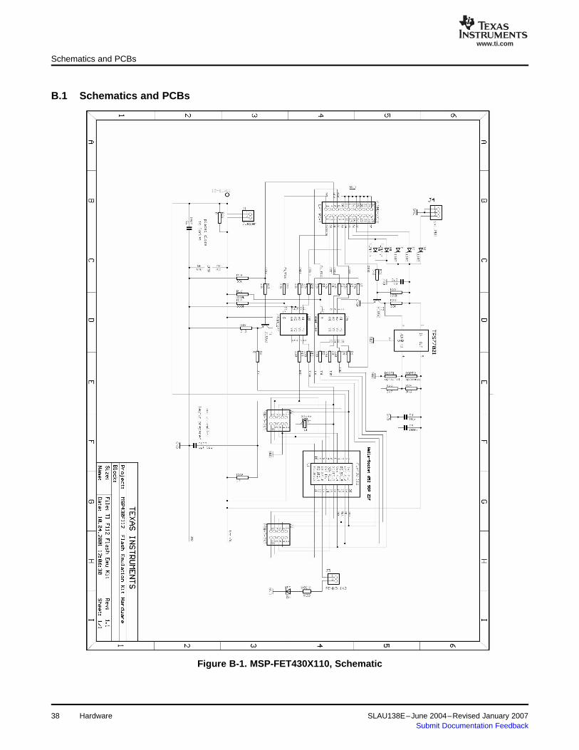
www.ti.com
B.1 Schematics and PCBs
Schematics and PCBs
Figure B-1. MSP-FET430X110, Schematic
38 Hardware SLAU138E–June 2004–Revised January 2007Submit Documentation Feedback
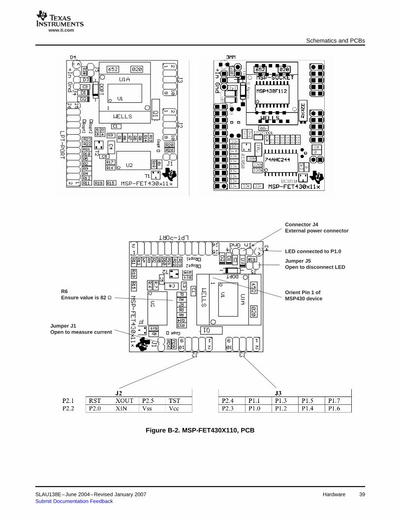
www.ti.com
LED connected to P1.0
Jumper J5Open to disconnect LED
Orient Pin 1 ofMSP430 device
Connector J4External power connector
Jumper J1Open to measure current
R6Ensure value is 82 Ω
Schematics and PCBs
Figure B-2. MSP-FET430X110, PCB
SLAU138E–June 2004–Revised January 2007 Hardware 39Submit Documentation Feedback
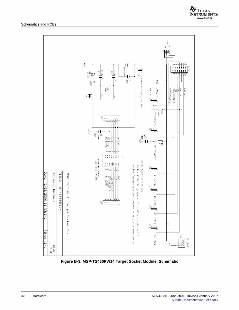
www.ti.com
Schematics and PCBs
Figure B-3. MSP-TS430PW14 Target Socket Module, Schematic
40 Hardware SLAU138E–June 2004–Revised January 2007Submit Documentation Feedback
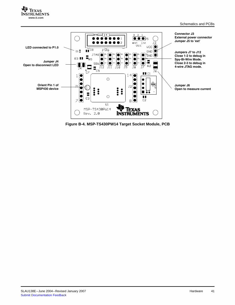
www.ti.com
Jumper J4Open to disconnect LED
Orient Pin 1 ofMSP430 device
Jumper J6Open to measure current
Connector J3External power connectorJumper J5 to 'ext'
LED connected to P1.0
Jumpers J7 to J12Close 1-2 to debug inSpy-Bi-Wire Mode.Close 2-3 to debug in4-wire JTAG mode.
Schematics and PCBs
Figure B-4. MSP-TS430PW14 Target Socket Module, PCB
SLAU138E–June 2004–Revised January 2007 Hardware 41Submit Documentation Feedback
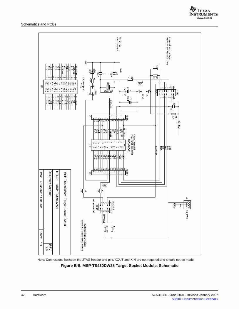
www.ti.com
Schematics and PCBs
Note: Connections between the JTAG header and pins XOUT and XIN are not required and should not be made.
Figure B-5. MSP-TS430DW28 Target Socket Module, Schematic
42 Hardware SLAU138E–June 2004–Revised January 2007Submit Documentation Feedback
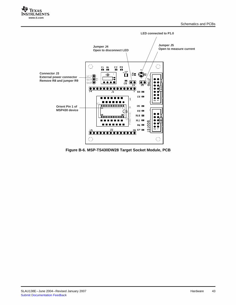
www.ti.com
Jumper J4Open to disconnect LED
Orient Pin 1 ofMSP430 device
Jumper J5Open to measure current
Connector J3External power connectorRemove R8 and jumper R9
LED connected to P1.0
Schematics and PCBs
Figure B-6. MSP-TS430DW28 Target Socket Module, PCB
SLAU138E–June 2004–Revised January 2007 Hardware 43Submit Documentation Feedback
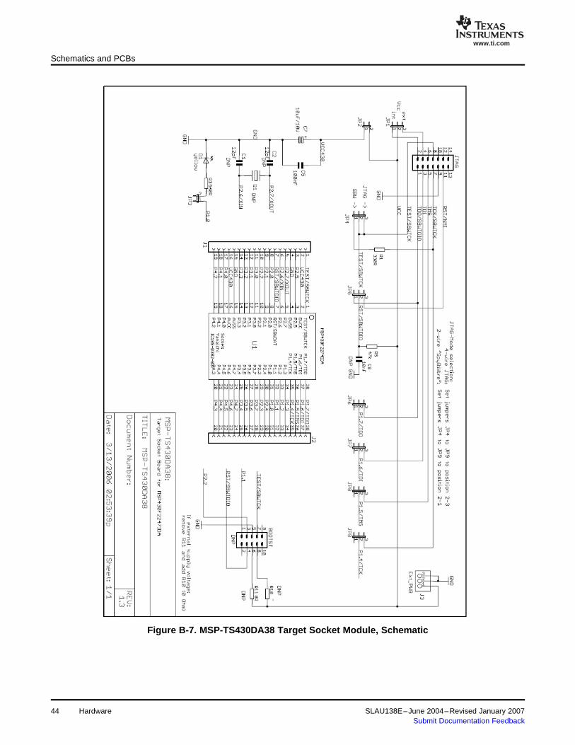
www.ti.com
Schematics and PCBs
Figure B-7. MSP-TS430DA38 Target Socket Module, Schematic
44 Hardware SLAU138E–June 2004–Revised January 2007Submit Documentation Feedback
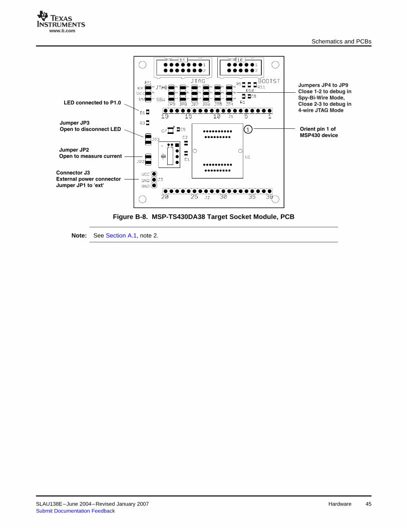
www.ti.com
Orient pin 1 ofMSP430 device
LED connected to P1.0
Connector J3External power connectorJumper JP1 to 'ext'
Jumper JP3Open to disconnect LED
Jumper JP2Open to measure current
Jumpers JP4 to JP9Close 1-2 to debug inSpy-Bi-Wire Mode,Close 2-3 to debug in4-wire JTAG Mode
Schematics and PCBs
Figure B-8. MSP-TS430DA38 Target Socket Module, PCB
Note: See Section A.1, note 2.
SLAU138E–June 2004–Revised January 2007 Hardware 45Submit Documentation Feedback
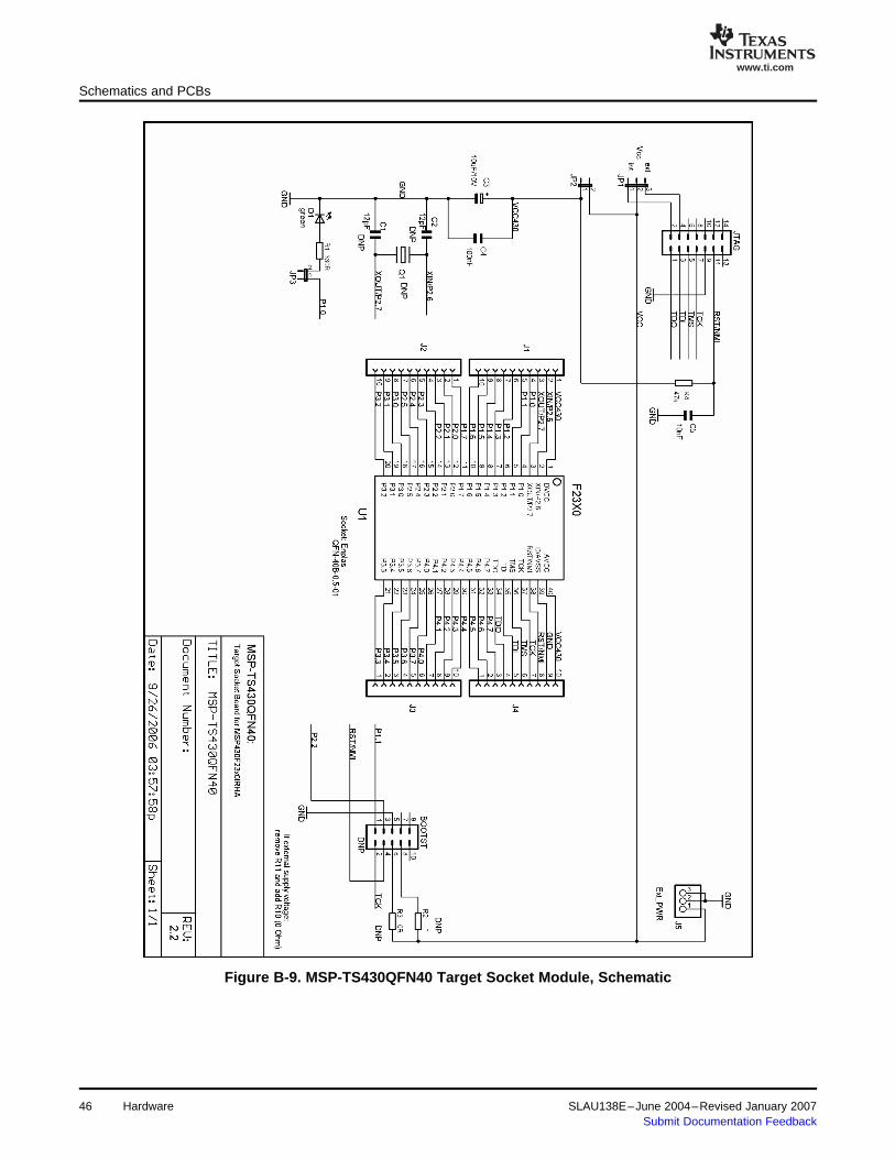
www.ti.com
Schematics and PCBs
Figure B-9. MSP-TS430QFN40 Target Socket Module, Schematic
46 Hardware SLAU138E–June 2004–Revised January 2007Submit Documentation Feedback
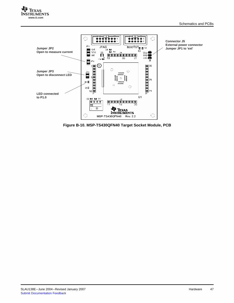
www.ti.com
LED connectedto P1.0
Connector J5External power connectorJumper JP1 to 'ext'
Jumper JP3Open to disconnect LED
Jumper JP2Open to measure current
Schematics and PCBs
Figure B-10. MSP-TS430QFN40 Target Socket Module, PCB
SLAU138E–June 2004–Revised January 2007 Hardware 47Submit Documentation Feedback
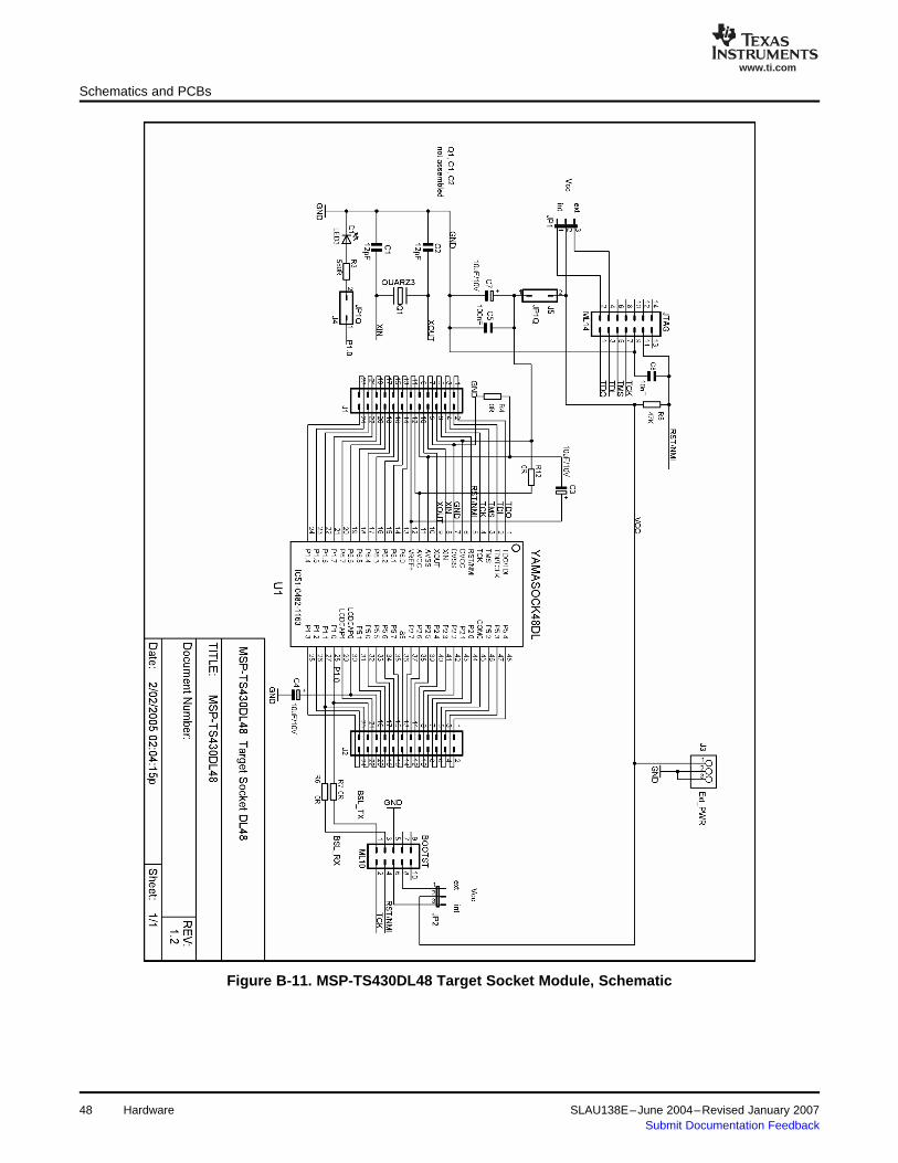
www.ti.com
Schematics and PCBs
Figure B-11. MSP-TS430DL48 Target Socket Module, Schematic
48 Hardware SLAU138E–June 2004–Revised January 2007Submit Documentation Feedback
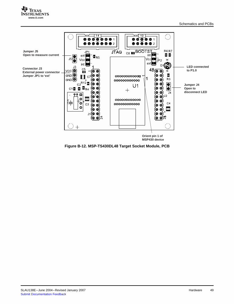
www.ti.com
Jumper J4Open todisconnect LED
LED connectedto P1.0
Orient pin 1 ofMSP430 device
Jumper J5Open to measure current
Connector J3External power connectorJumper JP1 to ‘ext’
Schematics and PCBs
Figure B-12. MSP-TS430DL48 Target Socket Module, PCB
SLAU138E–June 2004–Revised January 2007 Hardware 49Submit Documentation Feedback
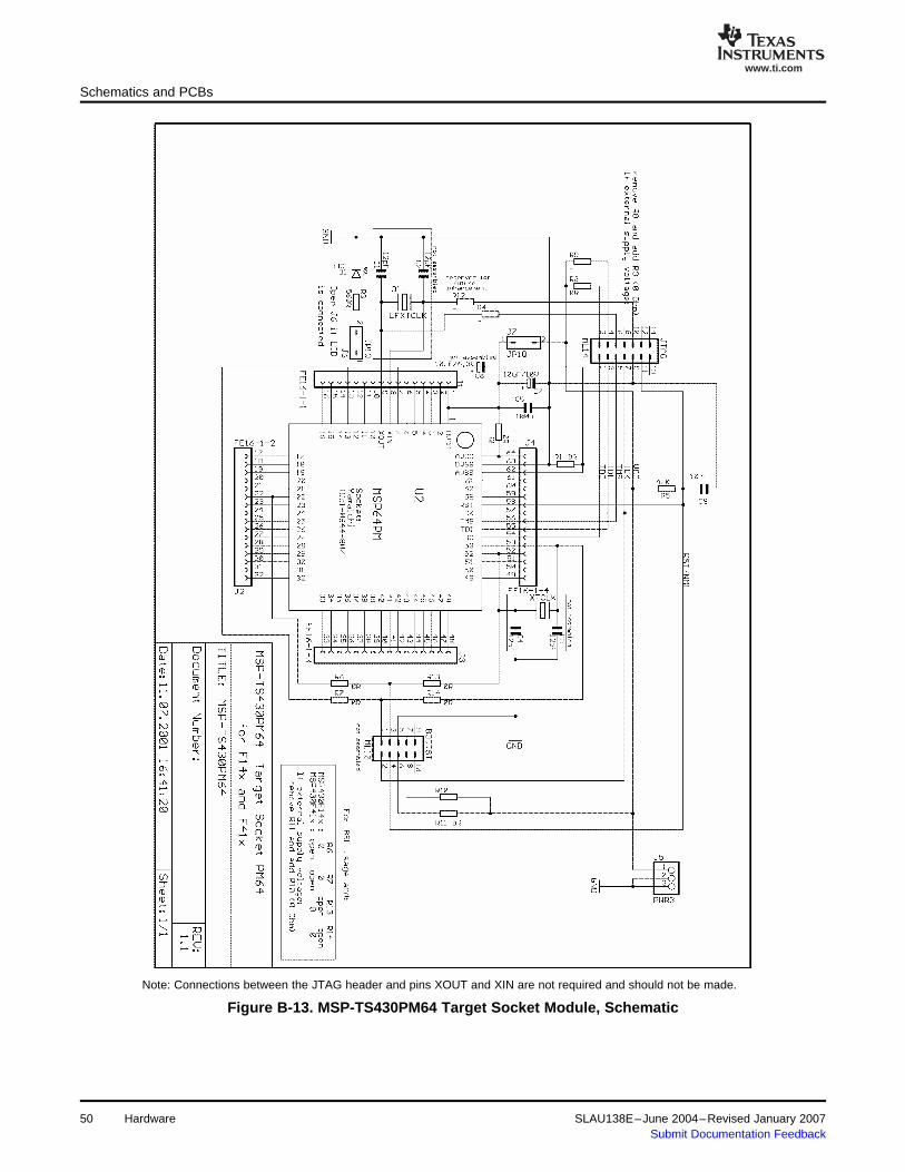
www.ti.com
Schematics and PCBs
Note: Connections between the JTAG header and pins XOUT and XIN are not required and should not be made.
Figure B-13. MSP-TS430PM64 Target Socket Module, Schematic
50 Hardware SLAU138E–June 2004–Revised January 2007Submit Documentation Feedback
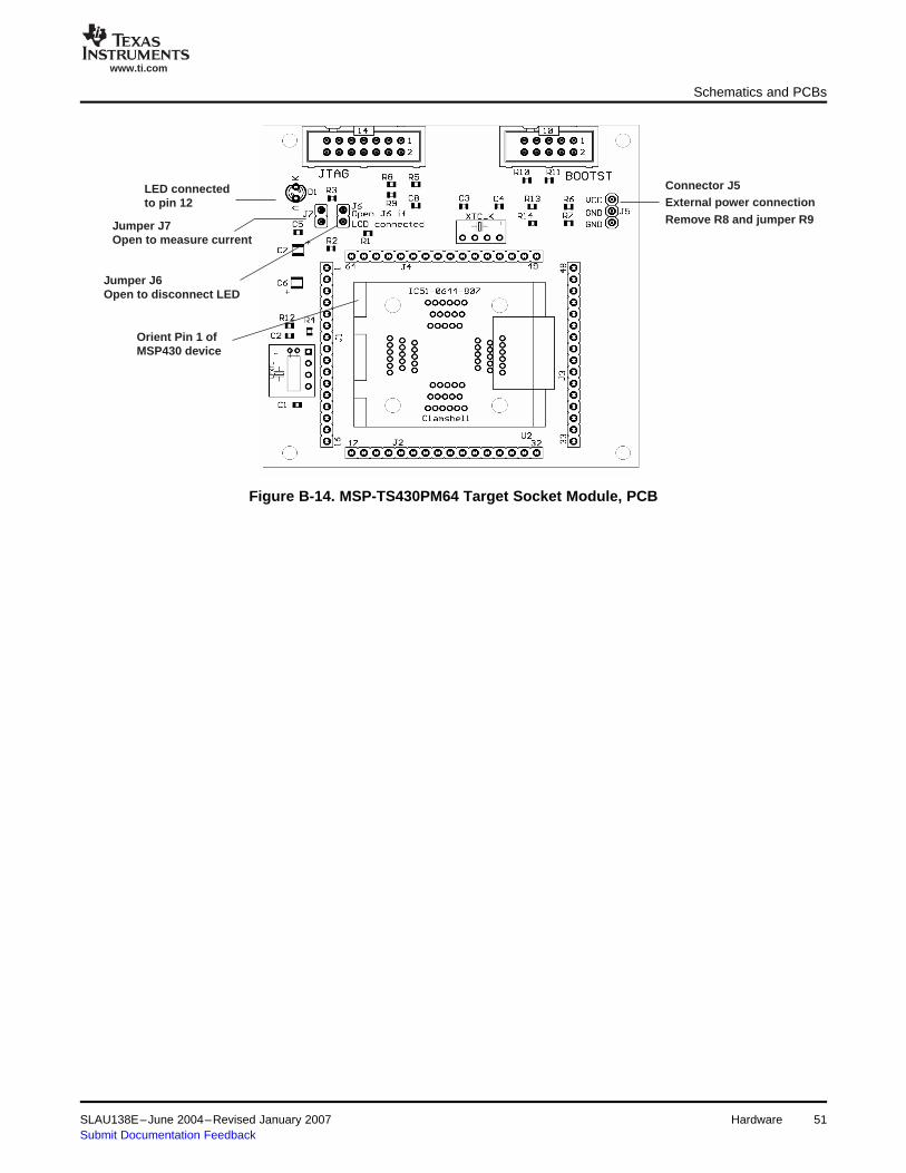
www.ti.com
Connector J5External power connectionRemove R8 and jumper R9
LED connectedto pin 12
Jumper J6Open to disconnect LED
Jumper J7Open to measure current
Orient Pin 1 ofMSP430 device
Schematics and PCBs
Figure B-14. MSP-TS430PM64 Target Socket Module, PCB
SLAU138E–June 2004–Revised January 2007 Hardware 51Submit Documentation Feedback
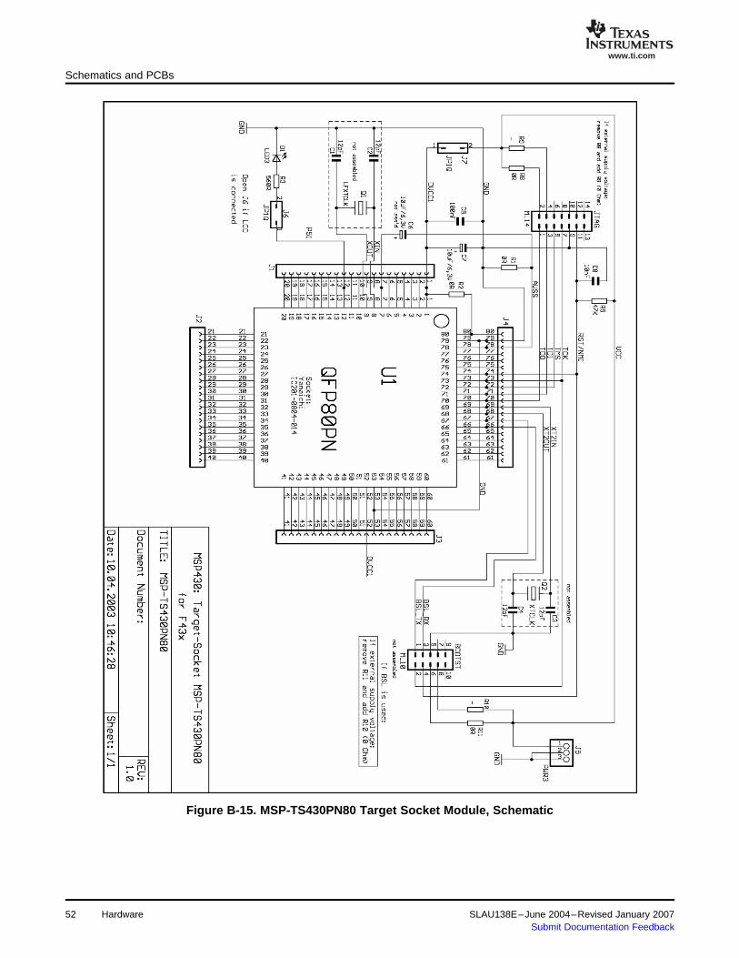
www.ti.com
Schematics and PCBs
Figure B-15. MSP-TS430PN80 Target Socket Module, Schematic
52 Hardware SLAU138E–June 2004–Revised January 2007Submit Documentation Feedback
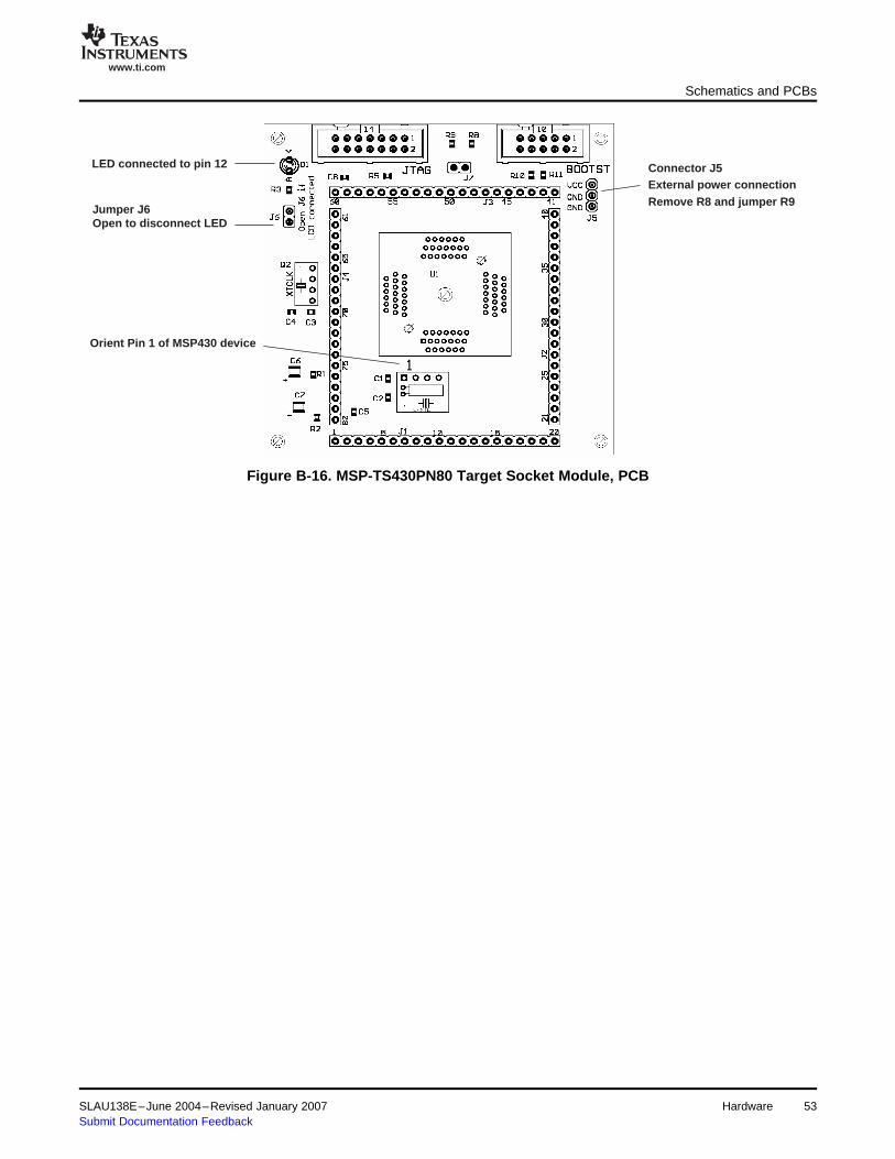
www.ti.com
Connector J5External power connectionRemove R8 and jumper R9
LED connected to pin 12
Jumper J6Open to disconnect LED
Orient Pin 1 of MSP430 device
Schematics and PCBs
Figure B-16. MSP-TS430PN80 Target Socket Module, PCB
SLAU138E–June 2004–Revised January 2007 Hardware 53Submit Documentation Feedback
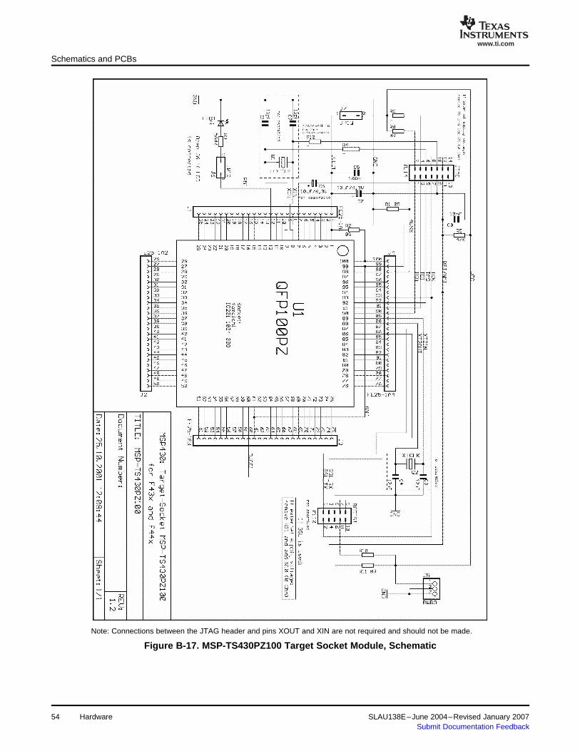
www.ti.com
Schematics and PCBs
Note: Connections between the JTAG header and pins XOUT and XIN are not required and should not be made.
Figure B-17. MSP-TS430PZ100 Target Socket Module, Schematic
54 Hardware SLAU138E–June 2004–Revised January 2007Submit Documentation Feedback
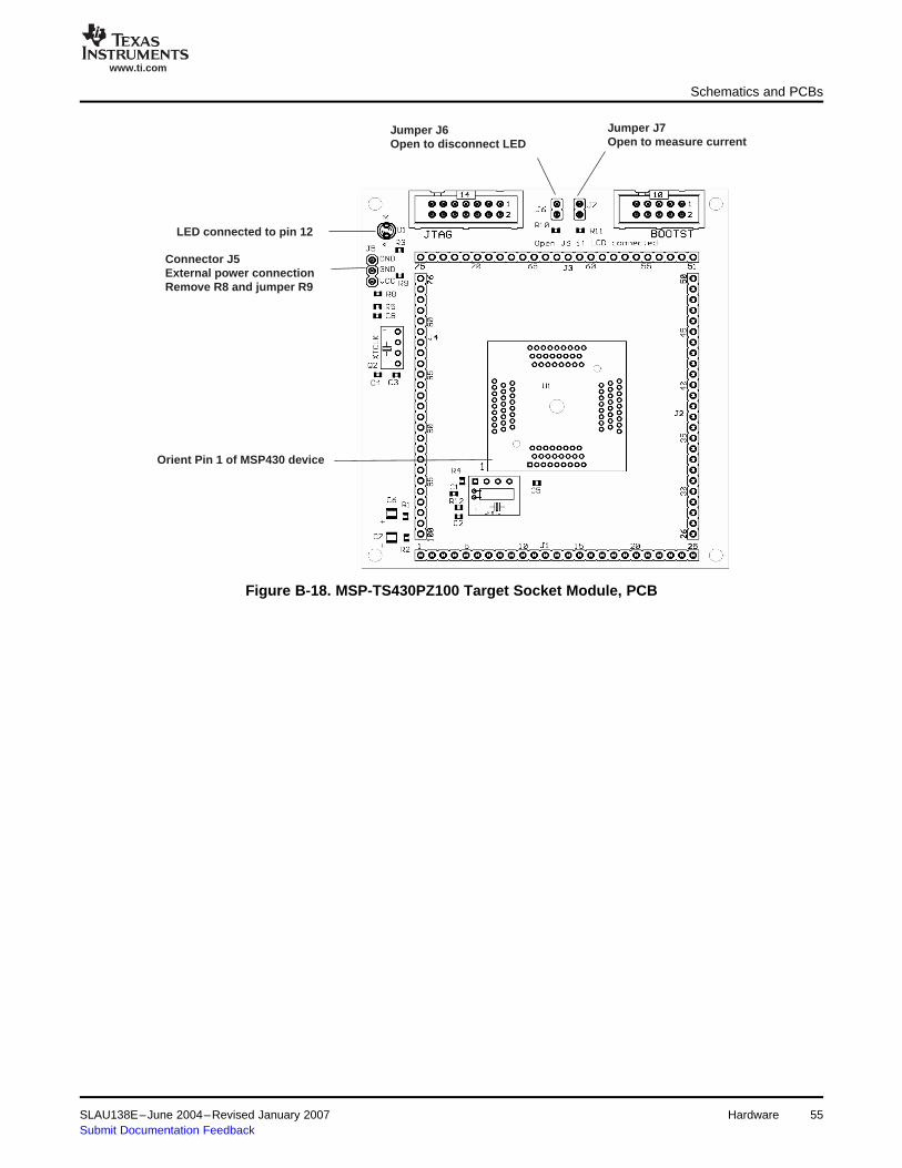
www.ti.com
Connector J5External power connectionRemove R8 and jumper R9
LED connected to pin 12
Jumper J6Open to disconnect LED
Orient Pin 1 of MSP430 device
Jumper J7Open to measure current
Schematics and PCBs
Figure B-18. MSP-TS430PZ100 Target Socket Module, PCB
SLAU138E–June 2004–Revised January 2007 Hardware 55Submit Documentation Feedback
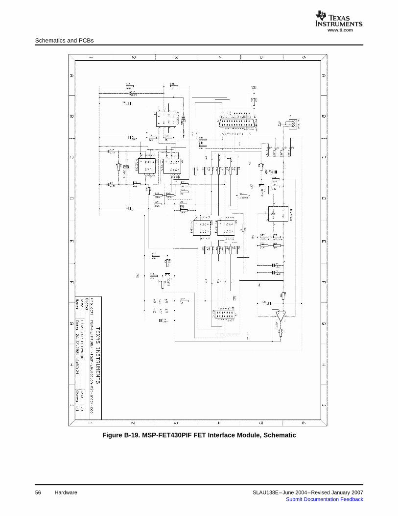
www.ti.com
Schematics and PCBs
Figure B-19. MSP-FET430PIF FET Interface Module, Schematic
56 Hardware SLAU138E–June 2004–Revised January 2007Submit Documentation Feedback
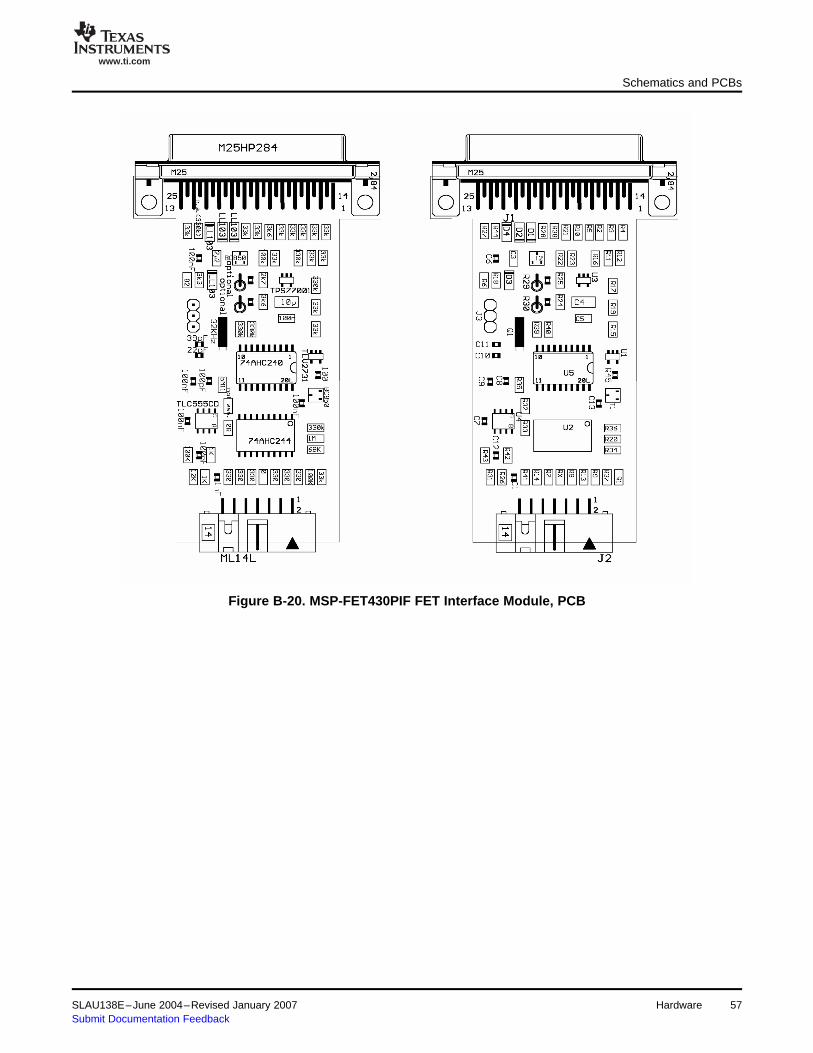
www.ti.com
Schematics and PCBs
Figure B-20. MSP-FET430PIF FET Interface Module, PCB
SLAU138E–June 2004–Revised January 2007 Hardware 57Submit Documentation Feedback
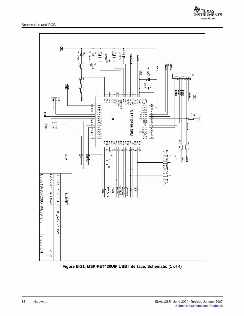
www.ti.com
Schematics and PCBs
Figure B-21. MSP-FET430UIF USB Interface, Schematic (1 of 4)
58 Hardware SLAU138E–June 2004–Revised January 2007Submit Documentation Feedback
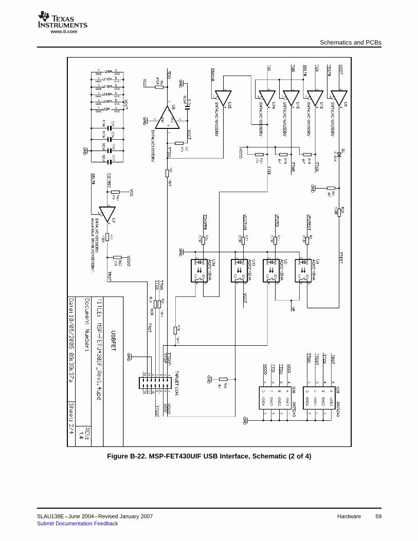
www.ti.com
Schematics and PCBs
Figure B-22. MSP-FET430UIF USB Interface, Schematic (2 of 4)
SLAU138E–June 2004–Revised January 2007 Hardware 59Submit Documentation Feedback
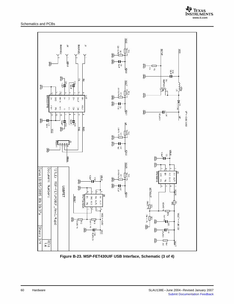
www.ti.com
Schematics and PCBs
Figure B-23. MSP-FET430UIF USB Interface, Schematic (3 of 4)
60 Hardware SLAU138E–June 2004–Revised January 2007Submit Documentation Feedback
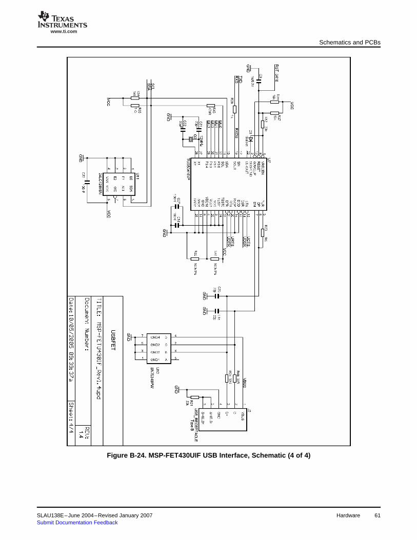
www.ti.com
Schematics and PCBs
Figure B-24. MSP-FET430UIF USB Interface, Schematic (4 of 4)
SLAU138E–June 2004–Revised January 2007 Hardware 61Submit Documentation Feedback
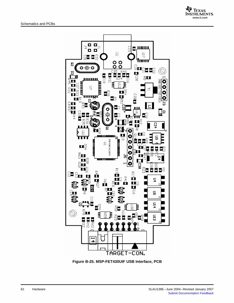
www.ti.com
Schematics and PCBs
Figure B-25. MSP-FET430UIF USB Interface, PCB
Hardware62 SLAU138E–June 2004–Revised January 2007Submit Documentation Feedback
www.ti.com
B.2 MSP-FET430UIF Revision History
MSP-FET430UIF Revision History
Revision 1.3
• Initial released hardware version
Assembly change on 1.3 (May 2005)
• R29, R51, R42, R21, R22, R74: value changed from 330R to 100R
Changes 1.3 to 1.4 (Aug 2005)
• J5: VBUS and RESET additionally connected• R29, R51, R42, R21, R22, R74: value changed from 330R to 100R• U1, U7: F1612 can reset TUSB3410; R44 = 0R added• TARGET-CON: pins 6, 10, 12, 13, 14 disconnected from GND• Firmware-upgrade option through BSL: R49, R52, R53, R54 added; R49, R52 are currently DNP• Pullups on TCK and TMS: R78, R79 added• U2: Changed from SN75LVC1G125DBV to SN75LVC1G07DBV
Assembly change on 1.4 (January 2006)
• R62: not populated
Note: Using a locally powered target board with hardware revision 1.4
Using an MSP-FET430UIF interface hardware revision 1.4 with populated R62 inconjunction with a locally powered target board is not possible. In this case, the targetdevice RESET signal is pulled down by the FET tool. It is recommended to remove R62to eliminate this restriction. This component is located close to the 14-pin connector onthe MSP-FET430UIF PCB. See Figure B-25 for the exact location.
SLAU138E–June 2004–Revised January 2007 Hardware 63Submit Documentation Feedback

www.ti.com
Hardware64 SLAU138E–June 2004–Revised January 2007Submit Documentation Feedback
Appendix CSLAU138E–June 2004–Revised January 2007
FET-Specific Menus
Topic .................................................................................................. Page
C.1 Menus...................................................................................... 66
SLAU138E–June 2004–Revised January 2007 FET-Specific Menus 65Submit Documentation Feedback
www.ti.com
C.1 Menus
C.1.1 Emulator → Device Information
C.1.2 Emulator → Release JTAG on Go
C.1.3 Emulator → Resynchronize JTAG
C.1.4 Emulator → Init New Device
C.1.5 Emulator → Secure - Blow JTAG Fuse
C.1.6 Emulator → Breakpoint usage
C.1.7 Emulator → Advanced → Clock Control
C.1.8 Emulator → Advanced → Emulation Mode
Menus
Opens a window with information about the target device being used. Also, this window allows adjustingthe target voltage in the case an MSP-FET430UIF interface is used to supply power to the target byperforming a right-click inside this window. The supply voltage can be adjusted between 1.8 V and 5 V.This voltage is available on pin 2 of the 14-pin target connector to supply the target from theMSP-FET430UIF. If the target is supplied externally, the external supply voltage should be connected topin 4 of the target connector, so the MSP-FET430UIF can set the level of the output signals accordingly.
C-SPY uses the device JTAG signals to debug the device. On some MSP430 devices, these JTAGsignals are shared with the device port pins. Normally, C-SPY maintains the pins in JTAG mode so thatthe device can be debugged. During this time the port functionality of the shared pins is not available.
However, when Release JTAG On Go is selected, the JTAG drivers are set to tri-state and the device isreleased from JTAG control (TEST pin is set to GND) when Go is activated. Any active on-chipbreakpoints are retained, and the shared JTAG port pins revert to their port functions.
At this time, C-SPY has no access to the device and cannot determine if an active breakpoint (if any) hasbeen reached. C-SPY must be manually commanded to stop the device, at which time the state of thedevice will be determined (i.e., Was a breakpoint reached?) (see FAQ Debugging #11.
Regain control of the device.
It is not possible to Resynchronize JTAG while the device is operating.
Initialize the device according to the settings in the Download Options. Basically, the current program fileis downloaded to the device memory. The device is then reset. This option can be used to programmultiple devices with the same program from within the same C-SPY session.
It is not possible to select Init New Device while the device is operating.
Blows the fuse on the target device. After the fuse is blown, no communication with the device is possible.
List all used hardware and virtual breakpoints, as well as all currently defined EEM breakpoints.
Disable the specified system clock while C-SPY has control of the device (following a Stop or breakpoint).All system clocks are enabled following a Go or a single step (Step/Step Into) (see FAQ Debugging #18).
Specify the device to be emulated. The device must be reset (or reinitialized through Init New Device)following a change to the emulation mode.
See Appendix D.
FET-Specific Menus66 SLAU138E–June 2004–Revised January 2007Submit Documentation Feedback
www.ti.com
C.1.9 Emulator → Advanced → Memory Dump
C.1.10 Emulator → Advanced → Breakpoint Combiner
C.1.11 Emulator → State Storage Control
C.1.12 Emulator → State Storage Window
C.1.13 Emulator → Sequencer Control
C.1.14 Emulator → "Power on" Reset
C.1.15 Emulator → GIE on/off
C.1.16 Emulator → Leave Target Running
C.1.17 Emulator → Force Single Stepping
Menus
Write the specified device memory contents to a specified file. A conventional dialog is displayed thatpermits the user to specify a file name, a memory starting address, and a length. The addressed memoryis then written in a text format to the named file. Options permit the user to select word or byte text format,and address information and register contents can also be appended to the file.
Open the Breakpoint Combiner dialog box. The Breakpoint Combiner dialog box permits one to specifybreakpoint dependencies. A breakpoint will be triggered when the breakpoints are encountered in thespecified order.
Open the State Storage dialog box. The State Storage dialog box permits one to use the state storagemodule. The State Storage Module is not present on all MSP430 derivatives. Refer to Table 2-1 forimplementation details
See the IAR C-SPY FET Debugger section in the MSP430 IAR Embedded Workbench IDE User Guide.
Open the State Storage window, and display the stored state information as configured by the StateStorage dialog.
See the IAR C-SPY FET Debugger section in the MSP430 IAR Embedded Workbench IDE User Guide.
Open the Sequencer dialog box. The Sequencer dialog box permits one to configure the sequencer statemachine.
See the IAR C-SPY FET Debugger section in the MSP430 IAR Embedded Workbench IDE User Guide.
Cycle power to the device to effect a reset.
Enables or disables all interrupts. Needs to be restored manually before Go.
If C-SPY is closed, the target keeps running the user program.
On Go the program is executed by single steps. The cycle counter works correctly only in this mode.
Note: Availability of Emulator → Advanced menus
Not all Emulator → Advanced menus are supported by all MSP430 devices. These menuswill be grayed-out.
SLAU138E–June 2004–Revised January 2007 FET-Specific Menus 67Submit Documentation Feedback

www.ti.com
FET-Specific Menus68 SLAU138E–June 2004–Revised January 2007Submit Documentation Feedback
Appendix DSLAU138E–June 2004–Revised January 2007
80-pin MSP430F44x and MSP430F43x Device Emulation
80-pin MSP430F44x and MSP430F43x devices can be emulated by the 100-pinMSP430F449 device. Table D-1 lists where the pin signals of an 80-pin device appearon the pins of an MSP-TS430PZ100 target socket module.
Note: The MSP-TS430PZ100 must be modified as indicated.SeeSection C.1.8, Emulator → Advanced → Emulation Mode toenable the emulation mode.
Topic .................................................................................................. Page
D.1 F4xx/80-pin Signal Mapping ....................................................... 70
SLAU138E–June 2004–Revised January 2007 80-pin MSP430F44x and MSP430F43x Device Emulation 69Submit Documentation Feedback
www.ti.com
D.1 F4xx/80-pin Signal Mapping
F4xx/80-pin Signal Mapping
Table D-1. F4xx/80-pin Signal Mapping
Connection RequiredMSP430-TS430PZ100F4xx/80-pin Signal F4xx/80-pin Pin Number Between Indicated Pins ofPin Number MSP430-TS430PZ100 Socket
DVcc1 1 1
P6.3/A3 2 2
P6.4/A4 3 3
P6.5/A5 4 4
P6.6/A6 5 5
P6.7/A7 6 6
VREF+ 7 7
XIN 8 8
XOUT 9 9
VeREF+ 10 10
VREF-/VeREF- 11 11
P5.1/S0 12 12
P5.0/S1 13 13
P4.7/S2 14 14 14-46
P4.6/S3 15 15 15-47
P4.5/S4 16 16 16-48
P4.4/S5 17 17 17-49
P4.3/S6 18 16 18-50
P4.2/S7 19 19 19-51
P4.1/S8 20 20 20-62
P4.0/S9 21 21 21-63
S10 22 22
S11 23 23
S12 24 24
S13 25 25
S14 26 26
S15 27 27
S16 28 28
S17 29 29
P2.7/ADC12CLK/S18 30 30
P2.6/CAOUT/S19 31 31
S20 32 32
S21 33 33
S22 34 34
S23 35 35
P3.7/S24 36 36 36-64
P3.6/S25 37 37 37-65
P3.5/S24 38 38 38-66
P3.4/S27 39 39 39-67
P3.3/UCLK0/S28 40 40 40-68
P3.2/SOMI0/S29 41 41 41-69
P3.1/SIMO0/S30 42 42 42-70
70 80-pin MSP430F44x and MSP430F43x Device Emulation SLAU138E–June 2004–Revised January 2007Submit Documentation Feedback

www.ti.com
F4xx/80-pin Signal Mapping
Table D-1. F4xx/80-pin Signal Mapping (continued)
Connection RequiredMSP430-TS430PZ100F4xx/80-pin Signal F4xx/80-pin Pin Number Between Indicated Pins ofPin Number MSP430-TS430PZ100 Socket
P3.0/STE0/S31 43 43 43-71
COM0 44 52 (1)
P5.2/COM1 45 53
P5.3/COM2 46 54
P5.4/COM3 47 55
R03 48 56
P5.5/R13 49 57
P5.6/R23 50 58
P5.7/R33 51 59
DVcc2 52 60
DVss2 53 61
P2.5/URXD0 54 74 (1)
P2.4/UTXD0 55 75
P2.3.TB2 56 76
P2.2/TB1 57 77
P2.1/TB0 58 78
P2.0/TA2 59 79
P1.7/CA1 60 80
P1.6/CA0 61 81
P1.5/TACLK/ACLK 62 82
P1.4/TBCLK/SMCLK 63 83
P1.3/TBOUTH/SVSOUT 64 84
P1.2/TA1 65 85
P1.1/TA0/MCLK 66 86
P1.0/TA0 67 87
XT2OUT 68 88
XT2IN 69 89
TDO/TDI 70 90
TDI 71 91
TMS 72 92
TCK 73 93
RST/NMI 74 94
P6.0/A0 75 95
P6.1/A1 76 96
P6.2/A2 77 97
Avss 78 98
DVss1 79 99
Avcc 80 100
(1) Note discontinuity of pin numbering sequence
SLAU138E–June 2004–Revised January 2007 80-pin MSP430F44x and MSP430F43x Device Emulation 71Submit Documentation Feedback

www.ti.com
80-pin MSP430F44x and MSP430F43x Device Emulation72 SLAU138E–June 2004–Revised January 2007Submit Documentation Feedback
Appendix ESLAU138E–June 2004–Revised January 2007
MSP-FET430UIF Installation Guide
This section describes the hardware installation process of the MSP-FET430UIF USBdebug interface on a PC running Windows XP. The installation procedure for aWindows 2000 system is very similar and therefore not shown here.
Topic .................................................................................................. Page
E.1 Hardware Installation................................................................. 74
SLAU138E–June 2004–Revised January 2007 MSP-FET430UIF Installation Guide 73Submit Documentation Feedback
www.ti.com
E.1 Hardware Installation
Hardware Installation
1. Connect the MSP-FET430UIF USB Debug Interface with a USB cable to a USB port of your PC.2. Windows now should recognize the new hardware as an "MSP430 USB FET x.xx.xx" (see Figure E-1).
Figure E-1. WinXP Hardware Recognition
3. The Hardware Wizard starts automatically and opens the "Found New Hardware Wizard" window.4. Select "Install from a list or specific location (Advanced)" (see Figure E-2).
Figure E-2. WinXP Hardware Wizard
74 MSP-FET430UIF Installation Guide SLAU138E–June 2004–Revised January 2007Submit Documentation Feedback
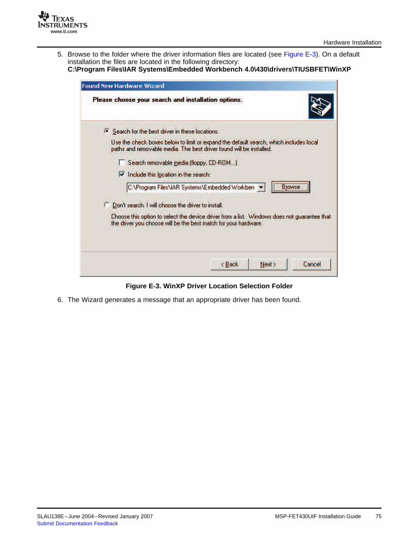
www.ti.com
Hardware Installation
5. Browse to the folder where the driver information files are located (see Figure E-3). On a defaultinstallation the files are located in the following directory:C:\Program Files\IAR Systems\Embedded Workbench 4.0\430\drivers\TIUSBFET\WinXP
Figure E-3. WinXP Driver Location Selection Folder
6. The Wizard generates a message that an appropriate driver has been found.
SLAU138E–June 2004–Revised January 2007 MSP-FET430UIF Installation Guide 75Submit Documentation Feedback
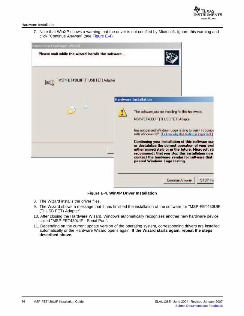
www.ti.com
Hardware Installation
7. Note that WinXP shows a warning that the driver is not certified by Microsoft. Ignore this warning andclick "Continue Anyway" (see Figure E-4).
Figure E-4. WinXP Driver Installation
8. The Wizard installs the driver files.9. The Wizard shows a message that it has finished the installation of the software for "MSP-FET430UIF
(TI USB FET) Adapter".10. After closing the Hardware Wizard, Windows automatically recognizes another new hardware device
called "MSP-FET430UIF - Serial Port".11. Depending on the current update version of the operating system, corresponding drivers are installed
automatically or the Hardware Wizard opens again. If the Wizard starts again, repeat the stepsdescribed above.
76 MSP-FET430UIF Installation Guide SLAU138E–June 2004–Revised January 2007Submit Documentation Feedback
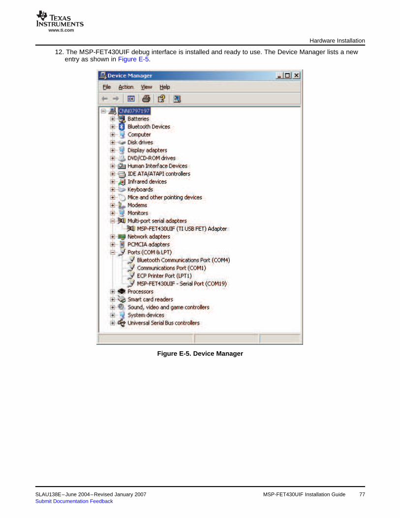
www.ti.com
Hardware Installation
12. The MSP-FET430UIF debug interface is installed and ready to use. The Device Manager lists a newentry as shown in Figure E-5.
Figure E-5. Device Manager
SLAU138E–June 2004–Revised January 2007 MSP-FET430UIF Installation Guide 77Submit Documentation Feedback

EVALUATION BOARD/KIT IMPORTANT NOTICE
Texas Instruments (TI) provides the enclosed product(s) under the following conditions:
This evaluation board/kit is intended for use for ENGINEERING DEVELOPMENT, DEMONSTRATION,OR EVALUATION PURPOSES ONLY and is not considered by TI to be a finished end-product fit forgeneral consumer use. Persons handling the product(s) must have electronics training and observe goodengineering practice standards. As such, the goods being provided are not intended to be complete interms of required design–, marketing–, and/or manufacturing-related protective considerations, includingproduct safety and environmental measures typically found in end products that incorporate suchsemiconductor components or circuit boards. This evaluation board/kit does not fall within the scope of theEuropean Union directives regarding electromagnetic compatibility, restricted substances (RoHS),recycling (WEEE), FCC, CE or UL, and therefore may not meet the technical requirements of thesedirectives or other related directives.
Should this evaluation board/kit not meet the specifications indicated in the User's Guide, the board/kitmay be returned within 30 days from the date of delivery for a full refund. THE FOREGOING WARRANTYIS THE EXCLUSIVE WARRANTY MADE BY SELLER TO BUYER AND IS IN LIEU OF ALL OTHERWARRANTIES, EXPRESSED, IMPLIED, OR STATUTORY, INCLUDING ANY WARRANTY OFMERCHANTABILITY OR FITNESS FOR ANY PARTICULAR PURPOSE.
The user assumes all responsibility and liability for proper and safe handling of the goods. Further, theuser indemnifies TI from all claims arising from the handling or use of the goods. Due to the openconstruction of the product, it is the user's responsibility to take any and all appropriate precautions withregard to electrostatic discharge.
EXCEPT TO THE EXTENT OF THE INDEMNITY SET FORTH ABOVE, NEITHER PARTY SHALL BELIABLE TO THE OTHER FOR ANY INDIRECT, SPECIAL, INCIDENTAL, OR CONSEQUENTIALDAMAGES.
TI currently deals with a variety of customers for products, and therefore our arrangement with the user isnot exclusive.
TI assumes no liability for applications assistance, customer product design, software performance, orinfringement of patents or services described herein.
Please read the User's Guide and, specifically, the Warnings and Restrictions notice in the User's Guideprior to handling the product. This notice contains important safety information about temperatures andvoltages. For additional information on TI's environmental and/or safety programs, please contact the TIapplication engineer or visit www.ti.com/esh.
No license is granted under any patent right or other intellectual property right of TI covering or relating toany machine, process, or combination in which such TI products or services might be or are used.
FCC WARNING
This evaluation board/kit is intended for use for ENGINEERING DEVELOPMENT, DEMONSTRATION,OR EVALUATION PURPOSES ONLY and is not considered by TI to be a finished end-product fit forgeneral consumer use. It generates, uses, and can radiate radio frequency energy and has not beentested for compliance with the limits of computing devices pursuant to part 15 of FCC rules, which aredesigned to provide reasonable protection against radio frequency interference. Operation of thisequipment in other environments may cause interference with radio communications, in which case theuser at his own expense will be required to take whatever measures may be required to correct thisinterference.
Mailing Address
Texas Instruments
Post Office Box 655303
Dallas, Texas 75265

IMPORTANT NOTICE
Texas Instruments Incorporated and its subsidiaries (TI) reserve the right to make corrections, modifications, enhancements, improvements, and other changes to its products and services at any time and to discontinue any product or service without notice. Customers should obtain the latest relevant information before placing orders and should verify that such information is current and complete. All products are sold subject to TI’s terms and conditions of sale supplied at the time of order acknowledgment. TI warrants performance of its hardware products to the specifications applicable at the time of sale in accordance with TI’s standard warranty. Testing and other quality control techniques are used to the extent TI deems necessary to support this warranty. Except where mandated by government requirements, testing of all parameters of each product is not necessarily performed. TI assumes no liability for applications assistance or customer product design. Customers are responsible for their products and applications using TI components. To minimize the risks associated with customer products and applications, customers should provide adequate design and operating safeguards. TI does not warrant or represent that any license, either express or implied, is granted under any TI patent right, copyright, mask work right, or other TI intellectual property right relating to any combination, machine, or process in which TI products or services are used. Information published by TI regarding third-party products or services does not constitute a license from TI to use such products or services or a warranty or endorsement thereof. Use of such information may require a license from a third party under the patents or other intellectual property of the third party, or a license from TI under the patents or other intellectual property of TI. Reproduction of information in TI data books or data sheets is permissible only if reproduction is without alteration and is accompanied by all associated warranties, conditions, limitations, and notices. Reproduction of this information with alteration is an unfair and deceptive business practice. TI is not responsible or liable for such altered documentation. Resale of TI products or services with statements different from or beyond the parameters stated by TI for that product or service voids all express and any implied warranties for the associated TI product or service and is an unfair and deceptive business practice. TI is not responsible or liable for any such statements. Following are URLs where you can obtain information on other Texas Instruments products and application solutions: Products Applications Amplifiers amplifier.ti.com Audio www.ti.com/audio Data Converters dataconverter.ti.com Automotive www.ti.com/automotive DSP dsp.ti.com Broadband www.ti.com/broadband Interface interface.ti.com Digital Control www.ti.com/digitalcontrol Logic logic.ti.com Military www.ti.com/military Power Mgmt power.ti.com Optical Networking www.ti.com/opticalnetwork Microcontrollers microcontroller.ti.com Security www.ti.com/security Low Power Wireless www.ti.com/lpw Telephony www.ti.com/telephony Video & Imaging www.ti.com/video Wireless www.ti.com/wireless Mailing Address: Texas Instruments Post Office Box 655303 Dallas, Texas 75265
Copyright © 2007, Texas Instruments Incorporated