MPLEMENTATION IC M B F IP C - aircconline.comaircconline.com/vlsics/V6N4/6415vlsi05.pdf · I2C...
13
International Journal of VLSI design & Communication Systems (VLSICS) Vol.6, No.4, August 2015 DOI : 10.5121/vlsic.2015.6405 51 ASIC IMPLEMENTATION OF I 2 C MASTER BUS CONTROLLER FIRM IP CORE S Sindhu, Dr. Vijaya Prakash A M and Ankit K V Department of E & C, Bangalore Institute of Technology, Bangalore, KA ABSTRACT ASIC Implementation of I 2 C Master bus controller with design of Firm IP core has been proposed in this paper. I 2 C is one the most prominent protocol used in on chip communication among sub-systems. The generic design of I 2 C master controller has ample of features to incorporate vast varieties of application and I 2 C standards. The generic design is slow, congested and require high power. It’s rare to utilize all the features of generic design fully in a single particular application or system. Hence, a modified ASIC design with specific less features but with better timing, low power requirement and less area overhead, has been proposed in this paper. This design is specifically apt for digital systems which have serial bus interface requirement for on board communication. Moreover, the Firm IP core of I 2 C Master Controller has been designed for ASIC, which makes the design highly portable on any ASIC chips or SOC designs. The firm IPs is best in terms of flexibility and more predictable than commonly found soft IPs. The entire custom ASIC implementation of proposed design has been done in Cadence Tool chain with 45nm technology using standard cell library. A thorough comparison has been done between generic open sourced RTL design of I2C Controller obtained from Opencores.org and our proposed design. KEYWORDS Serial bus interfaces, I 2 C Protocols, ASIC designing, Firm IP Core, on-chip communications, IP designing. 1. INTRODUCTION Communication protocols for data interchange are usually incorporated on digital systems using an on-chip master controller sub-system. The protocols used for communication are generally divided into two broad categories: Parallel and Serial. Parallel buses for all the interfaces are not a good trade-off between cost, time, power and performance. Alternate serial buses are much efficient in on-board data communication between different sub-systems on an IC or SOC. Most of the peripherals on modern ASIC & SOC designs use serial communication buses for data transfers between processor or between processor and peripherals. Few examples of Serial communication protocols are UART, CAN, USB, SPI and Inter IC [2, 4]. The USB, SPI and UARTS can communicate form one device to only one other at a time, i.e. not more than two devices can be connected with each other at a time. Whereas USB has problem of using multiplexer for communication with other devices which makes it bulky [5, 6] . Only I 2 C and CAN protocol uses software addressing but only I 2 C is convenient to design for ICs because CAN is specifically designed for automobiles. The objective of this paper is to develop a Firm IP [9] core of I 2 C Master Bus Controller for ASIC and other applications like SOCs, wherever there is a requirement of compact & small customized I 2 C Protocol Master Bus controller module for communication between on-board components. Now, the VLSI design industry evolving towards smaller sizing. To cope up with this trend, all the inter sub modules of a IC whether main Logical blocks or intercommunication protocols
Transcript of MPLEMENTATION IC M B F IP C - aircconline.comaircconline.com/vlsics/V6N4/6415vlsi05.pdf · I2C...

International Journal of VLSI design & Communication Systems (VLSICS) Vol.6, No.4, August 2015
DOI : 10.5121/vlsic.2015.6405 51
ASIC IMPLEMENTATION OF I2C MASTER BUS
CONTROLLER FIRM IP CORE
S Sindhu, Dr. Vijaya Prakash A M and Ankit K V
Department of E & C, Bangalore Institute of Technology, Bangalore, KA
ABSTRACT
ASIC Implementation of I2C Master bus controller with design of Firm IP core has been proposed in this
paper. I2C is one the most prominent protocol used in on chip communication among sub-systems. The
generic design of I2C master controller has ample of features to incorporate vast varieties of application
and I2C standards. The generic design is slow, congested and require high power. It’s rare to utilize all the
features of generic design fully in a single particular application or system. Hence, a modified ASIC design
with specific less features but with better timing, low power requirement and less area overhead, has been
proposed in this paper. This design is specifically apt for digital systems which have serial bus interface
requirement for on board communication. Moreover, the Firm IP core of I2C Master Controller has been
designed for ASIC, which makes the design highly portable on any ASIC chips or SOC designs. The firm
IPs is best in terms of flexibility and more predictable than commonly found soft IPs. The entire custom
ASIC implementation of proposed design has been done in Cadence Tool chain with 45nm technology using
standard cell library. A thorough comparison has been done between generic open sourced RTL design of
I2C Controller obtained from Opencores.org and our proposed design.
KEYWORDS
Serial bus interfaces, I2C Protocols, ASIC designing, Firm IP Core, on-chip communications, IP designing.
1. INTRODUCTION
Communication protocols for data interchange are usually incorporated on digital systems using
an on-chip master controller sub-system. The protocols used for communication are generally
divided into two broad categories: Parallel and Serial. Parallel buses for all the interfaces are not a
good trade-off between cost, time, power and performance. Alternate serial buses are much
efficient in on-board data communication between different sub-systems on an IC or SOC. Most
of the peripherals on modern ASIC & SOC designs use serial communication buses for data
transfers between processor or between processor and peripherals.
Few examples of Serial communication protocols are UART, CAN, USB, SPI and Inter IC [2, 4].
The USB, SPI and UARTS can communicate form one device to only one other at a time, i.e. not
more than two devices can be connected with each other at a time. Whereas USB has problem of
using multiplexer for communication with other devices which makes it bulky [5, 6] . Only I2C
and CAN protocol uses software addressing but only I2C is convenient to design for ICs because
CAN is specifically designed for automobiles.
The objective of this paper is to develop a Firm IP [9] core of I2C Master Bus Controller for ASIC
and other applications like SOCs, wherever there is a requirement of compact & small customized
I2C Protocol Master Bus controller module for communication between on-board components.
Now, the VLSI design industry evolving towards smaller sizing. To cope up with this trend, all
the inter sub modules of a IC whether main Logical blocks or intercommunication protocols

International Journal of VLSI design & Communication Systems (VLSICS) Vol.6, No.4, August 2015
52
modules like I2C, all have to evolved into new size scaled down versions from bulky past versions
[2,7].
Hence an ASIC implementation of I2C bus module will bring low running cost, high performance,
power efficiency and conciseness to the already available versions, which are generally made for
FPGAs. Moreover Firm IP Core is a recent revolution in IP development industry. So in this
paper a firm IP core design of I2C master controller bus has been proposed which has synthesized
netlist & area, power, timing information as per 45nm standard technology library.
This ASIC implementation of master as firm IP core will have few features but very small size,
min. delay and low power requirements due to modifications in design for specific applications
and also due to technology mapping of 45nm technology library, which is the recent outbreak in
VLSI technology.
2. I2C (INTER-INTEGRATED CIRCUIT) PROTOCOL
I²C protocol with pronunciation as I-squared-C has features like multi slave/master support, serial
communication and single end control. NXP semiconductors now Philips Semiconductor, had
invent I2C protocol [9] for attaching low-speed peripherals with computer main motherboards.
I²C uses only two bidirectional open-drain lines, Serial Data Line (SDA) and Serial Clock Line
(SCL), pulled up with resistors [3]. Typical voltages used are +5 V or +3.3 V although systems
with other voltages are permitted. Standard I2C devices operate up to 100Kbps, while most of the
fast mode I2C devices available today support up to 3.4 Mbps operation [8]. One intermediate
mode is also available which usually works in range of 400Kbps.
2.1. I2C Specification
Standard I²C bus common speeds are up to 10 kbps in low-speed mode and arbitrarily little low
clock frequencies are also allowed sometimes [1]. Recent versions of I²C protocol can host more
number of nodes There is also one other new features of 16-bit addressing. Actual user data
transfer rate is lower than peak bit rates in general. Like if each interaction with a slave
inefficiently allows only 2 byte of data transfer then the data rate will be less than half the peak
bit rate. The design mentioned in figure1 shows bus with a clock (SCL) and data (SDA) lines
have 7bit addressing mode. The bus can take any of two roles for nodes, a master or a slave.
• Master node — this node will generates clock and initialize the communication with
slaves.
• Slave node — these nodes will receives clock and responds when addressed by master.
The bus controller is a multi-master bus hence it can support many number of master nodes.
Moreover, the master and slave roles will be changed between messages (after a STOP sequence
is sent). For a given bus device there may be four potential modes of operation but most devices
use only single role and their two modes where either slave or master sends data, one at a time.

International Journal of VLSI design & Communication Systems (VLSICS) Vol.6, No.4, August 2015
53
Figure 1. I2C bus configuration using Master and Slave
2.2. Working of I2C
Initially the master will come in master transmit mode and start sending a start bit and after that
the 7-bit address of the slave device it wishes to communicate which is followed by a single bit
(the 8th bit) representing whether it wishes to write(0) to or read(1) from the slave device. If any
slave with the sent address exists in the bus line then it will respond with an ACK bit [1] (active
low for acknowledged) for that address sequence. The master then stays in either transmit or
receive mode (as per the read/write bit it sent) while slave continues with the complementary
mode (receive or transmit, respectively). The address and the data bytes are sent as MSB (most
significant bit) first. Start bit is indicated by the high-to-low transition of SDA while the SCL kept
high. And the stop bit is indicated by low-to-high transition on the SDA line keeping SCL high
and rest of the transitions of SDA line take place with SCL low [3,7,8].
3. DESIGN METHODOLOGY
The following section contains all the integral information about the designing of I2C Master
Controller with all components and their description with block diagrams.
3.1. I2C Master Controller
It is the top module which encapsulates a FIFO and a FSM. It allows a proper communication
between the sub modules such as the FIFO and the FSM. The FIFO and the FSM are sequential
and are synchronous in operation with each other, which means both the sub-modules works with
the same clock frequency.
Figure 2. Block Diagram of I2C Master Controller

International Journal of VLSI design & Communication Systems (VLSICS) Vol.6, No.4, August 2015
54
3.2. I2C-FIFO
It is a deep data structure which implements the simple “First In First Out” architecture. The
width of the FIFO is of 15 bits for this proposed design. Whenever the FIFO is full, its filled
status is indicated by the status output signal “full” and whenever there are no values stored in the
FIFO, its empty status is indicated by the status signal “empty”.
3.3. Finite State Machine
FSM is the main component of the I2C master controller in this project. The FSM defined as
sequential circuit which uses the finite number of states to track the history of operations. Eight
states are present in the FSM to get the actual working of the I2C[12].
In general I2C master controller components consists of a Finite State Machine, Clock generator,
Start/Stop controller and counter. In this design, to reduce area penalty, instead of using
individual modules for clock generator, start/stop controller, counter and FSM (Finite State
Machine), the logic for the FSM is written in such a way that it performs the functionality of a
counter, clock generator, and start/stop controller inside only.
Figure 3. Proposed Finite State Machine Diagram
3.4. I2C Clock Generator
It generates the I2C clock signal, which works at a frequency of 100 kbps (standard mode). To
generate 100kbps frequency clock, the board clock signal has to be generated by 512 times in the
clock divided module. The Start, stop and idle states in the FSM only requires the SCL to be high.
Rest of the operations of the SDA line requires negative edge of the SCL clock. This module is
used inside the testbench for functional verification.
3.5 Counter
In the FSM design described above, a local variable is declared which acts like a counter. This
counter will keep track of both the address and data. It Reduce the need of two counter blocks
respectively for address and data, thus reducing area penalty. The 3-bit local variable, which acts
like a counter counts the 7-bit address and the 6-bit data.
3.6 Start/Stop Controller
The Start/Stop Control signals generate and detect start and stop events on the I2C bus. The start
and stop condition detection is necessary to determine whether I2C bus used by another master on
the bus when there are multiple masters on same I2C line. Furthermore, the start detection is

International Journal of VLSI design & Communication Systems (VLSICS) Vol.6, No.4, August 2015
55
necessary for the primary I2C Master Controller because it cannot proceed with a transaction
until the start condition has been accepted by the I2C bus.
3.7 Intellectual Property (IP)
IP’s are the pre-developed integration of pre-developed pieces of functionality in the IC or SOC
design. These IP blocks help the designer to reduce the development cycle time significantly. But,
when an attempt is made to integrate multiple IP’s, the SOC or IC designer has faced tremendous
challenges in understanding these pre-defined functional IP’s and the challenges to made the IP’s
to synchronize with the rest of the IC/SOC. So, in order to avoid the complexity, the IP
component developers and the SOC houses has defined standards for design and integration of
reusable IP’s. The three main standards they have come up with are:
3.7.1 Hard IP
It consists of hard layouts using particular design libraries and is delivered in masked-level
designed blocks. These cores give optimized design and the highest performance for the
particular physical library. The main disadvantage of hard cores is they are technology dependent
and also they provide minimum flexibility and portability [9,11].
3.7.2 Soft IP
Soft IP cores are delivered as RTL VHDL/Verilog code to provide functional descriptions of IP’s
and provides maximum flexibility and re-configurability. But disadvantage is they must be
synthesized, optimized before integration [9, 11].
3.7.3 Firm IP
It has the advantages of both the hard IP and the soft IP. It balances the high performance and
optimization properties of the hard IP’s with the flexibility of soft IP’s. These cores are delivered
in the form of targeted netlist for the specific physical libraries after performing synthesis without
performing the physical layout. The designers can optimize cores for their specific design needs
as the Firm IP blocks are have parameterized circuit descriptions. As the parameters are flexible,
it allows the designers to make the performance more predictable [9, 11].
Figure 4. Comparison of different IP cores
4. IMPLEMENTATION OF DESIGNESIGN METHODOLOGY
The I2C -Master-Controller has been divided into two modules:
• I2C -FIFO
• Finite State Machine
International Journal of VLSI design & Communication Systems (VLSICS) Vol.6, No.4, August 2015
56
I2C FIFO and the Finite State Machine [12] have been designed using Verilog HDL. FSM is a
sequential circuit that uses a finite number [12] of states to keep track of its history of operations,
and the next state is determined based on history of operation and current input. There are several
states in obtaining the functionality of I2C Master Controller operation.
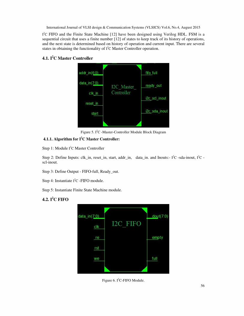
4.1. I2C Master Controller
Figure 5. I2C -Master-Controller Module Block Diagram
4.1.1. Algorithm for I2C Master Controller:
Step 1: Module I2C Master Controller
Step 2: Define Inputs: clk_in, reset_in, start, addr_in, data_in. and Inouts:- I2C -sda-inout, I2C -
scl-inout.
Step 3: Define Output - FIFO-full, Ready_out.
Step 4: Instantiate I2C -FIFO module.
Step 5: Instantiate Finite State Machine module.
4.2. I2C FIFO
Figure 6. I2C-FIFO Module.

International Journal of VLSI design & Communication Systems (VLSICS) Vol.6, No.4, August 2015
57
4.2.1. Algorithm for I2C-FIFO
Step1: Module I2C_FIFO.
Step2: Define Input – clk, rst, din, we, re.
Step3: Define Output – dout, full, empty.
Step4: If clk and rst are equal to 1, then initialize the wptr and rptr to zero.
Step5:If reset is equal to zero and we is high, then increment the write pointer by 1 while If re is
high, then increment the read pointer by 1.
Step6: If wptr is equal to rptr , then empty signal goes high. And reading is not possible from the
FIFO
Step7: If wptr + 1 is equal to rptr, then full signal goes high and Writing is not possible in to the
FIFO.
4.3. Finite State Machine
Algorithm for Finite State Machine:
Step1: An idle State: I2C bus will be in idle state. (SCL and SDA remains logical high).
Step2: Start condition: If the start bit given high, and the sda line is made low when scl line is
high.
Step3: Slave address - write: master sends the slave address to write to the slave.
Step4: If the address matches with the slave address, it sends an acknowledgement by pulling the
sda line low.
Step5: Master sends the 8-bit data on the sda line. After receiving the data, slave acknowledges
by pulling the sda line low.
Step6: Stop condition: After the transmission, master sends the STOP sequence by pulling the sda
line high when the scl clock is high.
Step7: Master transmits slave address and the read signal for read operation to the slave.
Step8: After master receives data from the slave it sends acknowledgement in return to slave.
Step9: Master sends a STOP bit to terminate the connection (SCL is high and SDA is from Low
to high).
International Journal of VLSI design & Communication Systems (VLSICS) Vol.6, No.4, August 2015
58
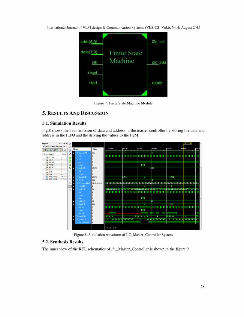
Figure 7. Finite State Machine Module
5. RESULTS AND DISCUSSION
5.1. Simulation Results
Fig.8 shows the Transmission of data and address in the master controller by storing the data and
address in the FIFO and the driving the values to the FSM.
Figure 8. Simulation waveform of I2C_Master_Controller System
5.2. Synthesis Results
The inner view of the RTL schematics of I2C_Master_Controller is shown in the figure 9.
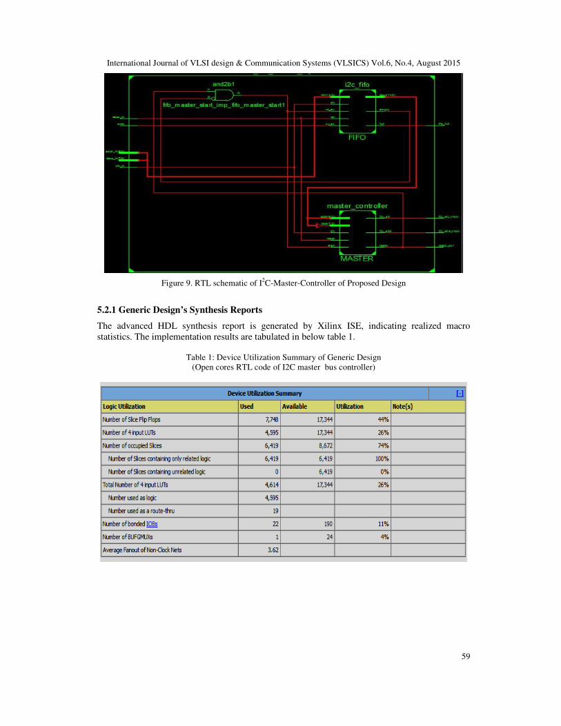
International Journal of VLSI design & Communication Systems (VLSICS) Vol.6, No.4, August 2015
59
Figure 9. RTL schematic of I2C-Master-Controller of Proposed Design
5.2.1 Generic Design’s Synthesis Reports
The advanced HDL synthesis report is generated by Xilinx ISE, indicating realized macro
statistics. The implementation results are tabulated in below table 1.
Table 1: Device Utilization Summary of Generic Design
(Open cores RTL code of I2C master bus controller)
International Journal of VLSI design & Communication Systems (VLSICS) Vol.6, No.4, August 2015
60
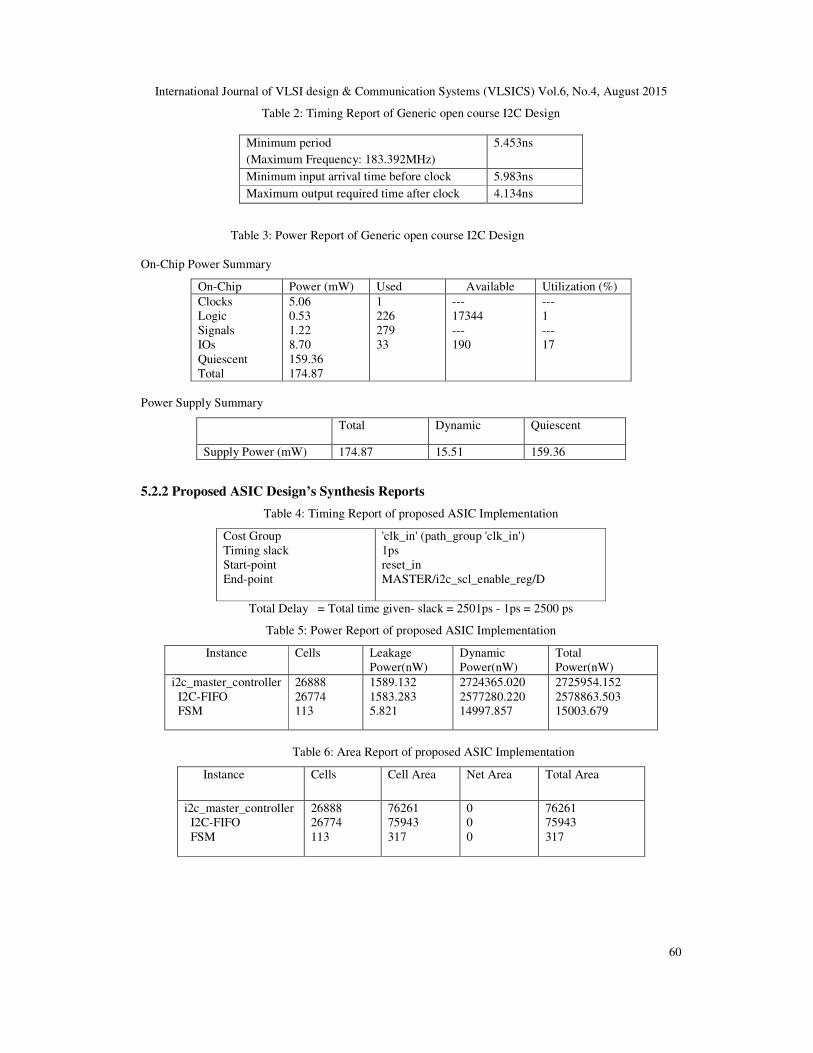
Table 2: Timing Report of Generic open course I2C Design
Minimum period
(Maximum Frequency: 183.392MHz)
5.453ns
Minimum input arrival time before clock 5.983ns
Maximum output required time after clock 4.134ns
Table 3: Power Report of Generic open course I2C Design
On-Chip Power Summary
On-Chip Power (mW) Used Available Utilization (%)
Clocks
Logic
Signals
IOs
Quiescent
Total
5.06
0.53
1.22
8.70
159.36
174.87
1
226
279
33
---
17344
---
190
---
1
---
17
Power Supply Summary
Total
Dynamic Quiescent
Supply Power (mW) 174.87 15.51 159.36
5.2.2 Proposed ASIC Design’s Synthesis Reports
Table 4: Timing Report of proposed ASIC Implementation
Cost Group
Timing slack
Start-point
End-point
'clk_in' (path_group 'clk_in')
1ps
reset_in
MASTER/i2c_scl_enable_reg/D
Total Delay = Total time given- slack = 2501ps - 1ps = 2500 ps
Table 5: Power Report of proposed ASIC Implementation
Instance Cells Leakage
Power(nW)
Dynamic
Power(nW)
Total
Power(nW)
i2c_master_controller
I2C-FIFO
FSM
26888
26774
113
1589.132
1583.283
5.821
2724365.020
2577280.220
14997.857
2725954.152
2578863.503
15003.679
Table 6: Area Report of proposed ASIC Implementation
Instance
Cells Cell Area Net Area Total Area
i2c_master_controller
I2C-FIFO
FSM
26888
26774
113
76261
75943
317
0
0
0
76261
75943
317
International Journal of VLSI design & Communication Systems (VLSICS) Vol.6, No.4, August 2015
61
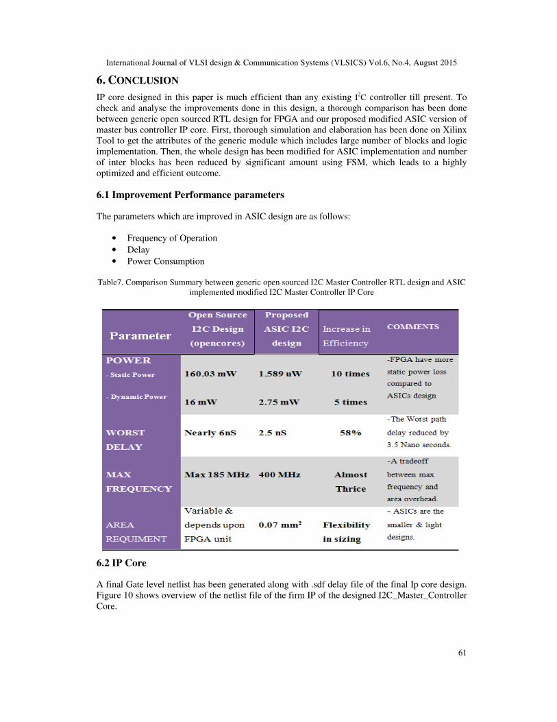
6. CONCLUSION
IP core designed in this paper is much efficient than any existing I2C controller till present. To
check and analyse the improvements done in this design, a thorough comparison has been done
between generic open sourced RTL design for FPGA and our proposed modified ASIC version of
master bus controller IP core. First, thorough simulation and elaboration has been done on Xilinx
Tool to get the attributes of the generic module which includes large number of blocks and logic
implementation. Then, the whole design has been modified for ASIC implementation and number
of inter blocks has been reduced by significant amount using FSM, which leads to a highly
optimized and efficient outcome.
6.1 Improvement Performance parameters
The parameters which are improved in ASIC design are as follows:
• Frequency of Operation
• Delay
• Power Consumption
Table7. Comparison Summary between generic open sourced I2C Master Controller RTL design and ASIC
implemented modified I2C Master Controller IP Core
6.2 IP Core
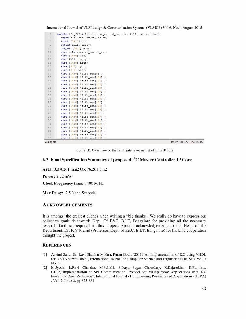
A final Gate level netlist has been generated along with .sdf delay file of the final Ip core design.
Figure 10 shows overview of the netlist file of the firm IP of the designed I2C_Master_Controller
Core.
International Journal of VLSI design & Communication Systems (VLSICS) Vol.6, No.4, August 2015
62
Figure 10. Overview of the final gate level netlist of firm IP core
6.3. Final Specification Summary of proposed I2C Master Controller IP Core
Area: 0.076261 mm2 OR 76,261 um2
Power: 2.72 mW
Clock Frequency (max): 400 M Hz
Max Delay: 2.5 Nano Seconds
ACKNOWLEDGEMENTS
It is amongst the greatest clichés when writing a “big thanks”. We really do have to express our
collective gratitude towards Dept. Of E&C, B.I.T, Bangalore for providing all the necessary
research facilities required in this project. Special acknowledgements to the Head of the
Department, Dr. K V Prasad (Professor, Dept. of E&C, B.I.T, Bangalore) for his kind cooperation
thought the project.
REFERENCES [1] Arvind Sahu, Dr. Ravi Shankar Mishra, Puran Gour, (2011)“An Implementation of I2C using VHDL
for DATA surveillance”, International Journal on Computer Science and Engineering (IJCSE) ,Vol. 3
No. 5
[2] M.Jyothi, L.Ravi Chandra, M.Sahithi, S.Daya Sagar Chowdary, K.Rajasekhar, K.Purnima,
(2012)“Implementation of SPI Communication Protocol for Multipurpose Applications with I2C
Power and Area Reduction”, International Journal of Engineering Research and Applications (IJERA)
, Vol. 2, Issue 2, pp.875-883
International Journal of VLSI design & Communication Systems (VLSICS) Vol.6, No.4, August 2015
63
[3] Bollam Eswari, N.Ponmagal, K.Preethi, S.G.Sreejeesh, (2013) “Implementation of I2C Master Bus
Controller on FPGA”, International conference on Communication and Signal Processing, pp,1113-
1116
[4] A.K. Oudjida, M.L. Berrandjia, R. Tiar, A. Liacha, K. Tahraoui, (2009) “FPGA Implementation of
I2C & SPI Protocols: A Comparative Study” –IEEE Conference on Electronics, Circuits and Systems,
pp. 507 – 510.
[5] Fang Zhao ; Daquan Deng ; Zhensheng Wang ; Huanzhao Liu , ( 2011) “Design of Schematic
Mapping System Based on I2C and USB Bus” –First International Conference on Instrumentation,
Measurement, Computer, Communication and Control, pp. 180-183.
[6] Oberg, J.; Wei Hu ; Irturk, A. ; Tiwari, M.,( 2011) “Information flow isolation in I2C and USB” –
International Conference on Design Automatic Conference(DAC), pp.254-259, 5-9
[7] Narendra Gupta, Vipin Gupta, (2013) “The Performance and Optimization of I2C Protocol using
Verilog on Xilinx Tool” International Journal Of Innovative Research in Electrical, Electronics,
Instrumentation and Control Engineering, vol.1, issue 9.
[8] MR. J. J Patel, PROF B. H. Soni, (2013) ” Design And Implementation Of I2C Bus Controller Using
Verilog” Journal Of Information, Knowledge And Research In Electronics And Communication
Engineering , Volume – 02, Issue - 02
[9] Marcello Dalpasso, Alessandro Bogliolo, and Luca Benini,( 2000) “Hardware/Software IP
protection.” In Proceedings of the 37th Design Automation Conference,pp.593-596, June.
[10] Naagesh S. Bhat, (2011) “Design And ASIC Implementation Of DUC/DDC For Communication
Systems” International Journal of VLSI design & Communication Systems (VLSICS) Vol.2, No.4
[11] Amandeep Singh, Balwinder Singh,(2012) “Microcontroller Based Testing of Digital IP-Core”
International Journal of VLSI design & Communication Systems (VLSICS) Vol.3, No.2
[12] R.Uma And P. Dhavachelvan, (2012) “Synthesis Optimization For Finite State Machine Design In
Fpgas” International Journal of VLSI design & Communication Systems (VLSICS) Vol.3, No.6.
AUTHORS
Vijaya Prakash A.M is working as Professor, Dept. of E&C, BIT, Bangalore. He completed his Ph.D. in
VLSI in the Year 2012. He has many publications in Renowned conferences and International Journals.
His research interests are Low Power VLSI, Synthesis and Optimization. He is a member of IMAPS and
ISTE.
S Sindhu is a PG scholar in Dept. of E&C, BIT, Bangalore, KA, India. She received her B.E degree in
2012 from JNTU, Andhra Pradesh, India. Her research interests are VLSI and communication protocols.
Ankit K V is PG Scholar in Dept. of E&C, BIT, Bangalore, KA, India. He has received B.Tech (Hons) in
ECE and now involved in active research in VLSI Mixed Mode Designs and Embedded Products etc.