MPC5510 Family - Product Brief - NXP...
22
Freescale Semiconductor Product Brief Document Number: MPC5510PB Rev. 2, 5/2008 Contents © Freescale Semiconductor, Inc., 2007, 2008. All rights reserved. The MPC5510 is a new family of next generation microcontrollers built on the Power Architecture. This document describes the features of the family and the options available on the devices in this family. It also provides some important electrical and physical characteristics of these devices. The MPC5510 family of 32-bit microcontrollers is Freescale Semiconductor’s latest achievement in integrated automotive application controllers. It belongs to an expanding family of automotive-focused products designed to address the next wave of central body and gateway applications within the vehicle. Freescale’s advanced and cost efficient host processor core of the MPC5510 automotive controller family is compatible with the Power Architecture Book E architecture. It operates at speeds up to 80 MHz and offers high performance processing optimized for low-power consumption. It capitalizes on the available development infrastructure of the current Power Architecture devices and will be supported with software drivers, operating 1 Application Examples . . . . . . . . . . . . . . . . . . . . . . . . . . . . 2 1.1 Body Controller Application Example . . . . . . . . . . . 2 1.2 Gateway Application Example. . . . . . . . . . . . . . . . . 3 2 Features . . . . . . . . . . . . . . . . . . . . . . . . . . . . . . . . . . . . . . 3 2.1 MPC5510 Family Comparison. . . . . . . . . . . . . . . . . 3 2.2 Block Diagram . . . . . . . . . . . . . . . . . . . . . . . . . . . . . 6 2.3 Critical Performance Parameters . . . . . . . . . . . . . . 7 2.4 Packages. . . . . . . . . . . . . . . . . . . . . . . . . . . . . . . . . 9 2.5 Chip-Level Features . . . . . . . . . . . . . . . . . . . . . . . . 9 2.6 Module Features . . . . . . . . . . . . . . . . . . . . . . . . . . 10 3 Developer Environment . . . . . . . . . . . . . . . . . . . . . . . . . . 21 MPC5510 Family Product Brief 32-Bit Power Architecture™ Microcontrollers for Body Electronics
Transcript of MPC5510 Family - Product Brief - NXP...

Freescale SemiconductorProduct Brief
Document Number: MPC5510PBRev. 2, 5/2008
Contents
The MPC5510 is a new family of next generation microcontrollers built on the Power Architecture.This document describes the features of the family and the options available on the devices in this family. It also provides some important electrical and physical characteristics of these devices.
The MPC5510 family of 32-bit microcontrollers is Freescale Semiconductor’s latest achievement in integrated automotive application controllers. It belongs to an expanding family of automotive-focused products designed to address the next wave of central body and gateway applications within the vehicle. Freescale’s advanced and cost efficient host processor core of the MPC5510 automotive controller family is compatible with the Power Architecture Book E architecture. It operates at speeds up to 80 MHz and offers high performance processing optimized for low-power consumption. It capitalizes on the available development infrastructure of the current Power Architecture devices and will be supported with software drivers, operating
1
2
3
© Freescale Semiconductor, Inc., 2007, 2008. All rights reserved.
Application Examples . . . . . . . . . . . . . . . . . . . . . . . . . . . . 21.1 Body Controller Application Example . . . . . . . . . . . 21.2 Gateway Application Example. . . . . . . . . . . . . . . . . 3Features . . . . . . . . . . . . . . . . . . . . . . . . . . . . . . . . . . . . . . 32.1 MPC5510 Family Comparison. . . . . . . . . . . . . . . . . 32.2 Block Diagram . . . . . . . . . . . . . . . . . . . . . . . . . . . . . 62.3 Critical Performance Parameters . . . . . . . . . . . . . . 72.4 Packages. . . . . . . . . . . . . . . . . . . . . . . . . . . . . . . . . 92.5 Chip-Level Features . . . . . . . . . . . . . . . . . . . . . . . . 92.6 Module Features . . . . . . . . . . . . . . . . . . . . . . . . . . 10Developer Environment. . . . . . . . . . . . . . . . . . . . . . . . . . 21
MPC5510 Family Product Brief32-Bit Power Architecture™ Microcontrollers for Body Electronics

Application Examples
systems, and configuration code to assist with users’ implementations. Refer to Section 3, “Developer Environment,” for more information.
The MPC5510 platform has a single level of memory hierarchy and can support up to 80 KB of on-chip static random access memory (SRAM) and 1.5 MB of internal flash memory. Refer to Table 1 for specific memory and feature sets of the proposed roadmap product members.
1 Application ExamplesThe MPC5510 is designed to address the next wave of central body and gateway applications within the vehicle. As shown in the following examples, the MCU is central to the application and provides the flexibility to add or remove peripheral components in a modular design.
1.1 Body Controller Application ExampleBody controller modules primarily control interior features of the car, such as:
• Comfort features—doors, seats, interior lighting• Security/access features—passive entry, immobilizer, TPMS • Lighting—headlights, brake lights, turn lights • Centralized diagnostic and network management
Figure 1 shows the MPC551xE/S used in a typical body controller application.
Figure 1. Body Controller Application Example
CAN P/I
CAN P/I
MPC551xE/S
Digital outputs
Digital inputs (including
SCI SCI
LIN P/I LIN P/I
Door modules
LS CAN body
HS CAN powertrain
HS CAN diagnostic
Power seat
Steering column
Rain sensor & sunroof controlLIN LIN
input capture signals)
RF receiver
(e.g. PWM,GPIO)
Analog inputs
Smart power(lighting...)
SPI SPI
CAN P/I
Switch panel &digital sensors
Battery monitoring,& misc. sensors
Diagnostic
Direct loads(lighting, power latch,
locking, pumps...)
Mux
MPC5510 Family Product Brief, Rev. 2
Freescale Semiconductor2

Features
1.2 Gateway Application ExampleGateway modules are used in highly distributed architectures to route messages between multiple CAN, LIN, and FlexRay buses. They also manage centralized functions, such as diagnostic, power/wakeup management, and module reprogramming.
Figure 2 shows the MPC551xG used in a typical gateway application.
Figure 2. Gateway Application Example
2 FeaturesThis section describes the features of the MPC5510 family.
2.1 MPC5510 Family ComparisonTable 1 provides a summary of the different members of the MPC5510 family and their proposed features. Great flexibility is offered through multiplexing of I/O functionality. The features available will depend on the specific I/O function assignments in the application. Refer to the pinout information in the reference manual for more details.
Digital outputs (eg PWM,GPIO)
Digital inputsLS CAN body
HS CAN telematics
HS/LS CAN chassis
HS CAN powertrain
HS CAN diagnostic
CAN P/I
CAN P/I
CAN P/I
CAN P/I
Door modules left sideLIN P/I
Direct loads
LIN P/I
MPC551xG
SCI
SCI LIN
LIN
SCI SCI
LIN P/I LIN P/I
Front lighting
Steering column
Switch panels
Wiping
Power seats
Rain sensor & sunroof control
FR P/I
FlexRay backbone
Door modules right side
LIN LIN
Switch panel
CAN P/I
MPC5510 Family Product Brief, Rev. 2
Freescale Semiconductor 3

Table 1. MPC5510 Family Comparison, Maximum Feature Set1
MPC5514G MPC5514EP 144-LQFP 144-LQFP
66 MHz 66 MHz
512 KB 512 KB
64 KB 32 KB
e200z0 e200z0
Yes Yes
16 entry 16 entry
ext 32 KHz Crystal ext 32 KHz Crystal
6x eSCI 6x eSCI
3x DSPI 4x DSPI
cts, but one module can have only five.
18 236
6xFlexCAN
5xFlexCAN
Yes —
Yes Yes
with 16-bit data and four chip selects.
Yes10 Yes10
111 111
NOTES:1 Maximum feature set displayed for each family member. Feature set depends on selected peripheral multiplexing.
Feature MPC5517G MPC5517E MPC5517S MPC5516G MPC5516E MPC5516S MPC5515S
Package 208-BGA 144-LQFP 208-BGA/176-LQFP
144-LQFP 208-BGA/176-LQFP
144-LQFP 208-BGA 144-LQFP 208-BGA/ 176-LQFP
144-LQFP 176-LQFP 144-LQFP 176-LQF
Main CPU e200z1
Maximum Execution Speed2
2 Maximum speed is 66 MHz on 144-LQFP and 176-LQFP package options.
80 MHz at Ta=105C75 MHz at Ta=125C
80 MHz at Ta=105C75 MHz at Ta=125C 66 MHz 80 MHz at Ta=105C
75 MHz at Ta=125C80 MHz at Ta=105C75 MHz at Ta=125C 66 MHz 66 MHz
Flash3
3 EEPROM emulation supported by small flash blocks with read-while-write operation as part of main array space.
1.5 MB 1.5 MB 1.5 MB 1 MB 1 MB 1 MB 768 KB
RAM 80 KB 80 KB 64 KB 64 KB 64 KB 48 KB 48 KB
I/O Processor e200z0 e200z0 — e200z0 e200z0 — —
DMA Yes Yes Yes Yes Yes Yes Yes
MPU 16 entry 16 entry 8 entry 16 entry 16 entry 8 entry 8 entry
ADC4
4 ADC channel accuracy greater for input-only channel, bidirectional channels offer the ability for unused channels to be used as outputs.
40 channels, 12-bit (16 channels input only; 24 channels bidirectional)
Total Timed I/O5
eMIOS200
5 IC—input capture; O/C—output compare; PWM—pulse-width modulation.
24 channels, 16-bit(8 channels IC/OC; 16 channels PWM, IC/OC)
Real-Time Clock ext 32 KHz Crystal ext 32 KHz Crystal — ext 32 KHz Crystal ext 32 KHz Crystal — —
SCI 6x eSCI 6x eSCI 8x eSCI 6x eSCI 6x eSCI 6x eSCI 8x eSCI 6x eSCI 6x eSCI
SPI 4x DSPI 4x DSPI 4x DSPI 4x DSPI 4x DSPI 3x DSPI 3x DSPI
SPI Chip Selects 24 236
6 For devices with four DSPI modules, in the 144-pin package, it is not possible to bring out all 24 DSPI chip selects. Hence, three modules can have six chip sele
24 236 24 236 24 236 24 18 18
CAN 6xFlexCAN
5xFlexCAN
4x FlexCAN
5x FlexCAN
6xFlexCAN
5xFlexCAN
4x FlexCAN
5x FlexCAN
4x FlexCAN
5x FlexCAN
FlexRay Yes — — Yes — — —
MLB7
7 MLB is emulated in software and requires the following resources: I/O Processor, 2xDSPI, 4x eDMA channels, RAM, SoftMLB Interface Logic.
Yes Yes — Yes Yes — —
I2C 1
EBI8
8 In the 208-pin package, there can be up to 24 address bits with 32-bit data and four chip selects. In the 144-pin and 176-pin packages, there are 24 address bits
Yes9
9 16-bit or 32-bit multiplexed data bus supported. EBI multiplexed with other functions shown as available.
Yes10
10 16-bit multiplexed data bus supported. EBI multiplexed with other functions shown as available.
Yes9 Yes10 Yes9 Yes10 Yes9 Yes10 Yes9 — —
GPIO11
11 Estimated I/O count for proposed packages based on multiplexing with peripherals.
144 111 144/137 111 144/137 111 144/137 111 144/137 111 137 111 137

Features
2.1.1 Family Feature Set Scaling
The MPC5510 family supports multiple functions on most of the pins. This allows flexibility in the positioning and the availability of device features. It is the user’s choice what trade-offs are made between the feature set used for the available pin count through this device pin muliplexing. The available features implemented on silicon will be added incrementally as the family functionality increases. Table 2 provides a summary of the flash array address space supported by the different device memory sizes. Table 3 summarizes the RAM array address space supported by the different device memory sizes. Table 4 summarizes the available peripheral functionality of each family member.
Evaluation of the pin list for each device will be necessary, as it may not be possible to retain all modules sequentially, depending on the selected pin multiplexing trade-offs on each device.
NOTEThe RAppID initialization tool provides a pin allocation wizard that will allow you to configure I/O graphically to meet the requirements of the peripheral functions. More information on this tool can be found at http://www.freescale.com/mpc55xx.
Table 2. Flash Memory Scaling Table 3. RAM Memory Scaling
Memory Size Start Address End Address Memory Size Start Address End Address
1.5 MB 0x0000_0000 0x0017_FFFF 80 KB 0x4000_0000 0x4001_3FFF
1 MB 0x0000_0000 0x000F_FFFF 64 KB 0x4000_0000 0x4000_FFFF
768 KB 0x0000_0000 0x000B_FFFF 48 KB 0x4000_0000 0x4000_BFFF
512 KB 0x0000_0000 0x0007_FFFF 32 KB 0x4000_0000 0x4000_7FFF
Table 4. Peripheral Scaling
MPC5517 MPC5516 MPC5515 MPC5514
G E S G E S S G E
Package 208 144 176/208
144 176 144/208 144 176/208
144 176 144 176 144 144
MPU Regions 16 16 16 8 8 16 16 16 8 8 8 8 16 16
SCI Number 6 6 8 6 6 6 6 8 6 6 6 6 6 6
Module A,B,C,D,E,F
A,B,C,D,E,F
A,B,C,D,E,F,G,H
A,B,C,D,E,F
A,B,C,D,E,F
A,B,C,D,E,F
A,B,C,D,E,F
A,B,C,D,E,F,G,H
A,B,C,D,E,F
A,B,C,D,E,F
A,B,C,D,E,F
A,B,C,D,E,F
A,B,C,D,E,F
A,B,C,D,E,F
SPI Number 4 4 4 4 4 4 4 4 3 3 3 3 3 4
Module A,B,C,D A,B,C,D A,B,C,D A,B,C,D A,B,C,D A,B,C,D A,B,C,D A,B,C,D A,B,C A,B,C A,B,C A,B,C A,B,C A,B,C,D
CAN Number 6 5 5 4 5 6 5 5 4 5 4 5 6 5
Module A,B,C,D,E,F
A,C,D,E,F
A,C,D,E,F
A,C,D,E A,C,D,E,F
A,B,C,D,E,F
A,C,D,E,F
A,C,D,E,F
A,C,D,E A,C,D,E,F
A,C,D,E A,C,D,E,F
A,B,C,D,E,F
A,C,D,E,F
MPC5510 Family Product Brief, Rev. 2
Freescale Semiconductor 5

Features
2.2 Block DiagramFigure 3 shows a top level block diagram of the MPC5510 family.
Figure 3. MPC5510 Family Block Diagram
e200z1 Core
LEGEND
eSCI
Data BusInstruction Bus
PrivateInstruction
Bus
Oscillators VREG
ADC
e200z0 Core
eMIOS200
DSPI
I2C
SIU
FlexCAN
BAM
PIT
ADC – Analog to Digital Converter modulesBAM – Boot Assist ModuleDSPI – Serial Peripherals Interface controller moduleEBI – External Bus Interface moduleECC – Error Correction CodeeDMA – enhanced Direct Memory Controller moduleeMIOS200 – Timed Input Output moduleeSCI – Serial Communications Interface modulesFCU – Flash Controller UnitFlexCAN – Controller Area Network controller modules
FlexRay – Dual Channel FlexRay controllerFMPLL – Frequency Modulated Phase Locked Loop moduleI2C – Inter IC Controller modulesINTC – Interrupt Controller moduleJTAG – Joint Test Action Group interfaceMLB – Media Local Bus emulation logicNDI – Nexus Debug Interface modulePIT – Periodic Interrupt Timer moduleSIU – System Integration moduleVREG – Voltage Regulator
MPC5510
IntegerExecution
Unit
InstructionUnit
PPC & VLE
MultiplyUnit
General PurposeRegisters
(32 x 32-bit)
Timers
BranchUnit
Load/StoreUnit
JTAG
NDI
INTC
FlexRay
General PurposeRegisters
(32 x 32-bit)IntegerExecution
Unit
InstructionUnitVLE
BranchUnit
Load/StoreUnit
MultiplyUnit
Crossbar Switch (XBAR)
Memory Protection Unit (MPU)
FCU
Flash(ECC)
SRAM(ECC)
EBIRAM
ControllerPeripheral Bridge
FMPLL
eDMA
MLB
6
MPC5510 Fami
ly Product Brief, Rev. 2Freescale Semiconductor
Features
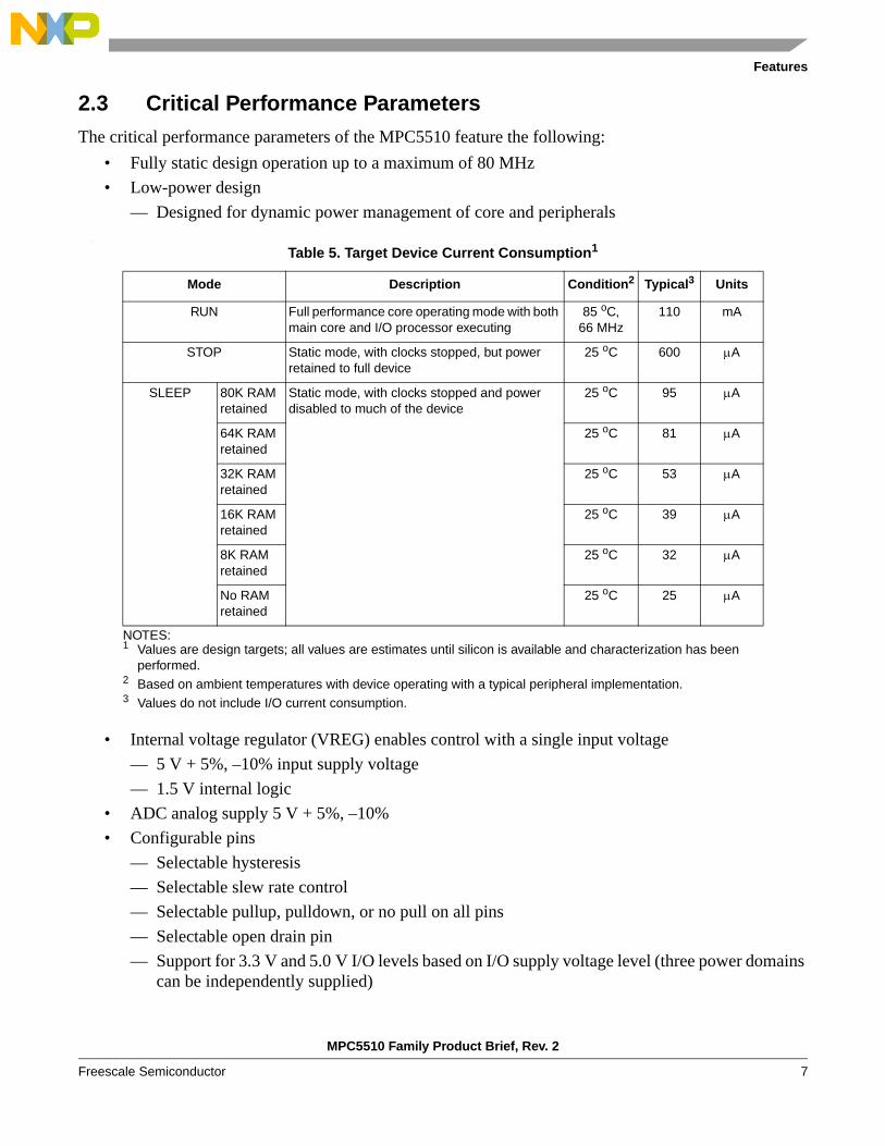
2.3 Critical Performance ParametersThe critical performance parameters of the MPC5510 feature the following:
• Fully static design operation up to a maximum of 80 MHz • Low-power design
— Designed for dynamic power management of core and peripherals:
• Internal voltage regulator (VREG) enables control with a single input voltage — 5 V + 5%, –10% input supply voltage— 1.5 V internal logic
• ADC analog supply 5 V + 5%, –10%• Configurable pins
— Selectable hysteresis — Selectable slew rate control— Selectable pullup, pulldown, or no pull on all pins— Selectable open drain pin— Support for 3.3 V and 5.0 V I/O levels based on I/O supply voltage level (three power domains
can be independently supplied)
Table 5. Target Device Current Consumption1
NOTES:1 Values are design targets; all values are estimates until silicon is available and characterization has been
performed.
Mode Description Condition2
2 Based on ambient temperatures with device operating with a typical peripheral implementation.
Typical3
3 Values do not include I/O current consumption.
Units
RUN Full performance core operating mode with both main core and I/O processor executing
85 oC, 66 MHz
110 mA
STOP Static mode, with clocks stopped, but power retained to full device
25 oC 600 μA
SLEEP 80K RAM retained
Static mode, with clocks stopped and power disabled to much of the device
25 oC 95 μA
64K RAM retained
25 oC 81 μA
32K RAM retained
25 oC 53 μA
16K RAM retained
25 oC 39 μA
8K RAM retained
25 oC 32 μA
No RAM retained
25 oC 25 μA
MPC5510 Family Product Brief, Rev. 2
Freescale Semiconductor 7
Features
• Frequency modulated phase locked loop• –40 to 150 °C junction temperature
2.3.1 Low Power Operation
The MPC5510 has two dynamic power modes and three static power modes:• Low-power modes use clock gating to halt the clock for all or part of the device.• The lowest power modes also use power gating to automatically turn off the power supply to parts
of the device to minimize leakage.• Dynamic power modes are RUN:
— RUN mode is the main full-performance operating mode where the entire device is powered and clocked. The user can configure the device operating speed through selection of the clock source and the phase-locked loop (FMPLL) frequency. Clock gating can be performed on a peripheral by peripheral basis to select which device features have their clock halted to save power. When implemented, the I/O processor can optionally be enabled, allowing execution of code and access to the memory and peripherals of the device.
• Static power modes are STOP and SLEEP:— STOP mode maintains power to the entire device allowing the retention of all on-chip registers
and memory, and providing a fast recovery low-power mode with no need to reconfigure the device. The clocks are halted to the cores and peripherals and the crystal oscillator can be optionally enabled in STOP mode to reduce start-up time, but cannot drive the API/RTC when in this mode.– STOP is entered from RUN mode. On exiting STOP mode the device returns to the RUN
mode.— SLEEP mode halts the clock to the entire device and turns off the power to the majority of the
chip to offer the lowest power consumption modes of the MPC5510. SLEEP mode retains the output levels on the pins, but power gating means that the contents of the cores, on-chip peripheral registers and some of the volatile memory are not held. The device can be awakened from selected I/O pins, a reset, or from a periodic wakeup using a low-power oscillator. If required by the user, it is possible to enable the internal 16 MHz or 32 KHz RC oscillator, or
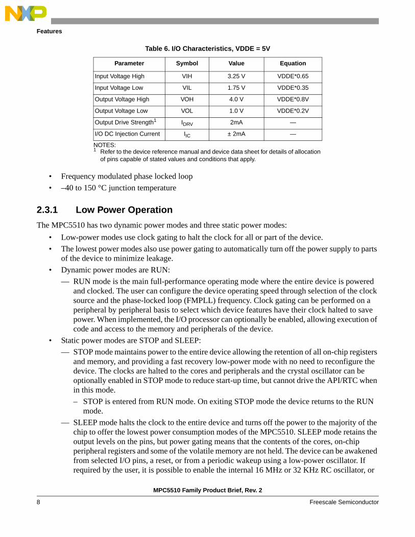
Table 6. I/O Characteristics, VDDE = 5V
Parameter Symbol Value Equation
Input Voltage High VIH 3.25 V VDDE*0.65
Input Voltage Low VIL 1.75 V VDDE*0.35
Output Voltage High VOH 4.0 V VDDE*0.8V
Output Voltage Low VOL 1.0 V VDDE*0.2V
Output Drive Strength1
NOTES:1 Refer to the device reference manual and device data sheet for details of allocation
of pins capable of stated values and conditions that apply.
IDRV 2mA —
I/O DC Injection Current IIC ± 2mA —
MPC5510 Family Product Brief, Rev. 2
Freescale Semiconductor8

Features
an external 32 KHz oscillator. The crystal oscillator can be optionally enabled in SLEEP mode to reduce start-up time. The user can select the desired level of RAM to be retained as the following: full contents of the on-chip PRAM, 80K, 64K, 32K, 16K, 8K, no RAM retained.
— Fast wakeup using the on-chip 16 MHz internal RC oscillator allowing rapid execution on exit from low-power modes.
• 16 MHz internal RC oscillator supports low-speed code execution and clocking of peripherals
2.4 Packages MPC5510 family members are offered in the following package types:
• 144-pin LQFP, 0.5mm pitch, 20mm x 20mm outline• 176-pin LQFP, 0.5 mm pitch, 24mm x 24mm outline• 208-ball MAPBGA, 1mm ball pitch, 17mm × 17mm outline
2.5 Chip-Level FeaturesOn-chip modules available within the family include the following features:
• Single-issue, 32-bit CPU core complex (e200z1)— Compliant with the Power Architecture embedded category— Includes an instruction set enhancement allowing variable length encoding (VLE) for code size
footprint reduction. With the optional encoding of mixed 16-bit and 32-bit instructions, it is possible to achieve significant code-size footprint reduction.
• Up to 1.5 MB of on-chip flash with flash control unit (FCU)• Up to 80 KB on-chip SRAM• Memory protection unit (MPU) with up to 16 region descriptors and 32-byte region granularity• Interrupt controller (INTC) capable of handling selectable-priority interrupt sources• Frequency modulated Phase-locked loop (FMPLL)• Crossbar switch architecture for concurrent access to peripherals, flash, or RAM from multiple bus
masters• One 16-channel enhanced direct memory access controller (eDMA)• Boot assist module (BAM) supports internal flash programming via a serial link (CAN or SCI)• Timer supports input/output channels providing a range of 16-bit input capture, output compare,
and pulse-width modulation functions (eMIOS200)• One 12-bit analog-to-digital converter (ADC)• Up to four serial peripheral interface (DSPI) modules• Up to eight serial communication interface (eSCI) modules• Up to six enhanced full CAN (FlexCAN) modules with configurable buffers • One inter IC communication interface (I2C) module• Up to 144 configurable general-purpose pins supporting input and input/output operations
MPC5510 Family Product Brief, Rev. 2
Freescale Semiconductor 9

Features
• Real-time counter (RTC) with clock source from external 32 KHz crystal oscillator, internal 32 KHz or 16 MHz oscillator and supporting wakeup with selectable 1 sec. resolution and >1 hour timeout, or 1 mS resolution with max timeout of 2 sec.
• Up to eight periodic interrupt timers (PIT) with 32-bit counter resolution• Nexus development interface (NDI) per IEEE-ISTO 5001-2003 Class Two Plus standard• Device/board test support per joint test action group (JTAG) of IEEE (IEEE 1149.1)• On-chip voltage regulator (VREG) regulation of input supply for all internal levels• Optional e200z0, second I/O processor built on Power Architecture technology with VLE
instruction set• Optional FlexRAY controller• Optional external bus interface (EBI) module• Optional medial local bus (MLB) interface for communication with off-chip MOST controller
2.6 Module FeaturesThe following sections provide more detailed information on the modules implemented on the MPC5510.
2.6.1 High Performance e200z1 Core Processor
The e200z1 core includes the following features:• Single-issue four-stage pipelined in-order execution, 32-bit Power Architecture CPU• Supports the 32-bit Power Architecture Book E programmer’s model• Variable length encoding (VLE) enhancements
— Allows optional encoding of mixed 16-bit and 32-bit instructions— Results in smaller code-size footprint— Minimizes impact on performance
• Memory management unit (MMU) with four entry translation look-aside buffer (TLB)— MMU provides features such as VLE or Book-E ISA selection and endianness access control
• Branch processing acceleration using lookahead instruction buffer— Dedicated branch address calculation adder— Branch acceleration using branch lookahead instruction buffer
• Load/store unit— One cycle load latency— Fully pipelined architecture— Misaligned access support— No load-to-use pipeline bubbles
• Thirty-two 32-bit general-purpose registers (GPRs)• Separate instruction bus and load/store bus Harvard architecture
— Private instruction bus to flash controller
MPC5510 Family Product Brief, Rev. 2
Freescale Semiconductor10
Features
• Hardware or software vectored interrupt support• Reservation instructions for implementing read-modify-write constructs• Multi-cycle divide (divw), load multiple (lmw), and store multiple (smw) class instructions; can be
interrupted to prevent increases in interrupt latency• Extensive system development support through Nexus debug port
2.6.2 I/O Processor
The MPC5510’s I/O processor features the following:• The MPC5510 family of devices allows support for flexible implementations, with the option to
select whether the main core is running with or without the I/O processor. This allows tuning of performance against power consumption, and can help smooth out performance peaks while running at a lower speeds. Additionally, the I/O processor can execute when the main core is disabled.
• High-performance, low-cost e200z0 core processor for managing peripherals and interrupts• Single-issue four-stage pipelined in-order execution, 32-bit Power Architecture CPU• Variable length encoding (VLE), allowing mixed 16-bit and 32-bit instructions
— Results in smaller code-size footprint— Minimizes impact on performance
• Branch processing acceleration using lookahead instruction buffer• Load/store unit
— One-cycle load latency— Fully pipelined architecture— Misaligned access support— No load-to-use pipeline bubbles
• Thirty-two 32-bit general purpose registers (GPRs)• Unified interface into crossbar switch• Hardware vectored interrupt support• Reservation instructions for implementing read-modify-write constructs• Multi-cycle divide (divw), load multiple (lmw), and store multiple (smw) class instructions, can be
interrupted to prevent increases in interrupt latency• Extensive system development support through Nexus debug port
2.6.3 Enhanced Direct Memory Access Controller (eDMA)
The following summarizes the MPC5510’s implementation of the eDMA controller:• 16 channels support independent 8, 16, or 32 bit single-value or block transfers• Supports variable sized queues and circular queues• Source and destination address registers are independently configured to post-increment or remain
constant
MPC5510 Family Product Brief, Rev. 2
Freescale Semiconductor 11

Features
• Each transfer is initiated by a peripheral, CPU, periodic timer interrupt, or eDMA channel request• Each eDMA channel can optionally send an interrupt request to the CPU on completion of a single
value or block transfer• DMA transfers possible between system memories, SPIs, SCIs, I2C, ADC, eMIOS200, and general
purpose I/O• Programmable DMA channel mux allows assignment of any DMA source to any available DMA
channel with up to a total of 64 potential request sources
2.6.4 Crossbar Switch (XBAR)
The following summarizes the MPC5510’s implementation of the crossbar switch:• Up to five master ports
— Masters: CPU instruction bus, CPU load/store bus, I/O processor bus, FlexRay, and eDMA• Multiple bus slaves to enable access to flash, SRAM, peripherals, external bus interface (EBI)• Shared port for crossbar access to flash, peripherals bus, and optional external bus interface• Private 32-bit wide instruction bus to flash from main CPU• Crossbar supports up to two consecutive transfers at any one time• 32-bit internal address bus, 32-bit internal data bus• Fixed-priority arbitration based on port master• Temporary dynamic priority elevation of masters
2.6.5 Memory Protection Unit (MPU)
The MPU features the following:• Up to 16 region descriptors for per master protection• Start and end address defined with 32-byte granularity• Overlapping regions supported• Protection attributes can optionally include process ID• Protection offered for three concurrent read ports• Read and write attributes for all masters• Execute and supervisor/user mode attributes for processor masters
2.6.6 Interrupt Controller (INTC)
The MPC5510 implements an interrupt controller that features the following:• Unique 9-bit vector for each of the separate interrupt sources• 8 software-triggerable interrupt sources• 16 priority levels with fixed hardware arbitration within priority levels for each interrupt source• Ability to modify the ISR or task priority.
MPC5510 Family Product Brief, Rev. 2
Freescale Semiconductor12

Features
— Modifying the priority can be used to implement the priority ceiling protocol for accessing shared resources
• Interrupt steering between main CPU and I/O processor— Independent selection of any interrupt source to be routed through I/O processor— Interrupts share same priority level between I/O processor and CPU
• Two external high-priority interrupts directly accessing the main core and IOP critical interrupt mechanism
2.6.7 System Clocks and Clock Generation
The following list summarizes the system clock and clock generation on the MPC5510:• System clock can be derived from the following sources
— External oscillator— FMPLL— 16 MHz internal RC oscillator
• Programmable output clock divider of system clock (÷1, ÷2, ÷4, ÷8)• Separate programmable peripheral bus clock divider ratio (÷1, ÷2, ÷4, ÷8) applied to system clock• Frequency modulated Phase-locked loop (FMPLL)
— Input clock frequency from 4 MHz to 40 MHz— Optional frequency modulation— Lock detect circuitry continuously monitors lock status— Loss-of-clock (LOC) detection for reference and feedback clocks— On-chip loop filter (for improved electomagnetic interference performance and reduces
number of external components required)• On-chip crystal oscillator • Dedicated 16 MHz internal RC oscillator
— Used as default clock source out of reset (can provide a back-up clock in the event of PLL or external oscillator clock failure)
— Provides a clock for rapid start-up from low-power modes— Offers an independent clock source for the watchdog timer— 5% accuracy (after factory trim loaded). Application trim resolution ± 0.5%— Trimming registers to support frequency adjustment with in-application calibration
• Dedicated internal 32 KHz internal RC oscillator for low-power mode operation and self wakeup• Optional 32 KHz low-power external oscillator for low-power and real-time clock
MPC5510 Family Product Brief, Rev. 2
Freescale Semiconductor 13

Features
2.6.8 System Integration Unit (SIU)
The SIU features the following:• Up to four levels of internal pin muliplexing, allowing exceptional flexibility in the allocation of
device functions for each package• Centralized general-purpose input/output (GPIO) control of up to 144 input/output pins• All GPIO pins can be independently configured to support pullup, pulldown, no pull, or slew rate
and hysteresis• Reading and writing to GPIO supported both as individual pins and 16-bit wide ports• All peripheral pins, except selected ADC channels, can be alternatively configured as
general-purpose input/output pins• All ADC channels can be alternatively configured as general-purpose inputs, with some pins also
able to support outputs• Direct readback of the pin value supported on all digital output pins through the SIU• Configurable digital input filter that can be applied to some general-purpose input pins for noise
elimination• Multiple independent I/O power domains
— Supports independent, non 5 V supply levels from external voltage regulators— I/O support for 3.3 V or 5 V levels
2.6.9 Watchdog
The watchdog on the MPC5510 features the following:• Watchdog supporting software activation or enabled out of reset
— Supports normal or windowed mode— Watchdog timer value writable once after reset— Watchdog supports optional halting during debug— Configurable response on timeout: reset, interrupt, or interrupt followed by reset
• Selectable clock source for main system clock or internal RC oscillator clock
2.6.10 On-Chip Flash
On-chip flash on the MPC5510 features the following:• Burst flash memory
— Dual-ported system bus connection– Private 32-bit instruction bus from main processor core– 32-bit bus shared for main processor data accesses and other bus masters through crossbar
— Two independent sets of 4 x 128-bit page buffers with programmable prefetch control— Typical flash access time: zero wait-state for buffer hits, two wait-states for page buffer miss at
80 MHz
MPC5510 Family Product Brief, Rev. 2
Freescale Semiconductor14

Features
— Page buffers can be allocated for code only, fixed partitions of code and data, all available for any access
— 64-bit ECC with single-bit correction, double-bit detection for data integrity• Censorship protection scheme to prevent flash content visibility• Hardware read-while-write feature that allows blocks to be erased/programmed while other blocks
are being read (used for EEPROM emulation and data calibration)• Lowest flash address space configured with ten blocks over three partitions (4 × 16K + 4 × 16K +
2 × 64K bytes) to support features such as boot block, operating system block, and EEPROM emulation
• Hardware programming state machine
2.6.11 On-Chip SRAM
On-chip SRAM on the MPC5510 features the following:• General-purpose RAM• Typical SRAM access time: zero wait-state for reads and 32-bit writes; one wait-state for 8- and
16-bit writes if back to back with a read to same memory block• 32-bit ECC with single-bit correction, double bit detection for data integrity• Supports byte (8-bit), halfword (16-bit), and word (32-bit) writes for optimal use of memory• User transparent ECC encoding and decoding for byte, halfword, and word accesses• Separate internal power domains allow 80 KB, 64 KB, 32 KB, 16 KB, 8 KB of RAM to remain
powered (contents retained) during sleep mode
2.6.12 Boot Assist Module (BAM)
The MPC5510’s BAM is implemented as follows:• Enables and manages the transition of MCU from reset to user code execution• Configures device to support code download via FlexCAN or eSCI and its execution, for end of
line programming support• Multiple bootcode starting locations out of reset through implementation of search for valid reset
configuration halfword• Configurable enable or disable of watchdog out of reset through BAM read of reset configuration
halfword option bit
2.6.13 Enhanced Modular Input Output System (eMIOS200)
The MPC5510 implements a scaled down version of the eMIOS module:• Up to 24 timed I/O channels with 16-bit counter resolution
— Seven channels offering single-action capture/compare channels— One channel offering single-action capture/compare channels and modulus up and down
counters to support driving the local and global counter busses
MPC5510 Family Product Brief, Rev. 2
Freescale Semiconductor 15

Features
— 16 channels offering dual-action operation with output pulse width modulation (PWM), capture/compare capability and modulus up and down counters
• Buffered updates• Edge-aligned or center-aligned output pulse width modulation
— Programmable pulse period and duty cycle— Supports 0% and 100% duty cycle— Shared or independent time bases
• Programmable phase shift between channels
2.6.14 Analog to Digital Converter Module (ADC)
The ADC features the following:• 12-bit resolution• 0–5 V common mode conversion range• Up to 40 single-ended input channels, expandable with external multiplexers• Conversions speeds of up to 800K samples/second possible• Conversion calibration supported through dedicated hardware MAC• Internal conversion triggering from periodic interrupt timer (PIT) or timed I/O module (eMIOS)• Six conversion command and result queues with up to four deep FIFOs supporting prioritized
conversions• Complex queuing supported through I/O processor• Optional conversion timestamp• All unused analog pins available as general purpose input pins• Selected unused analog pins available as general purpose input/output pins
2.6.15 Deserial Serial Peripheral Interface Module (DSPI)
The DSPI features the following:• Up to four DSPI modules supported• Full-duplex, synchronous transfers• Master or slave operation• Programmable master bit rates• Programmable clock polarity and phase• End-of-transmission interrupt flag• Programmable transfer baud rate• Programmable data frames from 4 to 16 bits• Up to six chip select lines available, depending on package and pin multiplexing, allowing 64
external devices to be selected using external multiplexing from a single DSPI
MPC5510 Family Product Brief, Rev. 2
Freescale Semiconductor16

Features
• Up to eight independently configurable transfer types can be configured for each DSPI using the clock and transfer attributes registers
• Chip-select strobe available as alternate function on one of the chip-select pins for de-glitching• FIFOs for buffering up to four transfers on both the transmit and receive side• Queueing operation possible through use of the I/O processor or eDMA• Supports serialization of eMIOS200 channels• General-purpose I/O functionality on pins when not used for SPI
2.6.16 Serial Communication Interface Module (eSCI)
The eSCI on the MPC5510 features the following:• Up to eight eSCI modules supported• LIN state machine and UART operating modes• LIN state machine compliant to LIN1.3, LIN2.0, and LIN2.1 specifications• LIN master mode state machine
— Supports generation of LIN message header— Detection and flagging of LIN errors— Classic or extended checksum calculation— Supports autonomous LIN frame handling when combined with eDMA
• UART operating mode— Standard non-return-to-zero (NRZ) mark/space format— Full-duplex operation— Software selectable word length (8-bit or 9-bit words)— 10/11- or 13/14-bit break character possible— 13-bit programmable baud rate modulus counter— Separately enabled transmitter and receiver— Separate receiver and transmitter CPU interrupt requests— Programmable transmitter output polarity— Two receiver wakeup methods— Interrupt-driven operation with eight flags— Receiver framing error detection— Hardware parity checking— 1/16 bit time noise reduction
2.6.17 Controller Area Network Module (FlexCAN)
The enhanced FlexCAN module features the following:• Up to six FlexCAN modules supported
— Full implementation of the CAN protocol specification, version 2.0B
MPC5510 Family Product Brief, Rev. 2
Freescale Semiconductor 17

Features
— 64 mailboxes, each configurable as transmit or receive– Mailboxes configurable while module remains synchronized to CAN bus
• Transmit features— Supports configuration of multiple mailboxes to form message queues of scalable depth— Arbitration scheme according to message ID, message buffer number, or local buffer priority— Internal arbitration to guarantee no inner or outer priority inversion— Transmit abort procedure and notification
• Receive features— Individual programmable filters for each mailbox— Eight mailboxes optionally configurable as a six-entry receive FIFO— Eight programmable acceptance filters for receive FIFO
• Programmable clock source— System clock— Direct oscillator clock to avoid PLL jitter
• Listen-only mode capabilities• Configurable to disable reception of modules own transmitted messages to reduce interrupt loading
2.6.18 Inter IC Communications Module (I2C)
The I2C module features the following:• One I2C module supported• Two-wire bidirectional serial bus for on-board communications• Compatibility with I2C bus standard• Multimaster operation• Software-programmable for one of 256 different serial clock frequencies• Software-selectable acknowledge bit• Interrupt-driven, byte-by-byte data transfer• Arbitration-lost interrupt with automatic mode switching from master to slave• Calling address identification interrupt• Start and stop signal generation/detection• Repeated START signal generation• Acknowledge bit generation/detection• Bus-busy detection
2.6.19 Dual-Channel FlexRay Controller
The dual-channel FlexRay controller features the following:• Optionally supported module• Full implementation of FlexRay Protocol Specification 2.1
MPC5510 Family Product Brief, Rev. 2
Freescale Semiconductor18

Features
• 64 configurable message buffers can be handled• Message buffers configurable as Tx, Rx, or RxFIFO• Message buffer size configurable• Message filtering for all message buffers based on FrameID, cycle count, and message ID• Programmable acceptance filters for RxFIFO message buffers• Dual channel, each at up to 10 Mbit/s data rate
2.6.20 Media Local Bus Module (MLB)
The media local bus module features the following:• Optionally supported module• 3-pin or 5-pin interface• 256Fs operation• External level shift control signals for 3-pin interface• Multiple pin out options to increase flexibility• MLBCLK clock adjust• Visibility of debug signals
2.6.21 External Bus Interface (EBI)
The external bus interface features the following:• Optionally supported module• Up to 16 MB of external byte-addressable space with 24-bit address bus• Address, data multiplexed bus with 16 or 32 data lines and 24 address lines, package dependent• 8-bit, 16-bit, or 32-bit transfers supported• Support for internal auto-termination or external termination• Up to four programmable chip-selects
2.6.22 Periodic Interrupt Timer Module (PIT)
The PIT features the following:• Up to eight general-purpose interrupt timers• Up to two dedicated interrupt timers for triggering ADC conversions• 32-bit counter resolution• Clocked by system clock frequency• 32-bit counter for real-time interrupt, clocked from main external oscillator
2.6.23 Real-Time Counter
Real-time counter supports wakeup from low-power modes or real-time clock generation
MPC5510 Family Product Brief, Rev. 2
Freescale Semiconductor 19
Features
• 32-bit counter, supporting maximum timeouts of up to 1.5 months with 1 mS resolution• Configurable resolution for different timeout periods optimized for low-power operation using
different comparator banks— 12-bit comparator: 1 second resolution for >1 hour period— 10-bit comparator: 1 millisecond resolution for 1 second period
• Selectable clock sources from external 32 KHz crystal, internal 32 KHz RC oscillator, 16 MHz RC oscillator, or divided internal 16 MHz RC oscillator— 16 MHz RC with fixed divide by 512 before input to real-time counter to prevent rapid time-out
2.6.24 Nexus Development Interface (NDI)
Nexus features the following:• Per IEEE-ISTO 5001-2003• Nexus 2 Plus features supported
— Static debug— Watchpoint messaging— Ownership trace messaging— Program trace messaging— Real-time read/write of any internally memory mapped resources through JTAG pins— Overrun control, which selects whether to stall before Nexus overruns or keep executing and
allow overwrite of information— Watchpoint triggering, watchpoint triggers program tracing
• Configured via the IEEE 1149.1 (JTAG) port• Narrow auxiliary Nexus port supporting support trace, with four MDO pins • Wide auxiliary Nexus port supporting higher bandwidth trace, with eight MDO pins• Cross triggering between the main core and the I/O processor allows support for low-skid halting
of one CPU as a result of a breakpoint match set on the other CPU• Synchronous start and stop control of main core and I/O Processor
2.6.25 IEEE 1149.1 JTAG controller (JTAGC)
JTAG features:• IEEE 1149.1-2001 test access port (TAP) interface• Supporting boundary scan testing
2.6.26 On-Chip Voltage Regulator (VREG)
The MPC5510’s on-chip voltage regulator includes the following features:• Regulates 5 V input to generate internal 3.3 V and 1.5 V supplies for internal control• Manages power gating
MPC5510 Family Product Brief, Rev. 2
Freescale Semiconductor20

Developer Environment
• Low-power regulators supports operation when in STOP and SLEEP modes to minimize power consumption
• Fast start-up on-chip regulators for rapid exit of low-power modes• Low-voltage reset supported on all supplies• Low-voltage interrupt supported on external supply
3 Developer EnvironmentThe MPC5510 family of MCUs supports similar tools and third party developers as other Freescale MPC5500 products, offering a widespread, established network of tools and software vendors. It also features a high-performance Nexus debug interface.
The following development support is available.• Automotive evaluation boards (EVB) featuring CAN, LIN interfaces, and more• Compilers• Debuggers• JTAG and Nexus interfaces• RAppID Initialization tool
The following software support will be available:• OSEK solutions will be available from multiple third parties• FlexRAY, CAN and LIN drivers• AUTOSAR package including OS, MCAL, and communication drivers• Standard software routines available for I/O processor• MLB emulation software driver
MPC5510 Family Product Brief, Rev. 2
Freescale Semiconductor 21

Information in this document is provided solely to enable system and software
Document Number: MPC5510PBRev. 25/2008
How to Reach Us:
Home Page:www.freescale.com
Web Support:http://www.freescale.com/support
USA/Europe or Locations Not Listed:Freescale Semiconductor, Inc.Technical Information Center, EL5162100 East Elliot RoadTempe, Arizona 85284+1-800-521-6274 or +1-480-768-2130www.freescale.com/support
Europe, Middle East, and Africa:Freescale Halbleiter Deutschland GmbHTechnical Information CenterSchatzbogen 781829 Muenchen, Germany+44 1296 380 456 (English)+46 8 52200080 (English)+49 89 92103 559 (German)+33 1 69 35 48 48 (French)www.freescale.com/support
Japan:Freescale Semiconductor Japan Ltd.HeadquartersARCO Tower 15F1-8-1, Shimo-Meguro, Meguro-ku,Tokyo 153-0064Japan0120 191014 or +81 3 5437 [email protected]
Asia/Pacific:Freescale Semiconductor China Ltd.Exchange Building 23FNo. 118 Jianguo RoadChaoyang DistrictBeijing 100022 China +86 010 5879 [email protected]
For Literature Requests Only:Freescale Semiconductor Literature Distribution CenterP.O. Box 5405Denver, Colorado 802171-800-441-2447 or 303-675-2140Fax: [email protected]
implementers to use Freescale Semiconductor products. There are no express or implied copyright licenses granted hereunder to design or fabricate any integrated circuits or integrated circuits based on the information in this document.
Freescale Semiconductor reserves the right to make changes without further notice to any products herein. Freescale Semiconductor makes no warranty, representation or guarantee regarding the suitability of its products for any particular purpose, nor does Freescale Semiconductor assume any liability arising out of the application or use of any product or circuit, and specifically disclaims any and all liability, including without limitation consequential or incidental damages. “Typical” parameters that may be provided in Freescale Semiconductor data sheets and/or specifications can and do vary in different applications and actual performance may vary over time. All operating parameters, including “Typicals”, must be validated for each customer application by customer’s technical experts. Freescale Semiconductor does not convey any license under its patent rights nor the rights of others. Freescale Semiconductor products are not designed, intended, or authorized for use as components in systems intended for surgical implant into the body, or other applications intended to support or sustain life, or for any other application in which the failure of the Freescale Semiconductor product could create a situation where personal injury or death may occur. Should Buyer purchase or use Freescale Semiconductor products for any such unintended or unauthorized application, Buyer shall indemnify and hold Freescale Semiconductor and its officers, employees, subsidiaries, affiliates, and distributors harmless against all claims, costs, damages, and expenses, and reasonable attorney fees arising out of, directly or indirectly, any claim of personal injury or death associated with such unintended or unauthorized use, even if such claim alleges that Freescale Semiconductor was negligent regarding the design or manufacture of the part.
RoHS-compliant and/or Pb-free versions of Freescale products have the functionality and electrical characteristics as their non-RoHS-compliant and/or non-Pb-free counterparts. For further information, see http://www.freescale.com or contact your Freescale sales representative.
For information on Freescale’s Environmental Products program, go to http://www.freescale.com/epp.
Freescale™ and the Freescale logo are trademarks of Freescale Semiconductor, Inc. All other product or service names are the property of their respective owners.The Power Architecture and Power.org word marks and the Power and Power.org logos and related marks are trademarks and service marks licensed by Power.org.
© Freescale Semiconductor, Inc. 2007, 2008. All rights reserved.