
MP6902 Fast Turn-off Intelligent...
12
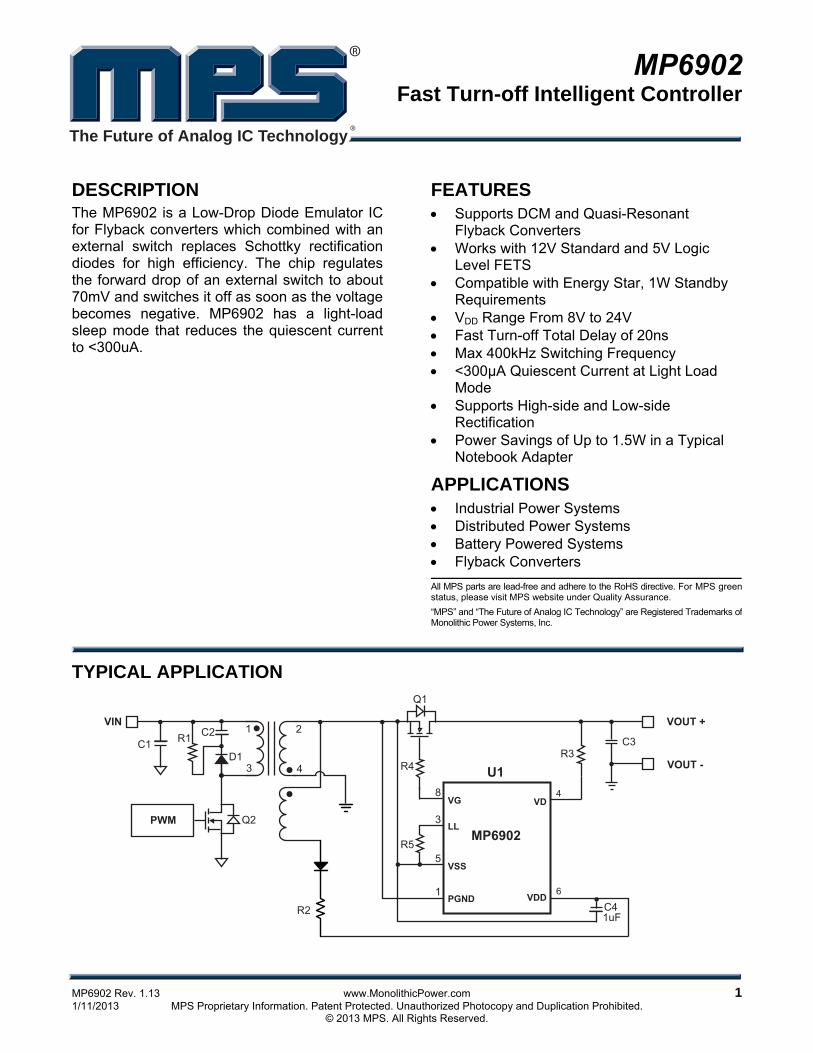
MP6902 Fast Turn-off Intelligent Controller MP6902 Rev. 1.13 www.MonolithicPower.com 1 1/11/2013 MPS Proprietary Information. Patent Protected. Unauthorized Photocopy and Duplication Prohibited. © 2013 MPS. All Rights Reserved. The Future of Analog IC Technology DESCRIPTION The MP6902 is a Low-Drop Diode Emulator IC for Flyback converters which combined with an external switch replaces Schottky rectification diodes for high efficiency. The chip regulates the forward drop of an external switch to about 70mV and switches it off as soon as the voltage becomes negative. MP6902 has a light-load sleep mode that reduces the quiescent current to <300uA. FEATURES • Supports DCM and Quasi-Resonant Flyback Converters • Works with 12V Standard and 5V Logic Level FETS • Compatible with Energy Star, 1W Standby Requirements • V DD Range From 8V to 24V • Fast Turn-off Total Delay of 20ns • Max 400kHz Switching Frequency • <300μA Quiescent Current at Light Load Mode • Supports High-side and Low-side Rectification • Power Savings of Up to 1.5W in a Typical Notebook Adapter APPLICATIONS • Industrial Power Systems • Distributed Power Systems • Battery Powered Systems • Flyback Converters All MPS parts are lead-free and adhere to the RoHS directive. For MPS green status, please visit MPS website under Quality Assurance. “MPS” and “The Future of Analog IC Technology” are Registered Trademarks of Monolithic Power Systems, Inc. TYPICAL APPLICATION
Transcript of MP6902 Fast Turn-off Intelligent...
MP6902 Fast Turn-off Intelligent Controller
MP6902 Rev. 1.13 www.MonolithicPower.com 1 1/11/2013 MPS Proprietary Information. Patent Protected. Unauthorized Photocopy and Duplication Prohibited. © 2013 MPS. All Rights Reserved.
The Future of Analog IC Technology
DESCRIPTION The MP6902 is a Low-Drop Diode Emulator IC for Flyback converters which combined with an external switch replaces Schottky rectification diodes for high efficiency. The chip regulates the forward drop of an external switch to about 70mV and switches it off as soon as the voltage becomes negative. MP6902 has a light-load sleep mode that reduces the quiescent current to <300uA.
FEATURES • Supports DCM and Quasi-Resonant
Flyback Converters • Works with 12V Standard and 5V Logic
Level FETS • Compatible with Energy Star, 1W Standby
Requirements • VDD Range From 8V to 24V • Fast Turn-off Total Delay of 20ns • Max 400kHz Switching Frequency • <300μA Quiescent Current at Light Load
Mode • Supports High-side and Low-side
Rectification • Power Savings of Up to 1.5W in a Typical
Notebook Adapter
APPLICATIONS • Industrial Power Systems • Distributed Power Systems • Battery Powered Systems • Flyback Converters All MPS parts are lead-free and adhere to the RoHS directive. For MPS green status, please visit MPS website under Quality Assurance. “MPS” and “The Future of Analog IC Technology” are Registered Trademarks of Monolithic Power Systems, Inc.
TYPICAL APPLICATION
MP6902- FAST TURN-OFF INTELLIGENT CONTROLLER
MP6902 Rev. 1.13 www.MonolithicPower.com 2 1/11/2013 MPS Proprietary Information. Patent Protected. Unauthorized Photocopy and Duplication Prohibited. © 2013 MPS. All Rights Reserved.
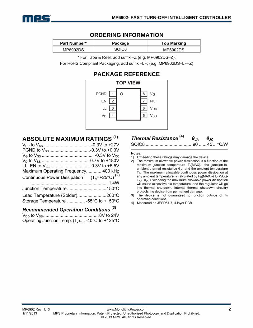
ORDERING INFORMATION Part Number* Package Top Marking
MP6902DS SOIC8 MP6902DS
* For Tape & Reel, add suffix –Z (e.g. MP6902DS–Z); For RoHS Compliant Packaging, add suffix –LF; (e.g. MP6902DS–LF–Z)
PACKAGE REFERENCE
PGND
EN
LL
VD
VG
NC
VDD
VSS
1
2
3
4
8
7
6
5
TOP VIEW
ABSOLUTE MAXIMUM RATINGS (1) VDD to VSS......................................-0.3V to +27V PGND to VSS ................................-0.3V to +0.3V VG to VSS ......................................... -0.3V to VCC VD to VSS .....................................-0.7V to +180V LL, EN to VSS ...............................-0.3V to +6.5V Maximum Operating Frequency............ 400 kHz Continuous Power Dissipation (TA=+25°C) (2) ............................................................. 1.4W Junction Temperature...............................150°C Lead Temperature (Solder).......................260°C Storage Temperature .............. -55°C to +150°C
Recommended Operation Conditions (3) VDD to VSS............................................8V to 24V Operating Junction Temp. (TJ).... -40°C to +125°C
Thermal Resistance (4) θJA θJC SOIC8 .....................................90 ...... 45 ... °C/W
Notes: 1) Exceeding these ratings may damage the device. 2) The maximum allowable power dissipation is a function of the
maximum junction temperature TJ(MAX), the junction-to-ambient thermal resistance θJA, and the ambient temperature TA. The maximum allowable continuous power dissipation at any ambient temperature is calculated by PD(MAX)=(TJ(MAX)-TA)/ θJA. Exceeding the maximum allowable power dissipation will cause excessive die temperature, and the regulator will go into thermal shutdown. Internal thermal shutdown circuitry protects the device from permanent damage.
3) The device is not guaranteed to function outside of its operating conditions.
4) Measured on JESD51-7, 4-layer PCB.
MP6902- FAST TURN-OFF INTELLIGENT CONTROLLER
MP6902 Rev. 1.13 www.MonolithicPower.com 3 1/11/2013 MPS Proprietary Information. Patent Protected. Unauthorized Photocopy and Duplication Prohibited. © 2013 MPS. All Rights Reserved.
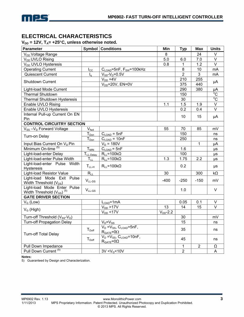
ELECTRICAL CHARACTERISTICS VDD = 12V, TA= +25°C, unless otherwise noted. Parameter Symbol Conditions Min Typ Max UnitsVDD Voltage Range 8 24 V VDD UVLO Rising 5.0 6.0 7.0 V VDD UVLO Hysteresis 0.8 1 1.2 V Operating Current ICC CLOAD=5nF, FSW=100kHz 8 10 mA Quiescent Current Iq VSS-VD=0.5V 2 3 mA
VDD =4V 210 255 Shutdown Current VDD=20V, EN=0V 375 440 µA
Light-load Mode Current 290 380 µA
Thermal Shutdown 150 oC Thermal Shutdown Hysteresis 30 oC Enable UVLO Rising 1.1 1.5 1.9 V
Enable UVLO Hysteresis 0.2 0.4 V Internal Pull-up Current On EN Pin 10 15 µA
CONTROL CIRCUITRY SECTION VSS –VD Forward Voltage Vfwd 55 70 85 mV
TDon CLOAD = 5nF 150 ns Turn-on Delay TDon CLOAD = 10nF 250 ns Input Bias Current On VD Pin VD = 180V 1 µA Minimum On-time (5) TMIN CLOAD = 5nF 1.6 µs Light-load-enter Delay TLL-Delay RLL=100kΩ 100 µs Light-load-enter Pulse Width TLL RLL=100kΩ 1.3 1.75 2.2 µs Light-load-enter Pulse Width Hysteresis TLL-H RLL=100kΩ 0.2 µs
Light-load Resistor Value RLL 30 300 kΩ Light-load Mode Exit Pulse Width Threshold (VDS) VLL-DS -400 -250 -150 mV
Light-load Mode Enter Pulse Width Threshold (VGS) (5) VLL-GS 1.0 V
GATE DRIVER SECTION VG (Low) ILOAD=1mA 0.05 0.1 V
VDD >17V 13 14 15 V VG (High) VDD <17V VDD-2.2 Turn-off Threshold (VSS-VD) 30 mV Turn-off Propagation Delay VD=VSS 15 ns
TDoff VD =VSS, CLOAD=5nF, RGATE=0Ω 35 ns
Turn-off Total Delay TDoff
VD =VSS, CLOAD=10nF, RGATE=0Ω 45 ns
Pull Down Impedance 1 2 Ω Pull Down Current (5) 3V <VG<10V 2 A
Notes: 5) Guaranteed by Design and Characterization.
MP6902- FAST TURN-OFF INTELLIGENT CONTROLLER
MP6902 Rev. 1.13 www.MonolithicPower.com 4 1/11/2013 MPS Proprietary Information. Patent Protected. Unauthorized Photocopy and Duplication Prohibited. © 2013 MPS. All Rights Reserved.
PIN FUNCTIONS
Pin # Name Description 1 PGND Power Ground, return for driver switch 2 EN Enable pin, active high 3 LL Light load timing setting. Connect a resistor to set the light load timing. 4 VD FET drain voltage sense 5 VSS Ground, also used as reference for VD 6 VDD Supply Voltage 7 NC No connection 8 VG Gate drive output
MP6902- FAST TURN-OFF INTELLIGENT CONTROLLER
MP6902 Rev. 1.13 www.MonolithicPower.com 5 1/11/2013 MPS Proprietary Information. Patent Protected. Unauthorized Photocopy and Duplication Prohibited. © 2013 MPS. All Rights Reserved.
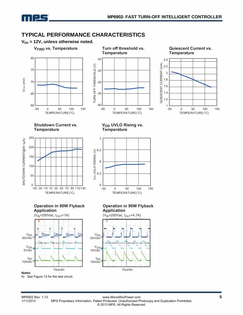
TYPICAL PERFORMANCE CHARACTERISTICS VDD = 12V, unless otherwise noted.
Notes: 6) See Figure 13 for the test circuit.
MP6902- FAST TURN-OFF INTELLIGENT CONTROLLER
MP6902 Rev. 1.13 www.MonolithicPower.com 6 1/11/2013 MPS Proprietary Information. Patent Protected. Unauthorized Photocopy and Duplication Prohibited. © 2013 MPS. All Rights Reserved.
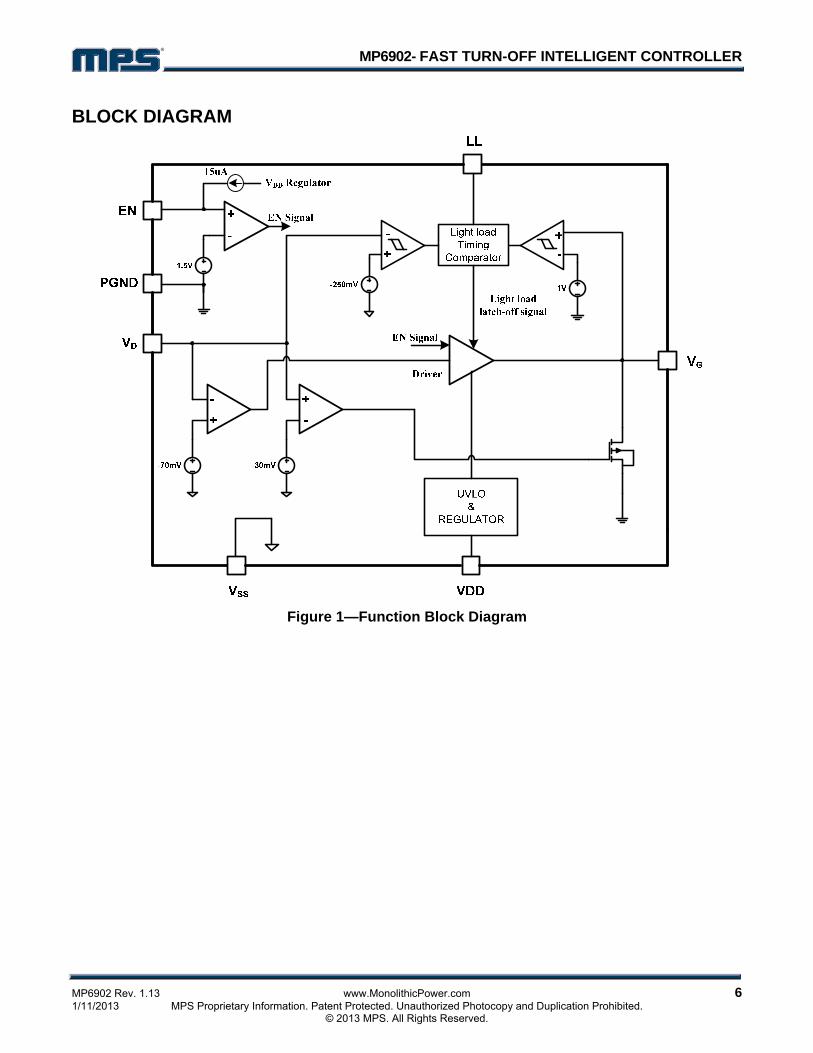
BLOCK DIAGRAM
Figure 1—Function Block Diagram
MP6902- FAST TURN-OFF INTELLIGENT CONTROLLER
MP6902 Rev. 1.13 www.MonolithicPower.com 7 1/11/2013 MPS Proprietary Information. Patent Protected. Unauthorized Photocopy and Duplication Prohibited. © 2013 MPS. All Rights Reserved.
OPERATION The MP6902 supports operation in DCM and Quasi-Resonant Flyback converters. The control circuitry controls the gate in forward mode and will turn the gate off when the MOSFET current is fairly low.
Blanking The control circuitry contains a blanking function. When it pulls the MOSFET on/off, it makes sure that the on/off state at least lasts for some time. The turn on blanking time is ~1.6us, which determines the minimum on-time. During the turn on blanking period, the turn off threshold is not totally blanked, but changes the threshold voltage to ~+50mV (instead of -30mV). This assures that the part can always be turned off even during the turn on blanking period. (Albeit slower)
VD Clamp Because VD can go as high as 180V, a High-Voltage JFET is used at the input. To avoid excessive currents when Vg goes below -0.7V, a small resistor is recommended between VD and the drain of the external MOSFET.
Under-Voltage Lockout (UVLO) When the VDD is below UVLO threshold, the part is in sleep mode and the Vg pin is pulled low by a 10kΩ resistor.
Enable pin If EN is pulled low, the part is in sleep mode.
Thermal shutdown If the junction temperature of the chip exceeds 170oC, the Vg will be pulled low and the part stops switching. The part will return to normal function after the junction temperature has dropped to 120oC.
Thermal Design If the dissipation of the chip is higher than 100mW due to switching frequencies above 100kHz.
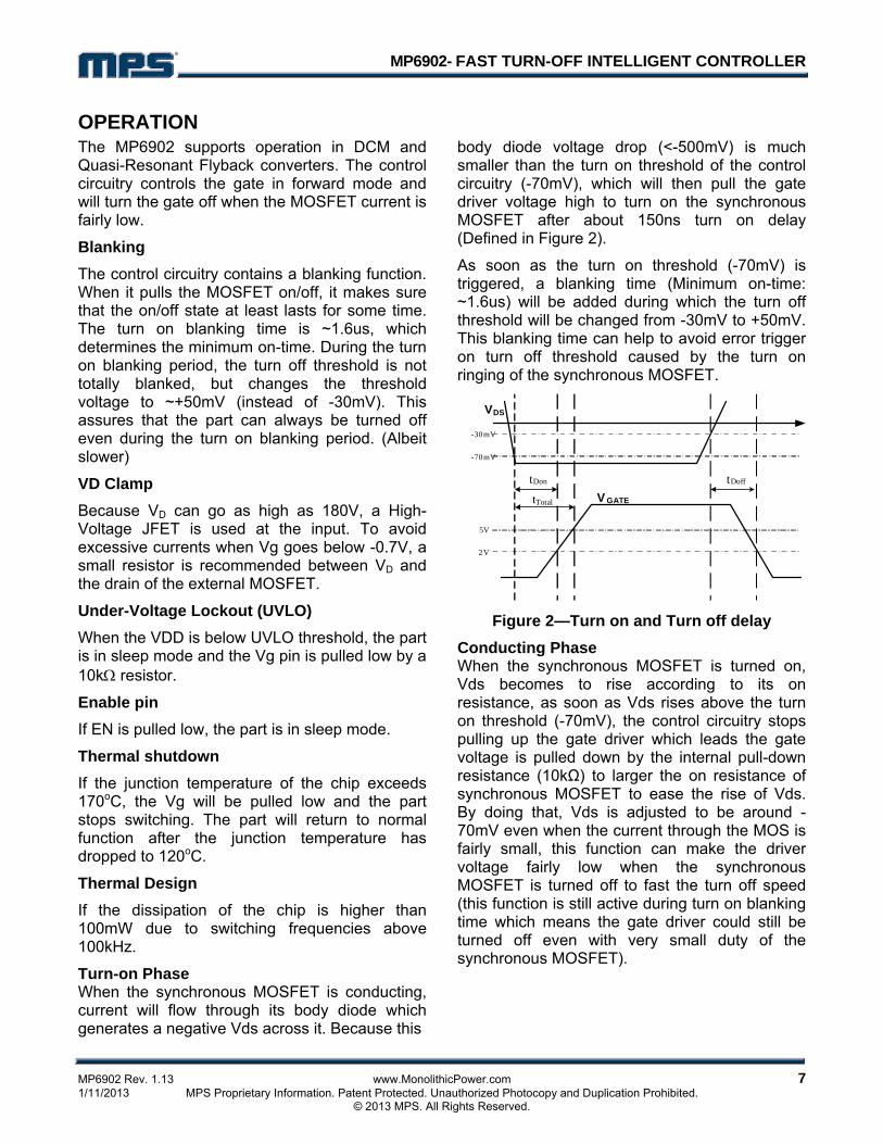
Turn-on Phase When the synchronous MOSFET is conducting, current will flow through its body diode which generates a negative Vds across it. Because this
body diode voltage drop (<-500mV) is much smaller than the turn on threshold of the control circuitry (-70mV), which will then pull the gate driver voltage high to turn on the synchronous MOSFET after about 150ns turn on delay (Defined in Figure 2).
As soon as the turn on threshold (-70mV) is triggered, a blanking time (Minimum on-time: ~1.6us) will be added during which the turn off threshold will be changed from -30mV to +50mV. This blanking time can help to avoid error trigger on turn off threshold caused by the turn on ringing of the synchronous MOSFET.
VDS
V GATE
tDon tDoff
-70mV
-30mV
2V
Totalt
5V
Figure 2—Turn on and Turn off delay Conducting Phase When the synchronous MOSFET is turned on, Vds becomes to rise according to its on resistance, as soon as Vds rises above the turn on threshold (-70mV), the control circuitry stops pulling up the gate driver which leads the gate voltage is pulled down by the internal pull-down resistance (10kΩ) to larger the on resistance of synchronous MOSFET to ease the rise of Vds. By doing that, Vds is adjusted to be around -70mV even when the current through the MOS is fairly small, this function can make the driver voltage fairly low when the synchronous MOSFET is turned off to fast the turn off speed (this function is still active during turn on blanking time which means the gate driver could still be turned off even with very small duty of the synchronous MOSFET).
MP6902- FAST TURN-OFF INTELLIGENT CONTROLLER
MP6902 Rev. 1.13 www.MonolithicPower.com 8 1/11/2013 MPS Proprietary Information. Patent Protected. Unauthorized Photocopy and Duplication Prohibited. © 2013 MPS. All Rights Reserved.
Turn-off Phase When Vds rises to trigger the turn off threshold (-30mV), the gate voltage is pulled to low after about 20ns turn off delay (defined in Figure 2) by the control circuitry. Similar with turn-on phase, a 200ns blanking time is added after the synchronous MOSFET is turned off to avoid error trigger.
Figure 3 shows synchronous rectification operation at heavy load condition. Due to the high current, the gate driver will be saturated at first, during which the gate driver voltage is kept at ~2V lower than VDD (when VDD>16V, gate driver will be internal clamped at 14V). After Vds goes to above -70mV, gate driver voltage decreases to adjust the Vds to typical -70mV.
Figure 4 shows synchronous rectification operation at light load condition. Due to the low current, the gate driver voltage never saturates but begins to decrease as soon as the synchronous MOSFET is turned on and adjust the Vds.
-70mV
-30mVVds
Isd
Vgst0 t1 t2
Figure 3—Synchronous Rectification Operation at heavy load
-70mV
-30mVVds
Isd
Vgst0 t1 t2
Figure 4—Synchronous Rectification Operation at light load
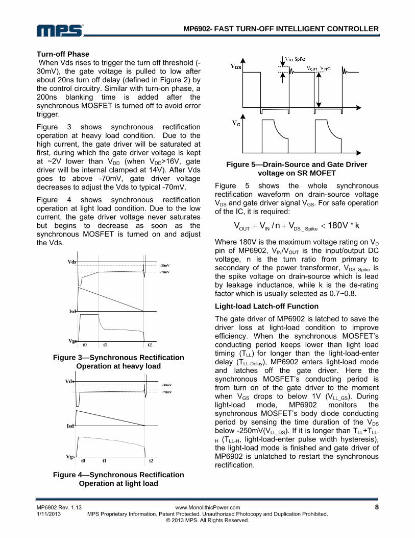
Figure 5—Drain-Source and Gate Driver
voltage on SR MOFET
Figure 5 shows the whole synchronous rectification waveform on drain-source voltage VDS and gate driver signal VGS. For safe operation of the IC, it is required:
OUT IN DS _ SpikeV V /n V 180V * k+ + <
Where 180V is the maximum voltage rating on VD pin of MP6902, VIN/VOUT is the input/output DC voltage, n is the turn ratio from primary to secondary of the power transformer, VDS_Spike is the spike voltage on drain-source which is lead by leakage inductance, while k is the de-rating factor which is usually selected as 0.7~0.8.
Light-load Latch-off Function The gate driver of MP6902 is latched to save the driver loss at light-load condition to improve efficiency. When the synchronous MOSFET’s conducting period keeps lower than light load timing (TLL) for longer than the light-load-enter delay (TLL-Delay), MP6902 enters light-load mode and latches off the gate driver. Here the synchronous MOSFET’s conducting period is from turn on of the gate driver to the moment when VGS drops to below 1V (VLL_GS). During light-load mode, MP6902 monitors the synchronous MOSFET’s body diode conducting period by sensing the time duration of the VDS below -250mV(VLL_DS). If it is longer than TLL+TLL-
H (TLL-H, light-load-enter pulse width hysteresis), the light-load mode is finished and gate driver of MP6902 is unlatched to restart the synchronous rectification.
MP6902- FAST TURN-OFF INTELLIGENT CONTROLLER
MP6902 Rev. 1.13 www.MonolithicPower.com 9 1/11/2013 MPS Proprietary Information. Patent Protected. Unauthorized Photocopy and Duplication Prohibited. © 2013 MPS. All Rights Reserved.
For MP6902, the light load enter timing (TLL) is programmable by connecting a resistor (RLL) on LL pin, by monitoring the LL pin current (the LL pin voltage keeps at ~2V internally), TLL is set as following:
LL LL2.2 sT R (k )
100kμ
≈ Ω ⋅Ω
SR MOSFET Selection and Driver Ability The Power Mosfet selection proved to be a trade off between Ron and Qg. In order to achieve high efficiency, the Mosfet with smaller Ron is always preferred, while the Qg is usually larger with smaller Ron, which makes the turn-on/off speed lower and lead to larger power loss. For MP6902, because Vds is regulated at ~-70mV during the driving period, the Mosfet with too small Ron is not recommend, because the gate driver may be pulled down to a fairly low level with too small Ron when the Mosfet current is still fairly high, which make the advantage of the low Ron inconspicuous.
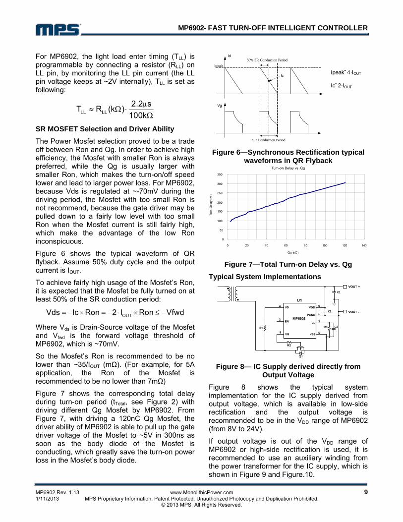
Figure 6 shows the typical waveform of QR flyback. Assume 50% duty cycle and the output current is IOUT.
To achieve fairly high usage of the Mosfet’s Ron, it is expected that the Mosfet be fully turned on at least 50% of the SR conduction period:
OUTVds Ic Ron 2 I Ron Vfwd= − × = − ⋅ × ≤ −
Where Vds is Drain-Source voltage of the Mosfet and Vfwd is the forward voltage threshold of MP6902, which is ~70mV.
So the Mosfet’s Ron is recommended to be no lower than ~35/IOUT (mΩ). (For example, for 5A application, the Ron of the Mosfet is recommended to be no lower than 7mΩ)
Figure 7 shows the corresponding total delay during turn-on period (tTotal, see Figure 2) with driving different Qg Mosfet by MP6902. From Figure 7, with driving a 120nC Qg Mosfet, the driver ability of MP6902 is able to pull up the gate driver voltage of the Mosfet to ~5V in 300ns as soon as the body diode of the Mosfet is conducting, which greatly save the turn-on power loss in the Mosfet’s body diode.
Id
Ipeak
Vg
SR Conduction Period
50% SR Conduction Period
IcIpeak˜ 4·IOUT
Ic˜ 2·IOUT
Figure 6—Synchronous Rectification typical
waveforms in QR Flyback Turn-on Delay vs. Qg
0
50
100
150
200
250
300
350
0 20 40 60 80 100 120 140
Qg (nC)
Tota
l Del
ay (
ns)
Figure 7—Total Turn-on Delay vs. Qg
Typical System Implementations
6
1
58
3
4
MP6902
R1 R3
C1
C2
C3
VD VDD
PGND
LL
VSSVG
EN
R2
2
Figure 8— IC Supply derived directly from Output Voltage
Figure 8 shows the typical system implementation for the IC supply derived from output voltage, which is available in low-side rectification and the output voltage is recommended to be in the VDD range of MP6902 (from 8V to 24V).
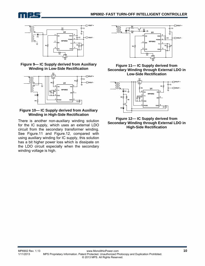
If output voltage is out of the VDD range of MP6902 or high-side rectification is used, it is recommended to use an auxiliary winding from the power transformer for the IC supply, which is shown in Figure 9 and Figure.10.
MP6902- FAST TURN-OFF INTELLIGENT CONTROLLER
MP6902 Rev. 1.13 www.MonolithicPower.com 10 1/11/2013 MPS Proprietary Information. Patent Protected. Unauthorized Photocopy and Duplication Prohibited. © 2013 MPS. All Rights Reserved.
6
1
R3
58
3
C3
4
MP6902
C2
R1
R2
R4 C1
D1 VD VDD
PGND
LL
VSSVG
EN2
Figure 9— IC Supply derived from Auxiliary Winding in Low-Side Rectification
R1
R2
R3C3
R4 C2
C1
D1
VD
VSS
LL
VG
PGND VDD
EN 2MP6902
1
3
5
8 4
6
Figure 10— IC Supply derived from Auxiliary Winding in High-Side Rectification
There is another non-auxiliary winding solution for the IC supply, which uses an external LDO circuit from the secondary transformer winding. See Figure.11 and Figure.12, compared with using auxiliary winding for IC supply, this solution has a bit higher power loss which is dissipate on the LDO circuit especially when the secondary winding voltage is high.
6
1
R3
58
3
3C
4
MP6902
2C
R4
R5D1
D21C
R1
R2
PGND
VDD
2LL
VSS
VD
EN
VG
Figure 11— IC Supply derived from Secondary Winding through External LDO in
Low-Side Rectification
R4R5
D1
D2 C2
C1R1
R2
R3C3
MP6902VG
LL
VSS
PGND VDD
VD
2EN
1 6
3
5
48
Figure 12— IC Supply derived from Secondary Winding through External LDO in
High-Side Rectification
MP6902- FAST TURN-OFF INTELLIGENT CONTROLLER
MP6902 Rev. 1.13 www.MonolithicPower.com 11 1/11/2013 MPS Proprietary Information. Patent Protected. Unauthorized Photocopy and Duplication Prohibited. © 2013 MPS. All Rights Reserved.
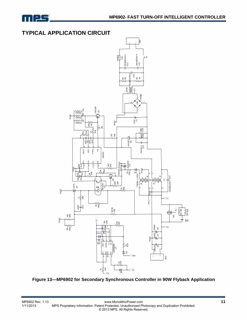
TYPICAL APPLICATION CIRCUIT
Figure 13—MP6902 for Secondary Synchronous Controller in 90W Flyback Application
MP6902- FAST TURN-OFF INTELLIGENT CONTROLLER
NOTICE: The information in this document is subject to change without notice. Users should warrant and guarantee that third party Intellectual Property rights are not infringed upon when integrating MPS products into any application. MPS will not assume any legal responsibility for any said applications.
MP6902 Rev. 1.13 www.MonolithicPower.com 12 1/11/2013 MPS Proprietary Information. Patent Protected. Unauthorized Photocopy and Duplication Prohibited. © 2013 MPS. All Rights Reserved.
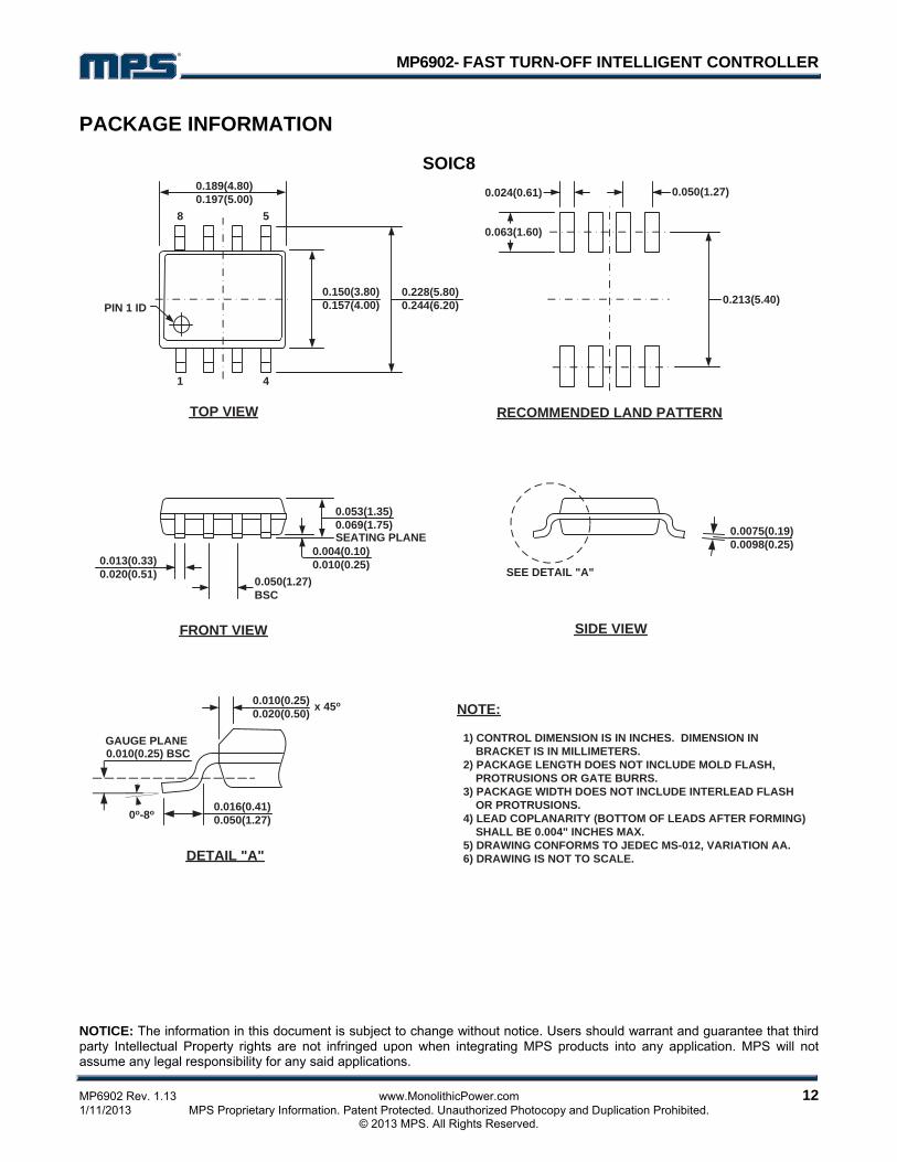
PACKAGE INFORMATION
SOIC8
0.016(0.41)0.050(1.27)0o-8o
DETAIL "A"
0.010(0.25)0.020(0.50) x 45o
SEE DETAIL "A"
0.0075(0.19)0.0098(0.25)
0.150(3.80)0.157(4.00)PIN 1 ID
0.050(1.27)BSC
0.013(0.33)0.020(0.51)
SEATING PLANE0.004(0.10)0.010(0.25)
0.189(4.80)0.197(5.00)
0.053(1.35)0.069(1.75)
TOP VIEW
FRONT VIEW
0.228(5.80)0.244(6.20)
SIDE VIEW
1 4
8 5
RECOMMENDED LAND PATTERN
0.213(5.40)
0.063(1.60)
0.050(1.27)0.024(0.61)
NOTE:
1) CONTROL DIMENSION IS IN INCHES. DIMENSION IN BRACKET IS IN MILLIMETERS. 2) PACKAGE LENGTH DOES NOT INCLUDE MOLD FLASH, PROTRUSIONS OR GATE BURRS. 3) PACKAGE WIDTH DOES NOT INCLUDE INTERLEAD FLASH OR PROTRUSIONS. 4) LEAD COPLANARITY (BOTTOM OF LEADS AFTER FORMING) SHALL BE 0.004" INCHES MAX. 5) DRAWING CONFORMS TO JEDEC MS-012, VARIATION AA. 6) DRAWING IS NOT TO SCALE.
0.010(0.25) BSCGAUGE PLANE