MP COMPLETE NOTES - BPUTold.bput.ac.in/lecture_notes/Microprocessor_5th semester_ ETC_PCEC... ·...
101
MODULE 1 TOPICS COVERED:- 1. Introduction to the general concept of microprocessor 2. I/O subsystem , programming the system 3. ALU 4. Instruction execution, instruction word format 5. Addressing modes 6. Address/data/control bus 7. Tristate bus 8. Interfacing i/o device 9. Data transfer scheme 10. Architectural advancement of microprocessor 11. Evolution of processor INTRODUCTION A computer basically consists of the following parts:- 1. I/O devices 2. Memory 3. CPU The CPU is the brain of the computer irrespective of its size. The CPU normally consists of a large scale integrationcircuit called Microprocessor and works as central processing unit of a microcomputer. Input Devices give data or information as an input to the CPU and it processes the data or information given by the devices. Memory stores the data or information, Output Devices give the required data as output to the user. A digital component in which one microprocessor has been provided to act as a CPU is known as Microcomputer. Desktop computer, laptop computer, palm computer, notebook are the ones which contain only one microprocessor to act as a CPU. Microprocessor:- Definition- A microprocessor is a multipurpose programmable, clock driven, semiconductor device consisting of electronic logic circuit manufactured by using very large scale integration (VLSI) technique. • The Microprocessor is capable of performing various computing functions and making decisions to change the sequence of program executions.
Transcript of MP COMPLETE NOTES - BPUTold.bput.ac.in/lecture_notes/Microprocessor_5th semester_ ETC_PCEC... ·...

MODULE 1
TOPICS COVERED:-
1. Introduction to the general concept of microprocessor
2. I/O subsystem , programming the system
3. ALU
4. Instruction execution, instruction word format
5. Addressing modes
6. Address/data/control bus
7. Tristate bus
8. Interfacing i/o device
9. Data transfer scheme
10. Architectural advancement of microprocessor
11. Evolution of processor
INTRODUCTION A computer basically consists of the following parts:-
1. I/O devices
2. Memory
3. CPU
The CPU is the brain of the computer irrespective of its size. The CPU normally consists of a large
scale integrationcircuit called Microprocessor and works as central processing unit of a
microcomputer.
Input Devices give data or information as an input to the CPU and it processes the data or
information given by the devices. Memory stores the data or information, Output Devices give the
required data as output to the user.
A digital component in which one microprocessor has been provided to act as a CPU is known as
Microcomputer. Desktop computer, laptop computer, palm computer, notebook are the ones which
contain only one microprocessor to act as a CPU.
Microprocessor:-
Definition- A microprocessor is a multipurpose programmable, clock driven, semiconductor device
consisting of electronic logic circuit manufactured by using very large scale integration (VLSI)
technique.
• The Microprocessor is capable of performing various computing functions and making
decisions to change the sequence of program executions.
• The microprocessor application are classified primarily into two categories:-
1. Reprogrammable systems
2. Embedded System
• Microprocessor can perform the following operations:-
1. Read data from memory
2. Write data into memory
3. Accept data from input devices
4. Sends data to output devices
5. Data processing
6. Arithmetic and logic operations
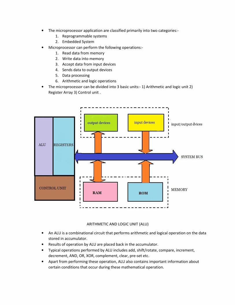
• The microprocessor can be divided into 3 basic units:- 1) Arithmetic and logic unit 2)
Register Array 3) Control unit .
ARITHMETIC AND LOGIC UNIT (ALU)
• An ALU is a combinational circuit that performs arithmetic and logical operation on the data
stored in accumulator.
• Results of operation by ALU are placed back in the accumulator.
• Typical operations performed by ALU includes add, shift/rotate, compare, increment,
decrement, AND, OR, XOR, complement, clear, pre-set etc.
• Apart from performing these operation, ALU also contains important information about
certain conditions that occur during these mathematical operation.
• These conditions i.e. occurrence of carry, borrow, zero, negative or even parity results are
stored in register called flag register and the individual bits are called flag bits.
• The number of bits is the most important factor determining the capabilities of the
processor. Hence the size of ALU defines the size of the microprocessor.
Instruction Execution The microprocessor performs operations by accepting instructions from the user. Every
program consists of a sequence of instructions. The commands of n instruction set are called
‘mnemonics’. A command is understood by the CPU only when it is converted into
equivalent single byte hexadecimal opcodes with or without one-byte or two byte data or
address.
An instruction consists of:-
1. Opcode (operational code)
2. Operand(Operational End)
Instruction Data Format
1. Every microprocessor has a different of instruction data format. The instruction format of each
microprocessor depends upon its address, data and control bus.
2. Every instruction contains an operand and an opcode.
3. In typical microprocessor is organized in 8 bits, each of which has unique memory location in the
physical memory. Each memory is specified by a 16 bit hexadecimal address.
4. Data is stored in the memory as 8 bit binary number arrangement of 8 bits of a stored data s
shown below:
5. Instruction stored in first byte must be the opcode.
6. Instruction can be categorized in 3 parts:
1) One-byte instruction/ one word instruction
2) Two-byte instruction/two word instruction
3) Three-byte instruction/three word instruction
� ONE BYTE INSTRUCTION:
This type of instruction requires one memory location. The 8 bit or 1 byte instruction code is called as
opcodes that uniquely identifies the instruction. If the instruction is one byte then the timing diagram
has only one machine cycle i.e. opcode fetch cycle. it has only one opcode.
EX- CMA; MOV A,B; ADD C; SUB D; RLC .

� TWO BYTE INSTRUCTION:
In this kind of instruction, the first byte is for the opcode and the second byte is for the operand or the
code associated with the memory address. such instructions are stored in two consecutive memory
locations. if the instruction is two byte, then it requires two machine cycle. The first machine cycle is for
opcode fetch and the second machine cycle is either for memory read/memory write i/o read or i/o
write.
EX: MVI B,62; ADI 58; ORI 43; IN 89.
� THREE BYTE INSTRUCTION:
In this type of instruction, the first byte is for opcode and the second and third byte is for an operand
code associated with the memory address. Such instructions are stored in 3 consecutive memory
locations. If the instruction is of three bytes, then it requires three machine cycles. The first machine
cycle is for opcode fetch and the second and third machine cycle is either for memory read/memory
write I/O read or I/O write.
EX: LDA 8062; LXI H, 8057; JMP 7809.
� Instruction format
Intel 8085 handles 8 bit of data as it is an 8 bit microprocessor. It is designed to process 8 bit of data at a
time. If a 16 bit data has to be stored then they are stored in consecutive memory locations.
There are various ways to specify data for an instruction:
� 8 bit or 16 bit data may be directly given in the instruction. E.g. ADI 07H, LXI 7051H etc.
� The address of the memory location or I/O devices may be given in the instruction itself. Ex LDA
8582H, IN 02H etc.
� In some instructions only one register is specified. Ex ADD B
� In some instructions we write two registers. Ex MOV D,E
� In some instructions the data is implicit or implied. Ex CMA, RRC, RAL.
Addressing Modes
Addressing modes are an asset of the instruction set architecture in most CPU designs. The
various addressing modes that are defined in a given instruction set architecture define how
machine language instructions in that architecture identity the operand of each instruction. An
addressing mode specifies how to calculate the effective memory address of an operand by
using information held in register and/or constants contained within machine instruction or
elsewhere.
. For 8085 there are five addressing modes. They are:
� DIRECT ADDRESSING MODE
In type of addressing mode the address of the operand or the data is given to the instruction itself. This
type of mode is used to accept data from outside devices to store the data in the accumulator and send
the data stored in the accumulator to the output devices.
E.g. IN 02 (to accept the data from the port 02h and store the same in the accumulator)
OUT 01H (send the data from the accumulator to the output port)
LHLD address (load H-L pair direct.)
� REGISTER ADDRESSING MODE
In type of addressing mode the address is provided through the registers. Here the operand is GPR.
E.g. MOV Rd,Rs (move a copy of data from the source register to the destination register)
ADD B (add the content of b to the accumulator and the value is stored in the accumulator)
INR C (Increment the value of the register c by 1)
� REGISTER INDIRECT ADDRESSING MODE
In type of addressing mode the address of the operand or the data is specified by a pair of register
before the execution of the instruction itself. Here the address of the memory is not directly given in the
instruction. The address of the memory resides in H-L pair and this has been already specified in an
earlier instruction.
E.g. LXI H, 8175; MOV B, M (move the data from memory specified by H-l pair to the register b)
LXI H, 8763; ADD M (Add the content of memory specified of the H-L pair to the accumulator)
� IMMEDIATE ADDRESSING MODE
in type of addressing mode the data is directly associated in the instruction itself. It loads immediate
data to the destination provided in the instruction.
E.g. MVI r. D8 (move an 8 it data directly to the register)
ADI 62H (add 62 to the accumulator content and store the result in the accumulator)
JMP address, JC address, CPI D8.
� IMPLICIT ADDRESSING MODE
There are certain instruction which are operated on the content of the accumulator. These types of
construction don’t require any address of the operand.
Eg. CMA (it finds the 1’s compliment of the data present in the accumulator and stores in accumulator)

RAL (rotate the content of accumulator left through carry)
RRC (rotate the content of accumulator right without carry)
Various Input or Output devices and memory devices are connected to the CPU by a group of
conductors i.e. copper wires called buses. A typical microprocessor communicates with memory
and other I/O devices using 3 busses such as:
Address Bus:-
It carries the address of memory location or I/O devices that the CPU wants to access. When an
address is sent by the CPU, all devices connected to CPU through it receives the address but only
that device will respond which has also received t
bus is Unidirectional i.e. address can send by microprocessor only. The number of memory
location that can be addressed by the CPU is determined by the number of address lines.
Data Bus:-
Data Buses are Bi-directional. The control can read data from memory or an input port and also
write data to memory or output port. Many devices have their output ports connected to data
bus, but only those respond whose enable signal is high.
Control bus:-
Control buses, like data buses are bi
signal lines. The CPU sends out signals on the control bus to enable the outputs of addressed
memory devices and port devices. The basic types of signals are, memory read (MR), memo
(MW), Input and Output read (IOR) and Input and output write (IOW). To read a byte from
memory, the CPU sends out the address of memory location through address bus and then
sends read signal to the device through the control bus.
RAL (rotate the content of accumulator left through carry)
RRC (rotate the content of accumulator right without carry)
BUS Structure
put devices and memory devices are connected to the CPU by a group of
conductors i.e. copper wires called buses. A typical microprocessor communicates with memory
and other I/O devices using 3 busses such as: - 1) Address bus 2) Data Bus 3) Control Bus
It carries the address of memory location or I/O devices that the CPU wants to access. When an
address is sent by the CPU, all devices connected to CPU through it receives the address but only
that device will respond which has also received the chip enable signal from CPU. The address
bus is Unidirectional i.e. address can send by microprocessor only. The number of memory
location that can be addressed by the CPU is determined by the number of address lines.
ional. The control can read data from memory or an input port and also
write data to memory or output port. Many devices have their output ports connected to data
bus, but only those respond whose enable signal is high.
ata buses are bi-directional. The control bus consists of 4 to 10 parallel
signal lines. The CPU sends out signals on the control bus to enable the outputs of addressed
memory devices and port devices. The basic types of signals are, memory read (MR), memo
(MW), Input and Output read (IOR) and Input and output write (IOW). To read a byte from
memory, the CPU sends out the address of memory location through address bus and then
sends read signal to the device through the control bus.
put devices and memory devices are connected to the CPU by a group of
conductors i.e. copper wires called buses. A typical microprocessor communicates with memory
1) Address bus 2) Data Bus 3) Control Bus
It carries the address of memory location or I/O devices that the CPU wants to access. When an
address is sent by the CPU, all devices connected to CPU through it receives the address but only
he chip enable signal from CPU. The address
bus is Unidirectional i.e. address can send by microprocessor only. The number of memory
location that can be addressed by the CPU is determined by the number of address lines.
ional. The control can read data from memory or an input port and also
write data to memory or output port. Many devices have their output ports connected to data
directional. The control bus consists of 4 to 10 parallel
signal lines. The CPU sends out signals on the control bus to enable the outputs of addressed
memory devices and port devices. The basic types of signals are, memory read (MR), memory
(MW), Input and Output read (IOR) and Input and output write (IOW). To read a byte from
memory, the CPU sends out the address of memory location through address bus and then
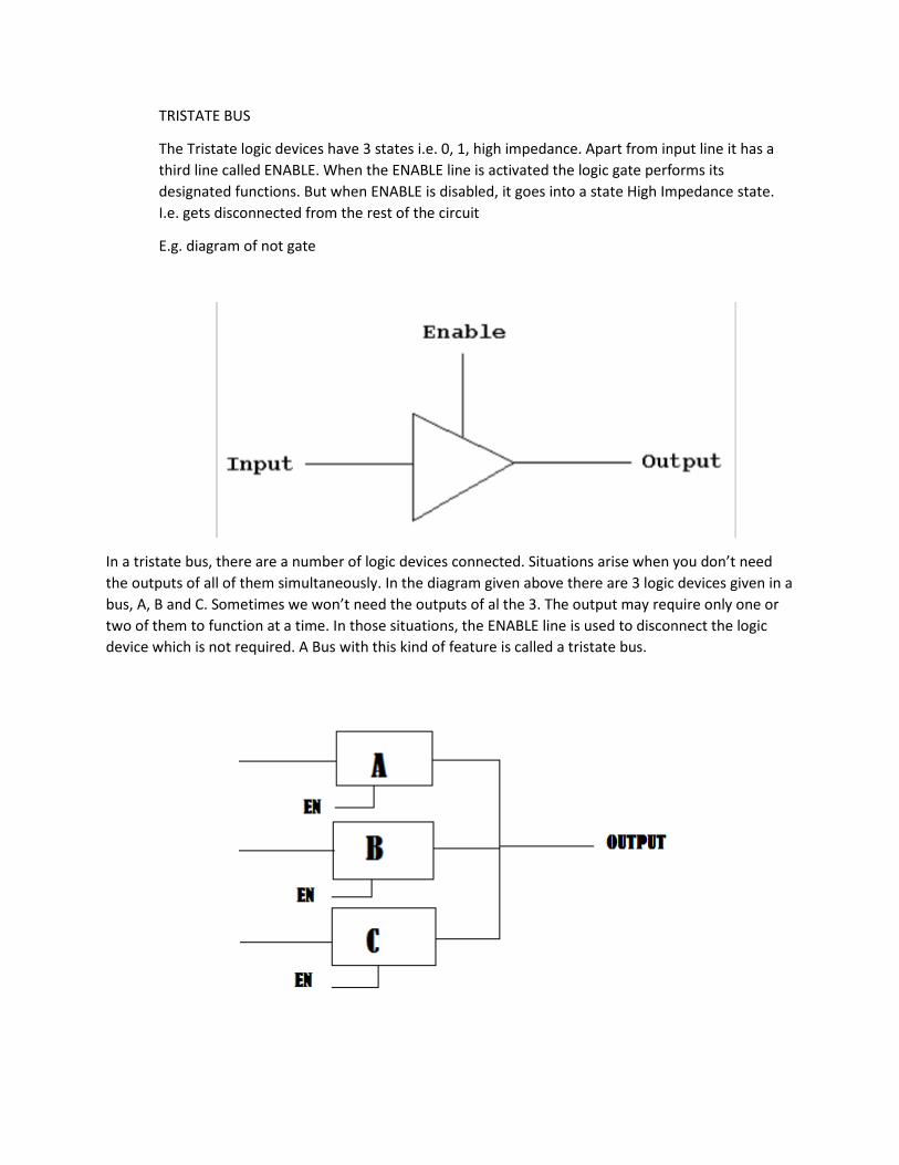
TRISTATE BUS
The Tristate logic devices have 3 states i.e. 0, 1, high impedance. Apart from input line it has a
third line called ENABLE. When the ENABLE line is activated the logic gate performs its
designated functions. But when ENABLE is disabled, it goes into a state High
I.e. gets disconnected from the rest of the circuit
E.g. diagram of not gate
In a tristate bus, there are a number of logic devices connected. Situations arise when you don’t need
the outputs of all of them simultaneously. In the diagra
bus, A, B and C. Sometimes we won’t need the outputs of al the 3. The output may require only one or
two of them to function at a time. In those situations, the ENABLE line is used to disconnect the logic
device which is not required. A Bus with this kind of feature is called a tristate bus.
tate logic devices have 3 states i.e. 0, 1, high impedance. Apart from input line it has a
third line called ENABLE. When the ENABLE line is activated the logic gate performs its
designated functions. But when ENABLE is disabled, it goes into a state High Impedance state.
I.e. gets disconnected from the rest of the circuit
In a tristate bus, there are a number of logic devices connected. Situations arise when you don’t need
the outputs of all of them simultaneously. In the diagram given above there are 3 logic devices given in a
bus, A, B and C. Sometimes we won’t need the outputs of al the 3. The output may require only one or
two of them to function at a time. In those situations, the ENABLE line is used to disconnect the logic
device which is not required. A Bus with this kind of feature is called a tristate bus.
tate logic devices have 3 states i.e. 0, 1, high impedance. Apart from input line it has a
third line called ENABLE. When the ENABLE line is activated the logic gate performs its
Impedance state.
In a tristate bus, there are a number of logic devices connected. Situations arise when you don’t need
m given above there are 3 logic devices given in a
bus, A, B and C. Sometimes we won’t need the outputs of al the 3. The output may require only one or
two of them to function at a time. In those situations, the ENABLE line is used to disconnect the logic
ENABLE
0
1
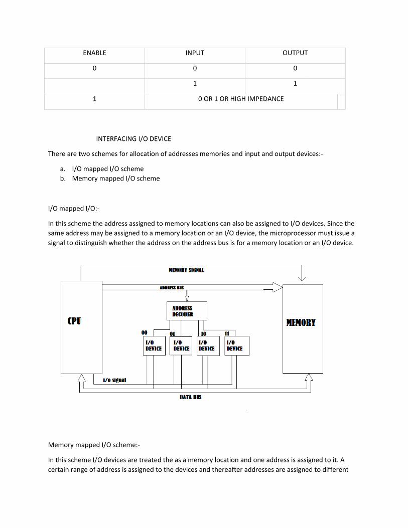
INTERFACING I/O DEVICE
There are two schemes for allocation of addresses memories and input and
a. I/O mapped I/O scheme
b. Memory mapped I/O scheme
I/O mapped I/O:-
In this scheme the address assigned to memory locations can also be assigned to I/O devices. Since the
same address may be assigned to a memory location or an I/O device, the
signal to distinguish whether the address on the address bus is for a memory location or an I/O device.
Memory mapped I/O scheme:-
In this scheme I/O devices are treated the as a memory location and one address is assigned t
certain range of address is assigned to the devices and thereafter addresses are assigned to different
INPUT OUTPUT
0 0
1 1
0 OR 1 OR HIGH IMPEDANCE
INTERFACING I/O DEVICE
There are two schemes for allocation of addresses memories and input and output devices:
Memory mapped I/O scheme
In this scheme the address assigned to memory locations can also be assigned to I/O devices. Since the
same address may be assigned to a memory location or an I/O device, the microprocessor must issue a
signal to distinguish whether the address on the address bus is for a memory location or an I/O device.
In this scheme I/O devices are treated the as a memory location and one address is assigned t
certain range of address is assigned to the devices and thereafter addresses are assigned to different
OUTPUT
output devices:-
In this scheme the address assigned to memory locations can also be assigned to I/O devices. Since the
microprocessor must issue a
signal to distinguish whether the address on the address bus is for a memory location or an I/O device.
In this scheme I/O devices are treated the as a memory location and one address is assigned to it. A
certain range of address is assigned to the devices and thereafter addresses are assigned to different
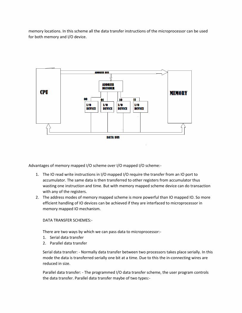
memory locations. In this scheme all the data transfer instructions of the microprocessor can be used
for both memory and I/O device.
Advantages of memory mapped I/O scheme over I/O mapped I/O scheme:
1. The IO read write instructions in I/O mapped I/O require the transfer from an IO port to
accumulator. The same data is then transferred to other registers from accumulator thus
wasting one instruction and time. But with memory mapped scheme device can do transaction
with any of the registers.
2. The address modes of memory mapped scheme is more powerful than IO mapped IO. So more
efficient handling of IO devices can be achieved if they are interface
memory mapped IO mechanism.
DATA TRANSFER SCHEMES:
There are two ways by which we can pass data to microprocessor:
1. Serial data transfer
2. Parallel data transfer
Serial data transfer: - Normally data transfer between two processors
mode the data is transferred serially one bit at a time. Due to this the in
reduced in size.
Parallel data transfer: - The programmed I/O data transfer scheme, the user program controls
the data transfer. Parallel data transfer maybe of two types:
memory locations. In this scheme all the data transfer instructions of the microprocessor can be used
ages of memory mapped I/O scheme over I/O mapped I/O scheme:-
The IO read write instructions in I/O mapped I/O require the transfer from an IO port to
accumulator. The same data is then transferred to other registers from accumulator thus
uction and time. But with memory mapped scheme device can do transaction
The address modes of memory mapped scheme is more powerful than IO mapped IO. So more
efficient handling of IO devices can be achieved if they are interfaced to microprocessor in
memory mapped IO mechanism.
DATA TRANSFER SCHEMES:-
There are two ways by which we can pass data to microprocessor:-
Normally data transfer between two processors takes place serially. In this
mode the data is transferred serially one bit at a time. Due to this the in-connecting wires are
The programmed I/O data transfer scheme, the user program controls
Parallel data transfer maybe of two types:-
memory locations. In this scheme all the data transfer instructions of the microprocessor can be used
The IO read write instructions in I/O mapped I/O require the transfer from an IO port to
accumulator. The same data is then transferred to other registers from accumulator thus
uction and time. But with memory mapped scheme device can do transaction
The address modes of memory mapped scheme is more powerful than IO mapped IO. So more
d to microprocessor in
takes place serially. In this
connecting wires are
The programmed I/O data transfer scheme, the user program controls

1. Synchronous: - This type of data transfer is used when device which sends data and devices
which receives data are synchronised with the same clock. Works when IO devices and the
CPU works with the same speed. IN/OUT instructions are used to transfer data from IO
devices to memory and vice versa. Generally used in IO mapped IO scheme, can also be used
with memory mapped IO scheme with proper memory read/write instruction. Data is
transferred as soon as CPU gives instruction to do so. There is no need to check if the device
is ready or not.
2. Asynchronous: - It means at “regular intervals”. This type of data transfer scheme is used
when speed of the IO device does not match with that of CPU. There is no predictability of
timing characteristics. The microprocessor always pings the other device to check whether
it’s ready or not. During initiation the CPU checks whether device is ready to transfer data,
before the actual transfer of data the memory keeps sending signal to IO device. This is
called handshaking. The CPU sends initialising signal to device during start and after actual
data transfer.
Interrupt Data transfer scheme: - The program initiates the program and then executes the
main program. When IO device is ready to transfer data, the interrupt signal becomes high.
The CPU completes the task at hand and then it attends to the IO device. It transfers the
data to the stack and then executes a subroutine called ISS (interrupt Service Subroutine).
ISS execution transfers data from IO device to memory and vice versa.
Direct memory access: - For bulk transfer to or from IO device the above mentioned
techniques might prove inefficient. So DMA process is ideal for transferring huge amount of
data. The IO device requests the microprocessor by sending a signal. After receiving this
request signal the CPU disconnects itself from memory and IO devices by tristating address,
data and control bus. The CPU sends the acknowledge signal to IO device. After this data
transfer takes place, and on completion IO device withdraws DMA request.
Advancement of architecture of microprocessor
1. Cache memory: - To speed up execution of data, a buffer between the CPU and memory
is used. It consists of high speed static ram. Execution speed is equal to microprocessor
speed.
2. Pipelining:- This is used to speed up execution of instruction. While the execution unit is
working on instructions, the queue in a CPU fetches the next set of instructions. As soon
as the working on instruction is over, the next set of instructions are fed into the
execution unit. There is no time wasted in fetching instructions. This technique is called
pipelining.
3. Multitasking or memory management: - Due to growth in hardware complexity of
computers, they were used in time sharing working environment. That means a fixed
amount of time is allocated to different programmes. To achieve relocatablity
segmented scheme is used.
4. Virtual memory system:- In this scheme the complete program is divided into several
pgs. and stored in hard disk. At same time the main memory is divided into small pages.
By this we can swap the pages between hard disk and main memory. This task is
performed by the operating system. Main memory size is bigger than physical memory
size which is correct.
EVOLUTION OF MICROPROCESSORS
� FIRST GENERATION :
The first microprocessor is intel 4004. PMOS microprocessor introduced in he year 1971 nt the intel
corporation, USA. The enhanced version of this is intel 4040. Memory addressing capacity is 1kb, clock
frequency is 750 khz. No of pins is 16 and clock freq is defined as the no instruction that can be executed
in one sec.
Other eg. Rockwell international’s PPS-4, TOSHIBA t3472 etc
� SECOND GENERATION
The first 8 bit is microprocessor is intel 8008 introduced in the year 1972 which is a 8 bit
pmosmicroprocessor .in the year 1973, intel 8080 which is an 8 bit, nmos microprocessor was in
traduced which is faster and compatible to TTL than that of pmos technology. But intel 8080 requires
three power supplies so in the year 1975 intel 8085 , an 8 bit nmos microprocessor was introduced
which requires one power supply ie +5v dc. Memory addressing : -64 kb , clock frequency – 1mhz to
6mhz. No of pins 40.
Other eg. Rockwell international’s PPS 8, ZILOG’s z-800 etc
� THIRD GENERATION
In 1975, a 16 bit microprocessor was developed which is anhmos microprocessor. Memory addressing
capacity: i mb to 16 mb, clock frequency 6 to 12.5 mhz, no of pins -40
Other eg. Intel 8088, 80186, 80286
Intel 80186 and 80188 are integrated microprocessors beside cpu. They contain some additional
components that are PIC, DMA, PC Or timer, clock generator, peripheral chip select logic. Programmable
state generator and local bus controller etc. In intel 80286 besides cpu it has integrated memory
management unit, four level memory protections, it supports virtual memory and operating systems.
� FOURTH GENERATION
After 1980, 32 bit microprocessors were produced. The first 32 bit microprocessor is iAPX 432. This is
not popular as it is eventually disconnected. The most powerful and very popular 32 bit microprocessor
is intel 80386. In short it is called intel-386. Memory addressing capacity 4gb, clock frequency-20 mhz to
in ghz. No of pins is 132 or more.
Ohereg. Pentium pro, Pentium II xenon, Pentium II celerum , Pentium III.
MODULE -2
INTEL 8086- HARDWARE ARCHITECTURE
INTRODUCTION:-
LIMITATION OF 8 BIT MICROPROCESSORS:
1. LOW SPEED OF EXICUTION
2. LOW MEMORY ADDRESSING CAPABILITY
3. LIMITED NUMBER OF GENERAL PURPOSE REGISTERS
4. LESS POWERFUL INSTRUCTION SET.
NOTE: - All these limitation of these 8 bit microprocessors were being over carried by a new
powerful output of 8086.
FEATURES OF 8086:
1. The 8086 is a 16-bit N-channel, H-MOS Microprocessor.
2. It’s CMOS version is available in “80C86”
3. It consumes less power.
4. It is introduced in 1978
5. It contains an electronic circuit of 29000 transistors
6. It is built on a single semiconductor chip and packaged in 40-pin IC packing.
7. It has 20 address lines and 16 data lines
8. It can directly address up to 220, , which is nearly equal to 1M bytes of memory
9. It has 16 bit registers for symmetrical operations
10. It has 24 operand addressing mode
11. It can support 8 &16 bit signed and unsigned arithmetic in binary or decimal
12. Multi bus compatible system interface. etc.
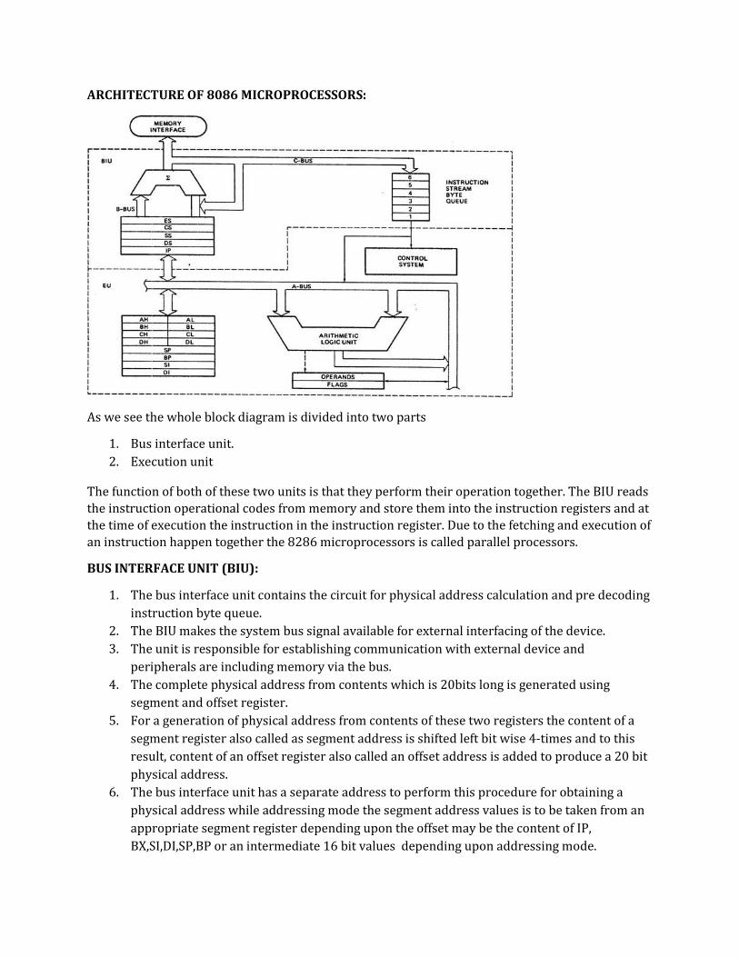
ARCHITECTURE OF 8086 MICROPROCESSORS:
As we see the whole block diagram is divided into two parts
1. Bus interface unit.
2. Execution unit
The function of both of these two units is that they perform their operation together. The BIU reads
the instruction operational codes from memory and store them into the instruction registers and at
the time of execution the instruction in the instruction register. Due to the fetching and execution of
an instruction happen together the 8286 microprocessors is called parallel processors.
BUS INTERFACE UNIT (BIU):
1. The bus interface unit contains the circuit for physical address calculation and pre decoding
instruction byte queue.
2. The BIU makes the system bus signal available for external interfacing of the device.
3. The unit is responsible for establishing communication with external device and
peripherals are including memory via the bus.
4. The complete physical address from contents which is 20bits long is generated using
segment and offset register.
5. For a generation of physical address from contents of these two registers the content of a
segment register also called as segment address is shifted left bit wise 4-times and to this
result, content of an offset register also called an offset address is added to produce a 20 bit
physical address.
6. The bus interface unit has a separate address to perform this procedure for obtaining a
physical address while addressing mode the segment address values is to be taken from an
appropriate segment register depending upon the offset may be the content of IP,
BX,SI,DI,SP,BP or an intermediate 16 bit values depending upon addressing mode.
7. In case of 8085 once operational code is fetched and decoded the external bus remain free
for same time while the processor internally executes.
While the fetched instruction is executed internally, the external bus is used
to fetch the machine code of the next instruction and arrange it I a queue known as
“PREDECODED INSTRUCTION BYTE QUEUE”.
8. The operational code is fetching by BIU and EU executes the previously decode instruction
concurrently. The BIU along with the EU perform a pipe line.
9. The BIU thus manages the complete interface execution unit with memory and input and
output decides under the control of timing and control unit.
EXECUTION UNIT:
1. The execution unit contains the register.
2. It has 16 bit ALU, able to perform arithmetic and logical operations.
3. The 16 bit flag register reflects the result of execution by the ALU.
4. The decoding unit decodes the opcode bytes issued from the instruction byte queue.
5. The execution unit may pass the result to the bus interface unit for storing them in memory.
PIN CONFIGURATION OF 8086:
1. Pin configuration of 8086 microprocessors available in three clock rates, 5 MHZ,8 MHZ,10
MHZ.
2. It is fabricated by HMOS technology and package in a 40 pin DIP (dual in package).
3. It can be operated in single processors or multiple processors configuration etc.
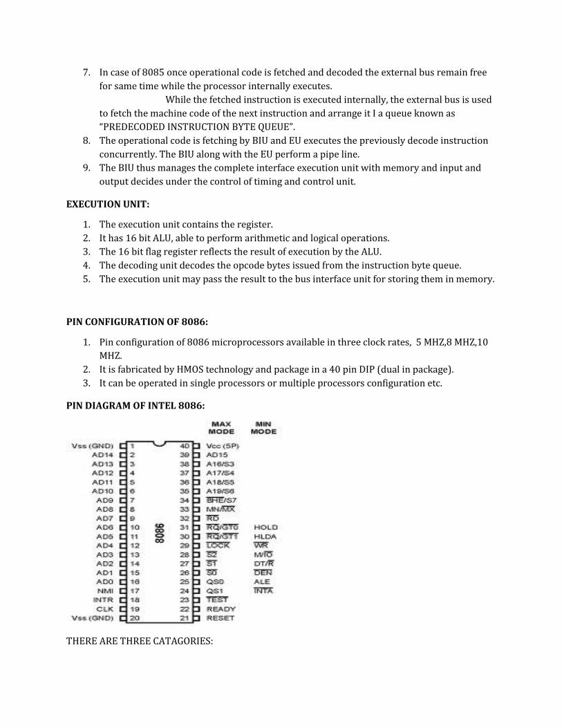
PIN DIAGRAM OF INTEL 8086:
THERE ARE THREE CATAGORIES:
1. Common pins
2. Pins required during minimum mode.
3. Pins required during maximum mode.
COMMON PINS IN 8086:
ADDRESS AND DATA BUS (AD0-AD15):
• Pin 2-16, 39(TYPES- INPUT /OUTPUT OPERATIONS).
FUNCTIONS:
These are the time multiplexed memory input , output address and data bus pins. The address part
(A0-A15) is transferred in T1 clock cycle and data are transferred in T2, T3, TW, T4 clock cycle. These
signals are stored by address latch enable (ALE) signals generated at a beginning of T1 states these
AD0- AD15 pins are traced in order to make AD0-AD15 lines receive the data signal.
ADDRESS AND STATUS LINES:-
• Pin number 35-38
• Type – output
• Function:-
These pins are called address/ status pin in T1 state a high on these pins specifies a memory
operation and low specific input / output operations the status information is available on
that line during T2, T3 and T4 clock cycles. The S5 pin is used to show the status interrupt
flag at the beginning of each clock cycle A16/S3 and A17/S4 are encoded as shown in table.
S4 S3 CHARACTERISTICS
0 0 EXTRA SEGMENT
0 1 STACK SEGMENT
1 0 CODE SEGMENT
1 1 DATA SEGMENT
BUS HIGH ENABLE/ STATUS:
• PIN NO.- 34
• TYPE- OUTPUT.
• FUNCTION
During T1 period (BHE)’ is low read , write and intercept acknowledgement operations ,
when a data byte is transferred on the data bus to form an odd address location or a 16 bit

transfer takes place from an even address on (D0-D15) data bus, the function of (BHE)’ is
shown in the table below.
(BHE)’ A0 OPERATION
0 0 16 BIT TRANSFER
0 1 UPPER BYTE TRANSER
1 0 LOWER BYTE TRANSFER
1 1 NONE
(RD)’ READ PIN: -
PIN NO.- 32
Type – output
Function:
This signal indicates that up is performing a memory or input output read operation.
READY:
PIN NO.- 22
TYPE- INPUT
FUNCTION:
The microprocessors sample , the ready signal at rising edge clock during T3 clock cycle, if the
signal is active high then microprocessors enter no wait states in its internal operation , otherwise
its enter wait state , in its internal operation.
INTR:
PIN NO.V- 18
TYPE- INPUT
FUNCTION:
This signal is sampled during last clock of each instruction to determine whether the
microprocessor should enter into an interrupt acknowledgement cycle.
(TEST)’:
PIN NO - 23
TYPE – INPUT
FUNCTION:
The signal is used in wait instruction before execution the instruction microprocessor check the
(TEST)’ pin status.
If TEST =1, then microprocessor will not enter into wait state , that is - execution will continue.
If TEST = 0, then the microprocessor will enter into wait state.
NMI(NON MARKABLE INTERRUPT):
PIN- 17
TYPE: - INPUT
FUNCTION:
This signal cannot be makeable internally by software. this is a edge triggered signal which cause a
type 2 interrupt when signal is active high interrupt service is vector to via an interrupt vector.
RESET:
PIN NO.- 21
TYPE- INPUT
FUNCTION:-
When this pin is high it immediate reset the microprocessor, When the pin status is high
immediately the segment count is FFFFH and so the base address at that moment is FFFF0H
3. REGISTER ORGANISATION:-
The INTEL 8086 contains the following register
(a) General purpose register
(b) Pointer and index register
(c) Segment register
(d) Instruction pointer
(e) Status Flags
(a) General Purpose register:-
(i) The AX, BX, CX and DX are the general purpose 16-bit register.
(ii) AX is used as 16-bit accumulator.
(iii) AX ->AH (For higher 8-bit)
� AL (For lower 8-bit)
BX-> Serve as base register for the computation of memory address.
CX-> Used as counter in case of multi-iteration .
DX-> used for memory addressing when the data are transferred between i/o port and memory
using certain i/o instruction.
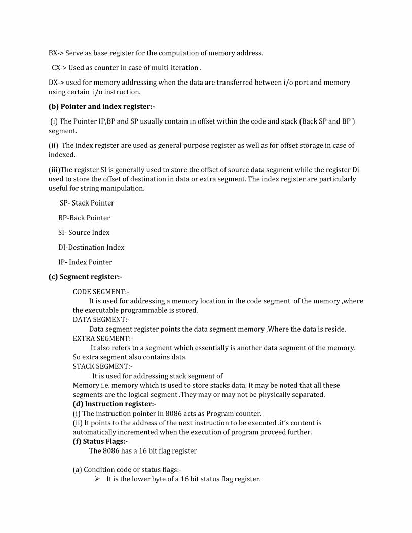
(b) Pointer and index register:-
(i) The Pointer IP,BP and SP usually contain in offset within the code and stack (Back SP and BP )
segment.
(ii) The index register are used as general purpose register as well as for offset storage in case of
indexed.
(iii)The register SI is generally used to store the offset of source data segment while the register Di
used to store the offset of destination in data or extra segment. The index register are particularly
useful for string manipulation.
SP- Stack Pointer
BP-Back Pointer
SI- Source Index
DI-Destination Index
IP- Index Pointer
(c) Segment register:-
CODE SEGMENT:-
It is used for addressing a memory location in the code segment of the memory ,where
the executable programmable is stored.
DATA SEGMENT:-
Data segment register points the data segment memory ,Where the data is reside.
EXTRA SEGMENT:-
It also refers to a segment which essentially is another data segment of the memory.
So extra segment also contains data.
STACK SEGMENT:-
It is used for addressing stack segment of
Memory i.e. memory which is used to store stacks data. It may be noted that all these
segments are the logical segment .They may or may not be physically separated.
(d) Instruction register:-
(i) The instruction pointer in 8086 acts as Program counter.
(ii) It points to the address of the next instruction to be executed .it’s content is
automatically incremented when the execution of program proceed further.
(f) Status Flags:-
The 8086 has a 16 bit flag register
(a) Condition code or status flags:-
� It is the lower byte of a 16 bit status flag register.
� It contains sign flag, zero flag, auxiliary carry flag, Parity flag and overflow flag.
(b) Machine cycle:-
� It is the higher byte of 16 bit status flag register.
� It contains directional flag, Trap flag, Interrupt flag etc.
(1) Carry Flag:-
The flag register is set to 1 when there is unsigned overflow. When there is no overflow this flag is
set 0.
(2) Parity Flag:-
The flag is set to be 1 when there is even no. of one bits in result and it 0 when there is odd
no. of one bits.
(3)Auxiliary Flag:-
Set to be 1 when there is an unsigned overflow for low nibble (4 bits).
(4)Zero Flag:-
Set to be 1 when result is zero, for non-zero results this flag is set to 0.
(5)Sign Flag:-
Set to 1 when result is negative, when result is positive it is set to 0.
(6) Trap Flag:-
It is set; the processor enters the single step execution mode or a trap interrupt generated
after execution of each instruction.
(7)Direction Flag:-
This is used string manipulation instruction D=0, then the string is processed beginning
from lower address to the higher address.
D=1, then the string is processed beginning higher address to the lower address.
(8)Interrupt Flag:-
This flag is set, the mask able interrupt recognized by the CPU otherwise they are ignored.
(9)Overflow Flag:-
This flag is set, if an overflow occurs i.e. if the result signed operation is large enough to
accommodate in a destination register.
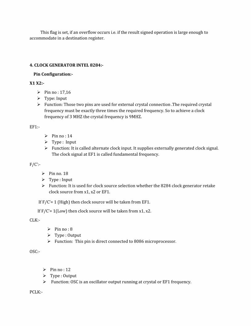
4. CLOCK GENERATOR INTEL 8284:-
Pin Configuration:-
X1 X2:-
� Pin no : 17,16
� Type: Input
� Function: Those two pins are used for external crystal connection .The required crystal
frequency must be exactly three times the required frequency. So to achieve a clock
frequency of 3 MHZ the crystal frequency is 9MHZ.
EF1:-
� Pin no : 14
� Type : Input
� Function: It is called alternate clock input. It supplies externally generated clock signal.
The clock signal at EF1 is called fundamental frequency.
F/C’:-
� Pin no. 18
� Type : Input
� Function: It is used for clock source selection whether the 8284 clock generator retake
clock source from x1, x2 or EF1.
If F/C’= 1 (High) then clock source will be taken from EF1.
If F/C’= 1(Low) then clock source will be taken from x1, x2.
CLK:-
� Pin no : 8
� Type : Output
� Function: This pin is direct connected to 8086 microprocessor.
OSC:-
� Pin no : 12
� Type : Output
� Function: OSC is an oscillator output running at crystal or EF1 frequency.
PCLK:-

� Pin no : 2
� Type : Output
� Function: It is TTL clock signal output for circuit. The frequency of PCLK is half of clock
frequency i.e. 50% duty cycle.
CSYNC:-
� Pin no : 1
� Type: Output
� Function: It is used to synchronise the clock signal in a multiprocessor environment.
When CSYNC=1 the 8284 clock generator /driver is stopped.
When CSYNC=0 the clock output restart.
RES’:-
� Pin no : 11
� Type : Input
� Function: This pin is called reset logic input. This signal is given by an external device
to reset the 8086 microprocessor.
RESET:-
� Pin no : 10
� Type : Output
�
� Function: For a smooth operation the reset signal must be synchronised with clock.
RDY1, RDY2:-
� Pin no : 4,6
� Type : Input
� Function: This pin enables the bus cycle extension by in sorting wait state between T3
and T4 clock period.
READY:-
� Pin no : 5
� Type : Output
� Function: These pins are called wait state ready inputs. It is used by slower devices
to request for extension of bus cycle.
AEN1’, AEN2’:-
� Pin no : 3,7
� Type : Input

� Function: To support multi bus configuration two ready inputs RDY1, RDY2 are
active. The AEN1’ and AEN2’ are there to provide arbitrate bus priorities when both
RDY1 and RDY2 are active.
ASYNC’:-
� Pin no : 15
� Type: This pin is called ready synchronization selection input. It selects either one or
two stage of synchronization for RDY1 and RDY2.
VCC:-
� Pin no : 18
� Function: connect to power source +5V.
GND:-
� Pin no : 9
� Type: Connect to ground.
5. BIDIRCTONAL BUS TRANSRECIVER INTEL 8286/8287:-
� The 8286 and 8287 are bidirectional system bus buffers or drivers. When the T pin is low,
the data at pins B. Will be sent to output through pin A.
When T is high the data at a pin will be send to output through pin B. OE’ is
low during data transfer operation.
� The function of these two chips is same. The only difference lies with their drive capacity.
� The 8286 transfers the data without altering them where as 8287 alter the data while
sending.
� Generally the 8286 is used. The T pin 8286 is connected to DT/R’ pin of 8086
microprocessor and OE’ pin is connected to DEN’ pin of 8086 microprocessor.
6. BUS CONTROLLER INTEL 8086:-
Pin description:
S0’, S1’, S2’:-
� Pin no : 3,19,18
� Type: Input
� Function: These three signals are called bus cycle status signals.
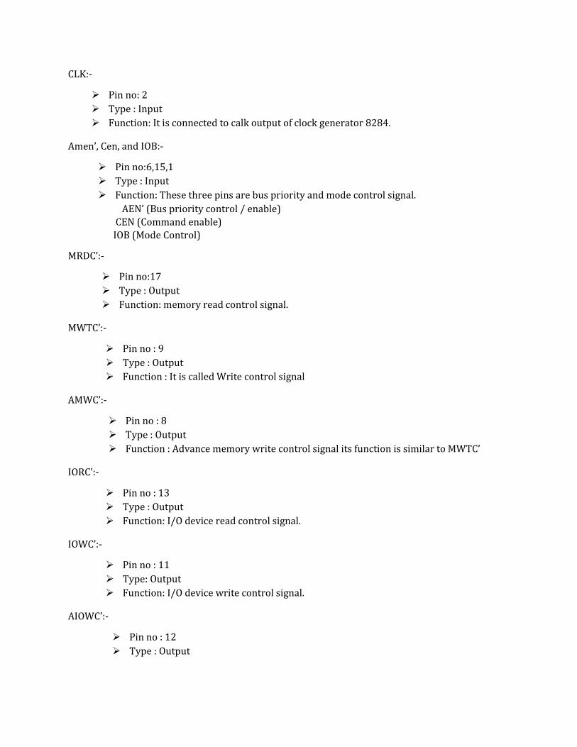
CLK:-
� Pin no: 2
� Type : Input
� Function: It is connected to calk output of clock generator 8284.
Amen’, Cen, and IOB:-
� Pin no:6,15,1
� Type : Input
� Function: These three pins are bus priority and mode control signal.
AEN’ (Bus priority control / enable)
CEN (Command enable)
IOB (Mode Control)
MRDC’:-
� Pin no:17
� Type : Output
� Function: memory read control signal.
MWTC’:-
� Pin no : 9
� Type : Output
� Function : It is called Write control signal
AMWC’:-
� Pin no : 8
� Type : Output
� Function : Advance memory write control signal its function is similar to MWTC’
IORC’:-
� Pin no : 13
� Type : Output
� Function: I/O device read control signal.
IOWC’:-
� Pin no : 11
� Type: Output
� Function: I/O device write control signal.
AIOWC’:-
� Pin no : 12
� Type : Output

� Function: This pin is called advance I/O device write control signal. It activate just
before the IOWC’.
INTA’:-
� Pin no : 14
� Type : Output
� Function: This pin is called interrupt acknowledgment. This signal is given by the
microprocessor to interrupting programme.
MCE/PDEN’:-
� Pin no : 7
� Type : Output
� Function: This pin is called cascade /Peripheral data enable. It is used with 8259
programmable interrupt controller.
ALE:-
� Pin no : 5
� Type : Output
� Function: Address latch enable pin.
DT/R’:-
� Pin no: 4
� Type : Output
� Function : Data direction control signal
DEN:-
� Pin no : 16
� Type : Output
� Function : data buffer control signal
GND:-
� Pin no : 10
� The 8288 Works In 2 mode like
� I/O bus mode
� System bus mode
7. TIMING DIGRAM OF (MEMORY /IO) READ:-
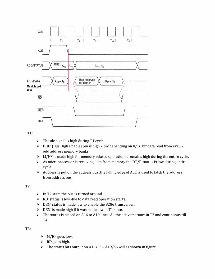
T1:
� The ale signal is high during T1 cycle.
� BHE’ (Bus High Enable) pin is high /low depending on 8/16 bit data read from even /
odd address memory banks.
� M/IO’ is made high for memory related operation it remains high during the entire cycle.
� As microprocessor is receiving data from memory the DT/R’ status is low during entire
cycle.
� Address is put on the address bus .the falling edge of ALE is used to latch the address
from address bus.
T2:
� In T2 state the bus is turned around.
� RD’ status is low due to data read operation starts.
� DEN’ status is made low to enable the 8286 transceiver.
� DEN’ is made high if it was made low in T1 state.
� The status is placed on A16 to A19 lines. All the activates start in T2 and continuous till
T4.
T3:
� M/IO’ goes low.
� RD’ goes high.
� The status bits output on A16/S3 – A19/S6 will as shown in figure.
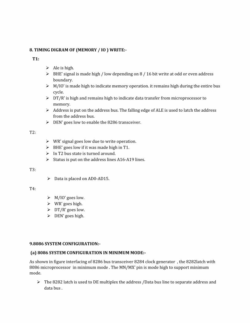
8. TIMING DIGRAM OF (MEMORY / IO ) WRITE:-
T1:
� Ale is high.
� BHE’ signal is made high / low depending on 8 / 16 bit write at odd or even address
boundary.
� M/IO’ is made high to indicate memory operation. it remains high during the entire bus
cycle.
� DT/R’ is high and remains high to indicate data transfer from microprocessor to
memory.
� Address is put on the address bus. The falling edge of ALE is used to latch the address
from the address bus.
� DEN’ goes low to enable the 8286 transceiver.
T2:
� WR’ signal goes low due to write operation.
� BHE’ goes low if it was made high in T1.
� In T2 bus state is turned around.
� Status is put on the address lines A16-A19 lines.
T3:
� Data is placed on AD0-AD15.
T4:
� M/IO’ goes low.
� WR’ goes high.
� DT/R’ goes low.
� DEN’ goes high.
9.8086 SYSTEM CONFIGURATION:-
(a) 8086 SYSTEM CONFIGURATION IN MINIMUM MODE:-
As shown in figure interfacing of 8286 bus transceiver 8284 clock generator , the 8282latch with
8086 microprocessor in minimum mode . The MN/MX’ pin is mode high to support minimum
mode.
� The 8282 latch is used to DE multiplex the address /Data bus line to separate address and
data bus .
� The ALE (Address Latch Enable) Signal is used to latch the address from address and data
lines.
� The 8284 clock generator is used to provide the CLK, READY, signals to the 8086
microprocessor.
� The 8284 generates the ready signal in synchronization with clock based on input at RDY1
pin. The RDY2 pin is connected in this configuration.
� The reset the 8086 microprocessor the reset pin remain high for 50ms.
� The data bus is bidirectional in nature. To create a separate data bus from address/data bus
two Intel 8286 bidirectional bus Transceiver is used.
� DT/R’ and DEN’ signal output of8086 microprocessor or are connected to 8086 as T and OE’
respectively.
(b) 8086 SYSTEM CONFIGURATION IN MAXIMUM MODE:-
As shown in figure the interfacing of 8286 bus transceiver , 8284 clock generator , 8282 latch with
8086 microprocessor in this case the MN/MX’ is made low to support the maximum mode
operation.
� The ALE ,DT/R’ and DEN’ signal are generated by 8288 bus controller.
� The IOB pin is grounded .it indicates that the 8288 is operating in system bus in which all
the signals are active.
� S2’,S1’,S0’ status signal of 8086 microprocessor are input to the 8288 which decodes
them and generates INTA’ , MRDC’ ,IORC’ , IOWC’ , ANWC’, and AIOWC, signals .These
signal are used for interfacing the 8086 microprocessor to memory and I/O device.
�
10.INTERRUPT:-
An interrupt is an external event which informs the CPU that a device needs service.
Normally Program can be interrupt by three ways
(a)By External device
(b)By a special instruction In the program
(c)By the occurrence of some condition.
HARDWARE INTERRUPT:-
An interrupt caused by an external signal is referred as a hardware interrupt.
SOFTWARE INTERRUPT:-
Conditional interrupts or interrupts caused by special instructions are called software interrupt.
(i) TYPE-0 INTERRUPT:-
� The divided by zero interrupt (type-0) automatically interrupt the 8086 when a divide
error occurs.
� The interrupt will occur if the quotient resulting from a division instruction or an IDIV
(Integer Division) instruction is too large to fit in the destination register.
(ii) TYPE-1 INTERRUPT:-
The single step interrupt will be enabled only if trap flag (TF) bit is set (=1).
� The TF bit can be SET/RESET by software.
� Single step control is used for debugging in assembly language in executing a sequence
of instruction.
� In this mode the processor executes one instruction and then stops.
� TRAP flag cannot be set directly .This is done by pushing on the stack ,changes are made
and then they are popped.
(iii) TYPE-2 INTERRUPT:-
� The non maskable interrupt is initialized through the 8086 NMI pin.
� This is used for vital system function such as power failures or external emergency
shutdown procedures.
� The NMI is edge triggered on a low to high transition .The activation of this pin causes a
type-2 interrupt.
� NMI has higher priority than the maskable interrupt request pin (INTRA)
(iv)TYPE-3 INTERRUPT:-
Type-3 interrupt or break point is a very special single byte software interrupt.
� The type-3 interrupt is produced by execution of the unit INT-3 instruction.
� The main use of the type-3 interrupt is to implement a break point function in a system or
used debugging software.
� In type-3 interrupt the system executes the instruction up to the break point and then
goes to the breakpoint procedure unlike the single step feature, which stop executing
about each instructions.
(v)TYPE-4 INTERRUPT:-
� The interrupt on overflow is a type -4 interrupt and occurs when the flag is set and
INTO instruction executed.
� The 8086 of will be set if the signed result or arithmetic operation on two signed
number is too large to represented in the destination result or memory location.
11. DMA (DIRECT MEMORY ACESS):-
In DMA the external logic circuit is allowed to access the memory directly and
perform read/write operation.
DMA In a minimum mode (MN/MX’):-
� The direct memory access in minimum mode is facilitated by HOLD and HLDA signals.
� When the external devices wants access the memory directly it request through a high
signal at HOLD pin.
� The 8086 microprocessor samples the HOLD signal at low high transition of clock.
� The 8086 microprocessor acknowledge the holds request by making the HLDA (HOLD
Acknowledgement) high at the end of current bus cycle.
� The external device accesses the memory and after completion of task it withdraw the
HOLD request by making the signal at HOLD pin low.
� The 8086 microprocessor check the HOLD pin at every low to high transition of clock
.After detecting the low signal at HOLD it will make the signal at HLDA low.
DMA In maximum mode (MN/MX’=0):-
� In maximum mode two signal RQ’/GT0’ and RQ1’/GT1’ are used for direct memory
access operation.
� The DMA request and DMA acknowledgment signal are received on same line.
� Thus RQ’/GT0’ and RQ1’/GT1’ are two channels for DMA by which two separate
external devices can access memory directly.
� The external device make a request for DMA by sending a low pulse at RQ’/GT’ ,The
8086 microprocessor samples the RQ’/GT’ signal at low to high transition of clock
period.
� The 8086 microprocessor acknowledgement the DMA request at the end of current bus
cycle by sending a low pulse on the same RQ’/GT’ pin .The address/data and control
signal float at the same time.
� After competition of memory operation the external devices informs the 8086
microprocessor by sending a low pulse on the RQ”/GT’ pin .The 8086 microprocessor
by sending a low on this pin and low –to-high transition of clock regains the control of
lines.
(12)HLT AND WAIT STATE:-
On the execution of HLT (Halt) instruction of 8086 ,CPU suspends its instruction execution and
enters into an idle state .It waits for either an external hardware interrupt or treat or a reset pin
(interrupt).When any one of these occurs ,CPU starts executing again.
When the wait instruction is executed by 8086 .it internally checks the logic
level existing at its TEST’ input .If TEST’ is at logic 1 state ,then CPU goes into an idle state .When
TEST’ input assume a zero state execution resume from the next sequential instruction in the
program.
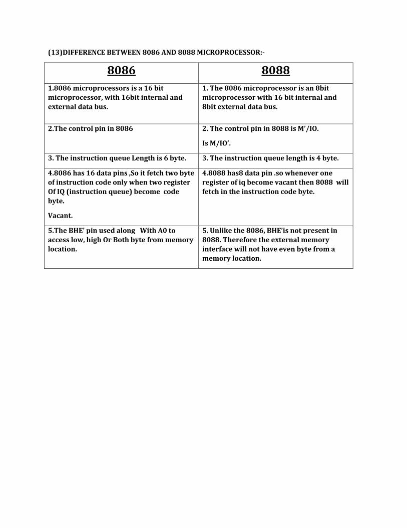
(13)DIFFERENCE BETWEEN 8086 AND 8088 MICROPROCESSOR:-
8086 8088
1.8086 microprocessors is a 16 bit
microprocessor, with 16bit internal and
external data bus.
1. The 8086 microprocessor is an 8bit
microprocessor with 16 bit internal and
8bit external data bus.
2.The control pin in 8086
2. The control pin in 8088 is M’/IO.
Is M/IO’.
3. The instruction queue Length is 6 byte. 3. The instruction queue length is 4 byte.
4.8086 has 16 data pins ,So it fetch two byte
of instruction code only when two register
Of IQ (instruction queue) become code
byte.
Vacant.
4.8088 has8 data pin .so whenever one
register of iq become vacant then 8088 will
fetch in the instruction code byte.
5.The BHE’ pin used along With A0 to
access low, high Or Both byte from memory
location.
5. Unlike the 8086, BHE’is not present in
8088. Therefore the external memory
interface will not have even byte from a
memory location.
MODULE 3
Instruction Set of 8086 The 8086 instructions are categorized into the following main types. i. Data Copy / Transfer Instructions ii. Arithmetic and Logical Instructions iii. Branch Instructions iv. Loop Instructions v. Machine Control Instructions vi. Flag Manipulation Instructions vii. Shift and Rotate Instructions viii. String Instructions Data Copy / Transfer Instructions : MOV : This instruction copies a word or a byte of data from some source to a destination. The destination can be a register or a memory location. The source can be a register, a memory location, or an immediate number. MOV AX,BX MOV AX,5000H MOV AX,[SI] MOV AX,[2000H] MOV AX,50H[BX] MOV [734AH],BX MOV DS,CX MOV CL,[357AH] Direct loading of the segment registers with immediate data is not permitted. 3 PUSH : Push to Stack This instruction pushes the contents of the specified register/memory location on to the stack. The stack pointer is decremented by 2, after each execution of the instruction. E.g. PUSH AX • PUSH DS • PUSH [5000H] Fig. 2 Push Data to stack memory POP : Pop from Sack This instruction when executed, loads the specified register/memory location with the contents of the memory location of which the address is formed using the current stack segment and stack pointer. The stack pointer is incremented by 2 Eg. POP AX POP DS POP [5000H] Fig 3 Popping Register Content from Stack Memory XCHG : Exchange byte or word This instruction exchange the contents of the specified source and destination operands Eg. XCHG [5000H], AX
XCHG BX, AX 4 XLAT : Translate byte using look-up table Eg. LEA BX, TABLE1 MOV AL, 04H XLAT Simple input and output port transfer Instructions: IN: Copy a byte or word from specified port to accumulator. Eg. IN AL,03H IN AX,DX OUT: Copy a byte or word from accumulator specified port. Eg. OUT 03H, AL OUT DX, AX LEA : Load effective address of operand in specified register. [reg] offset portion of address in DS Eg. LEA reg, offset LDS: Load DS register and other specified register from memory. [reg] [mem] [DS] [mem + 2] Eg. LDS reg, mem LES: Load ES register and other specified register from memory. [reg] [mem] [ES] [mem + 2] Eg. LES reg, mem Flag transfer instructions: LAHF: Load (copy to) AH with the low byte the flag register. [AH] [ Flags low byte] Eg. LAHF 5 SAHF: Store (copy) AH register to low byte of flag register. [Flags low byte] [AH] Eg. SAHF PUSHF: Copy flag register to top of stack. [SP] [SP] – 2 [[SP]] [Flags] Eg. PUSHF POPF : Copy word at top of stack to flag register. [Flags] [[SP]] [SP] [SP] + 2 Arithmetic Instructions: The 8086 provides many arithmetic operations: addition, subtraction, negation,

multiplication and comparing two values. ADD : The add instruction adds the contents of the source operand to the destination operand. Eg. ADD AX, 0100H ADD AX, BX ADD AX, [SI] ADD AX, [5000H] ADD [5000H], 0100H ADD 0100H ADC : Add with Carry This instruction performs the same operation as ADD instruction, but adds the carry flag to the result. Eg. ADC 0100H ADC AX, BX ADC AX, [SI] ADC AX, [5000] ADC [5000], 0100H 6 SUB : Subtract The subtract instruction subtracts the source operand from the destination operand and the result is left in the destination operand. Eg. SUB AX, 0100H SUB AX, BX SUB AX, [5000H] SUB [5000H], 0100H SBB : Subtract with Borrow The subtract with borrow instruction subtracts the source operand and the borrow flag (CF) which may reflect the result of the previous calculations, from the destination operand Eg. SBB AX, 0100H SBB AX, BX SBB AX, [5000H] SBB [5000H], 0100H INC : Increment This instruction increases the contents of the specified Register or memory location by 1. Immediate data cannot be operand of this instruction. Eg. INC AX INC [BX] INC [5000H] DEC : Decrement The decrement instruction subtracts 1 from the contents of the specified register or memory location. Eg. DEC AX DEC [5000H] NEG : Negate The negate instruction forms 2’s complement of the specified destination in the instruction. The destination can be a register or a memory location. This instruction can be implemented by inverting each bit and adding 1 to it. Eg. NEG AL AL = 0011 0101 35H Replace number in AL with its 2’s complement
AL = 1100 1011 = CBH CMP : Compare This instruction compares the source operand, which may be a register or an immediate data or a memory location, with a destination operand that may be a 7 register or a memory location Eg. CMP BX, 0100H CMP AX, 0100H CMP [5000H], 0100H CMP BX, [SI] CMP BX, CX MUL :Unsigned Multiplication Byte or Word This instruction multiplies an unsigned byte or word by the contents of AL. Eg. MUL BH ; (AX) (AL) x (BH) MUL CX ; (DX)(AX) (AX) x (CX) MUL WORD PTR [SI] ; (DX)(AX) (AX) x ([SI]) IMUL :Signed Multiplication This instruction multiplies a signed byte in source operand by a signed byte in AL or a signed word in source operand by a signed word in AX. Eg. IMUL BH IMUL CX IMUL [SI] CBW : Convert Signed Byte to Word This instruction copies the sign of a byte in AL to all the bits in AH. AH is then said to be sign extension of AL. Eg. CBW AX= 0000 0000 1001 1000 Convert signed byte in AL signed word in AX. Result in AX = 1111 1111 1001 1000 CWD : Convert Signed Word to Double Word This instruction copies the sign of a byte in AL to all the bits in AH. AH is then said to be sign extension of AL. Eg. CWD Convert signed word in AX to signed double word in DX : AX DX= 1111 1111 1111 1111 Result in AX = 1111 0000 1100 0001 DIV : Unsigned division This instruction is used to divide an unsigned word by a byte or to divide an unsigned double word by a word. Eg. DIV CL ; Word in AX / byte in CL ; Quotient in AL, remainder in AH DIV CX ; Double word in DX and AX / word ; in CX, and Quotient in AX, ; remainder in DX 8 AAA : ASCII Adjust After Addition The AAA instruction is executed aftr an ADD instruction that adds two ASCII coded operand to give a byte of result in AL. The AAA instruction converts the resulting contents of Al to a unpacked decimal digits. Eg. ADD CL, DL ; [CL] = 32H = ASCII for 2 ; [DL] = 35H = ASCII for 5 ; Result [CL] = 67H
MOV AL, CL ; Move ASCII result into AL since ; AAA adjust only [AL] AAA ; [AL]=07, unpacked BCD for 7 AAS : ASCII Adjust AL after Subtraction This instruction corrects the result in AL register after subtracting two unpacked ASCII operands. The result is in unpacked decimal format. The procedure is similar to AAA instruction except for the subtraction of 06 from AL. AAM : ASCII Adjust after Multiplication This instruction, after execution, converts the product available In AL into unpacked BCD format. Eg. MOV AL, 04 ; AL = 04 MOV BL ,09 ; BL = 09 MUL BL ; AX = AL*BL ; AX=24H AAM ; AH = 03, AL=06 AAD : ASCII Adjust before Division This instruction converts two unpacked BCD digits in AH and AL to the equivalent binary number in AL. This adjustment must be made before dividing the two unpacked BCD digits in AX by an unpacked BCD byte. In the instruction sequence, this instruction appears Before DIV instruction. Eg. AX 05 08 AAD result in AL 00 3A 58D = 3A H in AL The result of AAD execution will give the hexadecimal number 3A in AL and 00 in AH. Where 3A is the hexadecimal Equivalent of 58 (decimal). DAA : Decimal Adjust Accumulator This instruction is used to convert the result of the addition of two packed BCD numbers to a valid BCD number. The result has to be only in AL. Eg. AL = 53 CL = 29 ADD AL, CL ; AL (AL) + (CL) ; AL 53 + 29 ; AL 7C DAA ; AL 7C + 06 (as C>9) ; AL 82 9 DAS : Decimal Adjust after Subtraction This instruction converts the result of the subtraction of two packed BCD numbers to a valid BCD number. The subtraction has to be in AL only. Eg. AL = 75, BH = 46 SUB AL, BH ; AL 2 F = (AL) - (BH) ; AF = 1 DAS ; AL 2 9 (as F>9, F - 6 = 9) Logical Instructions AND : Logical AND This instruction bit by bit ANDs the source operand that may be an immediate register or a memory location to the destination operand that may a register or a memory location. The result is stored in the destination operand. Eg. AND AX, 0008H AND AX, BX OR : Logical OR This instruction bit by bit ORs the source operand that may be an immediate , register or a memory location to the destination operand that may a register or a memory location. The result is stored in the destination operand.
Eg. OR AX, 0008H OR AX, BX NOT : Logical Invert This instruction complements the contents of an operand register or a memory location, bit by bit. Eg. NOT AX NOT [5000H] XOR : Logical Exclusive OR This instruction bit by bit XORs the source operand that may be an immediate , register or a memory location to the destination operand that may a register or a memory location. The result is stored in the destination operand. Eg. XOR AX, 0098H XOR AX, BX TEST : Logical Compare Instruction The TEST instruction performs a bit by bit logical AND operation on the two operands. The result of this ANDing operation is not available for further use, but flags are affected. Eg. TEST AX, BX TEST [0500], 06H 10 SAL/SHL : SAL / SHL destination, count. SAL and SHL are two mnemonics for the same instruction. This instruction shifts each bit in the specified destination to the left and 0 is stored at LSB position. The MSB is shifted into the carry flag. The destination can be a byte or a word. It can be in a register or in a memory location. The number of shifts is indicated by count. Eg. SAL CX, 1 SAL AX, CL SHR : SHR destination, count This instruction shifts each bit in the specified destination to the right and 0 is stored at MSB position. The LSB is shifted into the carry flag. The destination can be a byte or a word. It can be a register or in a memory location. The number of shifts is indicated by count. Eg. SHR CX, 1 MOV CL, 05H SHR AX, CL SAR : SAR destination, count This instruction shifts each bit in the specified destination some number of bit positions to the right. As a bit is shifted out of the MSB position, a copy of the old MSB is put in the MSB position. The LSB will be shifted into CF. Eg. SAR BL, 1 MOV CL, 04H SAR DX, CL ROL Instruction : ROL destination, count This instruction rotates all bits in a specified byte or word to the left some number of bit positions. MSB is placed as a new LSB and a new CF. Eg. ROL CX, 1 MOV CL, 03H ROL BL, CL ROR Instruction : ROR destination, count
This instruction rotates all bits in a specified byte or word to the right some number of bit positions. LSB is placed as a new MSB and a new CF. Eg. ROR CX, 1 MOV CL, 03H ROR BL, CL 11 RCL Instruction : RCL destination, count This instruction rotates all bits in a specified byte or word some number of bit positions to the left along with the carry flag. MSB is placed as a new carry and previous carry is place as new LSB. Eg. RCL CX, 1 MOV CL, 04H RCL AL, CL RCR Instruction : RCR destination, count This instruction rotates all bits in a specified byte or word some number of bit positions to the right along with the carry flag. LSB is placed as a new carry and previous carry is place as new MSB. Eg. RCR CX, 1 MOV CL, 04H RCR AL, CL ROR Instruction : ROR destination, count This instruction rotates all bits in a specified byte or word to the right some number of bit positions. LSB is placed as a new MSB and a new CF. Eg. ROR CX, 1 MOV CL, 03H ROR BL, CL RCL Instruction : RCL destination, count This instruction rotates all bits in a specified byte or word some number of bit positions to the left along with the carry flag. MSB is placed as a new carry and previous carry is place as new LSB. Eg. RCL CX, 1 MOV CL, 04H RCL AL, CL RCR Instruction : RCR destination, count This instruction rotates all bits in a specified byte or word some number of bit positions to the right along with the carry flag. LSB is placed as a new carry and previous carry is place as new MSB. Eg. RCR CX, 1 MOV CL, 04H RCR AL, CL 12 Branch Instructions : Branch Instructions transfers the flow of execution of the program to a new address specified in the instruction directly or indirectly. When this type of instruction is executed, the CS and IP registers get loaded with new values of CS and IP corresponding to the location to be transferred. The Branch Instructions are classified into two types i. Unconditional Branch Instructions. ii. Conditional Branch Instructions. Unconditional Branch Instructions : In Unconditional control transfer instructions, the execution control is transferred

to the specified location independent of any status or condition. The CS and IP are unconditionally modified to the new CS and IP. CALL : Unconditional Call This instruction is used to call a Subroutine (Procedure) from a main program. Address of procedure may be specified directly or indirectly. There are two types of procedure depending upon whether it is available in the same segment or in another segment. i. Near CALL i.e., ±32K displacement. ii. For CALL i.e., anywhere outside the segment. On execution this instruction stores the incremented IP & CS onto the stack and loads the CS & IP registers with segment and offset addresses of the procedure to be called. RET: Return from the Procedure. At the end of the procedure, the RET instruction must be executed. When it is executed, the previously stored content of IP and CS along with Flags are retrieved into the CS, IP and Flag registers from the stack and execution of the main program continues further. INT N: Interrupt Type N. In the interrupt structure of 8086, 256 interrupts are defined corresponding to the types from 00H to FFH. When INT N instruction is executed, the type byte N is multiplied by 4 and the contents of IP and CS of the interrupt service routine will be taken from memory block in 0000 segment. 13 INTO: Interrupt on Overflow This instruction is executed, when the overflow flag OF is set. This is equivalent to a Type 4 Interrupt instruction. JMP: Unconditional Jump This instruction unconditionally transfers the control of execution to the specified address using an 8-bit or 16-bit displacement. No Flags are affected by this instruction. IRET: Return from ISR When it is executed, the values of IP, CS and Flags are retrieved from the stack to continue the execution of the main program. LOOP : LOOP Unconditionally This instruction executes the part of the program from the Label or address specified in the instruction upto the LOOP instruction CX number of times. At each iteration, CX is decremented automatically and JUMP IF NOT ZERO structure. Example: MOV CX, 0004H MOV BX, 7526H Label 1 MOV AX, CODE OR BX, AX LOOP Label 1 Conditional Branch Instructions When this instruction is executed, execution control is transferred to the address specified relatively in the instruction, provided the condition implicit in the Opcode is satisfied. Otherwise execution continues sequentially. JZ/JE Label Transfer execution control to address ‘Label’, if ZF=1. JNZ/JNE Label Transfer execution control to address ‘Label’, if ZF=0 JS Label Transfer execution control to address ‘Label’, if SF=1.
JNS Label Transfer execution control to address ‘Label’, if SF=0. JO Label Transfer execution control to address ‘Label’, if OF=1. 14 JNO Label Transfer execution control to address ‘Label’, if OF=0. JNP Label Transfer execution control to address ‘Label’, if PF=0. JP Label Transfer execution control to address ‘Label’, if PF=1. JB Label Transfer execution control to address ‘Label’, if CF=1. JNB Label Transfer execution control to address ‘Label’, if CF=0. JCXZ Label Transfer execution control to address ‘Label’, if CX=0 Conditional LOOP Instructions. LOOPZ / LOOPE Label Loop through a sequence of instructions from label while ZF=1 and CX=0. LOOPNZ / LOOPENE Label Loop through a sequence of instructions from label while ZF=1 and CX=0. String Manipulation Instructions A series of data byte or word available in memory at consecutive locations, to be referred as Byte String or Word String. A String of characters may be located in consecutive memory locations, where each character may be represented by its ASCII equivalent. The 8086 supports a set of more powerful instructions for string manipulations for referring to a string, two parameters are required. I. Starting and End Address of the String. II. Length of the String. The length of the string is usually stored as count in the CX register.The incrementing or decrementing of the pointer, in string instructions, depends upon the Direction Flag (DF) Status. If it is a Byte string operation, the index registers are updated 15 by one. On the other hand, if it is a word string operation, the index registers are updated by two. REP : Repeat Instruction Prefix This instruction is used as a prefix to other instructions, the instruction to which the REP prefix is provided, is executed repeatedly until the CX register becomes zero (at each iteration CX is automatically decremented by one). i. REPE / REPZ - repeat operation while equal / zero. ii. REPNE / REPNZ - repeat operation while not equal / not zero. These are used for CMPS, SCAS instructions only, as instruction prefixes. MOVSB / MOVSW :Move String Byte or String Word Suppose a string of bytes stored in a set of consecutive memory locations is to be moved to another set of destination locations.The starting byte of source string is located in the memory location whose address may be computed using SI (Source Index) and DS (Data Segment) contents. The starting address of the destination locations where this string has to be relocated is given by DI (Destination Index) and ES (Extra Segment) contents.
CMPS : Compare String Byte or String Word The CMPS instruction can be used to compare two strings of byte or words. The length of the string must be stored in the register CX. If both the byte or word strings are equal, zero Flag is set. The REP instruction Prefix is used to repeat the operation till CX (counter) becomes zero or the condition specified by the REP Prefix is False. SCAN : Scan String Byte or String Word This instruction scans a string of bytes or words for an operand byte or word specified in the register AL or AX. The String is pointed to by ES:DI register pair. The length of the string s stored in CX. The DF controls the mode for scanning of the string. Whenever a match to the specified operand, is found in the string, execution stops and the zero Flag is set. If no match is found, the zero flag is reset. LODS : Load String Byte or String Word The LODS instruction loads the AL / AX register by the content of a string pointed to by DS : SI register pair. The SI is modified automatically depending upon DF, If it is a byte transfer (LODSB), the SI is modified by one and if it is a word transfer (LODSW), the SI is modified by two. No other Flags are affected by this instruction. 16 STOS : Store String Byte or String Word The STOS instruction Stores the AL / AX register contents to a location in the string pointer by ES : DI register pair. The DI is modified accordingly, No Flags are affected by this instruction. The direction Flag controls the String instruction execution, The source index SI and Destination Index DI are modified after each iteration automatically. If DF=1, then the execution follows autodecrement mode, SI and DI are decremented automatically after each iteration. If DF=0, then the execution follows autoincrement mode. In this mode, SI and DI are incremented automatically after each iteration. Flag Manipulation and a Processor Control Instructions These instructions control the functioning of the available hardware inside the processor chip. These instructions are categorized into two types: 1. Flag Manipulation instructions. Machine Control instructions. Flag Manipulation instructions The Flag manipulation instructions directly modify some of the Flags of 8086. i. CLC – Clear Carry Flag. ii. CMC – Complement Carry Flag. iii. STC – Set Carry Flag. iv. CLD – Clear Direction Flag. v. STD – Set Direction Flag. vi. CLI – Clear Interrupt Flag. vii. STI – Set Interrupt Flag. Machine Control instructions The Machine control instructions control the bus usage and execution i. WAIT – Wait for Test input pin to go low. ii. HLT – Halt the process. iii. NOP – No operation. iv. ESC – Escape to external device like NDP v. LOCK – Bus lock instruction prefix. 17 Addressing Modes Addressing modes of 8086
When 8086 executes an instruction, it performs the specified function on data. These data are called its operands and may be part of the instruction, reside in one of the internal registers of the microprocessor, stored at an address in memory or held at an I/O port, to access these different types of operands, the 8086 is provided with various addressing modes (Data Addressing Modes). Data Addressing Modes of 8086 The 8086 has 12 addressing modes. The various 8086 addressing modes can be classified into five groups. A. Addressing modes for accessing immediate and register data (register and immediate modes). B. Addressing modes for accessing data in memory (memory modes) C. Addressing modes for accessing I/O ports (I/O modes) D. Relative addressing mode E. Implied addressing mode 8086 ADDRESSING MODES A. Immediate addressing mode: In this mode, 8 or 16 bit data can be specified as part of the instruction. OP Code Immediate Operand Example 1 : MOV CL, 03 H Moves the 8 bit data 03 H into CL Example 2 : MOV DX, 0525 H Moves the 16 bit data 0525 H into DX In the above two examples, the source operand is in immediate mode and the destination operand is in register mode. A constant such as “VALUE” can be defined by the assembler EQUATE directive such as VALUE EQU 35H Example : MOV BH, VALUE Used to load 35 H into BH Register addressing mode : The operand to be accessed is specified as residing in an internal register of 8086. Fig. below shows internal registers, any one can be used as a source or destination operand, however only the data registers can be accessed as either a byte or word. 18 Register Operand sizes Byte (Reg 8) Word (Reg 16) Accumulator AL, AH Ax Base BL, BH Bx Count CL, CH Cx Data DL, DH Dx Stack pointer - SP Base pointer - BP Source index - SI Destination index - DI Code Segment - CS Data Segment - DS Stack Segment - SS Extra Segment - ES Example 1 : MOV DX (Destination Register) , CX (Source Register) Which moves 16 bit content of CS into DX. Example 2 : MOV CL, DL

Moves 8 bit contents of DL into CL MOV BX, CH is an illegal instruction. * The register sizes must be the same. B. Direct addressing mode : The instruction Opcode is followed by an affective address, this effective address is directly used as the 16 bit offset of the storage location of the operand from the location specified by the current value in the selected segment register. The default segment is always DS. The 20 bit physical address of the operand in memory is normally obtained as PA = DS : EA But by using a segment override prefix (SOP) in the instruction, any of the four segment registers can be referenced, PA = CS DS : Direct Address SS ES The Execution Unit (EU) has direct access to all registers and data for register and immediate operands. However the EU cannot directly access the memory operands. It must use the BIU, in order to access memory operands. 19 In the direct addressing mode, the 16 bit effective address (EA) is taken directly from the displacement field of the instruction. Example 1 :MOV CX, START If the 16 bit value assigned to the offset START by the programmer using an assembler pseudo instruction such as DW is 0040 and [DS] = 3050. Then BIU generates the 20 bit physical address 30540 H. The content of 30540 is moved to CL The content of 30541 is moved to CH Example 2 :MOV CH, START If [DS] = 3050 and START = 0040 8 bit content of memory location 30540 is moved to CH. Example 3 :MOV START, BX With [DS] = 3050, the value of START is 0040. Physical address : 30540 MOV instruction moves (BL) and (BH) to locations 30540 and 30541 respectively. Register indirect addressing mode : The EA is specified in either pointer (BX) register or an index (SI or DI) register. The 20 bit physical address is computed using DS and EA. Example : MOV [DI], BX register indirect If [DS] = 5004, [DI] = 0020, [Bx] = 2456 PA=50060. The content of BX(2456) is moved to memory locations 50060 H and 50061 H. CS PA = DS BX SS = SI ES DI Based addressing mode: CS PA = DS BX SS : or + displacement ES BP
when memory is accessed PA is computed from BX and DS when the stack is accessed PA is computed from BP and SS. Example : MOV AL, START [BX] or MOV AL, [START + BX] based mode EA : [START] + [BX] PA : [DS] + [EA] The 8 bit content of this memory location is moved to AL. 20 Indexed addressing mode: CS PA = DS SI SS : or + 8 or 16bit displacement ES DI Example : MOV BH, START [SI] PA : [SART] + [SI] + [DS] The content of this memory is moved into BH. Based Indexed addressing mode: CS PA = DS BX SI SS : or + or + 8 or 16bit displacement ES BP DI Example : MOV ALPHA [SI] [BX], CL If [BX] = 0200, ALPHA – 08, [SI] = 1000 H and [DS] = 3000 Physical address (PA) = 31208 8 bit content of CL is moved to 31208 memory address. String addressing mode: The string instructions automatically assume SI to point to the first byte or word of the source operand and DI to point to the first byte or word of the destination operand. The contents of SI and DI are automatically incremented (by clearing DF to 0 by CLD instruction) to point to the next byte or word. Example : MOV S BYTE If [DF] = 0, [DS] = 2000 H, [SI] = 0500, [ES] = 4000, [DI] = 0300 Source address : 20500, assume it contains 38 PA : [DS] + [SI] Destination address : [ES] + [DI] = 40300, assume it contains 45 After executing MOV S BYTE, [40300] = 38 [SI] = 0501 incremented [DI] = 0301 C. I/O mode (direct) : Port number is an 8 bit immediate operand. Example : OUT 05 H, AL Outputs [AL] to 8 bit port 05 H I/O mode (indirect): The port number is taken from DX. Example 1 : INAL, DX 21 OR
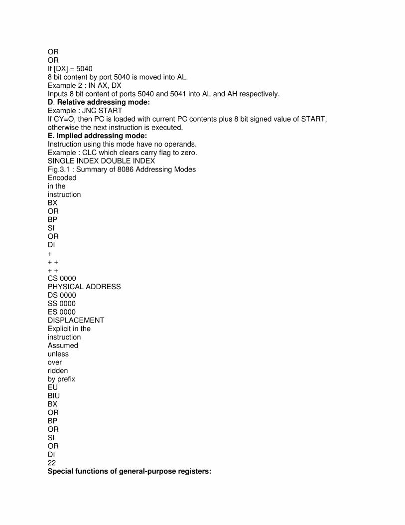
OR OR If [DX] = 5040 8 bit content by port 5040 is moved into AL. Example 2 : IN AX, DX Inputs 8 bit content of ports 5040 and 5041 into AL and AH respectively. D. Relative addressing mode: Example : JNC START If CY=O, then PC is loaded with current PC contents plus 8 bit signed value of START, otherwise the next instruction is executed. E. Implied addressing mode: Instruction using this mode have no operands. Example : CLC which clears carry flag to zero. SINGLE INDEX DOUBLE INDEX Fig.3.1 : Summary of 8086 Addressing Modes Encoded in the instruction BX OR BP SI OR DI + + + + + CS 0000 PHYSICAL ADDRESS DS 0000 SS 0000 ES 0000 DISPLACEMENT Explicit in the instruction Assumed unless over ridden by prefix EU BIU BX OR BP OR SI OR DI 22 Special functions of general-purpose registers:
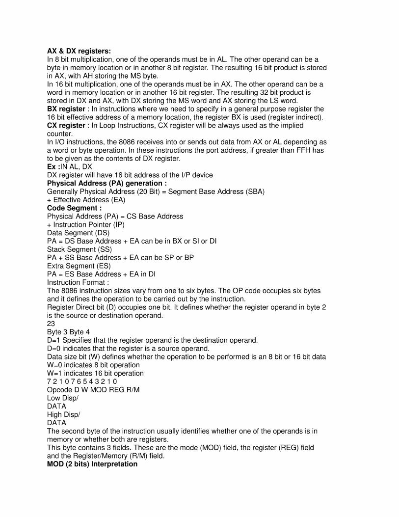
AX & DX registers: In 8 bit multiplication, one of the operands must be in AL. The other operand can be a byte in memory location or in another 8 bit register. The resulting 16 bit product is stored in AX, with AH storing the MS byte. In 16 bit multiplication, one of the operands must be in AX. The other operand can be a word in memory location or in another 16 bit register. The resulting 32 bit product is stored in DX and AX, with DX storing the MS word and AX storing the LS word. BX register : In instructions where we need to specify in a general purpose register the 16 bit effective address of a memory location, the register BX is used (register indirect). CX register : In Loop Instructions, CX register will be always used as the implied counter. In I/O instructions, the 8086 receives into or sends out data from AX or AL depending as a word or byte operation. In these instructions the port address, if greater than FFH has to be given as the contents of DX register. Ex :IN AL, DX DX register will have 16 bit address of the I/P device Physical Address (PA) generation : Generally Physical Address (20 Bit) = Segment Base Address (SBA) + Effective Address (EA) Code Segment : Physical Address (PA) = CS Base Address + Instruction Pointer (IP) Data Segment (DS) PA = DS Base Address + EA can be in BX or SI or DI Stack Segment (SS) PA + SS Base Address + EA can be SP or BP Extra Segment (ES) PA = ES Base Address + EA in DI Instruction Format : The 8086 instruction sizes vary from one to six bytes. The OP code occupies six bytes and it defines the operation to be carried out by the instruction. Register Direct bit (D) occupies one bit. It defines whether the register operand in byte 2 is the source or destination operand. 23 Byte 3 Byte 4 D=1 Specifies that the register operand is the destination operand. D=0 indicates that the register is a source operand. Data size bit (W) defines whether the operation to be performed is an 8 bit or 16 bit data W=0 indicates 8 bit operation W=1 indicates 16 bit operation 7 2 1 0 7 6 5 4 3 2 1 0 Opcode D W MOD REG R/M Low Disp/ DATA High Disp/ DATA The second byte of the instruction usually identifies whether one of the operands is in memory or whether both are registers. This byte contains 3 fields. These are the mode (MOD) field, the register (REG) field and the Register/Memory (R/M) field. MOD (2 bits) Interpretation
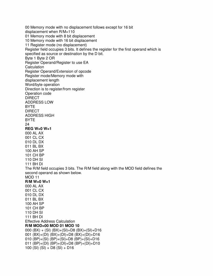
00 Memory mode with no displacement follows except for 16 bit displacement when R/M=110 01 Memory mode with 8 bit displacement 10 Memory mode with 16 bit displacement 11 Register mode (no displacement) Register field occupies 3 bits. It defines the register for the first operand which is specified as source or destination by the D bit. Byte 1 Byte 2 OR Register Operand/Register to use EA Calculation Register Operand/Extension of opcode Register mode/Memory mode with displacement length Word/byte operation Direction is to register/from register Operation code DIRECT ADDRESS LOW BYTE DIRECT ADDRESS HIGH BYTE 24 REG W=0 W=1 000 AL AX 001 CL CX 010 DL DX 011 BL BX 100 AH SP 101 CH BP 110 DH SI 111 BH DI The R/M field occupies 3 bits. The R/M field along with the MOD field defines the second operand as shown below. MOD 11 R/M W=0 W=1 000 AL AX 001 CL CX 010 DL DX 011 BL BX 100 AH SP 101 CH BP 110 DH SI 111 BH DI Effective Address Calculation R/M MOD=00 MOD 01 MOD 10 000 (BX) + (SI) (BX)+(SI)+D8 (BX)+(SI)+D16 001 (BX)+(DI) (BX)+(DI)+D8 (BX)+(DI)+D16 010 (BP)+(SI) (BP)+(SI)+D8 (BP)+(SI)+D16 011 (BP)+(DI) (BP)+(DI)+D8 (BP)+(DI)+D10 100 (SI) (SI) + D8 (SI) + D16

101 (DI) (DI) + D8 (DI) + D16 110 Direct address (BP) + D8 (BP) + D16 111 (BX) (BX) + D8 (BX) + D16 In the above, encoding of the R/M field depends on how the mode field is set. If MOD=11 (register to register mode), this R/M identifies the second register operand. MOD selects memory mode, then R/M indicates how the effective address of the memory operand is to be calculated. Bytes 3 through 6 of an instruction are optional fields that normally contain the displacement value of a memory operand and / or the actual value of an immediate constant operand. Example 1 : MOV CH, BL This instruction transfers 8 bit content of BL 25 Into CH The 6 bit Opcode for this instruction is 1000102 D bit indicates whether the register specified by the REG field of byte 2 is a source or destination operand. D=0 indicates BL is a source operand. W=0 byte operation In byte 2, since the second operand is a register MOD field is 11 The R/M field = 101 (CH) Register (REG) field = 011 (BL) Hence the machine code for MOV CH, BL is 10001000 11 011 101 Byte 1 Byte2 = 88DD16 Example 2 : SUB Bx, (DI) This instruction subtracts the 16 bit content of memory location addressed by DI and DS from Bx. The 6 bit Opcode for SUB is 001010 D=1 so that REG field of byte 2 is the destination operand. W=1 indicates 16 bit operation. MOD = 00 REG = 011 R/M = 101 The machine code is 0010 1011 0001 1101 2 B 1 D 2B1D16 Summary of all Addressing Modes Example 3 : Code for MOV 1234 (BP), DX Here we have specify DX using REG field, the D bit must be 0, indicating the DX is the source register. The REG field must be 010 to indicate DX register. The W bit must be 1 to indicate it is a word operation. 1234 [BP] is specified using MOD value of 10 and R/M value of 110 and a displacement of 1234H. The 4 byte code for this instruction would be 89 96 34 12H. MOD / R/M Memory Mode (EA Calculation) Register Mode 00 01 10 W=0 W=1 000 (BX)+(SI) (BX)+(SI)+d8 (BX)+(SI)+d16 AL AX 001 (BX) + (DI) (BX)+(DI)+d8 (BX)+(DI)+d16 CL CX 010 (BP)+(SI) (BP)+(SI)+d8 (BP)+(SI)+d16 DL DX 011 (BP)+(DI) (BP)+(DI)+d8 (BP)+(DI)+d16 BL BX 100 (SI) (SI) + d8 (SI) + d16 AH SP 101 (DI) (DI) + d8 (DI) + d16 CH BP 110 d16 (BP) + d8 (BP) + d16 DH SI
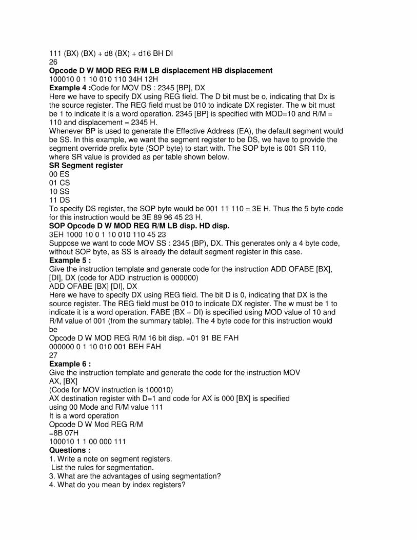
111 (BX) (BX) + d8 (BX) + d16 BH DI 26 Opcode D W MOD REG R/M LB displacement HB displacement 100010 0 1 10 010 110 34H 12H Example 4 :Code for MOV DS : 2345 [BP], DX Here we have to specify DX using REG field. The D bit must be o, indicating that Dx is the source register. The REG field must be 010 to indicate DX register. The w bit must be 1 to indicate it is a word operation. 2345 [BP] is specified with MOD=10 and R/M = 110 and displacement = 2345 H. Whenever BP is used to generate the Effective Address (EA), the default segment would be SS. In this example, we want the segment register to be DS, we have to provide the segment override prefix byte (SOP byte) to start with. The SOP byte is 001 SR 110, where SR value is provided as per table shown below. SR Segment register 00 ES 01 CS 10 SS 11 DS To specify DS register, the SOP byte would be 001 11 110 = 3E H. Thus the 5 byte code for this instruction would be 3E 89 96 45 23 H. SOP Opcode D W MOD REG R/M LB disp. HD disp. 3EH 1000 10 0 1 10 010 110 45 23 Suppose we want to code MOV SS : 2345 (BP), DX. This generates only a 4 byte code, without SOP byte, as SS is already the default segment register in this case. Example 5 : Give the instruction template and generate code for the instruction ADD OFABE [BX], [DI], DX (code for ADD instruction is 000000) ADD OFABE [BX] [DI], DX Here we have to specify DX using REG field. The bit D is 0, indicating that DX is the source register. The REG field must be 010 to indicate DX register. The w must be 1 to indicate it is a word operation. FABE (BX + DI) is specified using MOD value of 10 and R/M value of 001 (from the summary table). The 4 byte code for this instruction would be Opcode D W MOD REG R/M 16 bit disp. =01 91 BE FAH 000000 0 1 10 010 001 BEH FAH 27 Example 6 : Give the instruction template and generate the code for the instruction MOV AX, [BX] (Code for MOV instruction is 100010) AX destination register with D=1 and code for AX is 000 [BX] is specified using 00 Mode and R/M value 111 It is a word operation Opcode D W Mod REG R/M =8B 07H 100010 1 1 00 000 111 Questions : 1. Write a note on segment registers. List the rules for segmentation. 3. What are the advantages of using segmentation? 4. What do you mean by index registers?

5. What is the function of SI and DI registers? 6. Explain the addressing modes of 8086 with the help of examples. 7. What do you mean by segment override prefix? 8. Write a short notes on i) Instruction formats ii) Instruction execution timing 9. Determine and explain the addressing modes of the following 8086 instructions. i) PUSH BX ii) CALL BX iii) JMP DWORD PTR 6200 [BX] iv) OR OABCD [BX] [SI], CX v) INT O 10. Give the instruction template and generate code for the instruction ADD OFABE [BX] [DI], DX (code for ADD instruction is 000 000) 11. Explain the special functions performed by general purpose registers of 8086. 1 Give the instruction template and generate the code for the instruction MOV AX, [BX]. Data Transfer Instructions : The MOV instruction is used to transfer a byte or a word of data from a source operand to a destination operand. These operands can be internal registers of the 8086 and storage locations in memory. Mnemonic Meaning Format Operation Flags affected
MOV Move MOV D, S (S) → (D) N o n e 28 Destination Source Example Memory Accumulator MOV TEMP, AL Accumulator Memory MOV AX, TEMP Register Register MOV AX, BX Register Memory MOV BP, Stack top Memory Register MOV COUNT [DI], CX Register Immediate MOV CL, 04 Memory Immediate MOV MASK [BX] [SI], 2F Seg. Register Reg 16 MOV ES, CX Seg. Register Mem 16 MOV DS, Seg base (Word Operation) Reg 16 SegReg MOV BP SS (Word Operation) Memory 16 SegReg MOV [BX], CS MOV instruction cannot transfer data directly between a source and a destination that both reside in external memory. INPUT/OUTPUT INSTRUCTIONS : IN acc, port : In transfers a byte or a word from input port to the AL register or the AX register respectively. The port number my be specified either with an immediate byte constant, allowing access to ports numbered 0 through 255 or with a number previously placed in the DX register allowing variable access (by changing the value in DX) to ports numbered from 0 through 65,535. In Operands Example acc, immB IN AL, 0E2H (OR) IN AX, PORT acc, DX IN AX, DX (OR) IN AL, DX OUT port, acc: Out transfers a byte or a word from the AL register or the AX register respectively to an output port. The port numbers may be specified either with an immediate byte or with a number previously placed in the register DX allowing variable access. No flags are affected. In Operands Example

Imm 8, acc OUT 32, AX (OR) OUT PORT, AL DX, acc OUT DX, AL (OR) OUT DX, AX 29 XCHG D, S : Mnemonic Meaning Format Operation Flags affected
XCHG Exchange XCHGD,S (D) ↔ (S) None Destination Source Example Accumulator Reg 16 XCHG, AX, BX Memory Register XCHG TEMP, AX Register Register XCHG AL, BL In the above table register cannot be a segment register Example : For the data given, what is the result of executing the instruction. XCHG [SUM], BX
((DS) + SUM) ↔ (BX) if (DS) = 0200, SUM = 1234 PA = 02000 + 1234 = 03234 ASSUME (03234) = FF [BX] = 11AA (03235) = 00
(03234) ↔ (BL)
(03235) ↔ (BH) We get (BX) = 00FF (SUM) = 11AA XLAT (translate): This instruction is useful for translating characters from one code such as ASCII to another such as EBCDIC, this is no operand instruction and is called an instruction with implied addressing mode. The instruction loads AL with the contents of a 20 bit physical address computed from DS, BX and AL. This instruction can be used to read the elements in a table where BX can be loaded with a 16 bit value to point to the starting address (offset from DS) and AL can be loaded with the element number (0 being the first element number) no flags are affected. XLAT instruction is equivalent to MOV AL, [AL] [BX]
AL ← [(AL) + (BX) + (DS)] 30 Example : Write a program to convert binary to gray code for the numbers 0 to F using translate instruction. Let the binary number is stored at 0350 and its equivalent gray code is stored at 0351 after the program execution. Look up table is as follows. Memory Data Data in look up table 0300 00 Exampe: If (0350) = 03 Result (0351) = 02 0301: 01 0302 03 0303 02 . . .
030F 08 MOV BX, 0300 : Let BX points to the starting address of the look up table. MOV SI, 0350 : Let SI points to the address of binary numbers LOD SB : Load the string byte into AL register. XLAT : Translate a byte in AL from the look up table stored in the memory pointed by BX. MOV [SJ+1], AL : Move the equivalent gray code to location SI+1 INT20 Flag Control Instructions : Mnemonic Meaning Operation Flags affected
LAHF Load AH from flags (AH)←Flags None
SAHF Store AH into flags (flags) ← (AH) SF,ZF,AF,PF,CF
CLC Clear carry flag (CF) ← 0 CF
STC Set carry flag (CF) ← 1 CF
CMC Complement carry flag (CF) ← (CF) CF
CLI Clear interrupt flag (IF) ← 0 IF
STI Set interrupt flag (IF) ← 1 IF Fig. : Flag control Instructions 31 The first two instructions LAHF and SAHF can be used either to read the flags or to change them respectively notice that the data transfer that takes place is always between the AH register and flag register. For instance, we may want to start an operation with certain flags set or reset. Assume that we want to preset all flags to logic 1. To do this we can first load AH with FF and then execute the SAHF instruction. Example :Write an instruction sequence to save the contents of the 8086’s flags in memory location MEM1 and then reload the flags with the contents of memory location MEM Assume that MEM1 and MEM2 are in the same data segment defined by the current contents of DS. LAHF : Load current flags in AH register MOV (MEM1), AH : Save in (MEM1) MOV AH, (MEM2) : Copy the contents of (MEM2) SAHF : Store AH contents into the flags. Strings and String Handling Instructions : The 8086 microprocessor is equipped with special instructions to handle string operations. By string we mean a series of data words or bytes that reside in consecutive memory locations. The string instructions of the 8086 permit a programmer to implement operations such as to move data from one block of memory to a block elsewhere in memory. A second type of operation that is easily performed is to scan a string and data elements stored in memory looking for a specific value. Other examples are to compare the elements and two strings together in order to determine whether they are the same or different. Move String :MOV SB, MOV SW: An element of the string specified by the source index (SI) register with respect to the current data segment (DS) register is moved to the location specified by the destination index (DI) register with respect to the current extra segment (ES) register. The move can be performed on a byte (MOV SB) or a word (MOV SW) of data. After the move is complete, the contents of both SI & DI are automatically incremented or decremented by 1 for a byte move and by 2 for a word move. Address pointers SI and DI increment or decrement depends on how the direction flag DF is set.

Example : Block move program using the move string instruction MOV AX, DATA SEG ADDR MOV DS, AX MOV ES, AX MOV SI, BLK 1 ADDR MOV DI, BLK 2 ADDR 32 MOV CK, N CDF ; DF=0 NEXT : MOV SB LOOP NEXT HLT Load and store strings :(LOD SB/LOD SW and STO SB/STO SW) LOD SB: Loads a byte from a string in memory into AL. The address in SI is used relative to DS to determine the address of the memory location of the string element.
(AL) ← [(DS) + (SI)]
(SI) ← (SI) + 1 LOD SW : The word string element at the physical address derived from DS and SI is to be loaded into AX. SI is automatically incremented by
(AX) ← [(DS) + (SI)]
(SI) ← (SI) + 2 STO SB : Stores a byte from AL into a string location in memory. This time the contents of ES and DI are used to form the address of the storage location in memory
[(ES) + (DI)] ← (AL)
(DI) ← (DI) + 1
STO SW :[(ES) + (DI)] ← (AX)
(DI) ← (DI) + 2 Mnemonic Meaning Format Operation Flags affected MOV SB Move String Byte MOV SB
((ES)+(DI))←((DS)+(SI))
(SI)←(SI) m 1
(DI) ← m 1 None MOV SW Move String Word MOV SW
((ES)+(DI))←((DS)+(SI))
((ES)+(DI)+1)←(DS)+(SI)+1)
(SI) ← (SI) m 2
(DI) ← (DI) m 2 None LOD SB /
LOD SW Load String LOD SB/ LOD SW
(AL) or (AX) ←((DS)+(SI))
(SI)←(SI) m 1 or 2 None 33 STOSB/ STOSW Store String STOSB/ STOSW
((ES)+(DI))←(AL) or (AX)
(DI) ← (DI) 71 or 2 None Example : Clearing a block of memory with a STOSB operation. MOV AX, 0 MOV DS, AX MOV ES, AX MOV DI, A000 MOV CX, OF CDF AGAIN : STO SB LOOP NE AGAIN NEXT : Clear A000 to A00F to 0016 Repeat String : REP The basic string operations must be repeated to process arrays of data. This is done by inserting a repeat prefix before the instruction that is to be repeated. Prefix REP causes the basic string operation to be repeated until the contents of register CX become equal to zero. Each time the instruction is executed, it causes CX to be tested for zero, if CX is found to be nonzero it is decremented by 1 and the basic string operation is repeated. Example : Clearing a block of memory by repeating STOSB MOV AX, 0 MOV ES, AX MOV DI, A000 MOV CX, OF CDF REP STOSB NEXT: The prefixes REPE and REPZ stand for same function. They are meant for use with the CMPS and SCAS instructions. With REPE/REPZ the basic compare or scan operation 34 can be repeated as long as both the contents of CX are not equal to zero and zero flag is

1. REPNE and REPNZ works similarly to REPE/REPZ except that now the operation is
repeated as long as CX≠0 and ZF=0. Comparison or scanning is to be performed as long as the string elements are unequal (ZF=0) and the end of the string is not yet found
(CX≠0). Prefix Used with Meaning REP MOVS STOS Repeat while not end of
string CX≠0 REPE/ REPZ CMPS SCAS
CX≠0 & ZF=1 REPNE/REPNZ CMPS SCAS
CX≠0 & ZF=0 Example : CLD ; DF =0 MOV AX, DATA SEGMENT ADDR MOV DS, AX MOV AX, EXTRA SEGMENT ADDR MOV ES, AX MOV CX, 20 MOV SI, OFFSET MASTER MOV DI, OFFSET COPY REP MOVSB Moves a block of 32 consecutive bytes from the block of memory locations starting at offset address MASTER with respect to the current data segment (DS) to a block of locations starting at offset address copy with respect to the current extra segment (ES). Auto Indexing for String Instructions : SI & DI addresses are either automatically incremented or decremented based on the setting of the direction flag DF. When CLD (Clear Direction Flag) is executed DF=0 permits auto increment by 1. When STD (Set Direction Flag) is executed DF=1 permits auto decrement by 1. 35 Mnemonic Meaning Format Operation Flags affected
CLD Clear DF CLD (DF) ← 0 DF
STD Set DF STD (DF) ← 1 DF 1. LDS Instruction: LDS register, memory (Loads register and DS with words from memory) This instruction copies a word from two memory locations into the register specified in the instruction. It then copies a word from the next two memory locations into the DS register. LDS is useful for pointing SI and DS at the start of the string before using one of the string instructions. LDS affects no flags. Example 1 :LDS BX [1234] Copy contents of memory at displacement 1234 in DS to BL. Contents of 1235H to BH. Copy contents at displacement of 1236H and 1237H is DS to DS register. Example 2 : LDS, SI String – Pointer
(SI) ← [String Pointer]
(DS) ← [String Pointer +2] DS, SI now points at start and desired string LEA Instruction : Load Effective Address (LEA register, source) This instruction determines the offset of the variable or memory location named as the source and puts this offset in the indicated 16 bit register. LEA will not affect the flags. Examples : LEA BX, PRICES Load BX with offset and PRICES in DS LEA BP, SS : STACK TOP Load BP with offset of stack-top in SS LEA CX, [BX] [DI] Loads CX with EA : (BX) + (DI) 36 3. LES instruction : LES register, memory Example 1: LES BX, [789A H]
(BX) ← [789A] in DS
(ES) ← [789C] in DS Example 2 : LES DI, [BX]
(DI) ← [BX] in DS
(ES) ← [BX+2] in DS
PROGRAMMABLE PERIPHERAL INTERFACE-(8255)
The programmable peripheral interface i s a low cost interfacing circuit used in many applications.its
function is to perform input output operation.it contains 3 I/O ports, 24 I/O pins which can be
programmed in three different modes.The various I/O operations can be performed by writing
instructions in its internal control word register. Along basic I/O operation it also performs time delay
generation counting generating signals and interrupts.
Features
1. High speed and low speed consumptions due to CMOS technology.
2. It is PPI device .
3. Power supply ranges 3 volts to 6 volts.
4. PPI has 24 I/O programmable pins in groups of 12 pins which are arranged as 3 8 bit ports (PORT
A,PORT B,PORT C).
5. it is used for the interface to keyboard and parallel to printer port.

BLOCK DIAGRAM OF 8255 AND ARCHITECTURE
DATABUS BUFFER
The 8 bit bidirectional data bus connected to data bus of the micro processor. The direction of
the data bus are decided by the read and write control signals . in read operation it transmit
data to the system bus and in write operation it receives data from system bus.
READ /WRITE CONTRO LOGIC
the block function is to accepts inputs from system control bus and system bus. The control
signal ������ and�������������� and the address signal used as A1,A0.
A1 and A0 are connected to address lines A2 and A1 resp. Of system address lines .if ������=08255
is selected else rejected.
GROUP A AND GROUP B CONTOL
Group A consist of PORT A AND PORT C(upper).Group consist of PORT B and PORT C lower.
Each grpup consist of 12 pins .selection of PORT bits are done by mode operation
PORT A,PORT B AND PORT C
Each port consist of 8 bit data input buffer. The function of these ports are decided by control
bit pattern control word register. PORT C is divided into PC (upper) and PC (lower), used as
simple input or output, hand shake signals and status signals .
A1 A0 PORT/register selection
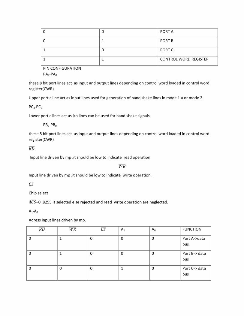
0 0 PORT A
0 1 PORT B
1 0 PORT C
1 1 CONTROL WORD REGISTER
PIN CONFIGURATION
PA7-PA0
these 8 bit port lines act as input and output lines depending on control word loaded in control word
register(CWR)
Upper port c line act as input lines used for generation of hand shake lines in mode 1 a or mode 2.
PC3-PC0
Lower port c lines act as i/o lines can be used for hand shake signals.
PB7-PB0
these 8 bit port lines act as input and output lines depending on control word loaded in control word
register(CWR)
������
Input line driven by mp .it should be low to indicate read operation
�������
Input line driven by mp .it should be low to indicate write operation.
������
Chip select
if������=0 ,8255 is selected else rejected and read write operation are neglected.
A1-A0
Adress input lines driven by mp.
������ ������� ������ A1 A0 FUNCTION
0 1 0 0 0 Port A->data
bus
0 1 0 0 0 Port B-> data
bus
0 0 0 1 0 Port C-> data
bus
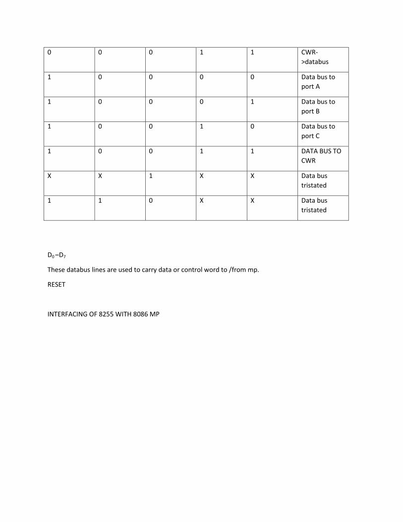
0 0 0 1 1 CWR-
>databus
1 0 0 0 0 Data bus to
port A
1 0 0 0 1 Data bus to
port B
1 0 0 1 0 Data bus to
port C
1 0 0 1 1 DATA BUS TO
CWR
X X 1 X X Data bus
tristated
1 1 0 X X Data bus
tristated
D0 –D7
These databus lines are used to carry data or control word to /from mp.
RESET
INTERFACING OF 8255 WITH 8086 MP
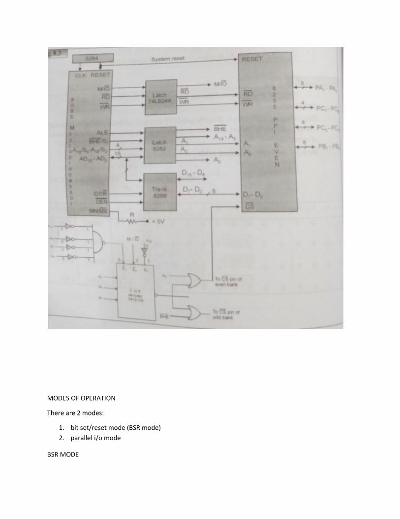
MODES OF OPERATION
There are 2 modes:
1. bit set/reset mode (BSR mode)
2. parallel i/o mode
BSR MODE
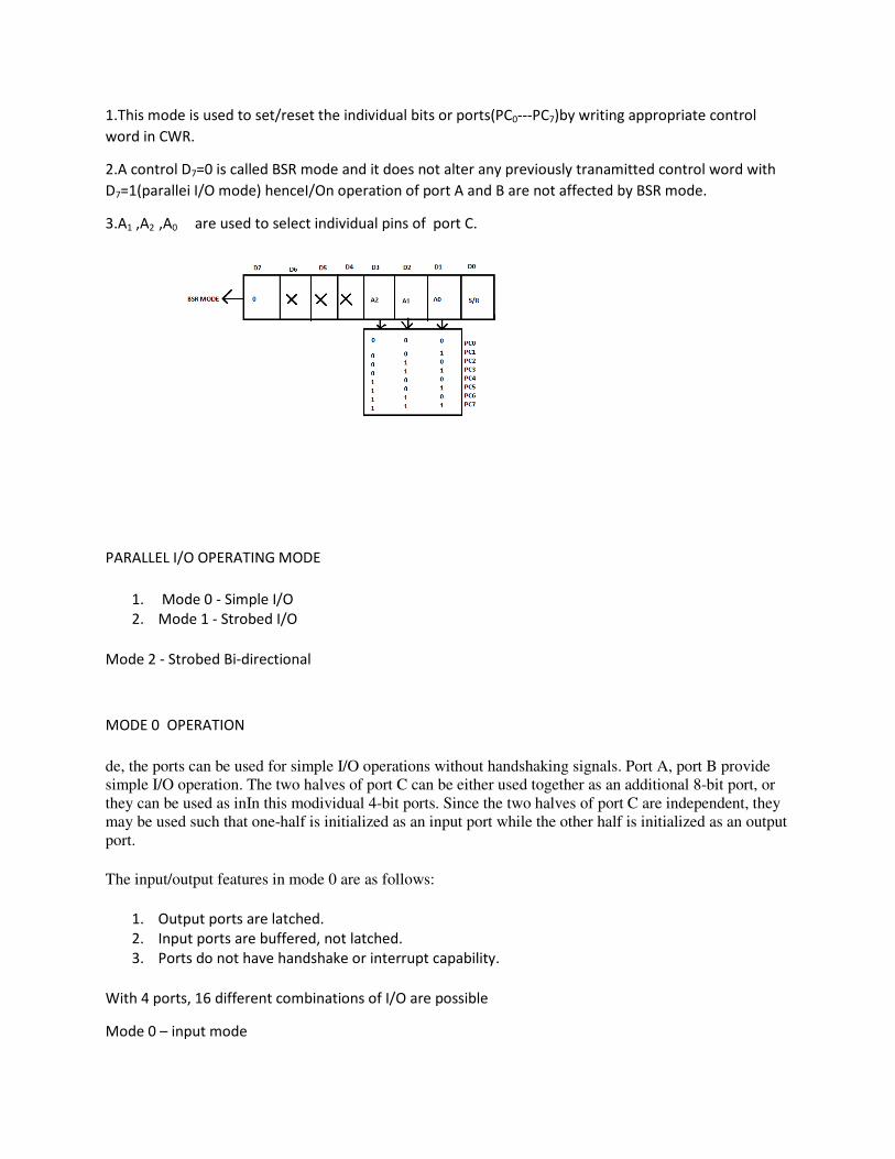
1.This mode is used to set/reset the individual bits or ports(PC0---PC7)by writing appropriate control
word in CWR.
2.A control D7=0 is called BSR mode and it does not alter any previously tranamitted control word with
D7=1(parallei I/O mode) henceI/On operation of port A and B are not affected by BSR mode.
3.A1 ,A2 ,A0 are used to select individual pins of port C.
PARALLEL I/O OPERATING MODE
1. Mode 0 - Simple I/O
2. Mode 1 - Strobed I/O
Mode 2 - Strobed Bi-directional
MODE 0 OPERATION
de, the ports can be used for simple I/O operations without handshaking signals. Port A, port B provide
simple I/O operation. The two halves of port C can be either used together as an additional 8-bit port, or
they can be used as inIn this modividual 4-bit ports. Since the two halves of port C are independent, they
may be used such that one-half is initialized as an input port while the other half is initialized as an output
port.
The input/output features in mode 0 are as follows:
1. Output ports are latched.
2. Input ports are buffered, not latched.
3. Ports do not have handshake or interrupt capability.
With 4 ports, 16 different combinations of I/O are possible
Mode 0 – input mode
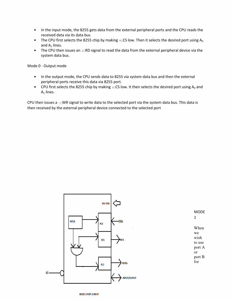
• In the input mode, the 8255 gets data from the external peripheral ports and the CPU reads the
received data via its data bus.
• The CPU first selects the 8255 chip by making CS low. Then it selects the desired port using A0
and A1 lines.
• The CPU then issues an RD signal to read the data from the external peripheral device via the
system data bus.
Mode 0 - Output mode
• In the output mode, the CPU sends data to 8255 via system data bus and then the external
peripheral ports receive this data via 8255 port.
• CPU first selects the 8255 chip by making CS low. It then selects the desired port using A0 and
A1 lines.
CPU then issues a WR signal to write data to the selected port via the system data bus. This data is
then received by the external peripheral device connected to the selected port
MODE
1
When
we
wish
to use
port A
or
port B
for
The image …
The image …
The image …
The image …
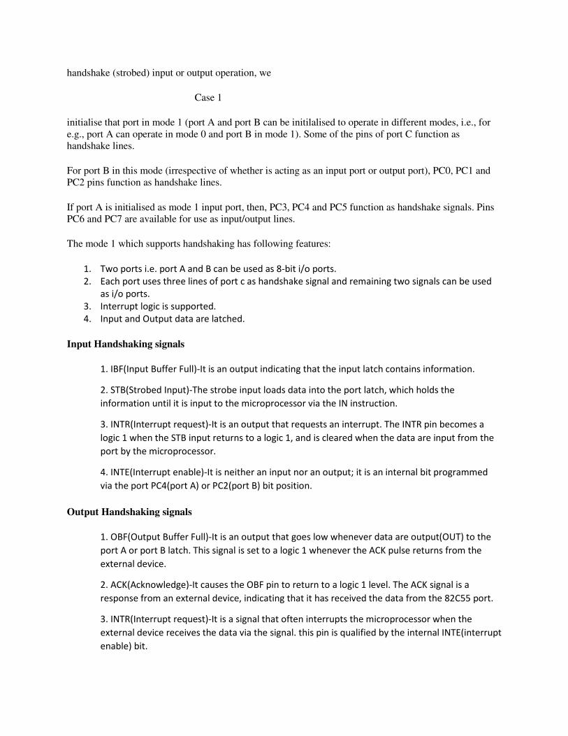
handshake (strobed) input or output operation, we
Case 1
initialise that port in mode 1 (port A and port B can be initilalised to operate in different modes, i.e., for
e.g., port A can operate in mode 0 and port B in mode 1). Some of the pins of port C function as
handshake lines.
For port B in this mode (irrespective of whether is acting as an input port or output port), PC0, PC1 and
PC2 pins function as handshake lines.
If port A is initialised as mode 1 input port, then, PC3, PC4 and PC5 function as handshake signals. Pins
PC6 and PC7 are available for use as input/output lines.
The mode 1 which supports handshaking has following features:
1. Two ports i.e. port A and B can be used as 8-bit i/o ports.
2. Each port uses three lines of port c as handshake signal and remaining two signals can be used
as i/o ports.
3. Interrupt logic is supported.
4. Input and Output data are latched.
Input Handshaking signals
1. IBF(Input Buffer Full)-It is an output indicating that the input latch contains information.
2. STB(Strobed Input)-The strobe input loads data into the port latch, which holds the
information until it is input to the microprocessor via the IN instruction.
3. INTR(Interrupt request)-It is an output that requests an interrupt. The INTR pin becomes a
logic 1 when the STB input returns to a logic 1, and is cleared when the data are input from the
port by the microprocessor.
4. INTE(Interrupt enable)-It is neither an input nor an output; it is an internal bit programmed
via the port PC4(port A) or PC2(port B) bit position.
Output Handshaking signals
1. OBF(Output Buffer Full)-It is an output that goes low whenever data are output(OUT) to the
port A or port B latch. This signal is set to a logic 1 whenever the ACK pulse returns from the
external device.
2. ACK(Acknowledge)-It causes the OBF pin to return to a logic 1 level. The ACK signal is a
response from an external device, indicating that it has received the data from the 82C55 port.
3. INTR(Interrupt request)-It is a signal that often interrupts the microprocessor when the
external device receives the data via the signal. this pin is qualified by the internal INTE(interrupt
enable) bit.
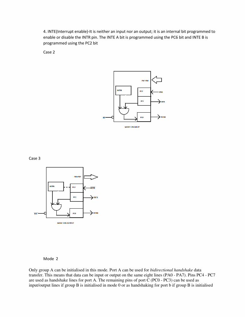
4. INTE(Interrupt enable)-It is neither an input nor an output; it is an internal bit programmed to
enable or disable the INTR pin. The INTE A bit is programmed using the PC6 bit and INTE B is
programmed using the PC2 bit
Case 2
Case 3
Mode 2
Only group A can be initialised in this mode. Port A can be used for bidirectional handshake data
transfer. This means that data can be input or output on the same eight lines (PA0 - PA7). Pins PC4 - PC7
are used as handshake lines for port A. The remaining pins of port C (PC0 - PC3) can be used as
input/output lines if group B is initialised in mode 0 or as handshaking for port b if group B is initialised

in mode 1. In this mode, the 8255 may be used to extend the system bus to a slave microprocessor or to
transfer data bytes to and from a floppy disk controller.
INTR
This is an output signal given or generated by 8255 generated by 8255.A high on this output signal can
be used to interupt the mp for both input and output..
INPUT OPERATION
1.����������(strobe input)
This is an active low input signal when peripheral write data to the input buffer the peripheral generates a
signal1.����������to indicate the 8255 that it has written data
2.IBF(input output full)
It is high in output signal and data loaded in the in larch and available in output buffer.
3.INTE1
This is an internal flip flop. Used in enable or disable interrupt signal.
OUTPUT OPERATION
1.�������
This is active low and indicates data is available in outpit data.
2.�� ������
It is put is active low and indicates output is empty.

3.INTE2
It is internal flip flop signal controlled by bit set reset mode using pc6 bit of part B. i
The Intel 8254 is a counter/timer device designed to solve the common timing control
problems in microcomputer system design. It provides three independent 16-bit counters, each
capable of handling clock inputs upto 10 MHz.All modesare software programmable. The 8254
is a superset of the 8253.The 8254 uses HMOS technology and comes in a 24-pin plastic or
CERDIPP PACKAGE.
PIN CONFIGURATION
rrrryrrrRPin Description
D7-D0 1-8 I/O-DATA: Bi-directional three state data bus lines,connected to
system data bus.
CLK 09 I- CLOCK 0: Clock input of Counter 0.
OUT 0 10O-OUTPUT 0: Output of Counter 0. GATE 0 11 I-GATE 0: Gate input of Counter 0.

GND 12 GROUND: Power supply connection. VCC 24POWER: a5V power supply connection.
WR 23 I WRITE CONTROL: This input is low during CPU write operations. RD 22 I READ CONTROL: This input is low during CPU read operations.
A1 A0 Selects 0 0 Counter 0 0 1Counter 1 10 Counter 2 1 1 Control Word Register CLK 2 18 I CLOCK 2: Clock input of Counter 2. OUT 2 17 O OUT 2: Output of Counter 2. GATE 2 16 I GATE 2: Gate input of Counter 2. CLK 1 15 I CLOCK 1: Clock input of Counter 1. GATE 1 14 I GATE 1: Gate input of Counter 1. OUT 1 13 O OUT 1: Output of Counter 1. FUNCTIONAL DESCRIPTION The 8254 is a programmable interval timer/counterdesigned for use with Intel microcomputer
systems.It is a general purpose, multi-timing element that canbe treated as an array of I/O ports
in the system
software.The 8254 solves one of the most common problems in any microcomputer system, the
generation of accuratetime delays under software control. Instead ofsetting up timing loops in
software, the programmerconfigures the 8254 to match his requirements and
programs one of the counters for the desired delay.After the desired delay, the 8254 will
interrupt theCPU. Software overhead is minimal and variablelength delays can easily be
accommodated.Some of the other counter/timer functions commonto microcomputers which can
be implemented withthe 8254 are:
# Real time clock
# Event-counter
# Digital one-shot
# Programmable rate generator
# Square wave generator
# Binary rate multiplier
# Complex waveform generator
# Complex motor controller
BLOCK DIAGRAM OF 8254

DATA BUS BUFFER This 3-state, bi-directional, 8-bit buffer is used to interface the 8254 to the system bus. READ/WRITE LOGIC The Read/Write Logic accepts inputs from the system bus and generates control signals for the otherfunctional blocks of the 8254. A1 and A0 select oneof the three counters or the Control Word Register to be read from/written into. A ``low'' on the RD inputtells the 8254 that the CPU is reading one of thecounters. A ``low'' on the WR input tells the 8254that the CPU is writing either a Control Word or aninitial count. Both RD and WR are qualified by CS;RD and WR are ignored unless the 8254 has beenselected by holding CS low. CONTROL WORD REGISTER The Control Word Register (see Figure 4) is selectedby the Read/Write Logic when A1,A0e11. If theCPU then does a write operation to the 8254, thedata is stored in the Control Word Register and isinterpreted as a Control Word used to define theoperation of the Counters.TheControl
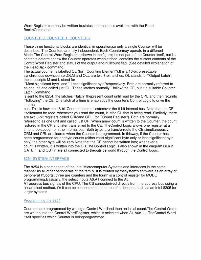
Word Register can only be written to;status information is available with the Read-BacknCommand. COUNTER 0, COUNTER 1, COUNTER 2 These three functional blocks are identical in operation,so only a single Counter will be described. The Counters are fully independent. Each Countermay operate in a different Mode.The Control Word Register is shown in the figure; itis not part of the Counter itself, but its contents determinehow the Counter operates whenlatched, contains the current contents of the ControlWord Register and status of the output and nullcount flag. (See detailed explanation of the ReadBack command.) The actual counter is labelled CE (for ``Counting Element'').It is a 16-bit presettable synchronous downcounter.OLM and OLL are two 8-bit latches. OL stands for``Output Latch''; the subscripts M and L stand for ``Most significant byte'' and ``Least significant byte''respectively. Both are normally referred to as oneunit and called just OL. These latches normally ``follow''the CE, but if a suitable Counter Latch Command is sent to the 8254, the latches ``latch'' thepresent count until read by the CPU and then returnto ``following'' the CE. One latch at a time is enabledby the counter's Control Logic to drive the internal bus. This is how the 16-bit Counter communicatesover the 8-bit internal bus. Note that the CE itselfcannot be read; whenever you read the count, it isthe OL that is being read. Similarly, there are two 8-bit registers called CRMand CRL (for ``Count Register''). Both are normally referred to as one unit and called just CR. When anew count is written to the Counter, the count isstored in the CR and later transferred to the CE. TheControl Logic allows one register at a time to beloaded from the internal bus. Both bytes are transferredto the CE simultaneously. CRM and CRL arecleared when the Counter is programmed. In thisway, if the Counter has been programmed for onebyte counts (either most significant byte only or leastsignificant byte only) the other byte will be zero.Note that the CE cannot be written into; whenever a count is written, it is written into the CR.The Control Logic is also shown in the diagram.CLK n, GATE n, and OUT n are all connected to theoutside world through the Control Logic. 8254 SYSTEM INTERFACE The 8254 is a component of the Intel Microcomputer Systems and interfaces in the same manner as all other peripherals of the family. It is treated by thesystem's software as an array of peripheral I/Oports; three are counters and the fourth is a control register for MODE programming.Basically, the select inputs A0,A1 connect to the A0, A1 address bus signals of the CPU. The CS canbederived directly from the address bus using a linearselect method. Or it can be connected to the outputof a decoder, such as an Intel 8205 for larger systems
Programming the 8254 Counters are programmed by writing a Control Wordand then an initial count.The Control Words are written into the Control WordRegister, which is selected when A1,A0e 11. TheControl Word itself specifies which Counter is beingprogrammed.
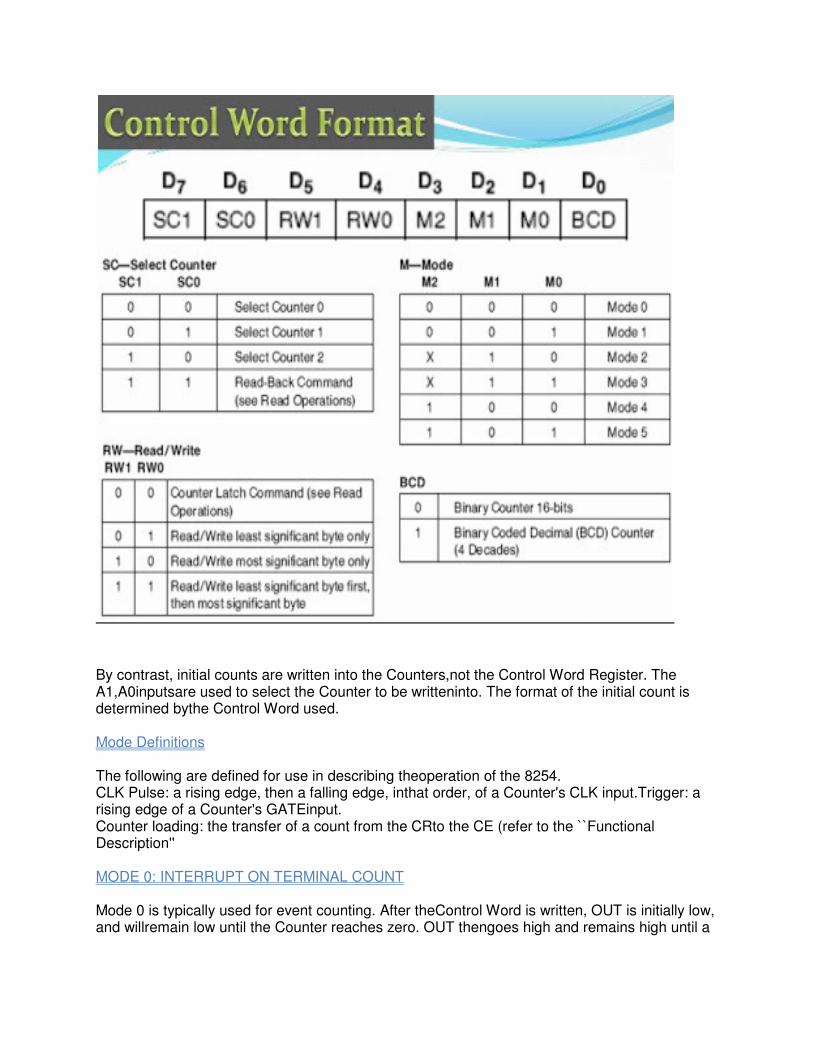
By contrast, initial counts are written into the Counters,not the Control Word Register. The A1,A0inputsare used to select the Counter to be writteninto. The format of the initial count is determined bythe Control Word used. Mode Definitions The following are defined for use in describing theoperation of the 8254. CLK Pulse: a rising edge, then a falling edge, inthat order, of a Counter's CLK input.Trigger: a rising edge of a Counter's GATEinput. Counter loading: the transfer of a count from the CRto the CE (refer to the ``Functional Description'' MODE 0: INTERRUPT ON TERMINAL COUNT Mode 0 is typically used for event counting. After theControl Word is written, OUT is initially low, and willremain low until the Counter reaches zero. OUT thengoes high and remains high until a
new count or anew Mode 0 Control Word is written into the Counter.GATEe 1 enables counting; GATE e 0 disablescounting. GATE has no effect on OUT. After the Control Word and initial count are written toa Counter, the initial count will be loaded on the nextCLK pulse. This CLK pulse does not decrement thecount, so for an initial count of N, OUT does not gohigh until N a 1 CLK pulses after the initial count iswritten.If a new count is written to the Counter, it will beloaded on the next CLK pulse and counting will continuefrom the new count. If a two-byte count is written, the following happens: 1) Writing the first byte disables counting. OUT is setlow immediately (no clock pulse required) 2) Writing the second byte allows the new count tobe loaded on the next CLK pulse. This allows the counting sequence to be synchronizedby software. Again, OUT does not go high untilNa1 CLK pulses after the new count of N is written.If an initial count is written while GATE e 0, it will still be loaded on the next CLK pulse. When GATEgoes high, OUT will go high N CLK pulses later; noCLK pulse is needed to load the Counter as this hasalready been done. MODE 1: HARDWARE RETRIGGERABLE ONE-SHOT OUT will be initially high. OUT will go low on the CLKpulse following a trigger to begin the one-shot pulse,and will remain low until the Counter reaches zero. OUT will then go high and remain high until the CLKpulseafter the next trigger.After writing the Control Word and initial count, theCounter is armed. A trigger results in loading theCounter and setting OUT low on the next CLK pulse,thus starting the one-shot pulse. An initial count of Nwill result in a one-shot pulse N CLK cycles in duration. The one-shot is retriggerable, hence OUT willremain low for N CLK pulses after any trigger. Theone-shot pulse can be repeated without rewriting thesame count into the counter. GATE has no effect on OUT.If a new count is written to the Counter during aoneshotpulse, the current one-shot is not affected unlessthe counter is retriggered. In that case, theCounter is loaded with the new count and the oneshotpulse continues until the new count expires. MODE 2: RATE GENERATOR This Mode functions like a divide-by-N counter. It is typically used to generate a Real Time Clock interrupt.OUT will initially be high. When the initial counthas decremented to 1, OUT goes low for one CLKpulse. OUT then goes high again, the Counter reloadsthe initial count and the process is repeated.Mode 2 is periodic; the same sequence is repeated indefinitely. For an initial count of N, the sequencerepeats every N CLK cycles.GATEe1 enables counting; GATE e 0 disablescounting. If GATE goes low during an output pulse,OUT is set high immediately. A trigger reloads theCounter with the initial count on the next CLK pulse; OUT goes low N CLK pulses after the trigger. Thusthe GATE input can be used to synchronize theCounter.After writing a Control Word and initial count, theCounter will be loaded on the next CLK pulse. OUTgoes low N CLK Pulses after the initial count is written.This allows the Counter to be synchronized bysoftwarealso.Writing a new count while counting does not affectthe current counting sequence. If a trigger is receivedafter writing a new count but before the endof the current period, the Counter will be loaded withthe new count on the next CLK pulse and countingwill continue from the new count. Otherwise, thenew count will be loaded at the end of the currentcounting cycle. In mode 2, a COUNT of 1 is illegal. MODE 3: SQUARE WAVE MODE

Mode 3 is typically used for Baud rate generation.Mode 3 is similar to Mode 2 except for the duty cycleof OUT. OUT will initially be high. When half the initial count has expired, OUT goes low for the remainderof the count. Mode 3 is periodic; the sequenceabove is repeated indefinitely. An initialcount of N results in a square wave with a period ofN CLK cycles.GATEe1 enables counting; GATE e 0 disablescounting. If GATE goes low while OUT is low, OUT isset high immediately; no CLK pulse is required. Atrigger reloads the Counter with the initial count on the next CLK pulse. Thus the GATE input canbeused to synchronize the Counter. After writing a Control Word and initial count, theCounter will be loaded on the next CLK pulse. Thisallows the Counter to be synchronized by softwarealso.Writing a new count while counting does not affectthe current counting sequence. If a trigger is receivedafter writing a new count but before the endof the current half-cycle of the square wave, theCounter will be loaded with the new count on the next CLK pulse and counting will continue from the new count. Otherwise, the new count will be loadedat the end of the current half-cycle.Mode 3 is implemented as follows:Even counts: OUT is initially high. The initial count isloaded on one CLK pulse and then is decrementedby two on succeeding CLK pulses. When the count expires OUT changes value and the Counter is reloadedwith the initial count. The above process isrepeated indefinitely. Odd counts: OUT is initially high. The initial countminus one (an even number) is loaded on one CLKpulse and then is decremented by two on succeedingCLK pulses. One CLK pulse after the count expires,OUT goes low and the Counter is reloadedwith the initial count minus one. Succeeding CLKpulses decrement the count by two. When the countexpires, OUT goes high again and the Counter isreloaded with the initial count minus one. The aboveprocess is repeated indefinitely. So for odd counts,OUT will be high for (N a 1)/2 counts and low for(N b 1)/2 counts. MODE 4: SOFTWARE TRIGGERED STROBE OUT will be initially high. When the initial count expires,OUT will go low for one CLK pulse and thengo high again. The counting sequence is ``triggered''by writing the initial count.GATEe1 enables counting; GATE e 0 disablescounting. GATE has no effect on OUT.After writing a Control Word and initial count, theCounter will be loaded on the next CLK pulse. ThisCLK pulse does not decrement the count, so for an initial count of N, OUT does not strobe low until N a1 CLK pulses after the initial count is written.If a new count is written during counting, it will beloaded on the next CLK pulse and counting will continuefrom the new count. If a two-byte count is written,the following happens: 1) Writing the first byte has no effect on counting. 2) Writing the second byte allows the new count to be loaded on the next CLK pulse.This allows the sequence to be ``retriggered'' bysoftware. OUT strobes low N a 1 CLK pulses after the new count of N is written.231164±11 MODE 5: HARDWARE TRIGGERED STROBE (RETRIGGERABLE)

OUT will initially be high. Counting is triggered by arising edge of GATE. When the initial count has expired,OUT will go low for one CLK pulseandthengo high again.After writing the Control Word and initial count, thecounter will not be loaded until the CLK pulse after atrigger. This CLK pulse does not decrement thecount, so for an initial count of N, OUT does notstrobe low until N a 1 CLK pulses after a trigger. A trigger results in the Counter being loaded with theinitial count on the next CLK pulse. The countingsequence is retriggerable. OUT will not strobe lowfor N a 1 CLK pulses after any trigger. GATE hasno effect on OUT.If a new count is written during counting, the currentcounting sequence will not be affected. If a trigger occurs after the new count is written but before thecurrent count expires, the Counter will be loadedwith the new count on the next CLK pulse andcounting will continue from there. READ-BACK COMMAND The third method uses the Read-Back Command.This command allowsthe user to check the countvalue, programmed Mode, and currentstates of the OUT pin and Null Count flag of the selected counter(s).Thecommand applies to the counters selected by settingtheir corresponding bits D3, D2, D1 e 1. The read-back command maybe used to latch multiplecounter output latches (OL) by setting the COUNT bit D5 e 0 and selecting the desired counter(s). This single command is functionally equivalentto several counter latch commands, one foreach counter latched. Each counter's latched countis held until it is read (or the counter is reprogrammed).The counter is automatically unlatchedwhen read, but other counters remain latched until they are read. If multiple count read-back commandsare issued to the same counter without reading thecount, all but the first are ignored; i.e., the countwhich will be read is the count at the time the first read-back command was issued.The read-back command may also be used to latchstatus information of selected counter(s) by settingSTATUS bit D4 e 0. Status must be latched to beread; status of a counter is accessed by a read fromthatcounter.The counter status format is shown in Figure 11. BitsD5 through D0 contain the counter's programmedMode exactly as written in the last Mode ControlWord. OUTPUT bit D7 contains thecurrent state ofthe OUT pin. This allows the user to monitor thecounter's output via software, possibly eliminating some hardware from a system.
DIRECT MEMORY ACCESS CONTROLER 8237
The 8237A Multimode Direct Memory Access (DMA) Controller is a peripheral interface circuit for microprocessorsystems. It is designed to improve system performance by allowing external devices to directly transferinformation from the system memory. Memory-to-memory transfer capability is also provided. The 8237A offers a wide variety of programmable control features to enhance data throughput and system optimizationand to allow dynamic reconfiguration under program control. The 8237A is designed to be used in conjunction with an external 8-bit address latch. It contains four independent
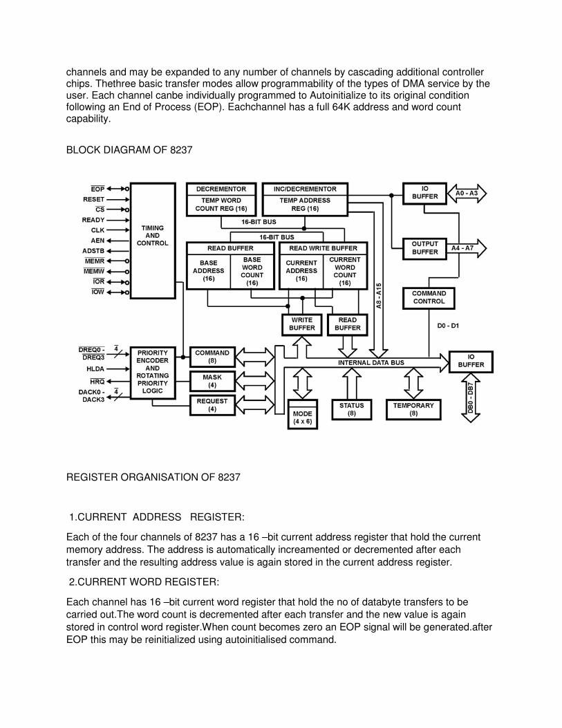
channels and may be expanded to any number of channels by cascading additional controller chips. Thethree basic transfer modes allow programmability of the types of DMA service by the user. Each channel canbe individually programmed to Autoinitialize to its original condition following an End of Process (EOP). Eachchannel has a full 64K address and word count capability.
BLOCK DIAGRAM OF 8237
REGISTER ORGANISATION OF 8237
1.CURRENT ADDRESS REGISTER:
Each of the four channels of 8237 has a 16 –bit current address register that hold the current
memory address. The address is automatically increamented or decremented after each
transfer and the resulting address value is again stored in the current address register.
2.CURRENT WORD REGISTER:
Each channel has 16 –bit current word register that hold the no of databyte transfers to be
carried out.The word count is decremented after each transfer and the new value is again
stored in control word register.When count becomes zero an EOP signal will be generated.after
EOP this may be reinitialized using autoinitialised command.
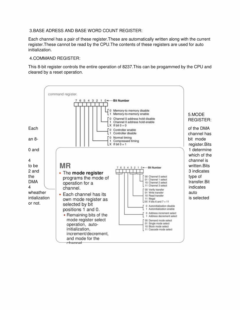
3.BASE ADRESS AND BASE WORD COUNT REGISTER:
Each channel has a pair of these register.These are automatically written along with the current
register.These cannot be read by the CPU.The contents of these registers are used for auto
initialization.
4.COMMAND REGISTER:
This 8-bit register controls the entire operation of 8237.This can be progammed by the CPU and
cleared by a reset operation.
5.MODE
REGISTER:
Each of the DMA
channel has
an 8- bit mode
register.Bits
0 and 1 determine
which of the
4 channel is
to be written.Bits
2 and 3 indicates
the type of
DMA transfer.Bit
4 indicates
wheather auto
intialization is selected
or not.
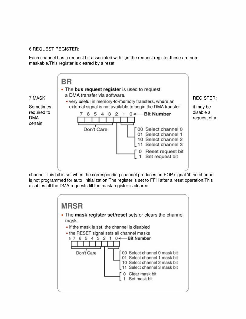
6.REQUEST REGISTER:
Each channel has a request bit associated with it,in the request register.these are non-
maskable.This register is cleared by a reset.
7.MASK REGISTER:
Sometimes it may be
required to disable a
DMA request of a
certain
channel.This bit is set when the corresponding channel produces an EOP signal ‘if the channel
is not programmed for auto initialization.The register is set to FFH after a reset operation.This
disables all the DMA requests till the mask register is cleared.

8.STATUS REGISTER:
The status register keeps the track of all the DMA channel pending requests and status of their
terminal counts.The bits d0 –d3 are set every time ,the corresponding channel reaches TC.These
are cleared upon reset and also on each status read operation.Bits d4-d7 are set,if the
corresponding
channel request
service
PIN
CONFIGURATION
OF 8237
PIN
DESCRIPTION
CLOCK :Clock Input controls the internal operations of the8237A and its rate of data transfers.
The input may be driven at upto 5 MHz for the 8237A-5.
������: Chip Select is an active low input used to selectthe 8237A as an I/O device during the Idle cycle. This allows CPUcommunication on the data bus RESET: Reset is an active high input which clears the Command,Status, Request and Temporary registers. It also clears the first/last flip/flop and sets the Mask register. Following a Reset thedevice is in the Idle cycle. READY: Ready is an input used to extend the memory read andwrite pulses from the 8237A to accommodate slow memories orI/O peripheral devices. Ready must not make transitions during itsspecified setup/hold time . HOLD ACKNOWLEDGE: The active high Hold Acknowledge fromthe CPU indicates that it has relinquished control of the system DMA REQUEST: The DMA Request lines are individualasynchronous channel request inputs used by peripheral circuitstoobtain DMA service. In fixed Priority, DREQ0 has the highestpriority and DREQ3 has the lowest priority. A request is generatedby activating the DREQ line of a channel. DACK will acknowledge the recognition of DREQ signal. Polarity of DREQ isprogrammable. Reset initializes these lines to active high. DREQmust be maintained until the corresponding DACK goes active. DATA BUS: The Data Bus lines are bidirectional three-statesignals connected to the system data bus. The outputs areenabled in the Program condition during the I/O Read to outputthe contents of an Address register, a Status register, theTemporary register or a Word Count register to the CPU. Theoutputs are disabled and the inputs are read during an I/O Writecycle when the CPU is programming the 8237A control registers.During DMA cycles the most significant 8 bits of the address are output onto the data bus to be strobed into an external latch byADSTB. In memory-to-memory operations, data from the memorycomes into the 8237A on the data bus during the read-frommemorytransfer. In the write-to-memory transfer, the data busoutputs place the data �������: I/O Read is a bidirectional active low three-state line.In the Idle cycle, it is an input control signal used by the CPU toread the control registers. In the Active cycle, it is an output controlsignal used by the 8237A to access data from a peripheral during aDMA Write transfer. ��������: I/O Write is a bidirectional active low three-state line.In the Idle cycle, it is an input control signal used by the CPU toload information into the 8237A. In the Active cycle, it is an outputcontrol signal used by the 8237A to load data to the peripheral during a DMA Read transfer.
��������:End of Process is an active low bidirectionalsignal. Information concerning the completion of DMA services isavailable at the bidirectional EOP pin. The 8237A allows anexternal signal to terminate an active DMA service. This isaccomplished by pulling the EOP input low with an external EOPsignal. The 8237A also generates a pulse when the terminal count(TC) for any channel is reached. This generates an EOP signalwhich is output through the EOP line. The

reception of EOP, eitherinternal or external, will cause the 8237A to terminate the service,reset the request, and, if Autoinitialize is enabled, to write the baseregisters to the current registers of that channel. The mask bit andTC bit in the status word will be set for the currently active channelby EOP unless the channel is programmed for Autoinitialize. In thatcase, the mask bit remains unchanged. During memory-to-memorytransfers, EOP will be output when the TC for channel 1 occurs.EOP should be tied high with a pull-up resistor if it is not used toprevent erroneous end of process inputs. A0 –A3:The four least significant address lines arebidirectional three-state signals. In the Idle cycle they are inputsand are used by the CPU to address the register to be loaded orread. In the Active cycle they are outputs and provide the lower 4bits of the output address. A4 – A7: The four most significant address lines are three-stateoutputs and provide 4 bits of address. These lines are enabledonly during the DMA service. HRQ :This is the Hold Request to the CPU and isused to request control of the system bus. If the correspondingmask bit is clear, the presence of any valid DREQ causes 8237A toissue the HRQ. DACK0 –DACK3 :DMA Acknowledge is used to notify theindividual peripherals when one has been granted a DMA cycle.The sense of these lines is programmable. AEN :Address Enable enables the 8-bit latchcontaining the upper 8 address bits onto the system address bus.AEN can also be used to disable other system bus drivers duringDMA transfers. AEN is active HIGH. �������������:The Memory Read signal is an active low threestateoutput used to access data from the selected memorylocation during a DMA Read or a memory-to-memory transfer. ��������������:The Memory Write is an active low three-stateoutput used to write data to the selected memory location during aDMA Write or a memory-to-memory transfer. PIN5: This pin should always be at a logic HIGH level. An internalpull-up resistor will establish a logic high when the pin is leftfloating. It is recommended however, that PIN5 be connected toVCC. MODE OF OPERATION OF 8237
SINGLE TRANSFER MODE In Single Transfer modethe device is programmed to make one transfer only.The word count will be decremented and the addressdecremented or incremented following eachtransfer. When the word count ``rolls over'' from zero to FFFFH, a Terminal Count (TC) will cause an Autoinitializeif the channel has been programmed to doso.DREQ must be held active until DACK becomes activein order to be
recognized. If DREQ is held activethroughout the single transfer, HRQ will go inactiveand release the bus to the system. It will again goactive and, upon receipt of a new HLDA, anothersingle transfer will be performed. In 8080A, 8085AH, 8088, or 8086 system, this will ensure one full machinecycle execution between DMA transfers. Detailsof timing between the 8237A and other buscontrol protocols will depend upon the characteristicsof the microprocessor involved. BLOCK TRANSFER MODE In Block Transfer mode thedevice is activated by DREQ to continue makingtransfers during the service until a TC, caused byword count going to FFFFH, or an external End ofProcess (EOP) is encountered. DREQ need only be held active until DACK becomes active. Again, anAutoinitialization will occur at the end of the serviceif the channel has been programmed for it. DEMAND TRANSFER MODE In Demand Transfermode the device is programmed to continue makingtransfers until a TC or external EOP is encounteredor until DREQ goes inactive. Thus transfers maycontinue until the I/O device has exhausted its datacapacity. After the I/O device has had a chance tocatch up, the DMA service is re-established bymeans of a DREQ. During the time between services when the microprocessor is allowed to operate, theintermediate values of address and word count arestored in the 8237A Current Address and CurrentWord Count registers. Only an EOP can cause anAutoinitialize at the end of the service. EOP is generatedeither by TC or by an external signal. DREQhas to be low before S4 to prevent another Transfer. CASCADE MODE This mode is used to cascademore than one 8237A together for simple systemexpansion. The HRQ and HLDA signals from the additional8237A are connected to the DREQ andDACK signals of a channel of the initial 8237A. Thisallows the DMA requests of the additional device topropagate through the priority network circuitry ofthe preceding device. The priority chain is preservedand the new device must wait for its turn to acknowledgerequests. Since the cascade channel of theinitial 8237A is used only for prioritizing the additionaldevice, it does not output any address or control. INTERFACING OF 8237 WITH 8086
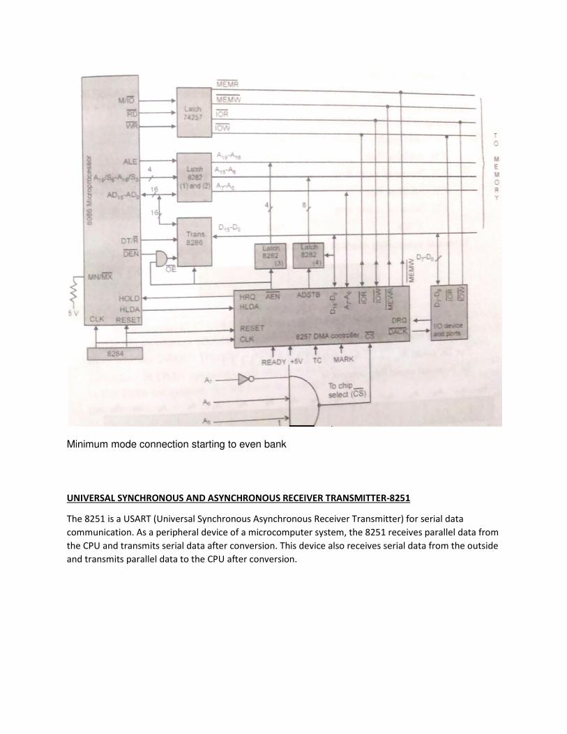
Minimum mode connection starting to even bank
UNIVERSAL SYNCHRONOUS AND ASYNCHRONOUS RECEIVER TRANSMITTER-8251
The 8251 is a USART (Universal Synchronous Asynchronous Receiver Transmitter) for serial data
communication. As a peripheral device of a microcomputer system, the 8251 receives parallel data from
the CPU and transmits serial data after conversion. This device also receives serial data from the outside
and transmits parallel data to the CPU after conversion.

Block diagram of the 8251 USART (Universal Synchronous Asynchronous Receiver Transmitter)
The 8251 functional configuration is programed by software. Operation between the 8251 and a CPU is
executed by program control. Table 1 shows the operation between a CPU and the device.

Table 1 Operation between a CPU and 8251
C0NTROL WORD FORMAT-
There are two types of control word.
1. Mode instruction (setting of function)
2. Command (setting of operation)
1) MODE INSTRUCTION FORMAT-
Mode instruction is used for setting the function of the 8251. Mode instruction will be in "wait for write"
at either internal reset or external reset. That is, the writing of a control word after resetting will be
recognized as a "mode instruction."
Items set by mode instruction are as follows:
• Synchronous/asynchronous mode
• Stop bit length (asynchronous mode)
• Character length
• Parity bit
• Baud rate factor (asynchronous mode)
• Internal/external synchronization (synchronous mode)
• Number of synchronous characters (Synchronous mode)

The bit configuration of mode instruction is shown in Figures 2 and 3. In the case of synchronous mode,
it is necessary to write one-or two byte sync characters. If sync characters were written, a function will
be set because the writing of sync characters constitutes part of mode instruction.

2) COMMAND WORD REGISTER FORMAT-
Command is used for setting the operation of the 8251. It is possible to write a command whenever
necessary after writing a mode instruction and sync characters.
Items to be set by command are as follows:
• Transmit Enable/Disable
• Receive Enable/Disable
• DTR, RTS Output of data.
• Resetting of error flag.
• Sending to break characters
• Internal resetting
• Hunt mode (synchronous mode)
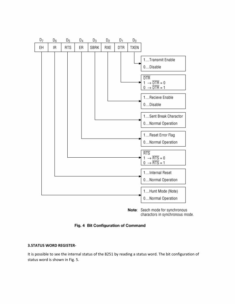
3.STATUS WORD REGISTER-
It is possible to see the internal status of the 8251 by reading a status word. The bit configuration of
status word is shown in Fig. 5.

PIN DESCRIPTION-

D 0 to D 7 (l/O terminal)
This is bidirectional data bus which receive control words and transmits data from the CPU and sends
status words and received data to CPU.
RESET (Input terminal)
A "High" on this input forces the 8251 into "reset status." The device waits for the writing of "mode
instruction." The min. reset width is six clock inputs during the operating status of CLK.
CLK (Input terminal)
CLK signal is used to generate internal device timing. CLK signal is independent of RXC or TXC. However,
the frequency of CLK must be greater than 30 times the RXC and TXC at Synchronous mode and
Asynchronous "x1" mode, and must be greater than 5 times at Asynchronous "x16" and "x64" mode.
WR (Input terminal)
This is the "active low" input terminal which receives a signal for writing transmit data and control words
from the CPU into the 8251.
RD (Input terminal)
This is the "active low" input terminal which receives a signal for reading receive data and status words
from the 8251.
C/D (Input terminal)

This is an input terminal which receives a signal for selecting data or command words and status words
when the 8251 is accessed by the CPU. If C/D = low, data will be accessed. If C/D = high, command word
or status word will be accessed.
CS (Input terminal)
This is the "active low" input terminal which selects the 8251 at low level when the CPU accesses. Note:
The device won’t be in "standby status"; only setting CS = High.
TXD (output terminal)
This is an output terminal for transmitting data from which serial-converted data is sent out. The device
is in "mark status" (high level) after resetting or during a status when transmit is disabled. It is also
possible to set the device in "break status" (low level) by a command.
TXRDY (output terminal)
This is an output terminal which indicates that the 8251is ready to accept a transmitted data character.
But the terminal is always at low level if CTS = high or the device was set in "TX disable status" by a
command. Note: TXRDY status word indicates that transmit data character is receivable, regardless of
CTS or command. If the CPU writes a data character, TXRDY will be reset by the leading edge or WR
signal.
TXEMPTY (Output terminal)
This is an output terminal which indicates that the 8251 has transmitted all the characters and had no
data character. In "synchronous mode," the terminal is at high level, if transmit data characters are no
longer remaining and sync characters are automatically transmitted. If the CPU writes a data character,
TXEMPTY will be reset by the leading edge of WR signal. Note : As the transmitter is disabled by setting
CTS "High" or command, data written before disable will be sent out. Then TXD and TXEMPTY will be
"High". Even if a data is written after disable, that data is not sent out and TXE will be "High".After the
transmitter is enabled, it sent out.
TXC (Input terminal)
This is a clock input signal which determines the transfer speed of transmitted data. In "synchronous
mode," the baud rate will be the same as the frequency of TXC. In "asynchronous mode", it is possible to
select the baud rate factor by mode instruction. It can be 1, 1/16 or 1/64 the TXC. The falling edge of
TXC sifts the serial data out of the 8251.
RXD (input terminal)
This is a terminal which receives serial data.
RXRDY (Output terminal)
This is a terminal which indicates that the 8251 contains a character that is ready to READ. If the CPU
reads a data character, RXRDY will be reset by the leading edge of RD signal. Unless the CPU reads a data
character before the next one is received completely, the preceding data will be lost. In such a case, an
overrun error flag status word will be set.
RXC (Input terminal)
This is a clock input signal which determines the transfer speed of received data. In "synchronous
mode," the baud rate is the same as the frequency of RXC. In "asynchronous mode," it is possible to
select the baud rate factor by mode instruction. It can be 1, 1/16, 1/64 the RXC.
SYNDET/BD (Input or output terminal)
This is a terminal whose function changes according to mode. In "internal synchronous mode." this
terminal is at high level, if sync characters are received and synchronized. If a status word is read, the
terminal will be reset. In "external synchronous mode, "this is an input terminal. A "High" on this input
forces the 8251 to start receiving data characters.
In "asynchronous mode," this is an output terminal which generates "high level"output upon the
detection of a "break" character if receiver data contains a "low-level" space between the stop bits of
two continuous characters. The terminal will be reset, if RXD is at high level. After Reset is active, the
terminal will be output at low level.
DSR (Input terminal)
This is an input port for MODEM interface. The input status of the terminal can be recognized by the
CPU reading status words.
DTR (Output terminal)
This is an output port for MODEM interface. It is possible to set the status of DTR by a command.
CTS (Input terminal)
This is an input terminal for MODEM interface which is used for controlling a transmit circuit. The
terminal controls data transmission if the device is set in "TX Enable" status by a command. Data is
transmitable if the terminal is at low level.
RTS (Output terminal)
This is an output port for MODEM interface. It is possible to set the status RTS by a command.
INTERFACING 8251 USART WITH 8086 MICROPROCESSOR-
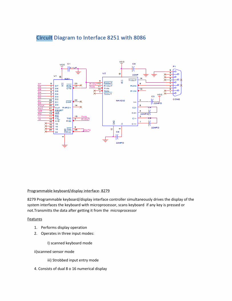
Programmable keyboard/display interface- 8279
8279 Programmable keyboard/display interface controller simultaneously drives the display of the
system interfaces the keyboard with microprocessor, scans keyboard if any key is pressed or
not.Transmitts the data after getting it from the microprocessor
Features
1. Performs display operation
2. Operates in three input modes:
I) scanned keyboard mode
ii)scanned sensor mode
iii) Strobbed input entry mode
4. Consists of dual 8 o 16 numerical display
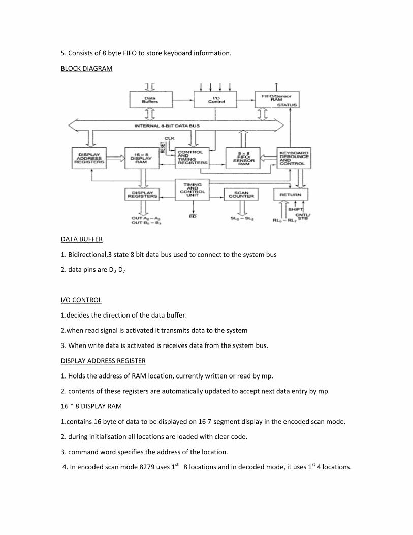
5. Consists of 8 byte FIFO to store keyboard information.
BLOCK DIAGRAM
DATA BUFFER
1. Bidirectional,3 state 8 bit data bus used to connect to the system bus
2. data pins are D0-D7
I/O CONTROL
1.decides the direction of the data buffer.
2.when read signal is activated it transmits data to the system
3. When write data is activated is receives data from the system bus.
DISPLAY ADDRESS REGISTER
1. Holds the address of RAM location, currently written or read by mp.
2. contents of these registers are automatically updated to accept next data entry by mp
16 * 8 DISPLAY RAM
1.contains 16 byte of data to be displayed on 16 7-segment display in the encoded scan mode.
2. during initialisation all locations are loaded with clear code.
3. command word specifies the address of the location.
4. In encoded scan mode 8279 uses 1st
8 locations and in decoded mode, it uses 1st
4 locations.
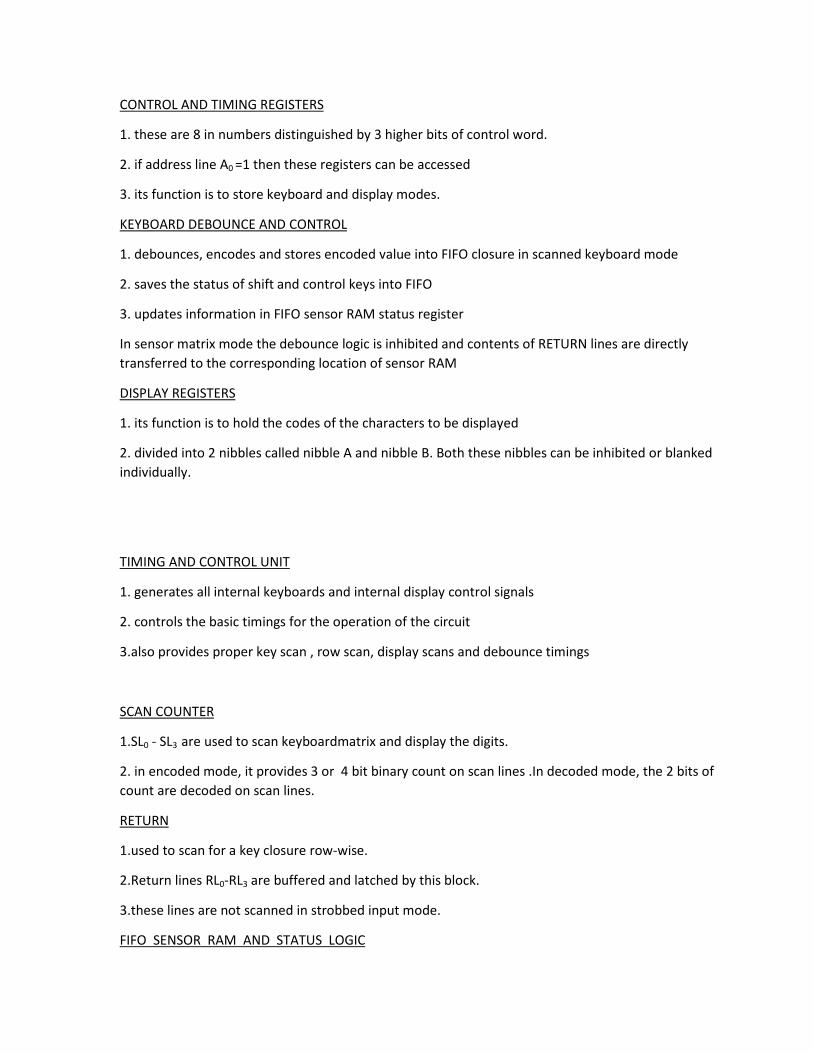
CONTROL AND TIMING REGISTERS
1. these are 8 in numbers distinguished by 3 higher bits of control word.
2. if address line A0 =1 then these registers can be accessed
3. its function is to store keyboard and display modes.
KEYBOARD DEBOUNCE AND CONTROL
1. debounces, encodes and stores encoded value into FIFO closure in scanned keyboard mode
2. saves the status of shift and control keys into FIFO
3. updates information in FIFO sensor RAM status register
In sensor matrix mode the debounce logic is inhibited and contents of RETURN lines are directly
transferred to the corresponding location of sensor RAM
DISPLAY REGISTERS
1. its function is to hold the codes of the characters to be displayed
2. divided into 2 nibbles called nibble A and nibble B. Both these nibbles can be inhibited or blanked
individually.
TIMING AND CONTROL UNIT
1. generates all internal keyboards and internal display control signals
2. controls the basic timings for the operation of the circuit
3.also provides proper key scan , row scan, display scans and debounce timings
SCAN COUNTER
1.SL0 - SL3 are used to scan keyboardmatrix and display the digits.
2. in encoded mode, it provides 3 or 4 bit binary count on scan lines .In decoded mode, the 2 bits of
count are decoded on scan lines.
RETURN
1.used to scan for a key closure row-wise.
2.Return lines RL0-RL3 are buffered and latched by this block.
3.these lines are not scanned in strobbed input mode.
FIFO SENSOR RAM AND STATUS LOGIC
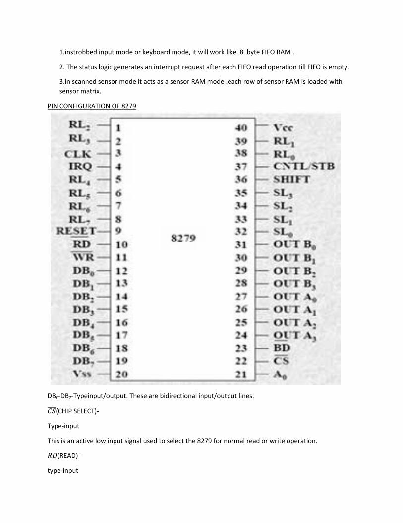
1.instrobbed input mode or keyboard mode, it will work like 8 byte FIFO RAM .
2. The status logic generates an interrupt request after each FIFO read operation till FIFO is empty.
3.in scanned sensor mode it acts as a sensor RAM mode .each row of sensor RAM is loaded with
sensor matrix.
PIN CONFIGURATION OF 8279
DB0-DB7-Typeinput/output. These are bidirectional input/output lines.
������(CHIP SELECT)-
Type-input
This is an active low input signal used to select the 8279 for normal read or write operation.
������(READ) -
type-input

This is an active low signal and a low on this i/p enables the 8279 to send data to the MP.
�������
When this pin is low MP will write data or control words into the 8279.
A0-When it is high it indicates the transfer of a command or status info. and when this is low it indicates
the transfer of data.
CLK-
Used to generate internal timings required by 8279.
RESET-
During reset the clock presale is set to 31.
IRQ-
When there is a data in FIFO sensor RAM the interrupt o/p goes high.
SL0-SL3-
Used to scan the keyboard matrix and display digits.
RL0-RL7-
These lines are connected to one terminal of keys while the other terminal is connected to the decoded
scan lines.
SHIFT-
In the scanned keyboard mode the status of the shift i/p line is stored along with each keys code in FIFO.
CNTL/STB-
Used as control i/p in the keyboard mode and stored in FIFO on a key closer.
�����
The o/ p pin is used to blank the display during the digit switching or by blanking display command.
OUTA0-OUTA3 and OUTB0-OUTB3-
These pins will work as the o/p ports .To scan the display & keyboard the data from these lines is
synchronised with the scan lines.
VCC-
This pin is used to provide power supply.
GND-
This pin is used to provide ground.
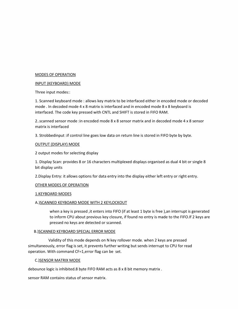
MODES OF OPERATION
INPUT (KEYBOARD) MODE
Three input modes::
1. Scanned keyboard mode : allows key matrix to be interfaced either in encoded mode or decoded
mode . In decoded mode 4 x 8 matrix is interfaced and in encoded mode 8 x 8 keyboard is
interfaced. The code key pressed with CNTL and SHIFT is stored in FIFO RAM.
2..scanned sensor mode :in encoded mode 8 x 8 sensor matrix and in decoded mode 4 x 8 sensor
matrix is interfaced
3. Strobbedinput :if control line goes low data on return line is stored in FIFO byte by byte.
OUTPUT (DISPLAY) MODE
2 output modes for selecting display
1. Display Scan: provides 8 or 16 characters multiplexed displays organised as dual 4 bit or single 8
bit display units
2.Display Entry: it allows options for data entry into the display either left entry or right entry.
OTHER MODES OF OPERATION
1.KEYBOARD MODES
A.)SCANNED KEYBOARD MODE WITH 2 KEYLOCKOUT
when a key is pressed ,it enters into FIFO (if at least 1 byte is free ),an interrupt is generated
to inform CPU about previous key closure, if found no entry is made to the FIFO.If 2 keys are
pressed no keys are detected or scanned.
B.)SCANNED KEYBOARD SPECIAL ERROR MODE
Validity of this mode depends on N key rollover mode. when 2 keys are pressed
simultaneously, error flag is set, it prevents further writing but sends interrupt to CPU for read
operation. With command CF=1,error flag can be set.
C.)SENSOR MATRIX MODE
debounce logic is inhibited.8 byte FIFO RAM acts as 8 x 8 bit memory matrix .
sensor RAM contains status of sensor matrix.
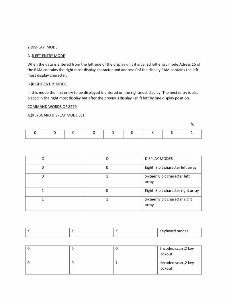
2.DISPLAY MODE
A .)LEFT ENTRY MODE
When the data is entered from the left side of the display unit it is called left entry mode.Adress 15 of
the RAM contains the right most display character and address 0of the display RAM contains the left
most display character.
B.)RIGHT ENTRY MODE
In this mode the first entry to be displayed is entered on the rightmost display. The next entry is also
placed in the right most display but after the previous display i shift left by one display position.
COMMAND WORDS OF 8279
A.)KEYBOARD DISPLAY MODE SET
A0
0 0 0 D D K K K 1
D D DISPLAY MODES
0 0 Eight 8 bit character left array
0 1 Sixteen 8 bit character left
array
1 0 Eight 8 bit character right array
1 1 Sixteen 8 bit character right
array
K K K Keyboard modes
0 0 0 Encoded scan ,2 key
lockout
0 0 1 decoded scan ,2 key
lockout
0 1 0 Encoded scan ,N key
rollover
0 1 1 decoded scan ,N key
rollover
1 0 0 Encoded scan sensor
matrix
1 0 1 decoded scan sensor
matrix
1 1 0 Strobbed input
encoded scan
1 1 1 Strobbed input
decoded scan
B.)PROGRAMMABLE CLOCK
Clock for operation is obtained by dividing the external clock input signal by programmable constant
called prescaler
D7 D6 D5 D4 D3 D2 D1 D1 A0
0 0 1 P P P P P 1
C.)READ FIFO/SENSOR RAM
D7 D6 D5 D4 D3 D2 D1 D1 A0
0 1 0 AI X A A A 1
X- Don’t care
AL—auto increment
AAA—address pointer to 8 bit FIFO ram
D.)READ DISPLAY RAM
D7 D6 D5 D4 D3 D2 D1 D1 A0
0 1 1 AI A A A A 1
IF AI=1 the address is automatically incremented and read operation is performed
E.) WRITE DISPLAY RAM
D7 D6 D5 D4 D3 D2 D1 D1 A0
1 0 0 AI A A A A 1
IF AI=1 the address is automatically incremented and write operation is performed
F.)DISPLAY WRITE INHIBIT / BLANKING
D7 D6 D5 D4 D3 D2 D1 D1 A0
1 0 1 X IW IW BL BL 1
-it is used to mask individual nibbles
G.)CLEAR DISPLAY RAM
D7 D6 D5 D4 D3 D2 D1 D1 A0
1 1 0 CD2 CD1 CD0 CF CA 1
CD2 must be 1 for enabling clear display command
If CF=1 then FIFO is cleared. CA =1 combines the effect of CD and CF
H.)END INTERRUPT / ERROR MODE SET
D7 D6 D5 D4 D3 D2 D1 D1 A0
1 1 1 E X X X X 1
For N-KEY ROLLOVER MODE ,if E bit is set to be 1,8279 operates in special error mode.
KEY CODE AND STATUS DATA FORMAT
A.)KEY –CODE DATA FORMAT
The key code is entered as a byte code into the FIFO RAM after a valid key closure in the
following in the scanned keyboard mode.
CNTL SHIFT D5 D4 D3 D2 D1 D0
D0,D1 ,D2 –Contents of column counter to determine column of key pressed.
D3, D4 ,D5 –Contents of row counter to determine row of key pressed.
The data from the return lines is directly entered into an appropriate row of sensor RAM that identifies
the row of sensor that changed its status in sensor matrix mode.
RL7 RL6 RL5 RL4 RL3 RL2 RL1 RL0
B.)FIFO STATUS WORD
It is used in keyboard and strobbed input mode to indicate error. If FIFO is full and write is attempted
then overrun error occurs .If FIFO is empty and read is attempted then underrun error occurs.
D7 D6 D5 D4 D3 D2 D1 D0
Du S/E O U F N N N
Du-display RAM unavailable due to clearing operation
S/E-sensor closure or error flag for multiple closures
O-overrun error, if O=1
U-underrun error if U=1
FIFO full If F=1
D0, D1, D2—number of character that are available for reading from FIFO
INTERFACING WITH 8086
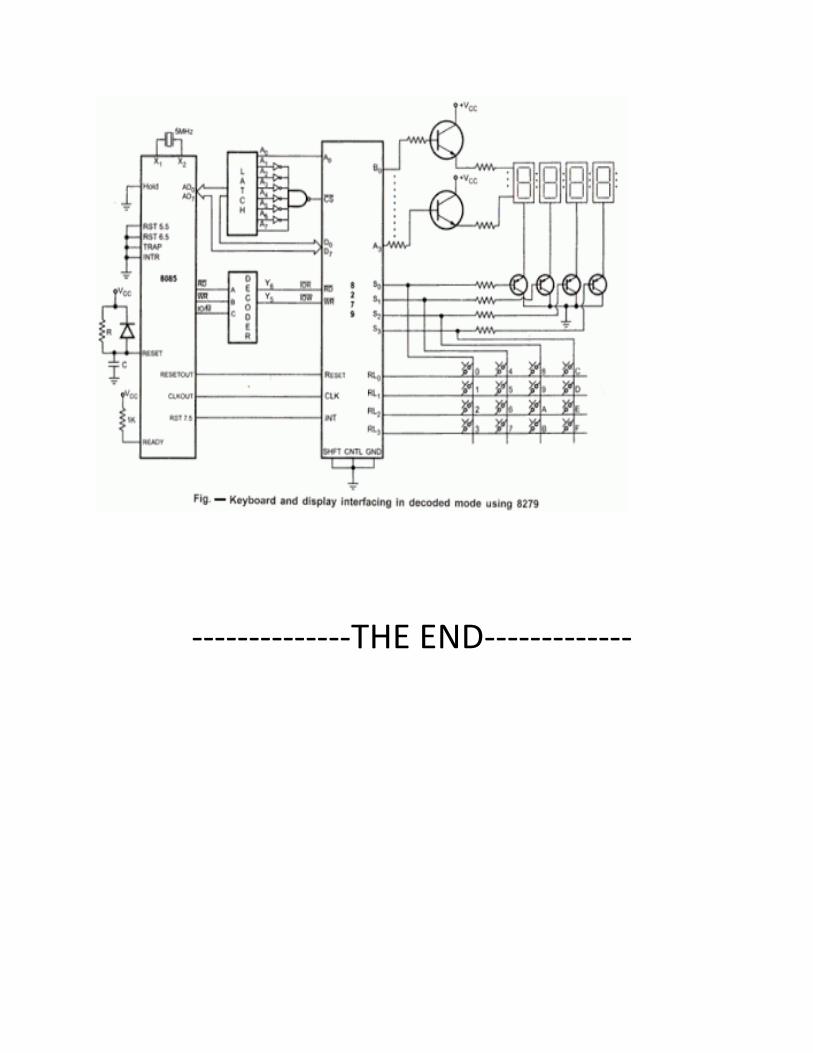
--------------THE END-------------

![ARM9TDMI - atarm.com · This document is a reference manual for the ARM9TDMI microprocessor. ... • a concise explanation of your comments. ... opcode[27:25] = 0b011 and opcode ...](https://static.fdocuments.us/doc/165x107/5b35c6e27f8b9a6b548d913d/arm9tdmi-atarm-this-document-is-a-reference-manual-for-the-arm9tdmi-microprocessor.jpg)