Moulded Interconnect Devices - Loughborough University€¦ · Moulded Interconnect devices ......
34
Prime Faraday Technology Watch ISBN 1-84402-021-5 Moulded Interconnect Devices February 2002 Moulded Interconnect Devices Moulded Interconnect devices (MIDs) can be defined as an injection moulded thermoplastic substrate which incorporates a conductive circuit pattern, and integrates mechanical and electrical functions. They are usually three- dimensional and a variety of techniques may be used to apply the conductors and components. The technology has made significant advances in recent years, particularly the development of light-temperature resins and using rapid prototyping techniques to generate pre-production examples, but requirements for multilayers, high component densities and plated-through holes will continue to be met by conventional planar printed circuit board technology. This overview looks at moulding techniques, metallization, the use of photoresists and adhesives, soldering, device attachment methods including surface mounting and ball grid arrays, prototyping, inspection, testing and reliability, as well as commercial applications, market trends and the environmental aspects of recycling. Andrew Housden and John Gould Pera Knowledge PRIME Faraday Partnership
Transcript of Moulded Interconnect Devices - Loughborough University€¦ · Moulded Interconnect devices ......
Prime Faraday Technology Watch
ISBN 1-84402-021-5 Moulded Interconnect Devices February 2002
Moulded Interconnect Devices
Moulded Interconnect devices (MIDs) can be defined as an injection moulded thermoplastic substrate which incorporates a conductive circuit pattern, and integrates mechanical and electrical functions. They are usually three-dimensional and a variety of techniques may be used to apply the conductors and components. The technology has made significant advances in recent years, particularly the development of light-temperature resins and using rapid prototyping techniques to generate pre-production examples, but requirements for multilayers, high component densities and plated-through holes will continue to be met by conventional planar printed circuit board technology. This overview looks at moulding techniques, metallization, the use of photoresists and adhesives, soldering, device attachment methods including surface mounting and ball grid arrays, prototyping, inspection, testing and reliability, as well as commercial applications, market trends and the environmental aspects of recycling.
Andrew Housden and John Gould Pera Knowledge
PRIME Faraday Partnership
This title is for sale in paperback at Amazon.co.uk http://www.amazon.co.uk/exec/obidos/ASIN/1844020215
Technology Watch titles are written for managers, especially in small and medium-sized manufacturing companies. They offer a practical introduction to cutting-edge developments that affect – or likely soon will affect – the design, development, manufacture and marketing of PRIME products – products with interdependent mechanical and electronic (and possibly software) parts.
All Technology Watch titles can be downloaded free of charge from the Prime Faraday Partnership’s Technology Watch website http://www.primetechnologywatch.org.uk/. Selected titles can be purchased in paperback from Amazon.co.uk.
In addition to market and technology reviews, the Technology Watch website also provides news cuttings, case studies, an events diary and details of funding opportunities. The service is sponsored by the DTI and managed by the PRIME Faraday Partnership, which marries the academic strengths of Loughborough University and the University of Nottingham to the technology-transfer expertise of Pera.
Moulded Interconnect Devices
Prime Faraday Technology Watch – February 2002
Published in 2002 by PRIME Faraday Partnership
Wolfson School of Mechanical and Manufacturing Engineering
Loughborough University, Loughborough, Leics LE11 3TU http://www.primetechnologywatch.org.uk
© 2002 Pera Knowledge
ISBN 1-84402-021-5
Whilst the advice and information in this publication is believed to be true and accurate at the time of publication, neither the author nor the publisher assume any legal responsibility or liability for any error or
omission that may have been made.
Comments on this publication are welcomed. Please send them to <[email protected]>
Moulded Interconnect Devices
Prime Faraday Technology Watch – February 2002 iii
Contents
1.0 Introduction.........................................................................................................1 2.0 Manufacture of Moulded Interconnect Devices ...................................................3
2.1 Moulding and Film Manufacturing Techniques ................................................4 2.1.1 Single-Shot Injection Moulding and Photoimaging.........................................4 2.1.2 Two-Shot Moulding ..................................................................................5 2.1.3 Film Techniques.......................................................................................6
2.2 Materials .........................................................................................................8 2.3 Types of Conductors.....................................................................................10
3.0 Applications and Markets..................................................................................12 3.1 MID Applications ...........................................................................................12
3.1.1 Antennas................................................................................................13 3.1.2 Automotive Areas...................................................................................13 3.1.3 Computer Joysticks................................................................................14 3.1.4 Television Manufacture..........................................................................14
3.2 Market Development.....................................................................................15 4.0 Design Processes for Three-Dimensional Moulded Interconnects ....................17
4.1 Circuit Design ....................................................................................................18 4.2 Prototyping....................................................................................................19 4.3 Production.....................................................................................................20
5.0 Soldering, Adhesives and Assembly Issues......................................................23 5.1 Soldering.......................................................................................................23 5.2 The Role of Adhesives in Moulded Interconnect Devices..............................24 5.3 Recycling of MIDs .........................................................................................25
6.0 Conclusions......................................................................................................27 7.0 Sources of Information......................................................................................29 8.0 References.......................................................................................................30
Tables
Table 1 – Typical MID Substrate Materials ....................................................................9 Table 2 – Typical Moulded Circuit Conductor Materials...............................................11 Table 3 – Sales of Moulded Interconnect Devices.......................................................15
Figures
Figure 1 - MID Manufacturing Processes ......................................................................3 Figure 2 - The Capture Process ....................................................................................7 Figure 3 - MID Technology integrates mechanical and electrical functions..................12 Figure 4 - MID Interdependencies ...............................................................................19 Figure 5 - Requirement Profiles...................................................................................21 Figure 6 - Process Technologies.................................................................................22
Moulded Interconnect Devices
Prime Faraday Technology Watch – February 2002 1
1.0 Introduction The convergence of resilient thermoplastic materials with techniques such as selective metal coatings is bringing a new dimension to circuit boards: 3-D moulded interconnect devices (3-D MIDs). A moulded interconnect Device (MID) is defined simply as:
"…an injection moulded plastic substrate which incorporates a conductive circuit pattern, and integrates both mechanical and electrical functions.”
Source: MIDIA (Molded Interconnection Device International Association)
Traditional printed circuit boards (PCBs) are two-dimensional constructs that typically accommodate electronic components on either one or both of their sides. 3D MIDs are plastic mouldings that incorporate, or have on their surface, an integrated conductive pattern. As such they represent the fusion of mechanical and electrical functionally into one integrated component. MIDs possess enormous potential for technical innovation and rationalization and are substantially more environmentally friendly than conventional PCBs, which they are intended to supplement but not replace. They are revolutionising traditional mechanical and electrical designs in many applications, particularly in the automotive and telecommunication industries. For electromechanical designers and many other electronics professionals, MIDs can offer significant advantages over design approaches based on traditional PCBs. The essential benefits of MIDs arise from their proven capability to integrate mechanical and electrical functions into a single component. If a product consists of a simple circuit board and protective housing, MID technology is unlikely to prove an attractive or cost-effective option. However, for products with some degree of electromechanical complexity, such as a mobile telephone with a flip or slide open action, MID is a viable option. With PCBs limited to planar applications, MIDs often utilise three-dimensional circuitry; a circuit pattern with several planes allows better circuitry spacing, as well as the potential for integrated switches, connectors and buttons. MIDs can also reduce the number of components and cost by embedding features such as connectors, wire harnesses or lamp-holders within a single device. In addition they can be designed to be self-supporting thus eliminating any requirement for mechanical parts needed to support the circuit boards. Through reducing part numbers, MIDs save space and shorten assembly time.

Moulded Interconnect Devices
Prime Faraday Technology Watch – February 2002 2
The major limitation of MIDs is their relatively low circuit density. MID technology cannot replace the layered or hidden circuitry in traditional boards, and unlike mutilayer PCBs, which can have 16, 24 or 32 layers, MIDs typically only have two layers, the front and back of the part. Designing moulded interconnect devices therefore requires a new approach. It demands that the designer think in terms of three dimensions. Using this technology, more efficient and lower-cost designs are possible, making the process very attractive.
Moulded Interconnect Devices
Prime Faraday Technology Watch – February 2002 3
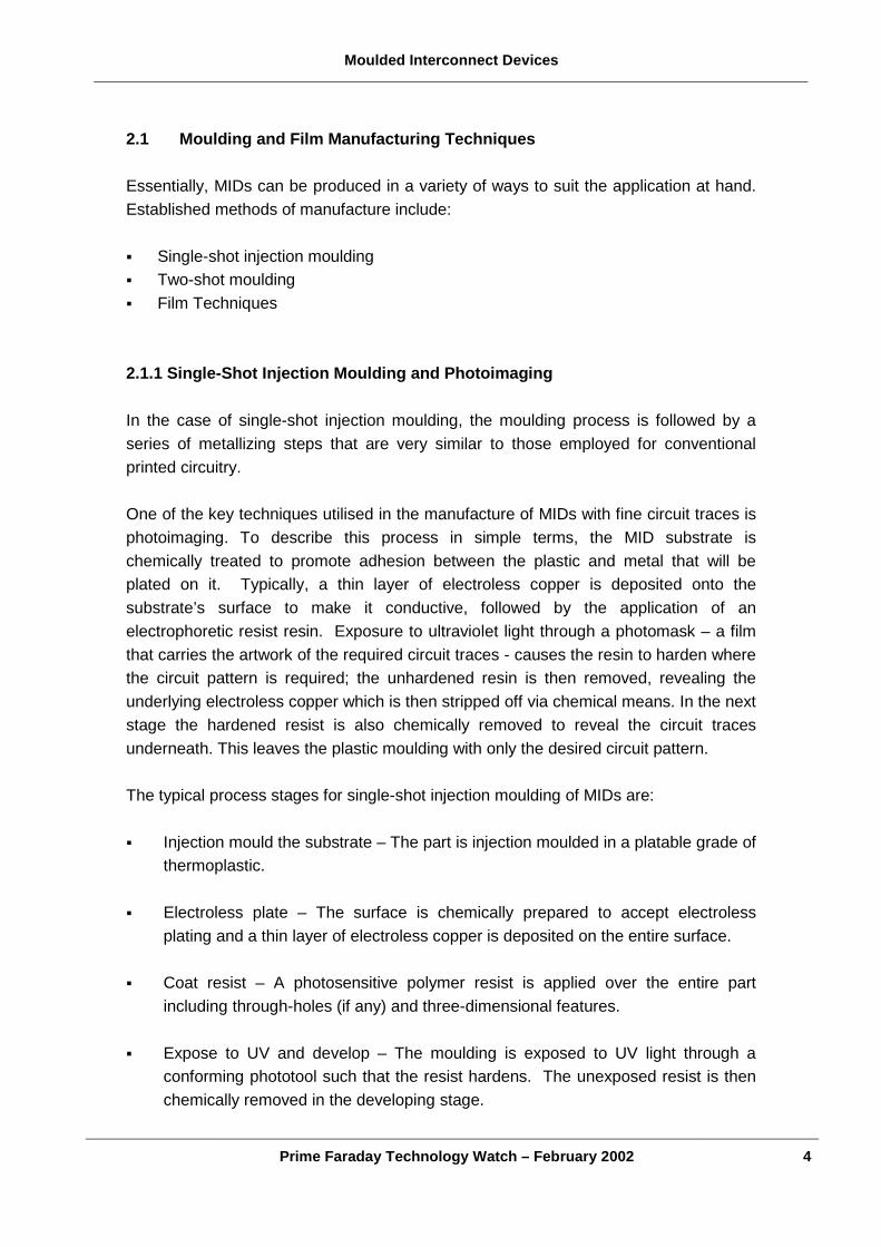
2.0 Manufacture of Moulded Interconnect Devices Some of the essential manufacturing processes and materials associated with the production of MIDs differ significantly from those employed to produce conventional PCBs. In conventional PCB manufacture, with its fine dimensional tolerances and low margins of error, product design is principally centred on the optimum placement of electronic components onto the selected substrate material, via a bonding process such as soldering. In this process the properties, dimensions and performance of the selected substrate are well known and account can be taken of these characteristics. In the production of MIDs, the substrate material selected is closely related to, or indeed is, the final component. As such the behaviour and performance of the material is often subject to a significant number of additional functional and design requirements. Figure 1 highlights some of the typical MID manufacturing processes.
Figure 1 - MID Manufacturing Processes
Source: Built-in Integration - Siemens R&D Archive 1997 - Frank Pöhlau.
Moulded Interconnect Devices
Prime Faraday Technology Watch – February 2002 4
2.1 Moulding and Film Manufacturing Techniques Essentially, MIDs can be produced in a variety of ways to suit the application at hand. Established methods of manufacture include: � Single-shot injection moulding � Two-shot moulding � Film Techniques 2.1.1 Single-Shot Injection Moulding and Photoimaging In the case of single-shot injection moulding, the moulding process is followed by a series of metallizing steps that are very similar to those employed for conventional printed circuitry. One of the key techniques utilised in the manufacture of MIDs with fine circuit traces is photoimaging. To describe this process in simple terms, the MID substrate is chemically treated to promote adhesion between the plastic and metal that will be plated on it. Typically, a thin layer of electroless copper is deposited onto the substrate’s surface to make it conductive, followed by the application of an electrophoretic resist resin. Exposure to ultraviolet light through a photomask – a film that carries the artwork of the required circuit traces - causes the resin to harden where the circuit pattern is required; the unhardened resin is then removed, revealing the underlying electroless copper which is then stripped off via chemical means. In the next stage the hardened resist is also chemically removed to reveal the circuit traces underneath. This leaves the plastic moulding with only the desired circuit pattern. The typical process stages for single-shot injection moulding of MIDs are: � Injection mould the substrate – The part is injection moulded in a platable grade of
thermoplastic. � Electroless plate – The surface is chemically prepared to accept electroless
plating and a thin layer of electroless copper is deposited on the entire surface. � Coat resist – A photosensitive polymer resist is applied over the entire part
including through-holes (if any) and three-dimensional features. � Expose to UV and develop – The moulding is exposed to UV light through a
conforming phototool such that the resist hardens. The unexposed resist is then chemically removed in the developing stage.
Moulded Interconnect Devices
Prime Faraday Technology Watch – February 2002 5
� Electroplate metals – Copper and metals such as tin/lead or nickel/gold are deposited.
� Strip resist and etch background copper – The resist is removed from unplated
areas and the background copper is etched. There is a variation of this process which utilises fully additive plating techniques. In this case the entire plastic substrate is copper plated to a specified final thickness before resist is applied. The photomask is designed so that this resist is exposed and hardened only where the circuit tracks are required. After unhardened resist is chemically removed, the entire thickness of copper which has been uncovered is removed, again leaving the plastic substrate with only the desired circuit pattern. However, the copper tracks are still covered with hardened resist, which is then chemically removed so that the circuitry can be finished as required. 2.1.2 Two-Shot Moulding This uses two separate moulding cycles and usually different polymers to form the component. It requires the construction of different mould cavities for each shot. Catalysed resin versions of this process use a polymer that contains a small quantity of plating catalyst. The part is designed so that imaging is undertaken during moulding by leaving this catalysed resin exposed on the surface of the final part only where the circuit traces are required. This is accomplished by creating two moulds. The first shot is moulded and then inserted into the second mould in which the second resin system forms the final three-dimensional features of the component. Depending on part design, either the first or second shot resin may be the one containing a plating catalyst. Chemical treatment is undertaken to promote adhesion between the plastic and the metal plated onto it so that when the moulding is put through an electroless copper plating cycle, only resin containing the catalyst plates and thus creates the circuit pattern. Other electroless metal overlays can be applied if desired, and it is not unusual to employ rotary moulds or robotic handling for two-shot moulding processes. The process stages therefore are: � Injection mould first shot – A first shot, which usually contains non-catalysed resin,
is injection moulded in one cavity in a mould. This produces a first-stage moulding having identifiable areas for placement or incorporation of further moulding material for additional processing.
Moulded Interconnect Devices
Prime Faraday Technology Watch – February 2002 6
� Injection mould second shot – The first-stage moulding is inserted into a second cavity where a second shot, generally of platable catalysed resin, is introduced into the mould. This typically produces a moulding with exposed, platable, catalysed resin on its surface, the patterns of which define the required circuit tracks.
� Promote adhesion – As part of the plating process, the moulding undergoes a
chemical treatment to enhance the ability of catalysed resin to accept plating. � Plate the part – The moulding is copper plated to a specified thickness. Metallic
or organic finishes may then be applied. A variation of this technique is to use resins which do not contain a plating catalyst. In this case the first shot is moulded and chemically treated with a catalyst before moulding the second shot. Copper plating is then undertaken and only the resin that has been chemically treated plates to form circuits. So, two-shot moulding can enable very complex three-dimensional circuitry to be produced, limited only by an ability to mould the component since there are no additional imaging steps involved. Plated-through holes can be accommodated, but because circuit design changes usually require mould modifications it is more difficult and expensive to incorporate changes on parts within this process. Line and width spacing is limited by the moulding process, and it is generally difficult to achieve spacings as low as other PCB techniques; a typical value is 0.25mm. It is the least labour-intensive process and generally the easiest to automate for high-volume production. However, tooling costs are high, which means that it is more suited to high-volume production requirements, typically associated with the telecommunications and automotive industries. 2.1.3 Film Techniques Processes under this heading have in common the fact that the conducting material starts out as a separate flexible film and is subsequently attached to an injection-moulded plastic substrate. The conductors are usually formed from copper laminate, foil or silver conductive inks on a carrier. Typical film processes are: � Capture Process � Transfer Process � Hot Stamping
Moulded Interconnect Devices
Prime Faraday Technology Watch – February 2002 7
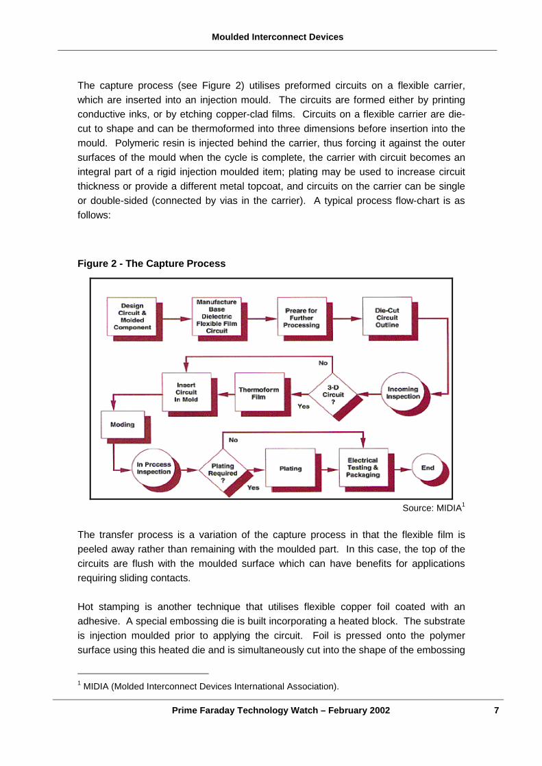
The capture process (see Figure 2) utilises preformed circuits on a flexible carrier, which are inserted into an injection mould. The circuits are formed either by printing conductive inks, or by etching copper-clad films. Circuits on a flexible carrier are die-cut to shape and can be thermoformed into three dimensions before insertion into the mould. Polymeric resin is injected behind the carrier, thus forcing it against the outer surfaces of the mould when the cycle is complete, the carrier with circuit becomes an integral part of a rigid injection moulded item; plating may be used to increase circuit thickness or provide a different metal topcoat, and circuits on the carrier can be single or double-sided (connected by vias in the carrier). A typical process flow-chart is as follows:
Figure 2 - The Capture Process
Source: MIDIA1
The transfer process is a variation of the capture process in that the flexible film is peeled away rather than remaining with the moulded part. In this case, the top of the circuits are flush with the moulded surface which can have benefits for applications requiring sliding contacts. Hot stamping is another technique that utilises flexible copper foil coated with an adhesive. A special embossing die is built incorporating a heated block. The substrate is injection moulded prior to applying the circuit. Foil is pressed onto the polymer surface using this heated die and is simultaneously cut into the shape of the embossing
1 MIDIA (Molded Interconnect Devices International Association).
Moulded Interconnect Devices
Prime Faraday Technology Watch – February 2002 8
die, thus forming a circuit. It is a relatively simple technique but the plastic surface where the circuit is to be embossed must be comparatively flat or have a smooth, uniform contour so that the embossing die can precisely contact the surface. The activities of German company Krauss-Maffei, a plastic machinery manufacturer, point the way to more integrated MID production systems.2 The company have developed machinery which incorporates MID moulding and stamping in a single environment, with the part being moulded and then partially released from the mould and orientated for a stamping operation. The combined process removes the need to pre-heat the moulded part prior to a separate stamping operation. It is said to provide significant energy, time and cost savings over current MID production techniques. In general, these film processes are more easily applied to relatively flat surfaces but are capable of providing moderately complex three-dimensional circuits using special techniques. Since the circuitry is on a separate carrier it is easy to modify circuit design provided this does not necessitate mould modifications. Track line and width spacing in the region of 0.025mm is no real problem, but is it difficult to provide plated through holes. 2.2 Materials Polymers employed in the production of moulded interconnect devices vary depending on the manufacturer or supplier. Some important parameters that must be considered in choosing a material are: � Minimum and maximum usage and assembly temperatures � Requirements for flammability rating � Creep properties � Tensile properties � Flexural properties � Cost � Metallization capability � Moulding characteristics � Electrical properties � Environmental concerns Given the diverse application requirements and environments for MIDs there are many substrate materials that are employed in their manufacture. Table 1 highlights a number of typical MID substrate materials.
2 MIDs Straight from the Mould. www.modplas.com. February 2000.
Moulded Interconnect Devices
Prime Faraday Technology Watch – February 2002 9
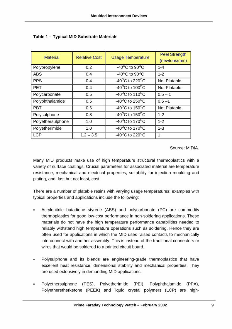
Table 1 – Typical MID Substrate Materials
Material Relative Cost Usage Temperature Peel Strength (newtons/mm)
Polypropylene 0.2 -40OC to 90OC 1-4 ABS 0.4 -40OC to 90OC 1-2 PPS 0.4 -40OC to 220OC Not Platable PET 0.4 -40OC to 100OC Not Platable Polycarbonate 0.5 -40OC to 110OC 0.5 – 1 Polyphthalamide 0.5 -40OC to 250OC 0.5 –1 PBT 0.6 -40OC to 150OC Not Platable Polysulphone 0.8 -40OC to 150OC 1-2 Polyethersulphone 1.0 -40OC to 170OC 1-2 Polyetherimide 1.0 -40OC to 170OC 1-3 LCP 1.2 – 3.5 -40OC to 220OC 1
Source: MIDIA. Many MID products make use of high temperature structural thermoplastics with a variety of surface coatings. Crucial parameters for associated material are temperature resistance, mechanical and electrical properties, suitability for injection moulding and plating, and, last but not least, cost. There are a number of platable resins with varying usage temperatures; examples with typical properties and applications include the following: � Acrylonitrile butadiene styrene (ABS) and polycarbonate (PC) are commodity
thermoplastics for good low-cost performance in non-soldering applications. These materials do not have the high temperature performance capabilities needed to reliably withstand high temperature operations such as soldering. Hence they are often used for applications in which the MID uses raised contacts to mechanically interconnect with another assembly. This is instead of the traditional connectors or wires that would be soldered to a printed circuit board.
� Polysulphone and its blends are engineering-grade thermoplastics that have
excellent heat resistance, dimensional stability and mechanical properties. They are used extensively in demanding MID applications.
� Polyethersulphone (PES), Polyetherimide (PEI), Polyphthalamide (PPA),
Polyetheretherketone (PEEK) and liquid crystal polymers (LCP) are high-
Moulded Interconnect Devices
Prime Faraday Technology Watch – February 2002 10
temperature thermoplastics for products that will encounter high heat or soldering operations. These materials may also be used where precision moulding is necessary.
Resins with wide ranges of chemical resistance are also available for use in aggressive industrial environments where the potential for exposure to a variety of chemical contaminants exists. Detailed information covering the chemical and physical properties of all the thermoplastics commonly used in MID applications is readily available from polymer manufacturers and suppliers. Resin characteristics are particularly important in high frequency applications such as antennas. For this there are two considerations; firstly, the ability to mould to virtually any shape allows antenna designers the freedom to create three-dimensional patterns for optimum radiation performance. Secondly, good electrical properties will also influence emission performance; antenna-design resins must also be selected on the basis of their dielectric and loss properties. The selection of the right MID substrate material is often a complex choice, given the required balance between electrical, thermal and mechanical properties and consideration of ease of manufacture and cost. 2.3 Types of Conductors The definition of a moulded interconnect device implies that a conductive pattern be applied to an injection moulded plastic substrate; hence it is important to understand the various conductor options. As with the selection of plastics, a variety of parameters must be considered in choosing an appropriate surface metallization; some of these are: � Current carrying requirements � Cost � Abrasion resistance � Corrosion resistance � Ductility � Appearance � Adhesion to polymeric substrate � Component assembly requirements � Electrical characteristics � Use of possible components The conductor materials normally employed are tabulated below:
Moulded Interconnect Devices
Prime Faraday Technology Watch – February 2002 11
Table 2 – Typical Moulded Circuit Conductor Materials
MATERIAL PRACTICAL THICKNESS
(microns)
PROPERTIES
Electroplated Copper* 125 • High Ductility • Highest conductivity
Electroless Copper* 50 • Very uniform thickness
Electroplated Tin/Lead* 25 • Fast deposition • Can be reflowed • Good ductility • Good conductivity
Electroplated Tin 12 • Decorative finish
Electroplated Nickel /Tin
25 • Good abrasion surface • Good contact surface
Electroless Nickel 12 • Very hard surface • Most corrosion resistant nickel • Uniform thickness
Electroplated Nickel 25 • Very hard surface • Corrosion resistant • Wire-bond capable
Electroplated Gold* 12 • Hard gold can be used for contact surfaces
• Soft gold can be used for wire bonding • Excellent corrosion protection
Electroplated Gold* 2.5 • Can be applied to isolated traces
Immersion Gold* 0.1 • Good for wire bonding
Immersion Tin 2.0 • Can be used as a protective layer • Good solderability
Silver Ink 50 • Can be screen printed • Can be used to create passive
components
Carbon Ink 50 • Can be screen printed • Good for keypads
* Excellent solderability The current carrying capacity of a trace is dependent on the conductor metallization, the conductor thickness, and the conductor width. The same calculations used to determine current carrying capacity for conventional circuitry may be used for Moulded Interconnect Devices.
Source: MIDIA
Moulded Interconnect Devices
Prime Faraday Technology Watch – February 2002 12
3.0 Applications and Markets 3.1 MID Applications Moulded interconnect devices possess enormous potential for technical innovation and are more environmentally friendly than conventional printed circuit boards, which they are intended to supplement but not replace. Areas of applications for MIDs include automotive electronics, telecommunications, computers, domestic appliances and medical equipment. From a product perspective, MIDs are utilised in applications ranging from cars to airplanes, joysticks to cell phones, and flashlights to antennas.
Figure 3 - MID Technology integrates mechanical and electrical functions
Source: Built-in Integration - Siemens R&D Archive 1997 - Frank Pöhlau. The most important advantages of MID technology when compared with conventional PCBs are in the areas of technology, economics and environment. MIDs can integrate electrical and mechanical elements into almost any shape of interconnect device. They allow new functions to be created and facilitate the miniaturisation of products. The elimination of mechanical components makes assembly easier, speeds up the manufacturing process and improves reliability. In addition, MID technology allows the incorporation of cost-intensive items such as connectors. MIDs also offer environmental benefits in the fact that they use thermoplastic materials with a minimum of additives, which can be recycled easily. Specific benefits include:
Moulded Interconnect Devices
Prime Faraday Technology Watch – February 2002 13
� Reduced number of piece parts � Lower cost � Less assembly time � Higher reliability � Lower weight � Shielding � Smaller sized modules � Complex three-dimensional electromechanical interconnects � Full compatibility with modern manufacturing techniques � Ability to withstand harsh environments � Recycling By enabling a reduction in the numbers of parts, allowing further automation of the assembly process and by effectively miniaturising the size of the component, the application of MIDs often allows for a consequent reduction in assembly costs of 30-40%. Therefore, MID is widely used for electronic devices such as those found in the automotive industry. There are many examples of the application of MID technology, a number of typical examples of their uses follow. 3.1.1 Antennas The telecommunications industry has found advantages in using MIDs for the internal antenna of cellular phones. This type replaces the normal antenna stub or retractor. Using the antenna as part of the phone’s internal fixtures, volume limitation in cell phones is overcome by achieving more efficient use of space. With the increasing popularity of changeable phone covers, MID technology is also being employed to add electrical functionality to such covers for the purposes of miniaturisation and increasing shielding efficiency. MID moulding and plating characteristics can be easily modified to produce attractive and functional colours and shapes. 3.1.2 Automotive Areas An increasing application for MID technology is rear lamp clusters. Traditional fixtures comprise of various parts including a moulded housing, stamped metal inserts, connectors and solder-attached wiring. The MID version combines the connector and
Moulded Interconnect Devices
Prime Faraday Technology Watch – February 2002 14
housing in one piece, and through selective plating it incorporates all the required circuitry. The resulting MID is a single unit that holds the bulbs, non-soldered circuitry and a port that interfaces with the vehicles electrical system. With the numerous lighting fixtures present on cars, the requirements in this sector alone will be very substantial. In general, other automotive applications having stamped metal inserts could potentially benefit from MID design. The automotive area is recognised as an area of intense interest in MID technology.3 3.1.3 Computer Joysticks Computer peripherals such as joysticks are also candidates for MID solutions. The limited space available makes it very difficult to position push-button switches within the joystick for provision of controls similar to those in a flight simulator. Switches are located in different planes, each requiring its own circuit board and connecting wires. The problem can be solved using MID technology by providing electrical pathways and mounting pads over multiple planes in one component. By this means, many separate wires and circuit boards, together with significant labour costs are eliminated. Other limited-space switch applications could benefit from this technology. 3.1.4 Television Manufacture The use of MID technology in the manufacture of television sets is of interest for several reasons. In the first instance, MIDs are manufactured using thermoplastic polymers, which are more easily recycled and can be designed not to contain halogenated flame-retardants. The use of MIDs also considerably reduces the number of assembly steps when compared to PCBs and they also offer a greater level of design freedom. It is reported that the German manufacturer Grundig is heavily involved in the development of MID technologies for manufacturing environmentally friendly (‘green’) television sets. They are expected to use MIDs in the signal processing, control and power modules of the set. It is hoped the whole television thus manufactured will be more environmentally friendly than current models; not only will it be made using environmentally-sound techniques but it will also be more recyclable and cost-effective. 3 3-D interconnect offer sizeable market opportunity. Peter Mapleston. Plastiscope. March (2000).
Moulded Interconnect Devices
Prime Faraday Technology Watch – February 2002 15
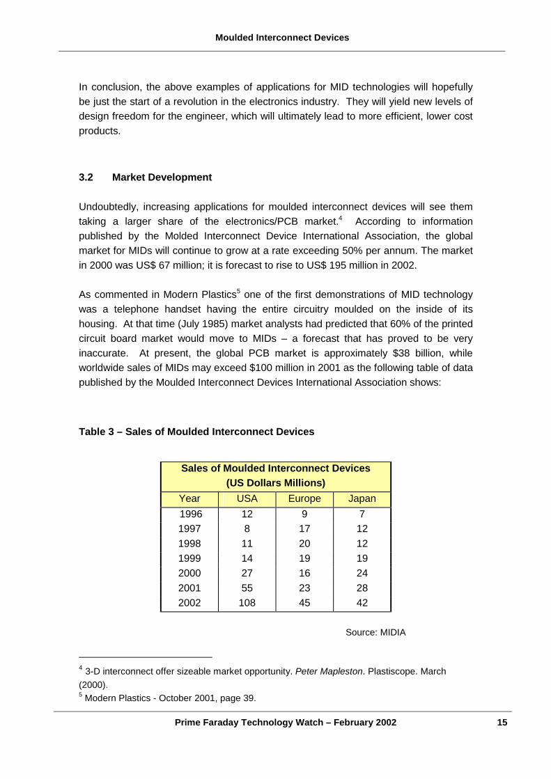
In conclusion, the above examples of applications for MID technologies will hopefully be just the start of a revolution in the electronics industry. They will yield new levels of design freedom for the engineer, which will ultimately lead to more efficient, lower cost products. 3.2 Market Development Undoubtedly, increasing applications for moulded interconnect devices will see them taking a larger share of the electronics/PCB market.4 According to information published by the Molded Interconnect Device International Association, the global market for MIDs will continue to grow at a rate exceeding 50% per annum. The market in 2000 was US$ 67 million; it is forecast to rise to US$ 195 million in 2002. As commented in Modern Plastics5 one of the first demonstrations of MID technology was a telephone handset having the entire circuitry moulded on the inside of its housing. At that time (July 1985) market analysts had predicted that 60% of the printed circuit board market would move to MIDs – a forecast that has proved to be very inaccurate. At present, the global PCB market is approximately $38 billion, while worldwide sales of MIDs may exceed $100 million in 2001 as the following table of data published by the Moulded Interconnect Devices International Association shows:
Table 3 – Sales of Moulded Interconnect Devices
Source: MIDIA
4 3-D interconnect offer sizeable market opportunity. Peter Mapleston. Plastiscope. March (2000). 5 Modern Plastics - October 2001, page 39.
Sales of Moulded Interconnect Devices (US Dollars Millions)
Year USA Europe Japan 1996 12 9 7 1997 8 17 12 1998 11 20 12 1999 14 19 19 2000 27 16 24 2001 55 23 28 2002 108 45 42

Moulded Interconnect Devices
Prime Faraday Technology Watch – February 2002 16
Two of the most significant examples of MID technology are a two-component coaxial connector for mobile phones and a polymer stud grid array (PSGA) that is “smaller than a thumbnail”. W.C. Herans at Harau in Germany is a leading company in plastics/metal technologies for electronics. They suggest that many OEMs are not ready to move vital componentry to a relatively new technology, but for products such as mobile phones the risk is worth taking whereas automotive companies have to offer product warranties in excess of three years and product liability issues are more critical. Herans began production of MID-type coaxial connectors at the beginning of 2001. Their technology employs a two-shot moulding process using two grades of liquid crystal polymer. One contains a palladium catalyst that allows the part to be plated, and two Battenfeld Microsystem 50 presses are coupled by a linear robotic transfer system to move parts from one mould to the next for overmoulding. Part weight is 0.13g and cycle time is less than 7 seconds. These connectors replace a previous design which used one polymeric and four metallic components. The other example of new-generation MID technology is a PSGA from Siemens Dematic. It is a chip carrier particularly suited to mobile phones and portable computers. Metallized studs are an integral part of the moulding and connect devices to a circuit board. Stud spacing is 0.8mm and each stud is 0.4mm wide so they are much stronger and dimensionally stable than solder that is more commonly used on conventional ball grid arrays. Siemens Dematic is licensing the technology and is in pilot production. PSGA chip carriers offer higher termination density and thermal conductivity, better RFI/EMI shielding, substantially greater reliability, and lower cost than conventional technologies. Accordingly the company envisages increased use of PSGAs in automotive electronics, consumer products and telecommunications equipment. Several other market predictions have been made for moulded interconnect devices in the literature.6,7 For example, Professor Klaus Feldmann on the University of Erlangen, Germany, suggests in Kunstsoffe/Plastics Europe8, that the market for MID applications is expected to grow to approximately 1.2 billion DM in 2005 from 83 million DM in 2000, again predominantly in the telecommunications and automotive sensor markets.
6 3D moulded circuits stronger than boards. Eureka transfer technology. October 1995. 7 The European Electronic Components Market 1998-2002 – active Components, Passive Components, Electromechanical Components, Other Components and Modules. Market Tracking International. May (1998). 8 Kunstsoffe/Plastics Europe, November, 2000, p26.
Moulded Interconnect Devices
Prime Faraday Technology Watch – February 2002 17
4.0 Design Processes for Three-Dimensional Moulded Interconnects With the development of powerful workstations and the availability of easy-to-use solid modelling software, the tools for 3-D moulded interconnect design have been available for several years. Although it is possible to begin a conceptual design with 2-D software and progress to 3-D software at a later stage, design of the product from the beginning in a 3-D environment offers numerous advantages. Designing in 3-D minimises the amount of effort needed during conceptual design and builds a database for final design and prototyping. As the product design begins to evolve, major electrical/electronic and mechanical components are selected. The general placement or special location and orientation of major items are determined based on their function and input from other design team members. It is important in this design process to place all the electrical and electromechanical components such as motors, keyboards, displays, control electronics and power supplies. Each component can be positioned in the product, based on its thermal, mechanical and physical requirements so that once the product concept and major component placement exists, the interconnect design strategy can begin. Product cost, thermal management, manufacturability, EMI/RFI/ESD shielding requirements and appearance must be considered when determining physical layout but once it has been decided that it is cost- and performance-effective to use a moulded interconnect structure rather than discrete wires or a wiring harness, the design process continues. There are three basic design options when utilising moulded interconnect structures. The first is to use the base or cover of a product as the substrate for moulded interconnects. This works well if the polymer is compatible with copper plating processes and the planned assembly technology. All electrical components must be surface mounted because connection points by necessity are inside the product shell. This design option could require additional processing steps such as painting for cosmetic reasons, and therefore structural or aesthetic requirements will dictate its viability. The second option is to mould an interconnect structure that would fit into the base or cover. This interconnect can either be the main structural component of a system or an interconnect subassembly that drops into a main support structure inside the covers; most of the structural/interconnect properties will be incorporated into this drop-in subassembly. This method may add slightly to cost, but it does allow a wider selection of materials for the outer covers. Additionally, shielding may be separated from the interconnect and can be located on the inside of the covers.
Moulded Interconnect Devices
Prime Faraday Technology Watch – February 2002 18
The final option is to use an existing component or structure, this involves analysing a product, picking likely candidates and evaluating them for conversion to a moulded interconnect device. It can be used in the cost-reduction of recently-designed products and may be quite useful in that it gives a feel for 3-D interconnects and provides direct cost comparisons. 4.1 Circuit Design Once the basic design option has been determined or, more realistically, a strategy evolves during the development cycle, component orientations and interconnect points can be detailed on the newly-developed solid model. The number of interconnect lines and their approximate paths are estimated to ensure that the interconnect strategy limitations (i.e. circuit trace width, track-to-track width, etc.) are not exceeded. Then, working from solid models of the assembly, a flat structure can be built around the existing electrical and electromechanical components so that when the x-y planes are defined the completed image begins to look like a flexible circuit. The three-dimensional model of this “flex circuit” must be prepared for transfer to printed circuit board design software, a task that is fairly easily achieved using sheet metal modelling techniques. This can be modified as the design progresses so that all non-electrical components clear the structure. Holes and other planar features need to be added to the sheet metal model so that registration points on major interconnection areas are located for both the 3-D solid model and electronic design software. A final stage in the design process is to take the sheet metal model and flatten it. This provides an accurate two-dimensional representation of the interconnect structure with specific component locations that may be passed directly into the circuit design software. Concurrent with this, the solid model can be refined so that bosses, ribs, or other structural elements are added. Hence the design process between mechanical engineering, electrical engineering, electronics and PCB layout is completely iterative, and throughout the design process data needs to be examined from a system perspective via the solid model to ensure that the interconnect structure continues to fit within the product concept and will perform to requirements set by electrical, mechanical and PCB dictates. The challenge for the designer is to match the requirements of a given application with the abilities of available materials and process chains, due consideration being given to their economics. Despite a relatively large amount of available data these interdependencies are often unclear but are illustrated in Figure 4.
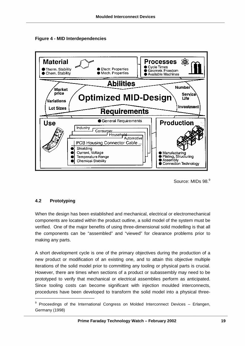
Moulded Interconnect Devices
Prime Faraday Technology Watch – February 2002 19
Figure 4 - MID Interdependencies
Source: MIDs 98.9
4.2 Prototyping When the design has been established and mechanical, electrical or electromechanical components are located within the product outline, a solid model of the system must be verified. One of the major benefits of using three-dimensional solid modelling is that all the components can be “assembled” and “viewed” for clearance problems prior to making any parts. A short development cycle is one of the primary objectives during the production of a new product or modification of an existing one, and to attain this objective multiple iterations of the solid model prior to committing any tooling or physical parts is crucial. However, there are times when sections of a product or subassembly may need to be prototyped to verify that mechanical or electrical assemblies perform as anticipated. Since tooling costs can become significant with injection moulded interconnects, procedures have been developed to transform the solid model into a physical three- 9 Proceedings of the International Congress on Molded Interconnect Devices – Erlangen, Germany (1998)
Moulded Interconnect Devices
Prime Faraday Technology Watch – February 2002 20
dimensional component. These involve two distinctly different technologies that relate back to the solid model of the interconnect and the electrical circuit design. The first step of the prototyping process is to produce a physical structural interconnect shape using stereolithography. This utilises the solid model database and laser equipment to polymerise a special liquid such that three-dimensional shape is grown. Then flexible circuit technology is used to provide a means of electrical connection and circuit verification. The key to prototyping is to bond a functional flex circuit onto a stereolithography model. However, the mechanical integrity of stereolithography models tends to be fairly low and therefore the prototype should only be used to convey the design concept, check the fit with other assemblies and demonstrate the assembly technology. Components can be assembled onto this structure using conductive adhesives or by soldering, and depending on the types of component used, the flex circuit may be assembled in flat form (surface mount) or assembled after bonding to the stereolithography model (through hole). This prototype is then assembled into other prototype components that make the product to check all aspects of the interconnection scheme and its integration into the product. 4.3 Production An ability to manufacture moulded interconnect devices at low cost with high reliability is a primary key to success or failure. The challenge of using MID technology is to have sufficient knowledge of the manufacturing process available to design engineers, so ensuring that once the product is designed it will be easily made. Manufacturing issues range from the types of component that are available to top-down assembly of the final covers. For instance, if the interconnected structure has components soldered using surface mount or through-hole technology, it is critical that the assembly process meets two requirements: � Injection moulded interconnect materials must be able to withstand the assembly
process for component attachment. � The manufacturing department or assembly contractor must have, or plan to
purchase, equipment that automatically assembles the components. It is not considered advisable to design an interconnect structure that will cost less to build than individual harnesses and cables if the electrical components need to be hand assembled. Adding features to hold large and difficult-to-handle electronics will significantly reduce assembly costs; for example break-away panel features and supports for existing assembly equipment can be added for integration into many standard manufacturing processes. Also, once a moulded interconnect has been
Moulded Interconnect Devices
Prime Faraday Technology Watch – February 2002 21
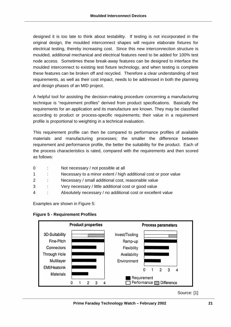
designed it is too late to think about testability. If testing is not incorporated in the original design, the moulded interconnect shapes will require elaborate fixtures for electrical testing, thereby increasing cost. Since this new interconnection structure is moulded, additional mechanical and electrical features need to be added for 100% test node access. Sometimes these break-away features can be designed to interface the moulded interconnect to existing test fixture technology, and when testing is complete these features can be broken off and recycled. Therefore a clear understanding of test requirements, as well as their cost impact, needs to be addressed in both the planning and design phases of an MID project. A helpful tool for assisting the decision-making procedure concerning a manufacturing technique is “requirement profiles” derived from product specifications. Basically the requirements for an application and its manufacture are known. They may be classified according to product or process-specific requirements; their value in a requirement profile is proportional to weighting in a technical evaluation. This requirement profile can then be compared to performance profiles of available materials and manufacturing processes; the smaller the difference between requirement and performance profile, the better the suitability for the product. Each of the process characteristics is rated, compared with the requirements and then scored as follows: 0 : Not necessary / not possible at all 1 : Necessary to a minor extent / high additional cost or poor value 2 : Necessary / small additional cost, reasonable value 3 : Very necessary / little additional cost or good value 4 : Absolutely necessary / no additional cost or excellent value Examples are shown in Figure 5:
Figure 5 - Requirement Profiles
Source: [1]
Moulded Interconnect Devices
Prime Faraday Technology Watch – February 2002 22
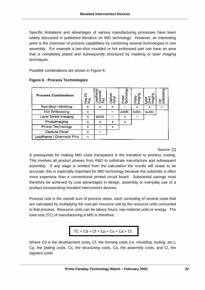
Specific limitations and advantages of various manufacturing processes have been widely discussed in published literature on MID technology. However, an interesting point is the extension of process capabilities by combining several technologies in one assembly. For example a two-shot moulded or hot embossed part can have an area that is completely plated and subsequently structured by masking or laser imaging techniques. Possible combinations are shown in Figure 6.
Figure 6 - Process Technologies
Source: [1]
A prerequisite for making MID costs transparent is the transition to process costing. This involves all product phases from R&D to substrate manufacture and subsequent assembly. If any stage is omitted from the calculation the results will cease to be accurate; this is especially important for MID technology because the substrate is often more expensive than a conventional printed circuit board. Substantial savings must therefore be achieved by cost advantages in design, assembly or everyday use of a product incorporating moulded interconnect devices. Process cost is the overall sum of process steps, each consisting of several costs that are calculated by multiplying the cost per resource unit by the resource units consumed in that process. Resource units can be labour hours, raw material units or energy. The total cost (TC) of manufacturing a MID is therefore:
TC = Cd + Cf + Cp + Cs + Ca + Cl Where Cd is the development costs, Cf, the forming costs (i.e. moulding, tooling, etc.), Cp, the plating costs, Cs, the structuring costs, Ca, the assembly costs, and Cl, the logistics costs
Moulded Interconnect Devices
Prime Faraday Technology Watch – February 2002 23
5.0 Soldering, Adhesives and Assembly Issues 5.1 Soldering One obstacle to the introduction of moulded interconnect devices into mass production has been a lack of knowledge about the thermal limits and solderability of engineering thermoplastics. In general, the high thermal stresses developed during soldering has meant that expensive high-temperature thermoplastics have had to be used for producing MIDs. For this reason the use of engineering plastics offers economic advantages as well as a potential for further processing and recycling. The maximum temperature limit of polymers is determined by heat deflection in addition to physical or chemical ageing. Also, the thermal expansion of most polymers is significantly greater than most metals, which may cause conductor detachment if excessive heat input occurs during a soldering operation. Heat deflection temperature specifies the softening point of polymers subjected to a static load. Experimental measurements are defined in various standards, including ISO75, but in general they require that test specimens be heated in a controlled manner under a defined load. The temperature at which deformation reaches a defined criterion is known as the heat deflection temperature. Physical ageing does not influence the chemical structure of polymers, but their morphology is affected by subsequent recrystallization or relaxation processes. These changes can cause shrinkage or warping that may result in the development of cracks. Additionally, molecules and fillers become oriented during polymer processing. The relaxation of this orientation occurs at temperatures above the glass transition point and is always associated with distortion. Polymers also chemically degrade in the presence of oxygen, a process that is accelerated by heat, water and the presence of catalytic agents. Moulded interconnect devices are in service for a number of years and must therefore not undergo any significant degradation in chemical, physical, mechanical or aesthetic properties, so to inhibit oxidative degradation many thermoplastic polymers have stabiliser systems added to them. When electronic components are soldered, the necessary heat can act in different ways. For example, in wave and reflow soldering the whole surface of the MID exposed to the heat source sees a high temperature whereas the energy in selective soldering processes is only applied in the vicinity of component connections. So, from a thermal viewpoint, soldering in electronic engineering must accommodate two opposing demands; a sufficiently high temperature must be guaranteed in order to

Moulded Interconnect Devices
Prime Faraday Technology Watch – February 2002 24
achieve good wetting by the solder, but thermal stresses should not mechanically or functionally damage components or substrates. Peak surface temperatures vary according to the soldering process. They can be as high as 400oC for short-duration (100ms) laser soldering, or up to 260oC for wave soldering (10s) and reflow soldering (30s). In the latter two cases this peak temperature is reached after through heating at 150oC for 4-6 minutes. With infrared reflow soldering an MID is heated using a predetermined temperature profile and the heat is applied via radiation and convection. Wave soldering is more demanding than infrared reflow soldering because heat transmission is by convection and conduction; as a result, temperature gradients can arise that lead to distortion. Lasers offer a significant number of advantages over conventional soldering techniques because pulsed Nd:YAG laser systems are able to generate very localised, short-duration heat with minimal risk of substrate damage provided appropriate sensors are incorporated. Laser soldering is particularly useful for attaching surface mount devices. Two methods can be applied. The first involves sequential soldering of each lead to its circuit pad, but requires that the component be held in position so that neighbouring leads do not act as spacers and prevent full immersion of the joint being soldered. Alternatively, it is possible to simultaneously apply laser energy to all the solder pad/lead interfaces, when a hold-down arrangement is not essential although the use of such a device is desirable because it will improve thermal contact in the joints. Careful control of laser energy is necessary so that the joint is initially warmed before melting of the solder occurs. Excessive heat input will almost certainly damage the substrate, but partial melting can sometimes be tolerated if it does not significantly degrade circuit performance. However, excessive heating may lead to substrate carbonisation with a consequent risk of insulation loss. Most laser soldering systems are based on pulsed Nd-YAG devices and therefore it is necessary to establish a relationship between pulse duration and laser power to ensure that adequate solder wetting is achieved without substrate damage. This entails the application of a control mechanism that is frequently based on pyrometry, so while laser soldering of single joints is comparatively easy there can be many problems with simultaneous soldering as in device attachment. 5.2 The Role of Adhesives in Moulded Interconnect Devices As discussed, a MID consists of a polymeric body or housing that is provided with a conductor pattern onto which electrical components are mounted. The most widely used plastics for the body are high temperature resistant thermoplastics such as:
Moulded Interconnect Devices
Prime Faraday Technology Watch – February 2002 25
� Polyetherimide (PEI) � Liquid crystal polymers (LCPs) � Polyphthalamides (PPAs) � Thermoplastic polyesters (e.g. PBT, polybutylene terephthalate) � Special polyamides (nylons) In general, the higher temperature plastics are more expensive. For some applications (e.g. housings for telecommunications), lower temperature thermoplastics such as acrylonitrile butadiene styrene (ABS) are commonly used and soldering techniques cannot be employed, as the plastic may unacceptably soften. Wherever substrates or components require lower process temperatures, adhesive bonding is one of the favoured interconnection technologies. With the trend to lead-free materials, an increasing use of adhesives for interconnection purposes can be anticipated, even where soldering could be used. In context, adhesive assembly is not a general alternative to soldering but it is a possible solution for many niche markets and applications. Electrically conductive adhesives (ECAs) are therefore appropriate for connecting surface mount devices and MIDs. Many electrically conductive adhesives presently available are metal (silver or nickel) filled epoxies which for a number of reasons (long curing time at high temperatures, need for low-temperature storage), are unsuitable for bonding MIDs. However, work is being undertaken on the development of low-temperature curing, single-component conductive adhesives, which can be stored easily and which are suitable for MID applications. Silver-filled epoxies that are cured relatively quickly using a combination of ultraviolet (UV) radiation and heat are one possibility. Following preparation of the substrate, a conductive adhesive (or solder paste) is applied to the MID so that the components can be mounted in position. Automatic machines or robots with an extensive range of motions are usually necessary. Once the components have been placed, they are connected to the substrate either by soldering (including special processes such as selective soldering and vapour-phase soldering) or with conductive adhesives, which are subsequently cured. At the present time, published literature shows few references specifically to the use of adhesive bonding in MID technology but in the future this aspect will likely be addressed with the formulation and availability of adhesives having the correct characteristics for this specialised application. 5.3 Recycling of MIDs A perceived advantage of using MID technology is that of reclamation or recycling of materials employed, for example in housings used in television manufacture. To this
Moulded Interconnect Devices
Prime Faraday Technology Watch – February 2002 26
end, metal and electronic components must be separated almost completely from the plastic substrates. Chemical separation techniques in which acids or organic solvents are used respectively to dissolve metal and plastics do not appear to be viable propositions. Thermal degradation processes are only suitable for reclaiming metals present in the MIDs because pyrolysis of the polymer will occur. Mechanical processes to effect separation of metals and plastics present in an MID are, however, available and can be used for this purpose. In mechanical separation, coarsely crushed particles are exposed to a high degree of turbulence and the high shear forces generated effect the separation of plastic and metal. The separation effect at relatively low energy levels is significantly better than for traditional grinding. The now separated plastic and metal particles can then be recovered physically using standard processes. The plastic materials so recovered are regranulated and the remaining metallic particles are separated in a melt filter. The metals, including electronic components, are processed and reclaimed using standard refining processes. In the case of recycling components made from acrylonitrile butadiene styrene (ABS), early investigations have shown that its basic properties are not noticeably affected by reprocessing procedures. However, there will be chemical changes occurring in the plastic so that in contrast to metals, recycling will not be possible on an unlimited scale. In practical terms, the use of recycled materials, both plastic and metallic, from electronic devices such as MIDs will be of ecological and economic importance.
Moulded Interconnect Devices
Prime Faraday Technology Watch – February 2002 27
6.0 Conclusions In the last 20 years, the functional expectations of printed circuits have risen significantly. Current circuit board technology has come a long way and is now dominated by the demand for increased circuit density; this is currently being met by surface mount component technology and the increasing use of mutilayer boards. However, it is recognised that the capabilities of modern circuit production methods have a finite capability and that this fundamental barrier is rapidly approaching. Developments in 3-D moulded interconnects are a response to the need for increased circuit density and functionality. New technology to overcome old problems is of major importance in the electronics world and from the original design concept in the 1960s the use of moulded interconnect devices as a supplement to printed circuit boards has been perceived as a positive step forward, but at the same time also a leap into the unknown. Fundamentally, the basic nature of MIDs places them between two distinct engineering disciplines; electronics and mechanical design. To begin with, only a few pioneers were willing to take a chance and start to blur the lines sufficiently between these disciplines to enable the development of reliable 3D circuits to take place. The lack of design awareness is still one of the major barriers to a greater uptake of MID products and components. MIDs are, as previously described, electromechanical components that are injection moulded in thermoplastics and designed for easy assembly. However, despite the benefits that MIDs offer, especially recyclability, reduced system costs, fewer components and greater product reliability, they have so far failed to achieve the major impact in the marketplace which has been predicted. There are a number of reasons for this slow start. Firstly, designers of circuit assemblies prefer to work within clearly defined rules. In enabling a reduction in the number of parts involved in typical design, MID technology crosses traditional disciplines and therefore puts designers into unfamiliar territory where many are still uncomfortable. Secondly, there are relatively few MID manufacturers in Europe, although over the past few years the number of companies becoming involved in the technology has steadily risen. Also hampering uptake is an initial lack of awareness over the processing and suitability of polymeric substrate materials. Epoxy resin based thermosets such as FR-4 have been standard board materials for conventional planar circuit applications. However, MID technology calls upon the utilisation of a significantly greater range of engineering plastic materials, having a broad range of characteristics.
Moulded Interconnect Devices
Prime Faraday Technology Watch – February 2002 28
Despite the relative lack of commercial success, the signs for the future of MIDs look bright. A current driver for MID technology is the increased demand to reduce waste within the electronics sector; the search for more cost-effective, reliable and recyclable electronic substrate material has led to a reawakening of interest in thermoplastic polymers for circuit applications. Consumer demands for smaller multifunctional devices, such as mobile phones, PDA’s and mobile computers is a prime target ground for the application of MID technology, because the potential to integrate electrical functions into in-built mechanical devices such as flip-top lids, screen hinges, miniature keyboards, and screen pointers becomes a key way to save space and increase functionality. Many MID process have been successfully developed to a commercial level over the last few years and the resolution of crucial production techniques and processes now makes large-scale production possible. Advanced 3-D design tools allow the product designer to place electronic and mechanical components accurately on flexible or three-dimensional substrates with the knowledge that using the maximum amount of space will not compromise key issues such as development schedules and manufacturing quality. Board designs have transcended paper, the medium on which they were once solely produced, and moved into the electronics design environment. It is anticipated that 3D design tools will enable product designers to begin to think in 3D and see the obvious advantages of 3D circuits.
Moulded Interconnect Devices
Prime Faraday Technology Watch – February 2002 29
7.0 Sources of Information If further information is sought on MID technology and the potential suitability for use in specific applications, the following organisations are able to provide assistance: � Molded Interconnect Devices International Association
MIDIA 400 Sackett Point Road North Haven CT 06473 USA Tel: 001 203 2816511 Fax: 001 203 2878053 Email: [email protected] Web: www.midia.org
� Research Association Molded Interconnect Devices
(3-D MID) e.V. Egerlandstrasse & D-91058 Erlangen Germany Tel: 0049 9131 8527177 Fax: 0049 9131 8527713 Email: [email protected] Web: www.faps.uni-erlangen.de
Moulded Interconnect Devices
Prime Faraday Technology Watch – February 2002 30
8.0 References [1] International Congress on Molded Interconnect Devices – MID 98. Erlangen Germany. University of Erlangen-Nuremberg. [2] Built-in Integration - Frank Pöhlau. Siemens R&D Archive (1997). [3] 3D moulded circuits stronger than boards. Eureka transfer technology. October 1995. [4] 3D moulded interconnect revisited. Electronic Product Design. August (1992). [5] MIDs Straight from the Mould. www.modplas.com. February 2000. [6] 3D Design Tools: A flexible friend for a rigid world. Printed Circuit Design. January 2000. www.pcdmag.com [7] 3-D interconnect offer sizeable market opportunity. Peter Mapleston. Plastiscope. March (2000). [8] The European Electronic Components Market 1998-2002 – active Components, Passive Components, Electromechanical Components, Other Components and Modules. Market Tracking International. May (1998). [9] Electroless copper plating. A review: Part 1. Cheryl A. Deckert. Plating & Surface Finishing. February (1995). [10] The role of selective electroplating in the construction of advanced circuit boards. Peter Moran. Microelectronics International. March (1998). ISSN: 1356-5362. [11] Three Dimensional Circuit Carriers. K. Feldmann et al. Kunstsoffe 83 (1993). No 4. pp 304/308 [12] MID life crisis? European Plastics News. October (1996).