MOS - TRANSISTOR AS SWITCH - Forsiden · INF 5440 - CMOS Image Sensors AO 10V 3.2 Pixel Read Out...
45
INF 5440 - CMOS Image Sensors AO 10V 3.1 Pixel Read Out MOS - TRANSISTOR AS SWITCH
Transcript of MOS - TRANSISTOR AS SWITCH - Forsiden · INF 5440 - CMOS Image Sensors AO 10V 3.2 Pixel Read Out...
0 - CMOS Image Sensors
AO 3.1
Pix
INF 54410V
el Read Out
MOS - TRANSISTOR AS
SWITCH

0 - CMOS Image Sensors
AO 3.2
Pi
MOfIn (D
OnApop
circuit
Vktrl
Ron
av på
Vktrl
av på
Vpwr
gnd
Vpwr
gnd
G
INF 544
10V
xel Read Out
OS-transistor as switch:f resistance:the range 0.1-10 GΩ epends on technology and channel length).
resistance:plying the expression for Drain current when the transistor erates in the linear region:
(3.1)
Where
N-channel
P-channel
Combined
Equivalent
Ron1gd-----= 1
µCoxWL----- Vgs VT Vds––[ ]
---------------------------------------------------------------=
VT VT0 γ 2ΦF Vsb+ 2ΦF–( )+=
1 1.2 1.4 1.6 1.8 20
1000
2000
3000
4000
5000
N-channelP-channel
Vsignal (V)
R (Ω
)
On resistance vs signal level. Vpwr=3V

0 - CMOS Image Sensors
AO 3.3
Pix
Clo
Thevia a
Cpd
MSF
INF 544
10V
el Read Out
ck Feed Through
control signal is coupled to the photo diode capacitive voltage divider:
(3.2) gnd
Cgs
PD
vpd vsignCgs
Cgs Cpd+-------------------------=

0 - CMOS Image Sensors
AO 3.4
Pix
ChaExtraCharGeorIEEE
Q1
Ref.: Wegmann
Vg
Vg,o
V
Vg
INF 544
10V
el Read Out
rge injection in Source and Drain cts form:ge Injection in Analog MOS Switchesge Wegmann, Eric A. Vittoz and Fouad Rahali. JSSC, vol. sc-22, no. 6, Dec 1987
Vg
Q2
B
n
te
,off
tfall
Pulse edge
aVg on, VTE–
tfall--------------------------------=
B expresses the normalized Transistor length related to mobility and time:
B Vg on, VTE–( ) βaC2---------=
β WL-----µCox=

0 - CMOS Image Sensors
AO 3.5
Pi
Ef
Co
Coco
C2
Cg+Cov
aCg/2g[at]
C2
INF 544
10V
xel Read Out
fective threshold voltage (Wegmann):
nditions:
nsider the channel as a voltage ntrolled conductance:
C1
g
Vg
aCg/2g[V(t)]=
C1
∆V2
VTE VT0 1 γΦF
--------------+
Vin+=
tfall Ttransit»
C1 C2, Gg»
g Vg t( )[ ] β Vg t( ) VTE–( )=
β Vg on, at– VTE–( )=

0 - CMOS Image Sensors
AO 3.6
Pix
INF 54410V
el Read Out
PIXEL READ OUT

0 - CMOS Image Sensors
AO 3.7
Pix
3T
Ref.: Nakamura
INF 544
10V
el Read Out
- pixel
Reset level
Reset Reset
Integration
Signal
VPD

0 - CMOS Image Sensors
AO 3.8
Pix
Sof
Therese
Curr
Thethe effe
By cgatesatu
but com
Equivalent circuit
Iphoto
εrε0) W⁄
Cd
Mres
t
VT
Vaa
Cd
V
INF 544
10V
el Read Out
t reset
N-channel transistor does not completely t the diode to Vaa.
ent in a saturated transistor:
(3.3)
transistor threshold voltage increases with voltage across the diode due to the body ct:
(3.4)
onnection the maximum voltage (Vaa) to the , Vgs = Vds, the transistor will always be rated
Vds > Vds,sat = Vgs - VT
it will go into weak inversion and finally pletely pinch off.
Photo diode
Cd AJ(=
VVreset
Vdiode
Vaa
IdµCox
2-------------W
L----- Vgs VT–[ ]2=
T VT0 γ 2ΦF Vsb+ 2ΦF–( )+=

0 - CMOS Image Sensors
AO 3.9
Pix
Sim
0.5 0.6 0.7 0.8 0.9 1
x 10-10
INF 544
10V
el Read Out
ulated example:
W=2 µm Vaa = Vrst = 3 V µCox = 150 µA/ V2
L= 0.3 µm Cd = 10 fF γ = 0.2 V1/2
0 1 2 3 4 5 6
x 10-10
0.2
0.4
0.6
0.8
1
1.2
1.4
1.6
1.8
2
2.2
0 0.1 0.2 0.3 0.40.2
0.4
0.6
0.8
1
1.2
1.4
1.6
1.8
2
Vdi
ode
[V]
Vdi
ode
[V]

0 - CMOS Image Sensors
AO 3.10
Pix
LagFina ginning of the reset period. The will contain remains from the prev
Met
Flus ions are always the same, the rem
Hard is completely reset to Vaa.
ltage than the power supply.
INF 544
10V
el Read Out
l reset level at the end of the reset period, depends on the signal level at the bere will be some remaining charge in the photo diode. In other words, The imageious image.
hods to avoid lag:
hing: To charge the pixel completely before reset to make sure the start conditaining charge is always the same.
reset: To make sure that the reset transistor does not pinch off, and the pixel
• P-channel transistor. Draw back: Larger area due to the required N-well.
• Boosting the control signal Vreset. To generate a control signal with higher vo

0 - CMOS Image Sensors
AO 3.11
Pix
Bo
Pha
CB a
Pha
Sign
Vboo
CL
1
2 1
Vboost
INF 544
10V
el Read Out
osting
se 1:
nd CL are charged to Vaa
se 2:
al voltage is raised to
st = Vaa + Vaa* CB / (CL+CB)
CB
Vaa
2
Reset enable rad n
Reset enable rad n+1
Reset pulse1
1
Boosting

0 - CMOS Image Sensors
AO 3.12
Pix
Alt
Ref.: Nakamura
INF 544
10V
el Read Out
ernative boosting

0 - CMOS Image Sensors
AO 3.13
Pix
Pin
n-reRed
Pinna co
Pinnconc
AddstanPate(Ima
p
p
n
Nd1
d3 > Nd2
Nd2 > Nd1
ckness (Nd)
Potential
INF 544
10V
el Read Out
ned Photo diode
gion buried in a p-substrate. uces the effect of surface recombination
• Improved response in blue range
• Reduced dark current.
ed voltage = the voltage that results in mplete depletion of the n-region.
ing voltage depends on doping entration and implantation range.
ed process step to dard CMOS process.nted: Eastman-Kodak/Motorola geMOSTM).
N
Implant thi
Pinn
ing
Vol
tage
, Vp
0
Tom “well”
Full “well”
Vp

0 - CMOS Image Sensors
AO 3.14
Pix
No
The
Noisand
Thenoispracduri
Howsign
tresettint
ntegrasjon
Reset-level
INF 544
10V
el Read Out
ise Sampling
signal that represents integrated light: (3.5)
e sampled at the two time points are uncorrelated contribute to the signal noise:
(3.6)
noise sampled at point t resert1 is correlated with the e at tint, but it cannot be used because it is not tical to store all pixel reset samples on capacitors ng the exposure time.
ever, the Fixed Pattern Noise due to variations in al offset from pixel to pixel is removed.
• Reset level variations
• Threshold voltage variations in the SF transistor
treset1
Ti
Vsignal V treset( ) V tint( )–=
vn rms, vn treset( )[ ]2 vn tint( )[ ]2+=

0 - CMOS Image Sensors
AO 3.15
Pix
4T
Variant: N-sub
Ref.: Nakamura
INF 544
10V
el Read Out
- Pixel

0 - CMOS Image Sensors
AO 3.16
Pix
4T
Cor
Bothsamrelainter
Thuindevoltathe canc
Vreset
Signal
INF 544
10V
el Read Out
- pixel (forts.)
related Double sampling
the Reset sample and signal ple after the charge transfer are ted to the same reset voltage. No mediate reset is performed.
s the difference Vreset - Vsignal is pendent on the noise from reset ge source sampled on FD during
reset process. The reset noise els out.
RST
TG
S_RST
S_SIGN
FD
PD

INF 5440 - CMOS Image Sensors
AO 3.17
Pixel Read Out
ansferred completely to
after integration:
complete transfer is
10V
4T Pixel - Summary
The generated charge stored on PD (Photo diode) during the integration is trFD (Floating Diffusion) immediately after FD reset.The signal is made up by the difference between the reset level and the level
Vreset - QTransferred / CFD.
Pinning voltage, TX pulse height, and the capacity of FD is chosen such that achieved.
Advantages:
• High conversion gain - given by FD
• Large light sensitive area.
• High sensitivity to blue light.
• Low dark current
• Correlated double sampling reduces sampling noise.
Low threshold voltage for the TX-transistor is required.
Complete charge transfer is prerequisite for low noise (zero sampling noise).

0 - CMOS Image Sensors
AO 3.18
Pix
Me
Ref
sistor, nsistor, and SEL tran-
arated by selection of TX2,
INF 544
10V
el Read Out
thod for reduction of the number of transistors
.: Nakamura
Two rows share FD, SF tranRST trasistor.
The two rows are sepTX1 or

0 - CMOS Image Sensors
AO 3.19
Pix
INF 54410V
el Read Out
SOURCE FOLLOWERAMPLIFIER STAGE

0 - CMOS Image Sensors
AO 3.20
Pix
SouQuie
Q
Ou
wh
Vb1 + vin
t
1(-vsb)
D1
gd1Vb
vout
gd2V
D2
S2
ZL
INF 544
10V
el Read Out
rce followerscent point:
uiescent current (3.7)
tput voltage (DC), rel. Vb1: (3.8)
ere VT er given by
vin
Vb1
V
IdµCox
2-------------
W2L2-------- Vb2 VT0–( )2=
Vgs2Id
µCox-------------
L1W1-------- VT+=
VT VT0 ∆VT+ VT0 γ 2ΦF VSB+ 2ΦF–( )+==
gm1vgs gmb
G1
vgs
S1
1 + vin
vin Vb,out + vout
M1
M2
b2
Id G2
Small signalequivalentschematic
Cgd1
Cgd2
Cgs1
ZL
Vgs

0 - CMOS Image Sensors
AO 3.21
Pix
The The
(3.9)
(3.10)
lly 0.7-0.8 (3.11)
vout ZL = CL
INF 544
10V
el Read Out
pixel read-out circuit’s output impedance, ZL, is typically capacitive (CL).time constant related to the output and upper cut off frequency fh is:
For f << fh:
Gives the amplification:
, typica
gm1(-vin+vout) gmb1vut
D1/S2
gd1
S1/D2
vin gd2 Cgd2Cgd1
+ current direction
τhCgd2 CL+gd1 gd2+--------------------------= fh
ωh2π------ 1
2πτh------------= =⇒
vutgm1vin gm1vout– gmb1vout–
gd1 gd2+--------------------------------------------------------------------------=
vutvinn----------
gm1gm1 gmb1 gd1 gd2+ + +-----------------------------------------------------------
gm1gm1 gmb1+----------------------------- 1<≈=

0 - CMOS Image Sensors
AO 3.22
Pix
Pix
Row
INF 544
10V
el Read Out
el Array
select
Reset
Analog bus
Vdd

0 - CMOS Image Sensors
AO 3.23
Pix
Pixe
INF 544
10V
el Read Out
l Array (cont.)
Row select
Reset
Analog bus
Vdd
Bias-current S/H signal S/H reset

0 - CMOS Image Sensors
AO 3.24
Pix
Exa
µCox = 150 µA/V2
ed values of signal and reset?
VT0 = 0.7VΦF = 0.28 Vγ = 0.2 V1/2
10 ms
Die
INF 544
10V
el Read Out
mple - Source Follower
W=2µmL= 0.3µmvd
Vut
ID=5µA
Vreset
Vshs
Vshr
W=2µmL= 0.3µm
Vout and sampl
vd
Vreset
Vshs
Vshr
CsCr
Vaa=3V
W=6µmL= 0.3µm
iode as n earlierxample

0 - CMOS Image Sensors
AO 3.25
App
INF 54410V
endix: MOS Transistor
APPENDIX 1: MOS TRANSISTOR
MODEL

0 - CMOS Image Sensors
AO 3.26
App
MO(Me
The surfa
Band
Poteactu
BanThe
* Codivid
ΦS-ΦB
-
--
p-typeSubstrata
Depletion region
Depletion region
EFEv
Ec
Ei
ΦF
Bulk
ρ = -qNA
INF 544
10V
endix: MOS Transistor
S-structuretal Oxide Semiconductor)
contact potential* Φms, forms a depletion range at the Silicon ce (Similar to a PN junction).
• Majority carriers are depleted away from the surface.
• Gives band bending.
• At equilibrium, the distance between the conduction band Ec and the Fermi level is large. Therefore the carrier concentration in the conduction band is low.
bending:
ntial difference between intrinsic Fermi level Ei and the al Fermi level EF:
d bending is changed by external voltage at the Gate. system is then no longer in equilibration.
ntact potential = the difference in electron escape energy ed by its charge q.
Vgb=0
Gate
+++
Oxide
Oxide
Gate
ΦS ΦB–Eiat the interface Ei in bulk–
q-----------------------------------------------------------------------=
ΦFEi EF–
q------------------=

0 - CMOS Image Sensors
AO 3.27
App
PosBy ininterincre
Whediffe
WheΦB i
The conctypeSi/Sby a
If thesmasmaaddelayewith
The to br
ΦF
epletion region
dQ
n layerDepletion region
p-type
ΦF
2ΦF
Negative Space chargeative free electronsrge
Ref.: Tsividis
INF 544
10V
endix: MOS Transistor
itive Bias Voltage at the Gatecreasing the band bending the distance Ec - EF at the
face is reduced, and the minority carrier concentration ases.
n the total band bending corresponds to 2x the rence Ei-EF, we have by definition strong inversion:
re ΦS is the semiconductor surface potential ands the bulk potential.
electron density is then high compared to the dopant entration and becomes the majority carriers, that is, a p- semiconductor is inverted to a n-type close to the iO2 interface. Similarly, a n-type is inverted to a p-type dding a negative voltage on the Gate.
potential or band bending is further increased, only a ll amount of space charges are uncovered. That is, a ll increase of the depletion region, the charge is mainly d by generation of electrons. Thus, it is the inversion
r that constitute the charge contribution to the capacitor oxide as dielectric.
threshold voltage is defined as the voltage VGB required ing the surface just into strong inversion: ΦS=2ΦF.
DOxide
Gate
xd
QB
Gate SiO2Inversio
n+
NegPositive cha
VT
Φ
ΦS ΦB– 2ΦF=

0 - CMOS Image Sensors
AO 3.28
App
On a at gives strong inversion. If the 0. The and Drain regions.
Sour egion (Source has contact to the chan
The
(3.A1)
Drain
INF 544
10V
endix: MOS Transistor
transistor with 4 terminals, the threshold voltage is the Gate-Source voltage, VGS, th Source voltage is connected to Bulk (grounded), VT0 is the threshold voltage at VB=inversion layer forms a conduction channel underneath the gate between the Source
ce-Bulk voltage, VBS, changes the band bending and the charge QB in the depletion rnel).
resulting threshold voltage can be written:
VT VT0 ∆VT+ VT0 γ 2ΦF VSB+ 2ΦF–( )+==
γ2qNAεsiε0
Cox-------------------------------=
SourceGate
BulkVBS
VGS
+
+

0 - CMOS Image Sensors
AO 3.29
App
DraVds<
Thevoltathe
Inve
Curr
µ isµn=
A chequ
n
e
Bulk
QI(y)
y
L
Cross section
I∆v
QI
INF 544
10V
endix: MOS Transistor
in current in the linear region VGS -VT
channel has a given resistivity. The current creates a ge variation v(y) along the channel. A voltage higher than
threshold gives charge in the inversion layer.
rsion layer charge:
ent in the channel of width W:
the carrier mobility typically: 135 µm2/(V.ns), µp= 50 µm2/(V.ns)
ange of variables and integration on both sides of the ation above gives:
(3.A2)
Drai
Sourc
Gate
W
VDS
VGS
QI y( ) C– ox v y( ) VGS VT–( )–[ ]=
ID WQI y( )µE WQI y( )µdvdy------= =
y( ) QI v y( )( )= v y( ) y 0= 0= v y( ) y L= VDS=
ID yd0
L
∫ WµCox VGS v VT––[ ] vd0
VDS
∫=
ID µCoxWL----- VGS VT
12---VDS–– VDS=

0 - CMOS Image Sensors
AO 3.30
App
DraVds>
Chapoin
We
Wheappin thsouris gr
Rep
ain
rce
Bulk
VT
VDS-(VGS-VT)
INF 544
10V
endix: MOS Transistor
in current in saturated transistor VGS -VT
rge concentration in the inversion layer at the pinch-off t must be zero:
see that v(y1) must be equal to VGS-VT.
n VDS increases beyond VGS-VT, the voltage increase ear between Drain and the pinch-off point; an increase e field in that region. The potential difference between ce and the pinch off point becomes VGS -VT (Source ounded) and is independent on VDS.
lacing VDS with VGS -VT inn i (3.A2):
(3.A3)
Dr
Sou
Gate
VDS
VGS
v(y1) = VGS- QI(y1) = 0QI y1( ) Cox VGS v y1( ) VT––[ ] 0= =
Cox VGS VGS VT–( ) VT––[ ] 0=
IdµCox
2-------------W
L----- VGS VT–[ ]2=

0 - CMOS Image Sensors
AO 3.31
App
ChIn sa s the current because the current is lim egion between Drain and Pinch off p hannels.
(3.A4)
VDS-(VGS-VT)
Drain
INF 544
10V
endix: MOS Transistor
annel length modulation.turation, the channel length is shortened with increasing VDS. The shortening increaseited by diffusion in the inversion layer along the channel, not by the field across the r
oint. The carriers are driven fast across this region. The effect is important for short c
IdµCox
2-------------W
L----- VGS VT–[ ]2 1 λVDS+( )=
Source
Gate
Bulk
VDS
VGS
∆L
e− ε

0 - CMOS Image Sensors
AO 3.32
App
Ou
Vds
Id
∆Idds
Vg1
Vg2
Vg3
Vg4
Vg5
INF 544
10V
endix: MOS Transistor
tput characteristics for NMOS
Vds,satId
r0=∆Vds/∆
∆V
Vds
IdVg
Vs=0
0 - CMOS Image Sensors
AO 3.33
App
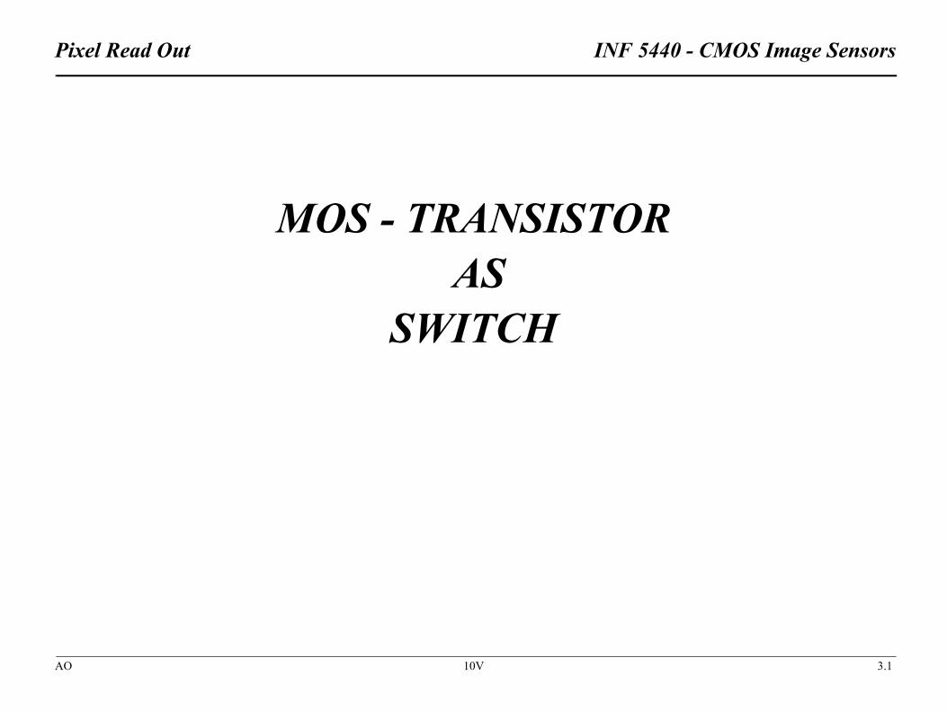
Ou
t -Id
INF 544
10V
endix: MOS Transistor
tput characteristics for PMOSt
-Vds,sa
-Vds
r0=∆Vds/∆Id
∆Id∆Vds
-Vg1
-Vg2
-Vg3
-Vg4
-Vg5
-Vds
Id
-Vg
Vs=0

0 - CMOS Image Sensors
AO 3.34
App
Mo
Ref.: Grove
INF 544
10V
endix: MOS Transistor
bility as a function of doping concentration

0 - CMOS Image Sensors
AO 3.35
App
SmTran
(3.A5)
Bulk T given by (3.A1))
(3.A6)
Outp
(3.A7)
(3.A8)
2µCoxWL-----ID=
gmVsb+
------------------
INF 544
10V
endix: MOS Transistor
all signal parameters:sconductans at constant VSB, VDS > VGS - VT. (Differentiate (3.A3))
transconductans at constant VGS, VDS > VGS - VT (Differentiate (3.A3) with V
ut conductance (differentiate (3.A2) and (3.A4)
gmdId
dVgs------------ 2
µCox2
-------------WL----- Vgs VT–[ ] 2µCox
WL-----
µCox2
-------------WL-----
Vgs VT–[ ]2== =
gmbdId
dVsb------------ dI
dVT-----------
dVTdVsb------------ 2
µCox2
-------------WL----- Vgs VT–[ ] γ
2ΦF Vsb+---------------------------------- γ
2ΦF----------------=== =
gddId
dVds------------ µCox
WL----- Vgs VT Vds––[ ]= = Vds Vgs VT–<
gddId
dVds------------
λIDS1 λVDS+( )
----------------------------- λIDS≈= = Vds Vgs VT–≥

0 - CMOS Image Sensors
AO 3.36
App
The
Ref.: Grove
INF 544
10V
endix: MOS Transistor
ratio gmb to gm

0 - CMOS Image Sensors
AO 3.37
App
CapFor
(3.A9)
(3.A10)
For
(3.A11)
(3.A12)
Sou
(3.A13)
A= a
INF 544
10V
endix: MOS Transistor
acitanceVds< Vgs-VT:
Vds> Vgs-VT:
(empiric)
rce - Drain junction capacitance (used in SPICE level=3):
rea, P=perimeter
Cgc CoxWL 2CovlW+=
Ccbεsixd------WL=
Cgs23---CoxWL CovlW+=
Cgd CovlW=
Cj A CJ⋅= 1VjPB-------–
MJ–P CJSW 1
VjPB-------–
MJSW–⋅+

0 - CMOS Image Sensors
AO 3.38
App
Sm
W
CdbgdsVsbgmb
quivalent
dIddVgs------------ 2µCox
WL-----Id= =
dIddVsb------------ 2µCchbulk
WL-----Id≈=
gdsdId
dVds------------ λId≈=
D
BS
ed, Vsbgmb= 0
INF 544
10V
endix: MOS Transistor
all signal equivalent
DrainSourceGate
L
Cgs Vgs
Vgsgm
Common Source erg
gm
gmb
Bulk
G
S
If S and B are connect

0 - CMOS Image Sensors
AO 3.39
App
Sm
V
gs gmb(-Vsb)
D
B
gd
Cdb
Cgs23---CoxWL Cgsovl+=
Cgd Cgdovl=
Cdb Junction=
INF 544
10V
endix: MOS Transistor
all signal equivalent (cont.)
ZL
Vsbg
Cgs
Cgd
Csb
Cdb
rg
gmV
G
Vgs
Vgs=Vg-Vsb
S
Cdb
CcbCsb
Cgs=Cgc+Cgs_ovl DrainSource
Cgd=Cgd_ovlGate
Vds-Vds,sat
Cgd
Cgs
Csb

0 - CMOS Image Sensors
AO 3.40
App
Tra
Drain
Source
Bulk
Drain
Source
N-typeP-typeP-type
nel MOS-transistor
V
VBulk athighvoltage
INF 544
10V
endix: MOS Transistor
nsistor symbols
Drain
Source
Gate Bulk
Drain
Source
Gate
Bulk: P-typeDrain: N-typeSource: N-type
N-channel MOS-transistor
Gate
Gate
Bulk: Drain: Source:
P-chan
V
VBulk grounded

0 - CMOS Image Sensors
AO 3.41
App
Dio
Give
it wi
beca
Inpu
Vds
Id
VdsVT
INF 544
10V
endix: MOS Transistor
de connected transistor
n that the transistor is in strong inversion,
,
ll always be saturated when VGS=VDS (connected)
use the condition: must be met
t conductance:
(3.A14)
Id
VGS VT≥
VDS VGS VT–≥
ginndId
dVds------------≡
dIddVgs------------ gm
1rinn---------= = =

0 - CMOS Image Sensors
AO 3.42
App
Cu
App
give
Idea
Theoutp
Iref Iut
M1 M2
INF 544
10V
endix: MOS Transistor
rrent mirrors • M1 is always saturated because Vds = Vgs > Vgs - VT
• Assuming M2 saturated as well
lying the expression for the drain current:
s the output current:
(3.A15)
lly for long channels (λ=0), and when L1=L2:
simple expression above is inaccurate for short channels due to the final ut resistance for M2. Therefore:
(3.A16)
Idµ0Cox
2----------------W
L----- Vgs VT–( )2 1 λVds+( )=
Iut
µ0Cox2
----------------W2L2-------- Vgs VT–( )2 1 λVds2+( )
µ0Cox2
----------------W1L1-------- Vgs VT–( )2 1 λVds1+( )
---------------------------------------------------------------------------------------IrefW2L1 1 λVds2+( )
L2W1 1 λVds1+( )---------------------------------------------Iref= =
IutW2W1--------Iref=
rut1
gM2----------= 1
dId2dVds2------------------------------ 1
µ0Cox2
----------------WL----- Vgs VT–( )2λ
---------------------------------------------------------1 λVds+( )
λId--------------------------- 1
λId--------≈= = =
0 - CMOS Image Sensors
AO 3.43
App
CasHav
Iref
gds
gsgm
Vsbgmb
gds
gsgm
Vsbgmb
D2
D4
2
Iutvut
gds2v3gmb2
gds4
vut
INF 544
10V
endix: MOS Transistor
coded current mirrorse high output resistance
M1 M2
M3 M4
Iut
R
v1
v2 v3
vut
Vgds
Vgsgm
Vsbgmb
gds
Vgsgm
Vsbgmb
V
G1 G2
G3 G4
D1
D3
S1 S
S3 S4
R
Irefv1
v3
(v1-v3)gm2
1/(gm1-gmb1+gds3)
v2gm4
Iref
S3
1/(gm3+gds3)
v1
v3v2

0 - CMOS Image Sensors
AO 3.44
App
Outp
The
Solv
(3.A17)
a( )b( )
s-
ds2
ds4
ut
INF 544
10V
endix: MOS Transistor
ut resistance rut = dvut / diut
DC voltages v1=v2=0 is zero in a small signal equivalent circuit:
ing (b) for v3 and replacing v3 in (a). Reorganizing gives:
iut gm2 v1 v3–( )– gmb2v3 gds2 vout v3–( )–+ 0=
gds4v3 gm4v2 gm2– v1 v3–( ) gds2 v3 vut–( ) gmb2v3+ + + 0=
rutvutiut-------
gm2 gmb2 gds2 gds4+ + +gds2gds4
----------------------------------------------------------------gm2
gds2gds4----------------------≈
gm2gds2---------- 1
λId---------= = =
g(v1-v3)gm2 v3gmb21/(gm1-gmb1+gds3)
gv2gm4
Iref
1/(gm3+gds3)
v1
v3
v
v2
0 - CMOS Image Sensors
AO 3.45
Ref
ras,
INF 544
10V
erences
TsividisOperation and Modelling of the MOS Transistor Yannis P. TsividisMcGraw-Hill Series in Electrical Engineering
GrovePhysics and Technology of Semiconductor DevicesA.S. GroveJohn Wiley & son
NakamuraImage Sensors and Signal Processing for Digital Still Cameedited by Junich NakamuraTaylor & Francis