![The Future of DMOs[1]](https://static.fdocuments.us/doc/165x107/577d29791a28ab4e1ea6e1ee/the-future-of-dmos1.jpg)
MOS Model 20 - nxp.com · Since a DMOS transistor is an asymmetric device, no source-drain...
61
Unclassified Technical Note PR-TN-2005/00406 Date of issue: May 2009 MOS Model 20 Level 2002.2 A.C.T. Aarts, A. Tajic, and S.J. Sque Unclassified Technical Note c NXP Semiconductors 2009
Transcript of MOS Model 20 - nxp.com · Since a DMOS transistor is an asymmetric device, no source-drain...

Unclassified Technical Note PR-TN-2005/00406
Date of issue: May 2009
MOS Model 20Level 2002.2
A.C.T. Aarts, A. Tajic, and S.J. Sque
Unclassified Technical Notec©NXP Semiconductors 2009

May 2009 MOS Model 20, Level 2002.2 Unclassified Technical Note PR-TN-2005/00406
Corresponding author: S.J. Sque, [email protected]
c©NXP Semiconductors 2009All rights are reserved. Reproduction in whole or in part is
prohibited without the written consent of the copyright owner.
ii c©NXP Semiconductors 2009

Unclassified Technical Note PR-TN-2005/00406 MOS Model 20, Level 2002.2 May 2009
Unclassified Technical Note: PR-TN-2005/00406
Title: MOS Model 20Level 2002.2
Author(s): A.C.T. Aarts, A. Tajic, and S.J. Sque
Part of project: Compact Modelling
Customer: NXP Semiconductors
Keywords: circuit simulation, compact modelling, DMOS, LDMOS, high voltageMOS, extended drain MOS, MOS Model 20, power integrated circuits
Abstract: The model description for the compact high-voltage MOS transistormodel called MOS Model 20 (MM20) is presented. MM20 has beendeveloped for circuit simulation of power integrated circuits. MM20describes the electrical behaviour of a high-voltage MOS device, likea Lateral Double-diffused MOS (LDMOS) device or an extended-drainMOSFET. The model combines the MOSFET operation of the channelregion with that of the drift region of such high-voltage devices.
Since MM20 is a surface-potential–based model, it gives an accurate de-scription in all operation regimes, ranging from sub-threshold to abovethreshold, in both the linear and saturation regime. MM20 includesstrong inversion, depletion, and accumulation, in both thechannel re-gion and the drift region of the device. In addition to the previousMM20 model (level = 2001), in this MM20 model (level = 2002), quasi-saturation is included, an effect which is typical for high-voltage LD-MOS devices.
The objective of this report is to present the full definitionof MM20,level = 2002, including the model parameter set, the temperature andgeometrical scaling rules, and all the implemented model equations forthe currents, charges, and noise sources. The parameter extraction strat-egy is briefly explained.
c©NXP Semiconductors 2009 iii

May 2009 MOS Model 20, Level 2002.2 Unclassified Technical Note PR-TN-2005/00406
Preface and History of Model and Documentation
Preface
The first version of the compact LDMOS model, MOS Model 20, became available in October2003. Future changes and additions to the model have been documented by extending or changingthe documentation in this report.
History of Model
October 2003 : Release of MOS Model 20, level 2001, test version.January 2004 : Update of MOS Model 20, level 2001, test version.
This update, for instance, omits the source-drain interchange for theDC current description.
October 2004 : Introduction of MOS Model 20, level 2001.This update includes some practical changes, like the pinch-offvoltageVoxp0, the clip-low values ofm and ofλD, and theimplementation of the noise transfer function.
May 2005 : Introduction of MOS Model 20, level 2002.This update includes velocity saturation in the drift region.
August 2006 : Update of MOS Model 20, level 2002.This update includes some practical changes, like the clip-lowvalues ofW andWD, and improved avalanche-current modelling.
February 2007 : Update of MOS Model 20, level 2002.Release of version 2002.2, which includes self-heating.
March 2008 : Update of MOS Model 20, level 2002.Several minor bugs fixed in version 2002.2 of the model.
History of Documentation
August 2003 : First documentation of MOS Model 20, level 2001, test version.January 2004 : Update of documentation of MOS Model 20, level 2001, test version,
according to the model formulation of January 2004.October 2004 : Introduction of MOS Model 20, level 2001.
This update includes some practical changes, like the pinch-offvoltageVoxp0, and the clip-low values ofm and ofλD.
May 2005 : Introduction of MOS Model 20, level 2002.This update includes velocity saturation in the drift region.
August 2006 : Update of documentation of MOS Model 20, level 2002.This update takes into account the contribution of both the channel anddrift regions to the weak-avalanche current.
March 2007 : Update of documentation of MOS Model 20, level 2002.This update includes a section on the parameter extraction strategy.
March 2008 : Update of documentation of MOS Model 20, level 2002.This update details aspects new to version 2002.2 and corrects minor errors.
May 2009 : Update of documentation of MOS Model 20, level 2002.This update corrects minor errors related to self-heating and temperature scaling.
iv c©NXP Semiconductors 2009

Unclassified Technical Note PR-TN-2005/00406 MOS Model 20, Level 2002.2 May 2009
Contents
1 Introduction 1
1.1 Structural Elements of MOS Model 20 . . . . . . . . . . . . . . . . . .. . . . . 3
1.2 Structure of this Report . . . . . . . . . . . . . . . . . . . . . . . . . . .. . . . 4
2 Embedding 5
2.1 External Electrical Quantities and Variables . . . . . . . .. . . . . . . . . . . . 5
2.2 Internal Electrical Quantities and Variables . . . . . . . .. . . . . . . . . . . . 6
2.3 Embedding Procedure of MOS Model 20 in a Circuit Simulator . . . . . . . . . 7
3 Nomenclature 11
3.1 Input Variables and Quantities . . . . . . . . . . . . . . . . . . . . .. . . . . . 11
3.1.1 List of Numerical Constants . . . . . . . . . . . . . . . . . . . . . .. . 11
3.1.2 List of Physical Constants . . . . . . . . . . . . . . . . . . . . . . .. . 11
3.1.3 List of Circuit Simulator Variables . . . . . . . . . . . . . . .. . . . . . 11
3.2 Geometrical Model . . . . . . . . . . . . . . . . . . . . . . . . . . . . . . . .. 12
3.2.1 List of Geometrical Model Parameters . . . . . . . . . . . . . .. . . . . 12
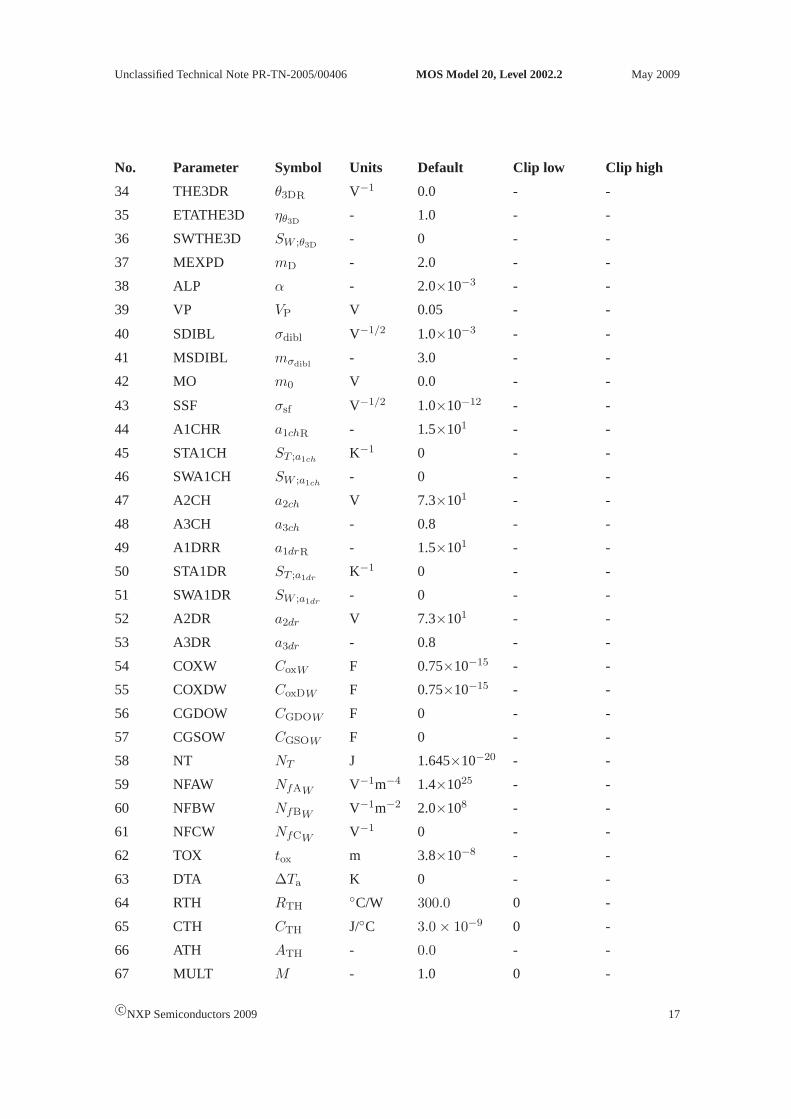
3.2.2 Default and Clipping Values of Geometrical Model Parameters . . . . . . 16
3.2.3 Geometry and Temperature Scaling . . . . . . . . . . . . . . . . .. . . 19
3.3 Electrical Model . . . . . . . . . . . . . . . . . . . . . . . . . . . . . . . . .. . 21
3.3.1 List of Electrical Model Parameters . . . . . . . . . . . . . . .. . . . . 21
3.3.2 Default and Clipping Values of Electrical Model Parameters . . . . . . . 24
3.3.3 Temperature Scaling . . . . . . . . . . . . . . . . . . . . . . . . . . . .26
3.4 Postprocessing . . . . . . . . . . . . . . . . . . . . . . . . . . . . . . . . . .. 27
3.4.1 MULT Scaling . . . . . . . . . . . . . . . . . . . . . . . . . . . . . . . 27
3.4.2 Clipping of Actual Parameters . . . . . . . . . . . . . . . . . . . .. . . 27
4 Implemented Equations 28
4.1 Internal Parameters . . . . . . . . . . . . . . . . . . . . . . . . . . . . . .. . . 28
4.2 Current Equations . . . . . . . . . . . . . . . . . . . . . . . . . . . . . . . .. . 29
4.3 Charge Equations . . . . . . . . . . . . . . . . . . . . . . . . . . . . . . . . .. 35
4.4 Noise Equations . . . . . . . . . . . . . . . . . . . . . . . . . . . . . . . . . .. 40
4.5 Self-Heating . . . . . . . . . . . . . . . . . . . . . . . . . . . . . . . . . . . .. 41
4.5.1 Equivalent Circuit . . . . . . . . . . . . . . . . . . . . . . . . . . . . .41
4.5.2 Model Equations . . . . . . . . . . . . . . . . . . . . . . . . . . . . . . 41
4.5.3 Usage . . . . . . . . . . . . . . . . . . . . . . . . . . . . . . . . . . . . 42
c©NXP Semiconductors 2009 v

May 2009 MOS Model 20, Level 2002.2 Unclassified Technical Note PR-TN-2005/00406
5 Parameter Extraction Strategy 44
5.1 Measurements . . . . . . . . . . . . . . . . . . . . . . . . . . . . . . . . . . . .44
5.2 Extraction of Miniset Parameters (including Temperature Scaling) . . . . . . . . 46
5.3 Extraction of Maxiset Parameters . . . . . . . . . . . . . . . . . . .. . . . . . . 49
6 Pstar-Specific Items 50
6.1 Syntax . . . . . . . . . . . . . . . . . . . . . . . . . . . . . . . . . . . . . . . . 50
6.2 DC Operating Point Output . . . . . . . . . . . . . . . . . . . . . . . . . .. . . 51
References 53
A Auxiliary Functions 55
vi c©NXP Semiconductors 2009

Unclassified Technical Note PR-TN-2005/00406 MOS Model 20, Level 2002.2 May 2009
1 Introduction
MOS Model 20 (MM20) is a compact MOSFET model intended for analogue circuit simulation inhigh-voltage MOS technologies. MOS Model 20 describes the electrical behaviour of the regionunder the thin gate oxide of a high-voltage MOS device, like aLateral Double-diffused MOS(LDMOS) device or an extended-drain MOSFET; see Figure 1. Itthus combines the MOSFEToperation of the channel region with that of the drift regionunder the thin gate oxide in a high-voltage MOS device. As such, MOS Model 20 is aimed as a successor of the combination of MOSModel 9 (MM9) [1] for the channel region in series with MOS Model 31 (MM31) [1] for the driftregion under the thin gate oxide, in macro models of various high-voltage MOS devices.
Di
pp−well
nn+ ++
DSB
G
n−
channel region drift region
Figure 1:The region under the thin gate oxide of ann-channel LDMOS device, described by MOSModel 20.
The model is based on the Silicon-on-Insulator (SOI)-LDMOSmodel developed by the Universityof Southampton [2]. MOS Model 20 has especially been developed to improve the convergencebehaviour during circuit simulation, by having the voltageat the transition (node Di) from thechannel region to the drift region calculated inside the model itself.
MOS Model 20 gives a complete description of all transistor-action–related quantities: nodal cur-rents, nodal charges, and noise-power spectral densities.The equations describing these quantitiesare based on surface-potential formulations, resulting inequations valid over all operation regimes(i.e. accumulation, depletion, and inversion in both the channel region and the drift region). Thesurface potential as a function of the terminal voltages is obtained by the explicit expression asderived in Ref. [3] and used in MOS Model 11 (MM11), level 1101[4]. Additionally, several im-portant physical effects have been included in the model: mobility reduction, velocity saturation,drain-induced barrier lowering, static feedback, channellength modulation, and weak avalanche(or impact ionization).
MOS Model 20 only provides a model for the intrinsic MOSFET behaviour of the region underthe thin gate oxide of a high-voltage MOS device, as well as the gate/source- and gate/drain over-lap regions. Junction charges, junction leakage currents,interconnect capacitances, and parasiticbipolar transistors are not included; they should be covered by separate models. For instance, todescribe the electrical behaviour due to the pn-junction between the backgate (B) and drain (D),an additional diode model for this pn-junction has to be added; see Figure 2. Furthermore, for veryhigh-voltage MOS transistors with an additional thick fieldoxide, like in Figure 3, MOS Model
c©NXP Semiconductors 2009 1

May 2009 MOS Model 20, Level 2002.2 Unclassified Technical Note PR-TN-2005/00406
20 can be used in series with a separate model for the drift region under the thick field oxide. Inthe case of the SOI-LDMOS transistor in Figure 3, MOS Model 40(MM40) [1] has been used tomodel the part of the drift region underneath the thick oxide. Finally, self-heating of the device,which may significantly affect the electrical behaviour, isnow included via a thermal network asof version 2002.2 of the model.
G
DSB 00
Figure 2:Macro model for an LDMOS transistor.
00 00%6
*
'
+:
Figure 3:Macro model for an SOI-LDMOS transistor with a thick field oxide.
2 c©NXP Semiconductors 2009

Unclassified Technical Note PR-TN-2005/00406 MOS Model 20, Level 2002.2 May 2009
1.1 Structural Elements of MOS Model 20
The structure of MOS Model 20 is the same as the structure of MOS Model 9 and MOS Model11. This structure can be divided into:
• Model embedding: It is convenient to use one single model for bothn- and p-channeldevices. For this reason, anyp-channel device and its bias conditions are mapped onto thoseof an equivalentn-channel transistor. This mapping comprises a number of sign changes.
Since a DMOS transistor is an asymmetric device, no source-drain interchange is appliedin case the external voltage mapped onto ann-channel transistor is negative. Thus, in MOSModel 20, the DC currents and charges are calculated by use ofthe externally applied volt-ages mapped onto an equivalentn-channel transistor.
• Preprocessing:The complete set of all the parameters, as they occur in the equations forthe various electrical quantities, is denoted as the set ofactual parameters. Since most ofthese actual parameters scale with temperature, and since self-heating is significant for high-voltage devices, each of them can be determined by electrical measurements over a range oftemperatures. The set of electrical parameters at a reference temperature including the tem-perature scaling parameters and reference temperature itself, is denoted as theminiset. Thisminiset forms the input for the so-calledelectrical model, from which the actual parametersfor an arbitrary temperature are obtained by applying the temperature scaling rules. Thesetemperature scaling rules thus describe the dependencies of the actual parameters on thetemperature of the device.
Since most of the electrical parameters also scale with geometry, the process as a wholeis characterized by an enlarged set of parameters, usually called themaxiset. This maxisetconsists of the transistor dimensions, the electrical parameters for certain device dimen-sions at a reference temperature, the reference temperature itself, and all temperature- andgeometry scaling parameters. Together, they form the inputfor the so-calledgeometricalmodel. From the maxiset parameters, the actual parameters for an arbitrary transistor areobtained by applying the temperature and geometry scaling rules. These scaling rules thusdescribe the dependencies of the actual parameters on the drift-region length, device width,and temperature of the device.
Since the application of the scaling rules is done only once,i.e. prior to the actual electricalsimulation, this procedure is calledpreprocessing.
• Clipping: To prevent the scaling rules from generating actual parameters that are outsidea physically realistic range or that create numerical difficulties (such as division by zero),the actual parameters may be clipped to a pre-specified range. This clipping of actual pa-rameters is doneafter the preprocessing. The pre-specified clipping ranges for the actualparameters are taken as those in the electrical model parameter list in Section 3.3.1.
Furthermore, in order to prevent numerical difficulties in the preprocessing procedure, themodel parameters of both the electrical and geometrical model may also be clipped to apre-specified range. This clipping of model parameters is done before the preprocessing.The pre-specified clipping ranges for both the electrical and geometrical model parametersare taken as those in the geometrical model parameter list inSection 3.2.1.
• Current equations: These are all expressions needed to obtain the DC nodal currents as afunction of the bias conditions. They can be separated into equations for the channel currentand the avalanche current.
c©NXP Semiconductors 2009 3

May 2009 MOS Model 20, Level 2002.2 Unclassified Technical Note PR-TN-2005/00406
• Charge equations:These are all the equations that are used to calculate both the intrinsicand extrinsic charge quantities, which are assigned to the nodes. They can be separated intoequations for the channel-region charges and the drift-region charges.
• Noise equations:The total noise output of a transistor consists of a thermal noise and aflicker noise part, which create fluctuations in the channel current. Owing to the capacitivecoupling between the gate and channel region, current fluctuations in the gate current areinduced as well, which are referred to as induced gate noise.
1.2 Structure of this Report
After this introductory section, the procedure of embedding MOS Model 20 in a circuit simulatoris outlined. Next, the nomenclature is explained, while in Section 4 the implemented equationsare listed. Finally the operating point output parameters are described.
4 c©NXP Semiconductors 2009

Unclassified Technical Note PR-TN-2005/00406 MOS Model 20, Level 2002.2 May 2009
2 Embedding
In high-voltage technologies, bothn- andp-channel LDMOS transistors are supported. It is con-venient to use one single model for both types of transistor instead of two separate models. Thisis accomplished by mapping ap-channel device with its bias conditions and parameter set onto anequivalentn-channel device with appropriately changed bias conditions (i.e. currents, voltages,and charges) and parameters. In this way, both types of transistor can be treated as ann-channeltransistor. In MOS Model 20, we let the electrons and holes have the same electrical behaviour.As a result, the same equations are used for bothn- andp-type transistors.
Since a DMOS transistor is an asymmetric device, no source-drain interchange is applied in casethe external voltage mapped onto ann-channel transistor is negative. Thus, in MOS Model 20, theDC currents and charges are calculated by use of the externally applied voltages mapped onto anequivalentn-channel transistor.
The total transformation procedure is explained in detail in Section 2.3.
2.1 External Electrical Quantities and Variables
No. Variable Program Units Description
Name
1 VeD VDE V Potential applied to the drain node
2 VeG VGE V Potential applied to the gate node
3 VeS VSE V Potential applied to the source node
4 VeB VBE V Potential applied to the bulk node
5 IeD IDE A DC current into the drain
6 IeG IGE A DC current into the gate
7 IeS ISE A DC current into the source
8 IeB IBE A DC current into the bulk
9 QeD QDE C Charge in the device attributed to the drain node
10 QeG QGE C Charge in the device attributed to the gate node
11 QeS QSE C Charge in the device attributed to the source node
12 QeB QBE C Charge in the device attributed to the bulk node
13 SeD SDE A2s Spectral density of the noise current into the drain
14 SeG SGE A2s Spectral density of the noise current into the gate
15 SeS SSE A2s Spectral density of the noise current into the source
16 SeDG SDGE A2s Cross spectral density between the drain and the gate
noise currents17 Se
GS SGSE A2s Cross spectral density between the gate and the sourcenoise currents
18 SeSD SSDE A2s Cross spectral density between the source and the
drain noise currents
c©NXP Semiconductors 2009 5

May 2009 MOS Model 20, Level 2002.2 Unclassified Technical Note PR-TN-2005/00406
The definitions of the external electrical variables are illustrated in Figure 4.
b
b
b
b
B
S
G
D
SeD
SeG
SeS
ieD
ieG
ieS
ieB
VeD
VeG
VeS
VeB
ieD = IeD +dQe
D
dt
ieG = IeG +dQe
G
dt
ieS = IeS +dQe
S
dt
ieB = IeB +dQe
B
dt
Figure 4: Definition of the external electrical quantities and variables.
2.2 Internal Electrical Quantities and Variables
No. Variable Program Units Description
Name
1 VDS VDS V Drain-to-source voltage applied to the equivalentn-MOST
2 VGS VGS V Gate-to-source voltage applied to the equivalentn-MOST
3 VSB VSB V Source-to-bulk voltage applied to the equivalentn-MOST
4 IDS IDS A DC current through the channel flowing from drain tosource
5 IAVL IAVL A DC current flowing from drain to bulk due to theweak-avalanche effect
6 QD QD C Intrinsic charge in the equivalentn-MOST attributedto the drain node
7 QG QG C Intrinsic charge in the equivalentn-MOST attributedto the gate node
8 QS QS C Intrinsic charge in the equivalentn-MOST attributedto the source node
9 QB QB C Intrinsic charge in the equivalentn-MOST attributedto the bulk node
6 c©NXP Semiconductors 2009

Unclassified Technical Note PR-TN-2005/00406 MOS Model 20, Level 2002.2 May 2009
10 SDthSDTH A2s Spectral density of the thermal-noise current of the
channel region
11 SDflSDFL A2s Spectral density of the flicker-noise current of the
channel region
12 SGthSGTH A2s Spectral density of the thermal-noise current induced
in the gate
13 SGDthSGDTH A2s Cross spectral density of the thermal-noise current in-
duced in the gate and the thermal-noise current of thechannel
2.3 Embedding Procedure of MOS Model 20 in a Circuit Simulator
In order to embed MOS Model 20 correctly into a circuit simulator, the following procedure(illustrated in detail in Figure 2.3) should be followed. Wehave assumed that indeed the simulatorprovides the nodal potentialsVe
D, VeG, Ve
S, andVeB based on ana priori assignment of drain, gate,
source, and bulk. As a DMOS is an asymmetric device, no source-drain interchange is applied asis done in a conventional (symmetric) MOSFET. The followingsteps are taken:
1. Calculate the voltagesV”DS, V”
GS, andV”SB, and the additional voltagesV”
DG andV”SG. The
latter are used for calculating the charges associated withoverlap capacitances.
2. Based onn- or p-channel devices, calculate the modified voltagesVDS, VGS, andVSB. Fromhere onwards, onlyn-channel behaviour needs to be considered.
3. Evaluate all the internal output quantities – channel current, weak-avalanche current, nodalcharges, and noise-power spectral densities – using the MOSModel 20 equations and thecorresponding voltages.
4. Correct for a possiblep-channel transformation.
5. Change from branch current to nodal currents, establishing the external current output quan-tities. Add the overlap charges to the nodal charges, thus forming the external charge outputquantities.
c©NXP Semiconductors 2009 7

May 2009 MOS Model 20, Level 2002.2 Unclassified Technical Note PR-TN-2005/00406
VeD, Ve
G, VeS, Ve
B
?V”
DS = VeD − Ve
S
V”GS = Ve
G − VeS
V”SB = Ve
S − VeB
V”DG = Ve
D − VeG
V”SG = Ve
S − VeG
n-channel Channel p-channeltype
@@@
@@@
?
VDS = V”DS
VGS = V”GS
VSB = V”SB
VDS = −V”DS
VGS = −V”GS
VSB = −V”SB
?
IDS = IDS (VDS ,VGS,VSB)
IAVL = IAVL (VDS ,VGS,VSB)
QD = QD (VDS ,VGS,VSB)
QS = QS (VDS ,VGS,VSB)
QG = QG (VDS ,VGS,VSB)
QB = − (QD + QS + QG)
SDfl= SDfl
(VDS ,VGS,VSB)
SDth= SDth
(VDS ,VGS,VSB)
SGth= SGth
(VDS ,VGS,VSB)
SGDth= SGDth
(VDS ,VGS,VSB)
8 c©NXP Semiconductors 2009

Unclassified Technical Note PR-TN-2005/00406 MOS Model 20, Level 2002.2 May 2009
?
A
yes VDS ≥ 0 no
@@@
@@@
I’DB = IAVL
I’SB = 0
S’D = SDfl
+ SDth
S’G = SGth
S’S = SDfl
+ SDth+ SGth
+ 2Re
SGDth
S’DG = S*
GDth
S’GS = −SGth
− SGDth
S’SD = −SGDth
− SDfl− SDth
I’DB = 0
I’SB = IAVL
S’D = SDth
+ SDfl+ SGth
+ 2Re
SGDth
S’G = SGth
S’S = SDfl
+ SDth
S’DG = −SGth
− S*GDth
S’GS = SGDth
S’SD = −S*
GDth− SDth
− SDfl
n-channel Channel p-channeltype
@@@
@@@
?
I”DS = IDS
I”DB = I’DB
I”SB = I’SB
Q”D = QD
Q”G = QG
Q”S = QS
Q”B = QB
S”D = S’
D
S”G = S’
G
S”S = S’
S
S”DG = S’
DG
S”GS = S’
GS
S”SD = S’
SD
I”DS = −IDS
I”DB = −I’DB
I”SB = −I’SB
Q”D = −QD
Q”G = −QG
Q”S = −QS
Q”B = −QB
S”D = S’
D
S”G = S’
G
S”S = S’
S
S”DG = S’
DG
S”GS = S’
GS
S”SD = S’
SD
?B
c©NXP Semiconductors 2009 9

May 2009 MOS Model 20, Level 2002.2 Unclassified Technical Note PR-TN-2005/00406
?
B
IeD = I”DS + I”DB
IeG = 0
IeS = −I”DS + I”SB
IeB = −I”DB − I”SB
QeD = Q”
D + CGDO · V”DG
QeG = Q”
G − CGDO · V”DG − CGSO · V”
SG
QeS = Q”
S + CGSO · V”SG
QeB = Q”
B
SeD = S”
D
SeG = S”
G
SeS = S”
S
SeDG = S”
DG
SeGS = S”
GS
SeSD = S”
SD
?IeD IeG IeS IeB Qe
D QeG Qe
S QeB Se
D SeG Se
S SeDG Se
GS SeSD
Figure 5: Transformation scheme.
It is customary to have separate user models in the circuit simulators forn- andp-channel transis-tors. In that manner, it is easy to use a different set of reference and scaling parameters for the twochannel types. As a consequence, the changes in the parameter values necessary for ap-channeltype transistor are normally already included in the parameter sets on file. The changes should notbe included in the simulator.
10 c©NXP Semiconductors 2009

Unclassified Technical Note PR-TN-2005/00406 MOS Model 20, Level 2002.2 May 2009
3 Nomenclature
3.1 Input Variables and Quantities
3.1.1 List of Numerical Constants
No. Constant Program name Value
1 A LN MINDOUBLE −800
3.1.2 List of Physical Constants
No. Constant Program name Value Units
1 T0 KELVIN CONVERSION 273.15 KOffset for conversion from Celsius to Kelvin temperature scale
2 kB K BOLTZMANN 1.3806226 · 10−23 JK−1
Boltzmann constant
3 q Q ELECTRON 1.6021918 · 10−19 CElementary unit charge
4 ǫox PHY EPSOX 3.4531438 · 10−11 Fm−1
Absolute permittivity of the oxide layer
3.1.3 List of Circuit Simulator Variables
No. Symbol Program name Units Description
1 Ta Ta C Ambient circuit temperature
2 f F Hz Operation frequency
c©NXP Semiconductors 2009 11

May 2009 MOS Model 20, Level 2002.2 Unclassified Technical Note PR-TN-2005/00406
3.2 Geometrical Model
To characterize a high-voltage MOS process as a whole, the geometrical model can be used. Thismodel uses as input the actual transistor dimensions, the electrical parameters for a referencedevice dimension and temperature, the reference temperature, and all temperature- and geometry-scaling parameters, together referred to as themaxiset. The model parameters of the geometricalmodel are listed in Section 3.2.1, while its scaling rules are listed in Section 3.2.3. For simplicity,in the geometrical MOS Model 20, bothn-channel andp-channel devices have been assigned thesame default parameter values.
3.2.1 List of Geometrical Model Parameters
No. Parameter Symbol Units Meaning
0 LEVEL level - Must be set to 2002
1 W W m Drawn width of the channel region
2 WVAR ∆W m Width offset of the channel region
3 WD WD m Drawn width of the drift region
4 WDVAR ∆WD m Width offset of the drift region
5 TREF TrefC Reference temperature
6 VFB VFB V Flat-band voltage of the channel region, at referencetemperature
7 STVFB ST ;VFBVK−1 Temperature scaling coefficient forVFB
8 VFBD VFBD V Flat-band voltage of the drift region, at reference tem-perature
9 STVFBD ST ;VFBDVK−1 Temperature scaling coefficient forVFBD
10 KOR k0R V1/2 Body factor of the channel region of an infinitely widetransistor
11 SWKO SW ;k0- Width scaling coefficient fork0
12 KODR k0DR V1/2 Body factor of the drift region of an infinitely widetransistor
13 SWKOD SW ;k0D- Width scaling coefficient fork0D
14 PHIB φB V Surface potential at the onset of strong inversion in thechannel region, at reference temperature
15 STPHIB ST ;φBVK−1 Temperature scaling coefficient forφB
16 PHIBD φBD V Surface potential at the onset of strong inversion in thedrift region, at reference temperature
17 STPHIBD ST ;φBDVK−1 Temperature scaling coefficient forφBD
18 BETW βW AV−2 Gain factor of a channel region of 1µm width, at ref-erence temperature
19 ETABET ηβ - Temperature scaling exponent forβ
12 c©NXP Semiconductors 2009

Unclassified Technical Note PR-TN-2005/00406 MOS Model 20, Level 2002.2 May 2009
No. Parameter Symbol Units Meaning
20 BETACCW βaccW AV−2 Gain factor of a drift region of 1µm width, at referencetemperature
21 ETABETACC ηβacc- Temperature scaling exponent forβacc
22 RDW RDW Ω On-resistance of a drift region of 1µm width, at refer-ence temperature
23 ETARD ηRD- Temperature scaling exponent forRD
24 LAMD λD - Quotient of the depletion layer thickness to the effec-tive thickness of the drift region atVSB = 0 V
25 THE1R θ1R V−1 Mobility reduction coefficient of an infinitely widetransistor, due to the vertical strong-inversion field inthe channel region
26 SWTHE1 SW ;θ1- Width scaling coefficient forθ1
27 THE1ACC θ1acc V−1 Mobility reduction coefficient in the drift region due tothe vertical electrical field caused by accumulation
28 THE2R θ2R V−1/2 Mobility reduction coefficient forVSB > 0 of an in-finitely wide transistor, due to the vertical depletionfield in the channel region
29 SWTHE2 SW ;θ2- Width scaling coefficient forθ2
30 THE3R θ3R V−1 Mobility reduction coefficient in the channel region ofan infinitely wide transistor, due to velocity saturation
31 ETATHE3 ηθ3- Temperature scaling exponent forθ3
32 SWTHE3 SW ;θ3- Width scaling coefficient forθ3
33 MEXP m - Smoothing factor for the transition from the linear tothe saturation regime
34 THE3DR θ3DR V−1 Mobility reduction coefficient in the drift region of aninfinitely wide transistor, due to velocity saturation
35 ETATHE3D ηθ3D- Temperature scaling exponent forθ3D
36 SWTHE3D SW ;θ3D- Width scaling coefficient forθ3D
37 MEXPD mD - Smoothing factor for the transition from the linear tothe quasi-saturation regime
38 ALP α - Factor for channel-length modulation
39 VP VP V Characteristic voltage of channel-length modulation
40 SDIBL σdibl V−1/2 Factor for drain-induced barrier lowering
41 MSDIBL mσdibl- Exponent for the drain-induced barrier lowering de-
pendence on the backgate bias
42 MO m0 V Parameter for the (short-channel) sub-threshold slope
43 SSF σsf V−1/2 Factor for static feedback
c©NXP Semiconductors 2009 13

May 2009 MOS Model 20, Level 2002.2 Unclassified Technical Note PR-TN-2005/00406
No. Parameter Symbol Units Meaning
44 A1CHR a1chR - Factor of weak-avalanche current of an infinitely widetransistor, at reference temperature, accounting for thecontribution of the channel region to the total avalanchecurrent
45 STA1CH ST ;a1chK−1 Temperature scaling coefficient fora1ch
46 SWA1CH SW ;a1ch- Width scaling coefficient fora1ch
47 A2CH a2ch V Exponent of channel-related weak-avalanche current
48 A3CH a3ch - Factor of the internal-drain–source voltage abovewhich weak avalanche occurs
49 A1DRR a1drR - Factor of weak-avalanche current of an infinitely widetransistor, at reference temperature, accounting for thecontribution of the drift region to the total avalanchecurrent
50 STA1DR ST ;a1drK−1 Temperature scaling coefficient fora1dr
51 SWA1DR SW ;a1dr- Width scaling coefficient fora1dr
52 A2DR a2dr V Exponent of drift-region weak-avalanche current
53 A3DR a3dr - Factor of the drain-source voltage above which weakavalanche occurs
54 COXW CoxW F Oxide capacitance for an intrinsic channel region of1 µm width
55 COXDW CoxDW F Oxide capacitance for an intrinsic drift region of 1µmwidth
56 CGDOW CGDOW F Gate-to-drain overlap capacitance for a drift region of1 µm width
57 CGSOW CGSOW F Gate-to-source overlap capacitance for a channel re-gion of 1µm width
58 NT NT J Coefficient of thermal noise, at reference temperature
59 NFAW NfAW V−1m−4 First coefficient of flicker noise for a channel region of1 µm width
60 NFBW NfBW V−1m−2 Second coefficient of flicker noise for a channel regionof 1 µm width
61 NFCW NfCW V−1 Third coefficient of flicker noise for a channel regionof 1 µm width
62 TOX tox m Thickness of the oxide above the channel region
63 DTA ∆Ta K Temperature offset to the ambient temperature
64 MULT M - Number of devices in parallel
14 c©NXP Semiconductors 2009

Unclassified Technical Note PR-TN-2005/00406 MOS Model 20, Level 2002.2 May 2009
The additional parameters for the model including self-heating are listed below.
No. Parameter Symbol Units Meaning
64 RTH RTHC/W Thermal resistance
65 CTH CTH J/C Thermal capacitance
66 ATH ATH - Thermal coefficient of the thermal resistance
The parameter MULT for all level-2002 models is detailed here:
No. Parameter Symbol Units Meaning
67 MULT M - Number of devices in parallel
c©NXP Semiconductors 2009 15

May 2009 MOS Model 20, Level 2002.2 Unclassified Technical Note PR-TN-2005/00406
3.2.2 Default and Clipping Values of Geometrical Model Parameters
No. Parameter Symbol Units Default Clip low Clip high
0 LEVEL level - 2002 - -
1 W W m 20×10−6 1.0×10⁻⁹ -
2 WVAR ∆W m 0 - -
3 WD WD m 20×10−6 1.0×10⁻⁹ -
4 WDVAR ∆WD m 0 -
5 TREF TrefC 25 −273 -
6 VFB VFB V −1.0 - -
7 STVFB ST ;VFBVK−1 0 - -
8 VFBD VFBD V −0.1 - -
9 STVFBD ST ;VFBDVK−1 0 - -
10 KOR k0R V1/2 1.6 - -
11 SWKO SW ;k0- 0 - -
12 KODR k0DR V1/2 1.0 - -
13 SWKOD SW ;k0D- 0 - -
14 PHIB φB V 0.86 - -
15 STPHIB ST ;φBVK−1 −1.2×10⁻³ - -
16 PHIBD φBD V 0.78 - -
17 STPHIBD ST ;φBDVK−1 −1.2×10⁻³ - -
18 BETW βW AV−2 7.0×10⁻⁵ - -
19 ETABET ηβ - 1.6 - -
20 BETACCW βaccW AV−2 7.0×10⁻⁵ - -
21 ETABETACC ηβacc- 1.5 - -
22 RDW RDW Ω 4.0×10³ - -
23 ETARD ηRD- 1.5 - -
24 LAMD λD - 0.2 - -
25 THE1R θ1R V−1 0.09 - -
26 SWTHE1 SW ;θ1- 0 - -
27 THE1ACC θ1acc V−1 0.02 - -
28 THE2R θ2R V−1/2 0.03 - -
29 SWTHE2 SW ;θ2- 0 - -
30 THE3R θ3R V−1 0.4 - -
31 ETATHE3 ηθ3- 1.0 - -
32 SWTHE3 SW ;θ3- 0 - -
33 MEXP m - 2.0 - -
16 c©NXP Semiconductors 2009
Unclassified Technical Note PR-TN-2005/00406 MOS Model 20, Level 2002.2 May 2009
No. Parameter Symbol Units Default Clip low Clip high
34 THE3DR θ3DR V−1 0.0 - -
35 ETATHE3D ηθ3D- 1.0 - -
36 SWTHE3D SW ;θ3D- 0 - -
37 MEXPD mD - 2.0 - -
38 ALP α - 2.0×10⁻³ - -
39 VP VP V 0.05 - -
40 SDIBL σdibl V−1/2 1.0×10⁻³ - -
41 MSDIBL mσdibl- 3.0 - -
42 MO m0 V 0.0 - -
43 SSF σsf V−1/2 1.0×10⁻¹² - -
44 A1CHR a1chR - 1.5×101 - -
45 STA1CH ST ;a1chK−1 0 - -
46 SWA1CH SW ;a1ch- 0 - -
47 A2CH a2ch V 7.3×101 - -
48 A3CH a3ch - 0.8 - -
49 A1DRR a1drR - 1.5×101 - -
50 STA1DR ST ;a1drK−1 0 - -
51 SWA1DR SW ;a1dr- 0 - -
52 A2DR a2dr V 7.3×101 - -
53 A3DR a3dr - 0.8 - -
54 COXW CoxW F 0.75×10⁻¹⁵ - -
55 COXDW CoxDW F 0.75×10⁻¹⁵ - -
56 CGDOW CGDOW F 0 - -
57 CGSOW CGSOW F 0 - -
58 NT NT J 1.645×10⁻²⁰ - -
59 NFAW NfAW V−1m−4 1.4×1025 - -
60 NFBW NfBW V−1m−2 2.0×10⁸ - -
61 NFCW NfCW V−1 0 - -
62 TOX tox m 3.8×10⁻⁸ - -
63 DTA ∆Ta K 0 - -
64 RTH RTHC/W 300.0 0 -
65 CTH CTH J/C 3.0 × 10⁻⁹ 0 -
66 ATH ATH - 0.0 - -
67 MULT M - 1.0 0 -
c©NXP Semiconductors 2009 17

May 2009 MOS Model 20, Level 2002.2 Unclassified Technical Note PR-TN-2005/00406
18 c©NXP Semiconductors 2009

Unclassified Technical Note PR-TN-2005/00406 MOS Model 20, Level 2002.2 May 2009
3.2.3 Geometry and Temperature Scaling
Effective temperature and dimensions:
TKamb = T0 + Ta + ∆Ta (3.1)
TKdev = T0 + Ta + ∆Ta + VdT (3.2)
TKref = T0 + Tref (3.3)
∆T = TKdev − TKref (3.4)
WE = W + ∆W (3.5)
WED = WD + ∆WD (3.6)
WEN = 1.0 × 10⁻⁶ (m) (3.7)
Actual parameters:
φT =kB · TKdev
q(3.8)
VFBT = VFB + ∆T · ST ;VFB(3.9)
VFBDT = VFBD + ∆T · ST ;VFBD(3.10)
k0 = k0R ·(
1 +WEN
WE· SW ;k0
)
(3.11)
k0D = k0DR ·(
1 +WEN
WED· SW ;k0D
)
(3.12)
φBT = φB + ∆T · ST ;φB(3.13)
φBDT = φBD + ∆T · ST ;φBD(3.14)
βT = βW · WE
WEN·(
TKref
TKdev
)ηβ
(3.15)
βaccT = βaccW · WED
WEN·(
TKref
TKdev
)ηβacc
(3.16)
RDT = RDW · WEN
WED·(
TKdev
TKref
)ηRD
(3.17)
θ1 = θ1R ·(
1 +WEN
WE· SW ;θ1
)
(3.18)
θ2 = θ2R ·(
1 +WEN
WE· SW ;θ2
)
(3.19)
c©NXP Semiconductors 2009 19

May 2009 MOS Model 20, Level 2002.2 Unclassified Technical Note PR-TN-2005/00406
θ3T = θ3R ·(
TKref
TKdev
)ηθ3
·(
1 +WEN
WE· SW ;θ3
)
(3.20)
θ3DT = θ3DR ·(
TKref
TKdev
)ηθ3D
·(
1 +WEN
WED· SW ;θ3D
)
(3.21)
a1chT = a1chR · (1 + ∆T · ST ;a1ch) ·(
1 +WEN
WE· SW ;a1ch
)
(3.22)
a1drT = a1drR · (1 + ∆T · ST ;a1dr) ·(
1 +WEN
WED· SW ;a1dr
)
(3.23)
Cox = CoxW · WE
WEN(3.24)
CoxD = CoxDW · WED
WEN(3.25)
CGDO = CGDOW · WED
WEN(3.26)
CGSO = CGSOW · WE
WEN(3.27)
NTT= NT · TKdev
TKref(3.28)
NfA = NfAW · WEN
WE(3.29)
NfB = NfBW · WEN
WE(3.30)
NfC = NfCW · WEN
WE(3.31)
RTHT= RTH ·
(
TKamb
TKref
)ATH
(3.32)
20 c©NXP Semiconductors 2009

Unclassified Technical Note PR-TN-2005/00406 MOS Model 20, Level 2002.2 May 2009
3.3 Electrical Model
To characterize a single LDMOS device including self-heating effects, the electrical model can beused. This model uses as input the electrical parameters fora reference temperature, the referencetemperature, and all temperature-scaling parameters, together referred to as theminiset. The modelparameters of the electrical model are listed in Section 3.3.1, while its temperature scaling rulesare listed in Section 3.3.3. For simplicity, in the electrical MOS Model 20, bothn-channel andp-channel devices have been assigned the same default parameter values.
3.3.1 List of Electrical Model Parameters
No. Parameter Symbol Units Meaning
0 LEVEL level - Must be set to 2002
1 TREF TrefC Reference temperature
2 VFB VFB V Flat-band voltage of the channel region, at referencetemperature
3 STVFB ST ;VFBVK−1 Temperature scaling coefficient forVFB
4 VFBD VFBD V Flat-band voltage of the drift region, at reference tem-perature
5 STVFBD ST ;VFBDVK−1 Temperature scaling coefficient forVFBD
6 KO k0 V1/2 Body factor of the channel region
7 KOD k0D V1/2 Body factor of the drift region
8 PHIB φB V Surface potential at the onset of strong inversion in thechannel region, at reference temperature
9 STPHIB ST ;φBVK−1 Temperature scaling coefficient forφB
10 PHIBD φBD V Surface potential at the onset of strong inversion in thedrift region, at reference temperature
11 STPHIBD ST ;φBDVK−1 Temperature scaling coefficient forφBD
12 BET β AV−2 Gain factor of the channel region, at reference temper-ature
13 ETABET ηβ - Temperature scaling exponent forβ
14 BETACC βacc AV−2 Gain factor for accumulation in the drift region, at ref-erence temperature
15 ETABETACC ηβacc- Temperature scaling exponent forβacc
16 RD RD Ω On-resistance of the drift region, at reference tempera-ture
17 ETARD ηRD- Temperature scaling exponent forRD
18 LAMD λD - Quotient of the depletion layer thickness atVSB > 0 tothe effective thickness of the drift region atVSB = 0 V
19 THE1 θ1 V−1 Mobility reduction coefficient in the channel regiondue to the vertical electrical field caused by strong in-version
c©NXP Semiconductors 2009 21

May 2009 MOS Model 20, Level 2002.2 Unclassified Technical Note PR-TN-2005/00406
No. Parameter Symbol Units Meaning
20 THE1ACC θ1acc V−1 Mobility reduction coefficient in the drift region due tothe vertical electrical field caused by accumulation
21 THE2 θ2 V−1/2 Mobility reduction coefficient atVSB > 0 in the chan-nel region due to the vertical electrical field caused bydepletion
22 THE3 θ3 V−1 Mobility reduction coefficient in the channel regiondue to the horizontal electrical field caused by veloc-ity saturation
23 ETATHE3 ηθ3- Temperature scaling exponent forθ3
24 MEXP m - Smoothing factor for the transition from the linear tothe saturation regime
25 THE3D θ3D V−1 Mobility reduction coefficient in the drift region due tothe horizontal electrical field caused by velocity satu-ration
26 ETATHE3D ηθ3D- Temperature scaling exponent forθ3D
27 MEXPD mD - Smoothing factor for the transition from the linear tothe quasi-saturation regime
28 ALP α - Factor for channel-length modulation
29 VP VP V Characteristic voltage of channel-length modulation
30 SDIBL σdibl V−1/2 Factor for drain-induced barrier lowering
31 MSDIBL mσdibl- Exponent for the drain-induced barrier lowering de-
pendence on backgate bias
32 MO m0 V Parameter for the (short-channel) sub-threshold slope
33 SSF σsf V−1/2 Factor for static feedback
34 A1CH a1ch - Factor of weak-avalanche current, at reference temper-ature, accounting for the contribution of the channelregion to the total avalanche current
35 STA1CH ST ;a1chK−1 Temperature scaling coefficient fora1ch
36 A2CH a2ch V Exponent of channel-related weak-avalanche current
37 A3CH a3ch - Factor of internal drain-source voltage above whichweak avalanche occurs
38 A1DR a1dr - Factor of weak-avalanche current, at reference temper-ature, accounting for the contribution of the drift regionto the total avalanche current
39 STA1DR ST ;a1drK−1 Temperature scaling coefficient fora1dr
40 A2DR a2dr V Exponent of drift-region weak-avalanche current
41 A3DR a3dr - Factor of drain-source voltage above which weakavalanche occurs
42 COX Cox F Oxide capacitance for the intrinsic channel region
22 c©NXP Semiconductors 2009

Unclassified Technical Note PR-TN-2005/00406 MOS Model 20, Level 2002.2 May 2009
No. Parameter Symbol Units Meaning
43 COXD CoxD F Oxide capacitance for the intrinsic drift region
44 CGDO CGDO F Gate-to-drain overlap capacitance
45 CGSO CGSO F Gate-to-source overlap capacitance
46 NT NT J Coefficient of thermal noise, at reference temperature
47 NFA NfA V−1m−4 First coefficient of flicker noise
48 NFB NfB V−1m−2 Second coefficient of flicker noise
49 NFC NfC V−1 Third coefficient of flicker noise
50 TOX tox m Thickness of the oxide above the channel region
51 DTA ∆Ta K Temperature offset to the ambient temperature
52 RTH RTHC/W Thermal resistance
53 CTH CTH J/C Thermal capacitance
54 ATH ATH - Thermal coefficient of the thermal resistance
55 MULT M - Number of devices in parallel
c©NXP Semiconductors 2009 23

May 2009 MOS Model 20, Level 2002.2 Unclassified Technical Note PR-TN-2005/00406
3.3.2 Default and Clipping Values of Electrical Model Parameters
No. Parameter Symbol Units Default Clip low Clip high
0 LEVEL level - 2002 - -
1 TREF TrefC 25 −273 -
2 VFB VFB V −1.0 - -
3 STVFB ST ;VFBVK−1 0 - -
4 VFBD VFBD V −0.1 - -
5 STVFBD ST ;VFBDVK−1 0 - -
6 KO k0 V1/2 1.6 1.0×10⁻¹² -
7 KOD k0D V1/2 1.0 1.0×10⁻¹² -
8 PHIB φB V 0.86 1.0×10⁻¹² -
9 STPHIB ST ;φBVK−1 −1.2×10⁻³ - -
10 PHIBD φBD V 0.78 1.0×10⁻¹² -
11 STPHIBD ST ;φBDVK−1 −1.2×10⁻³ - -
12 BET β AV−2 1.4×10⁻³ 1.0×10⁻¹² -
13 ETABET ηβ - 1.6 - -
14 BETACC βacc AV−2 1.4×10⁻³ 1.0×10⁻¹² -
15 ETABETACC ηβacc- 1.5 - -
16 RD RD Ω 2.0×10² 1.0×10⁻¹² -
17 ETARD ηRD- 1.5 - -
18 LAMD λD - 0.2 1.0×10⁻¹² -
19 THE1 θ1 V−1 0.09 0 -
20 THE1ACC θ1acc V−1 0.02 0 -
21 THE2 θ2 V−1/2 0.03 0 -
22 THE3 θ3 V−1 0.4 0 -
23 ETATHE3 ηθ3- 1.0 - -
24 MEXP m - 2.0 0.05 -
25 THE3D θ3D V−1 0.0 0 -
26 ETATHE3D ηθ3D- 1.0 - -
27 MEXPD mD - 2.0 0.05 -
28 ALP α - 2.0×10⁻³ 0 -
29 VP VP V 0.05 1.0×10⁻¹² -
30 SDIBL σdibl V−1/2 1.0×10⁻³ 0 -
31 MSDIBL mσdibl- 3.0 0 -
32 MO m0 V 0.0 0 0.5
33 SSF σsf V−1/2 1.0×10⁻¹² 1.0×10⁻¹² -
24 c©NXP Semiconductors 2009

Unclassified Technical Note PR-TN-2005/00406 MOS Model 20, Level 2002.2 May 2009
No. Parameter Symbol Units Default Clip low Clip high
34 A1CH a1ch - 1.5×101 0 -
35 STA1CH ST ;a1chK−1 0 - -
36 A2CH a2ch V 7.3×101 1.0×10⁻¹² -
37 A3CH a3ch - 0.8 0 -
38 A1DR a1dr - 1.5×101 0 -
39 STA1DR ST ;a1drK−1 0 - -
40 A2DR a2dr V 7.3×101 1.0×10⁻¹² -
41 A3DR a3dr - 0.8 0 -
42 COX Cox F 15×10−15 0 -
43 COXD CoxD F 15×10−15 0 -
44 CGDO CGDO F 0 0 -
45 CGSO CGSO F 0 0 -
46 NT NT J 1.645×10⁻²⁰ 0 -
47 NFA NfA V−1m−4 7.0×10²³ 0 -
48 NFB NfB V−1m−2 1.0×10⁷ 0 -
49 NFC NfC V−1 0 0 -
50 TOX tox m 3.8×10⁻⁸ 1.0×10⁻¹² -
51 DTA ∆Ta K 0 - -
52 RTH RTHC/W 300.0 0 -
53 CTH CTH J/C 3.0 × 10⁻⁹ 0 -
54 ATH ATH - 0.0 - -
55 MULT M - 1.0 0 -
c©NXP Semiconductors 2009 25

May 2009 MOS Model 20, Level 2002.2 Unclassified Technical Note PR-TN-2005/00406
3.3.3 Temperature Scaling
Effective temperature:
TKamb = T0 + Ta + ∆Ta (3.33)
TKdev = T0 + Ta + ∆Ta + VdT (3.34)
TKref = T0 + Tref (3.35)
∆T = TKdev − TKref (3.36)
Actual parameters:
φT =kB · TKdev
q(3.37)
VFBT = VFB + ∆T · ST ;VFB(3.38)
VFBDT = VFBD + ∆T · ST ;VFBD(3.39)
φBT = φB + ∆T · ST ;φB(3.40)
φBDT = φBD + ∆T · ST ;φBD(3.41)
βT = β ·(
TKref
TKdev
)ηβ
(3.42)
βaccT = βacc ·(
TKref
TKdev
)ηβacc
(3.43)
RDT = RD ·(
TKdev
TKref
)ηRD
(3.44)
θ3T = θ3 ·(
TKref
TKdev
)ηθ3
(3.45)
θ3DT = θ3D ·(
TKref
TKdev
)ηθ3D
(3.46)
a1chT = a1ch · (1 + ∆T · ST ;a1ch) (3.47)
a1drT = a1dr · (1 + ∆T · ST ;a1dr) (3.48)
NTT= NT · TKdev
TKref(3.49)
RTHT= RTH ·
(
TKamb
TKref
)ATH
(3.50)
26 c©NXP Semiconductors 2009

Unclassified Technical Note PR-TN-2005/00406 MOS Model 20, Level 2002.2 May 2009
3.4 Postprocessing
3.4.1 MULT Scaling
Since equal, parallel-circuited transistors are frequently employed in circuit design, the specifica-tion of one transistor together with a multiplication factor MULT (M ) in the circuit description isconvenient and saves computation time. In MOS Model 20, the simulation of currents, charges,and noise spectral densities for these equal, parallel-circuited transistors is implemented by adjust-ing the following parameters, according to
βT → βT ·M (3.51)
βaccT → βaccT ·M (3.52)
RDT → RDT · 1
M(3.53)
Cox → Cox ·M (3.54)
CoxD → CoxD ·M (3.55)
CGDO → CGDO ·M (3.56)
CGSO → CGSO ·M (3.57)
NfA → NfA · 1
M(3.58)
NfB → NfB · 1
M(3.59)
NfC → NfC · 1
M(3.60)
RTH → RTH · 1
M(3.61)
CTH → CTH · 1
M(3.62)
3.4.2 Clipping of Actual Parameters
After the geometry, temperature, and MULT scaling, the actual parameters are clipped. The clip-ping values of these parameters are the same as those for the electrical model parameters, as listedin Section 3.3.2.
c©NXP Semiconductors 2009 27

May 2009 MOS Model 20, Level 2002.2 Unclassified Technical Note PR-TN-2005/00406
4 Implemented Equations
In the following sections, a function is denoted byF [variable, . . .], whereF denotes the functionname and the function variables are enclosed by braces[]. The definitions of the hyp- and hypmfunctions are found in Appendix A.
4.1 Internal Parameters
Gmin = 1 · 10−15
ǫ1 = 2 · 10−2
ǫ2 = 1 · 10−2
ǫ3 = 4 · 10−2
ǫ4 = 1 · 10−1
ǫ5 = 1 · 10−4
ǫ6 = 1 · 10−5
ǫ7 = 2 · 10−1
ǫ8 = 3 · 10−2
V1 = 1
Vlimit = 4 · φT
φ0 = 12 (φBT + φBDT )
Acc =1
1 + k0
/√2 · φT
AccD =1
1 + k0D
/√2 · φT
FL =Cox
Cox + CoxD
28 c©NXP Semiconductors 2009

Unclassified Technical Note PR-TN-2005/00406 MOS Model 20, Level 2002.2 May 2009
4.2 Current Equations
Effective potentials:
VGBt0= VGS + VSB − VFBT (4.1)
VSBt = hyp[VSB + 0.9 · φBT ; ǫ2] + 0.1 · φBT (4.2)
VDS1 =
VDS, VDS ≥ 0
hypm[VDS, VSBt ;m] , VDS < 0(4.3)
VGSt = VGS − VFBDT (4.4)
VGDt= VGSt
− VDS1 (4.5)
Channel-region quantities:
Vinv0 = hyp[
VGBt0− VSBt − k0 ·
√
VSBt ; ǫ2
]
(4.6)
δ =k0
2 ·√
V1 + VSBt
(4.7)
ξ = 1 + δ (4.8)
VDiSsat0 =Vinv0
ξ(4.9)
VDiSsat =2 · VDiSsat0
1 +√
1 + 2 · θ3T · VDiSsat0
(4.10)
VSBt0= hyp[0.9 · φBT ; ǫ2] + 0.1 · φBT (4.11)
Vdep0 = k0 ·√
VSBt(4.12)
Vdep00= k0 ·
√
VSBt0(4.13)
Fmob = 1 + θ1 · Vinv0 + θ2 ·Vdep0 − Vdep00
k0(4.14)
Drift-region quantities:
flin = hyp
[
1 − λD ·√
φ0 + hyp[VSB; ǫ1] −√φ0√
φ0; ǫ2
]
(4.15)
Voxp =flin
βaccT · RDT(4.16)
Fmobacc = 1 + 12 · θ1acc · (hyp[VGSt ; ǫ2] + hyp[VGDt ; ǫ2]) (4.17)
c©NXP Semiconductors 2009 29

May 2009 MOS Model 20, Level 2002.2 Unclassified Technical Note PR-TN-2005/00406
Numerical iteration procedure for the internal drain volta ge:
VDiSeff= hypm[VDiS, VDiSsat;m] (4.18)
Ich [VDiS, VDiSsat, Vinv0, ξ, Fmob] =
βT ·(
Vinv0 − 12 · ξ · VDiS
)
· VDiS
Fmob · (1 − θ3 · VDiS)
+Gmin · k20 · VDiS, VDiS < 0
βT ·(
Vinv0 − 12 · ξ · VDiSeff
)
· VDiSeff
Fmob · (1 + θ3 · VDiSeff)
+Gmin · k20 · VDiS, VDiS ≥ 0
(4.19)
VDiBt= hyp[VSB + VDiS + 0.9 · φBDT ; ǫ2] + 0.1 · φBDT (4.20)
VGDiteff =
VGDit , VGDit ≥ 0
hypm[
VGDit , VDiBt + k0D ·√
VDiBt ; 8]
, VGDit < 0
(4.21)
Vdrq [VGDit ] = Voxp +
VGDit , VGDit ≥ 0
− k0D ·
− k0D
2+
√
(
k0D
2
)2
− VGDit
, VGDit < 0(4.22)
V drq eff
= hyp[
Vdrq [VGDiteff ] ; ǫ2
]
(4.23)
VDDisat =2 · V dr
q eff
1 +√
1 + 2 · θ3DT · V drq eff
(4.24)
VDDi = VDS1 − VDiS (4.25)
VDDieff = hypm[VDDi, VDDisat;mD] (4.26)
Idr [VDiS, VGSt , VDS1, VSB, Fmobacc] =
βaccT ·
(
V drq eff
− 12 · VDDieff
)
· VDDieff
Fmobacc · (1 + θ3DT · VDDieff )
+Gmin · k20D · VDDi, VDDi ≥ 0
βaccT ·
(
V drq eff
− 12 · VDDi
)
· VDDi
Fmobacc · (1 − θ3DT · VDDi)
+Gmin · k20D · VDDi, VDDi < 0
(4.27)
30 c©NXP Semiconductors 2009

Unclassified Technical Note PR-TN-2005/00406 MOS Model 20, Level 2002.2 May 2009
Newton-Raphson/bisection iteration procedure:
H0 = Ich [0, VDiSsat, Vinv0, ξ, Fmob] − Idr [0, VGSt , VDS1, VSB, Fmobacc]
H1 = Ich [VDS1, VDiSsat, Vinv0, ξ, Fmob] − Idr [VDS1, VGSt , VDS1, VSB, Fmobacc]
if H0 = 0 thenVDiS = 0
if H1 = 0 thenVDiS = VDS1
if H0 < 0 thenVDiSL = 0;VDiSH = VDS1elseVDiSL = VDS1;VDiSH = 0
VDiS =1
2· (VDiSL + VDiSH)
H = Ich [VDiS, VDiSsat, Vinv0, ξ, Fmob] − Idr [VDiS, VGSt, VDS1, VSB, Fmobacc]
∆H =∂Ich
∂VDiS− ∂Idr
∂VDiS
∆VDiS0 = |VDiSH − VDiSL|∆VDiS = ∆VDiS0
error= |∆VDiS|for
(
i = 0; i < 100 and error> 1 × 10⁻¹²; i = i+ 1)
do beginif ((VDiS − VDiSH) · ∆H −H) · ((VDiS − VDiSL) · ∆H −H) > 0
or |2 ·H| > |∆VDiS0 · ∆H|then
∆VDiS0 = ∆VDiS
∆VDiS =1
2· (VDiSH − VDiSL)
VDiS = VDiSL + ∆VDiS
else
∆VDiS0 = ∆VDiS
∆VDiS =H
∆HVDiS = VDiS − ∆VDiS
error= |∆VDiS|H = Ich [VDiS, VDiSsat, Vinv0, ξ, Fmob] − Idr [VDiS, VGSt , VDS1, VSB, Fmobacc]
∆H =∂Ich
∂VDiS− ∂Idr
∂VDiS
if H < 0 thenVDiSL = VDiS
elseVDiSH = VDiS
end
(4.28)
VDDi = VDS1 − VDiS (4.29)
c©NXP Semiconductors 2009 31

May 2009 MOS Model 20, Level 2002.2 Unclassified Technical Note PR-TN-2005/00406
Drain-induced barrier lowering and static feedback:
VGBeff0= hyp[VGBt0
; ǫ1] (4.30)
ψsat0 =
VGBeff0
k0/2 +√
VGBeff0+ (k0/2)2
2
(4.31)
Ddibl = σdibl ·√
φBT ·(
√
VSBt√
φBT
)mσdibl
(4.32)
Dsf = σsf ·√
hyp[ψsat0 − VSBt; ǫ3] (4.33)
D = Ddibl + hyp[Dsf −Ddibl; ǫ4 · σsf ] (4.34)
VDSeff=
VDS14
(
Vlimit2 + VDS1
2)3/2
(4.35)
∆VG = D · VDSeff(4.36)
Surface potential at the source:
VGBt= VGBt0
+ ∆VG (4.37)
VGBeff= hyp[VGBt ; ǫ1] (4.38)
∆acc = φT ·(
exp
[
− Acc · (VGBeff− ǫ1)
φT
]
− 1
)
(4.39)
Ψsat [VGBeff,∆acc; k] =
VGBeff+ ∆acc
k/2 +√
VGBeff+ ∆acc + (k/2)2
2
− ∆acc (4.40)
ψsat = Ψsat [VGBeff,∆acc; k0] (4.41)
f1 [ψsat, VCBt] = ψsat − hyp[ψsat − VCBt
; ǫ1] (4.42)
f2 [ψsat, VCBt] = f1 [ψsat, VCBt
] +ψsat − f1 [ψsat, VCBt ]
√
1 +(ψsat − f1 [ψsat, VCBt
])2
16 · φT2
(4.43)
f3 [ψsat, VCBt, VGBeff
] = VGBeff− f2 [ψsat, VCBt
] (4.44)
32 c©NXP Semiconductors 2009

Unclassified Technical Note PR-TN-2005/00406 MOS Model 20, Level 2002.2 May 2009
Ψs [VGBeff, ψsat,∆acc, VCBt
; k,m0] = f1 [ψsat, VCBt]
+φT · (1 +m0) · ln
1 +
(
f3 [ψsat, VCBt, VGBeff
]
k
)2
− f1 [ψsat, VCBt ] − ∆acc
φT
(4.45)
ψs0 = Ψs [VGBeff, ψsat,∆acc, VSBt ; k0,m0] (4.46)
Recalculation of channel-region quantities:
Vinv [VGBeff, ψs,∆acc; k] = hyp
[
VGBeff− ψs − k ·
√
hyp[ψs + ∆acc; ǫ2]; ǫ5
]
(4.47)
Vinv0 = Vinv [VGBeff, ψs0,∆acc; k0] (4.48)
Vdep [ψs,∆acc; k, ǫ] = k ·√
hyp[ψs + ∆acc; ǫ] (4.49)
Vdep0 = Vdep [ψs0,∆acc; k0, ǫ2] (4.50)
ψs00= Ψs [VGBeff
, ψsat,∆acc, VSBt0; k0,m0] (4.51)
Vdep00= Vdep [ψs00
,∆acc; k0, ǫ2] (4.52)
Fmob = 1 + θ1 · Vinv0 + θ2 ·hyp[Vdep0 − Vdep00
; ǫ5]
k0(4.53)
δ =k0
2 ·√
V1 + hyp[ψs0 + ∆acc; ǫ5](4.54)
ξ = 1 + δ (4.55)
VDiSsat0 =Vinv0
ξ(4.56)
VDiSsat =2 · VDiSsat0
1 +√
1 + 2 · θ3T · VDiSsat0
(4.57)
VDiSsateff = Vlimit + hyp[VDiSsat − Vlimit; ǫ3] (4.58)
Surface potential at the internal drain:
VDiSeff= hypm[VDiS, VDiSsateff ;m] (4.59)
VDiBt,eff= hyp[VSB + VDiSeff
+ 0.9 · φBT ; ǫ2] + 0.1 · φBT (4.60)
ψsL = Ψs
[
VGBeff, ψsat,∆acc, VDiBt,eff
; k0,m0
]
(4.61)
c©NXP Semiconductors 2009 33

May 2009 MOS Model 20, Level 2002.2 Unclassified Technical Note PR-TN-2005/00406
Drain-source current:
Vinvex [ψs,∆acc, VCBt ; k,m0]
= k ·φT · exp
[
ψs − VCBt
(1 +m0) · φT
]
√
hyp[ψs + ∆acc; ǫ8] + φT · exp
[
ψs − VCBt
(1 +m0) · φT
]
+√
hyp[ψs + ∆acc; ǫ8]
(4.62)
Vinvex0 = Vinvex [ψs0,∆acc, VSBt ; k0,m0] (4.63)
VinvexL= Vinvex
[
ψsL,∆acc, VDiBt,eff; k0,m0
]
(4.64)
∆ψs = ψsL − ψs0 (4.65)
Vinv = Vinv0 − 12 · ξ · ∆ψs (4.66)
Fmobsat = 1 + θ3T · ∆ψs (4.67)
Gmob = Fmob · Fmobsat (4.68)
G∆L = hyp
1 − α · ln
VDS1 − VDiSeff+√
(VDS1 − VDiSeff)2 + V 2
P
VP
; ǫ5
(4.69)
x0 = 2 · ψsat + φT − VSBt
φT(4.70)
xL = 2 ·ψsat + φT − VDiBt,eff
φT(4.71)
G =
exp[x0] + exp[xL]
1 + exp[x0] + exp[xL], x0 ≤ 80 ∧ xL ≤ 80,
1, x0 > 80 ∨ xL > 80
(4.72)
Idrift = βT ·G · Vinv · ∆ψs
Gmob ·G∆L(4.73)
Idiff = βT · φT · Vinvex0− VinvexL
Gmob ·G∆L(4.74)
IDS = Idrift + Idiff (4.75)
34 c©NXP Semiconductors 2009

Unclassified Technical Note PR-TN-2005/00406 MOS Model 20, Level 2002.2 May 2009
Avalanche current:
IAVLch=
a1chT · |IDS| · exp
[
− a2ch
|VDiS| − a3ch · VDiSsateff
]
, |VDiS| − a3ch · VDiSsateff > −a2ch
A,
0, |VDiS| − a3ch · VDiSsateff ≤ −a2ch
A(4.76)
Fmobsatsat = 1 + θ3T· VDiSsateff (4.77)
Gmobsat= Fmob · Fmobsatsat (4.78)
Vinvsat = hyp[
Vinv0 − 12 · ξ · VDiSsateff ; ǫ2
]
(4.79)
Isat = βT ·G · Vinvsat · VDiSsateff
Gmobsat
(4.80)
Vchsat= RDT
· Isat (4.81)
facc =βaccT
·RDT
Fmobacc(4.82)
Voxpavl=flin
facc(4.83)
VDSsat = Voxpavl+ VGSt −
√
hyp
[
(Voxpavl+ VGSt − VDiSsateff )2 − 2 · Vchsat
facc; ǫ5
]
(4.84)
VDSsateff = Vlimit + hyp[VDSsat − Vlimit; ǫ3] (4.85)
IAVLdr=
a1drT · |IDS| · exp
[
− a2dr
|VDS1| − a3dr · VDSsateff
]
, |VDS1| − a3dr · VDSsateff > −a2dr
A,
0, |VDS1| − a3dr · VDSsateff ≤ −a2dr
A(4.86)
IAVL = IAVLch+ IAVLdr
(4.87)
4.3 Charge Equations
Surface potential for accumulation in the channel region:
f1acc [VGBt, VGBeff
;Acc] = Acc · (VGBt− VGBeff
) (4.88)
c©NXP Semiconductors 2009 35

May 2009 MOS Model 20, Level 2002.2 Unclassified Technical Note PR-TN-2005/00406
f2acc [VGBt , VGBeff;Acc] =
f1acc [VGBt, VGBeff
;Acc]√
1 +f21acc [VGBt , VGBeff
;Acc]
16 · φT2
(4.89)
f3acc [VGBt , VGBeff;Acc] = VGBt − VGBeff
− f2acc [VGBt , VGBeff;Acc] (4.90)
Ψsacc [VGBt, VGBeff
; k,Acc]
= −φT · ln
1 +
(
f3acc [VGBt , VGBeff;Acc]
k
)2
− f2acc [VGBt , VGBeff;Acc]
φT
(4.91)
ψsacc = Ψsacc [VGBt , VGBeff; k0, Acc] (4.92)
Charges in the channel region:
Vox = VGBt − 12 · (ψs0 + ψsL) − ψsacc (4.93)
VGT0 = Vinv [VGBeff, ψs0,∆acc; k0] (4.94)
VGTL = Vinv [VGBeff, ψsL,∆acc; k0] (4.95)
∆VGT = VGT0 − VGTL (4.96)
VGT = 12 · (VGT0 + VGTL) (4.97)
Fj =∆VGT
VGT + ξ · φT
(4.98)
QGmos = Cox ·(
Vox +Fj
12 · ξ · ∆VGT
)
(4.99)
QDmos = − Cox
2·(
VGT − ∆VGT
6·
1 − Fj
2−F 2
j
20
)
(4.100)
QSmos = − Cox
2·(
VGT +∆VGT
6·
1 +Fj
2−F 2
j
20
)
(4.101)
QBmos = − (QGmos +QDmos +QSmos) (4.102)
QchG = QGmos (4.103)
QchD = FL ·QDmos (4.104)
QchS = QSmos + (1 − FL) ·QDmos (4.105)
QchB = −
(
QchG +Qch
D +QchS
)
(4.106)
36 c©NXP Semiconductors 2009

Unclassified Technical Note PR-TN-2005/00406 MOS Model 20, Level 2002.2 May 2009
Surface potential at the internal drain in the drift region:
VDiSdr,eff= VDiS (4.107)
VGDit,eff = VGSt− VDiSdr,eff
(4.108)
VDiGeff= hyp
[
−VGDit,eff ; ǫ7]
(4.109)
∆accDi= φT ·
(
exp
[
− AccD (VDiGeff− ǫ7)
φT
]
− 1
)
(4.110)
ψsatDi= Ψsat [VDiGeff
,∆accDi; k0D] (4.111)
VDiBt = hyp[
VSB + VDiSdr,eff+ 0.9 · φBDT ; ǫ2
]
+ 0.1 · φBDT (4.112)
ψsDi = Ψs [VDiGeff, ψsatDi
,∆accDi, VDiBt
; k0D,m0] (4.113)
ψsaccDi= Ψsacc
[
−VGDit,eff , VDiGeff; k0D, AccD
]
(4.114)
Drift-region charges at the internal drain:
V drox Di = VGDit,eff + ψsDi + ψsaccDi
(4.115)
VdepDi= Vdep [ψsDi,∆accDi
; k0D, ǫ2] (4.116)
VinvDi= Vinv [VDiGeff
, ψsDi,∆accDi; k0D] (4.117)
V accdepq Di
= V drox Di + VinvDi
(4.118)
V drqDi
= Voxp + V accdepq Di
(4.119)
V drqDieff
= Vlimit + hyp[
V drqDi
− Vlimit; ǫ7
]
(4.120)
VDDisat =2 · V dr
qDieff
1 +√
1 + 2 · θ3DT · V drqDieff
(4.121)
VDDieff = hypm[VDDi, VDDisat;mD] (4.122)
c©NXP Semiconductors 2009 37

May 2009 MOS Model 20, Level 2002.2 Unclassified Technical Note PR-TN-2005/00406
Surface potential at the drain in the drift region:
VDSdr,eff= VDiSdr,eff
+ VDDieff (4.123)
VGDt,eff= VGSt − VDSdr,eff
(4.124)
VDGeff= hyp
[
−VGDt,eff; ǫ7]
(4.125)
∆accD= φT ·
(
exp
[
− AccD (VDGeff− ǫ7)
φT
]
− 1
)
(4.126)
ψsatD = Ψsat [VDGeff,∆accD
; k0D] (4.127)
VDBt= hyp
[
VSB + VDSdr,eff+ 0.9 · φBDT ; ǫ2
]
+ 0.1 · φBDT (4.128)
ψsD = Ψs [VDGeff, ψsatD ,∆accD
, VDBt; k0D,m0] (4.129)
ψsaccD= Ψsacc
[
−VGDt,eff, VDGeff
; k0D, AccD]
(4.130)
Drift-region charges at the drain:
V drox D = VGDt,eff
+ ψsD + ψsaccD(4.131)
VdepD= Vdep [ψsD,∆accD
; k0D, ǫ2] (4.132)
VinvD= Vinv [VDGeff
, ψsD,∆accD; k0D] (4.133)
V accdepq D
= V drox D + VinvD
(4.134)
V drqD
= Voxp + V accdepq D
(4.135)
V drqD eff
= Vlimit + hyp[
V drqD
− Vlimit; ǫ7
]
(4.136)
Total charges in the drift region:
V drq eff
= 12 ·(
V drqDieff
+ V drqD eff
)
(4.137)
∆V accdepq = V accdep
q Di− V accdep
q D(4.138)
Fjdr=
∆V accdepq
V drq eff
(4.139)
QaccdepD = − CoxD
2·(
V drq eff
− ∆V accdepq
6·
1 − Fjdr
2−F 2
jdr
20
)
(4.140)
QaccdepS = − CoxD
2·(
V drq eff
+∆V accdep
q
6·
1 +Fjdr
2−F 2
jdr
20
)
(4.141)
38 c©NXP Semiconductors 2009

Unclassified Technical Note PR-TN-2005/00406 MOS Model 20, Level 2002.2 May 2009
Inclusion of asymmetry:
VTt = VFBT + φBT − VFBDT + k0 ·√
VDiBt,eff(4.142)
VGDilim = VGDit,eff − hyp[
VGDit,eff − VTt ; ǫ7]
(4.143)
VGDlim= VGDilim − VDDieff (4.144)
VGDacc,lim= hyp[VGDlim
; ǫ7] (4.145)
VGDiacc,lim= hyp[VGDilim; ǫ7] (4.146)
∆Vacc,lim = VGDiacc,lim− VGDacc,lim
(4.147)
Vacc,lim = 12 ·(
VGDiacc,lim+ VGDacc,lim
)
(4.148)
Fjacc,lim=
∆Vacc,lim
Vacc,lim + Voxp
(4.149)
QSacc,lim= − CoxD
2·(
Vacc,lim +∆Vacc,lim
6·
1 +Fjacc,lim
2−F 2
jacc,lim
20
)
(4.150)
Total drift-region charges:
QdrD = Qaccdep
D + FL ·QaccdepS + (1 − FL) ·QSacc,lim
(4.151)
QdrS = (1 − FL) ·
(
QaccdepS −QSacc,lim
)
(4.152)
QdrB =
CoxD
2· (VinvD
+ VinvDi) (4.153)
QdrG = −
(
QdrS +Qdr
D +QdrB
)
(4.154)
Total charges:
QG = QchG +Qdr
G (4.155)
QD = QchD +Qdr
D (4.156)
QS = QchS +Qdr
S (4.157)
QB = − (QG +QD +QS) (4.158)
c©NXP Semiconductors 2009 39

May 2009 MOS Model 20, Level 2002.2 Unclassified Technical Note PR-TN-2005/00406
4.4 Noise Equations
Noise transfer function:
gmch= max
[
βT · ∆ψs
Gmob·(
1 − θ1 ·Vinv
Fmob
)
, 1 × 10⁻¹⁰
]
(4.159)
gdsch = max
[
βT · Vinv0 + ξ · Vlimit − ξ · ∆ψs − 12 · θ3T · ξ · (∆ψs)
2
Gmob · Fmobsat, 0
]
(4.160)
VDiBt = hyp[VSB + VDiS + 0.9 · φBDT ; ǫ2] + 0.1 · φBDT (4.161)
VGDiteff =
VGDit , VGDit ≥ 0
hypm[
VGDit , VDiBt + k0D ·√
VDiBt ; 8]
, VGDit < 0
(4.162)
V drq eff
= hyp[
Vdrq [VGDiteff ] ; ǫ2
]
(4.163)
VDDisat =2 · V dr
q eff
1 +√
1 + 2 · θ3DT · V drq eff
(4.164)
VDDieff = hypm[VDDi, VDDisat;mD] (4.165)
F drmobsat = 1 + θ3DT · VDDieff (4.166)
gmdr= max
[
βaccT ·∂V dr
q eff
∂VGDiteff
· ∂VGDiteff
∂VGDit
· VDDieff
Fmobacc · F drmobsat
, 1 × 10⁻¹⁰
]
(4.167)
gdsdr= max
[
βaccT ·V dr
q eff− VDDieff − 1
2 · θ3DT · (VDDieff )2
Fmobacc ·(
F drmobsat
)2 , 1 × 10⁻¹⁰
]
(4.168)
gtransfer =gdsdr
+ gmdr
gdsch + gdsdr+ gmdr
(4.169)
Flicker noise:
N0 =ǫoxq · tox
· Vinvex0(4.170)
NL =ǫoxq · tox
· VinvexL(4.171)
N∗ =ǫoxq · tox
· ξ · φT (4.172)
40 c©NXP Semiconductors 2009

Unclassified Technical Note PR-TN-2005/00406 MOS Model 20, Level 2002.2 May 2009
SDfl0=q · φ2
T · tox · βT · IDS
ǫox ·N∗ ·Gmob
(
NfA −N∗ ·NfB +N∗2 ·NfC
)
· ln[
N0 +N∗
NL +N∗
]
+ (NfB −N∗ ·NfC) · (N0 −NL) +NfC
2·(
N02 −NL
2)
+φT · I2DS · (1 −G∆L) · NfA +NfB ·NL +NfC ·N2
L
(NL +N∗)2
(4.173)
SDfl= g2
transfer ·max [SDfl0
, 0]
f(4.174)
Thermal noise:
SDth0= βT ·
Fmobsat ·G∆L
Fmob·(
Vinv +ξ2
12· ∆ψs
2
Vinv + ξ · φT
)
− θ3T · Vinv · ∆ψs
Fmob·(
2 − θ3T · ∆ψs
Fmobsat ·G∆L
)
(4.175)
SDth= g2
transfer ·NTT· max [SDth0
, 0] (4.176)
SGth= NTT
· (2 · π · Cox)2
3 · gmch
· f2 (4.177)
SGDth= 0.4 · j ·
√
SGth· SDth
(4.178)
4.5 Self-Heating
4.5.1 Equivalent Circuit
Self-heating is part of the model. It is defined in the usual way by adding a self-heating network(see Figure 6) containing a current source describing the dissipated power and both a thermalresistanceRTH and a thermal capacitanceCTH. The resistor and capacitor are both connectedbetween ground and the temperature node dT. The value of the voltageVdT at the temperature nodegives the increase in local temperature, which is included in the calculation of the temperature-scaling relations; see Eqns. (3.2) and (3.34). For the valueof ATH, we recommend using valuesfrom literature that describe the temperature scaling of the thermal conductivity. For the mostimportant materials, the values are given in Figure 6, whichis largely based on Ref. [8]; see also[1]. For example, if the value ofVdT is 0.5 V, the increase in temperature is0.5 degrees Celsius.
4.5.2 Model Equations
The total dissipated power is a sum of the dissipated power ofeach branch of the equivalent circuit,and is given by:
Pdiss = IeDV
eD + Ie
SVeS + Ie
BVeB (4.179)
= I ′′DSV′′
DS + I ′′DB · (V ′′
DS − V ′′
SB) + I ′′SBV′′
SB (4.180)
c©NXP Semiconductors 2009 41

May 2009 MOS Model 20, Level 2002.2 Unclassified Technical Note PR-TN-2005/00406
Figure 6: On the left, the self-heating network, where the node voltageVdT is used in thetemperature-scaling relations. Note that for increased flexibility, the node dT is available to theuser. On the right are parameter values that can be used forATH.
where all variables are given in Figure 5 in section 2.3. Notethat only the steady-state currentscontribute to the dissipated power. The total dissipation applies for the electrical model (mnet1,mpet1, mos2002et2) and geometrical model (mnt1, mpt1, mos2002t2).
4.5.3 Usage
A Pstar example is given below to illustrate how self-heating works.
Example:
Title: Example of self-heating in MOS Model 20 (2002.2);
circuit;e_ddl (1, 0) 20;e_gl (2, 0) 2;e_ssl (3, 0) 0;e_bbl (4, 0) 0;mnet_1(1, 2, 3, 4, dT) level=2002, rth=300, cth=3e-9;r_2 (dT, 0) 1e6;
end;
dc;print: vn(dT), pdiss.mnet_1;
end;
run;
1Pstar model name2Spectre/ADS model name
42 c©NXP Semiconductors 2009

Unclassified Technical Note PR-TN-2005/00406 MOS Model 20, Level 2002.2 May 2009
Result:
DC Analysis.Ground node is set to node 0.
VN(DT) = 1.066E+00Pdiss.MNET_1 = 3.556E-03
The voltage on node dT is 1.066E+00 V, which means that the local temperature is increased by1.066 C.
c©NXP Semiconductors 2009 43

May 2009 MOS Model 20, Level 2002.2 Unclassified Technical Note PR-TN-2005/00406
5 Parameter Extraction Strategy
The parameter extraction strategy for MOS Model 20excluding the effect of self-heating is ana-loguous to the four different steps described in Ref. [4]. However, in case of a non-negligibletemperature rise due to self-heating, one cannot divide theparameter extraction procedure into aseparate parameter extraction of miniset parameters at room temperature and a separate parameterextraction of the temperature scaling parameters. The reason is that once self-heating has beenincorporated, the miniset parameters are internally corrected for this temperature rise due to self-heating, and can therefore not be determined from measurements performed at only one singletemperature. Hence, to extract parameters for a device including self-heating, the following threesteps are performed:
1. measurements2. extraction of miniset parameters (including temperature scaling parameters)3. extraction of width scaling parameters
Notice that, in contrast to a conventional MOS transistor, usually the LDMOS transistor has onlyone gate lengthL available in a process. Therefore, the division of this length into a lengthLch
of the channel region and a lengthLdr of the drift region is difficult. Further insight into thisdivision can be obtained if one has various LDMOS transistors of different drift-region lengthsLdr available.
The above three steps of the parameter extraction strategy will be briefly described in the followingsections.
5.1 Measurements
The parameter extraction routine consists of four different DC measurements and one capacitancemeasurement1:
• Measurement I (idvg): ID andgm versusVGS characteristics in the linear region:n-channel :VGS = 0, . . ., VGS, max
VDS = 100 mVVSB = 0, 1, 2, 3, and 4 V
p-channel :VGS = 0, . . ., −VGS, max
VDS = −100 mVVSB = 0,−1, −2, −3, and−4 V
• Measurement II (subvt): Sub-thresholdID versusVGS characteristics:n-channel :VGS = VT − 0.6 V, . . . ,VT + 0.3 V
VDS = 3 values starting from 100 mV toVDS, max
VSB = 0, 1, 2, 3, and4 V
p-channel :VGS = VT + 0.6 V, . . . ,VT − 0.3 VVDS = 3 values starting from−100 mV to −VDS, max
VSB = 0,−1, −2, −3, and−4 V
1The bias conditions to be used for the measurements are dependent on the maximum voltagesVDS, max andVGS, max. Of course, it is advisable to restrict the range of voltagesto these maximum voltages. Otherwise, physicaleffects atypical for normal transistor operation (and therefore less well described by MOS Model 20) may dominate thecharacteristics.
44 c©NXP Semiconductors 2009

Unclassified Technical Note PR-TN-2005/00406 MOS Model 20, Level 2002.2 May 2009
• Measurement III (idvd): ID andgDS versusVDS characteristics:n-channel :VDS = 0, . . ., VDS, max
VGS = VT + 0.1 V, VT + 1.1 V, VT + 2.1 V, VT + 3.1 VVSB = 0, 2, and4 V
p-channel :VDS = 0, . . ., −VDS, max
VGS = VT − 0.1 V, VT − 1.1 V, VT − 2.1 V, VT − 3.1 VVBS = 0,−2, and−4 V
• Measurement IV (idvdh): ID andgDS versusVDS characteristics:n-channel :VDS = 0, . . ., VDS, max
VGS = 4 values starting from(VGS, max/4) to VGS, max
VSB = 0 V
p-channel :VDS = 0, . . ., −VDS, max
VGS = 4 values starting from−(VGS, max/4) to −VGS, max
VSB = 0 V
• Measurement V (ibvg): ID andIB versusVGS characteristics in high-field operation regions:n-channel :VGS = 0, . . ., VGS, max
VDS = VDS, max− 4 V, VDS, max− 2 V, andVDS, max
VSB = 0 V
p-channel :VGS = 0, . . ., −VGS, max
VDS = −VDS, max+ 4 V, −VDS, max+ 2 V, and−VDS, max
VSB = 0 V
• Measurement VI (Cvg): Cgg, Csg, Cdg, andCbg versusVGS characteristics:n/p-channel :VGS = −VGS, max, . . ., VGS, max
VDS = 0 VVSB = 0 V
The values of transconductancegm and output conductancegDS are determined from theI-Vcurves by numerically calculating the derivative ofID with respect toVGS andVDS, respectively.In measurements II and III, use is made of the threshold voltageVT, which has to be determinedfor all of the source-bulk bias valuesVSB used in measurement I (idvg). The wayVT is determinedis rather arbitrary: it can be either obtained by the use of a linear extrapolation method or by aconstant-current criterion.
For the miniset extraction, measurements I through V have tobe performed for a certain devicewidth at various temperatures, ranging from aboutTmin = −40 C to Tmax = 125 C. Finally,to determine the width scaling parameters, the measurements at room temperature need to beperformed for a narrow and broad transistor.
c©NXP Semiconductors 2009 45

May 2009 MOS Model 20, Level 2002.2 Unclassified Technical Note PR-TN-2005/00406
5.2 Extraction of Miniset Parameters (including Temperature Scaling)
In case of a non-negligible temperature rise due to self-heating, the extraction of miniset param-eters is performed by the use of an external thermal network.This thermal network provides thetemperature rise∆Tself−heating due to self-heating. The reference temperatureTref is chosen equalto the chuck temperatureTchuck, while the temperature rise∆T is set equal to the temperature rise∆Tself−heating due to self-heating, according to
∆Tself−heating = Rth · IDS · VDS. (5.1)
Here,Rth denotes the thermal resistance (in kelvins per watt), and has to be determined beforeone starts the extraction of miniset parameters. In case of aone-dimensional heat flow, the thermalresistance is given by
RthSOI=
(
tBOX
kox+tSi
kSi
)
· 1
A, or Rthbulk
=tSi
kSi· 1
A, (5.2)
for an SOI process and a bulk process, respectively. Here,tSi represents the thickness of thesilicon wafer,tBOX the thickness of the buried oxide (BOX) layer, andA denotes the area overwhich dissipation takes place; see Figure 7. The physical constantskSi andkox are the thermalconductivity of silicon and oxide, respectively. AtT = 27 C, these conductivities are givenby kox = 1.4 W/(K·m) andkSi = 1.41 · 102 W/(K·m). Thus, in generalRth depends on thedevice temperature as well as device geometry. More detailson how to incorporate the effect ofself-heating into the parameter extraction strategy can befound in e.g. Ref. [7].
Si
A
Si
A
kSiSi
k
kSi
ox
BOX
chuck chuckT=T
BOXt
Si−substrate
t
SOI
chuck T =
t
Tchuck
Si−substrate
k
Figure 7:Geometry for the one-dimensional heat flow in a transistor inan SOI process (left) anda bulk process (right).
Next, a first estimate of the miniset parameters is given for acertain device widthW , based on anestimate for the oxide thicknesstox, the channel lengthLch, and drift-region lengthLdr, accordingto the following table:
46 c©NXP Semiconductors 2009

Unclassified Technical Note PR-TN-2005/00406 MOS Model 20, Level 2002.2 May 2009
Parameter Program Parameter ValueName NMOS PMOS
VFB VFB −1.0 −1.0ST ;VFB
STVFB −1.0 · 10−3 −1.0 · 10−3
VFBD VFBD 0.0 0.0ST ;VFB
STVFB 0.0 0.0k0 KO 1.6 1.6k0D KOD 1.0 1.0φB PHIB 0.9 0.9ST ;φB
STPHIB −1.0 · 10−3 −1.0 · 10−3
φBD PHIBD 0.8 0.8ST ;φBD
STPHIBD −1.0 · 10−3 −1.0 · 10−3
β BET (2.2 · 10−12/tox) · (W/Lch) (0.8 · 10−12/tox) · (W/Lch)ηβ ETABET 1.6 1.6βacc BETACC (2.2 · 10−12/tox) · (W/Ldr) (0.8 · 10−12/tox) · (W/Ldr)ηβacc
ETABETACC 1.6 1.6RD RD 5.0 · 103 · (Ldr/W) 1.5 · 104 · (Ldr/W)ηRD
ETARD 1.5 1.5λD LAMD 0.2 0.2θ1 THE1 0.05 0.05θ1acc THE1ACC 0.05 0.05θ2 THE2 0.03 0.03θ3 THE3 0.4 0.4ηθ3
ETATHE3 1.0 1.0m MEXP 2.0 2.0θ3D THE3D 0.0 0.0ηθ3D
ETATHE3D 1.0 1.0mD MEXPD 2.0 2.0α ALP 2.0 · 10−3 2.0 · 10−3
VP VP 5.0 · 10−2 5.0 · 10−2
σdibl SDIBL 1.0 · 10−3 1.0 · 10−3
mσdiblMSDIBL 1.0 1.0
m0 MO 1.0 · 10−3 1.0 · 10−3
σsf SSF 1.0 · 10−6 1.0 · 10−6
a1ch A1CH 18 18ST ;a1ch
STA1CH 0.0 0.0a2ch A2CH 73 73a3ch A3CH 1.0 1.0a1dr A1DR 18 18ST ;a1dr
STA1DR 0.0 0.0a2dr A2DR 73 73a3dr A3DR 1.0 1.0Cox COX (3.453 · 10−11/tox) ·W · Lch (3.453 · 10−11/tox) ·W · Lch
CoxD COXD (3.453 · 10−11/tox) ·W · Ldr (3.453 · 10−11/tox) ·W · Ldr
CGDO CGDO 3.0 · 10−10 ·W 3.0 · 10−10 ·WCGSO CGSO 3.0 · 10−10 ·W 3.0 · 10−10 ·W
Table 1: Starting miniset parameter values for parameter extraction of a typical DMOS transistorwith channel lengthLch (m), drift-region lengthLdr (m), device widthW (m), and oxide thicknesstox (m).c©NXP Semiconductors 2009 47

May 2009 MOS Model 20, Level 2002.2 Unclassified Technical Note PR-TN-2005/00406
Parameters COX, COXD, CGSO, and CGDO are only important for the charge model, and do notaffect the DC model; they have to be extracted fromC-V characteristics. Furthermore, in practicethe parameters PHIBD, STPHIBD, KOD, VFBD, and STVFBD cannotbe determined accuratelyfrom DC measurements, and as a consequence they are determined fromC-V measurements.
In general, the simultaneous determination of all miniset parameters is not advisable, because thevalue of some parameters can be wrong due to correlation and suboptimization. Therefore, it ismore practical to split the parameters into several groups,where each parameter group can bedetermined using specific measurements.
Next, the parameter extraction strategy is described, for both DC and AC measurements.
DC parameters: The extraction strategy for the DC parameters for ann-channel DMOS tran-sistor is outlined in Table 2. Forp-channel DMOS transistors, all voltages and currents have tobe multiplied by−1. The optimisation is either performed on the absolute (abs)or relative (rel)deviation between the model and measurements.
Step Optimised Measurement Fitted abs/ SpecificParameters on rel Conditions
1 φB, k0 I (idvg), T = Tref ID abs ID < 0.1 · ID,maxidvg
2 φB,m0, σdibl,mσdiblII (subvt),T = Tref ID rel ID < 0.1 · ID,maxidvg
3 ST ;φBI (idvg), T = Tmin, . . . ,Tmax ID abs ID < 0.1 · ID,maxidvg
4 θ1, θ3, ηθ3IV (idvdh), T = Tmin, . . . ,Tmax ID abs in saturation
5 θ3D, ηθ3DIV (idvdh), T = Tmin, . . . ,Tmax ID abs in saturation
6 β, ηβ IV (idvdh), T = Tmin, . . . ,Tmax ID abs in saturation7 α, VP, σsf III (idvd), T = Tref gDS rel in saturation,
VGS < VT + 3.1 V8 β, ηβ III (idvd), T = Tref gDS rel in saturation,
VGS = VT + 3.1 V9 βacc, ηβacc
, RD IV (idvdh), T = Tmin, . . . ,Tmax ID abs in linear region,ηRD
= ηβacc
10 θ1acc I (idvg), T = Tref ID abs -11 θ2 III (idvd), T = Tref ID abs VSB > 012 λD I (idvg), T = Tref ID abs VSB > 013 a1ch, a2ch, a3ch V (ibvg), T = Tref IB abs -15 ST ;a1ch
V (ibvg), T = Tmin, . . . ,Tmax IB abs -16 a1dr, a2dr, a3dr V (ibvg), T = Tref IB abs -17 ST ;a1dr
V (ibvg), T = Tmin, . . . ,Tmax IB abs -
Table 2: DC-parameter extraction strategy for ann-channel DMOS transistor, including self-heating.
AC parameters: The extraction strategy for the AC parameters for ann-channel DMOS tran-sistor is outlined in Table 3. Forp-channel DMOS transistors, all voltages and currents have tobe multiplied by−1. The optimisation is either performed on the absolute (abs)or relative (rel)deviation between the model and measurements.
48 c©NXP Semiconductors 2009

Unclassified Technical Note PR-TN-2005/00406 MOS Model 20, Level 2002.2 May 2009
Step Optimised Measurement Fitted abs/ SpecificParameters on rel Conditions
1 Cox, CoxD, φBD, k0D, VFBD VI (Cvg), T = Tref Cig abs -2 ST ;φBD
, ST ;VFB, ST ;VFBD
VI (Cvg), T = Tmin, . . . ,Tmax CGG abs -
Table 3: AC-parameter extraction strategy for ann-channel DMOS transistor, including self-heating.
5.3 Extraction of Maxiset Parameters
Since in most high-voltage processes the LDMOS transistor has only one gate lengthL, there isno length scaling scheme present in MOS Model 20. Thus, geometry scaling consists of onlywidth scaling, and can be separated into a width scaling scheme for the channel region and a widthscaling scheme for the drift region. The most important partof the geometry scaling scheme isthe determination of∆W and∆WD, since it affects the DC, the AC, and the noise model; seeSection 3.2.3. Here,∆W and∆WD can be determined from the extrapolated zero-crossing in thegain factorsβ andβacc (or 1/RD), respectively, versus mask widthW . As an LDMOS transistormay have different mask widths for the source and the drain, different values of∆W and∆WD
can also be obtained.
When using the physical scaling relations of Section 3.2.3,it is possible to calculate a parameterset for a process, given the parameter set of typical transistors of this process. To accomplish this,transistors of different widths have to be measured. Using these measurements, the sensitivities ofthe parameters to the width can be found. For the determination of a geometry-scaled parameterset, a three-step procedure is recommended:
1. determine minisets (φB, k0, β, . . .) including temperature scaling for all measured devices,as explained in Section 5.2.
2. the width sensitivity coefficients are optimised by fitting the appropriate geometry scalingrules to these miniset parameters.
3. finally, the width and length sensitivity coefficients areoptimised by fitting the result of thescaling rules and current equations to the measured currents of all devices simultaneously.
c©NXP Semiconductors 2009 49

May 2009 MOS Model 20, Level 2002.2 Unclassified Technical Note PR-TN-2005/00406
6 Pstar-Specific Items
6.1 Syntax
Model without self-heating:
n-channel geometrical model : mni (D,G,S,B) <parameters>p-channel geometrical model : mpi (D,G,S,B) <parameters>n-channel electrical model : mnei (D,G,S,B) <parameters>p-channel electrical model : mpei (D,G,S,B) <parameters>
Model including self-heating:
n-channel geometrical model : mnti (D,G,S,B,dT) <parameters>p-channel geometrical model : mpti (D,G,S,B,dT) <parameters>n-channel electrical model : mneti (D,G,S,B,dT) <parameters>p-channel electrical model : mpeti (D,G,S,B,dT) <parameters>
where:
i : occurrence indicator<parameters> : list of model parameters
D, G, S, and B are the drain, gate, source, and bulk terminals respectively. For the model includingself-heating, the extra terminal dT is required (see Section 4.5).
50 c©NXP Semiconductors 2009
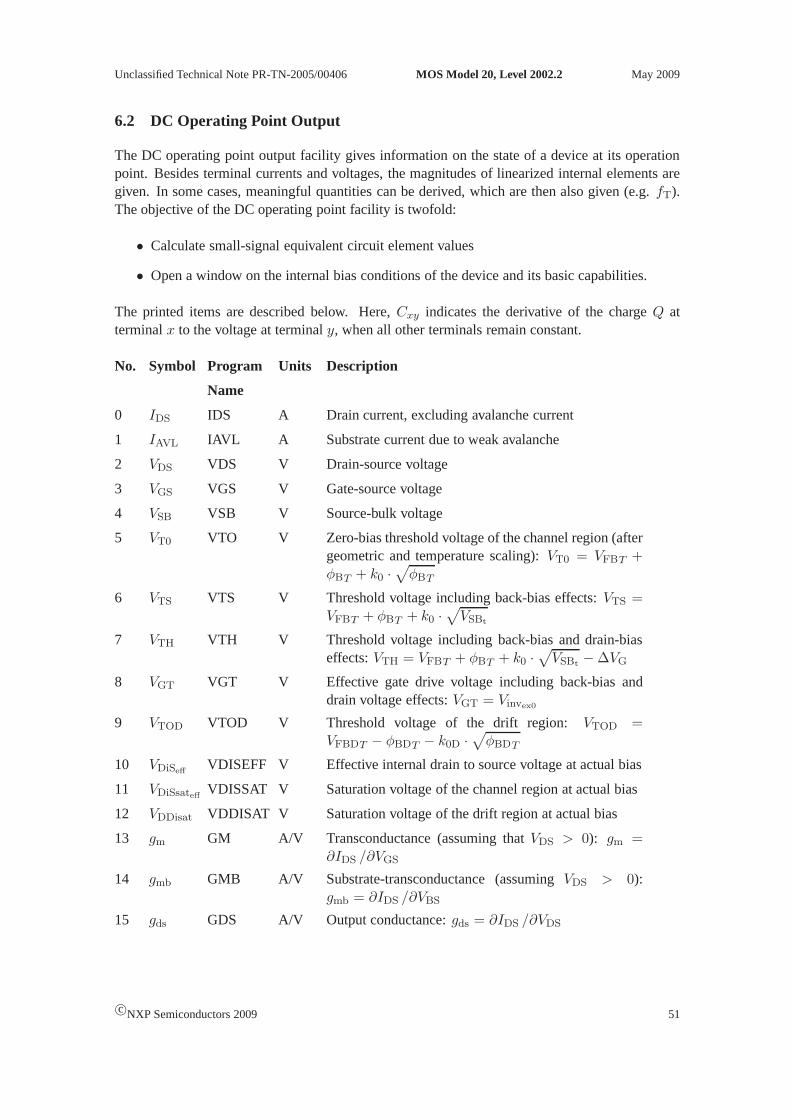
Unclassified Technical Note PR-TN-2005/00406 MOS Model 20, Level 2002.2 May 2009
6.2 DC Operating Point Output
The DC operating point output facility gives information onthe state of a device at its operationpoint. Besides terminal currents and voltages, the magnitudes of linearized internal elements aregiven. In some cases, meaningful quantities can be derived,which are then also given (e.g.fT).The objective of the DC operating point facility is twofold:
• Calculate small-signal equivalent circuit element values
• Open a window on the internal bias conditions of the device and its basic capabilities.
The printed items are described below. Here,Cxy indicates the derivative of the chargeQ atterminalx to the voltage at terminaly, when all other terminals remain constant.
No. Symbol Program Units Description
Name
0 IDS IDS A Drain current, excluding avalanche current
1 IAVL IAVL A Substrate current due to weak avalanche
2 VDS VDS V Drain-source voltage
3 VGS VGS V Gate-source voltage
4 VSB VSB V Source-bulk voltage
5 VT0 VTO V Zero-bias threshold voltage of the channel region (aftergeometric and temperature scaling):VT0 = VFBT +φBT + k0 ·
√
φBT
6 VTS VTS V Threshold voltage including back-bias effects:VTS =VFBT + φBT + k0 ·
√
VSBt
7 VTH VTH V Threshold voltage including back-bias and drain-biaseffects:VTH = VFBT + φBT + k0 ·
√
VSBt− ∆VG
8 VGT VGT V Effective gate drive voltage including back-bias anddrain voltage effects:VGT = Vinvex0
9 VTOD VTOD V Threshold voltage of the drift region:VTOD =VFBDT − φBDT − k0D ·
√
φBDT
10 VDiSeffVDISEFF V Effective internal drain to source voltage at actual bias
11 VDiSsateff VDISSAT V Saturation voltage of the channel region at actualbias
12 VDDisat VDDISAT V Saturation voltage of the drift region at actual bias
13 gm GM A/V Transconductance (assuming thatVDS > 0): gm =∂IDS /∂VGS
14 gmb GMB A/V Substrate-transconductance (assumingVDS > 0):gmb = ∂IDS /∂VBS
15 gds GDS A/V Output conductance:gds = ∂IDS /∂VDS
c©NXP Semiconductors 2009 51

May 2009 MOS Model 20, Level 2002.2 Unclassified Technical Note PR-TN-2005/00406
No. Symbol Program Unit Description
Name
16 CDD CDD F CDD = ∂QD /∂VDS
17 CDG CDG F CDG = −∂QD /∂VGS
18 CDS CDS F CDS = CDD − CDG − CDB
19 CDB CDB F CDB = ∂QD /∂VSB
20 CGD CGD F CGD = −∂QG /∂VDS
21 CGG CGG F CGG = ∂QG /∂VGS
22 CGS CGS F CGS = CGG − CGD − CGB
23 CGB CGB F CGB = ∂QG /∂VSB
24 CSD CSD F CSD = −∂QS /∂VDS
25 CSG CSG F CSG = −∂QS /∂VGS
26 CSS CSS F CSS = CSG + CSD + CSB
27 CSB CSB F CSB = ∂QS /∂VSB
28 CBD CBD F CBD = −∂QB /∂VDS
29 CBG CBG F CBG = −∂QB /∂VGS
30 CBS CBS F CBS = CBB − CBD − CBG
31 CBB CBB F CBB = −∂QB /∂VSB
32 WE WEFF m Effective channel region width for geometrical model
33 WED WDEFF m Effective drift region width for geometrical model
34 u U - Transistor gain:u = gm /gds
35 Rout ROUT Ω Small-signal output resistance:Rout = 1/gds
36 VEarly VEARLY V Equivalent Early voltage:VEarly = |IDS| /gds
37 βeff BEFF A/V2 Gain factor:βeff = 2 · |IDS| /V 2invex0
38 fT FUG Hz Unity gain frequency at actual bias:fT =gm
2 · π · (CGG +CGSO + CGDO)
39 gmchGMMOS A/V Transconductance of the channel region
40√
SVGthSQRTSFW V/
√Hz Input-referred RMS thermal noise voltage density:
√
SVGth=√
SDth/gmch
41√
SVGflSQRTSFF V/
√Hz Input-referred RMS flicker noise voltage density at 1
kHz:√
SVGfl=√
SDfl[1kHz] /gmch
42 fknee FKNEE Hz Cross-over frequency above which thermal noise isdominant:fknee = 1Hz · SDfl
[1Hz] /SDth
52 c©NXP Semiconductors 2009

Unclassified Technical Note PR-TN-2005/00406 MOS Model 20, Level 2002.2 May 2009
References
[1] http://www.nxp.com/models/
[2] N. D’ Halleweyn,Modelling and Characterisation of Silicon-On-Insulator Lateral Dou-ble Diffused MOSFETs for Analogue Circuit Simulation, Ph.D. Thesis, University ofSouthampton, 2001.
[3] R. van Langevelde and F.M. Klaassen,An Explicit Surface-Potential Based MOSFETModel for Circuit Simulation, J. Solid-State Electronics, Vol. 44, pp. 409–418, 2000.
[4] R. van Langevelde, A.J. Scholten, and D.B.M. Klaassen,MOS Model 11, level1101, Philips Research Unclassified Report, NL-UR 2002/802, December 2002 (seehttp://www.nxp.com/models/).
[5] A.C.T. Aarts and R. van Langevelde,A Robust and Physically Based Compact SOI-LDMOS Model, Proc. ESSDERC, pp. 455–458, 2002.
[6] D.E. Ward and R.W. Dutton,A Charge-Oriented Model for MOS Transistor Capaci-tances, J. Solid-State Electronics, Vol. 13, No. 5, pp. 703–708, 1978.
[7] A.C.T. Aarts, M.J. Swanenberg, and W.J. Kloosterman,Modelling of High-VoltageSOI-LDMOS Transistors including Self-Heating, Proc. SISPAD, Springer, pp. 246–249,2001.
[8] A.C.T. Aarts, N. D’Halleweyn, and R. van Langevelde,A Surface-Potential-Based High-Voltage Compact LDMOS Transistor Model, IEEE Trans. Electron Devices, Vol. 52,No. 5, pp. 999–1007, 2005.
c©NXP Semiconductors 2009 53

May 2009 MOS Model 20, Level 2002.2 Unclassified Technical Note PR-TN-2005/00406
54 c©NXP Semiconductors 2009

Unclassified Technical Note PR-TN-2005/00406 MOS Model 20, Level 2002.2 May 2009
A Auxiliary Functions
The hyp function:
hyp[x; ǫ] =1
2·(
x +√
x2 + 4 · ǫ2)
(A.1)
The hypm function:
hypm[x, y;m] =x · y
(x2·m + y2·m)1/(2·m)(A.2)
c©NXP Semiconductors 2009 55