
MOS CCDs for the Wide Field Imager on the XEUS Spacecraft
12
MOS CCDs for the Wide Field Imager on the XEUS Spacecraft A.D. Holland †a , C. Castelli a , I Hutchinson a , D.R. Smith a , J. Calafell a , P. Pool b , D. Burt b , R. Ambrosi c and M. French d a e2v centre for electronic imaging, Brunel University, Uxbridge, UB8 3PH, UK b e2v technologies, Waterhouse Lane, Chelmsford, CM1 2QU, UK c Space Research Centre, University of Leicester, University Road, Leicester, LE1 7RH, UK d Instrumentation Division, CCLRC, Chilton, Oxford, OX11 0QX, UK ABSTRACT In recent years the XEUS mission concept has evolved and has been the subject of several industrial studies. The mission concept has now matured to the point that it could be proposed for a Phase A study and subsequent flight programme. The key feature of XEUS will be its X-ray optic with collecting area ~30-100x that of XMM. The mission is envisaged at an orbit around the L2 point in space, and is formed from two spacecraft; one for the mirrors, and the other for the focal plane detectors. With a focal length of 50m, the plate scale of the optic is 6.5x that of XMM, which using existing focal plane technology will reduce the effective field of view to a few arc minutes. Cryogenic instrumentation, with detector sizes of a few mm can only be used for narrow field studies of target objects, and a wide field instrument is under consideration using a DEPFET pixel array to image out to a diameter of 5 arcminutes, requiring an array of dimension 70mm. It is envisaged to extend this field of view possibly out to 15 arcminutes through the use of an outer detection ring comprised of MOS CCDs Keywords: X-ray spectroscopy, x-ray imaging, CCD, focal plane array 1. INTRODUCTION The X-ray Evolving Universe Spectroscopy (XEUS) [1] mission represents a potential follow-on mission to the ESA XMM (Newton) cornerstone which has been operating successfully for the last 5 years. The XEUS mission was originally studies as part of the utilization of the International Space Station (ISS), however, has recently become de-coupled from ISS activities and is now a stand-alone mission destined for an L2 orbit. The primary aim of XEUS is to study the astrophysics of some of the most distant and hence youngest known discrete objects in the universe. The specific scientific issues, which XEUS aims to address, can be summarized as follows: • to measure the spectra of objects with a redshift z >4 at flux levels below 10 -18 erg cm -2 s -1 , this is 1000 times fainter than that achievable with XMM • to determine from the X-ray spectral lines the redshift and thus age of these objects and to establish the cosmological evolution of matter in the early universe. Achieving the scientific performance for collecting area and hard X-ray response necessitates a separate mirror (MSC) and detector spacecraft (DSC). The DSC would need to maintain itself at the focus of the X-ray optic to within a cube of dimension 2x2x2 mm 3 . This configuration with two spacecraft makes the instruments sensitive to stray light, since no closed structure exists between the mirror and the focal plane. This means that the mirror and detector spacecraft rely on very effective baffling at unit level. The instrument requirements for XEUS have been discussed earlier [2]. Here we outline an initial design concept for an extension to the field of view of the wide field imager (E-WFI) and discuss both the demanding instrument requirements imposed by the proposed X-ray optic, together with the new developments in MOS CCD technology which could be used to provide additional science benefits for the mission. † Corresponding author : [email protected], Tel +44 1895 266 516, Fax +44 1895 269 773
Transcript of MOS CCDs for the Wide Field Imager on the XEUS Spacecraft

MOS CCDs for the Wide Field Imager on the XEUS Spacecraft
A.D. Holland †a, C. Castellia, I Hutchinson a, D.R. Smitha, J. Calafell a, P. Poolb, D. Burt b, R. Ambrosic and M. French d
a e2v centre for electronic imaging, Brunel University, Uxbridge, UB8 3PH, UK b e2v technologies, Waterhouse Lane, Chelmsford, CM1 2QU, UK
c Space Research Centre, University of Leicester, University Road, Leicester, LE1 7RH, UK d Instrumentation Division, CCLRC, Chilton, Oxford, OX11 0QX, UK
ABSTRACT In recent years the XEUS mission concept has evolved and has been the subject of several industrial studies. The mission concept has now matured to the point that it could be proposed for a Phase A study and subsequent flight programme. The key feature of XEUS will be its X-ray optic with collecting area ~30-100x that of XMM. The mission is envisaged at an orbit around the L2 point in space, and is formed from two spacecraft; one for the mirrors, and the other for the focal plane detectors. With a focal length of 50m, the plate scale of the optic is 6.5x that of XMM, which using existing focal plane technology will reduce the effective field of view to a few arc minutes. Cryogenic instrumentation, with detector sizes of a few mm can only be used for narrow field studies of target objects, and a wide field instrument is under consideration using a DEPFET pixel array to image out to a diameter of 5 arcminutes, requiring an array of dimension 70mm. It is envisaged to extend this field of view possibly out to 15 arcminutes through the use of an outer detection ring comprised of MOS CCDs Keywords: X-ray spectroscopy, x-ray imaging, CCD, focal plane array
1. INTRODUCTION The X-ray Evolving Universe Spectroscopy (XEUS) [1] mission represents a potential follow-on mission to the ESA XMM (Newton) cornerstone which has been operating successfully for the last 5 years. The XEUS mission was originally studies as part of the utilization of the International Space Station (ISS), however, has recently become de-coupled from ISS activities and is now a stand-alone mission destined for an L2 orbit. The primary aim of XEUS is to study the astrophysics of some of the most distant and hence youngest known discrete objects in the universe. The specific scientific issues, which XEUS aims to address, can be summarized as follows:
• to measure the spectra of objects with a redshift z >4 at flux levels below 10-18 erg cm-2 s-1 , this is 1000 times fainter than that achievable with XMM
• to determine from the X-ray spectral lines the redshift and thus age of these objects and to establish the cosmological evolution of matter in the early universe.
Achieving the scientific performance for collecting area and hard X-ray response necessitates a separate mirror (MSC) and detector spacecraft (DSC). The DSC would need to maintain itself at the focus of the X-ray optic to within a cube of dimension 2x2x2 mm3. This configuration with two spacecraft makes the instruments sensitive to stray light, since no closed structure exists between the mirror and the focal plane. This means that the mirror and detector spacecraft rely on very effective baffling at unit level. The instrument requirements for XEUS have been discussed earlier [2]. Here we outline an initial design concept for an extension to the field of view of the wide field imager (E-WFI) and discuss both the demanding instrument requirements imposed by the proposed X-ray optic, together with the new developments in MOS CCD technology which could be used to provide additional science benefits for the mission.
† Corresponding author : [email protected], Tel +44 1895 266 516, Fax +44 1895 269 773

The effective area and hard X-ray performance of the mirror, combined with the 3 arcsecond PSF requirement, leads to a telescope focal length of 50m. This necessitates a separate mirror (MSC) and detector spacecraft (DSC), both orbiting around the L2 point. The increase in focal length, compared to that of XMM, results in a corresponding increase in the plate scale of 6.7x which drives up the size of the focal plane detectors. Whilst the XMM field of view extends to a 30 arcminute diameter, the XEUS baseline is currently only 5 arcminutes, with a target of achieving 10 arcminutes. Here we discuss CCD technology designed to increase the field of view coverage of the main imager, the WFI (wide field imager) so that it can better utilize the field of view of the X-ray optic, possibly covering a >15 arcminute diameter field of view (FOV). This additional imaging ‘ring’ has been called the E-WFI (extended-wide field imager). Figure 1 gives an image taken from XMM showing a typical cluster and has superimposed the minimum XEUS requirement baseline of a 5x5 arcminute FOV. This inner FOV would be covered using a high-throughput DEPFET array whose size of 70x70 mm2 exceeds that of the XMM EPIC pn focal plane. Shown also is the 15x15 arcminute FOV possible using an outer mosaic of large area CCDs. The planned cryognic narrow field instruments, will only have sufficient field of view to sample point sources and their local background.
E-WFI
Figure 1 : Typical image of a cluster taken with XMM superimposed with a 5’x5’ field of view for the baseline WFI, and a 15’x15’ field of view for the E-WFI
2. THE XEUS WIDE FIELD IMAGER
The concept for the WFI is given in Figure 2 and depicts the outline of the baseline WFI comprising a Depleted P-channel Field Effect Transistor (DEPFET) array of size up to 70x70 mm2 [3] below which is located a hard X-ray CZT pixel array detector which detects the hard X-rays between 10-50 keV which penetrate the DEPFET array [4]. The outer field of the focal plane is covered using a mosaic of large area MOS CCDs. The combination of depth of focus and focal surface curvature enable the combined WFI to be constructed on multiple layers without significantly degrading the half energy width (HEW) of the PSF. The performance targets for the combined WFI instrument are given in Table 1. The resulting combined instrument may therefore be treated as three separate units which can each be separately developed and tested, before being integrated. Whilst the interfaces for such an instrument can be defined relatively early, in addition in the medium-term, the potential cross-talk between the differing detector technologies and their support electronics will also be investigated.

Figure 2 : Concept design for the combined WFI, including the central DEPFET array, the extended wide field imager, plus hard X-ray imager below the DEPFET array.
Table 1 : The Combined WFI and E-WFI instrument parameters
Parameter WFI E-WFI Detector Type DEPFET Array MOS CCD Field Coverage (diameter) 5 arcmin 5-15 arcmin Number of pixels 1000x1000 Multiple modules Pixel size 75µm 75 µm Energy resolution (eV) 125 eV @ 6 keV 125 eV @ 6 keV Detection Efficiency (%) 100 % @ 6 keV Depends on Si thickness Time Resolution <5 ms 20 ms Operating temperature 180-220 K 185 K
At the current time the exact layout of the WFI has not been finalised. The requirements placed on the MOS CCDs forming the E-WFI at this early stage in the instrument definition are fairly broad but comprise the following
• Large unit area to minimise the number of detectors in the resulting mosaic array and thereby the support electronics
• Pixel size <150 μm to allow over sampling of the optic PSF • Able to handle a photon throughput in excess of 1000/s/psf with low pileup • Sensitivity optimised over the 0.3-2keV band taking account of instrument background (since most photons are
below the gold M-edges from the effective area and the prime aim is to detect faint, high redshift objects, e.g. z=2-3 would contain emission from iron lines in the range 2.2-1.6 keV)
• High detection efficiency over the 0.3-10 keV band – but consistent with the point above • Radiation hard over the mission duration
A design study is about to commence which will formulate the optimum layout of the CCD for XEUS taking account of the diverse requirements. The next section describes the technology developments in CCDs.

3. CCD DEVELOPMENTS FOR THE EXTENDED WIDE FIELD IMAGER 3.1 Large Area Mosaics
Figure 3 : CFHT mosaic on Hawaii formed from a close-butted array of e2v CCD42-90 back-illuminated sensors
Figure 4 : New generation of large area CCDs formed using 2D stitching showing the ESA Gaia AF CCD together with a wafer of WFC3
detectors A large area mosaic is ideally formed from a mosaic focal plane array (FPS) of a small number of large area CCDs. As well as being simpler to procure and assemble, this also reduces the complexity of the drive and processing electronics. Packaging technology has now developed such that large area mosaic arrays such as that shown in Figure 3 for CFHT are becoming routine. In these arrays, the CCD packaging has developed pseudo-2D butting with close butting on 3 sides and slightly relaxed butting on the 4th side for electrical connections. Figure 4 shows ESA’s Gaia AF (astrometric field) CCD which is one of the largest CCDs in production [5]. This device was manufactured using 2D photolithographic stitching to produce only two senors per 5” wafer. The Gaia mission, to be flown in 2011, will require >100 such devices for its astrometric focal plane in a close-butted array. The concept therefore of a large mosaic array of flight qualified CCDs will have been adequately demonstrated prior to the XEUS mission and will therefore be a relatively low development risk.

Whilst very large area devices such as the Gaia AF CCD reduce the number of sensors required to cover the field of view, they do have two drawbacks; the impact of radiation damage scales with the detector area, but more importantly, for high frame rate applications using conventional polysilicon electrodes, the maximum clocking speed is proportional to the square of the device width. Therefore the parallel shift time period may be several 10’s of μs which can impact on “out of time” events or image smear resulting in the XEUS E-WFI instrument favouring a narrow CCD geometry such as that indicated in Figure 2. This has the added advantage of providing 2-3 devices per wafer which may yield a greater number of devices per batch. In designing a focal plane mosaic, particularly one where overall cost, or value for money, has to be considered, a detailed model of the optimum solution will have to be performed. Factors affecting the total cost of a focal plane array are
• Yield, and hence price, per detector unit • Number of detectors forming the focal plane • Number of output nodes impacting video processing units and drive electronics • Total system calibration effort (where the effort strongly depends on number of detectors and readout nodes)
This tradeoff will be performed over the coming 6 months as an input to the CCD design activity, resulting in a new WFI baseline being adopted. Since the project has not entered its flight phase, further modifications to the CCD and focal plane layout formats will be possible before being finalized. 3.2 High Sensitivity, Low Background CCDs
Figure 5 : a) XMM MOS camera background spectra for instrument (lower line) and instrument+sky (upper line) and b) Comparison of instrument background spectra using the closed filter position in XMM’s MOS and pn cameras. The pn detector background intensity (300 μm-thick) is about 2.8x greater than MOS detector (~35 μm active)
One of the main roles of the WFI on XEUS will be to perform targeted observations on known sources. Therefore it is essential that the central field detector has a high efficiency over a broad bandpass, particularly over the 5-10 keV region to perform Fe-line science and to determine the high energy tail of the sources. Outside of the central region (and off-target), is where the majority of new sources will be detected. In the outer detectors, optimisation for serendipity is paramount rather than broad band-pass. In the E-WFI, to optimise the performance for serendipitous work one must not simply maximise the detector efficiency, but must consider the total instrument sensitivity, including instrument background. Figure 5 gives the result of background analysis in XMM for a) the MOS camera (~35 μm active layer) giving both internal instrument background taken from the
regions of the detectors outside the field of view defined by the filters, and the sky background+internal. The results show continuum spectra with elemental fluorescence lines arising from Al K, Si K, Au M and L, Fe K Cr K etc. From this data, plus analysis of similar data from the pn-CCD camera, we conclude that the XMM EPIC backgrounds in both camera types are dominated by the diffuse X-ray background below ~5keV and by un-rejected particles at higher energies. Figure 5 b) gives a comparison of the true instrument background for pn (upper) and MOS (lower) cameras indicating that the background in the 300 μm-thick detector is typically a factor 2.8x that measured in the thinner detector with 35 μm active layer [6]. It is to some degree ironic then, that whilst efforts have been made over the last 20 years to increase the high energy quantum efficiency (QE) of CCDs for the direct detection of X-rays, using high resistivity/deep depletion material, that these same measures have also increased the instrument background due largely to Compton interactions in the detector. In a purely Compton model, the background would scale in proportion to detector thickness, and the EPIC pn background should be ~8x greater than that of the MOS camera. The measured performance in the two camera types indicates a sub-linear relationship with detector thickness indicating other processes at work. A detailed analysis of the background for XEUS is therefore to be performed leading to a recommendation of the optimal detection thickness for the MOS CCD sensors to provide the highest sensitivity for serendipitous sources. This will need to take into account the performance of the optics, together with an estimate of the resolved component of the X-ray background. 3.3 Pixel size
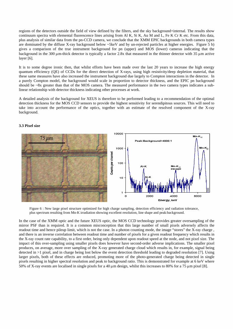
Figure 6 : New large pixel structure optimized for high charge sampling, detection efficiency and radiation tolerance, plus spectrum resulting from Mn-K irradiation showing excellent resolution, line shape and peak:background.
In the case of the XMM optic and the future XEUS optic, the MOS CCD technology provides greater oversampling of the mirror PSF than is required. It is a common misconception that this large number of small pixels adversely affects the readout time and hence pileup limit, which is not the case. In a photon counting mode, the image “stores” the X-ray charge , and there is an inverse correlation between readout time and number of pixels for a given readout frequency which results in the X-ray count rate capability, to a first order, being only dependent upon readout speed at the node, and not pixel size. The impact of this over-sampling using smaller pixels does however have second-order adverse implications. The smaller pixel produces, on average, more over sampling of the X-ray generated charge cloud which results in, for example, signal being detected in >1 pixel, and in charge being lost below the event detection threshold leading to degraded resolution [7]. Using larger pixels, both of these effects are reduced, promoting more of the photo-generated charge being detected in single pixels resulting in higher spectral resolution and peak to background ratio. This is demonstrated for example at 6 keV where 50% of X-ray events are localised in single pixels for a 40 μm design, whilst this increases to 80% for a 75 μm pixel [8].
Conventional CCDs have pixel sizes of between 9-27 μm, with the smaller size used for high spatial resolution applications, such as optical astronomy, and the larger for less demanding imaging applications such as X-ray optics or radiography. All CCDs must be designed with high charge transfer efficiency (CTE) as a goal. Good CTE in a CCD is largely mediated through the drift, or fringing fields, between adjacent phases which promote transfer of all electrons within a short transfer time. At the larger pixel sizes, the upper limit of the pixel size is limited by the transfer time across a wide electrode with a decreasing drift field aiding the transfer. In the JET-X CCD, the largest electrode was defined with 17 μm width for this reason. The new pixel structure which has been designed is shown in Figure 6 and has been developed from the XMM EPIC open electrode CCD [9] where transfer across the wide phase is assisted by a static drift field built into the electrode shape [10]. In the new design, the structure has been developed with pixels of dimension 75 and 100 μm manufactured. Since charge is stored in the nodes of the electrodes, the new design should result in improved radiation hardness by a factor ~3x that of the XMM EPIC detectors, whilst providing the added benefits of improved detection efficiency (later sections) and good charge cloud sampling. The measured X-ray spectrum using Mn fluorescence X-rays is also given in Figure 6 showing that the detector works with excellent CTE and resolution. In practice, therefore, we have demonstrated that MOS CCDs can be manufactured having pixels of any size up to 100 μm, with the possibility of extending this size up to 150 μm if required for flight. 3.4 High Energy Efficiency It has long been known that to good detection for the higher energies requires the use of deep depletion devices, manufactured on high resistivity silicon [11]. When using CCDs manufactured on high resistivity bulk silicon, the conventional CCD may possess a depletion of between 35-70 μm resulting in an efficiency at 10 keV of 22-42%. The remainder of the bulk silicon, with thickness ~500 μm, possesses low charge collection efficiency (CCE) and is not useful for spectroscopy. We have investigated depleting a greater proportion of this bulk silicon. The depletion layer depth can be increased by a higher channel potential or higher biases, however these methods are limited by increased bright defect generation and by device breakdown. The preferable method of obtaining increased depletion depth is to lower the substrate doping concentration, i.e. use higher resistivity silicon. Current missions, such as EPIC, use MOS devices with much higher resistivity silicon (2 - 10 kΩ), resulting in depletion depths greater than 30 µm (~25 % QE at 10 keV) [10] with standard operating voltages. Earlier in the development phase of EPIC, CCDs were manufactured on 8 kΩ-cm bulk silicon and achieved a depletion depth of ~ 65 µm.
As a comparison, the expected value of depletion depth was calculated from the simplified formula for the depletion depth, D, using the equation;
a
Si
eNV
Dε2
= (1)
where V is the area-weighted average gate voltage applied between the pixel and the substrate bias, and Na is the substrate doping concentration. The average applied gate voltage must be calculated by performing an area-weighted average over the pixel considering;
• Channel parameter for buried channel and 0V for surface channel areas • High-biased phases and low-biased phases, where maximum depletion arises from biasing 2 phases high during
integration, and designing unequal gate widths, with the low bias applied to the narrowest • As above during readout, weighted for relative times • Substrate Bias
which lead to the predicted depletion depths as a function of substrate bias using normal clock voltages shown in Table 2.

Table 2 : Predicted depletion depths Period Vss=+6V Vss=-8.7V Vss=-54V
During Integration 71 μm 121 μm 235 μm During Readout 55 μm 113 μm 210 μm
Average (tint=2×tread) 66 μm 118 μm 226 μm
Figure 7 : Theoretical depletion depth vs. averaged pixel-substrate bias for a CCD manufactured on 8 kΩcm silicon, together with values (lines) measured during the course of this work
Figure 7 shows the average depletion depth as a function of averaged pixel-to-substrate bias for a CCD manufactured on 8 kΩcm silicon, indicating that a bias voltage exceeding 100V is required to deplete to a depth >200 μm. The initial experiments have shown that a significant increase in the depletion depth can be achieved by the use of negative Vss values whilst maintaining good cosmetic performance. This type of increased efficiency could be implemented for the XEUS E-WFI. Further to this it could be possible to use 12,000 Ωcm n-type silicon with p-type buried channel (boron doped) to give a 3 increase in the depletion depth to >350 μm if required. The feasibility of p-channel CCDs has already been demonstrated by e2v technologies and is currently under development. 3.5 Low Energy Efficiency There are three established methods for improving the low energy efficiency of CCDs, namely; thin electrode [12,13], some form of virtual phase [14] which includes open electrode technology [9] and back illumination [16]. The last two of these approaches incorporate pinning implants with associated low field regions at the entrance window. Carrier trapping in these low field regions can then degrade the low energy spectroscopy possible with these devices. On the other hand, with the thin electrode technology, for photons penetrating the entrance window (electrodes and dielectric in this case) the charge is generated in a high field region with very high CCE leading to the best spectral resolution. Thin electrode devices have resulted in spectral resolutions at carbon (277eV) of <40 eV full width at half maximum (FWHM) [6]. It is for this reason that we are currently developing the thin electrode technique beyond that currently demonstrated for JET-X [15] or the original Cubic CCDs [13] which possessed electrodes of 170 nm down to a thickness of 40 nm for the largest of the of the four electrodes shown in Figure 6. In the CCDs for JET-X and Cubic, the thin electrode limit of 170 nm was determined by the rapid increase in polysilicon sheet resistance with decreasing sheet thickness. This increase in resistance occurs due to the grain boundaries created by the growth of grains in the deposited ploysilicon during the subsequent thermal processing. The development of thinner electrode structures required process experimentation to be performed on the grown polysilicon layers, and their doping.

Figure 8 : a) SEM image of a CCD electrode structure showing the granularity of the polysilicon electrodes. b) SEM image of resistor test structures used to develop the 40 nm thin gate process.
Figure 9 : Quantum Efficiency of proposed new ultra-thin electrode structure using 40nm gate dielectric layers together with the pixel structure shown in Figure 3
Figure 8 a) depicts an SEM image of a conventional polysilicon electrode structure and shows the granularity of the 500nm layers. Experimentation in the layer thickness, its doping, and the subsequent thermal processing, enabled layers to be grown on test structures down to a thickness of 40nm. Figure 8 b) shows a resistor structure used in the trials to evaluate the sheet resistance of the grown layers. These trials demonstrated that 40 nm polysilicon layers could be fabricated and progressed through the subsequent device thermal processing. To utilise the advantage in detection efficiency using gate structures as thin as 40 nm, also requires thin dielectric layers, where the silicon oxide and nitride layers are reduced from the standard 850 nm to 40 nm, and the removal of the 500nm VAPOX layer over the thin poly regions. Both of these processes have already been demonstrated in the past. With thin gate dielectric layers of only 40nm, the resulting low-energy detection efficiency is shown in Figure 9, together with the efficiency of the JET-X detectors and a standard front-illuminated device. The major improvement in detection efficiency arises from the large area of thin electrode made possible by the pixel structure. The detection efficiency at 300eV of ~30% is the same as that measured for the open electrode CCDs used on XMM EPIC.

3.6 High Count Rate The XMM EPIC MOS focal plane was designed to perform imaging X-ray spectroscopy on sources of up to the mCrab level on the whole field. The CCD operates with a full frame readout time of 2.6s, and this produces a maximum X-ray throughput of ~5 counts per second in the PSF. It should be noted that this limit depends upon the following;
• Acceptable pileup percentage (<2% for above limit) • Frame time (or window time for reduced window) • Pixel size.
The important feature for pileup is the frame time-pixel size product. In XEUS, the proposed DEPFET array will cover the field <5” and will be capable of performing imaging spectroscopy on brighter sources. The E-WFI array, whose primary role is to detect serendipitous sources, need only handle sources of brightness up to the mCrab level. Since the optic of XEUS will be up to a maximum 100x the area of XMM, a source of mCrab brightness will produce approximately 1000 X-rays/s in the PSF (~1mm FWHM). This increase in X-ray throughput can be achieved by operating the detectors faster at up to 1 Mpix/s (~170kHz for EPIC), and providing a so-called multi-tap architecture, with up to 16 nodes. With up to 16 readout nodes per CCD and up to 16 CCDs in the focal plane, the use of conventional electronics to read-out the detectors is not appropriate and would lead to an unduly complex system. Whilst the CCDs can be clocked in parallel, with some degree of commonality, the data streams must be separate up to the X-ray event processing. We have therefore embarked upon a development to investigate the use of analogue ASICs to perform the function of analogue signal processing and noise reduction. This development is described in detail in reference [16]. It has been shown that a total system noise of between 6-10 electrons has been realised to-date and improvements are underway to reduce this to the XEUS MOS CCD noise specification of 5 electrons rms. In addition, the first design of multi-channel CDS ASIC has been developed and is shown in Figure 10.
Figure 10 : Schematic of the 4-channel CDS ASIC together with photomicrograph and hybrid module constructed using the 2 channel ASIC version.
Figure 10 gives a schematic of the now 4-channel CDS ASIC. This ASIC has an internal 10-bit DAC for offset adjust which can be used in a “Gatti” technique to eliminate differential non-linearity in ADCs which can be a problem for X-ray spectroscopy. In addition, each channel has a 7-bit programmable gain, which could be used to tweak the responses of the different channels in a flight configuration. Here we designed the 4-channel system as a prototype for the XEUS application. The CDS unit cell can be replicated to produce an 8 or 16-channel CDS version. Future iterations will have additional gain at the input stage, and may include either analogue multiplexing, or a 12 bit ADC to provide a digital output.

The decision between analogue or digital multiplexing, on or off-chip ADCs, has not yet been made, however, it is likely that the project may use conventional ADCs since these are commercially available items
4. POWER DISSIPATION AND COOLING Table 3 : Clocking Power Dissipation
Parameter 30 mm-wide CCD 60 mm-wide CCD Clock Voltage 10V 5V 10V 5V Image + Store Power 658 mW 165 mW 470 mW 117 mW Serial Register Power 50 mW 17 mW 100 mW 25 mW Total clock dissipation 710 mW 180 mW 570 mW 140 mW
We have discussed how the focal plane array may be constructed out of a large number of relatively smaller detectors, or from fewer large area ones. The use of large area detectors is not favoured either for frame rate of radiation damage reasons, but could significantly simplify the E-WFI total system. Table 3 gives the clocking power dissipation for two CCD width options (assuming a 50mm length) and for two clock voltages. As can be seen from the table, since the clocking dissipation is proportional to V2 at the high rates envisaged for XEUS the use of standard image clock voltage swings of 10V results in high power dissipation. For XEUS it is more appropriate to use reduced 5V clocks to limit the total dissipation. Table 4 : Total CCD Module Power Dissipation
Parameter 8 Node 16 node Clock Dissipation (5V) 180 mW 140 mW Radiative coupling 18 mW 18 mW Amplifier Dissipation 160 mW 320 mW ASIC Dissipation 400 mW 750 mW Total dissipation / module 748 mW 1228 mW Total FPA dissipation – 16 CCDs 12 W 20 W Radiator Size (+50%, 0.8) 0.35 m2 0.6 m2
Table 4 gives a calculation for the total module dissipation for a 50x30 mm2 image area, with both 8 and 16 readout nodes. The dissipation of a typical CCD output node is 20 mW, and the module power therefore is strongly affected by the number of nodes. The table also indicates the typical size of a radiator required assuming passive cooling to cool a focal plane array of 16 such modules. This calculation assumes an additional 50% parasitic loading and a radiator end of life emissivity of 0.8, both of these figures are conservative. The results show that an 8 node CCD module results in a total radiator requirement just over 0.3 m2 which is comparable to that of XMM EPIC, whilst the 16 node solution would require a radiator of twice that area. If the XEUS mission were to require the additional throughput provided by 16 nodes per module, then a more efficient cooling solution could be achieved by cooling the module to -30oC using a passive radiator, and using a thermo electric cooler (TEC) to locally cool the CCD silicon only, down to the required operating temperature of -90oC. This active cooling solution would again only require a passive radiator of 0.3 m2 which is considered a modest resource requirement.
5. CONCLUSIONS We have described here the initial concept for the extended wide field imager for the XEUS WFI instrument. Several improvements to the detector technology have occurred since the design of the XMM EPIC MOS CCDs which will improve the instrument performance. At the current timing in the project, the design detail for the WFI instrument is just about to go through a major overhaul leading to the production of a prototype module. We have detailed preliminary design concepts which can be developed into the XEUS module demonstrator for the focal plane mosaic concept. This refinement will crystallise a new sensor size and number of CCDs, number of readout nodes per CCD, and optimal module design and

cooling. We have shown that the focal plane array, which will be much larger in surface area than XMM EPIC can be achieved using modest spacecraft resources in terms of power, and focal plane cooling.
ACKNOWLEDGEMENTS The CCD development work is supported by the United Kingdom’s Particle Physics and Astronomy Research Council (PPARC). The authors would like to thank David Burt and Ralph Holtom of e2v technologies for support and helpful comments over the years.
REFERENCES 1. M. Bavdaz et al, “X-ray evolving universe spectroscopy mission (XEUS)”, Proc SPIE 3766 (1999) 2. P.A. deKorte et al, "X-ray evolving universe spectroscopy mission (XEUS): narrow-field imaging high-resolution
spectrometer: II (1 to 10 keV)", Proc. SPIE 3766 (1999) 152 3. P. Holl et al, “Active Pixel Matrix for X-ray Satellite Missions”, IEEE Trans. on Nucl. Sci. 47 No 4 (2000) 4. L. Strueder et al., “Imaging spectrometers for future X-ray missions”, Proc. SPIE 4497 (2001) 5. A.D.T. Short et al, “Gaia astrometric CCDs and focal plane”, Proc SPIE 5902 (2005) in press 6. A.D. Holland, “X-ray Spectroscopy using MOS CCDs”, NIM A337 (1996) 334 7. K.J. McCarthy, A. Owens, A.D. Holland and A. Wells, “Modelling the X-ray response of CCDs”, NIM A362 (1995)
538-546 8. R.M Ambrosi, A.D. Holland, K. Mukerjee, A. Keay, M.J.L. Turner, A. Abbey, I.B. Hutchinson, T.J.R. Ashton, A.
Beardmore, A.D.T. Short, P. Pool, D.J. Burt and D. Vernon, “Next Generation detectors for X-ray astronomy”, Proc. SPIE, 5501 (2004) 11-22
9. A. D. Holland, M. J. Turner, A. F. Abbey et al, “MOS CCDs for the EPIC on XMM”, Proc. SPIE 2808, pp. 414-420 (1996).
10. A.D.T. Short, A. Keay and M. J. L. Turner, "Performance of the XMM EPIC MOS CCD Detectors", Proc. SPIE (1998) 11. D.H. Lumb and A.D. Holland, “X-ray imaging spectroscopy with EEV CCDs”, Proc SPIE 982 pp. 116 (1988) 12. A.D. Holland, M.J.L. Turner, A. Wells and D.J. Burt, “CCDs on high resistivity bulk silicon for X-ray spectroscopy on
XMM”, ESA Publications, SP-356 (1992) 321-324 13. M.A. Skinner et al, “CUBIC: Laboratory Testing of Thin Poly CCDs”', Proc. SPIE 2006 (1993) 258-264 14. J. Janesick, “Open-pinned phase CCD technology”, Proc. SPIE 1159 (1989) 15. A. Wells, C.M. Castelli, A.D. Holland, C.J. McCarthy, M.J.L. Turner and C.H. Whitford, “The CCD focal plane
imaging detector for the JET-X instrument on Spectrum-Xγ”, Proc. SPIE 1549 (1991) 357-373 16. J. Calafell, A.D. Holland, I.B. Hutchinson, M. French, L. Jones and A. Fant, “A readout ASIC for X-ray CCDs”, Proc
SPIE 5898 (2005) in press