MorphoSys : An Integrated Reconfigurable System...
49
MorphoSys: An Integrated Reconfigurable System for Data-Parallel Computation-Intensive Applications Hartej Singh, Ming-Hau Lee, Guangming Lu, Fadi J. Kurdahi and Nader Bagherzadeh, Department of Electrical and Computer Engineering, University of California, Irvine, CA 92697 Abstract: In this paper, we propose the MorphoSys reconfigurable system, which is targeted at data-parallel and computation- intensive applications. This architecture combines a reconfigurable array of processor cells with a RISC processor core and a high bandwidth memory interface unit. We introduce the system-level model and describe the array architecture, its configuration memory, inter-connection network, role of the control processor and related components. We demonstrate the flexibility and efficacy of MorphoSys by simulating video compression (MPEG-2) and target- recognition applications on its behavioral VHDL model. Upon evaluating the performance of these applications in comparison with other implementations and processors, we find that MorphoSys achieves performance improvements of more than an order of magnitude. MorphoSys architecture demonstrates the effectiveness of utilizing reconfigurable processors for general purpose as well as embedded applications. Index Terms: Reconfigurable processors, reconfigurable cell array, SIMD (single instruction multiple data), context switching, 1
Transcript of MorphoSys : An Integrated Reconfigurable System...

MorphoSys: An Integrated Reconfigurable System for Data-Parallel Computation-Intensive Applications
Hartej Singh, Ming-Hau Lee, Guangming Lu, Fadi J. Kurdahi and Nader Bagherzadeh,
Department of Electrical and Computer Engineering,
University of California, Irvine, CA 92697
Abstract: In this paper, we propose the MorphoSys reconfigurable system, which is targeted at data-
parallel and computation-intensive applications. This architecture combines a reconfigurable array
of processor cells with a RISC processor core and a high bandwidth memory interface unit. We
introduce the system-level model and describe the array architecture, its configuration memory,
inter-connection network, role of the control processor and related components. We demonstrate the
flexibility and efficacy of MorphoSys by simulating video compression (MPEG-2) and target-
recognition applications on its behavioral VHDL model. Upon evaluating the performance of these
applications in comparison with other implementations and processors, we find that MorphoSys
achieves performance improvements of more than an order of magnitude. MorphoSys architecture
demonstrates the effectiveness of utilizing reconfigurable processors for general purpose as well as
embedded applications.
Index Terms: Reconfigurable processors, reconfigurable cell array, SIMD (single instruction
multiple data), context switching, automatic target recognition, template matching, multimedia
applications, video compression, MPEG-2.
1. Introduction
Reconfigurable computing systems are systems that combine reconfigurable hardware with software
programmable processors. These systems have some ability to configure or customize a part of the
hardware unit for one or more applications [1]. Reconfigurable computing is a hybrid approach
between the extremes of ASICs (Application-specific ICs) and general-purpose processors. A
1

reconfigurable system would generally have wider applicability than an ASIC and better
performance than a general-purpose processor.
The significance of reconfigurable systems can be illustrated using an example. Many applications
have a heterogeneous nature, and comprise several sub-tasks with different characteristics. Thus, a
multi-media application may include a data-parallel task, a bit-level task, irregular computations,
some high-precision word operations and perhaps a real-time component. For these heterogeneous
applications with wide-ranging sub-tasks, the ASIC approach would mandate a large number of
separate chips, which is uneconomical. Also, most general-purpose processors would very likely not
satisfy the performance constraints for the entire application. However, a reconfigurable system
may be so designed, that it can be optimally reconfigured for each sub-task through a configuration
plane. This system would have a very high probability of meeting the application constraints within
the same chip. Moreover, it would be useful for general-purpose applications, too.
Conventionally, the most common devices used for reconfigurable computing are field
programmable gate arrays (FPGAs) [2]. FPGAs allow designers to manipulate gate-level devices
such as flip-flops, memory and other logic gates. However, FPGAs have full utility only for bit-
level operations. They are slower than ASICs, have lower logic density and have inefficient
performance for 8 bit or wider datapath operations. Hence, many researchers have proposed other
models of reconfigurable computing systems that target different applications. PADDI [3], rDPA
[4], DPGA [5], MATRIX [6], Garp [7], RaPiD [8], REMARC [9], and RAW [10] are some of the
systems that have been developed as prototypes of reconfigurable computing systems. These are
discussed briefly in a following section.
1.1 MorphoSys: An Integrated System with Reconfigurable Array Processor
In this paper, we propose MorphoSys, as an implementation of a novel model for reconfigurable
computing systems. This design model, shown in Figure 1, involves having a reconfigurable SIMD
component on the same die with a powerful general-purpose RISC processor, and a high bandwidth
memory interface. The intent of MorphoSys architecture is to demonstrate the viability of this
2

model. This integrated architecture model may provide the potential to satisfy the increasing
demand for low cost stream/frame data processing needed for multimedia applications.
Figure 1: An Integrated Architectural Model for Processors with Reconfigurable Systems
For the current implementation, the reconfigurable component is in the form of an array of
processor cells which is controlled by a basic version of a RISC processor. Thus, MorphoSys may
also be classified as a reconfigurable array processor. MorphoSys targets applications with inherent
parallelism, high regularity, computation-intensive nature and word-level granularity. Some
examples of these applications are video compression (DCT/IDCT, motion estimation), graphics
and image processing, DSP transforms, etc. However, MorphoSys is flexible and robust to also
support complex bit-level applications such as ATR (Automatic Target Recognition) or irregular
tasks such as zig-zag scan, and provide high precision multiply-accumulates for DSP applications.
1.2 Organization of paper
Section 2 provides brief explanations of some terms and concepts used frequently in reconfigurable
computing. Then, we present a brief review of relevant research contributions. Section 4 introduces
the system model for MorphoSys, our prototype reconfigurable computing system. The next section
(Section 5) describes the architecture of MorphoSys reconfigurable cell array and associated
components. Section 6 describes the programming and simulation environment and mView, a
graphical user interface for the programming and simulation of MorphoSys. Next, we illustrate the
mapping of a set of applications (video compression and ATR) to MorphoSys. We provide
performance estimates for these applications, as obtained from simulation of behavioral VHDL
3

models and compare them with other systems and processors. Finally, we present conclusions from
this research effort in Section 8.
2. Taxonomy for Reconfigurable Systems
In this section, we provide definitions for parameters that are frequently used to characterize the
design of a reconfigurable computing system.
(a) Granularity (fine versus coarse): This refers to the data size for operations. Bit-level
operations correspond to fine-grain granularity but coarse-grain granularity implies operations
on word-size data. Depending upon the granularity, the reconfigurable component may be a
look-up table, a gate, an ALU-multiplier, etc.
(b) Depth of Programmability (single versus multiple): This pertains to the number of
configuration planes resident in a reconfigurable system. Systems with a single configuration
plane have limited functionality. Other systems with multiple configuration planes may
perform different functions without having to reload configuration data.
(c) Reconfigurability (static versus dynamic): A system may need to be frequently reconfigured
for executing different applications. Reconfiguration is either static (execution is interrupted)
or dynamic (in parallel with execution). Single configuration systems typically have static
reconfiguration. Dynamic reconfiguration is very useful for multi-configuration systems.
(d) Interface (remote versus local): A reconfigurable system has a remote interface if the
system’s host processor is not on the same chip/die as the programmable hardware. A local
interface implies that the host processor and programmable logic reside on the same chip.
(e) Computation model: For most reconfigurable systems, the computation model may be
described as either SIMD or MIMD. Some systems may also follow the VLIW model.
3. Related Research Contributions
There has been considerable research effort to develop reconfigurable computing systems. Research
prototypes with fine-grain granularity include Splash [11], DECPeRLe-1 [12], DPGA [5] and Garp
[7]. Array processors with coarse-grain granularity, such as PADDI [3], rDPA [4], MATRIX [6], and
4

REMARC [9] form another class of reconfigurable systems. Other systems with coarse-grain
granularity include RaPiD [8] and RAW [10].
The Splash [11] and DECPeRLe-1 [12] computers were among the first research efforts in
reconfigurable computing. Splash, a linear array of processing elements with limited routing
resources, is useful mostly for linear systolic applications. DECPeRLe-1 is organized as a two-
dimensional array of 16 FPGAs with more extensive routing. Both systems are fine-grained,
with remote interface, single configuration and static reconfigurability.
PADDI [3] has a set of concurrently executing 16-bit functional units (EXUs). Each of these has
an eight-word instruction memory. The EXU communication network uses crossbar switches.
Each EXU has dedicated hardware for fast arithmetic operations. Memory resources are
distributed among EXUs. PADDI targets real-time DSP applications (filters, convolvers, etc.)
rDPA: The reconfigurable data-path architecture (rDPA) [4] consists of a regular array of
identical data-path units (DPUs). Each DPU consists of an ALU, a micro-programmable control
and four registers. The rDPA array is dynamically reconfigurable and scalable. The ALUs are
intended for parallel and pipelined implementation of complete expressions and statement
sequences. The configuration is done through mapping of statements in high-level languages to
rDPA using DPSS (Data Path Synthesis System).
MATRIX: This architecture [6] is unique in that it aims to unify resources for instruction storage
and computation. The basic unit (BFU) can serve either as a memory or a computation unit. The
8-bit BFUs are organized in an array, and each BFU has a 256-word memory, ALU-multiply
unit and reduction control logic. The interconnection network has a hierarchy of three levels. It
can deliver upto 10 GOPS (Giga-operations/s) with 100 BFUs when operating at 100 MHz.
RaPiD: This is a linear array (8 to 32 cells) of functional units [8], configured to form a linear
computation pipeline. Each array cell has an integer multiplier, three ALUs, registers and local
memory Segmented buses are used for efficient utilization of inter-connection resources. It
achieves performance close to its peak 1.6 GOPS for applications such as FIR filters or motion
estimation.
5

REMARC: This system [9] consists of a reconfigurable coprocessor, which has a global control
unit for 64 programmable blocks (nano processors). Each 16-bit nano processor has a 32 entry
instruction RAM, a 16-bit ALU, 16 entry data RAM, instruction register, and several registers
for program data, input data and output data. The interconnection is two-level (2-D mesh and
global buses across rows and columns). The global control unit (1024 instruction RAM with
data and control registers) controls the execution of the nano processors and transfers data
between the main processor and nano processors. This system performs remarkably well for
multimedia applications, such as MPEG encoding and decoding (though it is not specified if it
satisfies the real-time constraints).
RAW: The main idea of this approach [10] is to implement a highly parallel architecture and
fully expose low-level details of the hardware architecture to the compiler. The Reconfigurable
Architecture Workstation (RAW) is a set of replicated tiles, where each tile contains a simple
RISC processor, some bit-level reconfigurable logic and some memory for instructions and data.
Each RAW tile has an associated programmable switch which connects the tiles in a wide-
channel point-to-point interconnect. When tested on benchmarks ranging from encryption,
sorting, to FFT and matrix operations, it provided gains from 1X to 100X, as compared to a Sun
SparcStation 20.
DPGA: A fine-grain prototype system, the Dynamically Programmable Gate Arrays (DPGA) [5]
use traditional 4-input lookup tables as the basic array element. DPGA supports rapid run-time
reconfiguration. Small collections of array elements are grouped as sub-arrays that are tiled to
form the entire array. A sub-array has complete row and column connectivity. Reconfigurable
crossbars are used for communication between sub-arrays. The authors suggest that DPGAs may
be useful for implementing systolic pipelines, utility functions and even FSMS, with utilization
gains of 3-4X.
Garp: This fine-grained approach [7] has been designed to fit into an ordinary processing
environment, where a host processor manages main thread of control while only certain loops
and subroutines use the reconfigurable array for speedup in performance. The array is composed
6

of rows of blocks, which resemble CLBs of Xilinx 4000 series [13]. There are at least 24
columns of blocks, while number of rows is implementation specific. The blocks operate on 2-
bit data. There are vertical and horizontal block-to-block wires for data movement within the
array. Separate memory buses move information (data as well as configuration) in and out of the
array. Speedups ranging from 2 to 24 X are obtained for applications, such as encryption, image
dithering and sorting.
4. MorphoSys: Components, Features and Program Flow
Figure 2 shows the organization of the integrated MorphoSys reconfigurable computing system. It
is composed of an array of reconfigurable cells (RC Array) with its configuration data memory
(Context Memory), a control processor (Tiny RISC), a data buffer (Frame Buffer) and a DMA
controller.
Figure 2: Block diagram of MorphoSys (M1 chip)
The correspondence between this figure and the architectural model in Figure 1 is as follows: the
RC Array with its Context Memory corresponds to the reconfigurable processor array (SIMD co-
processor), the Tiny RISC corresponds to the Main Processor, and the high-bandwidth memory
interface is implemented as the Frame Buffer and the DMA Controller.
7

4.1 System Components
Reconfigurable Cell Array: The main component of MorphoSys is the 8 x 8 RC (Reconfigurable
Cell) Array, shown in Figure 3. Each RC has an ALU-multiplier and a register file and is configured
through a 32-bit context word. The context words for the RC Array are stored in Context Memory.
Figure 3: MorphoSys 8 x 8 RC Array with 2-D Mesh and Complete Quadrant Connectivity
Host/Control processor: The controlling component of MorphoSys is a 32-bit processor, called
Tiny RISC. This is based on the design of a RISC processor in [14]. Tiny RISC handles general-
purpose operations and also controls operation of the RC array. It initiates all data transfers to and
from the Frame Buffer and configuration data load for the Context Memory.
Frame Buffer: An important component is the two-set Frame Buffer, which is analogous to a data
cache. It makes the memory accesses transparent to the RC Array, by overlapping of computation
with the data load and store, alternately using the two sets. MorphoSys performance benefits
tremendously from this data buffer. A dedicated data buffer has been missing in most of the
contemporary reconfigurable systems, with consequent degradation of performance.
8

4.2 Features of MorphoSys
The RC Array follows the SIMD model of computation. All the RCs in the same row/column share
same configuration data. However, each RC operates on different data. Sharing the context across a
row/column is useful for data-parallel applications. In brief, important features of MorphoSys are:
Coarse-level granularity: MorphoSys differs from bit-level FPGAs and other fine-grain
reconfigurable systems, in that it operates on 8 or 16-bit data. This ensures better silicon utilization
(higher logic density), and faster performance for word-level operations as compared to FPGAs.
MorphoSys is free from variable wire propagation delays, an undesirable characteristic of FPGAs.
Configuration: The RC array is configured through context words. This specifies an instruction
opcode for the RC, and provides control bits for input multiplexers. It also specifies constant values
for computations. The configuration data is stored as context words in the Context Memory.
Considerable depth of programmability: The Context Memory can store up to 32 planes of
configuration. The user has the option of broadcasting contexts across rows or columns.
Dynamic reconfiguration capability: MorphoSys supports dynamic reconfiguration. Context data
may be loaded into a non-active part of the Context Memory without interrupting RC Array
operation. Context loads and reloads are specified through Tiny RISC and actually done by the
DMA controller.
Local/Host Processor and High-Speed Memory Interface: The control processor (Tiny RISC) and
the RC Array are resident on the same chip. This prevents I/O limitations from affecting
performance. In addition, the memory interface is through an on-chip DMA Controller, for faster
data transfers between main memory and Frame Buffer. It also helps to reduce reconfiguration time.
4.3 Tiny RISC Instructions for MorphoSys
Several new instructions were introduced in the Tiny RISC instruction set for effective control of
the MorphoSys RC Array operations. These instructions are summarized in Table 1. They perform
the following functions:
data transfer between main memory (SDRAM) and Frame Buffer,
9

loading of context words from main memory into Context Memory, and
control of execution of the RC Array.
There are two categories of these instructions: DMA instructions and RC instructions. The DMA
instruction fields specify load/store, memory address, number of bytes to be transferred and Frame
Buffer or Context Memory address. The RC instruction fields specify context for execution, Frame
Buffer address and broadcast mode (row/column, broadcast versus selective).
Table 1: Modified Tiny RISC Instructions for MorphoSys M1 Chip
Mnemonic Description of Operation
LDCTXT Initiate loading of context into Context Memory
LDFB, STFB Initiate data transfers between Frame Buffer and Memory
CBCAST Execute (broadcast) specific context in RC ArraySBCB Execute RC context, and read one operand data from Frame
buffer into RC Array DBCBSC,
DBCBSR
Execute RC context on one specific column or row, and read two operand data from Frame Buffer into RC column
DBCBAC,
DBCBAR
Execute RC context, and read two operand data from Frame Buffer into RC column
WFB,
WFBI
Write data from specific column of RC Array into Frame Buffer (with indirect or immediate address)
RCRISC Write data from RC Array to Tiny RISC
4.4 MorphoSys Program Flow
Next, we illustrate the typical operation of the MorphoSys system. The Tiny RISC processor
handles the general-purpose operations itself. Specific parts of applications, such as multimedia
tasks, are mapped to the RC Array. The Tiny RISC processor initiates the loading of the context
words (configuration data) for these operations from external memory into the Context Memory
through the DMA Controller (Figure 2) using the LDCTXT instruction. Next, it issues the LDFB
10

instruction to signal the DMA Controller to load application data, such as image frames, from main
memory to the Frame Buffer. At this point, both configuration and application data are ready.
Now, Tiny RISC issues CBCAST, SBCB or one of the four DBCB instructions to start execution of
the RC Array. These instructions specify the particular context (among the multiple contexts in
Context Memory) to be executed by the RCs. As shown in Table 1, there are two modes of
specifying the context: column broadcast and row broadcast. For column (row) broadcast, all the
RCs in the same column (row) are configured by the same context word. Tiny RISC can also enable
selective functioning of a row/column, and can access data from selected RC outputs.
While the RC Array is executing instructions, and using data from the first set of the Frame Buffer,
the Tiny RISC initiates transfer of data for the next computation into the second set of the Frame
Buffer using the LDFB instruction. The DMA Controller conducts the actual transfer of data, so the
execution of the RC Array is interrupted minimally. The RC Array can meanwhile also write back
to the first set of the Frame Buffer using the WFB instruction. When the RC Array execution on the
first data set completes, fresh data is available in the second set. Thus the RC Array does not have to
wait for data load/store, but can continue execution, while the previous output data is written out to
memory and another set of data is loaded into the first set of the Frame buffer.
When the context data needs to be changed, it can also be done in the background using the DMA
Controller. While the RC Array is operating on some context data, other parts of the Context
Memory can be updated, providing fast run-time reconfiguration.
5. Design of RC Array, Context Memory and Interconnection Network
In this section, we describe three major components of MorphoSys: the reconfigurable cell, the
context memory, and the three-level interconnection network of the RC array.
5.1 Architecture of Reconfigurable Cell
The reconfigurable cell (RC) array is the programmable core of MorphoSys. It consists of an 8x8
array (Figure 3) of identical Reconfigurable Cells (RC). Each RC (Figure 4) is the basic unit of
reconfiguration. Its functional model is similar to the data-path of a conventional processor.
11

As Figure 4 shows, each RC comprises of an ALU-multiplier, a shift unit, and two multiplexers for
ALU inputs. It has an output register, a feedback register, and a small register file. A context word,
loaded from Context Memory and stored in the context register (Section 5.2), defines the
functionality of the ALU. It also provides control bits to input multiplexers, determines where the
operation result is to be stored and the direction/amount of shift at the output. In addition, the
context word can also specify an immediate value (constant).
Figure 4: Reconfigurable Cell Architecture
ALU-Multiplier unit: The ALU has 16-bit inputs, and the multiplier has 16 by 12 bit inputs.
Externally, the ALU-multiplier has four input ports. Two ports, Port A and Port B are for data from
outputs of input multiplexers. The third input (12 bits) takes a value from the constant field in the
context register (Figure 5). The fourth port takes its input from the output register. The ALU adder
has been designed for 28 bit inputs. This prevents loss of precision during multiply-accumulate
operation, even though each multiplier output may be much more than 16 bits, i.e. a maximum of 28
bits. Besides standard logic and arithmetic functions, the ALU has several additional functions for
e.g. computing the absolute value of difference of two numbers and a single cycle multiply-
accumulate operation. The total number of ALU functions is about thirty.
Input multiplexers: The two input multiplexers (Figure 4) select one of several inputs for the ALU.
Mux A (16-to-1) provides values from the outputs of the four nearest neighbors, and outputs of
12

other cells in the same row and column (within the quadrant). It also has an express lane input (as
explained in sub-section on interconnection network), an array data bus input, a feedback input, a
cross-quadrant input and four inputs for register file. Mux B (8-to-1) takes its inputs from four
register file outputs, an array data bus input and from the outputs of three of the nearest neighbors.
Registers: The register file is composed of four 16-bit registers. The output register is 32 bits wide
(to accommodate intermediate results of multiply-accumulate instructions). The shift unit is also 32
bits wide. A flag register indicates sign of input operand at port A of ALU. It is useful when the
operation to be performed depends upon the sign of the operand, as in the quantization step during
image compression. The feedback register makes it possible to reuse previous operands.
Custom hardware: This is used to implement special functions, for e.g., one’s counter or packing
register (packs binary data into words). One’s counter and packing register are used for applications
that require processing of binary image data, such as automatic target recognition (ATR).
5.2 Context Memory
Each RC is configured through a context word stored in the Context Register. The context word is
provided from the Context Memory. The Context Memory is organized into two blocks (for row
and column contexts) with each block having eight sets of sixteen context words. The RC Array
configuration plane comprises eight context words (one from each set) from either the row or
column block. Thus the Context Memory can store 32 configuration planes.
Context register: This 32-bit register contains the context word for configuring each RC. It is a part
of each RC, whereas the Context Memory is separate from the RC Array (Figure 2).
The different fields for the context word are defined in Figure 5. The field ALU_OP specifies ALU
function. The control bits for Mux A and Mux B are specified in the fields MUX_A and MUX_B.
Other fields determine the registers to which the result of an operation is written (REG #), and the
direction (RS_LS) and amount of shift (ALU_SFT) applied to output.
One interesting feature is that the context includes a 12 bit-field for the constant. This makes it
possible to provide an operand to a row/column of the RC directly from the context. It is used for
13

operations involving constants, such as multiplication by a constant. However, if ALU-Multiplier
functions do not need a constant, the extra bits in the Constant field specify an ALU-Multiplier sub-
operation. These sub-operations are used to expand the functionality of the ALU unit.
Figure 5: RC Context word definition
The context word also specifies whether a particular RC writes to its row/column express lane
(WR_Exp). Whether or not the RC array will write out the result to Frame Buffer, is also specified
by the context data (WR_BUS).
The programmability of the interconnection network is derived from the context word. Depending
upon the context, an RC can access the input of any other RC in its column or row within the same
quadrant, or else select an input from its own register file. The context word provides functional
programmability by configuring the ALUs of each RC to perform specific functions.
Context broadcast: For this implementation of MorphoSys, the major focus is on data-parallel
applications, which exhibit a definite regularity. Based on this idea of regularity and parallelism, the
context is broadcast to a row (column) of RCs. That implies that all eight RCs in a row (column)
share the same context, and perform the same operations. For example, for DCT computation, eight
1-D DCTs need to be computed, across eight rows. This is easy to achieve with just eight context
words to program the entire RC Array, for each step of the computation. Thus it takes only 10
cycles to complete a 1-D DCT (as illustrated in Section 7.1.2).
Context Memory organization: Corresponding to either row/column broadcast of the context word,
a set of eight context words can specify the configuration for the RC Array. The computation model
for the RC specifies multiple contexts. To provide this depth of programmability, there are sixteen
14
planes of configuration for each broadcast mode, which implies 128 context words. Based on
studies of relevant applications, a depth of sixteen for each context set (total configuration depth is
32) has been found sufficient for most applications studied for this project. Since there are two
blocks (one for each broadcast mode), the Context Memory can store a total of 256 context words
of 32 bits each.
Dynamic reconfiguration: When the Context Memory needs to be changed in order to perform
some different part of an application, the Tiny RISC signals the DMA Controller to load in the
required context data from main memory. The context update can be performed concurrently with
RC Array execution, provided that the RC Array is not allowed to access the parts that are being
changed. There are 32 context planes and this depth facilitates dynamic (run-time) reloading of the
contexts. Dynamic reconfiguration makes it possible to reduce the effective reconfiguration time to
zero.
Selective context enabling: This feature implies that it is possible to enable one specific row or
column for operation in the RC Array. This feature is primarily useful in loading data into the RC
Array. Since the context can be used selectively, and because the data bus limitations allow loading
of only one column at a time, the same set of context words can be used repeatedly to load data into
all the eight columns of the RC. Without this feature, eight context planes (out of the 32 available)
would have been required just to read or write data. This feature also allows irregular operations in
the RC Array, for e.g. zigzag re-arrangement of array elements.
5.3 Interconnection Network
The RC interconnection network is comprised of three hierarchical levels.
RC Array mesh: The underlying network throughout the array (Figure 3) is a 2-D mesh. It provides
nearest neighbor connectivity.
Intra-quadrant (complete row/column) connectivity: The second layer of connectivity is at the
quadrant level (a quadrant is a 4 by 4 RC group). In the current MorphoSys specification, the RC
15

array has four quadrants (Figure 3). Within each quadrant, each cell can access the output of any
other cell in its row and column, as shown in Figure 3.
Inter-quadrant (express lane) connectivity: At the highest or global level, there are buses for
routing connections between adjacent quadrants. These buses, also called express lanes, run across
rows as well as columns. Figure 6 shows two express lanes going in each direction across a row.
These lanes can supply data from any one cell (out of four) in a row (column) of a quadrant to other
cells in adjacent quadrant but in same row (column). Thus, up to four cells in a row (column) may
access the output value of any one of four cells in the same row (column) of an adjacent quadrant.
Figure 6: Express lane connectivity (between cells in same row, but adjacent quadrants)
The express lanes greatly enhance global connectivity. Even irregular communication patterns, that
otherwise require extensive interconnections, can be handled quite efficiently. For e.g., an eight-
point butterfly is accomplished in only three cycles.
Data bus: A 128-bit data bus from Frame Buffer to RC array is linked to column elements of the
array. It provides two eight bit operands to each of the eight column cells. It is possible to load two
operand data (Port A and Port B) in an entire column in one cycle. Eight cycles are required to load
the entire RC array. The outputs of RC elements of each column are written back to frame buffer
through Port A data bus.
Context bus: When a Tiny RISC instruction specifies that a particular context be executed, it must
be distributed to Context Register in each RC from the Context Memory. The context bus transmits
the context data to each RC in a row/column depending upon the broadcast mode. Each context
word is 32 bits wide, and there are eight rows (columns), hence the context bus is 256 bits wide.
16

6. Programming and Simulation Environment
6.1 Behavioral VHDL Model
The MorphoSys reconfigurable system has been specified in behavioral VHDL. The system
components namely, the 8x8 Reconfigurable Array, the 32-bit Tiny RISC host processor, the
Context Memory, Frame Buffer and the DMA controller have been modeled for complete
functionality. The unified model has been subjected to simulation for various applications using the
QuickVHDL simulation environment. These simulations utilize several test-benches, real world
input data sets, a simple assembler-like parser for generating the context/configuration instructions
and assembly code for Tiny RISC.
1.1 Context Generation
Each application has to be coded into the context words and Tiny RISC instructions for simulation.
For the former, an assembler-parser, mLoad, generates the contexts from programs written in the
RC instruction set by the user. The next step is to determine the sequence of Tiny RISC instructions
for appropriate operation of the RC Array, timely data input and output, and to provide sample data
files. Once a sequence has been determined, and the data procured, test-benches are used to
simulate the system. Figure 7 depicts the simulation environment with its different components.
1.2 GUI for MorphoSys: mView
A graphical user interface, mView, has been prepared for programming the MorphoSys RC Array. It
is also used for studying MorphoSys simulation behavior. This GUI is based on Tcl/Tk [15]. It
displays graphical information about the functions being executed at each RC, the active
interconnections, the sources and destination of operands, usage of data buses and the express lanes,
values of RC outputs, etc. It has several built-in features that allow visualization of RC execution,
interconnect usage patterns for different applications, and single-step simulation runs with
backward, forward and continuous execution. It operates in one of two modes: programming mode
or simulation mode.
17
Figure 7: Simulation Environment for MorphoSys, with mView display
In the programming mode, the user sets functions and interconnections for each row/column of the
RC Array corresponding to each context (row/column broadcasting) for the application. mView then
generates a context file for representing the user-specified application.
In the simulation mode, mView takes a context file, or a simulation output file as input. For either of
these, it provides a graphical display of the state of each RC as it executes the application
represented by the context/simulation file. The display includes comprehensive information relating
to the functions, interconnections, operand sources, and output values for each RC.
mView is a valuable aid to the designer in mapping algorithms to the RC Array. Not only does
mView significantly reduce the programming time, but it also provides low-level information about
the actual execution of applications in the RC Array. This feature, coupled with its graphical nature,
makes it a convenient tool for verifying and debugging simulation runs.
1.3 Code Generation for MorphoSys
An important aspect of our research is an effort to develop a programming environment for
automatic mapping and code generation for MorphoSys. Eventually, we hope to be able to compile
hybrid code for the host processor and MorphoSys co-processor using the SUIF compiler
environment [16]. Initially, we will partition the application between the host processor and
MorphoSys manually, for example by inserting pragma directives. C code will be mapped into
MorphoSys configuration words based on the mLoad assembler. At an advanced development
18

stage, MorphoSys would perform online profiling of applications and dynamically adjust the
reconfiguration profile for enhanced efficiency.
2. Mapping Applications to MorphoSys
In this section, we discuss the mapping of video compression and automatic target recognition
(ATR) to the MorphoSys architecture. Video compression has a high degree of data-parallelism and
tight real-time constraints. ATR is one of the most computation-intensive applications. We also
provide performance estimates based on VHDL simulations.
2.1 Video Compression (MPEG)
Video compression is an integral part of many multi-media applications. In this context, MPEG
standards for video compression [17] are important for realization of digital video services, such as
video conferencing, video-on-demand, HDTV and digital TV. MPEG Standards [17] specify the
syntax of the coded bit stream and the decoding process. Based on this, Figure 8 shows the block
diagram of an MPEG encoder.
Figure 8: Block diagram of an MPEG Encoder
As depicted in Figure 8, the functions required of a typical MPEG encoder are:
Preprocessing: for example, color conversion to YCbCr, prefiltering and subsampling.
19

Motion Estimation and Compensation: After preprocessing, motion estimation is used to
remove temporal redundancies in successive frames (predictive coding) of P and B type.
DCT and Quantization: Each macroblock (typically consisting of 6 blocks of size 8x8 pixels) is
then transformed using the discrete cosine transform. The resulting DCT coefficients are
quantized to enable compression.
Zigzag scan and VLC: The quantized coefficients, are rearranged in a zigzag manner (in order
of low to high spatial frequency) and compressed using variable length encoding.
Inverse Quantization and Inverse DCT: The quantized blocks of I and P type frames are inverse
quantized and transformed back into the spatial domain by an inverse DCT. This operation
yields a copy of the picture which is used for future predictive coding, i.e. motion estimation.
Next, we discuss two major functions (motion estimation and DCT) of the MPEG video encoder, as
mapped to MorphoSys. Finally, we discuss the overall performance of MorphoSys for the entire
compression encoder sequence (except VLC).
It is remarkable that because of computation intensive nature of motion estimation, only dedicated
processors or ASICs have been used to implement MPEG video encoders. Most reconfigurable
systems, DSP processors or multimedia processors (for e.g. [18]) consider only MPEG decoding or
a sub-task (for e.g. IDCT). Our mapping of MPEG encoder to MorphoSys is perhaps the first time
that a reconfigurable system has been used to successfully implement the MPEG video encoder.
2.1.1 Video Compression: Motion Estimation for MPEG
Motion estimation is widely adopted in video compression to identify redundancy between frames.
The most popular technique for motion estimation is the block-matching algorithm because of its
simple hardware implementation [19]. Some standards also recommend this algorithm. Among the
different block-matching methods, full search block matching (FSBM) involves the maximum
computations. However, FSBM gives an optimal solution with low control overhead.
Typically, FSBM is formulated using the mean absolute difference (MAD) criterion as follows:
MAD(m, n) = given
20

where p and q are the maximum displacements, R(i, j) is the reference block of size N x N pixels at
coordinates (i, j), and S(i+m, j+n) is the candidate block within a search area of size (N+p+q)2
pixels in the previous frame. The displacement vector is represented by (m, n), and the motion
vector is determined by the least MAD(m, n) among all the (p+q+1)2 possible displacements within
the search area.
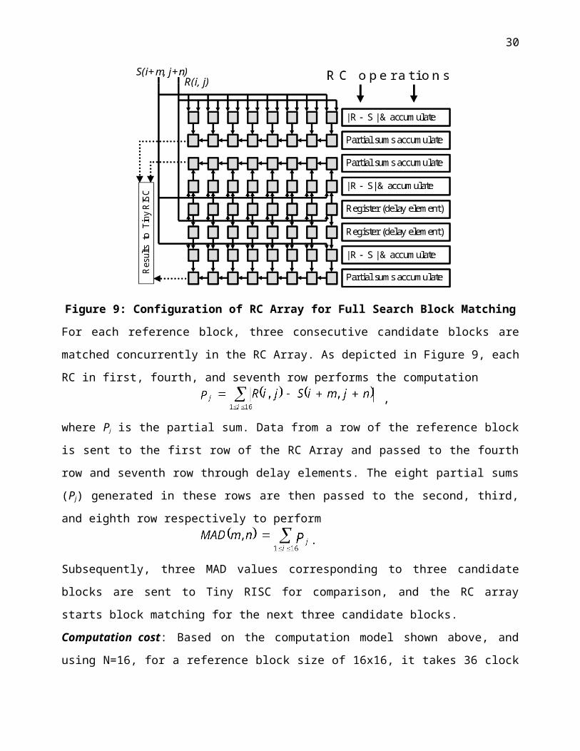
Figure 9 shows the configuration of RC Array for FSBM computation. Initially, one reference block
and the search area associated with it are loaded into one set of the frame buffer. The RC array
starts the matching process for the reference block resident in the frame buffer. During this
computation, another reference block and the search area associated with it are loaded into the other
set of the frame buffer. In this manner, data loading and computation time are overlapped.
Figure 9: Configuration of RC Array for Full Search Block Matching
For each reference block, three consecutive candidate blocks are matched concurrently in the RC
Array. As depicted in Figure 9, each RC in first, fourth, and seventh row performs the computation
,
where Pj is the partial sum. Data from a row of the reference block is sent to the first row of the RC
Array and passed to the fourth row and seventh row through delay elements. The eight partial sums
21

(Pj) generated in these rows are then passed to the second, third, and eighth row respectively to
perform
.
Subsequently, three MAD values corresponding to three candidate blocks are sent to Tiny RISC for
comparison, and the RC array starts block matching for the next three candidate blocks.
Computation cost: Based on the computation model shown above, and using N=16, for a reference
block size of 16x16, it takes 36 clock cycles to finish the matching of three candidate blocks. There
are (8+8+1)2 = 289 candidate blocks in each search area, and VHDL simulation results show that a
total of (102x[36+16])=5304 cycles are required to finish the matching of the whole search area.
The 16 extra cycles are for comparing the MAD results after each set of three block comparisons
and updating the motion vectors for the best match. If the image size is 352x288 pixels at 30 frames
per second (MPEG-2 main profile, low level), the number of reference blocks per frame is 22x18 =
396 (each reference block size is 16x16). Processing of an entire image frame would take
5304x396 = 2.1 x 10⁶ cycles.
Figure 10: MorphoSys M1 Performance for Motion Estimation -Giga Operations/S (GOPS)
At the anticipated clock rate of 100 MHz for MorphoSys, the computation time is 21.0 ms. This
is much smaller than frame period of 33.33ms. The context loading time is only 71 cycles, and since
a huge number of actual computation cycles are required before changing the configuration, its
22

effect is negligible. Figure 10 illustrates the performance of different generations of MorphoSys for
motion estimation in terms of giga-operations (109 operations) per second. We extrapolate the
performance results for future generations of M1, assuming future technologies will allow more
RCs on a single chip. These estimates are conservative and assume a fixed clock of 100 MHz
throughout. The GOPS figure for motion estimation is more than 60% of the peak value.
Performance Analysis: MorphoSys performance is compared with three ASIC architectures
implemented in [19], [20], [21] and Intel MMX instructions [22] for matching one 8x8 reference
block against its search area of 8 pixels displacement. The result is shown in Figure 11. The ASIC
architectures have same processing power (in terms of processing elements) as MorphoSys, though
they employ customized hardware units such as parallel adders to enhance performance. The
number of processing cycles for MorphoSys is comparable to the cycles required by the ASIC
designs. Pentium MMX takes almost 29000 cycles for the same task, which is almost thirty times
more than MorphoSys.
Figure 11: Performance Comparison for Motion Estimation
Since MorphoSys is not an ASIC, its performance with regard to these ASICs is significant. In a
subsequent sub-section, it shall be shown that this performance level enables the implementation of
an MPEG-2 encoder on MorphoSys.
23

1.1.1 Video Compression: Discrete Cosine Transform (DCT) for MPEG
The forward and inverse DCT are used in MPEG encoders and decoders. In the following analysis,
we consider an algorithm for fast 8-point 1-D DCT [23]. It involves 16 multiplications and 26
additions, leading to 256 multiplications and 416 additions for a 2-D implementation. The 1-D
algorithm is first applied to the rows (columns) of an input 8x8 image block, and then to the
columns (rows). The eight row (column) DCTs may be computed in parallel.
Mapping to RC Array: The standard block size for DCT in most image and video compression
standards is 8x8. Since the RC array has the same size, each pixel of the image block may be
directly mapped to each RC. Each pixel of the input block is stored in one RC.
Sequence of steps:
Loading input data: The 8x8 pixel block is loaded from the frame buffer to the RC Array. The data
bus between the frame buffer and the RC array allows concurrent loading of eight pixels at a time.
The entire block is loaded in eight cycles.
Row-column approach: Using the separability property, 1-D DCT along rows is computed. For row
(column) mode of operation, the configuration context is broadcast along columns (rows). Different
RCs within a row (column) of the array communicate using the three-layer interconnection network
to compute outputs for 1-D DCT. The coefficients needed for the computation are provided as
constants in context words. When 1-D DCT along rows (columns) is complete, the 1-D DCT along
columns (rows) are computed in a similar manner (Figure 12).
Each sequence of 1-D DCT [21] involves:
i. Butterfly computation: It takes three cycles to perform this using the inter-quad connectivity
layer of express lanes.
ii. Computation and re-arrangement: For 1-D DCT (row/column), the computation takes six
cycles. An extra cycle is used for re-arrangement of computed results.
24

Figure 12: Computation of 2-D DCT across rows/columns (without transposing)
Computation cost: The cost for computing 2-D DCT on an 8x8 block of the image is as follows: 6
cycles for butterfly, 12 cycles for both 1-D DCT computations and 3 cycles are used for re-
arrangement and scaling of data (giving a total of 21 cycles). This estimate is verified by VHDL
simulation. Assuming the data blocks to be present in the RC Array (through overlapping of data
load/store with computation cycles), it would take 0.49 ms for MorphoSys @ 100 MHz to compute
the DCT for all 8x8 blocks (396x6) in one frame of a 352x288 image. The cost of computing the 2-
D IDCT is the same, because the steps involved are similar. Context loading time is quite
significant at 270 cycles. However, this effect is minimized through transforming a large number of
blocks (typically 2376 blocks) before a different configuration is loaded.
Performance analysis: MorphoSys requires 21 cycles to complete 2-D DCT (or IDCT) on 8x8
block of pixel data. This is in contrast to 240 cycles required by Pentium MMX TM [22]. Even a
dedicated superscalar multi-media processor, [24] requires 201 clocks for the IDCT. REMARC [9]
takes 54 cycles to implement the IDCT, even though it uses 64 nano-processors. The DSP
multimedia video processor [18] computes the IDCT in 320 cycles. The relative performance
figures for MorphoSys and other implementations are given in Figure 13.
25
Figure 13: DCT/IDCT Performance Comparison (cycles)
Notably, MorphoSys performance scales linearly with the array size. For a 256 element RC array,
the number of operations possible per second would increase fourfold, with corresponding effect on
throughput for 2-D DCT and other algorithms. The performance figures (in GOPS) are summed up
in Figure 14 and these are more than 50% of the peak values. Once, again the figures are scaled for
future generations of MorphoSys M1, conservatively assuming a constant clock of 100 MHz.
Figure 14: Performance for DCT/IDCT -Giga Operations per Second (GOPS)
Some other points are worth noting: first, all rows (columns) perform the same computations, hence
they can be configured by a common context (thus enabling broadcast of context word), which
leads to saving in context memory space. Second, the RC array provides the option of broadcasting
26

context either across rows or across columns. This allows computation of second 1-D DCT without
transposing the data. Elimination of the transpose operation saves a considerable amount of cycles,
and is important for high performance. This operation generally consumes valuable cycle time. For
example, even hand-optimized version of IDCT code for Pentium MMX (that uses 64-bit registers)
needs at least 25 register-memory instructions for completing the transpose [22]. Processors, such as
the TMS320 series [18], also expend valuable cycle time on transposing data.
Precision analysis for IDCT: We conducted experiments for the precision of output IDCT for
MorphoSys as specified in the IEEE Standard [25]. Considering that MorphoSys is not a custom
design, and performs fixed-point operations, the results were impressive. We satisfied worst case
pixel error. The Overall Mean Square Error (OMSE) was within 15% of the reference value. The
majority of pixel locations also satisfied the worst case reference values for mean error and mean
square error.
Zigzag Scan: We also implemented the zig-zag scan function, even though MorphoSys is not
designed for applications that comprise of irregular accesses. But interestingly, we were able to use
selective context enabling feature of the RC Array to design a reasonable implementation. It is an
evidence of the flexibility of the MorphoSys model that we could map an application that is quite
diverse from the targeted applications for this architecture.
1.1.2 Mapping MPEG-2 Video Encoder to MorphoSys
We mapped all the functions for MPEG-2 video encoder, except the VLC encoding, to MorphoSys.
We assume that the Main profile, at the low level is being used. The maximum resolution required
for this level is 352x288 pixels per frame at 30 frames per second. We further assume that a group
of pictures consists of a sequence of four frames in the order IBBP (a typical choice for
broadcasting applications). The number of cycles required to compute each sub-task of the MPEG
encoder, for each macroblock type are listed in Table 2. Besides the actual computation cycles, we
also take into account the configuration load cycles and the cycles for loading the data from
memory.
27
Table 2: Performance Figures of MorphoSys M1 (64 RCs) for I, P and B Macro-blocks
Macroblock type /
MPEG functions
(in clock cycles)
Motion Estimation Motion Comp., DCT and Quant. ( / for
Inv Quant., IDCT, inv MC)
Context Mem Ld Compute Context Mem Ld Compute
I type macroblock 0 0 0 270/270 234/234 264/264
P type macroblock 71 334 5304 270/270 351/351 264/264
B type macroblock 71 597 10608 270 / 0 468 / 0 306/ 0
All the macro-blocks in each P and B frame are first subjected to motion estimation, then we
perform motion compensation, DCT and quantization for all macroblocks of a frame. These are
written out to frame storage in main memory. Finally, we perform inverse quantization, inverse
DCT and reverse motion prediction for each macroblock of I and P type frames. Each frame has
396 macroblocks, and the total number of cycles required for encoding each frame type are depicted
in Figure 15. It may be noted that motion estimation takes up almost 90% of the computation time
for P and B type frames.
Figure 15: MorphoSys performance for I, P and B frames (MPEG Video Encoder)
From the data in Figure 15, and using the assumption of frame sequence of IBBP, the total encoding
time is 117.3 ms. This is 88% of the total available time (133.3 ms). From empirical data values in
28

[24], the remaining 12% of available time is sufficient to compute VLC. We compare the MPEG
video encoder performance with that of REMARC [9] in Table 3. Even though MorphoSys figures
do not include VLC, they are almost two orders of magnitude less than REMARC. The Motion
Estimation algorithm (the major computation) is the same for REMARC and MorphoSys (FSBM).
Table 3: Comparison of MorphoSys MPEG Encoder with REMARC [9] MPEG Encoder
Frame Type / # of
cycles
Total clock cycles for
MorphoSys M1 (64 RCs)
Clock cycles for REMARC
[9] (64 nano-processors)
I frame 209,628 52.9 x 10⁶
P frame 2,378,987 69.6 x 10⁶
B frame 4,572,035 81.5 x 10⁶
1.1 Automatic Target Recognition (ATR)
Automatic Target Recognition (ATR) is the machine function of automatically detecting,
classifying, recognizing, and identifying an object. The ACS Surveillance challenge has been
quantified as the ability to search 40,000 square nautical miles per day with one meter resolution
[26]. The computation levels when targets are partially obscured reaches the hundreds-of-teraflops
range. There are many algorithmic choices available to implement an ATR system.
Figure 16: ATR Processing Model
29
The ATR processing model developed at Sandia National Laboratory is shown in Figure 16 ([27]
and [28]). This model was designed to detect partially obscured targets in Synthetic Aperture Radar
(SAR) images generated by the radar imager in real time. SAR Images (8-bits pixels) are input to a
focus-of-attention processor to identify the regions of interest (chips). These chips are thresholded
to generated binary images and the binary images are matched against binary target templates.
The first step is to generate the shapesum. The 128 x 128 x 8bits chip is bit sliced into eight
bitplanes. The system generates a shapesum by correlating each bitplane with the bright template
and then computing a weighted sum of the eight results. The chip is subsequently thresholded to
generate the binary image. Each pixel of the chip is compared with the shapesum and is set to a
binary data based on the following equation:
If Ai j shapesum > 0, Ai j 1
If Ai j shapesum < 0, Ai j 0, where Ai j represents the 8-bits pixels in chip
The most significant bit of the output register represents the result of the thresholding (in 2’s
complement representation). Each RC in the first column of the RC Array has a 8-bit packing
register. These registers collect the thresholding results of the RCs in each row. The data in the
packing registers is sent back to the frame buffer, and another set of 64 pixels of the chip are loaded
to RC array for thresholding.
Figure 17: Matching Process in Each RC
30

After the thresholding, a 128x128 binary image is generated and stored in the frame buffer. This
binary image is then matched against the target template using the bit correlator, shown in Figure
17. This template matching is similar to FSBM described in a previous sub-section. Each row of
8x8 target template is packed as an 8-bits number and loaded in RC array. All the candidate blocks
in the chip are correlated with target template. One column of RC array performs matching of one
target template and eight blocks are matched concurrently in the RC array.
In order to perform bit-level correlation, two bytes (16 bits) of image data are input to each RC. In
the first step, the 8 most significant bits of the image data are ANDed with the template data and a
special adder tree (implemented as custom hardware in each RC) is used to count the number of
one’s of the ANDed output to generate the correlation result. Then, the image data is shifted left
one bit and the process is repeated again to perform the matching of the second block. After the
image data is shifted eight times, a new 16-bits data is loaded and RC starts another correlation of
eight consecutive candidate blocks.
Performance analysis: For performance analysis, we choose the same system parameters that are
chosen for ATR systems implemented using Xilinx XC4010 FPGA [27] and Splash 2 system [28].
The image size of each chip is 128x128 pixels, and the template size is 8x8 bits. For 16 pairs of
target templates, the processing time is 21 ms for MorphoSys (at 100 MHz), 210 ms for the Xilinx
FPGA system [24], and 195 ms for the Splash 2 system [25]. Fig. 18 depicts relative performance.
Figure 18: Performance Comparison of MorphoSys for ATR
31

ATR System Specification: A quantified measure of the ATR problem states that 100 chips have to
be processed each second for a given target. The target has a pair of bright and surround templates
for each five degree rotation (72 pairs for full 360 degree rotation). Considering these requirements,
Table 4 compares the number of MorphoSys chips necessary to achieve this versus the number of
boards of the system described in [27] and [28]. Only nine chips of MorphoSys M1 (64 RCs)
would be needed to satisfy this specification, as compared to 90 boards for the system using FPGAs
[27] and 84 boards for the Splash system [28]. Once again, the figures for future generation
MorphoSys M1 chips assume a constant clock of 100 MHz
Table 4: ATR Performance Comparison (MorphoSys @ 100 MHz)
GOPS = Giga-
Operations/second
M1
(64 RCs)
M1
(128 RCs)
M1
(256 RCs)
Xilinx FPGA
[24]
Splash 2
[25]
ATR GOPS 14 28 56 1.4 1.52
No. of Chips/boards 9 chips 5 chips 3 chips 90 boards 84 boards
2. Conclusions and Future Work
In this paper, we presented a new model of reconfigurable architecture in the form of MorphoSys,
and mapped several applications to it. The results have validated this architectural model through
impressive performance for several of the target applications. We plan to implement MorphoSys on
an actual chip for practical evaluation.
Extensions for MorphoSys model: It may be noted that the MorphoSys architectural model is not
limited to using a basic/simple RISC processor for the main control processor. For the current
implementation, Tiny RISC is used only to validate the design model. However, several possible
extensions to this model are envisioned. One would be to use an advanced general-purpose
processor in conjunction with Tiny RISC (which would then function as an I/O processor for the
RC Array). Also, an advanced processor with multi-threading capability may be used as the main
processor. This would enable concurrent processing of the RC Array and the main processor.
32

Another potential focus is the RC Array. For this implementation, the array has been fine-tuned for
data-parallel, computation intensive tasks. However, the design model allows other versions, too.
For e.g., a suitably designed RC Array may be used for a different application class, such as stream
processing, high-precision signal processing, bit-level operations, control-intensive applications,
etc.
Based on the above, we visualize that MorphoSys may be the precursor of a generation of general-
purpose processors that have a specialized reconfigurable component, designed for multimedia or
some other significant class of applications.
3. Acknowledgments
This research is supported by Defense and Advanced Research Projects Agency (DARPA) of the
Department of Defense under contract number F-33615-97-C-1126. We express thanks to Prof.
Eliseu M.C. Filho, Prof. Tomas Lang, and Prof. Walid Najjar for their useful and incisive
comments, Robert Heaton (Obsidian Technology) for his contributions towards the physical design
of MorphoSys and Ms. Kerry Hill of Air Force Research Laboratory, for her constructive feedback.
We acknowledge the contributions of Maneesha Bhate, Matthew Campbell, Benjamin U-Tee
Cheah, Alexander Gascoigne, Nambao Van Le, Rafael Maestre, Robert Powell, Rei Shu, Lingling
Sun, Cesar Talledo, Eric Tan, Timothy Truong, and Tom Truong; all of whom have been associated
with the development of MorphoSys models and application mapping.
References:
1. W. H. Mangione-Smith, B Hutchings, D. Andrews, A. DeHon, C. Ebeling, R. Hartenstein, O.
Mencer, J. Morris, K. Palem, V. K. Prasanna, H. A. E. Spaaneburg, “Seeking Solutions in
Configurable Computing,” IEEE Computer, Dec 1997, pp. 38-43
2. S. Brown and J. Rose, “Architecture of FPGAs and CPLDs: A Tutorial,” IEEE Design and Test
of Computers, Vol. 13, No. 2, pp. 42-57, 1996
3. D. Chen , J. Rabaey, “Reconfigurable Multi-processor IC for Rapid Prototyping of Algorithmic-
Specific High-Speed Datapaths,” IEEE Journal of Solid-State Circuits, V. 27, No. 12, Dec 92
33

4. R. Hartenstein and R. Kress, “A Datapath Synthesis System for the Reconfigurable Datapath
Architecture,” Proc. of Asia and South Pacific Design Automation Conf., 1995, pp. 479-484
5. E. Tau, D. Chen, I. Eslick, J. Brown and A. DeHon, “A First Generation DPGA
Implementation,” FPD’95, Canadian Workshop of Field-Programmable Devices, May 1995
6. E. Mirsky and A. DeHon, “MATRIX: A Reconfigurable Computing Architecture with
Configurable Instruction Distribution and Deployable Resources,” Proceedings of IEEE
Symposium on FPGAs for Custom Computing Machines, 1996, pp.157-66
7. J. R. Hauser and J. Wawrzynek, “Garp: A MIPS Processor with a Reconfigurable Co-
processor,” Proc. of the IEEE Symposium on FPGAs for Custom Computing Machines, 1997
8. C. Ebeling, D. Cronquist, and P. Franklin, “Configurable Computing: The Catalyst for High-
Performance Architectures,” Proceedings of IEEE International Conference on Application-
specific Systems, Architectures and Processors, July 1997, pp. 364-72
9. T. Miyamori and K. Olukotun, “A Quantitative Analysis of Reconfigurable Coprocessors for
Multimedia Applications,” Proceedings of IEEE Symposium on Field-Programmable Custom
Computing Machines, April 1998
10. J. Babb, M. Frank, V. Lee, E. Waingold, R. Barua, M. Taylor, J. Kim, S. Devabhaktuni, A.
Agrawal, “The RAW Benchmark Suite: computation structures for general-purpose computing,”
Proc. IEEE Symposium on Field-Programmable Custom Computing Machines, FCCM 97,
1997, pp. 134-43
11. M. Gokhale, W. Holmes, A. Kopser, S. Lucas, R. Minnich, D. Sweely, D. Lopresti, “Building
and Using a Highly Parallel Programmable Logic Array,” IEEE Computer, pp. 81-89, Jan. 1991
12. P. Bertin, D. Roncin, and J. Vuillemin, “Introduction to Programmable Active Memories,” in
Systolic Array Processors, Prentice Hall, 1989, pp. 300-309
13. Xilinx, the Programmable Logic Data Book, 1994
14. A. Abnous, C. Christensen, J. Gray, J. Lenell, A. Naylor and N. Bagherzadeh, “ Design and
Implementation of the Tiny RISC microprocessor,” Microprocessors and Microsystems, Vol.
16, No. 4, pp. 187-94, 1992
34

15. Practical Programming in Tcl and Tk, 2nd edition, by Brent B. Welch, Prentice-Hall, 1997
16. SUIF Compiler system, The Stanford SUIF Compiler Group, http://suif.stanford.edu
17. ISO/IEC JTC1 CD 13818. Generic coding of moving pictures, 1994 (MPEG-2 standard)
18. F. Bonomini, F. De Marco-Zompit, G. A. Mian, A. Odorico, D. Palumbo, “Implementing an
MPEG2 Video Decoder Based on TMS320C80 MVP,” SPRA 332, Texas Instr., Sep 1996
19. C. Hsieh, T. Lin, “VLSI Architecture For Block-Matching Motion Estimation Algorithm,” IEEE
Trans. on Circuits and Systems for Video Tech., vol. 2, pp. 169-175, June 1992
20. S.H Nam, J.S. Baek, T.Y. Lee and M. K. Lee, “ A VLSI Design for Full Search Block Matching
Motion Estimation,” Proc. of IEEE ASIC Conference, Rochester, NY, Sep 1994, pp. 254-7
21. K-M Yang, M-T Sun and L. Wu, “ A Family of VLSI Designs for Motion Compensation Block
Matching Algorithm,” IEEE Trans. on Circuits and Systems, V. 36, No. 10, Oct 89, pp. 1317-25
22. Intel Application Notes for Pentium MMX, http://developer.intel.com/drg/mmx/appnotes/
23. W-H Chen, C. H. Smith and S. C. Fralick, “A Fast Computational Algorithm for the Discrete
Cosine Transform,” IEEE Trans. on Comm., vol. COM-25, No. 9, September 1977
24. T. Arai, I. Kuroda, K. Nadehara and K. Suzuki, “V830R/AV: Embedded Multimedia
Superscalar RISC Processor,” IEEE MICRO, Mar/Apr 1998, pp. 36-47
25. “IEEE Standard Specifications for the Implementation of 8x8 Inverse Discrete Cosine
Transform,” Std. 1180-1990, IEEE, Dec. 1990
26. Challenges for Adaptive Computing Systems, Defense and Advanced Research Projects Agency
(DARPA), www.darpa.mil/ito/research/acs/challenges.html
27. J. Villasenor, B. Schoner, K. Chia, C. Zapata, H. J. Kim, C. Jones, S. Lansing, and B.
Mangione-Smith, “ Configurable Computing Solutions for Automatic Target Recognition,”
Proceedings of IEEE Workshop on FPGAs for Custom Computing Machines, April 1996
28. M. Rencher and B.L. Hutchings, " Automated Target Recognition on SPLASH 2," Proceedings
of IEEE Symposium on FPGAs for Custom Computing Machines, April 1997
35