
More SPICE Examples - diyhpl
46
© January 1, 2014 Dr. Lynn Fuller More SPICE Examples Page 1 Rochester Institute of Technology Microelectronic Engineering ROCHESTER INSTITUTE OF TECHNOLOGY MICROELECTRONIC ENGINEERING More SPICE Examples Dr. Lynn Fuller Electrical and Microelectronic Engineering Rochester Institute of Technology 82 Lomb Memorial Drive Rochester, NY 14623-5604 Tel (585) 475-2035 Fax (585) 475-5041 Dr. Fuller’s Webpage: http://people.rit.edu/lffeee Email: [email protected] Dept Webpage: http://www.microe.rit.edu 1-1-2014 SPICE_More_Examples.ppt
Transcript of More SPICE Examples - diyhpl
© January 1, 2014 Dr. Lynn Fuller
More SPICE Examples
Page 1
Rochester Institute of Technology
Microelectronic Engineering
ROCHESTER INSTITUTE OF TECHNOLOGY
MICROELECTRONIC ENGINEERING
More SPICE Examples
Dr. Lynn Fuller Electrical and Microelectronic Engineering
Rochester Institute of Technology 82 Lomb Memorial Drive Rochester, NY 14623-5604
Tel (585) 475-2035 Fax (585) 475-5041
Dr. Fuller’s Webpage: http://people.rit.edu/lffeee Email: [email protected]
Dept Webpage: http://www.microe.rit.edu
1-1-2014 SPICE_More_Examples.ppt

© January 1, 2014 Dr. Lynn Fuller
More SPICE Examples
Page 2
Rochester Institute of Technology
Microelectronic Engineering
ADOBE PRESENTER
This PowerPoint module has been published using Adobe Presenter. Please click
on the Notes tab in the left panel to read the instructors comments for each slide.
Manually advance the slide by clicking on the play arrow or pressing the page
down key.
© January 1, 2014 Dr. Lynn Fuller
More SPICE Examples
Page 3
Rochester Institute of Technology
Microelectronic Engineering
OUTLINE
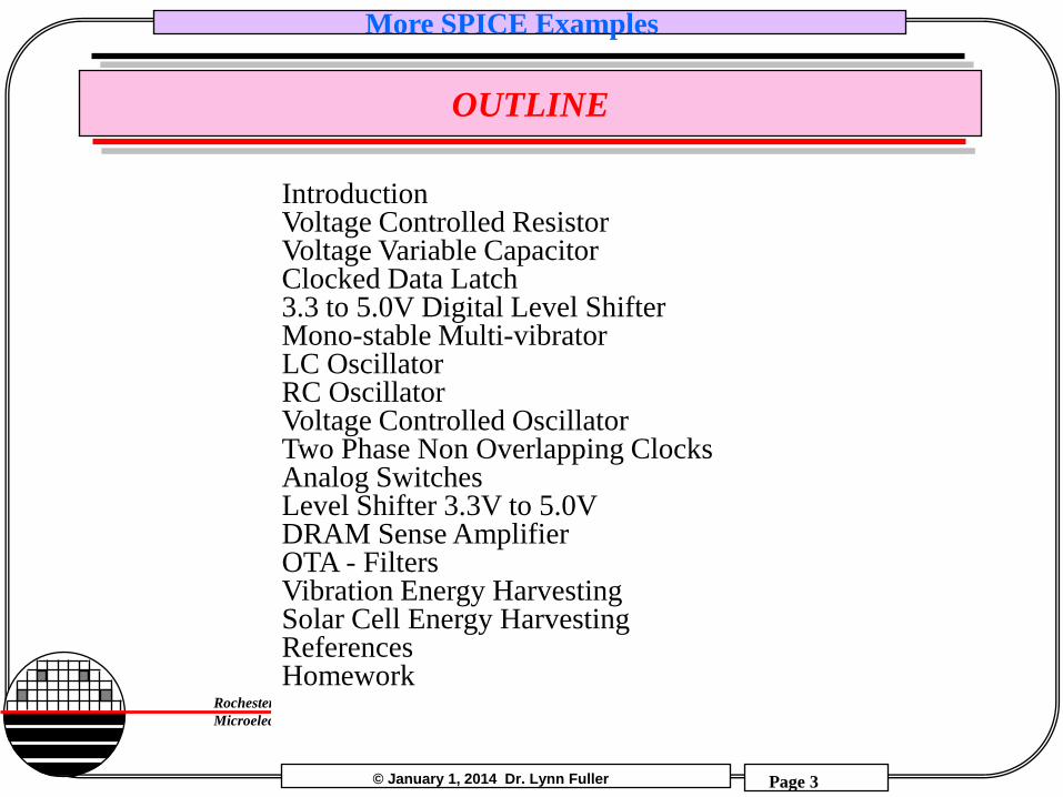
Introduction Voltage Controlled Resistor Voltage Variable Capacitor Clocked Data Latch 3.3 to 5.0V Digital Level Shifter Mono-stable Multi-vibrator LC Oscillator RC Oscillator Voltage Controlled Oscillator Two Phase Non Overlapping Clocks Analog Switches Level Shifter 3.3V to 5.0V DRAM Sense Amplifier OTA - Filters Vibration Energy Harvesting Solar Cell Energy Harvesting References Homework
© January 1, 2014 Dr. Lynn Fuller
More SPICE Examples
Page 4
Rochester Institute of Technology
Microelectronic Engineering
INTRODUCTION
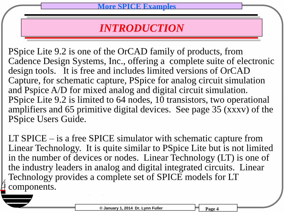
PSpice Lite 9.2 is one of the OrCAD family of products, from Cadence Design Systems, Inc., offering a complete suite of electronic design tools. It is free and includes limited versions of OrCAD Capture, for schematic capture, PSpice for analog circuit simulation and Pspice A/D for mixed analog and digital circuit simulation. PSpice Lite 9.2 is limited to 64 nodes, 10 transistors, two operational amplifiers and 65 primitive digital devices. See page 35 (xxxv) of the PSpice Users Guide. LT SPICE – is a free SPICE simulator with schematic capture from Linear Technology. It is quite similar to PSpice Lite but is not limited in the number of devices or nodes. Linear Technology (LT) is one of the industry leaders in analog and digital integrated circuits. Linear Technology provides a complete set of SPICE models for LT components.

© January 1, 2014 Dr. Lynn Fuller
More SPICE Examples
Page 5
Rochester Institute of Technology
Microelectronic Engineering
VOLTAGE CONTROLLED RESISTOR
Voltage Controlled Resistor inside dashed box
V1 is to test I-V Characteristics

© January 1, 2014 Dr. Lynn Fuller
More SPICE Examples
Page 6
Rochester Institute of Technology
Microelectronic Engineering
VOLTAGE CONTROLLED RESISTOR
The green line is for control voltage=1.0 giving R=2Kohms, the blue is for control voltage=1.5 giving R=3Kohms. Imax=2Volts/2Kohms= 1.0mA Or Imax=2Volts/3Kohms= 0.66mA
Vcontrol=1.0
Vcontrol=1.5

© January 1, 2014 Dr. Lynn Fuller
More SPICE Examples
Page 7
Rochester Institute of Technology
Microelectronic Engineering
VOLTAGE VARIABLE CAPACITOR
http://www.beigebag.com/case_var_cap.htm

© January 1, 2014 Dr. Lynn Fuller
More SPICE Examples
Page 8
Rochester Institute of Technology
Microelectronic Engineering
CLOCKED DATA LATCH WITH AND-OR-INVERT GATE
VDD = 1.8 V
CLK
D
Q
CLK _ Q _
D
VDD
10 nF
CLK
D
Q
_ Q
CMOS And Or Invert Gate

© January 1, 2014 Dr. Lynn Fuller
More SPICE Examples
Page 9
Rochester Institute of Technology
Microelectronic Engineering
CLOCKED DATA LATCH WITH AND-OR-INVERT GATE
CMOS Clocked Data Latch using AND-OR-INV Gates
Inverter
AND-OR-INV AND-OR-INV

© January 1, 2014 Dr. Lynn Fuller
More SPICE Examples
Page 10
Rochester Institute of Technology
Microelectronic Engineering
3.3V to 5.0 V DIGITAL LEVEL SHIFTER
Converts 0-3.3 V digital signals to 0-5.0 volt signals (An inverter following the output may be used)
3.3v Signal
5v Signal

© January 1, 2014 Dr. Lynn Fuller
More SPICE Examples
Page 11
Rochester Institute of Technology
Microelectronic Engineering
MONOSTABLE MULTIVIBRATOR
VDD
C R
VDD = 5 V
Vout
V2 V3 VC 1 2 3
t
1 s
0
Vtrigger
27 kΩ
0.01 F
A short pulse will cause Vout to go high and stay high for a time determined by R and C

© January 1, 2014 Dr. Lynn Fuller
More SPICE Examples
Page 12
Rochester Institute of Technology
Microelectronic Engineering
LC OSCILLATOR
f = 1/(2 pi (sq root LC)) = 225 KHz
Two cycles in 0.009 ms gives 222KHz

© January 1, 2014 Dr. Lynn Fuller
More SPICE Examples
Page 13
Rochester Institute of Technology
Microelectronic Engineering
NMOS INVERTER WITH HYSTERESIS
M4 is used to change the threshold voltage of M3 by body effect through changing the voltage source-to-substrate of M3depending on if Vout is high or low. Transition voltage depends on direction of sweep.
Inverter on Left
Inverter on Right
V(In) From low-to-high
V(In2) From high-to-low

© January 1, 2014 Dr. Lynn Fuller
More SPICE Examples
Page 14
Rochester Institute of Technology
Microelectronic Engineering
CMOS INVERTER WITH HYSTERESIS
Replace the pull up resistor with PMOSFETs

© January 1, 2014 Dr. Lynn Fuller
More SPICE Examples
Page 15
Rochester Institute of Technology
Microelectronic Engineering
DIMENSIONS OF THE TRANSISTORS
NMOS PMOS
L 2u 2u
W 40u 40u
AD 17ux40u=680p 17ux40u=680p
AS 17ux40u=680p 17ux40u=680p
PD 2x(17u+40u)=114u 2x(17u+40u)=114u
PS 2x(17u+40u)=114u 2x(17u+40u)=114u
Right mouse click on each transistor and add these values to the properties/attributes.
Dimensions of transistors in Gate Array
W = 40 µm Ldrawn = 2.5µm Lpoly = 2.0µm Leff = 1.5 µm\ Pd=680p Ad=114u

© January 1, 2014 Dr. Lynn Fuller
More SPICE Examples
Page 16
Rochester Institute of Technology
Microelectronic Engineering
CMOS RC OSCILLATOR USING INVERTER W HYSTERESIS
C1=10p gives f=10MHz
C1=100p gives f= 1 MHz

© January 1, 2014 Dr. Lynn Fuller
More SPICE Examples
Page 17
Rochester Institute of Technology
Microelectronic Engineering
CMOS OSCILLATOR REPLACE R WITH MOSFETS
C1 = 100pF gives f=4MHz
C1 = 10pF gives f=16MHz

© January 1, 2014 Dr. Lynn Fuller
More SPICE Examples
Page 18
Rochester Institute of Technology
Microelectronic Engineering
VOLTAGE CONTROLLED OSCILLATOR

© January 1, 2014 Dr. Lynn Fuller
More SPICE Examples
Page 19
Rochester Institute of Technology
Microelectronic Engineering
ANALOG SWITCHES
For current flowing to the right (ie V1>V2) the PMOS transistor will be on if V1 is greater than the threshold voltage, the NMOS transistor will be on if V2 is <4 volts. If we are charging up a capacitor load at node 2 to 5 volts, initially current will flow through NMOS and PMOS but once V2 gets above 4 volts the NMOS will be off. If we are trying to charge up V2 to V1 = +1 volt the PMOS will never be on. A complementary situation occurs for current flow to the left. Single transistor switches can be used if we are sure the Vgs will be more than the threshold voltage for the specific circuit application. (or use larger voltages on the gates)
NMOS Vt=+1
PMOS Vt= -1
D S
I
zero
V1 V2
+5
S D

© January 1, 2014 Dr. Lynn Fuller
More SPICE Examples
Page 20
Rochester Institute of Technology
Microelectronic Engineering
ANALOG SWITCH
Switch Off Switch On
Analog Input V3 is a sine wave with 2.5v offset and amplitude of 2.5v
When V2 is low the switch is on

© January 1, 2014 Dr. Lynn Fuller
More SPICE Examples
Page 21
Rochester Institute of Technology
Microelectronic Engineering
ANALOG SWITCH FOR DUAL SUPPLY
This example is for a mixed digital and analog circuit. For example a 3.3 volt digital logic and +/- 5 volt analog op amp. The signal going thru the switch is +/-5 volts.
This circuit works if V3 is always positive but does not work in this example because Vin goes negative

© January 1, 2014 Dr. Lynn Fuller
More SPICE Examples
Page 22
Rochester Institute of Technology
Microelectronic Engineering
ANALOG SWITCH FOR DUAL SUPPLY
This example is for a mixed digital and analog circuit. For example a 3.3 volt digital logic and +/- 12 volt analog op amp.
D S
0-5V Logic Control
Vout
+5
S D Vin
+V
-V
© January 1, 2014 Dr. Lynn Fuller
More SPICE Examples
Page 23
Rochester Institute of Technology
Microelectronic Engineering
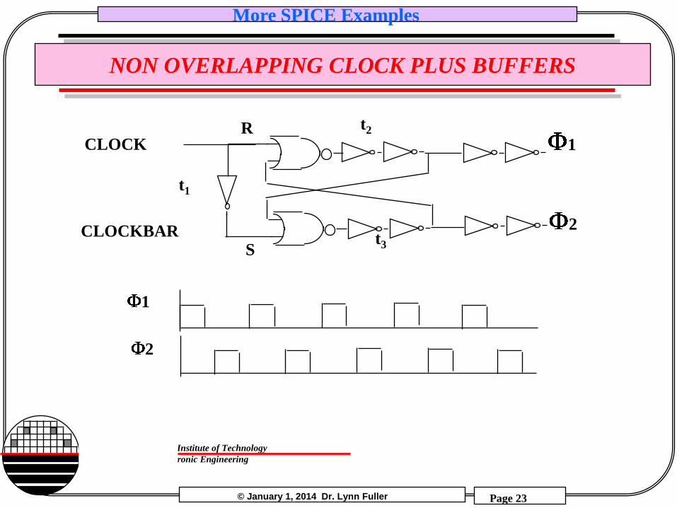
NON OVERLAPPING CLOCK PLUS BUFFERS
CLOCKBAR
CLOCK 1
2 t3
t2
t1
S
R
1
2

© January 1, 2014 Dr. Lynn Fuller
More SPICE Examples
Page 24
Rochester Institute of Technology
Microelectronic Engineering
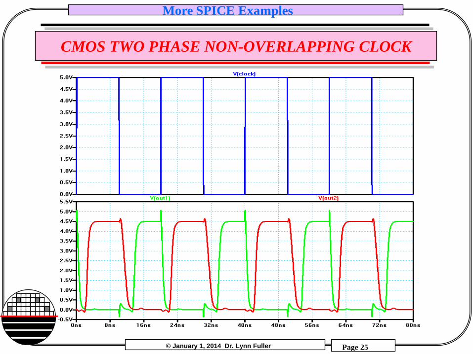
CMOS TWO PHASE NON-OVERLAPPING CLOCK
© January 1, 2014 Dr. Lynn Fuller
More SPICE Examples
Page 25
Rochester Institute of Technology
Microelectronic Engineering
CMOS TWO PHASE NON-OVERLAPPING CLOCK

© January 1, 2014 Dr. Lynn Fuller
More SPICE Examples
Page 26
Rochester Institute of Technology
Microelectronic Engineering
DRAM SENSE AMPLIFER DETAILS
Digit Line Reference Digit Line
C0
Vdd/2
Vdd
Vdd/2
s
s
p
Q9 Q8
Q5
Q6
Q2 Q1
Q3 Q4
Q7 is turned on with signal p precharging the two digit lines to Vdd/2
Q7
Note: the memory is organized into two arrays so that one can be used as the reference for the other. (with basically identical digit line capacitance) WL0
Vdd/2
D0
D0*

© January 1, 2014 Dr. Lynn Fuller
More SPICE Examples
Page 27
Rochester Institute of Technology
Microelectronic Engineering
SENSE AMPLIFIER DETAILS
s goes high and the data in the selected memory cell is sensed. The word line WL0 goes high and the charge on selected capacitor C0 is shared with the capacitance of the digit line D0. If a “1” was stored in C0 the voltage on D0 will initially be a little higher than Vdd/2. The voltage on the reference digit line will initially be Vdd/2. The crosscoupled inverters amplify these starting voltage and bring the digit line D0 to Vdd and D0* to zero volts. The capacitor C0 is recharged (refreshed) at the same time it is read. If a “0” was stored in C0 the voltage on D0 will initially be a little lower than Vdd/2. The crosscoupled inverters bring D0 to zero volts, refreshing C0 and providing a one for an output on D0*.

© January 1, 2014 Dr. Lynn Fuller
More SPICE Examples
Page 28
Rochester Institute of Technology
Microelectronic Engineering
SENSE AMPLIFER WAVEFORMS
D0
D0*
s
s

© January 1, 2014 Dr. Lynn Fuller
More SPICE Examples
Page 29
Rochester Institute of Technology
Microelectronic Engineering
OPERATIONAL TRANSCONDUCTANCE AMPLIFIER
+V
-V
Vin+ Vin-
M1 M2
M3
M5
M4
CMOS Realization
5
1
2
4
Va +
V- Ibias
V+
Vb Iout
-
Va +
Vb
Iout
- Ibias
Iout
gm(Va-Vb) Vref
M3 M4
Note: gm is set by Ibias
© January 1, 2014 Dr. Lynn Fuller
More SPICE Examples
Page 30
Rochester Institute of Technology
Microelectronic Engineering
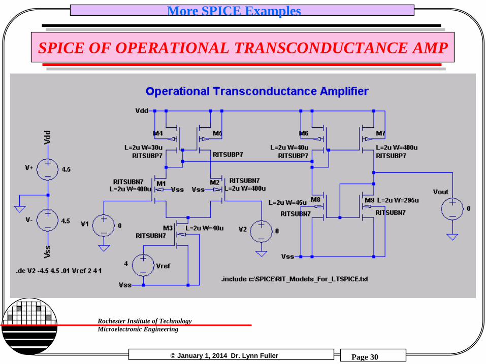
SPICE OF OPERATIONAL TRANSCONDUCTANCE AMP

© January 1, 2014 Dr. Lynn Fuller
More SPICE Examples
Page 31
Rochester Institute of Technology
Microelectronic Engineering
TRANSCONDUCTANCE FOR Vref=2,3,4 volts
Iout versus Vin Gm = slope of Iout vs Vin
Gm and Ibias

© January 1, 2014 Dr. Lynn Fuller
More SPICE Examples
Page 32
Rochester Institute of Technology
Microelectronic Engineering
BIQUAD FILTER
VC
+
V- Ibias1
V+
-
+
V- Ibias3
V+
Vout -
VA +
V- Ibias5
V+
-
+
V- Ibias2
V+
-
C2
C1
VB +
V- Ibias4
V+
-
gm1
gm4
gm3 gm2
gm5

© January 1, 2014 Dr. Lynn Fuller
More SPICE Examples
Page 33
Rochester Institute of Technology
Microelectronic Engineering
BIQUAD FILTER
Vout = (s2C1C2Vc + s C1 gm4 Vb + gm2 gm5 Va)/(s2C1C2+ sC1gm3+gm2gm1)
This filter can be used as a low-pass, high-pass, bandpass, bandrejection and all pass filter. Depending on the C and gm values a Butterworth, Chebyshev, Elliptic or any other configuration can be achieved For example: let Vc=Vb=0 and Va=Vin, also let all gm be equal, then Vout = Vin / (s2C1C2/ gmgm + sC1/gm + 1) which is a second order low pass filter with corner frequency at c = gm / C1C2 and Q = C2/C1

© January 1, 2014 Dr. Lynn Fuller
More SPICE Examples
Page 34
Rochester Institute of Technology
Microelectronic Engineering
COMPARISON OF DIFFERENT FILTER DESIGNS
Elliptic
Butterworth
Chebychev
gain
frequency
Lowpass Filters
Elliptic is flat in the band pass region, has the steepest transition to band stop region but has some gain in the band stop region
Butterworth is flat in the band pass region, has the least steep transition to band stop region
Chebychev is not flat in the band pass region, has a steeper transition to band stop region than Butterworth
© January 1, 2014 Dr. Lynn Fuller
More SPICE Examples
Page 35
Rochester Institute of Technology
Microelectronic Engineering
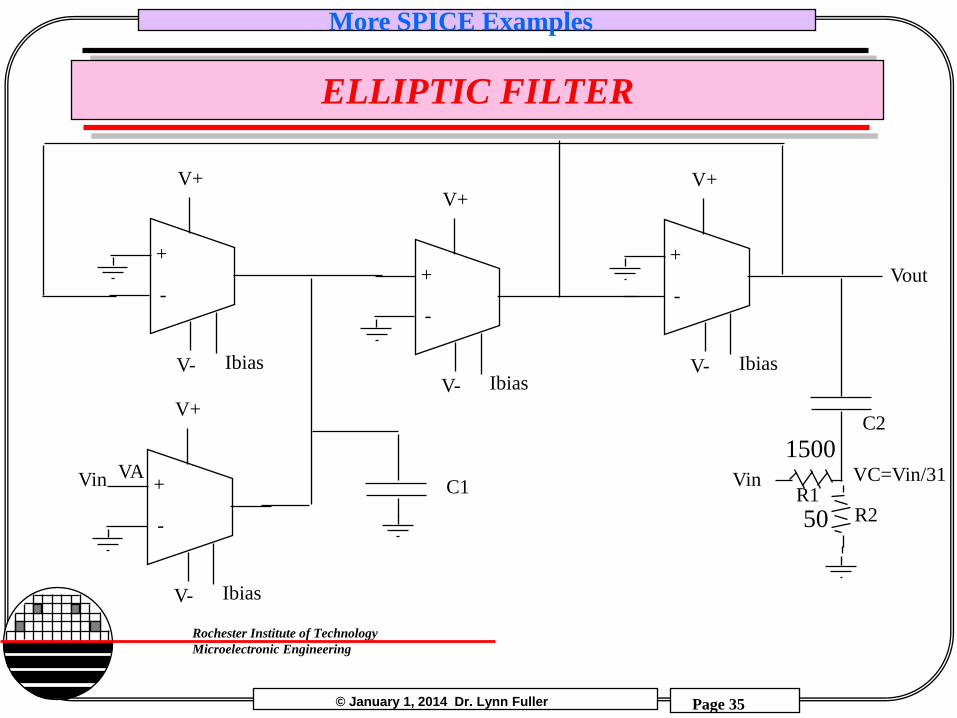
ELLIPTIC FILTER
VC=Vin/31
+
V- Ibias
V+
-
+
V- Ibias
V+
Vout -
Vin +
V- Ibias
V+
-
+
V- Ibias
V+
-
C2
C1
R2 R1
1500
50
Vin VA

© January 1, 2014 Dr. Lynn Fuller
More SPICE Examples
Page 36
Rochester Institute of Technology
Microelectronic Engineering
VIBRATION ENERGY HARVESTER
5V / 0.035F

© January 1, 2014 Dr. Lynn Fuller
More SPICE Examples
Page 37
Rochester Institute of Technology
Microelectronic Engineering
VOLTAGE MULTIPLIER

© January 1, 2014 Dr. Lynn Fuller
More SPICE Examples
Page 38
Rochester Institute of Technology
Microelectronic Engineering
IXOLAR SOLAR CELL – MEASURED CHARACTERISTICS
IXOLAR – KXOB22-12X1
MEASURED ISC Cell 1 Cell2 Measured Light Intensity Room Light at Desk Top 0.0705mA 0.0509mA 300 Lux Close to Light Fixture 1.574mA 1.560mA XXX Lux Highest Microscope Illuminator Setting 51.2mA 48.6mA XXX Lux Overhead Projector 13.6mA 15mA XX Lux (~2.5mW/cm2) Direct Sunlight Through Window 16.0mA 16.0mA 65,000 Lux Dark Current 58.1nA 17.8nA zero Series Resistance 1.6966Ω 1.5363Ω Parallel Resistance >1MEG >1MEG
(~25w/m2 = ~2.5mW/cm2)
© January 1, 2014 Dr. Lynn Fuller
More SPICE Examples
Page 39
Rochester Institute of Technology
Microelectronic Engineering
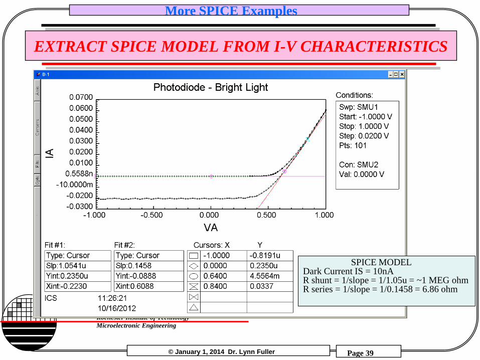
EXTRACT SPICE MODEL FROM I-V CHARACTERISTICS
SPICE MODEL Dark Current IS = 10nA R shunt = 1/slope = 1/1.05u = ~1 MEG ohm R series = 1/slope = 1/0.1458 = 6.86 ohm

© January 1, 2014 Dr. Lynn Fuller
More SPICE Examples
Page 40
Rochester Institute of Technology
Microelectronic Engineering
LTSPICE SIMULATION OF 7MMX22MM SOLAR CELL

© January 1, 2014 Dr. Lynn Fuller
More SPICE Examples
Page 41
Rochester Institute of Technology
Microelectronic Engineering
BLOCK DIAGRAM FOR LTC3105
© January 1, 2014 Dr. Lynn Fuller
More SPICE Examples
Page 42
Rochester Institute of Technology
Microelectronic Engineering
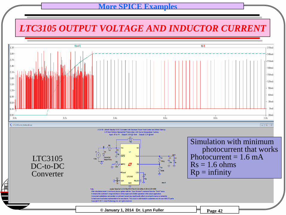
LTC3105 OUTPUT VOLTAGE AND INDUCTOR CURRENT
Simulation with minimum photocurrent that works Photocurrent = 1.6 mA Rs = 1.6 ohms Rp = infinity
LTC3105 DC-to-DC Converter

© January 1, 2014 Dr. Lynn Fuller
More SPICE Examples
Page 43
Rochester Institute of Technology
Microelectronic Engineering
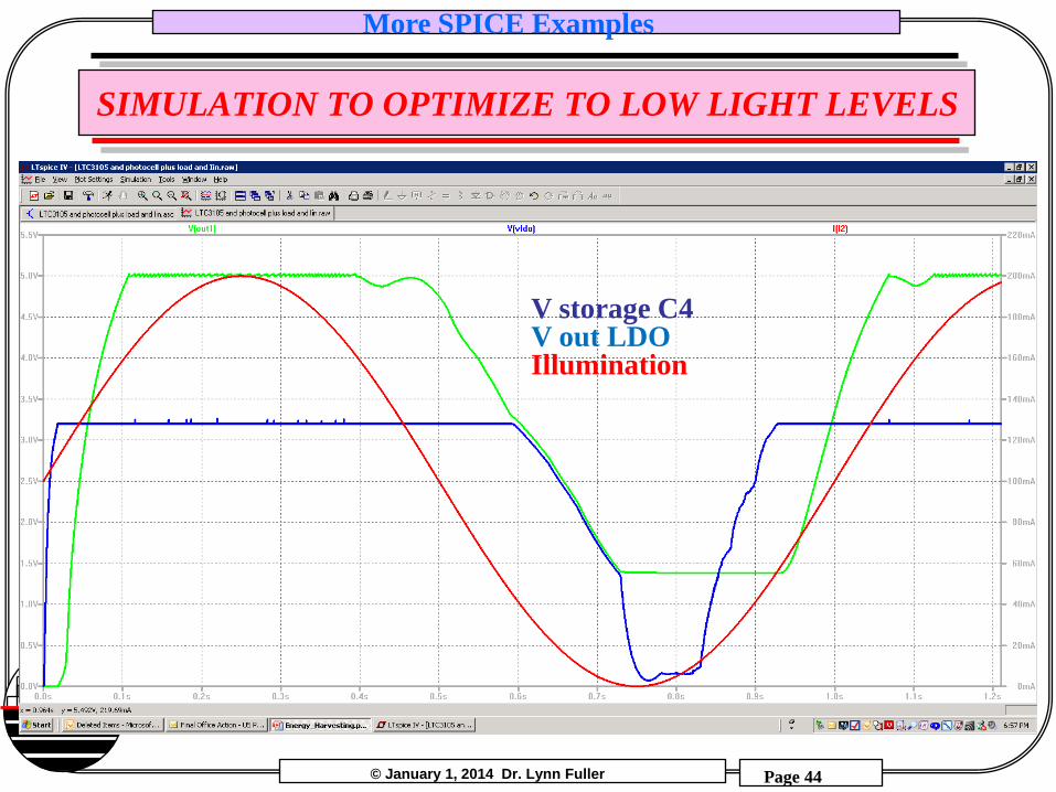
SIMULATION TO OPTIMIZE TO LOW LIGHT LEVELS
© January 1, 2014 Dr. Lynn Fuller
More SPICE Examples
Page 44
Rochester Institute of Technology
Microelectronic Engineering
SIMULATION TO OPTIMIZE TO LOW LIGHT LEVELS
V storage C4 V out LDO Illumination

© January 1, 2014 Dr. Lynn Fuller
More SPICE Examples
Page 45
Rochester Institute of Technology
Microelectronic Engineering
REFERENCES
1. MOSFET Modeling with SPICE, Daniel Foty, 1997, Prentice Hall, ISBN-0-13-227935-5 2. Operation and Modeling of the MOS Transistor, 2nd Edition, Yannis Tsividis,
1999, McGraw-Hill, ISBN-0-07-065523-5 3. UTMOST III Modeling Manual-Vol.1. Ch. 5. From Silvaco International. 4. ATHENA USERS Manual, From Silvaco International. 5. ATLAS USERS Manual, From Silvaco International. 6. Device Electronics for Integrated Circuits, Richard Muller and Theodore
Kamins, with Mansun Chan, 3rd Edition, John Wiley, 2003, ISBN 0-471-59398-2 7. ICCAP Manual, Hewlet Packard 8. PSpice Users Guide.

© January 1, 2014 Dr. Lynn Fuller
More SPICE Examples
Page 46
Rochester Institute of Technology
Microelectronic Engineering
HOMEWORK – MORE SPICE EXAMPLES
Do SPICE for one of the following: 1. Use SPICE to investigate an elliptic filter. 2. Do a SPICE simulation for an Analog Switch that can pass positive
and negative voltages. (+/-12 volts using 0- 5 volt logic) 3. Do a SPICE simulation for the two phase non-overlapping clock
circuit.


![75 [More] Content Marketing Examples](https://static.fdocuments.us/doc/165x107/58d108c41a28ab823e8b5513/75-more-content-marketing-examples.jpg)
