Moores Law into the 1x era - American Vacuum Society · Moore’s Law Continues into the 1x-nm Era...
35
Moore’s Law Continues into the 1x-nm Era NCCAVS JTG User Group Meeting SemiconWest July 14, 2016 Dick James Senior Fellow/Technology Analyst Chipworks
-
Upload
hoangquynh -
Category
Documents
-
view
216 -
download
0
Transcript of Moores Law into the 1x era - American Vacuum Society · Moore’s Law Continues into the 1x-nm Era...

Moore’s Law Continues into the 1x-nm Era
NCCAVS JTG User Group Meeting SemiconWest July 14, 2016
Dick James
Senior Fellow/Technology Analyst
Chipworks

The Last Few Generations
2
And the changes we’ve seen..
Litho 248 nm 193 nm dry 193 nm wet DP
Low-k dielectrics 1st gen 2nd gen 3rd gen
Strained channels
High-k, metal-gate
FinFET
14nm
All content © 2016, Chipworks Inc. All rights reserved.

3
�Planar transistor high-k, metal-gate (HKMG) parts are in volume production down to the 20-nm generation, in gate-first and gate-last technologies
�HKMG tri-gate (finFET) devices are now also manufactured in high volume, in CPU and SoCformats
�Let’s look at some!
Introduction
All content © 2016, Chipworks Inc. All rights reserved.

Qualcomm MDM9235 (TSMC 20 nm HPM HKMG Process)
4 All content © 2016, Chipworks Inc. All rights reserved.

5
20HPM PMOS Transistors
All content © 2016, Chipworks Inc. All rights reserved.
� Second-generation HKMG process
– hi-k formed after polySi removal
(like Intel 32-nm)
� PMOS gate stack formed before
NMOS
� Contacted gate pitch (CGP) ~90
nm
� Minimum observed gate length
(MOLg) ~28 nm,
� Tox ~1.4 nm, thi-k ~1.3 nm – cf 28HP tox
1.4 nm, 28 HPM 1.5 nm, 28HPL 2.0
nm
� Work-function materials similar to
28-nm process – PMOS is TiN
� Raised source/drain epi with e-
SiGe, graded -> ~40% Ge
SiOHfO
PMOS WF TiNTaN
TiN
TiAlON
TiAlN
P/NMOS gate transition
PMOS NMOS

6
20HPM NMOS Transistors
� Minimum observed gate length 31 nm
� Raised source/drains, stacking faults for stress (like Intel 32-nm)
� TiAlN work-function material, similar to 28-nm process
� <110> channel
� AlCoCu gate fill with AlO cap
All content © 2016, Chipworks Inc. All rights reserved.
SiOHfO
TaN
TiAlON
TiAlN
NMOS WF

Samsung Exynos 5430 (20 nm Gate-Last HKMG Process)
7 All content © 2016, Chipworks Inc. All rights reserved.

8
Samsung 20 nm PMOS Transistors
� Samsung’s 1st generation gate-last, replacement gate HKMG process
– High-k formed after polySi removal
� 193 nm immersion lithography
� PMOS e-SiGe graded to ~50%.
� Tox ~1.7 nm, thi-k ~1.4 nm
� Work-function materials similar to Intel/TSMC processes – PMOS is TiN
All content © 2016, Chipworks Inc. All rights reserved.

9
� Contacted logic gate pitch 90 nm
� Minimum metal pitch 80 nm
� Minimum observed gate length ~30 nm
� Tox ~1.7 nm, thi-k ~1.0 nm
� Work-function materials similar to Intel/TSMC processes – NMOS is TiAlN
All content © 2016, Chipworks Inc. All rights reserved.
Samsung 20 nm NMOS Transistors

IBM POWER 8 Server Processor (22 nm SOI Gate-First HKMG Process)
All content © 2016, Chipworks Inc. All rights reserved. 10

11
IBM/GF 22HP Transistors
All content © 2016, Chipworks Inc. All rights reserved.
� TiN metal layer under polysilicon
gate, CGP ~98 nm, tox ~1.0 nm, thi-k
~1.3 nm
� SOI layer ~82 nm thick
� PMOS e-SiGe source/drain (S/D), Ge
graded -> 30% Ge
� PMOS e-SiGe channel -> 25% Ge
� NMOS e-Si S/D tubs (claimed
eSi:C[1,2]), also doped with 2% Ge
(likely for stress relaxation or to
control phosphorus out-diffusion)
� Aluminum on hafnium-based gate
dielectric to adjust WF in PMOS, likely
lanthanum for NMOS
� NiPt-silicided S/D and gate
� Raised S/D in both NMOS and PMOS
� Dual stress liner
Si:C
epi
SOI
NiSiPt
TiN/
hi-k
SiGe
epi
SOI
NiSiGePt
SiGe
channel
[1] "22nm High-performance SOI technology featuring dual-embedded stressors, Epi-
Plate High-K deep-trench embedded DRAM and self-aligned Via 15LM BEOL”,
Narasimha, S., et al., IEDM 2012.
[2] "Performance-optimized gate-first 22-nm SOI technology with embedded
DRAM.“, Freeman, G., et al. IBM Journal of Research and Development
59.1 (2015): 5-1.

Analyzing finFETs – TEM sample artefacts
All content © 2016, Chipworks Inc. All rights reserved. 12

TEM Sample Artefacts
13
� TEM images through a thin sliver of sample material
� Typical TEM sample thickness 30 – 100 nm
� CGP → 70 nm, Lg ~20 - 30 nm, fin width 5 – 15 nm
� Almost inevitably get more than one feature in depth of sample
All content © 2016, Chipworks Inc. All rights reserved.
Intel tri-gate schematic

14 All content © 2016, Chipworks Inc. All rights reserved.
Intel 22 nm finFETs – plan view SEM image
gate
contact
contact
f
i
n
10-nm thick
PMOS samplee-SiGe
fin
gate
fin
gate
e-SiGe
dummy
gate
gate
WF stack
TEM Sample Artefacts

Intel Broadwell (14 nm HKMG finFET Process)
All content © 2016, Chipworks Inc. All rights reserved. 15

Intel 14-nm Broadwell
16 All content © 2016, Chipworks Inc. All rights reserved.
Etched back to substrate
Etched back to STI
Source: Intel
� Contacted gate pitch ~70 nm
� Nominal fin pitch ~42 nm

17
� Vertical fins! But still rounded
fin tops.
� Multiple steps to achieve fin
profiles after fin etch, fin
width 7 – 11 nm
� Functional fin height ~37 – 40
nm, gate wrap-around ~85
nm, effective gate width for
single-fin transistor.
All content © 2016, Chipworks Inc. All rights reserved.
Intel 14-nm Broadwell
� Asymmetric stress deforms fins
– Leftmost fin leans left
– Rightmost fin leans right
PMOS NMOS

Intel 14-nm – PMOS Gates
18
� MOLg ~22 nm, PMOS gates formed first
� TiN WF material, tox, thi-k ~1.0 –1.2 nm
� Epi SiGe in source-drains, isotropic cavity etch
� Gates back-etched and filled with dielectric, allows self-aligned contacts
Samsung
Intel
All content © 2016, Chipworks Inc. All rights reserved.
Ta barrier
WF
layer
Hi-k
TiAlN/TiN fill
TiN barrier
e-SiGe
fin
W fill

19 All content © 2016, Chipworks Inc. All rights reserved.
Intel 14-nm – NMOS Gates� TiAlN WF material, tox ~1.1 nm, thi-k
~1.2 nm
� Epi SiGe in source-drains,
isotropic cavity etch
� Ti silicide, not Ni
� Gates back-etched and filled
with dielectric, allows self-
aligned contacts
W fill
Hi-k
WF
layer TiN fill
TiAl/TiAlN
e-Si
fin
W fill
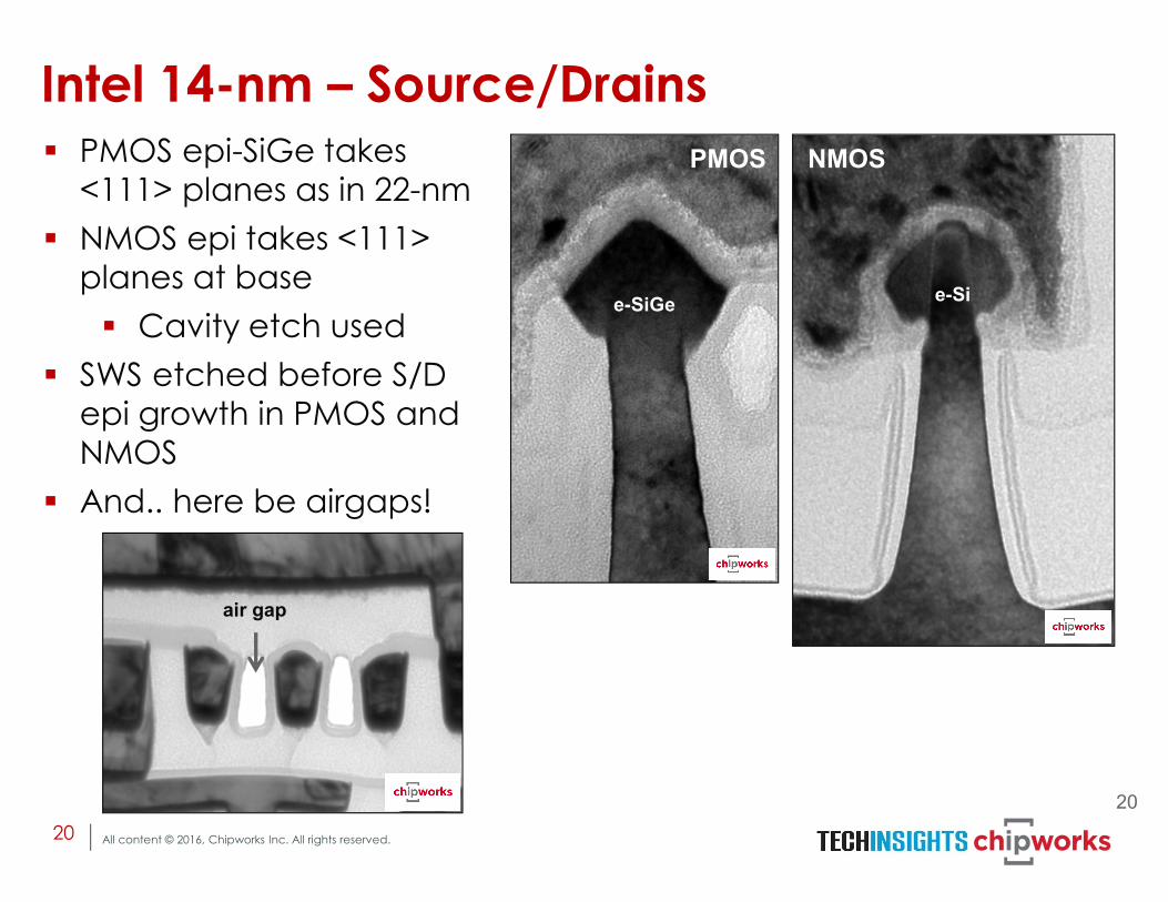
� PMOS epi-SiGe takes
<111> planes as in 22-nm
� NMOS epi takes <111>
planes at base
� Cavity etch used
� SWS etched before S/D
epi growth in PMOS and
NMOS
� And.. here be airgaps!
Intel 14-nm – Source/Drains
20
All content © 2016, Chipworks Inc. All rights reserved. 20
PMOS NMOS
e-SiGee-Si
air gap

21 All content © 2016, Chipworks Inc. All rights reserved.
Intel Solid-Source Diffusion Punchstopper
� Intel solved one of the biggest problems with bulk FinFETs,
putting in a self-aligned punchstop
� Allows a bulk FinFET to be undoped, assuming multi-WF RMG
� Reduces random doping variation
PSG Seal
BSG Seal
[3] Natarajan, et al. “A 14nm Logic Technology Featuring 2nd-
Generation FinFET , Air-Gapped Interconnects, Self-Aligned
Double Patterning and a 0.0588 µm2 SRAM cell size”, IEDM 2014

Intel 14 nm Atom “Cherrytrail” SoC
22 All content © 2016, Chipworks Inc. All rights reserved.

23 All content © 2016, Chipworks Inc. All rights reserved.
Intel 14 nm Atom “Cherrytrail” SoCPMOS NMOS� Logic transistors
same as Broadwell
microprocessor
� HV MOS similar fins
and 42 nm pitch with
nearly vertical
sidewalls and almost
flat top as LV MOS.
� HV CGP ~220 nm,
150 nm gate length
transistors� Thicker tox (4.0 nm – 4.5 nm), same
gate stack
� Merged SiGe epi and unmerged Si
epi
� Similar passives to 22-nm SoC

Samsung Exynos 7420 (14 nm Gate-Last HKMG FinFET Process)
24 All content © 2016, Chipworks Inc. All rights reserved.

25 All content © 2016, Chipworks Inc. All rights reserved.
� First generation tri-gate transistors, 2nd generation RMG process
� Minimum fin pitch ~48 nm, SADP litho to define fins
� CGP ~78 nm, single patterning plus cut mask (limit for 193 nm
immersion)
� Distinct fin isolation and well isolation
Samsung 14 nm finFETs

Samsung 14 nm PMOS Transistors
26 All content © 2016, Chipworks Inc. All rights reserved.
� MOLg ~28 nm, gate width ~80 nm
� Tox ~1.2 nm, thi-k ~1.3 nm
� Work-function materials similar to Intel/TSMC processes – PMOS is
TiN
� E-SiGe for stress, -> 40% Ge
PMOS
fin
SiO
HfO
gate metal sidewall
TiN PMOS WF
TiAlC
TiN liner

27 All content © 2016, Chipworks Inc. All rights reserved.
SiO
HfO
NMOS fin
gate metalTiN liner
TiAlC NMOS WF
interfacial TiN liner
� MOLg ~27 nm, gate width ~85 nm
� Fin width ~7 nm at half fin height
� Work-function materials similar to Intel/TSMC processes – NMOS
is TiAl + TiN (with C from ALD)
� Tox ~1.2 nm, thi-k ~1.3 nm
� Si epi for NMOS
Samsung 14 nm NMOS Transistors

Samsung 14 nm Source/Drains
28 All content © 2016, Chipworks Inc. All rights reserved.
� Epi in both cases takes <111> planes, and merged, unlike Intel
� Ti silicidation
� Significant etching of the PMOS epi during the contact etch,
dislocations in NMOS e-Si
PMOS NMOS

Apple APL1022 Application Processor (TSMC 16-nm FinFETHKMG Process)
29 All content © 2016, Chipworks Inc. All rights reserved.

30
Apple APL1022 Application Processor
All content © 2016, Chipworks Inc. All rights reserved.
PMOSNMOS
� First generation tri-gate transistors, 3rd generation RMG process
� Minimum fin pitch ~48 nm, CGP ~ 90 nm, SADP litho to define fins
� Functional gate height ~39 nm, gate width ~85 nm
� PMOS formed before NMOS; P + N WF layers in PMOS allows less room for W gate fill
PMOS
NMOS PMOS
NMOS

TSMC 16 nm PMOS Transistors
31 All content © 2016, Chipworks Inc. All rights reserved.
� Gates back-etched, capped with SiN
� MOLg ~30 nm, TiN WF layer, tox, thi-k ~1.3 nm
� Cavity etch for source/drains, backfilled with SiGe epi
� ~4 nm tox in I/O transistors, longer gate lengths allow W fill
dummy
gate
SiGe epi
dislocations
gate
STII/O transistor

32 All content © 2016, Chipworks Inc. All rights reserved.
gate dummy gate
Si epi
fin STI
� Gates back-etched, capped with SiN
� MOLg ~30 nm, WF layer TiAlCOF, tox, thi-k ~1.3 nm
� Cavity etch for source/drains, backfilled with Si epi
� ~3.5 nm tox in I/O transistors, longer gate lengths allow W fill
I/O transistor
TSMC 16 nm NMOS Transistors

33
TSMC 16 nm Source/Drains
All content © 2016, Chipworks Inc. All rights reserved.
PMOS NMOS
� PMOS e-SiGe has typical diamond shape, —> 55% Ge
� NMOS e-Si heavily gouged by contact etch
� Titanium used for silicidation
SiGe
epi
STISTI
Si
epi

34
Summary & Conclusions
All content © 2016, Chipworks Inc. All rights reserved.
� Definitely into the finFET era!
� Reviewed the last three 20/22-nm planar, 14/16 nm finFETtransistors
� We see a large degree of commonality in the final devices
� RMG gate dielectric high-k/oxide thicknesses all settled in the 1.0-1.3 nm range
� Fin profiles and dimensions, and gate widths, are similar
� Detail differences in gate stacks and capping layers.
� Gate lengths/ fin pitch dependent on final performance
� Foundries use Lg 28 – 30 nm, FP ~48 nm
� Intel uses ~22 nm, FP ~42 nm
� Double patterning (SADP) now standard
� 10 nm in 2017?

35
I would like to thank Chipworks’ laboratory staff and process analysts for all the hard work of analyzing these complex devices. They did a great job!
Acknowledgements
All content © 2016, Chipworks Inc. All rights reserved.