Molecules & Solids Harris Ch 9 Eisberg & Resnick Ch 13 & 14 RNave: Alison Baski: .
163
Molecules & Solids Harris Ch 9 Eisberg & Resnick Ch 13 & 14 RNave: http://hyperphysics.phy-astr.gsu.edu/hbase/solco n.html#solcon Alison Baski: http://www.courses.vcu.edu/PHYS661/pdf/01SolidSt ate041.ppt Carl Hepburn, “Britney Spear’s Guide to Semiconductor Physics”.
-
date post
21-Dec-2015 -
Category
Documents
-
view
233 -
download
6
Transcript of Molecules & Solids Harris Ch 9 Eisberg & Resnick Ch 13 & 14 RNave: Alison Baski: .

Molecules & Solids
Harris Ch 9
Eisberg & Resnick Ch 13 & 14
RNave: http://hyperphysics.phy-astr.gsu.edu/hbase/solcon.html#solcon
Alison Baski: http://www.courses.vcu.edu/PHYS661/pdf/01SolidState041.ppt
Carl Hepburn, “Britney Spear’s Guide to Semiconductor Physics”.
http://britneyspears.ac/lasers.htm

http://hyperphysics.phy-astr.gsu.edu/hbase/solcon.html#solcon

Harris Sections
• Bonding in Molecules (9.1-9.2)
• Rotation and Vibration in Molecules (9.3)
• Types of Solids & Crystals (9.4)
• Nearly Free-Electron Model (9.5)
• Conductors, Insulators, Semiconductors (9.6-9.9)
• Superconductivity (9.10)

A first look - Sharing Electrons
Harris 9.1

Isolated Atoms

Diatomic Molecule
Four Closely Spaced Atoms
valence band
conduction band

N closely-spaced Atoms
Harris 9.2
the level of interesthas the same nrg ineach separated atom

Solid of N atomsTwo atoms Six atoms
ref: A.Baski, VCU 01SolidState041.pptwww.courses.vcu.edu/PHYS661/pdf/01SolidState041.ppt

Solid composed of ~NA Na Atomsas fn(R)
1s22s22p63s1

Sodium Bands vs Separation
Rohlf Fig 14-4 and Slater Phys Rev 45, 794 (1934)

Copper Bands vs Separation
Rohlf Fig 14-6 and Kutter Phys Rev 48, 664 (1935)
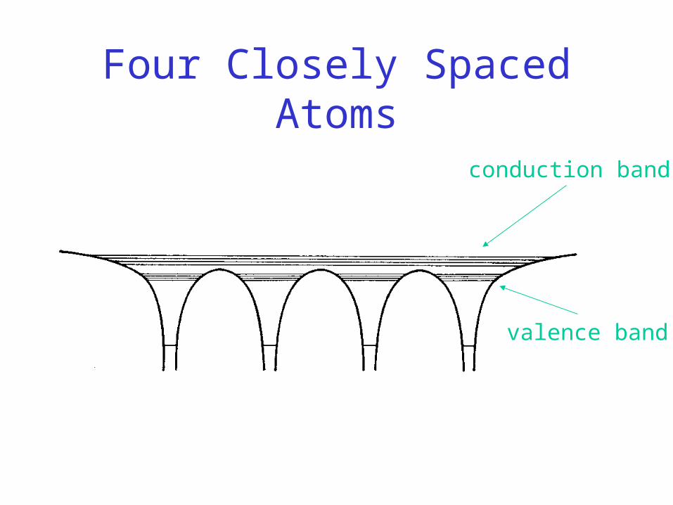
Differences down a column in the Periodic Table: IV-A Elements
Sandin
same valenceconfig

The 4A Elements

Bonding in Molecules
Harris 9.2

Bondinghttp://hyperphysics.phy-astr.gsu.edu/hbase/chemical/chemcon.html#c1
R Nave, Georgia State Univ

Chemical Bondinghttp://hyperphysics.phy-astr.gsu.edu/hbase/chemical/bondcon.html#c1
R Nave, Georgia State Univ

Ionic Bonds
RNave, GSU at http://hyperphysics.phy-astr.gsu.edu/hbase/chemical/bond.html#c4


Ioniz Electron
Affinity
Coul
Attraction
Pauli
Repulsion
Energy
Balance
NaCl 5.14 -3.62 -6.10 0.31 -4.27
NaF 5.14 -3.41 -7.46 0.35 -5.34
KCl 4.34 -3.62 -5.39 0.19 -4.49
HH 13.6 -0.76

Ionic Bonds

Covalent Bonds
RNave, GSU at http://hyperphysics.phy-astr.gsu.edu/hbase/chemical/bond.html#c4

Covalent Bonding SYM ASYMspatial spin
ASYM SYMspatial spin
Harris

Covalent Diatomic Level Diagram
Harris Fig 9.8

Covalent Bonding
Stot = 1
not really parallel, but spin-symmetric
not really anti, but spin-asym
Stot = 0
E&R

Covalent
Solid of N atomsTwo atoms Six atoms
ref: A.Baski, VCU 01SolidState041.pptwww.courses.vcu.edu/PHYS661/pdf/01SolidState041.ppt

Interesting Pictures

Covalent Bonding with p-orbitals
Harris 9.9 & 9.10

Bonding with p-orbitals
Harris 9.11

Bonding Dissimilar Atoms-- broken symmetry
H 9.14 & Table 9.1

Ionic vs Covalent Bond Properties
• Ionic Characteristics– Crystalline solids
– High melting & boiling point
– Conduct electricity when melted
– Many soluble in water, but not in non-polar liquids
• Covalent Characteristics– Gases, liquids, non-crystalline
solids
– Low melting & boiling point
– Poor conductors in all phases
– Many soluble in non-polar liquids but not water

Ionic Bonds
RNave, GSU at http://hyperphysics.phy-astr.gsu.edu/hbase/chemical/bond.html#c4

Ionic Bonds

Ionic Bonding
RNave, Georgia State Univ at hyperphysics.phy-astr.gsu.edu/hbase/molecule

Covalent Bonds
RNave, GSU at http://hyperphysics.phy-astr.gsu.edu/hbase/chemical/bond.html#c4

Covalent Bonding SYM ASYMspatial spin
ASYM SYMspatial spin
space-symmetric tend to be closer
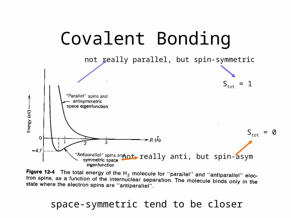
Covalent Bonding
Stot = 1
not really parallel, but spin-symmetric
not really anti, but spin-asym
Stot = 0
space-symmetric tend to be closer

Molecular ExcitationsRotation, Vibration, Electric
Harris 9.3

Rotational Spectra
)1(22
1
2
1~
222 rr
IIIKErot
R
rotational A.M.moment of inertia

Rotation

Rotation

Rotational Spectra

Vibration
Molecule“Spring Const”
( N/m )
HF 970
HCl 480
HBr 410
Hi 320
CO 1860
NO 1530

Vibration (in an Electronic state)

Ocean Optics: Nitrogen N2
~ 0.3 eV
~ 0.4 eV

Electronic + Vibration

Electronic + Vibration + Rotation
2.656 eV2.550 eV
electronic excitation gap
vibrational excitation gaps

Electronic + Vibration + Rotation
2.656 eV
electronic excitation gap
vibrational excitation gaps
Vibrational WellVibrational Well
depth ~ 0.063 eV

Electronic, Vibration, RotationElectronic ~ optical & UV
~ 1 – 3 eV
Vibration ~ IR ~ 10ths of eV
Rotation ~ microwave ~ 1000ths of eV
Harris 9.24

Electronic, Vibration, RotationElectronic ~ optical & UV
~ 1 – 3 eV
Vibration ~ IR ~ 10ths of eV
Rotation ~ microwave ~ 1000ths of eV

Electronic + Vibration + Rotation
2.656 eV2.550 eV
electronic excitation gap
vibrational excitation gaps

** + Vibration + Rotation
IN A DIATOMIC MOLECULEbecause a photon has one unit of
angular momentum,the rotational quantum number
must change(vib is not angular motion)
r = 0 not allowed

** + Vibration + Rotation

Ocean Optics: Nitrogen N2
~ 0.3 eV
~ 0.4 eV


Some Molecular ConstantsMolecule Equilibrium
Distance
Ro (Å)
Dissociation NRG
Do (eV)
Vibrational freq
v a (cm-1)
Moment of Inertia
Bb (cm-1)
H2+ 1.06 2.65 2297 29.8
H2 0.742 4.48 4395 60.8
O2 1.21 5.08 1580 1.45
N2 1.09 9.75 2360 2.01
CO 1.13 9.60 2170 1.93
NO 1.15 5.3 1904 1.70
HCl 1.28 4.43 2990 10.6
NaCl 2.36 4.22 365 0.190
Notes: a) vibrational frequency in table is given as f / c b) moment of inertia in table is given as hbar2/(2I) / hc

Types of Solids
Harris 9.4

TYPES OF SOLIDS (ER 13.2)
CRYSTALINE BINDING
• molecular
• ionic
• covalent
• metallic
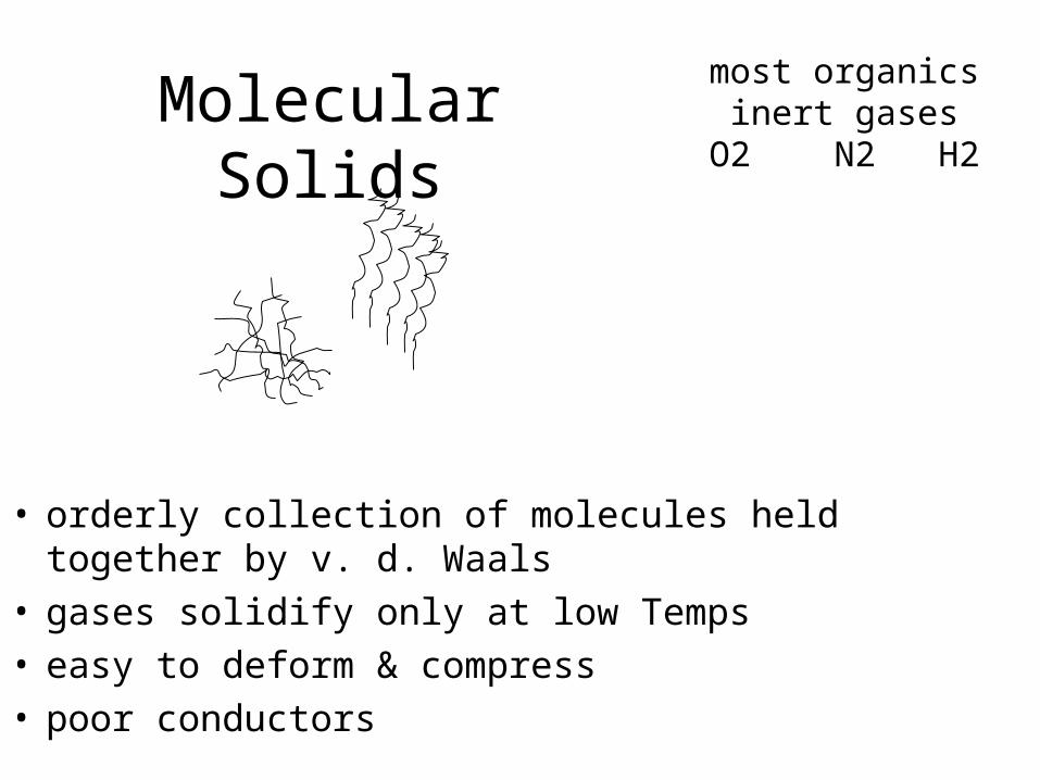
Molecular Solids
• orderly collection of molecules held together by v. d. Waals• gases solidify only at low Temps• easy to deform & compress• poor conductors
most organicsinert gases
O2 N2 H2

Ionic Solids• individ atoms act like closed-shell, spherical, therefore binding not so directional• arrangement so that minimize nrg for size of atoms
• tight packed arrangement poor thermal conductors• no free electrons poor electrical conductors• strong forces hard & high melting points• lattice vibrations absorb in far IR• to excite electrons requires UV, so ~transparent visible
NaClNaIKCl

Covalent Solids
• 3D collection of atoms bound by shared valence electrons
• difficult to deform because bonds are directional• high melting points (b/c diff to deform)• no free electrons poor electrical conductors• most solids adsorb photons in visible opaque
Ge Si
diamond

Metallic Solids
• (weaker version of covalent bonding)• constructed of atoms which have very weakly
bound outer electron• large number of vacancies in orbital (not enough
nrg available to form covalent bonds)• electrons roam around (electron gas )• excellent conductors of heat & electricity• absorb IR, Vis, UV opaque
Fe Ni Co
config dhalf full


Free-Electron Model and
Band Formation
Harris 9.5

‘Free-Electron’ Models
• Free Electron Model • Nearly-Free Electron Model
– Version 1 – SP221– Version 2 – SP324a– Version 3 – SP324b
• .
*********************************************************

Free-Electron Model (ER13-5)
m
k
m
p
22
222
classical description

Problems with Free Electron Model
* * * * * * * * * * * * * * * * * * * * * * * * * * * *
1) Bragg reflection2) .3) .

Other Problems with the Free Electron Model
• graphite is conductor, diamond is insulator• variation in colors of x-A elements• temperature dependance of resistivity• resistivity can depend on orientation of crystal & current I direction• frequency dependance of conductivity• variations in Hall effect parameters• resistance of wires effected by applied B-fields
• .• .• .

Nearly-Free Electron Modelversion 1 – SP221

Nearly-Free Electron Modelversion 1 – SP221
2/2
2/k
a
2/k
2/2
2/k
a

Nearly-Free Electron Modelversion 1 – SP221
2/2
2/k
a
2/k
2/2
2/k
a

Nearly-Free Electron Model version 2 – SP324a

Nearly-Free Electron Model version 2 – SP324a
• Bloch Theorem
• Special Phase Conditions, k = +/- m /a
• the Special Phase Condition k = +/- /a
This treatment assumes that when a reflection occurs, it is 100%.

(x) ~ u e i(kx-t)
(x) ~ u(x) e i(kx-t)
~~~~~~~~~~
amplitude
In reality, lower energy waves are sensitive to the lattice:
Amplitude varies with location
u(x) = u(x+a) = u(x+2a) = ….
Bloch’sTheorem
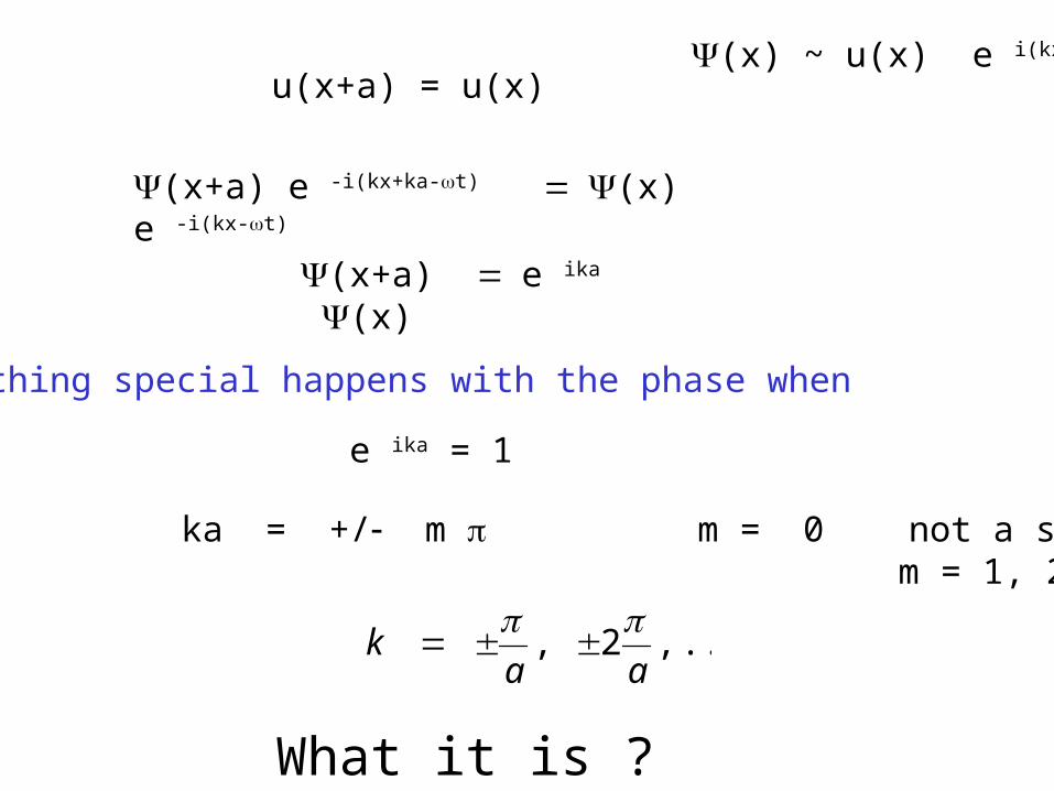
u(x+a) = u(x)
(x+a) e -i(kx+ka-t) (x) e -i(kx-t)
(x) ~ u(x) e i(kx-t)
(x+a) e ika (x)
Something special happens with the phase when
e ika = 1
ka = +/ m m = 0 not a surprise m = 1, 2, 3, …
...,2,aa
k
What it is ?

ak
Consider a set of waves with +/ k-pairs, e.g.
k = + /a moves k = /a moves
This defines a pair of waves moving right & left
Two trivial ways to superpose these waves are:
+ ~ e ikx + e ikx ~ e ikx e ikx
+ ~ 2 cos kx ~ 2i sin kx

+ ~ 2 cos kx ~ 2i sin kx
Kittel
+|2 ~ 4 cos2 kx |2 ~ 4 sin2 kx

Free-electron Nearly Free-electron
Kittel
Discontinuities occur because the lattice is impacting the movement of electrons.

Effective Mass m*
A method to force the free electron model to work in the situations where
there are complications
*2
22
m
k
free electron KE functional form

Effective Mass m* -- describing the balance between applied ext-E and lattice site reflections
2
2
2
1
*
1
km
m* a = Fext
q Eext

No distinction between m & m*, m = m*, “free electron”, lattice structure does not apply additional restrictions on motion.
m = m*
greater curvature, 1/m* > 1/m > 0, m* < m net effect of ext-E and lattice interaction provides additional acceleration of electrons
greater |curvature| but negative,net effect of ext-E and lattice interaction de-accelerates electrons #1
At inflection pt
1)
2)

*
2222
22 m
k
m
k latticefromonperturbatiapply
Another way to look at the discontinuities
Shift up implies effective mass has decreased, m* < m, allowing electrons to increase their speed and join faster electrons in the band.The enhanced e-lattice interaction speeds up the electron.
Shift down implies effective mass has increased, m* > m, prohibiting electrons from increasing their speed and makingthem become similar to other electrons in the band.The enhanced e-lattice interaction slows down the electron

From earlier: Even when above barrier, reflection and transmission coefficients can increase and decrease depending upon the energy.

change in motiondue to reflections is more significant
than change in motiondue to applied field
change in motion
due to applied field enhanced by change in reflection coefficients

Nearly-Free Electron Model version 3

From earlier:Even when above barrier, reflection and transmission coefficients can increase and decrease depending upon the energy.
Nearly-Free Electron Model version 3

Nearly-Free Electron Model version 3
à la Ashcroft & Mermin, Solid State Physics
This treatment recognizes that the reflections of electron waves off lattice sites can be more complicated.

A reminder:

Waves from the left behave like:
iKxiKx
leftthefrom ere
iKx
leftthefrom et
m
K
2
22
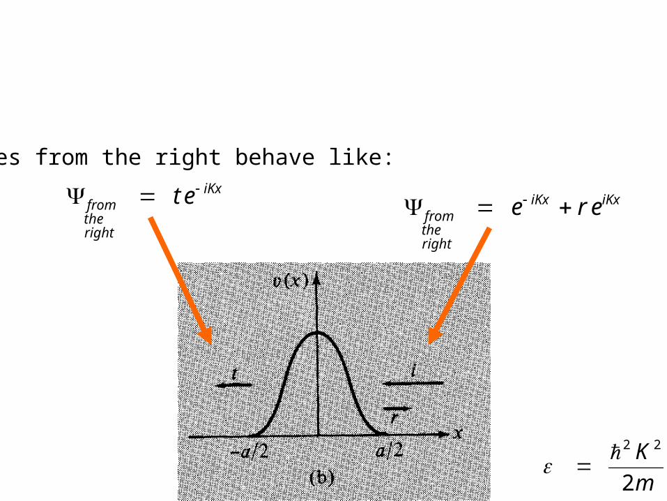
Waves from the right behave like:
iKxiKx
rightthefrom ere
iKx
rightthefrom et
m
K
2
22

rightleftsum BA
Bloch’s Theorem defines periodicity of the wavefunctions:
xeax sumika
sum
xeax sumika
sum
unknown weights
Related toLattice spacing
xeax sumika
sum xeax sumika
sum
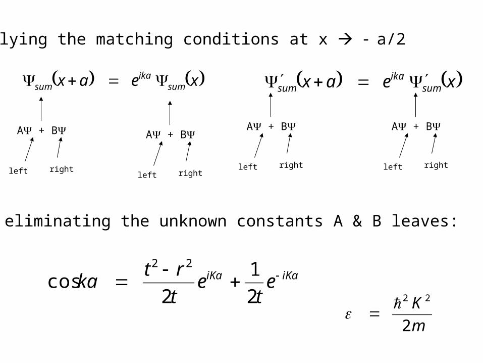
Applying the matching conditions at x a/2
A + B
left right
A + B
left right
A + B
left right
A + B
left right
iKaiKa et
et
rtka
2
1
2cos
22
m
K
2
22
And eliminating the unknown constants A & B leaves:
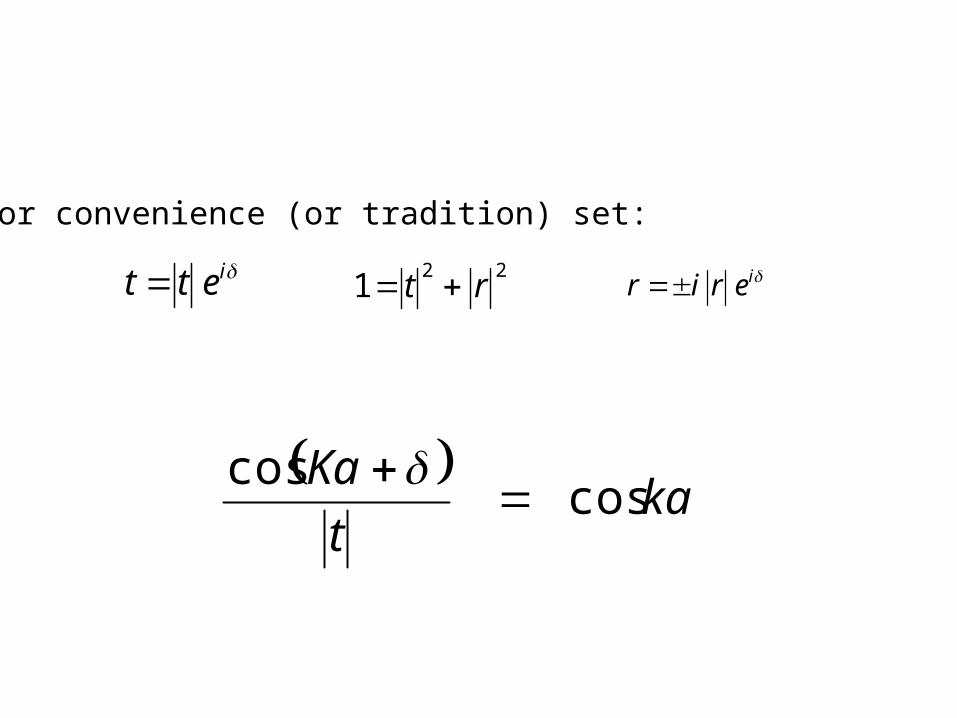
For convenience (or tradition) set:
221 rt iett ierir
ka
t
Kacos
cos

-2
-1.5
-1
-0.5
0
0.5
1
1.5
2
0 1 2 3 4 5 6 7 8
a
valu
e
COS(electron)
COS(lattice)
ka
t
Kacos
cos
Related topossible
Lattice spacings
Related toEnergy
m
K
2
22
allowed solution regions

ka
t
Kacos
cos
Related topossible
Lattice spacings
Related toEnergy
m
K
2
22
allowed solution regions

allo
wed
sol
utio
n re
gion
s

allo
wed
sol
utio
n re
gion
s

Conductors, Insulators, Semiconductors
Harris 9.6-9.9

The transistor is the result of "reverse engineering" of the electronic remains of the UFO that landed in Roswell in 1947?
http://www.porticus.org/bell/belllabs_transistor.html
http://www.subversiveelement.com/Roswell_Reverse_Engineering_Shul.html

Band Spacingsin
Insulators & Conductors
electrons free to roam
electrons confined to small region
RNave: http://hyperphysics.phy-astr.gsu.edu/hbase/solcon.html#solcon

Conductors & Insulators at T=0
H9.35a

Conductors & Insulators at T>0
H9.35b

Fermi Distribution for a selected F
0
0.5
1
1.5
0 1 2 3 4
Energy
Pro
bab
ilit
y o
f an
en
erg
y o
ccu
rin
g
(no
t n
orm
alized
)
T=0
1000
5000
1
1)(
/)( kTFe
n

How does one choose/know F ?
If in unfilled band, F is energy of highest energy electrons at T=0.
If in filled band with gap to next band, F is at the middle of gap.

FermionsT=0
RNave: http://hyperphysics.phy-astr.gsu.edu/hbase/solcon.html#solcon

Fermions T > 0

How Many Electrons
Get Promoted?
9.37
f
dDN tot
0
)(
2/
)()(gapf
dDNN fermiexcited
Assume D() ~ constant in band

How Many Electrons Get Promoted?
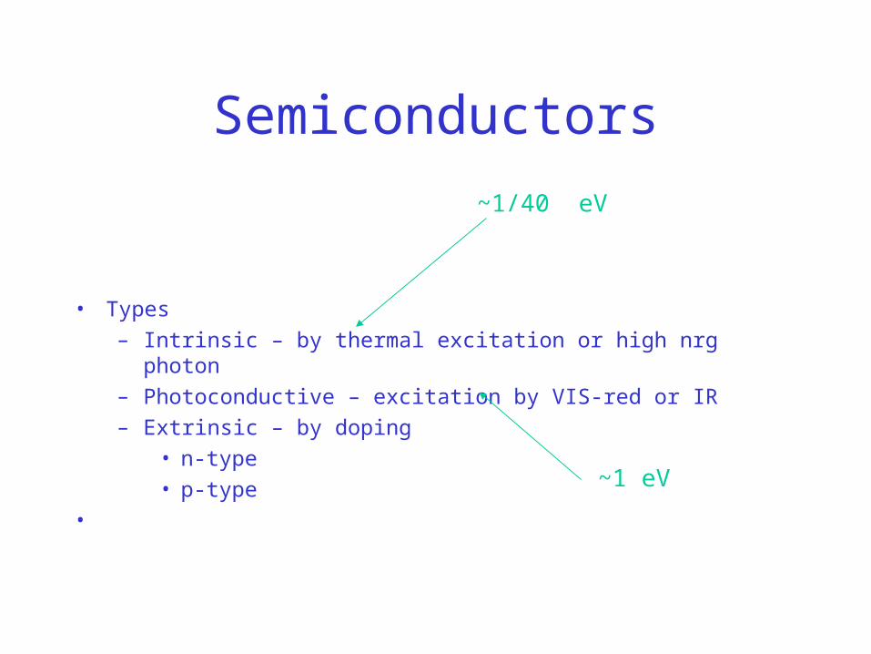
Semiconductors
• Types
– Intrinsic – by thermal excitation or high nrg photon
– Photoconductive – excitation by VIS-red or IR
– Extrinsic – by doping
• n-type
• p-type
• ~1 eV
~1/40 eV

Intrinsic Semiconductors
Silicon
Germanium
RNave: http://hyperphysics.phy-astr.gsu.edu/hbase/solcon.html#solcon

Electrons & Holes
2
2
2
1
*
1
km
9.409.41
m* ‘q’ direction I=nqvdA
Bot-band electron + opp with
Top-band electron with opp
m* a = Fext = ‘q’Eext
Eext

Doped Semiconductorslattice
p-type dopants n-type dopants

5A in 4A lattice
3A in 4A lattice
5A doping in a 4A lattice

Bands in n-doped Semiconductor
9.44

Bands in p-doped Semiconductor
9.45

5A in 4A lattice 3A in 4A lattice

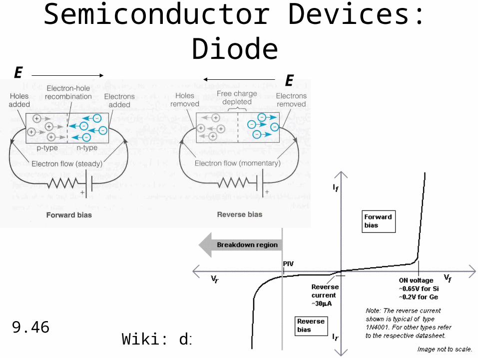
Semiconductor Devices: Diode
9.46Wiki: diode
EE

Semiconductor Devices: Diode9.47

Semiconductor Devices: Diode9.48

Semiconductor Devices: Diode9.53

PN Diode Junction with bias
http://jas.eng.buffalo.edu/education/pn/biasedPN/index.html
C.R.Wie, SUNY-Buffalo
Applet demonstrating charge flow in valence & conduction bands in a diode.
Found by Ryan Pifer ‘09

Semiconductor Devices: Transistor
9.49


Superconductivity
Harris 9.10

R Nave: http://hyperphysics.phy-astr.gsu.edu/hbase/solids/supcon.html#c1
Temperature Dependence of Resistivity
Joe Eck: superconductors.org

Temperature Dependence of Resistivity
A
LR

• Conductors– Resistivity increases with increasing Temp Temp but same # conduction e-’s
• Semiconductors & Insulators– Resistivity decreases with increasing Temp
Temp but more conduction e-’s

First observed Kamerlingh Onnes 1911

Superconductors.org Only in nanotubes
Note: The best conductors & magnetic materials tend not to be superconductors (so far)

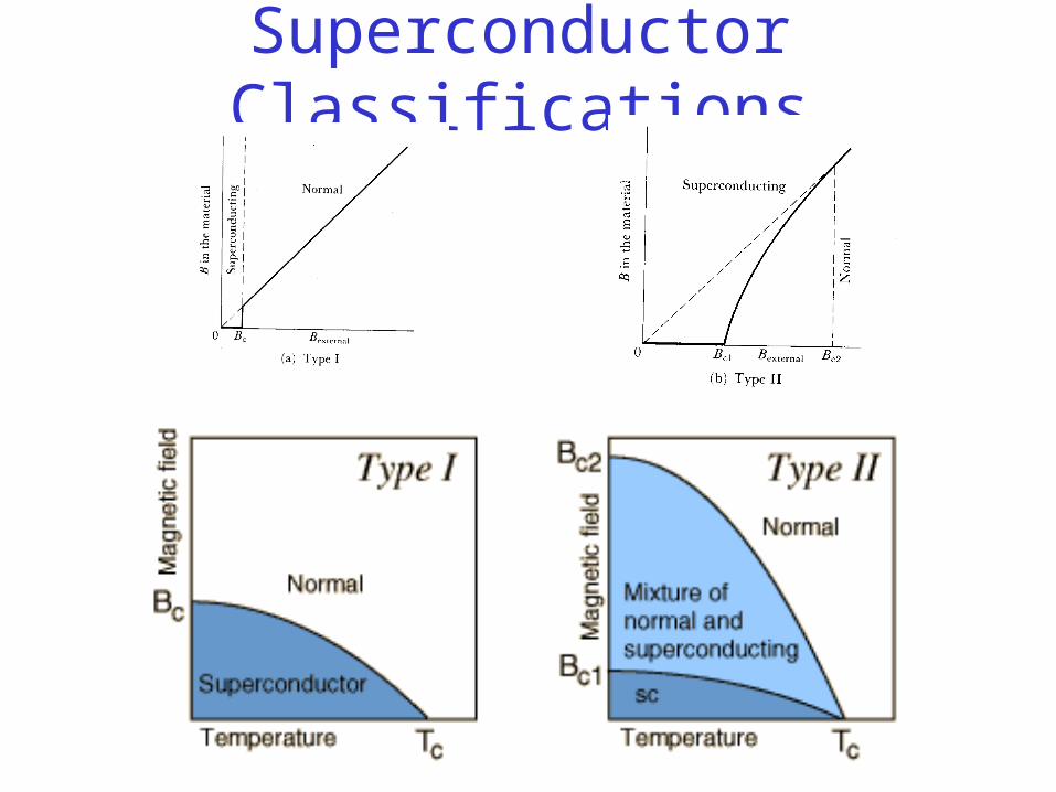
Superconductor Classifications• Type I
– tend to be pure elements or simple alloys– = 0 at T < Tcrit
– Internal B = 0 (Meissner Effect)– At jinternal > jcrit, no superconductivity– At Bext > Bcrit, no superconductivity– Well explained by BCS theory
• Type II– tend to be ceramic compounds– Can carry higher current densities ~ 1010 A/m2
– Mechanically harder compounds– Higher Bcrit critical fields– Above Bext > Bcrit-1, some superconductivity
Superconductor Classifications
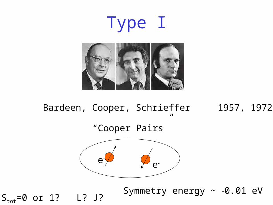
Type I
Bardeen, Cooper, Schrieffer 1957, 1972
“Cooper Pairs”
Symmetry energy ~ 0.01 eVQ: Stot=0 or 1? L? J?
e e

Sn 230 nmAl 1600Pb 83Nb 38
Best conductors best ‘free-electrons’ no e – lattice interaction not superconducting
Popular Bad Visualizations:
Pairs are related by momentum ±p, NOT position.
correlation lengths

More realistic 1-D billiard ball picture:
Cooper Pairs are ±k sets
Furthermore:
“Pairs should not be thought of as independent particles” -- Ashcroft & Mermin Ch 34

• Experimental Support of BCS Theory– Isotope Effects
– Measured Band Gaps corresponding to Tcrit predictions
– Energy Gap decreases as Temp Tcrit
– Heat Capacity Behavior

Normal Conductor
Semiconductor or
Superconductor

Another fact about Type I:
-- Interrelationship of Bcrit and Tcrit

Type II
Q: does BCS apply ?
mixed normal/super
Yr Composition Tc
May
2006InSnBa4Tm4Cu6O18+ 150
2004 Hg0.8Tl0.2Ba2Ca2Cu3O8.33 138
1986 (La1.85Ba.15)CuO4 30
YBa2Cu3O7 93

actual ~ 8 m
Sandin

Type II – mixed phases
Q: does BCS apply ?
fluxon

Y Ba2 Cu3 O7 crystalline
La2-x Bax Cu O2 solid solution
may control the electronic config of the conducting layer

Another fact about Type II:
-- Interrelationship of Bcrit and Tcrit

ApplicationsOR
Other Features of Superconductors
http://superconductors.org/Uses.htm

Meissner Effect

Magnetic Levitation – Meissner Effect
Q: Why ?
Kittel states this explusion effectis not clearly directly connected to the = 0 effects

Magnetic Levitation – Meissner Effect
MLX01 Test Vehicle
2003 581 km/h 361 mph2005 80,000+ riders2005 tested passing trains at relative 1026 km/h
http://www.rtri.or.jp/rd/maglev/html/english/maglev_frame_E.html

MagLev in Shanghai

Maglev in Germany (sc? idi)
32 km track550,000 km since 1984Design speed 550 km/h
NOTE(061204): I’m not so sure this track is superconducting. The MagLev planned for the Munich area will be. France is also thinking about a sc maglev.

Maglev Frog
A live frog levitates inside a 32 mm diameter vertical bore of a Bitter solenoid in a magnetic field of about 16 Tesla at the Nijmegen High Field Magnet Laboratory.
http://www.hfml.ru.nl/pics/Movies/frog.mpg

Josephson Junction~ 2 nm

Recall: Aharonov-Bohm Effect-- from last semester
affects the phase of a wavefunction
Source B/)( 2~ reApie
/)( 1~ reApie
/~~ ipxikx ee
A

SQUIDsuperconducting quantum interference device
leftioe
~ rightioe
~
o

ioe ~
)(locationfn
BBohmAharonov
loop
qndl
2
qnB
2
2151007.2)2(
2mTelsa
e
Add up change in flux as go around loop

Typical B fields
(Tesla) (# flux quanta)

MAGSAFE will be able to locate targets without flying close to the surface.Image courtesy Department of Defence.
http://www.csiro.au/science/magsafe.html
Finding 'objects of interest' at sea with MAGSAFE
MAGSAFE is a new system for locating and identifying submarines.
Operators of MAGSAFE should be able to tell the range, depth and bearing of a target, as well as where it’s heading, how fast it’s going and if it’s diving.
Building on our extensive experience using highly sensitive magnetic sensors known as Superconducting QUantum Interference Devices (SQUIDs) for minerals exploration, MAGSAFE harnesses the power of three SQUIDs to measure slight variations in the local magnetic field.
MAGSAFE has higher sensitivity and greater immunity to external noise than conventional Magnetic Anomaly Detector (MAD) systems. This is especially relevant to operation over shallow seawater where the background noise may 100 times greater than the noise floor of a MAD
instrument.

Phillip Schmidt etal. Exploration Geophysics 35, 297 (2004).
http://www.csiro.au/science/magsafe.html

Arian Lalezari

SQUID2 nm
1014 T SQUID thresholdHeart signals 10 10 TBrain signals 10 13 T

• Fundamentals of superconductors:– http://www.physnet.uni-hamburg.de/home/vms/reimer/htc/pt3.html
• Basic Introduction to SQUIDs:– http://www.abdn.ac.uk/physics/case/squids.html
• Detection of Submarines
– http://www.csiro.au/science/magsafe.html • Fancy cross-referenced site for Josephson Junctions/Josephson:
– http://en.wikipedia.org/wiki/Josephson_junction– http://en.wikipedia.org/wiki/B._D._Josephson
• SQUID sensitivity and other ramifications of Josephson’s work:– http://hyperphysics.phy-astr.gsu.edu/hbase/solids/squid2.html
• Understanding a SQUID magnetometer:– http://hyperphysics.phy-astr.gsu.edu/hbase/solids/squid.html#c1
• Some exciting applications of SQUIDs:– http://www.lanl.gov/quarterly/q_spring03/squid_text.shtml

• Relative strengths of pertinent magnetic fields– http://www.physics.union.edu/newmanj/2000/SQUIDs.htm
• The 1973 Nobel Prize in physics– http://nobelprize.org/physics/laureates/1973/
• Critical overview of SQUIDs– http://homepages.nildram.co.uk/~phekda/richdawe/squid/popular/
• Research Applications– http://boojum.hut.fi/triennial/neuromagnetic.html
• Technical overview of SQUIDs:– http://www.finoag.com/fitm/squid.html– http://www.cmp.liv.ac.uk/frink/thesis/thesis/node47.html

Redraw LHS
Sn 230 nmAl 1600Pb 83Nb 38
Best conductors best ‘free-electrons’ no e – lattice interaction not superconducting