Molecular Electronics - Nanotechnology and Emerging Technologies
Upload
mohamed-salehCategory
view
48download
0description
January 12, 2010 11:27 World Scientific Book - 9in x 6in book
Preface
The trend in the miniaturization of electronic devices has naturally ledto the question of whether or not it is possible to use single moleculesas active elements in nanocircuits for a variety of applications. The re-cent developments in nanofabrication techniques have made possible theold dream of contacting individual molecules and exploring their electronictransport properties. Moreover, it has been shown that molecules can in-deed mimic the behavior of some of today’s microelectronic components,and even strategies to interconnect molecular devices have already beendeveloped. These achievements have given rise to what is nowadays knownas Molecular Electronics. There are still many problems and challengesto be faced to make this novel electronics a viable technology, but theexploration of molecular-scale circuits has already led to the discovery ofmany fundamental e!ects. In this sense, molecular electronics has becomea new interdisciplinary field of science, in which knowledge from traditionaldisciplines like physics, chemistry, engineering and biology is combined tounderstand the electrical and thermal conduction at the molecular scale.
This book provides a comprehensive overview of the rapidly developingfield of molecular electronics. It focuses on our present understanding ofthe electrical conduction in single-molecule circuits and presents a thoroughintroduction to the experimental techniques and the theoretical concepts.To be precise, our goal in this monograph is two-fold. On the one hand, wewant to provide a true textbook for advanced undergraduate and graduatestudents both in physics and chemistry who are interested in the field ofmolecular electronics or nanoelectronics in general. Our idea is to takea student with a good background in quantum mechanics all the way tobe able to follow the specialized literature in molecular electronics or tostart working in this field. On the other hand, we also want provide a
vii
January 12, 2010 11:27 World Scientific Book - 9in x 6in book
viii Molecular Electronics: An Introduction to Theory and Experiment
thorough review of the recent activities in molecular electronics from whichnewcomers and specialists in the field can benefit.
Bearing these goals in mind, this book has been written in a self-contained and unified way. It contains four parts that can be read indepen-dently. In the first two ones we review the basic experimental techniquesand the main theoretical concepts concerning the electronic transport inatomic-scale junctions. These two parts are meant to be textbook materialfor an advanced course in molecular electronics. In particular, we have in-cluded a collection of exercises at the end of most chapters, which in manycases are motivated by recent experiments in the field. On the other hand,Part 3 contains two chapters in which we describe at an introductory levelthe physics of metallic atomic-size contacts and we also point out some ofthe remaining challenges and open problems in this context. Finally, Part4 is devoted to the electrical and thermal transport in molecular circuits,with special emphasis on single-molecule junctions. Here, we do not onlyreview the recent activities in the field of molecular electronics, but we alsointroduce the addressed topics at a basic level. In this sense, we have oftenincluded unpublished material and additional exercises to help the readerto gain a deeper insight into the fundamental concepts involved in the fieldof molecular electronics.1
We have tried to cover in this monograph as many aspects of molecularelectronics as possible, but obviously the selection is limited for space rea-sons and it reflects unavoidably our own research interests. We also wantto apologize with those authors that feel that their contribution was notproperly highlighted in the review part of this monograph, but it is by nowimpossible to include all the huge amount of work done in this field. Fi-nally, we just hope to have achieved, at least partially, the goal that trulymotivated the writing of this book, namely the sincere will to provide auseful book for the new generation of researchers that should consolidatemolecular electronics as a solid pillar of the emerging nanoscience.
1See section 1.3 for a more detailed description of the structure and scope of the book.
January 12, 2010 11:27 World Scientific Book - 9in x 6in book
Contents
Preface vii
Acknowledgments ix
Brief history of the field and experimental tech-niques 1
1. The birth of molecular electronics 3
1.1 Why molecular electronics? . . . . . . . . . . . . . . . . . 5
1.2 A brief history of molecular electronics . . . . . . . . . . . 6
1.3 Scope and structure of the book . . . . . . . . . . . . . . 14
2. Fabrication of metallic atomic-size contacts 19
2.1 Introduction . . . . . . . . . . . . . . . . . . . . . . . . . . 19
2.2 Techniques involving the scanning electron microscope(STM) . . . . . . . . . . . . . . . . . . . . . . . . . . . . . 19
2.3 Methods using atomic force microscopes (AFM) . . . . . 21
2.4 Contacts between macroscopic wires . . . . . . . . . . . . 22
2.5 Transmission electron microscope . . . . . . . . . . . . . . 23
2.6 Mechanically controllable break junctions (MCBJ) . . . . 24
2.7 Electromigration technique . . . . . . . . . . . . . . . . . 31
2.8 Electrochemical methods . . . . . . . . . . . . . . . . . . . 35
2.9 Recent developments . . . . . . . . . . . . . . . . . . . . . 37
2.10 Electronic transport measurements . . . . . . . . . . . . . 38
2.11 Exercises . . . . . . . . . . . . . . . . . . . . . . . . . . . 43
xi
January 12, 2010 11:27 World Scientific Book - 9in x 6in book
xii Molecular Electronics: An Introduction to Theory and Experiment
3. Contacting single molecules: Experimental techniques 45
3.1 Introduction . . . . . . . . . . . . . . . . . . . . . . . . . . 45
3.2 Molecules for Molecular Electronics . . . . . . . . . . . . . 46
3.2.1 Hydrocarbons . . . . . . . . . . . . . . . . . . . . 47
3.2.2 All carbon materials . . . . . . . . . . . . . . . . . 50
3.2.3 DNA and DNA derivatives . . . . . . . . . . . . . 51
3.2.4 Metal-molecule contacts: anchoring groups . . . . 52
3.2.5 Conclusions: molecular functionalities . . . . . . . 52
3.3 Deposition of molecules . . . . . . . . . . . . . . . . . . . 53
3.4 Contacting single molecules . . . . . . . . . . . . . . . . . 55
3.4.1 Electromigration technique . . . . . . . . . . . . . 56
3.4.2 Molecular contacts using the transmission electronmicroscope . . . . . . . . . . . . . . . . . . . . . . 58
3.4.3 Gold nanoparticle dumbbells . . . . . . . . . . . . 59
3.4.4 Scanning probe techniques . . . . . . . . . . . . . 60
3.4.5 Mechanically controllable break-junctions (MCBJs) 64
3.5 Contacting molecular ensembles . . . . . . . . . . . . . . . 66
3.5.1 Nanopores . . . . . . . . . . . . . . . . . . . . . . 66
3.5.2 Shadow masks . . . . . . . . . . . . . . . . . . . . 68
3.5.3 Conductive polymer electrodes . . . . . . . . . . . 69
3.5.4 Microtransfer printing . . . . . . . . . . . . . . . . 70
3.5.5 Gold nanoparticle arrays . . . . . . . . . . . . . . 71
3.6 Exercises . . . . . . . . . . . . . . . . . . . . . . . . . . . 73
Theoretical background 75
4. The scattering approach 77
4.1 Introduction . . . . . . . . . . . . . . . . . . . . . . . . . . 77
4.2 From mesoscopic conductors to atomic-scale junctions . . 79
4.3 Conductance is transmission: Heuristic derivation of theLandauer formula . . . . . . . . . . . . . . . . . . . . . . . 81
4.4 Penetration of a potential barrier: Tunnel e!ect . . . . . . 83
4.5 The scattering matrix . . . . . . . . . . . . . . . . . . . . 88
4.5.1 Definition and properties of the scattering matrix 88
4.5.2 Combining scattering matrices . . . . . . . . . . . 91
4.6 Multichannel Landauer formula . . . . . . . . . . . . . . . 92
January 12, 2010 11:27 World Scientific Book - 9in x 6in book
Contents xiii
4.6.1 Conductance quantization in 2DEG: Landauer for-mula at work . . . . . . . . . . . . . . . . . . . . . 97
4.7 Shot Noise . . . . . . . . . . . . . . . . . . . . . . . . . . . 99
4.8 Thermal transport and thermoelectric phenomena . . . . 104
4.9 Limitations of the scattering approach . . . . . . . . . . . 106
4.10 Exercises . . . . . . . . . . . . . . . . . . . . . . . . . . . 107
5. Introduction to equilibrium Green’s function techniques 111
5.1 The Schrodinger and Heisenberg pictures . . . . . . . . . 112
5.2 Green’s functions of a noninteracting electron system . . . 1135.3 Application to tight-binding Hamiltonians . . . . . . . . . 118
5.3.1 Example 1: A hydrogen molecule . . . . . . . . . 118
5.3.2 Example 2: Semi-infinite linear chain . . . . . . . 122
5.3.3 Example 3: A single level coupled to electrodes . 124
5.4 Green’s functions in time domain . . . . . . . . . . . . . . 1285.4.1 The Lehmann representation . . . . . . . . . . . . 131
5.4.2 Relation to observables . . . . . . . . . . . . . . . 134
5.4.3 Equation of motion method . . . . . . . . . . . . 136
5.5 Exercises . . . . . . . . . . . . . . . . . . . . . . . . . . . 139
6. Green’s functions and Feynman diagrams 143
6.1 The interaction picture . . . . . . . . . . . . . . . . . . . . 144
6.2 The time-evolution operator . . . . . . . . . . . . . . . . . 1466.3 Perturbative expansion of causal Green’s functions . . . . 148
6.4 Wick’s theorem . . . . . . . . . . . . . . . . . . . . . . . . 149
6.5 Feynman diagrams . . . . . . . . . . . . . . . . . . . . . . 151
6.5.1 Feynman diagrams for the electron-electron inter-action . . . . . . . . . . . . . . . . . . . . . . . . . 152
6.5.2 Feynman diagrams for an external potential . . . 157
6.6 Feynman diagrams in energy space . . . . . . . . . . . . . 158
6.7 Electronic self-energy and Dyson’s equation . . . . . . . . 162
6.8 Self-consistent diagrammatic theory: The Hartree-Fockapproximation . . . . . . . . . . . . . . . . . . . . . . . . 167
6.9 The Anderson model and the Kondo e!ect . . . . . . . . . 1706.9.1 Friedel sum rule . . . . . . . . . . . . . . . . . . . 171
6.9.2 Perturbative analysis . . . . . . . . . . . . . . . . 173
6.10 Final remarks . . . . . . . . . . . . . . . . . . . . . . . . . 175
6.11 Exercises . . . . . . . . . . . . . . . . . . . . . . . . . . . 176

January 12, 2010 11:27 World Scientific Book - 9in x 6in book
xiv Molecular Electronics: An Introduction to Theory and Experiment
7. Nonequilibrium Green’s functions formalism 179
7.1 The Keldysh formalism . . . . . . . . . . . . . . . . . . . 180
7.2 Diagrammatic expansion in the Keldysh formalism . . . . 184
7.3 Basic relations and equations in the Keldysh formalism . 186
7.3.1 Relations between the Green’s functions . . . . . 186
7.3.2 The triangular representation . . . . . . . . . . . 187
7.3.3 Unperturbed Keldysh-Green’s functions . . . . . . 189
7.3.4 Some comments on the notation . . . . . . . . . . 191
7.4 Application of Keldysh formalism to simple transportproblems . . . . . . . . . . . . . . . . . . . . . . . . . . . . 191
7.4.1 Electrical current through a metallic atomic contact193
7.4.2 Shot noise in an atomic contact . . . . . . . . . . 199
7.4.3 Current through a resonant level . . . . . . . . . . 200
7.5 Exercises . . . . . . . . . . . . . . . . . . . . . . . . . . . 202
8. Formulas of the electrical current 205
8.1 Elastic current: Microscopic derivation of the Landauerformula . . . . . . . . . . . . . . . . . . . . . . . . . . . . 205
8.1.1 An example: back to the resonant tunneling model 211
8.1.2 Nonorthogonal basis sets . . . . . . . . . . . . . . 212
8.1.3 Spin-dependent elastic transport . . . . . . . . . . 213
8.2 Current through an interacting atomic-scale junction . . . 215
8.2.1 Electron-phonon interaction in the resonant tun-neling model . . . . . . . . . . . . . . . . . . . . . 217
8.2.2 The Meir-Wingreen formula . . . . . . . . . . . . 222
8.3 Time-dependent transport in nanoscale junctions . . . . . 224
8.3.1 Photon-assisted resonant tunneling . . . . . . . . 231
8.4 Exercises . . . . . . . . . . . . . . . . . . . . . . . . . . . 233
9. Electronic structure I: Tight-binding approach 237
9.1 Basics of the tight-binding approach . . . . . . . . . . . . 237
9.2 The extended Huckel method . . . . . . . . . . . . . . . . 241
9.3 Matrix elements in solid state approaches . . . . . . . . . 242
9.3.1 Two-center matrix elements . . . . . . . . . . . . 244
9.4 Slater-Koster two-center approximation . . . . . . . . . . 246
9.5 Some illustrative examples . . . . . . . . . . . . . . . . . . 247
9.5.1 Example 1: A benzene molecule . . . . . . . . . . 248
January 12, 2010 11:27 World Scientific Book - 9in x 6in book
Contents xv
9.5.2 Example 2: Energy bands in line, square and cubicBravais lattices . . . . . . . . . . . . . . . . . . . . 250
9.5.3 Example 3: Energy bands of graphene . . . . . . 2529.6 The NRL tight-binding method . . . . . . . . . . . . . . . 2539.7 The tight-binding approach in molecular electronics . . . 257
9.7.1 Some comments on the practical implementationof the tight-binding approach . . . . . . . . . . . . 258
9.7.2 Tight-binding simulations of atomic-scale trans-port junctions . . . . . . . . . . . . . . . . . . . . 259
9.8 Exercises . . . . . . . . . . . . . . . . . . . . . . . . . . . 260
10. Electronic structure II: Density functional theory 263
10.1 Elementary quantum mechanics . . . . . . . . . . . . . . . 26410.1.1 The Schrodinger equation . . . . . . . . . . . . . . 26410.1.2 The variational principle for the ground state . . 26510.1.3 The Hartree-Fock approximation . . . . . . . . . . 266
10.2 Early density functional theories . . . . . . . . . . . . . . 26810.3 The Hohenberg-Kohn theorems . . . . . . . . . . . . . . . 26910.4 The Kohn-Sham approach . . . . . . . . . . . . . . . . . . 27110.5 The exchange-correlation functionals . . . . . . . . . . . . 273
10.5.1 LDA approximation . . . . . . . . . . . . . . . . . 27310.5.2 The generalized gradient approximation . . . . . . 27510.5.3 Hybrid functionals . . . . . . . . . . . . . . . . . . 277
10.6 The basic machinery of DFT . . . . . . . . . . . . . . . . 27710.6.1 The LCAO Ansatz in the Kohn-Sham equations . 27810.6.2 Basis sets . . . . . . . . . . . . . . . . . . . . . . . 280
10.7 DFT performance . . . . . . . . . . . . . . . . . . . . . . 28210.8 DFT in molecular electronics . . . . . . . . . . . . . . . . 284
10.8.1 Combining DFT with NEGF techniques . . . . . 28510.8.2 Pluses and minuses of DFT-NEGF-based methods 291
10.9 Exercises . . . . . . . . . . . . . . . . . . . . . . . . . . . 292
Metallic atomic-size contacts 293
11. The conductance of a single atom 295
11.1 Landauer approach to conductance: brief reminder . . . . 29611.2 Conductance of atomic-scale contacts . . . . . . . . . . . 29711.3 Conductance histograms . . . . . . . . . . . . . . . . . . . 300
January 12, 2010 11:27 World Scientific Book - 9in x 6in book
xvi Molecular Electronics: An Introduction to Theory and Experiment
11.4 Determining the conduction channels . . . . . . . . . . . . 30411.5 The chemical nature of the conduction channels of one-
atom contacts . . . . . . . . . . . . . . . . . . . . . . . . . 30811.6 Some further issues . . . . . . . . . . . . . . . . . . . . . . 31611.7 Conductance fluctuations . . . . . . . . . . . . . . . . . . 31911.8 Atomic chains: Parity oscillations in the conductance . . . 32211.9 Concluding remarks . . . . . . . . . . . . . . . . . . . . . 33111.10 Exercises . . . . . . . . . . . . . . . . . . . . . . . . . . . 332
12. Spin-dependent transport in ferromagnetic atomic con-tacts 335
12.1 Conductance of ferromagnetic atomic contacts . . . . . . 33612.2 Magnetoresistance of ferromagnetic atomic contacts . . . 34312.3 Anisotropic magnetoresistance in atomic contacts . . . . . 34712.4 Concluding remarks and open problems . . . . . . . . . . 353
Transport through molecular junctions 355
13. Coherent transport through molecular junctions I: Basicconcepts 357
13.1 Identifying the transport mechanism in single-moleculejunctions . . . . . . . . . . . . . . . . . . . . . . . . . . . 359
13.2 Some lessons from the resonant tunneling model . . . . . 36413.2.1 Shape of the I-V curves . . . . . . . . . . . . . . . 36613.2.2 Molecular contacts as tunnel junctions . . . . . . 36813.2.3 Temperature dependence of the current . . . . . . 36913.2.4 Symmetry of the I-V curves . . . . . . . . . . . . 37113.2.5 The resonant tunneling model at work . . . . . . 373
13.3 A two-level model . . . . . . . . . . . . . . . . . . . . . . 37413.4 Length dependence of the conductance . . . . . . . . . . . 37713.5 Role of conjugation in !-electron systems . . . . . . . . . 38113.6 Fano resonances . . . . . . . . . . . . . . . . . . . . . . . 38213.7 Negative di!erential resistance . . . . . . . . . . . . . . . 38513.8 Final remarks . . . . . . . . . . . . . . . . . . . . . . . . . 38813.9 Exercises . . . . . . . . . . . . . . . . . . . . . . . . . . . 389
14. Coherent transport through molecular junctions II:Test-bed molecules 391

January 12, 2010 11:27 World Scientific Book - 9in x 6in book
Contents xvii
14.1 Coherent transport through some test-bed molecules . . . 392
14.1.1 Benzenedithiol: how everything started . . . . . . 392
14.1.2 Conductance of alkanedithiol molecular junctions:a reference system . . . . . . . . . . . . . . . . . . 395
14.1.3 The smallest molecular junction: hydrogen bridges 401
14.1.4 Highly conductive benzene junctions . . . . . . . . 405
14.2 Metal-molecule contact: The role of anchoring groups . . 408
14.3 Tuning chemically the conductance: The role of side-groups 412
14.4 Controlled STM-based single-molecule experiments . . . . 416
14.5 Conclusions and open problems . . . . . . . . . . . . . . . 420
15. Single-molecule transistors: Coulomb blockade andKondo physics 423
15.1 Introduction . . . . . . . . . . . . . . . . . . . . . . . . . . 423
15.2 Charging e!ects in transport through nanoscale devices . 425
15.3 Single-molecule three-terminal devices . . . . . . . . . . . 429
15.4 Coulomb blockade theory: Constant interaction model . . 432
15.4.1 Formulation of the problem . . . . . . . . . . . . . 432
15.4.2 Periodicity of the Coulomb blockade oscillations . 435
15.4.3 Qualitative discussion of the transport characteristics436
15.4.4 Amplitudes and line shapes: Rate equations . . . 439
15.5 Towards a theory of Coulomb blockade in molecular tran-sistors . . . . . . . . . . . . . . . . . . . . . . . . . . . . . 445
15.5.1 Many-body master equations . . . . . . . . . . . . 447
15.5.2 A simple example: The Anderson model . . . . . 449
15.6 Intermediate coupling: cotunneling and Kondo e!ect . . . 451
15.6.1 Elastic and inelastic cotunneling . . . . . . . . . . 451
15.6.2 Kondo e!ect . . . . . . . . . . . . . . . . . . . . . 453
15.7 Single-molecule transistors: Experimental results . . . . . 456
15.8 Exercises . . . . . . . . . . . . . . . . . . . . . . . . . . . 468
16. Vibrationally-induced inelastic current I: Experiment 473
16.1 Introduction . . . . . . . . . . . . . . . . . . . . . . . . . . 473
16.2 Inelastic electron tunneling spectroscopy (IETS) . . . . . 475
16.3 Highly conductive junctions: Point-contact spectroscopy(PCS) . . . . . . . . . . . . . . . . . . . . . . . . . . . . . 483
16.4 Crossover between PCS and IETS . . . . . . . . . . . . . 490
16.5 Resonant inelastic electron tunneling spectroscopy (RIETS) 493
January 12, 2010 11:27 World Scientific Book - 9in x 6in book
xviii Molecular Electronics: An Introduction to Theory and Experiment
16.6 Summary of vibrational signatures . . . . . . . . . . . . . 499
17. Vibrationally-induced inelastic current II: Theory 501
17.1 Weak electron-phonon coupling regime . . . . . . . . . . . 50117.1.1 Single-phonon model . . . . . . . . . . . . . . . . 50217.1.2 Ab initio description of inelastic currents . . . . . 512
17.2 Intermediate electron-phonon coupling regime . . . . . . . 52017.3 Strong electron-phonon coupling regime . . . . . . . . . . 524
17.3.1 Coulomb blockade regime . . . . . . . . . . . . . . 52417.3.2 Interplay of Kondo physics and vibronic e!ects . . 532
17.4 Concluding remarks and open problems . . . . . . . . . . 53417.5 Exercises . . . . . . . . . . . . . . . . . . . . . . . . . . . 535
18. The hopping regime and transport through DNAmolecules 537
18.1 Signatures of the hopping regime . . . . . . . . . . . . . . 53818.2 Hopping transport in molecular junctions: Experimental
examples . . . . . . . . . . . . . . . . . . . . . . . . . . . 54118.3 DNA-based molecular junctions . . . . . . . . . . . . . . . 54618.4 Exercises . . . . . . . . . . . . . . . . . . . . . . . . . . . 552
19. Beyond electrical conductance: shot noise and thermaltransport 553
19.1 Shot noise in atomic and molecular junctions . . . . . . . 55419.2 Heating and heat conduction . . . . . . . . . . . . . . . . 560
19.2.1 General considerations . . . . . . . . . . . . . . . 56119.2.2 Thermal conductance . . . . . . . . . . . . . . . . 56219.2.3 Heating and junction temperature . . . . . . . . . 565
19.3 Thermoelectricity in molecular junctions . . . . . . . . . . 569
20. Optical properties of current-carrying molecular junc-tions 579
20.1 Surface-enhanced Raman spectroscopy of molecular junc-tions . . . . . . . . . . . . . . . . . . . . . . . . . . . . . . 580
20.2 Transport mechanisms in irradiated molecular junctions . 58320.3 Theory of photon-assisted tunneling . . . . . . . . . . . . 585
20.3.1 Basic theory . . . . . . . . . . . . . . . . . . . . . 58620.3.2 Theory of PAT in atomic contacts . . . . . . . . . 590
January 12, 2010 11:27 World Scientific Book - 9in x 6in book
Contents xix
20.3.3 Theory of PAT in molecular junctions . . . . . . . 59220.4 Experiments on radiation-induced transport in atomic and
molecular junctions . . . . . . . . . . . . . . . . . . . . . . 59420.5 Resonant current amplification and other transport phe-
nomena in ac driven molecular junctions . . . . . . . . . . 60120.6 Fluorescence from current-carrying molecular junctions . 60420.7 Molecular optoelectronic devices . . . . . . . . . . . . . . 60820.8 Final remarks . . . . . . . . . . . . . . . . . . . . . . . . . 61320.9 Exercises . . . . . . . . . . . . . . . . . . . . . . . . . . . 614
21. What is missing in this book? 617
Appendixes 621
Appendix A Second Quantization 623
A.1 Harmonic oscillator and phonons . . . . . . . . . . . . . . 624A.1.1 Review of simple harmonic oscillator quantization 624A.1.2 1D harmonic chain . . . . . . . . . . . . . . . . . 626
A.2 Second quantization for fermions . . . . . . . . . . . . . . 628A.2.1 Many-body wave function in second quantization 628A.2.2 Creation and annihilation operators . . . . . . . . 630A.2.3 Operators in second quantization . . . . . . . . . 632A.2.4 Some special Hamiltonians . . . . . . . . . . . . . 634
A.3 Second quantization for bosons . . . . . . . . . . . . . . . 637A.4 Exercises . . . . . . . . . . . . . . . . . . . . . . . . . . . 638
Bibliography 639
Index 697
January 12, 2010 11:27 World Scientific Book - 9in x 6in book
Chapter 1
The birth of molecular electronics
How does the electrical current flow through a single molecule? Can amolecule mimic the behavior of an ordinary microelectronics component ormaybe provide a new electronic functionality? How can a single molecule beaddressed and incorporated into an electrical circuit? How to interconnectmolecular devices and integrate them into complex architectures? Thesequestions and related ones are by no means new and, as we shall see later inthis chapter, they were already posed many decades ago. The di!erence isthat we are now in position to at least address them in the usual scientificmanner, i.e. by providing quantitative experimental and theoretical results.The advances in the last two or three decades, both in nanofabricationtechniques and in the quantum theory of electronic transport, allow us nowto explore and to understand the basic properties of rudimentary electricalcircuits in which molecules are used as basic building blocks. It is worthstressing right from the start that we do not yet have definitive answers forthe questions posed above. However, a tremendous progress has been madein recent years and some concepts and techniques have already been firmlyestablished. In this sense, one of main goals of this book is to review suchprogress, but more importantly, this monograph is intended to provide asolid basis for the new generation of researchers that should take the fieldof molecular electronics to the next level.
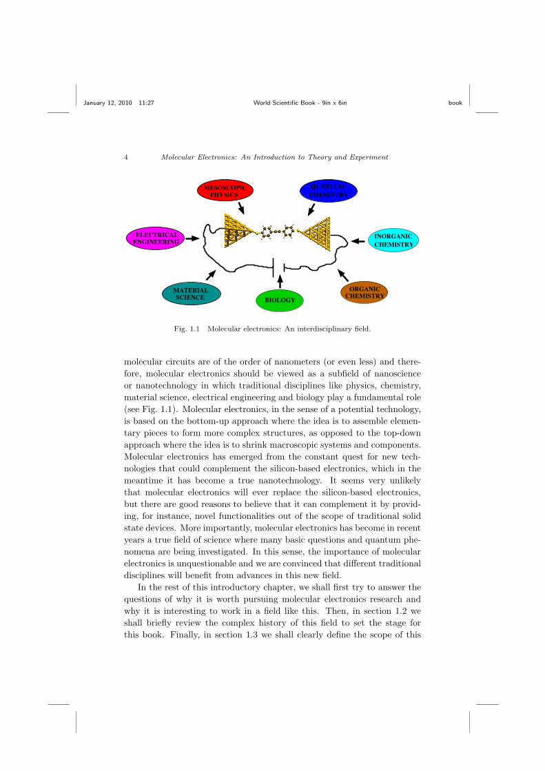
Molecular electronics, as used in this book, is defined as the field ofscience that investigates the electronic and thermal transport properties ofcircuits in which individual molecules (or an assembly of them) are used asbasic building blocks.1 Obviously, some of the feature dimensions of such
1Molecular electronics, in the sense used here, should not be confused with organicelectronics, the field in which molecular materials are investigated as possible constituentsof a variety of macroscopic electronic devices.
3
January 12, 2010 11:27 World Scientific Book - 9in x 6in book
4 Molecular Electronics: An Introduction to Theory and Experiment
MESOSCOPIC PHYSICS
MATERIALSCIENCE BIOLOGY
ORGANICCHEMISTRY
QUANTUMCHEMISTRY
INORGANICCHEMISTRY
ELECTRICALENGINEERING
Fig. 1.1 Molecular electronics: An interdisciplinary field.
molecular circuits are of the order of nanometers (or even less) and there-fore, molecular electronics should be viewed as a subfield of nanoscienceor nanotechnology in which traditional disciplines like physics, chemistry,material science, electrical engineering and biology play a fundamental role(see Fig. 1.1). Molecular electronics, in the sense of a potential technology,is based on the bottom-up approach where the idea is to assemble elemen-tary pieces to form more complex structures, as opposed to the top-downapproach where the idea is to shrink macroscopic systems and components.Molecular electronics has emerged from the constant quest for new tech-nologies that could complement the silicon-based electronics, which in themeantime it has become a true nanotechnology. It seems very unlikelythat molecular electronics will ever replace the silicon-based electronics,but there are good reasons to believe that it can complement it by provid-ing, for instance, novel functionalities out of the scope of traditional solidstate devices. More importantly, molecular electronics has become in recentyears a true field of science where many basic questions and quantum phe-nomena are being investigated. In this sense, the importance of molecularelectronics is unquestionable and we are convinced that di!erent traditionaldisciplines will benefit from advances in this new field.
In the rest of this introductory chapter, we shall first try to answer thequestions of why it is worth pursuing molecular electronics research andwhy it is interesting to work in a field like this. Then, in section 1.2 weshall briefly review the complex history of this field to set the stage forthis book. Finally, in section 1.3 we shall clearly define the scope of this
January 12, 2010 11:27 World Scientific Book - 9in x 6in book
The birth of molecular electronics 5
monograph and explain its structure.
1.1 Why molecular electronics?
Every researcher is sooner or later confronted with natural questions like“why do you work in your field?” or “what is your research good for?”Of course, the answers are always personal, but in the case of molecularelectronics they also depend on whether one’s interests are closer to fun-damental science or to technological applications. From the point of viewof basic science, molecular electronics o!ers, for instance, the possibility toinvestigate electronic and thermal conduction at the smallest imaginablescale, where the physics is completely dominated by quantum mechanicale!ects. The small feature dimensions of molecular circuits together with thegreat variety of electrical, mechanical and optical properties of moleculescan give rise to countless new physical phenomena. Molecular junctions arealso ideal systems where to investigate and shed new light into the funda-mental electron transfer mechanisms that play a key role both in chemistryand biology. These reasons and many others make molecular electronics avery attractive field of basic research. Moreover, we should never forget thatthe history of science proves that the exploration of new territories and thesubsequent discovery of novel phenomena often lead to unexpected tech-nological applications. History also teaches us that there is no technologywithout basic understanding and thus, the future of molecular electronicsas an emerging technology depends on our ability to understand the funda-mental mechanisms that govern the electronic conduction at the molecularscale.
From a technological point of view, there are also good reasons to inves-tigate the use of molecules as electronically active elements for a variety ofapplications. In comparison with the silicon-based technology, which is al-ready a nanotechnology in the sense that the structure sizes are in the rangeof nanometers,2 molecular electronics could in principle o!er the followingmajor advantages [2]:
• Size. The reduce size of small molecules (between 1 and 10 nm)could lead to a higher packing density of devices with the subse-quent advantages in cost, e"ciency, and power dissipation.
2The next generation of transistors for advanced microprocessors will have gate lengthsof 22 nm and a SiO2 gate oxide thickness of less than 1.2 nm [1].

January 12, 2010 11:27 World Scientific Book - 9in x 6in book
6 Molecular Electronics: An Introduction to Theory and Experiment
• Speed. Although most molecules are poorly conductive, goodmolecular wires could reduce the transit time of typical transis-tors (! 10!14 s), reducing so the time needed for an operation.
• Assembly and recognition. One can exploit specific intermolecularinteractions to form structures by nanoscale self-assembly. Molec-ular recognition can be used to modify electronic behavior, provid-ing both switching and sensing capabilities on the single-moleculescale.
• New functionalities. Special properties of molecules, like the exis-tence of distinct stable geometric structures or isomers, could leadto new electronic functions that are not possible to implement inconventional solid state devices.
• Synthetic tailorability. By choice of composition and geometry, onecan extensively vary a molecule’s transport, binding, optical, andstructural properties. The tools of molecular synthesis are highlydeveloped.
Molecules have also obvious disadvantages such as instabilities at hightemperatures. Moreover, the fabrication of reliable molecular junctionsrequires sometimes to control matter at an unprecedented level, which canbe not only di!cult, but also slow and costly. Anyway, the advantagesdescribed above are su!cient to motivate the exploration of a molecule-based electronics.
1.2 A brief history of molecular electronics
It is always di!cult to trace back the history of an emerging field and tosummarize it in a few pages. Anyway, even at the risk of being unfair leavingout some important contributors, we find necessary to say a few words aboutthe history of molecular electronics as a tribute to those visionary scientiststhat made possible that we are now working in this fascinating field. Ourbrief account here is partially based on a delightful (non-scientific) articleby Choi and Mody [3], which reviews the history of molecular electronicspaying special attention to its social aspects.
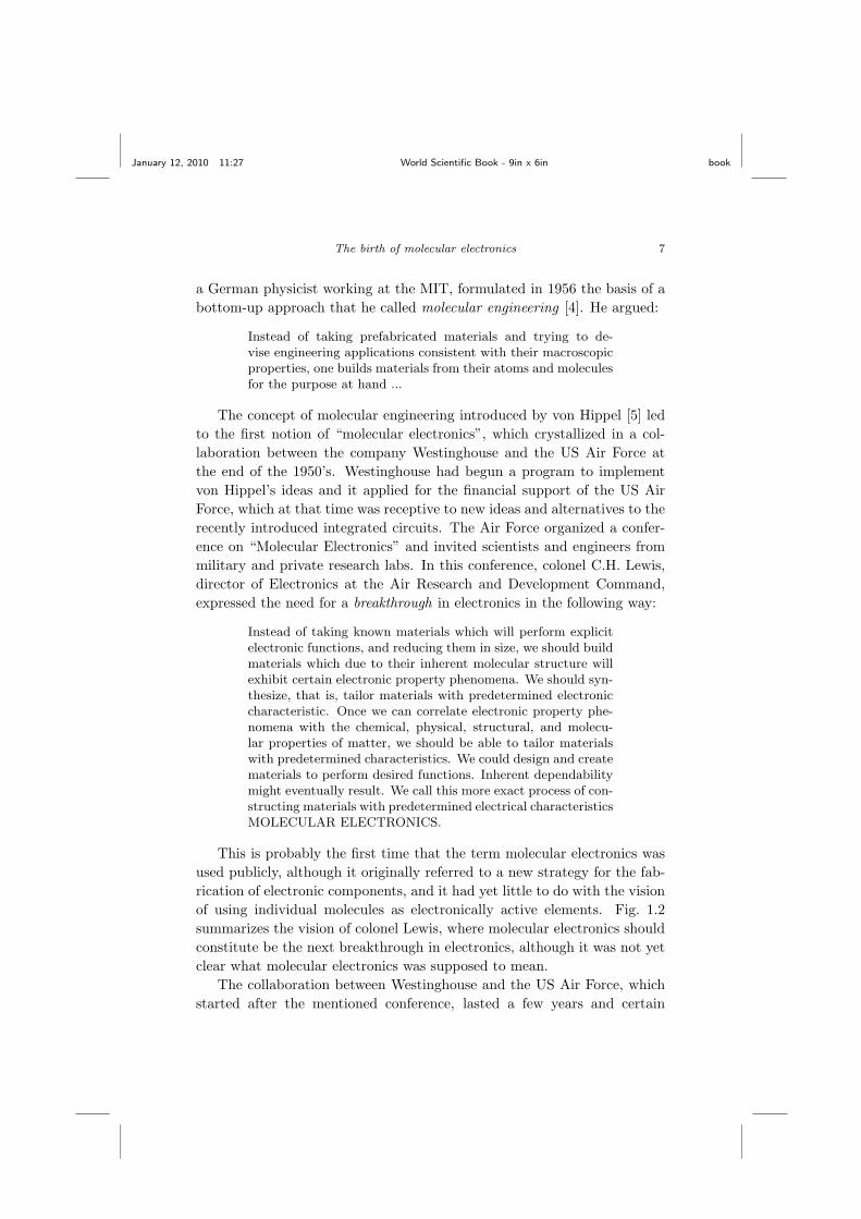
We start this historical review in 1950’s, after the revolution in electron-ics due to the invention of the transistor and the subsequent introductionof integrated circuits. In that context and in view of the di!culties to rad-ically miniaturize the existent electronic components, Arthur von Hippel,
January 12, 2010 11:27 World Scientific Book - 9in x 6in book
The birth of molecular electronics 7
a German physicist working at the MIT, formulated in 1956 the basis of abottom-up approach that he called molecular engineering [4]. He argued:
Instead of taking prefabricated materials and trying to de-vise engineering applications consistent with their macroscopicproperties, one builds materials from their atoms and moleculesfor the purpose at hand ...
The concept of molecular engineering introduced by von Hippel [5] ledto the first notion of “molecular electronics”, which crystallized in a col-laboration between the company Westinghouse and the US Air Force atthe end of the 1950’s. Westinghouse had begun a program to implementvon Hippel’s ideas and it applied for the financial support of the US AirForce, which at that time was receptive to new ideas and alternatives to therecently introduced integrated circuits. The Air Force organized a confer-ence on “Molecular Electronics” and invited scientists and engineers frommilitary and private research labs. In this conference, colonel C.H. Lewis,director of Electronics at the Air Research and Development Command,expressed the need for a breakthrough in electronics in the following way:
Instead of taking known materials which will perform explicitelectronic functions, and reducing them in size, we should buildmaterials which due to their inherent molecular structure willexhibit certain electronic property phenomena. We should syn-thesize, that is, tailor materials with predetermined electroniccharacteristic. Once we can correlate electronic property phe-nomena with the chemical, physical, structural, and molecu-lar properties of matter, we should be able to tailor materialswith predetermined characteristics. We could design and creatematerials to perform desired functions. Inherent dependabilitymight eventually result. We call this more exact process of con-structing materials with predetermined electrical characteristicsMOLECULAR ELECTRONICS.
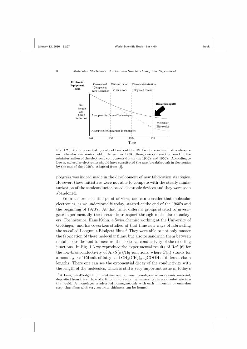
This is probably the first time that the term molecular electronics wasused publicly, although it originally referred to a new strategy for the fab-rication of electronic components, and it had yet little to do with the visionof using individual molecules as electronically active elements. Fig. 1.2summarizes the vision of colonel Lewis, where molecular electronics shouldconstitute be the next breakthrough in electronics, although it was not yetclear what molecular electronics was supposed to mean.
The collaboration between Westinghouse and the US Air Force, whichstarted after the mentioned conference, lasted a few years and certain
January 12, 2010 11:27 World Scientific Book - 9in x 6in book
8 Molecular Electronics: An Introduction to Theory and Experiment
Electronic
TrendEquipment Conventioal
ComponentSize Reduction (Integrated Circuit)(Transistor)
SizeWeight
and
Reduction
Breakthrough!!!
ElectronicsMolecular
1940
Asymptote for Present Technologies
Asymptote for Molecular Technologies
1950 1954 1958Time
Miniaturization Microminiaturization
Space
Fig. 1.2 Graph presented by colonel Lewis of the US Air Force in the first conferenceon molecular electronics held in November 1958. Here, one can see the trend in theminiaturization of the electronic components during the 1940’s and 1950’s. According toLewis, molecular electronics should have constituted the next breakthrough in electronicsby the end of the 1950’s. Adapted from [3].
progress was indeed made in the development of new fabrication strategies.However, these initiatives were not able to compete with the steady minia-turization of the semiconductor-based electronic devices and they were soonabandoned.
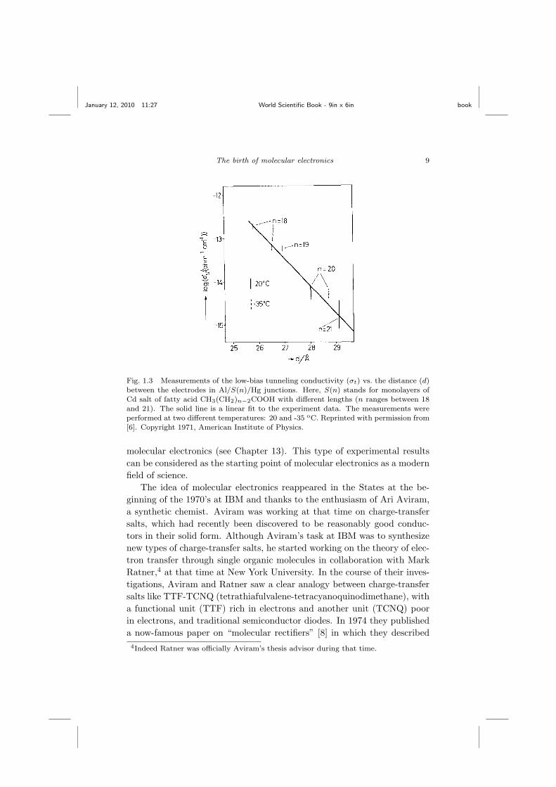
From a more scientific point of view, one can consider that molecularelectronics, as we understand it today, started at the end of the 1960’s andthe beginning of 1970’s. At that time, di!erent groups started to investi-gate experimentally the electronic transport through molecular monolay-ers. For instance, Hans Kuhn, a Swiss chemist working at the University ofGottingen, and his coworkers studied at that time new ways of fabricatingthe so-called Langmuir-Blodgett films.3 They were able to not only masterthe fabrication of these molecular films, but also to sandwich them betweenmetal electrodes and to measure the electrical conductivity of the resultingjunctions. In Fig. 1.3 we reproduce the experimental results of Ref. [6] forthe low-bias conductivity of Al/S(n)/Hg junctions, where S(n) stands fora monolayer of Cd salt of fatty acid CH3(CH2)n!2COOH of di!erent chainlengths. There one can see the exponential decay of the conductivity withthe length of the molecules, which is still a very important issue in today’s3A Langmuir-Blodgett film contains one or more monolayers of an organic material,
deposited from the surface of a liquid onto a solid by immersing the solid substrate intothe liquid. A monolayer is adsorbed homogeneously with each immersion or emersionstep, thus films with very accurate thickness can be formed.
January 12, 2010 11:27 World Scientific Book - 9in x 6in book
The birth of molecular electronics 9
Fig. 1.3 Measurements of the low-bias tunneling conductivity (!t) vs. the distance (d)between the electrodes in Al/S(n)/Hg junctions. Here, S(n) stands for monolayers ofCd salt of fatty acid CH3(CH2)n!2COOH with di!erent lengths (n ranges between 18and 21). The solid line is a linear fit to the experiment data. The measurements wereperformed at two di!erent temperatures: 20 and -35 oC. Reprinted with permission from[6]. Copyright 1971, American Institute of Physics.
molecular electronics (see Chapter 13). This type of experimental resultscan be considered as the starting point of molecular electronics as a modernfield of science.
The idea of molecular electronics reappeared in the States at the be-ginning of the 1970’s at IBM and thanks to the enthusiasm of Ari Aviram,a synthetic chemist. Aviram was working at that time on charge-transfersalts, which had recently been discovered to be reasonably good conduc-tors in their solid form. Although Aviram’s task at IBM was to synthesizenew types of charge-transfer salts, he started working on the theory of elec-tron transfer through single organic molecules in collaboration with MarkRatner,4 at that time at New York University. In the course of their inves-tigations, Aviram and Ratner saw a clear analogy between charge-transfersalts like TTF-TCNQ (tetrathiafulvalene-tetracyanoquinodimethane), witha functional unit (TTF) rich in electrons and another unit (TCNQ) poorin electrons, and traditional semiconductor diodes. In 1974 they publisheda now-famous paper on “molecular rectifiers” [8] in which they described
4Indeed Ratner was o"cially Aviram’s thesis advisor during that time.
January 12, 2010 11:27 World Scientific Book - 9in x 6in book
10 Molecular Electronics: An Introduction to Theory and Experiment
how a modified charge-transfer salt could operate as a traditional diodein an electrical circuit. This is probably the first proposal to use a sin-gle molecule as an electronic component, which is something that lies atthe heart of the modern molecular electronics. Aviram and Ratner’s ideawas considered during a long time a theoretical curiosity that could not betested experimentally and in this sense, it did not have much impact in thescientific community at that time.
In the late 1970’s and early 1980’s other scientists started to work onideas similar to Aviram-Ratner’s unimolecular concept. Let us mention forinstance the name of Forrest Carter, a chemist at the Naval Research Lab-oratory, who was certainly influenced by Feynman’s (1960) famous “Roomat the Bottom” speech [9]. Carter introduced concepts such as molecularcomputing or cellular automata, where the essence was to use individualmolecules as the ultimate electronic components or as elementary unitswhere to store bits of information in a hypothetical molecular computer.These ideas were to a large extend purely theoretical and they were no sup-ported by real experiments. However, Carter was able to nucleate a firstmolecular electronics community around him and, in particular, the orga-nization of a series of conferences on molecular electronics in the 1980’splayed an important role in the history of this field. People like RobertMetzger, Mark Reed and others, who played later an important role inmolecular electronics, attended those conferences and they were inspiredby the discussions held there.
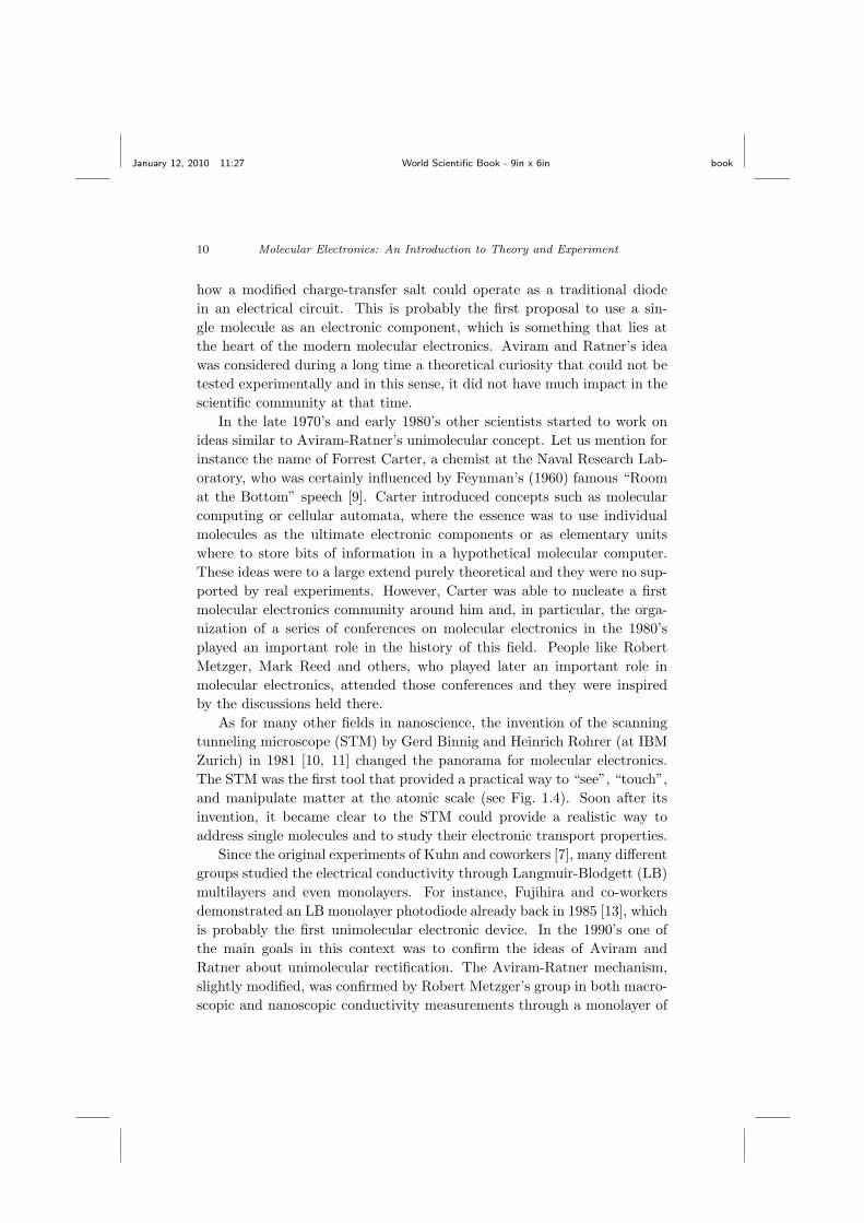
As for many other fields in nanoscience, the invention of the scanningtunneling microscope (STM) by Gerd Binnig and Heinrich Rohrer (at IBMZurich) in 1981 [10, 11] changed the panorama for molecular electronics.The STM was the first tool that provided a practical way to “see”, “touch”,and manipulate matter at the atomic scale (see Fig. 1.4). Soon after itsinvention, it became clear to the STM could provide a realistic way toaddress single molecules and to study their electronic transport properties.
Since the original experiments of Kuhn and coworkers [7], many di!erentgroups studied the electrical conductivity through Langmuir-Blodgett (LB)multilayers and even monolayers. For instance, Fujihira and co-workersdemonstrated an LB monolayer photodiode already back in 1985 [13], whichis probably the first unimolecular electronic device. In the 1990’s one ofthe main goals in this context was to confirm the ideas of Aviram andRatner about unimolecular rectification. The Aviram-Ratner mechanism,slightly modified, was confirmed by Robert Metzger’s group in both macro-scopic and nanoscopic conductivity measurements through a monolayer of
January 12, 2010 11:27 World Scientific Book - 9in x 6in book
The birth of molecular electronics 11
Fig. 1.4 Principle of a local probe like the scanning tunneling microscope: The gentletouch of a nanofinger. If the interaction between tip and sample decays su!cientlyrapidly on the atomic scale, only the two atoms that are closest to each other are able to“feel” each other. Reprinted with permission from [12]. Copyright 1999 by the AmericanPhysical Society.
!-hexadecyl-quinolinium tricyanoquinomethanide in 1997 [14].At the end of the 1980’s and the beginning of the 1990’s the appear-
ance of the metallic atomic-sized contacts had an important impact in thenanoscience community. Di!erent groups showed that the STM and therecently introduced mechanically controllable break junction (MCBJ) tech-nique5 could be used to fabricate metallic wires of atomic dimensions (for areview, see Ref. [15]). Since then these nanowires have become an endlesssource of new physical phenomena and have played a crucial role in the fieldsof mesoscopic physics and nanoelectronics. The relevance of these systemsfor molecular electronics is two-fold. On the one hand, they provide thebasis to contact individual molecules with dimensions on the range of a fewnanometers, which is out of the scope of conventional lithographies. Onthe other hand, the atomic contacts have allowed establishing the connec-tion between the quantum properties of single atoms and the macroscopicelectrical properties of the circuits in which they are embedded, which isan important lesson for molecular electronics.6
In 1997 the collaboration between the groups of Mark Reed (a physicistat Yale University) and James Tour (a synthetic chemist at the Universityof South Carolina) led to the publication of the results of what is oftenconsidered as the first transport experiment in single-molecule junctions[16].7 These authors used the MCBJ technique to contact benzenedithiol
5This technique will be described in the next chapter.6The physics of these metallic nanowires will be described in the third part of this
monograph.7Let us clarify that the first transport measurements involving single molecules were
indeed performed with the STM, but the experiment of Reed et al. is the first one realized
January 12, 2010 11:27 World Scientific Book - 9in x 6in book
12 Molecular Electronics: An Introduction to Theory and Experiment
Solvent evaporates, then tipsbrought together until theonset of conductance
Add THF and benzene−1,4−dithiol
(a)
(b)
Gold wire
Gold wire
Wire stretched until breakage,resulting in tip formation
SAM
SAM
Goldelectrode
Goldelectrode
(c)
electrodeGold Gold
electrode
(d)
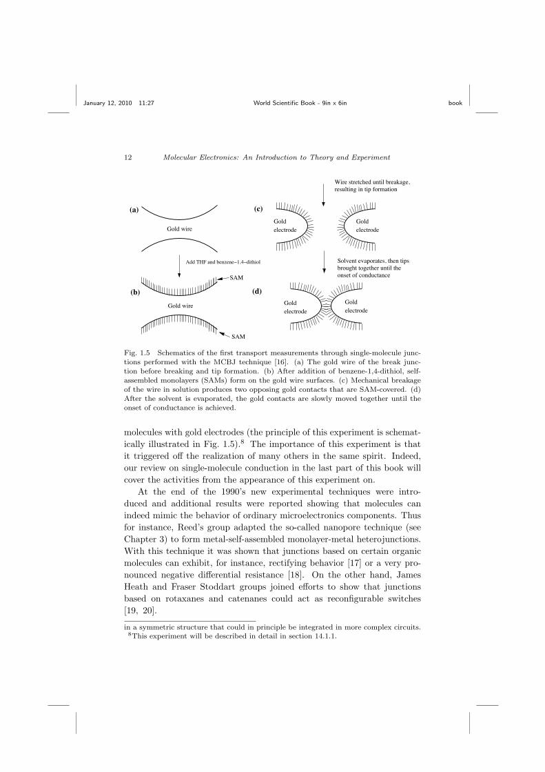
Fig. 1.5 Schematics of the first transport measurements through single-molecule junc-tions performed with the MCBJ technique [16]. (a) The gold wire of the break junc-tion before breaking and tip formation. (b) After addition of benzene-1,4-dithiol, self-assembled monolayers (SAMs) form on the gold wire surfaces. (c) Mechanical breakageof the wire in solution produces two opposing gold contacts that are SAM-covered. (d)After the solvent is evaporated, the gold contacts are slowly moved together until theonset of conductance is achieved.
molecules with gold electrodes (the principle of this experiment is schemat-ically illustrated in Fig. 1.5).8 The importance of this experiment is thatit triggered o! the realization of many others in the same spirit. Indeed,our review on single-molecule conduction in the last part of this book willcover the activities from the appearance of this experiment on.
At the end of the 1990’s new experimental techniques were intro-duced and additional results were reported showing that molecules canindeed mimic the behavior of ordinary microelectronics components. Thusfor instance, Reed’s group adapted the so-called nanopore technique (seeChapter 3) to form metal-self-assembled monolayer-metal heterojunctions.With this technique it was shown that junctions based on certain organicmolecules can exhibit, for instance, rectifying behavior [17] or a very pro-nounced negative di!erential resistance [18]. On the other hand, JamesHeath and Fraser Stoddart groups joined e!orts to show that junctionsbased on rotaxanes and catenanes could act as reconfigurable switches[19, 20].
in a symmetric structure that could in principle be integrated in more complex circuits.8This experiment will be described in detail in section 14.1.1.
January 12, 2010 11:27 World Scientific Book - 9in x 6in book
The birth of molecular electronics 13
Techniques like electromigration [21], which were specially designed tocontact single molecules, were developed at the turn of the century. Thesemethods made possible to incorporate a gate electrode in single-moleculejunctions and thus, to mimic the measurements performed in solid statedevices like transistors or in nanostructures like quantum dots. With the useof these techniques it was possible to show that single-molecule junctionscan behave as a new kind of single-electron transistors [22] or that theycan exhibit basic physical phenomena like Coulomb blockade or the Kondoe!ect [23, 24], which are well-known in the context of other nanoscopicstructures.
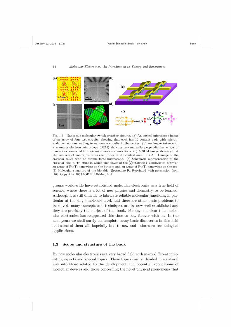
These results obtained in academic institutions and research laborato-ries attracted the attention of global players in information technology likeHP, IBM and others that decided to set up small molecular electronicsresearch groups. This gave a new impulse to the field by providing veryimportant missing ingredients like, for instance, strategies to link moleculardevices with each other and with external systems. As an example we canmention the nanoscale circuits based on a configurable crossbar architec-ture introduced by Stanley Williams and coworkers at the HP Laboratoriesin Palo Alto [25], see Fig. 1.6(a-d). This strategy was used, for instance,to show that molecular crossbar circuits fabricated from a molecular mono-layer of [2]rotaxanes can function as an ultra-high-density memory [26],see Fig. 1.6(e-f). The working principle of these molecular memories issupposed to be based on the ability of molecules like rotaxanes to switchbetween two metastable states upon the application of an external biasvoltage. The actual origin of the switching behavior in these molecularjunctions has been heavily debated and, in some cases, it has shown thatthe metal electrodes or the metal-molecule interface are responsible forthe switching mechanism rather than the molecules themselves (see e.g.Ref. [27]). The controversy about these results, and also about some ofthe original experiments mentioned above, led to the extended belief thatmolecular electronics was going through a midlife crisis [28], although it wasno more than a teenager. In the meantime, the situation concerning themolecular memories has been clarified to a large extend and more recentlythe densest memory circuit ever made (1011 bits cm!2) was fabricated usinga monolayer of bistable [2]rotaxane molecules as the data storage elements[29]. Although many scientific and engineering challenges, such as devicerobustness, remain to be addressed before these devices can be practical,these results show clearly the potential of a molecule-based electronics.
On the other hand, the e!orts in recent years of numerous research
January 12, 2010 11:27 World Scientific Book - 9in x 6in book
14 Molecular Electronics: An Introduction to Theory and Experiment
(a)
(d)(c)
(f)
(e)
(b)
Fig. 1.6 Nanoscale molecular-switch crossbar circuits. (a) An optical microscope imageof an array of four test circuits, showing that each has 16 contact pads with micron-scale connections leading to nanoscale circuits in the center. (b) An image taken witha scanning electron microscope (SEM) showing two mutually perpendicular arrays ofnanowires connected to their micron-scale connections. (c) A SEM image showing thatthe two sets of nanowires cross each other in the central area. (d) A 3D image of thecrossbar taken with an atomic force microscope. (e) Schematic representation of thecrossbar circuit structure in which monolayer of the [2]rotaxane is sandwiched betweenan array of Pt/Ti nanowires on the bottom and an array of Pt/Ti nanowires on the top.(f) Molecular structure of the bistable [2]rotaxane R. Reprinted with permission from[26]. Copyright 2003 IOP Publishing Ltd.
groups world-wide have established molecular electronics as a true field ofscience, where there is a lot of new physics and chemistry to be learned.Although it is still di!cult to fabricate reliable molecular junctions, in par-ticular at the single-molecule level, and there are other basic problems tobe solved, many concepts and techniques are by now well established andthey are precisely the subject of this book. For us, it is clear that molec-ular electronics has reappeared this time to stay forever with us. In thenext years we shall surely contemplate many basic discoveries in this fieldand some of them will hopefully lead to new and unforeseen technologicalapplications.
1.3 Scope and structure of the book
By now molecular electronics is a very broad field with many di"erent inter-esting aspects and special topics. These topics can be divided in a naturalway into those related to the development and potential applications ofmolecular devices and those concerning the novel physical phenomena that
January 12, 2010 11:27 World Scientific Book - 9in x 6in book
The birth of molecular electronics 15
take place in molecular-scale junctions. In this monograph we are interestedin the latter type of topics and, in particular, we shall focus our attentionon the understanding of the basic mechanisms that dominate the electronictransport at the molecular scale. To be precise, we shall concentrate onthe analysis of the properties of single-molecule junctions, although someexamples of junctions based on molecular assemblies will also be presentedand discussed.
Our main goal in this monograph is two-fold. On the one hand, we wantto provide a true textbook on molecular electronic for advanced undergrad-uate and graduate students both in physics and chemistry. The book hasbeen designed so that, by the end of it, a student with a background inquantum mechanics and some elementary notions of solid state physics9
and organic chemistry10 should be able to start doing research in the fieldof molecular electronics. On the other hand, we also want to provide athorough review of the activities on single-molecule conduction over thelast ten years, from which both newcomers and researches working in thefield can profit.
With this double goal in mind, we have divided this monograph intofour parts that can be read independently.11 The first two are meant astextbook material that can be used for a regular course, while the last twoones are closer to a topical review. Part 1 includes, apart from this intro-ductory chapter, a detailed description of the experimental techniques thatare currently being used to fabricate both atomic-scale wires and molecularjunctions as well as the basic principles of transport measurements. Here,we have tried to explain both the basis of the di!erent techniques as well astheir advantages and disadvantages. Moreover, we have included in section3.2 a brief discussion about the main molecules used in molecular electron-ics and their basic properties, which can be viewed as an accelerated coursein organic chemistry.
Part 2 contains an extensive theoretical background that provides a ba-sic introduction both to the transport mechanisms in nanoscale systemsand to the standard theoretical techniques that are used to describe thetransport in molecular systems. We want to stress that this theory part isnot just meant for theoreticians and theory-inclined students, but for every-
9For the students in chemistry we recommend the brief introduction to solid statephysics provided in chapter 4 of Ref. [30] or in chapter 3 of Ref. [31].10For the students in physics we recommend the brief introduction to organic chemistryprovided in chapter 5 of Ref. [31].11There is indeed a fifth part that contains an appendix about the second quantizationformalism of quantum mechanics.
January 12, 2010 11:27 World Scientific Book - 9in x 6in book
16 Molecular Electronics: An Introduction to Theory and Experiment
body. All the topics are discussed in a didactic and self-contained mannerso that students without a previous knowledge on these topics should beable, after reading this part, to follow the theory papers in this field. Tobe precise, this part starts in Chapter 4 with an introduction to the scat-tering (or Landauer) approach, which provides an appealing framework todescribe coherent transport in nanostructures. Then, we go on with severalchapters devoted to Green’s function techniques (Chapters 5-8), which pro-vide powerful tools to compute equilibrium and nonequilibrium propertiesof atomic-scale junctions beyond the capabilities of the scattering approach.Finally, Chapters 9 and 10 deal with the two most widely used electronicstructure methods in molecular electronics, namely the tight-binding ap-proach and density functional theory. These methods in combination withthe Green’s function techniques provide the starting point for the realisticdescription of the transport properties of atomic and molecular junctions.Let us emphasize that at the end of every chapter one can find severalexercises that have been chosen to illustrate the main concepts.
Part 3 presents a basic description of the physics of atomic-sized con-tacts. Although this is not the main topic of the book, it is crucial tohave a basic knowledge about the transport properties of the metallic wiresthat are then used as electrodes in molecular junctions. We have dividedthis part into two chapters where we describe the physics of non-magneticatomic contacts (Chapter 11) and magnetic ones (Chapter 12).
Finally, Part 4 presents a detailed review on the transport throughmolecular junctions. We have organized the material according to the phys-ical mechanism which dominates the transport properties. Thus, we startthis part with two chapters devoted to the coherent transport in molecularjunctions (Chapters 13 and 14). Then, we discuss in Chapter 15 the physicsof the so-called molecular transistors, which are nothing but weakly coupledmolecular junctions where the transport is dominated by electronic corre-lations that lead to phenomena like Coulomb blockade or the Kondo e!ect.We then proceed to discuss in Chapters 16 and 17 the role of molecularvibrations in the electrical current through molecular junctions. Chapter19 is devoted to other transport properties beyond conductance and wediscuss there, in particular, shot noise and thermal transport in molecularconductors. The optical properties of current-currying molecular junctionsare the subject of Chapter 20. Chapter 18 deals with the electronic trans-port in long molecules where the hopping (or incoherent) transport regimeis realized. Finally, we conclude this part in Chapter 21 with a list of topicsthat have not been addressed in this monograph and we indicate where to
January 12, 2010 11:27 World Scientific Book - 9in x 6in book
The birth of molecular electronics 17
find information about them. It is worth remarking that these chaptershave been written so that they can be read almost independently. Thisway a reader can concentrate on those topics or chapters that are of specialinterest for him/her.
Parts 3 and 4 are meant for both students and researchers working inthe field. We do not only review what has recently been done in the field,but we also introduce the di!erent topics at a elementary level. In thissense, whenever it was possible, we have provided simple arguments andsuggested additional exercises. These two parts are intended for both exper-imentalists and theoreticians and, most of the time, we have intentionallyavoided the typical separation between experiment and theory, which wefind particularly harmful in this field.
Let us close this chapter with some recommendations about the existentliterature. For those who want a quick overview about molecular electron-ics, we recommend the short reviews of Refs. [2, 32–37]. A nice generaloverview of the field can be found in chapter 20 of Ref. [31]. For more ex-tensive introductions, we recommend Ref. [38] for the theory in molecularsystems and Refs. [39–41] for a discussion of the experimental techniquesused in molecular electronics. There already exist several books that dealwith di!erent aspects of molecular electronics, see e.g. Refs. [42–49]. Mostof them consist of a collection of articles written by di!erent authors, butthey are very useful if one wants a more detailed discussion of certain topics.Concerning the theory of quantum transport or transport in nanoscale sys-tems, which is one of the central subjects of this manuscript, we recommendthe monographs of Refs. [50–53].