
Molecular dewetting on insulators - McGill Physicspeter/publications/dewettingreview.pdf ·...
16
IOP PUBLISHING JOURNAL OF PHYSICS: CONDENSED MATTER J. Phys.: Condens. Matter 21 (2009) 423101 (16pp) doi:10.1088/0953-8984/21/42/423101 TOPICAL REVIEW Molecular dewetting on insulators S A Burke 1 , J M Topple 2 and P Gr ¨ utter 2 1 Department of Physics, University of California Berkeley, Berkeley, CA, USA 2 Department of Physics, McGill University, Montreal, QC, Canada E-mail: [email protected] Received 1 July 2009, in final form 4 August 2009 Published 8 September 2009 Online at stacks.iop.org/JPhysCM/21/423101 Abstract Recent attention given to the growth and morphology of organic thin films with regard to organic electronics has led to the observation of dewetting (a transition from layer(s) to islands) of molecular deposits in many of these systems. Dewetting is a much studied phenomenon in the formation of polymer and liquid films, but its observation in thin films of the ‘small’ molecules typical of organic electronics requires additional consideration of the structure of the interface between the molecular film and the substrate. This review covers some key concepts related to dewetting and molecular film growth. In particular, the origins of different growth modes and the thickness dependent interactions which give rise to dewetting are discussed in terms of surface energies and the disjoining pressure. Characteristics of molecular systems which may lead to these conditions, including the formation of metastable interface structures and commensurate–incommensurate phase transitions, are also discussed. Brief descriptions of some experimental techniques which have been used to study molecular dewetting are given as well. Examples of molecule-on-insulator systems which undergo dewetting are described in some detail, specifically perylene derivatives on alkali halides, C 60 on alkali halides, and the technologically important system of pentacene on SiO 2 . These examples point to some possible predicting factors for the occurrence of dewetting, most importantly the formation of an interface layer which differs from the bulk crystal structure. (Some figures in this article are in colour only in the electronic version) Contents 1. Introduction 1 2. Surface energies, growth modes and dewetting 2 3. Experimental methods for studying dewetting 5 4. Examples of molecule-on-insulator growth exhibiting dewetting 6 4.1. Perylene derivatives on alkali halides: epitaxy driven dewetting 6 4.2. C 60 on alkali halides: a morphological effect of dewetting 10 4.3. Pentacene on SiO 2 : dewetting in a technologi- cally important system 11 4.4. Overview of example systems 13 5. Summary 13 Acknowledgments 14 References 14 1. Introduction The production, characterization and growth of organic materials has received substantial attention in recent years, particularly with an eye towards use as functional components in devices [1, 2]. The potential for mass production of complex nanoscale objects with a wide range of engineered functionality through chemical means makes the use of organic materials extremely attractive. Indeed, the use of organic thin films in electronic and optoelectronic device applications has seen a great deal of progress to date with products already to market, and the promise of novel, inexpensive low energy processed devices ranging from flexible displays to low-cost, light-weight solar panels lingering on the horizon [3]. However, molecular materials are often sensitive to their local environment, and as such, the microscopic interfaces in any functional organic composite or device must be carefully understood and controlled. Despite the progress that has been 0953-8984/09/423101+16$30.00 © 2009 IOP Publishing Ltd Printed in the UK 1
-
Upload
truongcong -
Category
Documents
-
view
213 -
download
0
Transcript of Molecular dewetting on insulators - McGill Physicspeter/publications/dewettingreview.pdf ·...
IOP PUBLISHING JOURNAL OF PHYSICS: CONDENSED MATTER
J. Phys.: Condens. Matter 21 (2009) 423101 (16pp) doi:10.1088/0953-8984/21/42/423101
TOPICAL REVIEW
Molecular dewetting on insulatorsS A Burke1, J M Topple2 and P Grutter2
1 Department of Physics, University of California Berkeley, Berkeley, CA, USA2 Department of Physics, McGill University, Montreal, QC, Canada
E-mail: [email protected]
Received 1 July 2009, in final form 4 August 2009Published 8 September 2009Online at stacks.iop.org/JPhysCM/21/423101
AbstractRecent attention given to the growth and morphology of organic thin films with regard toorganic electronics has led to the observation of dewetting (a transition from layer(s) to islands)of molecular deposits in many of these systems. Dewetting is a much studied phenomenon inthe formation of polymer and liquid films, but its observation in thin films of the ‘small’molecules typical of organic electronics requires additional consideration of the structure of theinterface between the molecular film and the substrate. This review covers some key conceptsrelated to dewetting and molecular film growth. In particular, the origins of different growthmodes and the thickness dependent interactions which give rise to dewetting are discussed interms of surface energies and the disjoining pressure. Characteristics of molecular systemswhich may lead to these conditions, including the formation of metastable interface structuresand commensurate–incommensurate phase transitions, are also discussed. Brief descriptions ofsome experimental techniques which have been used to study molecular dewetting are given aswell. Examples of molecule-on-insulator systems which undergo dewetting are described insome detail, specifically perylene derivatives on alkali halides, C60 on alkali halides, and thetechnologically important system of pentacene on SiO2. These examples point to some possiblepredicting factors for the occurrence of dewetting, most importantly the formation of aninterface layer which differs from the bulk crystal structure.
(Some figures in this article are in colour only in the electronic version)
Contents
1. Introduction 12. Surface energies, growth modes and dewetting 23. Experimental methods for studying dewetting 54. Examples of molecule-on-insulator growth exhibiting
dewetting 64.1. Perylene derivatives on alkali halides: epitaxy
driven dewetting 64.2. C60 on alkali halides: a morphological effect
of dewetting 104.3. Pentacene on SiO2: dewetting in a technologi-
cally important system 114.4. Overview of example systems 13
5. Summary 13Acknowledgments 14References 14
1. Introduction
The production, characterization and growth of organicmaterials has received substantial attention in recent years,particularly with an eye towards use as functional componentsin devices [1, 2]. The potential for mass production ofcomplex nanoscale objects with a wide range of engineeredfunctionality through chemical means makes the use of organicmaterials extremely attractive. Indeed, the use of organicthin films in electronic and optoelectronic device applicationshas seen a great deal of progress to date with productsalready to market, and the promise of novel, inexpensive lowenergy processed devices ranging from flexible displays tolow-cost, light-weight solar panels lingering on the horizon [3].However, molecular materials are often sensitive to their localenvironment, and as such, the microscopic interfaces in anyfunctional organic composite or device must be carefullyunderstood and controlled. Despite the progress that has been
0953-8984/09/423101+16$30.00 © 2009 IOP Publishing Ltd Printed in the UK1

J. Phys.: Condens. Matter 21 (2009) 423101 Topical Review
made in developing thin film organic materials for electronicapplications, there remain fundamental questions regarding theinfluence of the device environment (i.e. electrodes, dielectric,encapsulation, and ambient conditions) on the properties oforganic semiconductors. For example, while it is knownthat the molecule–dielectric interface and arrangement ofmolecules within the first few layers is critical to organic thinfilm transistor device performance [4–7], these systems havebeen particularly difficult to explore on the molecular/atomicscale due to a lack of suitable tools and complications inapplying many well-established surface science techniques toboth molecules and insulators.
One of the first steps in optimizing organic thin filmdevices then is to better understand molecular epitaxy andgrowth on substrates of interest. This includes metallicsubstrates which define the molecule–electrode interface, aswell as insulating substrates which constitute the molecule–dielectic interface. There has been significant effort in studyingorganic film growth on a variety of substrates in recent yearsfor this reason [1, 8, 9, 2]. In the study of the growth ofthin and ultrathin organic films, the process of dewetting,whereby a film is broken up into crystallites or islands, hasbeen observed on a number of substrates. Some exampleswhere molecular dewetting has been observed include:pentacene on gold [10–12], 3,4,9,10-perylene tetracarboxylicdianhydride (PTCDA) on Ag(111) [13], perylene on Cu(110)and Au(111) [14], hexaazatriphenylene-hexacarbonitrile onAu [15], pentacene on SiO2 [12, 16], phenylthiophenefulgide on quartz [17], m-bis(4-n-octyloxystyryl)-benzeneon mica [18], diindenoperylene (DIP) on SiO2 [19, 20],C60 on KBr and NaCl [21], PTCDA on NaCl [22]and KCl [23], 3,4,9,10-perylene tetracarboxylic diimide(PTCDI) on NaCl [24], and N ,N ′ -dimethylperylene-2,4,9,10-bis(dicarboximide) (DiMe-PTCDI) on NaCl [25]. Dewettingrelates to the issue of stability of films, and much like otherroughening transitions, for organic thin film devices thesechanges in the large scale structure of the film, giving riseto holes and grain boundaries, may influence electronic andoptoelectronic properties. Additionally, dewetting is oftenaccompanied by a rearrangement of the interface layer andthese differences in structure may alter the properties of thefilm near critical interfaces [26].
For device design and characterization, it is importantto understand not just the structure and the resulting device-related properties, but also the long-term and thermalstability of the grown film. Organic films which undergostructural transition via annealing may then have limited rangeof acceptable processing temperatures and even operatingtemperatures. Similarly, if dewetting of an organic filmoccurs over a very long timescale, the device propertiesmay change over time, likely a very undesirable effect. Anunderstanding of both the structures formed during growthand the equilibrium morphologies and crystal structures areimportant to the successful development of technologies basedon organic thin films.
This review will cover aspects of organic film growthand dewetting, in particular focusing on possible predictingfactors for dewetting of organic thin films. From the list
Figure 1. Schematic illustration of growth modes. The deposit (A)and substrate (B) each have surface energies γA and γB respectively,as well as an energy arising from the interface between the two, γ ∗.The balance of these energies gives rise to different growth modes:island, Stranski–Krastanov, and layer-by-layer (middle, left to right).Another possibility is that the system forms closed layers which arenot stable and a transition can occur resulting in islands formed fromthese initial layers, which is known as dewetting.
above, one can note that organic thin films on insulatingsubstrates appear particularly susceptible to undergoingdewetting processes. Since dewetting appears to be particularlyprevalent for molecules on insulators, which are integral todevice applications such as OTFTs, the specific conditions ofthese systems which may lead to dewetting will be addressed.Several examples of organic thin films on insulating substratesare discussed in some detail, specifically perylene derivativeson alkali halides, C60 on alkali halides, and the technologicallyimportant system of pentacene on SiO2, in order to illustratesome of the features of dewetting systems and to highlightwhere further understanding is needed. While the focus of thisarticle will be primarily on insulating substrates, the featuresand origins of dewetting are expected to be shared by organicfilms on other substrates where this process occurs.
2. Surface energies, growth modes and dewetting
There are many treatments of the relation of surface energies togrowth modes in the literature [27–30], however, the followingwill review some key concepts which are related to dewetting.The equilibrium growth of macroscopic films is dictated by thebalance of surface energies of the substrate, γB, the deposit, γA
and the energy of the interface, γ ∗ formed between the two(see figure 1), all of which are related to the change in Gibbsfree energy required to create the surface or interface [27]. Ifthe energies of the deposit surface and the interface are greaterthan the surface energy of the substrate, γA + γ ∗ > γB, theinterface and surface area of the deposit will be minimized andislands or crystallites will be formed in the so-called Volmer–Webber or island growth mode. While under real growthconditions these may eventually grow into a continuous film
2

J. Phys.: Condens. Matter 21 (2009) 423101 Topical Review
as the space between islands is filled in, the film will showevidence of these origins in the form of grain boundaries andincreased roughness. If instead, the balance of energies favoursincreasing the area of the deposit (and the interface) overleaving an exposed substrate surface, γA + γ ∗ < γB, the filmgrowth will proceed in a layer-by-layer fashion, also knownas the Frank–van der Merwe growth mode. This will typicallyresult in smooth films so long as diffusion is sufficient to permitcompletion of one layer before the nucleation of subsequentlayers occurs. A third equilibrium growth mode occurs whenthe interface energy depends on thickness, for example whenstrain at the interface is gradually released in subsequentlayers, resulting in a combination of layer growth followedby islands which nucleate on top of the initial ‘wetting’ layer.This layer-plus-island, or Stranski–Krastanov, growth modeis sometimes exploited in the fabrication of self-assemblednanoscale structures (for example, self-assembled quantum dotstructures formed from semiconductor heterostructures). Theprediction of growth mode in this way by the balance of surfaceenergies is valid for the equilibrium case, however, growthis often not an equilibrium processes and kinetic parameterssuch as temperature, deposition rate and energy of the incidentparticles can also play a significant or even dominant role indetermining growth morphologies.
In vacuum deposited films the ‘dewetting’ scenario ariseswhen an initial film is formed during the non-equilibriumgrowth phase but is not the favoured morphology of thedeposited film, or, when one form is favoured for a very thinfilm but cannot support the growth of a thicker film. Dewettingis a film evolution process by which islands or crystallites areformed through the removal of a pre-existing wetting layer.This is in contrast to the Stranski–Krastanov growth modewhereby the wetting layer remains and is typically stable,i.e. the islands formed do not grow through the removalof the wetting layer. The process of dewetting is wellknown with respect to the evolution of liquid and polymerfilms [31–35] and the evolution for crystalline films followsa similar progression: the film is broken up through theformation of holes and/or droplets leading to the final non-wetting state [36]. As this evolution takes place through a masstransport process from the wetting layer into 3D crystallites orislands, dewetting can be categorized as a form of coarseningor ripening. As in Ostwald ripening, where large dropletsare more stable and grow at the expense of small droplets,dewetting proceeds as a competitive process whereby morestable features grow at the expense of a less stable population.If the wetting layer is sufficiently stable, or if diffusion barriersare high and effectively trap the wetting layer, annealing maybe necessary to initiate and/or accelerate the process.
The conditions for dewetting are similar in terms ofsurface energy to Stranski–Krastanov growth: the free energy,F , must have a dependence on the thickness of the film,e. This typically occurs for thin films when the thicknessof the film becomes of order the range of the interaction ofthe deposited layer with the substrate. This can arise as aresult of van der Waals interactions, electrostatic interactions,or other long range interactions, which can include thoserelated to structuring of the liquid, polymer or crystalline
deposit [30, 29, 37]. These interactions give rise to a correctionterm, P(e) in the free energy of the deposited film which isthickness dependent:
dF (e)
dA= γ ∗ + γA + P(e) (1)
or in terms of the surface tension of the film:
γA,film = γ ∗ + γA + P(e) + e�(e) (2)
where we have defined what is known as the ‘disjoiningpressure’ as � = ∂ P/∂e [30]. Note that often the disjoiningpressure is stated as � = ∂ F/∂e, which is equivalent sincethe surface energies of the two solids are independent of thethickness (this is encapsulated in the correction term P(e)).
The stability of wetting films are often characterized interms of the disjoining pressure which represents the differencebetween intermolecular interactions within the bulk and thosewithin an adsorbed film interacting with the substrate. If thefilm is unstable (P ′′(e) < 0), the film will undergo spontaneousdewetting and fluctuations in temperature and density can beamplified in the so-called ‘spinodal’ regime [38], potentiallygiving rise to interesting morphological features. If the filmis instead metastable (P ′′(e) > 0), the film dewets throughthe nucleation and expansion of denuded zones [30]. Thedependence of the disjoining pressure on film thickness canbe complex depending on the types and ranges of interactionsinvolved and whether structuring of the film near the surfacecontributes an additional significant term and/or results in theexistence of multiple isotherms [37]. This might includethe presence of different structures in a thin and a thickfilm. Measurement of the disjoining pressure as a functionof thickness has also been used to describe the evolution ofthe film morphology from film growth through nucleationof droplets, holes and finally holes induced by substratedefects [33].
The form of this correction term, and therefore thedisjoining pressure, depends on the specific interactionsinvolved in the system to be considered. For example,when van der Waals interactions dominate, which is the mostcommonly considered case, this term can be written as:
P(e) = A
12πe2(3)
where A is the Hamaker constant. However, for ultrathinfilms, where the thickness approaches the atomic or moleculardimensions of the deposit, modelling of the specific system tobe described is required as the structure of the film and theinterplay of different interactions play a significant role [30].
Nevertheless, the concept of disjoining pressure mayalso be useful in the description of dewetting of crystallinemolecular films. Here, the disjoining pressure arisesfrom the competition between intermolecular and adsorption(molecule–substrate) forces, much as in the case of liquidand polymer films. The crystalline structure can give riseto interface structures that differ significantly from the bulkstructure either due to an imposed commensurability fromthe substrate [22], or an adsorption geometry which differs
3

J. Phys.: Condens. Matter 21 (2009) 423101 Topical Review
from the bulk structure, for example a different tilt angle ofmolecules at the surface [6]. These interface structures maybe incompatible with the bulk structure leading to strain, or inmore extreme cases a forced rearrangement of the interface,giving rise to thickness dependent interactions.
For illustration purposes, we can consider a simplified 1Dcase of an imposed commensurability with the substrate lattice.No problem arises in the case where the deposited molecularlattice and the substrate lattice match, or nearly match, in bothlattice constant and geometry (see figure 2(a)). However thisis often not the case for molecules deposited on inorganiccrystalline substrates [39]. If the intermolecular binding energyis of the same order as the adsorption energy, but the latticesare mismatched, the situation where there are two nearly equalenergy adsorption sites can occur (see figure 2(b)): one whichis commensurate with the substrate lattice (metastable) and onewhich is close to the bulk lattice constant of the molecularmaterial (stable). Depending on the precise energy balanceand the size of the barrier formed between the two states incomparison to the thermal energy, a metastable commensuratephase may form and even be stable at a given temperature.The formation of these different possible epitaxies as a resultof lattice geometry and competing interactions can set up theconditions for dewetting. In the metastable commensuratestate the molecule–substrate interaction dominates and weexpect wetting of this phase, but not necessarily of thebulk-like phase where intermolecular interactions dominate.In terms of the free energy and the disjoining pressure,this amounts to different paths, or isotherms, of the freeenergy with respect to thickness of the film due to eachdistinct structure. In these cases the dewetting transitionis also accompanied by a change of the interface structurefrom commensurate to incommensurate. This accompanyingcommensurate–incommensurate transition may further assistthe dewetting process by providing dislocations [40] for holeformation to begin. While this is a simplified model to illustratethe possibility of a metastable state which could give riseto dewetting, real molecular systems have additional factorswhich should be considered, including additional degreesof freedom such as rotation and conformation, anisotropicinteractions between molecules and between the moleculeand substrate, and relatively soft interactions allowing forgreater strain in molecular lattices. This can give rise tosubstrate imposed geometries of the molecular lattice whichare quite different from the bulk, for example the formationof a brickwall structure in PTCDA as opposed to the usualherringbone lattice found in the bulk [23], as well as themore common occurrence of multiple epitaxies which havesimilar energies. Specific examples of these transitions forcrystalline organic films on alkali halides are given in section 4,followed by the technologically important system of pentaceneon silicon oxide which exhibits a dewetting transition whichmay be accompanied by a change in molecular orientation aswell as lattice parameters.
It is important to note that molecular epitaxy and growthbears some significant distinctions from inorganic crystalgrowth. For a detailed examination see recent reviews byHooks et al [39], Witte and Woll [8], and Kowarik et al [41].
Figure 2. Competition of intermolecular and adsorption potentialsfor a commensurate deposit (a) and an incommensurate deposit (b).In the latter case, a nearly commensurate metastable adsorption sitecan appear which would give rise to the situation shown on the rightin (c), despite the global minimum which is closer to the bulkmolecular structure, but incommensurate shown on the left. A barrieris formed between the two which depends on the relative potentialdepths, degree of mismatch and precise form of the potentials.
In particular, intermolecular interactions and often molecularadsorption interactions are heavily dominated by van der Waalsand electrostatic interactions. The predominance of thesephysisorption interactions combined with the large size ofmolecules compared to most inorganic unit cells often leadsto total adsorption energies in the eV range, but with shallowwalled potentials. The resulting soft interactions betweenmolecules and between molecule and substrate leads to theability of many organic materials to accommodate much largerstrain than that allowed by most inorganic deposits [41]. Thisalso gives rise to the common occurrence of polymorphsand multiple epitaxies since the presence of many similarminima arises more often in this situation. Coincidentepitaxies are also more common in molecular deposits thanin inorganic materials due to the softer interactions involvedas well as the usually significant mismatch in unit cell sizeand geometry between molecular overlayers and inorganicsubstrate surfaces [39]. Molecules are also extended objectswhich have a number of extra degrees of freedom compared
4

J. Phys.: Condens. Matter 21 (2009) 423101 Topical Review
to inorganic materials. Most importantly for growth andepitaxy, there are orientational degrees of freedom: which wayare molecules oriented with respect to the substrate and toeach other? This can give rise to different epitaxial patterns,for example brickwall versus herringbone arrangements ofPTCDA [42, 23], or different tilt angles with respect tothe substrate, for example pentacene [6]. Since this mayenhance or restrict intermolecular interactions, the propertiesof the film may be influenced by these different orientationalarrangements. Molecules also have conformational degreesof freedom, meaning that individual molecules can distort,for example to accommodate stress. The distortion of theconjugated backbone of a molecular semiconductor mayshift energy levels [43–45] and therefore also influencefilm properties. These additional degrees of freedom andaccommodation of strain can give rise to complex energylandscapes, and ones which may even change with the additionof subsequent layers due to the strength of intermolecularinteractions compared to the molecule–substrate interaction.
Taking that crystalline molecular films can experiencethickness dependent interactions giving rise to a change in thefree energy with thickness, we now look to the relative surfaceenergies of some typical substrates and organic materials. Ifthe surface energies of the deposited material and the substrateare similar, the interface energy and any thickness dependantcomponent will have a greater influence on the growth modeexhibited. Similarly, if the interface energy is very large, or thethickness dependent component is very large, it may dominatethe growth. The values of some surface energies for somemolecules, insulators and metals which may be of interest forexperimental prototype samples or in technological systemsare listed in table 1. Of particular note, is that the surfaceenergies of some highly conjugated molecular materials arequite small compared to many metals, indicating that layer-by-layer growth should usually be preferable for these interfacesunless the interface energy is large enough to overcomethe difference between the bulk surface energies. However,the surface energies of molecules and many insulators maybe of similar magnitude leading to the situation where weexpect the interface energy and any thickness dependentcomponent of the free energy to have a significant effect onthe resulting growth mode. In this case, the effects describedabove, specifically the potential for multiple epitaxies,commensurate–incommensurate transitions, possible changesin molecular orientation and ordering with increasingthickness, can lead to the conditions for dewetting. In thesesystems where there is close competition between the bulksurface energies, we should look to the details of the interfaceto find whether we expect dewetting phenomena.
3. Experimental methods for studying dewetting
A number of different surface characterization methods havebeen used to study dewetting. The key components of mostdewetting studies include: (1) measurement of the coverageof the surface, (2) a characterization of the epitaxy, interfacestructure and/or film structure, and (3) a characterizationof the resulting film morphology. While many techniques
Table 1. Surface energies of some organic crystals, insulators andmetals for comparison.
Material Surface energy (J m−2)
Molecules C60 0.116 [46]Pentacene 0.0496 [47]Anthracene 0.0528 [47]
Insulators KBr(100) 0.151 [48]NaCl(100) 0.188 [48]LiF(100) 0.169 [48]SiO2 0.05–0.06 [49, 50]
Metals Au 1.333 [51]Pd(111) 1.64–2.00 [52]Ta 2.493 [51]
used to study growth provide this type of information, oftena combination of measurement techniques has been used.Very often in situ high vacuum (HV) or ultrahigh vacuumconditions (UHV) are used to ensure cleanliness of thesubstrate surface and deposit material since impurities mayinfluence both growth and dewetting behaviour and are difficultto characterize and describe. Below, a few of the keytechniques appearing in recent molecular dewetting studies arebriefly described.
Scanning probe microscopies (SPM) can provide apowerful real space visualization of both the molecular scalestructure and the morphologies present at various stages ofgrowth. Scanning tunnelling microscopy (STM), which usestunnelling current for tip–sample distance regulation, hasbeen used extensively for investigations of molecular growthon conducting surfaces [53, 42, 54–58] or thin insulatingfilms [59, 60]. However, on thick or bulk insulators STMcannot be used, and often molecular films require the useof very small tunnelling currents [42] due to their lowerconductivity which puts these materials out of reach formany instruments. The technique of non-contact atomic forcemicroscopy (nc-AFM) does not require the use of a conductingsubstrate and in many cases can provide the molecular andatomic resolution required to elucidate the structure andepitaxy of molecular deposits [61–64, 22, 23, 65]. Thesehigh resolution studies are performed in UHV by nc-AFM, orfrequency modulation AFM, which makes use of the frequencyshift induced in an oscillating cantilever by the tip–sampleinteraction [66]. Other AFM techniques can also provideimportant information about film morphology.
While individual SPM techniques may have particularadvantages or drawbacks, the key disadvantage with usingthese for the study of growth is their snap-shot nature. Dueto the time required to acquire STM or AFM images andthe localized nature of the measurement it is difficult tocapture dynamics of the system unless they occur over atimescale that is slow enough to be sampled at a reasonablerate but not so slow that cleanliness of the sample cannot bemaintained. Additionally, one must take care to ensure that thepresence of the tip does not influence the molecular deposits,especially where relatively unstable or metastable structuresare investigated.
Photoemission spectroscopy, while usually used tocharacterize electronic structure and chemical composition,
5

J. Phys.: Condens. Matter 21 (2009) 423101 Topical Review
has been used to dynamically monitor coverage for dewettingstudies [10, 14, 15, 12]. Photoemission spectroscopy isperformed by illuminating the sample with light (ultravioletfor UPS or x-rays for XPS) and measuring the intensity ofenergy resolved electrons emitted. The kinetic energy of theemitted electrons is related to the density of states. UPSis sensitive to valence band states and is generally used tomeasure band structure and surface states. XPS excites coreholes which provide chemical information about the sample.Since XPS is not especially surface sensitive, grazing incidenceis sometimes used to probe only surface features [28].
In dewetting studies, XPS signals corresponding to thesubstrate composition and the deposit composition are used todetermine the relative areas of the exposed substrate surfaceand deposit covered area by monitoring a chemical signatureof either the deposited material, the substrate surface or both.This can be done as a function of time, annealing temperature,or during deposition. The interpretation of XPS data fordetermining the covered area of the substrate requires thedevelopment of a 3d growth model such as that used by Kaferet al [12]. However, a benefit of this technique is the ability tomonitor the growth during and post-deposition in situ.
Techniques which can determine film structure, especiallyat or near the interface are also important for the studyof dewetting mechanisms. Near-edge x-ray absorption finestructure (NEXAFS) provides a complimentary technique thatis sensitive to molecular orientation, which can be an importantfactor in dewetting [10, 11]. X-ray diffraction (XRD) has alsobeen used to study the film structure which is then relatedto dewetting [13, 11, 12, 15]. Since the final morphologymay be strongly influenced by the dewetting process, exsitu characterization by optical microscopy, scanning electronmicroscopy (SEM) and AFM have also been applied.
It should be noted that care must be taken wheninvestigating organic materials with x-ray and electron basedmeasurements to ensure that the beam does not inducechanges in the materials probed. Additionally, when insulatingmaterials are used, damage or charging of the substratemay create further complications. While each of thesetechniques has individual strengths, ideally a combination ofmeasurements to characterize both dynamics and structurewould be applied in situ to fully capture the dewetting process,the resulting morphology and the driving forces behind thetransition.
4. Examples of molecule-on-insulator growthexhibiting dewetting
4.1. Perylene derivatives on alkali halides: epitaxy drivendewetting
Perylene derivatives constitute a group of molecules whichconsist of a perylene core (a rectangular arrangement of5 six carbon rings) but can have a variety of differentattached functional groups (see figure 3 for examples discussedherein). The perylene core is aromatic and most perylenederivatives are highly conjugated, or have a highly conjugatedregion. The most common perylene derivatives are based on
Figure 3. Perylene derivatives discussed, from left to right: perylene,PTCDA, PTCDI, and DiMe-PTCDI.
3,4,9,10-perylene tetracarboxylic diimide (PTCDI) which canbe synthesized with a variety of different groups attached tothe nitrogen atom contained in the imide groups at either endof the molecule. Another commonly studied, commerciallyavailable, perylene derivative is the red dye 3,4,9,10-perylenetetracarboxylic dianhydride (PTCDA) which has three oxygenatoms at each end of the perylene core. Both PTCDA andPTCDI have partial charge separation within the moleculegiving rise to a quadrupole moment where the oxygen atomshave a negative partial charge and the hydrogen terminatededges of the molecules have a partial positive charge.
The growth of 3,4,9,10-perylene tetracarboxylic di-anhydride (PTCDA) has been studied on many sur-faces [8, 13, 42, 67–69, 23, 22, 70, 53]. This planar conju-gated molecule typically adsorbs parallel to the surface, andin the bulk arranges in a herringbone lattice with a smallshift between layers in two different crystallographic direc-tions giving rise to the α and β polymorphs [71]. A type ofdewetting transition was observed for PTCDA on Ag(111) [13]which changes from layer-by-layer growth to layer-plus-islandor Stranski–Krastanov due to a chemisorbed first layer. As oneof several prototypical organic semiconductors the modes ofPTCDA film growth are of some interest, perhaps especially ondielectric surfaces. The growth of low coverages of PTCDA onalkali halides has recently gained some attention and PTCDAon NaCl [22] and KBr have been studied by nc-AFM, andPTCDA on KCl has been studied by both nc-AFM and dif-ferential reflectance spectroscopy (DRS) [23].
Submonolayer coverages of PTCDA on NaCl [22]exhibit predominantly monolayer islands with a basketweavep3 × 3 commensurate lattice resulting from the interactionbetween the partially negatively charged oxygen atoms at theends of the molecule with the Na+ ions of the substratesurface. As a complete layer is approached at ∼0.85 MLa coexistence between monolayer islands and multilayer (>3layers) crystallites was observed, similar to the bimodalgrowth reported for the inorganic system Au on SrTiO3 [72].These newly formed multilayer crystallites appear to have aherringbone lattice, the bulk-like structure, and usually have aregion of bare substrate surrounding these islands indicatingthat the material now contained in the crystallite originatedin the monolayer film (see figure 4(c)). This dewettingtransition, which is triggered by increasing coverage, is aresult of the competition between the substrate interaction
6

J. Phys.: Condens. Matter 21 (2009) 423101 Topical Review
Figure 4. nc-AFM images of PTCDA on NaCl. (a) Commensuratep3 × 3 monolayer structure, (b) herringbone arrangement ofcrystallites, and (c) overview showing coexistence of monolayerislands with crystalline island surrounded by bare NaCl surface [22].
favoured commensurate epitaxy and the bulk-like herringbonestructure needed for the growth of subsequent layers. Since themonolayer structure differs too much from the bulk it cannotsupport the formation of additional layers. As the coverageis increased and additional layers must form, the structure atthe PTCDA–NaCl interface is expected to adapt to an epitaxymore similar to the bulk. This change in the interface structureis accompanied by changes in both the interface energy andthe surface energy of the molecular crystal leading to theobserved dewetting transition rather than continued layer-by-layer growth.
As the coverage is increased further the coexistencebetween the two types of islands continues (see figures 5(a)and (b)). The bare substrate revealed by the dewetting processallows monolayer islands to continue to form. Multilayercrystallites continue to grow through addition of moleculesin a normal growth process, but also likely through thecontinued dewetting of nearby monolayer islands as newcritical coverages are achieved locally leading to growth byhaphazard addition and the formation of non-compact islandshapes (see figure 5(c)).
Regions of the substrate surface which have higher stepdensity often show multilayer crystallites with a surrounding
Figure 5. Larger coverages of PTCDA on NaCl (2ML shown here)also show a coexistence between ML islands and multilayercrystallites. (a), (b) show nc-AFM topography images of 2MLPTCDA on NaCl, (c) shows the perimeter–area relation plot for thiscoverage. Beyond a critical size, multilayer islands exhibitdendritic-like structures (branched), likely due to the haphazardaddition of molecules through the continued dewetting of ML islandsformed nearby [73].
depletion of the monolayer islands at coverages well belowthe dewetting transition. The origins of this localized substratestructure induced dewetting are unclear at this point and couldbe a result of the local curvature [74] or due to nucleationof the crystallite phase at the step edge. While this presentsan additional parameter which must be carefully controlled,the influence of substrate structures on the dewetting processpoints to a method of favouring the crystallite phase over themonolayer phase if so desired by tuning the substrate structure.Indeed, the use of charge induced desorption pits in NaCl doesresult in a dewetting transition occurring at a lower coveragethough other structures are also observed [26].
Dewetting of the monolayer structure was also achievedby annealing. None of the monolayer islands were observedafter annealing, indicating that this structure is metastable andis formed as a result of kinetics during growth. Annealing givesthe system sufficient energy to rearrange by diffusion, as wellas overcome the barrier between the metastable monolayer andthe stable bulk-like structure.
7

J. Phys.: Condens. Matter 21 (2009) 423101 Topical Review
PTCDA on KCl, investigated by Dienel et al [23],exhibits a similar behaviour with a brickwall monolayer 2 × 2commensurate phase at low coverages and a transition to bulk-like multilayer islands at higher coverages. At coveragesof less than one monolayer, DRS measurements exhibit ananomalously sharp peak at a wavelength corresponding tomonomer absorption. The commensurate brickwall epitaxydetermined by nc-AFM measurements results in reducedintermolecular interactions, and the identical adsorption sitesof this structure results in a narrower peak than thatobserved for less homogeneous environments, for example inchloroform solution or on mica. As the coverage is increasedbeyond a monolayer, the DRS spectrum evolves with timeand after ∼1 h the DRS spectrum corresponds to that ofthick polycrystalline PTCDA films. The nc-AFM observationsreported correspond to the optical measurements showingstable monolayer islands with a brickwall structure at lowcoverage and multilayer islands with no monolayer betweenfor coverages above 1 ML. This similar commensurateto incommensurate epitaxial transition accompanied bydewetting indicates that the balance of surface and interfaceenergies of the two materials is strongly dependent on theinterface, which for molecular materials can very often havemultiple configurations.
In contrast to the growth of PTCDA on NaCl andKCl, on KBr no monolayer phase was observed at roomtemperature [75, 73]. While there is some evidence ofstrain at the interface as islands of less than 3 layersare not observed [64], the proposed p2 × 3 epitaxy isboth commensurate and close to the bulk lattice constantsof PTCDA. This situation more closely resembles that offigure 2(a) and dewetting is not expected, i.e. one growthmode, in this case island growth, is expected. It is howeverpossible that under different growth conditions other phasesmay form, but these would be expected to be less stable thanthe monolayer phases described above.
Similarly, DiMe-PTCDI, which was also studied bync-AFM on alkali halides [25], is expected to form acommensurate structure (a p2 × 2 brickwall structure) on KBrwhere no monolayers are observed, but on NaCl a nearlycommensurate lattice was found for islands. An unstablemonolayer was observed between multilayer islands at highercoverages on NaCl which dewets within several minutes ofimaging the region with the material from this monolayer seento add to the nearby stable multilayer islands.
The post-growth evolution of PTCDA and C4-PTCDIfilms on alkali halides was observed several years earlier bySchlettwein et al [69]. In that study, in situ luminescencespectra indicated a temporal evolution of these perylenederivative films from monomer signatures to excimer, or bulk-like, signatures. In particular, PTCDA on KCl exhibiteda strong, narrow monomer signature immediately afterdeposition of 1 ML or more which quickly decreased,shifting towards the excimer signature at longer wavelengthswhich corresponds well with the recent data of Dienel et al[23]. PTCDA on NaCl exhibited similar though less strikingbehaviour. While the corresponding high resolution structuraldata was not available for comparison, it is likely that the
monomer signature arises from a commensurate monolayerstructure which diminishes intermolecular interactions. Exsitu AFM measurements were performed to investigate islandmorphology, revealing interesting branched structures thatdominate for PTCDA on NaCl and KCl surfaces. Theisland morphologies found for PTCDA on KBr appeared lessbranched, and more similar to that expected for PTCDAherringbone crystallites. Also studied, C4-PTCDI on NaCldid not show any monomer signature at multilayer coverages,perhaps indicating that no weakly interacting monolayerstructure is formed, while on KCl a similar strong, sharpmonomer signature was observed in coexistence with theexcimer signature even at coverages beyond 1 ML, perhapsindicating a Stranski–Krastanov type growth where the wettinglayer remains.
Another perylene derivative, 3,4,9,10-perylene tetracar-boxylic diimide (PTCDI), has also been studied by nc-AFM onNaCl [24]. PTCDI, which has nitrogen containing imide endgroups instead of all oxygen, exhibits a different crystal struc-ture in the bulk than PTCDA. Hydrogen bonding between thenitrogen and hydrogen atoms of the imide groups of adjacentmolecules results in rows of molecules which are canted withrespect to the row direction [76, 77, 56]. Since the charge dis-tribution of the molecule is similar, PTCDI is expected to opti-mally adsorb with the imide groups at the ends of the moleculepositioned over positive ions of an alkali halide substrate asobserved for PTCDA.
Submonolayer coverages of PTCDI on NaCl show similargrowth characteristics to PTCDA [24]. Square monolayeror bilayer islands are observed which have a commensurate2 × 2 brickwall epitaxy. This is similar to the bulk in thatthe molecules are aligned end-to-end, but exhibits a distortedlattice and no obvious canting of the molecules with respectto the row direction. During or shortly after deposition,multilayer needle shaped crystallites begin to form and growdepleting the surrounding square islands (see figures 6(a)–(d)).As in the case of PTCDA, these needle shaped crystallites havea bulk-like structure with PTCDI molecules arranged end toend in canted rows and lattice constants similar to the bulk.
The dewetting transition for PTCDI on NaCl occurs overthe course of several days at room temperature allowing for theobservation of the evolution of both island populations. Thesewere characterized from nc-AFM images taken through theprogression of the dewetting process and empirically fit to agrowth model given by:
dP
dt= 1
τ(P∞ − P) (4)
where P is the current population of molecules (size ofthe island), τ is a time constant τ > 0, and P∞ is thefinal population of molecules in the island. This gives theneedle/bulk-like island population evolution as a function oftime:
P = P∞ − δe− tτ (5)
where δ is the difference between the initial and finalpopulations (P∞ − P0). An analogous decay function was fitto the decreasing square island population:
P = P0e− tτ . (6)
8

J. Phys.: Condens. Matter 21 (2009) 423101 Topical Review
Figure 6. Sequence of nc-AFM images showing PTCDI dewetting on NaCl (a)–(d) with the change in the background concentration (e), thechange in exposed NaCl area (f), the change in population of the PTCDI 2D gas (g), and the populations of each island type as a function oftime (h). Reprinted with permission from [24]. Copyright (2009) by the American Physical Society.
Interestingly, the apparent total population of moleculesfound in the two island types is not constant with time. Ratherthis total population initially decreases and slowly recoversat long times. The ‘missing’ population is presumed to bein the form of a 2D gas diffusing over the surface, andprovides the background concentration field through whichthe mass transport process of dewetting occurs. Due to thelimited growth resources constrained by the initial depositioncoverage, the concentration which feeds the growth of theneedle islands is not constant with time, but steadily decreasesuntil the square island population is entirely consumed. Therate equation for the ‘monomolecular growth model’ givenabove assumes that the growth rate of a particle (island) isproportional to the difference between the current and final sizewhich is consistent with a finite number of units (molecules) inthe system. As the particle size increases, the growth rate slowsdue to the reduction in available resources from the backgroundconcentration field [24].
Since the number of particles is fixed by the depositionamount, this form of the dynamics of island population isexpected to be rather general. However, the rates of eachprocess involved: dissolution of metastable islands and growth
of stable islands, will depend on a number of system specificparameters. These include the stability of the metastable phasewhich relates to the net flux of molecules away from thisphase, diffusion of molecules over the surface including acrossbarriers such as steps, nucleation rates of the stable phase, andattachment rates to the stable phase which may be anisotropic.The complexity of the interplay of these molecular processesand their individual dependence on the atomic scale details(i.e. crystal structure and diffusion mechanisms) requires anddeserves detailed theoretical attention. Ideally, multiscalemethods (for example those used in [78, 79]) which canincorporate dynamics on different length and timescales wouldbe applied to give a better understanding of how these differentaspects influence the stability and final morphology of filmswhich undergo dewetting.
These examples of dewetting of perylene derivativeson alkali halides highlight how the competition betweencommensurate and bulk structures can lead to dewetting.In these cases, the strain induced by the formation of acommensurate epitaxy which wets the surface leads to arearrangement of the molecule–substrate interface upon furtherdeposition, with annealing, or even with time. This lateral
9
J. Phys.: Condens. Matter 21 (2009) 423101 Topical Review
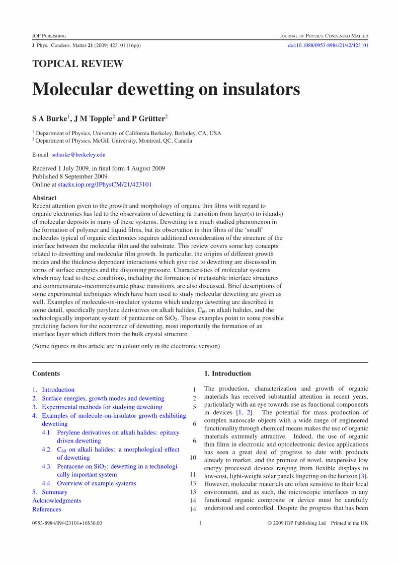
Figure 7. (a) Nc-AFM image of a C60 island on KBr with branchedmorphology exhibiting disconnected regions, enclosed monolayerareas and wrapped branches [21]. (b) SEM and (c) AFM of peryleneon Cu(110) showing the similar ‘skeleton’ morphology as a result ofdewetting [14]. (b) and (c) reprinted with permission from [14].Copyright (2006) by Springer Science + Business Media.
strain, which propagates with thickness, can also be consideredas a structural component of the disjoining pressure whichleads to dewetting. In describing the dynamics of PTCDIon NaCl dewetting a monomolecular growth model andanalogous decay function was used to empirically fit the islandpopulations as a function of time [24]. Also, perhaps importantfor the description of molecular dewetting dynamics, is that thebackground concentration field is not constant with time butdecreases as the finite number of particles are consumed by thestable island population.
4.2. C60 on alkali halides: a morphological effect of dewetting
Growth of C60 fullerene molecules and fullerene derivativesin submonolayer coverages and thin films [80, 54, 55, 59, 81]has received considerable attention in recent years due to theirinteresting electronic and optoelectronic properties [82–84].There have been several studies of C60 growth on alkalihalides [80, 85–87] primarily with the aim of achieving largesingle crystal films on these weakly interacting substrates. Atroom temperature, submonolayer coverages of C60 on KBrand NaCl were found by nc-AFM to exhibit unique dendriticisland shapes which appear to be a result of a dewettingprocess [62, 21].
The dendritic island shapes observed for C60 on KBrand NaCl have some unique features which are not generallyobserved for ‘hit and stick’ growth processes that result indendritic island shapes [88]. The islands observed often exhibitbranches which wrap back towards the centre of the island, andsometimes consist of several disconnected regions which havethe same orientation and are localized in the same area (seefigure 7(a)). Also, these islands consist of rims of two layers of
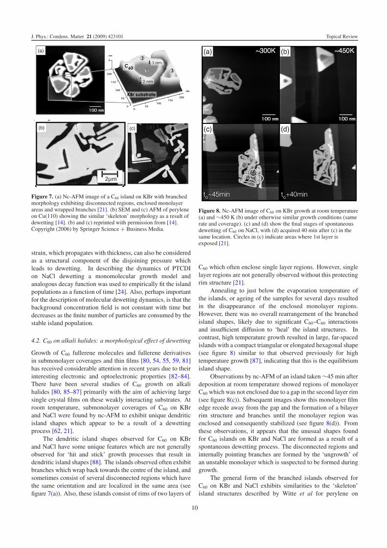
Figure 8. Nc-AFM image of C60 on KBr growth at room temperature(a) and ∼450 K (b) under otherwise similar growth conditions (samerate and coverage). (c) and (d) show the final stages of spontaneousdewetting of C60 on NaCl, with (d) acquired 40 min after (c) in thesame location. Circles in (c) indicate areas where 1st layer isexposed [21].
C60 which often enclose single layer regions. However, singlelayer regions are not generally observed without this protectingrim structure [21].
Annealing to just below the evaporation temperature ofthe islands, or ageing of the samples for several days resultedin the disappearance of the enclosed monolayer regions.However, there was no overall rearrangement of the branchedisland shapes, likely due to significant C60–C60 interactionsand insufficient diffusion to ‘heal’ the island structures. Incontrast, high temperature growth resulted in large, far-spacedislands with a compact triangular or elongated hexagonal shape(see figure 8) similar to that observed previously for hightemperature growth [87], indicating that this is the equilibriumisland shape.
Observations by nc-AFM of an island taken ∼45 min afterdeposition at room temperature showed regions of monolayerC60 which was not enclosed due to a gap in the second layer rim(see figure 8(c)). Subsequent images show this monolayer filmedge recede away from the gap and the formation of a bilayerrim structure and branches until the monolayer region wasenclosed and consequently stabilized (see figure 8(d)). Fromthese observations, it appears that the unusual shapes foundfor C60 islands on KBr and NaCl are formed as a result of aspontaneous dewetting process. The disconnected regions andinternally pointing branches are formed by the ‘ungrowth’ ofan unstable monolayer which is suspected to be formed duringgrowth.
The general form of the branched islands observed forC60 on KBr and NaCl exhibits similarities to the ‘skeleton’island structures described by Witte et al for perylene on
10

J. Phys.: Condens. Matter 21 (2009) 423101 Topical Review
Figure 9. Preferred lattice sites for C60 on KBr determined fromcalculations (left) [90, 91, 45] and comparison with measuredexperimental lattice showing small contraction of lattice from thisideal adsorption epitaxy.
Cu(110) which were also formed by dewetting (see figures 7(b)and (c)) [14]. In particular, the appearance of rimmedstructures with wide branches and holes which maintain thesymmetry of the molecular crystal is consistent with theappearance of branched C60 islands. While for the caseof perylene on Cu(110), dewetting is induced by annealing,for C60 on KBr and NaCl the process occurs spontaneouslyfollowing growth [21], presumably due to the kinetic trappingof a monolayer structure during deposition similar to the caseof PTCDI on NaCl [24] discussed above but on a fastertimescale.
Phase field modelling of the C60 growth on alkalihalides [89] was used to investigate island shape formation.A free energy consisting of a triple well representing thebare substrate, a metastable monolayer and a stable secondlayer was used. Given the correct parameters, a ‘growth’period resulted in hexagonal monolayer islands which duringan ‘evolution’ period were shown to evolve into islandswith bilayer rims and interior monolayers or bilayer regionswith interior holes. A variety of branched and disconnectedstructures could also be achieved by initiating the evolutionperiod with notches or fluctuations in the edge density. Therather striking reproduction of the island shapes indicates thatthe formation of the branched island structures is a resultof a dewetting process and that the variety of shapes areformed as a result of random variations in the initial shapeof the monolayer island and/or fluctuations in the edges whendewetting begins.
Considering the molecular epitaxy once more, theobserved bilayer and trapped monolayers were found to havea large coincident unit cell containing 142 molecules on KBr.Since the initial monolayer was not stable, the epitaxy for thisstate was not observed. However, comparing to calculatedadsorption sites for C60 on KBr [91, 45], a similar, butcommensurate lattice was found (see figure 9) [90]. Theobserved lattice is smaller than the lattice of favourableadsorption sites, and is closer to the C60–C60 equilibriumdistance [46]. Much like PTCDA, the commensurate latticeresults in a strain in the molecular lattice that is likelyallowable, however, intermolecular interactions appear toovercome the influence of the adsorption potential and the
Figure 10. XPS intensity as a function of time after deposition fordifferent film thickness and substrate temperatures. Reprinted withpermission from [12]. Copyright (2009) by Springer Science +Business Media.
Figure 11. (a) Spacefill model of pentacene (hydrogen atoms notshown), (b)–(d) schematic representation of monolayer, thin filmphase and bulk phase orientation of molecules with respect to thesubstrate (based on [6, 97]).
resulting balance between these competing interactions givesthe experimentally observed lattice. One may speculate thatduring growth the C60 molecules form a lattice correspondingto the favourable adsorption sites, but that this lattice isunstable and spontaneously dewets, altering the interface andgiving the observed epitaxy.
C60 on alkali halides undergoes a spontaneous dewettingprocess resulting in an unusual branched island morphology.This is likely driven by competition between commensurateand coincident lattices similar to that observed for perylenederivatives. Further work characterizing the morphologyand evolution during and immediately following depositionto characterize the unstable monolayer would be of interestfor understanding the origin and stability of the early-time structures and characterizing this spontaneous dewettingprocess.
4.3. Pentacene on SiO2: dewetting in a technologicallyimportant system
The thin film growth of pentacene is of considerabletechnological interest due its use as a prototypical organicsemiconductor and its superior performance in thin film FETdevices [92–94]. Thin films of pentacene, a planar moleculeconsisting of a five aromatic rings arranged in a line (see
11

J. Phys.: Condens. Matter 21 (2009) 423101 Topical Review
figure 11(a)), form a herringbone structure much like thebulk crystal with molecules arranged such that they are nearlyperpendicular to the surface with only a small tilt angle relativeto the surface normal (see figure 11(d)). Typically, pentacenethin films on SiO2 are well ordered, though polycrystalline.Since the charge transport is believed to occur within the firstfew molecular layers adjacent to the dielectric interface inOTFTs [4–6], these devices are very often sensitive to interfacestructure. The use of organic self-assembled monolayers(SAMs) to tune the interface of pentacene OTFTs has beenexplored [95, 96, 2, 7] and the effect of SAM modificationon growth of pentacene thin films has also been examined anddiscussed in terms of surface energy modification [16].
A recent study of pentacene growth on SiO2 andAu(111) performed by Kafer et al [12] reported evidenceof significant post-deposition dewetting on both of thesesubstrates. On SiO2, layer-by-layer growth is initially observedwith the first monolayer nearly completed before subsequentlayer formation, followed by substantial roughening. XPSmeasurements of the C 1s peak and the Si 2p were usedto monitor the area covered by pentacene islands (islandbase area) versus the area of the exposed SiO2 substrate,respectively. This was done during growth, during annealing,and post-deposition. Deposition at low temperatures (200 K)resulted in homogeneous pentacene films which were thenannealed and monitored for changes in the proportion of thesurface which was covered by pentacene (the island basearea). No significant rapid change was observed until ∼325 K.Interestingly, at similar temperatures, a significant changein the pentacene island morphology measured by AFM wasalso observed, changing from pyramidal islands to block-likedendritic islands. The authors note that since a phase transitionoccurs in this same range from the ‘thin film’ phase to themore tilted bulk phase that this morphological change maybe accompanied by a crystallographic rearrangement of thepentacene molecules in the film [12].
Of particular note, is the evolution of the pentacene filmafter deposition even at temperatures below this annealingtransition. The XPS signals here again correspond to areduction in the area covered by pentacene occurring overthe course of some 10s of minutes following deposition (seefigure 10). Since desorption can be excluded by thermallyprogrammed desorption (TPD) data, this again must beattributed to a substantial rearrangement of the film. Theintensity versus time curves were empirically fit to a sigmoidalWeibull function, representing a smooth exponential transitionfrom one state to the other, and permitting a quantitativecharacterization of the timescale involved in the dewettingdynamics much as in the case of PTCDI on NaCl. Withincreased temperature, the pentacene film exhibits the sameprocess occurring on a faster timescale, indicating a thermallyactivated process. Film thickness was also shown to playa role, with thicker films evolving more slowly due to thelarger amount of material involved in this rearrangement. Itshould be noted that similar dynamics were observed forpentacene on Au(111), although in that case the first monolayeris chemisorbed and remains post-dewetting. No stronglyadsorbed monolayer was observed from the TPD spectra takenfor pentacene on SiO2 [12].
The temporal evolution and thermally induced changes ofthese pentacene films raise potential questions about thermaland long-term stability of thin film pentacene devices on SiO2,as well as other similar systems. This highlights the importanceof tracking device characteristics over relevant timescales andexploring temperature tolerances of organic thin films fortechnological applications. Additionally, exploration of filmsduring and immediately prior to growth can give insight intohow to better control the final film morphology, especiallywhere dewetting is concerned.
The structure of vacuum deposited pentacene thin filmson SiO2 has also been examined in order to better understandand improve device characteristics [6, 97]. A recentstudy by Mannsfeld et al utilizing grazing incidence x-ray diffraction (GIXD) has addressed the structure in greatdetail [6] (see article for experimental details and structurerefinement methods). Of particular interest in this study, is thedetermination of a monolayer structure which differs from the‘thin film’ phase. While both exhibit the herringbone latticewhich is similar to the bulk crystal structure, the pentacenemolecules of the first monolayer was found to stand exactlyperpendicular to the SiO2 substrate with an a–b unit cell that issignificantly smaller than either the thin film phase or the bulkcrystal. As the thickness of the film is increased, the thin filmphase is observed with a tilt angle that is ∼5◦–6◦ with respectto the surface normal and lattice constants that are more similarto the bulk pentacene crystal.
Also of particular relevance for organic thin film devices,calculations indicated that the transport through this monolayerstructure differs from the ‘thin film’ tilted phase. Due tothe change in symmetry between the edge–face interactions,charge transport should be improved for this configuration [6].This emphasizes the importance of understanding the detailedstructure of molecular films at the dielectric interface assmall changes in the structure may influence device-relatedproperties.
It may be that the monolayer phase of pentacene wets thesurface, due to a stronger molecule–substrate interaction, butis not compatible with thicker film growth much like the caseof PTCDA on NaCl and KCl. Given sufficient energy and/ortime, this film may reconstruct to the thin film phase, or if givenfurther energy (T > 340 K) even the bulk phase resulting in adifferent morphology. There are still open questions remainingregarding the stability and structure of this technologicallyimportant system, and additional characterization of theinterface structure and dynamics both during and after growthare required as well as detailed modelling which can capturethe potentially important changes at the molecular scale inconjunction with large scale morphological rearrangements.
Modification of gate dielectric surfaces through the useof self-assembled monolayers (SAMs) is sometimes usedin organic electronics to tune dielectric properties, surfaceenergy, interface structure, or a combination thereof (see forexample [95, 96, 2, 7]). A recent investigation by Amassianet al [16] investigates growth and post-deposition behaviour ofpentacene thin films on SiO2, hexamethyldisilazane (HDMS)modified SiO2, and fluorinated octyltrichlorosilane (FOTS)modified SiO2 using in situ time resolved x-ray reflectivity
12

J. Phys.: Condens. Matter 21 (2009) 423101 Topical Review
(TR-XRR) and ex situ AFM. TR-XRR measurements duringgrowth indicate similar progression of the film structure on allthree surfaces, with a nearly complete first layer in all cases,and subsequent roughening of the film. AFM measurementsshow significant post-deposition dewetting of thin films ofpentacene on the SAM modified substrates. In these cases,the AFM data shows the initiation of holes or pits adjacentto islands, indicating growth of islands through mass transportfrom the interface layer in a situation similar to that observedfor PTCDA on NaCl [22]. While in this study no dewetting wasobserved for pentacene on bare SiO2, contrary to the resultsdescribed above, subtle differences between experimentalconditions, including deposition method, may influence theformation and structure of the interface layer which is expectedto dictate the occurrence of dewetting. Rearrangement ofthe films was also not observed for coverages of more than∼5 ML, indicating that any re-organization necessary hasalready occurred during growth, or that the buried interfacebecomes trapped and can no longer rearrange. Interestingly,re-organization was also not observed for films on HDMSand FOTS modified SiO2 which were exposed to an ambientenvironment, indicating that this exposure to air may passivatehole nucleation sites and stabilize the films. However, sinceexposure to air is generally considered detrimental to theperformance of organic thin film devices, the evolution of thesefilms in inert environments remains of substantial importance.
4.4. Overview of example systems
In the examples described here there are two maincommonalities: a morphological transition occurs which isaccompanied by, and most likely driven by, a change in theinterface structure. The dewetting transitions observed forperylene derivatives on alkali halides provide the most strikingexample of this with an apparent change in epitaxy for severalof these systems from commensurate layer(s) to islands withbulk-like lattice parameters [22, 23] much like the simple1D example illustrated in figure 2. However, as seen in thecase of PTCDA on KBr, when near lattice matching occursbetween the molecular overlayer and substrate, dewetting is notobserved despite similar bulk surface energies. Comparing themeasured experimental lattice observed after dewetting to the‘ideal’ adsorption lattice determined from calculated minimumenergy adsorption sites, a similar effect may also occur for C60
on alkali halides. Lastly, while it remains somewhat unclearfor pentacene on SiO2 as the detailed structure and observationof dewetting have not appeared in a single unified study, thedewetting transition observed for this system may arise fromthe different structure observed for monolayer pentacene whichhas both a different tilt angle and lattice constants than eitherthe ‘thin film’ or bulk phases [6].
The formation of metastable films with lattices differingfrom the anticipated bulk molecular crystals gives rise tothe thickness dependant interactions, which are prerequisitefor dewetting. In cases where the surface energies of thedeposit and substrate are similar, the growth mode will beprimarily dictated by the interface energy and these thicknessdependent interactions making these systems particularly
likely to undergo dewetting as appears to be the case for manymolecule on insulator systems. In these situations, examinationof lattice mismatch, or the molecular arrangements of thin filmstructures may provide a predictor of whether or not dewettingwill occur.
Lastly, it should be noted that in two of the systemsdiscussed, branched structures are formed as a result ofdewetting. The thick branches which occur for PTCDA onNaCl form as a result of the haphazard addition of materialfrom nearby dewetting monolayer islands [73]. C60 on alkalihalides exhibits very unique branched structures, which areremarkably stable once formed [21]. These shapes may arisefrom the amplification of fluctuations during the spontaneousdewetting process in the so-called ‘spinodal’ regime. In bothcases, the equilibrium shapes formed through either annealingor high substrate temperature depositions, differ significantly,indicating that films which undergo dewetting may have verydifferent morphology as a result of this process.
5. Summary
The process of dewetting is well known for liquids andpolymers, whereby a film is broken up and transformed intodroplets or crystallites. Recent studies indicate that this appliesalso to organic crystalline films deposited in vacuum, andmay even be relatively common. The thickness dependentfree energy, also termed the disjoining pressure, is a requisitefor dewetting and arises from a combination of long rangemolecule–substrate forces and structuring of the crystallinefilm, and are specific to the system under consideration asthese ultrathin films are often of molecular dimension. Theexamples described here exhibit dewetting due to a changein the molecule–substrate interface structure, specifically analteration of the epitaxial relation and/or a change in themolecular orientation at the interface. The occurrence ofdewetting in organic films appears to be particularly prevalenton insulating, or otherwise low surface energy, surfaces dueto a close competition of the surface energies of the two bulkmaterials, as well as a close competition between adsorptionand intermolecular interactions. Since many organic materialshave low surface energies, including polymer materials,this may also have consequences for organic thin films on‘plastics’. Additionally, the compliance of organic materialsfurther accommodates substrate induced strains leading tothe easy formation of multiple epitaxies. These readilyformed different interface structures can give rise to thicknessdependent interaction providing the conditions for dewetting.
Further study of dewetting molecular systems where thedetails of the interface structure as well as the film evolutionduring growth and post-deposition re-organization of films areall known will continue to increase our understanding of thedriving forces and necessary conditions for dewetting. Thedevelopment of a predictive framework through the analysis ofsuch experiments and detailed modelling from the molecularscale to the large scale film morphology will further ourunderstanding of stability and morphology of organic films.Theoretical treatment of these systems, spanning the molecularscale to relevant film morphology scales, characterizing the
13

J. Phys.: Condens. Matter 21 (2009) 423101 Topical Review
energetic conditions which predispose dewetting of organicfilms and the dependence of the stability on molecular scaleprocesses is needed. Calculation of the disjoining pressure forsome of these ‘prototypical’ dewetting systems would be ofinterest to elucidate the key parameters which drive and controldewetting. Experimentally, molecular mobility (diffusion)may be altered by varying the substrate temperature, whichchanges the rate of dewetting as well as the final islandsize. The appearance of post-deposition temporal evolutiondata, like that highlighted in the examples here, should helpto provide a basis for theory, however more studies likethese carefully quantifying dewetting dynamics and stabilityare needed. This will allow for the engineering of higherquality organic thin films and may serve to increase theperformance of future organic thin film devices. Furthermore,investigation of how dewetting is influenced by substratestructures may lead to new methods for creating controllednanostructured deposits of molecular materials, similar to thatshown for gold on structured Si/SiO2 [74]. This approachmay apply particularly well to insulating surfaces which canbe structured by a number of means [98] and where nanoscalepits on alkali halides have already been shown to template thegrowth of molecules [63, 64, 26]. Methods of tuning filmmorphology and the rate of dewetting through total coverage,surface templating and temperature control are currently underinvestigation. Preliminary results for PTCDI on NaCl indicatethat the resultant island density, size, and rate of dewettingmay be tuned by templating the substrate with single atomicdepth pits, depositing gold nanoclusters, or a combinationof the two to modify nucleation. The characterization ofparameters and conditions which stabilize metastable filmsor interface structures will be of great importance so thatnovel properties of films of this nature can be utilized intechnological applications.
Acknowledgments
The authors would like to thank Wei Ji and Hong Guo,Quonyong Wang, Dan Vernon and Martin Grant, and AramAmassian for providing advance copies of manuscripts inprocess. The authors would also like to thank JeffreyMativetsky, Shawn Fostner, Jeffrey LeDue, Roland Bennewitzand Jorge Vinals for discussions. The following fundingagencies are gratefully acknowledged for their support:NSERC, CFI, FQRNT, CIfAR, CMP and RQMP.
References
[1] Forrest S R 1997 Ultrathin organic films grown by organicmolecular beam deposition and related techniques Chem.Rev. 97 1793–896
[2] Liu S H, Wang W C M, Briseno A L, Mannsfeld S C E andBao Z N 2009 Controlled deposition of crystalline organicsemiconductors for field-effect-transistor applications Adv.Mater. 21 1217–32
[3] Forrest S R 2004 The path to ubiquitous and low-cost organicelectronic appliances on plastic Nature 428 911–8
[4] Dimitrakopoulos C D and Malenfant P R L 2002 Organic thinfilm transistors for large area electronics Adv. Mater. 14 99
[5] Karl N 2003 Charge carrier transport in organic semiconductorsSynth. Met. 133/134 649–57
[6] Mannsfeld S C B, Virkar A, Reese C, Toney M F andBao Z 2009 Precise structure of pentacene monolayers onamorphous silicon oxide and relation to charge transportAdv. Mater. 21 2294
[7] Braga D and Horowitz G 2009 High-performance organicfield-effect transistors Adv. Mater. 21 1473–86
[8] Witte G and Woll C 2004 Growth of aromatic molecules onsolid substrates for applications in organic electronicsJ. Mater. Res. 19 1889–916
[9] Schreiber F 2004 Organic molecular beam deposition: growthstudies beyond the first monolayer Phys. Status Solidi a201 1037–54
[10] Beernink G, Strunskus T, Witte G and Woll C 2004 Importanceof dewetting in organic molecular-beam deposition:pentacene on gold Appl. Phys. Lett. 85 398–400
[11] Kafer D, Ruppel L and Witte G 2007 Growth of pentacene onclean and modified gold surfaces Phys. Rev. B 75 085309
[12] Kafer D, Woll C and Witte G 2009 Thermally activateddewetting of organic thin films: the case of pentacene onSiO2 and gold Appl. Phys. A 95 273–84
[13] Krause B, Durr A C, Schreiber F, Dosch H and Seeck O H2003 Thermal stability and partial dewetting of crystallineorganic thin films: 3,4,9,10-perylenetetracarboxylicdianhydride on Ag(111) J. Chem. Phys. 119 3429–35
[14] Witte G, Hanel K, Sohnchen S and Woll C 2006 Growth andmorphology of thin films of aromatic molecules on metals:the case of perylene Appl. Phys. A 82 447–55
[15] Frank P, Koch N, Koini M, Rieger R, Mullen K, Resel R andWinkler A 2009 Layer growth and desorption kinetics of adiscoid molecular acceptor on Au(111) Chem. Phys. Lett.473 321–5
[16] Amassian A, Pozdin V A, Desai T V, Hong S, Woll A R,Ferguson J D, Brock J D, Malliaras G G andEngstrom J R 2009 Post deposition reorganization ofpentacene films deposited on low-energy surfaces J. Mater.Chem. 19 5580–92
[17] Rath S and Port H 2006 Dewetting of thin UHV-depositedorganic films Chem. Phys. Lett. 421 152–6
[18] Tang Y H, Wang Y, Wang G, Wang H B, Wang L X andYan D H 2004 Vacuum-deposited submonolayer thin filmsof a three-ring bent-core compound J. Phys. Chem. B108 12921–6
[19] Durr A C, Schreiber F, Ritley K A, Kruppa V, Krug J,Dosch H and Struth B 2003 Rapid roughening in thin filmgrowth of an organic semiconductor (diindenoperylene)Phys. Rev. Lett. 90 016104
[20] Zhang X N, Barrena E, de Oteyza D G and Dosch H 2007Transition from layer-by-layer to rapid roughening in thegrowth of DIP on SiO2 Surf. Sci. 601 2420–5
[21] Burke S A, Mativetsky J M, Fostner S and Grutter P 2007C60 on alkali halides: epitaxy and morphology studied bynoncontact AFM Phys. Rev. B 76 035419
[22] Burke S A, Ji W, Mativetsky J M, Topple J M, Fostner S,Gao H-J, Guo H and Grutter P 2008 Strain induceddewetting of a molecular system: bimodal growth of PTCDAon NaCl Phys. Rev. Lett. 100 186104
[23] Dienel T, Loppacher C, Mannsfeld S C B, Forker R andFritz T 2008 Growth-mode-induced narrowing of opticalspectra of an organic adlayer Adv. Mater. 20 959
[24] Topple J M, Burke S A, Fostner S and Grutter P 2009 Thin filmevolution: dewetting dynamics of a bimodal molecularsystem Phys. Rev. B 79 205414
[25] Fendrich M, Lange M, Weiss C, Kunstmann T andMoller R 2009 N,n′-dimethylperylene-3,4,9,10-bis(dicarboximide) on alkali halide (001) surfaces J. Appl.Phys. 105 094311
[26] Burke S A, LeDue J M, Topple J M, Fostner S andGrutter P 2009 Organic semiconductors: relating thefunctional properties of an organic semiconductor tomolecular structure by nc-AFM Adv. Mater. 21 2029–33
14

J. Phys.: Condens. Matter 21 (2009) 423101 Topical Review
[27] Venables J A 2000 Introduction to Surface and Thin FilmProcesses (Cambridge: Cambridge University Press)
[28] Zangwill A 1988 Physics at Surfaces (Cambridge: CambridgeUniversity Press)
[29] Israelachvili J 1991 Intermolecular and Surface Forces 2nd edn(London: Academic)
[30] deGennes P-G, Brochard-Wyart F and Quere D 2004Capillarity and Wetting Phenomena: Drops, Bubbles,Pearls, Waves (New York: Springer)
[31] deGennes P G 1985 Wetting—statics and dynamics Rev. Mod.Phys. 57 827–63
[32] Thiele U 2003 Open questions and promising new fields indewetting Eur. Phys. J. E 12 409–16
[33] Kim H I, Mate C M, Hannibal K A and Perry S S 1999 Howdisjoining pressure drives the dewetting of a polymer film ona silicon surface Phys. Rev. Lett. 82 3496–9
[34] Reiter G 1993 Unstable thin polymer-films—rupture anddewetting processes Langmuir 9 1344–51
[35] Bonn D, Eggers J, Indekeu J, Meunier J and Rolley E 2009Wetting and spreading Rev. Mod. Phys. 81 739–805
[36] Thurmer K, Williams E D and Reutt-Robey J E 2003 Dewettingdynamics of ultrathin silver films on Si(111) Phys. Rev. B68 155423
[37] Derjaguin B V and Churaev N V 1974 Structural component ofdisjoining pressure J. Colloid Interface Sci. 49 249–55
[38] Mitlin V S 1993 Dewetting of solid-surface—analogy withspinodal decomposition J. Colloid Interface Sci. 156 491–7
[39] Hooks D E, Fritz T and Ward M D 2001 Epitaxy and molecularorganization on solid substrates Adv. Mater. 13 227
[40] Koch S W, Rudge W E and Abraham F F 1984 Thecommensurate incommensurate transition of krypton ongraphite—a study via computer-simulation Surf. Sci.145 329–44
[41] Kowarik S, Gerlach A and Schreiber F 2008 Organic molecularbeam deposition: fundamentals, growth dynamics, and insitu studies J. Phys.: Condens. Matter 20 184005
[42] Stohr M, Gabriel M and Moller R 2002 Investigation of thegrowth of PTCDA on Cu(110): an STM study Surf. Sci.507 330–4
[43] Ji W, Lu Z-Y and Gao H 2006 Electron core–hole interactionand its induced ionic structural relaxation in molecularsystems under x-ray irradiation Phys. Rev. Lett. 97 246101
[44] Ji W, Lu Z-Y and Gao H-J 2008 Multichannel interactionmechanism in a molecule–metal interface Phys. Rev. B77 113406–4
[45] Ji W, Burke S A, Gao H-J, Grutter P and Guo H 2009Electronic hybridization of molecules on insulating surfacessubmitted
[46] Girifalco L A 1992 Molecular properties of C60 in the gas andsolid phases J. Phys. Chem. 96 858–61
[47] Northrup J E, Tiago M L and Louie S G 2002 Surfaceenergetics and growth of pentacene Phys. Rev. B 66121404(R)
[48] Vanzeggeren F and Benson G C 1957 Calculation of the surfaceenergies of alkali halide crystals J. Chem. Phys. 26 1077–82
[49] Knieling T, Lang W and Benecke W 2007 Gas phasehydrophobisation of MEMS silicon structures withself-assembling monolayers for avoiding in-use stickingSensors Actuators B 126 13–7
[50] Kawai A and Kawakami J 2003 Characterization of SiO2surface treated by HMDS vapor and O2 plasma with AFMtip J. Photopolym. Sci. Technol. 16 665–8
[51] Tyson W R and Miller W A 1977 Surface free-energies of solidmetals—estimation from liquid surface-tensionmeasurements Surf. Sci. 62 267–76
[52] Da Silva J L F, Stampfl C and Scheffler M 2006 Convergedproperties of clean metal surfaces by all-electronfirst-principles calculations Surf. Sci. 600 703–15
[53] Glockler K, Seidel C, Soukopp A, Sokolowski M, Umbach E,Bohringer M, Berndt R and Schneider W D 1998 Highlyordered structures and submolecular scanning tunnellingmicroscopy contrast of PTCDA and DM-PBDCI monolayerson Ag(111) and Ag(110) Surf. Sci. 405 1–20
[54] Grobis M, Lu X and Crommie M F 2002 Local electronicproperties of a molecular monolayer: C60 on Ag(001) Phys.Rev. B 66 161408
[55] Lu X H, Grobis M, Khoo K H, Louie S G and Crommie M F2003 Spatially mapping the spectral density of a single C60molecule Phys. Rev. Lett. 90 096802
[56] Swarbrick J C, Ma J, Theobald J A, Oxtoby N S, O’Shea J N,Champness N R and Beton P H 2005 Square, hexagonal, androw phases of PTCDA and PTCDI on Ag-Si(111)root 3×root 3r30 degrees J. Phys. Chem. B 109 12167–74
[57] Swarbrick J C, Rogers B L, Champness N R and Beton P H2006 Hydrogen-bonded PTCDA-melamine networks andmixed phases J. Phys. Chem. B 110 6110–4
[58] Rosei F, Schunack M, Naitoh Y, Jiang P, Gourdon A,Laegsgaard E, Stensgaard I, Joachim C andBesenbacher F 2003 Properties of large organic moleculeson metal surfaces Prog. Surf. Sci. 71 95–146
[59] Pradhan N A, Liu N and Ho W 2005 Vibronic spectroscopy ofsingle C60 molecules and monolayers with the STM J. Phys.Chem. B 109 8513
[60] Repp J, Meyer G, Paavilainen S, Olsson F E andPersson M 2006 Imaging bond formation between a goldatom and pentacene on an insulating surface Science312 1196–9
[61] Yamada H, Fukuma T, Umeda K, Kobayashi K andMatsushige K 2002 Local structures and electrical propertiesof organic molecular films investigated by non-contactatomic force microscopy Appl. Surf. Sci. 188 391–8
[62] Burke S A, Mativetsky J M, Hoffmann R and Grutter P 2005Nucleation and submonolayer growth of C60 on KBr Phys.Rev. Lett. 94 096102
[63] Nony L, Gnecco E, Baratoff A, Alkauskas A, Bennewitz R,Pfeiffer O, Maier S, Wetzel A, Meyer E and Gerber C 2004Observation of individual molecules trapped on ananostructured insulator Nano Lett. 4 2185–9
[64] Mativetsky J M, Burke S A, Fostner S and Grutter P 2007Templated growth of 3,4,9,10-perylenetetracarboxylicdianhydride molecules on a nanostructured insulatorNanotechnology 18 105303
[65] Maier S, Fendt L A, Zimmerli L, Glatzel T, Pfeiffer O F,Diederich F and Meyer E 2008 Nanoscale engineering ofmolecular porphyrin wires on insulating surfaces Small4 1115–8
[66] Albrecht T R, Grutter P, Horne D and Rugar D 1991Frequency-modulation detection using high-Q cantileversfor enhanced force microscope sensitivity J. Appl. Phys.69 668–73
[67] Wagner T, Bannani A, Bobisch C, Karacuban H, Stohr M,Gabriel M and Moller R 2004 Growth of3,4,9,10-perylenetetracarboxylic-dianhydride crystallites onnoble metal surfaces Org. Electron. 5 35–43
[68] Gustafsson J B, Zhang H M and Johansson L S O 2007 STMstudies of thin PTCDA films on Ag/Si(111)-
√3 × √
3 Phys.Rev. B 75 155414
[69] Schlettwein D, Back A, Schilling B, Fritz T and Armstrong N R1998 Ultrathin films of perylenedianhydride andperylenebis(dicarboximide) dyes on (001) alkali halidesurfaces Chem. Mater. 10 601–12
[70] Seidel C, Awater C, Liu X D, Ellerbrake R and Fuchs H 1997A combined STM, LEED and molecular modelling study ofPTCDA grown on Ag(110) Surf. Sci. 371 123–30
[71] Ogawa T, Kuwamoto K, Isoda S, Kobayashi T and Karl N 19993,4:9,10-perylenetetracarboxylic dianhydride (PTCDA) byelectron crystallography Acta Crystallogr. B 55 123–30
[72] Silly F and Castell M R 2006 Bimodal growth of Au on SrTiO3(001) Phys. Rev. Lett. 96 086104
[73] Burke S A 2009 Building foundations for molecularelectronics: growth of organic molecules on alkali halides asprototypical insulating substrates PhD Thesis McGillUniversity, Montreal, Canada Can be retrieved throughhttp://digitool.library.mcgill.ca:8881/R/
[74] Giermann A L and Thompson C V 2005 Solid-state dewettingfor ordered arrays of crystallographically oriented metalparticles Appl. Phys. Lett. 86 121903
15

J. Phys.: Condens. Matter 21 (2009) 423101 Topical Review
[75] Kunstmann T, Schlarb A, Fendrich M, Wagner T, Moller R andHoffmann R 2005 Dynamic force microscopy study of3,4,9,10-perylenetetracarboxylic dianhydride on KBr(001)Phys. Rev. B 71 121403(R)
[76] Tojo K and Mizugushi J 2002 Refinement of the crystalstructure of 3,4:9,10-perylene-bis(dicarboximide),C24H10N2O4, at 263 K Z. Kristallogr. 217 45 (Data depositedat the Cambridge Crystallographic Data center (CCDC) File:LENPEZ01, No. CCDC 187633)
[77] Guillermet O, Mossoyan-Deneux M, Giorgi M, Glachant A andMossoyan J C 2006 Structural study of vapour phasedeposited 3,4,9,10-perylene tetracarboxylicacid diimide:comparison between single crystal and ultra thin films grownon Pt(100) Thin Solid Films 514 25–32
[78] Harris L A and Clancy P 2006 A ‘partitioned leaping’ approachfor multiscale modeling of chemical reaction dynamicsJ. Chem. Phys. 125 144107
[79] Choudhary D, Clancy P, Shetty R and Escobedo F 2006A computational study of the sub-monolayer growth ofpentacene Adv. Funct. Mater. 16 1768–75
[80] Luthi R, Haefke H, Meyer E, Howald L, Lang H P,Gerth G and Guntherodt H J 1994 Frictional andatomic-scale study of C60 thin-films by scanning forcemicroscopy Z. Phys. B 95 1–3
[81] Cavar E, Blum M C, Pivetta M, Patthey F, Chergui M andSchneider W D 2005 Fluorescence and phosphorescencefrom individual C-60 molecules excited by local electrontunneling Phys. Rev. Lett. 95 196102
[82] Joachim C and Gimzewski J K 1997 An electromechanicalamplifier using a single molecule Chem. Phys. Lett.265 353–7
[83] Dresselhaus M S, Dresselhaus G and Eklund P C 1993Fullerenes J. Mater. Res. 8 2054–97
[84] Segura J L, Martin N and Guldi D M 2005 Materials fororganic solar cells: the C60/pi-conjugated oligomerapproach Chem. Soc. Rev. 34 31–47
[85] Tanigaki K, Kuroshima S and Ebbesen T W 1995Crystal-growth and structure of fullerene thin-films ThinSolid Films 257 154–65
[86] Yase K, Ara-Kato N, Hanada T, Takiguchi H, Yoshida Y,Back G, Abe K and Tanigaki N 1998 Aggregation
mechanism in fullerene thin films on several substrates ThinSolid Films 331 131–40
[87] Kim Y, Jiang L, Iyoda T, Hashimoto K and Fujishima A 1998AFM study of surface phenomena based on C60 film growthAppl. Surf. Sci. 130 602–9
[88] Zhang Z Y and Lagally M G 1997 Atomistic processes in theearly stages of thin-film growth Science 276 377–83
[89] Wang Q, Vernon D and Grant M, Multilayer surface growth andphysisorption on insulating substrate submitted, privatecommunication
[90] Ji W, private communication[91] Jung S C and Kang M H 2008 First-principles study of a single
C60 cluster adsorbed on KBr(100) Surf. Sci. 602 1916–20[92] Shtein M, Mapel J, Benziger J B and Forrest S R 2002 Effects
of film morphology and gate dielectric surface preparationon the electrical characteristics of organic-vapor-phase-deposited pentacene thin-film transistors Appl. Phys. Lett.81 268–70
[93] Klauk H, Halik M, Zschieschang U, Schmid G, Radlik W andWeber W 2002 High-mobility polymer gate dielectricpentacene thin film transistors J. Appl. Phys. 92 5259–63
[94] Reese C, Chung W J, Ling M M, Roberts M and Bao Z N 2006High-performance microscale single-crystal transistors bylithography on an elastomer dielectric Appl. Phys. Lett.89 202108
[95] McDowell M, Hill I G, McDermott J E, Bernasek S L andSchwartz J 2006 Improved organic thin-film transistorperformance using novel self-assembled monolayers Appl.Phys. Lett. 88 073505
[96] Hill I G, Weinert C M, Kreplak L and van Zyl B P 2009Influence of self-assembled monolayer chain length onmodified gate dielectric pentacene thin-film transistors Appl.Phys. A 95 81–7
[97] Schiefer S, Huth M, Dobrinevski A and Nickel B 2007Determination of the crystal structure of substrate-inducedpentacene polymorphs in fiber structured thin films J. Am.Chem. Soc. 129 10316
[98] Bennewitz R 2006 Structured surfaces of wide band gapinsulators as templates for overgrowth of adsorbatesJ. Phys.: Condens. Matter 18 R417–35
16


![Thickness-dependent spontaneous dewetting morphology of ...people.wku.edu/mikhail.khenner/LaserPattAg.pdfheterogeneous nucleation or spinodal dewetting [23]. In the case of homogeneous](https://static.fdocuments.us/doc/165x107/60ee61d71c1e3b20b84c0cd4/thickness-dependent-spontaneous-dewetting-morphology-of-heterogeneous-nucleation.jpg)


![Power-law scaling for solid-state dewetting of thin films: an ...arXiv:2001.09331v1 [cond-mat.mtrl-sci] 25 Jan 2020 Power-law scaling for solid-state dewetting of thin films: an](https://static.fdocuments.us/doc/165x107/5f9fb055509d0c5e633b296a/power-law-scaling-for-solid-state-dewetting-of-thin-ilms-an-arxiv200109331v1.jpg)