Molecular beam epitaxial growth of GaSb/GaAs quantum dots on Ge substrates
4
Molecular beam epitaxial growth of GaSb/GaAs quantum dots on Ge substrates Maetee Kunrugsa a , Suwit Kiravittaya b , Suwat Sopitpan c , Somchai Ratanathammaphan a , Somsak Panyakeow a,n a The Semiconductor Device Research Laboratory (SDRL), Department of Electrical Engineering, Faculty of Engineering, Chulalongkorn University, Phayathai Road, Patumwan, Bangkok 10330, Thailand b Department of Electrical and Computer Engineering, Faculty of Engineering, Naresuan University, Phitsanulok 65000, Thailand c Thai Microelectronics Center (TMEC), National Electronics and Computer Technology Center, Chachoengsao 24000, Thailand article info Keywords: A1. GaAs anti-phase domain A1. Ge substrates A3. Quantum dots A3. GaSb abstract We perform structural and optical investigations of GaSb/GaAs quantum dots (QDs) grown on Ge (001) substrates by molecular beam epitaxy. Anti-phase domains (APDs) of GaAs are distributed on Ge substrate after the growth of GaAs due to the growth nature of III–V compound on group IV semiconductors having polar and non-polar behaviors. The APDs affect the QD growth as demonstrated by the growth of conventional InAs QDs on this surface. For GaSb QDs, the GaSb layer is grown on GaAs APD surface and compared with the GaSb layer on conventional (001) GaAs surface. Self-assembled QDs are formed on both surfaces but structural analysis reveals evidence of shape and size differences, which is attributed to the influence of the initial surface. Photoluminescence of GaSb/GaAs QDs grown on both Ge and GaAs substrates is studied. Emission from GaSb/GaAs QDs on Ge substrate can be detected till near room temperature (270 K). & 2014 Published by Elsevier B.V. 1. Introduction Germanium is a well-known bulk material for infrared detec- tors. Au-doped Ge, Cu-doped Ge and Hg-doped Ge have been used for mid- and far-infrared applications [1]. However, typical Ge detectors must be operated at low temperatures. On the other hand, GaSb/GaAs quantum dots (QDs) are type-II nanostructures having a potential for mid-infrared applications [2]. Based on quantum confinement behavior, GaSb/GaAs QD and related nano- structures could be operated at high temperatures and are stable with temperature change [3,4]. GaSb/GaAs has 7.8% lattice mis- match providing a growth condition to form self-assembled QDs in Stranski–Krastanov growth mode similar to conventional InAs/ GaAs QDs. From the electronic point of view, GaSb/GaAs QD has type-II band alignment unlike the InAs/GaAs QDs. Therefore, it has interesting behaviors in many aspects [4–7]. Our ultimate aim is to utilize the advantage of GaSb/GaAs QDs and Ge substrates for opto-electronic device applications. By using a molecular beam epitaxy (MBE), one can coherently combine these different mate- rial systems into a device structure. However, growth of GaSb/ GaAs QDs on Ge substrates must be well understood. In this paper, we present structural and optical investigations of GaSb/GaAs QDs grown on (001) Ge substrate. The growth of GaAs layer on (001) Ge substrate produces characteristic anti-phase domains (APDs) on the surface. Influence of APD on the QD growth is demonstrated by the growth of conventional InAs/GaAs QDs. After that, a comparative study of the GaSb/GaAs QDs grown on APD and normal GaAs' surface is presented. Photoluminescence (PL) shows that GaSb/GaAs QDs on Ge substrate emit light in the range of 0.97–1.07 eV at low temperature (12 K) and their emis- sion can still be detected till near room temperature (270 K). 2. Experiments The samples were grown in a solid-source MBE system equipped with Sb valved cracker. Substrates were commercial Ge and GaAs wafers with (001) surface. After the thermal desorption of native surface oxide [8], the 0.5-μm GaAs buffer layer was grown at 580 1C using the growth rate of 0.5 mono- layer/s (ML/s). The sample was then cooled down to 350 1C for switching the atmosphere from As 4 to Sb. The GaSb QD layer was grown after the ramp-up of sample temperature to 450 1C. Nominal 3.0 ML GaSb layer was grown with V/III ratio of 2.2 (measured by a Bayard–Alpert gauge) and the growth rate of GaSb Contents lists available at ScienceDirect journal homepage: www.elsevier.com/locate/jcrysgro Journal of Crystal Growth http://dx.doi.org/10.1016/j.jcrysgro.2014.02.048 0022-0248 & 2014 Published by Elsevier B.V. n Corresponding author. Tel.: þ66 2 218 6521; fax: þ66 2 218 6523. E-mail address: [email protected] (S. Panyakeow). Please cite this article as: M. Kunrugsa, et al., Journal of Crystal Growth (2014), http://dx.doi.org/10.1016/j.jcrysgro.2014.02.048i Journal of Crystal Growth ∎ (∎∎∎∎) ∎∎∎–∎∎∎
Transcript of Molecular beam epitaxial growth of GaSb/GaAs quantum dots on Ge substrates
Molecular beam epitaxial growth of GaSb/GaAs quantum dotson Ge substrates
Maetee Kunrugsa a, Suwit Kiravittaya b, Suwat Sopitpan c, Somchai Ratanathammaphan a,Somsak Panyakeowa,n
a The Semiconductor Device Research Laboratory (SDRL), Department of Electrical Engineering, Faculty of Engineering, Chulalongkorn University,Phayathai Road, Patumwan, Bangkok 10330, Thailandb Department of Electrical and Computer Engineering, Faculty of Engineering, Naresuan University, Phitsanulok 65000, Thailandc Thai Microelectronics Center (TMEC), National Electronics and Computer Technology Center, Chachoengsao 24000, Thailand
a r t i c l e i n f o
Keywords:A1. GaAs anti-phase domainA1. Ge substratesA3. Quantum dotsA3. GaSb
a b s t r a c t
We perform structural and optical investigations of GaSb/GaAs quantum dots (QDs) grown on Ge (001)substrates by molecular beam epitaxy. Anti-phase domains (APDs) of GaAs are distributed on Gesubstrate after the growth of GaAs due to the growth nature of III–V compound on group IVsemiconductors having polar and non-polar behaviors. The APDs affect the QD growth as demonstratedby the growth of conventional InAs QDs on this surface. For GaSb QDs, the GaSb layer is grown on GaAsAPD surface and compared with the GaSb layer on conventional (001) GaAs surface. Self-assembled QDsare formed on both surfaces but structural analysis reveals evidence of shape and size differences, whichis attributed to the influence of the initial surface. Photoluminescence of GaSb/GaAs QDs grown on bothGe and GaAs substrates is studied. Emission from GaSb/GaAs QDs on Ge substrate can be detected tillnear room temperature (270 K).
& 2014 Published by Elsevier B.V.
1. Introduction
Germanium is a well-known bulk material for infrared detec-tors. Au-doped Ge, Cu-doped Ge and Hg-doped Ge have been usedfor mid- and far-infrared applications [1]. However, typical Gedetectors must be operated at low temperatures. On the otherhand, GaSb/GaAs quantum dots (QDs) are type-II nanostructureshaving a potential for mid-infrared applications [2]. Based onquantum confinement behavior, GaSb/GaAs QD and related nano-structures could be operated at high temperatures and are stablewith temperature change [3,4]. GaSb/GaAs has 7.8% lattice mis-match providing a growth condition to form self-assembled QDs inStranski–Krastanov growth mode similar to conventional InAs/GaAs QDs. From the electronic point of view, GaSb/GaAs QD hastype-II band alignment unlike the InAs/GaAs QDs. Therefore, it hasinteresting behaviors in many aspects [4–7]. Our ultimate aim is toutilize the advantage of GaSb/GaAs QDs and Ge substrates foropto-electronic device applications. By using a molecular beamepitaxy (MBE), one can coherently combine these different mate-rial systems into a device structure. However, growth of GaSb/GaAs QDs on Ge substrates must be well understood.
In this paper, we present structural and optical investigations ofGaSb/GaAs QDs grown on (001) Ge substrate. The growth of GaAslayer on (001) Ge substrate produces characteristic anti-phasedomains (APDs) on the surface. Influence of APD on the QD growthis demonstrated by the growth of conventional InAs/GaAs QDs.After that, a comparative study of the GaSb/GaAs QDs grown onAPD and normal GaAs' surface is presented. Photoluminescence(PL) shows that GaSb/GaAs QDs on Ge substrate emit light in therange of 0.97–1.07 eV at low temperature (12 K) and their emis-sion can still be detected till near room temperature (270 K).
2. Experiments
The samples were grown in a solid-source MBE systemequipped with Sb valved cracker. Substrates were commercialGe and GaAs wafers with (001) surface. After the thermaldesorption of native surface oxide [8], the 0.5-μm GaAs bufferlayer was grown at �580 1C using the growth rate of 0.5 mono-layer/s (ML/s). The sample was then cooled down to 350 1C forswitching the atmosphere from As4 to Sb. The GaSb QD layer wasgrown after the ramp-up of sample temperature to 450 1C.Nominal 3.0 ML GaSb layer was grown with V/III ratio of 2.2(measured by a Bayard–Alpert gauge) and the growth rate of GaSb
Contents lists available at ScienceDirect
journal homepage: www.elsevier.com/locate/jcrysgro
Journal of Crystal Growth
http://dx.doi.org/10.1016/j.jcrysgro.2014.02.0480022-0248 & 2014 Published by Elsevier B.V.
n Corresponding author. Tel.: þ66 2 218 6521; fax: þ66 2 218 6523.E-mail address: [email protected] (S. Panyakeow).
Please cite this article as: M. Kunrugsa, et al., Journal of Crystal Growth (2014), http://dx.doi.org/10.1016/j.jcrysgro.2014.02.048i
Journal of Crystal Growth ∎ (∎∎∎∎) ∎∎∎–∎∎∎
was 0.14 ML/s. The total QD growth time was 22 s. Duringgrowth, the reflection high-energy electron diffraction patternwas always monitored. Formation of GaSb QDs was indicated bythe formation of spotty pattern. After the growth, the sampleswere either immediately cooled down for structural investigation
or capped with 170-nm GaAs at 500 1C for PL study. The surfacemorphology is examined by atomic force microscope (AFM) (Seiko,SPA-400) in dynamic force mode in air. The PL is done using a60-mW Arþ laser as the excitation source and a cooled InGaAsdetector.
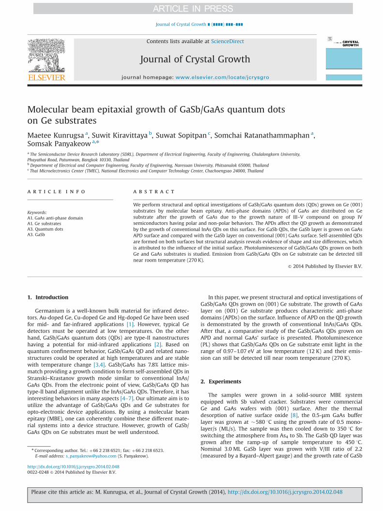
Fig. 1. (a) 5�5 μm2 AFM image of 0.5-μm GaAs grown on (001) Ge (001) substrate. (b) 5�5 μm2 AFM image of 1.8-ML InAs layer showing elongated self-assembled QDslocated near APD boundary. QDs are mainly located on the APD boundary. (c) Magnified image (2�2 μm2) of (b). The grayscale corresponds to the local surface slope.
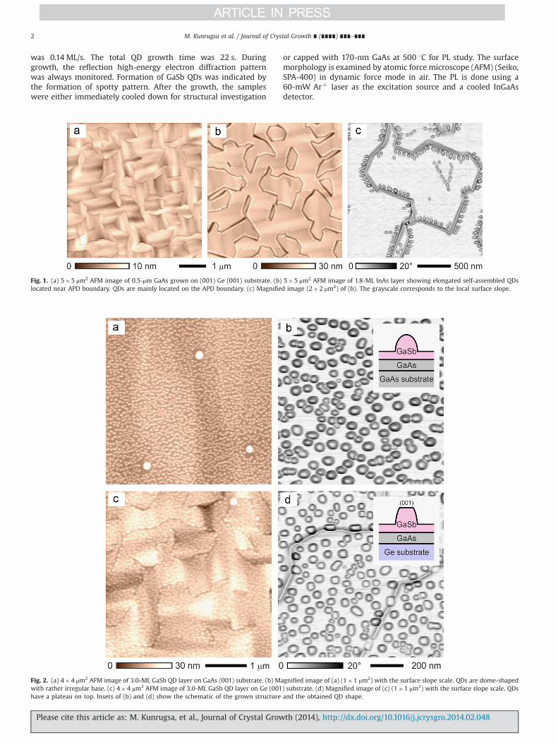
Fig. 2. (a) 4�4 μm2 AFM image of 3.0-ML GaSb QD layer on GaAs (001) substrate. (b) Magnified image of (a) (1�1 μm2) with the surface slope scale. QDs are dome-shapedwith rather irregular base. (c) 4�4 μm2 AFM image of 3.0-ML GaSb QD layer on Ge (001) substrate. (d) Magnified image of (c) (1�1 μm2) with the surface slope scale. QDshave a plateau on top. Insets of (b) and (d) show the schematic of the grown structure and the obtained QD shape.
M. Kunrugsa et al. / Journal of Crystal Growth ∎ (∎∎∎∎) ∎∎∎–∎∎∎2
Please cite this article as: M. Kunrugsa, et al., Journal of Crystal Growth (2014), http://dx.doi.org/10.1016/j.jcrysgro.2014.02.048i
3. Results and discussion
Epitaxial layer of GaAs could be grown on Ge substrates sinceGe and GaAs are mostly lattice-matched [9,10]. However, when apolar epitaxial layer of GaAs is grown on non-polar Ge substrates,APDs are typically formed. Fig. 1(a) shows a surface of 0.5-μm-thick GaAs grown on (001) Ge substrate. The surface is decoratedwith large APDs (in micron scale). Domain boundary is a kind ofdefect, which might affect the optical and electrical properties ofthe nanostructure grown on top. However, when the GaAs' APDsize is large compared to the size of QDs, the unique QD propertiesshould remain and be useful for device applications.
To demonstrate the influence of APD on QD growth, we grewconventional InAs QDs on the GaAs surface decorated with APDs[11]. Fig. 1(b) shows an AFM image of the InAs QDs on the surface.We found that InAs QDs are intensively located at the APDboundary. In addition, the QDs have an elongated shape with theirelongation being aligned with the grain boundary (Fig. 1(c)).According to the study of In(Ga)As QD shape on normal surface[12,13], the elongation of InAs QD shape is expected to be along½110� crystallographic direction. When the dot formation isobserved on one side of a particular domain wall, there will beno dots on the other side of the same domain wall. This indicationconfirms that the crystal orientation of each APD is perpendicularto that of its neighbor.
For a direct comparison, the GaSb QD growth on both (001) Geand (001) GaAs substrates was done at the same MBE growth run.Fig. 2 shows the AFM images of 3.0 ML GaSb/GaAs QDs on GaAssubstrate (Fig. 2(a) and (b)) and on Ge substrate (Fig. 2(c) and (d)).On the GaAs substrate, high density (�1.7�1010 cm�2) of GaSbQDs is observed on flat surface. Few large GaSb clusters, whichmay have originated from the Ostward ripening, are also seen.Magnified AFM image (Fig. 2(b) shows that the GaSb QDs aredome-shaped with rather irregular bases. Inset of Fig. 2(b) shows aschematic of the sample and QD structure.
For the GaSb QDs grown on GaAs APD on Ge substrate, the QDsare distributed on the entire surface of GaAs APDs even at thedomain boundary (Fig. 2(c)). The dots have large non-uniformityand they have no elongated shape as observed in the case of InAsQDs (Fig. 1(c)). From this result, we believe that the formation/relaxation mechanism of GaSb QDs on the APD surface is quitedifferent from that of InAs. In the case of GaSb, the APDs do notaffect the QD position, i.e., the QDs are densely formed everywhereon the surface. This effect can be due to the higher stickingcoefficient (and lower diffusibility) of Sb atoms [14,15]. The GaSbQDs might easily form on the surfaces due to the short diffusionlength of Ga and Sb atoms/molecules unlike InAs grown at thechosen rate and temperature [13]. This results in dense GaSb QDarray formed without having the influence of APDs on the QDposition.
On closely observing the shapes of GaSb QDs on GaAs' APDsurface, we found that mostQDs have (001) plateau on topwhile their base is rather non-uniform (Fig. 2(d) and its inset).Comparing with the dome-shaped GaSb QDs on GaAs substrate,we propose that the different QD shape is due to the difference instrain state. Presence of APD boundary in the initial surfacereduces the strain for GaSb material during the QD formation.Therefore, GaSb experiences lower mismatch and forms into adifferent QD shape. Shape-dependence on mismatch strain hasbeen observed in other materials [12,16].
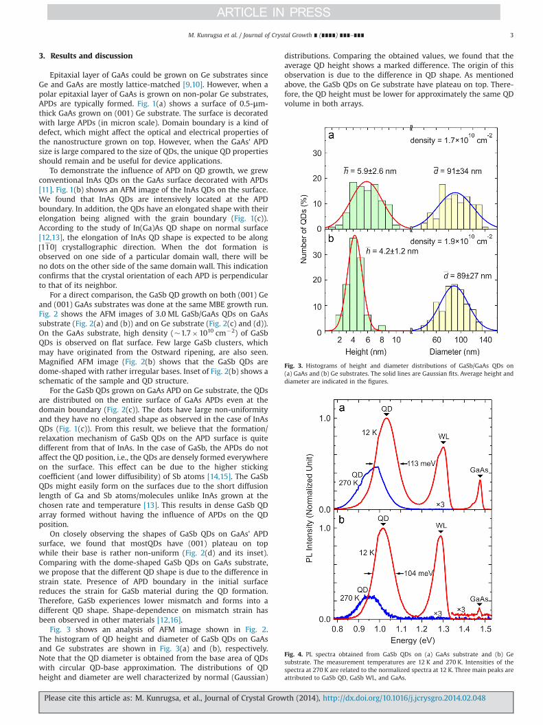
Fig. 3 shows an analysis of AFM image shown in Fig. 2.The histogram of QD height and diameter of GaSb QDs on GaAsand Ge substrates are shown in Fig. 3(a) and (b), respectively.Note that the QD diameter is obtained from the base area of QDswith circular QD-base approximation. The distributions of QDheight and diameter are well characterized by normal (Gaussian)
distributions. Comparing the obtained values, we found that theaverage QD height shows a marked difference. The origin of thisobservation is due to the difference in QD shape. As mentionedabove, the GaSb QDs on Ge substrate have plateau on top. There-fore, the QD height must be lower for approximately the same QDvolume in both arrays.
Fig. 3. Histograms of height and diameter distributions of GaSb/GaAs QDs on(a) GaAs and (b) Ge substrates. The solid lines are Gaussian fits. Average height anddiameter are indicated in the figures.
Fig. 4. PL spectra obtained from GaSb QDs on (a) GaAs substrate and (b) Gesubstrate. The measurement temperatures are 12 K and 270 K. Intensities of thespectra at 270 K are related to the normalized spectra at 12 K. Three main peaks areattributed to GaSb QD, GaSb WL, and GaAs.
M. Kunrugsa et al. / Journal of Crystal Growth ∎ (∎∎∎∎) ∎∎∎–∎∎∎ 3
Please cite this article as: M. Kunrugsa, et al., Journal of Crystal Growth (2014), http://dx.doi.org/10.1016/j.jcrysgro.2014.02.048i
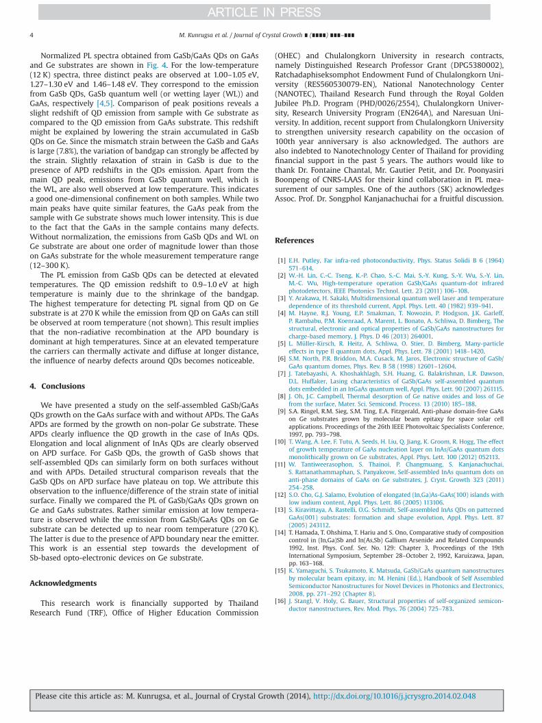
Normalized PL spectra obtained from GaSb/GaAs QDs on GaAsand Ge substrates are shown in Fig. 4. For the low-temperature(12 K) spectra, three distinct peaks are observed at 1.00–1.05 eV,1.27–1.30 eV and 1.46–1.48 eV. They correspond to the emissionfrom GaSb QDs, GaSb quantum well (or wetting layer (WL)) andGaAs, respectively [4,5]. Comparison of peak positions reveals aslight redshift of QD emission from sample with Ge substrate ascompared to the QD emission from GaAs substrate. This redshiftmight be explained by lowering the strain accumulated in GaSbQDs on Ge. Since the mismatch strain between the GaSb and GaAsis large (7.8%), the variation of bandgap can strongly be affected bythe strain. Slightly relaxation of strain in GaSb is due to thepresence of APD redshifts in the QDs emission. Apart from themain QD peak, emissions from GaSb quantum well, which isthe WL, are also well observed at low temperature. This indicatesa good one-dimensional confinement on both samples. While twomain peaks have quite similar features, the GaAs peak from thesample with Ge substrate shows much lower intensity. This is dueto the fact that the GaAs in the sample contains many defects.Without normalization, the emissions from GaSb QDs and WL onGe substrate are about one order of magnitude lower than thoseon GaAs substrate for the whole measurement temperature range(12–300 K).
The PL emission from GaSb QDs can be detected at elevatedtemperatures. The QD emission redshift to 0.9–1.0 eV at hightemperature is mainly due to the shrinkage of the bandgap.The highest temperature for detecting PL signal from QD on Gesubstrate is at 270 K while the emission from QD on GaAs can stillbe observed at room temperature (not shown). This result impliesthat the non-radiative recombination at the APD boundary isdominant at high temperatures. Since at an elevated temperaturethe carriers can thermally activate and diffuse at longer distance,the influence of nearby defects around QDs becomes noticeable.
4. Conclusions
We have presented a study on the self-assembled GaSb/GaAsQDs growth on the GaAs surface with and without APDs. The GaAsAPDs are formed by the growth on non-polar Ge substrate. TheseAPDs clearly influence the QD growth in the case of InAs QDs.Elongation and local alignment of InAs QDs are clearly observedon APD surface. For GaSb QDs, the growth of GaSb shows thatself-assembled QDs can similarly form on both surfaces withoutand with APDs. Detailed structural comparison reveals that theGaSb QDs on APD surface have plateau on top. We attribute thisobservation to the influence/difference of the strain state of initialsurface. Finally we compared the PL of GaSb/GaAs QDs grown onGe and GaAs substrates. Rather similar emission at low tempera-ture is observed while the emission from GaSb/GaAs QDs on Gesubstrate can be detected up to near room temperature (270 K).The latter is due to the presence of APD boundary near the emitter.This work is an essential step towards the development ofSb-based opto-electronic devices on Ge substrate.
Acknowledgments
This research work is financially supported by ThailandResearch Fund (TRF), Office of Higher Education Commission
(OHEC) and Chulalongkorn University in research contracts,namely Distinguished Research Professor Grant (DPG5380002),Ratchadaphiseksomphot Endowment Fund of Chulalongkorn Uni-versity (RES560530079-EN), National Nanotechnology Center(NANOTEC), Thailand Research Fund through the Royal GoldenJubilee Ph.D. Program (PHD/0026/2554), Chulalongkorn Univer-sity, Research University Program (EN264A), and Naresuan Uni-versity. In addition, recent support from Chulalongkorn Universityto strengthen university research capability on the occasion of100th year anniversary is also acknowledged. The authors arealso indebted to Nanotechnology Center of Thailand for providingfinancial support in the past 5 years. The authors would like tothank Dr. Fontaine Chantal, Mr. Gautier Petit, and Dr. PoonyasiriBoonpeng of CNRS-LAAS for their kind collaboration in PL mea-surement of our samples. One of the authors (SK) acknowledgesAssoc. Prof. Dr. Songphol Kanjanachuchai for a fruitful discussion.
References
[1] E.H. Putley, Far infra-red photoconductivity, Phys. Status Solidi B 6 (1964)571–614.
[2] W.-H. Lin, C.-C. Tseng, K.-P. Chao, S.-C. Mai, S.-Y. Kung, S.-Y. Wu, S.-Y. Lin,M.-C. Wu, High-temperature operation GaSb/GaAs quantum-dot infraredphotodetectors, IEEE Photonics Technol. Lett. 23 (2011) 106–108.
[3] Y. Arakawa, H. Sakaki, Multidimensional quantum well laser and temperaturedependence of its threshold current, Appl. Phys. Lett. 40 (1982) 939–941.
[4] M. Hayne, R.J. Young, E.P. Smakman, T. Nowozin, P. Hodgson, J.K. Garleff,P. Rambabu, P.M. Koenraad, A. Marent, L. Bonato, A. Schliwa, D. Bimberg, Thestructural, electronic and optical properties of GaSb/GaAs nanostructures forcharge-based memory, J. Phys. D 46 (2013) 264001.
[5] L. Müller-Kirsch, R. Heitz, A. Schliwa, O. Stier, D. Bimberg, Many-particleeffects in type II quantum dots, Appl. Phys. Lett. 78 (2001) 1418–1420.
[6] S.M. North, P.R. Briddon, M.A. Cusack, M. Jaros, Electronic structure of GaSb/GaAs quantum domes, Phys. Rev. B 58 (1998) 12601–12604.
[7] J. Tatebayashi, A. Khoshakhlagh, S.H. Huang, G. Balakrishnan, L.R. Dawson,D.L. Huffaker, Lasing characteristics of GaSb/GaAs self-assembled quantumdots embedded in an InGaAs quantumwell, Appl. Phys. Lett. 90 (2007) 261115.
[8] J. Oh, J.C. Campbell, Thermal desorption of Ge native oxides and loss of Gefrom the surface, Mater. Sci. Semicond. Process. 13 (2010) 185–188.
[9] S.A. Ringel, R.M. Sieg, S.M. Ting, E.A. Fitzgerald, Anti-phase domain-free GaAson Ge substrates grown by molecular beam epitaxy for space solar cellapplications. Proceedings of the 26th IEEE Photovoltaic Specialists Conference,1997, pp. 793–798.
[10] T. Wang, A. Lee, F. Tutu, A. Seeds, H. Liu, Q. Jiang, K. Groom, R. Hogg, The effectof growth temperature of GaAs nucleation layer on InAs/GaAs quantum dotsmonolithically grown on Ge substrates, Appl. Phys. Lett. 100 (2012) 052113.
[11] W. Tantiweerasophon, S. Thainoi, P. Changmuang, S. Kanjanachuchai,S. Rattanathammaphan, S. Panyakeow, Self-assembled InAs quantum dots onanti-phase domains of GaAs on Ge substrates, J. Cryst. Growth 323 (2011)254–258.
[12] S.O. Cho, G.J. Salamo, Evolution of elongated (In,Ga)As-GaAs(100) islands withlow indium content, Appl. Phys. Lett. 86 (2005) 113106.
[13] S. Kiravittaya, A. Rastelli, O.G. Schmidt, Self-assembled InAs QDs on patternedGaAs(001) substrates: formation and shape evolution, Appl. Phys. Lett. 87(2005) 243112.
[14] T. Hamada, T. Ohshima, T. Hariu and S. Ono, Comparative study of compositioncontrol in (In,Ga)Sb and In(As,Sb) Gallium Arsenide and Related Compounds1992, Inst. Phys. Conf. Ser. No. 129: Chapter 3, Proceedings of the 19thInternational Symposium, September 28–October 2, 1992, Karuizawa, Japan,pp. 163–168.
[15] K. Yamaguchi, S. Tsukamoto, K. Matsuda, GaSb/GaAs quantum nanostructuresby molecular beam epitaxy, in: M. Henini (Ed.), Handbook of Self AssembledSemiconductor Nanostructures for Novel Devices in Photonics and Electronics,2008, pp. 271–292 (Chapter 8).
[16] J. Stangl, V. Holy, G. Bauer, Structural properties of self-organized semicon-ductor nanostructures, Rev. Mod. Phys. 76 (2004) 725–783.
M. Kunrugsa et al. / Journal of Crystal Growth ∎ (∎∎∎∎) ∎∎∎–∎∎∎4
Please cite this article as: M. Kunrugsa, et al., Journal of Crystal Growth (2014), http://dx.doi.org/10.1016/j.jcrysgro.2014.02.048i