Modulo I- Conversion ADC-DAC
34
© 2009 Pearson Education, Upper Saddle River, NJ 07458. All Rights Reserved Floyd, Digital Fundamentals, 10 Digital Fundamentals Tenth Edition Floyd Chapter : ADC-DAC
description
precesamiento de señales
Transcript of Modulo I- Conversion ADC-DAC

© 2009 Pearson Education, Upper Saddle River, NJ 07458. All Rights Reserved Floyd, Digital Fundamentals, 10th ed
Digital Fundamentals
Tenth Edition
Floyd
Chapter : ADC-DAC

© 2009 Pearson Education, Upper Saddle River, NJ 07458. All Rights Reserved Floyd, Digital Fundamentals, 10th ed
Summary
Most input signals to an electronic system start out as analog signals. For processing, the signal is normally converted to a digital signal by sampling the input.
Sampling
Samplingcircuit
Sampledversion of
input signal
Analoginput
signal
Samplingpulses
Before sampling, the analog input must be filtered with a low-pass anti-aliasing filter. The filter eliminates frequencies that exceed a certain limit that is determined by the sampling rate.

© 2009 Pearson Education, Upper Saddle River, NJ 07458. All Rights Reserved Floyd, Digital Fundamentals, 10th ed
Summary
To understand the need for an anti-aliasing filter, you need to understand the sampling theorem which essentially states:
Anti-aliasing Filter
where fsample = sampling frequency fa(max) = highest harmonic in the analog signal
Stated as an equation, fsample > 2fa(max)
In order to recover a signal, the sampling rate must be greater than twice the highest frequency in the signal.
If the signal is sampled less than this, the recovery process will produce frequencies that are entirely different than in the original signal. These “masquerading” signals are called aliases.

© 2009 Pearson Education, Upper Saddle River, NJ 07458. All Rights Reserved Floyd, Digital Fundamentals, 10th ed
Summary
The anti-aliasing filter is a low-pass filter that limits high frequencies in the input signal to only those that meet the requirements of the sampling theorem.
Anti-aliasing Filter
Unfiltered analog frequency spectrum
Overlap causes aliasing error
fc
Filtered analog frequency spectrum
f fsample
Sampling frequency spectrum
The filter’s cutoff frequency, fc, should be less than ½ fsample.

© 2009 Pearson Education, Upper Saddle River, NJ 07458. All Rights Reserved Floyd, Digital Fundamentals, 10th ed
To process naturally occurring analog quantities with a digital system, the analog signal is converted to digital form after the anti-aliasing filter.
Summary
Analog-to-Digital Conversion
The first step in converting a signal to digital form is to use a sample-and-hold circuit. This circuit samples the input signal at a rate determined by a clock signal and holds the level on a capacitor until the next clock pulse. A positive half-wave from 0-10 V is shown in blue. The sample-and-hold circuit produces the staircase representation shown in red.
0 V
10 V

© 2009 Pearson Education, Upper Saddle River, NJ 07458. All Rights Reserved Floyd, Digital Fundamentals, 10th ed
Summary
The second step is to quantize these staircase levels to binary coded form using an analog-to-digital converter (ADC). The digital values can then be processed by a digital signal processor or computer.
0.000010.0001100.0001101.1110111.01111000.10111001.10011010.00001010.00001001.10011000.1011111.0111101.1110100.000110.00010.00000 V
10 V
What is the maximum unsigned binary value for the waveform?
10 V = 10102 V. The table lists the quantized binary values for all of the steps. Peak = 10 V
Analog-to-Digital Conversion

© 2009 Pearson Education, Upper Saddle River, NJ 07458. All Rights Reserved Floyd, Digital Fundamentals, 10th ed
Summary
Most signals have higher frequency harmonic and noise. For most ADCs, the sampling and filter cutoff frequencies are selected to be able to reconstruct the desired signal without including unnecessary harmonics and noise.
Anti-aliasing Filter
An example of a reasonable sampling rate is in a digital audio CD. For audio CDs, sampling is done at 44.1 kHz because audio frequencies above 20 kHz are not detectable by the ear.
What cutoff frequency should an anti-aliasing filter have for a digital audio CD?
Less than 22.05 kHz.

© 2009 Pearson Education, Upper Saddle River, NJ 07458. All Rights Reserved Floyd, Digital Fundamentals, 10th ed
Summary
Sample-and-Hold and ADC
Following the anti-aliasing filter, is the sample-and-hold circuit and the analog-to-digital converter. At this point, the original analog signal has been converted to a digital signal.
Many ICs can perform both functions on a single chip and include two or more channels. For audio applications, the AD1871 is an example of a stereo audio ADC.
Samples held for one clock pulse
. . . . . . .ADC . . . .
. . . . .
0 1 0 0 0 1 0 1 1 1 0 0 1 0 1 0

© 2009 Pearson Education, Upper Saddle River, NJ 07458. All Rights Reserved Floyd, Digital Fundamentals, 10th ed
R
R
R
R
R
R
R
R
Op-ampcomparators
Priorityencoder
D0D1
D2
Parallelbinaryoutput
Enablepulses
Input fromsample-
and-hold
+VREF
–+
–+
–+
–+
–+
–+
–+
76543210 EN
421
Summary
Analog-to-Digital Conversion Methods
The flash ADC: The flash ADC uses a series high-speed comparators that compare the input with reference voltages. Flash ADCs are fast but require 2n – 1 comparators to convert an analog input to an n-bit binary number.
How many comparators are needed by a 10-bit flash ADC?
1023

© 2009 Pearson Education, Upper Saddle River, NJ 07458. All Rights Reserved Floyd, Digital Fundamentals, 10th ed
Summary
Analog-to-Digital Conversion Methods
The dual-slope ADC: 1. The dual-slope ADC integrates the input voltage for a fixed time while the counter counts to n. 2. Control logic switches to the VREF input.
–
+
CLK
Controllogic
C
Latches
EN
D7 D6 D5 D4 D3 D2 D1 D0
R
–
+
Vin
–VREF
SWR
C
A 1 A2≈0 V
–+
n
Counter
SW -V
–V
0t = n counts
Fixed interval
Variablevoltage
Variableslope
I
HIGH HIGH
I
–V
0
Variable time
Fixed-sloperamp
2. A fixed-slope ramp starts from –V as the counter counts. When it reaches 0 V, the counter output is latched.
© 2009 Pearson Education, Upper Saddle River, NJ 07458. All Rights Reserved Floyd, Digital Fundamentals, 10th ed
Summary
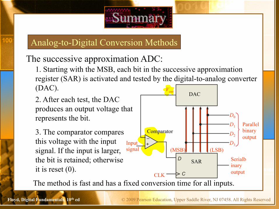
Analog-to-Digital Conversion Methods
The successive approximation ADC: 1. Starting with the MSB, each bit in the successive approximation register (SAR) is activated and tested by the digital-to-analog converter (DAC). 2. After each test, the DAC produces an output voltage that represents the bit.
3. The comparator compares this voltage with the input signal. If the input is larger, the bit is retained; otherwise it is reset (0).
D
–+
C
SAR
DAC Vout
Parallel binary output
CLK
D0
D1
D2
D3
Serialbinary output
Input signal
Comparator
(MSB) (LSB)
The method is fast and has a fixed conversion time for all inputs.

© 2009 Pearson Education, Upper Saddle River, NJ 07458. All Rights Reserved Floyd, Digital Fundamentals, 10th ed
Summary
Analog-to-Digital Conversion Methods
An integrated circuit successive approximation ADC is the ADC804. This popular ADC is an 8-bit converter that completes a conversion in 64 clock periods (100 µs).
VCC
Digitaldataoutput
INTR(5)
D7(11) D6(12) D5(13) D4(14) D3(15) D2(16) D1(17) D0(18) CLK R (out)(19)
(8)
ANLGGND
(10)
CS(1)
REF/2(9)Vin–(7)Vin+(6)CLK IN(4)(3)(2)
RDWR
Analoginput
DGTLGND
(20)
ADC0804
∆∆∆∆∆∆∆∆
The completion is signaled by the INTR line going LOW.

© 2009 Pearson Education, Upper Saddle River, NJ 07458. All Rights Reserved Floyd, Digital Fundamentals, 10th ed
Summary
Analog-to-Digital Conversion Methods
The sigma-delta ADC: With sigma-delta conversion, the difference between two samples of the analog input signal integrated and quantized. The density of 1s at the output is proportional to the input signal.
1-bitquantizerIntegratorΣ
+Analoginput
signal
DAC
–
Quantized outputis a single bitdata stream.
∆
Summingpoint
© 2009 Pearson Education, Upper Saddle River, NJ 07458. All Rights Reserved Floyd, Digital Fundamentals, 10th ed
Summary
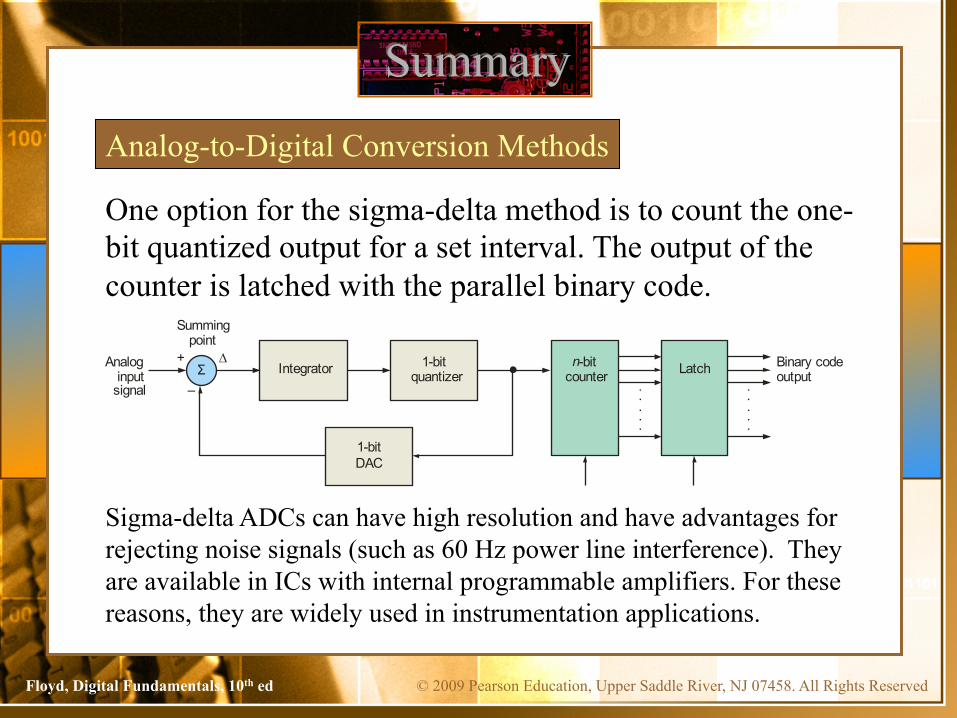
Analog-to-Digital Conversion Methods
One option for the sigma-delta method is to count the one-bit quantized output for a set interval. The output of the counter is latched with the parallel binary code.
Sigma-delta ADCs can have high resolution and have advantages for rejecting noise signals (such as 60 Hz power line interference). They are available in ICs with internal programmable amplifiers. For these reasons, they are widely used in instrumentation applications.
.
.
.
.
.
.
.
.
.
.
1-bitquantizerIntegratorΣ
+Analoginput
signal
1-bitDAC
–
∆ n-bitcounter Latch Binary code
output
Summingpoint
© 2009 Pearson Education, Upper Saddle River, NJ 07458. All Rights Reserved Floyd, Digital Fundamentals, 10th ed
Summary
Digital-to-Analog Conversion Methods
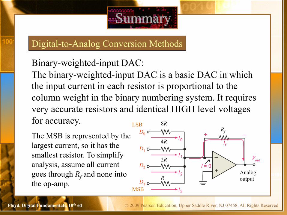
Binary-weighted-input DAC: The binary-weighted-input DAC is a basic DAC in which the input current in each resistor is proportional to the column weight in the binary numbering system. It requires very accurate resistors and identical HIGH level voltages for accuracy. The MSB is represented by the largest current, so it has the smallest resistor. To simplify analysis, assume all current goes through Rf and none into the op-amp.
MSB
LSB
–
+
I0
I = 0
I1
I2
I3
If
+ –
8R
4R
2R
R
Rf
Vout
Analog output
D0
D1
D2
D3

© 2009 Pearson Education, Upper Saddle River, NJ 07458. All Rights Reserved Floyd, Digital Fundamentals, 10th ed
–
+
Summary
Digital-to-Analog Conversion Methods
A certain binary-weighted-input DAC has a binary input of 1101. If a HIGH = +3.0 V and a LOW = 0 V, what is Vout?
+3.0 V
+3.0 V
+3.0 V
0 V
120 kΩ
60 kΩ
30 kΩ
15 kΩ
10 kΩ
Rf
0 1 2 3( )3.0 V 3.0 V 3.0 V0 V 0.325 mA
120 k 30 k 15 k
outI I I I I= − + + +
⎛ ⎞= − + + + = −⎜ ⎟Ω Ω Ω⎝ ⎠
Vout = Iout Rf = (−0.325 mA)(10 kΩ) = −3.25 V
Vout

© 2009 Pearson Education, Upper Saddle River, NJ 07458. All Rights Reserved Floyd, Digital Fundamentals, 10th ed
–
+
Summary
Digital-to-Analog Conversion Methods R-2R ladder: The R-2R ladder requires only two values of resistors. By calculating a Thevenin equivalent circuit for each input, you can show that the output is proportional to the binary weight of inputs that are HIGH.
2R R R R
2R 2R 2R 2R Rf = 2R
Inputs D0 D1 D2 D3
Each input that is HIGH contributes to the output: 2S
out n i
VV−
= −
Vout
where VS = input HIGH level voltage n = number of bits i = bit number
R1 R3 R5 R7
R2 R4 R6 R8
For accuracy, the resistors must be precise ratios, which is easily done in integrated circuits.
© 2009 Pearson Education, Upper Saddle River, NJ 07458. All Rights Reserved Floyd, Digital Fundamentals, 10th ed
Summary
Digital-to-Analog Conversion Methods
Rf = 50 kΩ
0 V +5.0 V
Vout
R1 R3 R5 R7
R2 R4 R6 R8
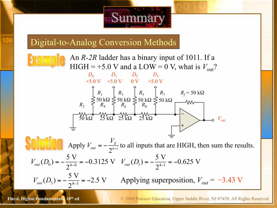
An R-2R ladder has a binary input of 1011. If a HIGH = +5.0 V and a LOW = 0 V, what is Vout?
50 kΩ
25 kΩ
50 kΩ 50 kΩ 50 kΩ
50 kΩ 25 kΩ 25 kΩ
+5.0 V +5.0 V
0 4 0
5 V( ) 0.3125 V2outV D
−= − = − 1 4 1
5 V( ) 0.625 V2outV D
−= − = −
3 4 3
5 V( ) 2.5 V2outV D
−= − = −
–
+
D0 D1 D2 D3
Applying superposition, Vout = −3.43 V
2S
out n i
VV−
= −Apply to all inputs that are HIGH, then sum the results.

© 2009 Pearson Education, Upper Saddle River, NJ 07458. All Rights Reserved Floyd, Digital Fundamentals, 10th ed
Summary
Resolution and Accuracy of DACs
The R-2R ladder is relatively easy to manufacturer and is available in IC packages. DACs based on the R-2R network are available in 8, 10, and 12-bit versions. The resolution is an important specification, defined as the reciprocal of the number of steps in the output.
What is the resolution of the BCN31 R-2R ladder network, which has 8-bits?
28 – 1 = 255 1/255 = 0.39%
The accuracy is another important specification and is derived from a comparison of the actual output to the expected output. For the BCN31, the accuracy is specified as ±½ LSB = 0.2%.

© 2009 Pearson Education, Upper Saddle River, NJ 07458. All Rights Reserved Floyd, Digital Fundamentals, 10th ed
Summary
Reconstruction Filter
Reconstruction Filter
Output of the DAC Final analog output
After converting a digital signal to analog, it is passed through a low-pass “reconstruction filter” to smooth the stair steps in the output. The cutoff frequency of the reconstruction filter is often set to the same limit as the anti-aliasing filter, to block higher harmonics due to the digitizing process.
© 2009 Pearson Education, Upper Saddle River, NJ 07458. All Rights Reserved Floyd, Digital Fundamentals, 10th ed
Summary
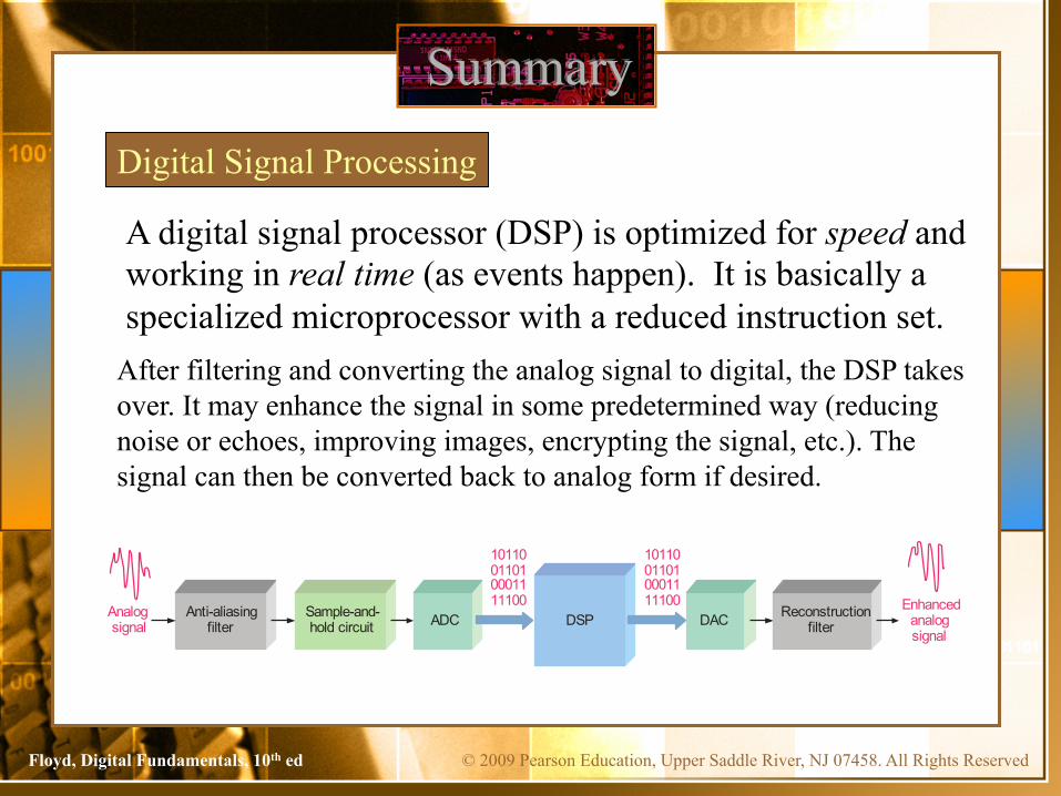
A digital signal processor (DSP) is optimized for speed and working in real time (as events happen). It is basically a specialized microprocessor with a reduced instruction set.
Digital Signal Processing
Analogsignal ADC DSP DAC Reconstruction
filterSample-and-hold circuit
Anti-aliasingfilter
Enhancedanalogsignal
10110011010001111100
10110011010001111100
After filtering and converting the analog signal to digital, the DSP takes over. It may enhance the signal in some predetermined way (reducing noise or echoes, improving images, encrypting the signal, etc.). The signal can then be converted back to analog form if desired.

© 2009 Pearson Education, Upper Saddle River, NJ 07458. All Rights Reserved Floyd, Digital Fundamentals, 10th ed
Summary
Because speed is important in DSP applications, assembly language is frequently used because in general it executes faster.
Digital Signal Processing
Program cache/program memory(32-bit address, 256-bit data)
Register file A
Data path A
Instruction decode
Register file B
Data path B
Instruction dispatch
Program fetchControlregisters
Controllogic
Test
Evaluation
Interrupts
CPU (DSP core)
Additionalperipherals
Data cache/data memory(32-bit address, 8-, 16-, 32-. 64-bit data)
DMAEMIF
.S1 .M1 .D1.L1 .M2 .S2 .L2.D2
A general block diagram of the TMS320C6000 series DSP

© 2009 Pearson Education, Upper Saddle River, NJ 07458. All Rights Reserved Floyd, Digital Fundamentals, 10th ed
Selected Key Terms
Nyquist frequency
Quantization
���Analog-to-digital converter (ADC)
DSP
Digital-to-analog converter (DAC)
The highest signal frequency that can be sampled at a specified sampling frequency; a frequency equal or less than half the sampling frequency.
The process whereby a binary code is assigned to each sampled value during analog-to-digital conversion.
A circuit used to convert an analog signal to digital form.
Digital signal Processor; a special type of microprocessor that processes data in real time.
A circuit used to convert a digital signal to analog form.

© 2009 Pearson Education, Upper Saddle River, NJ 07458. All Rights Reserved Floyd, Digital Fundamentals, 10th ed
1. If an anti-aliasing filter is not used in digitizing a signal the recovery process
a. is slowed
b. may include alias signals
c. will have less noise
d. all of the above
© 2008 Pearson Education

© 2009 Pearson Education, Upper Saddle River, NJ 07458. All Rights Reserved Floyd, Digital Fundamentals, 10th ed
2. An anti-aliasing filter should have
a. fc more than 2 times the Nyquist frequency
b. fc equal to the Nyquist frequency
c. fc more than ½ fsample
d. fc less than ½ fsample
© 2008 Pearson Education

© 2009 Pearson Education, Upper Saddle River, NJ 07458. All Rights Reserved Floyd, Digital Fundamentals, 10th ed
3. The number of comparators required in a 10-bit flash ADC is
a. 255
b. 511
c. 1023
d. 4095
© 2008 Pearson Education

© 2009 Pearson Education, Upper Saddle River, NJ 07458. All Rights Reserved Floyd, Digital Fundamentals, 10th ed
4. The block diagram is for a successive-approximation ADC. The top block is
a. an SAR
b. a DAC
c. an ADC
d. a comparator
© 2008 Pearson Education
D
–+
C
Vout
CLK
D0
D1
D2
D3
Serialbinary output
Input signal (MSB) (LSB)
Parallel binary output

© 2009 Pearson Education, Upper Saddle River, NJ 07458. All Rights Reserved Floyd, Digital Fundamentals, 10th ed
5. The ADC804 integrated circuit signals a completed conversion by
a. INTR goes LOW
b. CS goes LOW
c. RD goes LOW
d. CLK R goes HIGH
© 2008 Pearson Education
VCC
Digitaldataoutput
INTR(5)
D7(11) D6(12) D5(13) D4(14) D3(15) D2(16) D1(17) D0(18) CLK R (out)(19)
(8)
ANLGGND
(10)
CS(1)
REF/2(9)Vin–(7)Vin+(6)CLK IN(4)(3)(2)
RDWR
Analoginput
DGTLGND
(20)
ADC0804
∆∆∆∆∆∆∆∆

© 2009 Pearson Education, Upper Saddle River, NJ 07458. All Rights Reserved Floyd, Digital Fundamentals, 10th ed
6. A sigma-delta circuit is a form of
a. DSP
b. DAC
c. ADC
d. SAR
© 2008 Pearson Education

© 2009 Pearson Education, Upper Saddle River, NJ 07458. All Rights Reserved Floyd, Digital Fundamentals, 10th ed
7. The circuit shown is a
a. DSP
b. DAC
c. ADC
d. SAR
© 2008 Pearson Education
–
+
I0
I = 0
I1
I2
I3
If
+ –
8R
4R
2R
R
Rf
Vout

© 2009 Pearson Education, Upper Saddle River, NJ 07458. All Rights Reserved Floyd, Digital Fundamentals, 10th ed
8. For the circuit shown, the input on the far left is for the
a. analog input
b. clock
c. LSB
d. MSB
© 2008 Pearson Education
–
+2R R R R
2R 2R 2R 2R Rf = 2R
Inputs
Vout
R1 R3 R5 R7
R2 R4 R6 R8

© 2009 Pearson Education, Upper Saddle River, NJ 07458. All Rights Reserved Floyd, Digital Fundamentals, 10th ed
9. A reconstruction filter
a. is a low-pass filter
b. can have the same response as an anti-aliasing filter
c. smoothes the output from a DAC
d. all of the above
© 2008 Pearson Education

© 2009 Pearson Education, Upper Saddle River, NJ 07458. All Rights Reserved Floyd, Digital Fundamentals, 10th ed
10. A DSP is a specialized microprocessor that
a. has a very large instruction set
b. is deigned to be very fast
c. has internal anti-aliasing and reconstruction filters
d. all of the above
© 2008 Pearson Education
© 2009 Pearson Education, Upper Saddle River, NJ 07458. All Rights Reserved Floyd, Digital Fundamentals, 10th ed
Answers:
1. b
2. d
3. c
4. b
5. a
6. c
7. b
8. c
9. d
10. b