Module Size: 12.02 inch 2160RGBx1440 Spec Part No ...
34
LCD MODULE SPECIFICATION Module Size: 12.02 inch 2160RGBx1440 Spec Part No.: 23040475 Date : 2016-03-11 Version : 2.2
Transcript of Module Size: 12.02 inch 2160RGBx1440 Spec Part No ...

LCD MODULE
SPECIFICATION
Module Size: 12.02 inch 2160RGBx1440
Spec Part No.: 23040475
Date : 2016-03-11
Version : 2.2

Revision History
Version Revise Date Page Content Prepared by
1.0 2015-07-21 ALL First release Xushuang
2.0 2015-08-10
P4, P5,
P6, P11,
P12,P13,
P26, P28
P4 Revise Module Size
P5 Revise Active Area, Gamma Correction,
and Gate scan direction.
P6~P7 Revise Pin symbol and Pin 28
definition.
P11 Revise Power consumption of Panel
P12 Revise power consumption of backlight
and add Note6.
P13 Revise requirement of color coordinate
P26 Revise Mechanical Drawing
P28 Add remarks on items of Extrusion and
Ball Drop Test.
Xushuang
2.1 2015-09-18
P5,
P6,P7,P8
,P12,P13
,P14,P15
,P16,P18
,P20,
P27,P28
P5 Revise module weight,dynamic contrast
and gamma correction.
P5、P6 Revise warpage test item
P7、P8 Revise Pin 28 definition and add
voltage item.
Revise HSYNC、HPD、DBC_EN、
BL_PWM_IN、BL_PWM_OUT voltage.
P12 Revise LED PWM_OUT voltage.
P13 Revise Note5.
P14 Revise color uniformity and color
coordinate.
P15 Revise Note7.
P16 Revise Note8.
P18 Revise Note12.
P20 Revise note 15
P27 Revise Mechanical Drawing
P28 Revise LDI 3point bending test item
Liulifeng
2.2 2016-03-11 P15
P28
P15 Revise Color Uniformity:
From △u’△ v’-A:max0.012,△u’△
v’-B:max0.004 to
△u’△ v’-A:max0.015,△u’△ v’-B:
max0.005
P15 Revise Color coordinate:From
R(0.6509,0.3302),G(0.2708,0.6632)
to
R(0.6609,0.3302),G(0.2738,0.6432)
P28 Revise Mechanical Drawing
Liulifeng

Table of Contents
1 General Specification .............................................................................................................. 4
1.1 Features ........................................................................................................................ 4
2 LCM Specification .................................................................................................................. 4
2.1 Application ................................................................................................................... 4
2.2 General Specification .................................................................................................. 4
3 Pin Assignments....................................................................................................................... 7
3.1 Display Interface ......................................................................................................... 7
4 Schematic Circuit Diagram .................................................................................................... 9
4.1 Display Edp1.3 Reference Circuit .............................................................................. 9
5 Register &Pixel Data Format ................................................................................................. 9
5.1 eDP1.3 Data Format.................................................................................................... 9
6 Timing Characteristics ......................................................................................................... 10
6.1 Power on / off Sequence ............................................................................................ 10
6.2 eDP1.3 Interface Characteristics ............................................................................. 11
7 Electrical Specifications ........................................................................................................ 12
7.1 LCD Typical Operation Conditions ........................................................................ 12
7.2 Power Consumption of TFT Panel .......................................................................... 12
7.3 Power Consumption of Backlight ............................................................................ 12
8 Optical Specifications ........................................................................................................... 13
9 Mechanical Drawing ............................................................................................................. 26
10 Reliability Requirement ........................................................................................................ 27
10.1 General Reliability Requirement ............................................................................. 27
10.2 Incoming Inspection Requirement .......................................................................... 33
10.3 Module Unit Reliability Test .................................................................................... 33

1 General Specification
1.1 Features
1.1.1 LCM Features
-- TFT-LCD Panel with IPS type
-- 2160RGBx1440 Resolution
--Interface eDP 1.3 with PSR
--NTSC 85%
--One backlight with 54pcs RG LED
-- Landscape LCD
2 LCM Specification
2.1 Application
Display module for Portable Terminal
2.2 General Specification
No. Item Specification Unit Remark
1 Display Size 12.02 Inch
2 TFT Technology
Type
a-Si
3 Liquid Crystal
Alignment Method
IPS or equivalence
4 Resolution 2160*RGB*1440
5 Display mode Transmissive
6 Color Depth 16.7M(RGB 24bit)
7 Viewing Direction Full Viewing Angle
Min75/Typ80@CR>10
8 Contrast Ratio 800 min/1000 typ
9 Luminance 380 min/450 typ cd/m2 9point average
10 Module Size LCM 262.42 (W)*179.55(H)*Max2.25 (T) mm Note 1
CPK>1.33
11 Thickness Panel:0.2(Typ)/0.2(Typ) mm Note 1
Module: Max4.25 (w PCBA)
12 Panel Active Area 254.016(W)*169.344(H) mm Note 1
13 Pixel Size 0.0392(W)*0. 1176(H) mm
14 Pixel Pitch 0.1176(W)×0.1176(H) mm
15 Pixel Aspect Ratio 1:1
16 Driver IC TBD
17 Light Source RG LED Backlight
18 Interface eDP1.3
19 Vcom type DC Vcom
20 Driver Inversion
type
column Inversion or Z Inversion
21 Operation
Temperature
-10~+60 degC
22 Storage Temperature -20~+70 degC
23 Weight 168g(max) Gram
24 Pixel Per inch 216 PPI
25 Pixel Aperture Ratio TBD %
26 Environmental
Protection
Requirement
RoHS & REACH must be executed
27 Connection method ZIF 40Pins
28 PSR(RAM Size) Need
29 Color Enhancement Need Note 4
30 CABC Function Need
31 E-EDID Implementing an EDID 1.3 or later data
structure
32 Dynamic Contrast Need
33 Gamma Correction Need
34 Polarizer Type Hard coat treating 3H
Glare
35 Panel gate scan
direction reverse
TBD
36 warpage front side value < 0.4mm
rear side value < 0.4mm.
Note 2,
And refer to 1st lot
37 Diagonal
Stripes&Morie
Invisible Note 3
38 MBO Function Need
Note 1:Please Refer to the mechanical drawing.
Note 2: Warpage inspected by measuring system to analyze surface warpage and module
thickness.
[1] Tp side test

• Remove protect film of TP side,put glass face down on the marble platform as
shown in the figure.
• Smooth around bezel tape in order to prevent the bubble impact test.
• Test the warpage of TP side with feeler guage in order of 1,2,3,4,5,6,7,8.
[2] LCD side test
• Remove protect film of both side,put backlight face down on the marble platform as
shown in the figure.

• Smooth around bezel tape in order to prevent the bubble impact test.
• Test the warpage of LCD side with feeler guage in order of 1,2,3,4,5,6,7.
Note 3: Viewing distance: 20cm to 25cm.
Viewing angle: θL <45° , θR <45° , ψT<45°, ψB<45° .
The viewing angle Refer to Note 9.
Note 4: The detail test method can refer to the template of HUAWEI Display Validation test
report.
3 Pin Assignments
3.1 Display Interface
Pin No. Symbol Voltage Description I/O
1 VCCS 3.3V LCD logic and driver power P
2 VCCS 3.3V LCD logic and driver power P
3 VCCS 3.3V LCD logic and driver power P
4 HSYNC 3.3V Horizontal SYNC signal O
5 ID 3.3V/0V ID Pin -
6 BIST NA BIST enable I
7 GND Ground P
8 AUX_CH_N 500mV(min) Complement Signal Auxiliary
Channel I/O
9 AUX_CH_P 1000mV (max) True Signal Auxiliary Channel I/O
10 GND Ground P
11 Lane0_N 100mV(min) Complement Signal Link Lane 0 I
12 Lane0_P 1320mV (max) True Signal Link Lane 0 I
13 GND Ground P
14 Lane1_N 100mV(min) Complement Signal Link Lane 1 I
15 Lane1_P 1320mV (max) True Signal Link Lane 1 I
16 GND Ground P
17 Lane2_N 100mV(min) Complement Signal Link Lane 2 I
18 Lane2_P 1320mV (max) True Signal Link Lane 2 I
19 GND Ground P
20 Lane3_N 100mV(min) Complement Signal Link Lane 3 I
21 Lane3_P 1320mV (max) True Signal Link Lane 3 I

22 GND Ground P
23 HPD 3.3V HPD signal pin I/O
24 GND Ground P
25 WPN NA I2C Write Protection I
26 SCL NA I2C CLK I
27 SDA NA I2C SDA I/O
28 DBC_EN 3.3V/0V Pull High Enable, Pull Low
Disable I
29 BL_PWM_IN 3.3V System PWM signal input for
dimming I
30 BL_PWM_OUT 3.3V Bypass PWMI or
TCON output PWM for BL control O
31 LED_1 Power for LED1 Cathode P
32 LED_2 Power for LED2 Cathode P
33 LED_3 Power for LED3 Cathode P
34 LED_4 Power for LED4 Cathode P
35 LED_5 Power for LED5 Cathode P
36 LED_6 Power for LED6 Cathode P
37 NC Reserved for LCD manufacturer’s
use -
38 BL_VCCS 29V Power for LED Anode P
39 BL_VCCS 29V Power for LED Anode P
40 BL_VCCS 29V Power for LED Anode P

4 Schematic Circuit Diagram
4.1 Display Edp1.3 Reference Circuit
5 Register &Pixel Data Format
5.1 eDP1.3 Data Format

6 Timing Characteristics
6.1 Power on / off Sequence

6.2 eDP1.3 Interface Characteristics
support for Panel Self Refresh (PSR)
7 Electrical Specifications
7.1 LCD Typical Operation Conditions
Item Symbol Values Unit
Remark
Min Typ Max
Power Supply Voltage VCCS 3.0 3.3 3.6 V
Ripple Voltage VRP - (50) - mV
LED
PWM OUT
High Level VOH 3.0 3.3 3.6 V
Low Level VOL - - 0.495 V
Frame frequency fFrame - 60 - HZ
Hot plug Detect HPD - 3.3 - V
7.2 Power Consumption of TFT Panel
Power Supply: Frame Frequency: Fframe =60HZ @ 25degC456
Display Mode Item Symbol Value Unit Remark
Typ Max
Display White Current of VCCS I VCCS TBD 348 mA
Display Black Current of VCCS I VCCS TBD TBD mA
Standby Mode Current of VCCS I VCCS TBD TBD mA
Worst pattern Current of VCCS I VCCS TBD TBD mA
7.3 Power Consumption of Backlight
Test Condition : ILED=21mA RG LED 54PCS
Warning: LCM Brightness must match Optical Spec requirement when ILED=21mA
Backlight Unit Schematic:

Item Symbol Value Unit Remark
Min Typ Max
Forward
Voltage
VBL TBD 28.8 V Note 5
Power
Consumption
PBL TBD 3650 mW
LED Quantity 54 pcs
LED Rank
Luminous Flux: TBD lm
Chromaticity:TBD
Note 5 : When ILED=21mA,the VBL must be in the range of above table specified.
The FPC wire resistance between LED+ and LED- must be less than
0.15ohm
PBL= ILEDX VBL
Note 6 : The overall Power consumption of Backlight and Panel is less than 4600mW.
8 Optical Specifications
Test condition:VCCS =3.3V ,Ta=25℃
Item Symbol Condition Value
Unit Note Min Typ Max
luminance Bp θ=0°
=0°
380 450 -- cd/m2 Note 7
Uniformity △Bp 75 80 -- % Note 8
Color Uniformity △u’△ v’-A -- -- 0.015 Note 26

△u’△ v’-B -- -- 0.005 Sign the limit
sample shall
prevail.
△E*ab -- -- NA
Viewing
Angle
Left θL
Cr≥10
75 80 --
deg Note 9
Right θR 75 80 --
Top ψT 75 80 --
Bottom ψB 75 80 --
Contrast Ratio Cr
θ=0°
=0°
800 1000 -- - Note 10
Response
Time
Tr+Tf -- 25 35
m
s Note 11
Tgray - 45 55 ms
Color
Coordinat
e of
CIE1931
Red x
θ=0°
=0°
Typ-0.03 0.6609 Typ+0.03
-
Note 12
y Typ-0.03 0.3302 Typ+0.03
Green x Typ-0.03 0.2738 Typ+0.03
y Typ-0.03 0.6432 Typ+0.03
Blue x Typ-0.03 0.1497 Typ+0.03
y Typ-0.03 0.0600 Typ+0.03
White x 0.27 0.30 0.33
y 0.28 0.31 0.34
NTSC Ratio NTSC CIE1931 -- 85 -- % Note 13
Color Temperature CT - 7500 -
Flicker amoun
t - - - -30 dB Note 14
Gamma - 1.9 2.2 2.5 Note 15
Crosstalk △CT - - 1.10 1.20 Note 16
Transmittance
@w/o APF Tm TBD -- %
Reflectance Rf @550nm -- TBD % Note 17
Polarization
Direction of Front
Polarizer
TBD deg
Note 18
Polarization
Direction of Rear
Polarizer
PdR TBD deg
Luminance
decrease ratio
θL=30° --- --- 70 %
Note 19
θR=30° --- --- 70 %
ψT=30° --- --- 70 %
ψB=30° --- --- 70 %
Contrast
decrease ratio
θL=30° --- --- 70 %
Note 20
θR=30° --- --- 70 %
ψT=30° --- --- 70 %
ψB=30° --- --- 70 %

Color shift
θL=30° --- --- 3 JNCD
Note 21
θR=30° --- --- 3 JNCD
ψT=30° --- --- 3 JNCD
ψB=30° --- --- 3 JNCD
Gray inversion angle ψ=0° NA deg Note 22
Sunglass Readability NA
Afterimage 3 Minute Note 23
CABC Test Note 24
Hot spot △Bp
θ=0°
=0° 75 80 % Note25
θ=0°
=0° 80 85 %
Every near 9
points Note25
Note 7: Luminance measurement
The test condition is at ILED=21mA and measured on the surface of LCD module at 25℃.
• The data are measured after LEDs are lighted on for more than 5 minutes and LCM
displays are fully white. The brightness is the average value of 9 measured spots.
Measurement equipment CS2000 or similar equipments (Field of
view:1deg,Distance:50cm)
• Measuring surroundings: Dark room.
• Measuring temperature: Ta=25℃.
• Adjust operating voltage to get optimum contrast at the center of the display.
• Measured value at the center point of LCD panel must be after more than 5 minutes
while backlight turning on.
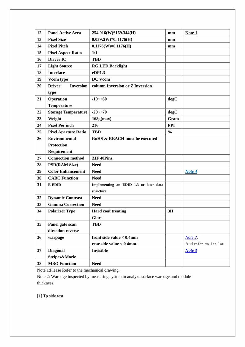
Note 8: Uniformity
• The test condition is at ILED=21mA and measured on the surface of LCD module at
25℃.
• Measurement equipment: CS2000 or similar equipments
• The luminance uniformity is calculated by using following formula:
• △Bp = Bp (Min.) / Bp (Max.)×100 (%)
• Bp (Max.) = Maximum brightness in 13 measured spots
• Bp (Min.) = Minimum brightness in 13 measured spots.
Note 9: The definition of Viewing Angle
Refer to the graph below marked by θ and Ф

Note 10: The definition of Contrast Ratio (Test LCM using CS2000 or similar equipments):
Luminance When LCD is at “White” state
Contrast Ratio(CR)=
Luminance When LCD is at “Black”
state
(Contrast Ratio is measured in optimum common electrode voltage)
Note 11: Definition of Response time. (Test LCD using DMS501 or similar equipments):
The output signals of photo detector are measured when the input signals are
changed from “black” to “white”(Voltage falling time) and from “white” to
“black”(Voltage rising time), respectively. The response time is defined as the
time interval between the 10% and 90% of amplitudes.Refer to figure as below.
Response time of gray to gray:
• Measurement equipment: DMS501 or similar equipments.

• Test method :we define 8 grays L0-L7, the grays of L0-L7 were defined as:0,36,73,
109, 146, 182, 219, 255. The output signals of photo detector are measured when
the input signals are changed from “Lx” to “Ly”, x, y= [0, 7]. The response time is
defined as the time interval between the 10% and 90% of amplitudes. The
result of the test can be noted as below:
L0 L1 L2 L3 L4 L5 L6 L7
L0
L1
L2
L3
L4
L5
L6
L7
Note 12: Color Coordinates of CIE 1931
• The test condition is at ILED=21mA and measured on the surface of LCD module at
25℃.
• Measurement equipment: CS2000 or similar equipments
• The Color Coordinate (CIE 1931) is the measurement of the center of the display
shown in below figure.
Note 13: Definition of Color of CIE Coordinate and NTSC Ratio.
100%triangleNTSCofarea
triangleRGBofareaS

Note 14: Flicker
• Measurement equipment :CA-210 or similar equipments
• Measuring temperature: Ta=25℃.
• Test method: JEITA method
• Test pattern : Refer to below(Test Pattern should be full-fill of display screen)
1 Dot Inversion 2 Dot inversion Line Inversion Frame Inversion Column Inversion
The point should be marked is, for line and frame inversion, the background of
Flicker Test Pattern-“gray “ are defined as middle gray scale .For example, RGB
24bit “gray” defined as below:
For Dot inversion, the RGB data for first pixel is (127, 0, 127), the RGB data for the
second pixel is (0, 127, 0).
• Frame Frequency Requirement before test: The LCD must be tuned to 60HZ
before measurement .
• Measurement Point: the center of display active area
• Conversion of Flicker ratio:
Flicker[dB] = 10xlog[Px/P0]
Where

Px: Maximum power spectrum of AC component after passing through integrator
P0:Power spectrum of DC component after passing through integrator
AC component=b (Refer to below diagram )
DC component=a (Refer to below diagram)
Note 15: gamma curve control
• For gamma curve control, HUAWEI’s request as below:
• The whole curve’s tolerance must control within +/-0.3, HUAWEI will test the gray
scale below:
0, 4, 8, …, 248, 252,255, total 65 pictures
Note 16: Crosstalk
• There should be no visible cross-talk in normal direction of the display when the
two ”Cross-talk Test Patterns ” below are loaded.
• Measurement equipment: CS2000 or similar equipments
• The point should be marked is, the background of Cross-talk Test Pattern-“gray
“ are defined as middle gray scale . For example, RGB 24bit “gray” defined as below:
• △Bpn = Bpn (gray) / Bpn (white)
Which n means the dot No. In the Cross-talk Test Pattern ;
Bpn (gray) means the brightness of the No.n spots in Cross-talk Test Pattern;
Bpn (white) means the brightness of the No.n spots in Full white Test Pattern;
• △Bp (Max.) = Maximum value in △Bp1~△Bp9, except the No. 5 spot.
• △Bp (Min.) = Minimum value in △Bp1~△Bp9, except the No.5 spot.
• △CT=△Bp (Max.)/ △Bp(Min.).
• △CT must be less than 1.20

Cross-talk Test Pattern
Note 17: Reflectance Ratio
• Measurement equipment : X-rite SP64
• Measurement parameter:Reflectance Ratio @550nm
Note 18: Polarization Direction Definition
• Viewing direction is normal user viewing direction which is vertical to the display
surface
• The polarizer which is closer to viewer is defined as Front Polarizer
• The polarizer which is on the rear side of viewer is defined as Rear Polarizer
• The X axis is defined as parallel line to top&bottom sidelines of the Active Area
• PdF which is marked in blue arrow is polarization degree of Front polarizer
• PdB which is marked in red arrow is polarization degree of Back polarizer
• The polarization degree parameter must be indicated in range of 0deg to 180deg
according to above definition

Polarization Definition
Note 19: Definition of Luminance decrease ratio
• Refer to the graph of note 9.
• Test pattern : Full White
• The luminance decrease ratio is calculated by using following formula:
Luminance test at θL/θR/ψT/ψB=30°
Luminance decrease Ratio=1-
Luminance test at θL/θR/ψT/ψB=0°
Note 20: Definition of Contrast decrease ratio
• Refer to the graph of note 9.
• Using contrast test method.
• The contrast decrease ratio is calculated by using following formula:
Contrast test at θL/θR/ψT/ψB=30°
Contrast decrease Ratio= 1-
Contrast test at θL/θR/ψT/ψB=0°
Note21: Color Shift JNCD
• For JNCD measure:
• Fix on one pattern like white pattern,

• On the condition θ=0 F=0°, we can get the color coordinate (u1', v1') and onθL=30° we
can get another color coordinate (u2', v2')
• Delta = Square Root( (u2' - u1')^2 + (v2' - v1')^2 )
• JNCD stands for "Just Noticeable Color Difference"
• For the (u', v') color space JNCD=0.0040.
• 2JNCD means Delta u’v’<0.0080
• For color shift we need to measure white/red/green/blue pattern.
• This Requirement is from our customer and we have test some of our phone display
and the result is OK.
Note 22: Definition of gray inversion angle
• Refer to the graph of note 9.
• Using luminance test method.
• Test pattern : 128 gray
• If the viewing direction is 12 o’clock ,then test the luminance while θ=-60°, θ=-50°,
θ=-40°, θ=-30°, θ=-20°, θ=-10°, θ=0°, θ=10°, θ=20°, θ=30°, θ=40°, θ=-50°, θ=60°. The
luminance test as figure below:
The minimum luminance should not happen in |θ|<40°.
Note 23: Afterimage judgement
• Power on the LCD 1 hour at tessellated picture(8*8),then switch to 128 gray picture or
Flicker picture, if the afterimage can’t be seen within 3 minutes, the LCD is OK.
Note 24: CABC Test
• Measurement equipment :CS-2000 or similar equipments
• Testing picture: CABC Brightness-Gray and APL FIX gamma test picture.
Test method:
• Power on LCD, test Brightness-Gray picture, drawing the brightness-gray curve,
confirm save the power’s scale.
• Test APL FIX gamma picture, drawing the APL FIX gamma curve, assurance the
curve is smooth.
Note 25: Hot spot Test
(Based on VESA-2.0-306-1)
0
50
100
150
200
-100 -50 0 50 100
-60
-50
-40
-30
-20
-10
0

Equipment used by: Imaging Photometer system
The goal of this measurement is to evaluate the uniformity of between the worst case
bright and dark spots found along the LED launching area of the module.
1. The backlight is to be measured ad the module level, using the drive circuit contained on
the LCD module or the recommended circuit.
2. The backlight shall be allowed to warm up for 1 minute for this test.
3. The display shall be driven with all white pixels with the contrast set to optimal.
4. The luminance shall be measured directly in front of the LEDs(“Hot areas”) and
directly between the LEDs(“Dark areas”) along the launching area edge of the panel.
The measurement spot size of the “hot” and “dark” locations shall be 5mm in diameter.
5. Hot Spot uniformity is defined as:
• Hot spot uniformity=L Min/L Max
• Every near 9 points define
or
Note 26 Color uniformity
Measurement Conditions
Recommended measuring equipment for color is ICPMI16 Colorimeter or similar CCD type
equipment.
The optical characteristics are determined after the unit has been ‘ON’ and stable at the following
conditions:
Maximum brightness
Dark environment
Ambient temperature at 25°C ± 2°C
Optical measurement system

Total 187 measure points should set as shown in the following figures. The CIE 1976
Standards shall be used.
The color difference is calculated by using following formula:
Max(△u’v’-A)(the max △u’v’ value between two random point of 187 point)
Max(△u’v’-B)(the max △u’v’ value between two adjacent point in column and row of
187point)

9 Mechanical Drawing Drawing Attachment:(The drawing file will be sent by Huawei Additionally)

hertz-lcd-V1_0-20160105.pdf
10 Reliability Requirement
10.1 General Reliability Requirement
Test item Test condition No. of failures /No. of
examinations
Low temperature storage
test
Ta= -20°C, 240h, Recovery
Time 2 Hrs.
0/10
High temperature storage
test
Ta= 70°C, 240h, Recovery Time
2 Hrs.
0/10
Low temperature operation
test
Ta= -10°C, 240h, Recovery
Time 2 Hrs.
0/10
High temperature operation
test
Ta= 60°C, 240h, Recovery Time
2 Hrs.
0/10
High temperature & High
humidity operation test
Ta= 50°C, 90%RH, 240h,
Recovery Time 2 Hrs.
0/10
Thermal Shock (-20℃ 30min) → (70℃
30min)]/cycle, 100cycles,
Transfer time less than 5 Mins.
Recovery Time 2 Hrs.
0/10
LDI (IC) 3point Bending
Test
(1) IC length≥20,Span16,
(2) IC length<20,Span10,
diameter 3mm, Test speed is
1mm/min .
stress B10≥350MPa
30pcs
LCD FPC Pull out force
measurement
≥7N/cm 90°Peeling
test speed 5cm/min.
3
High temperature & High
humidity operation test,Just
for function, ignore cosmetic
Ta= 60°C, 90%RH, 240h,
Recovery Time 2Hrs. 0/32
Thermal Shock
Just for function, ignore
cosmetic
(-30℃ 30min) → (70℃
30min)]/cycle, 160cycles,
Transfer time less than 5 Mins.
Recovery Time 2 Hrs.
0/32

Panel(without polarizer)
4PB Test
Span 60/120, diameter 3mm,
Test speed:10mm/min
Strain B10≥1500μStrain
Stress B10≥100MPa (as
reference)
Shape parameter≥4
(as reference)
30pcs for upward and
downward side in length
direction
10pcs for upward and
downward side in width
direction
Extrusion Test 4.5kgf with steel sphere Φ10
Diameter, Test Speed:
5mm/min, Test Points: the
center point and four corners.
0/3 Ignore white spot of
Backlight.
Steel Ball Drop Test Steel Ball: Φ25mm, mass: 65g.
Drop height: 4 cm. Test
position: LCD center, 1 drop.
0/3 Ignore white spot of
Backlight.
Electrostatic discharge test
(Unpowered)
1500ohm,100pF
Contact:+/-2KV
Air:+/-6KV
0/10(5pcs per condition)
Electrostatic discharge test
(Powered)
330ohm,150pf
Contact:+/-6KV
Air:+/-6KV
0/10(5pcs per condition)
Note: Vendors and Huawei should reach an agreement on items marked in red before quotation.
Note 27:
Extrusion Test
Test Requirements
Use steel sphere pressing head with Φ10 Diameter to push the LCM display area with 4.5kgf ;
Test Speed: 5mm/min, Test Points could be the center point and anyone of the corners.
Sample quantity : 3pcs
Fig 4-3 Extrusion Position on LCD
Procedure
Before the test the sample are checked to ensure the appearance and function is normal.
Use steel sphere pressing head with Φ10 Diameter to push the LCM display area with 4.5kgf ;
b/4
a/4
b
a

Test Speed: 5mm/min, Test Points could be the center point and anyone of the corners.
Acceptance Criteria
LCD display normally without crack or broken. Display abnormity that can recover after 2 hours
automatically could be accepted.
Notes
The flatness of the LCM has to be ensured through LCD back position post before the test.
Test Platform : Steel platform.
Steel Ball Drop Test
Test Requirements
Steel Ball : Φ25mm, mass: 65g ; Drop height: 4 cm ; Test position: LCD center, 1 drop ; Sample
quantity: 3 pcs.
Fig 4-4 Steel ball drop position on LCD
Fig 4-5 Steel ball drop height on LCD
Procedure
Before the test the sample are checked to ensure the appearance and function is normal.
Fix the LCD on the horizontal table and keep it facing up.
Using a Φ35 cylinder to control the ball whose mass is 65g and whose diameter is 25mm dropping
freely from 4 cm height. The ball must drop on the appointed point of the LCD.
b
a
1/2 a
1/2 b

Check the LCD mechanical and electronic performance after each drop .
Acceptance Criteria
LCD must display normal, no crack and no broken. Display abnormity that can recover after 2
hours automatically could be accepted.
Table-board must be steel.
Notes
Before the drop, positing post on the backside of LCD must be sliced off so as the flatness of the
LCM can be ensured.
Electrostatic discharge test Requirement :
Unpowered mode test
Discharge module choose 100pF+1500ohm module
Including FPC pin, IC surface, Panel surface gap etc. electrostatic sensitive parts. The metal part
priority use of contact discharge, air discharge on non metallic part, discharge mode corresponding
to specific discharge points refer to table 1.
Each of the discharge point of each polarity is at least 10 times, to use static brush discharge on
LCD monomer on the ground each time before the discharge, to ensure that each discharge for
single discharge.
Contact discharge, according to the LCD pin test requires the supplier to provide the pin extraction
tool, pin extension tool requirements directly to the FPC pin connector, All other pins (signal,
power supply) through approximate straight line after line extension. Keep hanging, the test point
is the end. The pilot diameter shall not exceed 2.5mm. In a corner of the gusset plate, LCD ground
wire is connected to the discharge gun ground, LCD wire shall not be overlapped with other earth.
contact discharge method for LCD unpowered mode
The air discharge should apply on the gap and the surface of the IC for Panel, Directly to the
LCD ,which should put on the insulation pad test, The air discharge requires that electrostatic
discharge gun head vertical slot surface, electrostatic discharge should apply for sensitive points,
Electrostatic gun perpendicular to the Panel surface. With Metal frame should choose the gap of
iron frame and glass, and without Metal frame, should choose the gap of LCM. The detail
discharge method shown as followed
Discharge method for LCD with metal frame
Discharge method for LCD without metal frame
Discharge points for LCD unpowered mode
Powered mode test method
Discharge module choose 150pF+330ohm module

The test conditions mainly include grounded and ungrounded. Both two conditions should be
tested. Grounded condition should requires that grounded though carrier board earth, not LCD
ground directly to the earth.
Every discharge point, each polarity should apply at least 10 times, before each discharge should
use a grounded brush discharge the remaining charge, to make sure each time is single discharge.
Discharge points can refer unpowered mode.
LCD module Power-on ground state Discharge Test Schematic

LCD module power-on floating state Discharge Test Schematic
LCD module ESD test requirements
Test mode Discharge
method
Level Times criteria Notes
LCD
Unpowered
Contact ±2kV 10 C
Air ±4kV 10 C
±6kV 10 C Except IC
Powered
Contact ±4kV 10 B
±6kV 10 B Only to carrier board ground
Air ±4kV 10 B
±6kV 10 C Except IC
10.2 Incoming Inspection Requirement
Refer to:
1,“终端_显示屏幕来料通用检验标准-V5_0 (平板 A 级)”
2,“终端显示和触摸屏来料包装工艺及可靠性规范-V1_0”
10.3 Module Unit Reliability Test
Refer to “家庭终端平板显示屏单体认证技术规范 V1.0”
备注:本文档中针对引用标准与规格书重复项目,以规格书内容为准
增加以下首批在线老化测试:
目的:
用于验证器件量产前批量老化稳定性,涉及新器件开发、新材料、新工艺的导入稳

定性及风险,避免批量的提早发现及预防。确保首批量产或者有重大工艺、产线变动
情况下生产的器件不出现大规模批量问题,需要将在线老化经验推广。
试验条件:
温湿度:50℃, 无湿度要求
电性: 加电测试
测试画面:黑、白、64 级灰度、白背景下红绿蓝三色宽带条
老化时间:8 个小时
测试数量:5,000PCS
实施触发条件
涉及到新开发屏幕首批交货,新工艺,新技术,新供应商,新工厂,转厂等都需要
安排首批 5K 的老化测试;
合格判据
试验后回温 2 小时后检查,显示屏外观、显示功能正常,不允许出现新的缺陷
End.

![e) i) 12.02]](https://static.fdocuments.us/doc/165x107/61c33ae1b2a55d532400908a/e-i-1202.jpg)