Module 6 Memory - N+S Training - CompTIA, Microsoft and Cisco
44
A+ Certification - ONE © 2004 N+S training! Module 6 Memory
Transcript of Module 6 Memory - N+S Training - CompTIA, Microsoft and Cisco

A+ Certification - ONE
© 2004 N+S training!
Module 6
Memory
A+ Certification - ONE Module 6: Memory
Page 6.2 8001–0102–SM–D © 2006 N+S training!
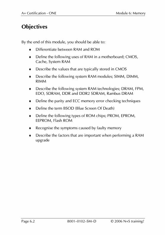
Objectives
By the end of this module, you should be able to:
♦ Differentiate between RAM and ROM
♦ Define the following uses of RAM in a motherboard; CMOS, Cache, System RAM
♦ Describe the values that are typically stored in CMOS
♦ Describe the following system RAM modules; SIMM, DIMM, RIMM
♦ Describe the following system RAM technologies; DRAM, FPM, EDO, SDRAM, DDR and DDR2 SDRAM, Rambus DRAM
♦ Define the parity and ECC memory error checking techniques
♦ Define the term BSOD (Blue Screen Of Death)
♦ Define the following types of ROM chips; PROM, EPROM, EEPROM, Flash ROM
♦ Recognise the symptoms caused by faulty memory
♦ Describe the factors that are important when performing a RAM upgrade

A+ Certification - ONE Module 6: Memory
© 2006 N+S training! 8001–0102–SM–D Page 6.3
Introduction to Memory When we refer to memory in a computer, we usually mean the electronic chips which are used to store programs and data, ready for use by the CPU. It can be attached to the system board via special interfaces (or slots). It can be built into the motherboard or the processor card, as cache memory. Small amounts of very fast memory, called registers, are also part of each CPU.
However, this on-board memory is only part of the data storage requirements of a PC. Data can also be stored on disk or tape. We will look at disk and tape storage in a later module.
We shall begin by looking at why there is a range of different data storage technologies. Then we shall spend the rest of this module looking at solid state memory.
Data Storage and Memory A computer needs to process data according to program instructions. Both instructions and data must be read into the CPU, which actually carries out the processing. There is little space on the CPU to hold information, so the instructions and data need to be read in small chunks, often just a few bytes at a time, and the results stored elsewhere, while the next set of instructions and data are read in and processed. The temporary storage areas in the CPU itself are called registers, there are generally only a few – a dozen or so, depending on the model of CPU. They are usually no larger than the data bus or some small multiple of it. Typical data bus widths are now 64 bits.
The data and programs used by the CPU are usually stored permanently on the hard disk, and so are any permanent results of data processing. However, disk access is very slow in comparison to the speed with which data can be moved around purely electronic circuits. So, even the earliest PCs used electronic memory to hold some of the data temporarily, where the CPU could access it much faster (by a factor of a thousand or more). This memory is referred to as the main memory or system RAM (Random Access Memory).
The trick is to read into the memory, from disk, the instructions and data that are likely to be required by the CPU. Then the CPU can access the information it needs from memory very quickly. This process is known

A+ Certification - ONE Module 6: Memory
Page 6.4 8001–0102–SM–D © 2006 N+S training!
as caching. The amount of memory is usually less than the amount of disk storage, because memory is more expensive than disk storage. Sometimes, the information needed will not be in memory and new information must be read from disk into memory, in the process overwriting information that is no longer required.
Faster
More Expensive
Less Data
Slower
Cheaper
More Data
RAMCPU DISK
Faster
More Expensive
Less Data
Slower
Cheaper
More Data
RAMCPU DISK
Figure 6.1 – The memory compromise
This approach provides a compromise between speed and cost, as shown here.
Although disks are used to store programs and data permanently, they can also be used as temporary storage which cannot be held in main memory, because it is full. This process is known as paging or swapping, and is covered in more detail in A+ TWO course.
All of the storage methods just described are examples of online storage – directly accessible by the PC as soon as it is powered on. To complete the picture, we should also mention offline storage, such as tapes; used for backing up and archiving data, which can then be stored at another location.
RAMCPU DISK
Faster
More Expensive
Less Data
Slower
Cheaper
More Data
TAPECACHE
Online Storage Offline Storage
Figure 6.2 - Online and Offline Storage

A+ Certification - ONE Module 6: Memory
© 2006 N+S training! 8001–0102–SM–D Page 6.5
Optical, Magnetic and Solid State Memory CDs and DVDs use optical methods for storing and retrieving data; 1s and 0s are stored in a form which can be read using light (typically lasers) and optical sensors. Hard disk drives, floppy disks and tapes use magnetic methods for storing and retrieving data; 1s and 0s are stored in a form which can be detected as magnetic fields of varying polarity.
Solid state memory uses circuits to store and retrieve data; 1s and 0s are stored as small electrical charges of varying voltages held in circuits. There are no moving parts required to read or write solid state memory.
Solid state memory can be categorised as volatile (RAM) or non-volatile (ROM). Optical and magnetic storage are described in later modules of this course, in this module we will describe RAM and ROM solid state memory.
RAM The contents of RAM memory are lost whenever the power is turned off, or when the operating system is rebooted – it is volatile.
RAM’s functions in a PC are to store BIOS configuration information (CMOS RAM), to provide primary storage for programmes that are running and files that are open (system RAM), and to provide a high-speed buffer for the most frequently used data and programme instructions (cache RAM).
Cache RAM is built using SRAM (Static RAM) chips.
System RAM is built using DRAM (Dynamic RAM) chips.
ROM The contents of ROM memory are not lost when the power is turned off or the PC rebooted – it is non-volatile.
When the PC boots up, some programs need to be made available to the CPU even before the operating system is loaded from the hard disk drive. An obvious example of this is the program that actually loads the operating system from disk to RAM. These programs, often referred to as the BIOS (Basic Input/Output System), are contained in a ROM chip.

A+ Certification - ONE Module 6: Memory
Page 6.6 8001–0102–SM–D © 2006 N+S training!
ROM memory can be permanent or re-programmable. Early versions of ROM chips were permanent – the information on them could not be modified. The contents of most modern ROM chips can be re-programmed by software; a process called flashing, hence the term flash BIOS.
Summary
There are two types of solid state memory; RAM and ROM.
RAM is volatile; it must have power supplied to it constantly or the data held in it is lost. System RAM is used to store programs that are running and files that are open. These programs and files are loaded (copied) from optical or magnetic storage into RAM as and when required.
Types of RAM chip include SRAM (used for cache memory) and DRAM (used for system memory).
ROM is non-volatile; it retains data even if there is no power present. ROM is used to store essential system programs, such as the motherboard’s BIOS.
Knowledge Check 6.1
Which type of memory does not require any power to hold its contents?
ROM

A+ Certification - ONE Module 6: Memory
© 2006 N+S training! 8001–0102–SM–D Page 6.7
RAM Now we will examine some of the uses of solid state memory in a PC, starting with RAM. The figure below shows some of the functions of RAM in a typical PC; cache RAM, system RAM and CMOS RAM.
CPU
System RA
M
-D
RAM
NorthbridgeChipset
L2 cacheSRA
M
BIOS - ROMBIOS - ROM
SouthbridgeChipset
CMOS - RAMCMOS - RAM
CPU
System RA
M
-D
RAM
NorthbridgeChipset
L2 cacheSRA
M
BIOS - ROMBIOS - ROM
SouthbridgeChipset
CMOS - RAMCMOS - RAM
L1 cache
Figure 6.3 – RAM functions
CMOS RAM The basic concept of CMOS RAM has already been discussed in Module 3 – Motherboards, so a brief recap is provided here. CMOS is the storage area for the PC’s configuration data. Like most forms of RAM, CMOS is volatile so to retain information while the PC is switched off or rebooted it requires a battery on the motherboard.
In this section we will focus more on the values that are held in the CMOS RAM and their purpose.

A+ Certification - ONE Module 6: Memory
Page 6.8 8001–0102–SM–D © 2006 N+S training!
Values held in the CMOS RAM include:
Value Purpose
Date and time The ‘real’ date and time is maintained in CMOS. This value can be changed using the BIOS setup program, but it can also be altered from within the operating system (ie Windows or Linux).
Boot sequence When a PC is booted, an operating system will be loaded into system RAM. Operating systems can be loaded from a variety of locations, including floppy, hard drive, CD or DVD or from another computer via a network card. CMOS stores the sequence in which these devices are scanned for an operating system.
Hard drives In order to communicate properly with a hard drive, the PC must know what type of hard drive is installed. The information stored in CMOS will be the hard drive’s geometry. This includes number of read/write heads, number of sectors per track, and the access method such as PIO and DMA modes (these settings are discussed in more depth in Module 7 – Data Storage Devices). Unless you have a very old hard disk drive these values will be set automatically, as modern hard disk drives are able to communicate this information to the BIOS.
Floppy drives As with hard disk drives, the PC must know what type of floppy drive is installed to communicate successfully with it. CMOS will store the floppy drive type eg 3.5” 1.44 MB

A+ Certification - ONE Module 6: Memory
© 2006 N+S training! 8001–0102–SM–D Page 6.9
Value Purpose
Power management Most BIOSs have a feature built into them called APM (Advanced Power Management). This allows the BIOS to put devices such as hard disk drives and monitors into a low-power consumption (standby) mode. CMOS can reflect whether the APM feature is enabled or disabled, and the length of inactive time before a device is put into standby.
Just like the date and time, modern operating systems can also control APM settings using programs collectively called ACPI (Advanced Configuration and Power Interface). CMOS can reflect whether this option is enabled or disabled.
CPU clock speeds You may remember that the CPU speed is dictated by a system clock. The system clock speed and the multiplication factor for determining the CPU speed may be stored in CMOS. Some motherboards may use jumpers rather than CMOS settings for these values.
Some CPUs, in order to protect themselves from overheating, may ignore any CMOS settings that would cause them to run faster than their correct speed (ie they prevent overclocking).

A+ Certification - ONE Module 6: Memory
Page 6.10 8001–0102–SM–D © 2006 N+S training!
Value Purpose
Passwords Some BIOS setup programs provide password protection to prevent unauthorised alteration of CMOS settings. Any such passwords are stored in CMOS.
If the password is forgotten it may be cleared by altering a jumper setting on the motherboard. If this option is not available, removing the CMOS battery from the motherboard for a few minutes will have the same effect, although this technique will also clear all other settings.
CMOS does not store your Windows passwords.
Enabled/Disabled devices
Many motherboards have built-in devices such as video cards. However, the on-board video card may become faulty, or the user may simply wish to use a different video card. In either case, the built-in video card will have to be disabled. CMOS can be configured to say which motherboard devices are enabled or disabled.
In addition to video cards, other devices that can be disabled include serial ports, parallel ports and IrDA (infra red) ports.
Plug and Play This is a simple enable/disable option that indicates whether BIOS is going to be working with a Plug and Play capable operating system such as Windows XP.

A+ Certification - ONE Module 6: Memory
© 2006 N+S training! 8001–0102–SM–D Page 6.11
Value Purpose
Virus protection Some BIOSs provide a very simple virus protection feature to protect the hard disk drives boot sector. CMOS is configured to indicate whether this option is enabled or disabled. This feature is not suitable for general virus protection of your data; you should install software such as Norton or McAfee for this.
Should any problems be encountered, most BIOS setup programs provide an option to reset all CMOS values to default settings.
Some PCs may not provide all of these options.
Cache RAM Earlier in this module we introduced the concept of using system RAM to cache information from the hard disk drive. Modern PCs carry this process further by having extra levels of specialised cache memory between the system RAM and the CPU. Some of the cache memory may be on the module holding the CPU itself, while some may be on the system board. Cache memory built directly into the CPU is known as Level 1 (or L1) cache. Level 2 (or L2) cache memory is separate from the CPU and is either mounted on the motherboard, or in the case of SEC packaged chips, it is mounted next to the CPU on the SEC card. Some PCs have three levels of cache memory.
Cache memory is constructed from SRAM (Static RAM) chips. The first thing to clarify is that SRAM is still volatile; it needs a constant power source to retain the 1s and 0s held in it. It is not the same as Flash RAM which does not need a power source.
As you will learn, DRAM requires refreshes to maintain the voltages representing the 1s and 0s in the memory circuits. SRAM does not require refreshes. This means that SRAM is faster to access than DRAM, as there are no ‘wait states’ encountered while memory refreshes occur.
However, the physical composition of SRAM is more expensive to produce than DRAM, so SRAM is used where speed is critical and cost is not. The PC’s caches are typically constructed from SRAM.

A+ Certification - ONE Module 6: Memory
Page 6.12 8001–0102–SM–D © 2006 N+S training!
The amount of cache memory that can be installed in any particular system is defined by the model of chipset that the motherboard uses.
System RAM Whenever a program is started, or a file opened, it is read from secondary storage such as a hard disk or CD-ROM into system RAM.
System RAM forms the largest block of memory in the PC; typically between 512 MB and 1 GB.
System RAM is found attached to the motherboard in the form of DRAM chips mounted on a small circuit board known as a memory module. There are a variety of DRAM types, including FPM, EDO, SDRAM, DDR SDRAM and RDRAM.
DRAM chips are mounted on small circuit boards called SIMM, DIMM and RIMM memory modules.
System RAM upgrades are quite possibly one of the most frequently performed tasks, as adding more system RAM to a PC can make a dramatic improvement in performance.
In order to upgrade a PC’s system RAM, you should understand the various memory modules, and the memory types that they provide.
Summary
CMOS RAM stores the PC’s hardware configuration data.
Cache RAM is a high-speed buffer used by the CPU. Cache RAM is built from SRAM chips.
System RAM holds all currently active program instructions and data. System RAM is built from DRAM chips.
There are a variety of DRAM types including FPM, EDO, SDRAM, DDR SDRAM and RDRAM.
DRAM chips are mounted on memory modules called SIMM, DIMM and RIMM.

A+ Certification - ONE Module 6: Memory
© 2006 N+S training! 8001–0102–SM–D Page 6.13
Knowledge Check 6.2
Name three uses for RAM in a PC.
CMOS, Cache, System RAM. What type of RAM is cache made of?
SRAM. What type of RAM is System RAM made of?
DRAM. Name three types of DRAM
Choose any three from FPM, EDO, SDRAM, DDR SDRAM and RDRAM

A+ Certification - ONE Module 6: Memory
Page 6.14 8001–0102–SM–D © 2006 N+S training!
System RAM Memory Modules Early PC’s system RAM was provided in the form of DIP (Dual Inline Package) chips. DIP chips are rectangular and have a row of pins along each of their long sides.
These were inserted in banks of eight chips (nine if the system used memory parity checking – see later) in sockets on the motherboard.
Figure 6.4 – DIP
When installing DIP chips it was very easy to misalign the pins in their sockets, causing the pins to bend. The chip would then have to be removed, the pins straightened, and the chip re-seated in its socket. Because the pins were quite delicate, it was common for the pins to break off, rendering the chip unusable.
To counteract this problem, memory manufacturers devised the concept of memory modules. The required eight or nine chips were pre-mounted on a small circuit board which could be attached to the motherboard using an edge connector rather than pins.
The first memory modules were called SIMMs (Single Inline Memory Modules).
The legs either side of the chips mounted on a memory module such as a DIMM do not have to penetrate the circuit board; they are surface-mounted. Therefore the pins protrude less from the chip than they do on a DIP, which has to ‘poke’ into a socket. Because of this difference, the chips mounted on a memory module are called TSOPs (Thin Small Outline Packages).
Figure 6.5 - TSOP
SIMM SIMMs (Single In-Line Memory Modules) are miniature circuit boards with edge connectors, to which RAM chips are fixed. The SIMM is then inserted into a slot on the motherboard. The connectors of the SIMM

A+ Certification - ONE Module 6: Memory
© 2006 N+S training! 8001–0102–SM–D Page 6.15
and the SIMM slot on the motherboard are either gold or tin and should not be mixed together, ie a SIMM with gold contacts should not be placed in a SIMM socket with tin contacts. SIMMs are available in two sizes: 30- and 72-pin.
30-Pin SIMMs – these have an address width of 8 bits – meaning they can transfer 8 bits of data at a time across the memory bus. Some 30-pin SIMMs also include a parity bit for error detection (so these are 9 bits wide). A 30-pin SIMM typically contains 1 MB or 4 MB of RAM. They have a single notch on the bottom left to ensure that they are installed correctly.
Figure 6.6 - 30-pin SIMM
72-Pin SIMMs – these have an address width of 32 bits, or 36 bits if they include parity bits (a parity bit is included for each byte of data; as 32 bits equals 4 bytes there are 4 parity bits included in addition to the data bits). A 72-pin SIMM typically contains 4, 8, 16, 32 or 64 MB of RAM. They have one notch at the side and one notch in the centre of the module.
Figure 6.7 - 72-pin SIMM
Because Pentium systems access 64 bits of data at a time from memory, older Pentium motherboards that implemented 72-pin SIMM memory slots required two 72-pin SIMM cards to be installed at a time. In other words, the two 32-bit, 72-pin cards were electronically combined together to form a 64-bit bank of memory.
DIMM A SIMM has metal connectors along each side of its bottom edges that provide contact with the motherboard SIMM socket. However, these

A+ Certification - ONE Module 6: Memory
Page 6.16 8001–0102–SM–D © 2006 N+S training!
connectors effectively run straight through the card and are therefore really just one set of connectors. A DIMM has similar metal connectors, but each side is independent of the other – hence Dual Inline Memory Module. Modern motherboards use 168-, 184-or 240-pin DIMMs.
168-pin DIMMs have two small notches within the row of pins along the bottom of the module. 184- and 240-pin DIMMs only have one notch within the row of pins, but positioned differently to prevent the wrong type of DIMM being placed in the wrong type of socket. You will see these notches if you look carefully at the bottom edge of the cards in the figures below.
Table 6.1 - DIMMs
Figure 6.8 - 168-pin
Figure 6.9 - 184-pin
Figure 6.10 - 240-pin
DIMMs require 3.3 Volts or less, consuming less power than SIMMs, which require 5 Volts. Typical DIMM card capacities are 32 MB to 1 GB.
Some early motherboard designs provide sockets for banks of both SIMMs and DIMMs. Care must be taken when populating these with both SIMMs and DIMMs, as not all combinations of SIMMs and DIMMs may be supported. Check the motherboard manual or manufacturer’s web site to ensure that you install a valid combination.
RIMM RIMM is the name for a Rambus memory module (see later in this module for a description of Rambus). RIMMs are similar in appearance to DIMMs. The faster access times and transfer speeds lead to the generation of more heat than with other memory technologies. Because of this, an aluminium sheath called a heat spreader is used to cover the module in order to protect the chips from overheating. RIMMs have

A+ Certification - ONE Module 6: Memory
© 2006 N+S training! 8001–0102–SM–D Page 6.17
184 pins, but to prevent their accidental insertion into a 184-pin DIMM socket the notches along the bottom edge are placed in different positions (compare the figure below to Figure 6.9)
Figure 6.11 – RIMM
Unlike DIMM memory slots, RIMM memory slots should not be left empty. Special C-RIMM (Continuity RIMM) cards should be inserted into empty slots to provide a continuous pathway for signals. C-RIMM cards do not have any memory chips on them, so they are relatively very cheap.
Figure 6.12 - RIMM and C-RIMMs
RamBus technology is considered redundant; Intel for example essentially dropped the use of Rambus memory from all of its products since 2004. This may be due to the fact that Rambus Inc. – the inventors of Rambus memory – filed several aggressive lawsuits against other memory manufacturers, claiming that they had stolen their technology. This undoubtedly would have cast RamBus Inc. in an unfavourable light.

A+ Certification - ONE Module 6: Memory
Page 6.18 8001–0102–SM–D © 2006 N+S training!
Summary
Very old PCs such as those based on a 486 CPU use 30-pin SIMMs.
Slightly later PCs such as those based on an early Pentium CPU use 72-pin SIMMs. Remember that Pentium systems using 72-pin memory cards must have pairs of these SIMMs installed.
Most modern Pentium PCs will use 168-, 184-, or 240-pin DIMMs.
Some PCs may use RIMMs.
Knowledge Check 6.3
Name the three main types of memory module used in a PC’s motherboard.
SIMM, DIMM, RIMM. How many pins might a DIMM have?
168, 184, or 240.

A+ Certification - ONE Module 6: Memory
© 2006 N+S training! 8001–0102–SM–D Page 6.19
System RAM Technologies You have just learnt about various types of memory module (SIMM, DIMM, and RIMM). Each SIMM, DIMM or RIMM has a number of chips soldered onto it. Next you will learn more about the types of memory chip that you will find on a SIMM, DIMM or RIMM.
DRAM The first PCs used ‘ordinary’ DRAM (Dynamic RAM) chips. DRAM memory chips are provided on 30-pin SIMM modules used in 80286 and 80386-based PCs.
DRAM memory employs a semi-conductor that stores discrete ‘ones’ or ‘zeros’ using a miniature capacitor and transistor. The electrical charge held within the semi-conductor gradually weakens through leakage. To prevent data loss, the charge must be periodically refreshed. While the charge is being refreshed, the data cannot be read or modified, so the CPU may have to enter what is called a ‘wait-state’ while the charge is refreshed. This slows the operation of DRAM.
Many variations of DRAM exists, each with its own features for improving performance, these are now described.
FPM FPM (Fast Page Mode) DRAM memory chips are provided on 72-pin SIMM modules and, very rarely, on 168-pin DIMM modules. These would be found on original Pentium and even 80486 based PCs.
Prior to 1995, Fast Page Mode was the most common form of memory found in PCs. It was often referred to simply as DRAM. FPM had an advantage over earlier memory types, as it enabled faster access to data located within the same memory row as the initial access (you can think of memory as like a spreadsheet, where information is organized in rows and columns).
EDO EDO (Extended Data Out) memory chips are provided on 72-pin SIMM modules and, very rarely, on 168-pin DIMM modules. These would be found on more mature Pentium-based PCs such as the original Pentium, Celeron Pentium II and Xeon Pentium III.

A+ Certification - ONE Module 6: Memory
Page 6.20 8001–0102–SM–D © 2006 N+S training!
The next major innovation in memory technology came in 1995, with the introduction of EDO. Consecutive memory accesses could be handled much faster. The extra speed led to the memory controller reducing the number of steps required in the addressing process. EDO enabled the CPU to access memory approximately 10 to 15% faster than with FPM.
SDRAM SDRAM memory chips are provided on 168-pin DIMM modules. SDRAM is commonly found in Pentium II and Pentium III based PCs.
In 1996, Synchronous DRAM became common in PCs. SDRAM synchronises with the timing of the CPU, enabling the memory controller to ‘know’ the exact clock cycle when the requested data becomes available. The CPU no longer has to enter a wait-state between memory accesses. SDRAM memory can also use interleaving and burst mode functions, which leads to even faster data retrieval. SDRAM chips are available in several different speeds, so that they can be synchronised to the clock speeds of the PCs in which they will be installed. For example, PC133 SDRAM runs at 133 MHz. Faster SDRAM speeds such as 200 MHz and 266 MHz are available.
Table 6.2 - SDRAM Modules
Module name Chip technology Speed (MHz) Form factor
PC100 SDRAM 100 168-pin
PC133 SDRAM 133 168-pin
DDR and DDR2 SDRAM DDR SDRAM (Double Data Rate SDRAM) memory chips are provided on 184-pin DIMM memory modules. DDR2 SDRAM memory chips are provided on 240-pin DIMM modules. DDR and DDR2 SDRAM is commonly used by Pentium 4 based PCs.

A+ Certification - ONE Module 6: Memory
© 2006 N+S training! 8001–0102–SM–D Page 6.21
DDR2, as its name suggests, is simply an enhancement of DDR memory that provides faster speeds, higher data bandwidths, lower power consumption, and enhanced thermal performance over DDR.
Figure 6.13 - DDR2 logo
The following information therefore applies to both DDR and DDR2 memory. DDR SDRAM is an extremely fast SDRAM technology. Ordinary SDRAM memory works from a clock signal. The clock signal is constantly changing from a low to a high, then back to a low voltage. SDRAM only acts when the clock voltage changes from low to high. DDR SDRAM memory chips can act when the clock changes from low to high, and high to low, effectively doubling the data transfer rate. For example, with DDR SDRAM, a 133 MHz memory bus clock speed leads to an effective data rate of 266 MHz.
Table 6.3 - DDR SDRAM Modules
Module name Chip technology Speed (MHz) Form factor
PC1600 DDR SDRAM 200 184-pin
PC2100 DDR SDRAM 266 184-pin
PC2700 DDR SDRAM 333 184-pin
PC3200 DDR SDRAM 400 184-pin
PC4000 DDR SDRAM 500 184-pin
PC2-3200 DDR2 SDRAM 400 240-pin
PC2-4200 DDR2 SDRAM 533 240-pin
PC2-5300 DDR2 SDRAM 667 240-pin
PC2-6400 DDR2 SDRAM 800 240-pin
Rambus DRAM As its name clearly suggests, Rambus DRAM (sometimes called RDRAM) is another type of DRAM. Rambus DRAM was invented by a company called Rambus Inc. who licence their technology to other manufacturers who produce this type of memory.

A+ Certification - ONE Module 6: Memory
Page 6.22 8001–0102–SM–D © 2006 N+S training!
Rambus DRAM is more commonly found in gaming computers such as the Nintendo 64 and Sony Playstation 2, although some PCs do use it, eg the Dell Precision Workstation 420 and Compaq Deskpro AP240.
Rambus DRAM memory chips are mounted on a special memory module called a RIMM, which has been described earlier in this module.
Summary
There is a variety of DRAM types used in PCs.
DRAM – found on 30-pin SIMM modules.
FPM – usually found on 72-pin SIMM modules
EDO – usually found on 72-pin SIMM modules
SDRAM – found on 168-pin DIMM modules
DDR-SDRAM – found on 184-pin DIMM modules
DDR2-SDRAM – found on 240-pin DIMM modules
Rambus DRAM – found on RIMM modules
A+ Certification - ONE Module 6: Memory
© 2006 N+S training! 8001–0102–SM–D Page 6.23
Memory Module Characteristics You have just learnt that each memory module has a number of RAM chips soldered onto it. The most commonly used type of memory module is a DIMM, the most commonly used types of RAM chips are SDRAM, DDR SDRAM or DDR2 SDRAM.
Memory modules, such as DIMMs, also differ from each other in other respects, such as the number of chips mounted on them, the amount of memory they contain, the way they cope with errors and so on. We will discuss these characteristics now.
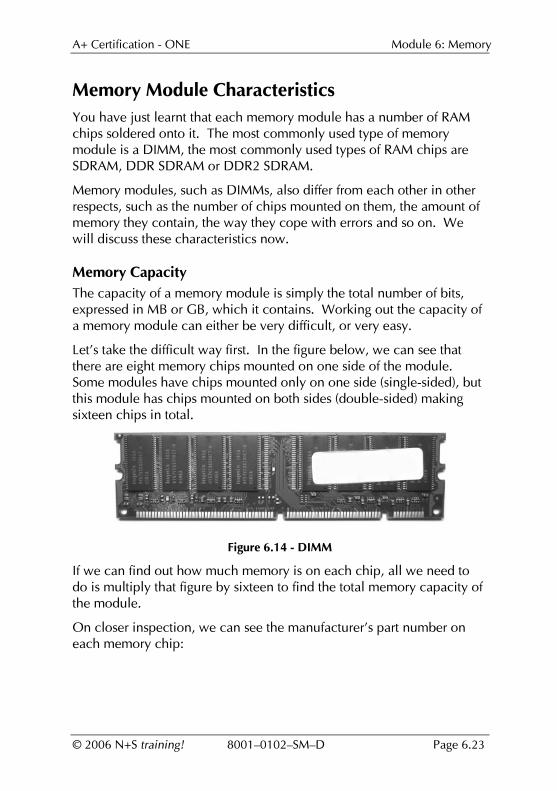
Memory Capacity The capacity of a memory module is simply the total number of bits, expressed in MB or GB, which it contains. Working out the capacity of a memory module can either be very difficult, or very easy.
Let’s take the difficult way first. In the figure below, we can see that there are eight memory chips mounted on one side of the module. Some modules have chips mounted only on one side (single-sided), but this module has chips mounted on both sides (double-sided) making sixteen chips in total.
Figure 6.14 - DIMM
If we can find out how much memory is on each chip, all we need to do is multiply that figure by sixteen to find the total memory capacity of the module.
On closer inspection, we can see the manufacturer’s part number on each memory chip:

A+ Certification - ONE Module 6: Memory
Page 6.24 8001–0102–SM–D © 2006 N+S training!
Figure 6.15 – Chip model
Luckily, a search of the manufacturer’s (Hynix) website reveals the information we need about his chip:
Part No. Organization
HY57V28820HC(L)T-H(I) 4 banks of 4Mx8
Memory capacity of chips and modules is often shown in expressions like these; 4Mx8, 8Mx16, or 16Mx64. Think of these expressions like spreadsheets, where for example, a 4Mx8 chip has 4 million (4M) rows of memory 8 columns (x8) wide. Each cell of this spreadsheet is one bit of memory. So, a 4Mx8 chip has 32 million bits of memory (4 million times 8 = 32 million). To express this in bytes we simply divide the total by 8, giving us 4 MB. The chip shown above has 4 banks of 4 MB within it; therefore the chip contains 16 MB of RAM. As there are 16 of these chips on our example DIMM, this means the DIMM contains 256 MB (16 MB x 16 = 256 MB).
For our example DIMM, there is a much easier way of determining its capacity. On one side of the chip is a label:
Figure 6.16 - DIMM Label

A+ Certification - ONE Module 6: Memory
© 2006 N+S training! 8001–0102–SM–D Page 6.25
As you can clearly see in the highlighted area, this is a 256 MB DIMM. Notice how we are also shown the memory organization of the whole module to the right of its capacity (32Mx64). So, the memory on this module is presented to the system as 32 million rows that are 64 bits wide.
32 million x 64 = 2048 megabits
2048 megabits / 8 = 265 MB
Summary
The capacity of a module is usually shown on a label stuck to it.
If a label is not present, then the capacity of the module can be determined by finding out the capacity of the chips on the module, and then multiplying that value by the number of chips.
For example, a module with sixteen 64 megabit chips has a capacity of 128 MB calculated as follows:
16 x 64 megabit = 1024 megabits
1024 megabit / 8 = 128 megabytes
Error Detection Bits can be changed from 1 to 0 or vice versa by an unexpected alteration of the voltage levels in a memory cell. This change of voltage is most likely caused by cosmic rays – yes, really. Because this change is non-permanent it is known as a soft error. If the affected bit is not used by your system, you may never know there was a soft error. If the bit does get used then the result may be that your system or application hangs or crashes. Soft errors are simply corrected by rebooting the PC.
For critical systems, such as servers, it would be better if there were some method of detecting if a value in RAM has been altered inadvertently, and if possible, correcting that alteration.
There are two methods of memory error detection; parity checking and ECC.

A+ Certification - ONE Module 6: Memory
Page 6.26 8001–0102–SM–D © 2006 N+S training!
Parity checking techniques are used to ensure the reliability of data. This requires an additional parity bit for each byte (so a parity-checked byte will consist of 9 rather than 8 bits), causing parity-checking memory too be more expensive than non-parity memory.
Parity checking uses a very simple algorithm for detecting single-bit errors. The bits set to 1 (ON) in a byte are totalled, and then the parity bit is set to either 1 (ON) or 0 (OFF) to make the total an odd or an even number (depending on whether the system is designed to perform odd or even parity checking).
Byte Parity bit Number of ON bits Parity
00101000 0 Two Even
11111000 1 Six Even
The table above shows a system that performs even parity checking.
In the first row of the table the byte in the first column (00101000) contains two ON bits. As two is an even number, the parity bit will be set to 0 to make the total number of ON bits remain at two – an even number.
In the second row of the table the byte in the first column (11111000) contains five ON bits. As five is an odd number, the parity bit will be set to 1 to make the total number of ON bits six – again, an even number.
If any byte of memory, plus its parity bit, is read that contains an odd number of bits, then the memory checking circuitry signals an error to the CPU using a special interrupt called the Non-Maskable Interrupt. The CPU cannot ignore this interrupt and must service it immediately.
Upon encountering a parity error, most systems will give a BSOD (Blue Screen Of Death). That is, the screen will turn completely blue, with a basic error message in white text at the top of the screen indicating a parity error. This is a situation that can only be resolved by completely rebooting the system.
PC specifications should indicate whether parity checking memory is required or not. The two types of memory cannot be used together in the same computer. Some BIOS programmes allow parity memory to be turned on or off.

A+ Certification - ONE Module 6: Memory
© 2006 N+S training! 8001–0102–SM–D Page 6.27
A more advanced error checking technique is Error Correcting Code (ECC). ECC uses more sophisticated mathematical algorithms to detect memory errors than parity checking does. Unlike parity checking, ECC does not work on individual bytes, but on blocks of either 4 or 8 bytes, requiring 7 or 8 bits respectively for the required error correcting information. Within these blocks of memory, ECC can both detect and fix single-bit errors and detect (but not fix) two-bit errors.
As with parity checking, the motherboard’s BIOS and chipset must be capable of supporting ECC, and the BIOS may allow ECC to be turned on or off.
Error correction with ECC is transparent to the user – ie the error is fixed without any error message being displayed on the screen. Two-bit errors however, which are detected but not fixed, will likely cause a BSOD.
Memory errors are relatively rare, rare enough in fact that for standard uses (such as a desktop PC) non-parity or non-ECC is usually used. You can see from the label on our example DIMM that it does not use ECC (nonECC).
Figure 6.17 - nonECC DIMM
Parity or ECC memory is more often found in servers, where all efforts must be made to create a stable system.

A+ Certification - ONE Module 6: Memory
Page 6.28 8001–0102–SM–D © 2006 N+S training!
Summary
Errors in memory can have serious impact on data or the operation of the machine. Therefore it is vital that in critical systems, memory errors are at least detected, if not fixed.
Parity checking can detect only single-bit errors, but not fix them.
ECC can detect and fix single-bit errors, and detect but not fix errors of more than one bit.
Uncorrected errors typically cause a BSOD (Blue Screen Of Death).
Registered Modules Registered memory modules have extra circuitry on them that ensures the signals sent through the memory chips remain strong, clear and constant. Not only does this reduce the number of errors that might occur when reading or writing memory, it also allows a module to be built using more chips and therefore a higher capacity.
Like ECC, registered modules are typically only found in servers; most desktop PCs will use non-registered memory.
Older memory modules used a similar feature called buffering; you might therefore see modules referred to as buffered or unbuffered as in the example below.
Figure 6.18 - Unbuffered DIMM

A+ Certification - ONE Module 6: Memory
© 2006 N+S training! 8001–0102–SM–D Page 6.29
Troubleshooting RAM Faulty RAM can cause a PC to behave erratically; it can reboot randomly, it can give errors during the POST, or might occasionally lock up or crash with a Blue Screen of Death. There are many things that can cause these symptoms, including an overheating or faulty CPU, a faulty motherboard component, but it could equally be faulty memory.
To try to determine if memory is causing these problems there are a variety of tools and methods available to the PC support technician.
Using POST A system RAM test is usually performed every time the PC is turned on. This test is performed by the POST (Power On Self Test) routine in the motherboard’s BIOS chip.
POST memory tests will usually display a rapidly advancing number on the screen indicating the amount of memory that has been tested. This number should match the amount that has been installed. So if you have 512 MB of system RAM installed you should see something similar to the figure below.
Figure 6.19 - POST RAM Test
If this number is not what you expected, it could be that an incorrectly configured bank of memory modules is being ignored by the POST. This is a fundamental but important step in determining memory errors.

A+ Certification - ONE Module 6: Memory
Page 6.30 8001–0102–SM–D © 2006 N+S training!
It is possible that these details will be hidden from the display when a PC boots up. This is usually an option that can be altered from the BIOS Setup program, which in the example above, would be executed by pressing DEL at this point.
Although the POST memory test will not perform an exhaustive test of your system RAM, it should at least indicate the following errors:
♦ No memory recognised
♦ Faulty memory module
♦ Incorrectly configured memory module
These errors would be accompanied by a beep code from the POST programme that indicates the exact nature of the problem, and if possible, an error message on the screen. Sometimes, especially in the case of there being no available memory, it would not be possible to display an error code on the screen, so just a beep code would be issued.
A description of beep codes is provided in the Motherboard module in this manual.
So, if we reboot our faulty PC and the POST does not indicate any errors, we can assume that the system RAM recognised and configured correctly. However, the POST will only perform a very basic check of the integrity of each memory cell in our RAM chips. To test these more thoroughly we need another programme.
Using Third-Party Tools A more exhaustive test of system RAM can be accomplished using third-party utilities. In the example shown below, a free utility called Memtest-86 has been downloaded from the Internet. This utility creates a floppy disk which the computer is then booted from. The Memtest-86 program then starts a test which writes random bit patterns to every piece of system RAM and then reads them back in again. Should there be any differences between the bits written and the bits read an error is indicated.

A+ Certification - ONE Module 6: Memory
© 2006 N+S training! 8001–0102–SM–D Page 6.31
Figure 6.20 – Memtest-86
This test should be left running for several hours, or even days in the case of critical systems such as servers, to ensure that a very thorough test is performed.
If errors are indicated by this programme, we have located the fault in our PC. If no errors are indicated, we have at least done all that we can to eliminate our system RAM as the cause of the erratic behaviour.
Summary
RAM errors can cause problems booting the PC. These types of errors should be indicated by beeps during boot up. When a PC boots, listen carefully for any beep codes and take the appropriate action – usually this means replacing a memory card.
RAM errors can also cause erratic behaviour – the PC may hang, reboot or crash with a Blue Screen of Death. If rebooting the PC does not solve this problem, you might want to consider running a third-party programme to thoroughly test your memory.

A+ Certification - ONE Module 6: Memory
Page 6.32 8001–0102–SM–D © 2006 N+S training!
Installing RAM Adding more system RAM is one of the most commonly performed PC upgrades. Adding more system RAM invariably improves system performance, especially where memory-hungry software - such as Windows - is being used.
If your system RAM is full, and you try to load up another programme or file, space in system RAM has to be created for it. Windows does this by logically dividing system RAM into 4kB sections called pages. A table is maintained that indicates how recently each page has been referenced. When more RAM is required, Windows locates the least recently referenced pages and copies them to a special area on the hard disk drive called the Swap or Paging file. When enough pages have been freed up in this way the new programme or file can be loaded.
This technique is called Virtual Memory, and has the benefit of allowing you to open up more programmes and files than you would otherwise have room for. There is of course a penalty to be paid; when information that has been written to the swap file is required, it has to be copied back into RAM, perhaps at the expense of other pages which have to be swapped back to the hard disk. This increased hard disk activity will have an adverse affect on performance.
Ideally we would keep everything in RAM. This isn’t always possible, but certainly, the more RAM that you have, the less likely it is that paging to and from the hard disk will occur.
You will learn more about Virtual Memory in the A+ TWO course.
Let’s say that a friend of ours bought their first PC six months ago to do a little web surfing and emailing. Initially they were perfectly happy with the performance of their machine. Recently though our friend started to use their PC for home publishing, and are using Microsoft Publisher, as well as Adobe PhotoShop, Illustrator and Acrobat to create sophisticated illustrated documents. They now notice, when all of these applications are opened, that their PC’s performance is severely degraded. The most likely cause of this is a shortage of system RAM while using these memory-hungry applications.

A+ Certification - ONE Module 6: Memory
© 2006 N+S training! 8001–0102–SM–D Page 6.33
So, let’s upgrade the system RAM. The first step is to determine the current memory configuration, and determine how much memory we can add.
Determining Currently Installed RAM Windows can show you how much physical RAM is installed. To do this, alternate-click on the My Computer icon and choose Properties, alternatively double-click the System icon in Control Panel.
The General tab in the resulting dialogue box will show you the amount of RAM that you have installed.
Figure 6.21 - Installed RAM using Windows
Alternatively, there are third-party programmes such as Lavalys’ Everest that can show you the same information.
Figure 6.22 - Installed RAM using Everest

A+ Certification - ONE Module 6: Memory
Page 6.34 8001–0102–SM–D © 2006 N+S training!
Determining Maximum RAM Next you will need to determine if the amount of RAM currently installed is the maximum supported by your motherboard or not.
Again, there is a variety of ways of doing this.
Using the PC Manual If your PC came with a manual, it may tell you the maximum amount of RAM supported.
Figure 6.23 - PC Manual
The figure above shows an extract from a Dell laptop owner’s manual.
If you don’t have the relevant documentation, you may find the equivalent information on the manufacturer’s website.
Looking up the Motherboard Specification If your PC does not have a manual, then your motherboard might (this is why, if you build your own PC, it is particularly important that you keep all the relevant documentation in a safe place). If you don’t have the documentation, but you know the manufacturer and model of your motherboard, then you may be able to find the relevant information on their website or using an Internet search engine.

A+ Certification - ONE Module 6: Memory
© 2006 N+S training! 8001–0102–SM–D Page 6.35
Figure 6.24 - Motherboard Specification
Once you have determined that you can add more memory to the current configuration, you should check that you have a spare memory slot on the motherboard. For example, your motherboard might support a maximum of 2 GB of RAM, and currently there is just 1 GB installed. However, the 1 GB of RAM might be configured as two 512 MB memory cards which are occupying the two available slots that your motherboard provides.
To check if you have spare slots, you can simply remove the lid of the system case and perform a visual check.
Determining Type of RAM So you have now determined, for example, that your computer supports 2 GB of RAM, you have only 1 GB installed, and you have a spare memory slot. You could now install another 1 GB of RAM in the unoccupied slot. Now you must determine what type of 1 GB memory card to buy. Again, the relevant documentation should help you to determine what you need.
There are also web-based memory suppliers that provide very useful tools to help you. If we wanted to buy 1 GB of RAM for a Dell Dimension 3000 PC. You could go to a memory provider such as Kingston Technology Company or Crucial Technology and use their search facilities:

A+ Certification - ONE Module 6: Memory
Page 6.36 8001–0102–SM–D © 2006 N+S training!
Figure 6.25 - Memory Search
The results of the search above tells us that each memory slot on our motherboard is compatible with memory cards containing 128, 256, 512 or 1024 MB of either DDR333 or DDR400 memory. If we refer back to our earlier Table 6.3 - DDR SDRAM Modules, we see the following information:
Mem
ory
Mod
ule
nam
e
Mem
ory
Tech
nolo
gy
Mem
ory
spee
d in
M
Hz
DIM
M F
orm
Fa
ctor
Vol
tage
PC2700 DDR 333 184-pin 2.5
PC3200 DDR 400 184-pin 2.8
So now we know what to order; a 184-pin DIMM with 1 GB of either PC2700 (DDR333) or PC3200 (DDR400) memory chips on it. It should now be an easy task to search any online supplier for this type of memory card to get the best price.

A+ Certification - ONE Module 6: Memory
© 2006 N+S training! 8001–0102–SM–D Page 6.37
Figure 6.26 – Buying Memory
Now all we have to do is place our order and wait for it to arrive.
Performing the Installation The difficult part is over; now that you have the memory you now just have to insert it into your motherboard.
Remember, memory chips are static-sensitive devices, so take all of the ESD precautions that you learnt about earlier.
First turn of your PC and remove all power cables.
Remove the lid from the system case.
Locate the empty DIMM memory slot; it will look something like this:
Figure 6.27 - DIMM Slot

A+ Certification - ONE Module 6: Memory
Page 6.38 8001–0102–SM–D © 2006 N+S training!
Make sure that the securing clips (the white levers at either end of the slot as shown in) are in their full open position by pushing them outwards as far as they will go, being careful, of course, not to break then off.
Figure 6.28 - Open securing clips
Line your new DIMM up with the slot so that it is at 90 degrees to the motherboard and the notch along the bottom edge of the card lines up with the small plastic bar in the DIMM slot.
Figure 6.29 - Insert DIMM
Push the DIMM card gently but firmly straight down into the slot. The securing clips should start to move inwards.
When you are sure that the DIMM card is as far down in the slot as it will go, push the securing clips inwards so that they are firmly securing the card.
Figure 6.30 - Secure DIMM
Replace the case lid, plug your PC back into the power and reboot.
If there are no POST errors, you should now be able to check that your new memory has been recognised by using the procedures described earlier under the heading Determining Currently Installed RAM on page 6.33.

A+ Certification - ONE Module 6: Memory
© 2006 N+S training! 8001–0102–SM–D Page 6.39
Summary
To add RAM to a PC you should:
Determine how much RAM is currently in the motherboard
Determine the maximum amount of RAM supported by your motherboard
If you can add more RAM, make sure that there is an available slot
Find out what type of memory your motherboard supports
Order it and install it!

A+ Certification - ONE Module 6: Memory
Page 6.40 8001–0102–SM–D © 2006 N+S training!
ROM ROM memory chips are typically used for storing system-level programmes, such as the motherboard’s BIOS. Adapter cards, such as network interface cards, may also provide their own on-board BIOS programmes.
The motherboard BIOS chip provides basic hardware functionality, as well as the POST (Power On Self Test) programme and a configuration programme. The configuration program can be launched by pressing a key when the PC is booted up. The key that needs to be pressed varies from PC to PC, but is typically a function key such as F1 or F2, the Del key, or the Esc key.
Network interface card BIOS programmes provide such features as the ability to connect to another computer, typically a server, and load the operating system from that computer into the PC’s RAM.

A+ Certification - ONE Module 6: Memory
© 2006 N+S training! 8001–0102–SM–D Page 6.41
ROM Technologies The different types of RAM (ie FPM, EDO, SDRAM, DDR SDRAM) are quite important, as you must buy the correct type of RAM for your motherboard when performing a RAM upgrade. There are also different types of ROM. However, the differences between them are less important to know, as you are unlikely to need to change any of the ROM chips on your motherboard or interface cards. But purely as a matter of interest, a description of different ROM technologies is provided below.
PROM A programmable read-only memory (PROM) is a form of ROM where the setting of each bit (0 or 1) is permanently set by a fuse or anti-fuse. The memory can be programmed just once after manufacturing by "blowing" the fuses (using a PROM blower), which is an irreversible process. Blowing a fuse opens a connection while blowing an anti-fuse closes a connection.
EPROM An EPROM cell acts like a permanently open or closed transistor. When the "floating gate" is charged, it holds the charge and impedes the flow of electrons from the control gate to the silicon. Charging is accomplished by applying 12v to the control gate, and erasure is accomplished under ultraviolet (UV) light.
A programmed EPROM retains its data for about ten to twenty years and can be read an unlimited number of times. The erasing window must be kept covered to prevent accidental erasure by sunlight. Old PC BIOS chips were often EPROMs, and the erasing window was often covered with a label containing the BIOS publisher's name, the BIOS revision, and a copyright notice.
Figure 6.31 – EPROM with label removed

A+ Certification - ONE Module 6: Memory
Page 6.42 8001–0102–SM–D © 2006 N+S training!
EEPROM EEPROMs have a lifespan of between 10K and 100K write cycles, which is considerably greater than the EPROMs that preceded them. Unlike EPROMs, which have to be placed under UV light for erasure, EEPROMs are erased while remaining resident on the motherboard. Like EPROMs, EEPROMS use a floating gate to hold a charge.
Figure 6.32 - EEPROM
Flash ROM Flash ROM is a development of the EEPROM chip, and its name was invented by Toshiba to express how much faster it could be rewritten ("in a flash").
Most modern motherboard BIOS chips are flash memory, making them easy to update. A description of how to update a motherboard flash BIOS chip is provided in the Motherboards module in this manual.
Flash ROM has uses apart from motherboard BIOS chips. Memory cards for cameras and USB pen drives also use flash ROM. These devices are discussed in depth in later modules.

A+ Certification - ONE Module 6: Memory
© 2006 N+S training! 8001–0102–SM–D Page 6.43
Review The two basic types of solid-state memory are RAM and ROM. RAM is volatile, ROM is non-volatile.
RAM is used most often used for CMOS, cache and system RAM.
Cache RAM is built using SRAM chips, system RAM is built using DRAM chips.
CMOS RAM is used to store system configuration information, such as date and time, boot sequence, hard and floppy drive types, clock speed settings, and which motherboard features are enabled or disabled.
Cache RAM is used as a buffer between the CPU and system RAM to improve performance.
System RAM is where running programmes and open files are located.
System RAM is provided in the form of a card called a memory module. Memory module types include SIMM, DIMM and RIMM.
SIMM modules usually have DRAM, FPM or EDO RAM chips on them.
DIMM modules usually have SDRAM, DDR-SDRAM or DDR2-SDRAM chips on them.
RIMM modules have RDRAM chips on them.
Some memory modules provide error checking capabilities such as parity checking or ECC.
Some memory modules provide performance-enhancing technologies such as buffering and registering.
When adding system RAM to a motherboard you must make sure that you buy the correct type of module, with the correct type of chips on them, and with compatible features such as ECC/non-ECC, registered/non-registered.
ROM is most often used for BIOS.

A+ Certification - ONE Module 6: Memory
Page 6.44 8001–0102–SM–D © 2006 N+S training!
Review Questions
1 You have configured a PC so that as soon as it is powered on, a password is required. Where would this password be stored?
CMOS RAM
2 Where in a PC is L1 cache?
Inside the CPU
3 What type of memory technology does L1 cache use?
SRAM
4 What type of RAM chips would you find on a PC3200 memory module?
DDR SDRAM
5 What type of computer is most likely to use ECC memory modules?
A server
6 If you have a defective memory module, what is most likely to report the error to you?
The POST
7 Your motherboard has two memory slots. Currently you have a 256 MB memory module in each of them giving you 512 MB of system RAM. How will you increase your system to 1024 MB of RAM?
You will need to buy a 1024 MB memory module, or two 512 MB memory modules. A single 512 MB module would not be enough because you will have to remove one of your 256 MB modules to free up a slot.
8 How to you fit a DIMM into a DIMM slot?
By moving the securing clips as far out as they will go, then pushing the DIMM straight down into the slot.