
Superconducting Optoelectronic Circuits for Neuromorphic ...
MODULE – 1
ANALOG ELECTRONIC CIRCUITS
OPTOELECTRONIC DEVICES
Optoelectronic Devices is the field that deals with study of devices that emit, detect and control light in the
wavelength spectrum ranging from ultraviolet to far infrared. They include electrical-to-optical (convert
electrical energy into light energy) and optical-to-electrical (convert light energy into electrical energy)
transducers. Optocouplers also come in this broad category.
PHOTODIODES:
Photodiode is a light detector semiconductor device that converts light energy into electric current or voltage
which depends upon the mode of operation.
The upper cut-off wavelength of a photodiode is given by;
where, 𝜆𝜆𝑐𝑐 is the cut-off wavelength in nm and 𝐸𝐸𝑔𝑔 is the bandgap energy in eV.
A normal p-n junction diode allows a small amount of electric current, under reverse bias, due to minority
charge carriers. To increase the electric current under reverse bias condition, we need to generate more
minority carriers. The external reverse voltage applied to the p-n junction diode will supply energy to the
minority carriers, but it will not increase the population of minority charge carriers.
A small number of minority carriers are generated due to external reverse bias voltage. The minority carriers
generated at n-side or p-side will recombine in the same material, before they cross the junction. As a result,
no electric current flows due to these charge carriers. For example, the minority carriers generated in the p-
type material experience a repulsive force from the external voltage and try to move towards n-side.
However, before crossing the junction, the free electrons recombine with the holes within the same material.
As a result, no electric current flows.
To overcome this problem, we need to apply external energy directly to the depletion region to generate
more charge carriers. A special type of diode called photodiode is designed to generate more number of
charge carriers in depletion region. In photodiodes, we use light or photons as the external energy to generate
charge carriers in depletion region.
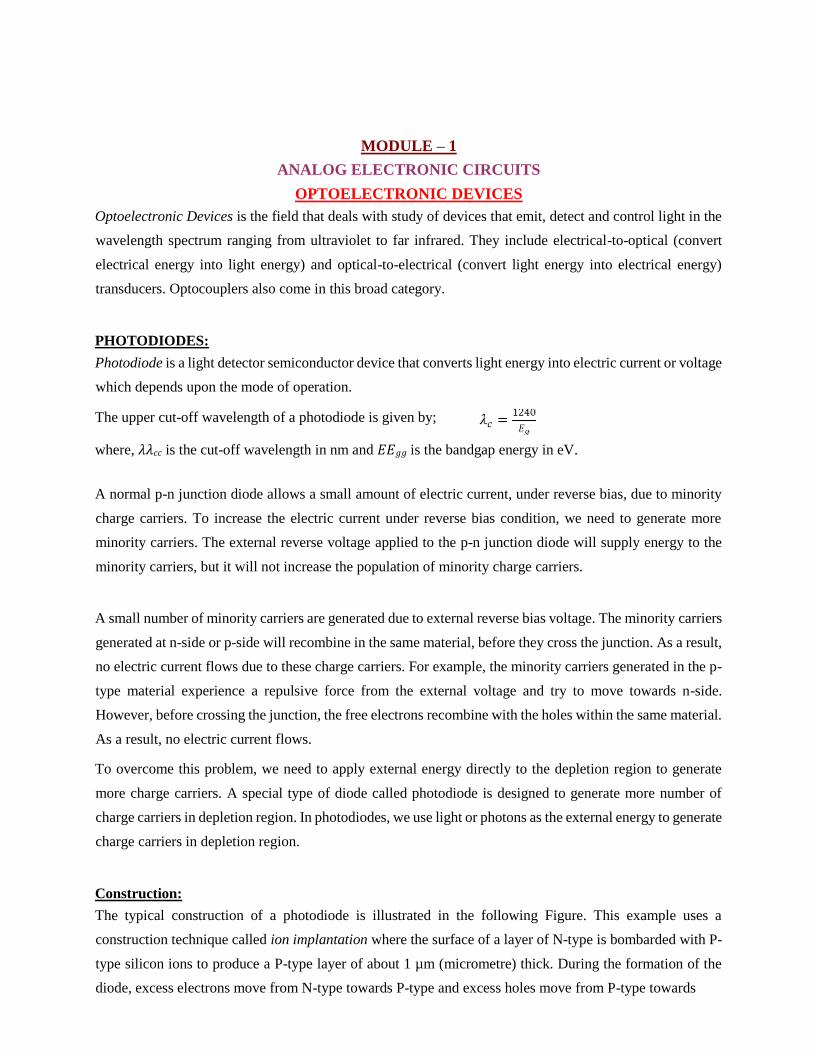
Construction:
The typical construction of a photodiode is illustrated in the following Figure. This example uses a
construction technique called ion implantation where the surface of a layer of N-type is bombarded with P-
type silicon ions to produce a P-type layer of about 1 µm (micrometre) thick. During the formation of the
diode, excess electrons move from N-type towards P-type and excess holes move from P-type towards
MAHESH PRASANNA K., VCET, PUTTUR

N-type; this process is called diffusion, resulting in the removal of free charge carriers close to the
PNjunction, so creating a depletion layer as shown in the following Figure.
The (light facing) top of the diode is protected by a layer of Silicon Dioxide (SiO2) in which there is a
window for light to shine on the semiconductor. This window is coated with a thin anti-reflective layer of
Silicon Nitride (SiN) to allow maximum absorption of light and an anode connection of aluminium (AI) is
provided to the P-type layer. Beneath the N-type layer, there is a more heavily doped N+ layer to provide a
low resistance connection to the cathode.
Working Principle:
When the conventional diode is reverse biased, the depletion region starts expanding and the current starts
flowing due to minority charge carriers. With the increase of reverse voltage, the reverse current also starts
increasing. The same condition can be obtained in photodiode without applying reverse voltage.
The following Figure shows photo diode bias symbol. The junction of Photodiode is illuminated by the light
source; the photons strike the junction surface. The photons impart their energy in the form of light to the
junction. Due to which electrons from valence band get the energy to jump into the conduction band. This
leaves positively charged holes in the valence band, so producing 'electron-hole pairs' in the depletion layer.
Some electron-hole pairs are also produced in P and N layers, but apart from those produced in the diffusion
region N layers, most will be re-absorbed within the P and N materials as heat. The electrons in the depletion
layer are then swept towards the positive potential on the cathode, and the holes swept towards the negative
potential on the anode, so creating a photo current. In this way, the photodiode converts light energy into
electrical energy.
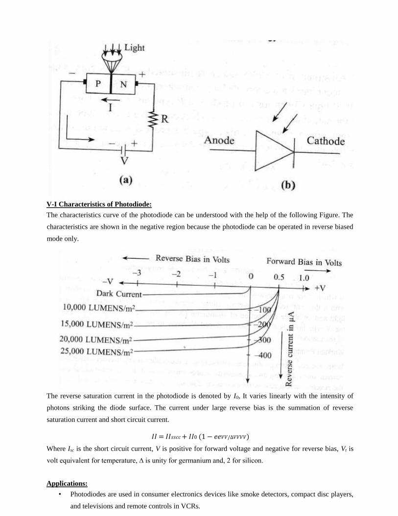
V-I Characteristics of Photodiode:
The characteristics curve of the photodiode can be understood with the help of the following Figure. The
characteristics are shown in the negative region because the photodiode can be operated in reverse biased
mode only.
The reverse saturation current in the photodiode is denoted by I0, It varies linearly with the intensity of
photons striking the diode surface. The current under large reverse bias is the summation of reverse
saturation current and short circuit current.
𝐼𝐼 = 𝐼𝐼𝑠𝑠𝑐𝑐 + 𝐼𝐼0 (1 − 𝑒𝑒𝑉𝑉/∆𝑉𝑉𝑉𝑉)
Where Isc is the short circuit current, V is positive for forward voltage and negative for reverse bias, Vt is
volt equivalent for temperature, ∆ is unity for germanium and, 2 for silicon.
Applications:
• Photodiodes are used in consumer electronics devices like smoke detectors, compact disc players,
and televisions and remote controls in VCRs.
• In other consumer devices like clock radios, camera light meters, and street lights, photoconductors
are more frequently used rather than photodiodes.
• Photodiodes are frequently used for exact measurement of the intensity of light in science and
industry. Generally, they have an enhanced, more linear response than photoconductors.
LIGHT EMITTING DIODE (LED):
The LED is a PN-junction diode which emits light when an electric current passes through it in the forward
direction. A P-N junction can convert absorbed light energy into a proportional electric current. The same
process is reversed here (i.e. the P-N junction emits light when electrical energy is applied to it). This
phenomenon is generally called Electroluminescence.
Electroluminescence is the properly of the material to convert electrical energy into light energy and later
it radiates this light energy. Different sizes of light emitting diodes are available in market form lmm2 to
onward.
Construction:
The semiconductor material used in LED is Galliurn Arsenide (GaAs), Gallium phosphide (GaP) or Gallium
Arsenide Phosphide (GaAsP). Any of the above-mentioned compounds can be used for the construction of
LED, but the color of radiated light changes with the change in material (for example, GaP material gives
green/red color with forward voltage of 2.2V).
The semiconductor layer of P-type is placed above N-type because the charge carrier recombination occurs
in P-type. Besides, it is the surface of the device, and thus, the light emitted can be easily seen on the surface.
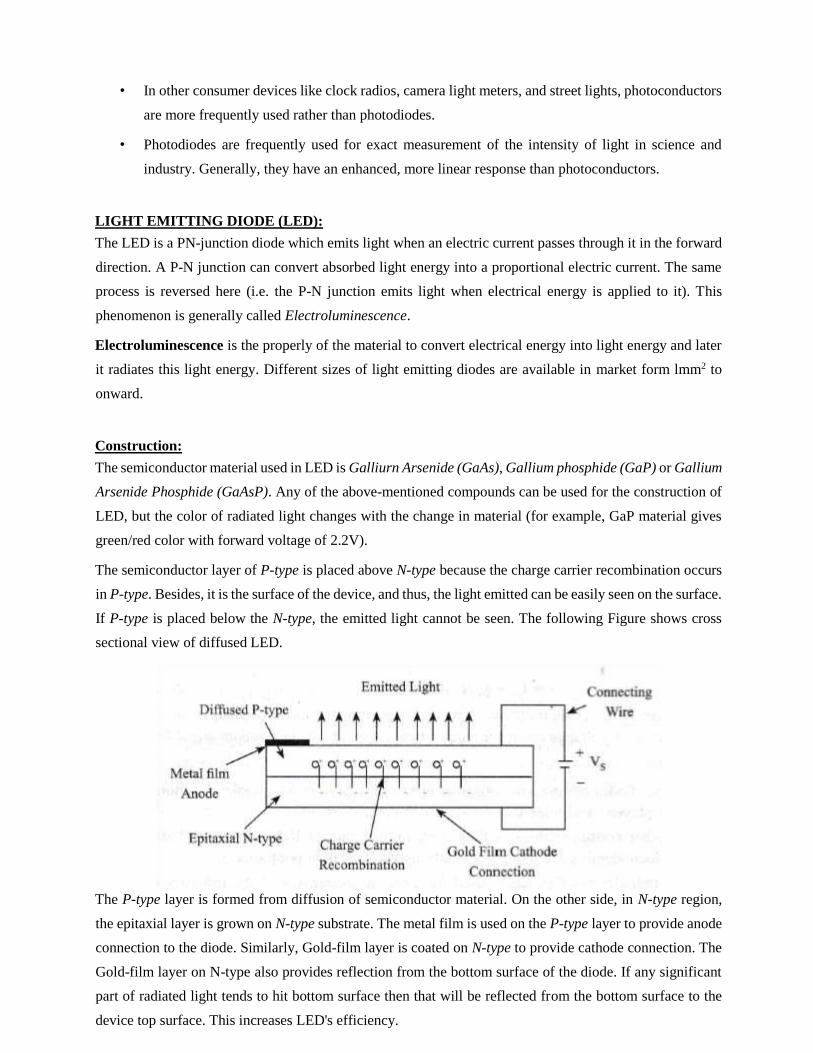
If P-type is placed below the N-type, the emitted light cannot be seen. The following Figure shows cross
sectional view of diffused LED.
The P-type layer is formed from diffusion of semiconductor material. On the other side, in N-type region,
the epitaxial layer is grown on N-type substrate. The metal film is used on the P-type layer to provide anode
connection to the diode. Similarly, Gold-film layer is coated on N-type to provide cathode connection. The
Gold-film layer on N-type also provides reflection from the bottom surface of the diode. If any significant
part of radiated light tends to hit bottom surface then that will be reflected from the bottom surface to the
device top surface. This increases LED's efficiency.
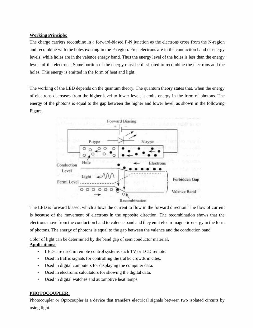
Working Principle:
The charge carriers recombine in a forward-biased P-N junction as the electrons cross from the N-region
and recombine with the holes existing in the P-region. Free electrons are in the conduction band of energy
levels, while holes are in the valence energy band. Thus the energy level of the holes is less than the energy
levels of the electrons. Some portion of the energy must be dissipated to recombine the electrons and the
holes. This energy is emitted in the form of heat and light.
The working of the LED depends on the quantum theory. The quantum theory states that, when the energy
of electrons decreases from the higher level to lower level, it emits energy in the form of photons. The
energy of the photons is equal to the gap between the higher and lower level, as shown in the following
Figure.
The LED is forward biased, which allows the current to flow in the forward direction. The flow of current
is because of the movement of electrons in the opposite direction. The recombination shows that the
electrons move from the conduction band to valence band and they emit electromagnetic energy in the form
of photons. The energy of photons is equal to the gap between the valence and the conduction band.
Color of light can be determined by the band gap of semiconductor material.
Applications:
• LEDs are used in remote control systems such TV or LCD remote.
• Used in traffic signals for controlling the traffic crowds in cites.
• Used in digital computers for displaying the computer data.
• Used in electronic calculators for showing the digital data.
• Used in digital watches and automotive heat lamps.
PHOTOCOUPLER:
Photocoupler or Optocoupler is a device that transfers electrical signals between two isolated circuits by
using light.
Photocouplers are used in many functions: they can be used to link data across two circuits; they can be used
within optical encoders, where the optocoupler provides a means of detecting visible edge transitions on an
encoder wheel to detect position, etc., and they can be used in many other circuits where optical links and
transitions are needed. As a result, optical couplers or photocouplers are found in many circuits.
Construction:
All optocouplers consist of two elements: a light source (a LED) and a photosensor (a photoresistor,
photodiode, phototransistor, silicon-controlled rectifier (SCR), or triac); which are separated by a dielectric
(non-conducting) barrier.
Working Principle:
When input current is applied to the LED, it switches ON and emits infrared light; the photosensor then
detects this light and allows current to flow through the output side of the circuit; conversely, when the LED
is off, no current will flow through the photosensor. By this method, the two flowing currents are electrically
isolated. It consists of LED and photodiode; where the circuits are isolated electrically. In the following
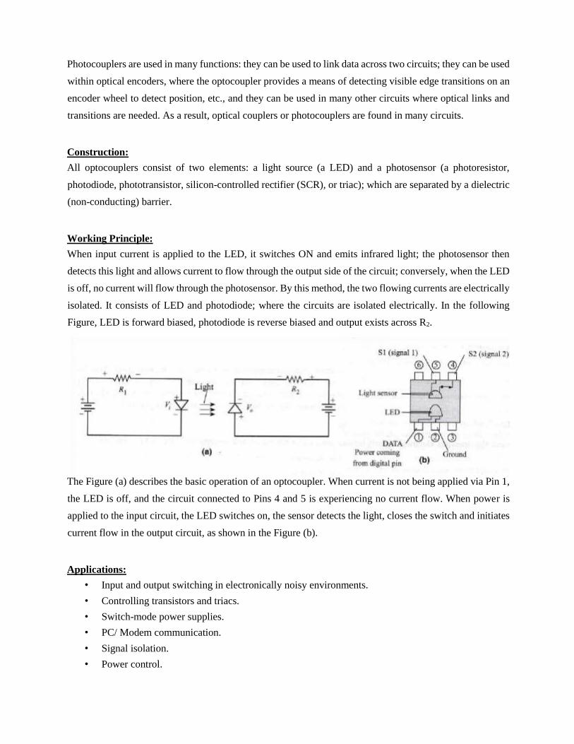
Figure, LED is forward biased, photodiode is reverse biased and output exists across R2.
The Figure (a) describes the basic operation of an optocoupler. When current is not being applied via Pin 1,
the LED is off, and the circuit connected to Pins 4 and 5 is experiencing no current flow. When power is
applied to the input circuit, the LED switches on, the sensor detects the light, closes the switch and initiates
current flow in the output circuit, as shown in the Figure (b).
Applications:
• Input and output switching in electronically noisy environments.
• Controlling transistors and triacs.
• Switch-mode power supplies.
• PC/ Modem communication.
• Signal isolation.
• Power control.

MULTIVIBRATORS USING IC-555
A multivibrator (like an oscillator) is a circuit with regenerative feedback, which produces a pulsed output.
There are three basic types of multivibrator circuits:
• Astable – has no stable states, but switches continuously between two states. This action produces
a train of square wave pulses at a fixed frequency.
• Monostable – one of the states is stable, but the other state is unstable (transient).
• Bistable – the circuit is stable in either state.
Timer IC-555:
Timer IC-555 is the one of the most commonly used general-purpose linear integrated circuits.
Internal Schematic of Timer IC-555
The Timer IC 555 comprises two Op-Amp comparators, a flip-flop, a discharge transistor, a reset transistor,
three identical resistors and an output stage. The resistors set the reference voltage levels at the non-inverting
input of the lower comparator and inverting input of the upper comparator at +VCC/3 and 2VCC/3,
respectively. The output of two comparator feed SET and RESET inputs of the Flip-Flop. This decided the
logic state of its output and subsequently the final output. The Flip-Flops complementary outputs feed the
output stage and the base of the discharge transistor. Hence, when the output is HIGH, the discharge
transistor is OFF and when the output is LOW, the discharge transistor is ON.
MAHESH PRASANNA K., VCET, PUT
12
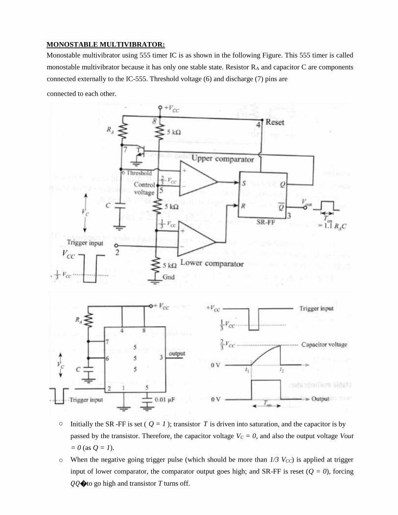
MONOSTABLE MULTIVIBRATOR:
Monostable multivibrator using 555 timer IC is as shown in the following Figure. This 555 timer is called
monostable multivibrator because it has only one stable state. Resistor RA and capacitor C are components
connected externally to the IC-555. Threshold voltage (6) and discharge (7) pins are
passed by the transistor. Therefore, the capacitor voltage VC = 0, and also the output voltage Vout
= 0 (as Q = 1).
o When the negative going trigger pulse (which should be more than 1/3 VCC) is applied at trigger
input of lower comparator, the comparator output goes high; and SR-FF is reset (Q = 0), forcing
𝑄𝑄 to go high and transistor T turns off.
connected to each other.
o Initially the SR - FF is set ( Q = 1 ) ; transistor T is driven into saturation, and the capacitor is by

o As T is off, capacitor starts charging through RA. Now, the output will remain high (from t1 to t2, in
waveform shown).
o At time t2; the voltage across the capacitor VCC becomes more than 2/3 VCC and upper comparator
output goes high. This will set the SR-FF (Q = 1).
o Since, SR-FF output Q = 1; transistor T is ON, and hence, capacitor discharges, and also output
goes low. The output remains low till the next trigger pulse is applied.
From the waveform of monostable multivibrator, it is clear that, the ON time TON of the output voltage is
same as charging time of the capacitor.
Therefore, TON → is the time taken by capacitor to charge from 0 to 2/3 VCC.
The voltage across capacitor increases exponentially and is given by;
As capacitor charges through RA; let us replace R by RA: Hence,
At t = t2 (TON), the capacitor voltage (VC) reaches 2/3 VCC:
𝑇𝑇𝑂𝑂𝑂𝑂
Therefore, Or, = 1 – 2/3 = 1/3
Therefore, TON = 1.1 RAC
Applications:
A monostable multivibrator can be used in many applications, few important applications are
1. Frequency divider
2. Missing pulse detector 3.
Pulse width modulator
4. Pulse position modulator etc.

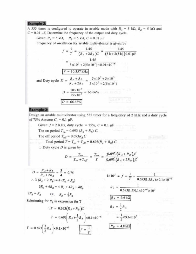
ASTABLE MULTIVIBRATOR:

An astable multivibrator does not have any stable state; it keeps changing its state from low to high and
high to low. This multivibrator is also called free running multivibrator or rectangular wave generator
circuit. Astable multivibrator does not require an external trigger pulse to change the state of the output.
ON time operation:
o At t = 0, the voltage on the capacitor VCC = 0, the same capacitor voltage is applied to both trigger
point of lower comparator and threshold point of upper comparator. As capacitor voltage VC = 0,
which is less 1/3 VCC, the output of lower comparator goes high (𝑄𝑄 = l) and Q = 0. This causes
T to go off and capacitor starts charging through series resistors RA and RB. When capacitor voltages
reaches 2/3 VCC, on time is terminated.
OFF time operation:
o As soon as VC exceeds 2/3 VCC, the upper comparator output goes high and it will set the SR FF.
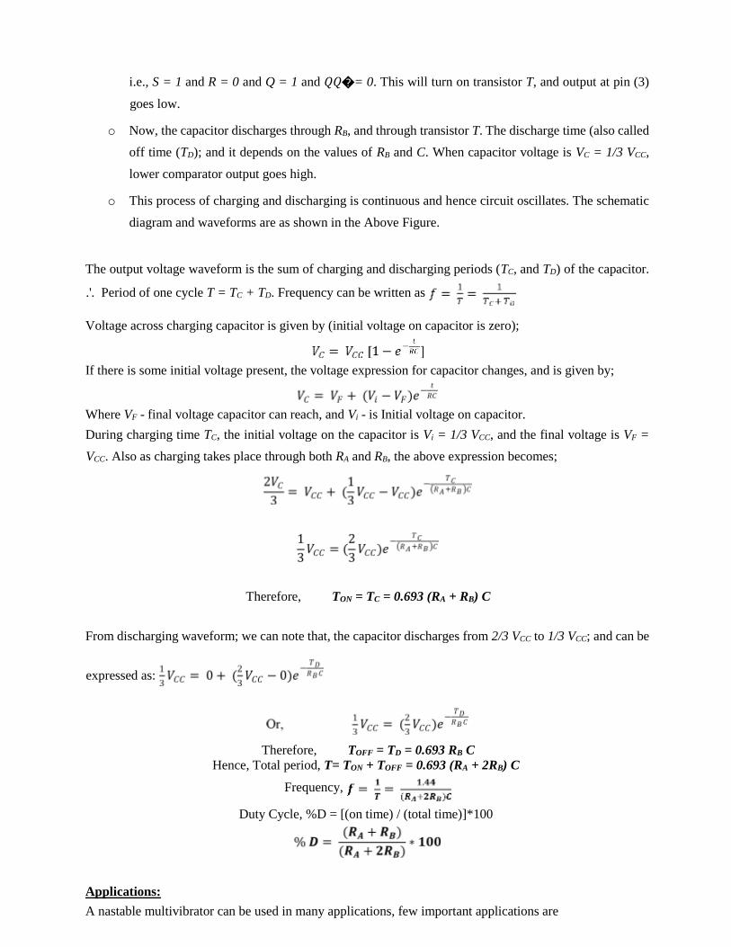
The circuit con f iguration of an astable rnultivibrator is as shown in the following Figure.
To understand the operation, let us divide the circuit operation into two time interval T ON and T OFF .
i.e., S = 1 and R = 0 and Q = 1 and 𝑄𝑄 = 0. This will turn on transistor T, and output at pin (3)
goes low.
o Now, the capacitor discharges through RB, and through transistor T. The discharge time (also called
off time (TD); and it depends on the values of RB and C. When capacitor voltage is VC = 1/3 VCC,
lower comparator output goes high.
o This process of charging and discharging is continuous and hence circuit oscillates. The schematic
diagram and waveforms are as shown in the Above Figure.
The output voltage waveform is the sum of charging and discharging periods (TC, and TD) of the capacitor.
.'. Period of one cycle T = TC + TD. Frequency can be written as
Voltage across charging capacitor is given by (initial voltage on capacitor is zero);
If there is some initial voltage present, the voltage expression for capacitor changes, and is given by;
Where VF - final voltage capacitor can reach, and Vi - is Initial voltage on capacitor.
During charging time TC, the initial voltage on the capacitor is Vi = 1/3 VCC, and the final voltage is VF =
VCC. Also as charging takes place through both RA and RB, the above expression becomes;
Therefore, TON = TC = 0.693 (RA + RB) C
From discharging waveform; we can note that, the capacitor discharges from 2/3 VCC to 1/3 VCC; and can be
expressed as:
Therefore, TOFF = TD = 0.693 RB C
Hence, Total period, T= TON + TOFF = 0.693 (RA + 2RB) C
Frequency,
Duty Cycle, %D = [(on time) / (total time)]*100
Applications:
A nastable multivibrator can be used in many applications, few important applications are
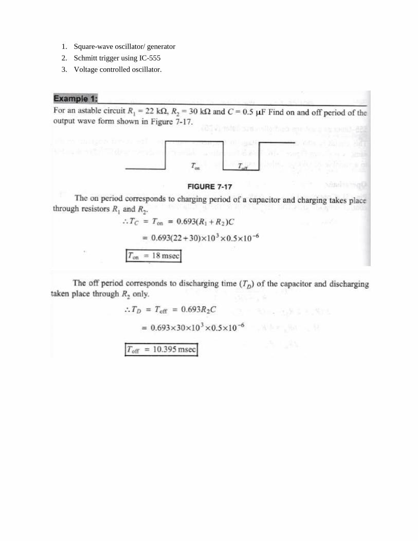
1. Square-wave oscillator/ generator
2. Schmitt trigger using IC-555
3. Voltage controlled oscillator.

OPERATIONAL AMPLIFIER (OP-AMP) APPLIATION CIRCUITS
An Op-Amp is a direct-coupled high gain, high bandwidth differential amplifier with very high value of
input impedance and very low value of output impedance.
Basic Differential Amplifier & Circuit Representation of an OP-Amp
The ideal Op-Amp model was derived to simplify circuit calculations. The ideal Op-Amp model makes three
assumptions:
Ideal Op-Amp Practical Op-Amp 1. Input resistance (impedance), Ri = ∞ Internal Impedance is infinite Input Impedance range 100KΩ to
2. Output resistance (impedance), Ro = 0 1000MΩ
3. Open-loop (differential voltage) gain, Ad = ∞ Output Impendence is zero Output impedance range from 10Ω
Based on these three assumptions, to 100Ω Open loop differential voltage gain is Open loop gain is in the range of
other assumptions can be derived: infinite 10,000 to 100,000
1. Since Ri = ∞, Ii = Ini = 0 Bandwidth is infinite Bandwidth is limited
2. Since Ro = 0, Vo = Ad * Vd DC input and output offset voltage is Finite DC input and output offset zero voltage
3. Zero DC input and output offset voltages Input differential voltage is zero Finite differential voltage is finite
4. Bandwidth and slew rate are also infinite, as no frequency dependencies are assumed.
5. Drift is also zero, as there is no changes in performance over time, temperature, power supply variations, and so
on
6. Since output voltage depends only on differential input voltage, it rejects any voltage common to both inputs.
Hence, common mode gain = 0
Open-loop gain is the differential voltage gain in the absence of any positive or negative feedback. Practical OpAmps
have –
1. Input impedance can vary from hundred of kilo-ohms (for some low-grade Op-Amps) to tera-ohms (for high
grade Op-Amps).
2. Output impedance may be in the range of 10 to 100 Ω
3. Open-loop gain in the range of 10,000 to 1, 00,000
4. Bandwidth is limited and is specified by gain-bandwidth product
5. There may be some finite DC output (referred to as output offset voltage), even when both the inputs are
grounded.
PEAK DETECTORS:

Peak detector detects holds the most positive value attained by the input signal. The following Figure shows
peak detector circuit.
During positive half cycle of the input, D-conducts and capacitor charges to peak (highest) value of the
input. Capacitor retains its charged value unless and until it discharges with a help of switch.
The op-amp is connected as a voltage follower and its output voltage will be equal the drop across
capacitor which is positive peak value of the applied voltage and will remain that for long periods until next
more higher peak occurs at the input. For negative cycle of input, the diode is reverse biased and capacitor
retains its value.
Modified Peak Detector:
More sophisticated peak detector that buffers the signal source from the capacitor is shown in the following
Figure.
As Op-Amp (A1) is connected as voltage follower, the circuit presents very high impedance to the signal
source. Op-Amp (A2) acts as a buffer between the capacitor and the load. Output (V0) at any given time is
equal to the voltage on the capacitor which is nothing but, the peak value of the input occurred up to that
time.
Whenever the input signal has higher peak than the present one, the capacitor charges up to new
high input level. Whenever input level gets dropped, then capacitor retains the peak value of input, as diode
D1 gets reverse biased and diode D2 prevents amplifier A1 output from going into negative saturation.
To hold the negative peak of the input signal, reverse the diode connections in the above Figure.
Applications:
o Used for AM in communication o Used in test and
measurement instrumentation applications.
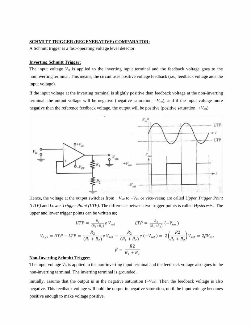
SCHMITT TRIGGER (REGENERATIVE) COMPARATOR:
A Schmitt trigger is a fast-operating voltage level detector.
Inverting Schmitt Trigger:
The input voltage Vin is applied to the inverting input terminal and the feedback voltage goes to the
noninverting terminal. This means, the circuit uses positive voltage feedback (i.e., feedback voltage aids the
input voltage).
If the input voltage at the inverting terminal is slightly positive than feedback voltage at the non-inverting
terminal, the output voltage will be negative (negative saturation, –Vsat); and if the input voltage more
negative than the reference feedback voltage, the output will be positive (positive saturation, +Vsat).
Hence, the voltage at the output switches from +Vsat to –Vsat or vice-versa; are called Upper Trigger Point
(UTP) and Lower Trigger Point (LTP). The difference between two trigger points is called Hysteresis. The
upper and lower trigger points can be written as;
Non-Inverting Schmitt Trigger:
The input voltage Vin is applied to the non-inverting input terminal and the feedback voltage also goes to the
non-inverting terminal. The inverting terminal is grounded..
Initially, assume that the output is in the negative saturation (–Vsat). Then the feedback voltage is also
negative. This feedback voltage will hold the output in negative saturation, until the input voltage becomes
positive enough to make voltage positive.
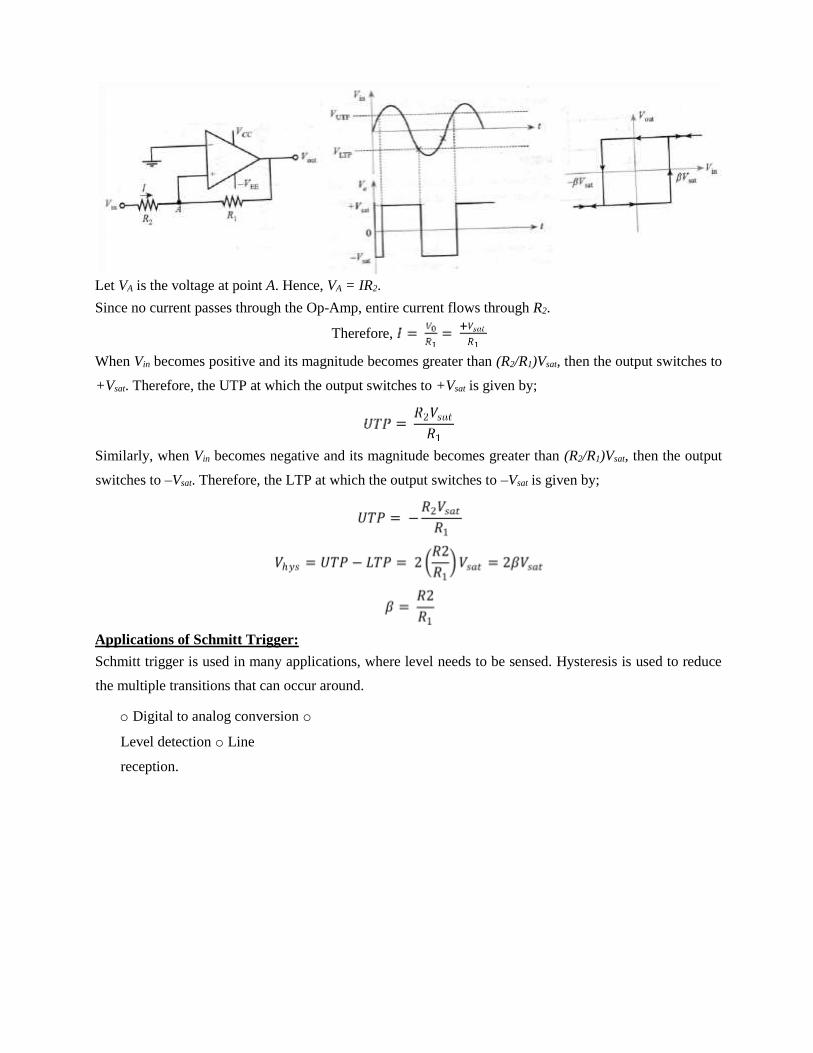
Let VA is the voltage at point A. Hence, VA = IR2.
Since no current passes through the Op-Amp, entire current flows through R2.
Therefore,
When Vin becomes positive and its magnitude becomes greater than (R2/R1)Vsat, then the output switches to
+Vsat. Therefore, the UTP at which the output switches to +Vsat is given by;
Similarly, when Vin becomes negative and its magnitude becomes greater than (R2/R1)Vsat, then the output
switches to –Vsat. Therefore, the LTP at which the output switches to –Vsat is given by;
Applications of Schmitt Trigger:
Schmitt trigger is used in many applications, where level needs to be sensed. Hysteresis is used to reduce
the multiple transitions that can occur around.
o Digital to analog conversion o
Level detection o Line
reception.


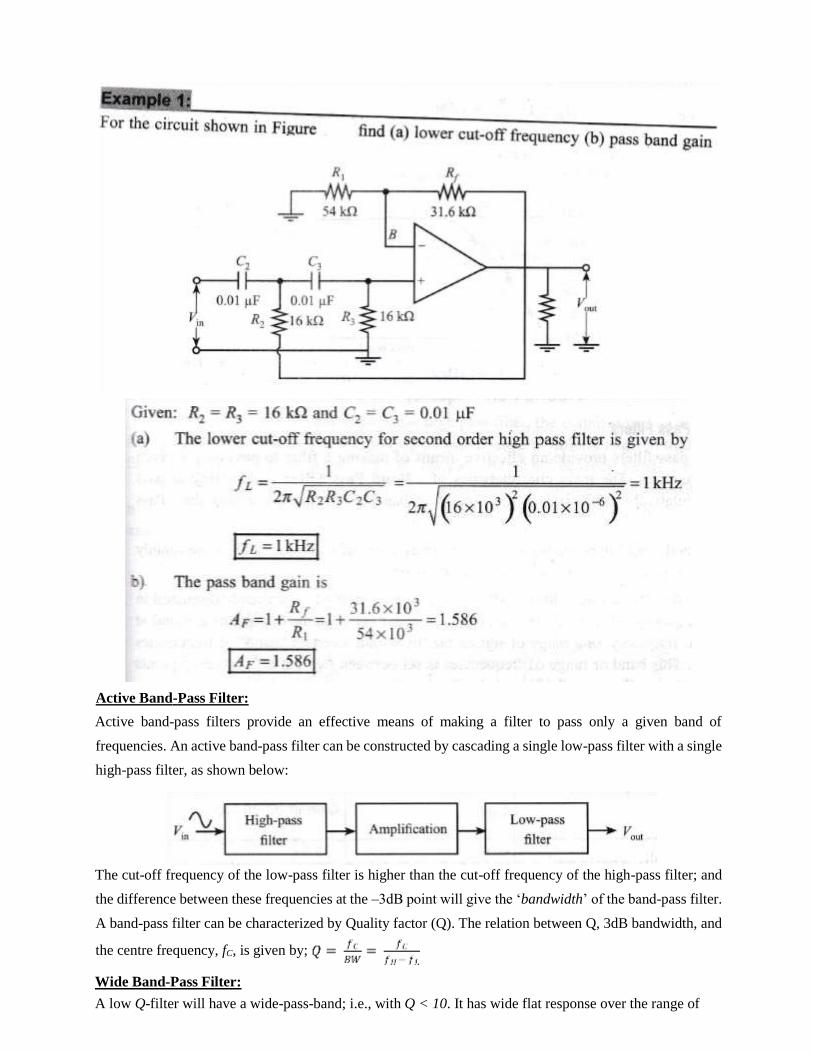
ACTIVE FILTERS:

Filter is a frequency selective circuit commonly used in signal processing that passes signal of specified
range of frequencies and blocks the signals of frequencies outside the band. Active filters are attractive due
to their –
• Flexibility in gain control
• Small component size
• No loading Problem
• Pass band gain
• Use of the inductors can be avoided
Filters are useful in many areas of applications, such as Communication and Signal Processing. They are
found in electronic systems like Radio, Television, Telephones, Radars, satellites, and Biomedical
instruments.
Broader Classification of Filters
Passive filters work for high frequencies; but at audio frequencies, the inductors become problematic, as
they are large, heavy, high power dissipation, and expensive.
Active filters use Op-Amp as the active element, resistors and capacitors as passive elements.
SNo. Passive Filters Active Filters
1 Filters with only components like resistors,
capacitors, and inductors are known as
passive filters.
Filters with components such as Op-Amps,
transistors, and other active elements are known as
active filters.
2 Passive filters do not require an external
power source for operation; incapable of
providing power gain.
Active filters require an external power supply for
operation; capable of providing power gain.
3 Better stability and can withstand large
currents.
Oscillations and noise will be generated due to
feedback loops.
4 A passive filter has no frequency Due to active elements, active filters have
limitations. frequency limitations.
Filters
Digital Filters Analog Filters
Passive Filters Active Filters

5 Passive filters circuits are bulky/ heavy due
to the presence of inductors; they consume
more power and operate with limited
speed.
Active filters circuits are more compact, less
heavy; and operate with high speed.
6 Difficult to fabricate in IC form and usually
designed using discrete components.
Can be fabricated in IC form and usually designed
using discrete components.
Active filters offer the following advantages over Passive filters:
• Gain and frequency adjustment flexibility
• No loading problem & No insertion loss
• Size and weight
• Cost.
Most commonly used active filters are –
• Low-pass filter, High-pass filter, Band-pass filter, Band-stop filter (Band-reject filter), and Allpass
filter.
Design:
An active filter generally uses Op-Amp. Op-Amp has very high input impedance and low output impedance.
The gain is determined by the resistive network in the feedback loop.
First Oder Active Low-Pass Filter (LPF):
Frequency Response:

The first-order low-pass butter worth filter consists of a single RC filter stage, providing a low frequency
path to the non-inverting input of an Op-Amp. The circuit diagram and the frequency response of the
• At cut-off frequency, f = fH, the gain is 0.707AF.
• After cut-off frequency fH, the gain decreases at the rate of 20 dB/decade.
• The cut-off frequency is given by:
• Pass band gain is given by:
Some applications of low-pass filters are – o Low-pass filters are used in Audio
amplifiers o LPFs are used in equalizers or speakers to reduce the high
frequency noise.
circuit is given below:
• From the graph; the gain ( A F ) is almost constant for the frequency range: 0 < f < f H .

First order filter can be converted to second order filter by adding an extra RC-network, as shown in the
following Figure. The frequency response of second order low-pass filter is same as the first order lowpass
filter except that the gain at the stop band rolls off at the rate of 40 dB/decade.
• After cut-off frequency fH, the gain decreases at the rate of 40 dB/decade.
Second Order Low - Pass Filter:

• The cut-off frequency is given by: . o If R2 = R3 = R & C2 = C3 = C; then
• Pass band gain is given by:

High-Pass Butter Worth Filter:
High-pass filters passes higher frequency signals, attenuating all signals below cut-off frequency, fL.
First Order High-Pass Butter Worth Filter:
The filter circuit consists of a passive filter followed by a non-inverting amplifier.
• At low frequency: f < fL, < AF. AF increases at the rate of 20 dB/decade till f = fL.
• At cut-off frequency, f = fL, the gain is 0.707AF.
• At very high frequency f > fL, = AF is constant.
• The cut-off frequency is given by:
• Pass band gain is given by:

Second Order High-Pass Filter:
A first order high-pass filter can be converted into a second order high-pass filter by using an extra
RCnetwork in the input side. The frequency response of second order high-pass filter is same as the first
order high-pass filter except that the gain at the stop band rolls off at the rate of 40 dB/decade.
• The cut-off frequency is given by: .
o If R2 = R3 = R & C2 = C3 = C; then
• Pass band gain is given by:
Active band-pass filters provide an effective means of making a filter to pass only a given band of
frequencies. An active band-pass filter can be constructed by cascading a single low-pass filter with a single
high-pass filter, as shown below:
The cut-off frequency of the low-pass filter is higher than the cut-off frequency of the high-pass filter; and
the difference between these frequencies at the –3dB point will give the ‘bandwidth’ of the band-pass filter.
A band-pass filter can be characterized by Quality factor (Q). The relation between Q, 3dB bandwidth, and
the centre frequency, fC, is given by;
Wide Band-Pass Filter:
A low Q-filter will have a wide-pass-band; i.e., with Q < 10. It has wide flat response over the range of
Active Band - Pass Filter:

A high Q-filter will have a narrow-pass-band; i.e., with Q > 10. It has a sharp bell type response, with high
gain and high selectivity.
• .
•
• Maximum Gain,
frequencies and bandwidth is large.
Narrow Band - Pass Filter:

Applications of Band-Pass Filters (BPF):
o BPFs are also used in optics like Lasers, LIDARS, etc. o BPFs are extensively used in wireless
transmitters and receivers.
o BPFs are used in electronic devices like Sonar, Seismology; and medical applications like ECG,
and electrocardiograms.
o BPFs are extensively used for Audio signal processing, where a particular range of frequencies of
sound is required while removing the rest.
Band-Stop Filter (Band-Reject Filter):
Band-Stop Filer (BSF) is another type of frequency selective circuit that functions in exactly opposite to the
band-pass filter. BSF passes all frequencies with the exception of those within a specified stop band, which
are attenuated. If this stop band is very narrow and highly attenuated over a few hertz, then the band-stop
filter is referred as a notch filter.
Wide Band-Reject Filter:
The frequency response curve and the circuit diagram of a wide band-reject filter is given below.
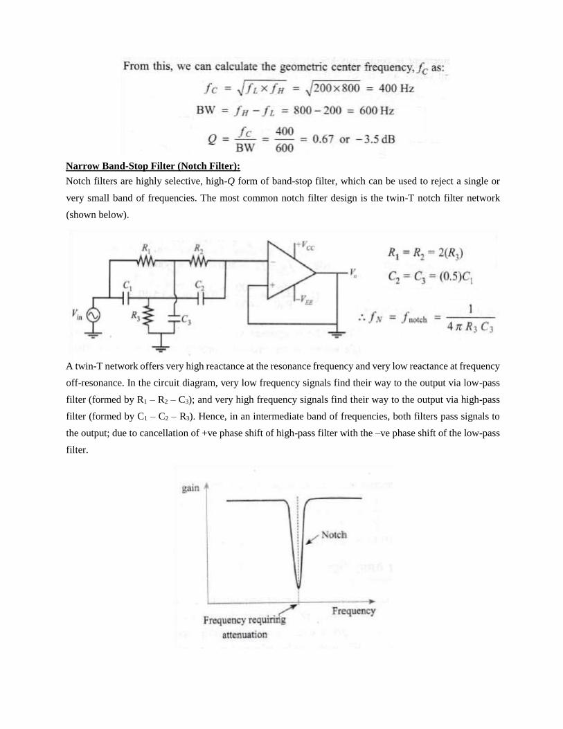
Narrow Band-Stop Filter (Notch Filter):
Notch filters are highly selective, high-Q form of band-stop filter, which can be used to reject a single or
very small band of frequencies. The most common notch filter design is the twin-T notch filter network
(shown below).
A twin-T network offers very high reactance at the resonance frequency and very low reactance at frequency
off-resonance. In the circuit diagram, very low frequency signals find their way to the output via low-pass
filter (formed by R1 – R2 – C3); and very high frequency signals find their way to the output via high-pass
filter (formed by C1 – C2 – R3). Hence, in an intermediate band of frequencies, both filters pass signals to
the output; due to cancellation of +ve phase shift of high-pass filter with the –ve phase shift of the low-pass
filter.

NON LINEAR AMPLIFIER:
Non linearity is the behavior of a circuit, particularly an amplifier, in which the output signal strength do not
vary in direct proportion to the input signal strength. A non-linear amplifier in as circuit which gives non
linear relationship between its input and output signals.
The Non linear amplification can be achieved in a simple way by just connecting a non-linear device such
as PN-junction diode in the feedback path. In the circuit shown is the following Figure, large change in input
voltage causes small change in the output voltage. This circuit is a log amplifier, hence the output voltage
is logarithm of the input voltage.
The above Figure shows a non-linear amplifier, where diode ‘D’ is used in negative feedback path. By virtual
ground concept; as node B is grounded, node A will be virtually grounded. Therefore, VA = 0.
MAHESH PRASANNA K., VCET, PUTTUR
We have; since VA = 0.

Let If be the current through the diode. The voltage across diode is VA – V0. Since, VA = 0, the voltage across
diode is –V0.
Diode equation:
Where, VT – Voltage equivalent of Temperature
If – Diode forward current Ir –
Diode reverse saturation current.
Since, current through the Op-Amp is negligible;I = If
Therefore, If
Gives, IrR = Vref is a constant.
The above equation shows that, the output voltage is a logarithmic function of input voltage.
Applications: Non-linear Amplifiers are used in AC bridge balance detectors.
RELAXATION OSCILLATOR:
Relaxation oscillator is a non-linear electronic oscillator circuit that generates a continuous non-sinusoidal
output signal in the form of rectangular wave, triangular wave or a saw-tooth wave. The time period of non-
sinusoidal output depends on the charging time of the capacitor connected in the oscillator circuit. The
relaxation oscillator basically contains a feedback loop that has a switching device in the form of transistor,
relays, operational amplifiers, comparators, or a tunnel diode that charges a capacitor through a resistance
till it reaches a threshold level then discharges it again. The following Figure shows the basic circuit of an
Op-Amp based relaxation oscillator.
Assume that, the output is initially in positive saturation. As a result, voltage at non-inverting input of
OpAmp is +VSAT * R1 / (R1 + R2). This force the output to stay in positive saturation as the capacitor C is
initially in fully discharged state. Capacitor C starts charging towards +VSAT through R. The moment the
capacitor voltage exceeds the voltage appearing at the non-inverting input, the output switches to –VSAT.
Now, the voltage appearing at the non-inverting input changes to –VSAT * R1 / (R1 + R2). The
capacitor starts discharging and after reaching zero, it begins to discharge towards –VSAT. Again, as soon as

it becomes more negative than the voltage appearing at the non-inverting input of the Op-Amp, the output
switches back to +VSAT.
The expression for the time period of the output rectangular waveform is given by;
In the above equation; the natural logarithm is used, which is logarithm to base e. By varying the value of
resistor R, the time period of the output waveform can be varied.
β is the feedback fraction/ factor and is given by β = R1/ (R1+R2)
When the output voltage V0 is at at +VSAT the feedback voltage is known as upper threshold voltage VUTP
and is given by +VSAT x R1/ (R1+ R2)
When the output voltage V0 is at at –VSAT the feedback voltage is known as lower threshold voltage VLTP
and is given by –VSAT x R1/ (R1+ R2)
VOLTAGE TO CURRENT (V TO I) CONVERTER:
In many applications, we have to convert a voltage to a proportionate current. These voltage-to-current
converter circuits can be of two types:
a) Voltage to Current Converter with Floating Load: The circuit is shown in the following
Figure, where RL is the floating load.
Since, voltage at node A is Vi; 𝑉𝑉𝑖𝑖 = 𝐼𝐼𝐿𝐿𝑅𝑅1 Or,
i.e., input voltage Vi is converted into and output current.
b) Voltage to Current Converter with Grounded Load: The circuit is shown in the following
Figure.
The load current is given by; IL = I1 + I2
Therefore,
For a non-inverting amplifier, we know that;
Therefore,
Thus, the current IL is proportionate to voltage.
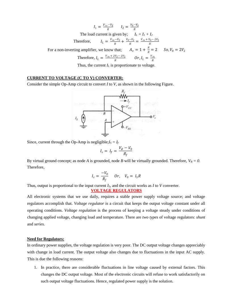
CURRENT TO VOLTAGE (C TO V) CONVERTER:
Consider the simple Op-Amp circuit to convert I to V, as shown in the following Figure.
Since, current through the Op-Amp is negligible;IS = If
By virtual ground concept; as node A is grounded, node B will be virtually grounded. Therefore, VB = 0.
Therefore,
Thus, output is proportional to the input current IS, and the circuit works as I to V converter.
VOLTAGE REGULATORS
All electronic systems that we use daily, requires a stable power supply voltage source; and voltage
regulators accomplish that. Voltage regulator is a circuit that keeps the output voltage constant under all
operating conditions. Voltage regulation is the process of keeping a voltage steady under conditions of
changing applied voltage, changing load and temperature. There are two types of voltage regulators: shunt
and series.
Need for Regulators:
In ordinary power supplies, the voltage regulation is very poor. The DC output voltage changes appreciably
with change in load current. The output voltage also changes due to fluctuations in the input AC supply.
This is due the following reasons:
1. In practice, there are considerable fluctuations in line voltage caused by external factors. This
changes the DC output voltage. Most of the electronic circuits will refuse to work satisfactorily on
such output voltage fluctuations. Hence, regulated power supply is the solution.

2. The internal resistance of ordinary power supply is relatively large ( > 30 Ω). Therefore, output
voltage is affected by the amount of load current drawn from the supply. These variations in DC
voltage may cause erratic operation of circuits. Without stable potentials, circuit performance
degrades and if the variations are large enough, the components may get destroyed. In order to avoid
this, regulated power supply is used.
Input to the voltage regulator is unregulated pulsating DC obtained from filter rectifier. Its output is constant
DC voltage which is almost ripple free. The following Figure shows block diagram of regulated power
supply.
The transformer provides voltage transformation and electrical isolation between the input power supply
(AC mains) and the DC output. The rectifier circuit changes the AC voltage appearing across the transformer
secondary to DC (unidirectional output). The rectifier circuit always has some AC content known as ripple.
The filter circuit smoothens the ripple of the rectifier circuit. The regulator is a type of feedback circuit that
ensures that the output DC voltage does not change from its nominal value due to change in line voltage or
load current.
Factors Affecting the Load Voltage:
The variables affecting the load voltage in a power supply are given below:
1. Load current (IL): Ideally the output voltage should remain constant in-spite of changes in the load
current, but practically the power supply without regulator, the load voltage decreases as load
current, IL, increases. For practical power supply regulator, the load voltage must be constant
through load to full load condition.
2. Line voltage: The input to the rectifier is AC (230 V) is the line voltage. This input decides the
output voltage level. If input changes, output also changes. So this affects the performance of power
supply. So ideally voltage must remain constant irrespective of any changes in the line voltage.
3. Temperature: In the power supply, the rectifier unit is used which uses PN-junction diode. As the
diode characteristics are temperature dependent, the overall performance of the power supply is
temperature dependent.
Performance Parameters of a Power Supply:
The power supply is judged by some parameters, called as performance parameters. These performance
parameters are explained below:

1. Line Regulation: If the input to the rectifier unit i.e. 230 V changes, the output DC of rectifier will
also change and since the output of rectifier is applied to the regulator, the output of regulator will
also vary. Thus the source causes the change in output. This is as source regulation or line
regulation. It is defined as the change in regulated DC output for a given change in input (line)
voltage. Ideally the source regulation should be zero and practically it should be as low as possible.
2. Load Regulation: Load regulation is defined as the change in the regulated output voltage when
load current is changed from zero (no load) to maximum value (full load). The load regulation
ideally should be zero, but practically it should be as small as possible. The following Figure shows
the load regulation characteristics. Percentage load regulation =

39
Example: A regulated power supply provides a ripple rejection of –80dB. If the ripple voltage in the
unregulated input were 2V, determine the output ripple.
Ripple rejection in dB is given by; = –80dB
Or = –4
Or = 10–4
Therefore, output ripple = 2 * 10–4 V = 0.2mV
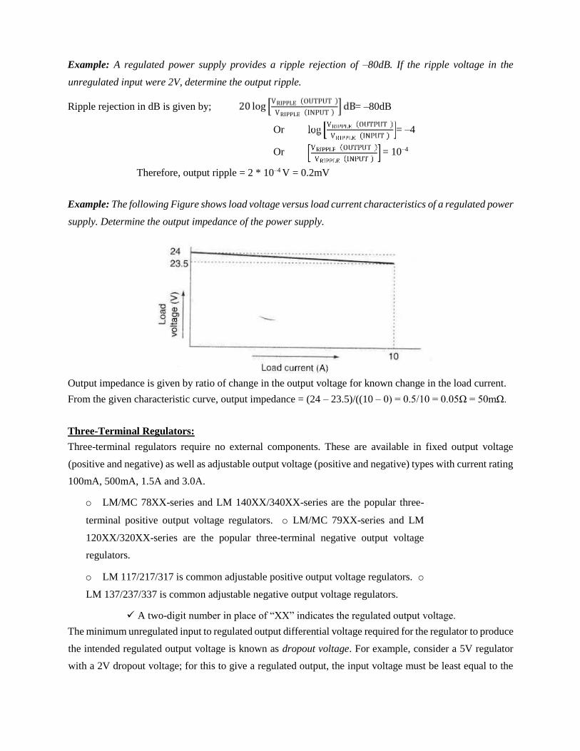
Example: The following Figure shows load voltage versus load current characteristics of a regulated power
supply. Determine the output impedance of the power supply.
Output impedance is given by ratio of change in the output voltage for known change in the load current.
From the given characteristic curve, output impedance = (24 – 23.5)/((10 – 0) = 0.5/10 = 0.05Ω = 50mΩ.
Three-Terminal Regulators:
Three-terminal regulators require no external components. These are available in fixed output voltage
(positive and negative) as well as adjustable output voltage (positive and negative) types with current rating
100mA, 500mA, 1.5A and 3.0A.
o LM/MC 78XX-series and LM 140XX/340XX-series are the popular three-
terminal positive output voltage regulators. o LM/MC 79XX-series and LM
120XX/320XX-series are the popular three-terminal negative output voltage
regulators.
o LM 117/217/317 is common adjustable positive output voltage regulators. o
LM 137/237/337 is common adjustable negative output voltage regulators.
A two-digit number in place of “XX” indicates the regulated output voltage.
The minimum unregulated input to regulated output differential voltage required for the regulator to produce
the intended regulated output voltage is known as dropout voltage. For example, consider a 5V regulator
with a 2V dropout voltage; for this to give a regulated output, the input voltage must be least equal to the

output voltage (5V) plus the dropout voltage (2V), which is 7V; any input below 7V will result into
unregulated voltage output.
The following Figures show the basic application circuits using LM/MC 78XX-series and Lm/MC
79XXseries three-terminal regulators.
Basic Application Circuits using Three-Terminal Regulators
Example: Refer three-terminal regulator circuit of following Figure. Determine (a) load current; (b)
current through LM 7812; (c) current through external transistor; (d) power dissipated in LM 7812. Take
VBE (Q1) = 0.7V.
(a) Load current = 12/5 = 2.4A
(b) Current through regulator = 0.7/1 = 0.7A
(c) Current through external transistor = 2.4 – 0.7 = 1.7A
(d) Voltage appearing at regulator input = 15 – 0.7 = 14.3V (e) Power dissipated in the regulator = (14.3 –
12) * 0.7 = 1.61W.
Adjustable Voltage Regulator:
An adjustable voltage regulator is a kind of regulator, whose regulated output voltage can be varied over a
range. There are positive adjustable voltage regulators and negative adjustable regulators in practice.
LM317 is a classic example of positive adjustable voltage regulator, whose output voltage can be varied
over a range of 1.2 V to 57 V. LM337 is an example of negative adjustable voltage regulator. LM337 is
actually a compliment of LM317 which are similar in operation and design with the only difference being
polarity of regulated output voltage.
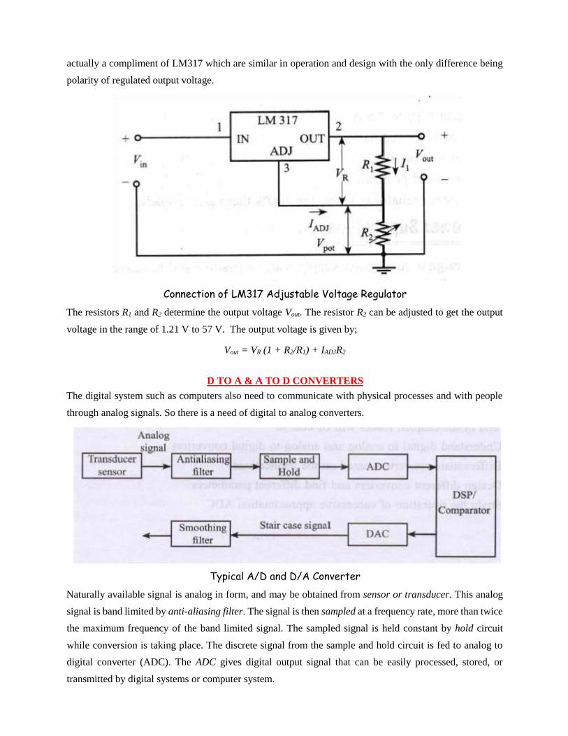
Connection of LM317 Adjustable Voltage Regulator
The resistors R1 and R2 determine the output voltage Vout. The resistor R2 can be adjusted to get the output
voltage in the range of 1.21 V to 57 V. The output voltage is given by;
Vout = VR (1 + R2/R1) + IADJR2
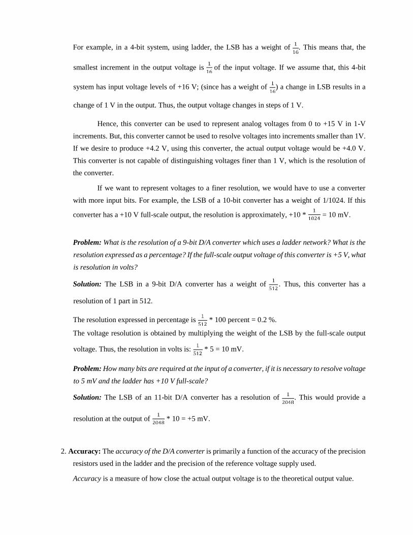
D TO A & A TO D CONVERTERS
The digital system such as computers also need to communicate with physical processes and with people
through analog signals. So there is a need of digital to analog converters.
Typical A/D and D/A Converter
Naturally available signal is analog in form, and may be obtained from sensor or transducer. This analog
signal is band limited by anti-aliasing filter. The signal is then sampled at a frequency rate, more than twice
the maximum frequency of the band limited signal. The sampled signal is held constant by hold circuit
while conversion is taking place. The discrete signal from the sample and hold circuit is fed to analog to
digital converter (ADC). The ADC gives digital output signal that can be easily processed, stored, or
transmitted by digital systems or computer system.

The digital signal is converted back to by digital to analog converter (DAC). The output of DAC is usually
stair-case waveform, which is passed through smoothing filter to reduce the quantization noise. The diagram
shown in the above Figure can be used in the applications such as digital signal processing, digital audio
mixing, music and video synthesis, data acquisition, pulse code modulation, and microprocessor
instrumentation.
BASIC DAC TECHNIQUES:
The DAC converts digital or binary data into its equivalent analog value. The symbolic representation of an
n-bit DAC is given below:
n-bit DAC
The DAC output can either be a voltage or current signal. For a voltage output DAC, the conversion
characteristic can be expressed by;
𝑉𝑉0 = 𝑘𝑘𝑉𝑉𝐹𝐹(𝑏𝑏12−1 + 𝑏𝑏22−2 + 𝑏𝑏32−3 + … 𝑏𝑏𝑖𝑖 2−𝑖𝑖)
Where, V0 – Output voltage
VFS – Full scale output voltage k – Scaling
factor (usually 1)
b1. . ., bn – n-bit binary fractional word with decimal point located at the left
b1 – MSB with a weight = VFS/2 bn – LSB with a weight = VFS/2n
Performance Parameters of DAC:
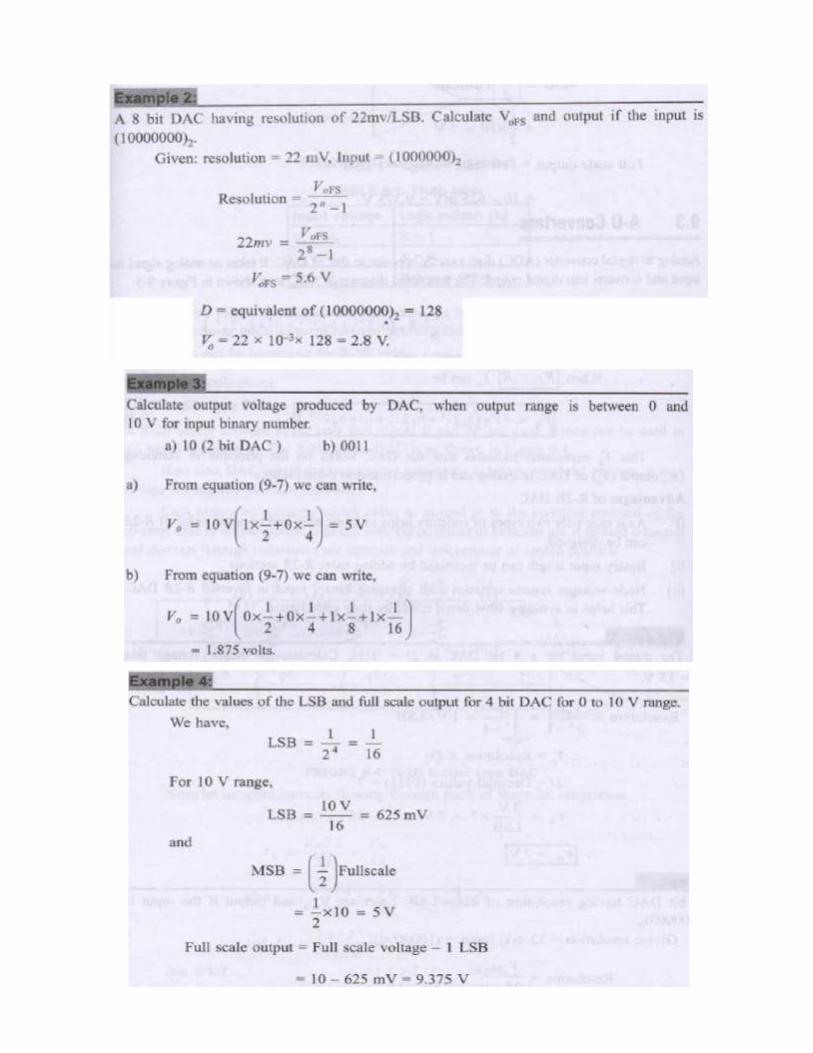
1. Resolution: Resolution is the number of various analog output values that is provided by a DAC.
For n-bit DAC; Resolution = 2n
Resolution can also be defined as the ratio of change in output voltage resulting from a change of
LSB at the digital input. For n-bit DAC; Resolution = VOFS/2n – 1
Where, VOFS – Full scale output voltage.
If we know the resolution, we can obtain input-output relation for DAC:
V0 = Resolution x b Where,
b – Decimal values of digital input.
For example, in a 4-bit system, using ladder, the LSB has a weight of . This means that, the
smallest increment in the output voltage is of the input voltage. If we assume that, this 4-bit
system has input voltage levels of +16 V; (since has a weight of ) a change in LSB results in a
change of 1 V in the output. Thus, the output voltage changes in steps of 1 V.
Hence, this converter can be used to represent analog voltages from 0 to +15 V in 1-V
increments. But, this converter cannot be used to resolve voltages into increments smaller than 1V.
If we desire to produce +4.2 V, using this converter, the actual output voltage would be +4.0 V.
This converter is not capable of distinguishing voltages finer than 1 V, which is the resolution of
the converter.
If we want to represent voltages to a finer resolution, we would have to use a converter
with more input bits. For example, the LSB of a 10-bit converter has a weight of 1/1024. If this
converter has a +10 V full-scale output, the resolution is approximately, +10 * = 10 mV.
Problem: What is the resolution of a 9-bit D/A converter which uses a ladder network? What is the
resolution expressed as a percentage? If the full-scale output voltage of this converter is +5 V, what
is resolution in volts?
Solution: The LSB in a 9-bit D/A converter has a weight of . Thus, this converter has a
resolution of 1 part in 512.
The resolution expressed in percentage is * 100 percent = 0.2 %.
The voltage resolution is obtained by multiplying the weight of the LSB by the full-scale output
voltage. Thus, the resolution in volts is: * 5 = 10 mV.
Problem: How many bits are required at the input of a converter, if it is necessary to resolve voltage
to 5 mV and the ladder has +10 V full-scale?
Solution: The LSB of an 11-bit D/A converter has a resolution of . This would provide a
resolution at the output of * 10 = +5 mV.
2. Accuracy: The accuracy of the D/A converter is primarily a function of the accuracy of the precision
resistors used in the ladder and the precision of the reference voltage supply used.
Accuracy is a measure of how close the actual output voltage is to the theoretical output value.
MAHESH PRASANNA K., VCET, PUTTUR
45
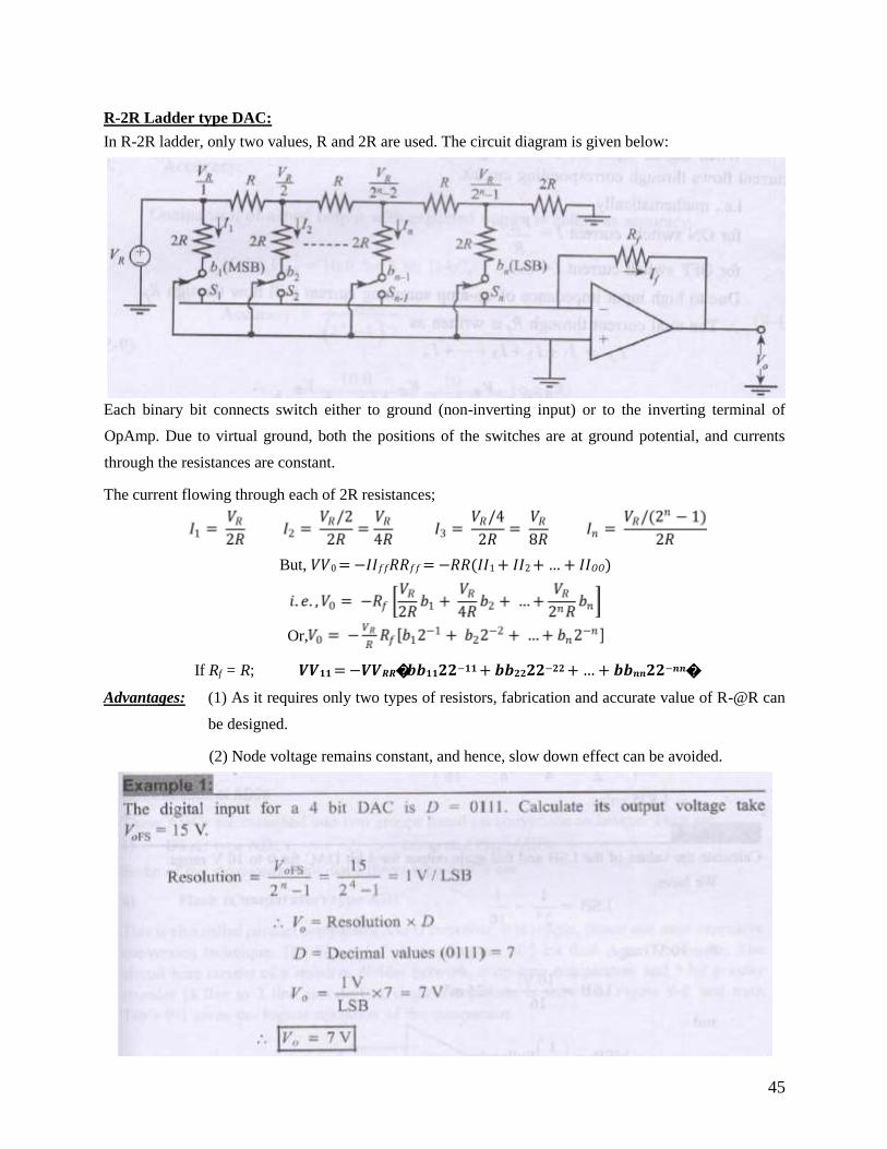
R-2R Ladder type DAC:
In R-2R ladder, only two values, R and 2R are used. The circuit diagram is given below:
Each binary bit connects switch either to ground (non-inverting input) or to the inverting terminal of
OpAmp. Due to virtual ground, both the positions of the switches are at ground potential, and currents
through the resistances are constant.
The current flowing through each of 2R resistances;
But, 𝑉𝑉0 = −𝐼𝐼𝑓𝑓𝑅𝑅𝑓𝑓 = −𝑅𝑅(𝐼𝐼1 + 𝐼𝐼2 + … + 𝐼𝐼𝑂𝑂)
Or,
If Rf = R; 𝑽𝑽𝟏𝟏 = −𝑽𝑽𝑹𝑹𝒃𝒃𝟏𝟏𝟐𝟐−𝟏𝟏 + 𝒃𝒃𝟐𝟐𝟐𝟐−𝟐𝟐 + … + 𝒃𝒃𝒏𝒏𝟐𝟐−𝒏𝒏
Advantages: (1) As it requires only two types of resistors, fabrication and accurate value of R-@R can
be designed.
(2) Node voltage remains constant, and hence, slow down effect can be avoided.

A-D CONVERTERS:
ADC takes the analog signal as input and converts into digital output. The functional diagram of DAC is
given below:
ADC is provided with two control inputs start (input to initiate the conversion) and end of conversion
(output to indicate the end of conversion). Direct type ADCs and Integrated type ADCs are the two types of
ADCs available.
Flash (Comparator/ Parallel) type ADC:
A simple, fast, but most expensive conversion technique.
A 2-bit Flash ADC:

54
A 3-bit Flash ADC:
The resistive network is to set to equal reference voltages at each node. The comparactor compares set
reference value at inverting terminal of Op-Amp with analog output at non-inverting terminal. The
truthtable for ADC is given below:

Advantages:
1. High speed Disadvantages:
1. Number of comparators required is almost double for each added bit
Eg.: For 2-bit ADC; No. of Comparators = 4 (22)
For 3-bit ADC; No. of Comparators = 8 (23)
Successive Approximation type ADC:
The following Figure shows successive approximation ADC.
MAHESH PRASANNA K., VCET, PUTTUR

Figure shows a successive approximation register (SAR), the output of which is connected to DAC and
output latch circuit. The input signal (Vin) is compared with the analog output signal (Va) of the DAC. Output
of the comparator is feedback into SAR. The control logic inside SAR adjusts its digital output; until it is
equal to the analog input signal. The operation could be understood by the code tree given below.
At the start of conversion cycle, start conversion terminal is made high. On the first clock pulse, the output
of the SAR is made 1000. The DAC produces an analog voltage (Va) proportional to 1000. This analog
voltage is compared with input analog signal (Vin).
If Vin > Va, the comparator output will be high and SAR keeps Q3 high. On the other hand, if Vin < Va, then
the comparator output becomes low and SAR resets Q3 to low. If Vin > Va, SAR follows the upward path
in code tree and if Vin < Va, SAR follows downward path.
The conversion time for n-bit successive approximation ADC is (n + 2) clock periods.
Advantages:
1. Considerably good speed
2. Good resolution.

References
Books:
1. Charles H Roth and Larry L Kinney, Analog and Digital Electronics, Cengage Learning, 2019
2. Anil K Maini, Varsha Agarwal, Electronic Devices and Circuits, Wiley, 2012.
Website Links:
https://circuitglobe.com/photodiode.html
https://www.tutorialspoint.com/linear_integrated_circuits_applications/index.htm
https://www.elprocus.com/digital-to-analog-converter-dac-applications/
https://www.electronicshub.org/photodiode-working-characteristics-applications/
https://www.electrical4u.com/applications-of-op-amp/
Question Bank:
Explain the working of construction and working of Astable multivibrator using 555 timer IC
Explain the working of Photodiode with necessary circuit diagram.
Explain the construction and working of Relaxation oscillator.
Explain the working of R2R DAC with necessary circuit diagram & derivations.
.
Explain the construction, working principles and characteristics of photodiodes.
Explain the construction, working principles and applications of light emitting diode (LED).
Explain peak detector circuit with a neat waveform.
With a neat diagram explain R-2R ladder network DAC.
Explain the operation of successive approximation ADC using simplified block diagram.
Explain peak detector circuit with a neat waveform.
Explain Astable multivibrator with neat circuit diagram and waveform.
University Questions:

1
18CS33
PREREQUISITES:
ANALOG AND DIGITAL ELECTRONICS
MODULE – 2
THE COMBINATIONAL LOGIC CIRCUITS
THE BASIC GATES
Electronic circuits and systems can be divided into two broad categories – analog and digital. Analog
circuits are designed for use with small signals and are used in a linear fashion. Digital circuits are generally
used with large signals and are considered nonlinear. Any quantity that changes with time can be
represented as an analog signal or it can be treated as digital signal.
Digital electronics involves circuits that have exactly two possible states. A system having only
two states is said to be binary. The binary number system is widely used in digital electronics.
Hexa-Decimal Decimal Binary Hexa-Decimal Decimal Binary
0 0 0 0 0 0 8 8 1 0 0 0
1 1 0 0 0 1 9 9 1 0 0 1
2 2 0 0 1 0 A 10 1 0 1 0
3 3 0 0 1 1 B 11 1 0 1 1
4 4 0 1 0 0 C 12 1 1 0 0
5 5 0 1 0 1 D 13 1 1 0 1
6 6 0 1 1 0 E 14 1 1 1 0
7 7 0 1 1 1 F 15 1 1 1 1
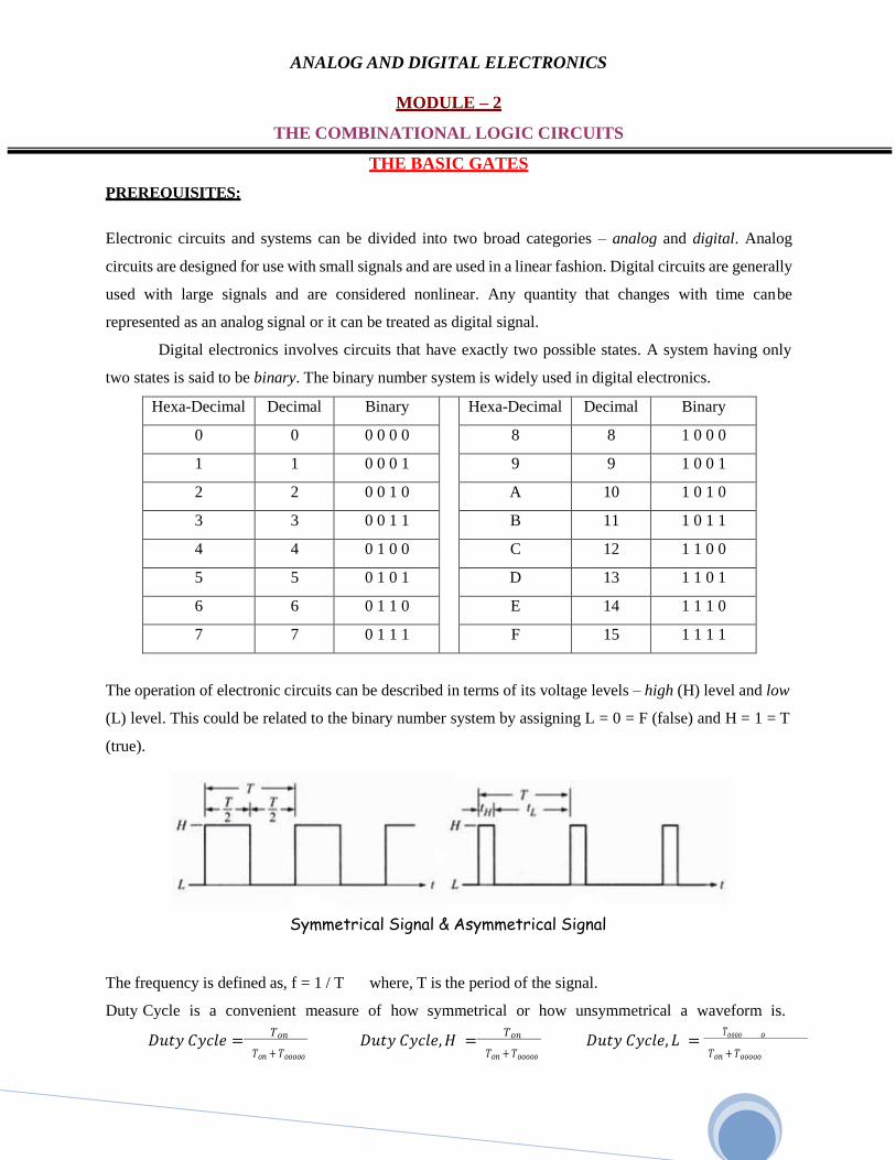
The operation of electronic circuits can be described in terms of its voltage levels – high (H) level and low
(L) level. This could be related to the binary number system by assigning L = 0 = F (false) and H = 1 = T
(true).
Symmetrical Signal & Asymmetrical Signal
The frequency is defined as, f = 1 / T where, T is the period of the signal.
Duty Cycle is a convenient measure of how symmetrical or how unsymmetrical a waveform is.
𝐷𝑢𝑡𝑦 𝐶𝑦𝑐𝑙𝑒 = 𝑇𝑜𝑛
𝑇𝑜𝑛 + 𝑇𝑜𝑜𝑜𝑜𝑜
𝐷𝑢𝑡𝑦 𝐶𝑦𝑐𝑙𝑒, 𝐻 = 𝑇𝑜𝑛
𝑇𝑜𝑛 + 𝑇𝑜𝑜𝑜𝑜𝑜
𝐷𝑢𝑡𝑦 𝐶𝑦𝑐𝑙𝑒, 𝐿 = 𝑇𝑜𝑜𝑜𝑜 𝑜
𝑇𝑜𝑛 + 𝑇𝑜𝑜𝑜𝑜𝑜
2
18CS33
ANALOG AND DIGITAL ELECTRONICS
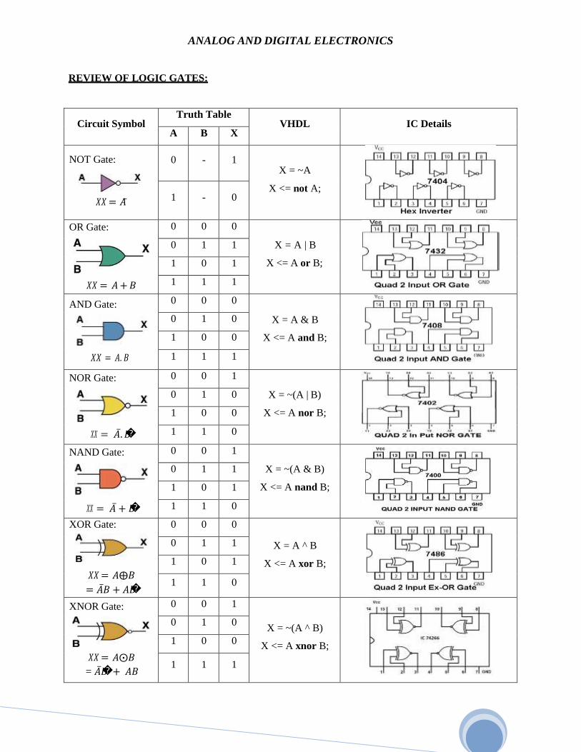
REVIEW OF LOGIC GATES:
Circuit Symbol Truth Table
VHDL IC Details A B X
NOT Gate:
𝑋𝑋 = 𝐴
0 - 1 X = ~A
X <= not A;
1 - 0
OR Gate:
𝑋𝑋 = 𝐴 + 𝐵
0 0 0 X = A | B
X <= A or B;
0 1 1
1 0 1
1 1 1
AND Gate:
𝑋𝑋 = 𝐴. 𝐵
0 0 0 X = A & B
X <= A and B;
0 1 0
1 0 0
1 1 1
NOR Gate:
𝑋𝑋 = 𝐴 . 𝐵
0 0 1 X = ~(A | B)
X <= A nor B;
0 1 0
1 0 0
1 1 0
NAND Gate:
𝑋𝑋 = 𝐴 + 𝐵
0 0 1 X = ~(A & B)
X <= A nand B;
0 1 1
1 0 1
1 1 0
XOR Gate:
𝑋𝑋 = 𝐴⨁𝐵
= 𝐴 𝐵 + 𝐴𝐵
0 0 0
X = A ^ B
X <= A xor B;
0 1 1
1 0 1
1 1 0
XNOR Gate:
𝑋𝑋 = 𝐴⨀𝐵
= 𝐴 𝐵 + 𝐴𝐵
0 0 1
X = ~(A ^ B)
X <= A xnor B;
0 1 0
1 0 0
1 1 1

3
Universality of NOR Gate:
ANALOG AND DIGITAL ELECTRONICS
Universality of NAND Gate:
Bubbled AND Gate:
Bubbled AND gate and NOR gate are equivalent
De Morgan’s First Theorem:
The complement of a sum equals the product of the complements. 𝐴 + 𝐵 = 𝐴 . 𝐵
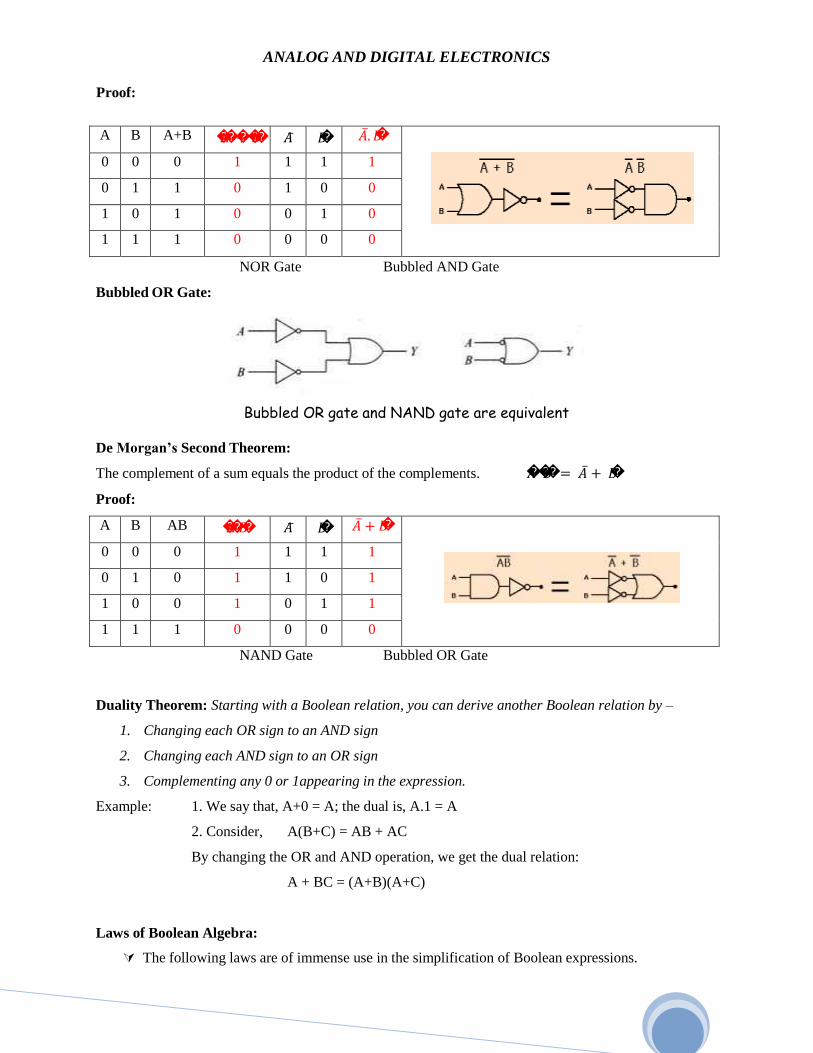
4
18CS33
Proof:
ANALOG AND DIGITAL ELECTRONICS
A B A+B 𝐴 + 𝐵 𝐴 𝐵 𝐴 . 𝐵
0 0 0 1 1 1 1
0 1 1 0 1 0 0
1 0 1 0 0 1 0
1 1 1 0 0 0 0
Bubbled OR Gate:
NOR Gate Bubbled AND Gate
Bubbled OR gate and NAND gate are equivalent
De Morgan’s Second Theorem:
The complement of a sum equals the product of the complements. 𝐴 𝐵 = 𝐴 + 𝐵
Proof:
A B AB 𝐴𝐵 𝐴 𝐵 𝐴 + 𝐵
0 0 0 1 1 1 1
0 1 0 1 1 0 1
1 0 0 1 0 1 1
1 1 1 0 0 0 0
NAND Gate Bubbled OR Gate
Duality Theorem: Starting with a Boolean relation, you can derive another Boolean relation by –
1. Changing each OR sign to an AND sign
2. Changing each AND sign to an OR sign
3. Complementing any 0 or 1appearing in the expression.
Example: 1. We say that, A+0 = A; the dual is, A.1 = A
2. Consider, A(B+C) = AB + AC
By changing the OR and AND operation, we get the dual relation:
A + BC = (A+B)(A+C)
Laws of Boolean Algebra:
The following laws are of immense use in the simplification of Boolean expressions.

5
18CS33
ANALOG AND DIGITAL ELECTRONICS
Note that, if A is a variable, then either A = 0 or A = 1. Also, when A = 0, A ≠ 1;
and when A = 1, A ≠ 0.
De Morgan’s First Theorem:-
The complement of sum is equal to the product of the complements.
(A + B)’ = A’ . B’ i.e., a bubbled AND gate & a NOR gate are equivalent.
De Morgan’s Second Theorem:-
The complement of a product is equal to the sum of the compliments.
(A . B)’ = A’ + B’ i.e., a bubbled OR gate & a NAND gate are equivalent.
1) Commutative Law:-
A + B = B + A and A . B = B . A
2) Associative Law:-
A + (B + C) = (A + B) + C and A . (BC) = (AB) . C
3) Distributive Law:-
A(B + C) = AB + AC
4) In relation to OR operation, the following laws hold good:-
A + 0 = A
A + A = A
A + 1 = 1 and
A + A’ = 1
5) In relation to AND operation, the following laws hold good:-
A . 1 = A
A . A = A
A . 0 = 0
A . A’ = 0
A’’ = A
6) Some more useful Boolean relations:-
A + AB = A
A + A’B = A + B
A (A + B) = A
A (A’ + B) = AB
A + (B . C) = (A + B) (A + C)
6
18CS33
ANALOG AND DIGITAL ELECTRONICS
Simplification of Boolean Expressions:-
The following hints are found to be of use, in reducing complex Boolean expressions –
1. If there are parentheses present in the given expression, they are removed first; since,
multiplication should precede addition.
E.g.:- AB + C (A + B) = AB + AC + BC
2. If there are several identical terms, all except one can be removed.
E.g.:- A + B + C + A . 1 = A + B + C + A = A + B + C
3. If a variable repeats in a term, only one variable may be retained.
E.g.:- A . A = A
B .B . C = BC
4. If in any term, both a variable & its complement are present, that term may be removed; since,
AA’ = 0.
E.g.:- XX’Y = 0 . Y = 0
5. Identify pairs of terms which contains same variables. If in a pair, a variable is absent in one term,
it can be removed.
E.g.:- ABCD + ABC = ABC (D + 1)
= ABC . 1 since, 1 + D =1
= ABC
6. If, in a pair of terms, several variables are common, and another variable is present in one term &
its complement is present in another term, this variable & its complement can be removed.
E.g.:- ABC + A’BC = BC (A’ + A)
= BC . 1 since, A’ + A = 1
= BC
KARNAUGH MAPS
MINIMUM FORMS OF SWITCHING FUNCTIONS:
When a function is realized using AND and OR gates, the cost of realizing the function is directly related
to the number of gates and gate inputs used. The Karnaugh map techniques developed, lead directly to
minimum cost two-level circuits composed of AND and OR gates. An expression consisting of a sum-of-
product terms corresponds directly to a two-level circuit composed of a group of AND gates feeding a
single OR gate (see the following Figure). Similarly, a product-of-sums expression corresponds to a two-
level circuit composed of OR gates feeding a single AND gate.
Therefore, to find minimum cost two-level AND-OR gate circuits, we must find minimum expressions in
sum-of-products or product-of-sums form.

7
18CS33
ANALOG AND DIGITAL ELECTRONICS
A minimum sum-of-products expression for a function is defined as a sum of product terms which
a) has a minimum number of terms and
b) of all those expressions which have the same minimum number of terms, has a minimum number
of literals.
The minimum sum of products corresponds directly to a minimum two-level gate circuit which has
a) a minimum number of gates and
b) a minimum number of gate inputs.
Unlike the minterm expansion for a function, the minimum sum of products is not necessarily unique; that
is, a given function may have two different minimum sum-of-products forms, each with the same number
of terms and the same number of literals.
Given a minterm expansion, the minimum sum-of products form can often be obtained by the following
procedure:
1. Combine terms by using 𝑋𝑋𝑌′ + 𝑋𝑋𝑌 = 𝑋𝑋(𝑌′ + 𝑌) = 𝑋𝑋. Do this repeatedly to eliminate as many
literals as possible. A given term may be used more than once because X+X=X.
2. Eliminate redundant terms by using the theorems of Boolean Algebra.
A minimum product-of-sums expression for a function is defined as a product of sum terms which
a) has a minimum number of factors, and
b) of all those expressions which have the same number of factors, has a minimum number of literals.
Unlike the maxterm expansion, the minimum product-of-sums form of a function is not necessarily unique.
Given a maxterm expansion, the minimum product of sums can often be obtained by a procedure similar to
that used in the minimum sum-of-products case, except that the theorem (𝑋𝑋 + 𝑌′ )(𝑋𝑋 + 𝑌) = 𝑋𝑋 is used to
combine terms.
8
18CS33
ANALOG AND DIGITAL ELECTRONICS
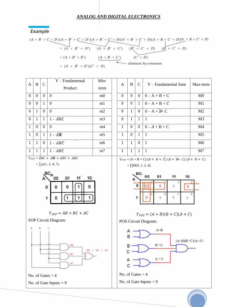
A B C Y – Fundamental
Product
Min-
term
A B C Y – Fundamental Sum Max-term
0 0 0 0 m0 0 0 0 0 – A + B + C M0
0 0 1 0 m1 0 0 1 0 – A + B + 𝐶 M1
0 1 0 0 m2 0 1 0 0 – A + 𝐵 + C M2
0 1 1 1 – 𝐴 𝐵𝐶 m3 0 1 1 1 M3
1 0 0 0 m4 1 0 0 0 – 𝐴 + B + C M4
1 0 1 1 – 𝐴𝐵 𝐶 m5 1 0 1 1 M5
1 1 0 1 – 𝐴𝐵𝐶 m6 1 1 0 1 M6
1 1 1 1 – 𝐴𝐵𝐶 m7 1 1 1 1 M7
YSOP = 𝐴 𝐵𝐶 + 𝐴𝐵 𝐶 + 𝐴𝐵𝐶 + 𝐴𝐵𝐶
= ∑m(1, 2, 4, 7).
𝑌𝑆𝑂𝑃 = 𝐴𝐵 + 𝐵𝐶 + 𝐴𝐶
SOP Circuit Diagram:
No. of Gates = 4
No. of Gate Inputs = 9
YPOS = (A + B + C) (𝐴 + 𝐵 + 𝐶 ) (𝐴 + 𝐵 + 𝐶) (𝐴 + 𝐵 + 𝐶)
= ∏M(0, 1, 2, 4).
𝑌𝑃𝑂𝑆 = (𝐴 + 𝐵)(𝐵 + 𝐶)(𝐴 + 𝐶)
POS Circuit Diagram:
No. of Gates = 4
No. of Gate Inputs = 9
9
18CS33
ANALOG AND DIGITAL ELECTRONICS
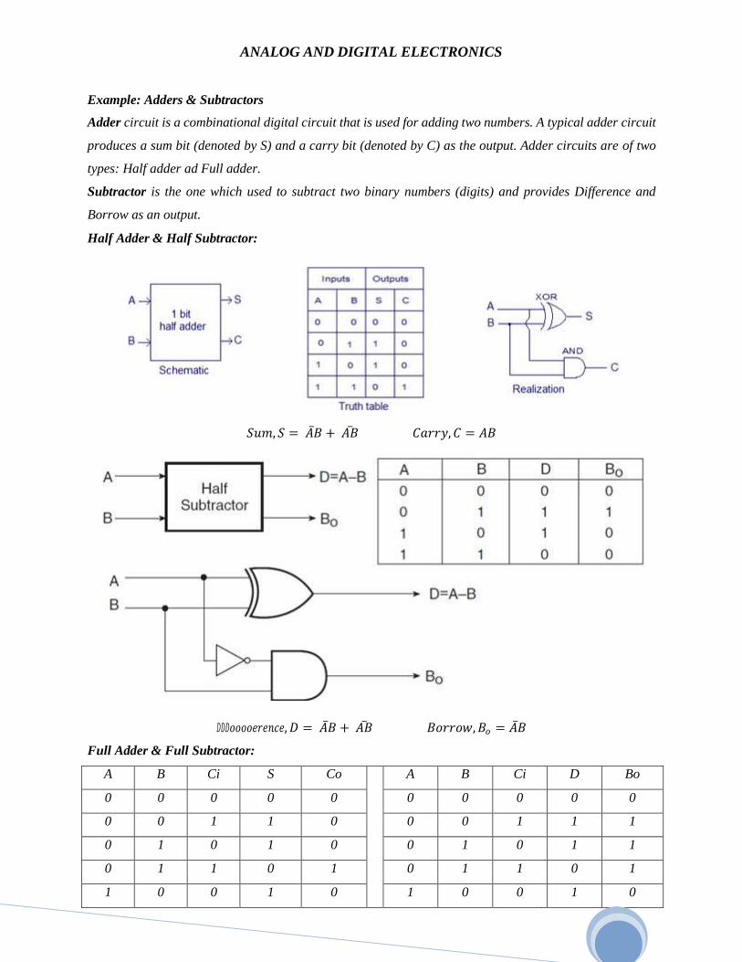
Example: Adders & Subtractors
Adder circuit is a combinational digital circuit that is used for adding two numbers. A typical adder circuit
produces a sum bit (denoted by S) and a carry bit (denoted by C) as the output. Adder circuits are of two
types: Half adder ad Full adder.
Subtractor is the one which used to subtract two binary numbers (digits) and provides Difference and
Borrow as an output.
Half Adder & Half Subtractor:
𝑆𝑢𝑚, 𝑆 = 𝐴 𝐵 + 𝐴𝐵 𝐶𝑎𝑟𝑟𝑦, 𝐶 = 𝐴𝐵
𝐷𝐷𝐷𝑜𝑜𝑜𝑜𝑒𝑟𝑒𝑛𝑐𝑒, 𝐷 = 𝐴 𝐵 + 𝐴𝐵 𝐵𝑜𝑟𝑟𝑜𝑤, 𝐵𝑜 = 𝐴 𝐵
Full Adder & Full Subtractor:
A B Ci S Co A B Ci D Bo
0 0 0 0 0 0 0 0 0 0
0 0 1 1 0 0 0 1 1 1
0 1 0 1 0 0 1 0 1 1
0 1 1 0 1 0 1 1 0 1
1 0 0 1 0 1 0 0 1 0

10
18CS33
ANALOG AND DIGITAL ELECTRONICS
1 0 1 0 1 1 0 1 0 0
1 1 0 0 1 1 1 0 0 0
1 1 1 1 1 1 1 1 1 1
Sum, S = ∑m (1, 2, 4, 7) = ∏M(0, 3 , 5, 6). Difference, D = ∑m (1, 2, 4, 7) = ∏M(0, 3, 5, 6).
𝑆𝑢𝑚, 𝑆 = 𝐴 𝐵 𝐶 + 𝐴 𝐵𝐶 + 𝐴𝐵 𝐶 + 𝐴𝐵𝐶 𝐷𝐷𝐷𝑜𝑜𝑜𝑜. , 𝐷 = 𝐴 𝐵 𝐶 + 𝐴 𝐵𝐶 + 𝐴𝐵 𝐶 + 𝐴𝐵𝐶
𝑂𝑟, 𝑆 = 𝐶 (𝐴 𝐵 + 𝐴𝐵 ) + 𝐶(𝐴 𝐵 + 𝐴𝐵) 𝑂𝑟, 𝐷 = 𝐶 (𝐴 𝐵 + 𝐴𝐵 ) + 𝐶(𝐴 𝐵 + 𝐴𝐵)
𝑂𝑟, 𝑆 = 𝐶 (𝐴⨁𝐵) + 𝐶(𝐴 ⊙ 𝐵) 𝑂𝑟, 𝐷 = 𝐶 (𝐴⨁𝐵) + 𝐶(𝐴 ⊙ 𝐵)
𝑂𝑟, 𝑆 = 𝐶 (𝐴⨁𝐵) + 𝐶(𝐴 ⊕ 𝐵 ) 𝑂𝑟, 𝐷 = 𝐶 (𝐴⨁𝐵) + 𝐶(𝐴 ⊕ 𝐵 )
𝑇ℎ𝑒𝑟𝑒𝑜𝑜𝑜𝑟𝑒, 𝑆 = 𝐴 ⊕ 𝐵 ⊕ 𝐶 𝑇ℎ𝑒𝑟𝑒𝑜𝑜𝑜𝑟𝑒, 𝐷 = 𝐴 ⊕ 𝐵 ⊕ 𝐶
Carry Out, Co = ∑m (3, 5, 6, 7) = ∏M(0, 1, 2, 4). Borrow, Bo = ∑m (1, 2, 3, 7) = ∏M(0, 4, 5, 6).
𝐶𝑎𝑟𝑟𝑦 𝑂𝑢𝑡, 𝐶𝑜 = 𝐴 𝐵𝐶 + 𝐴𝐵 𝐶 + 𝐴𝐵𝐶 + 𝐴𝐵𝐶 𝐵𝑜𝑟𝑟𝑜𝑤, 𝐵𝑜 = 𝐴 𝐵 𝐶 + 𝐴 𝐵𝐶 + 𝐴 𝐵𝐶 + 𝐴𝐵𝐶
𝑂𝑟, 𝐶𝑜 = 𝐶 (𝐴𝐵) + 𝐶(𝐴 𝐵 + 𝐴𝐵 + 𝐴𝐵) 𝑂𝑟, 𝐵𝑜 = 𝐶 (𝐴 𝐵) + 𝐶(𝐴 𝐵 + 𝐴 𝐵 + 𝐴𝐵)
𝑇ℎ𝑒𝑟𝑒𝑜𝑜𝑜𝑟𝑒, 𝐶𝑜 = 𝐴𝐵 + 𝐵𝐶 + 𝐴𝐶 𝑇ℎ𝑒𝑟𝑒𝑜𝑜𝑜𝑟𝑒, 𝐵𝑜 = 𝐴𝐵 + 𝐵𝐶 + 𝐴𝐶
11
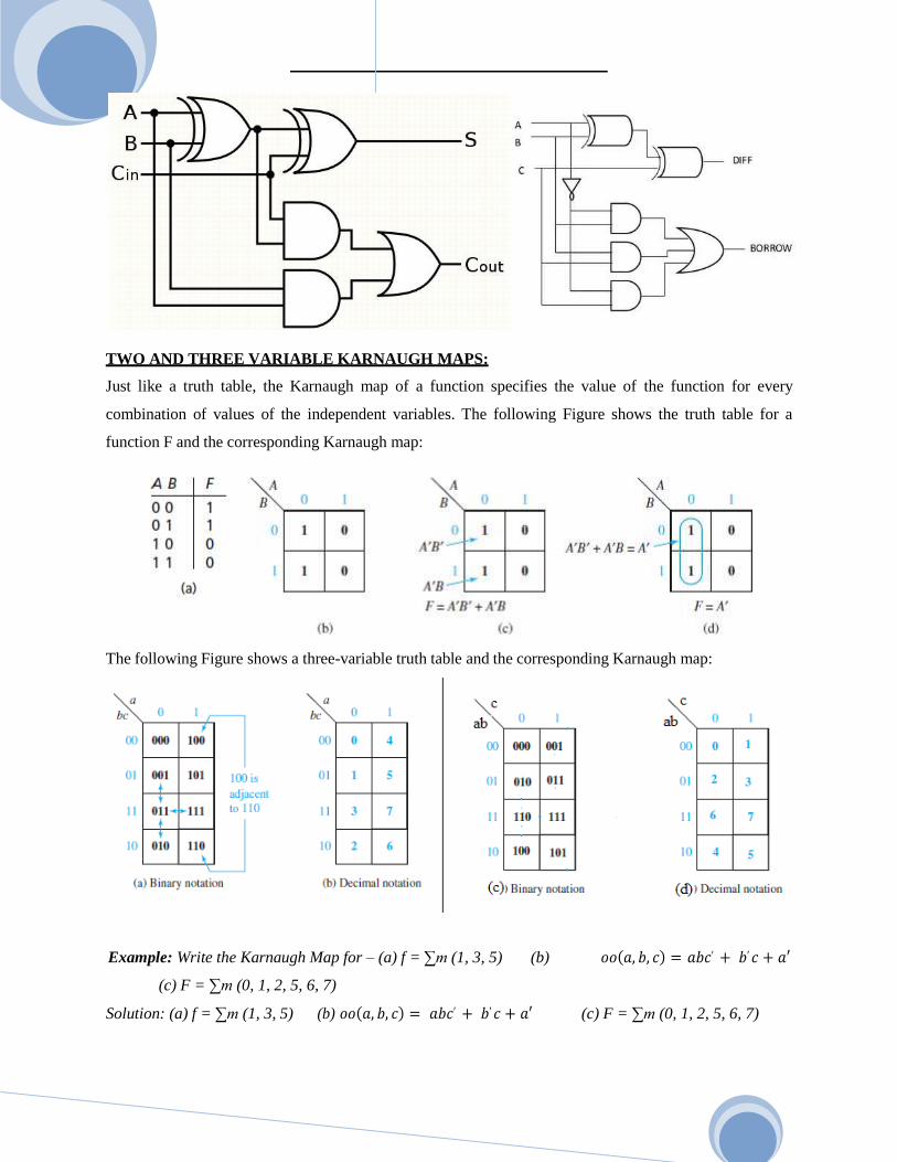
TWO AND THREE VARIABLE KARNAUGH MAPS:
Just like a truth table, the Karnaugh map of a function specifies the value of the function for every
combination of values of the independent variables. The following Figure shows the truth table for a
function F and the corresponding Karnaugh map:
The following Figure shows a three-variable truth table and the corresponding Karnaugh map:
Example: Write the Karnaugh Map for – (a) f = ∑m (1, 3, 5) (b) 𝑜𝑜(𝑎, 𝑏, 𝑐) = 𝑎𝑏𝑐′ + 𝑏′ 𝑐 + 𝑎′
(c) F = ∑m (0, 1, 2, 5, 6, 7)
Solution: (a) f = ∑m (1, 3, 5) (b) 𝑜𝑜(𝑎, 𝑏, 𝑐) = 𝑎𝑏𝑐′ + 𝑏′ 𝑐 + 𝑎′ (c) F = ∑m (0, 1, 2, 5, 6, 7)
12
f 𝑎 𝑏 𝑎 𝑏 ab 𝑎𝑏
𝑐𝑑
𝑐d
𝑐𝑑
𝑐𝑑
f 00 01 11 10
00
01
11
10
ANALOG AND DIGITAL ELECTRONICS
Example: Find two different minimum sum-of-products expressions for the function G = ∑m (0, 2, 3, 4, 5,
7).
Solution: Given, G = ∑m (0, 2, 3, 4, 5, 7);
FOUR-VARIABLE KARNAUGH MAPS:
The following Figure shows the location of minterms on a four-variable map & plot of four-variable
expression 𝑜𝑜(𝑎, 𝑏, 𝑐, 𝑑) = 𝑎𝑐𝑑 + 𝑎′ 𝑏 + 𝑑′ on a Karnaugh map:
f (a, b, c, d) =
Example: Write the Karnaugh map for (a) 𝑜𝑜 = 𝑥′ 𝑧′ + 𝑤𝑥𝑦 + 𝑥′ 𝑦
(b) 𝑌 = 𝐴 𝐵 𝐶 + 𝐴 𝐵𝐶 + 𝐴𝐵 𝐶 + 𝐴𝐵𝐶
0 4 12 8
1 5 13 9
3 7 15 11
2 6 14 10

13
3
Solution:
ANALOG AND DIGITAL ELECTRONICS
f
𝑦 𝑧
𝑦 𝑧
𝑦𝑧
𝑦𝑧
𝑤 𝑥 𝑤 𝑥 wx 𝑤𝑥 Y 0 1
00
01
11
10
f (w, x, y, z) = Y (A, B, C) =
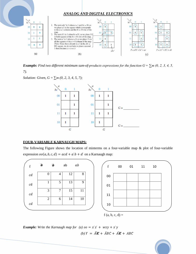
Example: Write the Karnaugh map for (a) f1 = = ∑m (3, 4, 5, 6, 7, 9, 12, 13); (b) f2 = = ∑m (2, 3, 5, 7,
8, 10, 11, 15).
Solution: (a) Given, f1 = = ∑m (3, 4, 5, 6, 7, 9, 12, 13) & f2 = = ∑m (2, 3, 5, 7, 8, 10, 11, 15);
DETERMINATION OF MINIMUM EXPRESSIONS USING ESSENTIAL PRIME
IMPLICANTS:
Any single 1 or any group of 1’s which can be combined together on a map of the function F represents a
product term which is called an implicant of F. Several implicants of F MAY BE POSSIBLE. A product
term implicant is called a prime implicant if it cannot be combined with another term to eliminate a variable.
The following Figure shows the flowchart for determining a Minimum Sum of Products using a Karnaugh
Map with an Example.
14
ANALOG AND DIGITAL ELECTRONICS
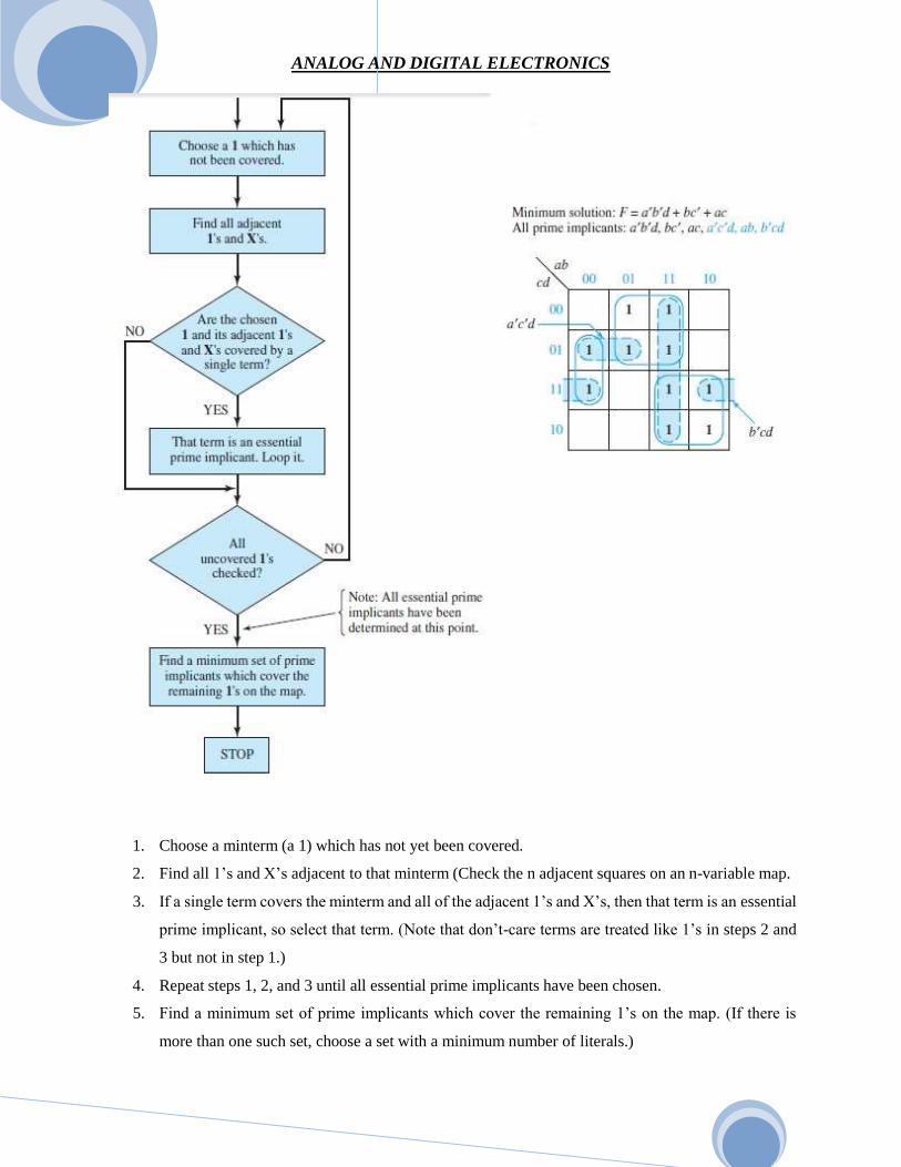
1. Choose a minterm (a 1) which has not yet been covered.
2. Find all 1’s and X’s adjacent to that minterm (Check the n adjacent squares on an n-variable map.
3. If a single term covers the minterm and all of the adjacent 1’s and X’s, then that term is an essential
prime implicant, so select that term. (Note that don’t-care terms are treated like 1’s in steps 2 and
3 but not in step 1.)
4. Repeat steps 1, 2, and 3 until all essential prime implicants have been chosen.
5. Find a minimum set of prime implicants which cover the remaining 1’s on the map. (If there is
more than one such set, choose a set with a minimum number of literals.)

15
Y 𝐴 𝐵 𝐴 𝐵 AB A𝐵
𝐶 𝐷
𝐶 D
𝐶𝐷
𝐶𝐷
Y 𝐴 𝐵 𝐴 𝐵 AB A𝐵
𝐶 𝐷
𝐶 D
𝐶𝐷
𝐶𝐷
ANALOG AND DIGITAL ELECTRONICS
PAIRS, QUADS, AND OCTETS:
Pairs: The following K-map contains a pair of 1s that are horizontally adjacent. Two adjacent 1s, such as
these are called a pair. A pair eliminates one variable and its complement.
The sum-of-product equation is:
𝑌 = 𝐴𝐵𝐶𝐷 + 𝐴𝐵𝐶𝐷′ = 𝐴𝐵𝐶(𝐷 + 𝐷′ ) = 𝐴𝐵𝐶
Quad: A quad is a group of four 1s that are horizontally or vertically adjacent. A quad eliminates two
variables and their complements.
The sum-of-product equation is:
𝑌 = 𝐴𝐵𝐶′ + 𝐴𝐵𝐶 = 𝐴𝐵(𝐶 + 𝐶′ ) = 𝐴𝐵
The Octet: The octet is a group of eight 1s, as shown in the following Fig. An octet eliminates three
variables and their complements.
The sum-of-product equation is:
𝑌 = 𝐴𝐵 + 𝐴𝐵′ = 𝐴(𝐵 + 𝐵′) = 𝐴
Y 𝐴 𝐵 𝐴 𝐵 AB A𝐵
𝐶 𝐷
𝐶 D
𝐶𝐷
𝐶𝐷
0 0 0 0
0 0 0 0
0 0 1 0
0 0 1 0
0 0 1 0
0 0 1 0
0 0 1 0
0 0 1 0
0 0 1 1
0 0 1 1
0 0 1 1
0 0 1 1

16
Y1 𝐴 𝐵 𝐴 𝐵 AB A𝐵
𝐶 𝐷
𝐶 D
𝐶𝐷
𝐶𝐷
Y2 𝐴 𝐵 𝐴 𝐵 AB A𝐵
𝐶 𝐷
𝐶 D
𝐶𝐷
𝐶𝐷
Y3 𝐴 𝐵 𝐴 𝐵 AB A𝐵
𝐶 𝐷
𝐶 D
𝐶𝐷
𝐶𝐷
Y4 𝐴 𝐵 𝐴 𝐵 AB A𝐵
𝐶 𝐷
𝐶 D
𝐶𝐷
𝐶𝐷
ANALOG AND DIGITAL ELECTRONICS
KARNAUGH SIMPLIFICATIONS:
A pair eliminates one variable and its complement. A quad eliminates two variables and their complements.
An octet eliminates three variables and their complements. Because of this, after drawing the K-map, first
encircle the octets, then the quads, and finally the pairs, to get highest simplification.
Example: Using K-map, simplify; Y = ∑m (1, 2, 3, 6, 8, 9, 10, 12, 13, 14).
𝑌 = 𝐴𝐶′ + 𝐶𝐷′ + 𝐴′𝐵′𝐷
Overlapping Groups: Always overlap groups.
Y1 = Y2 =
Rolling the Map:
Y3 = Y4 =
Solution:
Y 𝐴 𝐵 𝐴 𝐵 AB A𝐵
𝐶 𝐷
𝐶 D
𝐶𝐷
𝐶𝐷
0 0 1 1
1 0 1 1
1 0 0 0
1 1 1 1
0 0 0 0
0 1 0 0
1 1 1 1
1 1 1 1
0 0 0 0
0 1 0 0
1 1 1 1
1 1 1 1
0 0 0 0
1 0 0 1
1 0 0 1
0 0 0 0
0 0 0 0
1 0 0 1
1 0 0 1
0 0 0 0

17
𝐶 𝐷
𝐶 D
𝐶𝐷
𝐶𝐷
Rolling and Overlapping:
ANALOG AND DIGITAL ELECTRONICS
Y1
𝐶 𝐷
𝐶 D
𝐶𝐷
𝐶𝐷
𝐴 𝐵 𝐴 𝐵 AB A𝐵
1 1 0 0
1 1 0 1
1 1 0 1
1 1 0 0
Y2 𝐴 𝐵 𝐴 𝐵 AB A𝐵
1 1 0 0
1 1 0 1
1 1 0 1
1 1 0 0
Y1 = Y2 =
𝐶 𝐷
𝐶 D
𝐶𝐷
𝐶𝐷
𝐴 𝐵 𝐴 𝐵 AB A𝐵
1 1 0 1
1 1 0 1
1 1 0 0
1 1 0 1
Y4
𝐶 𝐷
𝐶 D
𝐶𝐷
𝐶𝐷
𝐴 𝐵 𝐴 𝐵 AB Y5
𝐶 𝐷
𝐶 D
𝐶𝐷
𝐶𝐷
𝐴 𝐵 𝐴 𝐵 AB A𝐵
Y3 = Y4 = Y5 =
Eliminating Redundant Groups: After encircling groups, eliminate any redundant groups. This is a
group whose 1s are already used by other groups.
𝐶 𝐷
𝐶 D
𝐶𝐷
𝐶𝐷
𝐴 𝐵 𝐴 𝐵 AB A𝐵
0 0 1 0
1 1 1 0
0 1 1 1
0 1 0 0
Y
𝐶 𝐷
𝐶 D
𝐶𝐷
𝐶𝐷
𝐴 𝐵 𝐴 𝐵 AB A𝐵
Y
𝐶 𝐷
𝐶 D
𝐶𝐷
𝐶𝐷
𝐴 𝐵 𝐴 𝐵 AB A𝐵
A𝐵
1 1 0 1
1 1 0 1
1 1 0 0
1 1 0 1
1 1 0 1
1 1 0 1
1 1 0 0
1 1 0 1
0 0 1 0
1 1 1 0
0 1 1 1
0 1 0 0
0 0 1 0
1 1 1 0
0 1 1 1
0 1 0 0
18
Homework:
ANALOG AND DIGITAL ELECTRONICS
1] Determine the minimum sum-of-products for –
a) f1 (a, b, c) = ∑(1, 3, 4, 5, 6, 7)
b) f2 (a, b, c) = Π (2, 4, 7)
c) f3 (a, b, c, d) = 𝑏′ 𝑐′ 𝑑′ + 𝑏𝑐𝑑 + 𝑎𝑐𝑑′ + 𝑎′ 𝑏′ 𝑐 + 𝑎′𝑏𝑐′𝑑
2] Determine the minimum product-of-sums for –
a) f1 (a, b, c) = ∑ (0, 1, 2,3, 4, 6, 7)
b) f2 (a, b, c) = Π (1, 4, 5)
c) f3 (a, b, c, d) = 𝑏′ 𝑐′ 𝑑′ + 𝑏𝑐𝑑 + 𝑎𝑐𝑑′ + 𝑎′ 𝑏′ 𝑐 + 𝑎′𝑏𝑐′𝑑
3] Solve for the simplified Boolean expression using K-Map:
a) 𝑜𝑜1 (𝑎, 𝑏, 𝑐, 𝑑) = 𝑎 𝑐𝑑 + 𝑎 𝑐𝑑 + 𝑏 𝑐 𝑑 + 𝑎𝑏 𝑐 + 𝑎 𝑏 𝑐𝑑
b) 𝑜𝑜2 (𝑎, 𝑏, 𝑐, 𝑑) = 𝑎 + 𝑏 + 𝑑 𝑎 + 𝑏 + 𝑑 𝑎 + 𝑏 + 𝑐 + 𝑑𝑎 + 𝑏 + 𝑐 + 𝑑 (𝑎 + 𝑏 + 𝑐 +
𝑑)
4] Find the minimum sum-of-products for –
(a) f1 (a, b, c) = m0 + m2 + m5 + m6 (b) f2 (d, e, f) = ∑m (0, 1, 2, 4)
(c) f3 (r, s, t) = 𝑟𝑡′ + 𝑟′ 𝑠′ + 𝑟′𝑠) (d) f4 (x, y, z) = M0 . M5
5] Design a 3-input, 1-output, minimal two-level gate combinational circuit; which has an output equal to
1 when majority of its inputs are at logic 1, and has output 0 when majority of inputs are at logic 0.
6] Design a minimal sum and minimal product combinational gate circuit to generate the odd parity bit
for an 8421 BCD code.
QUINE McCLUSKEY (QM) METHOD
The Karnaugh map method is an effective way to simplify switching functions which have a small number
of variables. When the number of variables is large or if several functions must be simplified, the use of a
digital computer is desirable.
The Quine-McCluskey method provides a systematic simplification procedure which can be readily
programmed for a digital computer. The Quine-McCluskey method reduces the minterm expansion
(standard sum-of-products form) of a function to obtain a minimum sum of products.
DETERMINATION OF PRIME IMPLICANTS:
In order to apply the Quine-McCluskey method to determine a minimum sum-of-products
expression for a function, the function must be given as a sum of minterms.
In the first part of the Quine-McCluskey method, all of the prime implicants of a function are
systematically formed by combining minterms.

19
ANALOG AND DIGITAL ELECTRONICS
Two minterms will combine if they differ in exactly one variable. The examples given below
show both the binary notation and its algebraic equivalent.
In order to find all of the prime implicants, all possible pairs of minterms should be compared and
combined whenever possible. To reduce the required number of comparisons, the binary minterms
are sorted into groups according to the number of 1’s in each term.
Now, function; f(a, b, c, d) = ∑m (0, 1, 2, 5, 6, 7, 8, 9, 10, 14) can be represented by following list of
minterms:
In this list, the term in group 0 has zero 1’s, the terms in
group 1 have one 1, those in group 2 have two 1’s, and those
in group 3 have three 1’s.
Two terms can be combined if they differ in exactly one
variable. Only terms in adjacent groups must be compared.
First, we will compare the term in group 0 with all of the
terms in group 1.Terms 0000 and 0001 can be combined to
eliminate the fourth variable, which yields 000– (𝑎′𝑏′𝑐′).
Similarly, 0 and 2 combine to form 00–0 (𝑎′𝑏′𝑑′), and 0 and 8 combine to form –000 (𝑏′𝑐′𝑑′).
The resulting terms are listed in Column II of the following Table.
Whenever two terms combine, the corresponding decimal numbers differ by a power of 2 (1, 2, 4,
8, etc.).
Since the comparison of group 0 with groups 2 and 3 is unnecessary, we proceed to compare terms
in groups 1 and 2. Comparing term 1 with all terms in group 2, we find that it combines with 5 and
9 but not with 6 or 10. Similarly, term 2 combines only with 6 and 10, and term 8 only with 9 and
10. The resulting terms are listed in Column 2.
Each time a term is combined with another term, it is checked off. Also note that, a term may be
used more than once. Even though two terms have already been combined with other terms, they
still must be compared and combined if possible.
At this stage, we may generate redundant terms, but these redundant terms will be eliminated
later.

20
A
N
A
LOG AND DIGITAL ELECTRONICS
We finish with Column 1 by comparing terms in groups 2 and 3. New terms are formed by
combining terms 5 and 7, 6 and 7, 6 and 14, and 10 and 14.
Note that the terms in Column 2 have been divided into groups. In order to combine two terms, the
terms must have the same variables, and the terms must differ in exactly one of these variables.
Thus, it is necessary only to compare terms which have dashes (missing variables) in corresponding
places and which differ by exactly one in the number of 1’s.
Terms in the first group in Column 2 need only be compared with terms in the second group which
have dashes in the same places. Term 000– (0, 1) combines only with term 100– (8, 9) to yield –
00– (𝑏′𝑐′).
The resulting term is listed in Column 3 along with the designation 0, 1, 8, 9 to indicate that it was
formed by combining minterms 0, 1, 8, and 9.
Term (0, 2) combines only with (8, 10), and term (0, 8) combines with both (1, 9) and (2, 10).
Again, the terms which have been combined are checked off. Comparing terms from the second
and third groups in Column 2, we find that (2,6) combines with (10, 14), and (2, 10) combines with
(6,14).
Note that there are three pairs of duplicate terms in Column 3. These duplicate terms were formed
in each case by combining the same set of four minterms in a different order.
a b c d f
0 0 0 0 1
0 0 0 1 1
0 0 1 0 1
0 0 1 1 0
0 1 0 0 0
0 1 0 1 1
0 1 1 0 1
0 1 1 1 1
1 0 0 0 1
1 0 0 1 1
1 0 1 0 1
1 0 1 1 0
1 1 0 0 0
1 1 0 1 0
1 1 1 0 1
1 1 1 1 0
Column 1
abcd
Column 2
abcd
Column 3
abcd

21
18CS33
ANALOG AND DIGITAL ELECTRONICS
After deleting the duplicate terms, we compare terms from the two groups in Column 3. Because
no further combination is possible, the process terminates.
In general, we would keep comparing terms and forming new groups of terms and new columns
until no more terms could be combined. The terms which have not been checked off because they
cannot be combined with other terms are called prime implicants. Because every minterm has been
included in at least one of the prime implicants, the function is equal to the sum of its prime
implicants. In this example we have;
Definition:
Given a function F of n variables, a product term P is an implicant of F iff for every combination
of values of the n variables for which P = 1, F is also equal to 1.
A prime implicant of a function F is a product term implicant which is no longer an implicant if
any literal is deleted from it.
Consider an Example:
o In the above function, the implicant 𝑎′𝑏′𝑐′ is not a prime implicant because a can be eliminated, and
the resulting term 𝑏′𝑐′ is still an implicant of F. The implicants 𝑏′ 𝑐′ and 𝑎𝑐 are prime implicants
because if we delete a literal from either term, the term will no longer be an implicant of F.
The Quine-McCluskey method, as previously illustrated, finds all of the product term implicants of a
function. The implicants which are nonprime are checked off in the process of combining terms, so that the
remaining terms are prime implicants. Any nonprime term in a sum-of-products expression can thus be
replaced with a prime implicant, which reduces the number of literals and simplifies the expression.
THE PRIME IMPLICANT CHART:
The second part of the Quine-McCluskey method employs a prime implicant chart to select a
minimum set of prime implicants. The minterms of the function are listed across the top of the
chart, and the prime implicants are listed down the side. A prime implicant is equal to a sum of
minterms, and the prime implicant is said to cover these minterms. If a prime implicant covers a
given minterm, an X is placed at the intersection of the corresponding row and column. The

22
18CS33
ANALOG AND DIGITAL ELECTRONICS
following Table shows the prime implicant. All of the prime implicants (terms which have not
been checked off in the above Table) are listed on the left.
- 0 1 2 5 6 7 8 9 10 14
(0, 1, 8, 9) (𝑏′ 𝑐′ )
(0, 2, 8, 10) (𝑏′𝑑′)
(2, 6, 10, 14) (𝑐𝑑′)
(1, 5) (𝑎′𝑐′𝑑)
(5, 7) (𝑎′ 𝑏𝑑)
(6, 7) (𝑎′𝑏𝑐)
In the first row, X’s are placed in columns 0, 1, 8, and 9, because prime implicant 𝑏′𝑐′ was formed
from the sum of minterms 0, 1, 8, and 9. Similarly, the all other X’s are placed.
If a minterm is covered by only one prime implicant, then that prime implicant is called an essential
prime implicant and must be included in the minimum sum of products. Essential prime implicants
are easy to find using the prime implicant chart. If a given column contains only one X, then the
corresponding row is an essential prime implicant. In the above Table, columns 9 and 14 each
contain one X, so prime implicants 𝑏′𝑐′ and 𝑐𝑑′ are essential.
Each time a prime implicant is selected for inclusion in the minimum sum, the corresponding row
should be crossed out. After doing this, the columns which correspond to all minterms covered by
that prime implicant should also be crossed out.
A minimum set of prime implicants must now be chosen to cover the remaining columns. In this
example, the resulting minimum sum of products is –
Example: Solve using QM method: F= ∑m (0, 1, 2, 5, 6, 7).
Solution:
a b c F
1 0 0
1 0 1
1 1 0
1 1 1
1 0 0
1 0 1
1 1 0
1 1 1
Column 1
abc
Column 2
abc

23
18CS33
ANALOG AND DIGITAL ELECTRONICS
The following Table shows the resulting prime implicants chart:
- 0 1 2 5 6 7
Therefore, F =
NOTE: A prime implicant chart which has two or more X’s in every column is called a cyclic prime
implicant chart.
Example: Solve, using Quine Mc-Cluskey method & K-Map method: F = ∑m (0, 1, 2, 8, 10, 11, 14, 15).
Solution:
Quine Mc-Clusky method:
A B C D F
0 0 0 0
0 0 0 1
0 0 1 0
0 0 1 1
0 1 0 0
0 1 0 1
0 1 1 0
0 1 1 1
1 0 0 0
1 0 0 1
1 0 1 0
1 0 1 1
1 1 0 0
1 1 0 1
1 1 1 0
1 1 1 1
Stage 1
ABCD
Stage 2
ABCD
Stage 3
ABCD

24
18CS33
-
ANALOG AND DIGITAL ELECTRONICS
- 0 1 2 8 10 11 14 15
(0, 1) (𝐴′𝐵′𝐶′)
(0, 2, 8, 10) (𝐵′𝐷′)
(10, 11, 14, 15) (𝐴𝐶)
Therefore, F = 𝐴𝐶 + 𝐵′𝐷′ + 𝐴′ 𝐵′ 𝐶′
K-Map Method:
F= 𝐴𝐶 + 𝐵′𝐷′ + 𝐴′ 𝐵′ 𝐶′
Homework: Using Quine-McClusky method, simplify;
a) Y = ∑m (0, 1, 2, 3, 10, 11, 12, 13, 14, 15)
b) Y = ∑m (2, 6, 7).
PATRICK’S METHOD:
Petrick’s method is a technique for determining all minimum sum-of-products solutions from a
prime implicant chart. The example discussed above has two minimum solutions. As the number
of variables increases, the number of prime implicants and the complexity of the prime implicant
chart may increase significantly. In such cases, a large amount of trial and error may be required to
find the minimum solution(s).
Petrick’s method is a more systematic way of finding all minimum solutions from a prime implicant
chart than the method used previously. Before applying Petrick’s method, all essential prime
implicants and the minterms they cover should be removed from the chart.
Consider the following Table:
F 𝐴 𝐵 𝐴 𝐵 AB A𝐵
𝐶 𝐷
𝐶 D
𝐶𝐷
𝐶𝐷

18CS33
ANALOG AND DIGITAL ELECTRONICS
First, we will label the rows of the table P1, P2, P3, etc. We will form a logic function, P, which
is true when all of the minterms in the chart have been covered. Let P1 be a logic variable which
is true when the prime implicant in row P1 is included in the solution, P2 be a logic variable which
is true when the prime implicant in row P2 is included in the solution, etc.
Since, column 0 has X’s in rows P1 and P2, we must choose row P1 or P2 in order to cover minterm
0. Therefore, the expression (P1+P2) must be true.
In order to cover minterm 1, we must choose row P1 or P3; therefore, (P2+P3) must be true. In
order to cover minterm 2, (P2+P4) must be true.
Similarly, in order to cover minterms 5, 6, and 7, the expressions (P3+P5), (P4+P6) and (P5+P6)
must be true.
Since we must cover all of the minterms, the following function must be true:
The next step is to reduce P to a minimum sum-of-products. This is easy because there are no
complements. First, we multiply out, using (𝑋𝑋 + 𝑌)(𝑋𝑋 + 𝑍) = 𝑋𝑋 + 𝑌𝑍 and the ordinary
distributive law:
Next we use 𝑋𝑋 + 𝑋𝑋𝑌 = 𝑋𝑋 to eliminate redundant terms from P, which gives;
Because P must be true (P = 1) in order to cover all of the minterms, we can translate the equation
back into words as follows. In order to cover all of the minterms, we must choose rows P1 and P4
and P5, or rows P1 and P2 and P5 and P6, or . . . or rows P2 and P3 and P6.
Although there are five possible solutions, only two of these have the minimum number of rows.
Thus, the two solutions with the minimum number of prime implicants are obtained by choosing
rows P1, P4, and P5 or rows P2, P3, and P6.
Thus; 𝐹 = 𝑎′ 𝑏′ + 𝑏𝑐′ + 𝑎𝑐 𝑜 r F = a'c' + b'c + ab are two minimum solutions.

26
18CS33
ANALOG AND DIGITAL ELECTRONICS
SIMPLIFICATION OF INCOMPLETELY SPECIFIED FUNCTIONS:
In some digital systems, certain input conditions never occur during normal operation; therefore, the
corresponding output never appears. Since the output never appears, it is indicated by an X in the truth table.
The X is called a don’t-care condition.
Remember these points about don’t-care conditions:
1. Given the truth table, draw the K-map and transfer 0s, 1s, and don’t-care terms.
2. Encircle the actual 1s on the K-map in the largest groups you can find treating don’t cares as 1s.
3. After the actual1s have been included in the groups, disregard the remaining don’t cares by
visualizing them as 0s.
Example: Consider the following truth table with don’t care conditions for all the inputs from 1010 to
1111.
Y
𝐶 𝐷
𝐶 D
𝐶𝐷
𝐶𝐷
𝐴 𝐵 𝐴 𝐵 AB A𝐵
Y =
Problem: What is the simplest logic circuit for –
a) Y1 = F (A, B, C, D) = ∑m (0) + ∑d (8, 9, 10, 11, 14, 15)
b) Y2 = F (A, B, C, D) = ∑m (0) + ∑d (12, 13, 14, 15)
c) Y3 = F (A, B, C, D) = ∑m (7) + ∑d (10, 11, 12, 13, 14, 15).
Solution:
(a)
𝐴 𝐵 𝐴 𝐵 AB A𝐵
𝐶 𝐷
𝐶 D
𝐶𝐷
𝐶𝐷
Therefore, Y1 = 𝐵′𝐶′𝐷′
A B C D Y A B C D Y
0 0 0 0 0 1 0 0 0 0
0 0 0 1 0 1 0 0 1 1
0 0 1 0 0 1 0 1 0 X
0 0 1 1 0 1 0 1 1 X
0 1 0 0 0 1 1 0 0 X
0 1 0 1 0 1 1 0 1 X
0 1 1 0 0 1 1 1 0 X
0 1 1 1 0 1 1 1 1 X
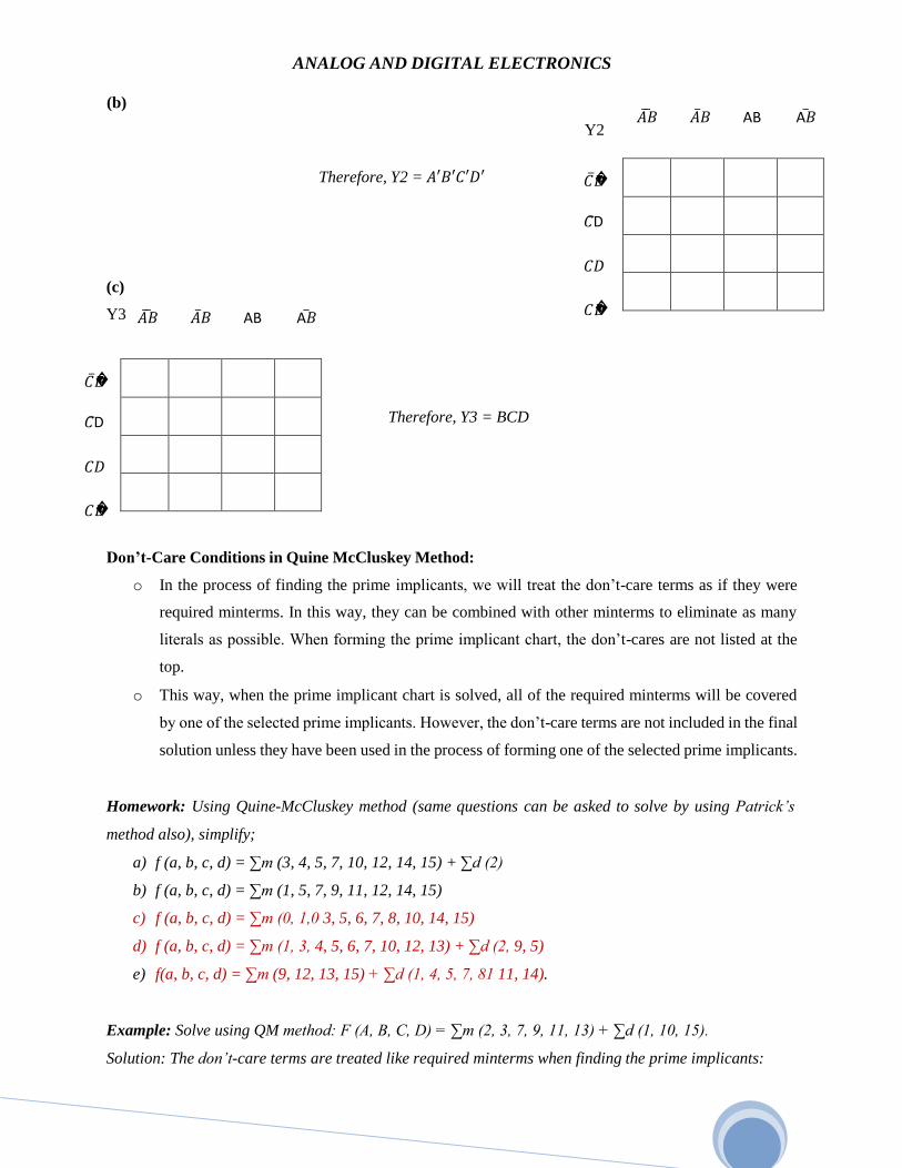
27
18CS33
(b)
ANALOG AND DIGITAL ELECTRONICS
Y2
𝐴 𝐵 𝐴 𝐵 AB A𝐵
Therefore, Y2 = 𝐴′𝐵′𝐶′𝐷′ 𝐶 𝐷
𝐶 D
(c)
Y3
𝐴 𝐵 𝐴 𝐵 AB A𝐵
𝐶𝐷
𝐶𝐷
𝐶 𝐷
𝐶 D
𝐶𝐷
𝐶𝐷
Therefore, Y3 = BCD
Don’t-Care Conditions in Quine McCluskey Method:
o In the process of finding the prime implicants, we will treat the don’t-care terms as if they were
required minterms. In this way, they can be combined with other minterms to eliminate as many
literals as possible. When forming the prime implicant chart, the don’t-cares are not listed at the
top.
o This way, when the prime implicant chart is solved, all of the required minterms will be covered
by one of the selected prime implicants. However, the don’t-care terms are not included in the final
solution unless they have been used in the process of forming one of the selected prime implicants.
Homework: Using Quine-McCluskey method (same questions can be asked to solve by using Patrick’s
method also), simplify;
a) f (a, b, c, d) = ∑m (3, 4, 5, 7, 10, 12, 14, 15) + ∑d (2)
b) f (a, b, c, d) = ∑m (1, 5, 7, 9, 11, 12, 14, 15)
c) f (a, b, c, d) = ∑m (0, 1,0 3, 5, 6, 7, 8, 10, 14, 15)
d) f (a, b, c, d) = ∑m (1, 3, 4, 5, 6, 7, 10, 12, 13) + ∑d (2, 9, 5)
e) f(a, b, c, d) = ∑m (9, 12, 13, 15) + ∑d (1, 4, 5, 7, 81 11, 14).
Example: Solve using QM method: F (A, B, C, D) = ∑m (2, 3, 7, 9, 11, 13) + ∑d (1, 10, 15).
Solution: The don’t-care terms are treated like required minterms when finding the prime implicants:

28
18CS33
ANALOG AND DIGITAL ELECTRONICS
The don’t-care columns are omitted when forming the prime implicant chart:
- 2 3 7 9 11 13
Therefore, F =
SIMPLIFICATION USING MAP-ENTERED VARIABLES:
Although the Quine-McCluskey method can be used with functions with a fairly large number of variables,
it is not very efficient for functions that have many variables and relatively few terms. Some of these
functions can be simplified by using a modification of the Karnaugh map method. By using map- entered
variables, Karnaugh map techniques can be extended to simplify functions with more than four or five
variables. The following Figure shows a four-variable map with two additional variables entered in the
squares in the map.
A B C D F
0 0 0 0
0 0 0 1
0 0 1 0
0 0 1 1
0 1 0 0
0 1 0 1
0 1 1 0
0 1 1 1
1 0 0 0
1 0 0 1
1 0 1 0
1 0 1 1
1 1 0 0
1 1 0 1
1 1 1 0
1 1 1 1
Column 1
ABCD
Column 2
ABCD
Column 3
ABCD
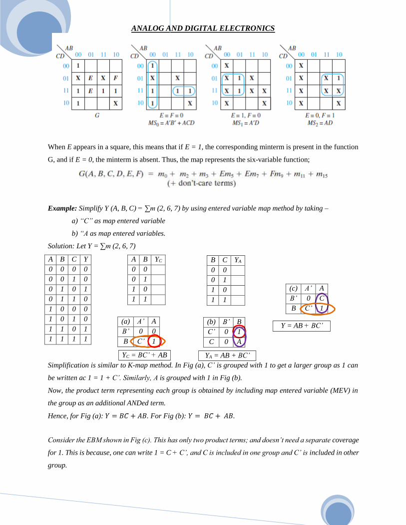
29
ANALOG AND DIGITAL ELECTRONICS
When E appears in a square, this means that if E = 1, the corresponding minterm is present in the function
G, and if E = 0, the minterm is absent. Thus, the map represents the six-variable function;
Example: Simplify Y (A, B, C) = ∑m (2, 6, 7) by using entered variable map method by taking –
a) “C” as map entered variable
b) “A as map entered variables.
Solution: Let Y = ∑m (2, 6, 7)
Simplification is similar to K-map method. In Fig (a), C’ is grouped with 1 to get a larger group as 1 can
be written ac 1 = 1 + C’. Similarly, A is grouped with 1 in Fig (b).
Now, the product term representing each group is obtained by including map entered variable (MEV) in
the group as an additional ANDed term.
Hence, for Fig (a): 𝑌 = 𝐵𝐶 + 𝐴𝐵. For Fig (b): 𝑌 = 𝐵𝐶 + 𝐴𝐵.
Consider the EBM shown in Fig (c). This has only two product terms; and doesn’t need a separate coverage
for 1. This is because, one can write 1 = C + C’, and C is included in one group and C’ is included in other
group.
A B C Y
0 0 0 0
0 0 1 0
0 1 0 1
0 1 1 0
1 0 0 0
1 0 1 0
1 1 0 1
1 1 1 1
A B YC
0 0
0 1
1 0
1 1
B C YA
0 0
0 1
1 0
1 1
(c) A’ A
B’ 0 C
B C’ 1
Y = AB + BC’
(a) A’ A
B’ 0 0
B C’ 1
(b) B’ B
C’ 0 1
C 0 A
YC = BC’ + AB YA = AB + BC’
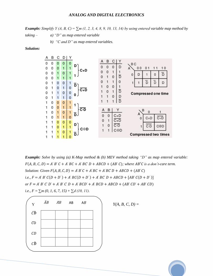
30
Y 𝐴 𝐵 𝐴 𝐵 AB A𝐵
𝐶 𝐷
𝐶 D
𝐶𝐷
𝐶𝐷
18CS33
ANALOG AND DIGITAL ELECTRONICS
Example: Simplify Y (A, B, C) = ∑m (1, 2, 3, 4, 8, 9, 10, 13, 14) by using entered variable map method by
taking – a) “D” as map entered variable
b) “C and D” as map entered variables.
Solution:
Example: Solve by using (a) K-Map method & (b) MEV method taking “D” as map entered variable:
𝐹(𝐴, 𝐵, 𝐶, 𝐷) = 𝐴′ 𝐵′ 𝐶 + 𝐴′ 𝐵𝐶 + 𝐴′ 𝐵𝐶′ 𝐷 + 𝐴𝐵𝐶𝐷 + (𝐴𝐵′ 𝐶); where 𝐴𝐵′𝐶 is a don’t-care term.
Solution: Given 𝐹(𝐴, 𝐵, 𝐶, 𝐷) = 𝐴′ 𝐵′ 𝐶 + 𝐴′ 𝐵𝐶 + 𝐴′ 𝐵𝐶′ 𝐷 + 𝐴𝐵𝐶𝐷 + (𝐴𝐵′ 𝐶)
i.e., 𝐹 = 𝐴′ 𝐵′ 𝐶(𝐷 + 𝐷′ ) + 𝐴′ 𝐵𝐶(𝐷 + 𝐷′ ) + 𝐴′ 𝐵𝐶′ 𝐷 + 𝐴𝐵𝐶𝐷 + [𝐴𝐵′ 𝐶(𝐷 + 𝐷′ )]
or 𝐹 = 𝐴′ 𝐵′ 𝐶′ 𝐷′ + 𝐴′ 𝐵′ 𝐶′ 𝐷 + 𝐴′ 𝐵𝐶𝐷′ + 𝐴′ 𝐵𝐶𝐷 + 𝐴𝐵𝐶𝐷 + (𝐴𝐵′ 𝐶𝐷′ + 𝐴𝐵′ 𝐶𝐷)
i.e., F = ∑m (0, 1, 6, 7, 15) + ∑d (10, 11).
Y(A, B, C, D) =
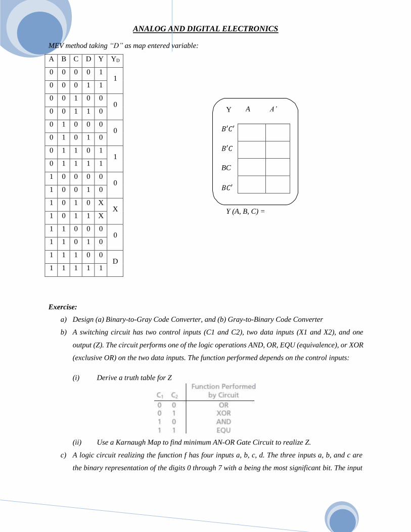
31
Y A A’
𝐵′𝐶′
𝐵′𝐶
BC
𝐵𝐶′
ANALOG AND DIGITAL ELECTRONICS
MEV method taking “D” as map entered variable:
Y (A, B, C) =
Exercise:
a) Design (a) Binary-to-Gray Code Converter, and (b) Gray-to-Binary Code Converter
b) A switching circuit has two control inputs (C1 and C2), two data inputs (X1 and X2), and one
output (Z). The circuit performs one of the logic operations AND, OR, EQU (equivalence), or XOR
(exclusive OR) on the two data inputs. The function performed depends on the control inputs:
(i) Derive a truth table for Z
(ii) Use a Karnaugh Map to find minimum AN-OR Gate Circuit to realize Z.
c) A logic circuit realizing the function f has four inputs a, b, c, d. The three inputs a, b, and c are
the binary representation of the digits 0 through 7 with a being the most significant bit. The input
A B C D Y YD
0 0 0 0 1 1
0 0 0 1 1
0 0 1 0 0 0
0 0 1 1 0
0 1 0 0 0 0
0 1 0 1 0
0 1 1 0 1 1
0 1 1 1 1
1 0 0 0 0 0
1 0 0 1 0
1 0 1 0 X X
1 0 1 1 X
1 1 0 0 0 0
1 1 0 1 0
1 1 1 0 0 D
1 1 1 1 1

32
18CS33
ANALOG AND DIGITAL ELECTRONICS
d is an odd-parity bit; that is, the value of d is such that a, b, c, and d always contains an odd
number of 1’s. (For example, the digit 1 is represented by abc = 001 and d = 0, and the digit 3 is
represented by abcd = 0111.) The function f has value 1 if the input digit is a prime number. (A
number is prime if it is divisible only by itself and 1; 1 is considered to be prime, and 0 is not.)
a. Draw a Karnaugh map for f
b. Find all prime implicants of f
c. Find all minimum sum of products for f
d. Find all prime implicants of f’
e. Find all minimum product of sums for f.
Try these: Design a minimal sum combinational circuit to –
a) Find the 9s complement of BCD numbers
b) Convert BCD to Excess-3
c) Multiply two 2-bit numbers
d) Output a 1 when an illegal BCD code occurs
e) Output the 2s complement of a 4-bit binary number.
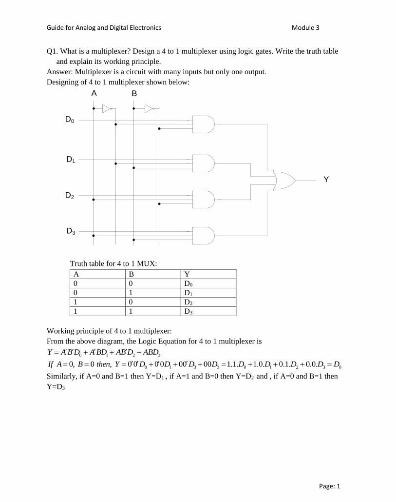
Guide for Analog and Digital Electronics Module 3
Page: 1
Q1. What is a multiplexer? Design a 4 to 1 multiplexer using logic gates. Write the truth table
and explain its working principle.
Answer: Multiplexer is a circuit with many inputs but only one output.
Designing of 4 to 1 multiplexer shown below:
D0
D1
D2
D3
Y
A B
Truth table for 4 to 1 MUX:
A B Y
0 0 D0
0 1 D1
1 0 D2
1 1 D3
Working principle of 4 to 1 multiplexer:
From the above diagram, the Logic Equation for 4 to 1 multiplexer is
0 1 2 3
0 1 3 3 0 1 2 3 0 0, 0 , 0 0 0 0 00 00 1.1. 1.0. 0.1. 0.0.
Y A B D A BD AB D ABD
If A B then Y D D D D D D D D D
Similarly, if A=0 and B=1 then Y=D1 , if A=1 and B=0 then Y=D2 and , if A=0 and B=1 then
Y=D3
PDF Watermark Remover DEMO : Purchase from www.PDFWatermarkRemover.com to remove the watermark

Guide for Analog and Digital Electronics Module 3
Page: 2
Q2. Construct 4:1 multiplexer using only 2:1 multiplexer.
Answer: 0 1 2 :1 Logic Equation for Multiplexer is Y A D AD
0 1 2 3
0 1 2 3
4 :1
( ) ( )
Logic equation for Multplexer is Y A B D A BD AB D ABD
Y A B D BD A B D BD
We require three 2:1 Multiplexers and the connection is shown below.
D0
D1
D2
D3
B
B
A
Y
2:1
Multiplexer
2:1
Multiplexer
2:1
Multiplexer
Q3. Construct 8:1 multiplexer using only 2:1 multiplexer.
Answer: 0 1 2 :1 Logic Equation for Multiplexer is Y A D AD
0 1 2 3 4 5 6 7
0 1 2 3 4 5 6 7
0 1 2 3 4
8 :1
( ) ( )
[ ( ) ( )] [ (
Logic Equation for Multiplexer is
Y A B C D A B CD A BC D A BCD AB C D AB CD ABC D ABCD
Y A B C D B CD BC D BCD A B C D B CD BC D BCD
Y A B C D CD B C D CD A B C D CD
5 6 7) ( )]B C D CD
PDF Watermark Remover DEMO : Purchase from www.PDFWatermarkRemover.com to remove the watermark

Guide for Analog and Digital Electronics Module 3
Page: 3
D0
D1
D2
D3
C
C
B2:1
Multiplexer
2:1
Multiplexer
2:1
Multiplexer
D4
D5
D6
D7
C
C
B2:1
Multiplexer
2:1
Multiplexer
2:1
Multiplexer
2:1
MultiplexerY
A
Q4. Design 16 to 1 multiplexer using 8 to 1 multiplexer and one 2 to 1 multiplexer.
Answer: 0 1 2 :1 Logic Equation for Multiplexer is Y A D AD
0 1 2 3 4 5 6 7
8 :1 Logic Equation for Multiplexer is
Y A B C D A B CD A BC D A BCD AB C D AB CD ABC D ABCD
0 1 6 7 8 9 14 15
0 1 6 7 8 9 14 15
16 :1
... ...
( ... ) ( ... )
Logic Equation for Multiplexer is
Y A B C D D A B C DD A BCD D A BCDD AB C D AB C D ABCD D ABCDD
Y A B C D D B C DD BCD D BCDD A B C D B C D BCD D BCDD
PDF Watermark Remover DEMO : Purchase from www.PDFWatermarkRemover.com to remove the watermark

Guide for Analog and Digital Electronics Module 3
Page: 4
D0
D7
D8
D15
B
B
A
Y
8:1
Multiplexer
8:1
Multiplexer
2:1
Multiplexer
C D
C D
Q5. Design 32 to 1 multiplexer using 16 to 1 multiplexer and one 2 to 1 multiplexer.
Answer: 0 1 2 :1 Logic Equation for Multiplexer is Y A D AD
0 1 14 15
16 :1
.....
Logic Equation for Multiplexer is
Y A B C D D A B C DD ABCD D ABCDD
0 14 15 16 30 31
0 14 15 16 30 31
32 :1
... ...
( ... ) ( ... )
Logic Equation for Multiplexer is
Y A B C D E D A BCDE D A BCDED AB C D E D ABCDE D ABCDED
Y A B C D E D BCDE D BCDED A B C D E D BCDE D BCDED
D0
D15
D16
D31
B
B
A
Y
16:1
Multiplexer
16:1
Multiplexer
2:1
Multiplexer
C D
C D
E
E
PDF Watermark Remover DEMO : Purchase from www.PDFWatermarkRemover.com to remove the watermark

Guide for Analog and Digital Electronics Module 3
Page: 5
Q6. Mention the differences between decoder and demultiplexer.
Answer:
Demultiplexer Decoder
There is one data input and multiple output.
There are selects used as control bits.
There is no data input. The only inputs are the
control bit.
The data input appears at one of the output as
per the control inputs.
One of the output is high as per the control
inputs.
Input appears at the output where subscription
of the output is equal to the decimal equivalent
to the inputs.
Output becomes high where subscription of the
output is equal to the decimal equivalent to the
inputs
Q7. (a) Realize Y A B B C ABC using an 8 to 1 Multiplexer.
(b) Can it be realized with a 4 to 1 multiplxer?
0 1 2 3 4 5 6 7
: ( ) 8 :1 Answer a Logic Equation for Multiplexer is
Y A B C D A B CD A BC D A BCD AB C D AB CD ABC D ABCD
We should express Y as a function of three variables i.e function of minterms.
( ) ( )
Y A B B C ABC
Y A B C C B C A A ABC
Y A BC A BC AB C A B C ABC
Y A B C A BC A BC AB C ABC
Comparing with the Logic equation of 8:1 Multiplexer, we have
0 2 3 4 7 1 5 61 0D D D D D and D D D
A B C
D0=1D1=0D2=1D3=1D4=1D5=0D6=0
D7=1
Y8:1
Multiplexer
( )
( )
. .1 . .
b Y A B B C ABC
Y A B B C A A ABC
Y A B AB C A B C ABC
Y A B C A B AB C AB C
0 1 2 3 4 :1 Logic equation for Multplexer is Y A B D A BD AB D ABD
PDF Watermark Remover DEMO : Purchase from www.PDFWatermarkRemover.com to remove the watermark

Guide for Analog and Digital Electronics Module 3
Page: 6
0 1 2 3 , , 1, We have D C D D C and D C
A B
D0=Cʹ
D1=1
D2=Cʹ
D3=C
Y4:1
Multiplexer
Q8. Implement the following Boolean functions using 4:1 multiplexer (MUX):
( ) ( , , , ) (0,1,2,4,6,9,12,14)
( ) ( , , ) (1,3,5,6)
i Y f A B C D m
ii F A B C m
Answer: 0 1 2 3 4 :1 Logic equation for Multplexer is Y A B D A BD AB D ABD
( , , , ) (0,1,2,4,6,9,12,14)
( ) ( ) ( )
4 :1 ,
Y f A B C D m
Y A B C D A B C D A B CD A BC D A BCD AB C D ABC D ABCD
Y A B C D C D CD A B C D CD AB C D AB C D CD
Comparing with Logic Equation of Multiplexer
0 0
1 1
2 2
3 3
.1 .1 .1 .0
.1 .0 .1 .0
.0 .1 .0 .0
.1 .0 .1 .0
We have
D C D C D CD D C D C D CD CD
D C D CD D C D C D CD CD
D C D D C D C D CD CD
D C D CD D C D C D CD CD
PDF Watermark Remover DEMO : Purchase from www.PDFWatermarkRemover.com to remove the watermark
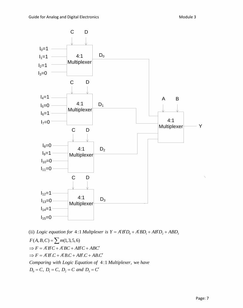
Guide for Analog and Digital Electronics Module 3
Page: 7
4:1
Multiplexer
4:1
Multiplexer
4:1
Multiplexer
4:1
Multiplexer
4:1
Multiplexer
C D
C D
C D
C D
A B
I0=1
I1=1
I2=1
I3=0
I4=1
I5=0
I6=1
I7=0
I8=0
I9=1
I10=0
I11=0
I12=1
I13=0
I14=1
I15=0
D0
D1
D2
D3
Y
(ii) 0 1 2 3 4 :1 Logic equation for Multplexer is Y A B D A BD AB D ABD
0 1 2 3
( , , ) (1,3,5,6)
. . . .
4 :1 , we
, ,
F A B C m
F A B C A BC AB C ABC
F A B C A B C AB C AB C
Comparing with Logic Equation of Multiplexer have
D C D C D C and D C
PDF Watermark Remover DEMO : Purchase from www.PDFWatermarkRemover.com to remove the watermark
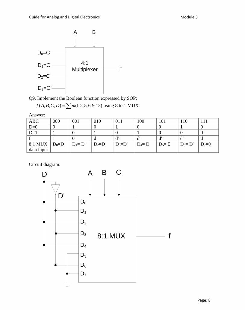
Guide for Analog and Digital Electronics Module 3
Page: 8
A B
D0=C
D1=C
D2=C
D3=Cʹ
F4:1
Multiplexer
Q9. Implement the Boolean function expressed by SOP:
( , , , ) (1,2,5,6,9,12) using 8 to 1 MUX.f A B C D m
Answer:
ABC 000 001 010 011 100 101 110 111
D=0 0 1 0 1 0 0 1 0
D=1 1 0 1 0 1 0 0 0
f 1 0 d d' d' d' d' d
8:1 MUX
data input
D0=D D1= D' D2=D D3=D' D4= D D5= 0 D6= D' D7=0
Circuit diagram:
A B CD
D0
D1
D2
D3
D4
D5
D6
D7
f8:1 MUX
D'
PDF Watermark Remover DEMO : Purchase from www.PDFWatermarkRemover.com to remove the watermark

Guide for Analog and Digital Electronics Module 3
Page: 9
Q10. Implement the Boolean function:
( , , , ) (0,1,2,4,5,7,8,9)F A B C D m using 8 to 1 multiplexers. Draw the logic diagram and
explain the operation. Additional gates can be used if required.
0 1 2 3 4 5 6 7
: ( ) 8 :1 Answer a Logic Equation for Multiplexer is
Y A B C D A B CD A BC D A BCD AB C D AB CD ABC D ABCD
0 1 2 :1 Logic Equation for Multiplexer is Y A D AD
0
( , , , ) (0,1,2,4,5,7,8,9)
( ) ( )
2 :1 ,
F A B C D m
F A B C D A B C D A B CD A BC D A BC D A BCD AB C D AB C D
F A B C D B C D B CD BC D BC D BCD A B C D B C D
Comparing with Logic Equation we have
D B C D
0
1
1
.1 .1 .1 .0 .1 .0 .0 .1
.1 .1 .0 .0 .0 .0 .0 .0
B C D B CD BC D BC D BCD
D B C D B C D B CD B CD BC D BC D BCD BCD
D B C D B C D
D B C D B C D B CD B CD BC D BC D BCD BCD
A
Aʹ
B C D
B C DF
D0
D1
I0=1I1=1
I2=1
I3=0I4=1
I5=1
I6=0I7=1
I8=1
I9=1I10=0I11=0
I12=0
I13=0
I14=0
I15=0
8:1
Multiplxer
8:1
Multiplxer
(Note: Q9 and Q10 are similar. But method for Q9 is preferable)
PDF Watermark Remover DEMO : Purchase from www.PDFWatermarkRemover.com to remove the watermark
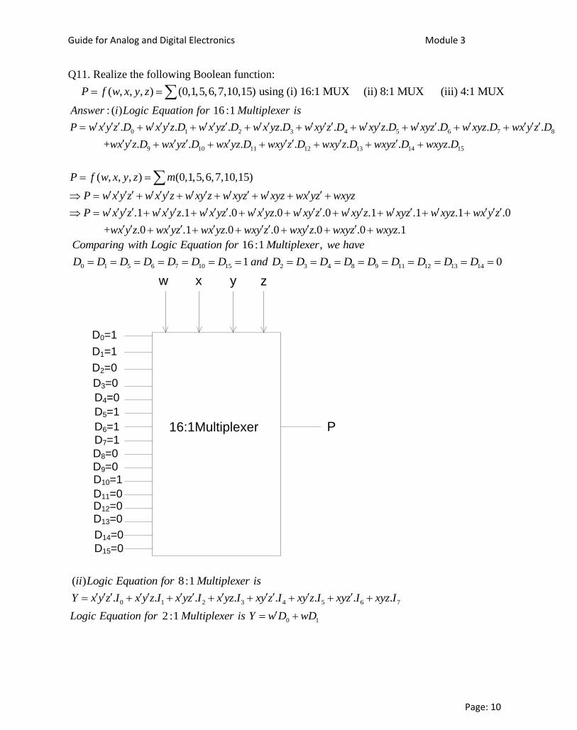
Guide for Analog and Digital Electronics Module 3
Page: 10
Q11. Realize the following Boolean function:
( , , , ) (0,1,5,6,7,10,15) using (i) 16:1 MUX (ii) 8:1 MUX (iii) 4:1 MUXP f w x y z
0 1 2 3 4 5 6 7 8
9 10 11 12
: ( ) 16 :1
. . . . . . . . .
+ . . . .
Answer i Logic Equation for Multiplexer is
P w x y z D w x y z D w x yz D w x yz D w xy z D w xy z D w xyz D w xyz D wx y z D
wx y z D wx yz D wx yz D wxy z D w
13 14 15. . .xy z D wxyz D wxyz D
( , , , ) (0,1,5,6,7,10,15)
.1 .1 .0 .0 .0 .1 .1 .1 .0
+ .0 .
P f w x y z m
P w x y z w x y z w xy z w xyz w xyz wx yz wxyz
P w x y z w x y z w x yz w x yz w xy z w xy z w xyz w xyz wx y z
wx y z wx yz
1 .0 .0 .0 .0 .1wx yz wxy z wxy z wxyz wxyz
0 1 5 6 7 10 15 2 3 4 8 9 11 12 13 14
16 :1 ,
1 0
Comparing with Logic Equation for Multiplexer we have
D D D D D D D and D D D D D D D D D
D0=1
D1=1
D2=0
D3=0
D4=0
D5=1
D6=1D7=1
D8=0D9=0D10=1
D11=0D12=0D13=0
D14=0
D15=0
w x y z
P16:1Multiplexer
0 1 2 3 4 5 6 7
( ) 8 :1
. . . . . . . .
ii Logic Equation for Multiplexer is
Y x y z I x y z I x yz I x yz I xy z I xy z I xyz I xyz I
0 1 2 :1 Logic Equation for Multiplexer is Y w D wD
PDF Watermark Remover DEMO : Purchase from www.PDFWatermarkRemover.com to remove the watermark

Guide for Analog and Digital Electronics Module 3
Page: 11
( , , , ) (0,1,5,6,7,10,15)
( ) ( )
( .1 .1 .0 .0 .0 .1 .1 .1)
P f w x y z m
P w x y z w x y z w xy z w xyz w xyz wx yz wxyz
P w x y z x y z xy z xyz xyz w x yz xyz
P w x y z x y z x yz x yz xy z xy z xyz xyz
0
1
( .0 .0 .1 .0 .0 .0 .0 .1)
2:1 ,
.1 .1 .0 .0 .0 .1 .1 .1
.0
w x y z x y z x yz x yz xy z xy z xyz xyz
Comparing with Logic Equation of Multiplexer we have
D x y z x y z x yz x yz xy z xy z xyz xyz
D x y z
.0 .1 .0 .0 .0 .0 .1x y z x yz x yz xy z xy z xyz xyz
w
wʹ
x y z
x y zP
D0
D1
I0=1I1=1
I2=0
I3=0I4=0
I5=1
I6=1I7=1
I8=0
I9=0I10=1I11=0
I12=0
I13=0
I14=0
I15=1
8:1
Multiplxer
8:1
Multiplxer
PDF Watermark Remover DEMO : Purchase from www.PDFWatermarkRemover.com to remove the watermark

Guide for Analog and Digital Electronics Module 3
Page: 12
(iii) 0 1 2 3 4 :1 Logic equation for Multplexer is Y w x D w xD wx D wxD
0 0
( , , , ) (0,1,5,6,7,10,15)
( ) ( )
4:1 ,
P f w x y z m
P w x y z w x y z w xy z w xyz w xyz wx yz wxyz
P w x y z y z w x y z yz yz wx yz wxyz
Comparing with Logic Equation for Multiplexer we have
D y z y z D
1 1
2
3
.1 .1 .0 .0
.0 .1 .1 .1
.0 .0 .1 .0
.0 .0 .0 .1
y z y z yz yz
D y z yz yz D y z y z yz yz
D yz y z y z yz yz
D yz y z y z yz yz
4:1
Multiplexer
4:1
Multiplexer
4:1
Multiplexer
4:1
Multiplexer
4:1
Multiplexer
y z
y z
y z
y z
w x
I0=1
I1=1
I2=0
I3=0
I4=0
I5=1
I6=1
I7=1
I8=0
I9=0
I10=1
I11=0
I12=0
I13=0
I14=0
I15=1
D0
D1
D2
D3
P
PDF Watermark Remover DEMO : Purchase from www.PDFWatermarkRemover.com to remove the watermark
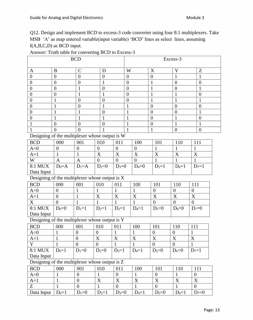
Guide for Analog and Digital Electronics Module 3
Page: 13
Q12. Design and implement BCD to excess-3 code converter using four 8:1 multiplexers. Take
MSB ‘A’ as map entered variable(input variable) ‘BCD’ lines as select lines, assuming
f(A,B,C,D) as BCD input.
Answer: Truth table for converting BCD to Excess-3
BCD
Excess-3
A B C D W X Y Z
0 0 0 0 0 0 1 1
0 0 0 1 0 1 0 0
0 0 1 0 0 1 0 1
0 0 1 1 0 1 1 0
0 1 0 0 0 1 1 1
0 1 0 1 1 0 0 0
0 1 1 0 1 0 0 1
0 1 1 1 1 0 1 0
1 0 0 0 1 0 1 1
1 0 0 1 1 1 0 0
Designing of the multiplexer whose output is W
BCD 000 001 010 011 100 101 110 111
A=0 0 0 0 0 0 1 1 1
A=1 1 1 X X X X X X
W A A 0 0 0 1 1 1
8:1 MUX
Data Input
D0=A D1=A D2=0 D3=0 D4=0 D5=1 D6=1 D7=1
Designing of the multiplexer whose output is X
BCD 000 001 010 011 100 101 110 111
A=0 0 1 1 1 1 0 0 0
A=1 0 1 X X X X X X
X 0 1 1 1 1 0 0 0
8:1 MUX
Data Input
D0=0 D1=1 D2=1 D3=1 D4=1 D5=0 D6=0 D7=0
Designing of the multiplexer whose output is Y
BCD 000 001 010 011 100 101 110 111
A=0 1 0 0 1 1 0 0 1
A=1 1 0 X X X X X X
Y 1 0 0 1 1 0 0 1
8:1 MUX
Data Input
D0=1 D1=0 D2=0 D3=1 D4=1 D5=0 D6=0 D7=1
Designing of the multiplexer whose output is Z
BCD 000 001 010 011 100 101 110 111
A=0 1 0 1 0 1 0 1 0
A=1 1 0 X X X X X X
Z 1 0 1 0 1 0 1 0
Data Input D0=1 D1=0 D2=1 D3=0 D4=1 D5=0 D6=1 D7=0
PDF Watermark Remover DEMO : Purchase from www.PDFWatermarkRemover.com to remove the watermark

Guide for Analog and Digital Electronics Module 3
Page: 14
D0D1D2D3D4D5D6D7
B C D
D0D1D2D3D4D5D6D7
B C D
D0D1D2D3D4D5D6D7
B C D
D0D1D2D3D4D5D6D7
B C D
W
X
Y
Z
AA
000111
011
1
100
0
1
00
1100
1
10
10
101
0
8:1
Multiplexer
8:1
Multiplexer
8:1
Multiplexer
8:1
Multiplexer
PDF Watermark Remover DEMO : Purchase from www.PDFWatermarkRemover.com to remove the watermark
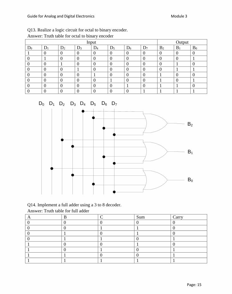
Guide for Analog and Digital Electronics Module 3
Page: 15
Q13. Realize a logic circuit for octal to binary encoder.
Answer: Truth table for octal to binary encoder
Input Output
D0 D1 D2 D3 D4 D5 D6 D7 B2 B1 B0
1 0 0 0 0 0 0 0 0 0 0
0 1 0 0 0 0 0 0 0 0 1
0 0 1 0 0 0 0 0 0 1 0
0 0 0 1 0 0 0 0 0 1 1
0 0 0 0 1 0 0 0 1 0 0
0 0 0 0 0 1 0 0 1 0 1
0 0 0 0 0 0 1 0 1 1 0
0 0 0 0 0 0 0 1 1 1 1
D0 D1 D2 D3 D4 D5 D6 D7
B2
B1
B0
Q14. Implement a full adder using a 3 to 8 decoder.
Answer: Truth table for full adder
A B C Sum Carry
0 0 0 0 0
0 0 1 1 0
0 1 0 1 0
0 1 1 0 1
1 0 0 1 0
1 0 1 0 1
1 1 0 0 1
1 1 1 1 1
PDF Watermark Remover DEMO : Purchase from www.PDFWatermarkRemover.com to remove the watermark
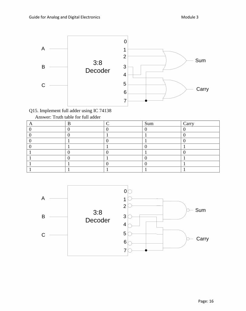
Guide for Analog and Digital Electronics Module 3
Page: 16
0
1
2
3
4
5
6
7
Sum
Carry
A
B
C
3:8
Decoder
Q15. Implement full adder using IC 74138
Answer: Truth table for full adder
A B C Sum Carry
0 0 0 0 0
0 0 1 1 0
0 1 0 1 0
0 1 1 0 1
1 0 0 1 0
1 0 1 0 1
1 1 0 0 1
1 1 1 1 1
0
1
2
3
4
5
6
7
Sum
Carry
A
B
C
3:8
Decoder
PDF Watermark Remover DEMO : Purchase from www.PDFWatermarkRemover.com to remove the watermark

Guide for Analog and Digital Electronics Module 3
Page: 17
Q16. Implement 3 bit binary to gray code conversion by using IC 74139.
Answer: Truth table for converting 3 bit binary to gray code
Binary code Gray code
A B C X Y Y
0 0 0 0 0 0
0 0 1 0 0 1
0 1 0 0 1 1
0 1 1 0 1 0
1 0 0 1 1 0
1 0 1 1 1 1
1 1 0 1 0 1
1 1 1 1 0 0
00
01
11
10
0 1ABC
00
01
11
10
0 1ABC
00
01
11
10
0 1ABC
K-Map for X: K-Map for Y: K-Map for Z:
0 0
0 0
1 1
1 1
0 0
1 1
0 0
1 1
0 1
1 0
1 0
0 1
X=A Y=AB+AB Z=BC+BC
A
B
C
X
Y
Z
74139
74139
PDF Watermark Remover DEMO : Purchase from www.PDFWatermarkRemover.com to remove the watermark

Guide for Analog and Digital Electronics Module 3
Page: 18
Q17. Design a priority encoder for a system with a 3 inputs, the middle bit with highest priority
encoding to 10, the MSB with the next priority encoding to 11, while the LSB with least priority
encoding to 01.
Answer: Truth table of the priority encoder
Input Output
A B C X Y
0 0 0 0 0
0 0 1 0 1
0 1 0 1 0
0 1 1 1 0
1 0 0 1 1
1 0 1 1 1
1 1 0 1 0
1 1 1 1 0
K-Map for X:
ABC
00
01
11
10
0 1
0 0
1 1
1 1
1 1
K-Map for Y:
ABC
00
01
11
10
0 1
0 1
0 0
0 0
1 1
X=A+B Y=AB+BC=B(A+C)
A B C
X
Y
PDF Watermark Remover DEMO : Purchase from www.PDFWatermarkRemover.com to remove the watermark

Guide for Analog and Digital Electronics Module 3
Page: 19
Q18. Design a 4 to 16 line decoder using 2 to 4 line decoder which has the active low outputs as
active low enable input. Explain its operation.
Answer:
2 to 4 line
decoder
2 to 4 line
decoder
2 to 4 line
decoder
2 to 4 line
decoder
2 to 4 line
decoder
C
D
A
B
E
E
E
E
Q19. Write the comparisons between PLA and PAL.
Answer:
PAL PLA
The output OR-gate array is fixed while the
input AND gate array is fusible linked and thus
programmable.
Both output OR-gate array and input AND gate
array are fusible linked.
PAL is easier to program. PLA is more complicated since the number
fusible links are more compared to PAL
PAL is less expensive. PLA is more expensive compared to PAL.
PDF Watermark Remover DEMO : Purchase from www.PDFWatermarkRemover.com to remove the watermark

Guide for Analog and Digital Electronics Module 3
Page: 20
Q20. Design 7-segments decoder using PLA.
Answer: Seven segment indicator:
a
b
c
d
e
f
g
Following table shows the segments should light up to display a number.
Number to display Segments to light up
0 a,b,c,d,e,f
1 b,c
2 a,b,d,e,g
3 a,b,c.d,g
4 b,c,f,g
5 a,c,d,f
6 a,c,d,e,f,g
7 a,b,c
8 a,b,c,d,e,f,g
9 a,b,c,f,g
PDF Watermark Remover DEMO : Purchase from www.PDFWatermarkRemover.com to remove the watermark
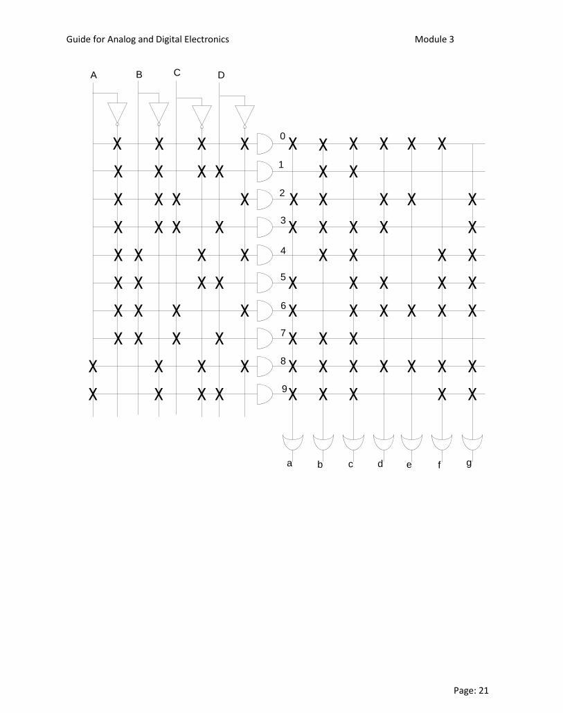
Guide for Analog and Digital Electronics Module 3
Page: 21
χ χ χ χ
χ χ χ χ
χ χ χ χ
χ χ χ χ
χ χ χ χ
χ χ χ χ
χ χ χ χ
χ χ χ χ
χ χ χ χ
χ χ χ χ
0
1
2
3
4
5
6
7
8
9
χ χ
χ
χ
χ
χ
χ
χ
χ
χ
χ
χ
χ
χ
χ
χ
χ
χ
χ
χ
χ
χ
χ
χ
χ
χ
χ
χ
χ
χ
χ
χ
χ
χ
χ
χ
χ
χ
χ
χ
χ
χ
χ
χ
χ
χ
χ
χ
a b c d e f g
A B C D
PDF Watermark Remover DEMO : Purchase from www.PDFWatermarkRemover.com to remove the watermark

Guide for Analog and Digital Electronics Module 3
Page: 22
Q21. Implement the following function using PLA:
A(x,y,z)=Σm(1,2,3,6); B(x,y,z)=Σm(0,1,6,7); C(x,y,z)=Σm(2,6)
Answer:
0
1
2
3
4
5
6
7
A B C
A(x,y,z)
=Σm(1,2,3,6)
B(x,y,z)
=Σm(0,1,6,7)A(x,y,z)
=Σm(,2,6)
χ χ χ
χ χ χ
χ χ χ
χ χ χ
χ χ χ
χ χ χ
χ χ χ
χ χ χ
χ
χ
χ
χ
χ
χ
χ
χ
χ
χ
PDF Watermark Remover DEMO : Purchase from www.PDFWatermarkRemover.com to remove the watermark
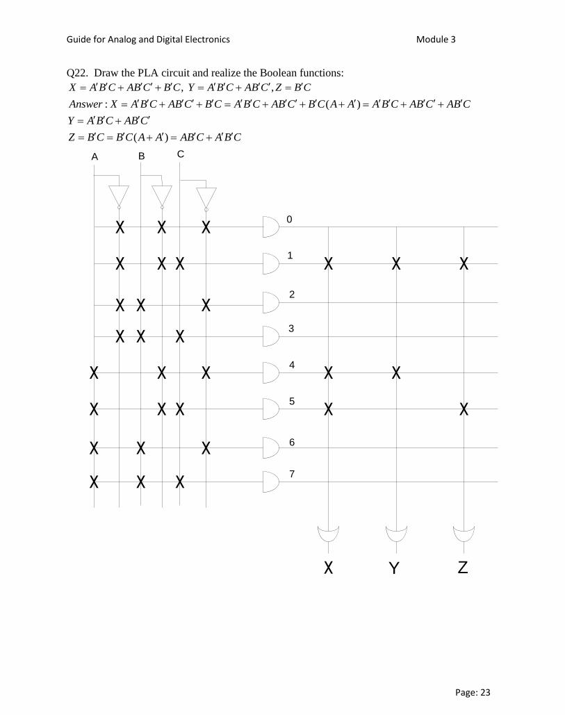
Guide for Analog and Digital Electronics Module 3
Page: 23
Q22. Draw the PLA circuit and realize the Boolean functions:
, ,X A B C AB C B C Y A B C AB C Z B C
: ( )
( )
Answer X A B C AB C B C A B C AB C B C A A A B C AB C AB C
Y A B C AB C
Z B C B C A A AB C A B C
0
1
2
3
4
5
6
7
A B C
χ χ χ
χ χ χ
χ χ χ
χ χ χ
χ χ χ
χ χ χ
χ χ χ
χ χ χ
χ χ
χ
χ
χ
χ
χ
χ Y Z
PDF Watermark Remover DEMO : Purchase from www.PDFWatermarkRemover.com to remove the watermark

Guide for Analog and Digital Electronics Module 3
Page: 24
Q23. Describe the working principle of 3:8 decoder. Design a circuit that realizes the following
functions using a 3:8 decoder and multi input OR gates.
1 2( ) ( , , ) (1,3,7) (ii) ( , , ) (2,3,5)i F A B C m F A B C m
Answer: Working principle of 3:8 decoder:
There are 3 inputs and 8 outputs in a 3:8 decoder. One of the output is HIGH and remaining
seven are LOW according to inputs. This is shown in truth table.
ABC
ABC
ABC
ABC
ABC
ABC
ABC
ABC
A B C
3:8 Decoder
Y0
Y1
Y2
Y3
Y4
Y5
Y6
Y7
Truth table of 3:8 Decoder :
A B C Y0 Y1 Y2 Y3 Y4 Y5 Y6 Y7
0 0 0 1 0 0 0 0 0 0 0
0 0 0 0 1 0 0 0 0 0 0
0 1 0 0 0 1 0 0 0 0 0
0 1 1 0 0 0 1 0 0 0 0
1 0 0 0 0 0 0 1 0 0 0
1 0 1 0 0 0 0 0 1 0 0
1 1 0 0 0 0 0 0 0 1 0
1 1 1 0 0 0 0 0 0 0 1
PDF Watermark Remover DEMO : Purchase from www.PDFWatermarkRemover.com to remove the watermark

Guide for Analog and Digital Electronics Module 3
Page: 25
ABC
ABC
ABC
ABC
ABC
ABC
ABC
ABC
A B C
3:8 Decoder
Y0
Y1
Y2
Y3
Y4
Y5
Y6
Y7
F1(A,B,C)
=Σm(1,3.7)
F2(A,B,C)
=Σm(2,3.5)
Q24. What is magnitude comparator? Design one bit comparator and write the truth table, logic
circuit using basic gates.
Answer: A magnitude comparator compares two binary numbers and it produces an output
showing the comparison of the two input numbers.
For example, two n-bit binary numbers X=X0X1..Xn and Y=Y0Y1…Yn are compared. There
are three ouputs. The outputs are for X>Y, X=Y and X<Y as shown in the figure below.
PDF Watermark Remover DEMO : Purchase from www.PDFWatermarkRemover.com to remove the watermark

Guide for Analog and Digital Electronics Module 3
Page: 26
X0
Xn
Y0
Yn
X>Y
X=Y
X<Y
n-bit
comparator
Designing of one bit comparator:
Truth table
Input Output
X Y X>Y X=Y X<Y
0 0 0 1 0
0 1 0 0 1
1 0 1 0 0
1 1 0 1 0
If G, L, E stand for greater than, less than and equal to respectively, then
(X>Y): G=XYʹ; (X<Y):L=XʹY; (X=Y): E=XʹYʹ+XY=(XYʹ+XʹY)ʹ=(G+L)ʹ
X
Y
X<Y
X=Y
X>Y
PDF Watermark Remover DEMO : Purchase from www.PDFWatermarkRemover.com to remove the watermark
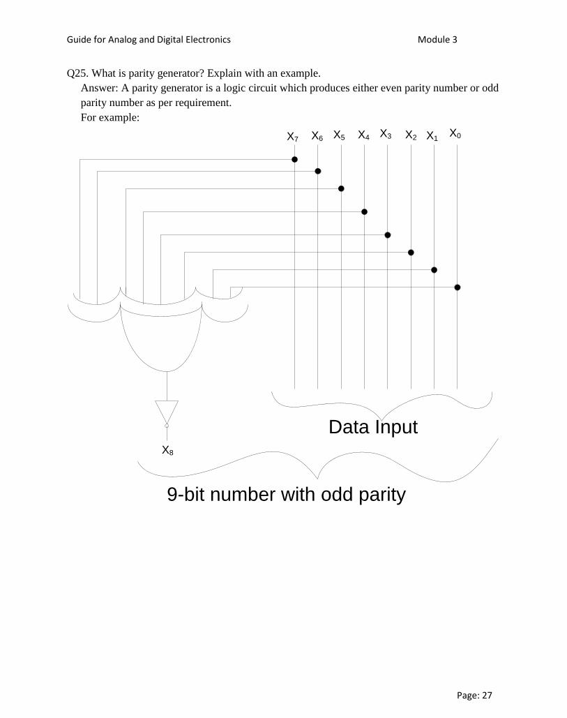
Guide for Analog and Digital Electronics Module 3
Page: 27
Q25. What is parity generator? Explain with an example.
Answer: A parity generator is a logic circuit which produces either even parity number or odd
parity number as per requirement.
For example:
X7 X6 X5 X4 X3 X2 X1X0
X8
Data Input
9-bit number with odd parity
PDF Watermark Remover DEMO : Purchase from www.PDFWatermarkRemover.com to remove the watermark
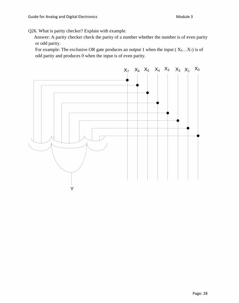
Guide for Analog and Digital Electronics Module 3
Page: 28
Q26. What is parity checker? Explain with example.
Answer: A parity checker check the parity of a number whether the number is of even parity
or odd parity.
For example: The exclusive OR gate produces an output 1 when the input ( X0…X7) is of
odd parity and produces 0 when the input is of even parity.
X7 X6 X5 X4 X3 X2 X1X0
Y
PDF Watermark Remover DEMO : Purchase from www.PDFWatermarkRemover.com to remove the watermark

Guide for Analog and Digital Electronics Module 3
Page: 29
Q27. Give state transition diagram of SR, D, JK and T flip flops.
Answer:
0 1 0 1
0 1 0 1
State Transition Diagram
SR flip flop
S R 0 0 1
0 0J K T0
0 0
0 1
1 0
0 0
0 11 0 0
D
0
1 1
1 0
0 11 1
1
1
0
11 0
0 1 D flip flop
JK flip flop
T flip flop
S R
S R
S R
J K
J K
J K
D
D
D
T
T
T
PDF Watermark Remover DEMO : Purchase from www.PDFWatermarkRemover.com to remove the watermark

Guide for Analog and Digital Electronics Module 3
Page: 30
Q28. Obtain the characteristic equation of SR, JK, D and T flip flops.
Answer:
0 1 0 1
0 1 0 1
State Transition Diagram
SR flip flop
S R 0 0 1
0 0J K T0
0 0
0 1
1 0
0 0
0 11 0 0
D
0
1 1
1 0
0 11 1
1
1
0
11 0
0 1 D flip flop
JK flip flop
T flip flop
S R
S R
S R
J K
J K
J K
D
D
D
T
T
T
Excitation Table for SR, JK, D and T flip flop is given below is prepared State Transition
Diagram above
Qn → Qn+1 S R J K D T
0 0
0 1
1 0
1 1
0 X
1 0
0 1
X 0
0 X
1 X
X 1
X 0
0
1
0
1
0
1
1
0
PDF Watermark Remover DEMO : Purchase from www.PDFWatermarkRemover.com to remove the watermark
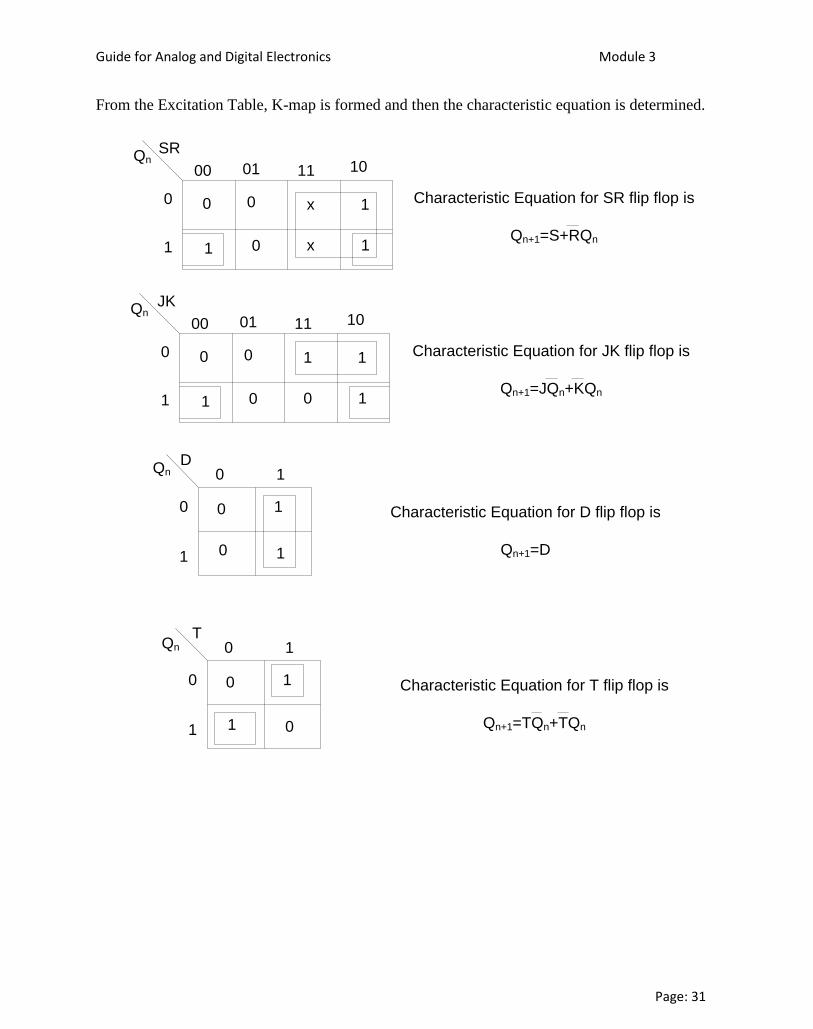
Guide for Analog and Digital Electronics Module 3
Page: 31
From the Excitation Table, K-map is formed and then the characteristic equation is determined.
SRQn
00 01 11 10
0
1
0
1
0
0
x
x
1
1
Characteristic Equation for SR flip flop is
Qn+1=S+RQn
JKQn
00 01 11 10
0
1
0
1
0
0
1
0
1
1
Characteristic Equation for JK flip flop is
Qn+1=JQn+KQn
DQn 0 1
0
1
0
0
1
1
Characteristic Equation for D flip flop is
Qn+1=D
T0 1
0
1
0
1
1
0
Characteristic Equation for T flip flop is
Qn+1=TQn+TQn
Qn
PDF Watermark Remover DEMO : Purchase from www.PDFWatermarkRemover.com to remove the watermark
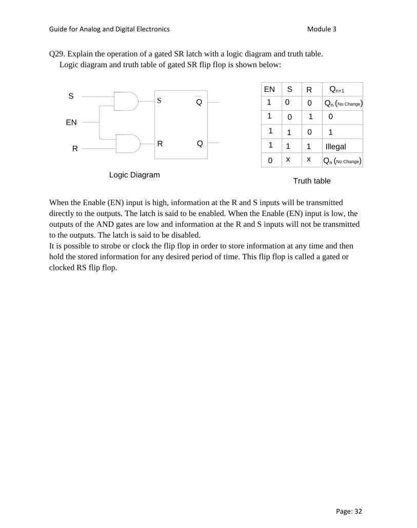
Guide for Analog and Digital Electronics Module 3
Page: 32
Q29. Explain the operation of a gated SR latch with a logic diagram and truth table.
Logic diagram and truth table of gated SR flip flop is shown below:
S
R
S
R
EN
Q
Q
EN S R Qn+1
1
1
1
1
0
0
0
1
1
x
0
1
0
1
x
Qn (No Change)
0
1
Illegal
Qn (No Change)
Logic DiagramTruth table
When the Enable (EN) input is high, information at the R and S inputs will be transmitted
directly to the outputs. The latch is said to be enabled. When the Enable (EN) input is low, the
outputs of the AND gates are low and information at the R and S inputs will not be transmitted
to the outputs. The latch is said to be disabled.
It is possible to strobe or clock the flip flop in order to store information at any time and then
hold the stored information for any desired period of time. This flip flop is called a gated or
clocked RS flip flop.
PDF Watermark Remover DEMO : Purchase from www.PDFWatermarkRemover.com to remove the watermark

Guide for Analog and Digital Electronics Module 3
Page: 33
Q30. Explain the operation of edge triggered ‘SR’ flip flop with the help of a logic diagram and
truth table. Also draw the relevant waveforms.
Answer: Positive edge triggered ‘SR’ flip flop
S
R
S
R
Q
Q
C S R Qn+1
0
0
1
1
0
1
0
1
Qn (No Change)
0 ( Reset )
1 ( Set )
Illegal
Logic Diagram
Truth table
CPT
S
C
R
Q
Q
IEEE Symbol
t0 t1 t2 t3 t4
C
PT
S
R
Q
Waveform of positive edge triggered RS flip flop
Positive edges occur at t0,t1,t2,t3 and t4.
At t0, S=0 and R=0, hence no change in the output and Q=0.
At t1, S=1 and R=0, hence the output is set and Q=1.
At t2, S=0 and R=1, hence the output is reset and Q=0.
At t3, S=1 and R=0, hence the output is set and Q=1
At t4, S=0 and R=0, hence no change in the output and Q=1.
PDF Watermark Remover DEMO : Purchase from www.PDFWatermarkRemover.com to remove the watermark

Guide for Analog and Digital Electronics Module 3
Page: 34
Negative edge triggered ‘SR’ flip flop
S
R
S
R
Q
Q
C S R Qn+1
0
0
1
1
0
1
0
1
Qn (No Change)
0 ( Reset )
1 ( Set )
Illegal
Logic Diagram
Truth table
CNT
S
C
R
Q
Q
SR flip flop Symbol
t0 t1 t2 t3 t4
C
PT
S
R
Q
Waveform of negative edge triggered SR flip flop
.
Negative edges occur at t0,t1,t2,t3 and t4.
At t0, S=0 and R=0, hence no change in the output and Q=0.
At t1, S=1 and R=0, hence the output is set and Q=1.
At t2, S=0 and R=1, hence the output is reset and Q=0.
At t3, S=1 and R=0, hence the output is set and Q=1
At t4, S=0 and R=0, hence no change in the output and Q=1.
PDF Watermark Remover DEMO : Purchase from www.PDFWatermarkRemover.com to remove the watermark

Guide for Analog and Digital Electronics Module 3
Page: 35
Q31. Explain the operation of edge triggered ‘D’ flip flop with the help of a logic diagram and
truth table. Also draw the relevant waveforms.
Answer: Positive edge triggered ‘D’ flip flop
S
R
Q
Q
C D Qn+1
x
0
1
Qn (No Change)
0
1
Logic Diagram
Truth table
CPT
D
C
Q
Q
D flip flop Symbol
t0 t1 t2 t3 t4
C
PT
D
Q
Waveform of positive edge triggered D flip flop
D
0
Positive edges occur at t0,t1,t2,t3 and t4.
At t0, D=0, hence the output is low and Q=0.
At t1, D=1, hence the output is high and Q=1.
At t2, D =0, hence the output is low and Q=0.
At t3, D=1, hence the output is high and Q=1
At t4, D=0, hence no change in the output and Q=1.
PDF Watermark Remover DEMO : Purchase from www.PDFWatermarkRemover.com to remove the watermark
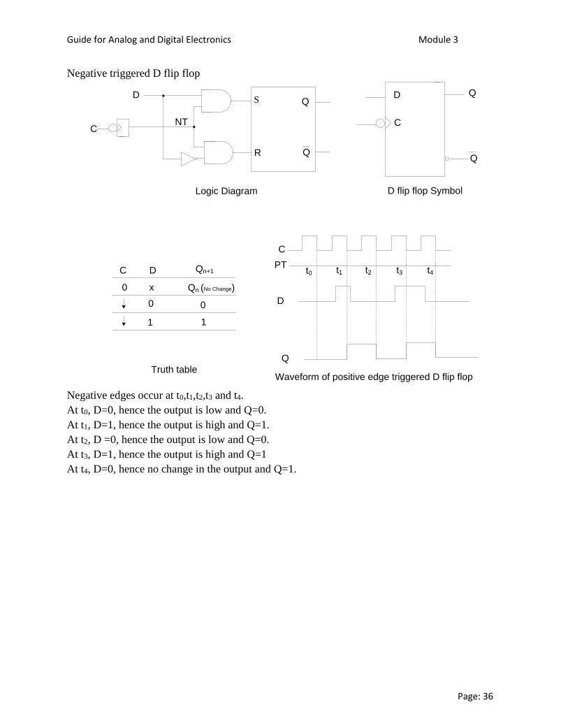
Guide for Analog and Digital Electronics Module 3
Page: 36
Negative triggered D flip flop
S
R
Q
Q
C D Qn+1
x
0
1
Qn (No Change)
0
1
Logic Diagram
Truth table
CNT
D
C
Q
Q
D flip flop Symbol
t0 t1 t2 t3 t4
C
PT
D
Q
Waveform of positive edge triggered D flip flop
D
0
Negative edges occur at t0,t1,t2,t3 and t4.
At t0, D=0, hence the output is low and Q=0.
At t1, D=1, hence the output is high and Q=1.
At t2, D =0, hence the output is low and Q=0.
At t3, D=1, hence the output is high and Q=1
At t4, D=0, hence no change in the output and Q=1.
PDF Watermark Remover DEMO : Purchase from www.PDFWatermarkRemover.com to remove the watermark

Guide for Analog and Digital Electronics Module 3
Page: 37
Q32. Explain the working of pulse triggered JK flip flop with typical JK flip flop waveform.
Answer: Positive Edge Triggered JK flip flop
S
R
J
K
Q
Q
C J K Qn+1
0
0
1
1
0
1
0
1
Qn (No Change)
0
1
Toggle
Logic Diagram
Truth table
CPT
J
C
K
Q
Q
JK flip flop Symbol
t0 t1 t2 t3 t4
C
PT
J
K
Q
Waveform of positive edge triggered JK flip flop
Positive edges occur at t0,t1,t2,t3 and t4.
At t0, J=0 and K=0, hence no change in the output and Q=0.
At t1, J=1 and K=0, hence the output is high and Q=1.
At t2, J=0 and K=1, hence the output is low and Q=0.
At t3, J=1 and K=0, hence the output is high and Q=1
At t4, J=0 and K=0, hence no change in the output and Q=1.
:
PDF Watermark Remover DEMO : Purchase from www.PDFWatermarkRemover.com to remove the watermark

Guide for Analog and Digital Electronics Module 3
Page: 38
Negative Edge Triggered JK flip flop
S
R
J
K
Q
Q
C J K Qn+1
0
0
1
1
0
1
0
1
Qn (No Change)
0
1
Toggle
Logic Diagram
Truth table
CNT
J
C
K
Q
Q
JK flip flop Symbol
t0 t1 t2 t3 t4
C
NT
J
K
Q
Waveform of positive edge triggered JK flip flop
Negative edges occur at t0,t1,t2,t3 and t4.
At t0, J=0 and K=0, hence no change in the output and Q=0.
At t1, J=1 and K=0, hence the output is high and Q=1.
At t2, J=0 and K=1, hence the output is low and Q=0.
At t3, J=1 and K=0, hence the output is high and Q=1
At t4, J=0 and K=0, hence no change in the output and Q=1.
PDF Watermark Remover DEMO : Purchase from www.PDFWatermarkRemover.com to remove the watermark
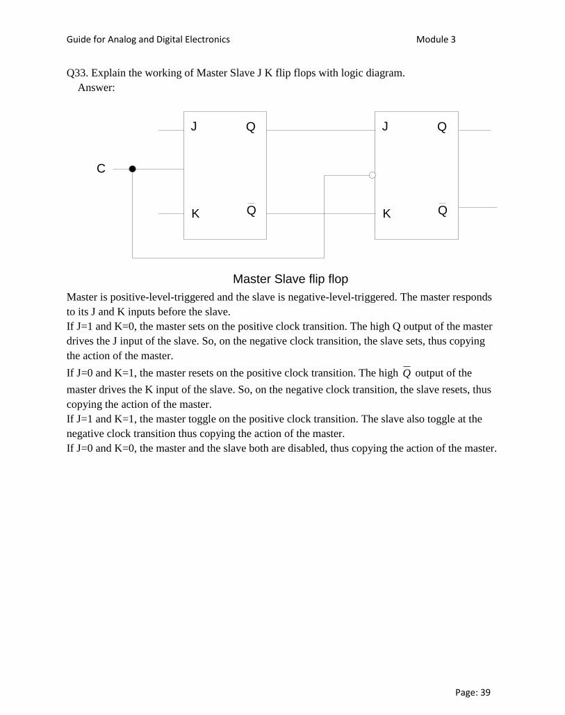
Guide for Analog and Digital Electronics Module 3
Page: 39
Q33. Explain the working of Master Slave J K flip flops with logic diagram.
Answer:
J
K
Q
Q
J
K
Q
Q
C
Master Slave flip flop
Master is positive-level-triggered and the slave is negative-level-triggered. The master responds
to its J and K inputs before the slave.
If J=1 and K=0, the master sets on the positive clock transition. The high Q output of the master
drives the J input of the slave. So, on the negative clock transition, the slave sets, thus copying
the action of the master.
If J=0 and K=1, the master resets on the positive clock transition. The high Q output of the
master drives the K input of the slave. So, on the negative clock transition, the slave resets, thus
copying the action of the master.
If J=1 and K=1, the master toggle on the positive clock transition. The slave also toggle at the
negative clock transition thus copying the action of the master.
If J=0 and K=0, the master and the slave both are disabled, thus copying the action of the master.
PDF Watermark Remover DEMO : Purchase from www.PDFWatermarkRemover.com to remove the watermark

Guide for Analog and Digital Electronics Module 3
Page: 40
Q34. What is contact bounce? With neat diagram, explain the working principles of Switch De
bounce circuit.
Answer:
5V
S
A
R
Voltage at A
5V
0V
Bounce
Any mechanical switching device consists of a moving contact arm restrained by some spring
system. As a result, when a mechanical switch is closed, the arm is moved from one stable
position to other and the arm bounces much as a hard ball bounces when dropped on a hard
surface. This phenomenon is known as contact bounce. When switch S is closed, due contact
bounce the voltage at the A is shown in the above figure.
RS Latch Debounce Circuit
+VCC
SW
H
L
R1
R2
S
R
Q
When switch(SW) is moved to the position H, R=0 and S=1. Bouncing occurs at S due to contact
bounce of the switch. The flip flop treat as high and low inputs. The flip flop will be set with
Q=1 at the firs high of the contact bounce. When the switch continue to bounce, losing contact,
the input signals are R=S=0, thus the flip flop remains at Q=1. As a result, the flip flop responds
only to the first high of the contact bounce.
PDF Watermark Remover DEMO : Purchase from www.PDFWatermarkRemover.com to remove the watermark

Guide for Analog and Digital Electronics Module 4
Page: 1
Q1. Explain 4-bit Serial in-Serial out register.
Answer: 4-bit serial in-serial out register is shown below:
D Q
Q
D R
R
D S
S
D T
T
Serial Data
Input
Clock
The waveform for the above circuit is shown below:
It has been assumed that initially Q=0, R=0, S=0 and T=0.
TimeA B C D
Clock1
0
1
0
1
0
1
0
1
0
1
0
Q
R
S
T
D
1
0
1
0
At clock edge A: DQRS=0000. As the clock trigger at A, the values at DQRS is transferred to
QRST and QRST=0000.

Guide for Analog and Digital Electronics Module 4
Page: 2
At clock edge B: DQRS=1000. As the clock trigger at B, the values at DQRS is transferred to
QRST and QRST=1000.
At clock edge C: DQRS=0100. As the clock trigger at C, the values at DQRS is transferred to
QRST and QRST=0100.
At clock edge D: DQRS=1010. As the clock trigger at B, the values at DQRS is transferred to
QRST and QRST=1010.
Q2. Explain 4-bit Serial in-parallel out register.
Answer: 4-bit serial in-parallel out register is shown below:
R
S
QA
QA
R
S
QB
QB
R
S
QC
QC
R
S
QD
QD
Serial Data
Input
QA QB QC QD
AB
Clock
Parallel data output
Data shifted in serially, but shifted out in parallel as shown in the figure above. In order to shift
the data out in parallel, output of each flip flop is connected to output pin.
Suppose that the serial data is connected to A, and then B can be used as a control line.
If B is held high, then the NAND gate is enabled and the serial input data passes through the
NAND gate is inverted. The input data is shifted serially into the register.
If B is held low, then the NAND gate output is high irrespective of input data.
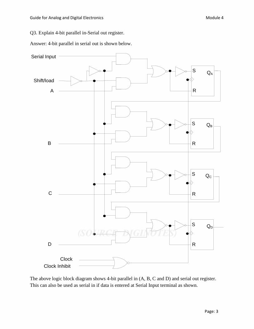
Guide for Analog and Digital Electronics Module 4
Page: 3
Q3. Explain 4-bit parallel in-Serial out register.
Answer: 4-bit parallel in serial out is shown below.
Serial Input
Shift/load
S
R
S
R
S
R
S
R
QA
QB
QC
QD
Clock
Clock Inhibit
A
B
C
D
The above logic block diagram shows 4-bit parallel in (A, B, C and D) and serial out register.
This can also be used as serial in if data is entered at Serial Input terminal as shown.
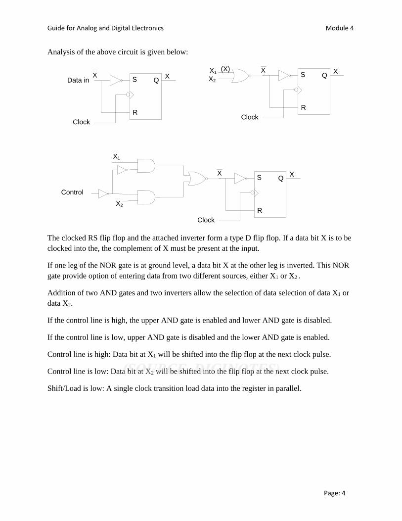
Guide for Analog and Digital Electronics Module 4
Page: 4
Analysis of the above circuit is given below:
Data in
Clock
X XQS
RClock
X XQS
R
X1
X2
(X)
Clock
X XQS
R
X1
X2
Control
The clocked RS flip flop and the attached inverter form a type D flip flop. If a data bit X is to be
clocked into the, the complement of X must be present at the input.
If one leg of the NOR gate is at ground level, a data bit X at the other leg is inverted. This NOR
gate provide option of entering data from two different sources, either X1 or X2 .
Addition of two AND gates and two inverters allow the selection of data selection of data X1 or
data X2.
If the control line is high, the upper AND gate is enabled and lower AND gate is disabled.
If the control line is low, upper AND gate is disabled and the lower AND gate is enabled.
Control line is high: Data bit at X1 will be shifted into the flip flop at the next clock pulse.
Control line is low: Data bit at X2 will be shifted into the flip flop at the next clock pulse.
Shift/Load is low: A single clock transition load data into the register in parallel.

Guide for Analog and Digital Electronics Module 4
Page: 5
Q4. Explain 4-bit parallel in-parallel out register.
Answer: 4-bit parallel in parallel out is shown below.
D
D
Q
Q
Q
Q
D
D
QA
QB
QC
QD
D1
D2
D3
D4
Clock
Parallel
Input
Parallel
Output
Data D1 through D4 are shifted into the register with clock pulse. The stored data is immediately
available in parallel at the output Q1 through Q4. This type of register is used to store data is
called data latch or data register..
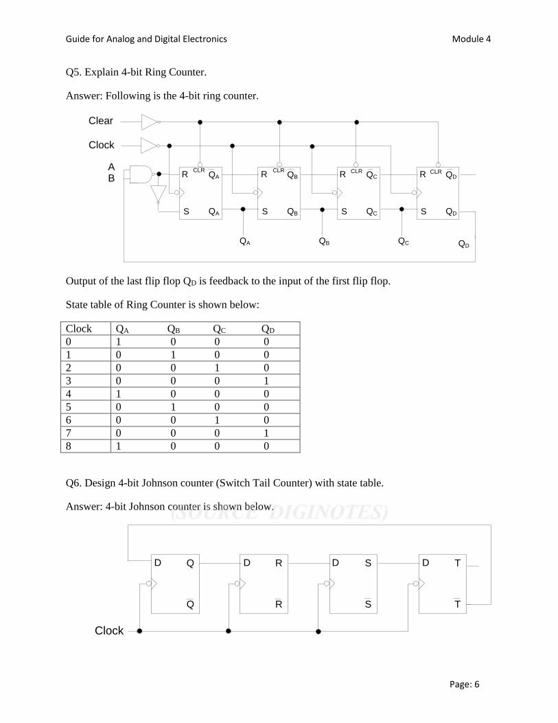
Guide for Analog and Digital Electronics Module 4
Page: 6
Q5. Explain 4-bit Ring Counter.
Answer: Following is the 4-bit ring counter.
R
S
QA
QA
R
S
QB
QB
R
S
QC
QC
R
S
QD
QD
QA QB QC QD
AB
Clock
CLRCLRCLRCLR
Clear
Output of the last flip flop QD is feedback to the input of the first flip flop.
State table of Ring Counter is shown below:
Clock QA QB QC QD
0 1 0 0 0
1 0 1 0 0
2 0 0 1 0
3 0 0 0 1
4 1 0 0 0
5 0 1 0 0
6 0 0 1 0
7 0 0 0 1
8 1 0 0 0
Q6. Design 4-bit Johnson counter (Switch Tail Counter) with state table.
Answer: 4-bit Johnson counter is shown below.
D Q
Q
D R
R
D S
S
D T
T
Clock
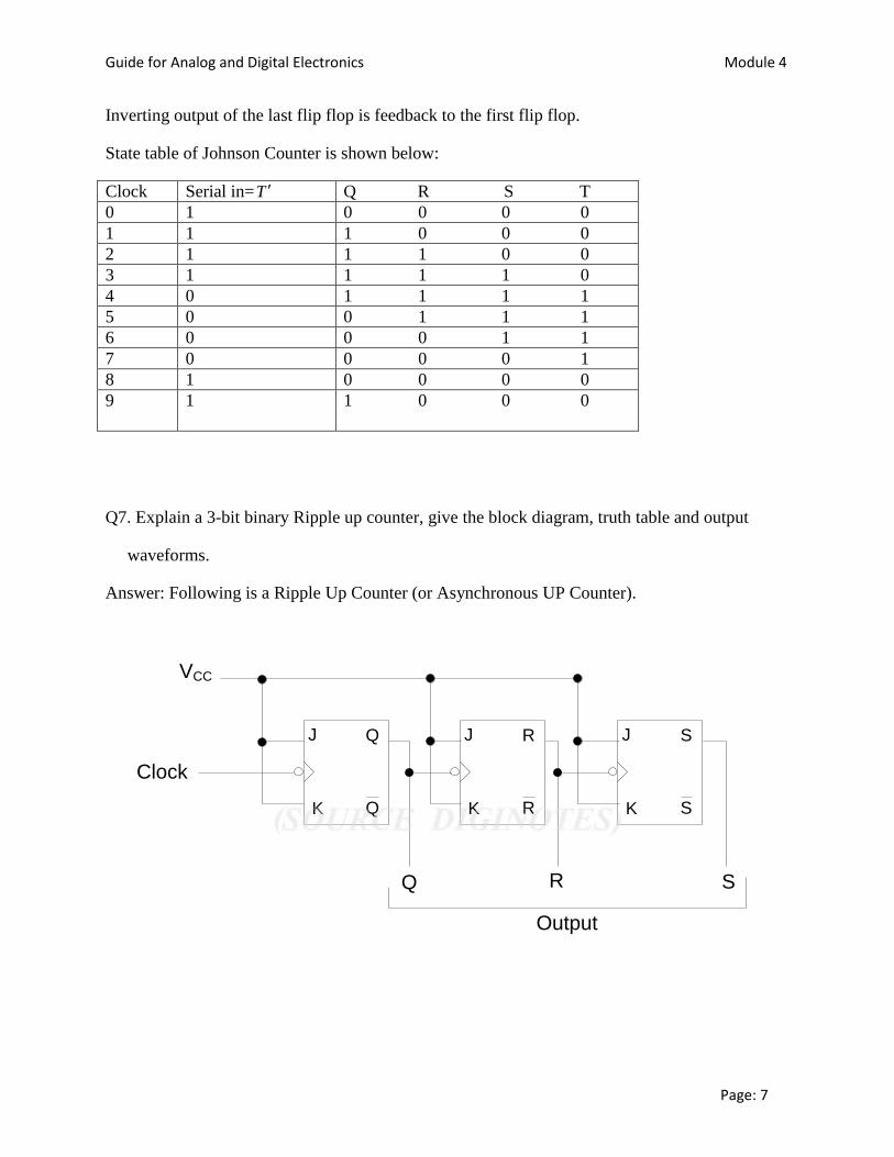
Guide for Analog and Digital Electronics Module 4
Page: 7
Inverting output of the last flip flop is feedback to the first flip flop.
State table of Johnson Counter is shown below:
Clock Serial in=T Q R S T
0 1 0 0 0 0
1 1 1 0 0 0
2 1 1 1 0 0
3 1 1 1 1 0
4 0 1 1 1 1
5 0 0 1 1 1
6 0 0 0 1 1
7 0 0 0 0 1
8 1 0 0 0 0
9
1 1 0 0 0
Q7. Explain a 3-bit binary Ripple up counter, give the block diagram, truth table and output
waveforms.
Answer: Following is a Ripple Up Counter (or Asynchronous UP Counter).
J
K
Q
Q
J
K
R
R
J
K
S
S
Clock
VCC
Q R S
Output
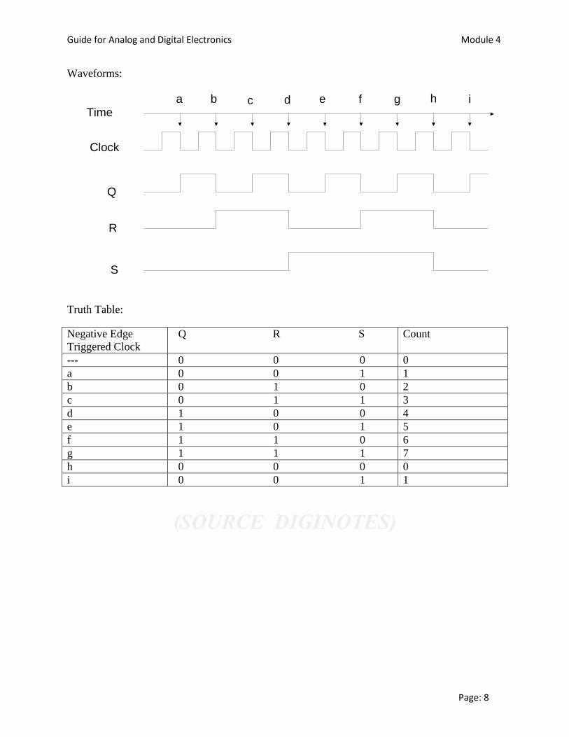
Guide for Analog and Digital Electronics Module 4
Page: 8
Waveforms:
Time
Clock
Q
R
S
a b c d e f g h i
Truth Table:
Negative Edge
Triggered Clock
Q R S Count
--- 0 0 0 0
a 0 0 1 1
b 0 1 0 2
c 0 1 1 3
d 1 0 0 4
e 1 0 1 5
f 1 1 0 6
g 1 1 1 7
h 0 0 0 0
i 0 0 1 1

Guide for Analog and Digital Electronics Module 4
Page: 9
Q8. Explain a 3-bit binary Ripple down counter, give the block diagram, truth table and output
waveforms.
Answer: Following is a Ripple Down Counter (or Asynchronous Down Counter).
J
K
Q
Q
J
K
R
R
J
K
S
S
Clock
VCC
Q R S
Output
Waveforms:
Time
Clock
Q
R
S
a b c d e f g h i

Guide for Analog and Digital Electronics Module 4
Page: 10
Truth Table:
Negative Edge
Triggered Clock
Q R S Count
--- 0 0 0 0
a 1 1 1 7
b 1 1 0 6
c 1 0 1 5
d 1 0 0 4
e 0 1 1 3
f 0 1 0 2
g 0 0 1 1
h 0 0 0 0
i 1 1 1 7
Q9. Explain a 3-bit Ripple Up Down Counter.
Answer: Following is a Ripple Up Down Counter.
J
K
Q
Q
J
K
R
R
J
K
S
S
Clock
VCC
Q R S
Count Up
Count Down
Ripple Up Down Counter is combination Ripple Up Counter and Ripple Down Counter.
If Count Up control is high and Count Down control is low, the above counter will be Up
Counter.
If Count Up control is low and Count Down control is high, the above counter will be Down
Counter.

Guide for Analog and Digital Electronics Module 4
Page: 11
Q10. Explain the 7493 IC.
Answer: Following is the 7493 IC
J
J
Q
Q
Q
Q
J
J
QA
QB
QC
QD
K
K
K
K
CLK A
CLK B
R0(1)
R0(2)
7493 IC is a 4 bit binary counter that can be used in either mod-8 or mod-16.
If the clock is applied at CLK B, the counter will be mod-8 counter and the output appear at
QB, QC and QD.
If the clock is applied at CLK A and QA is connected to CLK B, the counter will be mod-16
Counter and the output appear at QA, QB, QC and QD.
R0(1) and R0(2) are used to reset all flip flops simultaneously.
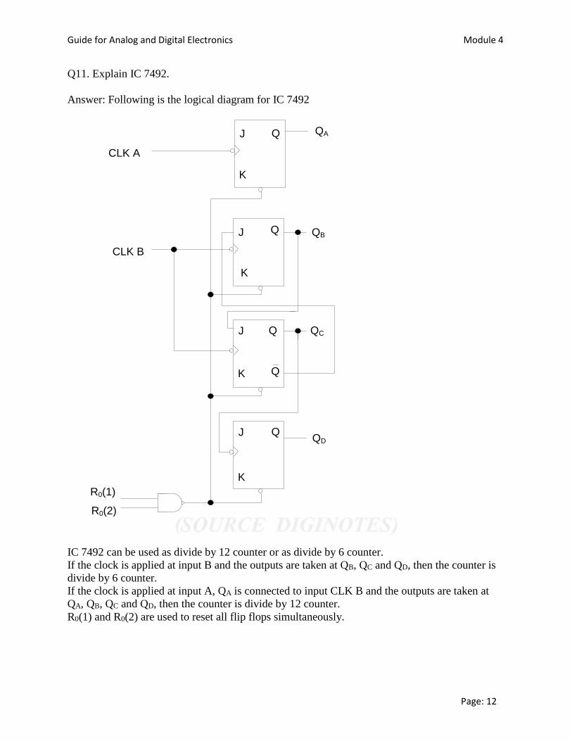
Guide for Analog and Digital Electronics Module 4
Page: 12
Q11. Explain IC 7492.
Answer: Following is the logical diagram for IC 7492
J
J
Q
Q
Q
Q
J
J
QA
QB
QC
QD
K
K
K
K
CLK A
CLK B
R0(1)
R0(2)
Q
IC 7492 can be used as divide by 12 counter or as divide by 6 counter.
If the clock is applied at input B and the outputs are taken at QB, QC and QD, then the counter is
divide by 6 counter.
If the clock is applied at input A, QA is connected to input CLK B and the outputs are taken at
QA, QB, QC and QD, then the counter is divide by 12 counter.
R0(1) and R0(2) are used to reset all flip flops simultaneously.
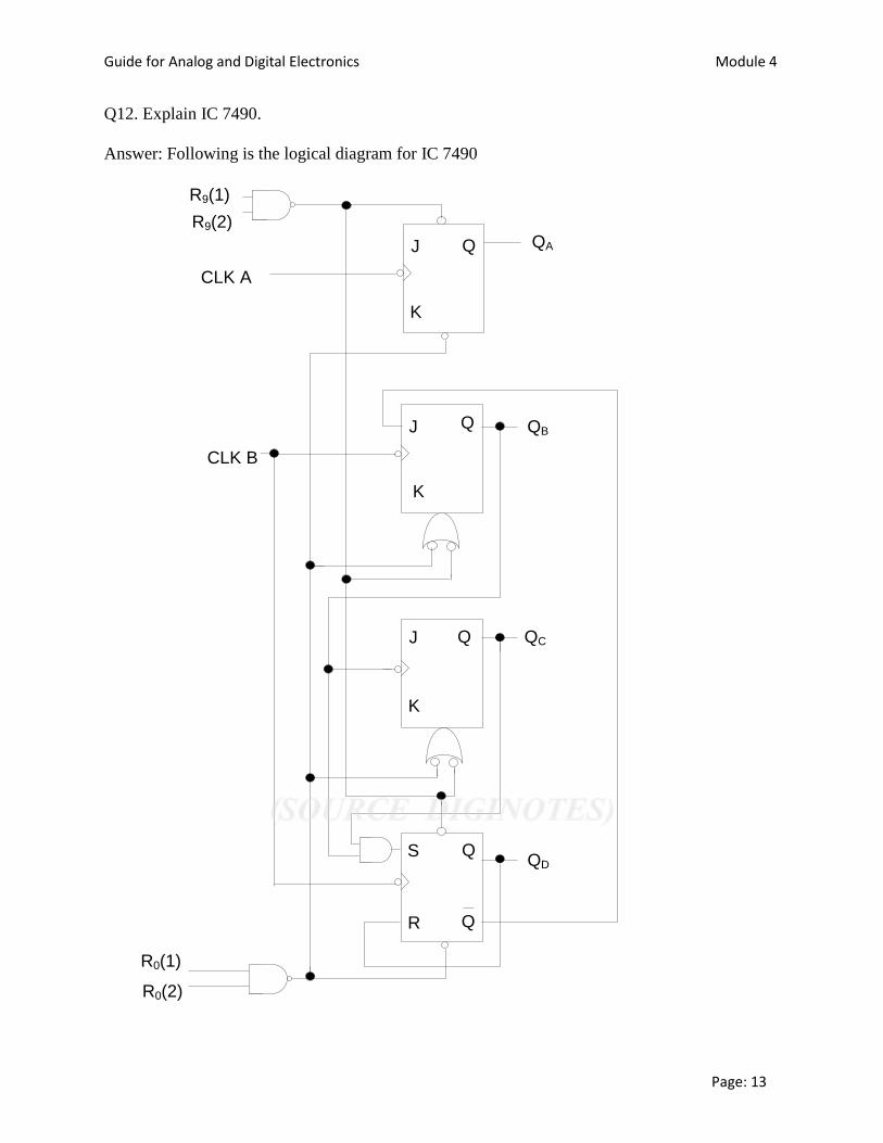
Guide for Analog and Digital Electronics Module 4
Page: 13
Q12. Explain IC 7490.
Answer: Following is the logical diagram for IC 7490
J
J
Q
Q
Q
Q
J
S
QA
QB
QC
QD
K
K
R
K
CLK A
CLK B
R0(1)
R0(2)
Q
R9(1)
R9(2)

Guide for Analog and Digital Electronics Module 4
Page: 14
IC 7490 is a decade counter. If the system clock is applied at CLK A and QA is connected to
CLK B, then the counter is a decade counter.
R0(1) and R0(2) are used to reset all flip flops simultaneously.
Q13. Design divide by 9 counter using IC 7492.
Answer: Following is the logic diagram to implement divide by 9 counter using IC 7492.
R(1) R(2)
QA QB QC QD
IC7492CLK A
CLK B
IC 7492 is a mod-12 counter when QA is connected to CLK B.
In the above diagram, when QDQCQBQA=1001, output of the AND gate is high and as a result,
the counter reset as QDQCQBQA=0000. Thus, the above circuit is a divide by 9 counter.
Q14. Design a divide by 128 counter using 7493 ICs.
Answer: Following is the logic diagram divide by 128 counter.
128=16x8. First IC 7493 is used as divide by 16. The CLK B is input from QA and the external
clock is applied at CLK A.
Second IC 7493 is used as divide by 8. CLK A is unused. CLK B is input from QD of the first IC.
R(1) R(2)
QA QB QC QD
IC7493CLK A
CLK B
R(1) R(2)
QA QB QC QD
IC7493CLK A
CLK B
Q0 Q1 Q2 Q3 Q4 Q5 Q6

Guide for Analog and Digital Electronics Module 4
Page: 15
Q15. Design a divide by 78 counter using 7493 and 7492 counter ICs.
Answer: Following is the logic diagram divide by 78 counter.
R(1) R(2)
QA QB QC QD
IC7492CLK A
CLK B
R(1) R(2)
QA QB QC QD
IC7493CLK A
CLK B
Q0 Q1 Q2 Q3 Q4 Q5 Q6
78=6x13.
IC 7492 is used as divide by 6 counter.CLK A is unused and the external clock is applied to the
CLK B.
IC 7493 is to be used as divide by 13 counter. To make this as divide by 13 counter, QD of IC
7492 is connected to the CLK A of IC 7493. QA, QC and QD are connected as input to a AND
gate and output of the AND gate is connected reset pins.
Q16. Design mod-3 synchronous counter.
Answer:
Truth Table
Clock Counter Output
Q2 Q1
0 0 0
1 0 1
2 1 0
3 0 0
J K Qn+1
Action
No Change
Reset
Set
Toggle
Qn
0
1
Qn
0 0
0 1
1 0
1 1
0 1
J K
0 00 1
0 X
J K
1 01 1
1 X
J K
0 0
1 0
X 0
0 11 1
X 1
J K
Truth Table for JK Flip Flop
State Transition Diagram for JK Flip Flop
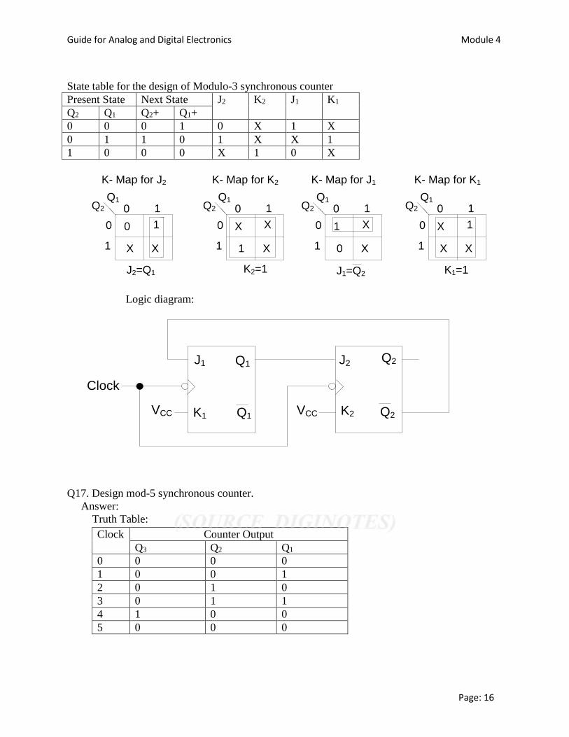
Guide for Analog and Digital Electronics Module 4
Page: 16
State table for the design of Modulo-3 synchronous counter
Present State Next State J2 K2 J1 K1
Q2 Q1 Q2+ Q1+
0 0 0 1 0 X 1 X
0 1 1 0 1 X X 1
1 0 0 0 X 1 0 X
K- Map for J2
0 1
0
1
Q2
Q1
0 1
X X
K- Map for K2
0 1
0
1
Q2
Q1
X X
1 X
K- Map for J1
0 1
0
1
Q2
Q1
1 X
0 X
K- Map for K1
0 1
0
1
Q2
Q1
X 1
X X
J2=Q1 K2=1 J1=Q2 K1=1
Logic diagram:
J1
K1
J2
K2
Q1
Q1
Q2
Q2VCC
Clock
VCC
Q17. Design mod-5 synchronous counter.
Answer:
Truth Table:
Clock Counter Output
Q3 Q2 Q1
0 0 0 0
1 0 0 1
2 0 1 0
3 0 1 1
4 1 0 0
5 0 0 0
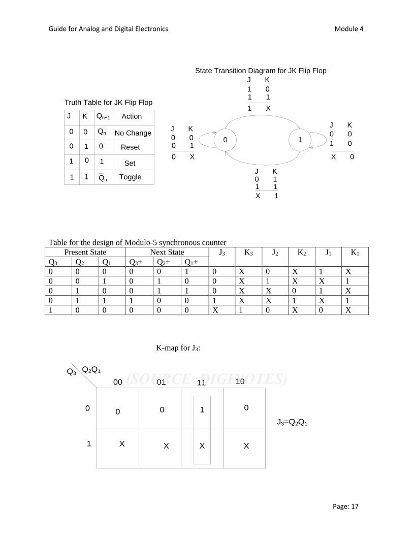
Guide for Analog and Digital Electronics Module 4
Page: 17
J K Qn+1
Action
No Change
Reset
Set
Toggle
Qn
0
1
Qn
0 0
0 1
1 0
1 1
0 1
J K
0 00 1
0 X
J K
1 01 1
1 X
J K
0 0
1 0
X 0
0 11 1
X 1
J K
Truth Table for JK Flip Flop
State Transition Diagram for JK Flip Flop
Table for the design of Modulo-5 synchronous counter
Present State Next State J3 K3 J2 K2 J1 K1
Q3 Q2 Q1 Q3+ Q2+ Q1+
0 0 0 0 0 1 0 X 0 X 1 X
0 0 1 0 1 0 0 X 1 X X 1
0 1 0 0 1 1 0 X X 0 1 X
0 1 1 1 0 0 1 X X 1 X 1
1 0 0 0 0 0 X 1 0 X 0 X
K-map for J3:
Q2Q1Q3
00 01 11 10
0
1
0
J3=Q2Q1
0 0
X
1
XX X
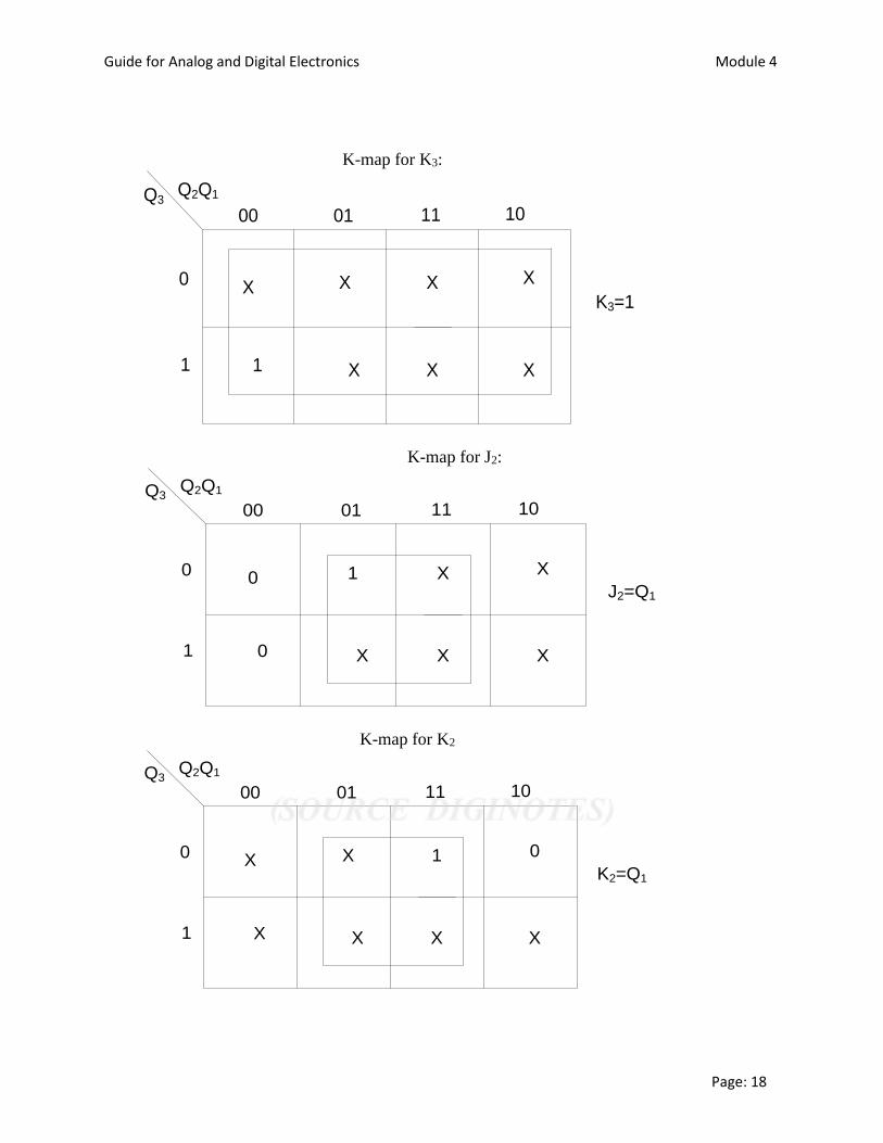
Guide for Analog and Digital Electronics Module 4
Page: 18
K-map for K3:
Q2Q1Q3
00 01 11 10
0
1
XK3=1
X X
1
X
XX X
K-map for J2:
Q2Q1Q3
00 01 11 10
0
1
0J2=Q1
1 X
0
X
XX X
K-map for K2
Q2Q1Q3
00 01 11 10
0
1
XK2=Q1
X 0
X
1
XX X

Guide for Analog and Digital Electronics Module 4
Page: 19
K-map for J1:
Q2Q1Q3
00 01 11 10
0
1
1
J1=Q3
X 1
0
X
XX X
K-map for K1:
Q2Q1Q3
00 01 11 10
0
1
XK1=1
1 X
1
1
XX X
Logic Diagram:
J1
K1
J2
K2
J3
K3
Q1
Q1
Q2
Q2
Q3
Q3VCC VCC
Clock
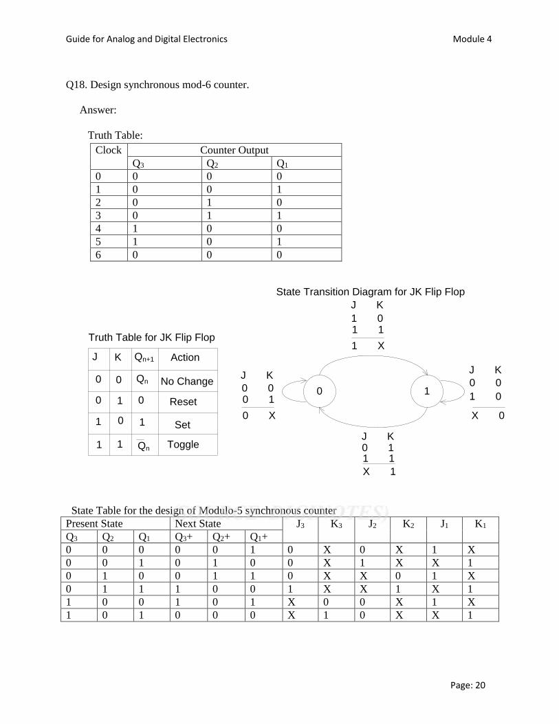
Guide for Analog and Digital Electronics Module 4
Page: 20
Q18. Design synchronous mod-6 counter.
Answer:
Truth Table:
Clock Counter Output
Q3 Q2 Q1
0 0 0 0
1 0 0 1
2 0 1 0
3 0 1 1
4 1 0 0
5 1 0 1
6 0 0 0
J K Qn+1
Action
No Change
Reset
Set
Toggle
Qn
0
1
Qn
0 0
0 1
1 0
1 1
0 1
J K
0 00 1
0 X
J K
1 01 1
1 X
J K
0 0
1 0
X 0
0 11 1
X 1
J K
Truth Table for JK Flip Flop
State Transition Diagram for JK Flip Flop
State Table for the design of Modulo-5 synchronous counter
Present State Next State J3 K3 J2 K2 J1 K1
Q3 Q2 Q1 Q3+ Q2+ Q1+
0 0 0 0 0 1 0 X 0 X 1 X
0 0 1 0 1 0 0 X 1 X X 1
0 1 0 0 1 1 0 X X 0 1 X
0 1 1 1 0 0 1 X X 1 X 1
1 0 0 1 0 1 X 0 0 X 1 X
1 0 1 0 0 0 X 1 0 X X 1

Guide for Analog and Digital Electronics Module 4
Page: 21
K-map for J3:
Q2Q1Q3
00 01 11 10
0
1
0
J3=Q2Q1
0 0
X
1
XX X
K-map for K3:
Q2Q1Q3
00 01 11 10
0
1
XK3=Q1
X X
0
X
X1 X
K-map for J2:
Q2Q1Q3
00 01 11 10
0
1
0J2=Q3Q1
1 X
0
X
X0 X

Guide for Analog and Digital Electronics Module 4
Page: 22
K-map for K2:
Q2Q1Q3
00 01 11 10
0
1
XK2=Q1
X 0
X
1
XX X
K-map for J1:
Q2Q1Q3
00 01 11 10
0
1
1
J1=1
X 1
1
X
XX X
K-map for K1:
Q2Q1Q3
00 01 11 10
0
1
XK1=1
1 X
1
1
XX X
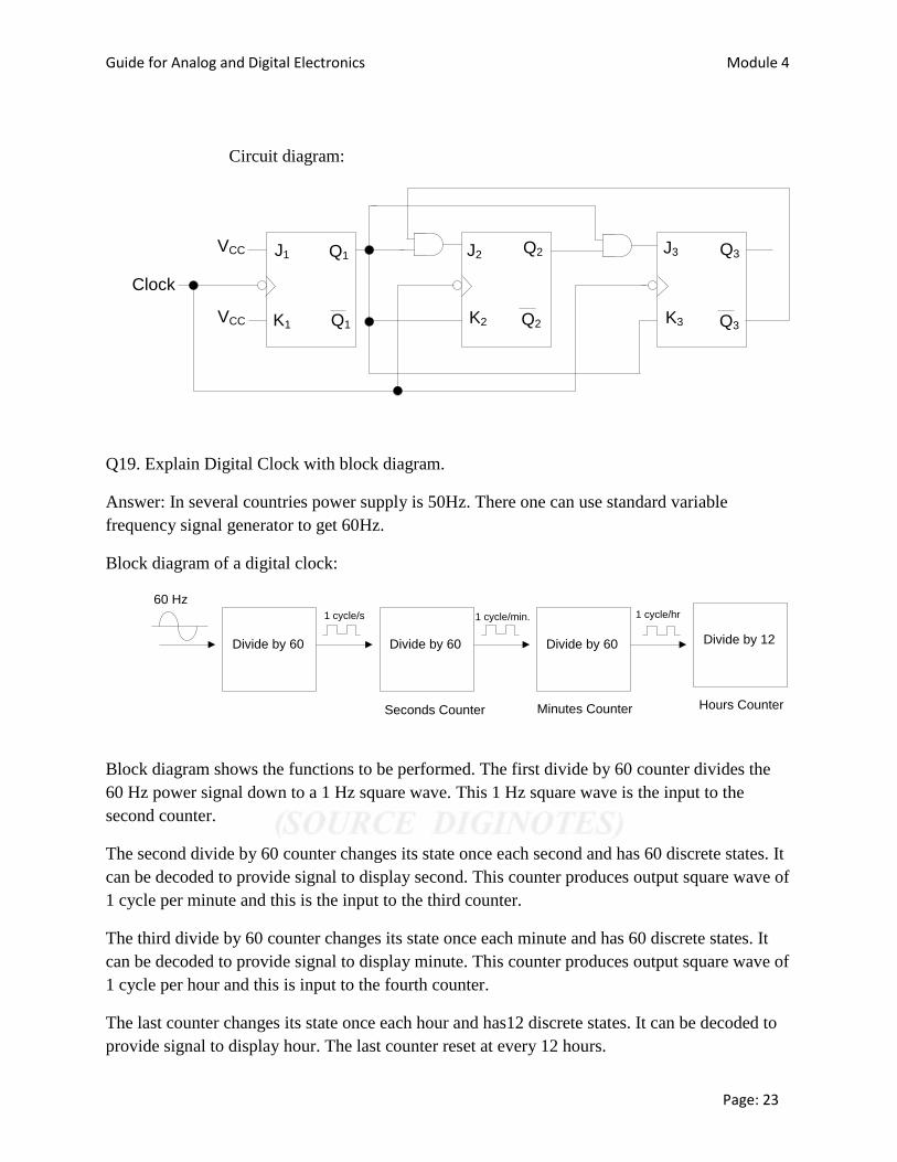
Guide for Analog and Digital Electronics Module 4
Page: 23
Circuit diagram:
J1
K1
J2
K2
J3
K3
Q1
Q1
Q2
Q2
Q3
Q3VCC
VCC
Clock
Q19. Explain Digital Clock with block diagram.
Answer: In several countries power supply is 50Hz. There one can use standard variable
frequency signal generator to get 60Hz.
Block diagram of a digital clock:
Divide by 60 Divide by 60 Divide by 60 Divide by 12
60 Hz
1 cycle/s 1 cycle/min. 1 cycle/hr
Seconds Counter Minutes Counter Hours Counter
Block diagram shows the functions to be performed. The first divide by 60 counter divides the
60 Hz power signal down to a 1 Hz square wave. This 1 Hz square wave is the input to the
second counter.
The second divide by 60 counter changes its state once each second and has 60 discrete states. It
can be decoded to provide signal to display second. This counter produces output square wave of
1 cycle per minute and this is the input to the third counter.
The third divide by 60 counter changes its state once each minute and has 60 discrete states. It
can be decoded to provide signal to display minute. This counter produces output square wave of
1 cycle per hour and this is input to the fourth counter.
The last counter changes its state once each hour and has12 discrete states. It can be decoded to
provide signal to display hour. The last counter reset at every 12 hours.

Guide for Analog and Digital Electronics Module 4
Page: 24
Divide by 60 counter can be implemented by cascading divide by 10 counter ( IC 7490) and
divide by 6 counter ( IC 7492). This is in the block diagram below.
60 Hz
Amplifier Divide by 10
IC 7490
Divide by 6
IC 7492
6 Hz 1 Hz
.Display of Second, Minute and Hour can be implemented by the IC 7447 and 7 segment display.
This is shown below in the following diagram.
QD QC QB QA
7492
LED
7447
QD QC QB QA
7490
LED
7447
Tens Units
Guide for Analog and Digital Electronics Module 5
Page: 1
Q1. Explain 5-bit resistive divider with diagram.
Answer: 5-bit resistive divider is shown below:
R0 R1 R2 R3 R4
=R0/2 =R0/4 =R0/8 =R0/16
(Analog Output)
V0 V1 V2 V3 V4
VA A resistive divider can be build to change a digital voltage to an equivalent analog voltage.
The following criterion can be applied to resistive divider.
There must be one input resistor for each digital bit.
Beginning with the LSB, each following resistor value is one half of the previous
resistor.
The LSB has weight of1
2 1n , where n is the number of input bits.
The change in output voltage due to a change in the LSB is equal to 22 1
V
where V is
the digital input voltage.
The output voltage can be obtained for any digital input signal by following equation. 0 1 2 3 1
0 1 2 3 12 2 2 2 ....... 2
2 1
n
nA n
V V V V VV
, where 0 1 2 1, , ,......, nV V V V are the digital
voltage (0 or V) and n is the number of input bits.
Q2. For a 5-bit resistive divider, determine the following (a) the weight assigned to the LSB
(b) the weight assigned to the second and the third LSB (c) the change in output voltage
due to a change in the LSB, the second LSB, and the third LSB (d) the output voltage for
a digital input 10101. Assume 0= 0 V and 1=+10 V.
Answer:
(a) The LSB weight is 5
1 1
2 1 31
(b) The second LSB weight is 2
31 and third LSB weight is
4
31

Guide for Analog and Digital Electronics Module 5
Page: 2
(c) The LSB causes a change in the output voltage of 10
31 V. The second LSB causes an output
voltage change of 20
31V and third LSB causes an output voltage change of
40
31 V.
(d) The output voltage for a digital input of 10101 is
0 1 2 3 4
5
10 2 0 2 10 2 0 2 10 2 10(1 4 16) 2106.77
2 1 31 31AV
V
Q3. Explain binary ladder with diagram.
Answer: Binary ladder is shown below.
RR2R
2R 2R 2R-
+
VA
+15V
-15V
B0Bn-1 Bn
Bn , Bn-1 , ….,B0 are the digital inputs, whose values are either 0 (0 Volt) or 1(V Volt).
Bn is MSB and B0 is the LSB.
1 0
1 1 1( ....... )
2 4 2A n n n
V V B B B
Q4. Find the output voltage from a 5-bit ladder that has a digital input of 11010. Assume that
0=0 V and 1=+10 V.
Answer:
1 1 1 1 1 1 1 110(1 1 0 1 0 ) 10( ) 8.125
2 4 8 16 32 2 4 16AV V

Guide for Analog and Digital Electronics Module 5
Page: 3
Q5. Explain the terms accuracy and resolution for D/A converter.
Answer:
Accuracy is a measure of how close the actual output voltage is to the theoretical output value.
For example, suppose the theoretical output voltage for a particular input is +10 V.
For accuracy of 1 percent, the actual output voltage must lies between +9.9 V and +10.1 V.
Resolution defines the smallest increment in voltage that can be recognized. Resolution is a
function of number of bits in the digital input signal. In a 4-bit ladder system, the LSB weight
of 1/16. This means that the smallest increment in output voltage is 1/16 of the input voltage.
If the input voltage is +16 V, then the output voltage changes in steps of 1 V. This converter
cannot resolve voltages smaller than 1 V. This converter is not capable of distinguishing voltages
finer than 1 V which is the resolution of the converter.
Q6. What is the resolution of a 9-bit D/A converter which uses a ladder network? What is the
resolution expressed as a percentage? If the full scale output voltage of this converter is +5 V,
What is the resolution in volts?
Answer:
In a 9-bit system, the LSB has a weight of 9
1 1
2 512 .
Hence, the resolution of the converter expressed in percentage= 1
100% 0.2%512
The resolution in volt=1
5 10512
mV
Q7. How many bits are required at the input of a converter if it is necessary to resolve voltage to
5 mV and the ladder has +10 V full scale?
Answer:
Resolution=1
full scale voltage2n
where n is the number of bits
3 15 10 10
2
2 2000
11
n
n
n

Guide for Analog and Digital Electronics Module 5
Page: 4
Q8. Explain simultaneous A/D converter with diagram.
Answer: Following is the logical diagram for 2-bit simultaneous A/D converter.
Comparator
Comparator
Comparator
C1
C2
C3
+3V/4
+V/2
+V/4
Reference
Voltage
Reference
Voltage
Reference
Voltage
Analog Input
Voltage
( 0 to V Votts)
Comparator Output
Following table shows the comparator output for input voltage ranges
Input Voltage Comparator Output
C3 C2 C1
0 to +V/4 Low Low Low
+V/4 to +V/2 Low Low High
+V/2 to +3V/4 Low High High
+3V/4 to V High High High
The simultaneous method of A/D conversion using three comparators is shown in the above
figure. The analog signal to be digitized serves as one of the inputs to each comparator. The
second input is a standard reference voltage. The reference voltages used are +V/4, +V/2 and
+3V/4. The system is then capable of accepting an analog input voltage between 0 and +V.
If the analog signal exceeds the reference voltage to any comparator, that comparator
turns on. Now, if all the comparator are off, the analog input signal must be between 0 and
+V/4. If C1 is high and C2 and C3 are low, the input must be between +V/4 and +V/2. If C1
and C2 are high and C3 is low, the input must be between +V/2 and +3V/4. If all the
comparator outputs are high, the input signal must be between +3V/4 and +V.

Guide for Analog and Digital Electronics Module 5
Page: 5
Q9. Explain counter type A/D converter with diagram.
Answer: Following is the counter type A/D converter
ClockGate and
Control
Start
Comparator
Analog
Input
Voltage
Counter
Level Amplifier
Binary Ladder
N lines
N lines
N lines
Reference
Voltage
This type of A/D converter consists of binary counter. The digital output signal of this counter
is connected to a standard binary ladder D/A converter. If a clock is applied to the input of the
counter, the output of the binary ladder D/A converter is the staircase waveform. This waveform
is the reference voltage signal for the comparator.
First, the counter is reset to all 0s. Then, when a convert signal appears on the START line,
the gate opens and the clock pulses are allowed to pass through to the input of the counter.
The counter advances through a normal binary count sequence, and the staircase waveform is
generated at the output of the ladder. This waveform is applied to one side of the comparator and
analog input voltage is applied to the other side. When the reference voltage equals (or exceeds)
the input analog voltage, the gate is closed, the counter stops and the conversion is complete. The
number stored in the counter is now the digital equivalent of the analog input voltage.

Guide for Analog and Digital Electronics Module 5
Page: 6
Q10. Explain continuous A/D converter with diagram.
Answer: Following is the continuous A/D converter:
Down
Clock
OS
S
R
S
R
UP/Down
Counter
Level
Amplifier
Ladder
N line
N line
N line
Q
Q
Q
Q Down
Advance
Count up
Count Down
Digital
output
Up
Up
Comparator
Down
Up Analog
Input
This type of A/D converter consists of binary up/down counter. The digital output signal of this
counter is connected to a standard binary ladder to form a D/A converter. Output of the ladder is
fed into a comparator which has two outputs. When the input analog voltage is more positive
than the ladder output, Up output of the comparator is high. When the input analog voltage is
more negative than the ladder output, the down output is high.
Guide for Analog and Digital Electronics Module 5
Page: 7
If the Up output of the comparator is high, the AND gate at the input of the Up flipflop open,
and the first time the clock goes positive, the flipflop is set. At moment down flipflop is reset, the
AND gate which controls the count-up line of the counter will be true and the counter advance
one count. As long as the Up line out of the comparator is high, the converter continues to
operate and advances its count.
At the point where the ladder voltage becomes more positive than the input voltage, the Up line
of the comparator goes low and the Down line goes high. The converter then goes through a
count-down conversion cycle.
Q11. Explain successive approximation converter with diagram.
Answer: Following shows the block diagram for successive approximation converter.
Contrl logic
and clock
Ring Counter
Counter
Level Amplifier
Ladder
Comp.
Digital Output
N lines
N lines
N lines
N lines
Vx
(Analog Input)

Guide for Analog and Digital Electronics Module 5
Page: 8
Following shows the operation performed in successive approximation converter
1000
1100
0100
1110
0010
1111
0001
1101
1011
1001
1010
0110
0111
0101
0011
1111
1110
1101
1100
1011
1010
1001
1000
0111
0110
0101
0100
0011
0010
0001
0000
0000
Start
Successive approximation converter consists of counter which is first reset to all 0s. The MSB of
the counter is then set. The MSB is then left in or taken out (by resetting the MSB flipflop)
depending on the output of the comparator. Then the second MSB is set in, and comparator is
made to determine whether to reset the second MSB flipflop. The process is repeated down to
LSB and at this time desired number is in the counter. The converter operates by successive
dividing the voltage ranges in half. The successive approximation method is the process of
approximating the analog voltage by trying 1 bit at a time beginning with MSB. The operation is
shown in the above diagram.