Modular Electronic Load - Cal Poly
51
Modular Electronic Load A Senior Project Presented to The Faculty of the Electrical Engineering Department California Polytechnic State University, San Luis Obispo In Partial Fulfillment of the Requirements for the Degree Bachelor of Science By Jason March August, 2010 © 2010 Jason March
Transcript of Modular Electronic Load - Cal Poly

Modular Electronic Load
A Senior Project
Presented to
The Faculty of the Electrical Engineering Department
California Polytechnic State University, San Luis Obispo
In Partial Fulfillment
of the Requirements for the Degree
Bachelor of Science
By
Jason March
August, 2010
© 2010 Jason March

ii
Table of Contents
Title Page i
Table of Contents ii
List of Tables and Figures iv
Abstract v
Acknowledgements vi
I. Introduction 1
II. Background 3
III. Design Requirements 6
IV. Design 8
a. Over Current Determination and Protection 10
b. Over Voltage Determination and Protection 11
c. Over Temperature Determination and Protection 12
d. Meeting Safe Operating Area (SOA) and Power Dissipation 13
e. Output Buffer Amplifier 15
V. Construction 17
a. Fabricating the Power Regulator Circuit and Main Circuit 17
b. Fabricating the Heat Sinks 19
c. Fabricating the Cabling 20

iii
d. Fabricating the Remaining Modules and Final Assembly 21
VI. Testing and Required Modifications 22
a. Testing the Power Regulation Circuit 23
b. Testing of the Single Module 25
c. Testing Two Modules 33
VII. Conclusions and Recommendations 37
VIII. Bibliography 38
IX. Appendices 39
A. Schematic 39
B. Circuit Board Layout 43
C. Bill of Materials 44

iv
List of Tables and Figures
Figure IV-1: Backbone Schematic of Electronic Load 8
Figure IV-2: Schematic of Circuitry for Over Voltage Protection 11
Figure IV-3: Schematic of Over Temperature Protection Circuitry 12
Figure IV-4: Schematic of Circuitry Used to Keep Power Dissipation Under 300W 14
Figure IV-5: Buffered Output of Current Reading, 16
Figure V-1: Finished Power Regulator PCB 18
Figure V-2: Main PCB Circuit with Modification 18
Figure V-3: Heat Sink with M1 and R3 Attached via Clamping Method 20
Figure V-4: Two Modules with Two Heat Sinks Ready for Testing 21
Table VI-1: Collected Data from Single Module Testing 27
Figure VI-2: Over Power Dissipation Protection Circuitry with Modifications 30
Table VI-2: Data Collected from Two Module Testing 34
Figure IX-1: Full Schematic of Original Module Design 40
Figure IX-2: Full Schematic of Designed Module with Modifications 41
Figure IX-3: Schematic of Power Regulation Circuitry 42
Figure IX-4: PCB Layout of Single Module 43
Table C-I: Main Circuit Bill of Materials 44
Table C-II: Power Regulation Circuit Bill of Materials 45

v
Abstract
This project entails the design and development of a modular electronic load. The
cost and simplicity of the design are considered such that it can be reproduced in-house to
replace whenever possible resistor box for load testing of any analog circuits but more
specifically power electronic circuits.
The design process as well as the hardware development is explained in details in this
report. Results from hardware testing are also provided.

vi
Acknowledgements
I would like to thank:
Jonathan Paolucci for the use of his design and the help and encouragement he gave
me while building and testing this project. He spent countless hours giving me advice and
working through some of the issues that were keeping this project from getting off the
ground.
I would like to thank my roommate, Scott McClusky, for his advice and wisdom
while designing this project. Any questions I had during the design of the protection circuitry
I was able to ask Scott and he provided me with design ideas and practical knowledge that I
did not have.
I would also like to thank Dr. Taufik for his support and help with this project. I
would like to thank him for his inspiration and encouragement to take on this project. Also
for his wonderful teaching that gave me the knowledge needed when working on and
troubleshooting this project.

1
I. Introduction
The purpose of this project is to design and build an inexpensive, modular electronic
load. This load is designed to be used by hobbyists and students at universities and high
schools and to keep it in a price point they can handle, the unit needs to be inexpensive. The
unit is designed to also be very reliable and simple in construction so that inexperienced
engineers can use it with little to no knowledge of how it works.
Most electronic loads, like the one in this report, are designed to handle a maximum
amount of current at a specified voltage. Generally they have a maximum current or a
maximum power rating that they are specified by. Professional electronic loads can start out
at hundreds of dollars and work their way up to thousands of dollars, especially as the amount
of current they can sink goes up.
This electronic load is also designed to work at a maximum amount of current with a
specified voltage but with an added ability that allows it to reach higher currents in a very
interesting way. This load is designed to increase the maximum current load by allowing
more units to be placed in parallel. If more than the maximum current is needed, then add
another module to the main unit, and the maximum amount of current was just doubled if the
number of units was two. This particular design is better than most because the individual
module can be built with low power parts, which are less expensive and still handle high
current because of the parallel feature. That possibility alone makes it worthwhile for the
hobbyist and university, because if they don’t need a high current electronic load, they can
buy a single module that will meet all their needs.

2
Now what is an electronic load? An electronic load is a device that can sink current
from any other device. It is actually not unlike a variable resistor, in other words, a
potentiometer. It takes as much current from the device under test as the electronic load
module states. The unit has a range and anywhere in that range, it can draw current from the
device under test.
Electronic loads are used primarily to test power supplies to verify that they are
working as specified. Realistically, it can be used to test anything that needs a constant draw
of current from it.

3
II. Background
When engineers build a power supply, they need a way to verify that the power
supply will work under some semblance of normal working conditions. A power supply is
built to supply power to a load. Examples of loads could be a laptop or desktop computer,
VCR or DVD player, or even a microwave. To verify that one of these loads will work
correctly when powered by a new power supply, the power supply needs to be tested with
something that can simulate a load. If the supply is turned on with an open circuit output, the
engineer will generally see the desired voltage at the output but they will not really know if
the supply works as designed because it will not have a load.
A load is defined as something that draws a specified current from the power supply.
A resistor or potentiometer could be considered loads to a power supply and sometimes
during the testing of the power supply, resistors that can handle lots of power are used to load
the circuit. The use of resistors has a downside though, because they have to be able to
dissipate a specific amount of power or they might burn up.
When a power supply is designed to output 100, 200, or even 1000 watts of power,
resistors become impractical. For lower power supplies, resistors that can dissipate 10s to
100s of watts can be used, but they are costly and can produce lots of heat which is not ideal
to have around electronics. Also, with resistors, specific values have to be obtained to ensure
that the proper current is drawn from the power supply so that it is loaded correctly. Pulling
too much current could damage components and pulling too little current will not adequately
test the power supply. To vary the current, resistance would have to be varied and that would
require many different values of resistance. Since resistors come in discrete values of

4
resistance, they would have to be arranged in parallel and series combinations to obtain the
correct resistance to draw the correct amount of current. Trying to arrange resistors to get
exact resistance values is difficult at best and therefore another option would be to use a
continuous resistor, or a potentiometer.
Still, a potentiometer that could dissipate 10s to 100s of watts would need to be found
and those are not only expensive, but less available than low power potentiometers. Not only
that, but they have a resolution to maybe 100s of milliamps. A more realistic option is what
is referred to as an electronic load. In essence, they act as a variable resistor that is controlled
electronically.
Electronic loads are designed to be able to sink a certain amount of current from the
power supply based on the input from the engineer. They can be adjusted from no load up to
at least full load of the supply and most electronic loads can be used for higher loads than a
certain power supply under test can handle. Electronic loads can also be very precise with a
resolution of 100s of micro-amps or even better resolution if so designed.
The electronic load described in this report was designed by a former student of
California Polytechnic State University (Cal Poly). Jonathan Paolucci, with an M.S. in
Electrical Engineering from Cal Poly and an Engineer at Linear Technology came up with the
basis for this design to allow for inexpensive testing of projects at Linear Technology. Here,
a professional company with a big IC market, wanted to save money and build their own
electronic load. That characteristic alone makes this project such a wonderful thing. For the
first time, a piece of test equipment can be sold at an inexpensive price with a small footprint
and made available for the smaller entities that cannot spend lots of money.
What a lot of small entities use in lieu of having an electronic load is a variable
resistor box. This device is basically multiple power-sized potentiometers that are placed in

5
series an can be adjusted down to the ohm. Each potentiometer represents a different order
from one ohm up to 100k ohms and they are adjustable in discreet increments, 0-9 in that
order of magnitude. These resistor boxes are amazing units and work great for applying any
load to a power supply, but the major drawbacks are that they are big, bulky, dissipate lots of
heat, and are not very accurate and small currents. For those reasons, they are inefficient
when testing power supplies and was a big cause for the creation of the electronic load.

6
III. Design Requirements
The electronic load being designed and tested is unlike most electronic loads in that it
is not restricted to a max current at a set voltage. This electronic load is restricted to a max
voltage, but theoretically can handle any amount of current put into it. This feature is
accomplished by adding multiple modules in parallel. Since the components cannot be rated
for any current, something has to be restricted in this design and that is the individual
modules.
Each module is designed to handle 10 A at 30 V or a max of 300W. The voltage
limit for the load is placed at 60V. Since each module can handle a maximum of 10A,
multiple modules can be placed in parallel to obtain higher currents. What this means is each
module will handle 10A and if two modules are in parallel, then the full load would be 20A,
three modules would be 30A and so on. The scope of this project will limit the maximum
current to 30A or three modules. How this should work, is each module will exhibit current
sharing so that the current being sunk will be evenly split among the number of modules
present.
A major design requirement of this project is that it has a small, inexpensive
footprint. Since they would theoretically have to be installed and uninstalled often, they
would need to be small and light weight for people to manage them. The footprint for a
module would be somewhere around twenty-five square inches. Anything smaller and the
heat would not be able to escape the module and anything much bigger would take away
from the small footprint characteristic.

7
They would also be inexpensive so that schools, small businesses, and hobbyists
would be able to purchase the electronic load and as many modules as they need for their
application without spending the family fortune. If this electronic load were to be put into
mass production, ideally it would be sold for somewhere between $100 and $200. The
electronic load currently used in the Power Electronics Lab at California Polytechnic State
University is sold for $500.
Since this load could be used by designers with a lack of experience in power supply
design and loading, multiple protections will be put into place so as not to damage the load
during testing. This design will have overvoltage, over-current, and over-temperature
protection circuitry to keep any parts from breaking by inexperienced users. None of the
protection circuitry in this electronic load will protect the device under test. That is the
responsibility of the operator to know how to hook this load up and the limits of the device
being tested.
This project will also incorporate a current meter to verify the amount of current
sinking into this load. There is no voltage meter on this unit because the wires connected
from the power supply to the load have a small amount of resistance and at a high current
load could add a voltage drop making the voltage reading errant. A separate voltmeter would
make for a better voltage measurement because minimal current would flow on those leads.

8
IV. Design
The least common denominator of this project is actually a very simple schematic
that has a total of seven components. These components are the backbone of the entire
project and could run the entire electronic load by an experienced engineer. Given that this
project is designed to be used by students and hobbyists, this basic schematic cannot be the
full design. To understand how this electronic load works, the backbone of this project will
be discussed first. The schematic of the backbone circuitry is shown below in Figure IV-1.
Figure IV-1: Backbone Schematic of Electronic Load
The backbone of this project was designed by Jonathon Paolucci, an Electrical
Engineer at Linear Technology and former California Polytechnic State University Masters
graduate. Working from left to right on the schematic, the first part is a 100kΩ potentiometer

9
which is shown by the two resistors, R6/R7. A potentiometer works the same as two resistors
that are adjusted simultaneously in opposite directions; one resistor increases in resistance as
the other decreases. This potentiometer controls the amount of current being sunk into the
electronic load. The top of the potentiometer is connected to a reference voltage labeled
VREF, while the bottom is connected to ground. The wiper of the potentiometer is connected
to the non-inverting input of an LT1351 (U8) operational amplifier (op-amp).
This particular op-amp is an amazing device because it is “stable with any capacitive
load” [2] implying that it should have no problem driving a Power MOSFET which acts like
a capacitor from the gate to both the drain and the source. Other op-amps looked at during
the design of this project exhibited an issue called phase inversion. The existence of this
issue led to the choosing of the LT1351. Phase inversion is a “common problem encountered
with JFET op-amps” [1]. What was believed to be occurring in this design and shown during
simulation was that on start up the power supplies would ramp up on the op-amp and as that
happened, the op-amp would latch to the negative rail. This could be seen during simulation
and no amount of compensation could stop the phase inversion from occurring. Thus, the
LT1351 was chosen because it could drive any capacitive load which was deemed to be the
cause of the phase inversion issue.
Continuing to the right, R4, R5, and C2 were chosen for compensation to keep the
circuit from oscillating and to provide the right amount of feedback for the op-amp. The big
brain, or rather muscle, of the circuitry is M1 and R3. M1 is the device that sinks all the
current in the electronic load. The input in the load is connected directly to the drain of M1
and the amount of current is controlled based on the voltage drop across R3, the current sense
resistor. The power MOSFET (M1), a STMicroelectronics STW26NM50, is an N-Channel

10
with a drain – source voltage of 500V, drain current of 30A, and a drain – source on
resistance of 120mΩ [3]. R3, is a 10W, .1Ω resistor that senses the current through M1.
In the big picture view of this circuit, the op-amp drives the gate voltage of M1. As
the voltage on the wiper of the potentiometer changes, the amount of current through M1
changes respective to the wiper voltage because the voltage drop across R3 is directly related
to the wiper voltage through feedback. In essence, if one wants 10A to sink through M1, then
there needs to be a 1V drop across R3 and1V on the non-inverting input of the op-amp.
To look more closely, if one were to remove R4 and C2 and think of the gate to drain
as a capacitor, this circuit would operate similarly to a non-inverting op-amp configuration.
This operates when the non-inverting input rises causing the output to raise which in turn
raises the voltage at the gate. The gate to source connection acts like a capacitor raising the
voltage at the source. This establishes the voltage across R3 defining the current through R3
which defines the amount of current M1 can sink. The voltage at the top of R3 is then fed
back to the inverting terminal of the op-amp to keep it stable and provide a faster response.
a. Over Current Determination and Protection
Over current protection is built into the backbone of the electronic load. Because the
current through M1 must follow the voltage at the wiper of the potentiometer and the wiper
voltage cannot go higher than the voltage across the potentiometer, the voltage across the
potentiometer is set to the max current allowed per module. To determine the voltage across
the potentiometer one must first determine the maximum current through M1. Through
Ohms Law, the voltage drop across R3 can be determined based off the maximum current
specification. Ohms Law states that resistance multiplied by current is equal to voltage and
the current through R3 multiplied by the resistance of R3 will define the maximum voltage

11
drop across R3. The voltage across the potentiometer is therefore defined because the voltage
drop across R3 is defined.
In the case of this project, if the maximum current is set to 10A and the resistance of
R3 is 0.1Ω, the voltage across R3 would follow Ohms Law which would define the voltage to
be 1V. That 1V would be the voltage across the potentiometer and as the voltage at the wiper
changed from 0V to 1V the current through M1 would change from 0A to 10A. Because the
wiper voltage could not go more than 1V, the current through M1 would not be able to go
higher than 10A.
b. Over Voltage Determination and Protection
Over voltage protection takes a 1/12 reduction of the input voltage and compares it to
a 5V reference. If the reduced input voltage is over 5V, the non-inverting input of U8 is set
to 0V shutting down the current flow. The schematic of this protection circuitry is shown in
Figure IV-2: Schematic of Circuitry for Over Voltage Protection
Figure IV-2: Schematic of Circuitry for Over Voltage Protection

12
More specifically, the input voltage is connected to a 1:12 voltage divider that steps
the input voltage down to reference levels. The 5V reference equals 60Von the input. The
reduced input voltage is then input to a comparator that compares the input voltage to a 5V
reference. When the input rises above 60V, the comparator (U2) outputs a high voltage
which drives the gate of MOSFET (M2) to turn on. M2 can be thought to act like a switch
which ideally has no turn-on/off time and has no on resistance. When M2 turns on, it ideally
shorts the drain to source, not unlike a switch would do. The drain is connected to the non-
inverting input of U8 and the source is connected to ground. Shorting the non-inverting input
to ground turns off all current flow through M1 therefore protecting M1 from sinking current
when the input voltage is over 60V.
c. Over Temperature Determination and Protection
Over temperature protection works much the same way as over voltage protection but
opposed to measuring the input voltage, it measures the output voltage of an LM35DT
Precision Centigrade Temperature Sensor. Figure IV-3 shows the circuitry used to
implement the over temperature protection.
Figure IV-3: Schematic of Over Temperature Protection Circuitry

13
The LM35DT is amplified and compared to +4.04V which equals 80°C. If the
LM35DT output rises above .80V, the output voltage for 80°C, then the amplified voltage
rises above 4.04V setting the comparator high, turning on the MOSFET (M5). M5 is
designed to operate the exact same way as M2 in over voltage protection. If the temperature
rises above 80°C, the comparator outputs VHIGH turning M5 on which then shorts the non-
inverting input of U8 to ground stopping current flow through M1. When the temperature
falls back below 80°C, the current can again flow at the rate set by the potentiometer. Op-
amp U3 is simply a non-inverting op-amp that amplifies the input, VTEMP, by 5 to bring it to
reference voltage levels.
d. Meeting Safe Operating Area (SOA) and Power Dissipation
Every Power MOSFET has a Safe Operating Area (SOA) that it can work in and the
design has to be cautious of that. The SOA is limited by the drain current and the drain -
source voltage. Based on the SOA parameters from the datasheet, M1 can operate over 10A
and 60V at DC and therefore the SOA does not factor into this design. The SOA was only
looked at to verify that M1 would not be damaged with the amount of current through it or
the voltage across it. Since some MOSFETs had SOAs that would not allow the transistor to
operate per the specifications of this design, the SOA became a valuable tool for choosing the
right MOSFET.
Another specification that works in conjunction with the SOA is the power
dissipation of a MOSFET. If this electronic load were to work at 60V and 10A, it would
have to dissipate 600W as long as the current and voltage were at 60V and 10A. With those
values being the maximum current and voltage, they would also be the max power dissipation
and M1 would have to be able to handle that kind of power. Since M1 can only handle a max
power dissipation of 313W, the current had to be lowered at some voltage to keep the power
14
dissipation below the maximum. For this reason, M1 had to be prevented from sinking 10A
at 60V. There were two design options for how to accomplish this task. The first design
option was to use discrete analog circuitry and set up an “OR” network using NPNs and
MOSFETs to determine which reference voltage to use. This was basically a differential pair
set up so that one side of the pair was always on while the other side was off. Each side of
the pair would output to the gate of a MOSFET and when a “HIGH” output was on that side
of the pair, it would turn its respective MOSFET on. That MOSFET would act ideally as a
switch shorting the drain and source together putting whatever reference voltage was at the
drain on the source node.
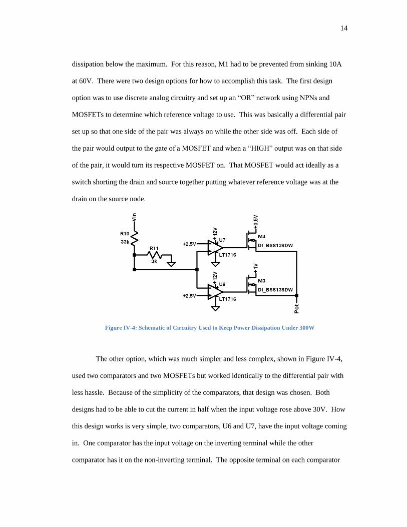
Figure IV-4: Schematic of Circuitry Used to Keep Power Dissipation Under 300W
The other option, which was much simpler and less complex, shown in Figure IV-4,
used two comparators and two MOSFETs but worked identically to the differential pair with
less hassle. Because of the simplicity of the comparators, that design was chosen. Both
designs had to be able to cut the current in half when the input voltage rose above 30V. How
this design works is very simple, two comparators, U6 and U7, have the input voltage coming
in. One comparator has the input voltage on the inverting terminal while the other
comparator has it on the non-inverting terminal. The opposite terminal on each comparator

15
has the reference voltage of 2.5V on it. When the input voltage is between 0V to 30V, U6
would output a logic high voltage while U7 would output a logic low voltage. Once the input
voltage rises above 30V, U6 and U7 change roles and U7 has the logic high output and U6
has the logic low output. The output of each comparator is connected to their respective
MOSFET. The drain of each MOSFET is connected to its respective reference voltage. The
gate of M3 is connected to the output of U6 while the drain is connected to the +1V
reference. When U6 outputs logic high, M3 turns on allowing the +1V reference voltage to
show up at the source node which is connected to the top of the potentiometer. As you recall,
the potentiometer controlled the current through M1 and whatever voltage was at the top of
the potentiometer set the maximum current allowed through M1. Similarly, when U7 outputs
logic high, M4 turns on and M3 turns off allowing the voltage at the drain of M4 to pass to
the source which is also connected to the top of the potentiometer. The difference when M4
turns on, is it has a +0.5V reference voltage attached to the drain that passes to the source
node. This 0.5V now limits the current through M1 to 5A maximum and can maintain the
300W power dissipation requirement because 5A at 60V is only 300W and 10A at 30V is
also 300W not allowing M1 to dissipate more than 300W. With this configuration, there is
no way for the MOSFET to dissipate more power than 300W keeping it under the maximum
specified on the datasheet.
e. Output Buffer Amplifier
Figure IV-5 on page 16 shows the schematic of the buffer amplifier that outputs to
the voltmeter to display the current sinking through M1. This circuit is setup as a simple
buffer op-amp design. The input voltage comes from the wiper of the potentiometer and
feeds the non-inverting terminal of an LT6010 op-amp. The output of the op-amp feeds a
digital multi-meter which displays the voltage at the wiper node. Because the op-amp has no

16
amplification and acts strictly as a buffer, the digital multi-meter was set so that where the
decimal point was placed would allow the maximum voltage of 1.00V to read 10.0V. The
digital multi-meter reads a voltage from 0V to 1V but displays it as a voltage from 0V to
10V. Even though it reads a voltage measurement, it can be directly correlated to the current
measurement through M1 because the voltage dropped across R3 is directly related to the
amount of current through M1.
Figure IV-5: Buffered Output of Current Reading,

17
V. Construction
To keep a high power density with low cost parts and small surface area, surface
mount components were chosen for this project. There were only three components that were
not surface mount components and those were M1, R3, and VTEMP. The layout for this
project was done with ExpressPCB and the printed circuit boards (PCBs) were fabricated by
them. The building of this project was done in multiple phases broken down into the building
of the power regulator circuit, building of the main circuit, fabrication of the heat sinks,
fabrication of the cabling, and then the fabrication of the two remaining modules.
a. Fabricating the Power Regulator Circuit and Main Circuit
These two circuit boards were both straight forward in their build phase. One has to
go one component at a time matching up the layout to the schematic to the PCB and then
soldering the component to the board. There were no special complications that had to be
considered except for maybe the packages with really small pitch. Extra care had to be taken
on those components to ensure no solder bridges were created across the leads. Other issues
arose as modifications had to be made to the PCB without fabricating a new one. Those
fabrication modifications will be described in greater detail in Chapter VI Section A and B.
The finished PCBs with modifications, the Power Regulation Circuit and the Main PCB, can
be seen in Figure V-1 and Figure V-2 respectively.

18
Figure V-1: Finished Power Regulator PCB
Figure V-2: Main PCB Circuit with Modification

19
b. Fabricating the Heat Sinks
The heat sinks were interesting to fabricate because a good thermal connection had to
be made between the MOSFET (M1) and the heat sink to adequately dissipate the 300W of
power. The other issue involved was that M1 had to be mounted on the same heat sink as the
LM35DT so the LM35DT could read the temperature rise generated by the power being
dissipated from M1. The problem with this was the tabs of both the LM35DT and M1 were
different voltage potentials. M1 was at the input voltage potential and the LM35DT was at
the ground potential. Having the input short to ground through these two devices was not
going to work and a solution had to be created.
The original design was to have M1 and Vtemp separated electrically with some
double sided sticky thermal tape. A hole was drilled into the heat sink, one for each TO-220
package, and then a metal screw was screwed into the heat sink through the hole in the
TO-220 package. After much trial and error, it was discovered that the heat sink metal was
stronger than the metal screws and kept breaking the head of the screws off and would not
tighten down on the TO-220 packages allowing for good thermal conductivity. It was also
discovered that the thermal tape did not have very good heat transfer and another approach
was needed.
The next approach used a clamping method for attaching the TO-220 package to the
heat sink. The package was forced to the heat sink by a piece of aluminum stock on top of it.
The aluminum stock was screwed down to the mounting holes of the heat sink causing the
pressure needed to adequately dissipate the heat. It also allowed heat to transfer out of the
plastic part of the case through the aluminum stock to add additional cooling. To keep VTEMP
electrically isolated from M1, VTEMP was epoxied to the heat sink surface where it did not
have metal touching metal. Figure V-3 shows the heat sink with M1 clamped.

20
Figure V-3: Heat Sink with M1 and R3 Attached via Clamping Method
It was also discovered that in order to keep the heat as far away from the surface
mount components as possible, R3 should be pulled off the board and attached to a heat sink.
An electrically isolated resistor from Caddock Electronics Inc. was used and secured to the
heat sink in the same manner as M1. It only had to dissipate a maximum of 10W but instead
of putting in a different kind of resistor or putting a heat sink on the board and connecting this
resistor to it, the electrically isolated property could be exploited and allow this resistor to be
connected to the heat sink.
c. Fabricating the Cabling
The cabling was a more sophisticated part of the design because it had to be able to
connect all three modules together since they all used the same over temperature LED, over
voltage LED, and potentiometer. The cabling was also used to attach each module to the
reference voltages from the power regulation circuit.
21
One aspect out of the scope of this project but for further investigation would be how
to make this easily expandable. Currently, no more than three modules could be used
because of the limited wiring connections that were installed. If more than three modules
were needed, a new wiring harness would have to be fabricated. Now this could be a feasible
option but would not work if the goal was to keep the cost down. Another type of connection
that could be used instead of a wiring harness could be something similar to that of the PCI
slots on computer motherboards. However, there is not any possible way to plan for infinite
modules and at some point a maximum number of modules would have to be specified.
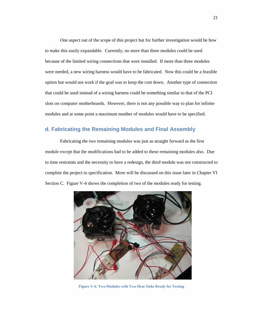
d. Fabricating the Remaining Modules and Final Assembly
Fabricating the two remaining modules was just as straight forward as the first
module except that the modifications had to be added to these remaining modules also. Due
to time restraints and the necessity to have a redesign, the third module was not constructed to
complete the project to specification. More will be discussed on this issue later in Chapter VI
Section C. Figure V-4 shows the completion of two of the modules ready for testing.
Figure V-4: Two Modules with Two Heat Sinks Ready for Testing

22
VI. Testing and Required Modifications
Testing occurred in three phases with the first being the testing of the power regulator
circuit. The next phase was the testing of the individual modules and the final phase being
the testing of multiple modules. Most modifications that were made were done during the
testing of each individual module and few were made when testing multiple modules at once.
The lab testing area can be seen in Figure VI-1.
Figure VI-1: Lab Testing Area

23
a. Testing the Power Regulation Circuit
This circuit was by far the most complicated circuit to keep working and the one with
the most flaws. Numerous issues were encountered in the testing of this design and for this
project to properly meet specifications; a redesign of this circuit would need to be completed.
The first and greatest complication in this design was due to the fact that the linear
regulators were under designed and under specified. These regulators should not be
powering anything that drew a lot of current so there should not be any need for these
regulators to source an amp or more of power. During testing though, only two of the six
regulators would actually regulate their voltage and properly output the correct voltage. A
drop in output voltage was experienced during testing which would most likely be attributed
to a lot of current being sourced. The +5V and +2.5V regulators were only inputs into
comparators and since comparators are essentially op-amps, the current into the inverting or
non-inverting terminals is ideally equal to zero. Now the +5V rail was also used to power the
three LEDs used but that was designed to be no more than 50mA between the LEDs and the
+5V rail could handle 250mA. Along those same lines, the ±12V rails could not hold at their
12V level and the +12V rail was about half of what it should be. The ±12V rails were only
used to power the different op-amps and comparators and should have only been pulling
micro-amps each. The +1V and +0.5V regulators were the only ones that could maintain
their output voltage. These regulators should have been sufficient with the little amount of
current being pulled through them but somehow they still could not maintain their output
voltage.
Other evidence that showed too much current was being pulled through the linear
regulators was that the -12V regulator was getting almost too hot to touch meaning that a
sufficient amount of power was being dissipated in that package. One of the op-amps that the

24
rail was powering was pulling a lot of current but there was no simple way to determine
which one without pulling each chip off the board or cutting traces to determine how much
current was being drawn. No op-amp got warm from the current draw. That current was
going somewhere but it was indeterminate as to where it was going.
If this project was to be continued and a second version was to be created, the power
regulation circuitry would need to be redesigned. One frustrating part of this design was the
variation in the socket sizes in the regulator chips. Not only were package sizes chosen that
were not compatible with any other manufacturer other than the one used but most were too
small to carry enough current. With the redesign of the power regulation circuit, new linear
regulators would be chosen that could handle higher current and would be standardized to
one chip size if possible. When redesigned, it would be required that each regulator be able
to source close to an amp of current. Even though it may not be needed, that would ensure
the beefiness of the regulator chips. The SOIC package was sufficient to carry about an amp
but it would probably be better to put TO-220 packaged linear regulators that are guaranteed
to carry an amp and then work it out to put each of them on one heat sink to dissipate the
heat.
Another redesign desperately needed on the power regulation board was a connector
addition. Each of the six regulators, two leads for the power LED, a lead for the temperature
reference, a lead to power the LCD voltmeter, a number of ground leads, plus fan power leads
(which were never attached to this board) all needed to be connected to this PCB. All the
cables that were oversights did not even have a through hole connection on the board. The
ground connection, for instance, was soldered to the ground plane on the bottom of the
circuit. With all those cables connected to the board, there was not much room to maneuver
around the board for testing, troubleshooting, and replacement of parts without first removing

25
some or all of the cables. To assist in not only the simplicity of the board but also in the
availability of the board, all the cables on and off of that board would need to be added to a
connector that could allow the cabling to be removed for troubleshooting purposes.
b. Testing of the Single Module
This testing phase was the most complicated of all the phases and took the most
amount of time to complete. Testing occurred until the very end and was really never
completed. One thing learned during this phase that will never be forgotten, is that not all
potentiometers are wired the same way and the schematic for the potentiometer needs to be
paid attention to so that the project will work.
The first issue encountered was actually getting the potentiometer wired correctly so
the load would function as desired. What was occurring was when the potentiometer would
change, the current would not move at all until the potentiometer would get turned
completely clockwise. By turning the potentiometer completely clockwise gave little enough
resistance across the potentiometer that a voltage was placed on the non-inverting terminal of
U8 allowing current to flow through M1. The problem with that was the power supply being
tested was not specified to handle 10A let alone 2.5A and therefore was also causing havoc
with the power supply. When this circumstance was encountered, the amount of current
pulled from the power supply under test was about 2.5A. After the potentiometer was wired
correctly, the load started acting correctly where the current followed the changing of the
potentiometer.
After getting the unit to work correctly, the testing of each module was simple
because if the current adjusted with the potentiometer then the module worked. However,
there are many other functions of this module and they need to be tested as well to prove that
this module really works as designed. The tests were broken down into:

26
Will the electronic load sink current?
Will the electronic load not let the current rise above the max current of 10A under
30V or 5A under 60V?
Will the electronic load switch the current reference voltages at or just above 30V?
Will the electronic load shut off if the Device Under Test (DUT) output voltage rises
above 60V?
Will the electronic load shut off if the temperature rises above 80°C?
If each one of those questions could be answered with a “yes,” then the module was
concluded that it worked and set aside for the multiple module testing.
With that testing in mind, each module tested made it to a maximum current of 8.68A
but could not go higher due to the potentiometer voltage not going higher than 0.868V.
Every other aspect tested worked fine. There were still some bugs to work out but the
functions of each piece of protection and the unit in general worked pretty much as expected.
Table VI-1below shows the data gathered from the testing of the single module. Something
occurred from the time the first full current data was gathered and the second full current data
was gathered. As evidenced below, the full load current no longer shows 8.68A. Now that
was an actual current reading but could not be reproduced a couple of days later. For the
reader’s reference, every value shown in the table represents the load current gathered from
different sources and points on the circuit. The wiper voltage will show the theoretical
current reading if multiplied by a factor of ten.
To talk a little about the data shown in the table, none of the current readings match
up. Each column in this table should show about the same number along a row. For instance,
the top row with 100% load, should read about 5.44A all the way across that row. When
these measurements were taken the first time, that was the case. When they were looked at

27
during a later date, these values did not track and that discrepancy was not determined. This
discrepancy will also show itself later in the two module data in Chapter VI, Section C. All
future discussion of the max current, will be dictated from the first max current value of
8.68A.
Table VI-1: Collected Data from Single Module Testing
Percent Load
Actual Load
Current (A)
Calculated Load Current from
Source Voltage (A)
Current Reading from Built in
Meter (A)
Wiper Voltage (V)
100% 5.44 6.24 7.38 0.73
90% 5.03 5.75 6.48 0.64
80% 4.43 5.05 5.78 0.57
70% 3.93 4.5 5.22 0.52
60% 3.35 3.82 4.56 0.45
50% 2.79 3.19 3.9 0.39
40% 2.23 2.55 3.14 0.31
30% 1.68 1.91 2.29 2.27
20% 1.16 1.32 1.53 0.15
If the maximum current sunk was only 8.68A and the desired current was 10A, then
something needed to be changed to get the maximum desired current. As discussed earlier,
the amount of current sunk is determined by the voltage seen on the wiper of the
potentiometer. If the wiper voltage never reaches 1V, then the current will never reach 10A.
This was occurring with the modules and was the reason that the max current was never
reached.
This issue was believed to be because of M3 and M4. Since they are MOSFETs,
they act like a resistor when conducting and these particular MOSFETs have an on resistance
of 1.4Ω. Following Ohm’s Law, there will be a voltage drop across these MOSFETs if there
is current flowing. The current measured through the potentiometer was only 16µA with the
load drawing full current and at 1.4Ω the voltage drop would be in the microvolt range which

28
does not account for the voltage drop experienced. Coming out of the regulator, there was
0.998V and the voltage measured at the top of the potentiometer was 0.868V. It was even
noticed that at the drain of the MOSFET, there was 0.998V but at the source there was
0.868V. The little amount of current measured does not seem to account for the missing
voltage but then Ohm’s Law cannot be wrong either. Something has to account for the
voltage drop.
To further troubleshoot this issue, the +1V regulator line was disconnected from the
regulator and attached to a lab bench variable power supply. The voltage was then measured
at the source of the MOSFET and at the drain of the MOSFET. The voltage on the variable
power supply was then increased. The voltage measured at the drain followed the voltage of
the power supply. The voltage at the source increased some, but only hundreds of milli-volts.
There was never a significant enough increase on the source compared to the drain which was
very surprising. Theoretically, the voltage on the drain and on the source should have both
gone up somewhat proportionately if the MOSFET were truly acting like a switch. This was
one mystery that never could be figured out and it was just assumed that for some reason the
voltage was lost from drain-source but unclear why there was so much of a voltage drop.
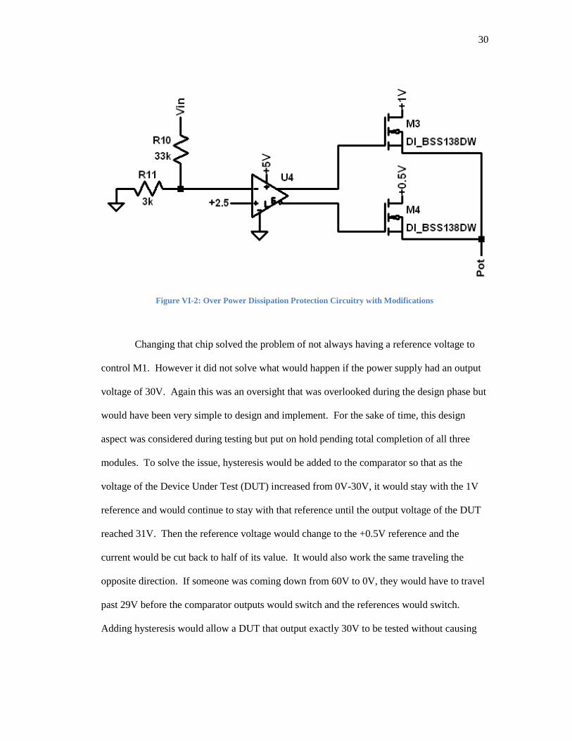
The major modification that had to be made to this circuit was to the protection
circuitry that kept M1 from dissipating too much power. The problem that was occurring was
when the input voltage rose above 30V, the comparator that handled the 30V-60V range
would not turn on but the other comparator would turn off and then there was no reference
voltage to tell current to flow through M1. To solve this issue, a comparator that had an
output and the opposite of that output was used. There are two outputs, one that will be
called simply “output” and the other that will be called “not-output.” The way these two

29
outputs work is if one is outputting VHIGH, the other is outputting VLOW. This became a way
to ensure that both M3 & M4 received a voltage at the gate so they knew how to act.
Some issues arose from making this change. First, the PCB was set up to handle two
SOT-23-5 packages for the two comparators in the original design. Four of the six pins from
the SOT-23-5 package were the same as four pins from the SOT-23-6 package the new
comparator came in. The other two pins were more complicated to use and modifications had
to be made to use those pins. It was easier to solder bridge the second output to the correct
gate because the pin on the SOT-23-6 package was right next to the trace that took the output
from the second comparator, in the original design, to its respective MOSFET. Second, this
comparator would not allow a VCC greater than +5V. Therefore, the +12V rail had to have
the trace cut so as not to conduct to the chip while also bringing a wire around from the
closest +5V rail to the VCC pin. To make matters worse that pin had no pad to solder to
because the new package was an SOT-23-6 meaning that there were six pins in the new
package opposed to the five in an SOT-23-5. Third, the pitch of an SOT-23-6 was about half
the width of the original comparator’s pitch so some tricky placing was done to get the chip
in place. The task at hand was accomplished and the new comparator was implemented and
worked correctly.
30
Figure VI-2: Over Power Dissipation Protection Circuitry with Modifications
Changing that chip solved the problem of not always having a reference voltage to
control M1. However it did not solve what would happen if the power supply had an output
voltage of 30V. Again this was an oversight that was overlooked during the design phase but
would have been very simple to design and implement. For the sake of time, this design
aspect was considered during testing but put on hold pending total completion of all three
modules. To solve the issue, hysteresis would be added to the comparator so that as the
voltage of the Device Under Test (DUT) increased from 0V-30V, it would stay with the 1V
reference and would continue to stay with that reference until the output voltage of the DUT
reached 31V. Then the reference voltage would change to the +0.5V reference and the
current would be cut back to half of its value. It would also work the same traveling the
opposite direction. If someone was coming down from 60V to 0V, they would have to travel
past 29V before the comparator outputs would switch and the references would switch.
Adding hysteresis would allow a DUT that output exactly 30V to be tested without causing

31
the comparator to get confused because the comparator would have to wait until 31V before it
switched references.
It was also decided that hysteresis would need to be added to the other comparators to
assist in their functions. But due to time and decreased flexibility from a prebuilt PCB and
surface mount components, hysteresis was not added to the other comparators either.
When testing the over voltage and over temperature protection, both protections
worked as designed with the exception that the LEDs showed the protections as active before
they were. As the comparator started changing because the voltage level was getting close to
the reference voltage, the LEDs would start to turn on. They started out dimly at first but got
to full brightness when the comparator turned on hard. This was strange because they were
expected to remain off until the comparator fully switched over instead of getting some
residual voltage and current on them to turn on early. Originally an NPN transistor was being
used thinking it would not turn on because there was ideally 0V on the output of the
comparator and it would need to be at least 0.7V above ground before it would turn the
transistor on. When the comparator switched to VHIGH, then the transistor would turn on.
Thinking that maybe the VLOW of the comparator was close to the 0.7V turn-on voltage of the
NPN, it was decided to try using a MOSFET because it would have a higher gate-source
voltage or turn-on. With the gate-source voltage being 1.2V, the comparator would in no
way be able to turn the MOSFET on and there would be no current flow through it to allow
the LED to turn on. Again, mysteriously, the LED turned on with the MOSFET.
The way a comparator works is if the reference is on the inverting input and the input
voltage is on the non-inverting input, then the comparator output will follow what the input is
doing. Basically, if the input is below 5V, the reference voltage, then it will output VLOW and
when the voltage crosses over the 5V threshold, the output switches to VHIGH. It is not a

32
gradual or linear change but an instant change when the input is exactly at 5V. It works very
similar to a square wave. For this MOSFET or NPN to be turning on enough for current to
flow is rather mysterious and more thought and time would also be necessary to resolve this
issue.
One very important change in a redesign of the main circuit is changing where the
current measurement is read from. The voltmeter that displays how much current is being
sunk through M1 is reading its measurement off of the wiper of the potentiometer. Now this
is somewhat acceptable because ideally that voltage is the current through M1. But to be
more exact, the current measurement should be taken off the source node of M1. That
voltage is the voltage drop across R3 which is exactly related to the current through M1 based
on Ohm’s Law. The change in a redesign would be a very simple task to move the trace and
would greatly improve accuracy of the current meter.
One issue discovered and partially mentioned earlier was that R3 was just a giant
through hole resistor and was mounted directly on the board. This was alright because it
could handle the power that would be dissipated by the resistor but the heat dissipated by it
would be horrible and that would leave a lot of heat directly on the board. It was decided that
an electrically isolated resistor that could be mounted on the heat sink would be a better
choice. An electrically isolated resistor was found from Caddock Electronics Inc. that came
in a TO-220 style package and was completely isolated from the metal of the heat sink. This
became a very efficient way of dissipating the heat from R3 because it could use the heat sink
M1 used which was more than adequate enough to dissipate the heat of both devices.
As discussed earlier, VTEMP had to be isolated from the heat sink as well because the
tab of M1 was connected to the drain which would be a varying voltage and the tab of VTEMP
was connected to ground. Since these two tabs could not be connected, it was decided to try
33
some electrically isolating double sided thermal tape. That tape was cut easily by the sharp
corners of the tab on VTEMP and therefore VTEMP was epoxied to the heat sink with the tab in
the air electrically isolated from the heat sink. This method was never implemented
permanently in the design because it was unclear how the modules would be mounted in the
enclosures and it was undesirable for it to be mounted to the heat sink in case a modification
needed to be made.
c. Testing Two Modules
This testing actually went much better than expected and surprisingly the modules
performed better than expected. Had enough time been available to build and test the third
module, it is expected to have worked also and it is expected to have worked with the other
two modules. Several obstacles interfered with building the third module. When the first two
modules were tested together, the max current sunk into the load was about 12A. That was
only 2A more than was supposed to be sunk with one module and this required two modules
to sink that amount of current. Adding a third module would not get the max current up to
30A. It probably would not even get the max current to 20A because the power regulation
circuitry was under designed and could not withstand the added current draw from the added
modules. If each module had its own power regulation circuitry, then maybe the max current
could have gotten closer to 30A. It would have been acceptable to see it at 25A but barely
12A after only two modules meant that a major redesign in the power regulation circuitry
needed to be performed before it was feasible to add a third module.
The data collected for the testing of the two modules is shown below in Table VI-2.
Similar discrepancies can be seen in this data as with the single module data. For some
reason, the current measured from multiple points on the circuit do not add up to be the same
or similar currents. As one can see from the “Current Reading from Built in Meter (A)”

34
column, the current through both modules would be 11.7A where the actual current measured
is 16.5A. The actual current measurement is taken from three 0.1Ω put in parallel and the
voltage measured across them. That calculation gives the “Actual Load Current (A)” column.
With the evidence of these discrepancies, a meter that could measure up to 30A would really
be needed to accurately verify the current measurements. Why the measurements from other
areas on the circuit do not add up exaggerates the mystery of the different currents. One of
the reasons for the discrepancy is that the three resistors in parallel are in series with M1 and
R3 and could be altering the effects of R3 as a current sense causing different current to flow.
Theoretically, they should not interfere with the current flow and only affect the voltage drop;
they could be creating some other interesting affects. For purposes of this report, the original
maximum current data stated before this data was gathered will be the data used throughout
the report.
Table VI-2: Data Collected from Two Module Testing
Percent Load
Actual Load
Current (A)
Calculated Load Current from Source Voltage of
Single Module (A)
Current Reading from Built in
Meter (A)
Wiper Voltage
(V)
Total Calculated Load from
Source Voltage
100% 16.545 8.99 5.85 0.572 17.98
90% 15.030 8.3 4.5 0.438 16.6
80% 13.152 7.35 3.67 0.356 14.7
70% 11.667 6.5 3.08 0.299 13
60% 10.061 5.64 2.63 0.255 11.28
50% 8.424 4.64 2.17 0.21 9.28
40% 6.636 3.69 1.72 0.167 7.38
30% 5.030 2.77 1.29 0.125 5.54
20% 3.333 1.82 0.87 0.085 3.64
Along with the power regulation circuitry not being able to handle the added
modules, M3 and M4 on each module had a major voltage drop. This issue ties in with the
linear regulators not being able to supply enough current for the needs of the project. With

35
one module, there was not much voltage drop and the max current sinkable was 8.5A. When
a second module was connected, the max sinkable current per module was 5.6A. It is
believed that if a third module were added, the max sinkable current per module would be
around 3.5A or even lower. It would be hopeful that adding a third module would increase
the max allowable current to be around 15A but it is possible that adding a third module
would do the negative of that. For these reasons and the lack of time, it was decided to leave
these modifications for the first revision of this electronic load.
Another issue that was discovered with the addition of multiple modules was that
there was no way to measure the total current sunk into the load because the measuring point
was being tapped off the wiper of the potentiometer. As discussed earlier, this was already an
errant way of measuring the current because it only dictated what the theoretical current
should be, not the actual current. The modification mentioned earlier would need to be added
to each module and then each reading tied together to one circuit that could output to the
digital voltmeter. The simplest and most straight forward approach to adding all the voltage
readings from each module would be to put them into a multi-input summing op-amp. Then
each modules voltage could be added together and that summed voltage would be the
accurate current reading being sunk through the electronic load as a whole.
At this current time, the voltmeter is reading a voltage off of every module
simultaneously. This means that the node where the meter connects on an individual module
is connected to every other module at the same time. Assuming that every module is
adjusting the current at exactly the same rate, then the meter would read only the current of
one module. That number would have to be multiplied by the number of modules to get the
total current through the system. With a summing junction, the current from each module
would be added together and then the number on the meter would be the actual current.

36

37
VII. Conclusions and Recommendations
After designing and attempting to build a three module electronic load, it is feasible
to conclude that a modular load with more modules could also be functional. There were
definitely complications that were encountered in this design and with more time and
resources this design could be fully capable of meeting its specifications. The potential that
was shown with one module was well accepted and showed that the future expansion of this
design for multiple modules would be entirely possible.
It would be recommended, though, that during a redesign, the power regulation
circuitry be updated and designed to handle the current draw from the additional modules
being placed in parallel. It would also be recommended that the modifications set forth
previously in Chapter VI, for the single module and multiple module design, be implemented
to allow for better form and function in the loading of the DUT.

38
VIII. Bibliography
1. Bryant, James. Ask The Applications Engineer -6. Analog Devices. [Online] 1991.
http://www.analog.com/library/analogDialogue/Anniversary/6.html.
2. Linear Technology. LT1351 - 250mA, 3MHz, 200V/ms Operational Amplifier. Linear
Technology. [Online] 1996. http://cds.linear.com/docs/Datasheet/1351fa.pdf.
3. STMicroelectronics. STW26NM50. STMicroelectronics. [Online] 2009.
http://www.st.com/stonline/books/pdf/docs/8291.pdf.

39
IX. Appendices
A. Schematic
The following pages 31 through 33 are the schematics generated for this project.

40
Figure IX-1: Full Schematic of Original Module Design

41
Figure IX-2: Full Schematic of Designed Module with Modifications

42
Figure IX-3: Schematic of Power Regulation Circuitry

43
B. Circuit Board Layout
Figure IX-4: PCB Layout of Single Module

44
C. Bill of Materials
Table C-I: Main Circuit Bill of Materials
Schematic Number
Quantity Digi-key Part Number Description
Main Circuit
M2/M3/M4/M5 2 BSS138DW-FDICT-ND 2-N Ch., 50V, 3.5mOhm, 200mA, 200mW
M6/M7 2 2N7002-TPMSCT-ND MOSFET N-CH 115MA 60V
U6/U7 1 ADCMP604BKSZ-REEL7CT-ND
Rail-to-Rail, Very Fast, 2.5 V to 5.5 V, Single-Supply LVDS Comparators
M1 1 497-3264-5-ND N-Ch., 500V, 120mOhm, 30A, 313W
U8 1 LT1351CS8-ND 250mA, 3MHz, 200V/ms
U1/U3 2 LT6010CS8-ND 135mA, 14nV/√Hz, Rail-to-Rail Output Precision
U2/U5 2 LT1716HS5#TRMPBFTR-ND
SOT-23, 44V, Over-the-Top, Micropower, Precision Rail-to-Rail Comparator
R1/R2/R4/R14/R19 5 RHM1.00KAECT-ND 1kOhm, thick film, 1/4W, 1%
R3 1 MP930-0.10F-ND RESISTOR 0.10 OHM 30W 1% TO-220
R5 1 RHM10.0KCRCT-ND 10kOhm, thick film, 1/8W, 1%
R12 1 P4.02KCCT-ND 4.02kOhm, thick film, 1/8W, 1%
R10 1 PT33KXCT-ND 33kOhm, thick film, 1W, 1%
R11 1 RHM3.30KCCT-ND 3.3kOhm, thick film, 1/8W, 1%
R6/7 1 3590S-1-104L-ND 100k, wire wound, 2W, 5%, 10 turn
R20 1 P806CCT-ND 806Ohm, thick film, 1/8W, 1%
R21/R25 2 541-100KCCT-ND 100kOhm, thick film, 1/8W, 1%
C1 1 399-1142-1-ND 470pF, 50V, 10%, Ceramic, X7R
C2/C6 2 478-3755-1-ND .1uF, 25V, 10%, Ceramic, X7R
LD2 1 350-2117-ND Red, 3.94mm Panel Mount, 2V
LD3 1 350-1592-ND Blue, 3.94mm Panel Mount, 3.5V
VTEMP 1 LM35DT-ND 4-30V, 0-100C, voltage
Male Connector 1 A32484-ND 16 pins, 2 rows, right angle
Female Connector 1 A25579-ND 16 pins, 2 rows, crimp
Pins 16 A100828CT-ND 16-20 AWG, Tin
Vin Male Connector 1 WM1041-ND CONN HEADER 2POS .093 VERT TIN
Vin Female Connector
1 WM1671-ND CONN RECEPTACLE 2POS .093
Pins 2 WM1101-ND 14-20 AWG, Tin, Female
Potentiometer Knob 1
45
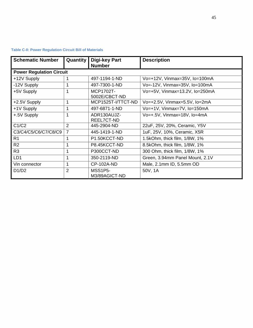
Table C-II: Power Regulation Circuit Bill of Materials
Schematic Number Quantity Digi-key Part Number
Description
Power Regulation Circuit
+12V Supply 1 497-1194-1-ND Vo=+12V, Vinmax=35V, Io=100mA
-12V Supply 1 497-7300-1-ND Vo=-12V, Vinmax=35V, Io=100mA
+5V Supply 1 MCP1702T-5002E/CBCT-ND
Vo=+5V, Vinmax=13.2V, Io=250mA
+2.5V Supply 1 MCP1525T-I/TTCT-ND Vo=+2.5V, Vinmax=5.5V, Io=2mA
+1V Supply 1 497-6871-1-ND Vo=+1V, Vinmax=7V, Io=150mA
+.5V Supply 1 ADR130AUJZ-REEL7CT-ND
Vo=+.5V, Vinmax=18V, Io=4mA
C1/C2 2 445-2904-ND 22uF, 25V, 20%, Ceramic, Y5V
C3/C4/C5/C6/C7/C8/C9 7 445-1419-1-ND 1uF, 25V, 10%, Ceramic, X5R
R1 1 P1.50KCCT-ND 1.5kOhm, thick film, 1/8W, 1%
R2 1 P8.45KCCT-ND 8.5kOhm, thick film, 1/8W, 1%
R3 1 P300CCT-ND 300 Ohm, thick film, 1/8W, 1%
LD1 1 350-2119-ND Green, 3.94mm Panel Mount, 2.1V
Vin connector 1 CP-102A-ND Male, 2.1mm ID, 5.5mm OD
D1/D2 2 MSS1P5-M3/89AGICT-ND
50V, 1A