Modul AA103 Mitsubishi Q Series IO Module type.PDF
92
I/O Module Type Building Block User's Manual User's Manual Mitsubishi Programmable Logic Controller I/O Module Type Building Block
-
Upload
ahmad-lazuardi -
Category
Documents
-
view
22 -
download
4
Transcript of Modul AA103 Mitsubishi Q Series IO Module type.PDF

I/O M
od
ule
Typ
e B
uild
ing
Blo
ck Use
r's Ma
nu
al
U
User's Manual User's Manual
Mitsubishi Programmable Logic Controller
When exported from Japan, this manual does not require application to theMinistry of International Trade and Industry for service transaction permission.
Specifications subject to change without notice.
HEAD OFFICE : MITSUBISHI DENKI BLDG MARUNOUCHI TOKYO 100-8310 TELEX : J24532 CABLE MELCO TOKYONAGOYA WORKS : 1-14 , YADA-MINAMI 5 , HIGASHI-KU, NAGOYA , JAPAN
MODEL
MODELCODE
Q-IO-U-E
13JL99
SH(NA)-080042-D(0007)MEE
I/O Module Type Building BlockI/O Module Type Building Block
A - 1 A - 1
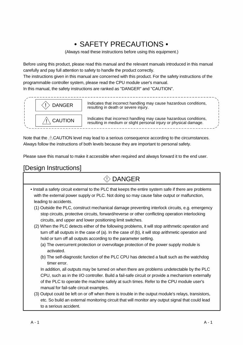
• SAFETY PRECAUTIONS • (Always read these instructions before using this equipment.)
Before using this product, please read this manual and the relevant manuals introduced in this manual carefully and pay full attention to safety to handle the product correctly. The instructions given in this manual are concerned with this product. For the safety instructions of the programmable controller system, please read the CPU module user's manual. In this manual, the safety instructions are ranked as "DANGER" and "CAUTION".
! DANGER
CAUTION!
Indicates that incorrect handling may cause hazardous conditions,resulting in death or severe injury.
Indicates that incorrect handling may cause hazardous conditions, resulting in medium or slight personal injury or physical damage.
Note that the ! CAUTION level may lead to a serious consequence according to the circumstances. Always follow the instructions of both levels because they are important to personal safety. Please save this manual to make it accessible when required and always forward it to the end user. [Design Instructions]
! DANGER • Install a safety circuit external to the PLC that keeps the entire system safe if there are problems
with the external power supply or PLC. Not doing so may cause false output or malfunction, leading to accidents. (1) Outside the PLC, construct mechanical damage preventing interlock circuits, e.g. emergency
stop circuits, protective circuits, forward/reverse or other conflicting operation interlocking circuits, and upper and lower positioning limit switches.
(2) When the PLC detects either of the following problems, it will stop arithmetic operation and turn off all outputs in the case of (a). In the case of (b), it will stop arithmetic operation and hold or turn off all outputs according to the parameter setting. (a) The overcurrent protection or overvoltage protection of the power supply module is
activated. (b) The self-diagnostic function of the PLC CPU has detected a fault such as the watchdog
timer error. In addition, all outputs may be turned on when there are problems undetectable by the PLC CPU, such as in the I/O controller. Build a fail-safe circuit or provide a mechanism externally of the PLC to operate the machine safely at such times. Refer to the CPU module user's manual for fail-safe circuit examples.
(3) Output could be left on or off when there is trouble in the output module's relays, transistors, etc. So build an external monitoring circuit that will monitor any output signal that could lead to a serious accident.

A - 2 A - 2
[Design Instructions]
! DANGER • When overcurrent exceeding the rated load current or caused by a shorted load or the like flows
in the output module for a long time, it may cause smoke or fire. To prevent this, configure an external safety circuit, such as fuses.
• Build a circuit that turns on the external power supply after the PLC power supply has been turned on. If the external power supply is turned on first, it could result in false output or malfunction.
• When there are communication problems with the data link, refer to the corresponding data link manual for the operating status of each station. Not doing so could result in false output or malfunction.
• When connecting a peripheral device to the CPU module or connecting a personal computer or the like to the intelligent function module to exercise control (data change) on the running PLC, configure up an interlock circuit in the sequence program to ensure that the whole system will always operate safely. Also before exercising other control (program change, operating status change (status control)) on the running PLC, read the manual carefully and fully confirm safety. Especially for the above control on the remote PLC from an external device, an immediate action may not be taken for PLC trouble due to a data communication fault. In addition to configuring up the interlock circuit in the sequence program, corrective and other actions to be taken as a system for the occurrence of a data communication fault should be predetermined between the external device and PLC CPU.
! CAUTION • Do not bundle the control wires or communication cables with the main circuit or power wires, or
run them close to each other. They should be run 100mm (3.94in.) or more away from each other. Not doing so could result in noise that would cause malfunction.
• When the output module is used to control a lamp load, heater, solenoid valve or the like, large current (approximately 10 times greater than the normal) may flow when the output is turned from OFF to ON. Choose an output module having a sufficient rated current.

A - 3 A - 3
[Installation Instructions]
! CAUTION • Use the PLC in the environment that meets the general specifications given in this manual.
Using this PLC in the environment outside the range of the general specifications could result in electric shock, fire, malfunction, or damage to, or deterioration of the product.
• Hold down the module-loading lever at the module bottom, and securely insert the module-fixing hook into the fixing hole in the base unit. Incorrect loading of the module can cause a malfunction, failure or drop. When using the PLC in the environment of much vibration, tighten the module with a screw. Tighten the screw in the specified torque range. Undertightening can cause a drop, short circuit or malfunction. Overtightening can cause a drop, short circuit or malfunction due to damage to the screw or module.
• When installing extension cables, be sure that the connectors of base unit are installed correctly. After installation, check them for looseness. Poor connections could cause an input or output failure.
• Securely load the memory card by pushing it into the memory card loading connector. After loading, make a check. Not doing so can cause malfunction due to a contact fault.
• Completely turn off the external power supply before loading or unloading the module. Not doing so could result in damage to the product.
• Do not directly touch the module's conductive parts. Doing so could cause malfunction or failure of the module.
[Wiring Instructions]
! DANGER • Completely turn off the external power supply before starting wiring. Not doing so could result in
electric shock or damage to the product.
• When turning on the power supply or starting operation after wiring work, always mount the product with the supplied terminal cover. Not doing so could result in electric shock.

A - 4 A - 4
[Wiring Instructions]
! CAUTION • Always ground the FG and LG terminals to the protective ground conductor. Not doing so could
result in electric shock or malfunction.
• Before wiring the module, confirm the rated voltage and terminal layout of the product. Connecting a power supply that is different from the rating or incorrectly wiring the product could result in fire or failure.
• External connectors should be crimped or pressure-welded with the specified tools, or correctly soldered. Imperfect connections could result in short circuit, fires or malfunction.
• Tighten the terminal screws in the specified torque range. Undertightening could result in short circuit, fire or malfunction. Overtightening could cause damage to the screws and/or the module, resulting in drop, short circuit or malfunction.
• Be careful not to allow foreign matter such as chips and wire off-cuts to enter the module. Foreign matter could cause fire, failure, or malfunction.
• The module has an ingress prevention label on its top to prevent foreign matter, such as wire offcuts, from entering the module during wiring. Do not peel this label during wiring. Before starting system operation, be sure to peel this label because of heat dissipation.
[Startup/Maintenance Instructions]
! DANGER • Do not touch the terminals while power is on.
Doing so could cause electric shock.
• Correctly connect the battery. Do not charge, disassemble, heat, place in fire, short circuit, or solder the battery. Mishandling of the battery can cause heat generation, burst or ignition which could result in injury or fire.
• Always turn off the external power supply completely before cleaning the module or retightening the terminal or module mounting screws. Not doing so could result in electric shock. Undertightening of terminal screws can cause a short circuit or malfunction. Overtightening of screws can cause damage to the screws and/or the module, resulting in drop, short circuit, or malfunction

A - 5 A - 5
[Startup/Maintenance Instructions]
! CAUTION • The online operations conducted for the running CPU module by connecting a peripheral device
(especially program modification, forced output, operating status change) should be performed after you have read the manual carefully read and fully confirmed safety. Operation mistakes could cause machine damage or accident.
• Do not disassemble or modify the modules. Doing so could cause failure, malfunction, injury or fire.
• Always switch off the external power supply completely before mounting or removing the module. Not doing so can cause failure or malfunction of the module.
• Before touching the module, always touch grounded metal, etc. to discharge static electricity from human body, etc. Not doing so can cause the module to fail or malfunction.
[Disposal Instructions]
! CAUTION • When disposing of this product, treat it as industrial waste.

A - 6 A - 6
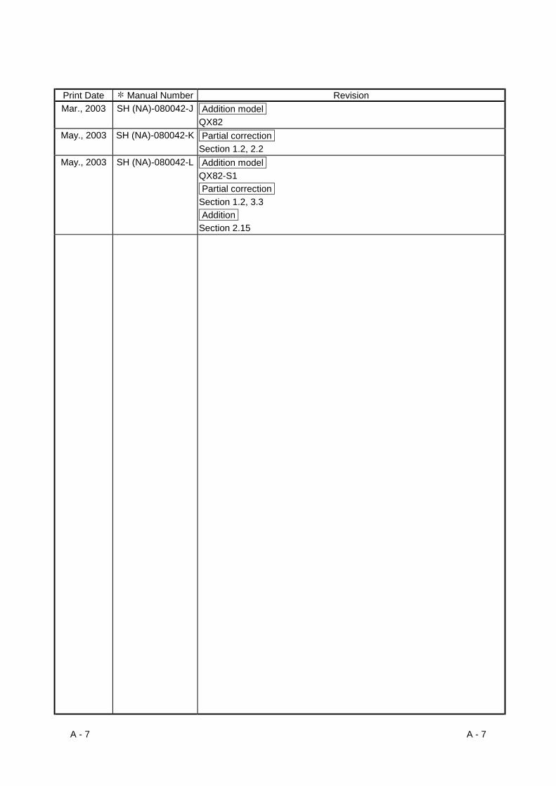
REVISIONS
The manual number is given on the bottom left of the back cover. Print Date Manual Number Revision Dec., 1999 SH (NA)-080042-A First edition Feb., 2000 SH (NA)-080042-B Addition model
QH42P, QX48Y57, QX70, QX71, QX72, QY18A Addition Chapter 4 Partial correction Section 1.2, Chapter 5, 8.1, Chapters 4 to 8 (changed into Chapters 5 to 9)
Apr., 2000 SH (NA)-080042-C Deletion QY18A
Jul., 2000 SH (NA)-080042-D Addition model QX28,QX40-S1,QY18A,QY22,QI60 Addition Chapter 5 Partial correction Section 1.2 Chapters 5 to 9 (changed into Chapters 6 to 10)
Nov., 2000 SH (NA)-080042-E Addition model QY70, QY71 Addition Section 1.3 Partial correction CONTENTS, Section 3.3, 5.1
Jan., 2001 SH (NA)-080042-F Addition model QY68A Addition Section 10.2 Partial correction CONTENTS, Section 1.2, 3.3, 5.1, Chapters 7
Mar., 2001 SH (NA)-080042-G Partial correction Section 2.4, 8.1
Jul., 2001 SH (NA)-080042-H Addition model Q6TE-18S Addition Chapter 9, APP 1.3 Partial correction CONTENTS, Section 2.1, 2.2, 2.4, 5.1 Chapters 9 to 10 (changed into Chapters 10 to 11)
Jul., 2002 SH (NA)-080042-I Addition model QX41-S1, QX42-S1, A6CON4
Japanese Manual Version SH-080024-L
This manual confers no industrial property rights or any rights of any other kind, nor does it confer any patent licenses. Mitsubishi Electric Corporation cannot be held responsible for any problems involving industrial property rights which may occur as a result of using the contents noted in this manual.
1999 MITSUBISHI ELECTRIC CORPORATION
A - 7 A - 7
Print Date Manual Number Revision Mar., 2003 SH (NA)-080042-J Addition model
QX82 May., 2003 SH (NA)-080042-K Partial correction
Section 1.2, 2.2 May., 2003 SH (NA)-080042-L Addition model
QX82-S1 Partial correction Section 1.2, 3.3 Addition Section 2.15

A - 8 A - 8
INTRODUCTION
Thank you for choosing the MITSUBISHI MELSEC-Q Series General-Purpose Programmable Logic Controller. Before using this product, please read this manual carefully to use the equipment to its optimum.
CONTENTS
About Manuals ..............................................................................................................................................A- 10
1. GENERAL SPECIFICATIONS OF INPUT AND OUTPUT MODULES AND INSTRUCTIONS FOR SELECTING THEM 1- 1 to 1- 12
1.1 General Specifications ............................................................................................................................ 1- 1 1.2 Selecting Instructions.............................................................................................................................. 1- 1 1.3 How to Make Settings on GX Developer................................................................................................. 1- 8
1.3.1 Setting of I/O response time ............................................................................................................. 1- 8 1.3.2 Setting of error-time output mode..................................................................................................... 1-10 1.3.3 QI60 switch setting............................................................................................................................ 1-11
2. INPUT MODULE SPECIFICATIONS 2- 1 to 2-18
2.1 QX10 AC Input Module........................................................................................................................... 2- 1 2.2 QX28 AC Input Module........................................................................................................................... 2- 2 2.3 QX40 DC Input Module (Positive Common Type)................................................................................. 2- 3 2.4 QX40-S1 DC Input Module (Positive Common Type) ........................................................................... 2- 4 2.5 QX41 DC Input Module (Positive Common Type)................................................................................. 2- 5 2.6 QX41-S1 DC Input Module (Positive Common Type) ........................................................................... 2- 6 2.7 QX42 DC Input Module (Positive Common Type)................................................................................. 2- 8 2.8 QX42-S1 DC Input Module (Positive Common Type) ........................................................................... 2- 9 2.9 QX70 DC Input Module (Positive Common/Negative Common Shared Type) .................................... 2-11 2.10 QX71 DC Input Module (Positive Common/Negative Common Shared Type).................................. 2-12 2.11 QX72 DC Input Module (Positive Common/Negative Common Shared Type).................................. 2-13 2.12 QX80 DC Input Module (Negative Common Type) .............................................................................. 2-14 2.13 QX81 DC Input Module (Negative Common Type) .............................................................................. 2-15 2.14 QX82 DC Input Module (Negative Common Type) .............................................................................. 2-16 2.15 QX82-S1 DC Input Module (Negative Common Type) ........................................................................ 2-17
3. OUTPUT MODULE SPECIFICATIONS 3- 1 to 3- 13
3.1 QY10 Contact Output Module ................................................................................................................ 3- 1 3.2 QY18A Contact Output Module (All Points Independent) ..................................................................... 3- 2 3.3 QY22 TRIAC Output Module.................................................................................................................. 3- 3 3.4 QY40P Transistor Output Module (Sink Type) ...................................................................................... 3- 4 3.5 QY41P Transistor Output Module (Sink Type) ...................................................................................... 3- 5 3.6 QY42P Transistor Output Module (Sink Type) ...................................................................................... 3- 6 3.7 QY50 Transistor Output Module (Sink Type)......................................................................................... 3- 7 3.8 QY68 Transistor Output Module (All Points Independent, Sink/Source Type)..................................... 3- 8 3.9 QY70 Transistor Output Module (Sink Type)......................................................................................... 3- 9 3.10 QY71 Transistor Output Module (Sink Type)........................................................................................ 3-10 3.11 QY80 Transistor Output Module (Source Type) ................................................................................... 3-11

A - 9 A - 9
3.12 QY81P Transistor Output Module (Source Type)................................................................................. 3-12
4. INPUT/OUTPUT CONPOSITE MODULE 4- 1 to 4- 4
4.1 QH42P I/O Module.................................................................................................................................. 4- 1 4.2 QX48Y57 I/O Module.............................................................................................................................. 4- 3
5. INTERRUPT MODULE 5- 1 to 5- 2
5.1 QI60 Interrupt Module ............................................................................................................................. 5- 1
6. BLANK COVER MODULE 6- 1 to 6- 2
7. CONNECTORS 7- 1 to 7- 2
8. SPECIFICATIONS OF CONNECTOR/TERMINAL BLOCK CONVERTOR MODULES 8- 1 to 8- 7
8.1 Specifications of Connector/Terminal Block Convertor Modules .......................................................... 8- 1 8.2 Connector/Terminal Block Convertor Module Connection Diagrams ................................................... 8- 3
8.2.1 A6TBXY36........................................................................................................................................ 8- 3 8.2.2 A6TBXY54........................................................................................................................................ 8- 4 8.2.3 A6TBX70 .......................................................................................................................................... 8- 5 8.2.4 A6TBX36-E....................................................................................................................................... 8- 5 8.2.5 A6TBY36-E....................................................................................................................................... 8- 6 8.2.6 A6TBX54-E....................................................................................................................................... 8- 6 8.2.7 A6TBY54-E....................................................................................................................................... 8- 7 8.2.8 A6TBX70-E....................................................................................................................................... 8- 7
9. SPRING CLAMP TERMINAL BLOCK 9- 1 to 9- 2
9.1 Q6TE-18S............................................................................................................................................. 9- 1
10. NAMES OF MODULE PARTS 10- 1 to 10- 4
11. I/O MODULE TROUBLESHOOTING 11- 1 to 11- 4
11.1 Input Circuit Troubleshooting.............................................................................................................. 11- 1 11.2 Output Circuit Troubleshooting........................................................................................................... 11- 4
APPENDICES App- 1 to App- 9
Appendix 1 External Dimensional Drawings ............................................................................................App- 1 Appendix 1.1 I/O modules.....................................................................................................................App- 1 Appendix 1.2 Connectors, connector/terminal block converter modules ............................................App- 4 Appendix 1.3 Spring Clamp Terminal Block..........................................................................................App- 7
Appendix 2 Compatibility with MELSEC-AnS Series I/O modules..........................................................App- 8

A - 10 A - 10
About Manuals
The following manuals are also related to this product.
In necessary, order them by quoting the details in the tables below.
Related Manuals
Manual Name Manual Number (Model Code)
Basic model QCPU (Q Mode) User's Manual (Hardware Design/Maintenance and Inspection) This manual provides the specifications of the CPU modules, power supply modules, base units, extension
cables, memory cards and others. (Optional)
SH-080187 (13JR43)
Basic model QCPU (Q Mode) User's Manual (Function Explanation/Program Fundamentals) This manual explains the functions, programming methods, devices and so on necessary to create programs
with the QCPU (Q mode). (Optional)
SH-080188 (13JR44)
High Performance model QCPU (Q Mode) User's Manual (Hardware Design/Maintenance and Inspection)
This manual provides the specifications of the CPU modules, power supply modules, base units, extension
cables, memory cards and others. (Optional)
SH-080037 (13JL97)
High Performance model QCPU (Q Mode) User's Manual (Function Explanation/Program Fundamentals)
This manual explains the functions, programming methods, devices and so on necessary to create programs
with the QCPU (Q mode). (Optional)
SH-080038 (13JL98)
Conformation to the EMC Directive and Low Voltage Instruction For details on making Mitsubishi PLC conform to the EMC directive and low voltage instruction when installing it in your product, please refer to Chapter 3, "EMC Directive and Low Voltage Instruction" of the PLC CPU User's Manual(Hardware). The CE logo is printed on the rating plate on the main body of the PLC that conforms to the EMC directive and low voltage instruction.

1 - 1 1 - 1
MELSEC-Q
1 GENERAL SPECIFICATIONS OF INPUT AND OUTPUT MODULES AND INSTRUCTIONS FOR SELECTING THEM
1. GENERAL SPECIFICATIONS OF INPUT AND OUTPUT MODULES AND
INSTRUCTIONS FOR SELECTING THEM
This chapter describes the general specifications of I/O modules and instructions for selecting them.
1.1 General Specifications
Refer to the following manual for the general specifications of the I/O modules. • Basic model QCPU (Q Mode) User's Manual (Hardware Design/Maintenance and
Inspection) • High Performance model QCPU (Q Mode) User's Manual (Hardware Design/
Maintenance and Inspection) 1.2 Selecting Instructions
(1) If an output module drives an inductive load, it must be switched ON for 1 second or longer and switched OFF for 1 second or longer.
(2) If a counter or timer which has a DC-DC converter as a load is used with an output
module, using an average current to choose an output module can cause a fault due to periodic rush currents when it is turned ON or during operation. To reduce the influence of rush currents for use of the above load, connect a resistor or an inductance to the load in series or use a module whose maximum load current is larger.
Outputmodule
Resistor Load Inductance
Outputmodule
Load
(3) Fuses installed in output modules cannot be replaced. They are designed to protect external wiring if the module outputs are shorted. Therefore, output modules may not be protected from a short circuit. If an output module becomes faulty due to any cause other than a short circuit, its fuse may not function.
(4) The number of signals, which can be turned ON simultaneously in an input module,
varies according to the input voltage and ambient temperature. Refer to the corresponding input module specifications.
1

1 - 2 1 - 2
MELSEC-Q
1 GENERAL SPECIFICATIONS OF INPUT AND OUTPUT MODULES AND INSTRUCTIONS FOR SELECTING THEM
(5) The following chart shows the service life of a relay output module.
Applicable module: QY10, QY18A
200
100
70
50
30
20
10
7
5
3
2
10.1 0.2 0.3 0.5 0.7 1 2 3 5
DC100 =7ms
Switc
hing
life
(10,
000
times
)
Switching current (A)
DC30V =0ms
AC100V cos =0.35
AC200V cos =0.35
AC120V cos =0.2
AC240V cos =0.2
AC200V cos =0.7AC100V cos =0.7
DC24V =7ms
(L/R): Time constantcos : Power factor
1

1 - 3 1 - 3
MELSEC-Q
1 GENERAL SPECIFICATIONS OF INPUT AND OUTPUT MODULES AND INSTRUCTIONS FOR SELECTING THEM
POINT
(1) When using the module for the application in which the relay contact is frequently switched, the relay life span should be considered. Therefore, it is recommended to use a triac output module.
(2) The relay life curve shows the value based on actual use, which is not guaranteed. Therefore, make sure to allow for a margin of error. The relay life span differs according to the specifications as follows: Rated switching voltage, current load 100 thousand operations 200V AC 1.5A, 240V AC 1A (COS =0.7) 100 thousand operations 200V AC 0.4A, 240V AC 0.3A (COS =0.7) 300 thousand operations 200V AC 1A, 240V AC 0.5A (COS =0.35) 100 thousand operations 200V AC 0.3A, 240V AC 0.15A (COS =0.35) 300 thousand operations 24V DC 1A, 100V DC 0.1A (L/R=7ms) 100 thousand operations 24V DC 0.3A, 100V DC 0.03A (L/R=7ms) 300 thousand operations
(3) Relay life is substantially affected by the load type and inrush current characteristics. The inrush current may cause the contact welding. Therefore, consideration should be given to it as well as constant current. (a) Inductive load
When the inductive load such as electromagnetic contactor or solenoid is shut off, high counter-electromotive force is generated between the contacting materials to produce an arc discharge. Consideration should be made especially when the power factor is low, as it may decrease the life period. In addition, make sure to consider the contact melting, as the inrush current equivalent to 5 to 15 times of constant current flows when the module is powered on.
(b) Lamp load Make sure to consider the contact melting, as the inrush current equivalent to 10 to 15 times of constant current flows in the lamp circuit.
(c) Capacitive load Make sure to consider the contact melting when a device such as condenser is used in a load circuit, as the inrush current equivalent to 20 to 40 times of constant current may flow in the circuit. Also, pay full attention to the wire capacity if long length of wire is routed.
(6) Insulation-sleeved crimping terminals cannot be used with the terminal block.
It is recommended to cover the wire connections of the crimping terminals with mark or insulation tubes.
(7) Use wires of 0.3 to 0.75mm2 core and 2.8mm (0.11in.) OD max. to connect to the
terminal block.
(8) Do not use I/O modules under pressure higher than the atmospheric pressure of 0m (0ft.) altitude. Doing so can cause a malfunction. When using I/O modules under pressure, please consult your sales representative.

1 - 4 1 - 4
MELSEC-Q
1 GENERAL SPECIFICATIONS OF INPUT AND OUTPUT MODULES AND INSTRUCTIONS FOR SELECTING THEM
(9) Tighten the module fixing and terminal block screws to the torques in the following
ranges. Screw Location Tightening Torque Range
Module fixing screw (M3 12 screw) 36 to 48 N•cm I/O module terminal block screw (M3 screw) 42 to 58 N•cm I/O module terminal block mounting screw (M3 screw) 66 to 89 N•cm
(10)There are the following restrictions on the thermal protections activated by
protected output modules. The thermal protections are overload and overheat protective functions. (a) QY40P, QY41P, QY42P, QH42P
Function Description
Common (Overload and overheat protective functions)
• If an overcurrent keeps flowing due to overload, heat is generated to activate the overheat protective function.
• Each protective function is designed to protect the internal elements of the module, not the external equipment.
Overload protective function
• The overload protective function is activated in 1 point increments in terms of 1A to 3A/point.
• The overload protective function returns operation to normal when the load becomes a rated load
Overheat protective function
• The overheat protective function is activated in 1 point increments. • The overheat protective function automatically returns operation to
normal when heat reduces.

1 - 5 1 - 5
MELSEC-Q
1 GENERAL SPECIFICATIONS OF INPUT AND OUTPUT MODULES AND INSTRUCTIONS FOR SELECTING THEM
(b) QY81P
Function Description
Common (Overload and overheat protective functions)
• If an overcurrent keeps flowing due to overload, heat is generated to activate the overheat protective function.
• Each protective function is designed to protect the internal elements of the module, not the external equipment.
Overload protective function
• The overload protective function is activated in 1 point increments in terms of 1A to 3A/point.
• The overload protective function returns operation to normal when the load becomes a rated load.
Overheat protective function
• The overheat protective function is activated in 2 point increments. (It is activated in 2 point increments of Y0/Y1, Y2/Y3, ..., and when overheat protection is activated, that of 2 points is activated simultaneously. If an overheat condition persists, heat transferred may activate the other overheat protective function.)
• If an output turns ON at the activation of the overheat protective function, the actual output voltage oscillates between 0V and load voltage. At the load voltage of 24V, the average voltage during oscillation is approx. 7V. No oscillation is encountered when the output is OFF at the activation of the overheat protective function. To ensure that the output is turned OFF at the activation of the overheat protective function, use an external load which switches OFF at 7V or more.
• The overheat protective function automatically returns operation to normal when heat reduces.
(11)Input modules may import noise or the like as an input depending on the pulse
width of a signal. This pulse width has a value as listed below depending on the parameter-set response time. The operating environment should be fully considered when making the response time setting.
Response Time Setting (ms) Minimum Value of Pulse Width
That May Be Imported (ms)
1 0.3 5 3
10 6 20 12 70 45

1 - 6 1 - 6
MELSEC-Q
1 GENERAL SPECIFICATIONS OF INPUT AND OUTPUT MODULES AND INSTRUCTIONS FOR SELECTING THEM
(12)When confirming the product information on the CPU PLC, observe the system
monitor in the DIAGNOSIS menu of the GX Developer.
Confirm by observing here.
(13)When using the QH42P or QX48Y57, configure it with the following devices. Part name Detail
CPU PLC Product of product information [011120000000000-A] or later GX Developer SW5D5C-GPPW or later
The CPU PLCs other than those listed above cannot be used. When the SW4D5C-GPPW is used, the response time cannot be set (fixed at 10ms). Set OUTPUT for the I/O allocation.
(14)Instructions for use of QY22 It is recommended to fit a fuse to each external terminal in order to prevent the external device and module from being burnt if a load short-circuit occurs. The fuse recommended for fitting is the one conforming to IEC60127 Sheet 1. The following fuses have been confirmed by Mitsubishi to operate properly.
Fuse Model 216 02.5 216 002 Rated current 2.5A 2A Manufacturer Littelfuse, Inc

1 - 7 1 - 7
MELSEC-Q
1 GENERAL SPECIFICATIONS OF INPUT AND OUTPUT MODULES AND INSTRUCTIONS FOR SELECTING THEM
(15) Caution points when using QY68A
Installing a fuse to the external terminal to prevent burn out of external devices and modules in the case of a load short is recommended. A rated voltage 3A fast type fuse is recommended. Fuses confirmed for operation by this company are listed below.
Fuse Model 216 3.15 312 003 Rated current 3.15A 3A Manufacturer Littelfuse, Inc
(16) Possible constructions for QI60 compatible time settings
When setting compatible times for QI60, use the constructions listed below. If using other constructions, compatible times can not be set. (Fixed at 0.2 ms)
Product name Contents
PLC CPU Product information "021120000000000-B" or later GX Developer SW6D5C-GPPW or later

1 - 8 1 - 8
MELSEC-Q
1 GENERAL SPECIFICATIONS OF INPUT AND OUTPUT MODULES AND INSTRUCTIONS FOR SELECTING THEM
1.3 How to Make Settings on GX Developer
This section describes how to make settings using GX Developer.
1.3.1 Setting of I/O response time
Set the I/O response time in I/O assignment of PLC Parameter. (1) For Input/I/O mix module
Choose [Input/I/O mix] in Type, choose [Detailed setting], and choose [I/O response time] in I/O response time.
Choose I/O response time(default: 10ms).
Choose Input/I/O mix. Choose Detailed setting.

1 - 9 1 - 9
MELSEC-Q
1 GENERAL SPECIFICATIONS OF INPUT AND OUTPUT MODULES AND INSTRUCTIONS FOR SELECTING THEM
(2) For high-speed input module/QI60
Choose [Hi. input/Interrupt] in Type, choose [Detailed setting], and choose [I/O response time] in I/O response time.
Choose I/O response time (default: 0.2ms).
Choose Hi. input/Interrupt. Choose Detailed setting.

1 - 10 1 - 10
MELSEC-Q
1 GENERAL SPECIFICATIONS OF INPUT AND OUTPUT MODULES AND INSTRUCTIONS FOR SELECTING THEM
1.3.2 Setting of error-time output mode
Set the error-time output mode in I/O assignment of PLC Parameter. Choose [Output/I/O mix] in Type, choose [Detailed setting], and choose [Clear/Hold] in Error time output mode.
Choose Output/I/O mix. Choose Detailed setting.
Choose Clear/Hold(default: Clear).

1 - 11 1 - 11
MELSEC-Q
1 GENERAL SPECIFICATIONS OF INPUT AND OUTPUT MODULES AND INSTRUCTIONS FOR SELECTING THEM
1.3.3 QI60 switch setting
Set the QI60 switches in I/O assignment of PLC Parameter. Choose [Interrupt] in Type, choose [Switch setting], choose [HEX.] in Input format, and set the interrupt processing conditions in Switch 1.
Choose Interrupt. Choose Switch setting.
Choose HEX.
Set the interrupt processing conditions (leading edge/trailing edge) of CH1 to CH16.
Setting inhibited.
Set the interrupt processing condition with switch 1. The relationships between bits and inputs are as indicated below.
X15 X14 X13 X12 X11 X10 X9 X8 X7 X6 X5 X4 X3 X2 X1 X0b0b15 to
0: Leading edge, 1: Trailing edge

1 - 12 1 - 12
MELSEC-Q
1 GENERAL SPECIFICATIONS OF INPUT AND OUTPUT MODULES AND INSTRUCTIONS FOR SELECTING THEM
MEMO

2 - 1 2 - 1
MELSEC-Q 2 INPUT MODULE SPECIFICATIONS
2. INPUT MODULE SPECIFICATIONS 2.1 QX10 AC Input Module
AC Input Module Type Specifications QX10 Appearance
Number of input points 16 points Isolation method Photocoupler
Rated input voltage, frequency 100-120VAC (+10/-15%) 50/60Hz (±3Hz) (distortion factor within 5%) Rated input current Approx. 8mA (100VAC, 60Hz), approx. 7mA (100VAC, 50Hz)
Input derating Refer to the derating chart. Inrush current Max. 200mA within 1ms (at 132VAC)
ON voltage/ON current 80VAC or higher/5mA or higher (50Hz, 60Hz) OFF voltage/OFF current 30VAC or lower/1.7mA or lower (50Hz, 60Hz)
Input impedance Approx. 12k (60Hz), approx. 15k (50Hz) OFF to ON 15ms or less (100VAC 50Hz, 60Hz) Response
time ON to OFF 20ms or less (100VAC 50Hz, 60Hz) Dielectric withstand voltage 1780VAC rms/3 cycles (altitude 2000m (6557.38ft.))
Insulation resistance 10M or more by insulation resistance tester By noise simulator of 1500Vp-p noise voltage, 1 s noise width
and 25 to 60Hz noise frequency Noise immunity First transient noise IEC61000-4-4: 1kV
Protection of degree IP1X Common terminal arrangement 16 points/common (common terminal: TB17)
Number of I/O points 16 (I/O allocation is set as a 16-points input module) Operation indicator ON indication (LED)
External connections 18-point terminal block (M3 6 screws) Applicable wire size 0.3 to 0.75mm2 core (2.8mm (0.11in.) OD max.)
Applicable crimping terminal R1.25-3 (sleeved crimping terminals cannot be used.) 5VDC internal current
consumption 50mA (TYP. all points ON)
Weight 0.17kg
0
1
2
3
4
5
6
7
8
9
A
B
C
D
E
F
COM
QX10
NC
100VAC8mA60Hz7mA50Hz
0 1 2 3 4 5 6 78 9 A B C D E F
0123456789ABCDEF
Derating Chart Terminal Block Number Signal Name
TB1 X00
TB2 X01
TB3 X02
TB4 X03
TB5 X04
TB6 X05
100908070605040
0 10 20 30 40 50 55
ONratio
Ambient temperature
120VAC
132VAC
(%)
( )C TB7 X06
External Connections TB8 X07
TB9 X08
TB10 X09
TB11 X0A
TB12 X0B
TB13 X0C
TB14 X0D
TB15 X0E
TB16 X0F
TB17 COM
RTB 1 LED
TB17
100VAC
RR
TB16
Internalcircuit
TB18 Vacant
2

2 - 2 2 - 2
MELSEC-Q 2 INPUT MODULE SPECIFICATIONS
2.2 QX28 AC Input Module
AC Input Module Type Specifications QX28 Appearance
Number of input points 8 points Isolation method Photocoupler
Rated input voltage, frequency 100-240VAC (+10/-15%) 50/60Hz (±3Hz) (distortion factor within 5%)
Rated input current Approx. 17mA (200VAC, 60Hz), approx. 14mA (200VAC, 50Hz) Approx. 8mA (100VAC, 60Hz), approx. 7mA (100VAC, 50Hz)
Input derating Refer to the derating chart. Inrush current Max. 500mA within 1ms (at 264VAC)
ON voltage/ON current 80VAC or higher/5mA or higher (50Hz, 60Hz) OFF voltage/OFF current 30VAC or lower/1.7mA or lower (50Hz, 60Hz)
Input impedance Approx. 12k (60Hz), approx. 15k (50Hz) OFF to ON 10ms or less (100VAC 50Hz, 60Hz) Response
time ON to OFF 20ms or less (100VAC 50Hz, 60Hz) Dielectric withstand voltage 2830VAC rms/3 cycles (altitude 2000m (6557.38ft.))
Insulation resistance 10M or more by insulation resistance tester By noise simulator of 1500Vp-p noise voltage, 1 s noise width
and 25 to 60Hz noise frequency Noise immunity First transient noise IEC61000-4-4: 1kV
Protection of degree IP1X Common terminal arrangement 8 points/common (common terminal: TB17)
Number of I/O points 16 (I/O allocation is set as a 16-points input module) Operation indicator ON indication (LED)
External connections 18-point terminal block (M3 6 screws) Applicable wire size 0.3 to 0.75mm2 core (2.8mm (0.11in.) OD max.)
Applicable crimping terminal R1.25-3 (sleeved crimping terminals cannot be used.) 5VDC internal current
consumption 50mA (TYP. all points ON)
Weight 0.20kg
NC1
NC2
NC3
NC4
NC5
NC6
NC7
MC COM
QX28
NC200VAC17mA60Hz14mA50Hz
0 1 2 3 4 5 6 7
0123456789ABCDEF
0
Derating Chart Terminal Block Number Signal Name
TB1 X00
TB2 Vacant
TB3 X01
TB4 Vacant
TB5 X02
TB6 Vacant
100908070605040
0 10 20 30 40 50 55
ONratio
Ambient temperature
(%)
( )C
100% 55 C
87.5% 55 C
100% 45 C240V264V
TB7 X03
External Connections TB8 Vacant
TB9 X04
TB10 Vacant
TB11 X05
TB12 Vacant
TB13 X06
TB14 Vacant
TB15 X07
TB16 Vacant
TB17 COM
RTB 1 LED
TB17
100/200AC
RR
TB15
Internalcircuit
TB18 Vacant
2

2 - 3 2 - 3
MELSEC-Q 2 INPUT MODULE SPECIFICATIONS
2.3 QX40 DC Input Module (Positive Common Type)
DC Input Module (Positive Common Type) Type Specifications QX40 Appearance
Number of input points 16 points Isolation method Photocoupler
Rated input voltage 24VDC (+20/-15%, ripple ratio within 5%) Rated input current Approx. 4mA
Input derating No ON voltage/ON current 19V or higher/3mA or higher
OFF voltage/OFF current 11V or lower/1.7mA or lower Input impedance Approx. 5.6k
OFF to ON 1ms/5ms/10ms/20ms/70ms or less (CPU parameter setting)
Initial setting is 10ms. Response time
ON to OFF 1ms/5ms/10ms/20ms/70ms or less (CPU parameter setting)
Initial setting is 10ms. Dielectric withstand voltage 560VAC rms/3 cycles (altitude 2000m (6557.38ft.))
Insulation resistance 10M or more by insulation resistance tester By noise simulator of 500Vp-p noise voltage, 1 s noise width
and 25 to 60Hz noise frequency Noise immunity First transient noise IEC61000-4-4: 1kV
Protection of degree IP2X Common terminal arrangement 16 points/common (common terminal: TB17)
Number of I/O points 16 (I/O allocation is set as a 16-points input module) Operation indicator ON indication (LED)
External connections 18-point terminal block (M3 6 screws) Applicable wire size 0.3 to 0.75mm2 core (2.8mm (0.11in.) OD max.)
Applicable crimping terminal R1.25-3 (sleeved crimping terminals cannot be used.) 5VDC internal current consumption 50mA (TYP. all points ON)
Weight 0.16kg
0
1
2
3
4
5
6
7
8
9
A
B
C
D
E
F
COM
QX40
NC
24VDC4mA
+-
0 1 2 3 4 5 6 78 9 A B C D E F
0123456789ABCDEF
External Connections Terminal Block Number Signal Name
TB1 X00 TB2 X01 TB3 X02 TB4 X03 TB5 X04 TB6 X05 TB7 X06 TB8 X07 TB9 X08 TB10 X09 TB11 X0A TB12 X0B TB13 X0C TB14 X0D TB15 X0E TB16 X0F TB17 COM
RTB 1 LED
TB17
24VDC
R
TB16
Internalcircuit
TB18 Vacant : For the setting method, refer to the section 1.3.1.
2 - 4 2 - 4
MELSEC-Q 2 INPUT MODULE SPECIFICATIONS
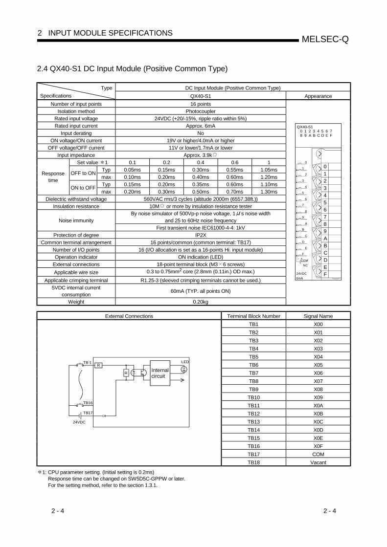
2.4 QX40-S1 DC Input Module (Positive Common Type)
DC Input Module (Positive Common Type) Type Specifications QX40-S1 Appearance
Number of input points 16 points Isolation method Photocoupler
Rated input voltage 24VDC (+20/-15%, ripple ratio within 5%) Rated input current Approx. 6mA
Input derating No ON voltage/ON current 19V or higher/4.0mA or higher
OFF voltage/OFF current 11V or lower/1.7mA or lower Input impedance Approx. 3.9k
Set value 1 0.1 0.2 0.4 0.6 1 Typ 0.05ms 0.15ms 0.30ms 0.55ms 1.05ms OFF to ON max 0.10ms 0.20ms 0.40ms 0.60ms 1.20ms Typ 0.15ms 0.20ms 0.35ms 0.60ms 1.10ms
Response time
ON to OFF max 0.20ms 0.30ms 0.50ms 0.70ms 1.30ms
Dielectric withstand voltage 560VAC rms/3 cycles (altitude 2000m (6557.38ft.)) Insulation resistance 10M or more by insulation resistance tester
By noise simulator of 500Vp-p noise voltage, 1 s noise width and 25 to 60Hz noise frequency Noise immunity
First transient noise IEC61000-4-4: 1kV Protection of degree IP2X
Common terminal arrangement 16 points/common (common terminal: TB17) Number of I/O points 16 (I/O allocation is set as a 16-points Hi. input module) Operation indicator ON indication (LED)
External connections 18-point terminal block (M3 6 screws) Applicable wire size 0.3 to 0.75mm2 core (2.8mm (0.11in.) OD max.)
Applicable crimping terminal R1.25-3 (sleeved crimping terminals cannot be used.) 5VDC internal current
consumption 60mA (TYP. all points ON)
Weight 0.20kg
0
1
2
3
4
5
6
7
8
9
A
B
C
D
E
F
COM
QX40-S1
NC
24VDC6mA
+-
0 1 2 3 4 5 6 78 9 A B C D E F
0123456789ABCDEF
External Connections Terminal Block Number Signal Name
TB1 X00 TB2 X01 TB3 X02 TB4 X03 TB5 X04 TB6 X05 TB7 X06 TB8 X07 TB9 X08 TB10 X09 TB11 X0A TB12 X0B TB13 X0C TB14 X0D TB15 X0E TB16 X0F TB17 COM
RTB 1 LED
TB17
24VDC
R
TB16
Internalcircuit
TB18 Vacant 1: CPU parameter setting. (Initial setting is 0.2ms)
Response time can be changed on SW5D5C-GPPW or later. For the setting method, refer to the section 1.3.1.

2 - 5 2 - 5
MELSEC-Q 2 INPUT MODULE SPECIFICATIONS
2.5 QX41 DC Input Module (Positive Common Type)
DC Input Module (Positive Common Type) Type Specifications QX41 Appearance
Number of input points 32 points Isolation method Photocoupler
Rated input voltage 24VDC (+20/-15%, ripple ratio within 5%) Rated input current Approx. 4mA
Input derating Refer to the derating chart. ON voltage/ON current 19V or higher/3mA or higher
OFF voltage/OFF current 11V or lower/1.7mA or lower Input impedance Approx. 5.6k
OFF to ON 1ms/5ms/10ms/20ms/70ms or less (CPU parameter setting) 1
Initial setting is 10ms. Response time
ON to OFF 1ms/5ms/10ms/20ms/70ms or less (CPU parameter setting) 1
Initial setting is 10ms. Dielectric withstand voltage 560VAC rms/3 cycles (altitude 2000m (6557.38ft.))
Insulation resistance 10M or more by insulation resistance tester By noise simulator of 500Vp-p noise voltage, 1 s noise width
and 25 to 60Hz noise frequency Noise immunity First transient noise IEC61000-4-4: 1kV
Protection of degree IP2X Common terminal arrangement 32 points/common (common terminal: B01, B02)
Number of I/O points 32 (I/O allocation is set as a 32-points input module) Operation indicator ON indication (LED)
External connections 40-pin connector Applicable wire size 0.3mm2 (For A6CON1 or A6CON4) 2
External wiring connector A6CON1, A6CON2, A6CON3, A6CON4 (optional) Applicable connector/terminal block
conversion module A6TBXY36, A6TBXY54, A6TBX70
5VDC internal current consumption 75mA (TYP. all points ON) Weight 0.15kg
QX41
24VDC4mA
QX41
0 1 2 3 4 5 6 78 9 A B C D E F0 1 2 3 4 5 6 78 9 A B C D E F
Derating Chart Pin-Outs Pin No. Signal No. Pin No. Signal No.
B20 X00 A20 X10 B19 X01 A19 X11 B18 X02 A18 X12 B17 X03 A17 X13 B16 X04 A16 X14 B15 X05 A15 X15 B14 X06 A14 X16 B13 X07 A13 X17
100908070605040
0 10 20 30 40 50 55
ONratio
Ambient temperature
28.8VDC
( )
(%)
C
B12 X08 A12 X18 External Connections B11 X09 A11 X19
B10 X0A A10 X1A B09 X0B A09 X1B B08 X0C A08 X1C B07 X0D A07 X1D B06 X0E A06 X1E B05 X0F A05 X1F B04 Vacant A04 Vacant B03 Vacant A03 Vacant B02 COM A02 Vacant
RB20 LED
B02
24VDC
R
A05
B01
Internalcircuit
A20A19A18A17A16A15A14A13A12A11A10A9A8A7A6A5A4A3A2A1
B20B19B18B17B16B15B14B13B12B11B10B9B8B7B6B5B4B3B2B1
Module front view
B01 COM A01 Vacant 1: For the setting method, refer to the section 1.3.1. 2: When using A6CON2 or A6CON3, refer to Chapter 7.

2 - 6 2 - 6
MELSEC-Q 2 INPUT MODULE SPECIFICATIONS
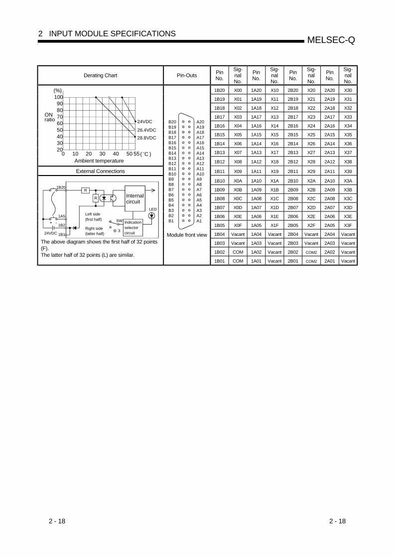
2.6 QX41-S1 DC Input Module (Positive Common Type)
DC Input Module (Positive Common Type) Type Specifications QX41-S1 Appearance
Number of input points 32 points Isolation method Photocoupler
Rated input voltage 24VDC (+20/-15%, ripple ratio within 5%) Rated input current Approx. 4mA
Input derating Refer to the derating chart. ON voltage/ON current 19V or higher/3.0mA or higher
OFF voltage/OFF current 9.5V or lower/1.5mA or lower Input impedance Approx. 5.6k
Set value 1 0.1 0.2 0.4 0.6 1 Typ 0.05ms 0.15ms 0.30ms 0.55ms 1.05ms OFF to ON max 0.12ms 0.20ms 0.40ms 0.60ms 1.20ms Typ 0.15ms 0.20ms 0.35ms 0.60ms 1.10ms
Response time
ON to OFF max 0.20ms 0.30ms 0.50ms 0.70ms 1.30ms
Dielectric withstand voltage 560VAC rms/3 cycles (altitude 2000m (6557.38ft.)) Insulation resistance 10M or more by insulation resistance tester
By noise simulator of 500Vp-p noise voltage, 1 s noise width and 25 to 60Hz noise frequency Noise immunity
First transient noise IEC61000-4-4: 1kV Protection of degree IP2X
Common terminal arrangement 32 points/common (common terminal: B01, B02) Number of I/O points 32 (I/O allocation is set as a 32-points Hi. input module) Operation indicator ON indication (LED)
External connections 40-pin connector Applicable wire size 0.3mm2 (For A6CON1 or A6CON4) 2
External wiring connector A6CON1, A6CON2, A6CON3, A6CON4 (optional) Applicable connector/terminal
block conversion module A6TBXY36, A6TBXY54, A6TBX70
5VDC internal current consumption 75mA (TYP. all points ON)
Weight 0.15kg
QX41-S1
24VDC4mA
QX41-S1
0 1 2 3 4 5 6 78 9 A B C D E F0 1 2 3 4 5 6 78 9 A B C D E F
1: CPU parameter setting. (Initial setting is 0.2ms)
Response time can be changed on SW5D5C-GPPW or later. For the setting method, refer to the section 1.3.1.
2: When using A6CON2 or A6CON3, refer to Chapter 7.

2 - 7 2 - 7
MELSEC-Q 2 INPUT MODULE SPECIFICATIONS
Derating Chart Pin-Outs Pin No. Signal No. Pin No. Signal No.
B20 X00 A20 X10 B19 X01 A19 X11 B18 X02 A18 X12 B17 X03 A17 X13 B16 X04 A16 X14 B15 X05 A15 X15 B14 X06 A14 X16 B13 X07 A13 X17
100908070605040
0 10 20 30 40 50 55
ONratio
Ambient temperature
28.8VDC
( )
(%)
C
B12 X08 A12 X18 External Connections B11 X09 A11 X19
B10 X0A A10 X1A B09 X0B A09 X1B B08 X0C A08 X1C B07 X0D A07 X1D B06 X0E A06 X1E B05 X0F A05 X1F B04 Vacant A04 Vacant B03 Vacant A03 Vacant B02 COM A02 Vacant
RB20 LED
B02
24VDC
R
A05
B01
Internalcircuit
A20A19A18A17A16A15A14A13A12A11A10A9A8A7A6A5A4A3A2A1
B20B19B18B17B16B15B14B13B12B11B10B9B8B7B6B5B4B3B2B1
Module front view
B01 COM A01 Vacant

2 - 8 2 - 8
MELSEC-Q 2 INPUT MODULE SPECIFICATIONS
2.7 QX42 DC Input Module (Positive Common Type)
DC Input Module (Positive Common Type) Type Specifications QX42 Appearance
Number of input points 64 points Isolation method Photocoupler
Rated input voltage 24VDC (+20/-15%, ripple ratio within 5%) Rated input current Approx. 4mA
Input derating Refer to the derating chart. ON voltage/ON current 19V or higher/3mA or higher
OFF voltage/OFF current 11V or lower/1.7mA or lower Input impedance Approx. 5.6k
OFF to ON 1ms/5ms/10ms/20ms/70ms or less (CPU parameter setting) 1 Initial setting is 10ms. Response
time ON to OFF 1ms/5ms/10ms/20ms/70ms or less (CPU parameter setting) 1 Initial setting is 10ms.
Dielectric withstand voltage 560VAC rms/3 cycles (altitude 2000m (6557.38ft.)) Insulation resistance 10M or more by insulation resistance tester
By noise simulator of 500Vp-p noise voltage, 1 s noise width and 25 to 60Hz noise frequency Noise immunity
First transient noise IEC61000-4-4: 1kV Protection of degree IP2X
Common terminal arrangement 32 points/common (common terminal: 1B01, 1B02, 2B01, 2B02) Number of I/O points 64 (I/O allocation is set as a 32-points input module) Operation indicator ON indication (LED), 32 point switch-over using switch
External connections 40-pin connector Applicable wire size 0.3mm2 (For A6CON1 or A6CON4) 4
External wiring connector A6CON1, A6CON2, A6CON3, A6CON4 (optional) Applicable connector/terminal block
conversion module A6TBXY36, A6TBXY54, A6TBX70
5VDC internal current consumption 90mA (TYP. all points ON) Weight 0.18kg
QX42
24VDC4mA
QX42DISPLAY
F L
0 1 2 3 4 5 6 78 9 A B C D E F0 1 2 3 4 5 6 78 9 A B C D E F
Derating Chart Pin-Outs Pin No.
Sig-nal No.
Pin No.
Sig-nal No.
Pin No.
Sig-nal No.
Pin No.
Sig-nal No.
1B20 X00 1A20 X10 2B20 X20 2A20 X30
1B19 X01 1A19 X11 2B19 X21 2A19 X31
1B18 X02 1A18 X12 2B18 X22 2A18 X32
1B17 X03 1A17 X13 2B17 X23 2A17 X33
1B16 X04 1A16 X14 2B16 X24 2A16 X34
1B15 X05 1A15 X15 2B15 X25 2A15 X35
1B14 X06 1A14 X16 2B14 X26 2A14 X36
1B13 X07 1A13 X17 2B13 X27 2A13 X37
100908070605040
0 10 20 30 40 50 55
ONratio
Ambient temperature
24VDC
3020
26.4VDC28.8VDC
( )
(%)
C 1B12 X08 1A12 X18 2B12 X28 2A12 X38
External Connections 1B11 X09 1A11 X19 2B11 X29 2A11 X39
1B10 X0A 1A10 X1A 2B10 X2A 2A10 X3A
1B09 X0B 1A09 X1B 2B09 X2B 2A09 X3B
1B08 X0C 1A08 X1C 2B08 X2C 2A08 X3C
1B07 X0D 1A07 X1D 2B07 X2D 2A07 X3D
1B06 X0E 1A06 X1E 2B06 X2E 2A06 X3E
1B05 X0F 1A05 X1F 2B05 X2F 2A05 X3F
1B04 Vacant 1A04 Vacant 2B04 Vacant 2A04 Vacant
1B03 Vacant 1A03 Vacant 2B03 Vacant 2A03 Vacant
1B02 COM 1A02 Vacant 2B02 COM2 2A02 Vacant
R
R1B20
1B2
1B1
LED
SW+-1A5 Left side
(first half)
24VDC 3Right side(latter half)
Indicationselectorcircuit
Internalcircuit
The above diagram shows the first half of 32 points (F). The latter half of 32 points (L) are similar.
A20A19A18A17A16A15A14A13A12A11A10A9A8A7A6A5A4A3A2A1
B20B19B18B17B16B15B14B13B12B11B10B9B8B7B6B5B4B3B2B1
Module front view
1B01 COM 1A01 Vacant 2B01 COM2 2A01 Vacant
1: For the setting method, refer to the section 1.3.1. 2: Pin number of 1 indicates that of the left-hand side connector, and pin number of 2 indicates that of the right-hand
side connector. 3: Selection of left-hand (F) side provides the first half (X00 to X1F) LED indications, and selection of right-hand (L) side provides the
latter half (X20 to X3F) LED indications. 4: When using A6CON2 or A6CON3, refer to Chapter 7.

2 - 9 2 - 9
MELSEC-Q 2 INPUT MODULE SPECIFICATIONS
2.8 QX42-S1 DC Input Module (Positive Common Type)
DC Input Module (Positive Common Type) Type Specifications QX42-S1 Appearance
Number of input points 64 points Isolation method Photocoupler
Rated input voltage 24VDC (+20/-15%, ripple ratio within 5%) Rated input current Approx. 4mA
Input derating Refer to the derating chart. ON voltage/ON current 19V or higher/3.0mA or higher
OFF voltage/OFF current 9.5V or lower/1.5mA or lower Input impedance Approx. 5.6k
Set value 1 0.1 0.2 0.4 0.6 1 Typ 0.05ms 0.15ms 0.30ms 0.55ms 1.05ms OFF to ON max 0.12ms 0.20ms 0.40ms 0.60ms 1.20ms Typ 0.15ms 0.20ms 0.35ms 0.60ms 1.10ms
Response time
ON to OFF max 0.20ms 0.30ms 0.50ms 0.70ms 1.30ms
Dielectric withstand voltage 560VAC rms/3 cycles (altitude 2000m (6557.38ft.)) Insulation resistance 10M or more by insulation resistance tester
By noise simulator of 500Vp-p noise voltage, 1 s noise width and 25 to 60Hz noise frequency Noise immunity
First transient noise IEC61000-4-4: 1kV Protection of degree IP2X
Common terminal arrangement 32 points/common (common terminal: 1B01, 1B02, 2B01, 2B02) Number of I/O points 64 (I/O allocation is set as a 64-points Hi. input module) Operation indicator ON indication (LED)
External connections 40-pin connector Applicable wire size 0.3mm2 (For A6CON1 or A6CON4) 4
External wiring connector A6CON1, A6CON2, A6CON3, A6CON4 (optional) Applicable connector/terminal
block conversion module A6TBXY36, A6TBXY54, A6TBX70
5VDC internal current consumption 90mA (TYP. all points ON)
Weight 0.18kg
QX42-S1
24VDC4mA
QX42-S1DISPLAY
F L
0 1 2 3 4 5 6 78 9 A B C D E F0 1 2 3 4 5 6 78 9 A B C D E F
1: CPU parameter setting. (Initial setting is 0.2ms)
Response time can be changed on SW5D5C-GPPW or later. For the setting method, refer to the section 1.3.1.
2: Pin number of 1 indicates that of the left-hand side connector, and pin number of 2 indicates that of the right-hand side connector.
3: Selection of left-hand (F) side provides the first half (X00 to X1F) LED indications, and selection of right-hand (L) side provides the latter half (X20 to X3F) LED indications.
4: When using A6CON2 or A6CON3, refer to Chapter 7.

2 - 10 2 - 10
MELSEC-Q 2 INPUT MODULE SPECIFICATIONS
Derating Chart Pin-Outs Pin No.
Sig-nal No.
Pin No.
Sig-nal No.
Pin No.
Sig-nal No.
Pin No.
Sig-nal No.
1B20 X00 1A20 X10 2B20 X20 2A20 X30
1B19 X01 1A19 X11 2B19 X21 2A19 X31
1B18 X02 1A18 X12 2B18 X22 2A18 X32
1B17 X03 1A17 X13 2B17 X23 2A17 X33
1B16 X04 1A16 X14 2B16 X24 2A16 X34
1B15 X05 1A15 X15 2B15 X25 2A15 X35
1B14 X06 1A14 X16 2B14 X26 2A14 X36
1B13 X07 1A13 X17 2B13 X27 2A13 X37
100908070605040
0 10 20 30 40 50 55
ONratio
Ambient temperature
24VDC
3020
26.4VDC28.8VDC
( )
(%)
C 1B12 X08 1A12 X18 2B12 X28 2A12 X38
External Connections 1B11 X09 1A11 X19 2B11 X29 2A11 X39
1B10 X0A 1A10 X1A 2B10 X2A 2A10 X3A
1B09 X0B 1A09 X1B 2B09 X2B 2A09 X3B
1B08 X0C 1A08 X1C 2B08 X2C 2A08 X3C
1B07 X0D 1A07 X1D 2B07 X2D 2A07 X3D
1B06 X0E 1A06 X1E 2B06 X2E 2A06 X3E
1B05 X0F 1A05 X1F 2B05 X2F 2A05 X3F
1B04 Vacant 1A04 Vacant 2B04 Vacant 2A04 Vacant
1B03 Vacant 1A03 Vacant 2B03 Vacant 2A03 Vacant
1B02 COM 1A02 Vacant 2B02 COM2 2A02 Vacant
R
R1B20
1B2
1B1
LED
SW+-1A5 Left side
(first half)
24VDC 3Right side(latter half)
Indicationselectorcircuit
Internalcircuit
The above diagram shows the first half of 32 points (F). The latter half of 32 points (L) are similar.
A20A19A18A17A16A15A14A13A12A11A10A9A8A7A6A5A4A3A2A1
B20B19B18B17B16B15B14B13B12B11B10B9B8B7B6B5B4B3B2B1
Module front view
1B01 COM 1A01 Vacant 2B01 COM2 2A01 Vacant

2 - 11 2 - 11
MELSEC-Q 2 INPUT MODULE SPECIFICATIONS
2.9 QX70 DC Input Module (Positive Common/Negative Common Shared Type)
DC Input Module (Positive Common/Negative Common Shared Type) Type Specifications QX70 Appearance
Number of input points 16 points Insulation method Photocoupler
Rated input voltage 5VDC
(+20/-15%, ripple ratio within 5%) 12VDC
(+20/-15%, ripple ratio within 5%) Rated input current Approx. 1.2mA Approx. 3.3mA
Input derating None ON voltage/ON current 3.5V or higher/1mA or higher
OFF voltage/OFF current 1V or lower/0.1mA or lower Input resistance Approx. 3.3k
OFF ON 1ms/5ms/10ms/20ms/70ms or less (CPU parameter setting)
Initial setting is 10ms Response time
ON OFF 1ms/5ms/10ms/20ms/70ms or less (CPU parameter setting)
Initial setting is 10ms Dielectric maximum voltage 560VAC rms/3 cycles (altitude 2000m)
Insulation resistance 10M or more by insulation resistance tester By noise simulator of 500Vp-p noise voltage,
1 s noise width and 25 to 60Hz noise frequency Noise immunity First transient noise IEC61000-4-4: 0.25kV
Protection of degree IP2X Common terminal arrangement 16 points/common (common terminal: TB17)
Number of I/O points 16 (I/O allocation is set as a 16-points input module) Operation indicator ON indication (LED)
External connections 18-point terminal block (M3 6 screw) Applicable wire size Core cable: 0.3 to 0.75mm2 (Outside diameter: 2.8mm or smaller)
Applicable connector terminal R1.25-3 (Terminals with sleeve cannot be used) 5VDC internal current
consumption 55mA (TYP, all points ON)
Weight 0.14kg
0
1
2
3
4
5
6
7
8
9
A
B
C
D
E
F
COM
QX70
NC
+-
0 1 2 3 4 5 6 78 9 A B C D E F
0123456789ABCDEF
5/12VDC1.2mA3.3mA
External Connections Terminal Block No. Signal Name
TB1 X00 TB2 X01 TB3 X02 TB4 X03 TB5 X04 TB6 X05 TB7 X06 TB8 X07 TB9 X08 TB10 X09 TB11 X0A TB12 X0B TB13 X0C TB14 X0D TB15 X0E TB16 X0F TB17 COM
R
TB 1
TB17
5/12VDC
LEDR
For open collector (positive common) connection
For TTL, LS-TTL, CMOS buffer (positive common) connections
TB17
TB 1
For sensor (negative common) connections
TB17
TB 1
Internalcircuit
TB18 Vacant : For the setting method, refer to the section 1.3.1.

2 - 12 2 - 12
MELSEC-Q 2 INPUT MODULE SPECIFICATIONS
2.10 QX71 DC Input Module (Positive Common/Negative Common Shared Type)
DC Input Module (Positive Common/Negative Common Shared Type) Type Specifications QX71 Appearance
Number of input points 32 points Insulation method Photocoupler
Rated input voltage 5VDC (+20/-15%, ripple ratio within 5%)
12VDC (+20/-15%, ripple ratio within 5%)
Rated input current Approx. 1.2mA Approx. 3.3mA Input derating None
ON voltage/ON current 3.5V or higher/1mA or higher OFF voltage/OFF current 1V or lower/0.1mA or lower
Input resistance Approx. 3.3k
OFF ON 1ms/5ms/10ms/20ms/70ms or less (CPU parameter setting) 1
Initial setting is 10ms Response time
ON OFF 1ms/5ms/10ms/20ms/70ms or less (CPU parameter setting) 1
Initial setting is 10ms Dielectric maximum voltage 560VAC rms/3 cycles (altitude 2000m)
Insulation resistance 10M or more by insulation resistance tester By noise simulator of 500Vp-p noise voltage,
1 s noise width and 25 to 60Hz noise frequency Noise immunity First transient noise IEC61000-4-4: 0.25kV
Protection of degree IP2X Common terminal arrangement 32 points/common (common terminal: B01, B02)
Number of I/O points 32 (I/O allocation is set as a 32-points input module) Operation indicator ON indication (LED)
External connections 40-pin connector Applicable wire size 0.3mm2 (For A6CON1 or A6CON4) 2
External wiring connector A6CON1, A6CON2, A6CON3, A6CON4 (optional) 5VDC internal current
consumption 70mA (TYP, all points ON)
Weight 0.12kg
QX71
5/12VDC1.2 / 3.3mA
QX71
0 1 2 3 4 5 6 78 9 A B C D E F0 1 2 3 4 5 6 78 9 A B C D E F
External Connections Pin-Outs Pin No. Signal
No. Pin No. Signal No.
B20 X00 A20 X10 B19 X01 A19 X11 B18 X02 A18 X12 B17 X03 A17 X13 B16 X04 A16 X14 B15 X05 A15 X15 B14 X06 A14 X16 B13 X07 A13 X17 B12 X08 A12 X18 B11 X09 A11 X19 B10 X0A A10 X1A B09 X0B A09 X1B B08 X0C A08 X1C B07 X0D A07 X1D B06 X0E A06 X1E B05 X0F A05 X1F B04 Vacant A04 Vacant B03 Vacant A03 Vacant B02 COM A02 Vacant
R
B20
B02
5/12VDC
LEDR
For open collector (positive common) connection
For TTL, LS-TTL, CMOS buffer (positive common) connections
B02
B20
For sensor (negative common) connections
B02
B20
B01
Internalcircuit
A20A19A18A17A16A15A14A13A12A11A10A9A8A7A6A5A4A3A2A1
B20B19B18B17B16B15B14B13B12B11B10B9B8B7B6B5B4B3B2B1
Module front view B01 COM A01 Vacant
1: For the setting method, refer to the section 1.3.1. 2: When using A6CON2 or A6CON3, refer to Chapter 7.

2 - 13 2 - 13
MELSEC-Q 2 INPUT MODULE SPECIFICATIONS
2.11 QX72 DC Input Module (Positive Common/Negative Common Shared Type)
DC Input Module (Positive Common/Negative Common Shared Type) Type Specifications QX72 Appearance
Number of input points 64 points Insulation method Photocoupler
Rated input voltage 5VDC
(+20/-15%, ripple ratio within 5%)
12VDC (+20/-15%, ripple ratio within 5%)
Rated input current Approx. 1.2mA Approx. 3.3mA Input derating None
ON voltage/ON current 3.5V or higher/3mA or higher OFF voltage/OFF current 1V or lower/0.1mA or lower
Input resistance Approx. 3.3k
OFF ON 1ms/5ms/10ms/20ms/70ms or less (CPU parameter setting) 1 Initial setting is 10ms Response
time ON OFF 1ms/5ms/10ms/20ms/70ms or less (CPU parameter setting) 1
Initial setting is 10ms Dielectric maximum voltage 560VAC rms/3 cycles (altitude 2000m)
Insulation resistance 10M or more by insulation resistance tester By noise simulator of 500Vp-p noise voltage,
1 s noise width and 25 to 60Hz noise frequency Noise immunity First transient noise IEC61000-4-4: 0.25kV
Protection of degree IP2X Common terminal arrangement 32 points/common (common terminal: 1B01, 1B02, 2B01, 2B02)
Number of I/O points 64 (I/O allocation is set as a 64-points input module) Operation indicator ON indication (LED), 32-point switchover using switch
External connections 40-pin connector Applicable wire size 0.3mm2 (For A6CON1 or A6CON4) 4
External wiring connector A6CON1, A6CON2, A6CON3, A6CON4 (optional) 5VDC internal current consumption 85mA (TYP, all points ON)
Weight 0.13kg
QX72
QX72DISPLAY
F L
0 1 2 3 4 5 6 78 9 A B C D E F0 1 2 3 4 5 6 78 9 A B C D E F
5/12VDC1.2/3.3mA
External Connections Pin-Outs Pin No. Signal
No. Pin No. Signal No. Pin No. Signal
No. Pin No. Signal No.
1B20 X00 1A20 X10 2B20 X20 2A20 X30 1B19 X01 1A19 X11 2B19 X21 2A19 X31 1B18 X02 1A18 X12 2B18 X22 2A18 X32 1B17 X03 1A17 X13 2B17 X23 2A17 X33 1B16 X04 1A16 X14 2B16 X24 2A16 X34 1B15 X05 1A15 X15 2B15 X25 2A15 X35 1B14 X06 1A14 X16 2B14 X26 2A14 X36 1B13 X07 1A13 X17 2B13 X27 2A13 X37 1B12 X08 1A12 X18 2B12 X28 2A12 X38 1B11 X09 1A11 X19 2B11 X29 2A11 X39 1B10 X0A 1A10 X1A 2B10 X2A 2A10 X3A 1B09 X0B 1A09 X1B 2B09 X2B 2A09 X3B 1B08 X0C 1A08 X1C 2B08 X2C 2A08 X3C 1B07 X0D 1A07 X1D 2B07 X2D 2A07 X3D 1B06 X0E 1A06 X1E 2B06 X2E 2A06 X3E 1B05 X0F 1A05 X1F 2B05 X2F 2A05 X3F 1B04 Vacant 1A04 Vacant 2B04 Vacant 2A04 Vacant 1B03 Vacant 1A03 Vacant 2B03 Vacant 2A03 Vacant 1B02 COM1 1A02 Vacant 2B02 COM2 2A02 Vacant
R
1B20
1B02
5/12VDC
LEDR
For open collector (positive common) connection
For TTL, LS-TTL, CMOS buffer (positive common) connections
1B02
1B20
For sensor (negative common) connections
1B02
1B20
1B01
LEDSWLeft side (first half)Right side (latter half)
3Indicationselectorcircuit
Internalcircuit
The above diagram shows the first half of 32 points (F). The latter half of 32 points (L) are similar.
A20A19A18A17A16A15A14A13A12A11A10A9A8A7A6A5A4A3A2A1
B20B19B18B17B16B15B14B13B12B11B10B9B8B7B6B5B4B3B2B1
Module front view
1B01 COM1 1A01 Vacant 2B01 COM2 2A01 Vacant 1: For the setting method, refer to the section 1.3.1. 2: Pin number of 1 indicates that of the left-hand side connector, and pin number of 2 indicates that of the right-hand
side connector. 3: Selection of left-hand (F) side provides the first half (X00 to X1F) LED indications, and selection of right-hand (L) side provides the
latter half (X20 to X3F) LED indications. 4: When using A6CON2 or A6CON3, refer to Chapter 7.

2 - 14 2 - 14
MELSEC-Q 2 INPUT MODULE SPECIFICATIONS
2.12 QX80 DC Input Module (Negative Common Type)
DC Input Module (Negative Common Type) Type Specifications QX80 Appearance
Number of input points 16 points Isolation method Photocoupler
Rated input voltage 24VDC (+20/-15%, ripple ratio within 5%) Rated input current Approx. 4mA
Input derating No ON voltage/ON current 19V or higher/3mA or higher
OFF voltage/OFF current 11V or lower/1.7mA or lower Input impedance Approx. 5.6k
OFF to ON 1ms/5ms/10ms/20ms/70ms or less (CPU parameter setting)
Initial setting is 10ms. Response time
ON to OFF 1ms/5ms/10ms/20ms/70ms or less (CPU parameter setting)
Initial setting is 10ms. Dielectric withstand voltage 560VAC rms/3 cycles (altitude 2000m (6557.38ft.))
Insulation resistance 10M or more by insulation resistance tester By noise simulator of 500Vp-p noise voltage, 1 s noise width
and 25 to 60Hz noise frequency Noise immunity First transient noise IEC61000-4-4: 1kV
Protection of degree IP2X Common terminal arrangement 16 points/common (common terminal: TB18)
Number of I/O points 16 (I/O allocation is set as a 16-points input module) Operation indicator ON indication (LED)
External connections 18-point terminal block (M3 6 screws) Applicable wire size 0.3 to 0.75mm2 core (2.8mm (0.11in.) OD max.)
Applicable crimping terminal R1.25-3 (sleeved crimping terminals cannot be used.) 5VDC internal current consumption 50mA (TYP. all points ON)
Weight 0.16kg
0
1
2
3
4
5
6
7
8
9
A
B
C
D
E
F
COM
QX80
NC
24VDC4mA
0 1 2 3 4 5 6 78 9 A B C D E F
0123456789ABCDEF
External Connections Terminal Block Number Signal Name
TB1 X00 TB2 X01 TB3 X02 TB4 X03 TB5 X04 TB6 X05 TB7 X06 TB8 X07 TB9 X08 TB10 X09 TB11 X0A TB12 X0B TB13 X0C TB14 X0D TB15 X0E TB16 X0F TB17 Vacant
RTB 1 LED
TB18
24VDC
R
TB16
Internalcircuit
TB18 COM : For the setting method, refer to the section 1.3.1.

2 - 15 2 - 15
MELSEC-Q 2 INPUT MODULE SPECIFICATIONS
2.13 QX81 DC Input Module (Negative Common Type)
DC Input Module (Negative Common Type) Type Specifications QX81 Appearance
Number of input points 32 points Isolation method Photocoupler
Rated input voltage 24VDC (+20/-15%, ripple ratio within 5%) Rated input current Approx. 4mA
Input derating Refer to the derating chart. ON voltage/ON current 19V or higher/3mA or higher
OFF voltage/OFF current 11V or lower/1.7mA or lower Input impedance Approx. 5.6k
OFF to ON 1ms/5ms/10ms/20ms/70ms or less (CPU parameter setting) 1 Initial setting is 10ms. Response
time ON to OFF 1ms/5ms/10ms/20ms/70ms or less (CPU parameter setting) 1
Initial setting is 10ms. Dielectric withstand voltage 560VAC rms/3 cycles (altitude 2000m (6557.38ft.))
Insulation resistance 10M or more by insulation resistance tester By noise simulator of 500Vp-p noise voltage, 1 s noise width
and 25 to 60Hz noise frequency Noise immunity First transient noise IEC61000-4-4: 1kV
Protection of degree IP2X Common terminal arrangement 32 points/common (common terminal: 17, 18, 36)
Number of I/O points 32 (I/O allocation is set as a 32-points input module) Operation indicator ON indication (LED)
External connections 37-pin D-sub connector Applicable wire size 0.3mm2 (For A6CON1E) 2
External wiring connector A6CON1E, A6CON2E, A6CON3E (optional) Applicable connector/terminal block
conversion module A6TBX36-E, A6TBX54-E, A6TBX70-E
5VDC internal current consumption 75mA (TYP. all points ON) Weight 0.16kg
QX81
24VDC4mA
QX81
0 1 2 3 4 5 6 78 9 A B C D E F0 1 2 3 4 5 6 78 9 A B C D E F
Derating Chart Pin-Outs Pin No. Signal No. Pin No. Signal No.
1 X00 9 X10 20 X01 28 X11 2 X02 10 X12 21 X03 29 X13 3 X04 11 X14 22 X05 30 X15 4 X06 12 X16 23 X07 31 X17
100908070605040
0 10 20 30 40 50 55
ONratio 28.8VDC
(%)
( )CAmbient temperature
5 X08 13 X18 External Connections 24 X09 32 X19
6 X0A 14 X1A 25 X0B 33 X1B 7 X0C 15 X1C 26 X0D 34 X1D 8 X0E 16 X1E 27 X0F 35 X1F 17 COM 37 Vacant 36 COM 19 Vacant R
LED
24VDC
R
183617
35
1Internalcircuit
373635343332313029282726252423222120
19181716151413121110987654321
Module front view
18 COM 1: For the setting method, refer to the section 1.3.1. 2: When using A6CON2E or A6CON3E, refer to Chapter 7.

2 - 16 2 - 16
MELSEC-Q 2 INPUT MODULE SPECIFICATIONS
2.14 QX82 DC Input Module (Negative Common Type)
DC Input Module (Negative Common Type) Type Specifications QX82 Appearance
Number of input points 64 points Isolation method Photocoupler
Rated input voltage 24VDC (+20/-15%, ripple ratio within 5%) Rated input current Approx. 4mA
Input derating Refer to the derating chart. ON voltage/ON current 19V or higher/3mA or higher
OFF voltage/OFF current 11V or lower/1.7mA or lower Input impedance Approx. 5.6k
OFF to ON 1ms/5ms/10ms/20ms/70ms or less (CPU parameter setting) 1 Initial setting is 10ms. Response
time ON to OFF 1ms/5ms/10ms/20ms/70ms or less (CPU parameter setting) 1 Initial setting is 10ms.
Dielectric withstand voltage 560VAC rms/3 cycles (altitude 2000m (6557.38ft.)) Insulation resistance 10M or more by insulation resistance tester
By noise simulator of 500Vp-p noise voltage, 1 s noise width and 25 to 60Hz noise frequency Noise immunity
First transient noise IEC61000-4-4: 1kV Protection of degree IP2X
Common terminal arrangement 32 points/common (common terminal: 1B01, 1B02, 2B01, 2B02) Number of I/O points 64 (I/O allocation is set as a 32-points input module) Operation indicator ON indication (LED), 32 point switch-over using switch
External connections 40-pin connector Applicable wire size 0.3mm2 (For A6CON1 or A6CON4) 4
External wiring connector A6CON1, A6CON2, A6CON3, A6CON4 (optional) Applicable connector/terminal block
conversion module —————
5VDC internal current consumption 90mA (TYP. all points ON) Weight 0.18kg
QX82
24VDC4mA
QX82DISPLAY
F L
0 1 2 3 4 5 6 78 9 A B C D E F0 1 2 3 4 5 6 78 9 A B C D E F
Derating Chart Pin-Outs Pin No.
Sig-nal No.
Pin No.
Sig-nal No.
Pin No.
Sig-nal No.
Pin No.
Sig-nal No.
1B20 X00 1A20 X10 2B20 X20 2A20 X30
1B19 X01 1A19 X11 2B19 X21 2A19 X31
1B18 X02 1A18 X12 2B18 X22 2A18 X32
1B17 X03 1A17 X13 2B17 X23 2A17 X33
1B16 X04 1A16 X14 2B16 X24 2A16 X34
1B15 X05 1A15 X15 2B15 X25 2A15 X35
1B14 X06 1A14 X16 2B14 X26 2A14 X36
1B13 X07 1A13 X17 2B13 X27 2A13 X37
100908070605040
0 10 20 30 40 50 55
ONratio
Ambient temperature
24VDC
3020
26.4VDC28.8VDC
( )
(%)
C 1B12 X08 1A12 X18 2B12 X28 2A12 X38
External Connections 1B11 X09 1A11 X19 2B11 X29 2A11 X39
1B10 X0A 1A10 X1A 2B10 X2A 2A10 X3A
1B09 X0B 1A09 X1B 2B09 X2B 2A09 X3B
1B08 X0C 1A08 X1C 2B08 X2C 2A08 X3C
1B07 X0D 1A07 X1D 2B07 X2D 2A07 X3D
1B06 X0E 1A06 X1E 2B06 X2E 2A06 X3E
1B05 X0F 1A05 X1F 2B05 X2F 2A05 X3F
1B04 Vacant 1A04 Vacant 2B04 Vacant 2A04 Vacant
1B03 Vacant 1A03 Vacant 2B03 Vacant 2A03 Vacant
1B02 COM 1A02 Vacant 2B02 COM2 2A02 Vacant
R
R1B20
1B2
1B1
LED
SW1A5 Left side
(first half)
24VDC 3Right side(latter half)
Indicationselectorcircuit
Internalcircuit
The above diagram shows the first half of 32 points (F). The latter half of 32 points (L) are similar.
A20A19A18A17A16A15A14A13A12A11A10A9A8A7A6A5A4A3A2A1
B20B19B18B17B16B15B14B13B12B11B10B9B8B7B6B5B4B3B2B1
Module front view
1B01 COM 1A01 Vacant 2B01 COM2 2A01 Vacant
1: For the setting method, refer to the section 1.3.1. 2: Pin number of 1 indicates that of the left-hand side connector, and pin number of 2 indicates that of the right-hand
side connector. 3: Selection of left-hand (F) side provides the first half (X00 to X1F) LED indications, and selection of right-hand (L) side provides the
latter half (X20 to X3F) LED indications. 4: When using A6CON2 or A6CON3, refer to Chapter 7.

2 - 17 2 - 17
MELSEC-Q 2 INPUT MODULE SPECIFICATIONS
2.15 QX82-S1 DC Input Module (Negative Common Type)
DC Input Module (Negative Common Type) Type Specifications QX82-S1 Appearance
Number of input points 64 points Isolation method Photocoupler
Rated input voltage 24VDC (+20/-15%, ripple ratio within 5%) Rated input current Approx. 4mA
Input derating Refer to the derating chart. ON voltage/ON current 19V or higher/3.0mA or higher
OFF voltage/OFF current 9.5V or lower/1.5mA or lower Input impedance Approx. 5.6k
Set value 1 0.1 0.2 0.4 0.6 1 Typ 0.05ms 0.15ms 0.30ms 0.55ms 1.05ms OFF to ON max 0.12ms 0.20ms 0.40ms 0.60ms 1.20ms Typ 0.15ms 0.20ms 0.35ms 0.60ms 1.10ms
Response time
ON to OFF max 0.20ms 0.30ms 0.50ms 0.70ms 1.30ms
Dielectric withstand voltage 560VAC rms/3 cycles (altitude 2000m (6557.38ft.)) Insulation resistance 10M or more by insulation resistance tester
By noise simulator of 500Vp-p noise voltage, 1 s noise width and 25 to 60Hz noise frequency Noise immunity
First transient noise IEC61000-4-4: 1kV Protection of degree IP2X
Common terminal arrangement 32 points/common (common terminal: 1B01, 1B02, 2B01, 2B02) Number of I/O points 64 (I/O allocation is set as a 64-points Hi. input module) Operation indicator ON indication (LED)
External connections 40-pin connector Applicable wire size 0.3mm2 (For A6CON1 or A6CON4) 4
External wiring connector A6CON1, A6CON2, A6CON3, A6CON4 (optional) Applicable connector/terminal
block conversion module —————
5VDC internal current consumption 90mA (TYP. all points ON)
Weight 0.18kg
QX82-S1
24VDC4mA
QX82-S1DISPLAY
F L
0 1 2 3 4 5 6 78 9 A B C D E F0 1 2 3 4 5 6 78 9 A B C D E F
1: CPU parameter setting. (Initial setting is 0.2ms)
Response time can be changed on SW5D5C-GPPW or later. For the setting method, refer to the section 1.3.1.
2: Pin number of 1 indicates that of the left-hand side connector, and pin number of 2 indicates that of the right-hand side connector.
3: Selection of left-hand (F) side provides the first half (X00 to X1F) LED indications, and selection of right-hand (L) side provides the latter half (X20 to X3F) LED indications.
4: When using A6CON2 or A6CON3, refer to Chapter 7.
2 - 18 2 - 18
MELSEC-Q 2 INPUT MODULE SPECIFICATIONS
Derating Chart Pin-Outs Pin No.
Sig-nal No.
Pin No.
Sig-nal No.
Pin No.
Sig-nal No.
Pin No.
Sig-nal No.
1B20 X00 1A20 X10 2B20 X20 2A20 X30
1B19 X01 1A19 X11 2B19 X21 2A19 X31
1B18 X02 1A18 X12 2B18 X22 2A18 X32
1B17 X03 1A17 X13 2B17 X23 2A17 X33
1B16 X04 1A16 X14 2B16 X24 2A16 X34
1B15 X05 1A15 X15 2B15 X25 2A15 X35
1B14 X06 1A14 X16 2B14 X26 2A14 X36
1B13 X07 1A13 X17 2B13 X27 2A13 X37
100908070605040
0 10 20 30 40 50 55
ONratio
Ambient temperature
24VDC
3020
26.4VDC28.8VDC
( )
(%)
C 1B12 X08 1A12 X18 2B12 X28 2A12 X38
External Connections 1B11 X09 1A11 X19 2B11 X29 2A11 X39
1B10 X0A 1A10 X1A 2B10 X2A 2A10 X3A
1B09 X0B 1A09 X1B 2B09 X2B 2A09 X3B
1B08 X0C 1A08 X1C 2B08 X2C 2A08 X3C
1B07 X0D 1A07 X1D 2B07 X2D 2A07 X3D
1B06 X0E 1A06 X1E 2B06 X2E 2A06 X3E
1B05 X0F 1A05 X1F 2B05 X2F 2A05 X3F
1B04 Vacant 1A04 Vacant 2B04 Vacant 2A04 Vacant
1B03 Vacant 1A03 Vacant 2B03 Vacant 2A03 Vacant
1B02 COM 1A02 Vacant 2B02 COM2 2A02 Vacant
R
R1B20
1B2
1B1
LED
SW1A5 Left side
(first half)
24VDC 3Right side(latter half)
Indicationselectorcircuit
Internalcircuit
The above diagram shows the first half of 32 points (F). The latter half of 32 points (L) are similar.
A20A19A18A17A16A15A14A13A12A11A10A9A8A7A6A5A4A3A2A1
B20B19B18B17B16B15B14B13B12B11B10B9B8B7B6B5B4B3B2B1
Module front view
1B01 COM 1A01 Vacant 2B01 COM2 2A01 Vacant

3 - 1 3 - 1
MELSEC-Q 3 OUTPUT MODULE SPECIFICATIONS
3. OUTPUT MODULE SPECIFICATIONS
3.1 QY10 Contact Output Module
Contact Output Module Type Specifications QY10 Appearance
Number of output points 16 points Isolation method Relay
Rated switching voltage, current
24VDC 2A (resistive load) 240VAC 2A (cos =1) /point, 8A/common
Minimum switching load 5VDC 1mA Maximum switching load 264VAC 125VDC
OFF to ON 10ms or less Response time ON to OFF 12ms or less
Mechanical 20 million times or more Rated switching voltage/current load
More than 100 thousand times or more 200VAC 1.5A, 240VAC 1A (COS =0.7) 100 thousand times or more
200VAC 0.4A, 240VAC 0.3A (COS =0.7) 300 thousand times or more 200VAC 1A, 240VAC 0.5A (COS =0.35) 100 thousand times or more
200VAC 0.3A, 240VAC 0.15A (COS =0.35) 300 thousand times or more
Life Electrical
24VDC 1A, 100VDC 0.1A (L/R=7ms) 100 thousand times or more 24VDC 0.3A, 100VDC 0.03A (L/R=7ms) 300 thousand times or more
Maximum switching frequency 3600 times/hour
Surge suppressor No Fuse No
Dielectric withstand voltage 2830VAC rms/3 cycles (altitude 2000m (6557.38ft.)) Insulation resistance 10M or more by insulation resistance tester
By noise simulator of 1500Vp-p noise voltage, 1 s noise width and 25 to 60Hz noise frequency Noise immunity
First transient noise IEC61000-4-4: 1kV Protection of degree IP1X Common terminal
arrangement 16 points/common (common terminal: TB17)
Number of I/O points 16 (I/O allocation is set as a 16-points output module) Operation indicator ON indication (LED)
External connections 18-point terminal block (M3 6 screws) Applicable wire size 0.3 to 0.75mm2 core (2.8mm (0.11in.) OD max.)
Applicable crimping terminal R1.25-3 (sleeved crimping terminals cannot be used.) 5VDC internal current
consumption 430mA (TYP. all points ON)
Weight 0.22kg
0
1
2
3
4
5
6
7
8
9
A
B
C
D
E
F
COM
QY10
NC24VDC240VAC2A
L
L
L
L
L
L
L
L
L
L
L
L
L
L
L
L
0 1 2 3 4 5 6 78 9 A B C D E F
0123456789ABCDEF
External Connections Terminal Block Number Signal Name
TB1 Y00 TB2 Y01 TB3 Y02 TB4 Y03 TB5 Y04 TB6 Y05 TB7 Y06 TB8 Y07 TB9 Y08 TB10 Y09 TB11 Y0A TB12 Y0B TB13 Y0C TB14 Y0D TB15 Y0E TB16 Y0F TB17 COM
TB 1LED
TB17
24VDC
TB16
RA
L
L
Internalcircuit
240VAC
TB18 Vacant
3
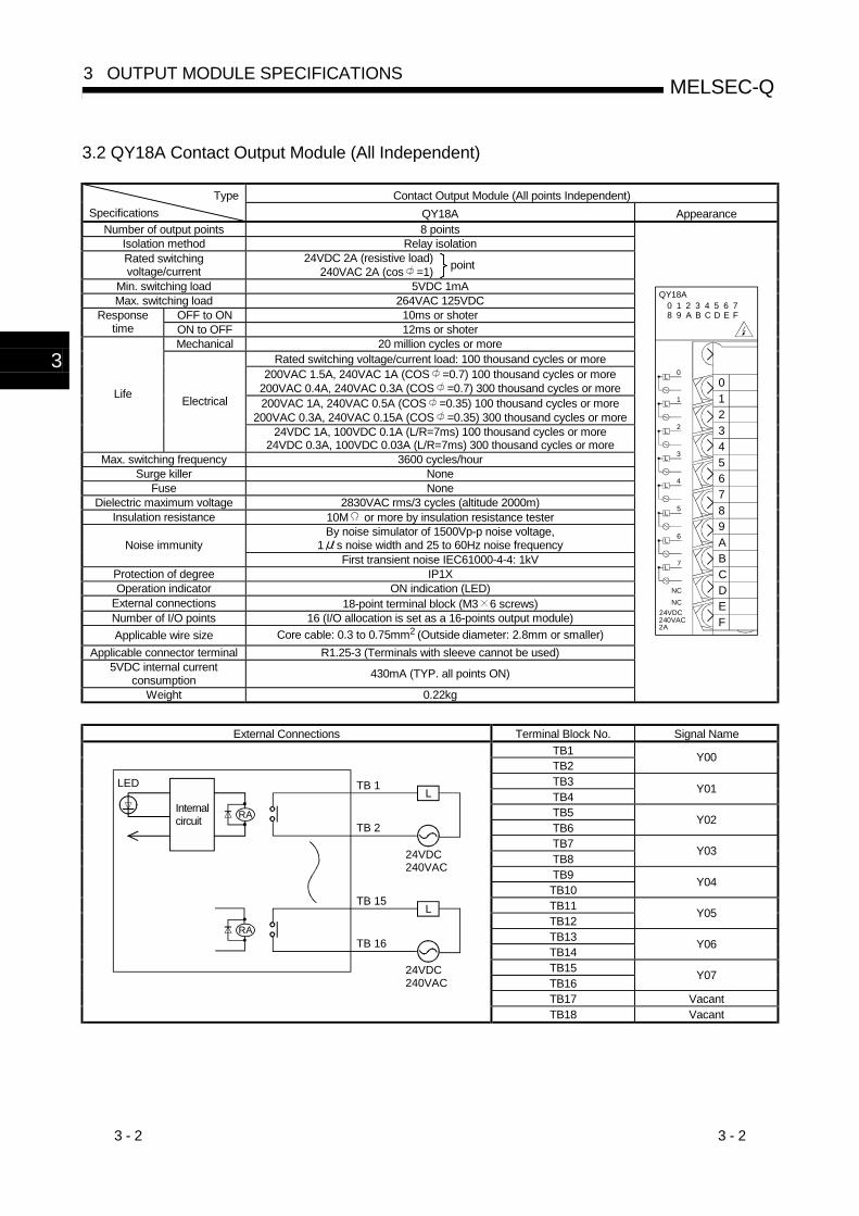
3 - 2 3 - 2
MELSEC-Q 3 OUTPUT MODULE SPECIFICATIONS
3.2 QY18A Contact Output Module (All Independent)
Contact Output Module (All points Independent) Type Specifications QY18A Appearance
Number of output points 8 points Isolation method Relay isolation Rated switching voltage/current
24VDC 2A (resistive load) 240VAC 2A (cos =1) point
Min. switching load 5VDC 1mA Max. switching load 264VAC 125VDC
OFF to ON 10ms or shoter Response time ON to OFF 12ms or shoter
Mechanical 20 million cycles or more Rated switching voltage/current load: 100 thousand cycles or more
200VAC 1.5A, 240VAC 1A (COS =0.7) 100 thousand cycles or more 200VAC 0.4A, 240VAC 0.3A (COS =0.7) 300 thousand cycles or more 200VAC 1A, 240VAC 0.5A (COS =0.35) 100 thousand cycles or more
200VAC 0.3A, 240VAC 0.15A (COS =0.35) 300 thousand cycles or more
Life Electrical
24VDC 1A, 100VDC 0.1A (L/R=7ms) 100 thousand cycles or more 24VDC 0.3A, 100VDC 0.03A (L/R=7ms) 300 thousand cycles or more
Max. switching frequency 3600 cycles/hour Surge killer None
Fuse None Dielectric maximum voltage 2830VAC rms/3 cycles (altitude 2000m)
Insulation resistance 10M or more by insulation resistance tester By noise simulator of 1500Vp-p noise voltage,
1 s noise width and 25 to 60Hz noise frequency Noise immunity First transient noise IEC61000-4-4: 1kV
Protection of degree IP1X Operation indicator ON indication (LED)
External connections 18-point terminal block (M3 6 screws) Number of I/O points 16 (I/O allocation is set as a 16-points output module) Applicable wire size Core cable: 0.3 to 0.75mm2 (Outside diameter: 2.8mm or smaller)
Applicable connector terminal R1.25-3 (Terminals with sleeve cannot be used) 5VDC internal current
consumption 430mA (TYP. all points ON)
Weight 0.22kg
QY18A
24VDC
0 1 2 3 4 5 6 78 9 A B C D E F
0123456789ABCDEF
L 7
L 6
L 5
L 4
L 3
L 2
L 1
L 0
NCNC
2A240VAC
External Connections Terminal Block No. Signal Name
TB1 TB2
Y00
TB3 TB4
Y01
TB5 TB6
Y02
TB7 TB8
Y03
TB9 TB10
Y04
TB11 TB12
Y05
TB13 TB14
Y06
TB15 TB16
Y07
TB17 Vacant
TB 1LED
Internalcircuit
24VDC240VAC
RA
L
TB 2
TB 15
24VDC240VAC
L
TB 16RA
TB18 Vacant
3

3 - 3 3 - 3
MELSEC-Q 3 OUTPUT MODULE SPECIFICATIONS
3.3 QY22 TRIAC Output Module
TRIAC Output Module Type Specifications QY22 Appearance
Number of output points 16 points Isolation method Photocoupler
Rated load voltage 100-240VDC (+20/-15%) Maximum load current 0.6A/point, 4.8A/common
Minimum load voltage/current 24VAC 100mA, 100VAC 25mA, 240VAC 25mA Maximum rush current 20A/cycle or less
Leakage current at OFF 3mA or lower (for 240V, 60Hz), 1.5mA or lower (for 120V, 60Hz) Maximum voltage drop at ON 1.5V or lower
OFF to ON 1ms + 0.5Hz or less Response time
ON to OFF 1ms + 0.5Hz or less (rated load, resistance load) Surge killer CR absorber
Fuse None (Attaching a fuse to each external wiring is recommended. Refer to
Section 1.2 (14)) Dielectric maximum voltage 2830VAC rms/3 cycles (altitude 2000m)
Insulation resistance 10M or higher by insulation resistance meter By noise simulator of 1.5kVp-p noise voltage,
1 s noise width and 25 to 60Hz noise frequency Noise immunity First transient noise IEC61000-4-4: 1kV
Protection of degree IP1X Common terminal arrangement 16 points/common (common terminal: TB18)
Number of I/O points 16 (I/O allocation is set as a 16-points output module) Operation indicator ON indication (LED)
External connections 18-point terminal block (M3 6 screws) Applicable wire size Core cable: 0.3 to 0.75mm2 (Outside diameter: 2.8mm or smaller)
Applicable connector terminal R1.25-3 (Terminals with sleeve cannot be used) 5VDC internal current
consumption 250mA (Max., all points ON)
Weight 0.40kg
0
1
2
3
4
5
6
7
8
9
A
B
C
D
E
F
COM
QY22
100VAC240VAC0.6A
L
L
L
L
L
L
L
L
L
L
L
L
L
L
L
L
0 1 2 3 4 5 6 78 9 A B C D E F
0123456789ABCDEF
External Connections Terminal Block Number Signal Name
TB1 Y00 TB2 Y01 TB3 Y02 TB4 Y03 TB5 Y04 TB6 Y05 TB7 Y06 TB8 Y07 TB9 Y08 TB10 Y09 TB11 Y0A TB12 Y0B TB13 Y0C TB14 Y0D TB15 Y0E TB16 Y0F TB17 COM
TB 1
TB16
LED
L
L
TB17
100 to 240VAC
internalcircuit
TB18 Vacant 1: Wire the module taking care so that the wiring does not interfere with the left-side module.

3 - 4 3 - 4
MELSEC-Q 3 OUTPUT MODULE SPECIFICATIONS
3.4 QY40P Transistor Output Module (Sink Type)
Transistor Output Module (Sink Type) Type Specifications QY40P Appearance
Number of output points 16 points Isolation method Photocoupler
Rated load voltage 12-24VDC (+20/-15%) Maximum load current 0.1A/point, 1.6A/common
Maximum inrush current 0.7A, 10ms or less Leakage current at OFF 0.1mA or less
Maximum voltage drop at ON 0.1VDC (TYP.) 0.1A, 0.2VDC (MAX.) 0.1A OFF to ON 1ms or less
Response time ON to OFF 1ms or less (rated load, resistive load)
Surge suppressor Zener diode Fuse No
Voltage 12-24VDC (+20/-15%) (ripple ratio within 5%) External supply power Current 10mA (at 24VDC) (Max. all points ON)
Dielectric withstand voltage 560VAC rms/3 cycles (altitude 2000m (6557.38ft.)) Insulation resistance 10M or more by insulation resistance tester
By noise simulator of 500Vp-p noise voltage, 1 s noise width and 25 to 60Hz noise frequency Noise immunity
First transient noise IEC61000-4-4: 1kV Protection of degree IP2X
Common terminal arrangement 16 points/common (common terminal: TB18)
Protection function Yes (thermal protection, short circuit protection) • Thermal protection is activated in increments of 1 point. • Short circuit protection is activated in increments of 1 point.
Operation indicator ON indication (LED) External connections 18-point terminal block (M3 6 screws) Number of I/O points 16 (I/O allocation is set as a 16-points output module) Applicable wire size 0.3 to 0.75mm2 core (2.8mm (0.11in.) OD max.)
Applicable crimping terminal R1.25-3 (sleeved crimping terminals cannot be used.) 5VDC internal current
consumption 65mA (TYP. all points ON)
Weight 0.16kg
0
1
2
3
4
5
6
7
8
9
A
B
C
D
E
F
COM
0123456789ABCDEF
QY40P
12VDC24VDC0.1A
L
L
L
L
L
L
L
L
L
L
L
L
L
L
L
L
0 1 2 3 4 5 6 78 9 A B C D E F
External Connections Terminal Block Number Signal Name
TB1 Y00 TB2 Y01 TB3 Y02 TB4 Y03 TB5 Y04 TB6 Y05 TB7 Y06 TB8 Y07 TB9 Y08 TB10 Y09 TB11 Y0A TB12 Y0B TB13 Y0C TB14 Y0D TB15 Y0E TB16 Y0F TB17 12/24VDC
TB 1LED
TB17 TB16
L
L
R
TB18
12/24VDC
Internalcircuit
TB18 COM

3 - 5 3 - 5
MELSEC-Q 3 OUTPUT MODULE SPECIFICATIONS
3.5 QY41P Transistor Output Module (Sink Type)
Transistor Output Module (Sink Type) Type Specifications QY41P Appearance
Number of output points 32 points Isolation method Photocoupler
Rated load voltage 12-24VDC (+20/-15%) Maximum load current 0.1A/point, 2A/common
Maximum inrush current 0.7A, 10ms or less Leakage current at OFF 0.1mA or less
Maximum voltage drop at ON 0.1VDC (TYP.) 0.1A, 0.2VDC (MAX.) 0.1A OFF to ON 1ms or less Response time ON to OFF 1ms or less (rated load, resistive load)
Surge suppressor Zener diode Fuse No
Voltage 12-24VDC (+20/-15%) (ripple ratio within 5%) External supply power Current 20mA (at 24VDC)
Dielectric withstand voltage 560VAC rms/3 cycles (altitude 2000m (6557.38ft.)) Insulation resistance 10M or more by insulation resistance tester
By noise simulator of 500Vp-p noise voltage, 1 s noise width and 25 to 60Hz noise frequency Noise immunity
First transient noise IEC61000-4-4: 1kV Protection of degree IP2X
Common terminal arrangement 32 points/common (common terminal: A01, A02) Number of I/O points 32 (I/O allocation is set as a 32-points output module)
Protection function Yes (thermal protection, short circuit protection) • Thermal protection is activated in increments of 1 point. • Short circuit protection is activated in increments of 1 point.
Operation indicator ON indication (LED) External connections 40-pin connector Applicable wire size 0.3mm2 (For A6CON1 or A6CON4)
External wiring connector A6CON1, A6CON2, A6CON3, A6CON4 (optional) Applicable connector/terminal
block conversion module A6TBXY36, A6TBXY54
5VDC internal current consumption 105mA (TYP. all points ON)
Weight 0.15kg
QY41P
12/24VDC0.1A
QY41P
0 1 2 3 4 5 6 78 9 A B C D E F0 1 2 3 4 5 6 78 9 A B C D E F
External Connections Pin-Outs Pin No. Signal No. Pin No. Signal No.
B20 Y00 A20 Y10 B19 Y01 A19 Y11 B18 Y02 A18 Y12 B17 Y03 A17 Y13 B16 Y04 A16 Y14 B15 Y05 A15 Y15 B14 Y06 A14 Y16 B13 Y07 A13 Y17 B12 Y08 A12 Y18 B11 Y09 A11 Y19 B10 Y0A A10 Y1A B09 Y0B A09 Y1B B08 Y0C A08 Y1C B07 Y0D A07 Y1D B06 Y0E A06 Y1E B05 Y0F A05 Y1F B04 Vacant A04 Vacant B03 Vacant A03 Vacant B02 12/24VDC A02 COM
B20LED
A05
L
L
R
A01,A02
12/24VDC
B01,B02
Internalcircuit
A20A19A18A17A16A15A14A13A12A11A10A9A8A7A6A5A4A3A2A1
B20B19B18B17B16B15B14B13B12B11B10B9B8B7B6B5B4B3B2B1
Module front view
B01 12/24VDC A01 COM : When using A6CON2 or A6CON3, refer to Chapter 7.

3 - 6 3 - 6
MELSEC-Q 3 OUTPUT MODULE SPECIFICATIONS
3.6 QY42P Transistor Output Module (Sink Type)
Transistor Output Module (Sink Type) Type Specifications QY42P Appearance
Number of output points 64 points Isolation method Photocoupler
Rated load voltage 12-24VDC (+20/-15%) Maximum load current 0.1A/point, 2A/common
Maximum inrush current 0.7A, 10ms or less Leakage current at OFF 0.1mA or less
Maximum voltage drop at ON 0.1VDC (TYP.) 0.1A, 0.2VDC (MAX.) 0.1A OFF to ON 1ms or less Response time ON to OFF 1ms or less (rated load, resistive load)
Surge suppressor Zener diode Fuse No
Voltage 12-24VDC (+20/-15%) (ripple ratio within 5%) External supply power Current 20mA (at 24VDC)/common
Dielectric withstand voltage 560VAC rms/3 cycles (altitude 2000m (6557.38ft.)) Insulation resistance 10M or more by insulation resistance tester
By noise simulator of 500Vp-p noise voltage, 1 s noise width and 25 to 60Hz noise frequency Noise immunity
First transient noise IEC61000-4-4: 1kV Protection of degree IP2X
Common terminal arrangement 32 points/common (common terminal: 1A01, 1A02, 2A01, 2A02) Number of I/O points 64 (I/O allocation is set as a 64-points output module)
Protection function Yes (thermal protection, short circuit protection) • Thermal protection is activated in increments of 1 point. • Short circuit protection is activated in increments of 1 point.
Operation indicator ON indication (LED), 32 point switch-over using switch External connections 40-pin connector Applicable wire size 0.3mm2 (For A6CON1 or A6CON4) 3
External wiring connector A6CON1, A6CON2, A6CON3, A6CON4 (optional) Applicable connector/terminal
block conversion module A6TBXY36, A6TBXY54
5VDC internal current consumption 150mA (TYP. all points ON)
Weight 0.17kg
QY42P
12/24VDC0.1A
QY42PDISPLAY
F L
0 1 2 3 4 5 6 78 9 A B C D E F0 1 2 3 4 5 6 78 9 A B C D E F
External Connections Pin-Outs Pin No.
Sig-nal No.
Pin No.
Sig-nal No.
Pin No.
Sig-nal No.
Pin No.
Sig-nal No.
1B20 Y00 1A20 Y10 2B20 Y20 2A20 Y30 1B19 Y01 1A19 Y11 2B19 Y21 2A19 Y31 1B18 Y02 1A18 Y12 2B18 Y22 2A18 Y32 1B17 Y03 1A17 Y13 2B17 Y23 2A17 Y33 1B16 Y04 1A16 Y14 2B16 Y24 2A16 Y34 1B15 Y05 1A15 Y15 2B15 Y25 2A15 Y35 1B14 Y06 1A14 Y16 2B14 Y26 2A14 Y36 1B13 Y07 1A13 Y17 2B13 Y27 2A13 Y37 1B12 Y08 1A12 Y18 2B12 Y28 2A12 Y38 1B11 Y09 1A11 Y19 2B11 Y29 2A11 Y39 1B10 Y0A 1A10 Y1A 2B10 Y2A 2A10 Y3A 1B09 Y0B 1A09 Y1B 2B09 Y2B 2A09 Y3B 1B08 Y0C 1A08 Y1C 2B08 Y2C 2A08 Y3C 1B07 Y0D 1A07 Y1D 2B07 Y2D 2A07 Y3D 1B06 Y0E 1A06 Y1E 2B06 Y2E 2A06 Y3E 1B05 Y0F 1A05 Y1F 2B05 Y2F 2A05 Y3F 1B04 Vacant 1A04 Vacant 2B04 Vacant 2A04 Vacant 1B03 Vacant 1A03 Vacant 2B03 Vacant 2A03 Vacant
1B02 12/24VDC 1A02 COM1 2B02 12/24
VDC 2A02 COM2
B20
A05
L
L
R
A01,A02B01,B02
LED
SW
Internalcircuit
Left side(first half)
Right side(latter half)
Indicationselectorcircuit
12/24VDC2 The above diagram shows the first half of 32 points (F). The latter half of 32 points (L) are similar.
A20A19A18A17A16A15A14A13A12A11A10A9A8A7A6A5A4A3A2A1
B20B19B18B17B16B15B14B13B12B11B10B9B8B7B6B5B4B3B2B1
Module front view
1B01 12/24VDC 1A01 COM1 2B01 12/24
VDC 2A01 COM2
1: Pin number of 1 indicates that of the left-hand side connector, and pin number of 2 indicates that of the right-hand side connector.
2: Selection of left-hand (F) side provides the first half (Y00 to Y1F) LED indications, and selection of right-hand (L) side provides the latter half (Y20 to Y3F) LED indications.
3: When using A6CON2 or A6CON3, refer to Chapter 7.

3 - 7 3 - 7
MELSEC-Q 3 OUTPUT MODULE SPECIFICATIONS
3.7 QY50 Transistor Output Module (Sink Type)
Transistor Output Module (Sink Type) Type Specifications QY50 Appearance
Number of output points 16 points Isolation method Photocoupler
Rated load voltage 12-24VDC (+20/-15%) Maximum load current 0.5A/point, 4A/common
Maximum inrush current 4A, 10ms or less Leakage current at OFF 0.1mA or less
Maximum voltage drop at ON 0.2VDC (TYP.) 0.5A, 0.3VDC (MAX.) 0.5A OFF to ON 1ms or less
Response time ON to OFF 1ms or less (rated load, resistive load)
Surge suppressor Zener diode Fuse 6.7A (unchangeable) (fuse blow capacity: 50A)
Fuse blow indication Yes (When fuse blows, LED indicates it and signal is output to CPU) Voltage 12-24VDC (+20/-15%) (ripple ratio within 5%) External supply
power Current 20mA (at 24VDC) Dielectric withstand voltage 560VAC rms/3 cycles (altitude 2000m (6557.38ft.))
Insulation resistance 10M or more by insulation resistance tester By noise simulator of 500Vp-p noise voltage, 1 s noise width
and 25 to 60Hz noise frequency Noise immunity First transient noise IEC61000-4-4: 1kV
Protection of degree IP2X Common terminal arrangement 16 points/common (common terminal: TB18)
Number of I/O points 16 (I/O allocation is set as a 16-points output module) Operation indicator ON indication (LED)
External connections 18-point terminal block (M3 6 screws) Applicable wire size 0.3 to 0.75mm2 core (2.8mm (0.11in.) OD max.)
Applicable crimping terminal R1.25-3 (sleeved crimping terminals cannot be used.) 5VDC internal current
consumption 80mA (TYP. all points ON)
Weight 0.17kg
0
1
2
3
4
5
6
7
8
9
A
B
C
D
E
F
COM
QY50
12VDC24VDC0.5A
L
L
L
L
L
L
L
L
L
L
L
L
L
L
L
L
FUSE
0 1 2 3 4 5 6 78 9 A B C D E F
0123456789ABCDEF
External Connections Terminal Block Number Signal Name
TB1 Y00 TB2 Y01 TB3 Y02 TB4 Y03 TB5 Y04 TB6 Y05 TB7 Y06 TB8 Y07 TB9 Y08 TB10 Y09 TB11 Y0A TB12 Y0B TB13 Y0C TB14 Y0D TB15 Y0E TB16 Y0F TB17 12/24VDC
TB 1LED
TB17 TB16
L
L
TB18
12/24VDC
R
R
Internalcircuit
Fuse
TB18 COM

3 - 8 3 - 8
MELSEC-Q 3 OUTPUT MODULE SPECIFICATIONS
3.8 QY68A Transistor Output Module (All Points Independent, Sink/Source Type)
Transistor Output Module (All Points Independent, Sink/Source Type) Type Specifications QY68A Appearance
Number of output points 8 points Isolation method Photocoupler
Rated load voltage 5-24VDC (+20/-10%) Maximum load current 2A/point, 8A/unit
Maximum inrush current 8A, 10ms or less Leakage current at OFF 0.1mA or less
Maximum voltage drop at ON 0.3VDC (MAX.) 2A OFF to ON 3ms or less
Response time ON to OFF 10ms or less (resistive load)
Surge suppressor Zener diode
Fuse None (Attaching a fuse to external wiring is recommended. Refer to
Section 1.2 (15)) External supply power None
Dielectric withstand voltage 560VAC rms/3 cycles (altitude 2000m (6557.38ft.)) Insulation resistance 10M or more by insulation resistance tester
By noise simulator of 500Vp-p noise voltage, 1 s noise width and 25 to 60Hz noise frequency Noise immunity
First transient noise IEC61000-4-4: 1kV Protection of degree IP2X
Common terminal arrangement All points Independent Number of I/O points 16 (I/O allocation is set as a 16-points output module) Operation indicator ON indication (LED)
External connections 18-point terminal block (M3 6 screws) Applicable wire size 0.3 to 0.75mm2 core (2.8mm (0.11in.) OD max.)
Applicable crimping terminal R1.25-3 (sleeved crimping terminals cannot be used.) 5VDC internal current
consumption 110mA (TYP. all points ON)
Weight 0.14kg
QY68A
5/12/24VDC 2A
0 1 2 3 4 5 6 7
0123456789ABCDEF
L 0
NC
NC
L 1
L 2
L 3
L 4
L 5
L 6
L 7
External Connections Terminal Block Number Signal Name
TB1 TB2
Y00
TB3 TB4
Y01
TB5 TB6
Y02
TB7 TB8
Y03
TB9 TB10
Y04
TB11 TB12
Y05
TB13 TB14
Y06
TB15 TB16
Y07
TB17 Vacant
TB 1LED
L
R
R
TB16 L
TB15
TB 2
Internalcircuit
Sink
Source
TB18 Vacant

3 - 9 3 - 9
MELSEC-Q 3 OUTPUT MODULE SPECIFICATIONS
3.9 QY70 Transistor Output Module (Sink Type)
Transistor Output Module (Sink Type) Type Specifications QY70 Appearance
Number of output points 16 points Isolation method Photocoupler
Rated load voltage 5/12VDC (+25/-10%) Maximum load current 16mA/point, 256mA/common
Maximum inrush current 40mA, 10ms or less Output voltage at OFF VOH: 3.5VDC (VCC=5VDC, IOH=0.4mA)
Maximum voltage drop at ON VOL: 0.3VDC OFF to ON 0.5ms or less
Response time ON to OFF 0.5ms or less (resistive load)
Surge suppressor None Fuse 1.6A (unchangeable) (fuse blow capacity: 50A)
Fuse blow indication Yes (When fuse blows, LED indicates it and signal is output to CPU) Voltage 5/12VDC (+25/-10%) (ripple ratio within 5%) External supply
power Current 90mA (at 12VDC) (Max. all points ON) Dielectric withstand voltage 560VAC rms/3 cycles (altitude 2000m (6557.38ft.))
Insulation resistance 10M or more by insulation resistance tester By noise simulator of 500Vp-p noise voltage, 1 s noise width
and 25 to 60Hz noise frequency Noise immunity First transient noise IEC61000-4-4: 1kV
Protection of degree IP2X Common terminal arrangement 16 points/common (common terminal: TB18)
Operation indicator ON indication (LED) External connections 18-point terminal block (M3 6 screws) Number of I/O points 16 (I/O allocation is set as a 16-points output module) Applicable wire size 0.3 to 0.75mm2 core (2.8mm (0.11in.) OD max.)
Applicable crimping terminal R1.25-3 (sleeved crimping terminals cannot be used.) 5VDC internal current
consumption 95mA (TYP. all points ON)
Weight 0.14kg
0
1
2
3
4
5
6
7
8
9
A
B
C
D
E
F
COM
QY70
5VDC12VDC16mA
L
L
L
L
L
L
L
L
L
L
L
L
L
L
L
L
FUSE
0 1 2 3 4 5 6 78 9 A B C D E F
0123456789ABCDEF
External Connections Terminal Block Number Signal Name
TB1 Y00 TB2 Y01 TB3 Y02 TB4 Y03 TB5 Y04 TB6 Y05 TB7 Y06 TB8 Y07 TB9 Y08 TB10 Y09 TB11 Y0A TB12 Y0B TB13 Y0C TB14 Y0D TB15 Y0E TB16 Y0F TB17 5/12VDC
TB 1LED
TB17
TB16L
TB18
5/12VDC
R
R3.3k
R
L
Internalcircuit
FUSE
TB18 COM

3 - 10 3 - 10
MELSEC-Q 3 OUTPUT MODULE SPECIFICATIONS
3.10 QY71 Transistor Output Module (Sink Type)
Transistor Output Module (Sink Type) Type Specifications QY71 Appearance
Number of output points 32 points Isolation method Photocoupler
Rated load voltage 5/12VDC (+25/-10%) Maximum load current 16mA/point, 512mA/common
Maximum inrush current 40mA, 10ms or less Output voltage at OFF VOH: 3.5VDC (VCC=5VDC, IOH=0.4mA)
Maximum voltage drop at ON VOL: 0.3VDC OFF to ON 0.5ms or less Response time ON to OFF 0.5ms or less (resistive load)
Surge suppressor None Fuse 1.6A (unchangeable) (fuse blow capacity: 50A)
Fuse blow indication Yes (When fuse blows, LED indicates it and signal is output to CPU) Voltage 5/12VDC (+25/-10%) (ripple ratio within 5%) External supply
power Current 170mA (at 12VDC) Dielectric withstand voltage 560VAC rms/3 cycles (altitude 2000m (6557.38ft.))
Insulation resistance 10M or more by insulation resistance tester By noise simulator of 500Vp-p noise voltage, 1 s noise width
and 25 to 60Hz noise frequency Noise immunity First transient noise IEC61000-4-4: 0.25kV
Protection of degree IP2X Common terminal arrangement 32 points/common (common terminal: A01, A02)
Number of I/O points 32 (I/O allocation is set as a 32-points output module) Operation indicator ON indication (LED)
External connections 40-pin connector Applicable wire size 0.3mm2 (For A6CON1 or A6CON4)
External wiring connector A6CON1, A6CON2, A6CON3, A6CON4 (optional) 5VDC internal current
consumption 150mA (TYP. all points ON)
Weight 0.14kg
QY71
5/12VDC16mA
QY71
0 1 2 3 4 5 6 78 9 A B C D E F0 1 2 3 4 5 6 78 9 A B C D E F
FUSE
External Connections Pin-Outs Pin No. Signal No. Pin No. Signal No.
B20 Y00 A20 Y10 B19 Y01 A19 Y11 B18 Y02 A18 Y12 B17 Y03 A17 Y13 B16 Y04 A16 Y14 B15 Y05 A15 Y15 B14 Y06 A14 Y16 B13 Y07 A13 Y17 B12 Y08 A12 Y18 B11 Y09 A11 Y19 B10 Y0A A10 Y1A B09 Y0B A09 Y1B B08 Y0C A08 Y1C B07 Y0D A07 Y1D B06 Y0E A06 Y1E B05 Y0F A05 Y1F B04 Vacant A04 Vacant B03 Vacant A03 Vacant B02 5/12VDC A02 COM
B20LED
B01,B02A05 L
A01,A02
5/12VDC
R
R3.3k
R
L
Internalcricuit
FUSE
A20A19A18A17A16A15A14A13A12A11A10A9A8A7A6A5A4A3A2A1
B20B19B18B17B16B15B14B13B12B11B10B9B8B7B6B5B4B3B2B1
Module front view
B01 5/12VDC A01 COM : When using A6CON2 or A6CON3, refer to Chapter 7.

3 - 11 3 - 11
MELSEC-Q 3 OUTPUT MODULE SPECIFICATIONS
3.11 QY80 Transistor Output Module (Source Type)
Transistor Output Module (Source Type) Type Specifications QY80 Appearance
Number of output points 16 points Isolation method Photocoupler
Rated load voltage 12-24VDC (+20/-15%) Maximum load current 0.5A/point, 4A/common
Maximum inrush current 4A, 10ms or less Leakage current at OFF 0.1mA or less
Maximum voltage drop at ON 0.2VDC (TYP.) 0.5A, 0.3VDC (MAX.) 0.5A OFF to ON 1ms or less
Response time ON to OFF 1ms or less (rated load, resistive load)
Surge suppressor Zener diode Fuse 6.7A (unchangeable) (fuse blow capacity: 50A)
Fuse blow indication Yes (When fuse blows, LED indicates it and signal is output to CPU) Voltage 12-24VDC (+20/-15%) (ripple ratio within 5%) External supply
power Current 20mA (at 24VDC) Dielectric withstand voltage 560VAC rms/3 cycles (altitude 2000m (6557.38ft.))
Insulation resistance 10M or more by insulation resistance tester By noise simulator of 500Vp-p noise voltage, 1 s noise width
and 25 to 60Hz noise frequency Noise immunity First transient noise IEC61000-4-4: 1kV
Protection of degree IP2X Common terminal arrangement 16 points/common (common terminal: TB17)
Number of I/O points 16 (I/O allocation is set as a 16-points output module) Operation indicator ON indication (LED)
External connections 18-point terminal block (M3 6 screws) Applicable wire size 0.3 to 0.75mm2 core (2.8mm (0.11in.) OD max.)
Applicable crimping terminal R1.25-3 (sleeved crimping terminals cannot be used.) 5VDC internal current
consumption 80mA (TYP. all points ON)
Weight 0.17kg
0
1
2
3
4
5
6
7
8
9
A
B
C
D
E
F
COM
QY80
12VDC24VDC0.5A
L
L
L
L
L
L
L
L
L
L
L
L
L
L
L
L+-
FUSE
0 1 2 3 4 5 6 78 9 A B C D E F
0123456789ABCDEF
External Connections Terminal Block Number Signal Name
TB1 Y00 TB2 Y01 TB3 Y02 TB4 Y03 TB5 Y04 TB6 Y05 TB7 Y06 TB8 Y07 TB9 Y08 TB10 Y09 TB11 Y0A TB12 Y0B TB13 Y0C TB14 Y0D TB15 Y0E TB16 Y0F TB17 COM
LED
TB17 TB16 L
TB18
TB 1L
12/24VDC
R
RInternalcircuit
Fuse
TB18 0V

3 - 12 3 - 12
MELSEC-Q 3 OUTPUT MODULE SPECIFICATIONS
3.12 QY81P Transistor Output Module (Source Type)
Transistor Output Module (Source Type) Type Specifications QY81P Appearance
Number of output points 32 points Isolation method Photocoupler
Rated load voltage 12-24VDC (+20/-15%) Maximum load current 0.1A/point, 2A/common
Maximum inrush current 0.7A, 10ms or less Leakage current at OFF 0.1mA or less
Maximum voltage drop at ON 0.1VDC (TYP.) 0.1A, 0.2VDC (MAX.) 0.1A OFF to ON 1ms or less Response time ON to OFF 1ms or less (rated load, resistive load)
Surge suppressor Zener diode Fuse No
Voltage 12-24VDC (+20/-15%) (ripple ratio within 5%) External supply power Current 40mA (at 24VDC)
Dielectric withstand voltage 560VAC rms/3 cycles (altitude 2000m (6557.38ft.)) Insulation resistance 10M or more by insulation resistance tester
By noise simulator of 500Vp-p noise voltage, 1 s noise width and 25 to 60Hz noise frequency Noise immunity
First transient noise IEC61000-4-4: 1kV Protection of degree IP2X
Common terminal arrangement 32 points/common (common terminal: 17, 18, 36) Number of I/O points 32 (I/O allocation is set as a 32-points output module)
Protection function Yes (thermal protection, short circuit protection) • Thermal protection is activated in increments of 2 points. • Short circuit protection is activated in increments of 1 point.
Operation indicator ON indication (LED) External connections 37-pin D-sub connector Applicable wire size 0.3mm2 (For A6CON1E)
External wiring connector A6CON1E, A6CON2E, A6CON3E (optional) Applicable connector/terminal
block conversion module A6TBY36-E, A6TBY54-E
5VDC internal current consumption 95mA (TYP. all points ON)
Weight 0.15kg
QY81P
12/24VDC0.1A
QY81P
0 1 2 3 4 5 6 78 9 A B C D E F0 1 2 3 4 5 6 78 9 A B C D E F
Derating Chart Pin-Outs Pin No. Signal No. Pin No. Signal No.
1 Y00 9 Y10 20 Y01 28 Y11 2 Y02 10 Y12 21 Y03 29 Y13 3 Y04 11 Y14 22 Y05 30 Y15 4 Y06 12 Y16 23 Y07 31 Y17 5 Y08 13 Y18 24 Y09 32 Y19 6 Y0A 14 Y1A 25 Y0B 33 Y1B 7 Y0C 15 Y1C 26 Y0D 34 Y1D 8 Y0E 16 Y1E 27 Y0F 35 Y1F 17 COM 37 0V 36 COM 19 0V
LED
L
L
12/24VDC
R
17,18,36
19,37
35
1
Internalcircuit
373635343332313029282726252423222120
19181716151413121110987654321
Module front view
18 COM : When using A6CON2E or A6CON3E, refer to Chapter 7.

3 - 13 3 - 13
MELSEC-Q 3 OUTPUT MODULE SPECIFICATIONS
MEMO

4 - 1 4 - 1
MELSEC-Q 4 INPUT/OUTPUT CONPOSITE MODULE
4. INPUT/OUTPUT CONPOSITE MODULE 4.1 QH42P I/O Module
(1) DC Input Specification (Positive Common Type) Type
Specifications QH42P I/O Module (Input Specification)
Number of input points 32 points Insulation method Photocoupler
Rated input voltage 24VDC (+20/-15%, ripple ratio within 5%) Rated input current Approx. 4mA
Input derating See the derating chart. ON voltage/ON current 19V or higher/3mA or higher
OFF voltage/OFF current 11V or lower/1.7mA or lower Input resistance Approx. 5.6k
OFF ON 1ms/5ms/10ms/20ms/70ms or less (CPU parameter setting) 1 Initial setting is 10ms Response time
ON OFF 1ms/5ms/10ms/20ms/70ms or less (CPU parameter setting) 1 Initial setting is 10ms
Dielectric maximum voltage 560VAC rms/3 cycles (altitude 2000m) Insulation resistance 10M or more by insulation resistance tester
By noise simulator of 500Vp-p noise voltage, 1 s noise width and 25 to 60Hz noise frequency Noise immunity First transient noise IEC61000-4-4: 1kV
Protection of degree IP2X Common terminal arrangement 32 points/common (common terminal: 1B01, 1B02) Number of I/O occupied points 32 points (For I/O allocation on I/O mixed module, set 32 points.)
Operation indicator ON indication (LED), 32-point switchover using switch External connections 40-pin connector Applicable wire size 0.3mm2 (For A6CON1 or A6CON4) 4
External wiring connector A6CON1, A6CON2, A6CON3, A6CON4 (optional) Mixed connector/terminal block
conversion module A6TBXY36, A6TBXY54, A6TBX70
5VDC internal current consumption 130mA (TYP, all points ON)
Weight 0.20kg
External Connections Derating Chart
R
R1B20
1B02
1B01
LED
SW+-
Internalcircuit
1A05 Indicationselectorcircuit
Left side (first half)Right side (latter half)12/24VDC
2B20
2A05
L
L
R
12/24VDC
2B022B012A022A01 +-
Internalcircuit
9080706050
100
4010 20 30 40 500 55
Ambient temperature
28.8VDC
(°C)
(%)
ON
Rat
io
1: For the setting method, refer to the Section 1.3.1. 2: Selection of left-hand (F) side provides the first half (X00 to X1F) LED indications, and selection of right-hand (L) side provides the
latter half (Y00 to Y1F) LED indications. 3: When using the main module, use the constructions listed in Section 1.2 (13). 4: When using A6CON2 or A6CON3, refer to Chapter 7.
4

4 - 2 4 - 2
MELSEC-Q 4 INPUT/OUTPUT CONPOSITE MODULE
(2) Transistor Output Specification (Sink Type)
Type Specifications QH42P I/O Module (Output Specification) Appearance
Number of output points 32 points Insulation method Photocoupler Rated load voltage 12-24VDC (+20/-15%) Max. load current 0.1A/point, 2A/common Max. rush current 0.7A/10ms or less
Leakage current at OFF 0.1mA or lower Max. voltage drop at ON 0.1VDC (TYP.) 0.1A, 0.2VDC (MAX.) 0.1A
OFF ON 1ms or shorter Response time ON OFF 1ms or shorter (rated load, resistance load)
Surge killer Zener diode Fuse None
Voltage 12-24VDC (+20/-15%) (ripple ratio within 5%) External power supply Current 15mA (at 24VDC)/common (Max., all points ON)
Common terminal arrangement 32 points/common (common terminal: 2A01, 2A02)
Protection function Provided (thermal protector, protector against shortcircuit) • Thermal protectors operate independently of each other. • Protectors against shortcircuit operate independently of each other.
QH42P
24VDC4mA12/24VDC0.1A
QY42PDISPLAY
F L
0 1 2 3 4 5 6 78 9 A B C D E F0 1 2 3 4 5 6 78 9 A B C D E F
Pin-Outs Pin No. Signal No. Pin No. Signal No. Pin No. Signal No. Pin No. Signal No.
1B20 X00 1A20 X10 2B20 Y00 2A20 Y10 1B19 X01 1A19 X11 2B19 Y01 2A19 Y11 1B18 X02 1A18 X12 2B18 Y02 2A18 Y12 1B17 X03 1A17 X13 2B17 Y03 2A17 Y13 1B16 X04 1A16 X14 2B16 Y04 2A16 Y14 1B15 X05 1A15 X15 2B15 Y05 2A15 Y15 1B14 X06 1A14 X16 2B14 Y06 2A14 Y16 1B13 X07 1A13 X17 2B13 Y07 2A13 Y17 1B12 X08 1A12 X18 2B12 Y08 2A12 Y18 1B11 X09 1A11 X19 2B11 Y09 2A11 Y19 1B10 X0A 1A10 X1A 2B10 Y0A 2A10 Y1A 1B09 X0B 1A09 X1B 2B09 Y0B 2A09 Y1B 1B08 X0C 1A08 X1C 2B08 Y0C 2A08 Y1C 1B07 X0D 1A07 X1D 2B07 Y0D 2A07 Y1D 1B06 X0E 1A06 X1E 2B06 Y0E 2A06 Y1E 1B05 X0F 1A05 X1F 2B05 Y0F 2A05 Y1F 1B04 Vacant 1A04 Vacant 2B04 Vacant 2A04 Vacant 1B03 Vacant 1A03 Vacant 2B03 Vacant 2A03 Vacant 1B02 COM1 1A02 Vacant 2B02 12/24VDC 2A02 COM2
A20A19A18A17A16A15A14A13A12A11A10A9A8A7A6A5A4A3A2A1
B20B19B18B17B16B15B14B13B12B11B10B9B8B7B6B5B4B3B2B1
Module front view
1B01 COM1 1A01 Vacant 2B01 12/24VDC 2A01 COM2 1: Pin number of 1 indicates that of the left-hand side connector, and pin number of 2 indicates that of the right-hand
side connector.
4

4 - 3 4 - 3
MELSEC-Q 4 INPUT/OUTPUT CONPOSITE MODULE
4.2 QX48Y57 I/O Module
(1) DC Input Specification (Positive Common Type) Type
Specifications QX48Y57 I/O Module (Input Specification) Appearance
Number of input points 8 points Insulation method Photocoupler
Rated input voltage 24VDC (+20/-15%, ripple ratio within 5%) Rated input current Approx. 4mA
Input derating None ON voltage/ON current 19V or higher/3mA or higher
OFF voltage/OFF current 11V or lower/1.7mA or lower Input resistance Approx. 5.6k
OFF ON 1ms/5ms/10ms/20ms/70ms or less (CPU parameter setting) 1 Initial setting is 10ms Response
time ON OFF 1ms/5ms/10ms/20ms/70ms or less (CPU parameter setting) 1
Initial setting is 10ms Dielectric maximum voltage 560VAC rms/3 cycles (altitude 2000m)
Insulation resistance 10M or more by insulation resistance tester By noise simulator of 500Vp-p noise voltage,
1 s noise width and 25 to 60Hz noise frequency Noise immunity First transient noise IEC61000-4-4: 1kV
Protection of degree IP2X Common terminal
arrangement 8 points/common (common terminal: TB9)
Number of I/O occupied points 16 points (For I/O allocation on I/O mixed module, set 16 points.)
Operation indicator ON indication (LED) External connections 18-point terminal block (M3 6 screw) Applicable wire size Core cable: 0.3 to 0.75mm2 (Outside diameter: 2.8mm or smaller)
Applicable connector terminal R1.25-3 (Terminals with sleeve cannot be used) 5VDC internal current
consumption 80mA (TYP, all points ON)
Weight 0.20kg
0
1
2
3
4
5
6
7
8
9
A
B
C
D
E
QX48Y57
24VDC4mA12/24VDC0.5A
L
L
L
L
L
L
L
FUSE
0 1 2 3 4 5 6 78 9 A B C D E F
0123456789ABCDEF
COM+-
COM
External Connections Terminal Block No. Signal Name
TB1 X00 TB2 X01 TB3 X02 TB4 X03 TB5 X04 TB6 X05 TB7 X06 TB8 X07 TB9 COM1 TB10 Y08 TB11 Y09 TB12 Y0A TB13 Y0B TB14 Y0C TB15 Y0D TB16 Y0E TB17 12/24VDC
LEDR
TB 1
TB 9
24VDC
R
TB 8
Internalcircuit
TB17TB16 L
TB18
TB10L
12/24VDCR
Fuse
R
TB18 COM2 1: For the setting method, refer to the Section 1.3.1. 2: When using the main module, use the constructions listed in Section 1.2 (13).

4 - 4 4 - 4
MELSEC-Q 4 INPUT/OUTPUT CONPOSITE MODULE
(2) Transistor Output Specifications (Sink Type)
Type Specifications QX48Y57 I/O Module (Output Specification)
Number of output points 7 points Insulation method Photocoupler Rated load voltage 12-24VDC (+20/-15%) Max. load current 0.5A/point, 2A/common Max. rush current 4A/10ms or less
Leakage current at OFF 0.1mA or lower Max. voltage drop at ON 0.2VDC (TYP.) 0.5A, 0.3VDC (MAX.) 0.5A
OFF ON 1ms or shorter Response time ON OFF 1ms or shorter (rated load, resistance load)
Surge killer Zener diode Fuse 4A (Not replaceable) (Fuse breakage capacity: 50A)
Fuse breakage indication Provided (When fuse is broken, LED lights and a signal is output to CPU) 3 Voltage 12-24VDC (+20/-15%) (ripple ratio within 5%) External
power supply Current 10mA (at 24VDC) Common terminal
arrangement 7 points/common (common terminal: TB18)
3: When the external power supply is turned off, fuse breakage is not detected.

5 - 1 5 - 1
MELSEC-Q 5 INTERRUPT MODULE
5. INTERRUPT MODULE
5.1 QI60 Interrupt Module
Interrupt Module Type Specifications QI60 Appearance
Number of input points 16 points Isolation method Photocoupler
Rated input voltage 24VDC (+20/-15%, ripple ratio within 5%) Rated input current Approx. 6mA
Input derating No ON voltage/ON current 19V or higher/4.0mA or higher
OFF voltage/OFF current 11V or lower/1.7mA or lower Input impedance Approx. 3.9k
Set value 1 0.1 0.2 0.4 0.6 1 Typ 0.05ms 0.15ms 0.30ms 0.55ms 1.05ms OFF to ON max 0.10ms 0.20ms 0.40ms 0.60ms 1.20ms Typ 0.15ms 0.20ms 0.35ms 0.60ms 1.10ms
Response time
ON to OFF max 0.20ms 0.30ms 0.50ms 0.70ms 1.30ms
Dielectric withstand voltage 560VAC rms/3 cycles (altitude 2000m (6557.38ft.)) Insulation resistance 10M or more by insulation resistance tester
By noise simulator of 500Vp-p noise voltage, 1 s noise width and 25 to 60Hz noise frequency Noise immunity
First transient noise IEC61000-4-4: 1kV Protection of degree IP2X Common terminal
arrangement 16 points/common (common terminal: TB17)
Number of I/O points 16 (I/O allocation is set as a 16-points interrupt module) 4 Interrupt processing condition Set by setting the CPU parameter switch. 3
Operation indicator ON indication (LED) External connections 18-point terminal block (M3 6 screws) Applicable wire size 0.3 to 0.75mm2 core (2.8mm (0.11in.) OD max.)
Applicable crimping terminal R1.25-3 (sleeved crimping terminals cannot be used.) 5VDC internal current
consumption 60mA (TYP. all points ON)
Weight 0.20kg
0
1
2
3
4
5
6
7
8
9
A
B
C
D
E
F
COM
QI60
NC
24VDC6mA
+-
0 1 2 3 4 5 6 78 9 A B C D E F
0123456789ABCDEF
External Connections Terminal Block Number Signal Name
TB1 X00 TB2 X01 TB3 X02 TB4 X03 TB5 X04 TB6 X05 TB7 X06 TB8 X07 TB9 X08 TB10 X09 TB11 X0A TB12 X0B TB13 X0C TB14 X0D TB15 X0E TB16 X0F TB17 COM
RTB 1 LED
TB17
24VDC
R
TB16
Internalcircuit
TB18 Vacant 1: For usage of the main module, refer to the QCPU (Q-mode) User's Manual (Function Explanation/Program Basics Version). 2: Use the CPU parameter settings to select. (Default: 0.2ms). Refer to Section 1.3.1 for the setting method. 3: For the setting method, refer to the section 1.3.3. 4: When making settings with an SW5D5C-GPPW or earlier GX Developer, select "16 point intelligent module."
5

5 - 2 5 - 2
MELSEC-Q 5 INTERRUPT MODULE
MEMO
5

6 - 1 6 - 1
MELSEC-Q 6 BLANK COVER MODULE
6. BLANK COVER MODULE
This chapter provides the specifications of the blank cover module used to protect the vacant slot (between I/O modules) of the base module from dust.
Table 6.1 Blank Cover Module Specifications
Type Item
QG60
Number of I/O points occupied
16 points
I/O allocation 16 vacant points
Application Used as a dustproof cover for a slot not loaded with an I/O module (especially a vacant slot between modules).
External dimensions (mm (inch))
98 (3.86) (H) 27.4 (1.08) (W) 90 (3.55) (D)
Weight (kg ) 0.07 Load the blank cover module with the connector cover of the base module fitted.
6

6 - 2 6 - 2
MELSEC-Q 6 BLANK COVER MODULE
MEMO
6

7 - 1 7 - 1
MELSEC-Q 7 CONNECTORS
7. CONNECTORS
The 40-pin connectors and 37-pin D-sub connectors used with the input and output modules are to be user-prepared. The following tables list the connector types and applicable models, and introduce crimp-contact and pressure-displacement tools.
(1) 40-pin connectors
(a) 40-pin connectors Type Model Name Applicable Wire Size Applicable Model
Soldering type connector A6CON1 0.3mm2 (AWG#22)
Crimp-contact type connector A6CON2 AWG#24 to 28
Pressure-displacement type connector A6CON3 AWG#28 (twisted) AWG#30 (single wire)
Soldering type connector A6CON4 0.3mm2 (AWG#22)
QX41, QX41-S1, QX42, QX42-S1, QX71, QX72, QX82, QY41P, QY42P,
QY71, QH42P
(b) 40-pin connector crimp-contact and pressure-displacement
tools Type Model Name Contact
Crimp-contact tool FCN-363T-T005/H FCN-367T-T012/H (locator plate) FCN-707T-T001/H (cable cutter)
Pressure-displacement tool
FCN-707T-T101/H (hand press)
FUJITSU COMPONENT LIMITED
(2) 37-pin D-sub connectors
(a) 37-pin D-sub connectors Type Model Name Applicable Wire Size Applicable Model
Soldering type connector A6CON1E 0.3mm2 (AWG#22)
Crimp-contact type connector A6CON2E AWG#24 to 24
Pressure-displacement type connector A6CON3E AWG#28 (twisted) AWG#30 (single wire)
QX81, QY81P
7

7 - 2 7 - 2
MELSEC-Q 7 CONNECTORS
(b) 37-pin D-sub connector crimp-contact and pressure-
displacement tools Type Model Name Contact
Crimp-contact tool 90312-1
91257-1 (die set)
91220-1 (cable cutter) Pressure-displacement tool
91085-2 (hand mini-press)
AMP Incorporated Americas: Worldwide Headquarters of AMP Incorporated Harrisburg, PA, U.S.A. Phone: (717) 564-0100 Fax: (717) 986-7813 Far East: AMP Singapore Pte. Ltd. Singapore Phone: (65) 482-0311 Fax: (65) 482-1012 Europe: AMP Deutschland G.m.b.H. Langen, Germany Phone: (49) 6103-7090 Fax: (49) 6103-709223
7

8 - 1 8 - 1
MELSEC-Q
8 SPECIFICATIONS OF CONNECTOR/TERMINAL BLOCK CONVERTOR MODULES
8. SPECIFICATIONS OF CONNECTOR/TERMINAL BLOCK CONVERTOR
MODULES
8.1 Specifications of Connector/Terminal Block Convertor Modules
This chapter explains the specifications of connector/terminal block convertor modules.
(1) Connector/Terminal Block Convertor Module Specifications Type Details Weight Applicable Models
A6TBXY36 For positive common type input modules and sink type output modules (standard type)
0.4kg
A6TBXY54 For positive common type input modules and sink type output modules (2-wire type)
0.5kg
Q series: QX41, QX41-S1, QX42, QX42-S1, QY41P, QY42P, QH42P
AnS series: A1SX41, A1SX41-S1, A1SX41-S2, A1SX42, A1SX42-S1, A1SX42-S2, A1SX42, A1SX82-S1 A1SY41, A1SY42, A1SY82, A1SH42, A1SH42-S1
A series: AX42, AX42-S1, AY42, AY42-S1, AY42-S2, AY42-S3, AY42-S4, AH42
CC-Link: AJ65SBTCF1-32D, AJ65SBTCF1-32T, AJ65SBC1-32D AJ65SBC1-32T
MELSECNET-MINI: AJ35TC1-32D, AJ35TC1-32T
A6TBX70 For positive common type input modules (3-wire type)
0.6kg
Q series: QX41, QX41-S1, QX42, QX42-S1, QH42P
AnS series: A1SX41, A1SX41-S1, A1SX41-S2, A1SX42, A1SX42-S1, A1SX42-S2, A1SX42, A1SX82-S1, A1SH42, A1SH42-S1
A series: AX42, AX42-S1, AH42 CC-Link: AJ65SBTCF1-32D, AJ65SBC1-32D MELSECNET-MINI: AJ35TC1-32D
A6TBX36-E For negative common type input modules (standard type) 0.4kg
A6TBX54-E For negative common type input modules (2-wire type) 0.5kg
A6TBX70-E For negative common type input modules (3-wire type) 0.6kg
Q series: QX81 AnS series: A1SX81, A1SX81-S1, A1SX81-S2 A series: AX82
A6TBY36-E For source type output modules (standard type) 0.4kg
A6TBY54-E For source type output modules (2-wire type) 0.5kg
Q series: QY81P AnS series: A1SY81 A series: AY82EP
(2) Cable
Type Details Weight Applicable Models AC05TB 0.5 m (19.69 in.), for sink modules 0.17kg AC10TB 1 m (39.37 in.), for sink modules 0.23kg AC20TB 2 m (78.74 in.), for sink modules 0.37kg AC30TB 3 m (118.11 in.), for sink modules 0.51kg AC50TB 5 m (196.85 in.), for sink modules 0.76kg
AC80TB 8 m (314.96 in.), for sink modules (common current not exceeding 0.5 A) 1.2kg
AC100TB 10 m (393.7 in.), for sink modules (common current not exceeding 0.5 A) 1.5kg
A6TBXY36 A6TBXY54 A6TBX70
AC05TB-E 0.5 m (19.69 in.), for source modules 0.17kg AC10TB-E 1 m (39.37 in.), for source modules 0.23kg AC20TB-E 2 m (78.74 in.), for source modules 0.37kg AC30TB-E 3 m (118.11 in.), for source modules 0.51kg AC50TB-E 5 m (196.85 in.), for source modules 0.76kg
A6TBX36-E A6TBY36-E A6TBX54-E A6TBY54-E A6TBX70-E
8

8 - 2 8 - 2
MELSEC-Q
8 SPECIFICATIONS OF CONNECTOR/TERMINAL BLOCK CONVERTOR MODULES
IMPORTANT (1) The number of connectable I/O points is 32 for all connector/terminal block
convertor modules. Two connector/terminal block convertor modules and two cables for connector/terminal block convertor modules are required for 64-point I/O modules.
(2) Though the A1SX81(S1/S2) is used either as a sink or source type, use the A6TBX36-E, A6TBX54-E or A6TBX70-E. The A6TBXY36, A6TBXY54 or A6TBX70 cannot be used.
(3) Though the A1SX82-S1 is used either as a sink or source type, the A6TBXY36/XY54/X70 may be used only when the A1SX82-S1 is used as a sink type. When it is used as a source type, the A6TBXY36/XY54/X70 cannot be used.
(4) Though the A1SY82 is a source type output module, use theA6TBXY36 or A6TBXY54. The A6TBXY36-E or A6TBXY54-E cannot be used.
(5) In the A series, the plus common input module is separately labeled as a sink type input module, and the minus common input module is separately labeled as a source type input module.
(6) When using the A6TBXY70 as a mixed input/output module, use at the input side.
(7) Tighten the module terminal screws to the following torque. Supply line connecting terminal screw (M3.5 screw): Tightening torque 78.4N•cm
8

8 - 3 8 - 3
MELSEC-Q
8 SPECIFICATIONS OF CONNECTOR/TERMINAL BLOCK CONVERTOR MODULES
8.2 Connector/Terminal Block Convertor Module Connection Diagrams
8.2.1 A6TBXY36 (1) When connecting an input
module (2) When connecting an
output module (a) Sink Type
(b) Source Type
Load
OutputModule
InputModule
Load
OutputModule

8 - 4 8 - 4
MELSEC-Q
8 SPECIFICATIONS OF CONNECTOR/TERMINAL BLOCK CONVERTOR MODULES
8.2.2 A6TBXY54 (1) When connecting an input
module
(2) When connecting an
output module (a) Sink Type
(b) Source Type
6
6
OutputModule
InputModule
Load
2-wire type sensor
6OutputModule
Load
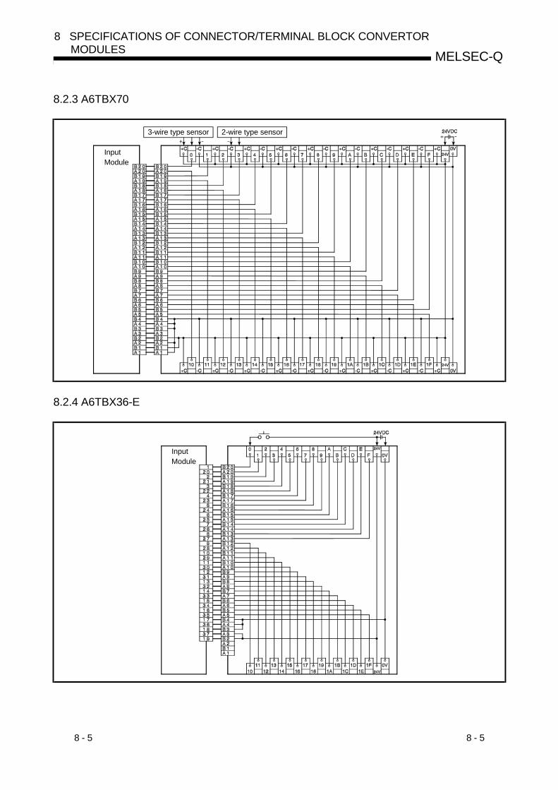
8 - 5 8 - 5
MELSEC-Q
8 SPECIFICATIONS OF CONNECTOR/TERMINAL BLOCK CONVERTOR MODULES
8.2.3 A6TBX70
InputModule
3-wire type sensor 2-wire type sensor
8.2.4 A6TBX36-E
InputModule

8 - 6 8 - 6
MELSEC-Q
8 SPECIFICATIONS OF CONNECTOR/TERMINAL BLOCK CONVERTOR MODULES
8.2.5 A6TBY36-E
OutputModule
Load
8.2.6 A6TBX54-E
6InputModule
2-wire type sensor
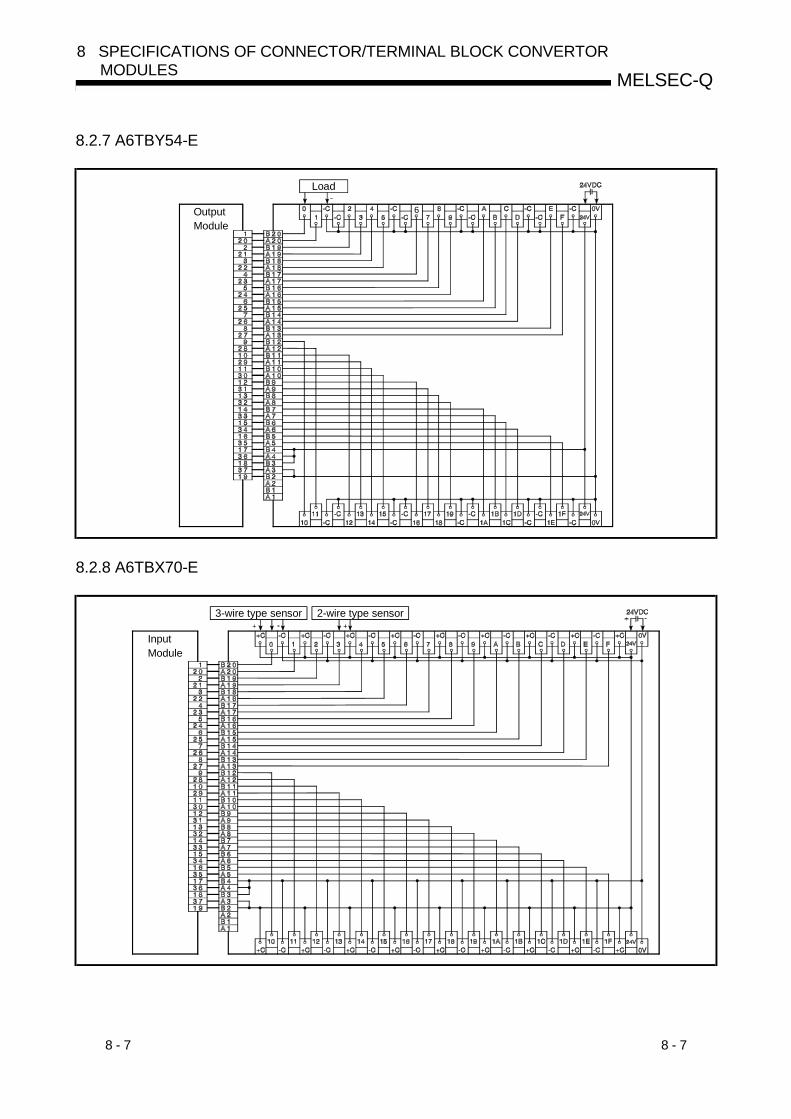
8 - 7 8 - 7
MELSEC-Q
8 SPECIFICATIONS OF CONNECTOR/TERMINAL BLOCK CONVERTOR MODULES
8.2.7 A6TBY54-E
6OutputModule
Load
8.2.8 A6TBX70-E
InputModule
3-wire type sensor 2-wire type sensor

9 - 1 9 - 1
MELSEC-Q
9 SPRING CLAMP TERMINAL BLOCK
9. SPRING CLAMP TERMINAL BLOCK
9.1 Q6TE-18S
The Q6TE-18S shall be used attached to a Q Series terminal block type I/O module or an intelligent function module. Since the Q6TE-18S uses a spring clamp it does not require screw tightening, which greatly reduces the number of wiring procedures.
(1) Compatible Models
The QT6E-18S can be used with the following models: Model type Model name
QX10 QX28 QX40 QX40-S1 QX70 QX80 QY10 QY18A QY22 QY40P QY50 QY68A I/O module QY70 QY80 QX48Y57 QI60 Q62DA Q64DA Q68DAV Q68DAI Q64AD Q68ADV Q68ADI Intelligent function
module Q64TCRT Q64TCRTBW Q64RD
POINT The terminal numbers of the Q6TE-18S correspond to the terminal numbers on the compatible module. For the signal names corresponding to the terminal numbers when connected to an external device, please refer to the User's Manual of the module to use.
(2) Specifications
Item Specifications
Applicable wire size 0.3 to 1.5 mm2 (AWG22 to 16) Wire strip length 8 to 11 mm Mounting screw tightening torque range 66 to 89 N!cm Weight 0.07kg
(3) Removal of Terminal Block and Installation of Q6TE-18S
(a) Removal of terminal block
! Unscrew the two terminal block mounting screws situated at the top and bottom of the terminal block.
! Gently remove the terminal block.
Terminal block
Terminal block mounting screw
Module
9

9 - 2 9 - 2
MELSEC-Q
9 SPRING CLAMP TERMINAL BLOCK
(b) Installation of Q6TE-18S
! Attach the Q6TE-18S to the module. ! Tighten the terminal block mounting screws within the specified torque
range.
Q6TE-18S
Terminal blockmounting screw
Module
(c) Cable Installation Insert the tool into the square shaped hole, which corresponds to the terminal you wish to use. While the tool is inside the hole, insert the wire into the circular shaped hole (as shown below). Remove the tool from the square shaped hole, taking care not to remove the wire. After the wire has been clamped, gently pull the wire to confirm that it is secure.
Square shaped hole
Circular shaped hole
Wire strip length:8mm to 11mm *
Wire
Tool
[Cautions] * Take care that the wire strip length is between 8mm to 11mm.
If the wire strip length is too long, this will expose the bare wire, which increases the risk of electric shock or short circuit. If the wire strip length is too short, this will result in the wire not being securely attached.
(d) Cable removal
Insert the tool into the corresponding square shaped hall until it stops. Pull the wire out of the hall completely.
9

10 - 1 10 - 1
MELSEC-Q 10 NAMES OF MODULE PARTS
10. NAMES OF MODULE PARTS
This chapter explains the names of the I/O module parts.
Terminal block connector 40-pin connector
0
1
2
3
4
5
6
7
8
9
A
B
C
D
E
F
COM
QX10
NC100VAC8mA60Hz7mA50Hz
QX41
24VDC4mA
QX41
QX42
24VDC4mA
QX42DISPLAY
F L123456789
101112131415161718
4)
1) 1)
2)2)2)
3)
7) 7)
5) 5)
6)
1)
0 1 2 3 4 5 6 78 9 A B C D E F
0 1 2 3 4 5 6 78 9 A B C D E F0 1 2 3 4 5 6 78 9 A B C D E F
0 1 2 3 4 5 6 78 9 A B C D E F0 1 2 3 4 5 6 78 9 A B C D E F
7) No. Name Description
1) Module fixing hook Hook used to fix the module to the base unit. (Single-motion installation)
2) I/O indicator LED Indicates the ON/OFF status of I/O and lit when I/O is ON.
3) Terminal block Used to connect power and I/O signal wires.
4) Terminal cover Terminal cover with recording paper
5) 40-pin connector Designed for 32- or 64-point module and used to connect power and I/O signal wires.
6) Indication selector switch Used to switch the LED indications between the first-half 32 points and latter-half 32 points of a 64-point module.
7) Module loading lever Used to load the module into the base unit.
10

10 - 2 10 - 2
MELSEC-Q 10 NAMES OF MODULE PARTS
37-pin D-sub connector
QX81
24VDC4mA
QX81
1)
2)
8)
9)0 1 2 3 4 5 6 78 9 A B C D E F0 1 2 3 4 5 6 78 9 A B C D E F
10)
7) No. Name Description
8) 37-pin D-sub connector Designed for 32 points and used to connect power and I/O signal wires.
9) Module fixing screw hole Used to fix the module to the base unit.
10) Metal fitting Do not touch as this may be deformed.
10

10 - 3 10 - 3
MELSEC-Q 10 NAMES OF MODULE PARTS
A6TB 36
1) 2)
3)
1)2)
4)
0 2 4 6 8 A C E
1 3 5 7 9 B D F
10 12 14 16 18 1A 1C 1E
11 13 15 17 19 1B 1D 1F
0V
24V
24V
0V
A6TB 54
2)1)
1)2)
3)
4)
0 COM 2 4 6 8 A C E 0V
24V1 COM 3 5 7 9 B D FCOM COM COM
11 COM 13 15 17 19 1B 1D 1FCOM COM COM
10 COM 12 14 16 18 1A 1C 1ECOM COM COM COM
24V
0V
COM COM COM COM
No. Name Description
1) Panel mounting hole Used for mounting to panel (for M4 screw). 2) Terminal block Used to connect power and signal wires.
3) 40-pin connector Designed for 32-point module and used to connect power and I/O signal wires.
4) Module fixing hook Used for mounting onto DIN rail.

10 - 4 10 - 4
MELSEC-Q 10 NAMES OF MODULE PARTS
A6TBX70
1)
1)2)
2)
3)
4)
0V
24V
24V
0V
0 1 2 3 4 5 6 7 8 9 A B C D E F
+C +C +C +C +C +C +C +C -C +C-C-C-C-C-C-C-C
10 11 12 13 14 15 16 17 18 19 1A 1B 1C 1D 1E 1F
+C +C +C +C +C +C +C +C -C +C-C-C-C-C-C-C-C
No. Name Description
1) Panel mounting hole Used for mounting to panel (for M4 screw). 2) Terminal block Used to connect power and signal wires.
3) 40-pin connector Designed for 32-point module and used to connect power and I/O signal wires.
4) Module fixing hook Used for mounting onto DIN rail.
Q6TE-18S
17
15
13
11
9
7
5
3
1
18
16
14
12
10
8
6
4
2
Q6TE -18S
1)
2)
3)
No. Name Description
1) Terminal block mounting screw This is for securing Q6TE-18S terminal block to a module
2) Circular shaped hole A hole for inserting wire when wiring
3) Square shaped hole A hole for inserting a tool when wiring

11 - 1 11 - 1
MELSEC-Q 11 I/O MODULE TROUBLESHOOTING
11. I/O MODULE TROUBLESHOOTING
This chapter explains possible problems with I/O circuits and their corrective actions. 11.1 Input Circuit Troubleshooting
This section describes possible problems with input circuits and their corrective actions.
Table 11.1 Input Circuit Problems and Corrective Actions
Condition Cause Corrective Action
Exam
ple
1
Input signal does not turn OFF.
• Leakage current of input switch (e.g. drive by non-contact switch).
Leakagecurrent Input module
AC input
Power supply
• Connect an appropriate resistor which will make the voltage across the terminals of the input module lower than the OFF voltage value.
AC input
Input module
It is recommended to use 0.1 to 47 F + 47 to 120 (1/2W) for the CR constant.
Exam
ple
2
Input signal does not turn OFF.
• Drive by a limit switch with neon lamp.
Leakagecurrent
AC input
Input module
Power suppiy
• Same as Example 1. • Or make up another independent display
circuit.
Exam
ple
3
Input signal does not turn OFF.
• Leakage current due to line capacity of wiring cable. (Line capacity C of twisted pair wire is approx. 100 PF/m).
Leakagecurrent
AC input
Input module
Power supply
• Same as Example 1. • However, leakage current is not generated
when the power supply is located in the input equipment side as shown below.
AC input
Input module
Power supply
11

11 - 2 11 - 2
MELSEC-Q 11 I/O MODULE TROUBLESHOOTING
Table 11.1 Input Circuit Problems and Corrective Actions (Continued)
Condition Cause Corrective Action
Exam
ple
4
Input signal does not turn OFF.
• Drive by switch with LED indicator.
Leakagecurrent
DC input (Positive common)
Input module
• Connect a register which will make the voltage between the input module terminal and common lower than the OFF voltage, as shown below.
Input moduleResistor
DC input (Positive common)
A calculation example of a value for a connected resistor is given on the following page.
Exam
ple
5
Input signal does not turn OFF.
• Sneak path due to the use of two power supplies.
Input moduleE1 E2
E1 E2>
• Use only one power supply. • Connect a sneak path prevention diode.
(Figure below)
Input moduleE1 E2
Exam
ple
6
False input due to noise
Depending on response time setting, noise is imported as input.
Change response time setting. Example 1ms 5ms
(Setting of a shorter response time may produce a higher effect on periodic excessive noise.) If no effects are produced by the above, take basic actions to prevent excessive noise from entering, e.g. avoid bundling the power and I/O cables, and suppress noise by adding surge absorbers to such noise sources as relays and contactors used with the same power supply.)
<Calculation example of Example 4> Consider a switch with LED indicator connected to the QX40, giving a leakage current of 4mA when a 24VDC power is turned on.
QX40
Input moduleLeakagecurrent 4mA
24VDC3.6K
11
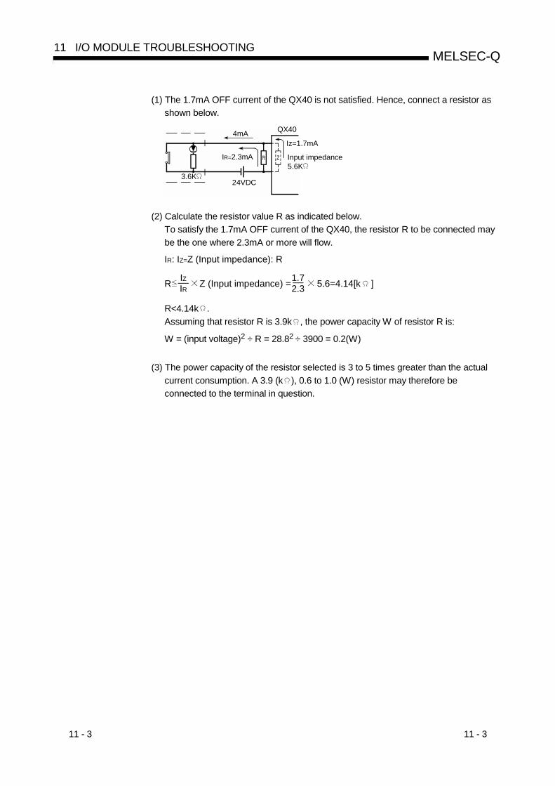
11 - 3 11 - 3
MELSEC-Q 11 I/O MODULE TROUBLESHOOTING
(1) The 1.7mA OFF current of the QX40 is not satisfied. Hence, connect a resistor as
shown below.
QX40
3.6K5.6KInput impedance
Iz=1.7mA
IR=2.3mA
24VDC
4mA
(2) Calculate the resistor value R as indicated below. To satisfy the 1.7mA OFF current of the QX40, the resistor R to be connected may be the one where 2.3mA or more will flow.
IR: IZ=Z (Input impedance): R
R Z (Input impedance) = 5.6=4.14[k ]2.31.7
IRIZ
R<4.14k . Assuming that resistor R is 3.9k , the power capacity W of resistor R is:
W = (input voltage)2 ÷ R = 28.82 ÷ 3900 = 0.2(W)
(3) The power capacity of the resistor selected is 3 to 5 times greater than the actual
current consumption. A 3.9 (k ), 0.6 to 1.0 (W) resistor may therefore be connected to the terminal in question.

11 - 4 11 - 4
MELSEC-Q 11 I/O MODULE TROUBLESHOOTING
11.2 Output Circuit Troubleshooting
This section describes possible problems with output circuits and their corrective actions.
Table 11.2 output Circuit Problems and Corrective Actions
Condition Cause Corrective Action
Exam
ple
1
When the output is OFF, excessive voltage is applied to the load.
• Load is half-wave rectified inside (in some cases, this is true of a solenoid).
QY22
[1]
[2]
D1Output module
Load
• When the polarity of the power supply is as
shown in [1], C is charged. When the polarity is as shown in [2], the voltage charged in C plus the line voltage are applied across D1. Max. voltage is approx. 2.2E. (If a resistor is used in this way, it does not pose a problem to the output element. But it may cause the diode, which is built into the load, to deteriorate, resulting in a fire, etc.)
• Connect a resistor several tens to hundreds of k across the load.
Load
Resistor
Exam
ple
2
The load does not turn OFF (triac output).
• Leakage current due to built-in noise suppression.
QY22
Output moduleLoad
Leakage current
• Connect C and R across the load. (When the wiring distance from the output card to the load is long, there may be a leakage current due to the line capacity.)
Load
Resistor

App - 1 App - 1
MELSEC-Q APPENDICES
APPENDICES Appendix 1 External Dimensional Drawings
Appendix 1.1 I/O modules
(1) Terminal block connector type (a) Other than QY22
2 (0.08) 90 (3.55)
5 (0.2
)
98 (3
.86)
105
(4.1
4)
2 (0.0
8)
27.4 (1.08)
0
1
2
3
4
5
6
7
8
9
A
B
C
D
E
F
COM
QX10
NC100VAC8mA60Hz7mA50Hz
0 1 2 3 4 5 6 78 9 A B C D E F
0123456789ABCDEF
(b) QY22 TRIAC Output Module
27.4 (1.08)
0
1
2
3
4
5
6
7
8
9
A
B
C
D
E
F
COM
QY22
100VAC240VAC0.6A
L
L
L
L
L
L
L
L
L
L
L
L
L
L
L
L
FUSE
0 1 2 3 4 5 6 78 9 A B C D E F
0123456789ABCDEF
2 (0.08) 112.3 (4.42)
5 (0.2
)
98 (3
.86)
105
(4.1
4)
2 (0.0
8)
Unit: mm (inch)
APP.

App - 2 App - 2
MELSEC-Q APPENDICES
(2) 40-pin connector type
(a) 32-point I/O module
27.4 (1.08)
QX41
24VDC4mA
QX41
2 (0.08) 90 (3.55)
5 (0.2
)
98 (3
.86)
105
(4.1
4)
2 (0.0
8)
45 (1.77)
0 1 2 3 4 5 6 78 9 A B C D E F0 1 2 3 4 5 6 78 9 A B C D E F
(b) 64-point I/O module
QX42
24VDC4mA
QX42DISPLAY
F L
27.4 (1.08)2 (0.08) 90 (3.55)
5 (0.2
)
98 (3
.86)
105
(4.1
4)
2 (0.0
8)
45 (1.77)
0 1 2 3 4 5 6 78 9 A B C D E F0 1 2 3 4 5 6 78 9 A B C D E F
Unit: mm (inch)
APP.

App - 3 App - 3
MELSEC-Q APPENDICES
(3) 37-pin D-sub connector type 32-point I/O module
QX81
24VDC4mA
QX81
27.4 (1.08)2 (0.08) 90 (3.55)
98 (3
.86)
105
(4.1
4)
2 (0.0
8)
46 (1.81)
0 1 2 3 4 5 6 78 9 A B C D E F0 1 2 3 4 5 6 78 9 A B C D E F
5 (0.2
)
(4) Blank cover module
QG60
QG60
27.4 (1.08)90 (3.55)
98 (3
.86)
100
(3.9
4)2
(0.0
8)
2 (0.08)
Unit: mm (inch)
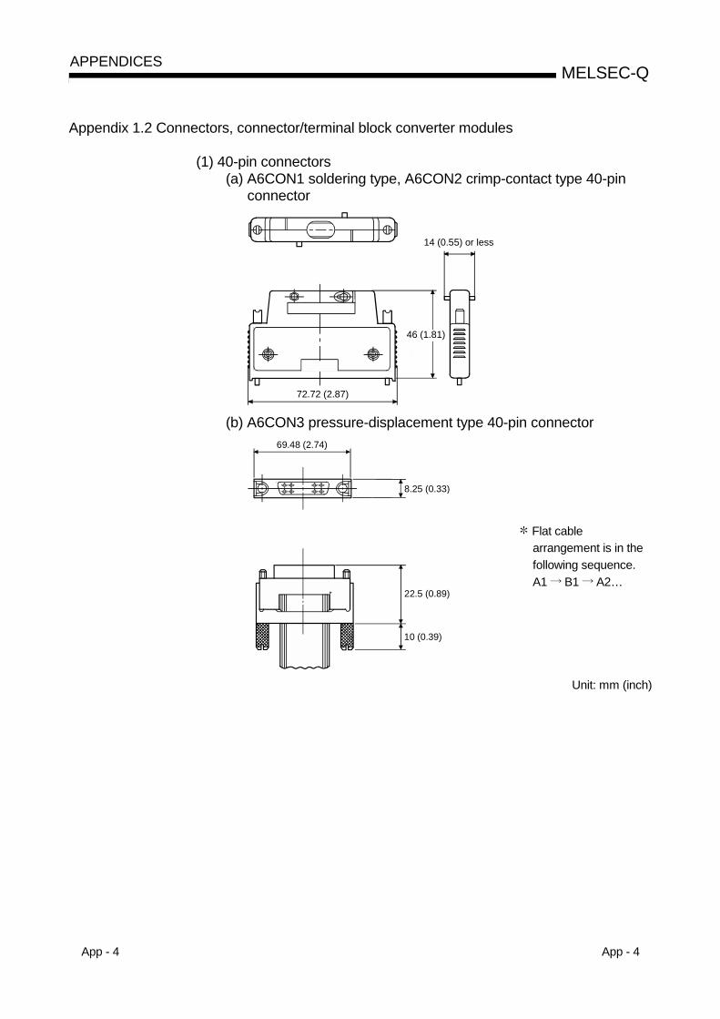
App - 4 App - 4
MELSEC-Q APPENDICES
Appendix 1.2 Connectors, connector/terminal block converter modules
(1) 40-pin connectors (a) A6CON1 soldering type, A6CON2 crimp-contact type 40-pin
connector
72.72 (2.87)
46 (1.81)
14 (0.55) or less
(b) A6CON3 pressure-displacement type 40-pin connector
69.48 (2.74)
8.25 (0.33)
22.5 (0.89)
10 (0.39)
Flat cable arrangement is in the following sequence. A1 B1 A2…
Unit: mm (inch)

App - 5 App - 5
MELSEC-Q APPENDICES
(2) 37-pin D-sub connectors
(a) A6CON1E soldering type, A6CON2E crimp-contact type 37-pin D-sub connector
46 (1
.81)
69.5 (2.74)
20.3(0.8)
(b) A6CON3E pressure-displacement type 37-pin D-sub connector
3.4 (0.13)
5.9 (0.23)
69.4 (2.73)
12.6 (0.5)
Unit: mm (inch)

App - 6 App - 6
MELSEC-Q APPENDICES
(3) A6TB 36 connector/terminal block converter module
89.6 (3.53)120 (4.73)
48 (1.89)52 (2.05)
5.5 (0.22)
17.3
(0.6
8)44
(1.7
3)
78.5
(3.0
9)
2 (0.08)- 4.5 (0.18) mounting hole(M4 25)
(4) A6TB 54 connector/terminal block converter module
48 (1.89)52 (2.05)
124.6 (4.91)155 (6.11)
5.5 (0.22)
17.3
(0.6
8)44
(1.7
3)
78.5
(3.0
9)
2 (0.08)- 4.5 (0.18) mounting hole(M4 25)
(5) A6TBX70 connector/terminal block converter module
48 (1.89)52 (2.05)
159.6 (6.29)190 (7.49)
5.5 (0.22)
17.3
(0.6
8)44
(1.7
3)
78.5
(3.0
9)
2 (0.08)- 4.5 (0.18) mounting hole(M4 25)
Unit: mm (inch)

App - 7 App - 7
MELSEC-Q APPENDICES
Appendix 1.3 Spring Clamp Terminal Block
(1) Q6TE-18S Installed on a module (Example: QX10)
17
15
13
11
9
7
5
3
1
18
16
14
12
10
8
6
4
2
Q6TE -18S
27(1.06)
7.62
(0.3
0)82.5
(3.2
5)
23(0.91)
90*(3.54)
Unit: mm(inch) *: The depth of the module installed with a Q6TE-18S is equivalent with the factory default dimensions for that
module.

App - 8 App - 8
MELSEC-Q APPENDICES
Appendix 2 Compatibility with MELSEC-AnS Series I/O modules
Note that the MELSEC-Q series I/O modules and MELSEC-AnS series I/O modules are different in external terminal block configuration. Differences in terminal block configuration are indicated below.
(1) Input modules
Terminal Block Number
QX10, QX40 QX80 A1SX10, A1SX40,
A1SX80
TB9 X08 X08 COM TB10 X09 X09 X08 TB11 X0A X0A X09
• • •
• • •
• • •
• • •
TB16 X0F X0F X0E TB17 COM NC X0F TB18 NC COM COM TB19 — — Vacant TB20 — — Vacant
(2) Output modules Terminal
Block Number
QY10 QY40P A1SY10 A1SY40
TB9 Y08 Y08 COM1 12/24VDC TB10 Y09 Y09 Y08 COM1 TB11 Y0A Y0A Y09 Y08
• • •
• • •
• • •
• • •
• • •
TB16 Y0F Y0F Y0E Y0D TB17 COM 12/24VDC Y0F Y0E TB18 NC COM COM2 Y0F TB19 — — 24VDC 12/24VDC TB20 — — 0V COM2

App - 9 App - 9
MELSEC-Q APPENDICES
Terminal
Block Number
QY50 A1SY50 Terminal
Block Number
QY80 A1SY80
TB9 Y08 12/24VDC TB9 Y08 COM1 TB10 Y09 COM1 TB10 Y09 0V TB11 Y0A Y08 TB11 Y0A Y08
• • •
• • •
• • •
• • •
• • •
• • •
TB16 Y0F Y0D TB16 Y0F Y0D TB17 12/24VDC Y0E TB17 COM Y0E TB18 COM Y0F TB18 0V Y0F TB19 — 12/24VDC TB19 — COM2 TB20 — COM2 TB20 — 0V
POINT
The 40-pin connector used with the MELSEC-AnS series I/O module can be used intact with the MELSEC-Q series I/O module. The 37-pin D-sub connector used with the MELSEC-AnS series I/O module is the same in wiring as, but opposite in cable pulling direction to, the MELSEC-Q series I/O module. (The conventional cable for A6TB cannot be used.)
WARRANTY
Please confirm the following product warranty details before starting use. 1. Gratis Warranty Term and Gratis Warranty Range
If any faults or defects (hereinafter "Failure") found to be the responsibility of Mitsubishi occurs during use of the product within the gratis warranty term, the product shall be repaired at no cost via the dealer or Mitsubishi Service Company. Note that if repairs are required at a site overseas, on a detached island or remote place, expenses to dispatch an engineer shall be charged for. [Gratis Warranty Term]
The gratis warranty term of the product shall be for one year after the date of purchase or delivery to a designated place. Note that after manufacture and shipment from Mitsubishi, the maximum distribution period shall be six (6) months, and the longest gratis warranty term after manufacturing shall be eighteen (18) months. The gratis warranty term of repair parts shall not exceed the gratis warranty term before repairs.
[Gratis Warranty Range] (1) The range shall be limited to normal use within the usage state, usage methods and usage environment, etc.,
which follow the conditions and precautions, etc., given in the instruction manual, user's manual and caution labels on the product.
(2) Even within the gratis warranty term, repairs shall be charged for in the following cases. 1. Failure occurring from inappropriate storage or handling, carelessness or negligence by the user. Failure caused
by the user's hardware or software design. 2. Failure caused by unapproved modifications, etc., to the product by the user. 3. When the Mitsubishi product is assembled into a user's device, Failure that could have been avoided if functions
or structures, judged as necessary in the legal safety measures the user's device is subject to or as necessary by industry standards, had been provided.
4. Failure that could have been avoided if consumable parts (battery, backlight, fuse, etc.) designated in the instruction manual had been correctly serviced or replaced.
5. Failure caused by external irresistible forces such as fires or abnormal voltages, and Failure caused by force majeure such as earthquakes, lightning, wind and water damage.
6. Failure caused by reasons unpredictable by scientific technology standards at time of shipment from Mitsubishi. 7. Any other failure found not to be the responsibility of Mitsubishi or the user.
2. Onerous repair term after discontinuation of production
(1) Mitsubishi shall accept onerous product repairs for seven (7) years after production of the product is discontinued. Discontinuation of production shall be notified with Mitsubishi Technical Bulletins, etc.
(2) Product supply (including repair parts) is not possible after production is discontinued. 3. Overseas service
Overseas, repairs shall be accepted by Mitsubishi's local overseas FA Center. Note that the repair conditions at each FA Center may differ.
4. Exclusion of chance loss and secondary loss from warranty liability
Regardless of the gratis warranty term, Mitsubishi shall not be liable for compensation to damages caused by any cause found not to be the responsibility of Mitsubishi, chance losses, lost profits incurred to the user by Failures of Mitsubishi products, damages and secondary damages caused from special reasons regardless of Mitsubishi's expectations, compensation for accidents, and compensation for damages to products other than Mitsubishi products and other duties.
5. Changes in product specifications
The specifications given in the catalogs, manuals or technical documents are subject to change without prior notice. 6. Product application
(1) In using the Mitsubishi MELSEC programmable logic controller, the usage conditions shall be that the application will not lead to a major accident even if any problem or fault should occur in the programmable logic controller device, and that backup and fail-safe functions are systematically provided outside of the device for any problem or fault.
(2) The Mitsubishi general-purpose programmable logic controller has been designed and manufactured for applications in general industries, etc. Thus, applications in which the public could be affected such as in nuclear power plants and other power plants operated by respective power companies, and applications in which a special quality assurance system is required, such as for Railway companies or National Defense purposes shall be excluded from the programmable logic controller applications. Note that even with these applications, if the user approves that the application is to be limited and a special quality is not required, application shall be possible. When considering use in aircraft, medical applications, railways, incineration and fuel devices, manned transport devices, equipment for recreation and amusement, and safety devices, in which human life or assets could be greatly affected and for which a particularly high reliability is required in terms of safety and control system, please consult with Mitsubishi and discuss the required specifications.

User's Manual User's Manual
Mitsubishi Programmable Logic Controller
MODEL
MODELCODE
Q-IO-U-E
13JL99
SH(NA)-080042-L(0305)MEE
I/O Module Type Building BlockI/O Module Type Building Block
B
Specifications subject to change without notice.
When exported from Japan, this manual does not require application to theMinistry of Economy, Trade and Industry for service transaction permission.
HEAD OFFICE : 1-8-12, OFFICE TOWER Z 14F HARUMI CHUO-KU 104-6212,JAPANNAGOYA WORKS : 1-14 , YADA-MINAMI 5-CHOME , HIGASHI-KU, NAGOYA , JAPAN