
Modeling GaAs PIN diodes for microwave and Millimeter Wave Applications (1)
6
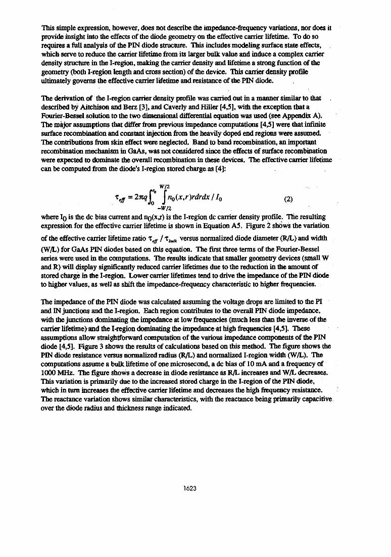
MODELING GAAs PIN DIODES FOR MICROWAVE AND MILLIMETER WAVE APPLICATIONS Robert H. Caverly Nitin Department of Electrical and Corporate Research and Development Computer Engineering M/A-COM, Inc. Univ. Massachusetts Dartmouth 100 Chelmiford Street North Dartmouth, MA USA 02747 Lowell, MA USA 01853 Abstract The need to keep system development cost low has given important emphasis to using well-defined solid-state component models in design and simulation of systems. This paper presents a new model for predicting the impedance of monolithic GaAs PIN diodes at microwave and millimeter wave frequencies. Introduction The market for microwave and millimeter wave systems for applications such as IVHS and PCN has increased the need for low cost, high frequency solid-state components. Ihe need to keep system development cost low in this competitive environment has given important emphasis to using well-defined solid-state component models in design and simulation of systems prior to fabrication and production. GaAs PIN diodes are one of a number of devices used extensively in these products. Microwave and millimeter wave applications usually require that GaAs PIN diodes be of small geometry, typically tens of microns i diameter and I-region thicknesses of only a few microns. A study was undertaken to identify the factors influencing GaAs PIN diode impedance because a senes of fabricated devices exhibited variations in forward bias impedance as a function of frequency (out to beyond X-band) and diode diameter (see Figure 1). This study focused on modeling not only the impedance versus frequency response, but also the observed dependence of the diode impedance on device geometry. A result of this effort was the development of an efficient method to predict the frequency and geometry dependence of the impedance of GaAs PIN diodes. The models were verified experimentally. Diameter-Dependence on GaAs PIN Diode Impedance The classical expression for the high frequency PIN diode resistance shows that this resistance is inversely proportional to the I-region effective carrier lifetime (ff) [1]: &S =-W 2pI0-r (1) 1622
Transcript of Modeling GaAs PIN diodes for microwave and Millimeter Wave Applications (1)

MODELING GAAs PIN DIODES FOR MICROWAVEAND MILLIMETER WAVE APPLICATIONS
Robert H. Caverly NitinDepartment of Electrical and Corporate Research and Development
Computer Engineering M/A-COM, Inc.Univ. Massachusetts Dartmouth 100 Chelmiford StreetNorth Dartmouth, MA USA 02747 Lowell, MA USA 01853
Abstract
The need to keep system development cost low has given important emphasis to using well-definedsolid-state component models in design and simulation of systems. This paper presents a newmodel for predicting the impedance of monolithic GaAs PIN diodes at microwave and millimeterwave frequencies.
Introduction
The market for microwave and millimeter wave systems for applications such as IVHS and PCNhas increased the need for low cost, high frequency solid-state components. Ihe need to keepsystem development cost low in this competitive environment has given important emphasis tousing well-defined solid-state component models in design and simulation of systems prior tofabrication and production. GaAs PIN diodes are one of a number of devices used extensively inthese products.
Microwave and millimeter wave applications usually require that GaAs PIN diodes be of smallgeometry, typically tens of microns i diameter and I-region thicknesses of only a few microns. Astudy was undertaken to identify the factors influencing GaAs PIN diode impedance because asenes of fabricated devices exhibited variations in forward bias impedance as a function offrequency (out to beyond X-band) and diode diameter (see Figure 1). This study focused onmodeling not only the impedance versus frequency response, but also the observed dependence ofthe diode impedance on device geometry. A result of this effort was the development of an efficientmethod to predict the frequency and geometry dependence of the impedance ofGaAs PIN diodes.The models were verified experimentally.
Diameter-Dependence on GaAs PIN Diode Impedance
The classical expression for the high frequency PIN diode resistance shows that this resistance isinversely proportional to the I-region effective carrier lifetime (ff) [1]:
&S =-W 2pI0-r (1)
1622
Ibis simple expression, however, does not describe the impedance-frequency variations, nor does itprovide insight into the effects of the diode geometry on the effective carrier lifetime. To do sorequires a full analysis of the PIN diode struct. This includes modeling surface state effects,which serve to reduce the carrier lifetime from its larger bulk value and induce a,complex carierdensity structure in the I-region, making the carrier density and lifetime a- stong function of thegeometry (both I-region length and-cross section) of the device. This cafrier density profileultimately governs the effective carrier lifetime and resistance of the PIN diode.
The derivation of the I-region carder density profile was caried out in a manner similar to tdescribed- by Aitchison and Berz [3], and Caverly and Hiller [4,5], with the exception that aFourier-Bessel solution to the two dimensional differential equation was used (see Appendix A).The major assumptions that differ fo previous pedance computations [4,5] were that ininitesurface recombination and constant injection from the heavily doped end regions were assumed.The contributions from skin effect were neglected. Band to band recombination, an mportantrecombination mechanism in GaAs, was not considered since the effects of surface recombinationwere expected to dominate the overall recombination in these devices. The effective carier lifetmecan be computed from the diode's I-region stored charge as [41:
W/2
hif =2cqJ ,fno(x r)rdrdx/Io (2)-W/2
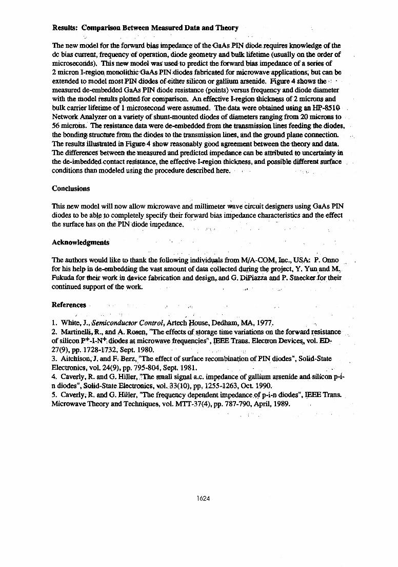
whee Io is the dc bias current and no-(x,r) is the I-region dc carrier density profile. The resultingexpression for the effective carrier lifetime is shown in Equation AS. Figure 2 shows the variation
of the effective cardier lifetime ratio 'c, / tb4lk versus normalized diode diameter (RAL) and width(W/L) for GaAs PIN diodes based on this equation. The first three terms of the Fourier-Besselseries were used in the computations. The results indicate that smaller geometry devices (smallWand R) will display significantly reduced carrier lifetimes due to the reduction in the amount ofstored charge in the I-region. Lower carrier lifetimes tend to drive the impedance of the PIN diodeto higher values, as well as shift the impedance-frequency characteristic to higher frequencies.
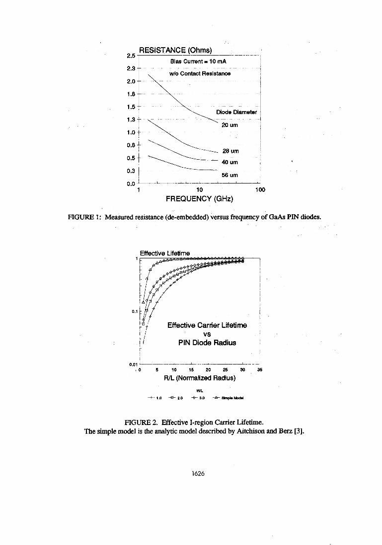
The impedance of the PIN diode was calculated ass g the voltage drops are limited to the PIand IN junctions and the I-region. Each region contributes to the overall PIN diode impedance,with the junctions dominatig he impedance at low frequencies (much less than t veerse of thecarrier lifetime) and the I-region dominating the,impedance at high frequencies [4,5]. Theseassumptions allow straitorward computation of the various impedance components of the PINdiode [4,5]. Figure 3 shows the results of calculations based on this method. The figure shows thePIN diode resistance versus normalized radiW (R/L) and normalized I-region width (W/L). Thecomputations assune a bulk lifetime of one microsecond, a dc bias of 10 mA and a frequency of1000 MHz. The figure shows a decrease in diode resistance As R/L increases-and W/L decreases.This variation is primarily due to the increased stored charge mi the I-region of the PIN diode,which in turn increases the effective cafrier lifetime and decreases the high frequency-resistance.The reactance variadon shows similar characteristics, with the reactance being prmarily capacifiveover the diode radius and thickness rmnge indicated.
1623
Results: Comparison Between Measured Data and Theory
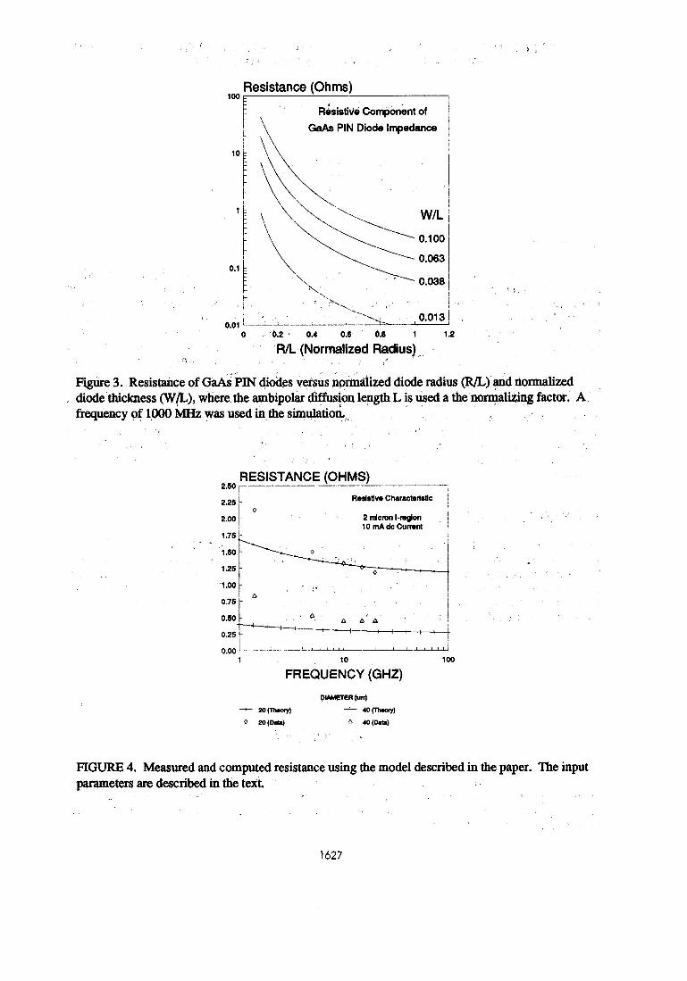
The new model for the forward bias impedance of the(laAs PIN diode requires knowledge of thedc bias current, frequency of operation, diode geometry and bulk lifetime (usually on the order ofmicroseconds). This new model was used to predict the forward bias impedance of a series of2 micron I-region monolithic GaAs PIN diodes fabricated for microwave- applications; but can beextended to model most PIN diodes ofeither silicon or gallium arsenide. Figure 4 shows themeasured de-embedded GaAs PIN diode resistance (points) versus frequency and diode diameterwith the model tesults plotted for comparison. An effective I-region thickness of 2 microns adbulk carrier lifetime of 1 microsecond were assumed. The data were obtained using an BH-8510Network Analyzer on a variety of shunt-mounted diodes of diameters ranging from 20 microns to56 microns. The resistae data were de-embedded from the tansmission lines feeding the diodes,the bondingstructure fromithe diodes to the tramnsmission lines, and the ground plane connection.The results illustrated in Figure 4 show reasonably good agreement between the-theory and data.The differences between the measured ad predicted.impedance can be attributed to uncertainty inthe de-imbedded-contact resistance, the effective bI-region thickness, and possible different surfaceconditions than modeled using the procedure described here.
Conclusions
This new model will now allow microwave and millimeter wave circuit designers using GaAs PINdiodes to be able to completely specify their forward bias impedance characteristics and the effectthe surface has on the PIN diode impedance.
Acknowledgments
The authors would like to thank the following individuals from M/A-CQM, Ilc., USA: P. Onnofor his help in de-embedding the vast amount of data collected during the project, Y. Yun and M..Fukuda for their work in dvice fabrication and design, and G. DiPiazza and P. Staeckertfor theircontinued support of the work;
References
1. White, J.o Semiconductor Control, Artech flouse, Dedham, MA, 1977.2. MartinelliR., and A. Rosn, "1The effes of storage time variains on the forward resistanceof silicon P+-I-NNt diodes at microwave frequencies", WEE, Trans. Electron Device$s, vol. ED-27(9), pp. 1728-1732, Sept. 1980.3. Aitchison, J. and F. Berz,,"The effect of surface recombination of PI diodes", Solid-StateElectronics, vol. 24(9), pp. 795-804, Sept. 1981.4. Caverly, R. and G. Hiller, ."The smal signal a.c. impedace of gallium arsenide and silicon p--n diodes", Solid-State Electronics vol.. 33(10), pp., 12554263, Oct. 1990.5. Caverly, R. and G. Hiller, "The. frequency dependent impedance,of p-i-n diodes", EE Trans.Microwave Teory and Techniques, vol. MTT-37(4), pp. 787-790, April. 1989.
1624

Appendix A
An analysis using the basic semiconductor equations was applied to the PIN diode. Thedifferential equation is based on a cylindrical coordinate system and is shown in Equation Al:
an(x,r) n(x,r) a2n(x,r) a( an(x,r)at tbuk ax r ar ar 3 * (A)
The symbols have their usual peanings. A solution based on the Fourier-Bessel series was used,with boundary conditions consisting of infinite surface recombination and constant currentinjection across the diode cross section at each heavily doped end region. The resulting form forthe I-region carrier density can be written as:
nl (x, r) = , AmJo(zmr / rO )[Dpfcosh(YZ) + DE cosh( 32x (A)m=1
where the subscript of nj indicates either dc (no) or ac (nl) conditions,
2m=l+( )2 9 am= r, LV=DV§bilk (the ambipolar diffusion length), DA is theml+(Lo9rambipolar diffusion constant, ro is the radius of the PIN diode, the zm are the mth zeroes of thezeroth order Bessel function [JO(r)], and the Am are defmed by
Am =-2n
Jl(zm)[D +DPcosh(W/ym)L (A3)
The parameter nj is computed by integrating the current density over the diode cross section usingthe following relationship [3]:
r an(x,r)I, = 4cqDn J a IX=W/2rdr (A4)
where the subscript of II indicates either dc (To) or ac (I1) conditions. Equations Al through A4substituted into Equation 2 yield an expression that relates carrier lifetime to bulk lifetime, I-regionthickness (W) and diode radius (ro):
It ' sifnh(W /TYm) ismnh(W / Ym) l+(Lam)2'b,dk t=1 Z 1 + (Lam)2 (Dn + DPcosh(W / m)) m)) ()
1625
RESISTANCE (Ohms) _ _2.57
I Blas Current= 10 mA2.31-
I w/o Contact Resistance2.0 ..
.8 .. ---
1.8\5
Diode Diameter1.3+
20 um1.0+
0.8+ \ 2Bu\ -^- ~~28um
0.5t Or~~~~~40 um0.3 - -- -0.3 56 um0.0 -- WI,.
1 10 100FREQUENCY (GHz)
FIGURE 1: Measured resistance (de-embedded) versus frequency of GaAs PIN diodes.
Effective Lifetime
H / Effective Carder LifetimeL-l vsV| P|PIN Diode Radius
0.010 6 10 15 20 25 30 35
R/L (Normalized Radius)W/L
- 1.0 2.0 -4- 3.0 -8mpbI Mod
FIGURE 2. Effective I-region Carrier Lifetime.The simple model is the analytic model described by Aitchison and Berz [3].
1626
Resistance (Ohms)ResistiV4
GaAs PIN
10 \
0.1\
0.01 ~ \^
0 6.2 0.4 0.6
R/L (Normalizi
;e'Component ofDiode Impedancoe
I
W/L0.1000.063
0.038s ~~I
I.
;0.0130.8 1 1.2
ed Radius)
Figure 3. Resistance of GaAs PIN diodes versus nprmaiized diode radius (RJL) and dormalizeddiode thickness (W(L), where the ambipolar diffusion length L is used a the normalizing factor. Afrequency of 1000 MHz was used in the simulation,.
RESISTANCE (OHMS)2.60L _ --
2.6 Resisfive Charactedtefc2.00
1.76
1.60
1.25
1.00
0.75
0- ~~~~~~~~~~~~~~~~~~~2rMoron l-roon
10 mA dc Cuffet
,
0.60 lA aA
0.25
0.00 i LJ-J- I 1 .U II. _ _t W10 100
FREQUENCY (GHZ)pDIAMER (uni)
- 20 (Thory 40(rhoy0 20 (Dda) 6 40 (Dat)
FIGURE 4. Measured and computed resistance using the model descnrbed in the paper. The inputparameters are described in the text.
1627
1


