Modeling, Control and Design Considerations for … · MMC is proposed for use in the design of the...
188
Modeling, Control and Design Considerations for Modular Multilevel Converters Vahid Najmi Thesis submitted to the faculty of the Virginia Polytechnic Institute and State University in partial fulfillment of the requirements for the degree of Master of Science In Electrical Engineering Rolando Burgos, Chair Dushan Boroyevich Jih-Sheng Lai May 1 st , 2015 Blacksburg, VA Keywords: Modular Multilevel Converter (MMC), Alternate Arm Converter (AAC), DC Fault ride-through, Reliability-Oriented Design, Circulating Current Suppressing Control (CCSC), Capacitor Voltage Balance, Three- Phase Average Modeling, D-Q axis Modeling Copyright © 2015 Vahid Najmi
Transcript of Modeling, Control and Design Considerations for … · MMC is proposed for use in the design of the...

Modeling, Control and Design Considerations for Modular Multilevel Converters
Vahid Najmi
Thesis submitted to the faculty of the Virginia Polytechnic Institute and State University
in partial fulfillment of the requirements for the degree of
Master of Science
In
Electrical Engineering
Rolando Burgos, Chair
Dushan Boroyevich
Jih-Sheng Lai
May 1st, 2015
Blacksburg, VA
Keywords: Modular Multilevel Converter (MMC), Alternate Arm Converter (AAC), DC
Fault ride-through, Reliability-Oriented Design, Circulating Current Suppressing Control
(CCSC), Capacitor Voltage Balance, Three- Phase Average Modeling, D-Q axis
Modeling
Copyright © 2015 Vahid Najmi
Modeling, Control and Design Considerations for Modular
Multilevel Converters
Vahid Najmi
ABSTRACT
This thesis provides insight into state-of-the-art Modular Multilevel Converters
(MMC) for medium and high voltage applications. Modular Multilevel Converters have
increased in interest in many industrial applications, as they offer the following
advantages: modularity, scalability, reliability, distributed location of capacitors, etc. In
this study, the modeling, control and design considerations of modular based multilevel
converters, with an emphasis on the reliability of the converter, is carried out. Both
modular multilevel converters with half-bridge and full-bridge sub-modules are evaluated
in order to provide a complete analysis of the converter. From among the family of
modular based hybrid multilevel converters, the newly released Alternate Arm Converter
(AAC) is considered for further assessment in this study. Thus, the modular multilevel
converter with half-bridge and full-bridge power cells and the Alternate Arm Converter
as a commercialized hybrid structure of this family are the main areas of study in this
thesis. Finally, the DC fault analysis as one of the main issues related to conventional
VSC converters is assessed for Modular Multilevel Converters (MMC) and the DC fault
ride-through capability and DC fault current blocking ability is illustrated in both the
Modular Multilevel Converter with Full-Bridge (FB) power cells and in the Alternate

iii
Arm Converter (AAC). Accordingly, the DC fault control scheme employed in the
converter and the operation of the converter under the fault control scheme are explained.
The main contributions of this study are as follows: The new D-Q model for the
MMC is proposed for use in the design of the inner and outer loop control. The extended
control scheme from the modular multilevel converter is employed to control the
Alternate Arm Converters. A practical reliability-oriented sub-module capacitor bank
design is described based on different reliability modeling tools. A Zero Current
Switching (ZCS) scheme of the Alternate Arm Converter is presented in order to reduce
the switching losses of the Director Switches (DS) and, accordingly, to implement the
ZCS, a design procedure for the Arm inductor in the AAC is proposed. The capacitor
voltage waveform is extracted analytically in different load power factors and the
waveforms are verified by simulation results. A reliability-oriented switching frequency
analysis for the modular multilevel converters is carried out to evaluate the effect of the
switching frequency on the MMC’s operation. For the latter, a DC fault analysis for the
MMC with Full-Bridge (FB) power cells and the AAC is performed and a DC fault
control scheme is employed to provide the capacitor voltage control and DC fault current
limit, and is illustrated herein.

iv
Acknowledgements
First and foremost, I would like to thank my supervisor, Dr. Rolando Burgos, for
offering me the opportunity to pursue my education at the Center for Power Electronics
Systems (CPES), Virginia Tech. I have learned a lot from him and from CPES. His
guidance, constructive comments, insightful discussions and generous support have
allowed me to successfully finish my MS thesis; I sincerely appreciate all of the
contributions of time, ideas and funding he provided throughout my MS work. I would
also like to thank Professor Dushan Boroyevich for sharing his experience and
knowledge with me, and for his fruitful discussions, friendly advice and thoughtful
comments. I am grateful for my friends and colleagues in the department, in particular
Jun Wang and Mohammad Nawaf Nazir, for their contributions and support. All photos,
screenshots, and figures used have been created by the author for this thesis. I would also
like to thank ABB, for funding of this work.
Finally, I would like to thank my family, especially my loving mom and my
siblings, in particular my sister Bita, for their kindness and encouragement along my way.
I am grateful to have them in my life.
v
Table of Contents
CHAPTER 1 INTRODUCTION................................................................................ 1
1.1 Motivation and Application Background .............................................................. 1
1.2 Topology Evaluations .............................................................................................. 4
1.3 Hybrid Modular Multilevel Converters................................................................. 7
1.3.1 Hybrid Converter with a Waveshaping Circuit on the AC Side ....................... 7
1.3.2 Hybrid Converter with a Waveshaping Circuit on the DC Side ....................... 8
1.3.3 Alternate-Arm Converter (AAC), Hybrid Converter with Wave-Shaping
Circuit on DC side ................................................................................................... 11
1.3.4 VSC-HVDC Using Multilevel Technology Review ....................................... 12
1.4 Research Objectives ............................................................................................... 14
1.5 Thesis Organization ............................................................................................... 16
CHAPTER 2 MODULAR MULTILEVEL CONVERTERS MODELING ........ 18
2.1 Introduction ............................................................................................................ 18
2.2 Modular Multilevel Converter Modeling (MMC) .............................................. 21
2.2.1 MMC Switching Model .................................................................................. 21
2.2.2 Steady-State Harmonic Analyisis of the MMC .............................................. 25
2.2.3 Average Model of the MMC........................................................................... 27

vi
2.2.4 D-Q Model of the MMC ................................................................................. 33
2.2.5 Simulation Results .......................................................................................... 38
2.2 Alternate-Arm Converter Modeling .................................................................... 43
2.3.1 Introduction ..................................................................................................... 43
2.3.2 Alternate Arm Converter (AAC) Operation Principles .................................. 44
2.3.3 AAC Voltage and Current Specifications ....................................................... 46
2.3.4 Sweet Spot Calculation of the AAC ............................................................... 47
2.3.5 AAC Switching Modeling ............................................................................. 49
2.3 Conclusion .............................................................................................................. 53
CHAPTER 3 MODULAR MULTILEVEL CONVERTERS CONTROL .......... 56
3.1 Introduction ............................................................................................................... 56
3.2 Closed Loop Control of the MMC ........................................................................ 61
3.2.1 Design of the Circulating Current Suppressing PR Controller ....................... 61
3.2.2 Closed Loop Output Current Control of the MMC ........................................ 66
3.3 Closed-Loop Control of the AAC ......................................................................... 67
3.3.1 Capacitor Voltage Analysis of each Module in the AAC ............................... 68
3.3.2 Capacitor Voltage Balance Control and Energy Balance Control Schemes ... 70
3.3.3 Overlap Time Control of the AAC ................................................................. 70
3.3.4 Individual Capacitor Voltage Control of the AAC ......................................... 72
3.2.5 Closed-loop Output Current control of the AAC ............................................ 72

vii
3.4 Conclusion .............................................................................................................. 73
CHAPTER 4 MODULAR MULTILEVEL CONVERTERS DESIGN
CONSIDERATIONS ...................................................................................................... 74
4.1 Introduction ............................................................................................................ 74
4.2 High Reliability Capacitor Bank Design for Modular Multilevel Converters . 75
4.2.1 Capacitor Bank Size Design in Modular Multilevel Converter ...................... 77
4.2.2 Simulation Analysis to Evaluate Reliability of CB ........................................ 79
4.2.3 Case Study for Capacitor Bank Design .......................................................... 80
4.2.4 Power Loss, Hot Spot, Failure Rate and Reliability Calculations of the
Capacitor Bank......................................................................................................... 83
4.2.5 Comparison Among Reliability of Each Case ................................................ 85
4.2.6 Difference Between Reliability of the Internally Parallel Connected and Non-
Connected Capacitor Bank Considering Failure Mode Of the Capacitor................ 85
4.2.7 Enhancement of the Reliability of the ALE Capacitor Bank by Adding Film
Capacitor .................................................................................................................. 87
4.3 Reliability Modeling of the Capacitor Bank for MMC Using Markov State-Space
Model ................................................................................................................................ 88
4.3.1 Markov State-Space Model ............................................................................. 91
4.3.2 Comparison with Three-Reliability Models ................................................... 97
4.3.3 Conclusion ...................................................................................................... 98

viii
4.4 Modulation Techniques’ Influence on the Cap Voltage and Arm Current Ripple
........................................................................................................................................... 98
4.5 Design of the L and C with Circulating Current Controller .............................. 100
4.6 Reliability-Oriented Switching Frequency Analysis for the Modular Multilevel
Converter (MMC) ......................................................................................................... 101
4.6.1 Harmonic Components Analysis of MMC for Low Switching Frequency
Applications ........................................................................................................... 101
4.6.2 Power Loss Calculation of the MMC With and Without Circulating Current
Suppressing Control ............................................................................................... 105
4.6.3 Reliability Modeling of the MMC Based on the Markov-State Space Model
................................................................................................................................ 107
4.6.4 Reliability Comparison of MMC Under Different Frequencies With and
Without Circulating Current Controller ................................................................. 110
4.6.5 Conclusions ................................................................................................... 111
4.7 AAC Design Considerations................................................................................... 111
4.7.1 Number of Cells in the AAC ........................................................................ 111
4.7.2 Number of Director Switches in the AAC .................................................... 112
4.7.3 DC- Fault Management and Ride-Through of the AAC .............................. 113
4.7.4 Zero Current Switching (ZCS) Operation of the Director Switches in RL loads
................................................................................................................................ 114
4.7.5 Simulation Analysis ...................................................................................... 120

ix
4.8 Design and Switching Losses Comparison Between AAC and MMC ............... 128
4.9 Conclusions .............................................................................................................. 130
CHAPTER 5 DC FAULT RIDE-THROUGH CAPABILITY OF MODULAR
MULTILEVEL CONVERTERS ................................................................................. 132
5.1 Motivation ............................................................................................................. 132
5.2 Introduction ............................................................................................................. 133
5.3 DC Fault Analysis of MMC Full-Bridge and AAC.............................................. 136
5.3.1 During Fault Detection Time (t0 to t1) .......................................................... 139
5.3.2 During IGBT’s Turned-off Time in Which Fault Currents Flow Through
Diodes (t1 to t2)....................................................................................................... 140
5.3.3 During Fault Currents’ Flow Through Diodes and the Fault Current Blocking
Time (t2 to t3) ......................................................................................................... 141
5.4 DC Fault Closed Loop Control Strategy of MMC Full-Bridge and AAC ......... 142
5.5 Simulation Result .................................................................................................... 144
5.5.1 DC Fault Simulation With Rsc 10 Ω for MMC-FB ..................................... 146
5.5.2 DC Fault Simulation With Rsc 0.01 Ω for MMC-FB .................................. 146
5.5.3 DC Fault Simulation With Rsc 0.01 Ω for AAC .......................................... 147
5.5.4 DC Fault Interrupt Simulation With Rsc 0.01 Ω for MMC- FB .................. 149
5.6 Conclusions .............................................................................................................. 151
x
CHAPTER 6 SUMMARY, CONCLUSIONS AND FUTURE WORK .............. 152
6.1 Summary ............................................................................................................... 152
6.2 Conclusions ........................................................................................................... 153
6.3 Future Work ......................................................................................................... 155
References ...................................................................................................................... 157

xi
List of Figures
Figure 1- 1: Applications of Multilevel Converters ............................................................ 2
Figure 1- 2: Multilevel Converters’ classifications ............................................................ 3
Figure 1- 3: Modular Multilevel Converter conceptual realization .................................... 5
Figure 1- 4: Voltage waveform in the two-level voltage source and Modular Multilevel
Converter............................................................................................................................. 5
Figure 1- 5: Building blocks for the MMC that have been commercialized so far ............ 6
Figure 1- 6: Hybrid Voltage Source Multilevel Converter with Wave-shaping circuit on
the AC side .......................................................................................................................... 8
Figure 1- 7: H-bridge converter with Active DC Capacitor and wave-shaping circuit on
the DC side .......................................................................................................................... 9
Figure 1- 8: Hybrid Converter with Wave-Shaping circuit in parallel with H-Bridges ... 10
Figure 1- 9: Alternate-Arm Converter: series of director switches with wave-shaping
circuit on the DC side ....................................................................................................... 11
Figure 1- 10: VSC HVDC multilevel technology review [23] Alstom Grid,
www.alstom.com/products-services/product-catalogue/electrical-grid-new/hvdc/hvdc-
solutions/hvdc-maxsinetm/, 2011, [37] Siemens, www.siemens.com/energy/hvdcplus,
2011 and [38] ABB, www.abb.com/hvdc, 2013. Used under fair use, 2015. .................. 13
Figure 1- 11: Modular Multilevel Converter manufacured by Alstom Grid, Siemens and
ABB, [23] Alstom Grid, www.alstom.com/products-services/product-
catalogue/electrical-grid-new/hvdc/hvdc-solutions/hvdc-maxsinetm/, 2011, [37] Siemens,
xii
www.siemens.com/energy/hvdcplus, 2011 and [38] ABB, www.abb.com/hvdc, 2013.
Used under fair use, 2015. ................................................................................................ 13
Figure 2- 1: Modular Multilevel Converter topology with each sub-module structure. ... 19
Figure 2- 2: Switching Model of the MMC. ..................................................................... 22
Figure 2- 3 (a) Switching model of MMC with one power cell in each arm, (b)
Circulating current switching model in the MMC ............................................................ 27
Figure 2- 4 abc Average Model for the MMC. ................................................................. 33
Figure 2- 5 D-Q Frame Model for the MMC. ................................................................... 37
Figure 2- 6: MMC Capacitor Voltage from Switching, abc and DQ model..................... 39
Figure 2- 7: DC Current from Switching, abc and DQ model .......................................... 40
Figure 2- 8: Phase current from switching, abc average and DQ model .......................... 40
Figure 2- 9: Circulating current from switching, abc average and DQ model ................. 41
Figure 2- 10: MMC DC, phase, and circulating current from switching, abc average and
DQ model .......................................................................................................................... 42
Figure 2- 11: Open loop transfer function of output current to duty cycle in DQ. ........... 42
Figure 2- 12: (a) Alternate Arm Converter (AAC), (b) Modular Multilevel Converter
(Half- Bridge).................................................................................................................... 43
Figure 2- 13: Basic operation of the AAC ........................................................................ 46
Figure 2- 14 Single phase AAC operation in positive and negative cycles ...................... 48
Figure 2- 15: AAC with one module in each arm ............................................................. 49
Figure 3- 1: Modular Multilevel Converter topology with each power module structure 58
Figure 3- 2: The capacitor average voltage balance control with circulating current
suppressing control ........................................................................................................... 62
xiii
Figure 3- 3: Individual cell capacitor voltage balance control ......................................... 63
Figure 3- 4: Bode plot of the circulating current suppressing Proportional Quasi Resonant
(PQR) controller................................................................................................................ 65
Figure 3- 5: Upper phase-arm current harmonic contents a) without the circulating current
suppressing controller b) with circulating current suppressing control ............................ 66
Figure 3- 6: Closed loop control of the MMC .................................................................. 67
Figure 3- 7: Capacitor Voltage Analysis of the AAC ....................................................... 68
Figure 3- 8: Capacitor voltage ripple in different load power factors .............................. 69
Figure 3- 9: The upper and lower arm references with Overlap ....................................... 71
Figure 3- 10: The overlap time control between upper and lower arm DS ...................... 71
Figure 3- 11: Individual capacitor voltage control ........................................................... 72
Figure 4- 1: Failure cause probability in power electronics systems ................................ 76
Figure 4- 2: The effect of ESR on each module capacitor voltage ................................... 80
Figure 4- 3: Current waveform through Capacitor and FFT analysis for each three-Case
a) Case 1, b) Case 2 and c) Case 3 .................................................................................... 82
Figure 4- 4: Three sample designs illustration for capacitor bank in case 1 C=3400uF (a)
CDE ALE Capacitor Bank Design, (b) CDE Film Capacitor Bank Design, (c)
Elecronicon Film Capacitor Bank Design ........................................................................ 83
Figure 4- 5: N series and M parallel capacitor bank ......................................................... 84
Figure 4- 6: Reliability function comparison among three different cases a) Case 1 b)
Case 2 and c) Case 3 ......................................................................................................... 85

xiv
Figure 4- 7: Two- Design of CB a) Internally Parallel Connected for open circuit
dominant failure mode b) not internally connected for the short circuit dominant failure
mode .................................................................................................................................. 86
Figure 4- 8: Reliability comparison for two- design approach of the Capacitor Bank (CB)
R1 with dominant short and R2 with dominant open failure mode .................................. 86
Figure 4- 9: Open circuit failure mode with adding fuses to the each capacitor branch .. 87
Figure 4- 10: (a) Hybrid Film and ALE capacitor bank for case 1, (b) Reliability
Comparison among the Hybrid Film and ALE capacitor bank in case 1 ......................... 87
Figure 4- 11: The current and voltage through the capacitor bank of one module ........... 89
Figure 4- 12: Markov State-Space Model of the three different design of capacitor bank,
(a) Film Electronicon (b) CDE ALE (c) CDE Film .......................................................... 90
Figure 4- 13: The Markov reliability model of the capacitor bank which is modeled in
Figure 4-12 (a) .................................................................................................................. 93
Figure 4- 14: The Markov reliability model of the capacitor bank which is modeled in
Figure 4-12 (b) .................................................................................................................. 93
Figure 4- 15: The Markov reliability model of the capacitor bank which is modeled in
Figure 4-12 (c) .................................................................................................................. 94
Figure 4- 16: The failure rate of the system extracted from Markov Model, (a) Film
Electronicon, (b) ALE CDE and (c) Film CDE ................................................................ 94
Figure 4- 17: The voltage variation over the capacitor bank in each module (a) for Film
Electronicon design Figure 4-12 (a). (b) For ALE CDE design Figure 4-12 (b). and (c) for
Film CDE design Figure 4-12 (c) ..................................................................................... 95

xv
Figure 4- 18: The different reliability modeling of the capacitor bank using part counts,
combinatorial and Markov model (a) for Film Electronic design Figure 4-12.a (b) For
ALE CDE design Figure 4-12.b and (c) for Film CDE design Figure 4-12.c .................. 96
Figure 4- 19: The switching ripple of the arm current and the capacitor voltage with
respect to the frequency .................................................................................................. 104
Figure 4- 20: Peak-to-peak voltage ripple of the capacitor and the output current total
harmonic distortion in the different frequency ranges .................................................... 107
Figure 4- 21: Switching losses of the IGBT in different frequencies, with and without
CCSC .............................................................................................................................. 107
Figure 4- 22: Reliability Model of the Modular Multilevel Converter with three-phase
output voltage, current, circulating current, upper arm, DC current and capacitor voltage
in each failure state ......................................................................................................... 109
Figure 4- 23: Markov Reliability Model of the MMC with Circulating Current
Suppressing Controller in different frequencies ............................................................. 110
Figure 4- 24: Voltage over the Director Switches in each cycle .................................... 113
Figure 4- 25: Three different scenarios of DC-fault ride-through of the AAC .............. 114
Figure 4- 26: Zero Current Switching realization in AAC vs. Hard Switching ............. 116
Figure 4- 27: Proposed overlap time scenario for the DS ............................................... 116
Figure 4- 28: The behavior of the AAC during the overlap time ................................... 117
Figure 4- 29: The equivalent circuit of the AAC during overlap ................................... 117
Figure 4- 30: Arm, DC and Phase Current and cap voltages .......................................... 121
Figure 4- 31: Capacitor voltage balance scheme ............................................................ 122
Figure 4- 32: Capacitor voltage waveform ..................................................................... 122

xvi
Figure 4- 33: Three-phase output current ....................................................................... 123
Figure 4- 34: Three Phase output line-to-line voltage .................................................... 123
Figure 4- 35: Three Phase output pole voltages .............................................................. 124
Figure 4- 36: Upper Arm DS voltage and current .......................................................... 124
Figure 4- 37: DS voltage and current .............................................................................. 125
Figure 4- 38: Arm, DC and Phase Current and cap voltages .......................................... 125
Figure 4- 39: Capacitor voltage balance scheme ............................................................ 126
Figure 4- 40: Capacitor voltage waveform ..................................................................... 127
Figure 4- 41: Three Phase output line to line voltage ..................................................... 127
Figure 4- 42: Three-phase output current ....................................................................... 127
Figure 4- 43: AAC switching power losses .................................................................... 129
Figure 4- 44: MMC (half-bridge) switching power losses ............................................. 130
Figure 4- 45: MMC (Half Bridge) and AAC total switching losses ............................... 130
Figure 5- 1: DC Fault Occurrence in (a) Modular Multilevel Converter (MMC) with
Half-Bridge Power Cells (b) Modular Multilevel Converter (MMC) with Full-Bridge
Power Cells and (c) Alternate Arm Converter (AAC).................................................... 134
Figure 5- 2: (a) Simplified version of the Double-Clamp submodule (b) normal operation
T5 is on, (c) T5 is off during fault, current limiting in positive current direction and (d)
T5 is off during fault in negative current direction. ........................................................ 135
Figure 5- 3: A three- phase grid tied (a) MMC with Full-Bridge cell, (b) AAC ........... 137
Figure 5- 4: DC Fault path through the antiparallel diodes ............................................ 138
Figure 5- 5: DC Fault path at the final stage of fault clearance ...................................... 139
Figure 5- 6: the upper and lower arm current for Full-Bridge MMC and AAC ............. 142

xvii
Figure 5- 7: The closed-loop control of FB MMC and AAC during the DC Fault ........ 143
Figure 5- 8: DC Fault scenario for Full-Bridge MMC and AAC ................................... 145
Figure 5- 9: DC Fault simulation under Rsc 10 Ω for MMC-FB ................................... 145
Figure 5- 10: DC Fault simulation under Rsc 0.01 Ω for MMC-FB .............................. 147
Figure 5- 11: DC Fault simulation under Rsc 0.01 Ω for AAC ...................................... 148
Figure 5- 12: DC Fault interruption simulation under Rsc 0.01 Ω for MMC-FB .......... 149
Figure 5- 13: DC Fault simulation under Rsc 0.01 Ω for MMC-FB .............................. 150
xviii
List of Tables
Table 2- 1: MMC parameters values for DQ model verification ...................................... 39
Table 3- 1: MMC parameters values for closed-loop control simulation ......................... 64
Table 3- 2: The CCSC controller parameters ................................................................... 64
Table 3- 3: Stress Analysis With/ Without Circulating Current Suppressing Controller . 66
Table 4- 1: Circuit Parameters value ................................................................................ 80
Table 4- 2: Three Capacitor bank Design Case Studies for different voltage and current
ripple ................................................................................................................................. 81
Table 4- 3: Failure Rate Evaluation For Each Design ...................................................... 84
Table 4- 4: MMC Parameter values for modulation technique evaluation ....................... 99
Table 4- 5: Stress Analysis in Different Modulation Technique ...................................... 99
Table 4- 6: Stress Analysis for Different Switching Frequencies ................................... 105
Table 4- 7: Case study of AAC specifications ................................................................ 120
Table 4- 8: Number of switches in AAC and MMC ....................................................... 129
Table 5- 1: Case study MMC with FB and AAC specifications..................................... 144
1
Chapter 1 Introduction
1.1 Motivation and Application Background
Power electronics are fundamental components in consumer electronics and clean
energy technologies [1], [2]. For todays’s high-power applications, multilevel converters
are gaining a lot of attention, and are becoming one of the top clean power and enery
conversion choices for new topologies and control in industry and academia [3]–[10].
Currently, multilevel converters are commercialized in standard and customized products
that power a wide range of applications, such as compressors, extruders, pumps, fans,
grinding mills, rolling mills, conveyors, crushers, blast furnace blowers, gas turbine
starters, mixers, mine hoists, reactive power compensation, marine propulsion, high-
voltage direct-current (HVDC) transmission, hydropumped storage, wind energy
conversion, and railway traction, to name a few [3]–[10]. Several well-known companies
offer multilevel converters commercially for these applications in the field [11]–[16]. In
Figure 1-1, the applications of multilevel converters are shown. Although the technology
of multilevel converters is already developed such that they can be considered a mature
and proven technology, they still have quite a few assocciated challenges. These
challenges motivate researchers from all over the world to discover new ways to further
energy efficiency, reliability, power density, simplicity for, and reduce costs of,

2
multilevel converters, and broaden their application field as they become more attractive
and competitive than the classic topologies.
Figure 1- 1: Applications of Multilevel Converters
The idea of multilevel converter toplogies began with the introduction of the
cascaded H-bridge (CHB) converter in the late 1960s [17]. The first concept was the
stepped-wave switching power converter circuit using a series-connected H-bridge. In the
same year, the Flying Capacitor multilevel topology was introduced for low-power
applications [18]. Afterward, the concept of the diode-clamped converter was proposed in
the late 1970s [19]. The three-level Neutral Point Clamped (3L NPC) converter was
developed based on the diode-clamped converter concept and was the first
commercialized mutlilevel converter used in meduim voltage applications [20]. The
concept of the CHB was reintroduced in the 1980s and the technology came into
industries in the mid-1990s [21]. Similarly, Flying Capacitor converters reached
increased industrial relevance in the early 1990s [22].
Applications of
Multilevel
Converters
Distributed Generation
Flexible AC Transmission
System (FACTS)
Hybrid Electric Vehicles Charge
Stations
Subsea Oil and Gas
High Voltage Direct Current
(HVDC)
Industrial Drives and Traction
Systems

3
These multilevel voltage source converter topologies classifications are shown in
Figure 1-2. The topologies of interest in this thesis are shown in the last row of the figure.
The hybrid topologies are basically a combination of the existant multilevel converter
topologies joined together to obtain a new multilevel structure, which can provide
superior performances in some aspects. The Alternate Arm Converter (AAC), from the
family of modular based multilevel converters, was recently released as the hybrid VSC
converter [23]. The emergence of modular based multilevel converters (MMC) occurred
due to a lack of the following features in the multilevel VSC converters: modularity; high
availability, including redundant operation; failure management; reliability; and simple
structure-based converter design.
Figure 1- 2: Multilevel Converters’ classifications
The Modular Multilevel Converters’ technology, as shown in [24], [25] offered
the following advantages:
1) modular design; 2) simple voltage scaling by a series connection of cells; 3)
distributed location of capacitive energy storage; 4) filterless configuration for standard

4
machines or grid converters [high-level number, low total harmonic distortion (THD)]; 5)
high resulting switching frequency; 6) simple realization of redundancy; 7) high front-
end flexibility (e.g., 12p, 18p, 24p diode or active); 8) grid connection via standard
transformer or transformerless.
There are some disadvantages associated with this topoloy, the main drawbacks
being the higher number of semiconductors and gate units, and the relativly high
circulating current existence in the MMC due to its intrinsic features during operation.
Furthermore, the total stored energy of the distributed capacitors is distinctly higher as
compared to that of a conventional 2L-VSC or 3L-NPC-VSC. Many studies have been
done and are ongoing to tackle these problems, and MMCs still have a high potential to
become more pervasive in medium and high power applications.
1.2 Topology Evaluations
The conceptual background of the MMC comes back to the two-level voltage
source converter when there are top and bottom switches in each arm of the converter.
The problem with the two-level converter in medium and high power applications is
extremely high converter switching losses, as achieving a desirable harmonic content in
the converter, requires a high switching frequency. Therefore, there needs to be an
alternative converter that provides lower switching losses while achieving high voltage
ratios. Figure 1-3 shows how the modular multilevel converter idea first developed.
By replacing the single switch or series connected switches, which normally is an
insulated-gate bipolar transistor (IGBT) with a series of single-phase two-level converters

5
sub-modules where each SM can be typically realized by the half-bridge converter, the
MMC topology was formed [26].
Figure 1- 3: Modular Multilevel Converter conceptual realization
By employing a series of connected half-bridge cells, the switching frequency
associated with the converter can be reduced significantly – to frequencies around the
line frequency [27]. Figure 1-4 illustrates the single phase voltage waveform in the two
level voltage source converter versus the voltage waveform in the realized multilevel
level converter in the two level VSC.
Figure 1- 4: Voltage waveform in the two-level voltage source and Modular Multilevel Converter
Using this knowledge, further topologies can be made by using different circuit
topologies as a module in the modular-based multilevel structure. As seen in Figure 1-3,
the modular multilevel converters include two arms per phase, where in each arm several

6
identical sub-modules are connected in series. Conventionally, the topology known as
MMC for today’s industrial applications consists of series connection of the half-bridge
modules in each arm. However, each cell can be a half-bridge, full-bridge, or series of
switches (IGBT). Figure 1-5 shows the possible building blocks of the cell in the MMC
that can form different topologies from the basic frame of the MMC.
Figure 1- 5: Building blocks for the MMC that have been commercialized so far
The half-bridge power cells can only generate positive voltage, while the full-
bridge modules have the ability to produce the negative voltages as well, as shown in
Figure 1-5. The series connections of the switches can be used either inside the module to
generate modules with higher power rates or in series or parallel to generate so called
hybrid modular based multilevel converters [23]. The wave-shaping circuit is used to
define the series connected model of the described building blocks [28].
7
1.3 Hybrid Modular Multilevel Converters
The advantage of the two-level converter is that it contains the smallest total
number of semiconductors. The main disadvatage is that it can only have a two-state in
the output, and thus requires high switching frequency to obtain a sinusoidal output
waveform. The MMC with Half-Bridge power cells provides a solution for the power
losses due to high switching frequency in the two-level converter at the expense of
having double the number of switches and a very large amount of capacitance. The main
disadvantage of the MMC with half-bridge is its inability to block the current path during
the DC fault. In contrast, the full-bridge MMC topology permits the ride-through
capbiltiy of the configuration and supression of the DC faults, but again, requires twice as
many semiconductors. A number of interesting converter topologies which combine the
features and advantages of both of the MMC and two-level converters have been
highlighted recently in the litrature [29].
1.3.1 Hybrid Converter with a Waveshaping Circuit on the AC Side
Figure 1-6 shows the configuration of the hybrid converter with a waveshaping
circuit on the AC side. The configuration of the converter consists of a two-level
converter, which is connected in series with the waveshaping circuit. The two-level
converter operates normally and a squarewave output is produced at its AC terminal; the
wave-shaping circuit produces the difference between the two-level converter output and
the desired (sinusoidal) output voltage. Using this technique, the two-level converter can
operate at a much lower switching frequency than in the case without the waveshaping
converter. This enables the two-level converter to operate even at the switching
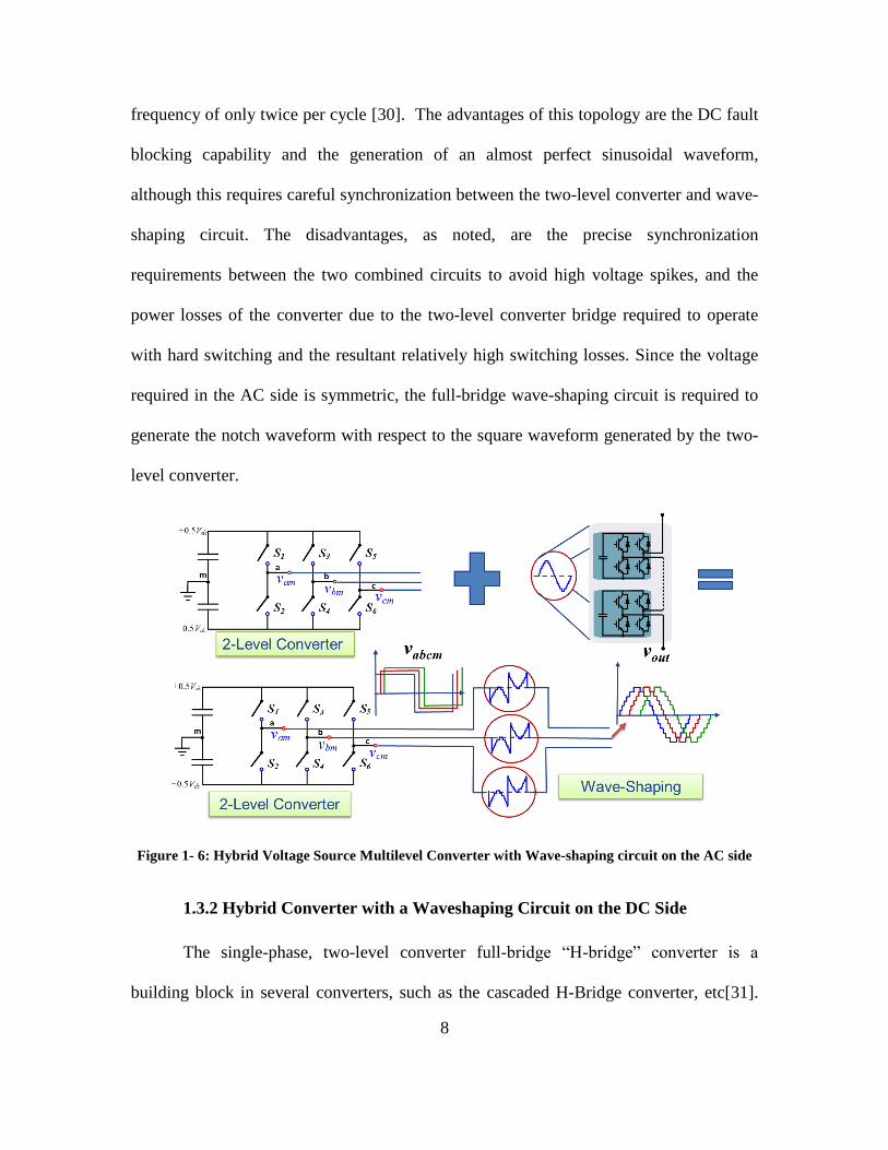
8
frequency of only twice per cycle [30]. The advantages of this topology are the DC fault
blocking capability and the generation of an almost perfect sinusoidal waveform,
although this requires careful synchronization between the two-level converter and wave-
shaping circuit. The disadvantages, as noted, are the precise synchronization
requirements between the two combined circuits to avoid high voltage spikes, and the
power losses of the converter due to the two-level converter bridge required to operate
with hard switching and the resultant relatively high switching losses. Since the voltage
required in the AC side is symmetric, the full-bridge wave-shaping circuit is required to
generate the notch waveform with respect to the square waveform generated by the two-
level converter.
Figure 1- 6: Hybrid Voltage Source Multilevel Converter with Wave-shaping circuit on the AC side
1.3.2 Hybrid Converter with a Waveshaping Circuit on the DC Side
The single-phase, two-level converter full-bridge “H-bridge” converter is a
building block in several converters, such as the cascaded H-Bridge converter, etc[31].
9
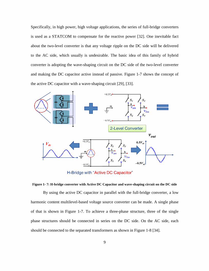
Specifically, in high power, high voltage applications, the series of full-bridge converters
is used as a STATCOM to compensate for the reactive power [32]. One inevitable fact
about the two-level converter is that any voltage ripple on the DC side will be delivered
to the AC side, which usually is undesirable. The basic idea of this family of hybrid
converter is adopting the wave-shaping circuit on the DC side of the two-level converter
and making the DC capacitor active instead of passive. Figure 1-7 shows the concept of
the active DC capacitor with a wave-shaping circuit [29], [33].
Figure 1- 7: H-bridge converter with Active DC Capacitor and wave-shaping circuit on the DC side
By using the active DC capacitor in parallel with the full-bridge converter, a low
harmonic content multilevel-based voltage source converter can be made. A single phase
of that is shown in Figure 1-7. To achieve a three-phase structure, three of the single
phase structures should be connected in series on the DC side. On the AC side, each
should be connected to the separated transformers as shown in Figure 1-8 [34].

10
Figure 1- 8: Hybrid Converter with Wave-Shaping circuit in parallel with H-Bridges
There are some advantages to this structure discussed in the literature [35]. First,
since the positive voltage is required to be generated on the DC side, the half-bridge
power cells are sufficient for use on the wave-shaping circuit. Also in this structure, three
wave-shaping circuits are required and these are located outside of the main current path.
As a result, the semiconductor power losses are expected to be lower. The fault ride-
through capability is another main advantage of this converter, since during the fault the
DC side voltage can be controlled to zero [34]. The main drawback of this converter is
the existence of the transformer which increases the size and weight of the converter.
Furthermore, there are two times as many switches on the converter,and since the two-
level converter switches operate at higher losses, this is not desirable.

11
1.3.3 Alternate-Arm Converter (AAC), Hybrid Converter with Wave-
Shaping Circuit on DC side
In the Alternate-Arm Converter structure, the wave-shaping circuits are placed on
the DC side of the main two-level converter [36]. In the AAC, the complete converter
consists of a standard two-level converter with each arm including both high voltage
switches (series of IGBTs) and a wave-shaping circuit in series. Since the wave-shaping
circuit should generate negative voltages, full-bridge sub modules are used in this
converter. Figure 1-9 shows the formation concept of the AAC.
Figure 1- 9: Alternate-Arm Converter: series of director switches with wave-shaping circuit on the
DC side

12
1.3.4 VSC-HVDC Using Multilevel Technology Review
The three manufacturers of VSC HVDC (i.e. ABB, Siemens and Alstom Grid)
have recently produced their own solutions for the modular based multilevel converters
towards the AC and DC grid side. Figure 1-10 shows the modular multilevel converter
with different sub-modules used by each of aforementioned manufacturers. After the
introduction of the MMC by Lesnicar and Marquardt [24], the first demonstration of the
converter in the HVDC application was performed by Siemens in 2007. Since then, the
converter has gained popularity due to its advantages over conventional topologies. The
multilevel topology as commercialized by Siemens is called ‘HVDC PLUS’ [37]. ABB
proposed its own MMC technology, called ‘HVDC Light,’ using press-pack IGBTs in the
valves as in the traditional two-level converter[38]. Also, Alstom developed a multilevel
topology, which adopts the hybrid concept for VSC and takes advantage of having the
capability to block the DC fault. The MMC converter commercialized by Alstom is
called ‘MaxSine’ [23]. Figure 1-11 demonstrates the commercialized VSC-HVDC
modular based multilevel converters from Siemens, ABB and Alstom Grid.
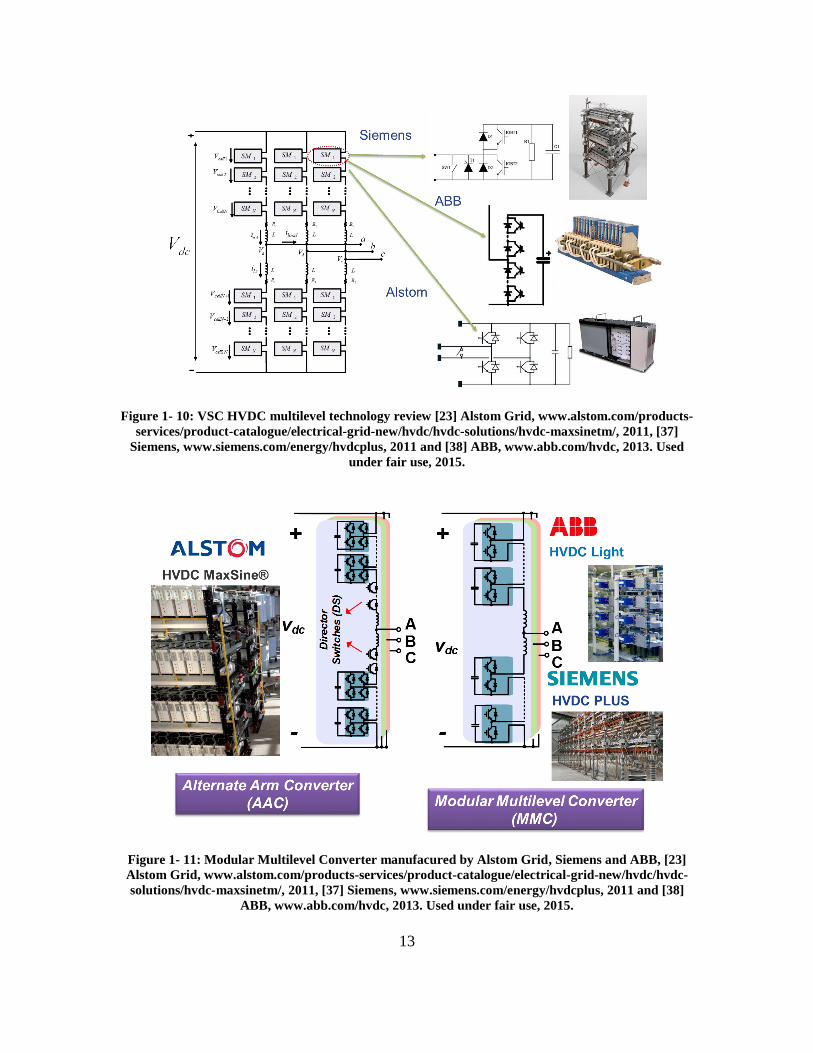
13
Figure 1- 10: VSC HVDC multilevel technology review [23] Alstom Grid, www.alstom.com/products-
services/product-catalogue/electrical-grid-new/hvdc/hvdc-solutions/hvdc-maxsinetm/, 2011, [37]
Siemens, www.siemens.com/energy/hvdcplus, 2011 and [38] ABB, www.abb.com/hvdc, 2013. Used
under fair use, 2015.
Figure 1- 11: Modular Multilevel Converter manufacured by Alstom Grid, Siemens and ABB, [23]
Alstom Grid, www.alstom.com/products-services/product-catalogue/electrical-grid-new/hvdc/hvdc-
solutions/hvdc-maxsinetm/, 2011, [37] Siemens, www.siemens.com/energy/hvdcplus, 2011 and [38]
ABB, www.abb.com/hvdc, 2013. Used under fair use, 2015.
14
1.4 Research Objectives
Due to the continuous emergence of Modular Multilevel Converters, many
questions about their modeling, control, advantages and disadvantages arise.
Consequently, a significant effort has been devoted to developing the converter for
medium voltage applications such as motor drives. Since the design of the MMC requires
a good understanding of the operation principles of the converter, first the modeling
approach should be chosen to provide an analysis of the converter’s operation. Another
issue to consider will be the design of the MMC controller for the MMC, which can be
accomplished by modeling the MMC in DQ reference frame. Next, a detailed control
approach to the MMC should be discussed, and the circulating current suppressing
controller design and capacitor voltage balance should be considered as one of the
important points of the MMC’s operation. Some of the main drawbacks of the MMC will
be addressed in this study. One of these drawbacks is with regard to the capacitor bank
design of the MMC and maximizing the reliability of the converter. A reliability-oriented
design of the capacitor bank is therefore considered to be important in the practical setup
of the MMC. The design of the capacitor bank and arm inductor will influence the
operation of the MMC and therefore explained herein. The switching frequency design of
the MMC also needs to be addressed. In high and medium voltage applications, to
prevent high semiconductor switching losses, the switching frequency tends to be set as
low. However, the operation of the converter in low switching frequencies, means higher
voltage ripple stress on the capacitor and IGBT in each cell. Therefore, an even trade-off
between switching losses and capacitor voltage ripple should be achieved. This even
trade-off can be obtained by using the reliabiltiy function of the converter as the objective

15
function. The reliability of the converter should be extracted by considering the reliability
models of the individul components in the MMC. System-level reliabiltiy modeling for
power electronics converters, especially high power converters such the MMC, is not
discussed in the literature since one of the advantages of the MMC is it’s high reliability
as a result of its modular structure. The Markov model is one of the mathematical
appraoches that is used in many application and is one a great candidate to model the
reliablity of the MMC, as it models the fault transients of the converter. Therefore, in this
thesis, the switching frequency design of the modular multilevel converters is peresented
using the Markov state-space reliability model of the converter as the objective function
that needs to be maximized.
But the main issue regarding the MMC with half-bridge power modules is their
lack of DC fault blocking capabiltiy, which is a result of their half-bridge structure. In an
MMC with half bridge power cells, there exists an uncontrolled current path during the
DC short circuit fault and the only way to remove the fault is using DC or AC circuit
breakers, which add more complexity and cost to the converter. One promising way to
provide DC fault ride capacibiltiy for the MMC is to use an MMC with full-bridge power
cells or the newly conceived hybrid mulitilevel converters, among which is the recently
commercialized Alternate Arm Converter. The operation of the AAC modeling and
control are not completely addressed in the litrature and there is wide research headroom
availbe for the AAC. The existance of the series IGBT “director switches” in series with
the arm inductor and stacked full-bridge in the AAC, means that it requires zero current
switching of the devices, which in turn prevents the converter from huge voltage spikes
as a result of the fast di/dt. Therefore, the ZCS operation of the director switches for the

16
AAC should be studied. The next step will be DC fault analysis of the modular multilevel
converters with regard to the their interest topologies: MMC with half-bridge, MMC with
full-bridge power cells, and the AAC. The DC fault control of the MMC is not discussed
in the literature either. So, the following are proposed in this thesis: DC fault control of
the MMC with full-bridge and an AAC for use in limiting DC fault as well as in
maintaining the capacitor voltage during the DC. This research targets the following
goals:
1- Modeling of the modular multilevel converters (MMC and AAC).
2- Closed-loop control of the circuling current, capacitor voltage and energy balance
and closed loop output load current loop as well as DC fault control for the
modular multilevel converters (MMC and AAC).
3- High Reliability Capacitor Bank Design of the modular multilevel converters.
4- Reliability Oriented Switching Frequency Analysis of the modular multilevel
converters.
5- Operation principles and Zero Current Switching of the director switches in the
AAC.
6- DC- Fault ride-through capabiltiy of the modular multilevel converters (MMC
and AAC).
1.5 Thesis Organization
To satisfy the above objectives, this thesis is organized as follows. Chapter 2
introduces the modular multilevel converters’ modeling, and provides modeling of the
complete switching, average, and DQ reference frame modeling of the MMC, and also
17
the switching and average modeling of the AAC. Chapter 3 explores the closed loop
control of the modular multilevel converters. Particular attention is paid to the Circulating
Current Suppressing Control (CCSC) and capacitor voltage balance in the MMC and the
overlap time control for the AAC. Chapter 4 evaluates the novel consideration regarding
to design of the Modular Multilevel Converters including MMC and AAC. The Zero
Current Switching scheme for the director switches in the AAC is proposed in this
chapter as well as reliabitliy oriented design of the modular multilevle converters.
Chapter 5 presents a DC fault ride through capabiltiy of the modular multilevel
converters. Conclusions will then be drawn in Chapter 6, followed by a discussion of the
future work.
18
Chapter 2 Modular Multilevel Converters Modeling
2.1 Introduction
This chapter presents the modeling approach for illustrating the operation
principles of Modular Multilevel Converters (MMC) including the MMC with half-
bridge power cells and the Alternate-Arm Converter (AAC). Modular multilevel
converters have emerged as new multilevel converters that can be used especially in High
Voltage Direct Current (HVDC) and Medium Voltage Direct Current (MVDC)
applications [25],[39-42]. Generally, the main advantages of the MMC with as compared
to other types of multilevel converters are their high modularity and cabability for high
voltage scalability, which means that they can be connected directly to the grid without
using any transformer [43]. The modular multilevel converter structure is shown in
Figure 2-1. The MMC generally consists of upper and lower arm power cells, which can
be half-bridge or full-bridge. The first model of the MMC was generated by replacing the
single switches in a two-level converter with a series of power modules. As mentioned,
these power modules can be half-bridge or full-bridge; however, due to the higher
number of switches and switching power losses, MMC with half-bridge is more oftren
developed. In order to eliminate inrush current during switching between modules,
additional inductors should be added in series with the power modules in each arm
19
[44].To have sinusoidal output voltage, the upper arm and lower modules’ references
should be justified with respect to the DC voltage in order to generate a proper wave-
shaping circuit [29]. In the MMC with the half-bridge, the maximum voltage over each
module is the DC-link voltage divided by the number of arm modules; however, the
MMC with the full-bridge module can work in over-modulation since each module can
generate negative voltage as well [45].
a
b
c
2
dcp
VE
2
dcn
VE
1cellV
2cellV
CellNV
1cellNV
2cellNV
NcellV 2
uAi
lAi
aVbV
cV
loadi
LR
LL
LR
LL
LR
LL
Figure 2- 1: Modular Multilevel Converter topology with each sub-module structure.
One of the disadvantages of the MMC is the existence of relatively high
circulating current due to the difference in voltage of the arm inductors [46]-[47]. To
limit the circulating current, the arm inductor size should be selected to be quite high or
the circulating current suppressing controller should be employed [48]. Another issue
regarding this topology is the number of capacitor banks required for each module in the
MMC, which can lead to a huge space occupied by capacitors and cause reliability issues

20
[49]-[50]. ] Moreover, having a high number of modules makes the control system more
complex [51]. Significant efforts have been dedicated to the modeling of the MMC and to
a circuit behavior analysis of the converter. Different modeling approaches for the
Modular Multilevel Converter (MMC) have been carried out in the literature. In [52], the
state-space switching model of the MMC is developed and the complete derivation
procedure of that is given. In reference [53], a continuous model of a three phase MMC,
which is derived from ordinary differential equations, is developed and described. All the
other existent models deal with the three-phase average model of the MMC, and the
equations are extracted based on the average model [52-57].
In this chapter, a new modeling approach based on D-Q frame modeling is
proposed for use as a model-based converter of the inner and outer loop control design.
DQ modeling of the MMC can provide the relations of the duty cycles and arm quantities
as well as the output voltage and current of the converter. Also, the proposed DQ model
of the MMC is of great value in developing new control methods for the MMC. To obtain
the DQ model, the following procedure should be taken. First of all, a three-phase
average model of the converter should be derived from the switching model. Then by
applying the Park transformation, the DQ model can be achieved. The second order
harmonic circulating current is considered as the dominant component of the circulating
current and higher order harmonics are considered to be negligible [47]. Therefore, the
MMC system can be divided into three-frames of operation: DC, fundamental frequency,
and twice the fundamental frequency frame. By assuming the superposition, each of the
parameters can be modeled in these three-frames and finally the results can be added
together. Indeed, using this model, DC current and circulating current equations can be

21
decoupled from the load current. By changing the modeling of MMC into three separate
models, one will be able to derive the DQ model in each case.
2.2 Modular Multilevel Converter Modeling (MMC)
2.2.1 MMC Switching Model
The general state-space switching model is derived based on the simplest MMC
configuration: a single-module MMC topology as shown in Figure 2-1 [52]. The state-
space model is derived by selecting the inductor currents and capacitor voltages as states
of the converter for control purposes. Therefore, five totally independent KVL equations
can be written for the converter and iUabc (Upper Arm Current phase a, b and c), iLabc
(Lower Arm Current phase a, b and c) can be chosen as initial independent state
variables. However, the DC current, line currents and circulating currents are the most
convenient parameters to describe and control the operation of the converter, and the
fundamental circuit characteristics of the MMC can be better reflected based on them.
Hence, the initial state variables should be changed into another set of independent states
in terms of the three latter current components. Figure 2-2 shows the switching model of
the MMC.

22
SUa1
POS
Neg
am
SUa2
SLa1
SLa2
vCUa
vCLa
iUa
ia
iLa
SUb1
SUb2
SLb1
SLb2
vCUb
vCLb
iUb
iLb
idc SUc1
SUc2
SLc1
SLc2
vCUc
vCLc
iUc
iLc
b c
n
vSa
ib ic
+0.5Vdc
‒0.5Vdc
L
L
L
L
L
L
C
C
C
C
C
CSLa∙vCLa SLb∙vCLb SLc∙vCLc
SUa∙vCUa SUb∙vCUb SUc∙vCUc
vSb vSc
Figure 2- 2: Switching Model of the MMC.
The SUx and SLx are defiend as the switching functions that can be ‘1’ or ‘0’,
where x is a phase identifier, given by (2-1).
itchedLowerArmSw
itchedUpperArmSwSUx
0
1 (2-1)
By using an intermediate state variable transformation as in (2-2) and (2-3), the
new state variables can be obtained as the sum of phase-leg currents, named “sum
current,” and the subtraction of the upper and lower arm current, which gives the line
currents. These currents are very important intermediate state variables that will help
derive DC current and line current equations.
LxUxsumx iii (2-2)
LxUxx iii (2-3)
under the assumption (2-4), the DC current equation can be derived using KCL as
shown in (2-5),
cbax
sumx
cbax
xsumx
cbax
Uxdc iiiii,,,,,, 2
1
2
1 (2-4)
0 cba iii (2-5)
23
The AC line current equations can be expressed as shown in (2-6), where vnm is
the common-mode voltage between the AC neutral and the DC mid-point is given by (2-
7):
L
vvvSvSi
dt
d sxnmUxUxLxLxx
22 (2-6)
cbax
UxUxLxLxnm vSvSv,,6
1 (2-7)
Through the intrinsic operation of the MMC, there exsits the circulating current
which circulates between phase-legs without flowing into the DC bus or the AC lines.
Their equation is derived by the KVL equation through the circulating current path as
shown below.
cbax
UxUxUxUxLxLxUxUxcirx vSvSvSvSL
idt
d
,,
36
1 (2-8)
Lastly, the full-rank current equations for the state-space model of the MMC are
given in (2-9).
LbLbUbUb
cbax
LxLxUxUxcirb
LaLaUaUa
cbax
LxLxUxUxcira
sbnmUbUbLbLbb
sanmUaUaLaLaa
cbax
LxLxUxUxdcdc
vSvSvSvSL
idt
d
vSvSvSvSL
idt
d
L
vvvSvSi
dt
d
L
vvvSvSi
dt
d
vSvSVL
idt
d
36
1
36
1
22
22
32
1
,,
,,
,,
(2-9)
24
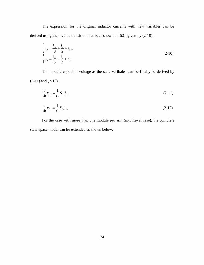
The expression for the original inductor currents with new variables can be
derived using the inverse transition matrix as shown in [52], given by (2-10).
cirxxdc
Lx
cirxxdc
Ux
iii
i
iii
i
23
23 (2-10)
The module capacitor voltage as the state varibales can be finally be derived by
(2-11) and (2-12).
UxUxUx iSC
vdt
d 1 (2-11)
LxLxLx iSC
vdt
d 1 (2-12)
For the case with more than one module per arm (multilevel case), the complete
state-space model can be extended as shown below.
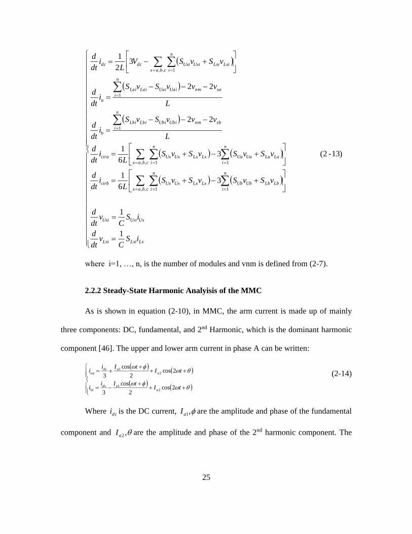
25
LxLxiLxi
UxUxiUxi
n
i
LbLbUbUb
cbax
n
i
LxLxUxUxcirb
n
i
LaLaUaUa
cbax
n
i
LxLxUxUxcira
sbnm
n
i
UbiUbiLbiLbi
b
sanm
n
i
UaiUaiLaiLai
a
cbax
n
i
LxiLxiUxiUxidcdc
iSC
vdt
d
iSC
vdt
d
vSvSvSvSL
idt
d
vSvSvSvSL
idt
d
L
vvvSvS
idt
d
L
vvvSvS
idt
d
vSvSVL
idt
d
1
1
36
1
)13-2(36
1
22
22
32
1
1,, 1
1,, 1
1
1
,, 1
where i=1, …, n, is the number of modules and vnm is defined from (2-7).
2.2.2 Steady-State Harmonic Analyisis of the MMC
As is shown in equation (2-10), in MMC, the arm current is made up of mainly
three components: DC, fundamental, and 2nd Harmonic, which is the dominant harmonic
component [46]. The upper and lower arm current in phase A can be written:
tItIi
i
tItIi
i
aadc
la
aadc
ua
2cos2
cos
3
2cos2
cos
3
21
21
(2-14)
Where dci is the DC current, ,1aI are the amplitude and phase of the fundamental
component and ,2aI are the amplitude and phase of the 2nd harmonic component. The

26
average switching functions of the upper and lower arm of the MMC in general form are
given by:
)cos(2
1
)cos(2
1
tDd
tDd
lla
uua (2-15)
The average capacitor current for the upper arm will be given by:
uauacua idi (2-16)
By replacing (2-14) and (2-15) in (2-16), the average capacitor current is obtained
as:
2
)3cos(
2
)2cos(
4
)2cos(
2
)cos(
4
)cos(
3
)cos(
4
)cos(
6
22
1211
tIDtI
tIDtIDtItiDIDii
aua
auauadcuaudccua (2-17)
From the capacitor current, the capacitor voltage can be obtained by using the
following relation:
dtiC
v cuacua
1 (2-18)
By replacing (2-17) in (2-18) and taking the integral we have:
C
tID
C
tI
C
tID
C
tID
C
tI
C
tiDt
IDi
CVv
auaau
auadcuaudcdccua
6
)3sin(
4
)2sin(
8
)2sin(
2
)sin(
4
)sin(
3
)sin(
4
)cos(
6
1
221
211
(2-19)
Where, dcV is the DC-link voltage. From the capacitor voltage, the module voltage
can be obtained:
cuauaua vdv (2-20)
By replacing (2-19) into (2-20):

27
...12
)2sin(
4
)2sin(
8
)2sin(
6
)22sin(
8
)2sin(
16
)2sin(
8
)sin(
16
)sin()cos(
4
)sin(
8
)sin(
6
)sin()cos(
24
)2sin(
8
)sin(
2
2
2
2
2
1
2
21
21
2
21
2
2
1
termsorderhigherC
tID
C
tID
C
tID
C
tiD
C
tI
C
tID
C
tID
C
tIDtVD
C
tID
C
tI
C
tiDttvD
tv
C
ID
C
IDVv
au
auaudcuaau
auaudcu
aua
dcucudcu
cudcauaudcua
(2-21)
And similarly for the lower arm we get:
...
12
)2sin(
4
)2sin(
8
)2sin(
6
)22sin(
8
)2sin(
16
)2sin(
8
)sin(
16
)sin()cos(
4
)sin(
8
)sin(
6
)sin()cos(
24
)2sin(
8
)sin(
2
2
2
2
2
1
2
2
121
2
2
12
2
1
termsorderhigher
C
tID
C
tID
C
tID
C
tiD
C
tI
C
tID
C
tID
C
tIDtVD
C
tID
C
tI
C
tiDttvD
tv
C
ID
C
IDVv
alalaldcla
alalaldcl
al
adclcldcl
cldcalaldcla
(2-22)
At the steady state, we have DDD lu and 0 cldccudc vv .
2.2.3 Average Model of the MMC
The MMC switching model with only one cell in each arm is shown in Figure 2-3
(a).
A
m
+0.5Vdc
-0.5Vdc
+
VCu
-
LL
RL
L
iua
ila
ia
LLL
RL
LL
RL
ib
ic
B
C
+
VCl
-
nR
R
+
vu
-
+
vl
-
(a)
A
+
VCua
-
L
ia
L ib
+
VCla
-
R
R
+
vua
-
+
vla
-
B
L
L
R
R
C
L
L
R
R
+
vub
-
+
vuc
-
+
vlb
-
+
vlc
-
idc/3+ici ra
iua
ila
iub
ilb
iuc
ilc
idc/3+ici rb idc/3+ici rc
(b)
Figure 2- 3 (a) Switching model of MMC with one power cell in each arm, (b) Circulating current
switching model in the MMC

28
From the MMC switching model, by applying KVL in the upper and lower arm,
we get the following switching model equations:
01
)(12
:)(
01
)(12
:)(
nmabcL
abc
Llabc
labc
abccll
dc
nmabcL
abc
Luabc
uabc
abccuu
dc
viR
dt
idLiR
dt
idLvS
VLower
viR
dt
idLiR
dt
idLvS
VUpper
(2-23)
Where ucuu vvS , lcll vvS , uS and lS are the switching functions of the upper
and lower arm, cuv and clv are the capacitor voltages of the upper and lower arm
capacitors, L and R are the inductance and the resistance of the modules, LR and LL are
the load resistance and inductor, abci are the line currents in the phases a, b and c, and nmv
is the voltage from the load neutral to the DC side neutral point
cbax cuxuxclxlxnm vSvSv,,6
1 , and 1 is the column vector given by T1111 . Adding the
above two equations we get:
01222
)()(
nmabc
LabcL
labcuabclabcuabc
abccllabccuu
vdt
idLiR
iiRdt
iidLvSvS
(2-24)
By replacing abclabcuabc iii , equation (2-24) will be changed to:
01222
)()(
nmabc
LabcL
abcabc
abccllabccuu
vdt
idLiR
iRdt
idLvSvS
(2-25)
The equations for the module capacitors are given by:

29
abccllclabc
abccuucuabc
iSCdt
vd
iSCdt
vd
1
1
(2-26)
Where cuabcv , clabcv are the capacitor voltages of the upper and lower arm in phases
a, b and c, C is the capacitance of the module, ui and li are the upper and lower arm
currents. As is mentioned for the MMC, because of the existence of the arm inductors,
there exists a circulating current which doesn’t come into the DC side but just circulates
through each phase. To account for the circulating current, as can be seen in Figure 2-3
(b), we have the following equations:
0)()(
)(
)()(
ualauala
cuauaclala
lbublbub
clblbcubub
iiRdt
iidLvSvS
iiRdt
iidLvSvS
(2-27)
Similarly, for the other two phases we get:
0)()(
)(
)()(
0)()(
)(
)()(
uclcuclc
cucuaclclc
lcuclaua
clalacuaua
ublbublb
cububclblb
lcuclcuc
clclccucuc
iiRdt
iidLvSvS
iiRdt
iidLvSvS
iiRdt
iidLvSvS
iiRdt
iidLvSvS
(2-28)
Since, ciradclaua iiii 23
2 substituting in (2-28) we get:
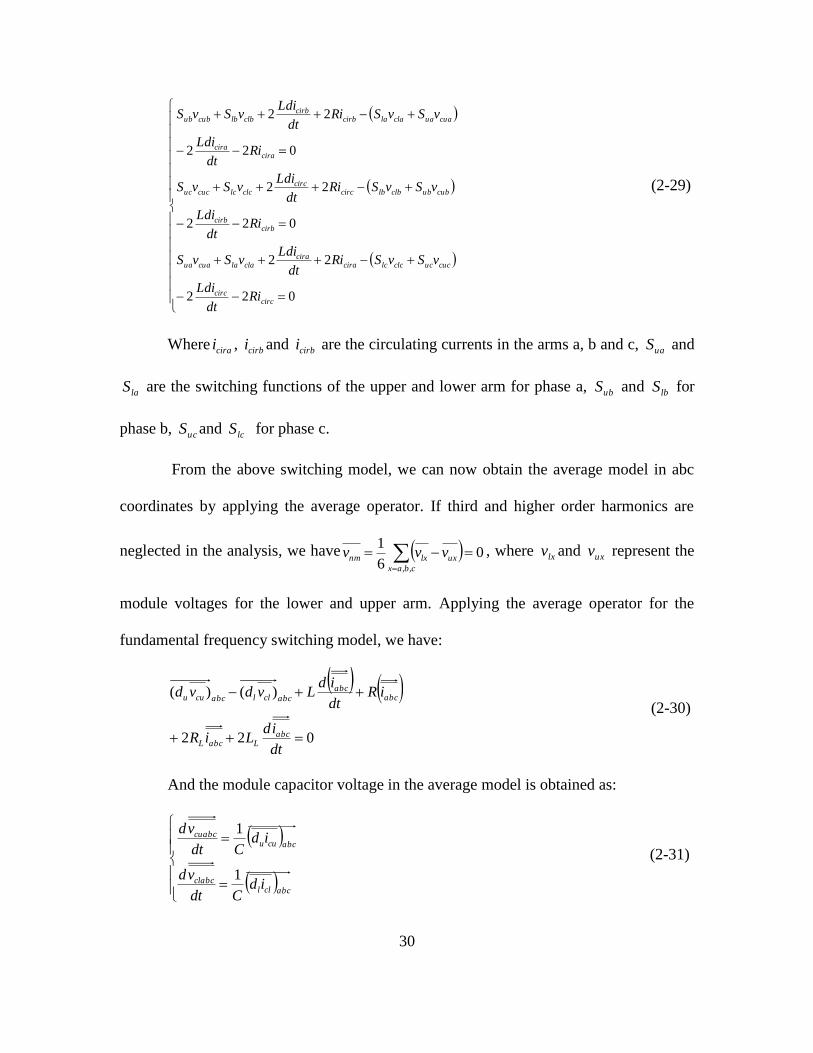
30
022
22
022
22
022
22
circcirc
cucucclclcciracira
clalacuaua
cirbcirb
cububclblbcirccirc
clclccucuc
ciracira
cuauaclalacirbcirb
clblbcubub
Ridt
Ldi
vSvSRidt
LdivSvS
Ridt
Ldi
vSvSRidt
LdivSvS
Ridt
Ldi
vSvSRidt
LdivSvS
(2-29)
Where cirai , cirbi and cirbi are the circulating currents in the arms a, b and c, uaS and
laS are the switching functions of the upper and lower arm for phase a, ubS and lbS for
phase b, ucS and lcS for phase c.
From the above switching model, we can now obtain the average model in abc
coordinates by applying the average operator. If third and higher order harmonics are
neglected in the analysis, we have 06
1
,,
cbax
uxlxnm vvv , where lxv and uxv represent the
module voltages for the lower and upper arm. Applying the average operator for the
fundamental frequency switching model, we have:
022
)()(
dt
idLiR
iRdt
idLvdvd
abcLabcL
abcabc
abccllabccuu
(2-30)
And the module capacitor voltage in the average model is obtained as:
abccllclabc
abccuucuabc
idCdt
vd
idCdt
vd
1
1
(2-31)
31
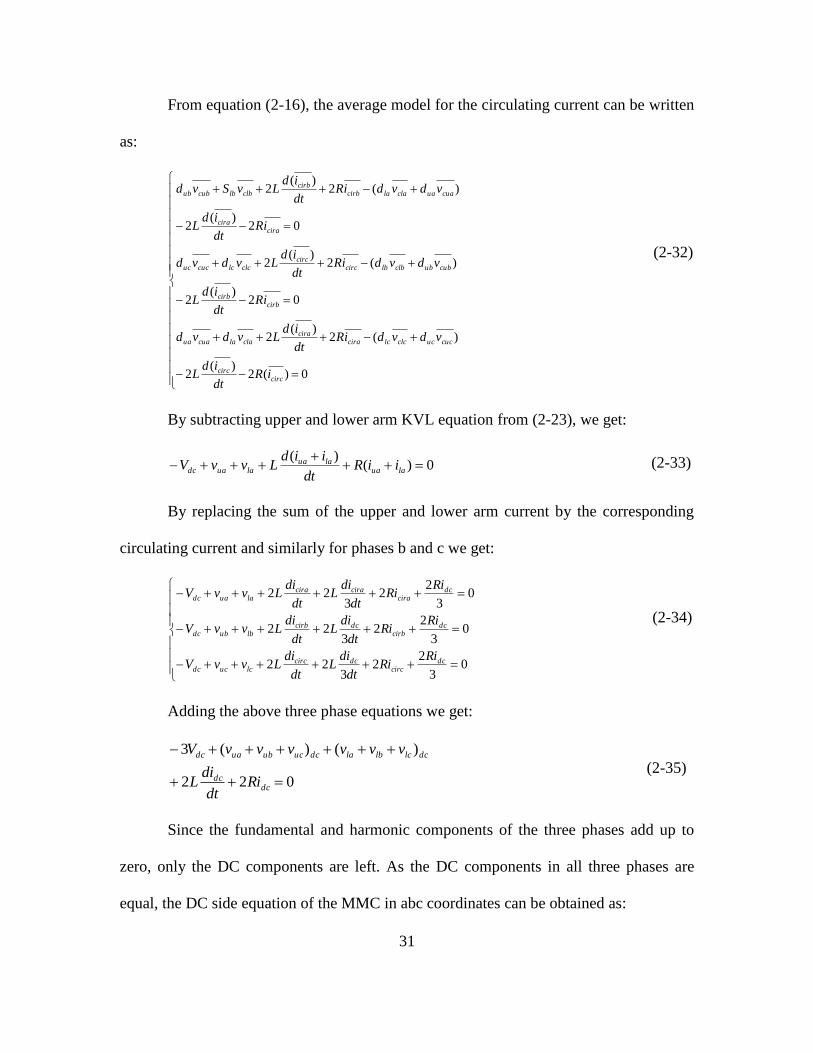
From equation (2-16), the average model for the circulating current can be written
as:
0)(2)(
2
)(2)(
2
02)(
2
)(2)(
2
02)(
2
)(2)(
2
circcirc
cucucclclcciracira
clalacuaua
cirbcirb
cububclblbcirccirc
clclccucuc
ciracira
cuauaclalacirbcirb
clblbcubub
iRdt
idL
vdvdiRdt
idLvdvd
iRdt
idL
vdvdiRdt
idLvdvd
iRdt
idL
vdvdiRdt
idLvSvd
(2-32)
By subtracting upper and lower arm KVL equation from (2-23), we get:
0)()(
laualaua
lauadc iiRdt
iidLvvV (2-33)
By replacing the sum of the upper and lower arm current by the corresponding
circulating current and similarly for phases b and c we get:
03
22
322
03
22
322
03
22
322
dccirc
dccirclcucdc
dccirb
dccirblbubdc
dccira
ciraciralauadc
RiRi
dt
diL
dt
diLvvV
RiRi
dt
diL
dt
diLvvV
RiRi
dt
diL
dt
diLvvV
(2-34)
Adding the above three phase equations we get:
022
)()(3
dcdc
dclclbladcucubuadc
Ridt
diL
vvvvvvV
(2-35)
Since the fundamental and harmonic components of the three phases add up to
zero, only the DC components are left. As the DC components in all three phases are
equal, the DC side equation of the MMC in abc coordinates can be obtained as:
32
0)(2
3 dc
dcdcucubuadc Ri
dt
diLvvvV (2-36)
Where dcV is the DC voltage and uav , ubv and ucv represent the module voltages in
the phases a, b and c. From (2-30), (2-31) for phase current model, (2-32) for the
circulating current model and (2-10) for the DC current model in three-phase abc
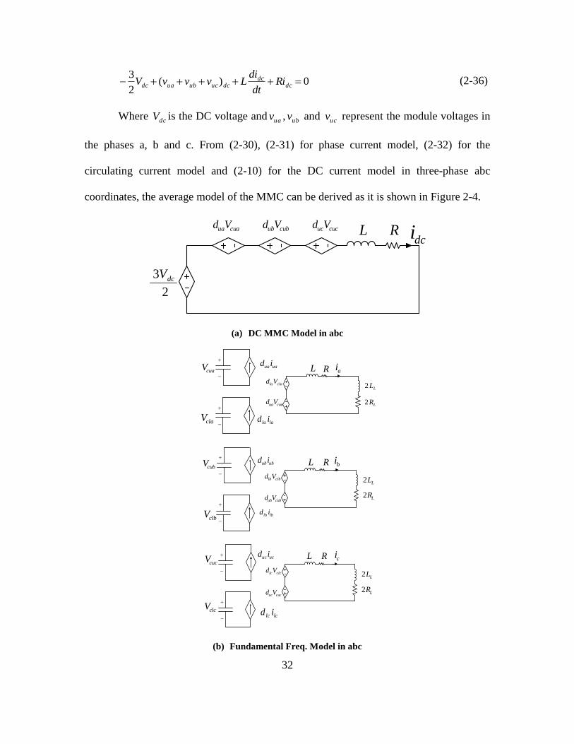
coordinates, the average model of the MMC can be derived as it is shown in Figure 2-4.
2
3 dcV
L RdcicuauaVd cububVd cucucVd
(a) DC MMC Model in abc
L R
LR2
clalaVd
cuauaVd
aiuauaid
lala id
cuaV
claV
LL2
L R biububid
lblb id
cubV
clbV
LR2
LL2clblbVd
cububVd
ciucuc id
lclc id
cucV
clcV
LR2
LL2clclcVd
cucucVd
L R
(b) Fundamental Freq. Model in abc

33
cuauaVd
clalaVd
L
R
L
R
L
R
L
R
cububVd
clblbVd clclcVd
cucucVd
LR
L
R
ciraicirbi circi
(c) Circulating Current Model in abc
Figure 2- 4 abc Average Model for the MMC.
2.2.4 D-Q Model of the MMC
By obtaining the DC current, phase current, and circulating current in the three-
phase abc model, the DQ model from them can be extracted.
2.2.4.1 D-Q Model of Phase Current in the MMC
From the average model of MMC (2-30), the fundamental frequency model
frame, we have:
022
abcLabc
Labc
abc
labcuabc iRdt
idLiR
dt
id
Lvv (2-37)
For the phase a, by substituting the fundamental frequency components of uav and
lav from (2-21) and (2-22) in (2-37), we get:
0224
)sin(
8
)sin()cos(2
2
)sin(
4
)sin(
3
)sin()cos(2
2
1
2
2
1
dt
diLiRRi
dt
Ldi
C
tDI
C
tIDtDV
C
tDI
C
tI
C
tDittDv
aLaLa
a
dc
dccudc
(2-38)
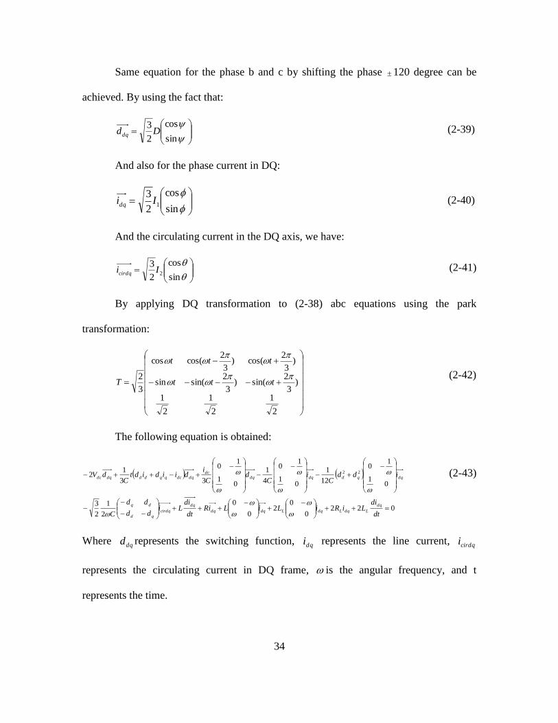
34
Same equation for the phase b and c by shifting the phase 120 degree can be
achieved. By using the fact that:
sin
cos
2
3Dddq
(2-39)
And also for the phase current in DQ:
sin
cos
2
31Iidq
(2-40)
And the circulating current in the DQ axis, we have:
sin
cos
2
32Iicirdq
(2-41)
By applying DQ transformation to (2-38) abc equations using the park
transformation:
2
1
2
1
2
1
)3
2sin()
3
2sin(sin
)3
2cos()
3
2cos(cos
3
2
ttt
ttt
T (2-42)
The following equation is obtained:
0220
02
0
0
2
1
2
3
01
10
12
1
01
10
4
1
01
10
33
12 22
dt
diLiRiLiLiR
dt
diLi
dd
dd
C
iddC
iC
dC
idiididt
CdV
dq
LdqLdqLdqdq
dq
cirdq
qd
dq
dqqddqdqdc
dqdcqqdddqdc
(2-43)
Where dqd represents the switching function, dqi represents the line current, cirdqi
represents the circulating current in DQ frame, is the angular frequency, and t
represents the time.

35
2.2.4.2 DQ Model of DC and Circulating Current in the MMC
From the average model of circulating current in abc coordinates (2-32) we get:
023
2)(22)(
023
2)(22)(
023
2)(22)(
circ
circ
lcuccira
cira
laua
cirb
cirb
lbubcirc
circ
lcuc
cira
cira
lauacirb
cirb
lbub
iRdt
idLvviR
dt
diLvv
iRdt
idLvviR
dt
diLvv
iRdt
idLvviR
dt
diLvv
(2-44)
Substituting the double line frequency values of lclblaucubua vvvvvv ,,,,, from (2-19)
and (2-21) in (2-44), the DQ model of the circulating current can be achieved by:
022
6
)2sin(
3
)22sin(
4
)2sin()21(
8
)2sin(32
2
6
)3
22sin(
3
)3
222sin(
4
)3
22sin(
)21(8
)3
22sin(
3
2
22
2212
2
2
22
1
ciraciradc
cirbcirb
dc
Ridt
Ldi
C
tID
C
tiD
C
tID
C
tDIRi
dt
Ldi
C
tID
C
tiD
C
tI
DC
tDI
(2-45)
Similarly, for the other two phases, the same equation can be achieved by
phase shifting of (2-45) 120 degree. Applying the park transformation for the negative
sequence 2nd harmonic components as it is given by:
2
1
2
1
2
1
)3
22sin()
3
22sin(2sin
)3
22cos()
3
22cos(2cos
3
2
ttt
ttt
T
(2-46)
And using the fact that:
cirqcird
cirqcird
cirdq
ii
iii
2
3
2
12
3
2
1
' (2-47)
Where cirabccirdq iTi 2 and cirbcacirdq iTi 2
' , we get:

36
020
6316
6
01
10
92
0
02
01
10
8
122
dq
qd
ddcdq
qd
dq
cirdq
qd
cirdqcirdqcirdq
cirdq
ddd
d
C
ii
dd
dd
C
iC
ddiLi
CiR
dt
iLd
(2-48)
Plus, the DC side equation can also be expressed in d-q coordinates as:
0
4442
3
2
3
2 22
qqdddc
qddqcirqqdcirdqd
dcdc ididi
C
t
C
id
C
id
C
idd
C
idd
Ridt
Ldi
(2-49)
From (2-43), (2-48) and (2-49) the DQ model of the MMC for the phase current,
DC current, and circulating current is obtained. The DQ model of the MMC from these
equation can be drawn as shown in Figure 2-5.
c
t
4
cirqi
C23
2
L
R
dci
C
id dq
4
cird
qdi
C
dd
3
2
C
id qd
4
dd2
qd2
dci dd di qiqd
(a) DC Model in D-Q
c
t
3
C
id dcq
3
LL2
R
di
ddcdV2
C
id cirdq
2
2
3
C
id cirqd
2
2
3
LR2
qd
C
dd
12
12
22
L
L
LL
dciqiqddidd dd
qiC4
qdc
t
3
C
id dcd
3
qdc dV2
qd
LC
dd
CLL
124
12
22
C
id cirdd
2
2
3
C
id cirqq
2
2
3
LL2
R
LR2
L
qidci
qiqddidd
di
(b) Fundamental Freq. Model in D-Q
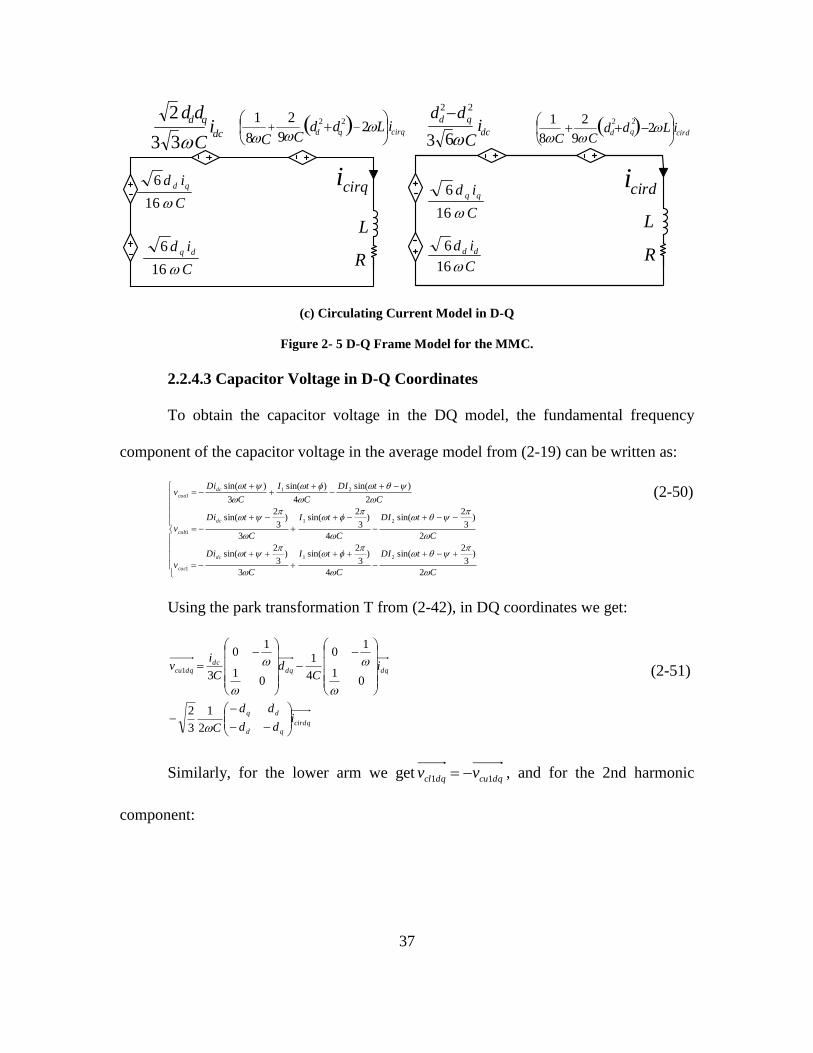
37
C
id qd
16
6
dciC33
2
L
R
cirqi
qd LddCC
2
9
2
8
1 22
C
id dq
16
6
qdddcirqi
C
id qq
16
6
dc
qdi
C
dd
63
22
L
R
cirdi
LCC
2
9
2
8
1
C
id dd
16
6
cirdi
dd2
qd2
(c) Circulating Current Model in D-Q
Figure 2- 5 D-Q Frame Model for the MMC.
2.2.4.3 Capacitor Voltage in D-Q Coordinates
To obtain the capacitor voltage in the DQ model, the fundamental frequency
component of the capacitor voltage in the average model from (2-19) can be written as:
C
tDI
C
tI
C
tDi
v
C
tDI
C
tI
C
tDi
v
C
tDI
C
tI
C
tDiv
dc
cuc
dc
cub
dc
cua
2
)3
2sin(
4
)3
2sin(
3
)3
2sin(
2
)3
2sin(
4
)3
2sin(
3
)3
2sin(
2
)sin(
4
)sin(
3
)sin(
21
1
21
1
21
1 (2-50)
Using the park transformation T from (2-42), in DQ coordinates we get:
cirdq
qd
dq
dqdqdc
dqcu
idd
dd
C
iC
dC
iv
2
1
3
2
01
10
4
1
01
10
31 (2-51)
Similarly, for the lower arm we get dqcudqcl vv 11 , and for the 2nd harmonic
component:
38
C
tI
C
tDI
v
C
tI
C
tDI
v
C
tI
C
tDIv
cuc
cub
cua
4
)3
22sin(
8
)3
22sin(
4
)3
22sin(
8
)3
22sin(
4
)2sin(
8
)2sin(
21
2
21
2
212
(2-52)
Using the transformation 2T , in DQ coordinates we get:
cirdqdq
qd
dq
dqcu iC
idd
dd
Cv
01
10
4
1
8
1
3
22
(2-53)
Similarly, for the lower arm we get:
dqcudqcl vv 22 (2-54)
From (2-38) and (2-40), the capacitor voltage in the DQ frame can be obtained.
2.2.5 Simulation Results
In this section, simulation analysis has been done to evaluate the new modeling in
the DQ frame and to compare it with the three phase abc and switching model. The
simulation specifications are given in Table 2-1. All three models (i.e. three-phase
switching and average model and DQ model) are simulated in the Simulink/ Matlab. The
switching model of the MMC is verified experimentally in the literature [42], [46] and
[47].
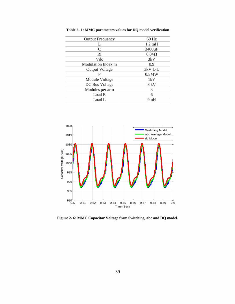
39
Table 2- 1: MMC parameters values for DQ model verification
Output Frequency 60 Hz
L 1.2 mH
C 3400µF
Ri 0.04Ω
Vdc 3kV
Modulation Index m 0.9
Output Voltage 3kV L-L
P 0.5MW
Module Voltage 1kV
DC Bus Voltage 3 kV
Modules per arm 3
Load R 6
Load L 9mH
Figure 2- 6: MMC Capacitor Voltage from Switching, abc and DQ model.
0.5 0.51 0.52 0.53 0.54 0.55 0.56 0.57 0.58 0.59 0.6980
985
990
995
1000
1005
1010
1015
1020
Time (Sec)
Capacitor
Voltage (
Volt)
Switching Model
abc Average Model
dq Model
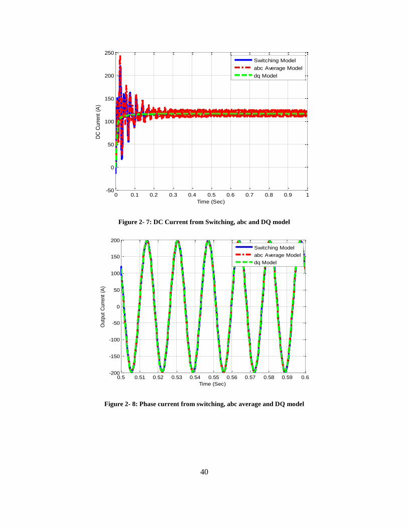
40
Figure 2- 7: DC Current from Switching, abc and DQ model
Figure 2- 8: Phase current from switching, abc average and DQ model
0 0.1 0.2 0.3 0.4 0.5 0.6 0.7 0.8 0.9 1-50
0
50
100
150
200
250
Time (Sec)
DC
Curr
ent
(A)
Switching Model
abc Average Model
dq Model
0.5 0.51 0.52 0.53 0.54 0.55 0.56 0.57 0.58 0.59 0.6-200
-150
-100
-50
0
50
100
150
200
Time (Sec)
Outp
ut
Curr
ent
(A)
Switching Model
abc Average Model
dq Model
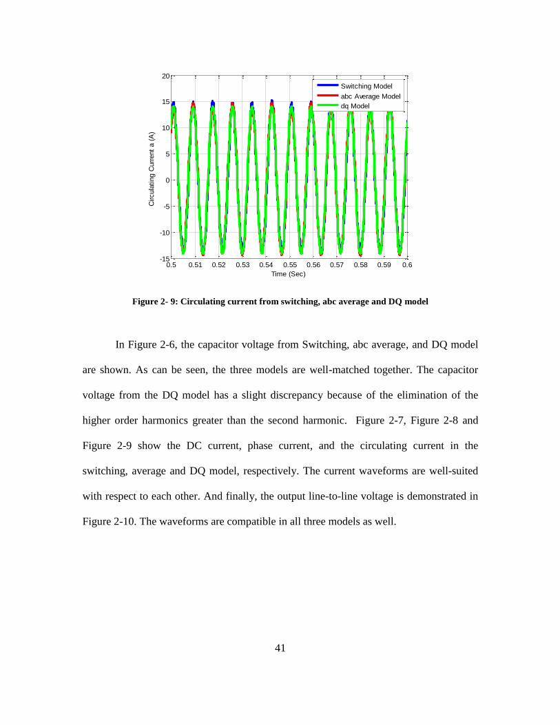
41
Figure 2- 9: Circulating current from switching, abc average and DQ model
In Figure 2-6, the capacitor voltage from Switching, abc average, and DQ model
are shown. As can be seen, the three models are well-matched together. The capacitor
voltage from the DQ model has a slight discrepancy because of the elimination of the
higher order harmonics greater than the second harmonic. Figure 2-7, Figure 2-8 and
Figure 2-9 show the DC current, phase current, and the circulating current in the
switching, average and DQ model, respectively. The current waveforms are well-suited
with respect to each other. And finally, the output line-to-line voltage is demonstrated in
Figure 2-10. The waveforms are compatible in all three models as well.
0.5 0.51 0.52 0.53 0.54 0.55 0.56 0.57 0.58 0.59 0.6-15
-10
-5
0
5
10
15
20
Time (Sec)
Circula
ting C
urr
ent
a (
A)
Switching Model
abc Average Model
dq Model

42
Figure 2- 10: MMC DC, phase, and circulating current from switching, abc average and DQ model
Figure 2- 11: Open loop transfer function of output current to duty cycle in DQ.
Once we have the DQ model, using linearization tools, such as the MATLAB
linearization tool, the model can be linearized and the open loop transfer functions can be
extracted. In Figure 2-11, the open loop transfer function of the output current to duty
0.5 0.51 0.52 0.53 0.54 0.55 0.56 0.57 0.58 0.59 0.6-3000
-2000
-1000
0
1000
2000
3000
Time (Sec)
Outp
ut
VLL (
V)
Switching Model
abc Average Model
dq Model
-50
0
50
100
To:
iq
100
101
102
103
104
105
-180
-90
0
To:
iq
From: Dq
100
101
102
103
104
105
Bode Diagram
Frequency (Hz)
Magnitude (
dB
) ;
Phase (
deg)
-100
-50
0
50
To:
id
From: Dd
-180
-90
0
To:
id
idq/Ddq
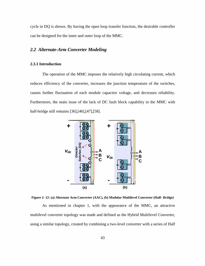
43
cycle in DQ is shown. By having the open loop transfer function, the desirable controller
can be designed for the inner and outer loop of the MMC.
2.2 Alternate-Arm Converter Modeling
2.3.1 Introduction
The operation of the MMC imposes the relatively high circulating current, which
reduces efficiency of the converter, increases the junction temperature of the switches,
causes further fluctuation of each module capacitor voltage, and decreases reliability.
Furthermore, the main issue of the lack of DC fault block capability in the MMC with
half-bridge still remains [36],[46],[47],[58].
ABC
+
-
vdc
+
-
vdc ABC
(a) (b)
Dir
ecto
r S
wit
ches (
DS
)
Figure 2- 12: (a) Alternate Arm Converter (AAC), (b) Modular Multilevel Converter (Half- Bridge)
As mentioned in chapter 1, with the appearance of the MMC, an attractive
multilevel converter topology was made and defined as the Hybrid Multilevel Converter,
using a similar topology, created by combining a two-level converter with a series of Half
44
or Full-Bridge or Power Electronic Building Blocks (PEBB) [36]. After the AAC
introduced by Alstom in 2010, several research projects have been carried out involving
the operation and control of the converter [23]. In [29], some interesting innovative
concepts for creating the novel Hybrid Multilevel Converters are presented. A 24MW
level VSC converter to evaluate different hybrid multilevel topologies from Alstom Grid
is studied in [59]. Also, an overview of the Modular Multilevel Converters for HVDC
applications is done in [60]. As is mentioned in chapter 1, an Alternate Arm Converter
(AAC) can be realized by adding a two-level voltage converter and awave-shaping circuit
on the DC side [23]. The structure is very similar to the Modular Multilevel Converter
(MMC), which makes the operation of the AAC similar to the MMC, with the exception
that it has switches to alternate the load power between upper arm and lower arm. Figure
2-12 shows the AAC and MMC configurations. As can be seen, the AAC has a series of
switches called Director Switches (DS) to alternate the arm current between upper and
lower arm. The main advantage of the AAC over the MMC is the capability of DC-Fault
ride-through and operation as a STATCOM after DC fault [61]. In Chapter 5, DC fault
ride-through of the AAC will be discussed elaboratley. In this section, first the operation
principle of the AAC will be explained and then the switching model and average model
of the AAC will be discussed.
2.3.2 Alternate Arm Converter (AAC) Operation Principles
In Figure 2-13, the single phase schematic of the AAC is shown. AAC consists of
the upper and lower arm Cascaded H-Bridges which provide the wave-shaping circuits.
The director switches include IGBTs connected in series in order to withstand the
45
maximum voltage which could be applied across the director switch when it is in the
open state.
To provide a sinusoidal voltage, the wave-shaping cascaded–bridge converter
should produce the voltage as shown in the Figure 2-13. For standard operation, the three
phase-legs operate in the same fashion with phase-legs ‘b’ and ‘c,’ lagging leg ‘a’ by
120° and 240°, respectively. Taking one phase-leg as an example, in the “upper arm
active” converter operation state, the upper arm is responsible for synthesizing positive
voltages at the converter AC voltage terminal by modulating the upper arm modules
when the upper arm director switch is closed. During the “lower arm active state”,
negative converter voltages are synthesized by modulating the lower arm modules when
the lower arm director switch is closed. During these two states, the upper and lower arm
director switches act as a complementary pair. An additional state, named “overlap”, is
used between the two aforementioned states in which both the upper and lower arm
director switches are closed, allowing a current that is common to the two arms to flow.
This current can be controlled to aid in the capacitor voltage balancing of the modules by
modulating the upper and lower arms’ power modules appropriately. The overlap time
existence principle and control will be discussed in the next chapters.

46
CellPos
Neg
am
Cell
Cell
Cell
Cell
Cell
Cell
Cell
Upper Arm
Lower Arm
vU
vL
+0.5Vdc
–0.5Vdc
vam
CHB1
CHB2
Direction Switches (DS Lower)
Direction Switches (DS Upper)
iua
ila
S1 S2
S3 S4
iSM
USM
UCC
O t
+0.5Vdc
+ Vdc
O t
+0.5Vdc
+Vdc
+0.5Vdc
–0.5Vdc
vam_ref
O t
DS Upper ONDS Lower Off
DS Lower ONDS Upper Off
vuA_ref
vlA_ref
Figure 2- 13: Basic operation of the AAC
One of the features of the AAC is that the module of the AAC should be in full-
bridge to provide the operation of the AAC in the so-called sweet-spot [61]. As will be
shown later, in the sweet spot, the energy between the DC side and the AC side are
balanced and the control efforts to balance the capacitor voltage will be easier.
2.3.3 AAC Voltage and Current Specifications
According to Figure 2-13, in order to have a sinusoidal output voltage, the upper
and lower arm full-bridge stacks voltage references should be as follows:
2sin22
)(
0sin22
)(
tiftV
mV
tV
tiftV
mV
tV
dcdclA
dcdcuA
(2-55)
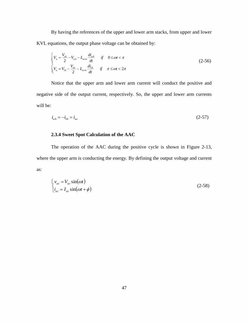
47
By having the references of the upper and lower arm stacks, from upper and lower
KVL equations, the output phase voltage can be obtained by:
22
02
tifdt
diL
VVV
tifdt
diLV
VV
lAarm
dclAa
uAarmuA
dca
(2-56)
Notice that the upper arm and lower arm current will conduct the positive and
negative side of the output current, respectively. So, the upper and lower arm currents
will be:
aclAuA iii (2-57)
2.3.4 Sweet Spot Calculation of the AAC
The operation of the AAC during the positive cycle is shown in Figure 2-13,
where the upper arm is conducting the energy. By defining the output voltage and current
as:
tIi
tVv
acac
acac
sin
sin (2-58)
48
A
2
aci
aci
dcV
uAV
A
2
aci
dcV
lAV
aci
Figure 2- 14 Single phase AAC operation in positive and negative cycles
The DC-side energy equation can be written:
2
cos
2
2
0
TIVEdti
VE acdc
DCac
T
dcDC (2-59)
Where the current in the DC side will be the load current as shown in Figure 2-14.
The AC side energy equation can be found:
4
)cos(2
0
TIVEdtivE acac
ACac
T
acAC
(2-60)
In order to have balanced energy during the half line frequency cycle, the input
and output energy should be equal. By equalizing the energy equations, the modulation
index to have balanced energy during the half of line frequency cycle can be obtained:
dcac
acacacdc
ACDC VVTIVTIV
EE
2
4
)cos(
2
cos (2-61)
Equation (2-61) provides the modulation index to be in the over-modulation
region as is shown in (2-62):

49
273.14
2
4
M
VV dc
ac (2-62)
From the above equation, we discover that to have balanced energy during the
operation of the upper and lower arm, the converter should have a modulation index of
4 . As the result, the upper and lower arm modules of the AAC should be Full-Bridge
to make the negative voltage possible over the stack.
2.3.5 AAC Switching Modeling
This section describes the derivation of the mathematical switching model of the
AAC. A simple three-phase AAC circuit with DC-link filter and one full-bridge power
module per arm is shown in Figure 2-15, where the converter is connected to the AC grid.
vSa
SUa1
am
SUa2
vCUa
iUa
ia
iLa
idc
n
vSb vSc
ib ic
+0.5Vdc
‒0.5Vdc
L
L
C
SLa∙vCLa
SUa∙vCUa
SUa3
SUa4
Ph
ase
b
Ph
ase
c
SLb1
SLb2
vCLaCSLb3
SLb4
SDSUa
SDSLa
CfVdc
Lf
Rf
Lf
Rf
Director
Switches
Figure 2- 15: AAC with one module in each arm
Since the AAC has full-bridge power cells with four power switches, the H-bridge
switches are modeled using a converter transfer function featuring three states –1,0,1.
The director switch, modeled as a conventional switching function 0,1, turns off at zero

50
current with appropriate control. Since operation of the AAC provides relatively high
ripple on DC current [62], the DC-link of the converter is connected to a DC-link filter,
which provides the interface to the DC-grid. For modeling simplicity, the DC-grid is
assumed to be a locally connected stiff voltage source. A state-space model of the AAC
can be derived by taking the arm inductor currents, DC-link filter inductor current, and
module capacitor voltages as states. The voltage across the part of the DC-link filter in
series with the DC-line, vf, is given by (2-63) or (2-64). Equating (2-63) and (2-64)
obtains (2-65), which is the filter inductor current, iLf, state-space equation, where Rf is
the filter resistance, Lf is the filter inductance, and IDCg is the DC-grid current.
Lfff idt
dLV (2-63)
fLfDCgf RiiV (2-64)
f
DCgf
f
Lff
LfL
iR
L
iRi
dt
d (2-65)
The three phase upper arm inductor current state-space equations can be derived
by taking a KVL loop from the DC-grid midpoint to the AC-grid neutral via an upper arm
and then directly back to the DC-grid midpoint as shown in (2-66), where L is the arm
inductance, VDCg is the DC-grid voltage, vDSUx is the voltage across an upper arm’s
director switch, vSx is the phase supply voltage, and vnm is the DC-grid midpoint to AC-
grid neutral voltage. Similarly, (2-67) gives the three lower arm inductor current state-
space equations, where vDSLx is the voltage across a lower arm director switch.
nmSxDSUx
n
i
UxiUxiLff
DCgDSUxUx vvvvSi
dt
dL
V
L
Si
dt
d
12 (2-66)

51
nmSxDSLx
n
i
LxiLxiLff
DCgDSLxLx vvvvSi
dt
dL
V
L
Si
dt
d
12 (2-67)
The voltages across the upper (vDSUx) and lower (vDSLx) arm director switches
can be defined by (2-68) and (2-69) respectively, by applying KVL to the loop around the
DC-grid and a phase-leg, and noting that when a director switch is closed, the voltage
across it is zero.
n
i
LxiLxiLxDSLxUx
n
i
UxiUxiLffDCgDSUxDSUx vSidt
dLvi
dt
dLvSi
dt
dLVSv
11
2)1( (2-68)
n
i
LxiLxiLxDSUxUx
n
i
UxiUxiLffDCgDSLxDSLx vSidt
dLvi
dt
dLvSi
dt
dLVSv
11
2)1( (2-69)
Substituting (2-69) into (2-68) allows the lower arm director switch voltage to be
eliminated from (2-68); consequently, (2-70) can be obtained. Similarly, for the lower
arm director switches, (2-71) can be obtained.
n
i
LxiLxiLxUx
n
i
UxiUxiLffDCgDSLx
n
i
LxiLxiLxUx
n
i
UxiUxiLffDCg
DSLxDSUxDSLxDSUx
DSUxDSUx
vSidt
dLi
dt
dLvSi
dt
dLVS
vSidt
dLi
dt
dLvSi
dt
dLV
SSSS
Sv
11
11
2)1(
2
)(
)1( (2-70)
n
i
LxiLxiLxUx
n
i
UxiUxiLffDCgDSUx
n
i
LxiLxiLxUx
n
i
UxiUxiLffDCg
DSLxDSUxDSLxDSUx
DSLxDSLx
vSidt
dLi
dt
dLvSi
dt
dLVS
vSidt
dLi
dt
dLvSi
dt
dLV
SSSS
Sv
11
11
2)1(
2
)(
)1( (2-71)
The DC-grid midpoint to AC-grid neutral voltage is given by (2-72).
cbax
DSLx
cbax
DSUx
cbax
n
i
LxiLxi
cbax
n
i
UxiUxinm vvvSvSv,,,,,, 1,, 16
1 (2-72)
The three-phase line current’s state-space equations are given by (2-73). By
making the state-space variable transformation [52], the three sum current, isumx, state-
space equations are given by (2-74).

52
nmSxDSLx
n
i
LxiLxiLff
DCg
DSLx
nmSxDSUx
n
i
UxiUxiLff
DCg
DSUx
x
vvvvSidt
dL
VS
vvvvSidt
dL
VS
Li
dt
d
1
1
2
21 (2-73)
nmSxDSLx
n
i
LxiLxiLff
DCg
DSLx
nmSxDSUx
n
i
UxiUxiLff
DCg
DSUx
sumx
vvvvSidt
dL
VS
vvvvSidt
dL
VS
Li
dt
d
1
1
2
21 (2-74)
As the converter DC-link current can be defined by (2-75), (2-76) can be written
by substituting (2-66) into (2-75) completing the model derivation for the AAC.
UcUbUadc iiii (2-75)
nmSxDSUx
n
i
UxiUxiLff
DCg
cbax
DSUxdc vvvvSidt
dL
VS
Li
dt
d
1,, 2
1 (2-76)
So the complete state-space model is given by (2-77).
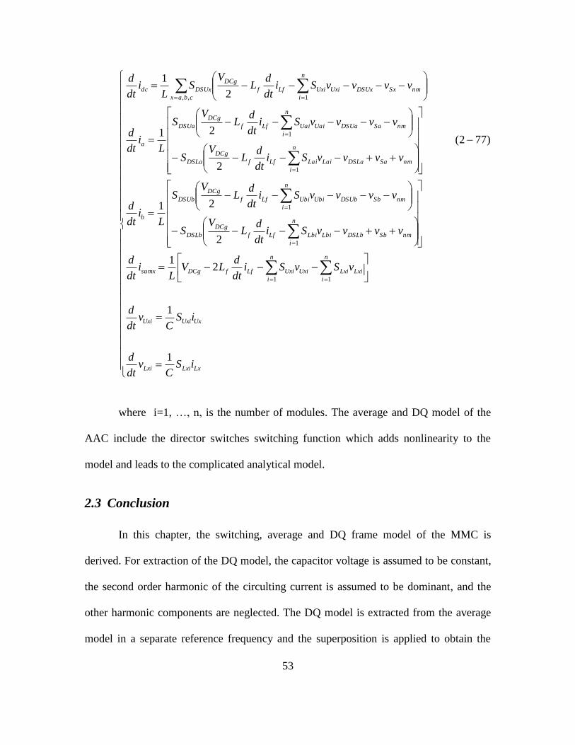
53
LxLxiLxi
UxUxiUxi
n
i
LxiLxi
n
i
UxiUxiLffDCgsumx
nmSbDSLb
n
i
LbiLbiLff
DCg
DSLb
nmSbDSUb
n
i
UbiUbiLff
DCg
DSUb
b
nmSaDSLa
n
i
LaiLaiLff
DCg
DSLa
nmSaDSUa
n
i
UaiUaiLff
DCg
DSUa
a
nmSxDSUx
n
i
UxiUxiLff
DCg
cbax
DSUxdc
iSC
vdt
d
iSC
vdt
d
vSvSidt
dLV
Li
dt
d
vvvvSidt
dL
VS
vvvvSidt
dL
VS
Li
dt
d
vvvvSidt
dL
VS
vvvvSidt
dL
VS
Li
dt
d
vvvvSidt
dL
VS
Li
dt
d
1
1
21
2
21
)772(
2
21
2
1
11
1
1
1
1
1,,
where i=1, …, n, is the number of modules. The average and DQ model of the
AAC include the director switches switching function which adds nonlinearity to the
model and leads to the complicated analytical model.
2.3 Conclusion
In this chapter, the switching, average and DQ frame model of the MMC is
derived. For extraction of the DQ model, the capacitor voltage is assumed to be constant,
the second order harmonic of the circulting current is assumed to be dominant, and the
other harmonic components are neglected. The DQ model is extracted from the average
model in a separate reference frequency and the superposition is applied to obtain the
54
final DQ model from different frequency references. Although the extracted model is
complicated in the DQ frame, by using the proposed DQ model, the design of the inner
and outer loop controller of the converter can be simplified. By implementing the
obtained model in a simulation software such as SIMULINK/MATLAB and using
linearzation tools, the bode diagram of the required transfer functions can be extracted for
converter control design purposes.
Furthermore, the AAC operation principles are discussed in this chapter. Since the
modeling of this converter is more complex than the MMC, the switching model of the
AAC is presented here, and further extraction of the DQ model leads to a very
complicated nonlinear model. During the “upper arm active” and “lower arm active”
states, the AAC line currents are controlled by the upper and lower arm modules
respectively. However, in the “overlap” state, the AAC shares very similar features to the
MMC. Hence, both the MMC and AAC at “overlap” have the same state equations for
the line currents. In both the MMC and AAC, the capacitors of the power modules act as
intermediate energy storage between the DC and AC terminals. Thus, to ensure a
balanced voltage operation among these capacitors, a zero net change requirement of
total stored energy must be enforced over a fundamental frequency period. The actual
power balance is achieved by the flowthrough of the sum current, which, along with DC
offset, is indispensable for both converters. However, the “overlap” states in the AAC
only occur in one phase-leg at a time, that is, only one phase-leg can have both director
switches on simultaneously. This is a fundamental difference with the MMC in terms of
circulating current, since the circulation of current between phase-legs, present in the

55
MMC, is not present in the AAC. This distinguishes the converters from each other in the
way that each can balance their capacitor voltages.
56
Chapter 3 Modular Multilevel Converters Control
3.1 Introduction
In this chapter, the arm balancing, module capacitors voltage balance, and closed
loop output power control associated with modular multilevel converters will be
discussed. The control method used in this work is based on Makoto Hagiwara and
Hirofumi Akagi’s arm balancing and output current control method [42],[63]. Based on
this method, the power cell capacitor’s voltage control of the modular multilevel
converters is divided into: the capacitor voltage average control or energy balancing,
individual capacitor voltage control, and arm-balancing control. The normal operation of
the MMC deals with internal even harmonics current, which circulates though the arms in
each phase. This circulating current causes more power losses and more ripple on
capacitor voltage. Since the MMC involves interaction between capacitor voltage and the
circulating current [46], the internal capacitor control should be equipped with circulating
current suppressing control. Using a circulating current controller can reduce the stress
over the capacitors as well as the arm current, which results in lower thermal stress
throughout the module components. Using circulating current suppressing control will
change the design process of the arm inductor. This will be discussed in the next chapter.
Many studies have been carried out to control and reduce the circulating current of the
converter. In [48], a reduced switching-frequency modulation method based on the

57
sorting algorithm by using a phase-shifted carrier is proposed. The circulating current
suppresion control in [48] is modeled and design in the DQ frame, where, due to the need
for PLL, it increases the complexity of the circuit. To avoid using PLL, the Circulating
Current Suppressing Control (CCSC) for the MMC is implemented using a Proportional-
Quasi-Resonant (PQR) controller, as described in [58]. In this thesis, the Proportional-
Quasi-Resonant (PQR) controller will be considered in the design of the CCSC for a
modular multilevel converter based on the same method proposed in [58]. To study the
circulating current, the following mathematical modeling of the MMC is performed.
Figure 3-1 shows the circuit schematic of the MMC under consideration, featuring N
power modules per phase-arm (positive and negative phase-arm within the phase-leg),
and 2N power modules per phase-leg. These power modules are connected in series as
shown in the figure, where in this case all power modules are constructed with half-
bridge circuits feeding a flying capacitor, although other configurations using a full-
bridge or alternative circuit configurations may be used as well, depending on the
application objectives and requirements.

58
Figure 3- 1: Modular Multilevel Converter topology with each power module structure
As shown in [46], the upper phase-arm and lower phase-arm currents contain
even order harmonics, with the second order component being the most significant one.
Per Figure 3-1, the upper and lower phase-arm currents are given by
)2sin()sin(23
2 tItII
I hadc
uA (3-1)
)2sin()sin(23
2 tItII
I hadc
lA (3-2)
Employing an average model for the half-bridge converter of the power module,
and neglecting the resistive voltage drop across each phase phase-arm, it follows that the
reference voltage waveforms for the upper and lower phase-arm modulation signals are:
tV
mV
V dcdcuAref sin
22 (3-3)
tV
mV
V dcdclAref sin
22 (3-4)

59
As such, when summing (3-3) and (3-4), which corresponds to measuring the
voltage from positive to negative rail, the AC component in these equations cancels out
leaving Vdc as the result of this sum. Likewise, and taking into consideration a 120
phase-shift between converter phase-legs, when the voltage between two different phases
is measured, the DC component (Vdc/2) cancels out, leaving only the AC term between
them.
In normalized terms, (3-3) and (3-4) may be rewritten as shown below, where NuA
and NlA correspond to the normalized voltage reference for each power module, which in
turn correspond to the average duty cycle of their respective half-bridge switching
function.
tmNuA sin2
1
2
1 (3-5)
tmN lA sin2
1
2
1 (3-6)
Accordingly, the average voltage of the power module capacitors for the upper
and lower phase-arms are given by:
tdINC
v uAuACu
1 (3-7)
tdINC
v lAlACl
1 (3-8)
The total average voltage of the MMC phase-leg is then given by:
dtiN
CtNdtiN
CtNVVV LalUaulAuAleg
1sin
2
1
2
11sin
2
1
2
1 (3-9)
The difference between the DC voltage component and the total voltage across
the phase-leg corresponds to the voltage across the phase-arm inductors, which is the
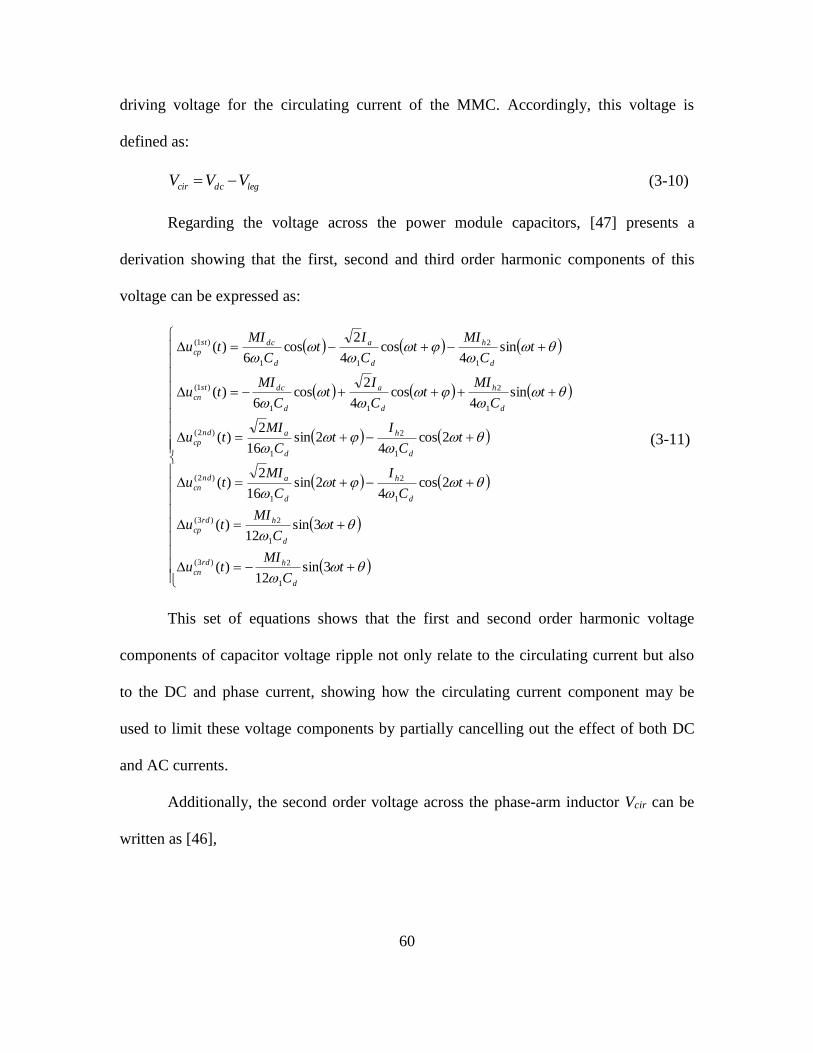
60
driving voltage for the circulating current of the MMC. Accordingly, this voltage is
defined as:
legdccir VVV (3-10)
Regarding the voltage across the power module capacitors, [47] presents a
derivation showing that the first, second and third order harmonic components of this
voltage can be expressed as:
tC
MItu
tC
MItu
tC
It
C
MItu
tC
It
C
MItu
tC
MIt
C
It
C
MItu
tC
MIt
C
It
C
MItu
d
hrd
cn
d
hrd
cp
d
h
d
and
cn
d
h
d
and
cp
d
h
d
a
d
dcst
cn
d
h
d
a
d
dcst
cp
3sin12
)(
3sin12
)(
2cos4
2sin16
2)(
2cos4
2sin16
2)(
sin4
cos4
2cos
6)(
sin4
cos4
2cos
6)(
1
2)3(
1
2)3(
1
2
1
)2(
1
2
1
)2(
1
2
11
)1(
1
2
11
)1(
(3-11)
This set of equations shows that the first and second order harmonic voltage
components of capacitor voltage ripple not only relate to the circulating current but also
to the DC and phase current, showing how the circulating current component may be
used to limit these voltage components by partially cancelling out the effect of both DC
and AC currents.
Additionally, the second order voltage across the phase-arm inductor Vcir can be
written as [46],
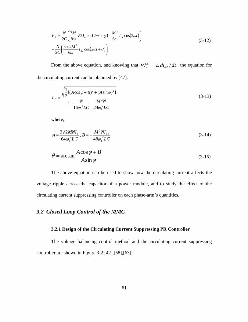
61
tIM
C
N
tIM
tIM
C
NV
h
dcacir
2cos6
23
2
2cos6
2cos28
3
2
2
2
2
(3-12)
From the above equation, and knowing that dtdiLV hh 2
)2(
2 , the equation for
the circulating current can be obtained by [47]:
LC
NM
LC
N
ABA
Ih
2
1
2
2
1
22
2
24161
])sin()cos[(2
1
(3-13)
where,
LC
NIMB
LC
MNIA dca
2
1
2
2
1 48,
64
23
(3-14)
sin
cosarctan
A
BA (3-15)
The above equation can be used to show how the circulating current affects the
voltage ripple across the capacitor of a power module, and to study the effect of the
circulating current suppressing controller on each phase-arm’s quantities.
3.2 Closed Loop Control of the MMC
3.2.1 Design of the Circulating Current Suppressing PR Controller
The voltage balancing control method and the circulating current suppressing
controller are shown in Figure 3-2 [42],[58],[63].
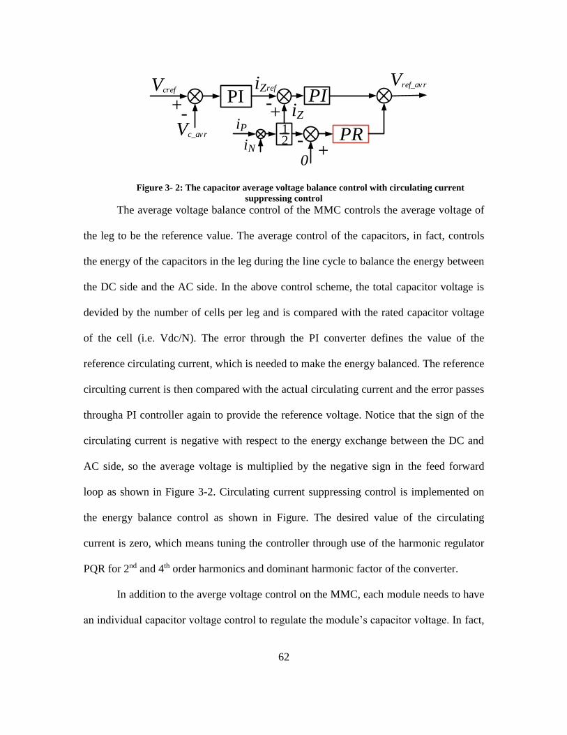
62
-
Vcref
Vc_avr
+
Vref_av r
PI -+
iZref
iP
iN
PI
12
iZ
PR-+
0
Figure 3- 2: The capacitor average voltage balance control with circulating current
suppressing control
The average voltage balance control of the MMC controls the average voltage of
the leg to be the reference value. The average control of the capacitors, in fact, controls
the energy of the capacitors in the leg during the line cycle to balance the energy between
the DC side and the AC side. In the above control scheme, the total capacitor voltage is
devided by the number of cells per leg and is compared with the rated capacitor voltage
of the cell (i.e. Vdc/N). The error through the PI converter defines the value of the
reference circulating current, which is needed to make the energy balanced. The reference
circulting current is then compared with the actual circulating current and the error passes
througha PI controller again to provide the reference voltage. Notice that the sign of the
circulating current is negative with respect to the energy exchange between the DC and
AC side, so the average voltage is multiplied by the negative sign in the feed forward
loop as shown in Figure 3-2. Circulating current suppressing control is implemented on
the energy balance control as shown in Figure. The desired value of the circulating
current is zero, which means tuning the controller through use of the harmonic regulator
PQR for 2nd and 4th order harmonics and dominant harmonic factor of the converter.
In addition to the averge voltage control on the MMC, each module needs to have
an individual capacitor voltage control to regulate the module’s capacitor voltage. In fact,

63
the individual capacitor voltage can be replaced by the simple sorting alghorithm, which
is used throughout the literature [43]. Figure 3-3 shows the individual capacitor voltage
control for the MMC.
+1:ip, iN>0
-1:ip, iN<0-
Vcref
vcj
+vref_j
K ±1
Figure 3- 3: Individual cell capacitor voltage balance control
Individual capacitor voltage control measures the actual value of the capacitors in
each cell and it compares that value with the rated value. Through the proportional
controller and, depending on the arm current direction, it tunes the controller such that the
voltage balance reaches each cell. Using this scheme, the reference voltage for each
power module is given by adding the output current reference, the reference achieved by
the capacitor average control, and the individual capacitor voltage balance control:
NArefjrefavrreflowref
PArefjrefavrrefupref
vvvv
vvvv
____
____
(3-16)
A Proportional Quasi-Resonant (PQR) controller is used as a Circulating Current
Suppressing Controller (CCSC) as was mentioned before, with the structure shown
below.
2
02
2
22
2
01
2
11
)4(2
2
)2(2
2
ss
sK
ss
sKKG
c
bc
c
bcpQPR
(3-17)
This controller is used to regulate specific harmonics of a given signal. In the case
of the MMC, when controlling the circulating current, the second and the fourth order
harmonics are the most significant ones, hence the controller is tuned to these two
components. The parameters of the controller are designed for at least 20dB gain on the

64
tuned harmonics. The MMC circuit parameters used for the design of the controllers is
described in Table 3-1. The parameters of the controller are designed to provide the
corresponding gain are shown in Table 3-2. The Bode plot of the controller is shown in
Figure 3-4. As shown, the resonant frequencies correspond to 120 Hz and 240 Hz.
Table 3- 1: MMC parameters values for closed-loop control simulation
Output Frequency 60 Hz
Switching Frequency 540 Hz
L 3.7 mH
C 4000µF
Ri 0.004Ω
Modulation Index m 0.9
Output Voltage 6kV L-L
P 3MW
Voltage Over each Module 1kV
DC Bus Voltage 10 kV
Number of Module per arm 10
Table 3- 2: The CCSC controller parameters
0 60Hz
1c 10Hz
2c 10Hz
1bK 10
2bK 10
pK 1

65
Figure 3- 4: Bode plot of the circulating current suppressing Proportional Quasi Resonant (PQR)
controller
In order to show the circulating current suppressing controller at work and gauge
its impact, simulations using the model developed are conducted. In Figure 3-5, the upper
phase-arm current harmonic contents are shown. The harmonic analysis for the upper
phase-arm current, the capacitor voltage ripple, as well as the output voltage and current
is then performed when the Circulating Current Suppressing Controller (CCSC) is active.
The results are compared to the case without the controller and shown in Table 3-3,
which illustrates the positive impact that this controller has on all converter variables,
with only a slight increase in the converter output’s current distortion. Specifically, both
the capacitor voltage and current improved their harmonic distortion, translating to lower
losses and less voltage stress for the IGBTs of the power module. The phase-arm current
also saw its distortion diminished, resulting in lower thermal stress for all IGBT and
capacitors in the converter structure.
0
5
10
15
20
25
Magnitude (
dB
)
100
101
102
103
104
-90
-45
0
45
90
Phase (
deg)
Bode Diagram
Frequency (Hz)
G_QPR
120 Hz 240Hz
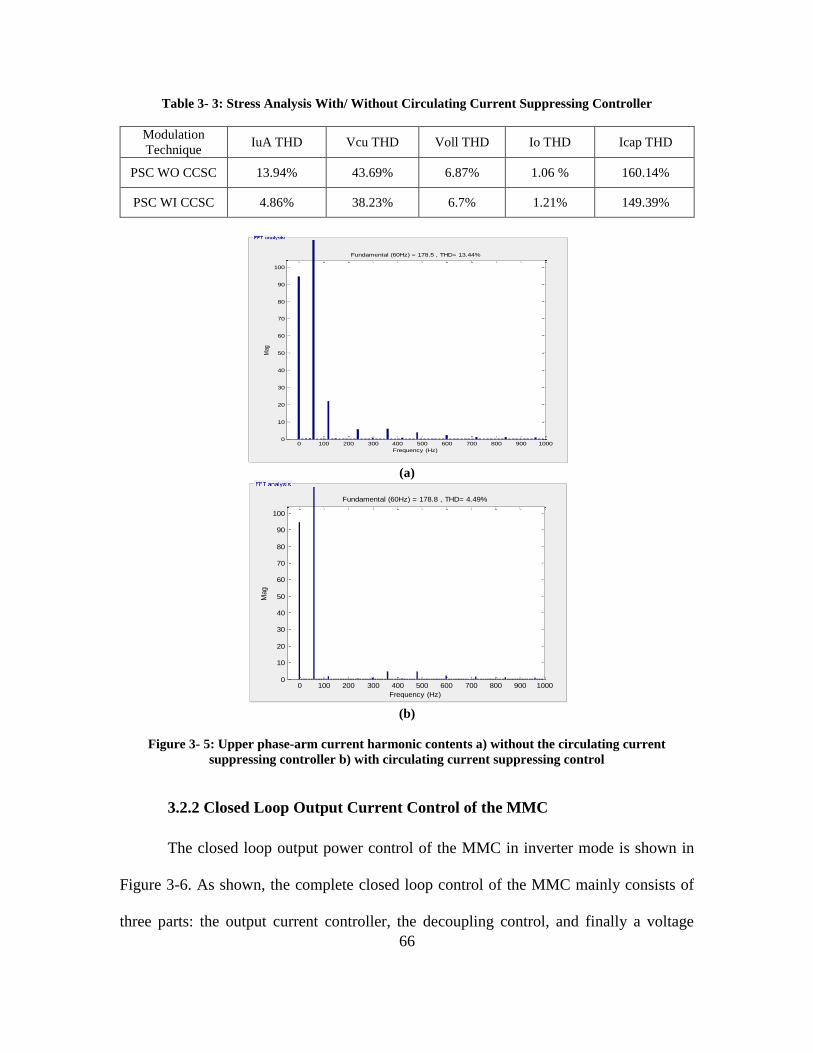
66
Table 3- 3: Stress Analysis With/ Without Circulating Current Suppressing Controller
Modulation
Technique IuA THD Vcu THD Voll THD Io THD Icap THD
PSC WO CCSC 13.94% 43.69% 6.87% 1.06 % 160.14%
PSC WI CCSC 4.86% 38.23% 6.7% 1.21% 149.39%
(a)
(b)
Figure 3- 5: Upper phase-arm current harmonic contents a) without the circulating current
suppressing controller b) with circulating current suppressing control
3.2.2 Closed Loop Output Current Control of the MMC
The closed loop output power control of the MMC in inverter mode is shown in
Figure 3-6. As shown, the complete closed loop control of the MMC mainly consists of
three parts: the output current controller, the decoupling control, and finally a voltage
0.3 0.31 0.32 0.33 0.34 0.35 0.36
-50
0
50
100
150
200
250
FFT window: 4 of 24 cycles of selected signal
Time (s)
0 100 200 300 400 500 600 700 800 900 10000
10
20
30
40
50
60
70
80
90
100
Frequency (Hz)
Fundamental (60Hz) = 178.5 , THD= 13.44%
Mag
0.3 0.31 0.32 0.33 0.34 0.35 0.36 0.37 0.38 0.39
0
100
200
FFT window: 6 of 24 cycles of selected signal
Time (s)
0 100 200 300 400 500 600 700 800 900 10000
10
20
30
40
50
60
70
80
90
100
Frequency (Hz)
Fundamental (60Hz) = 178.8 , THD= 4.49%
Mag
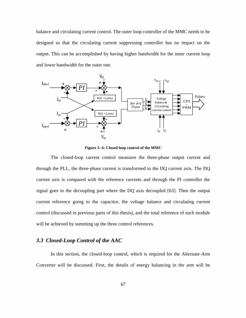
67
balance and circulating current control. The outer loop controller of the MMC needs to be
designed so that the circulating current suppressing controller has no impact on the
output. This can be accomplished by having higher bandwidth for the inner current loop
and lower bandwidth for the outer one.
-
+
+
-
PI
PI
W(L+Larm)
+-
-+
+
-
Va
Vb
Vc
CPS-
PWM
Pulses
Isdref
Isqref
IsdInv d-qTrans
vPjk vNjk
Voltage
balance &
Circulating
current control
iPjiNj
Vsd
Vsq
Isq W(L+Larm)
Figure 3- 6: Closed loop control of the MMC
The closed-loop current control measures the three-phase output current and
through the PLL, the three-phase current is transformed to the DQ current axis. The DQ
current axis is compared with the reference currents and through the PI controller the
signal goes to the decoupling part where the DQ axis decoupled [63]. Then the output
current reference going to the capacitor, the voltage balance and circulating current
control (discussed in previous parts of this thesis), and the total reference of each module
will be achieved by summing up the three control references.
3.3 Closed-Loop Control of the AAC
In this section, the closed-loop control, which is required for the Alternate-Arm
Converter will be discussed. First, the details of energy balancing in the arm will be
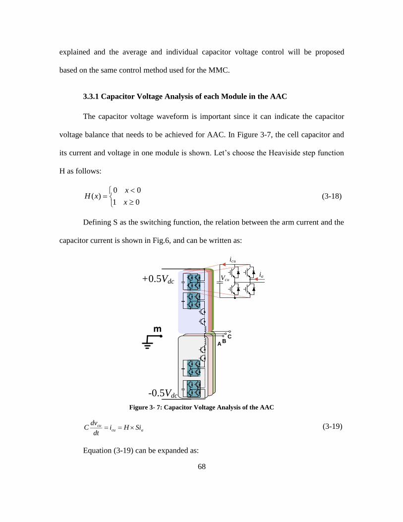
68
explained and the average and individual capacitor voltage control will be proposed
based on the same control method used for the MMC.
3.3.1 Capacitor Voltage Analysis of each Module in the AAC
The capacitor voltage waveform is important since it can indicate the capacitor
voltage balance that needs to be achieved for AAC. In Figure 3-7, the cell capacitor and
its current and voltage in one module is shown. Let’s choose the Heaviside step function
H as follows:
01
00)(
x
xxH (3-18)
Defining S as the switching function, the relation between the arm current and the
capacitor current is shown in Fig.6, and can be written as:
AB
C
m
+0.5Vdc
-0.5Vdc
Vcu
icu
ia
Figure 3- 7: Capacitor Voltage Analysis of the AAC
acucu SiHi
dt
dvC (3-19)
Equation (3-19) can be expanded as:

69
tMttHI
dt
dvC
tItM
tH
tIttHM
tH
mcu
m
m
2cossin)(sin2
sinsin22
1)(sin
sinsin)(sin22
1)(sin
(3-20)
By taking the integral from (3-20) from t0 , the capacitor voltage ripple
can be obtained by:
tttMC
Iv m
cu 0cos2sin4
(3-21)
Figure 3- 8: Capacitor voltage ripple in different load power factors
Equation (3-21) finds the capacitor waveform in different load power factors in
the half-line frequency. The capacitor voltage ripple is shown in Figure 3-8. It can be
inferred that the capacitor voltage ripple in inductive loads needs to be balanced at the
half-line frequency cycle. This can be achieved by introducing overlap time between
director switches.
0 1 2 3 4 5 6 7 8
x 10-3
-60
-50
-40
-30
-20
-10
0
10
20
Time(sec)
Cap V
oltage R
ipple
(V
)
phi=0
phi=pi/6
phi=pi/3
phi=90

70
3.3.2 Capacitor Voltage Balance Control and Energy Balance Control
Schemes
From Figure 3-8, it can be deduced that the capacitor voltage of the AAC needs to
be balanced during the half-of-line frequency. This can be achieved by introducing
overlap time between the upper and lower arm DS. Introducing overlap time provides
energy balance between each module and DC-side. During the overlap time, all the
capacitors will be inserted and the output voltage will be about zero. In Figure 3-9, upper
and lower arm voltage references are shown in the presence of the overlap time. This
overlap time is controlled by the control system to provide appropriate overlap time
between the upper and lower arms. Another function of the overlap time is to provide the
zero current switching condition for the DS in order to minimize stress voltage due to
turning off the switch in the inductive loads. The ZCS operation of the DS switch will be
discussed later. The control schemes for the AAC will be explained in the following
subsections:
3.3.3 Overlap Time Control of the AAC
The required overlap time between the upper arm and the lower arm can be
achieved by the control scheme shown in Figure 3-10. In this control scheme, Uz, the
output of the controller, shows the average voltage which is required to charge the
capacitor to the reference value. The value of the overlap time can be found by solving
following equation:
21
2
1
)sin(
)sin(ovovOV
zovm
zovmttT
UtV
UtV
(3-22)
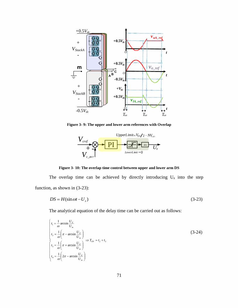
71
AB
C
m
+0.5Vdc
-0.5Vdc
+
VStackA
-
+
VStackB
-
O t
+0.5Vdc
vuA_ref
O t
+0.5Vdc
+Vdc
vlA_ref
Ot
+0.5Vdc
-0.5Vdc
vo_ref
ovT ovTovT
Figure 3- 9: The upper and lower arm references with Overlap
-
Vcref
Vc_avr
+PI Uz
abs
Cel lNVUpperLimit 2
0LowerLimit
DCV
Figure 3- 10: The overlap time control between upper and lower arm DS
The overlap time can be achieved by directly introducing Uz into the step
function, as shown in (3-23):
)(sin zUtHDS (3-23)
The analytical equation of the delay time can be carried out as follows:
32
4
3
2
1
arcsin21
arcsin1
arcsin1
arcsin1
ttT
U
Ut
U
Ut
U
Ut
U
Ut
OV
m
Z
m
Z
m
Z
m
Z
(3-24)

72
3.3.4 Individual Capacitor Voltage Control of the AAC
The proposed method in this work for the capacitor balance control takes the
control schemes of reference [42] for the MMC and applies the same concept to the AAC
first instead of using a sorting algorithm. The individual capacitor voltage control is
shown in Figure 3-11. The controller used is PI in order to make the DC error as small as
possible.
-
Vcref
vcj
+PI ±1 v
ref_j
0:1
0:1
,
,
LU
LU
ii
ii
Figure 3- 11: Individual capacitor voltage control
The reference voltage from this controller will be added to the reference voltage
of the upper and lower arm to make the final reference of the upper and lower stack
voltages. The final reference can be obtained thusly:
lArefjreflowref
uArefjrefupref
vvv
vvv
___
___
(3-25)
Where, uArefv _ and lArefv _ are given from the output current control.
3.2.5 Closed-loop Output Current control of the AAC
A similar control scheme for the MMC shown in Figure 3-6 can be utilized for the
AAC. The output current measurements are transformed to the DQ axis current and the
values are compared with the reference DQ axis current. The signals are then fed through
the PI controller to the decoupling control to obtain the reference DQ voltages. The
reference voltages in DQ are transformed in three-phase form and the references will be
73
added by the individual capacitor voltage balance to obtain the reference signals for the
modulation. The overlap time control signal will be used prior to the modulation stage to
form the desired reference signals for the upper and lower arm as shown in Figure 3-9.
The carrier phase shift modulation technique is used to modulate reference waveforms to
the PWM signals. In the next chapter, more details on the operations of the AAC and the
overlap time will be discussed.
3.4 Conclusion
Chapter 3 describes the closed-loop control scheme, which is used to operate the
modular multilevel converters. The implemented control method is based on average and
individual capacitor votage control, supplied with the Circulating Current Suppressing
Control (CCSC), and using Proportional Quasi-Resonant (PQR) tuned for the most
dominant circulating current harmonics (i.e. 2nd and 4th) order harmonics. Moreover, The
Output current closed-loop control in DQ reference is provided for both the MMC and
the AAC. AAC also requires overlap time control for its operation and energy balancing
of the arm. The similar control method expanded for the AAC features individual
capacitor voltage balance and overlap time control and the same output control method.
In the next chapters, the closed-loop control discussed here will be used to provide
further analysis of the modular multilevel converters in terms of design considerations
and DC fault ride-through capability.

74
Chapter 4 Modular Multilevel Converters Design
Considerations
4.1 Introduction
This chapter describes the specific design considerations of modular multilevel
converters. Since the size of the DC-link distributed capacitor in each cell is relatively
high so as to reduce the voltage ripple over in each module, and there are usually a high
number of power cells, the capacitor bank should be carefully designed to provide overall
high reliability for the converter. The reliabiltiy-oriented design of the capacitor bank for
the modular multilevel converter will be studied in this chapter. The comparison among
different modulation techniques for the modular multilevel converter will be performed
and, moreover, the design of the each module capacitor bank size and the arm inductor
will be explained. The modular multilevel converter’s switching frequncy is usually
selected to be low to avoid semiconductor losses and increase the efficiency of the
converter. Furthermore, the equivalent switching frequency is interleaved by the number
of cells and the equivalnet switching will be higher than each power cell’s switching
frequency. To design the switching frequency, a balance should be achieved between the
semiconductor losses and the capacitor voltage ripple in each cell since the switching
frequency decreases as the capacitor voltage ripple increases. This chapter will present a

75
reliability-oriented switching frequency analysis for the modular multilevel converter
with half-bridge power cells.
There is different design requirement for the Alternate Arm Converter (AAC)
since the operation principles are totally different than those of the MMC. This chapter
will discuss design of the number of the power cells, Director Switches, capacitor bank,
and the arm inductor and will illustrate the Zero Current Switching operation of the AAC
by selecting the appropriate size of the arm inductor. Finally, a comparison between the
MMC and AAC in terms of the semiconductor losses and size will be performed in this
chapter.
4.2 High Reliability Capacitor Bank Design for Modular Multilevel
Converters
In Figure 4-1, the failure cause distribution over a power electronics converter
component is shown [64]. As shown, capacitors are the most susceptible elements to
failure among the various components. The number and ratio of the capacitors can be
even higher when there is need for a high energy storage in the converter especially in
modular structure converters. Capacitors play an important role in the operation of the
converter. One of the MMC’s issues is the large number of high-power capacitors that
should be placed in each module, especially in high-power applications. This high
number of capacitors can cause complexity and reliability problems and can restrict the
lifetime of the converter [49]. Also, design of the capacitor bank and its effect on the
other parameters design needs to be carefully studied. Several studies have addressed the
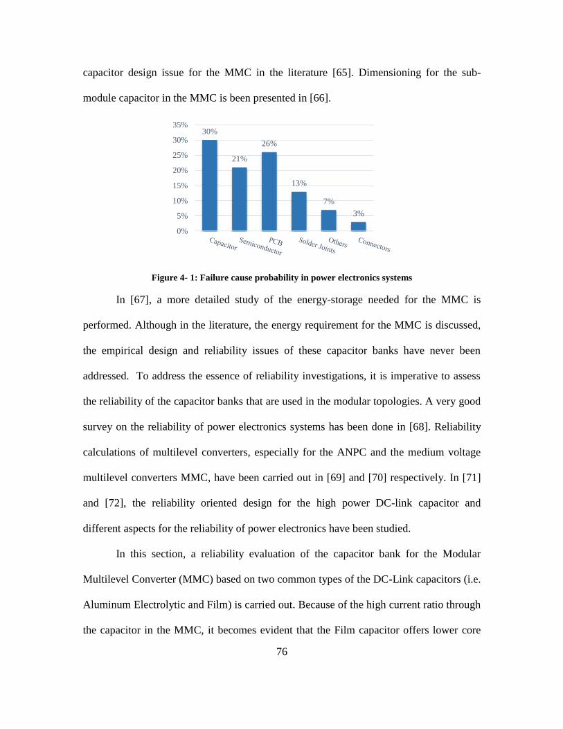
76
capacitor design issue for the MMC in the literature [65]. Dimensioning for the sub-
module capacitor in the MMC is been presented in [66].
Figure 4- 1: Failure cause probability in power electronics systems
In [67], a more detailed study of the energy-storage needed for the MMC is
performed. Although in the literature, the energy requirement for the MMC is discussed,
the empirical design and reliability issues of these capacitor banks have never been
addressed. To address the essence of reliability investigations, it is imperative to assess
the reliability of the capacitor banks that are used in the modular topologies. A very good
survey on the reliability of power electronics systems has been done in [68]. Reliability
calculations of multilevel converters, especially for the ANPC and the medium voltage
multilevel converters MMC, have been carried out in [69] and [70] respectively. In [71]
and [72], the reliability oriented design for the high power DC-link capacitor and
different aspects for the reliability of power electronics have been studied.
In this section, a reliability evaluation of the capacitor bank for the Modular
Multilevel Converter (MMC) based on two common types of the DC-Link capacitors (i.e.
Aluminum Electrolytic and Film) is carried out. Because of the high current ratio through
the capacitor in the MMC, it becomes evident that the Film capacitor offers lower core
30%
21%
26%
13%
7%
3%
0%
5%
10%
15%
20%
25%
30%
35%

77
temperature increases than Aluminum Electrolytic Capacitors due to the low ESR and
power loss. Case studies for the reliability function were carried out based on three
sample designs using ALE and Film capacitors. The results show that the Film capacitor
bank design offers the highest reliability and the longest life solution in each design. In
order to improve lifetime and reliability of the Aluminum Electrolytic Capacitor, adding
a Film Capacitor to the ALE capacitor bank is presented as a viable option. Reliability
modeling of the capacitor bank for the Modular Multilevel Converters (MMC) based on
the Markov State-Space Model (MSSM) was also carried out and then, using a case
study, the reliability of the capacitor bank is evaluated considering both Aluminum
Electrolytic (ALE) Capacitor Bank (CB) and Film CB designs. Furthermore, the
comparison among the reliability modeling methods (i.e. Part-Count, Combinatorial and
Markov Model) was carried out and shows that the Markov Model result is expected to
be more accurate and to have more useful results compared to other reliability models, as
it considers the fault tolerance and redundancy for the capacitor bank.
4.2.1 Capacitor Bank Size Design in Modular Multilevel Converter
Considering the average model and negligible voltage over each arm resistance as
presented in Chapter 2, the equation for the reference of the upper arm and lower arm
modulation signal can be obtained as follows:
tV
mV
V dcdcuA sin
22 (4-1)
tV
mV
V dcdclA sin
22 (4-2)

78
The upper and lower arm currents have three-significant elements: DC current,
phase current, and even order harmonics circulating current, shown as follows:
n
h
hadc
uA itII
I2
2
)sin(23
(4-3)
n
h
hadc
lA itII
I2
2
)sin(23
(4-4)
Where, h=2n and n=1… ∞. Considering the ESR for the practical floating DC-
Link capacitor, the voltage across the sub-module capacitor bank in the upper arm is:
cucucu irivdt
dC )( (4-5)
Where, cui is the current through the capacitor bank and r is the ESR. The current
through the capacitor can be obtained using the following equation:
uAuAcu INi (4-6)
By replacing the modulation signal equation for the upper arm, the current
through the capacitor is calculated by:
n
h
hadc
cu itII
tm
i2
2
)sin(23
sin22
1
(4-7)
And the voltage across the capacitor bank can be extracted by solving the
differential equation:
CuCuCuCu ritdiC
vv
1)0( (4-8)
)sin(23
sin22
1
)sin(23
sin22
11)0(
2
2
2
2
n
h
hadc
n
h
hadc
CuCu
itII
tm
r
tditII
tm
Cvv
(4-9)
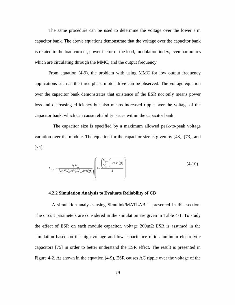
79
The same procedure can be used to determine the voltage over the lower arm
capacitor bank. The above equations demonstrate that the voltage over the capacitor bank
is related to the load current, power factor of the load, modulation index, even harmonics
which are circulating through the MMC, and the output frequency.
From equation (4-9), the problem with using MMC for low output frequency
applications such as the three-phase motor drive can be observed. The voltage equation
over the capacitor bank demonstrates that existence of the ESR not only means power
loss and decreasing efficiency but also means increased ripple over the voltage of the
capacitor bank, which can cause reliability issues within the capacitor bank.
The capacitor size is specified by a maximum allowed peak-to-peak voltage
variation over the module. The equation for the capacitor size is given by [48], [73], and
[74]:
3
2
2
3
4
)(cos.
1)cos(.....3
.
dc
pa
paCC
dc
SM
V
V
VVVN
VPC
(4-10)
4.2.2 Simulation Analysis to Evaluate Reliability of CB
A simulation analysis using Simulink/MATLAB is presented in this section.
The circuit parameters are considered in the simulation are given in Table 4-1. To study
the effect of ESR on each module capacitor, voltage 200mΩ ESR is assumed in the
simulation based on the high voltage and low capacitance ratio aluminum electrolytic
capacitors [75] in order to better understand the ESR effect. The result is presented in
Figure 4-2. As shown in the equation (4-9), ESR causes AC ripple over the voltage of the
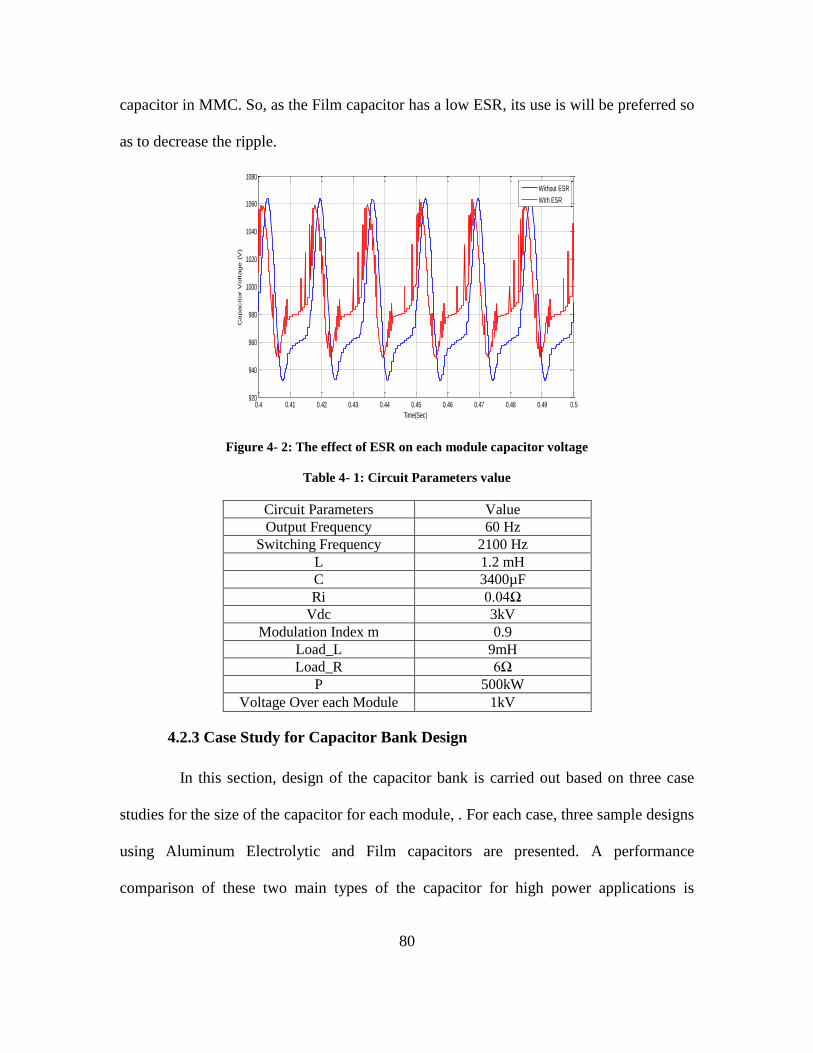
80
capacitor in MMC. So, as the Film capacitor has a low ESR, its use is will be preferred so
as to decrease the ripple.
Figure 4- 2: The effect of ESR on each module capacitor voltage
Table 4- 1: Circuit Parameters value
Circuit Parameters Value
Output Frequency 60 Hz
Switching Frequency 2100 Hz
L 1.2 mH
C 3400µF
Ri 0.04Ω
Vdc 3kV
Modulation Index m 0.9
Load_L 9mH
Load_R 6Ω
P 500kW
Voltage Over each Module 1kV
4.2.3 Case Study for Capacitor Bank Design
In this section, design of the capacitor bank is carried out based on three case
studies for the size of the capacitor for each module, . For each case, three sample designs
using Aluminum Electrolytic and Film capacitors are presented. A performance
comparison of these two main types of the capacitor for high power applications is
0.4 0.41 0.42 0.43 0.44 0.45 0.46 0.47 0.48 0.49 0.5920
940
960
980
1000
1020
1040
1060
1080
Time(Sec)
Capacitor V
oltage (V
)
Without ESR
With ESR

81
presented in [71]. To evaluate the design characteristics of the capacitor bank using
Aluminum Electrolytic and Film capacitors and look into the pros and cons of each, cases
have been chosen to cover instances where the current ripple through the capacitor is
from low to high, respectively.
Table 4- 2: Three Capacitor bank Design Case Studies for different voltage and current ripple
Case C (µF) Voltage Ripple Current Ripple
Case1 3400 Normal Normal
Case2 6000 Low Low
Case3 2500 High High
Each case is shown in Table 4-2. These values in each case follow the equation
(4-10). The current through the capacitor and FFT analysis for the capacitor current in
each of the three cases are shown in Figure 4-3 a, b and c.
4.2.3.1 Aluminum Electrolytic Capacitor
By choosing 1700 µF (500 V) Type 450C 105 °C Ultra-Ripple, Long-life,
Inverter Grade and Radial Leaded [75], the design for case 1 was made using an ALE
capacitor. Because each module’s voltage is 1kV where the reserved voltage factor is
defined as 1.5, and considering the nominal current through the capacitor, it is determined
that three ALE capacitors are needed in series in each parallel branch. Also, because there
is nominal current passing through each capacitor, the capacitor bank needs six parallel
branches.

82
(a) Irms=80.5A (b) Irms=54A (c) Irms=145A
Figure 4- 3: Current waveform through Capacitor and FFT analysis for each three-Case a) Case 1,
b) Case 2 and c) Case 3
4.2.3.2 Film Capacitor
By growing the film capacitors’ technology, they can be made to offer high
operating current, low ESR, and high voltage; however, the capacitance value still is
much lower than it is for Aluminum Electrolytic capacitors. In order to design the
capacitor bank to provide the value specified for case one, two different film capacitors
are selected. First is the 1500 µF, 800 V, Type 947C Polypropylene, Film DC-Link
Capacitor from Cornell Dubilier [76], [77] Secondly, the 1040 µF, 1500 V, E50
Electronicon Film [78] capacitor is considered. The design samples illustrations for case
one using CDE Aluminum, CDE Film, and Electronicon Film capacitor are shown in
Figure 4-4. The design procedure for the other cases is presented following. In cases two
and three, the number of series capacitors are same as in case one. However, in case two
C is equal to 6 mF, and for the ALE capacitor three parellel branches are needed, for
CDE Film eight are needed and for Electronicon Film five parallel branches are needed.
In case three, where C is 2500 µF, for CDE Film four and for Electronicon Film two
parallel branches are required. In case three, the Aluminum Electrolytic Capacitor is
0.3 0.35 0.4 0.45 0.5
-100
0
100
Selected signal: 30 cycles. FFT window (in red): 6 cycles
Time (s)
0 100 200 300 400 5000
10
20
30
40
50
60
70
Frequency (Hz)
Fundamental (60Hz) = 57.28 , THD= 142.72%
Mag
0.3 0.35 0.4 0.45 0.5
-50
0
50
100
Selected signal: 30 cycles. FFT window (in red): 6 cycles
Time (s)
0 50 100 150 200 250 300 350 400 450 5000
10
20
30
40
Frequency (Hz)
Fundamental (60Hz) = 44 , THD= 115.50%
Mag
0.3 0.35 0.4 0.45 0.5
-200
0
200
Selected signal: 30 cycles. FFT window (in red): 6 cycles
Time (s)
0 100 200 300 400 5000
20
40
60
80
100
120
140
Frequency (Hz)
Fundamental (60Hz) = 82.69 , THD= 194.21%
Mag

83
selected from KEMET, 330 µF and 500 V [79], so it needs 36 parallel branch to
overcome the high ripple current.
(a) (b) (c)
Figure 4- 4: Three sample designs illustration for capacitor bank in case 1 C=3400uF (a) CDE ALE
Capacitor Bank Design, (b) CDE Film Capacitor Bank Design, (c) Elecronicon Film Capacitor Bank
Design
4.2.4 Power Loss, Hot Spot, Failure Rate and Reliability Calculations of the
Capacitor Bank
In order to calculate power loss and hot spots in the capacitor bank, it is
assumed that ESR is is constant over frequency. The equations of the power loss and hot
spot temperature based on the true RMS value, ESR, and thermal resistance of the
capacitor bank are shown as follows:
2
rmsLoss IESRP (4-11)
thLossah RPTT (4-12)
Ta is ambient temperature, which is assumed to be 45°C. Generally, the failure
rate of the capacitor can be estimated by using reliability predication model handbooks
such as [80] and [81]. However, based on the applied technology, many manufacturers
provide their own failure rate calculation method for their product. As an example, the
failure rate equation for CDE Aluminum Electrolytic Capacitors is given in [82].
C
C
C
ESR
ESR
ESR
C
C
C
ESR
ESR
ESR
C
C
C
ESR
ESR
ESR
C
C
C
ESR
ESR
ESR
C
C
C
ESR
ESR
ESR
C
C
C
ESR
ESR
ESR
C
C
ESR
ESR
C
C
ESR
ESR
C
C
ESR
ESR
C
C
ESR
ESR
C
C
ESR
ESR
C C C
ESR ESR ESR
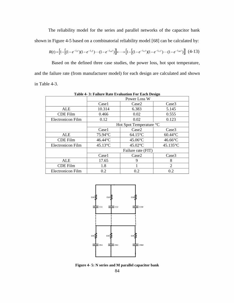
84
The reliability model for the series and parallel networks of the capacitor bank
shown in Figure 4-5 based on a combinatorial reliability model [68] can be calculated by:
)1()1)(1(1)1()1)(1(1)( 2111211 tttttt NMNNM eeeeeetR
(4-13)
Based on the defined three case studies, the power loss, hot spot temperature,
and the failure rate (from manufacturer model) for each design are calculated and shown
in Table 4-3.
Table 4- 3: Failure Rate Evaluation For Each Design
Power Loss W
Case1 Case2 Case3
ALE 10.314 6.383 5.145
CDE Film 0.466 0.02 0.555
Electronicon Film 0.12 0.02 0.123
Hot Spot Temperature °C
Case1 Case2 Case3
ALE 75.94°C 64.15°C 60.44°C
CDE Film 46.44°C 45.06°C 46.66°C
Electronicon Film 45.13°C 45.02°C 45.135°C
Failure rate (FIT)
Case1 Case2 Case3
ALE 17.65 9 8
CDE Film 1.8 1 2
Electronicon Film 0.2 0.2 0.2
C11
ESR
CN1
C12
ESR
CN2
C1M
ESR
CNM
ESR ESR ESR
Figure 4- 5: N series and M parallel capacitor bank

85
4.2.5 Comparison Among Reliability of Each Case
Due to the necessity of calculating the reliability curve of each sample design in
each case, equation (4-13) is used for each design. Then, by replacing calculated failure
rates of each design, which are given in Table III, the reliability function can be achieved.
The reliability curves for each case are shown in Figure 4-6 a, b and c.
As Figure 4-6 shows, in each case, the reliability of the film capacitor bank
designs versus time are higher than that of the ALE capacitor bank.
(a) (b) (c)
Figure 4- 6: Reliability function comparison among three different cases a) Case 1 b) Case 2 and c)
Case 3
4.2.6 Difference Between Reliability of the Internally Parallel Connected and
Non-Connected Capacitor Bank Considering Failure Mode Of the Capacitor
Failure modes and failure mechanisms of the capacitors used in the DC-Link
application are given in [71]. Considering open and short circuit failure modes of the
capacitors, two different approaches for the design of the capacitor bank can be proposed.
The first approach is based on what has been discussed in the previous section, and which
is called the internally parallel connected capacitor bank. This is used when the dominant
failure mode of the capacitor is open circuit. The second approach is just to use no
internally connected parallel caps; this is used for the design when the dominant failure
0 0.5 1 1.5 2 2.5 3 3.5 4 4.5 5
x 109
0
0.1
0.2
0.3
0.4
0.5
0.6
0.7
0.8
0.9
1
Time (h)
R(t
)
3400uF ALE CDE CB
3400uF Film CDE CB
3400uF Film Electronicon CB
0 0.5 1 1.5 2 2.5 3 3.5 4 4.5 5
x 109
0
0.1
0.2
0.3
0.4
0.5
0.6
0.7
0.8
0.9
1
Time (h)
R(t
)
6mF ALE CDE CB
6mF Film CDE CB
6mF Film Electronicon CB
0 0.5 1 1.5 2 2.5 3 3.5 4 4.5 5
x 109
0
0.1
0.2
0.3
0.4
0.5
0.6
0.7
0.8
0.9
1
Time (h)
R(t
)
2500uF ALE CDE CB
2500uF Film CDE CB
2500uF Film Electronicon CB
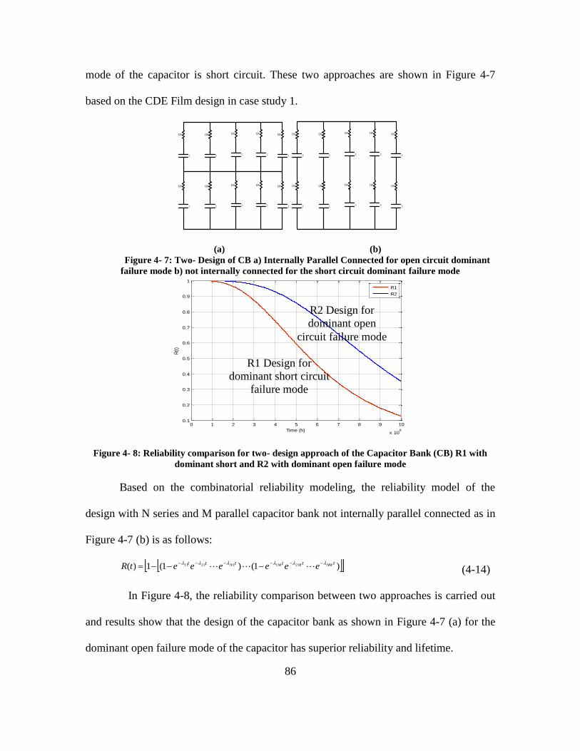
86
mode of the capacitor is short circuit. These two approaches are shown in Figure 4-7
based on the CDE Film design in case study 1.
(a) (b)
Figure 4- 7: Two- Design of CB a) Internally Parallel Connected for open circuit dominant
failure mode b) not internally connected for the short circuit dominant failure mode
Figure 4- 8: Reliability comparison for two- design approach of the Capacitor Bank (CB) R1 with
dominant short and R2 with dominant open failure mode
Based on the combinatorial reliability modeling, the reliability model of the
design with N series and M parallel capacitor bank not internally parallel connected as in
Figure 4-7 (b) is as follows:
(4-14)
In Figure 4-8, the reliability comparison between two approaches is carried out
and results show that the design of the capacitor bank as shown in Figure 4-7 (a) for the
dominant open failure mode of the capacitor has superior reliability and lifetime.
C
C
ESR
ESR
C
C
ESR
ESR
C
C
ESR
ESR
C
C
ESR
ESR
C
C
ESR
ESR
C
C
ESR
ESR
C
C
ESR
ESR
C
C
ESR
ESR
C
C
ESR
ESR
C
C
ESR
ESR
0 1 2 3 4 5 6 7 8 9 10
x 108
0.1
0.2
0.3
0.4
0.5
0.6
0.7
0.8
0.9
1
Time (h)
R(t
)
R1
R2
)1()1(1)( 2112111 tttttt NMMMN eeeeeetR
R2 Design for
dominant open
circuit failure mode
R1 Design for
dominant short circuit
failure mode
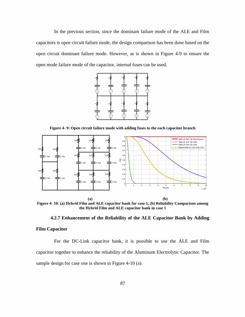
87
In the previous section, since the dominant failure mode of the ALE and Film
capacitors is open circuit failure mode, the design comparison has been done based on the
open circuit dominant failure mode. However, as is shown in Figure 4-9 to ensure the
open mode failure mode of the capacitor, internal fuses can be used.
Figure 4- 9: Open circuit failure mode with adding fuses to the each capacitor branch
C AlE
ESR
C ALE
C ALE
C Film
ESR
C Film
C Film
ESR
C Film
C AlE
ESR
C ALE
C AlE
ESR
C ALE
ESR
ESR
C ALE
ESR
C ALE
ESR
ESR ESR
ESR ESR
(a) (b)
Figure 4- 10: (a) Hybrid Film and ALE capacitor bank for case 1, (b) Reliability Comparison among
the Hybrid Film and ALE capacitor bank in case 1
4.2.7 Enhancement of the Reliability of the ALE Capacitor Bank by Adding
Film Capacitor
For the DC-Link capacitor bank, it is possible to use the ALE and Film
capacitor together to enhance the reliability of the Aluminum Electrolytic Capacitor. The
sample design for case one is shown in Figure 4-10 (a).
C
C
ESR
ESR
C
C
ESR
ESR
C
C
ESR
ESR
C
C
ESR
ESR
C
C
ESR
ESR
0 1 2 3 4 5 6 7 8 9 10
x 108
0
0.1
0.2
0.3
0.4
0.5
0.6
0.7
0.8
0.9
1
Time(h)
R(t
)
3400 uF Film CB Electronicon
3400 uF ALE CB CDE
3400 uF Film CB CDE
Hybrid 3400 uF Film CDE ALE

88
The reliability curve of the hybrid DC-link capacitor is shown in Figure 4-10 (b).
As can be seen in this figure, the reliability of the ALE Capacitor is improved by adding a
film capacitor. Due to unbalanced current sharing between ALE and Film Capacitors, the
ability of the film capacitor to handle higher current than the ALE capacitor means that it
can be used to decrease the power loss and temperature rising and also improve reliability
issues. The proposed structure can be designed for higher energy density than the pure
film capacitor and with higher reliability and longer life than a pure ALE capacitor bank.
4.3 Reliability Modeling of the Capacitor Bank for MMC Using
Markov State-Space Model
One of the drawbacks to the reliability modeling of systems with a high number
of components is that in those systems, a high number of simulations or calculations
should be executed in order to find the system’s characteristics in each state. One solution
to reduce the time and complexity of simulations based on real time models, may be
using the mathematical model of the system. In this study, to estimate the voltage and
current of one cell after the failure of one of the capacitors in the capacitor bank, the
converter mathematical modeling approach is used.
A sub-module of the MMC is modeled as a current source converter in order to
decouple the operation of one module with the operation of the whole converter. Based
on the switching model obtained in Chapter 2, the mathematical equations describing the
dynamic behaviors of the N-modules MMC converter is given by:

89
1
11
2
1
11
1
1
1
2
1( . ) , ,
1( . )
1( . ) 1,...
1( . ) 1,...2
0
0
i
i
i
i
Np u
p i C p a u
i
Nn u
n i C n a u
i N
C
p u i
C
n u i
i upper
i lower
p u
n
diE S V R i V where u a b or c
dt L
diE S V R i V
dt L
dVi S i N
dt C
dVi S i N N
dt C
dC
dt
dC
dt
y i
y i
u
(4-15)
Where ip-u, in-u, iS ,iCV and
a uV are upper/lower arm currents, gating signal of upper
gate, capacitor voltage of i-th cell, and phase-u voltage, respectively. The gating signal of
the lower gate is the complementary ofiS .
Figure 4- 11: The current and voltage through the capacitor bank of one module
The simulation result through the modeling of the MMC with the specifications
set forth above is shown in Figure 4-11. Since the objective is designing the capacitor
0 0.005 0.01 0.015 0.02 0.025 0.03-200
-100
0
100
200
300
400
Time(sec)
Ca
pa
cito
r C
urr
en
t IC
i(A
)
0 0.005 0.01 0.015 0.02 0.025 0.03940
960
980
1000
1020
1040
1060
Time(sec)
Ca
pa
cito
r V
olta
ge
VC
i(V
)
0 0.005 0.01 0.015 0.02 0.025 0.03-200
-100
0
100
200
300
400
Time(sec)
Ca
pa
cito
r C
urr
en
t IC
i(A
)
0 0.005 0.01 0.015 0.02 0.025 0.03940
960
980
1000
1020
1040
1060
Time(sec)
Ca
pa
cito
r V
olta
ge
VC
i(V
)
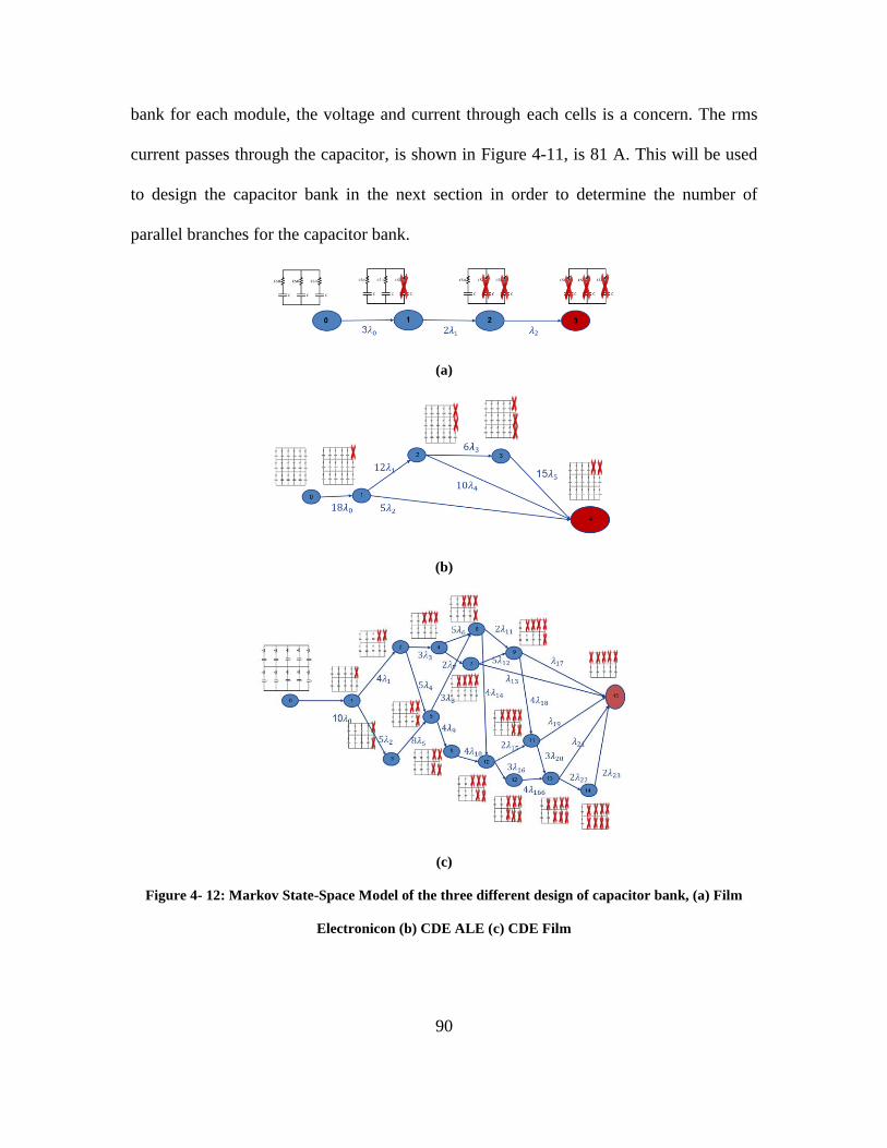
90
bank for each module, the voltage and current through each cells is a concern. The rms
current passes through the capacitor, is shown in Figure 4-11, is 81 A. This will be used
to design the capacitor bank in the next section in order to determine the number of
parallel branches for the capacitor bank.
(a)
(b)
(c)
Figure 4- 12: Markov State-Space Model of the three different design of capacitor bank, (a) Film
Electronicon (b) CDE ALE (c) CDE Film

91
4.3.1 Markov State-Space Model
The Markov model is a graphical representation of the system’s corresponding
states after a unique sequence of component failures and transitions among these states
[68]. The basics of the Markov state-space model can be found in reliability modeling
text books [83] and [84].
The capacitor bank of 3400 µF is designed using three different types of
capacitors. The Aluminum Electrolytic capacitor of 1700 µF (500 V) Type 450C 105 °C
Ultra-Ripple, Long-life, Inverter Grade, and Radial Leaded [75] has been chosen for the
ALE type capacitor bank. For the Film type capacitor bank two different film capacitors
are selected. First, the 1500 µF, 800 V, Type 947C Polypropylene, Film DC-Link
Capacitors from Cornell Dubilier [76], [77] and secondly the 1040 µF, 1500 V, E50
Electronicon Film [78] capacitor are considered. By using the structure of parallel
internally connected capacitors within the capacitor bank, the CDE ALE design leads to
six parallel branches with three series capacitors in each leg. The CDE film design has
five parallel branches with two series individual capacitors and the Electronicon will have
three parallel capacitors. Markov state-space modeling has been done for each of the
three capacitor bank designs. In Figure 4-12, reliability modeling based on the Markov
state space model is shown for each of the three different capacitor banks.
In Figure 4-12, the zero state represents system operation without failure, and the
failure rate to the next system is the failure rate of the component in the corresponding
state. The system failure state called the absorbing state is determined when the current
through the capacitors of the capacitor bank goes higher than the rated current. Knowing
this, it can be deduced that the Film capacitor can last longer after a failure of one
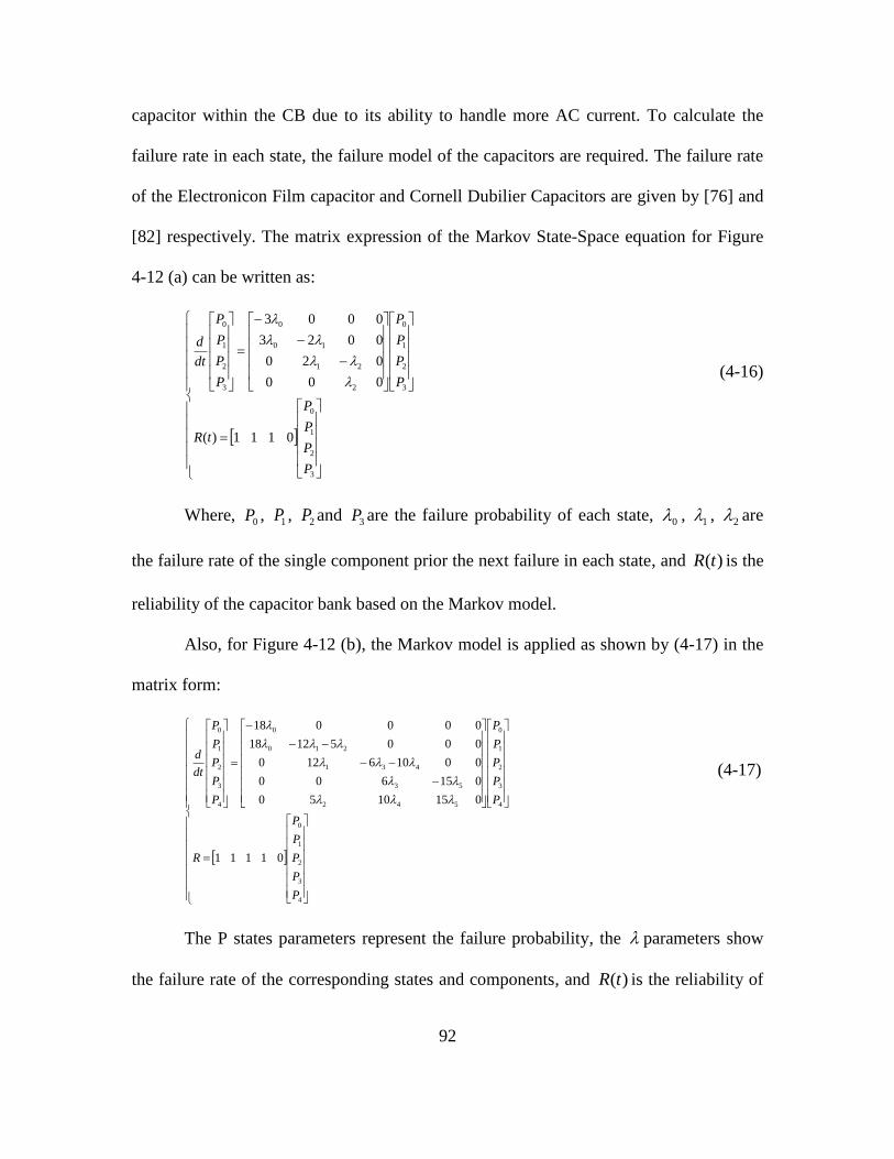
92
capacitor within the CB due to its ability to handle more AC current. To calculate the
failure rate in each state, the failure model of the capacitors are required. The failure rate
of the Electronicon Film capacitor and Cornell Dubilier Capacitors are given by [76] and
[82] respectively. The matrix expression of the Markov State-Space equation for Figure
4-12 (a) can be written as:
3
2
1
0
3
2
1
0
2
21
10
0
3
2
1
0
0111)(
000
020
0023
0003
P
P
P
P
tR
P
P
P
P
P
P
P
P
dt
d
(4-16)
Where, 0P , 1P , 2P and 3P are the failure probability of each state, 0 , 1 , 2 are
the failure rate of the single component prior the next failure in each state, and )(tR is the
reliability of the capacitor bank based on the Markov model.
Also, for Figure 4-12 (b), the Markov model is applied as shown by (4-17) in the
matrix form:
4
3
2
1
0
4
3
2
1
0
542
53
431
210
0
4
3
2
1
0
01111
0151050
015600
00106120
00051218
000018
P
P
P
P
P
R
P
P
P
P
P
P
P
P
P
P
dt
d
(4-17)
The P states parameters represent the failure probability, the parameters show
the failure rate of the corresponding states and components, and )(tR is the reliability of

93
the capacitor bank based on the Markov model. For Figure 4-12 (c), the same procedure
can be used to derive the state-space model. By calculating the failure rate in each state
for each of the three cases, the reliability model of the capacitor bank using the Markov
State-Space Model is achieved.
Figure 4- 13: The Markov reliability model of the capacitor bank which is modeled in Figure 4-12 (a)
Figure 4- 14: The Markov reliability model of the capacitor bank which is modeled in Figure 4-12 (b)
0 0.2 0.4 0.6 0.8 1 1.2 1.4 1.6 1.8 2
x 1010
0
0.1
0.2
0.3
0.4
0.5
0.6
0.7
0.8
0.9
1
Time(h)
Relia
bili
ty
R
P0
P1
P2
P3
0 0.5 1 1.5 2 2.5 3 3.5
x 107
0
0.1
0.2
0.3
0.4
0.5
0.6
0.7
0.8
0.9
1
Time(h)
Relia
bili
ty
R
P0
P1
P2
P3
P4

94
Figure 4- 15: The Markov reliability model of the capacitor bank which is modeled in Figure 4-12 (c)
In Figure 4-13, the reliability model of case a, which is shown in Figure 4-12 (a), is
illustrated. The Markov-reliability model for case b and c in Figure 4-12 is extracted in
the same manner as case a. In Figure 4-14 and 4-15, the reliability model of the
corresponding capacitor bank is depicted. As can be seen in these figures, the reliability
of each state is displayed separately in order to understand the transition that occurs from
the fault free state to the absorbing state.
(a) (b) (c)
Figure 4- 16: The failure rate of the system extracted from Markov Model, (a) Film Electronicon, (b)
ALE CDE and (c) Film CDE
The last state in the reliability model shows the probability of the failure of the entire
system, which can be expressed as the reliability of the system. For calculation of the
0 1 2 3 4 5 6 7 8 9 10
x 108
0
0.1
0.2
0.3
0.4
0.5
0.6
0.7
0.8
0.9
1
Time(h)
Relia
bili
ty
R
P0
P1
P2
P3
P4
P5
P6
P7
P8
P9
P10
P11
P12
P13
P14
P15
0 0.2 0.4 0.6 0.8 1 1.2 1.4 1.6 1.8 2
x 1010
0
0.1
0.2
0.3
0.4
0.5
0.6
0.7
Time(h)
lam
daS
yste
m (
FIT
)
LambdaSys(FIT)
0 0.5 1 1.5 2 2.5 3 3.5
x 107
0
50
100
150
200
250
300
350
400
450
Time(h)
lam
daS
yste
m (
FIT
)
LambdaSys(FIT)
0 0.2 0.4 0.6 0.8 1 1.2 1.4 1.6 1.8 2
x 109
0
10
20
30
40
50
60
70
Time(h)
lam
daS
yste
m (
FIT
)
LambdaSys(FIT)

95
reliability of a system, it is necessary to simulate and analyze the system in each state to
update the failure rate of the system in each state.
(a)
(b)
(c)
Figure 4- 17: The voltage variation over the capacitor bank in each module (a) for Film Electronicon
design Figure 4-12 (a). (b) For ALE CDE design Figure 4-12 (b). and (c) for Film CDE design Figure
4-12 (c)
In the Markov state-space model, the failure rate of the system is modeled as (4-
18):
)(1
)()(
)(
1)(
tP
tP
dt
tdR
tRt
N
Nsys
(4-18)
0 0.005 0.01 0.015 0.02 0.025 0.03-200
-100
0
100
200
300
400
Time(sec)
Capacitor
Curr
ent(
A)
0 0.005 0.01 0.015 0.02 0.025 0.03800
900
1000
1100
1200
Time(sec)
Capacitor
Voltage(V
)
3.12mF
2.08mF
1.04mF
0 0.005 0.01 0.015 0.02 0.025 0.03-200
-100
0
100
200
300
400
Time(sec)
Capacitor
Curr
ent(
A)
0 0.005 0.01 0.015 0.02 0.025 0.03900
950
1000
1050
1100
Time(sec)
Capacitor
Voltage(V
)
3.4mF
3.187mF
3mF
2.914mF
2.833mF
2.756mF
2.615mF
0 0.005 0.01 0.015 0.02 0.025 0.03-200
-100
0
100
200
300
400
Time(sec)
Capacitor
Curr
ent(
A)
0 0.005 0.01 0.015 0.02 0.025 0.03700
800
900
1000
1100
1200
1300
1400
1500
Time(sec)
Ca
pa
cito
r V
olta
ge
(V)
3.75mF
3.33mF
3mF
2.812mF
2.57mF
1.8mF
1.5mF
1mF
0.75mF
0.5mF
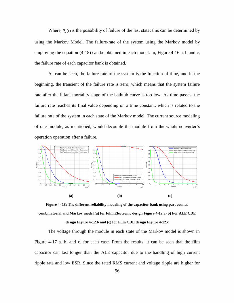
96
Where, )(tPNis the possibility of failure of the last state; this can be determined by
using the Markov Model. The failure-rate of the system using the Markov model by
employing the equation (4-18) can be obtained in each model. In, Figure 4-16 a, b and c,
the failure rate of each capacitor bank is obtained.
As can be seen, the failure rate of the system is the function of time, and in the
beginning, the transient of the failure rate is zero, which means that the system failure
rate after the infant mortality stage of the bathtub curve is too low. As time passes, the
failure rate reaches its final value depending on a time constant. which is related to the
failure rate of the system in each state of the Markov model. The current source modeling
of one module, as mentioned, would decouple the module from the whole converter’s
operation operation after a failure.
(a) (b) (c)
Figure 4- 18: The different reliability modeling of the capacitor bank using part counts,
combinatorial and Markov model (a) for Film Electronic design Figure 4-12.a (b) For ALE CDE
design Figure 4-12.b and (c) for Film CDE design Figure 4-12.c
The voltage through the module in each state of the Markov model is shown in
Figure 4-17 a. b. and c. for each case. From the results, it can be seen that the film
capacitor can last longer than the ALE capacitor due to the handling of high current
ripple rate and low ESR. Since the rated RMS current and voltage ripple are higher for
0 0.2 0.4 0.6 0.8 1 1.2 1.4 1.6 1.8 2
x 1010
0
0.1
0.2
0.3
0.4
0.5
0.6
0.7
0.8
0.9
1
Time(h)
Relia
bili
ty
R(t) Markov Model Film Electronicon
R(t) Combinatorial Model Film Electronicon
R(t) Part Counts Model Film Electronicon
0 0.5 1 1.5 2 2.5 3 3.5
x 107
0
0.1
0.2
0.3
0.4
0.5
0.6
0.7
0.8
0.9
1
Time(h)
Relia
bili
ty
R(t) Markov Model ALE CDE
R(t) Combinatorial Model ALE CDE
R(t) Part Counts Model ALE CDE
0 1 2 3 4 5 6 7 8 9 10
x 108
0
0.1
0.2
0.3
0.4
0.5
0.6
0.7
0.8
0.9
1
Time(h)
Relia
bili
ty
R(t) Markov Model Film CDE
R(t) Combinatorial Model Film CDE
R(t) Part Counts Model Film CDE
97
the film capacitors, in Figure 4-17 a. and c., there are more transient states to the
absorbing state after a failure of one of the capacitors in the capacitor bank. So, using
Film capacitors will mean long life and high reliability in the capacitor bank design in
power electronics systems, especially for the MMC.
4.3.2 Comparison with Three-Reliability Models
This section presents a comprehensive exploration of and comparison among the
results corresponding to the different reliability assessment models of the three reliability
modeling methods mentioned in the previous section, which include the part-count,
combinatorial, and Markov model, In the reliability modeling techniques, the part-count
model provides a simple modeling approach in which the failure of one element causes
the failure of the whole system. This modeling approach gives conservative results in
spite of having simple principles. On the other hand, the combinatorial model leads to
optimistic reliability modeling and allows for the system to work after the failure of its
components. Under this definition, the combinatorial model is used to model the
reliability of redundancy systems. The third modeling method is based on the Markov
state-space model and can model the failure transient of the system as well as the fault
tolerance capability of the system. In Fig. 10.a.b. and c, the comparison among the
different reliability models for each case is shown.
As can be interpreted from the results, modeling of the ALE capacitor bank with
the combinatorial model leads to a very optimistic reliability estimation of the CB, which
realistically hold true. By comparision, the Markov reliability model leads to results that
seems to be closer to the true reliability model of the system in real situations.
98
4.3.3 Conclusion
In this chapter, the reliability of the capacitor bank for Modular Multilevel
Converters (MMC) is modeled using the Markov State-Space Model. The MMC is
modeled mathematically in order to be used for reliability calculations in different states
of the Markov model. Based on a sample case study, the reliability of the capacitor bank
for three different sample designs of the capacitor bank using real capacitors, Film and
Aluminum Electrolytic types, is evaluated using the Markov Model. For each design,
Markov reliability modeling is achieved and based on that, the reliability of each system
is obtained. By using the Markov model, the failure rate of the system for each case is
estimated and finally, a comparison among the results of the reliability modeling of the
system is performed by using the aforementioned three different reliability modeling
techniques (i.e. part-count, combinatorial, and Markov model). The results shows= that
reliability modeling using the Markov model tends to be closeest to the realistic
reliability model of the system.
4.4 Modulation Techniques’ Influence on the Cap Voltage and Arm
Current Ripple
In this section, the modulation technique’s effects on the stress over the sub
module capacitor and the IGBT will be discussed. The evaluation is done based on the
harmonic analysis over the arm quantities. For the phase deposition methods, the carrier
rotation technique [85], [86] and [87] is utilized. To evaluate the effect of adopting each
modulation technique, the case study converter parameters shown in table I are used for
the simulation.

99
Table 4- 4: MMC Parameter values for modulation technique evaluation
Output Frequency 60 Hz
Switching Frequency 540 Hz
L 3.7 mH
C 4000µF
Ri 0.004Ω
Modulation Index m 0.9
Output Voltage 6kV L-L
P 3MW
Voltage Over each
Module 1kV
DC Bus Voltage 10 kV
Number of Module
per arm 10
The Total Harmonic Distortion (THD) of the upper arm current, voltage and
current of the capacitor, output line to line voltage, and current is shown in Table. II.
Table 4- 5: Stress Analysis in Different Modulation Technique
Modulation
Technique IuA THD Vcu THD Voll THD
Io
THD Icap THD
PD 21.97 % 76.22% 6.24 % 2.74 % 193.63%
POD 17.80 % 73.98% 7.73 % 3.57 % 197.56%
APOD 16.71% 70.33% 7.84% 3.36% 188.45%
PSC 13.44% 56.38% 7.22% 0.62 % 187.30%
As shown in the table above, the simulation result shows that the Phase-Shifted
Carrier Modulation method has less harmonic distortion, which is desirable. So, the
Phase-Shifted Carrier modulation technique is chosen for the MMC.

100
4.5 Design of the L and C with Circulating Current Controller
Design of the arm inductor and the size of the sub-module capacitor should be
performed taking into consideration that the circulating current suppressing controller is
utilized. By considering the CCSC effect, the second order harmonic through the upper
arm current would be negligible, and by assuming that the direct modulation scheme is
used, the instantaneous power of the upper arm cells can be written as:
Uasmccc ivivp (4-19)
And by replacing the voltage over the upper arm and the upper arm current, the
instantaneous power of the upper arm can be written as:
)]sin(2
2
3
1)[sin1(
2 tIItM
Vp adc
dcc
(4-20)
By assuming that the peak to peak voltage ripple over the capacitor bank is V2 ,
the maximum energy stored the capacitor will become as follows:
VCVVVCVVCW ddcdc 22
1
2
1 22
max (4-21)
The equation above should be equal to the maximum energy of the upper arm,
which can found by the integral of equation 20. From this equation, the equation for the
size of the capacitor can be found:
32
1 2
cos1
cos32
2
1
M
VNMV
P
VV
dtpC
dd
t
tc (4-22)
By neglecting the second order harmonic current, the voltage across the inductor
becomes as follows [46]:
tI
MtI
M
C
NV dcacir
2cos
62cos2
8
3
2
2
(4-23)
101
The maximum switching frequency circulating current can be written as follows:
s
arm
cirMaxPP T
L
VI .
2_ (4-24)
So, from equation (4-23), the arm inductor size necessary to limit the switching
frequency circulating current can be obtained by [44]:
dcadca
swMaxPP
arm IMIIM
ICfI
NML
2
1
916
9
8
22
2
_ (4-25)
There are three main criteria for the arm inductor, which are as follows: (i)
selection of the arm inductor to limit the DC side fault current [88], (ii) the inductor size
should be selected such that it is prevented from the second order harmonic resonant
frequency [46], (iii) The inductor size should be chosen to limit the circulating current as
it is given in equation (4-25). The size of the inductor would be the maximum of size as
determined from these items.
4.6 Reliability-Oriented Switching Frequency Analysis for the
Modular Multilevel Converter (MMC)
4.6.1 Harmonic Components Analysis of MMC for Low Switching Frequency
Applications
Modular Multilevel Converters are preferably operated at low switching
frequency in order to reduce switching loss of the converter. However, switching
frequency can impact the circulating current magnitude though the arm and can cause the
high distortion of the arm current. The switching frequency circulating current
components of the upper arm can be written as:

102
sp
pSWadcUa tItIIti sinsin2
2)( (4-26)
Where p is the switching frequency component’s angular frequency. Since
triangular phase-shifted carrier modulation is used and each module is Half-Bridge,
according to the double Fourier transformation [89], the switching harmonics would be as
follows:
tMVV
tv dcdca sin
22)(0
(4-27)
tntmnmm
MJm
Vcn
m n
dc cos2
cos2
2
1
nJ is the Bessel function. From the above equation it can be inferred that nm
should be an odd number for the the line frequency of the MMC since it is desirable that
the switching frequency component not have any effect on the output voltage and
current.So, the switching frequency of the components throughout the arm currents
would be as follows:
nkpkpp ...0,,2)12( (4-28)
Using same procedure, the voltage ripple across the capacitor can be calculated as
follows:

103
tC
MIv
tC
MIv
tC
MIv
tC
MIv
tC
MIt
C
Iv
p
p
sw
cu
p
p
sw
cu
p
p
sw
cu
a
cu
dca
cu
p
p
p
sin4
cos2
sin4
2sin16
2
cos2
cos4
2
2
1
(4-29)
And based on equation (3-12), the line frequency and switching frequency voltage
across the arm inductor becomes as follows:
tI
MtI
M
C
NV dcacir
2cos
22cos2
4
3
2
2
(4-30)
tC
MINV
tC
MI
C
INV
tC
MINV
p
p
SWcir
p
p
pSW
p
SWcir
p
p
SWcir
p
p
p
2cos)(16
2
cos)(84
2
2cos)(16
2
22
22
2
22
(4-31)
From equation (4-29) it can be seen that decreasing the switching frequency
causes an increase in the voltage ripple over the capacitor. And in equation (4-31), it can
be shown that decreasing the switching frequency causes an increase of the circulating
voltage and current. The same result can be achieved by analyzing the switching
frequency effect though an inverter LC filter [90].
In Figure 4-19, the switching frequency effect on the voltage and current ripple
of the capacitor and arm inductor of the MMC are shown.
104
(a) (b)
Figure 4- 19: The switching ripple of the arm current and the capacitor voltage with respect to the
frequency
As shown in the above equation, the current ripple over the inductor and the
capacitor will increase at a lower switching frequency. So, choosing the switching
frequency for the MMC will be a trade off between IGBT power loss and maximum
allowable voltage and current ripple through the module capacitor and arm inductor.
Also, the selection of the switching frequency has an impact on the THD of the output
current, which according to IEEE standard 519, should be less than 5% for the weak
power system network [91]. Table 4-6 shows simulation results of the effect of switching
frequency on the THD of the MMC’s output current, the peak to peak voltage ripple of
the capacitor, and the upper arm total harmonic distortion in different frequency ranges.
The choice of switching frequency should be based on the requested specification from
the MMC (i.e. the maximum acceptable voltage ripple over the capacitor is 10%Vdc).
100 200 300 400 500 600 700 800 900 10000
10
20
30
40
50
60
70
80
90
Frequency (Hz)
Max S
W C
ircula
ting C
urr
ent
Rip
ple
(A
)
SW Circulating Current Ripple Isw
100 200 300 400 500 600 700 800 900 100050
100
150
200
250
300
350
400
Frequency (Hz)
Peak t
o P
eak C
apacitor
Voltage R
ipple
(V
)
Peak to Peak Capacitor Voltage Ripple

105
Table 4- 6: Stress Analysis for Different Switching Frequencies
Frequency Io (THD) Vcu (pp-ripple) IuA (THD)
60×5 2.38% 102(V) 39.31%
60×7 0.61% 79 (V) 13.44%
60×9 0.51% 74 (V) 13.4%
As shown, a switching frequency of less than 60×7 Hz can exceed the voltage
ripple within the allowable range. The output frequency also has an effect on the stress
over the capacitor voltage and the upper arm current. Especially at low output frequency,
the stress over the capacitor voltage and the arm current increases drastically [92], [93].
Future work may include an investigation of the stress and finding a way to decrease the
stress at low output frequency, mainly using common mode voltage injection.
4.6.2 Power Loss Calculation of the MMC With and Without Circulating
Current Suppressing Control
In this section, the power loss calculation of the MMC under different operating
frequencies with and without Circulating Current Suppressing Control (CCSC) will be
presented. The circulating current suppressing controller’s effect on converter power loss
is determined as well. Semiconductor losses considered include conduction and switching
losses, and are calculated based on the corresponding datasheets. The specific IGBT and
diode have been selected and details regarding that will be presented later. Specifically,
diode and IGBT conduction losses can be measured using the method presented in [94]
and the devices’ datasheets.
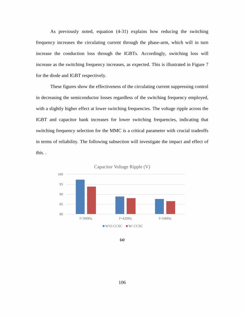
106
As previously noted, equation (4-31) explains how reducing the switching
frequency increases the circulating current through the phase-arm, which will in turn
increase the conduction loss through the IGBTs. Accordingly, switching loss will
increase as the switching frequency increases, as expected. This is illustrated in Figure 7
for the diode and IGBT respectively.
These figures show the effectiveness of the circulating current suppressing control
in decreasing the semiconductor losses regardless of the switching frequency employed,
with a slightly higher effect at lower switching frequencies. The voltage ripple across the
IGBT and capacitor bank increases for lower switching frequencies, indicating that
switching frequency selection for the MMC is a critical parameter with crucial tradeoffs
in terms of reliability. The following subsection will investigate the impact and effect of
this. .
(a)
80
85
90
95
100
f=300Hz f=420Hz f=540Hz
Capacitor Voltage Ripple (V)
W/O CCSC W/ CCSC
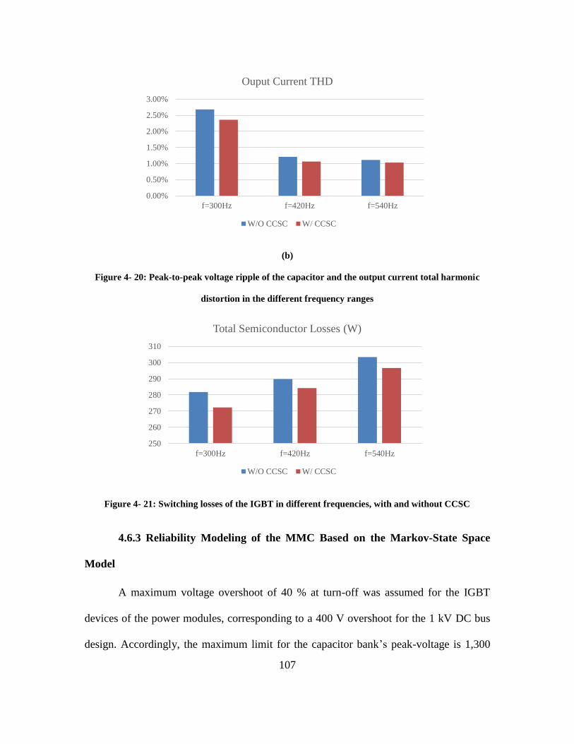
107
(b)
Figure 4- 20: Peak-to-peak voltage ripple of the capacitor and the output current total harmonic
distortion in the different frequency ranges
Figure 4- 21: Switching losses of the IGBT in different frequencies, with and without CCSC
4.6.3 Reliability Modeling of the MMC Based on the Markov-State Space
Model
A maximum voltage overshoot of 40 % at turn-off was assumed for the IGBT
devices of the power modules, corresponding to a 400 V overshoot for the 1 kV DC bus
design. Accordingly, the maximum limit for the capacitor bank’s peak-voltage is 1,300
0.00%
0.50%
1.00%
1.50%
2.00%
2.50%
3.00%
f=300Hz f=420Hz f=540Hz
Ouput Current THD
W/O CCSC W/ CCSC
250
260
270
280
290
300
310
f=300Hz f=420Hz f=540Hz
Total Semiconductor Losses (W)
W/O CCSC W/ CCSC

108
V, at which point the IGBT blocking voltage rating would be surpassed (1,700 V). The
voltage rating chosen for the DC bus film capacitors is consequently 1,300 V, to which a
5 % tolerance is then added by the capacitors’ own specifications. The Markov Chain
model of the conventional power module is shown in Figure 4-22, where State 0 indicates
ten modules operating normally. State 1 indicates that if one capacitor in any power
module fails, the converter can still operate without distorted line current or capacitor
overvoltage. State 2 indicates that if two capacitors in any two power modules fail, the
converter can still keep operating. Any component fault at State 0, 1 and 2 can possibly
lead to a transition to State 3, State 4 or State 5, where the phase-arm is considered failed.
In State 3, a faulty power module is bypassed, requiring a corresponding power module
in the opposite phase-arm to be bypassed in order to maintain the capacitor voltage
balance. This operation does not affect any of the other two converter phase-legs. There
is no remaining fault part in State 3. In State 4, if one capacitor in any of the remaining
nine power modules fails, the converter can still keep working without exceeding its
operational limits and triggering its protection system. In Figure 4-22, the respective
waveforms for States 0 through 4, illustrate, from top to bottom, the phase and line-to-
line AC voltages of the converter, line currents, circulating currents, phase-arm currents,
DC current, and the power module voltages. The progressive deterioration of the
distortion of these waveforms, aside from the AC variables, shows how the converter can
still operate as long as its internal voltage and current limits are not exceeded.

109
(a) State 0 (b) State 1 (c) State 2
(d) State 3 (e) State 4
Figure 4- 22: Reliability Model of the Modular Multilevel Converter with three-phase output voltage,
current, circulating current, upper arm, DC current and capacitor voltage in each failure state
1.6 1.61 1.62 1.63 1.64 1.65 1.66
-1
-0.5
0
0.5
1
x 104
vam
vbm
vc m
vab
1.6 1.61 1.62 1.63 1.64 1.65 1.66-500
0
500
ipha
iphb
iphc
1.6 1.61 1.62 1.63 1.64 1.65 1.66
-500
0
500
icira
icirb
icirc
1.6 1.61 1.62 1.63 1.64 1.65 1.66
-500
0
500
iUa
iUb
iUc
idc
1.6 1.61 1.62 1.63 1.64 1.65 1.66
800
1000
1200
vCUa1
vCL a1
1.6 1.61 1.62 1.63 1.64 1.65 1.66
-1
-0.5
0
0.5
1
x 104
vam
vbm
vc m
vab
1.6 1.61 1.62 1.63 1.64 1.65 1.66-500
0
500
ipha
iphb
iphc
1.6 1.61 1.62 1.63 1.64 1.65 1.66
-500
0
500
icira
icirb
icirc
1.6 1.61 1.62 1.63 1.64 1.65 1.66
-500
0
500
iUa
iUb
iUc
idc
1.6 1.61 1.62 1.63 1.64 1.65 1.66
800
1000
1200
vCUa1
vCUa2
vCUa3
vCL a1
1.6 1.61 1.62 1.63 1.64 1.65 1.66
-1
-0.5
0
0.5
1
x 104
vam
vbm
vc m
vab
1.6 1.61 1.62 1.63 1.64 1.65 1.66-500
0
500
ipha
iphb
iphc
1.6 1.61 1.62 1.63 1.64 1.65 1.66
-500
0
500
icira
icirb
icirc
1.6 1.61 1.62 1.63 1.64 1.65 1.66
-500
0
500
iUa
iUb
iUc
idc
1.6 1.61 1.62 1.63 1.64 1.65 1.66
800
1000
1200
vCUa2
vCL a2
vCL b2
vCL b2
1.6 1.61 1.62 1.63 1.64 1.65 1.66
-1
-0.5
0
0.5
1
x 104
vam
vbm
vc m
vab
1.6 1.61 1.62 1.63 1.64 1.65 1.66-500
0
500
ipha
iphb
iphc
1.6 1.61 1.62 1.63 1.64 1.65 1.66
-500
0
500
icira
icirb
icirc
1.6 1.61 1.62 1.63 1.64 1.65 1.66
-500
0
500
iUa
iUb
iUc
idc
1.6 1.61 1.62 1.63 1.64 1.65 1.66
800
1000
1200
vCUa2
vCUa3
vCL a2
vCL b2
vCL b2

110
Figure 4- 23: Markov Reliability Model of the MMC with Circulating Current Suppressing
Controller in different frequencies
4.6.4 Reliability Comparison of MMC Under Different Frequencies With and
Without Circulating Current Controller
The full Markov reliability model of the MMC and the corresponding analysis
results were presented in the previous section. What follows focuses on the non-
redundant reliability model of the MMC, investigating reliability tradeoffs under different
switching frequencies with and without CCSC. Figure 4-23 shows a plot of the
probability for failure in time for the MMC operating at a switching frequency of 300 Hz,
420 Hz, and 540 Hz, with and without CCSC, where it can be concluded that the
circulating current controller does have a positive impact on the converter’s reliability.
As a final comparison, the reliability models obtained for each switching frequency with
CCSC are depicted in Fig. 9 for comparison purposes. As shown, the 420 Hz case
achieved the best reliability performance, although only a minor overall impact was
determined. This result shows that although fewer semiconductor losses are incurred
111
when operating at lower switching frequencies, the increase of the voltage ripple across
capacitors and IGBTs can detrimentally affect the reliability of the converter, illustrating
one of the key tradeoffs when designing the MMC.
4.6.5 Conclusions
This section presents a reliability oriented switching frequency analysis for the
MMC in different applications. The stress analysis of the MMC for phase-arm currents
and voltages, as well as the converters’ output voltage and current, is conducted by
evaluating the impact of switching frequencies’ harmonic components in the low
switching rate. The effect of a circulating current suppressing controller is also
investigated. The switching frequency evaluation showed an optimum point favoring a
medium switching rate, as the circulating current harmonic content was seen to increase
at lower frequencies, resulting in heightened conduction losses for the devices and a
higher voltage ripple for the power-cell capacitors.
4.7 AAC Design Considerations
4.7.1 Number of Cells in the AAC
One of the promising features of the AAC is that to provide the same voltage
level as the MMC, the AAC needs only about half the number of power cells,
comparatively. The voltage over each module is almost half the rated voltage of modules
in the MMC. To calculate the voltage over the stack, if assuming that the voltage over the
arm inductor is negligible and that the AAC works in the sweet spot, the voltage of the
upper stack can be written as:
112
)27.1(2
)27.01(2
)1(2
2
min
maxDCDC
stack
DCstack
DCstack VV
V
MV
V
VV
(4-32)
The above voltage range compared to the stack voltage in the MMC is almost
half, as shown in (4-33):
DC
DC
stack
stack
DCDC
stack VV
V
V
VVV
)11(
20
22
min
max (4-33)
So, the AAC with a full-bridge module has almost the same number of cells as the
MMC half-bridge when the voltage level is assigned.
By having the rated voltage of each cell for the AAC, the number of cells can be
defined as:
Cell
DCcellAAC
V
VN
2 (4-34)
In contrast, the number of cells for the MMC can be written as:
Cell
DCcellMMC
V
VN (4-35)
4.7.2 Number of Director Switches in the AAC
The number of director switches can be calculated based on the maximum voltage
over the DS, which is the difference between the output voltage and the voltages of the
same arm stacks when DS is off. In Figure 4-24, the voltage over each DS can be seen in
the average mode. So for the upper and lower arm, voltage over DS switches can be
obtained by:
stackDC
acDS vV
vV 2
(4-36)
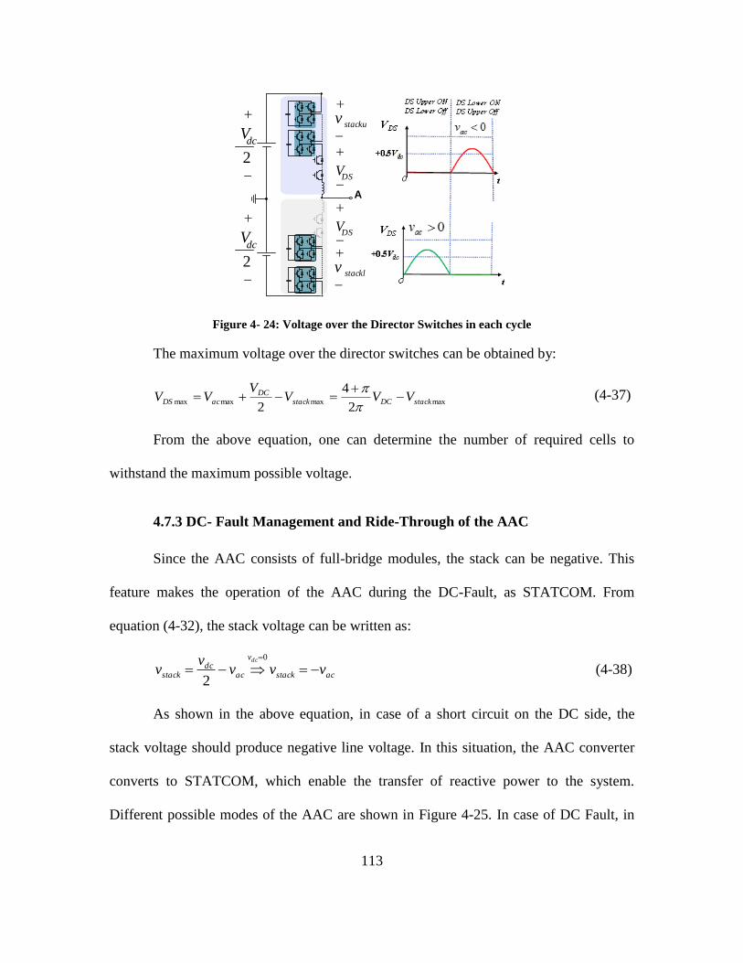
113
A
stackuv
DS
V
DS
V
stacklv
dc
2
V
dc
2
V
Figure 4- 24: Voltage over the Director Switches in each cycle
The maximum voltage over the director switches can be obtained by:
maxmaxmaxmax2
4
2stackDCstack
DC
acDS VVVV
VV
(4-37)
From the above equation, one can determine the number of required cells to
withstand the maximum possible voltage.
4.7.3 DC- Fault Management and Ride-Through of the AAC
Since the AAC consists of full-bridge modules, the stack can be negative. This
feature makes the operation of the AAC during the DC-Fault, as STATCOM. From
equation (4-32), the stack voltage can be written as:
acstack
v
acdc
stack vvvv
vdc
0
2 (4-38)
As shown in the above equation, in case of a short circuit on the DC side, the
stack voltage should produce negative line voltage. In this situation, the AAC converter
converts to STATCOM, which enable the transfer of reactive power to the system.
Different possible modes of the AAC are shown in Figure 4-25. In case of DC Fault, in
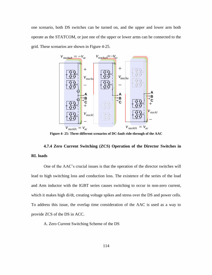
114
one scenario, both DS switches can be turned on, and the upper and lower arm both
operate as the STATCOM, or just one of the upper or lower arms can be connected to the
grid. These scenarios are shown in Figure 4-25.
ABC
ABC
ABC
acstackuA vv
stackuv
stacklv
acstacklA vv
stackuv
acstackuA vv
stacklv
acstacklA vv
Figure 4- 25: Three different scenarios of DC-fault ride-through of the AAC
4.7.4 Zero Current Switching (ZCS) Operation of the Director Switches in
RL loads
One of the AAC’s crucial issues is that the operation of the director switches will
lead to high switching loss and conduction loss. The existence of the series of the load
and Arm inductor with the IGBT series causes switching to occur in non-zero current,
which it makes high di/dt, creating voltage spikes and stress over the DS and power cells.
To address this issue, the overlap time consideration of the AAC is used as a way to
provide ZCS of the DS in ACC.
A. Zero Current Switching Scheme of the DS
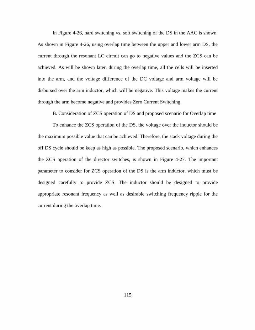
115
In Figure 4-26, hard switching vs. soft switching of the DS in the AAC is shown.
As shown in Figure 4-26, using overlap time between the upper and lower arm DS, the
current through the resonant LC circuit can go to negative values and the ZCS can be
achieved. As will be shown later, during the overlap time, all the cells will be inserted
into the arm, and the voltage difference of the DC voltage and arm voltage will be
disbursed over the arm inductor, which will be negative. This voltage makes the current
through the arm become negative and provides Zero Current Switching.
B. Consideration of ZCS operation of DS and proposed scenario for Overlap time
To enhance the ZCS operation of the DS, the voltage over the inductor should be
the maximum possible value that can be achieved. Therefore, the stack voltage during the
off DS cycle should be keep as high as possible. The proposed scenario, which enhances
the ZCS operation of the director switches, is shown in Figure 4-27. The important
parameter to consider for ZCS operation of the DS is the arm inductor, which must be
designed carefully to provide ZCS. The inductor should be designed to provide
appropriate resonant frequency as well as desirable switching frequency ripple for the
current during the overlap time.
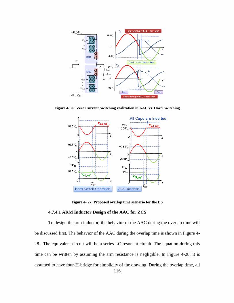
116
A
m
+0.5Vdc
-0.5Vdc
+
VCell
-+
VCell
-
+
VCell
-
+
VCell
-
LLoad
RLoad
DS2
DS1
Figure 4- 26: Zero Current Switching realization in AAC vs. Hard Switching
Figure 4- 27: Proposed overlap time scenario for the DS
4.7.4.1 ARM Inductor Design of the AAC for ZCS
To design the arm inductor, the behavior of the AAC during the overlap time will
be discussed first. The behavior of the AAC during the overlap time is shown in Figure 4-
28. The equivalent circuit will be a series LC resonant circuit. The equation during this
time can be written by assuming the arm resistance is negligible. In Figure 4-28, it is
assumed to have four-H-bridge for simplicity of the drawing. During the overlap time, all

117
capacitors are connected positively to the arm, so that the equivalent circuit will be
simply L and C circuit. Notice that during overlap the output voltage is close to zero. So,
the upper and lower arm can be separate from the two resonant LC series converter. The
equivalent circuit is shown in Figure 4-29. By assuming that the current in this mode is
i(t) and the direction of that is in a negative direction of the load current, the current
equation can be written as:
AB
C
m
+0.5Vdc
-0.5Vdc
+
VCell
-+
VCell
-
+
VCell
-
+
VCell
-
A
m
+0.5Vdc
-0.5Vdc
+
VCell
-
C
C
C
C
L
L
C
C
C
C
+
VCell
-+
VCell
-+
VCell
-
+
VCell
-+
VCell
-+
VCell
-+
VCell
-
+
VL
-
LIDuring OV
0)( ti
Figure 4- 28: The behavior of the AAC during the overlap time
Ve
Le
0)( ti
LI
Ce
Figure 4- 29: The equivalent circuit of the AAC during overlap
e
en
ee
r
r
n
erL
C
LZ
CL
tZ
VtIti
,1
sincos)(
(4-39)
Where, Ve is the equivalent voltage over the inductor as:
118
2
DCCelle
VNVV (4-40)
Notice that during overlap time we have DCcell VNV 2 . So the negative voltage
will be across the inductor.
To provide ZCS, the i(t), the current of the equivalent circuit, should make the
initial negative load current positive. So, in order to provide ZCS, the current should be
positive, as:
0)( ovti (4-41)
From condition (4-41) and equation (4-39), the condition for the inductor will be
obtained as follows:
e
novr
V
IZt
sintan max (4-42)
One of the simple ways to find the value of the maximum inductor is by noticing
that for ovrt , the current will be positive, so the maximum inductor will be as
follows:
21
ov
e
e
t
CL (4-43)
Where, tov is the overlap time between the upper and lower DS. Since during the
overlap time the load inductor load has nothing to do with the inner loop, the value of the
inductor cannot be set to low because of the switching frequency ripple. To ensure
appropriate current frequency ripple, the inductor selection should meet minimum
requirements. The voltage over the arm inductor can be written as:
119
dt
dILVL 2max (4-44)
max
maxmax
max
22
2
II
FL
VIFILV
VNVV
s
LsL
DCcellL
(4-45)
Where Fs is the equivalent frequency of the converter considering interleaving.
From (4-45), the condition for the arm inductor to provide the required switching
frequency ripple is obtained as:
s
L
FI
VL
max
max
2 (4-46)
From (4-43) and (4-46), the required size of the arm inductor will be determined.
Since, in the AAC, there is no circulating current between the upper and lower arm, the
size of the inductor will be expected to be relatively low in comparision to the arm
inductor for the MMC.
4.7.4.2 Power Cell Capacitor Bank Design
The capacitor bank design for each module is taken from Reference [62]. The
required capacitor bank size can be obtained by following the equation. The procedure
used to find the capacitor size is same as for that of the MMC. Results show that the
required capacitor size for the AAC is almost half of the capacitor size of each module in
the MMC. The capacitor sizes of the AAC and the MMC are shown in (4-47):
VVN
EC
cellNcell
stackcell
2 (4-47)
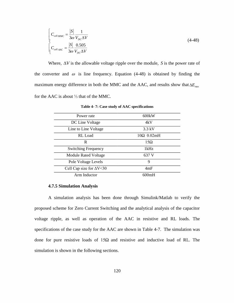
120
VV
SC
VV
SC
DC
AACcell
DC
MMCcell
505.0
3
1
3
(4-48)
Where, V is the allowable voltage ripple over the module, S is the power rate of
the converter and is line frequency. Equation (4-48) is obtained by finding the
maximum energy difference in both the MMC and the AAC, and results show thatmaxE
for the AAC is about ⅓ that of the MMC.
Table 4- 7: Case study of AAC specifications
Power rate 600kW
DC Line Voltage 4kV
Line to Line Voltage 3.3 kV
RL Load 10Ω 0.02mH
R 15Ω
Switching Frequency 1kHz
Module Rated Voltage 637 V
Pole Voltage Levels 9
Cell Cap size for ΔV<30 4mF
Arm Inductor 600mH
4.7.5 Simulation Analysis
A simulation analysis has been done through Simulink/Matlab to verify the
proposed scheme for Zero Current Switching and the analytical analysis of the capacitor
voltage ripple, as well as operation of the AAC in resistive and RL loads. The
specifications of the case study for the AAC are shown in Table 4-7. The simulation was
done for pure resistive loads of 15Ω and resistive and inductive load of RL. The
simulation is shown in the following sections.
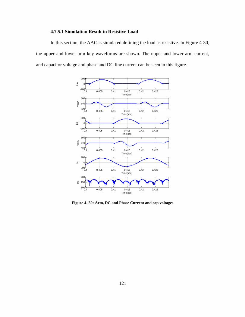
121
4.7.5.1 Simulation Result in Resistive Load
In this section, the AAC is simulated defining the load as resistive. In Figure 4-30,
the upper and lower arm key waveforms are shown. The upper and lower arm current,
and capacitor voltage and phase and DC line current can be seen in this figure.
Figure 4- 30: Arm, DC and Phase Current and cap voltages
0.4 0.405 0.41 0.415 0.42 0.425-200
0
200
Time(sec)
IuA
0.4 0.405 0.41 0.415 0.42 0.425620
640
660
Time(sec)
VcuA
0.4 0.405 0.41 0.415 0.42 0.425-200
0
200
Time(sec)
IlA
0.4 0.405 0.41 0.415 0.42 0.425620
640
660
Time(sec)
VclA
0.4 0.405 0.41 0.415 0.42 0.425-200
0
200
Time(sec)
Ia
0.4 0.405 0.41 0.415 0.42 0.425100
150
200
Time(sec)
Idc
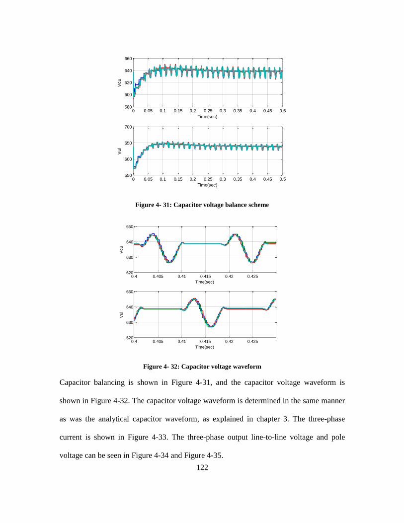
122
Figure 4- 31: Capacitor voltage balance scheme
Figure 4- 32: Capacitor voltage waveform
Capacitor balancing is shown in Figure 4-31, and the capacitor voltage waveform is
shown in Figure 4-32. The capacitor voltage waveform is determined in the same manner
as was the analytical capacitor waveform, as explained in chapter 3. The three-phase
current is shown in Figure 4-33. The three-phase output line-to-line voltage and pole
voltage can be seen in Figure 4-34 and Figure 4-35.
0 0.05 0.1 0.15 0.2 0.25 0.3 0.35 0.4 0.45 0.5580
600
620
640
660
Time(sec)V
cu
0 0.05 0.1 0.15 0.2 0.25 0.3 0.35 0.4 0.45 0.5550
600
650
700
Time(sec)
Vul
0.4 0.405 0.41 0.415 0.42 0.425620
630
640
650
Time(sec)
Vcu
0.4 0.405 0.41 0.415 0.42 0.425620
630
640
650
Time(sec)
Vul
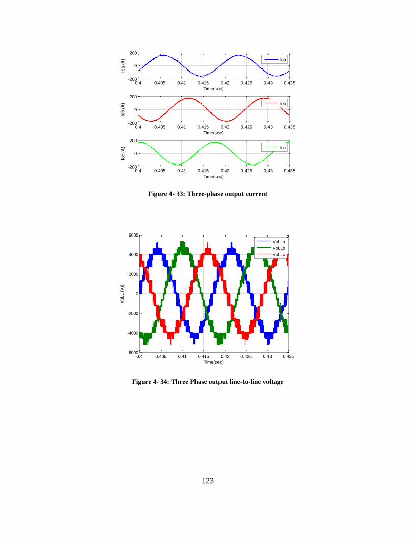
123
Figure 4- 33: Three-phase output current
Figure 4- 34: Three Phase output line-to-line voltage
0.4 0.405 0.41 0.415 0.42 0.425 0.43 0.435-200
0
200
Time(sec)
Ioa (
A)
Ioa
0.4 0.405 0.41 0.415 0.42 0.425 0.43 0.435-200
0
200
Time(sec)
Iob (
A)
Iob
0.4 0.405 0.41 0.415 0.42 0.425 0.43 0.435-200
0
200
Time(sec)
Ioc (
A)
Ioc
0.4 0.405 0.41 0.415 0.42 0.425 0.43 0.435-6000
-4000
-2000
0
2000
4000
6000
Time(sec)
VoLL (
V))
VoLLa
VoLLb
VoLLc

124
Figure 4- 35: Three Phase output pole voltages
Figure 4- 36: Upper Arm DS voltage and current
As shown, the output three-phase pole voltage has 9 levels and the line-to-line
voltage has 19 levels when the number of cells are 4 full-bridge. The upper arm DS
voltage and current are shown in Figure 4-36.
0.4 0.405 0.41 0.415 0.42 0.425 0.43 0.435-3000
-2000
-1000
0
1000
2000
3000
Time(sec)
Vop (
V))
Vopa
Vopb
Vopc
0.435 0.44 0.445 0.45 0.455-500
0
500
1000
1500
2000
2500
3000
Time(sec)
Voltage a
nd C
urr
ent
DS
uA
Upper Arm DS Voltage
Upper Arm DS Cuurent
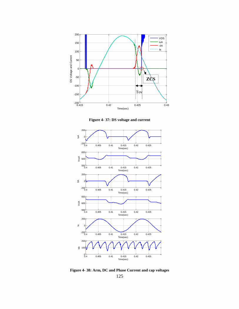
125
Figure 4- 37: DS voltage and current
Figure 4- 38: Arm, DC and Phase Current and cap voltages
0.415 0.42 0.425 0.43-200
-150
-100
-50
0
50
100
150
200
Time(sec)
DS
Voltage a
nd C
urr
ent
VDS
iuA
-ilA
Ia
0.4 0.405 0.41 0.415 0.42 0.425-200
0
200
Time(sec)
IuA
0.4 0.405 0.41 0.415 0.42 0.425550
600
650
Time(sec)
VcuA
0.4 0.405 0.41 0.415 0.42 0.425-200
0
200
Time(sec)
IlA
0.4 0.405 0.41 0.415 0.42 0.425550
600
650
Time(sec)
VclA
0.4 0.405 0.41 0.415 0.42 0.425-200
0
200
Time(sec)
Ia
0.4 0.405 0.41 0.415 0.42 0.4250
100
200
Time(sec)
Idc
ZCS
Tov
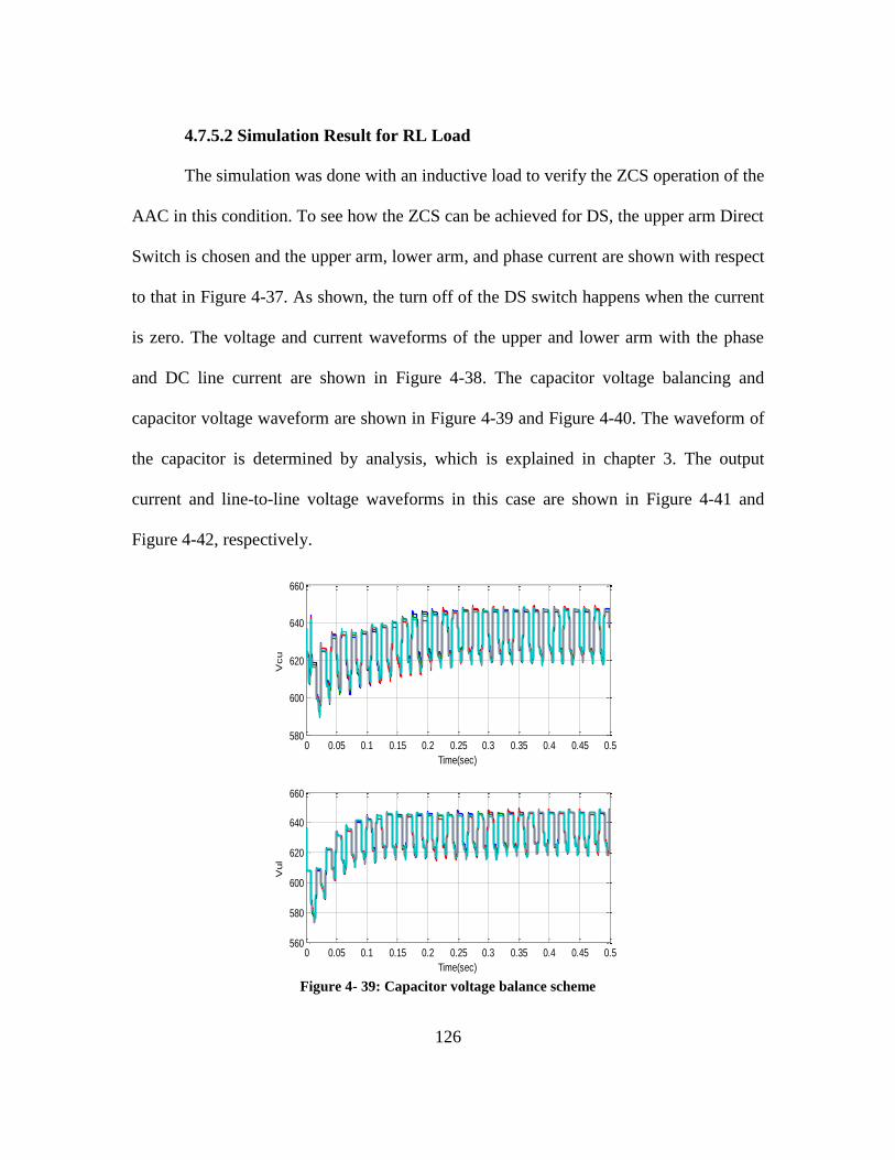
126
4.7.5.2 Simulation Result for RL Load
The simulation was done with an inductive load to verify the ZCS operation of the
AAC in this condition. To see how the ZCS can be achieved for DS, the upper arm Direct
Switch is chosen and the upper arm, lower arm, and phase current are shown with respect
to that in Figure 4-37. As shown, the turn off of the DS switch happens when the current
is zero. The voltage and current waveforms of the upper and lower arm with the phase
and DC line current are shown in Figure 4-38. The capacitor voltage balancing and
capacitor voltage waveform are shown in Figure 4-39 and Figure 4-40. The waveform of
the capacitor is determined by analysis, which is explained in chapter 3. The output
current and line-to-line voltage waveforms in this case are shown in Figure 4-41 and
Figure 4-42, respectively.
Figure 4- 39: Capacitor voltage balance scheme
0 0.05 0.1 0.15 0.2 0.25 0.3 0.35 0.4 0.45 0.5580
600
620
640
660
Time(sec)
Vcu
0 0.05 0.1 0.15 0.2 0.25 0.3 0.35 0.4 0.45 0.5560
580
600
620
640
660
Time(sec)
Vul

127
Figure 4- 40: Capacitor voltage waveform
Figure 4- 41: Three Phase output line to line voltage
Figure 4- 42: Three-phase output current
0.4 0.405 0.41 0.415 0.42 0.425590
600
610
620
630
Time(sec)
Vcu
0.4 0.405 0.41 0.415 0.42 0.425600
610
620
630
640
Time(sec)
Vul
0.4 0.405 0.41 0.415 0.42 0.425 0.43 0.435-200
-150
-100
-50
0
50
100
150
200
Time(sec)
Outp
ut
Curr
ent
Ioa
Iob
Ioc
0.4 0.405 0.41 0.415 0.42 0.425 0.43 0.435-6000
-4000
-2000
0
2000
4000
6000
Time(sec)
Lin
e t
o L
ine V
oltage
Vlla
Vllb
Vllc

128
4.8 Design and Switching Losses Comparison Between AAC and MMC
In this section, the design comparison between the AAC and Half Bridge MMC
will be discussed. The specification is shown in Table 4-7 for both AAC and MMC. The
design procedure is shown in the following.
To achieve the required pole voltage level, the number of half-bridge cells can be
obtained for both the MMC and AAC as given in:
6372
4912
cell
DCCellAAC
cellAACcellAAC
N
VV
NNLevel
(4-49)
And for MMC, we have:
637,27.1
891
_
_
cell
NEWDC
CellMMCDCNEWDC
cellMMCcellMMC
N
VVVV
NNLevel
(4-50)
Notice that since the MMC cannot work in over-modulation mode to produce the
same voltage rate at the output, we assume that the DC voltage will be boosted to 1.27×V
DC to provide same voltage range. From equation (4-37), the voltage over the director
switches can be obtained. A reliability-oriented selection method for IGBT has been done
in [95]. By using the IGBT module FZ800R12KE3, 1.2kV, and 800 A rated current, the
design of the module and DS for both the MMC and AAC has been carried out. In Table
4-8, the number of IGBT switches, capacitor size, and required arm inductor are given for
the MMC and AAC.

129
Table 4- 8: Number of switches in AAC and MMC
Number of SW AAC MMC (Half-Bridge)
Module 32 32
DS 12 0
ARM Inductor 0.6mH 3mH
Module Cap Size
ΔV<30 4mF 8mF
The AAC and MMC (half-bridge) switching losses are shown in Figure 4-43 and
Figure 4-44. The conduction losses and switching losses are estimated based on [94]. As
shown, the switching losses and conduction losses in MMC are a little higher because of
the relatively high circulating current in the MMC. The director switches also have high
conduction and switching losses, which is not desirable. The total switching losses of the
AAC vs. the MMC (half- bridge) is shown in Figure 4-45.
Figure 4- 43: AAC switching power losses
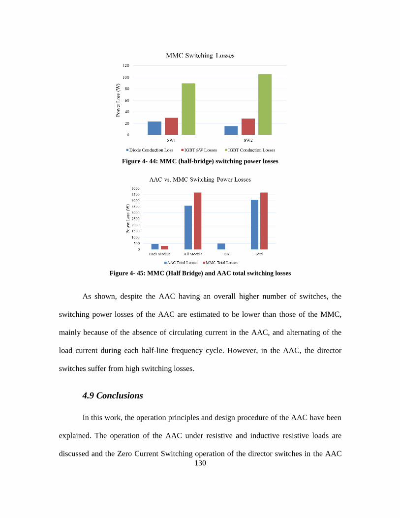
130
Figure 4- 44: MMC (half-bridge) switching power losses
Figure 4- 45: MMC (Half Bridge) and AAC total switching losses
As shown, despite the AAC having an overall higher number of switches, the
switching power losses of the AAC are estimated to be lower than those of the MMC,
mainly because of the absence of circulating current in the AAC, and alternating of the
load current during each half-line frequency cycle. However, in the AAC, the director
switches suffer from high switching losses.
4.9 Conclusions
In this work, the operation principles and design procedure of the AAC have been
explained. The operation of the AAC under resistive and inductive resistive loads are
discussed and the Zero Current Switching operation of the director switches in the AAC
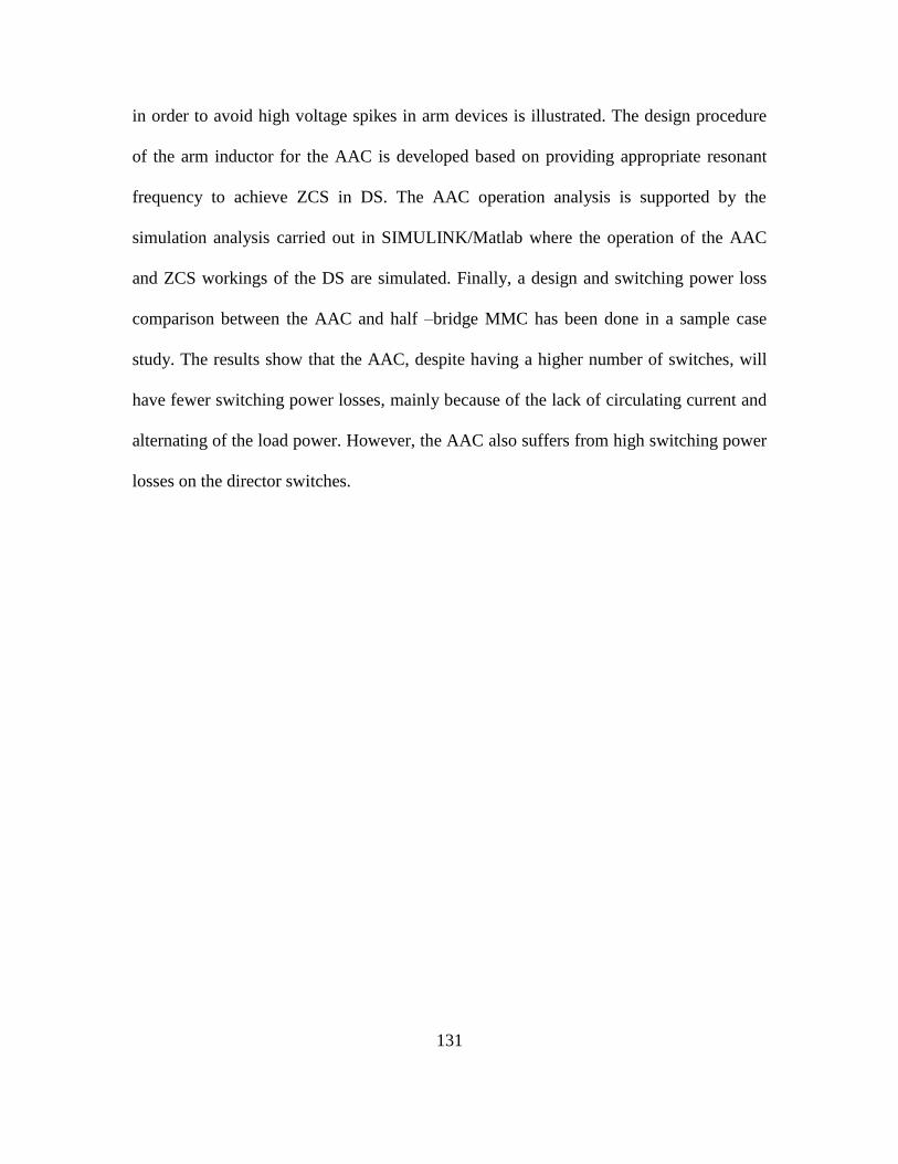
131
in order to avoid high voltage spikes in arm devices is illustrated. The design procedure
of the arm inductor for the AAC is developed based on providing appropriate resonant
frequency to achieve ZCS in DS. The AAC operation analysis is supported by the
simulation analysis carried out in SIMULINK/Matlab where the operation of the AAC
and ZCS workings of the DS are simulated. Finally, a design and switching power loss
comparison between the AAC and half –bridge MMC has been done in a sample case
study. The results show that the AAC, despite having a higher number of switches, will
have fewer switching power losses, mainly because of the lack of circulating current and
alternating of the load power. However, the AAC also suffers from high switching power
losses on the director switches.

132
Chapter 5 DC Fault Ride-Through Capability of
Modular Multilevel Converters
5.1 Motivation
One of the main issues of Modular Multilevel Converters with half-bridge power
cells is their lack of DC-fault blocking capability. To tackle this issue, a full-bridge power
cells-based structure should be employed to rid the MMC of an uncontrollable current
path in case of a collapse of the DC bus voltage. Either the MMC structure with full-
bridge building blocks or the recently developed AAC can be used to solve this problem.
In this chapter, the fault ride-through capability of the MMC with full-bridge power cells
and the AAC during a local terminal to terminal short circuit of the DC-link for medium
voltage DC applications is illustrated. The employed control scheme provides blocking of
the fault current as well as capacitor voltage control during the DC fault. The simulation
analysis is carried out using SIMULINK/ MATLAB for both the MMC with full-bridge
power cells and the AAC during both normal operation and DC fault interrupt in order to
illustrate the operation of the adopted fault control scheme. Finally, an overall
comparison is presented for the MMC with full-bridge cells and the AAC in terms of the
DC fault blocking capability and other related aspects.
133
5.2 Introduction
One of the main issues of the conventional MMC structure with half-bridge power
cells is their inability to block current during DC side faults. Basically, the conventional
MMC suffers from poor DC fault performance that requires fast circuit breakers to
disconnect the converter by opening from the AC side [96],[97]. In addition, time delay
associated with the opening of the circuit breaker on the AC side imposes high fault
currents through the uncontrolled path of the antiparallel diode in the half bridge MMC
[88]. The other solution for tripping the DC fault current in the VSC converter for high
and medium voltage applications is interrupting the DC fault by using DC circuit
breakers [98]. However, the technology is neither mature nor cost effective and will add
more complexity since the DC circuit breakers have to provide the following
functionality: (i) Make a current zero crossing to interrupt the current, (ii) dissipate the
energy stored in the system inductance and (iii) withstand the voltage response of the
network after current interruption [99]. In Figure 5-1 (a) the conventional MMC with
half-bridge modules is shown during the DC fault. The modular multilevel converters
(MMC) include two arms per phase, where in each arm several identical sub-modules are
connected in series. To limit inrush currents and other current transients (circulating
currents) that occur due to the intrinsic switching-action voltage difference between the
converter phase-legs during normal operation [100], two arm inductors will be added in
series with other cells. Each cell in the modular multilevel converter can be realized as a
half-bridge or full-bridge circuit or it can be a series connections of switches in the so-
called hybrid topologies of the modular multilevel converters [23], [29],[36]. As
previously mentioned, the half-bridge topology of the MMC suffers from the
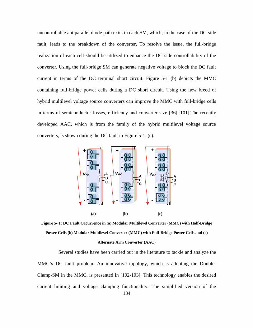
134
uncontrollable antiparallel diode path exits in each SM, which, in the case of the DC-side
fault, leads to the breakdown of the converter. To resolve the issue, the full-bridge
realization of each cell should be utilized to enhance the DC side controllability of the
converter. Using the full-bridge SM can generate negative voltage to block the DC fault
current in terms of the DC terminal short circuit. Figure 5-1 (b) depicts the MMC
containing full-bridge power cells during a DC short circuit. Using the new breed of
hybrid multilevel voltage source converters can improve the MMC with full-bridge cells
in terms of semiconductor losses, efficiency and converter size [36],[101].The recently
developed AAC, which is from the family of the hybrid multilevel voltage source
converters, is shown during the DC fault in Figure 5-1. (c).
+
-
vdc ABC
+
-
vdcABC
ABC
+
-
vdc
Dir
ecto
r
Sw
itc
hes
(DS
)
(a) (b) (c)
Figure 5- 1: DC Fault Occurrence in (a) Modular Multilevel Converter (MMC) with Half-Bridge
Power Cells (b) Modular Multilevel Converter (MMC) with Full-Bridge Power Cells and (c)
Alternate Arm Converter (AAC)
Several studies have been carried out in the literature to tackle and analyze the
MMC’s DC fault problem. An innovative topology, which is adopting the Double-
Clamp-SM in the MMC, is presented in [102-103]. This technology enables the desired
current limiting and voltage clamping functionality. The simplified version of the
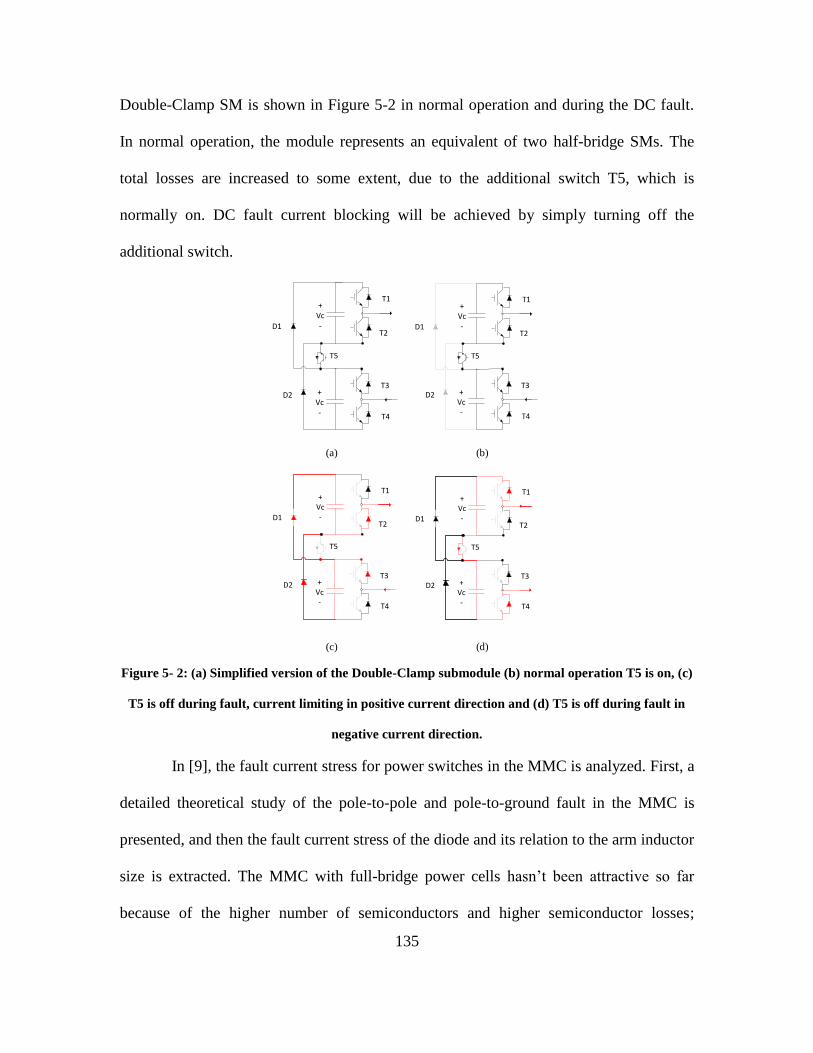
135
Double-Clamp SM is shown in Figure 5-2 in normal operation and during the DC fault.
In normal operation, the module represents an equivalent of two half-bridge SMs. The
total losses are increased to some extent, due to the additional switch T5, which is
normally on. DC fault current blocking will be achieved by simply turning off the
additional switch.
+Vc-
+Vc-
T2
T1
T3
T4
T5
D1
D2
+Vc-
+Vc-
T2
T1
T3
T4
T5
D1
D2
(a) (b)
+Vc-
+Vc-
T2
T1
T3
T4
T5
D1
D2
+Vc-
+Vc-
T2
T1
T3
T4
T5
D1
D2
(c) (d)
Figure 5- 2: (a) Simplified version of the Double-Clamp submodule (b) normal operation T5 is on, (c)
T5 is off during fault, current limiting in positive current direction and (d) T5 is off during fault in
negative current direction.
In [9], the fault current stress for power switches in the MMC is analyzed. First, a
detailed theoretical study of the pole-to-pole and pole-to-ground fault in the MMC is
presented, and then the fault current stress of the diode and its relation to the arm inductor
size is extracted. The MMC with full-bridge power cells hasn’t been attractive so far
because of the higher number of semiconductors and higher semiconductor losses;

136
however, more studies on the AAC and its ride-through capability of DC fault is
currently ongoing. The AAC consists of two substantial parts: (i) Cascaded N series H-
bridge sub-modules (SMs); (ii) direction switches (DS), composed of series of IGBTs
with antiparallel diodes. Each phase has two arms, conducting alternately. Each arm is
comprised of a DS and CHB [21]. A comprehensive study of the DC fault ride-through
capability of the AAC and its STATCOM mode of operation is carried out in [61],[104-
107] A detailed control structure and comprehensive study of the DC fault blocking of
the AAC and the MMC-FB is still not available in the literature.
5.3 DC Fault Analysis of MMC Full-Bridge and AAC
For simplicity, as shown in Figure 5-3, a three-phase, grid-tied MMC with full-
bridge cell and an AAC with a single module per arm are considered for analysis during
the pole-to-pole DC fault. The protection command for clearing the DC fault in this
analysis is to turn off all the IGBTs throughout the converter. By turning off the director
switches, the current will be passed through the antiparallel diode, and the rest of the
circuit will be the same for both the MMC with full-bridge cells and the AAC. Since the
MMC-FB and AAC have the same model during the DC fault, the extracted model will
be valid for both; however, the dynamic will be different due to the different designs of
the arm inductors and the power cell capacitors.

137
vdc
Va
Vb
Vc
La
Lb
Lc
Larm
Larm
vuA+-
vlA+-
(a)
Va
Vb
Vc
La
Lb
Lc
Larm
Larm
vcuA+-
vclA+-
vdc
DS
DS
(b)
Figure 5- 3: A three- phase grid tied (a) MMC with Full-Bridge cell, (b) AAC
To analyze the fault, the following definition of voltage and current in the MMC
and AAC is considered.
The AC source voltage is considered as:
)sin( tVv mA (5-1)
Where, is the phase difference between grid voltage and the pole voltage of the
MMC. The phase voltage and current of the MMC is expressed as:
)sin( tVv mao (5-2)
)sin( tIi mao (5-3)
Where ,2
dcm
VmV . By defining the output voltage, the reference voltage of the
upper and lower arm for the MMC and AAC are defined as:

138
)sin(2
tVV
v mdc
ua (5-4)
)sin(2
tVV
v mdc
ua (5-5)
And the upper and lower arm current will consist of the DC current and phase
current in the AAC. In the case of the MMC full-bridge, the circulating current will be
added to the arm currents. By assuming a balanced three-phase, and identical components
in each arm, the upper and lower arm currents can be defined as:
)(23
ciraodc
ua iii
i (5-6)
)(23
ciraodc
ua iii
i (5-7)
After defining the converter voltage and currents, the converter DC fault model
can be analyzed in the next step. The all fault period of the converter up to the fault
current clearance time is divided into three parts:
Va
Vb
Vc
La
Lb
Lc
Larm
Larm
vcuA+-
vcuL+-
Figure 5- 4: DC Fault path through the antiparallel diodes

139
Va
Vb
Vc
La
Lb
Lc
Larm
Larm
vcuA+-
vcuL+-
Figure 5- 5: DC Fault path at the final stage of fault clearance
5.3.1 During Fault Detection Time (t0 to t1)
The fault detection time is defined from the time that the actual fault happens up
to the time that the fault is declared inside the converter and the protection process is
begun. This time, which is typically about a microsecond to a millisecond, depends on
the delay time of the voltage and current sensors and the processor, and the defined
maximum fault voltage and current within the converter. The current through the
converter will be increased and the capacitors will be discharged within the normal
operation of the MMC-FB and AAC during DC fault. During normal operation of the
MMC with FB power cells, the sum of the upper and lower voltages is equal to the DC
side voltage. This is true on the condition that the negative voltage generation of the full-
bridge is not required in order to have voltage greater than DC voltage at the output of the
converter and that the operation of the MMC with full-bridge cells is similar to the
conventional half-bridge MMC.
During the fault detection time, the upper and lower arm currents of phase a are
obtained as follows:

140
)(232
)()( 01
11 tt
L
VVititi
arm
lAuAdcauA
(5-8)
)(232
)()( 01
11 tt
L
VVititi
arm
lAuAdcalA
(5-9)
According to equations (5-8) and (5-9), during fault detection the upper and lower
arm will be increased depending on the arm inductor size and the sum of upper and lower
arm voltages.
5.3.2 During IGBT’s Turned-off Time in Which Fault Currents Flow
Through Diodes (t1 to t2)
After detecting the fault through the fault detection algorithm within the control
processor of the converter, the simple command for the MMC-FB and the AAC is to set
all the IGBTs to be turned-off. The current path through the diodes is shown in Figure 5-
4. In this situation, the capacitor voltage will be connected in the arm negatively and the
DC fault current will be blocked by the negative voltage of the capacitors. The upper and
lower arm current at this time is shown in (5-10) and (5-11):
)(2
)()( 1212 ttL
VVtiti
arm
clAcuAuAuA
(5-10)
)(2
)()( 1212 ttL
VVtiti
arm
clAcuAlAlA
(5-11)
The fault path through the antiparallel diodes of SM makes the capacitor voltages
drop negatively, and this will prevent the DC fault current from increasing further.

141
5.3.3 During Fault Currents’ Flow Through Diodes and the Fault Current
Blocking Time (t2 to t3)
During fault current blocking time, the current passes through the upper or lower
arm of the phase, depending on the operational point of the converter, and the arm current
returns through the other phase arm as shown in Figure 5-5 until the fault current reaches
zero. During this time, the arm current can be obtained by:
)(2
)()( 2323 ttL
VVtiti
arm
clBcuAuAuA
(5-12)
The complete blocking of the DC fault current will occur whenever the total
voltage of the capacitors in the fault path become higher than the line-to-line AC voltage.
Therefore, the time of complete DC fault current clearance corresponds with the
following condition:
acstackCstackA vvv (5-13)
The fault current waveform during each time interval up to the complete DC fault
clearance for both the MMC with full-bridge power cells and the AAC is shown in Figure
5- 6.
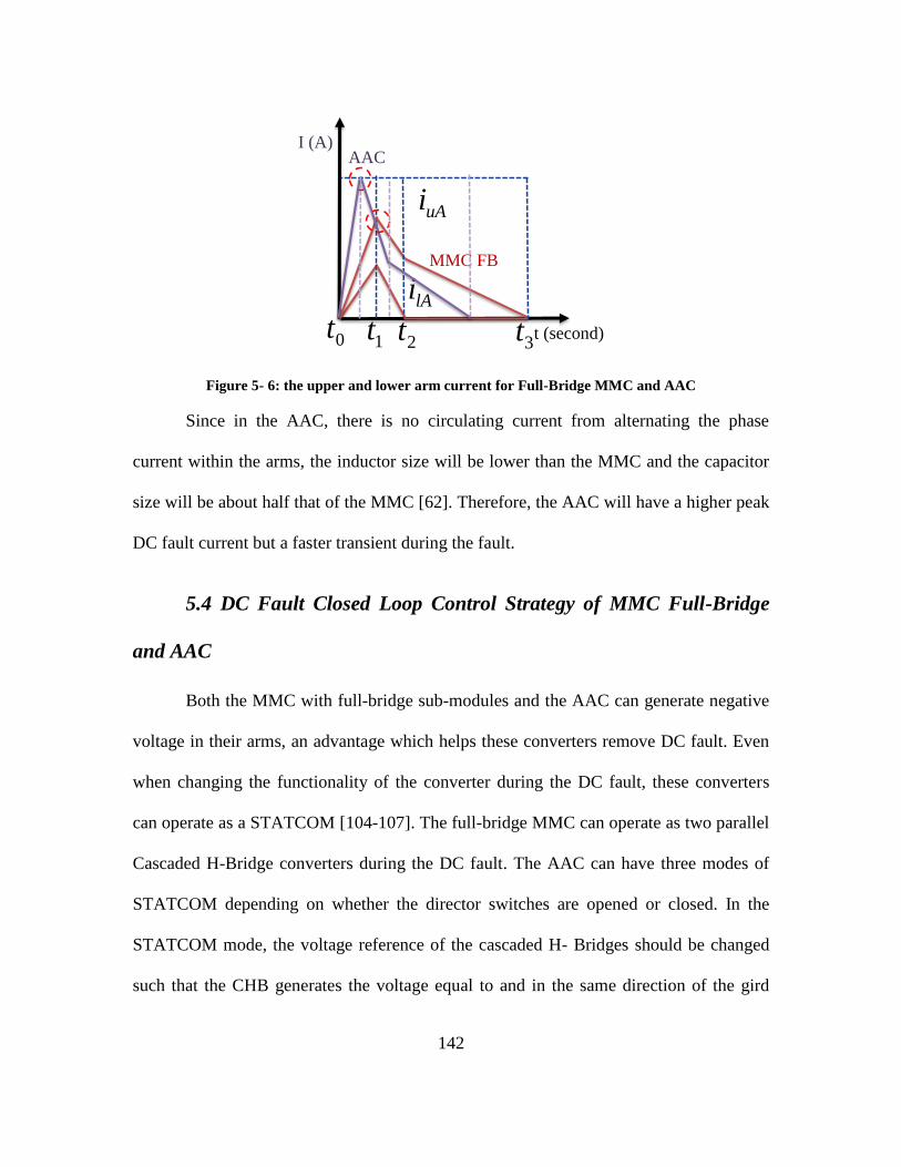
142
Figure 5- 6: the upper and lower arm current for Full-Bridge MMC and AAC
Since in the AAC, there is no circulating current from alternating the phase
current within the arms, the inductor size will be lower than the MMC and the capacitor
size will be about half that of the MMC [62]. Therefore, the AAC will have a higher peak
DC fault current but a faster transient during the fault.
5.4 DC Fault Closed Loop Control Strategy of MMC Full-Bridge
and AAC
Both the MMC with full-bridge sub-modules and the AAC can generate negative
voltage in their arms, an advantage which helps these converters remove DC fault. Even
when changing the functionality of the converter during the DC fault, these converters
can operate as a STATCOM [104-107]. The full-bridge MMC can operate as two parallel
Cascaded H-Bridge converters during the DC fault. The AAC can have three modes of
STATCOM depending on whether the director switches are opened or closed. In the
STATCOM mode, the voltage reference of the cascaded H- Bridges should be changed
such that the CHB generates the voltage equal to and in the same direction of the gird
lAi
1t0t 2t
AAC
MMC FB
3t
uAi
I (A)
t (second)

143
voltage. This chpater concerns only the medium voltage application of the MMC and
AAC . So the ability of the converter to inject reactive power to the grid is no longer of
interest. However, a control strategy corresponding with the output closed-loop control of
the converter is required during the fault, mainly to maintain the capacitor voltage at a
specified value and limit the DC fault current. The closed-loop control of the MMC with
H-Bridge cells and the AAC during the DC fault is shown in Figure 5-7.
-
+
+
-
PI
PI
W(L+Larm)
+-
-+
+
-
Va
Vb
Vc
CPS-
PWM
Pulses
Isdref
Isqref
IsdInv d-qTrans
vPjk vNjk
Voltage
Balance (a) & Circulating
current control
(b)
iPjiNj
Vsd
Vsq
Isq
PIV cref
Vc
+ -
W(L+Larm)
+1:ip, iN>0
-1:ip, iN<0-
Vcref
vcj
+vref_j
K ±1
(a)
Vref_ccsciP
iN
12 PR-
+0 (b)
Figure 5- 7: The closed-loop control of FB MMC and AAC during the DC Fault
Control strategy during the fault is similar to the closed-loop control of the MMC
and AAC [63], except in this situation the d axis reference current is about zero and it is
fed by capacitor voltage control loop to maintain the capacitor voltage of each SM at its
nominal value. In this mode, the capacitor voltage balance control and circulating current
are design requirements for stable operation of the converter during the fault. Since there
is no requirement to inject reactive power to the grid in the medium voltage DC
application, the reference of the q axis current is set to zero. The polarity of the d-q axis
current can be changed in inverter or rectifier operation mode of the converter.

144
Table 5- 1: Case study MMC with FB and AAC specifications
Parameters MMC-FB AAC
Power rate 600kW 600kW
DC Line Voltage 5kV 4kV
Line to Line Voltage 3.3 kV 3.3 kV
RL grid 1Ω 1mH 1Ω 1mH
Switching Frequency 1kHz 1kHz
Module Rated Voltage 637 V 637 V
No of Module 8 4
Pole Voltage Levels 9 9
Cell Cap size for ΔV<40 6mF 3mF
Arm Inductor 3mH 600mH
5.5 Simulation Result
In this section, the operation of the MMC with full-bridge power cells and the
AAC with closed-loop control under DC fault is simulated using Simulink/Matlab. To
provide an accurate simulation, the DC bus short circuit is modeled by a small resistor
that can be in order of 10 to 0.001 ohms. The converter is operating in grid-tied inverter
mode prior to the fault occurrence. The case study parameters are specified as presented
in Table 5-1. The simulation is run for different scenarios, and the following facts are
assumed through the simulation of each fault scenario. First, a time of 10 msec is
considered for a fault detection time, during which period the peak DC fault current takes
place and the power cell capacitor voltage is discharged. Secondly, the short circuit
resistor, Rsc is assumed to be 0.01 Ω, and for ideal conditions, the case with Rsc 10 Ω is

145
simulated as well. A very small inductor is used for a more accurate model of the short
circuit. The assumed DC fault scenario is shown in Figure 5-8. Each of the following
cases are considered for the simulation analysis:
Figure 5- 8: DC Fault scenario for Full-Bridge MMC and AAC
Figure 5- 9: DC Fault simulation under Rsc 10 Ω for MMC-FB
Normal Operation
Inverter Mode
DC Fault
Occurrence
DC Fault
Control
0.2 Sec
10 mSec
Fault Detection
0.21 SecCap
Discharging
Cap Voltage
control
DC Fault Current
0 0.1 0.2 0.3 0.4 0.5 0.6-500
0
500
Time(sec)
Idc (
A)
0 0.1 0.2 0.3 0.4 0.5 0.6-500
0
500
Time(sec)
Id (
A)
0 0.1 0.2 0.3 0.4 0.5 0.6-50
0
50
Time(sec)
Iq (
A)
0 0.1 0.2 0.3 0.4 0.5 0.6-500
0
500
Time(sec)
Iabc (
A)
0 0.1 0.2 0.3 0.4 0.5 0.6200
400
600
Time(sec)
Vcu (
V)
0 0.1 0.2 0.3 0.4 0.5 0.6200
400
600
Time(sec)
Vcl (V
)

146
5.5.1 DC Fault Simulation With Rsc 10 Ω for MMC-FB
For this state, DC fault behavior of the MMC-FB is simulated with the
assumption of using a higher short circuit resistor. The DC fault current, three-phase AC
current, d-q axis current, and cap voltage are shown in Figure 5-9 during the normal
operation and during DC fault. Since the short circuit resistor is high, the 2nd harmonic
circulating current is damped to the zero in a few cycles and the fault clearance time is
soon achieved.
5.5.2 DC Fault Simulation With Rsc 0.01 Ω for MMC-FB
The simulation results of this case are shown in Figure 5-10. A similar scenario
occurs as that shown in Figure 5-8. In this situation, which occurs more often where the
positive and negative rail terminals are connected with fewer fault resistors, the
circulating current will be damping through the oscillatory arm inductor and SM
capacitors. The amount of peak current still depends on the design of the arm inductor
and the capacitor for the MMC, as well as fault detection time.
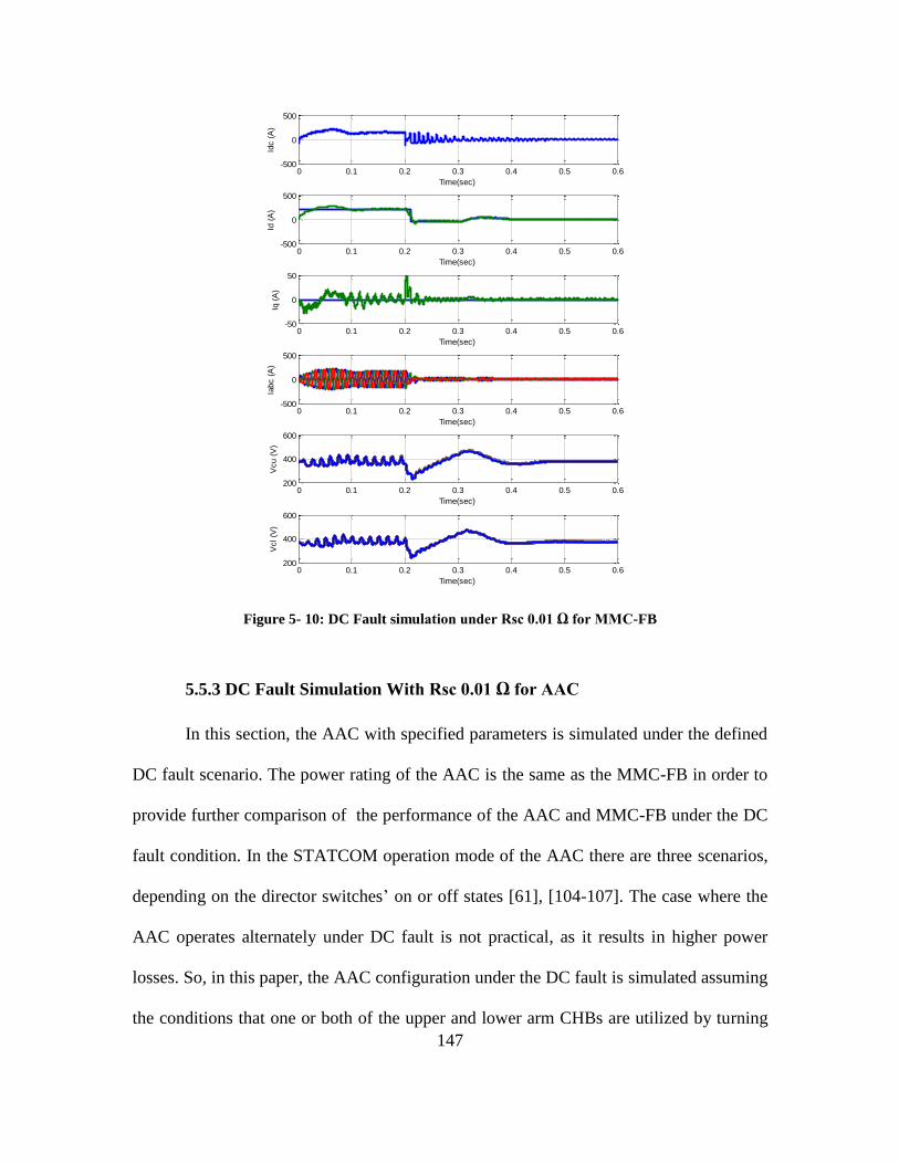
147
Figure 5- 10: DC Fault simulation under Rsc 0.01 Ω for MMC-FB
5.5.3 DC Fault Simulation With Rsc 0.01 Ω for AAC
In this section, the AAC with specified parameters is simulated under the defined
DC fault scenario. The power rating of the AAC is the same as the MMC-FB in order to
provide further comparison of the performance of the AAC and MMC-FB under the DC
fault condition. In the STATCOM operation mode of the AAC there are three scenarios,
depending on the director switches’ on or off states [61], [104-107]. The case where the
AAC operates alternately under DC fault is not practical, as it results in higher power
losses. So, in this paper, the AAC configuration under the DC fault is simulated assuming
the conditions that one or both of the upper and lower arm CHBs are utilized by turning
0 0.1 0.2 0.3 0.4 0.5 0.6-500
0
500
Time(sec)
Idc (
A)
0 0.1 0.2 0.3 0.4 0.5 0.6-500
0
500
Time(sec)Id
(A
)
0 0.1 0.2 0.3 0.4 0.5 0.6-50
0
50
Time(sec)
Iq (
A)
0 0.1 0.2 0.3 0.4 0.5 0.6-500
0
500
Time(sec)
Iabc (
A)
0 0.1 0.2 0.3 0.4 0.5 0.6200
400
600
Time(sec)
Vcu (
V)
0 0.1 0.2 0.3 0.4 0.5 0.6200
400
600
Time(sec)
Vcl (V
)

148
both on or via the DS, and that alternating between the upper and lower arms no longer
exists. To have the same conditions for the MMC-FB, the AAC under fault is considered
to be transformed to two parallel CHBs, which in this mode causes DC fault blocking
time to be faster. The simulation result is shown in Figure 5-11 for the DC current, d-q
axis output current, three-phase currents, and the capacitor voltages. The upper and lower
arm currents are shown in Figure 5-12 as well.
Figure 5- 11: DC Fault simulation under Rsc 0.01 Ω for AAC
0 0.1 0.2 0.3 0.4 0.5 0.6-1000
0
1000
Time(sec)
Idc (
A)
0 0.1 0.2 0.3 0.4 0.5 0.6 0.7-500
0
500
Time(sec)
Id (
A)
0 0.1 0.2 0.3 0.4 0.5 0.6 0.7-50
0
50
Time(sec)
Iq (
A)
0 0.1 0.2 0.3 0.4 0.5 0.6 0.7-500
0
500
Time(sec)
Iabc (
A)
0 0.1 0.2 0.3 0.4 0.5 0.6 0.7500
600
700
Time(sec)
Vcu (
V)
0 0.1 0.2 0.3 0.4 0.5 0.6 0.7500
600
700
Time(sec)
Vcl (V
)

149
Figure 5- 12: DC Fault interruption simulation under Rsc 0.01 Ω for MMC-FB
5.5.4 DC Fault Interrupt Simulation With Rsc 0.01 Ω for MMC- FB
Some of the DC faults would be removed after some cycles. Therefore, the
normal operation of the converter after the fault clearance is of concern. Hence, in this
section, the DC fault interrupt and normal operation of the converter after the DC fault is
illustrated. In this scenario, the DC fault is going to be removed after 0.5sec and the DC
fault has occurred, as seen in Figure 5-8, prior the fault clearance. In Figure 5-13, the DC
fault interrupt simulation result for the DC fault current, the d-q axis, and three- phase
output current and the capacitor voltages are shown.
0 0.1 0.2 0.3 0.4 0.5 0.6 0.7-500
0
500
Time(sec)
Idc (
A)
0 0.1 0.2 0.3 0.4 0.5 0.6 0.7-500
0
500
Time(sec)
Id (
A)
0 0.1 0.2 0.3 0.4 0.5 0.6 0.7-50
0
50
Time(sec)
Iq (
A)
0 0.1 0.2 0.3 0.4 0.5 0.6 0.7-500
0
500
Time(sec)
Iabc (
A)
0 0.1 0.2 0.3 0.4 0.5 0.6 0.7200
400
600
Time(sec)
Vcu (
V)
0 0.1 0.2 0.3 0.4 0.5 0.6 0.7200
400
600
Time(sec)
Vcl (V
)
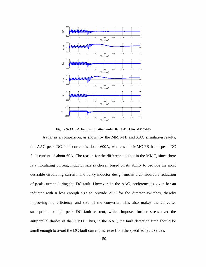
150
Figure 5- 13: DC Fault simulation under Rsc 0.01 Ω for MMC-FB
As far as a comparison, as shown by the MMC-FB and AAC simulation results,
the AAC peak DC fault current is about 600A, whereas the MMC-FB has a peak DC
fault current of about 60A. The reason for the difference is that in the MMC, since there
is a circulating current, inductor size is chosen based on its ability to provide the most
desirable circulating current. The bulky inductor design means a considerable reduction
of peak current during the DC fault. However, in the AAC, preference is given for an
inductor with a low enough size to provide ZCS for the director switches, thereby
improving the efficiency and size of the converter. This also makes the converter
susceptible to high peak DC fault current, which imposes further stress over the
antiparallel diodes of the IGBTs. Thus, in the AAC, the fault detection time should be
small enough to avoid the DC fault current increase from the specified fault values.
0 0.1 0.2 0.3 0.4 0.5 0.6 0.7 0.8-500
0
500
Time(sec)
IuA
0 0.1 0.2 0.3 0.4 0.5 0.6 0.7 0.8500
600
700
Time(sec)
VcuA
0 0.1 0.2 0.3 0.4 0.5 0.6 0.7 0.8-500
0
500
Time(sec)
IlA
0 0.1 0.2 0.3 0.4 0.5 0.6 0.7 0.8500
600
700
Time(sec)
VclA
0 0.1 0.2 0.3 0.4 0.5 0.6 0.7 0.8-500
0
500
Time(sec)
Ia
0 0.1 0.2 0.3 0.4 0.5 0.6 0.7 0.8-1000
0
1000
Time(sec)
Idc
151
5.6 Conclusions
In this chapter, the DC fault ride-through capability of the MMC, particularly the
MMC with full-bridge power cells, and the recently developed AAC is investigated.
Theoretical fault analysis is performed to show the intrinsic ability of the MMC with full-
bridge cells to contain the DC-side short-circuit fault current. Then, closed-loop control
of the MMC-FB and AAC is employed during the DC fault to substantially control the
capacitor voltage and provide fault current limit. The simulation is carried out to illustrate
the performance of the converters’ operation during the DC fault in the MMC-FB and the
AAC. Simulation results show that the AAC, since it has a lower arm inductor and power
cell capacitor in its structure, has a faster transient response; however, it suffers from
higher peak DC fault current. The simulation is performed for a high and low short-
circuit resistor and for the case where there is a DC fault interrupt, the operation of the
converter is shown with the adopted DC fault current control. The DC fault blocking
capability of the MMC-FB and the AAC is a promising factor for providing intrinsic DC
fault-blocking in high and medium voltage applications.

152
Chapter 6 Summary, Conclusions and Future Work
6.1 Summary
In this thesis, modeling, control, and design consideration was performed for the
modular multilevel converters with the main focus on the Alternate Arm Converter
(AAC) and the MMC with half-bridge power cells. The basic principles of the formation
of MMC’s and the second generation of the modular multilevel converters, called hybrid
Alternat Arm Converters, was discussed. The mathematical approach for modeling the
behavior of the converter was extracted and the switching, average, and DQ model of the
MMCs were obtained. Then, the closed-loop control approach of the MMC and the AAC
was illustrated and the average and individual capacitor voltage balance control were
shown. The existence of circulating current in the MMC was discussed for and the
Circulating Current Suppressing Control (CCSC) was designed using the Proportional
Quasi-Resonant (PQR) controller. In chapter 4, design considerations for MMCs were
presented. The reliabiltiy-oriented capacitor bank design for MMCs using the Markov-
State Space model was discussed. The design of the arm inductor and capacitor bank was
explained and the optimum switching frequency analysis of the MMCs was carried out
by investigating the reliability of the converter. One of the important factors for the AAC
is the operation of the Director Switches (DS) within the converter. Hence, the Zero
Current Switching operation of the DS for the AAC was illustrated and the design of the

153
arm inductor for the AAC was presented. The main advantage of the AAC over the MMC
with half-bridge power cells is the DC fault ride-through capacbility, which can be
attained by full-bridge power cells. The DC-fault ride-through capabilities of the AAC
and the MMC with full-bridge cells were studied and the DC-fault control approach for
medium voltage application of the AAC and the MMC with FB cells were proposed. The
performed mathematical analysis was verified by the simulation analysis using
MATLAB/SIMULINK in each part.
6.2 Conclusions
The main contributions of this work are presented as follows with the
corresponding conclusions:
1- The DQ model of the modular multilevel converter can be obtained from the
average model to ease the design of the controller. The AAC average model has director
switch functionality, but the average model and the DQ model of the AAC also has
nonlinear complications.
2- The control method for the AAC is expanded upon, based on the same control
approach used for the MMC with half-bridge cells.
3- High reliability capacitor bank design for the MMCs was done using
component and system-level reliabiltiy modeling. The Markov model is proposed for use
in modeling the capacitor bank for the MMC. The reliability function of the capacitor
bank was extracted and compared for three different capacitor bank designs using
Aluminium Electrolytic and film capacitors. Using the Markov model, the failure rate of
154
the system for each case was estimated and, finally, a comparison among the results of
the reliability modeling of the systems was performed using the following three reliability
modeling techniques: part-count, combinatorial, and Markov model. The results show
that reliability modeling using the Markov model tends to be closeest to the realistic
reliability model of the system.
4- The reliability oriented switching frequency analysis for the modular multilevel
converters was carried out. The stress analysis of the MMC for phase-arm currents and
voltages, as well as the converters’ output voltage and current, was done along with an
evaluation of the impact of switching frequencies harmonic components in the low
switching rate. The effect of a circulating current suppressing controller was also
investigated. The switching frequency evaluation showed an optimum point favoring a
medium switching rate, as the circulating current harmonic content was seen to increase
at lower frequencies, resulting in heightened conduction losses for the devices and a
higher voltage ripple for the power-cell capacitors.
5- A design and switching power losses comparison between the AAC and half –
bridge MMC in a sample case study was done. The results show that the AAC, despite
having a higher number of switches, will have fewer switching power losses, mainly due
to the lack of circulating current and load power alternating. However, AACs also suffer
from high switching power losses in the director switches.
6- The DC fault ride-through capability of the MMC, particularly for the MMC
with full-bridge power cells, and the recently developed AAC was investigated.
Theoretical fault analysis was performed to show the intrinsic ability of the MMC with
full-bridge cells to contain the DC-side short-circuit fault current. Closed-loop control of

155
the MMC-FB and the AAC was then employed during the DC fault to substantially
control the capacitor voltage and provide fault current limit. The simulation result was
carried out to illustrate the performance of the converter’s operation during the DC fault
in the MMC-FB and the AAC. Simulation results show that since the AAC has lower arm
inductor and power cell capacitors in its structure, it has a faster transient response.
However, it also suffers from higher peak DC fault current. The simulation was
performed for high and low short-circuit resistors and for the case where there is a DC
fault interrupt, the operation of the converter is shown with the adopted DC fault current
control. The DC fault blocking capability of the MMC-FB and the AAC is promising, as
it provides intrinsic DC fault for these converters in high and medium voltage
applications.
6.3 Future Work
In order to finish the study on MMCs with regard to modeling, control and design
considerations, as well as the DC fault ride-through capabiltiy of the MMC, the following
works should be conducted in the future:
1) Nonlinear modeling of the AAC to attain the average and the DQ model along
with additional analysis in order to understand the interaction between the arm
quantities.
2) Study of new control techniques to evaluate the required overalp time for the
AAC.
3) Experimental verfication of the proposed analysis and methods for the AAC
and the MMC.
156
4) Reliability modeling verification of the capacitor bank in practice, using
acceleration tests.
5) AAC hardware setup testing to verify the operation of the AAC and the
validity analysis of the utilized control techniques for the capacitor voltage
balance and the overlap time.
6) Switching frequency design verifictaion of the MMC taking into consideration
the trade-off between the capacitor voltage ripple and semiconductor power
losses.
7) Evaluation of the DC fault control technique proposed for the MMC with FB
and AAC experimental verifiation using the prototype hardware.

157
References
[1] J. Chang, “Advancements and trends of power electronics for industrial
applications,” IEEE IECON, vol. 3, pp. 3021-3022, Nov. 2003.
[2] B. K. Bose, “Technology advancement and trends in power electronics,” IEEE
IECON, vol. 3, pp. 3019-3020, Nov. 2003.
[3] R. D. Klug and N. Klaassen, “High power medium voltage drives—Innovations,
portfolio, trends,” in Proc. Eur. Conf. Power Electron. Appl., 2005, pp. 1–10.
[4] B. Wu, High-Power Converters and AC Drives. New York: Wiley-IEEE Press,
Mar. 2006.
[5] P. Steimer, “High power electronics, trends of technology and applications,” in
Proc. PCIM, Germany, May 2007.
[6] L. G. Franquelo, J. Rodriguez, J. I. Leon, S. Kouro, R. Portillo, and M. A. M.
Prats, “The age of multilevel converters arrives,” IEEE Ind. Electron. Mag., vol.
2, no. 2, pp. 28–39, Jun. 2008.
[7] J. Rodriguez, B. Wu, S. Bernet, N. Zargari, J. Rebolledo, J. Pontt, and P. Steimer,
“Design and evaluation criteria for high power drives,” in Conf. Rec. IEEE IAS
Annu. Meeting, Oct. 5–9, 2008, pp. 1–9.
[8] B. K. Bose, “Power electronics and motor drives recent progress and
perspective,” IEEE Trans. Ind. Electron., vol. 56, no. 2, pp. 581–588, Feb. 2009.

158
[9] V. Najmi, S Ebrahimi, H Oraee, “Output voltage quality intensification of diode
clamped multilevel inverters using FM PWM technique”, Power Electronics and
Drive Systems Technology (PEDSTC), 2012 3rd, 98-102.
[10] J Rodriguez, JS Lai, FZ Peng, “Multilevel inverters: a survey of topologies,
controls, and applications”, Industrial Electronics, IEEE Transactions on 49 (4),
pp: 724-738, 2002.
[11] ABB. [Online]. Available: www.abb.com
[12] SIEMENS. [Online]. Available: www.siemens.com
[13] TMEIC-GE. [Online]. Available: www.tmeic-ge.com
[14] Eaton. [Online]. Available: www.eaton.com
[15] Yaskawa. [Online]. Available: www.yaskawa.eu.com
[16] Alstom. [Online]. Available: www.alstom.com
[17] W. McMurray, “Fast response stepped-wave switching power converter circuit,”
U.S. Patent 3 581 212, May 25, 1971.
[18] J. A. Dickerson and G. H. Ottaway, “Transformerless power supply with line to
load isolation,” U.S. Patent 3 596 369, Aug. 3, 1971.
[19] R. H. Baker, “High-voltage converter circuit,” U.S. Patent 4 203 151, May 13,
1980.
[20] R. H. Baker, “Bridge converter circuit,” U.S. Patent 4 270 163, May 26, 1981.
[21] P.W. Hammond, “A new approach to enhance power quality for medium voltage
drives,” in Proc. Ind. Appl. Soc. 42nd Annu. Petroleum Chem. Ind. Conf., Sep.
11–13, 1995, pp. 231–235.

159
[22] T. Meynard and H. Foch, “Dispositif électronique de conversion d’énergie
électrique,” French Patent 267 971 5B1, Jan. 29, 1993.
[23] HVDC-VSC: transmission technology of the future a new hybrid HVDC circuit
technology, Alstom Grid, Spring-Summer 2011.
[24] R. Marquardt, A. Lesnicar, J. Hildinger, “Modulares Stromrichterkonzept für
Netzkupplungsanwendung bei hohen Spannungen,” ETG-Fachtagung, Bad
Nauheim, Germany, 2002.
[25] A. Lesnicar and R. Marquardt, “An innovative modular multilevel converter
topology suitable for a wide power range,” In Proc. IEEE Power Tech. Conf.,
Bologna, Italy, Jun. 2003.
[26] B. Jacobson et al, “VSC-HVDC Transmission with Cascaded Two-Level
Converters”, CIGRÉ Paper B4-110, Paris, 2010.
[27] D. C. Ludois, J. K. Reed, and G. Venkataramanan, "Hierarchical Control of
Bridge-of-Bridge Multilevel Power Converters," Industrial Electronics, IEEE
Transactions on, vol. 57, pp. 2679-2690, 2010.
[28] N.M. MacLeod, A.C. Lancaster, C.D.M. Oates, “The development of a Power
Electronic Building Block for use in Voltage Source Converters for HVDC
transmission applications”, CIGRÉ Colloquium, Bergen, Norway, 2009.
[29] C.C. Davidson, D.R. Trainer, “Innovative Concepts for Hybrid Multilevel
Converters for HVDC Power Transmission” 9th IET International Conference
on AC and DC Power Transmission, pp. 1-5, 2010.
160
[30] G.P. Adam et al “Network Fault Tolerant Voltage-Source-Converters for High-
Voltage Applications”, Paper 0074, IET 9th International Conference on AC and
DC Power Transmission, London, 2010.
[31] R.C.Knight, D.J.Young, D.R.Trainer, “Relocatable GTO-based Static Var
Compensator for NGC Substations”, CIGRÉ paper 14-106, Paris, 1998.
[32] H.P. Mohammadi, M.T. Bina, “A Transformerless Medium-Voltage STATCOM
Topology Based on Extended Modular Multilevel Converters,” IEEE Trans.
Power Electronics, vol. 26, no. 5, pp. 1534 – 1545, 2011.
[33] R. Feldman et al, “A Low Loss Modular Multilevel Voltage Source Converter for
HVDC Power Transmission and Reactive Power Compensation”, Paper 0067,
IET 9th International Conference on AC and DC Power Transmission, London,
2010.
[34] Feldman et al, “Hybrid Modular Multilevel VSC For HVDC Power
Transmission”, IEEE Transactions On Industry Applications, Vol. 49, No. 4,
July/August 2013.
[35] Emmanuel Kwaku Amankwah, “A Parallel Hybrid Modular Multilevel Converter
for High Voltage DC Applications” PhD Dissertation, August, 2013.
[36] M. Merlin, T. Green, P. Mitcheson, D. Trainer, D. Critchley, and R. Crookes, “A
new hybrid multi-level voltage-source converter with dc fault blocking
capability,” presented at the 9th IET Int. Conf. AC DC Power Transm, London,
U.K., Oct. 2010.

161
[37] M. Davies, M. Dommaschk, J. Dorn, J. Lang, D. Retzmann, D. Soerangr, “HVDC
PLUS – Basics and Principle of Operation”, [Online]. Available:
www.siemens.com/energy/hvdcplus.
[38] ABB. (2013). It’s time to connect with offshore wind supplement [Online].
Available: http://www.abb.com/hvdc.
[39] S. Allebrod, R. Hamerski, and R. Marquardt, “New transformerless, scalable
modular multilevel converters for HVDC-transmission,” In Proc. IEEE Power
Electronics Specialists Conf. PESC, pages 174–179, 2008.
[40] M. Hiller, D. Krug, R. Sommer, and S. Rohner, “A new highly modular medium
voltage converter topology for industrial drive applications,” In Proc. 13th
European Conf. Power Electronics and Applications EPE’09, pages 1–10, 2009.
[41] S. Rohner, S. Bernet, M. Hiller, and R. Sommer, “Modelling, simulation and
analysis of a modular multilevel converter for medium voltage applications,” In
Proc. IEEE Int Industrial Technology (ICIT) Conf, pages 775–782, 2010.
[42] M. Hagiwara, H. Akagi, “Control and experiment of pulsewidth-mudulated
Modular Multilevel Converters,” in IEEE Transactions on Power Electronics,
VOL. 24, NO. 7, July 2009.
[43] S.Rohner, S.Bernet, M.Hiller and R.Sommer, “Modulation, Losses, and
Semiconductor Requirements of Modular Multilevel Converters,” in IEEE
transactions on Industrial Electronics, VOL.57, NO.8, August 2010.
[44] Yalong Li, Fred Wang, “Arm Inductance Selection Principle for Modular
Multilevel Converter with Circulating Current Suppressing Control”, in 28th
162
Annual IEEE Applied Power Electronics Conference and Exposition
(APEC2013), pp. 1321-1325, 2013.
[45] Nuntawat Thitichaiworakorn, Makoto Hagiwara,and Hirofumi Akagi,
“Experimental Verification of a Modular Multilevel Cascade Inverter Based on
Double-Star Bridge-Cells (MMCI-DSBC)”, IEEE Transactions on industry
application, pp. 509-519, June 2013
[46] Ilves K., Antonopoulos A., Norrga S., and Nee H.-P., “Steady-state analysis of
interaction between harmonic components of arm and line quantities of modular
multilevel converters”, IEEE Trans. Power Electron., vol. 27, no. 1, pp. 57–68,
Jan. 2012
[47] Qiang Song ; Wenhua Liu ; Xiaoqian Li ; Hong Rao ; Shukai Xu ; Licheng Li ,
“A Steady-State Analysis Method for a Modular Multilevel Converter,” IEEE
Transactions on Power Electronics, pp. 3702-3713, 2013.
[48] Q .R.Tu, Z.xu, and L.Xu, "Reduced Switching-Frequency Modulation and
Circulating Current Suppression for Modular Multilevel Converters," in IEEE
Trans. Power. Del., vo1.26, no.3, July 2011.
[49] Vahid Najmi, Jun Wang, Rolando Burgos, Dushan Boroyevich, “High Reliability
Capacitor Bank Design for Modular Multilevel Converter in MV Applications”,
IEEE Energy Conversion Congress and Exposition (ECCE), pp.1051-1058, 2014.
[50] Vahid Najmi, Jun Wang, Rolando Burgos and Dushan Boroyevich "Reliability
Modeling of Capacitor Bank for Modular Multilevel Converter Based on Markov
State-Space Model", In Proc. of IEEE Applied Power Electronics Conference and
Exposition (APEC), 2015, in press.

163
[51] Vahid Najmi, Hamed Nademi, Rolando Burgos, “An Adaptive Backstepping
Observer for Modular Multilevel Converter,” In Proc. IEEE Energy Conversion
Congress and Exposition (ECCE), pp. 2115- 2120, 2014.
[52] Jun Wang et al, “State-Space Switching Model of Modular Multilevel
Converters,” In 2013 IEEE 14th Workshop on Control and Modeling for Power
Electronics (COMPEL), pages 1–10, 2013.
[53] S. Rohner, J. Weber and S. Bernet, “Continuous Model of Modular Multilevel
Converter with Experimental Verification,” In the IEEE Energy Conversion
Congress and Exposition (ECCE), pp. 4021 – 4028, 2011.
[54] L. Harnefors, S. Norrga, A. Antonopoulos, and H. P. Nee, "Dynamic modeling of
modular multilevel converters," In Power Electronics and Applications (EPE
2011), Proceedings of the 2011-14th European Conference on, 2011, pp. 1-10.
[55] H. Nademi, A. Das, L. Norum, “An analytical frequency-domain modeling of a
Modular Multilevel Converter”, in IEEE Power Electronics and Drive Systems
Technology (PEDSTC), pp. 86-91, 2012.
[56] M.A. Perez, S. Bernet, J. Rodrigues, S. Kouro, R. Lizana, “Circuit
Topologies, Modelling, Control Schemes and Applications
of Modular Multilevel Converters,” In IEEE Early Access Transactions on Power
Electronics, issue 99, 2014.
[57] D.Ludois and G.Venkataramanan, “Simplified Terminal Behavioral Model for a
Modular Multilevel Converter,” In IEEE Transactions on Power Electronics, Vol.
29, No. 4, April 2014.

164
[58] X.She, A. Huang, X. Ni and R.Burgos, “AC Circulating Currents Suppression in
Modular Multilevel Converter”, 38th Annual Conference on IEEE Industrial
Electronics Society, Montreal, Canada, 2012.
[59] C.C. Davidson, A.C. Lancaster, A.J. Totterdell, C.D.M Oates, “A 24 MW Level
Voltage Source Converter Demonstrator to evaluate Different Converter
Topologies”, CIGRE 2012.
[60] A. Nami, J. Liang, F. Dijkhuizen and G. Demetriades, “Modular Multilevel
Converter for HVDC Applications: Review on Converter Cells and
Functionalities”, IEEE TRANSACTIONS ON POWER ELECTRONICS, VOL.
30, NO. 1, JANUARY 2015.
[61] M. Merlin, T. Green, P. Mitcheson, D. Trainer, D. Critchley, and R. Crookes,
“The Alternate Arm Converter: A New Hybrid Multilevel Converter with DC-
Fault Blocking Capability”, IEEE TRANSACTIONS ON POWER DELIVERY,
VOL. 29, NO. 1, FEBRUARY 2014.
[62] M.M.C. Merlin, T.C. Green, P.D. Mitcheson, F.J. Moreno, K.J. Dyke, D.R.
Trainer, “Cell Capacitor Sizing in Modular Multilevel Converters and Hybrid
Topologies”, 16th European Conference on Power Electronics and Applications
(EPE'14-ECCE Europe), pp. 1-10, 2014.
[63] M. Hagiwara, R. Maeda, and H. Akagi, “Control and analysis of the modular
multilevel cascade converter based on double-star chopper-cells (MMCCDSCC),”
IEEE Transactions on Power Electronics, vol. 26, no. 6, pp. 1649-1658, June
2011.
165
[64] E. Wolfgang, "Examples for failures in power electronics systems," presented at
ECPE Tutorial on Reliability of Power Electronic Systems, Nuremberg, Germany,
Apr. 2007.
[65] J. Kolb, F.Kammerer, Michael Braun, “Dimensioning and design of a Modular
Multilevel Converter for Drive applications”, in 15th International Power
Electronics and Motion Control Conference, EPE-PEMC 2012, pages 1-8.
[66] H.Barnklau, A.Gensior and S.Bernet, “Submodule Capacitor Dimensioning for
Modular Multilevel Converters”, in Energy Conversion Congress and Exposition
(ECCE), 2013, pp. 4172-4179.
[67] K.Ilves, S. Norrga, L. Harnfors and H. Nee, “On Energy Storage Requirement in
Modular Multilevel Converters”, in IEEE Transactions on Power Electronics,
VOL.29, NO. 1, January 2014.
[68] Yantao Song and Bingsen Wang, “Survey on Reliability of Power Electronic
Systems”, IEEE Transactions on Power Electronics, Vol. 28, No. 1, January 2013.
[69] F.Richardeau, T.T.L.Pham “Reliability Calculation of the Multilevel Converters:
Theory and Applications” in IEEE transitions on the Industrial Electronics, Vol.
60, NO.10, October 2013.
[70] R. Grinberg, G. Riedel, A. Korn, P. Steimer, and E. Bjornstad, "On reliability of
medium voltage multilevel converters," in Energy Conversion Congress and
Exposition (ECCE), 2013 IEEE, 2013, pp.
[71] H.Wang, F.Blaabjerg, “reliability of capacitors for DC-Link applications-An
overview”, in Energy Conversion Congress and Exposition (ECCE), 2013, pp.
1866-1873.
166
[72] H.Wang, M.Liserre, F.Blaabjerg, et al., “Transitioning to Physics-of Failure as a
Reliability Driver in Power Electronics”, in IEEE Journal of Emerging and
Selected Topics in Power Electronics, VOL.2, NO. 1, March 2014.
[73] R. Marquardt, A. Lesnicar, and J. Hildinger, “Modulares stromrichterkonzept f ür
netzkupplungsanwendungen bei hohen spannungen”, ETG Conference, 2002.
[74] L.M. Cunico, Y.R. De Novaes, A. Nied, S.V.G. Oliveira, “Inner Current Control
Method for Modular Multilevel Converter Applied in Motor Drive”, 10th
IEEE/IAS International Conference on Industry Applications (INDUSCON),
pp.1-8, 2012.
[75] Type 450C 105 °C Ultra-Ripple, Long-life, Inverter Grade and Radial Leaded,
online available in CORNELL DUBILIER Website,
http://www.cde.com/products/aluminum-electrolytic/
[76] “Power Film Capacitor Application Guide,” in CORNELL DUBILIER
Application Notes.
[77] Type 947C Polypropylene Film Capacitor, DC-Link Capacitors, Cornell Dubilier,
and Website in http://www.cde.com/catalogs/947C.pdf
[78] “Capacitors for Power Electronics”, ELECTRONICON Application Notes, 2009.
[79] “Power Electronics Film Capacitors,” in KEMET Application Notes.
[80] MIL-HDBK-217FN2. Military Handbook for Reliability Prediction of Electronics
Equipment. Department of Defence, USA, 1995.
[81] “RIAC-HDBK-217Plus”, Handbook of 217PlusTM Reliability Prediction
Models, 2006.
167
[82] S. G. Parler, Jr., P.E. “Reliability of CDE Aluminum Electrolytic Capacitors.”
CDE Application Note.
[83] Ricky W. Butler and Sally C. Johnson “Techniques for Modeling the Reliability
of Fault-Tolerant Systems with the Markov State-Space Approach” NASA
Reference Publication, 1995.
[84] Jan Pukite, Paul Pukite, “Modeling for Reliability Analysis: Markov Modeling for
Reliability, Maintainability, Safety, and Supportability Analyses of Complex
Systems”, Wiley-IEEE Press, 1998.
[85] G.S. Konstantinou, V.G. Agelidis, “Performance Evaluation of Half-Bridge
Cascaded Multilevel Converters Operated with Multicarrier Sinusoidal PWM
Techniques”, 4th IEEE Conference on Industrial Electronics and Applications,
2009. ICIEA 2009.
[86] D.W. Kang, W.K. Lee, D.S. Hyun, “Carrier rotation strategy for voltage
balancing in flying capacitor multilevel inverter,” IEE Proc. Elect. Power
Applicat. , Vol. 151, pp. 239-248, March 2004.
[87] B.S. Jin, W.K.Lee, T.J. Kim, D.W.Kang, D.S. Hyun, “A study on the multicarrier
PWM methods for voltage balancing of flying capacitor in the flying capacitor
multilevel inverter,” in Proc. of IEEE Int. Conf. Ind. Electron. Soc., 2005, 6pp.
[88] Y.Li, Fred Wang “Analysis on Fault Current Stress for Power Switches in MMC
based DC System” UTK, 2013.
[89] Holmes, D. and Lipo, T. (2003). Pulse Width Modulation for Power Converters:
Principles and Practice. IEEE Press Series on Power Engineering. John Wiley &
Sons.
168
[90] Michael Salcone, Joe Bond, “Selecting Film Bus Link Capacitors for High
Performance Inverter Applications”, Electronic Concepts Inc.report 2009.
[91] IEEE Std 519, IEEE Recommended Practices and Requirements for Harmonic
Control in Electrical Power Systems, New York, NY: IEEE.
[92] A. Korn, M. Winkelnkemper, P. Steimer, “Low Output Frequency Operation of
the Modular Multilevel Converter”, in Proceeding of the IEEE Energy
Conversion Congress and Exposition (ECCE), 2010, pp.3993-3997.
[93] A.Antonopoulos, L.Ängquist, S.Norrga, K.Ilves, L.Harnefors and Hans-Peter
Nee, “Modular Multilevel Converter AC Motor Drives with Constant Torque
from Zero to Nominal Speed”, IEEE TRANSACTIONS ON INDUSTRY
APPLICATIONS, VOL. 50, NO. 3, MAY/JUNE 2014.
[94] Uwe DROFENIK, Johann W. KOLAR, “A General Scheme for Calculating
Switching- and Conduction-Losses of Power Semiconductors in Numerical
Circuit Simulations of Power Electronic Systems”, Proceedings of the 2005
International Power Electronics Conference (IPEC’05), pp. 4-8, 2005.
[95] Jun Wang, Vahid Najmi, Rolando Burgos, Dushan Boroyevich “Reliability-
Oriented IGBT Selection for High Power Converters,” In Proc. of IEEE Applied
Power Electronics Conference and Exposition, 2015, in press.
[96] D. Schmitt, Y. Wang ,Th. Weyh, R. Marquardt, “DC-Side Fault Current
Management in extended Multiterminal-HVDC-Grids” 9th International Multi-
Conference on Systems, Signals and Devices, 2012.

169
[97] B. Gemmell, J. Dorn, D. Retzmann, and D. Soerangr, “Prospects of multilevel
VSC technologies for power transmission,” in Proc. IEE Transm. Distrib. Conf.
Expo., Apr. 2008, pp. 1–16.
[98] N. Ahmed, S. Norrga, H. P. Nee, A. Haider, D. V. Hertem, L. Zhang, and L.
Harnefors, “HVDC supergrids with modular multilevel converters– The power
transmission backbone of the future,” in Proc. 9th Int. Multi-Conf. Syst., Signals
Devices, 2012, pp. 1–7.
[99] C. Franck, “HVDC circuit breakers: A review identifying future research needs,”
IEEE Trans. Power Del., vol. 26, no. 2, pp. 998–1007, Apr. 2011.
[100] H. M. Pirouz, M. T. Bina, and K. Kanzi, "A New Approach to the Modulation and
DC-Link Balancing Strategy of Modular Multilevel AC/AC Converters," in
Power Electronics and Drives Systems, 2005. PEDS 2005. International
Conference on, 2005, pp. 1503-1507.
[101] T. Luth, M.M.C. Merlin, T.C. Green, F. Hassan and C.D. Barker, “High-
Frequency Operation of a DC/AC/DC System for HVDC Applications”, IEEE
Transactions on Power Electronics, vol. 29, No. 8, AUGUST 2014.
[102] R. Marquardt, “Modular multilevel converter: An universal concept for HVDC-
networks and extended DC-bus-applications”, in Proc. Int. Power Electron.
Conf., Jun. 2010, pp. 502–507.
170
[103] R. Marquardt, “Modular multilevel converter topologies with dc-short circuit
current limitation,” in Proc. IEEE 8th Int. Conf. Power Electron. ECCE Asia,
May 2011, pp. 1425–1431.
[104] Pengfei Hu, Daozhuo Jiang, Yuebin Zhou, Jie Guo, Zhiyong Lin and Yiqiao
Liang “Modulation and control of a new alternate arm multilevel converter for
high-voltage direct current system with direct current fault ridethrough
capability”, International Transactions on Electrical Energy Systems, Int. Trans.
Electr. Energ. Syst. 2014; 24, pp. 1017–1033, 2014.
[105] Ralph Feldman, Ewan Farr, Alan J. Watson, Jon C. Clare, Patrick W. Wheeler,
David R. Trainer, R. Will Crookes, “DC fault ride-through capability and
STATCOM operation of a HVDC hybrid voltage source converter” IET Gener.
Transm. Distrib. Vol. 8, Iss. 1, pp. 114–120, 2014.
[106] E.C. Mathew, A. Shukla, “Modulation, Control and Capacitor Voltage Balancing
of Alternate Arm Modular Multilevel Converter with DC Fault Blocking
Capability”, Twenty-Ninth Annual IEEE Applied Power Electronics Conference
and Exposition (APEC), pp. 3329-3336, 2014.
[107] E.M. Farr, R. Feldman, A.J. Watson, R.P. Burgos, J.C. Clare, P.W. Wheeler and
D. Boroyevich, “Alternate Arm Converter (AAC) operation under faulted AC
Grid Conditions” 7th IET International Conference on Power Electronics,
Machines and Drives (PEMD), pp. 1-6, 2014.