Modeling and Calibration of a MEMS Tensile Stage for ... · Modeling and Calibration of a MEMS...
55
Modeling and Calibration of a MEMS Tensile Stage for Elevated Temperature Experiments on Freestanding Metallic Thin Films by Suhas Eswarappa Prameela A Dissertation Presented in Partial Fulfillment of the Requirements for the Degree Master of Science Approved April 2016 by the Graduate Supervisory Committee: Jagannathan Rajagopalan, Chair Liping Wang Yang Jiao ARIZONA STATE UNIVERSITY May 2016
Transcript of Modeling and Calibration of a MEMS Tensile Stage for ... · Modeling and Calibration of a MEMS...

Modeling and Calibration of a MEMS Tensile Stage for Elevated Temperature
Experiments on Freestanding Metallic Thin Films
by
Suhas Eswarappa Prameela
A Dissertation Presented in Partial Fulfillmentof the Requirements for the Degree
Master of Science
Approved April 2016 by theGraduate Supervisory Committee:
Jagannathan Rajagopalan, ChairLiping Wang
Yang Jiao
ARIZONA STATE UNIVERSITY
May 2016

ABSTRACT
Mechanical behavior of metallic thin films at room temperature (RT) is relatively
well characterized. However, measuring the high temperature mechanical properties
of thin films poses several challenges. These include ensuring uniformity in sample
temperature and minimizing temporal fluctuations due to ambient heat loss, in addi-
tion to difficulties involved in mechanical testing of microscale samples. To address
these issues, we designed and analyzed a MEMS-based high temperature tensile test-
ing stage made from single crystal silicon. The freestanding thin film specimens were
co-fabricated with the stage to ensure uniaxial loading. Multi-physics simulations of
Joule heating, incorporating both radiation and convection heat transfer, were carried
out using COMSOL to map the temperature distribution across the stage and the
specimen. The simulations were validated using temperature measurements from a
thermoreflectance microscope.
i

I would like to dedicate this thesis to my family.
ii
ACKNOWLEDGMENTS
I am grateful to Dr. Rajagopalan for giving me the opportunity to work in his lab.
I would like to thank him for his constant support and encouragement in carrying
out this project.
I am grateful to my lab mates, Rohit Sarkar and Ehsan Izadi for providing me with
MEMS samples for carrying out these experiments. Their constant help throughout
my stay has been instrumental in driving this project. I will always treasure the
meaningful and fun discussions we have had in the lab. It was also a great experience
to share lab space with Cole Snider and Abhinav Kowdle Prakash, both of whom
graduated during my stay.
Thanks to George Garcia from PG enterprises and Jerry Eller from ASU for
providing timely help with the gold wire bonding. I am also grateful to Hamsini
Gopalakrishna for providing chemicals used in initial stages of calibration.
I am grateful to Prof. Liping Wang and Jui-Yung Chang for their help with the
thermoreflectance microscope experiments. I have enjoyed collaborating with the
Nano-Engineered Thermal Radiation Group for the calibration studies.
Thanks to my committee members, Dr. Liping Wang and Dr. Yang Jio for taking
the time to participate in this endeavor. I would also like to thank the Center for Solid
State Electronics Research at Arizona State University for access to their facilities.
iii

TABLE OF CONTENTS
Page
LIST OF FIGURES . . . . . . . . . . . . . . . . . . . . . . . . . . . . . . . . . . . . . . . . . . . . . . . . . . . . . . . . vi
CHAPTER
1 INTRODUCTION . . . . . . . . . . . . . . . . . . . . . . . . . . . . . . . . . . . . . . . . . . . . . . . . . . . 2
1.1 Background . . . . . . . . . . . . . . . . . . . . . . . . . . . . . . . . . . . . . . . . . . . . . . . . . . . . 2
1.2 Objectives . . . . . . . . . . . . . . . . . . . . . . . . . . . . . . . . . . . . . . . . . . . . . . . . . . . . . 4
1.3 Approach . . . . . . . . . . . . . . . . . . . . . . . . . . . . . . . . . . . . . . . . . . . . . . . . . . . . . . 5
1.4 Materials Under Study . . . . . . . . . . . . . . . . . . . . . . . . . . . . . . . . . . . . . . . . . . 5
1.5 Structure of the Report . . . . . . . . . . . . . . . . . . . . . . . . . . . . . . . . . . . . . . . . . 5
2 NUMERICAL MODEL FOR JOULE HEATING . . . . . . . . . . . . . . . . . . . . . . 8
2.1 Heat Transfer at the Micro/Nano Scale . . . . . . . . . . . . . . . . . . . . . . . . . . . 8
2.2 COMSOL Multiphysics . . . . . . . . . . . . . . . . . . . . . . . . . . . . . . . . . . . . . . . . . 9
2.3 Mathematical Model . . . . . . . . . . . . . . . . . . . . . . . . . . . . . . . . . . . . . . . . . . . . 10
2.4 Parametric Study . . . . . . . . . . . . . . . . . . . . . . . . . . . . . . . . . . . . . . . . . . . . . . . 12
2.5 Parametric Study - FCC Thin Films . . . . . . . . . . . . . . . . . . . . . . . . . . . . . 15
2.5.1 Aluminum . . . . . . . . . . . . . . . . . . . . . . . . . . . . . . . . . . . . . . . . . . . . . . . 15
2.5.2 Copper . . . . . . . . . . . . . . . . . . . . . . . . . . . . . . . . . . . . . . . . . . . . . . . . . . 18
2.5.3 Nickel . . . . . . . . . . . . . . . . . . . . . . . . . . . . . . . . . . . . . . . . . . . . . . . . . . . 20
2.5.4 Gold . . . . . . . . . . . . . . . . . . . . . . . . . . . . . . . . . . . . . . . . . . . . . . . . . . . . 22
3 CALIBRATION OF THE MEMS STAGE . . . . . . . . . . . . . . . . . . . . . . . . . . . . . 25
3.1 Motivation . . . . . . . . . . . . . . . . . . . . . . . . . . . . . . . . . . . . . . . . . . . . . . . . . . . . . 25
3.2 Thermoreflectance Microscopy . . . . . . . . . . . . . . . . . . . . . . . . . . . . . . . . . . 26
3.3 Thermoreflectance Coefficient . . . . . . . . . . . . . . . . . . . . . . . . . . . . . . . . . . . . 28
3.4 Measuring Sample Temperature . . . . . . . . . . . . . . . . . . . . . . . . . . . . . . . . . . 29
4 EXPERIMENTAL TECHNIQUES. . . . . . . . . . . . . . . . . . . . . . . . . . . . . . . . . . . . 34
iv
CHAPTER Page
4.1 Fabrication of the Device . . . . . . . . . . . . . . . . . . . . . . . . . . . . . . . . . . . . . . . . 34
4.2 Microstructure Characterization . . . . . . . . . . . . . . . . . . . . . . . . . . . . . . . . . 35
4.3 RT Tensile Experiments . . . . . . . . . . . . . . . . . . . . . . . . . . . . . . . . . . . . . . . . . 35
4.4 High Temperature Test Stage . . . . . . . . . . . . . . . . . . . . . . . . . . . . . . . . . . . . 38
5 CONCLUSION . . . . . . . . . . . . . . . . . . . . . . . . . . . . . . . . . . . . . . . . . . . . . . . . . . . . . . 42
5.1 Conclusions . . . . . . . . . . . . . . . . . . . . . . . . . . . . . . . . . . . . . . . . . . . . . . . . . . . . 42
5.2 Limitations . . . . . . . . . . . . . . . . . . . . . . . . . . . . . . . . . . . . . . . . . . . . . . . . . . . . . 43
5.3 Outline for Further Work . . . . . . . . . . . . . . . . . . . . . . . . . . . . . . . . . . . . . . . . 44
REFERENCES . . . . . . . . . . . . . . . . . . . . . . . . . . . . . . . . . . . . . . . . . . . . . . . . . . . . . . . . . . . . 45
v
LIST OF FIGURES
Figure Page
1.1 Nanocrystalline Aluminum Films (reproduced from [11]) . . . . . . . . . . . . . . 3
1.2 In situ Thermo-mechanical Test Set up (reproduced from [12]) . . . . . . . . 4
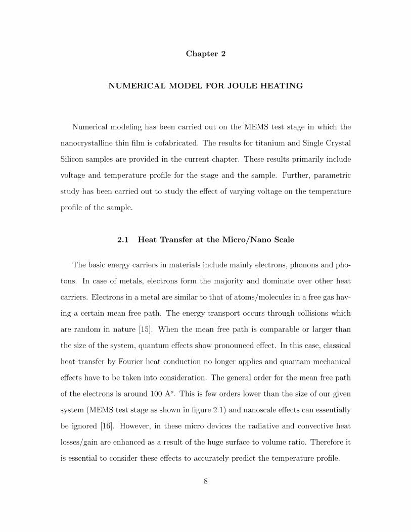
2.1 from left : (a) Basic MEMS Test Stage for the nc Films. (b) Close up
Near the nc Thin Film Sample (reproduced from [3]) . . . . . . . . . . . . . . . . . 9
2.2 from top left : (a) Creating Geometry (b) Setting up Model (c) Apply-
ing Boundary Conditions ; from bottom left : (d) Meshing (e) Result
:Voltage Profile (f) Temperature Profile . . . . . . . . . . . . . . . . . . . . . . . . . . . . . . 9
2.3 from left : (a) TEM Model (b) Ambient Model . . . . . . . . . . . . . . . . . . . . . . 11
2.4 Temperature Profile for Titanium . . . . . . . . . . . . . . . . . . . . . . . . . . . . . . . . . . . 13
2.5 Close up of Titanium Thin Film Sample . . . . . . . . . . . . . . . . . . . . . . . . . . . . . 13
2.6 Plot of Sample and Stage Temperature vs Voltage . . . . . . . . . . . . . . . . . . . 14
2.7 (a) Temperature Profile for Single Crystal Silicon (b) Voltage Profile
(c) Close up of Sample . . . . . . . . . . . . . . . . . . . . . . . . . . . . . . . . . . . . . . . . . . . . . 15
2.8 Temperature Profile for Aluminum . . . . . . . . . . . . . . . . . . . . . . . . . . . . . . . . . . 16
2.9 Close up of Aluminum Thin Film Sample . . . . . . . . . . . . . . . . . . . . . . . . . . . . 17
2.10 Plot of Sample and Stage Temperature vs Voltage . . . . . . . . . . . . . . . . . . . 17
2.11 Temperature Profile for Copper . . . . . . . . . . . . . . . . . . . . . . . . . . . . . . . . . . . . . 18
2.12 Close up of Copper Thin Film Sample . . . . . . . . . . . . . . . . . . . . . . . . . . . . . . . 19
2.13 Plot of Sample and Stage Temperature vs Voltage . . . . . . . . . . . . . . . . . . . 19
2.14 Temperature Profile for Nickel . . . . . . . . . . . . . . . . . . . . . . . . . . . . . . . . . . . . . . 20
2.15 Close up of Nickel Thin Film Sample . . . . . . . . . . . . . . . . . . . . . . . . . . . . . . . . 21
2.16 Plot of Sample and Stage Temperature vs Voltage . . . . . . . . . . . . . . . . . . . 21
2.17 Temperature Profile for Gold . . . . . . . . . . . . . . . . . . . . . . . . . . . . . . . . . . . . . . . 22
2.18 Close up of Gold Thin Film Sample . . . . . . . . . . . . . . . . . . . . . . . . . . . . . . . . . 23
vi
Figure Page
2.19 Plot of Sample and Stage Temperature vs Voltage . . . . . . . . . . . . . . . . . . . 23
3.1 Schematic of Thermoreflectance Microscope (reproduced from [1]) . . . . . 26
3.2 Variation of Thermoreflectance Coefficient with Illumination Wave-
length (reproduced from [2]) . . . . . . . . . . . . . . . . . . . . . . . . . . . . . . . . . . . . . . . . 27
3.3 Variation of Reflected Signal with Temperature . . . . . . . . . . . . . . . . . . . . . . 28
3.4 Thermoreflectance Coefficient . . . . . . . . . . . . . . . . . . . . . . . . . . . . . . . . . . . . . . . 29
3.5 Two Ends of the Sample Marked for Measuring the Temperature . . . . . . 29
3.6 Reflected Signal Measurement . . . . . . . . . . . . . . . . . . . . . . . . . . . . . . . . . . . . . . 30
3.7 Temperature Measurements at Two Ends . . . . . . . . . . . . . . . . . . . . . . . . . . . . 30
3.8 Position 1: Laser Images . . . . . . . . . . . . . . . . . . . . . . . . . . . . . . . . . . . . . . . . . . . 31
3.9 Position 2: Laser Images . . . . . . . . . . . . . . . . . . . . . . . . . . . . . . . . . . . . . . . . . . . 32
4.1 Fabrication Process Flow (reproduced from [3]) . . . . . . . . . . . . . . . . . . . . . . 35
4.2 TEM Image: Ti Thin Film Microstructure (Thickness: 200 nm at RT)) 36
4.3 XRD Plots: Ti Thin Film (Thickness: 200 nm at RT) . . . . . . . . . . . . . . . . 36
4.4 MEMS Device to Perform Tensile Test at RT (reproduced from [4]) . . . . 37
4.5 RT Test Stage . . . . . . . . . . . . . . . . . . . . . . . . . . . . . . . . . . . . . . . . . . . . . . . . . . . . . 37
4.6 Stress Strain curve for Titanium at RT . . . . . . . . . . . . . . . . . . . . . . . . . . . . . . 38
4.7 Type 1: Teflon Stage . . . . . . . . . . . . . . . . . . . . . . . . . . . . . . . . . . . . . . . . . . . . . . . 39
4.8 Type 2: Aluminum and Macor Stage . . . . . . . . . . . . . . . . . . . . . . . . . . . . . . . . 40
4.9 Type 1: Gold Wire Bonding on the Device . . . . . . . . . . . . . . . . . . . . . . . . . . . 40
vii

1
Chapter 1
INTRODUCTION
1.1 Background
The interest in study of nanocrystalline (nc) metals, with average and total range
of grain sizes typically less than 100 nm (1 nm = 10−9m), has increased notably over
the past few decades [5, 6, 7]. The unique advantages associated with grain refine-
ment in the nc regime, such as increased strength, hardness, resistance to tribological
damage, and the potential for enhanced super plasticity at low temperatures and
high strain rates, have primed such interest.The apparent flourish in research of these
structural nanomaterials has been accelerated by recent advancement in both fabri-
cation and characterization technologies, where thin films of nanocrystalline metals
of ultra-high purity and full density can now be processed with narrow grain size
distributions in the nc regime [8, 9]. Further, the ability to probe the grains with
high resolution (few tenths of nm/Angstroms), and the mechanical response with
nm and picoNewton (pN =10−12m) resolution, has provided unprecedented means to
systematically characterize these materials.
Presently, there are no strict conventions in place to bifurcate metals based on the
grain size.But in general, the following classification is often considered for the studies,
which will also be employed for this report. Terms used are nc : Nanocrystalline; ufc :
ultrafine crystalline; mc : micro crystalline [10]. Nanocrystalline grains of Aluminum
[11] can be seen in figure ??i1.
2
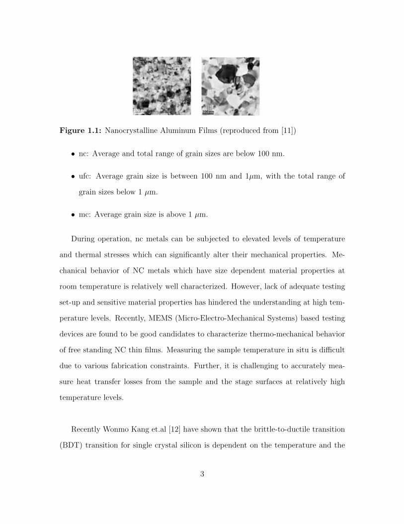
Figure 1.1: Nanocrystalline Aluminum Films (reproduced from [11])
• nc: Average and total range of grain sizes are below 100 nm.
• ufc: Average grain size is between 100 nm and 1µm, with the total range of
grain sizes below 1 µm.
• mc: Average grain size is above 1 µm.
During operation, nc metals can be subjected to elevated levels of temperature
and thermal stresses which can significantly alter their mechanical properties. Me-
chanical behavior of NC metals which have size dependent material properties at
room temperature is relatively well characterized. However, lack of adequate testing
set-up and sensitive material properties has hindered the understanding at high tem-
perature levels. Recently, MEMS (Micro-Electro-Mechanical Systems) based testing
devices are found to be good candidates to characterize thermo-mechanical behavior
of free standing NC thin films. Measuring the sample temperature in situ is difficult
due to various fabrication constraints. Further, it is challenging to accurately mea-
sure heat transfer losses from the sample and the stage surfaces at relatively high
temperature levels.
Recently Wonmo Kang et.al [12] have shown that the brittle-to-ductile transition
(BDT) transition for single crystal silicon is dependent on the temperature and the
3
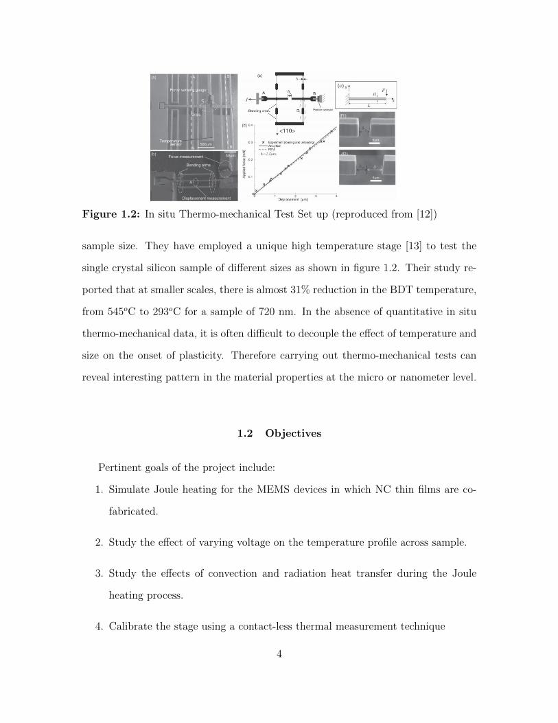
Figure 1.2: In situ Thermo-mechanical Test Set up (reproduced from [12])
sample size. They have employed a unique high temperature stage [13] to test the
single crystal silicon sample of different sizes as shown in figure 1.2. Their study re-
ported that at smaller scales, there is almost 31% reduction in the BDT temperature,
from 545oC to 293oC for a sample of 720 nm. In the absence of quantitative in situ
thermo-mechanical data, it is often difficult to decouple the effect of temperature and
size on the onset of plasticity. Therefore carrying out thermo-mechanical tests can
reveal interesting pattern in the material properties at the micro or nanometer level.
1.2 Objectives
Pertinent goals of the project include:
1. Simulate Joule heating for the MEMS devices in which NC thin films are co-
fabricated.
2. Study the effect of varying voltage on the temperature profile across sample.
3. Study the effects of convection and radiation heat transfer during the Joule
heating process.
4. Calibrate the stage using a contact-less thermal measurement technique
4

5. Carry out tensile test of titanium thin films at elevated temperature
1.3 Approach
To carry out the objectives stated above, it is beneficial to build a numerical model
which can predict the temperature profile of both the MEMS stage and the sample.
Finite Element Analysis (FEA) of the three dimensional solid model was carried out
using COMSOL Multiphysics package [14]. Some of the important features that ought
to be considered include that of meshing, appropriate physics package, boundary
conditions, radiative and convective effects, geometry effects and material properties.
Further, the calibration was carried out using thermoreflectance microscope which
can offer good spatial and temporal resolution.
1.4 Materials Under Study
The materials selected for the numerical model study are titanium and single
crystal silicon. Single crystal silicon is opted to verify the numerical model with
the previously carried out studies. For calibration and testing, MEMS based devices
with free standing Titanium thin films are taken up. Titanium has many applications
in the field of space and medicine. Titanium has a crystal class of hexagonal close
packing (hcp) and shows very little plasticity at room temperature under uniaxial
tension.
1.5 Structure of the Report
The first chapter gives a brief overview of Nanocrystalline metals and motivation
5

to take thermo-mechanical studies. Main objectives and the materials taken up for
study are also discussed in the same chapter.The second chapter explains the pro-
cess of simulating Joule heating of the stage and the samples.The next chapter talks
about calibration of the device using thermoreflectance microscope. The final chap-
ter provides important conclusions drawn from the study while discussing pertinent
limitations and outline for future work.
6

7
Chapter 2
NUMERICAL MODEL FOR JOULE HEATING
Numerical modeling has been carried out on the MEMS test stage in which the
nanocrystalline thin film is cofabricated. The results for titanium and Single Crystal
Silicon samples are provided in the current chapter. These results primarily include
voltage and temperature profile for the stage and the sample. Further, parametric
study has been carried out to study the effect of varying voltage on the temperature
profile of the sample.
2.1 Heat Transfer at the Micro/Nano Scale
The basic energy carriers in materials include mainly electrons, phonons and pho-
tons. In case of metals, electrons form the majority and dominate over other heat
carriers. Electrons in a metal are similar to that of atoms/molecules in a free gas hav-
ing a certain mean free path. The energy transport occurs through collisions which
are random in nature [15]. When the mean free path is comparable or larger than
the size of the system, quantum effects show pronounced effect. In this case, classical
heat transfer by Fourier heat conduction no longer applies and quantam mechanical
effects have to be taken into consideration. The general order for the mean free path
of the electrons is around 100 Ao. This is few orders lower than the size of our given
system (MEMS test stage as shown in figure 2.1) and nanoscale effects can essentially
be ignored [16]. However, in these micro devices the radiative and convective heat
losses/gain are enhanced as a result of the huge surface to volume ratio. Therefore it
is essential to consider these effects to accurately predict the temperature profile.
8
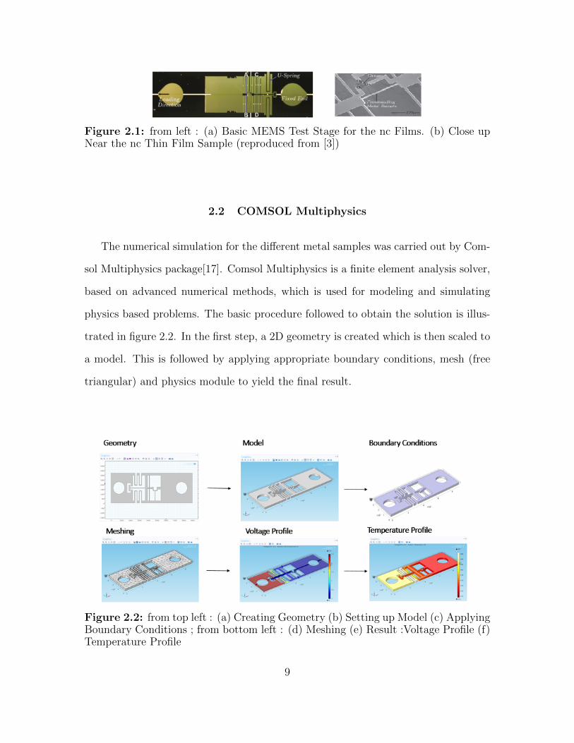
Figure 2.1: from left : (a) Basic MEMS Test Stage for the nc Films. (b) Close upNear the nc Thin Film Sample (reproduced from [3])
2.2 COMSOL Multiphysics
The numerical simulation for the different metal samples was carried out by Com-
sol Multiphysics package[17]. Comsol Multiphysics is a finite element analysis solver,
based on advanced numerical methods, which is used for modeling and simulating
physics based problems. The basic procedure followed to obtain the solution is illus-
trated in figure 2.2. In the first step, a 2D geometry is created which is then scaled to
a model. This is followed by applying appropriate boundary conditions, mesh (free
triangular) and physics module to yield the final result.
Figure 2.2: from top left : (a) Creating Geometry (b) Setting up Model (c) ApplyingBoundary Conditions ; from bottom left : (d) Meshing (e) Result :Voltage Profile (f)Temperature Profile
9
2.3 Mathematical Model
In order to simulate Joule heating Comsol couples the heat transfer in solids model
with the electric currents model. For heat transfer in solids the heat equation is given
by [18]
∂(ρcpT )
∂t= ∇ · (k∇T ) = div(k∇T ) +Qj(x, y, z, t) (2.1)
where ρ is the density, cp is the specific heat and Qj(x, y, z, t) is the Joule heating
term.k is some positive scalar quantity which may depend on the medium and is
called the thermal conductivity. The convection (with h: heat transfer coefficient,
T∞: Ambient temperature) and radiation (with σ′
: Stefan constant, ε: emissivity,
A: Area) boundary conditions applied in the current module are:
k∇T = h(T − T∞) + σ′εA(T 4 − T 4
∞) (2.2)
The sample is subjected to both a convective and radiative boundary condition at
the surface. The value Qj(x, y, z, t) depends upon the resistivity of the material, the
geometry of the structure and the current flowing through the device. Joule heating
involves the conversion of electrical energy to heat energy due to the resistance of the
element. This term is obtained with the help of the electric currents model in which
:
J = σE + Je (2.3)
E = −∇(V ) (2.4)
10

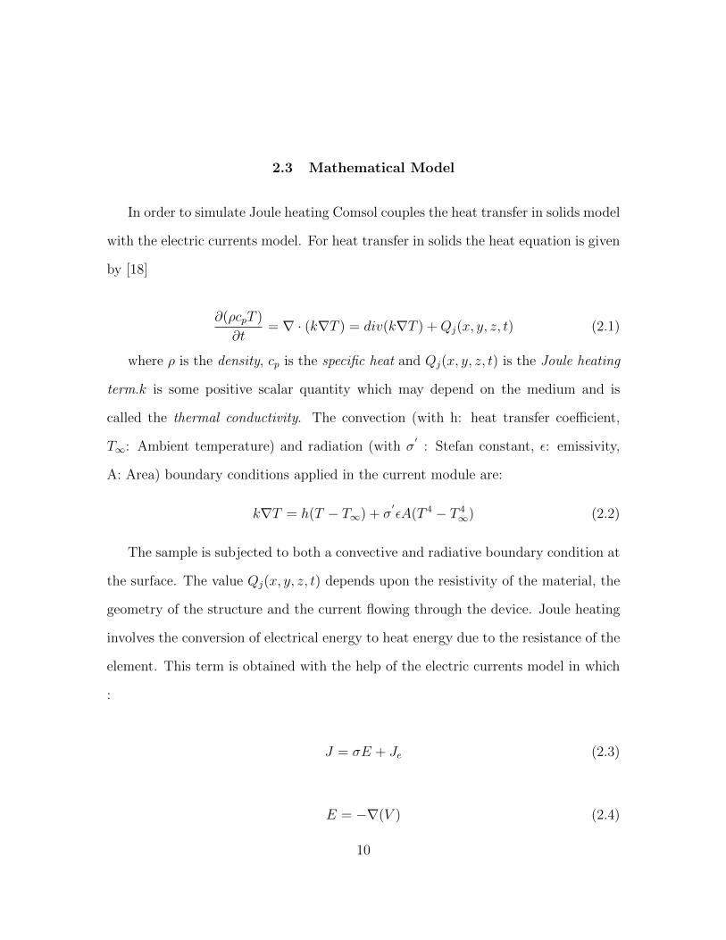
Figure 2.3: from left : (a) TEM Model (b) Ambient Model
Qj = ∇.(J) (2.5)
Where σ is the electrical conductivity, E the electric field, V the potential differ-
ence and J the current density. The above coupled equations would be trivial to solve
if there is homogeneous material with uniform current density and consistent material
properties.However, this is not the case in the current model where there are different
materials and properties that are temperature sensitive. The geometry was created in
Comsol based on the preexisting Autocad drawing. The model was created through
a series of Bezier Polygons in a work plane followed by an extrusion.Two different
geometries were considered : Ambient Model and TEM Model. Ambient model refers
to the one without backbeam and is meant for testing inside the lab as opposed to
a TEM model which has a back beam and is meant for study in situ in a TEM.The
figures for the Ambient and TEM model are shown in figure 2.3. The properties
for the materials were obtained from existing literature [19, 20] and care was taken
to select the most suitable values for our model. Most material properties such as
emissivity, heat capacity, thermal conductivity, and resistivity are a function of tem-
perature. Some of the properties can be entered as temperature dependent functions
in Comsol by making using of interpolation function. However, having the material
properties a function of temperature uses a lot of computing power while running the
11

simulation. The temperature dependence for all metal thin film samples was ignored.
For the silicon carbide sample the temperature dependence of resistivity was taken
into account since it varies significantly. The resistivity as a function of temperature
can be expressed using the linear relationship :
σ = σo(1 + (T − To)) (2.6)
where σ is the resistivity at temperature T, σo is the resistivity at temperatureTo.When
carrying out the experiment in an ambient environment we need to consider natural
convection. The convective heat transfer coefficient depends upon the temperature of
the film and the geometry. However we assumed a constant value for the convective
heat transfer coefficient of 5W/m2K. When carrying out the experiment in-situ we
can ignore heat transfer due to convection. The heat transfer due to radiation be-
comes then becomes dominant at elevated temperatures which can be evaluated using
by Stefan-Boltzmann law.A standard free triangular mesh was used for each surface
followed by a swept mesh. The use of a swept mesh is justified as the length of the
device is much larger than the thickness of the substrate and thin film . This reduces
our temperature distribution to two dimensions (namely the x and y).These simpli-
fications in the simulation may result in a certain level of inaccuracy in temperature
predictions. However, the trend followed during Joule heating follows a characteristic
parabolic rise.
2.4 Parametric Study
For device with titanium thin film, parametric study was carried out where the
voltage was varied from 0.1 V to 2.5 V. The temperature profile of the sample and the
stage was mapped taking into consideration radiation and convective heat transfer
12
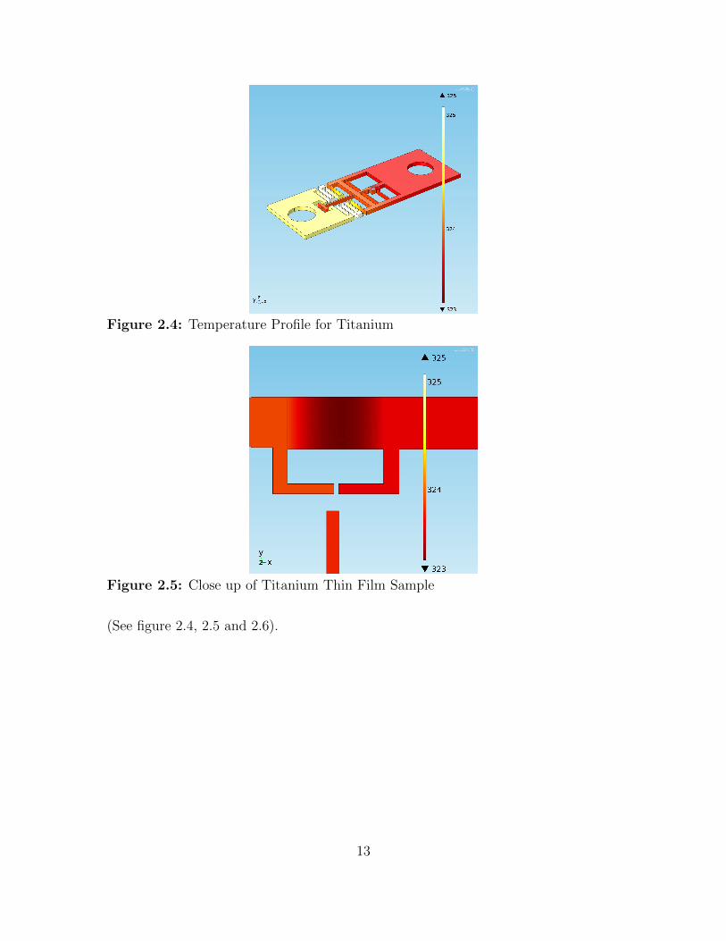
Figure 2.4: Temperature Profile for Titanium
Figure 2.5: Close up of Titanium Thin Film Sample
(See figure 2.4, 2.5 and 2.6).
13
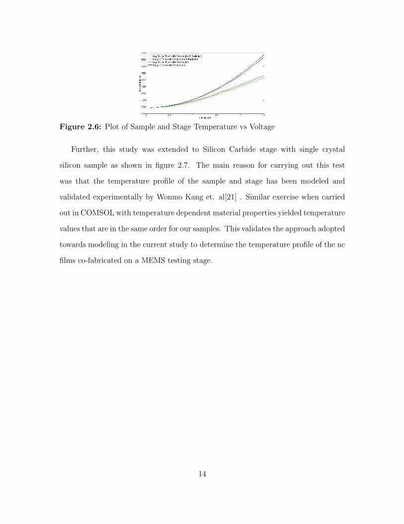
Figure 2.6: Plot of Sample and Stage Temperature vs Voltage
Further, this study was extended to Silicon Carbide stage with single crystal
silicon sample as shown in figure 2.7. The main reason for carrying out this test
was that the temperature profile of the sample and stage has been modeled and
validated experimentally by Wonmo Kang et. al[21] . Similar exercise when carried
out in COMSOL with temperature dependent material properties yielded temperature
values that are in the same order for our samples. This validates the approach adopted
towards modeling in the current study to determine the temperature profile of the nc
films co-fabricated on a MEMS testing stage.
14
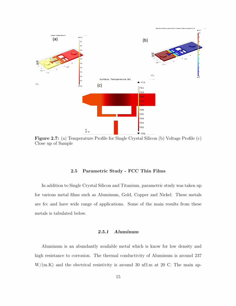
Figure 2.7: (a) Temperature Profile for Single Crystal Silicon (b) Voltage Profile (c)Close up of Sample
2.5 Parametric Study - FCC Thin Films
In addition to Single Crystal Silicon and Titanium, parametric study was taken up
for various metal films such as Aluminum, Gold, Copper and Nickel. These metals
are fcc and have wide range of applications. Some of the main results from these
metals is tabulated below.
2.5.1 Aluminum
Aluminum is an abundantly available metal which is know for low density and
high resistance to corrosion. The thermal conductivity of Aluminum is around 237
W/(m.K) and the electrical resistivity is around 30 nΩ.m at 20 C. The main ap-
15

Figure 2.8: Temperature Profile for Aluminum
plications are in transportation, packaging, construction etc. Parametric study was
carried out on free standing Aluminum thin films and the MEMS device as shown in
figure 2.8, 2.9 and 2.10.
16
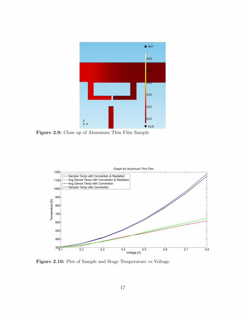
Figure 2.9: Close up of Aluminum Thin Film Sample
Figure 2.10: Plot of Sample and Stage Temperature vs Voltage
17

2.5.2 Copper
Copper is well know FCC metal with very high thermal and electrical conduc-
tivity. It is used both a building material and for electrical wirings. It has high
ductility with Young’s modulus varying from 110-128 GPa. The thermal conductiv-
ity of Copper is around 401 W/(m.K) and the electrical resistivity is around 17 nΩ.m
at 20 C.Parametric study was carried out on free standing Copper thin films and the
MEMS device as shown in figure 2.11, 2.12 and 2.13.
It can be observed that the temperature rise as a function of voltage is lower with
both convection and radiation effects considered. At higher temperature levels, the
difference is more significantly and cannot be ignored.
Figure 2.11: Temperature Profile for Copper
18

Figure 2.12: Close up of Copper Thin Film Sample
Figure 2.13: Plot of Sample and Stage Temperature vs Voltage
19

2.5.3 Nickel
Nickel is transition metal that is ductile and shows significant chemical activity
in the powdered state. At high temperature, Nickel is found to be ferromagnetic. It
has high Young’s modulus of around 200 GPa and is also anisotropic. The thermal
conductivity of Nickel is around 90.9 W/(m.K) and the electrical resistivity is around
69.3 nΩ.m at 20 C. Parametric study was carried out on free standing Nickel thin
films and the MEMS device as shown in 2.14, 2.15 and 2.16.
Nickel is currently being used in many applications including in making nickel
steels, nonferrous alloys and super alloys. It is in general an excellent alloying candi-
date for precious metals and bulk Nickel is found to be resistive to corrosion.
Figure 2.14: Temperature Profile for Nickel
20
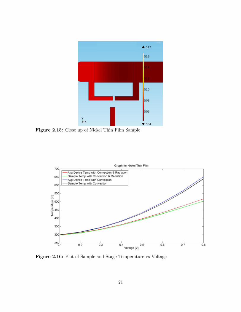
Figure 2.15: Close up of Nickel Thin Film Sample
Figure 2.16: Plot of Sample and Stage Temperature vs Voltage
21
2.5.4 Gold
Gold is a ductile metal and is a group 11 transition element. It is least reactive to
the chemicals and is to provide contacts in electronic packages. The Young’s modulus
is found to be around 79 GPa and is a good conductor of heat and electricity. The
thermal conductivity of Gold is around 318 W/(m.K) and the electrical resistivity is
around 22.14 nΩ.m at 20 C. Parametric study was carried out on free standing Gold
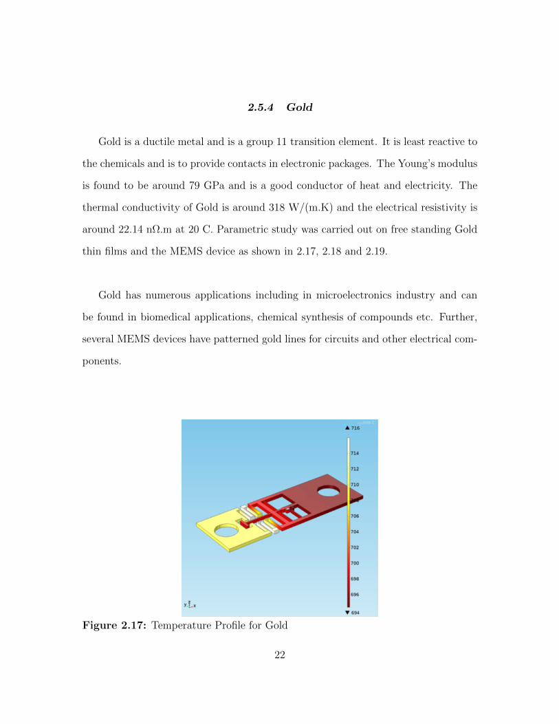
thin films and the MEMS device as shown in 2.17, 2.18 and 2.19.
Gold has numerous applications including in microelectronics industry and can
be found in biomedical applications, chemical synthesis of compounds etc. Further,
several MEMS devices have patterned gold lines for circuits and other electrical com-
ponents.
Figure 2.17: Temperature Profile for Gold
22

Figure 2.18: Close up of Gold Thin Film Sample
Figure 2.19: Plot of Sample and Stage Temperature vs Voltage
23

24
Chapter 3
CALIBRATION OF THE MEMS STAGE
3.1 Motivation
Measuring temperature accurately becomes non trivial when devices are scaled
down to the micro/nano scale [22]. Conventional techniques employing resistance
thermometer, thermocouple and thermistor often fail because of relatively larger size,
poor spatial and thermal resolution [23]. While contact techniques involving micro
thermocouples and mini thermistor sensors can be used to certain extent, they are
not suitable to measure temperature profile of features in the range of sub-micron
or nm range[24]. It is crucial to develop methods that can help in precise calibra-
tion and measurement of temperature profiles since they can have a strong impact
on device performance assessment and reliability. For example, space agencies of-
ten heavily use miniaturized devices to adhere to mass budget. The design of these
devices is often influenced by their thermal performance as per relevant MIL STD
regulations. It is therefore important to know what temperature distribution is across
the device during operation. Along with the above mentioned contact methods, there
are several contact-less techniques[25] such as IR (Infrared Thermography), near field
scanning optical microscopy (NSOM), scanning thermal microscopy (SThM), Raman
Measurements, thermoreflectance microscopy etc.[26, 27] that are being used for ther-
mal characterization of these devices. During Joule heating of the MEMS Stage, it is
important to know the temperature distribution across the device and the sample for
varying voltage. This helps in knowing the average temperature of the free standing
25

thin film being subjected to uniaxial tensile test. In particular, it is required to know
the general relationship interlinking the voltage and temperature for a set of devices
obtained from the same Silicon wafer. This ensures that calibration before each ten-
sile test is avoided by building a reliable model calibrated by input from experimental
measurements. To implement this goal, a scanning thermoreflectance microscope was
employed in this study.
3.2 Thermoreflectance Microscopy
Thermoreflectance microscope is a non-contact optical approach which relies on
change in reflectively for a given surface with change in temperature [28, 29] . This
technique offers high spatial and temporal resolution that can be very useful in pro-
ducing thermal maps of devices with resolved features being in the sub-micron regime.
The general set up of thermoreflectance microscope is shown in figure 3.1.
Figure 3.1: Schematic of Thermoreflectance Microscope (reproduced from [1])
26

The set up mainly comprises of laser source being focused on the sample after
passing through a 50:50 beam splitter with the reflected sample being captured by a
camera. In general the microscope arrangement consists of a laser diode driver, laser
diode controller, temperature controller and lock in amplifier. The goal is obtain a
reflected signal with a good signal to noise ratio. The simple form of the governing
equation [30, 31] is given below:
∆R
R=
1
R
∂R
∂T∆T = Ctr∆T (3.1)
In the above equation, ∆R is the change in reflectivity, T is the temperature
and Ctr is the thermoreflectance coefficient. This term depends strongly on the illu-
mination wavelength as seen in figure 3.2. From the figure, it can be seen that for
Titanium both Yellow (585 nm) and Red (660 nm) can be easily employed to measure
the sample temperature.
Figure 3.2: Variation of Thermoreflectance Coefficient with Illumination Wave-length (reproduced from [2])
27
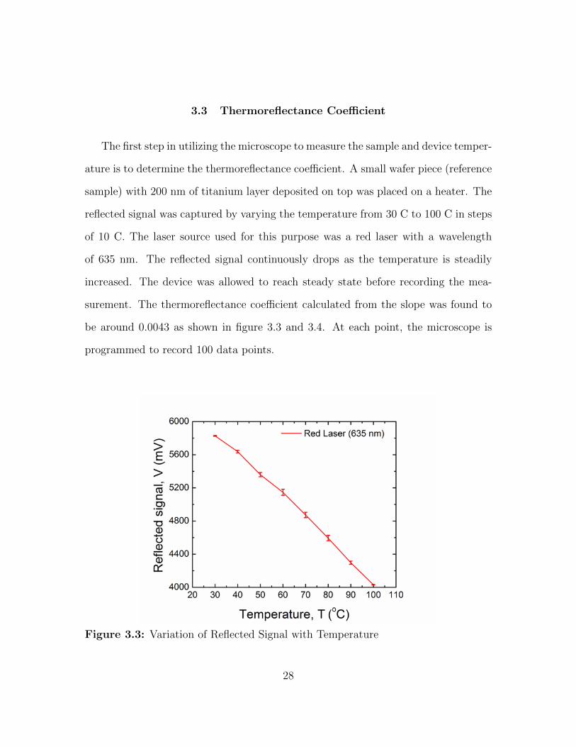
3.3 Thermoreflectance Coefficient
The first step in utilizing the microscope to measure the sample and device temper-
ature is to determine the thermoreflectance coefficient. A small wafer piece (reference
sample) with 200 nm of titanium layer deposited on top was placed on a heater. The
reflected signal was captured by varying the temperature from 30 C to 100 C in steps
of 10 C. The laser source used for this purpose was a red laser with a wavelength
of 635 nm. The reflected signal continuously drops as the temperature is steadily
increased. The device was allowed to reach steady state before recording the mea-
surement. The thermoreflectance coefficient calculated from the slope was found to
be around 0.0043 as shown in figure 3.3 and 3.4. At each point, the microscope is
programmed to record 100 data points.
Figure 3.3: Variation of Reflected Signal with Temperature
28
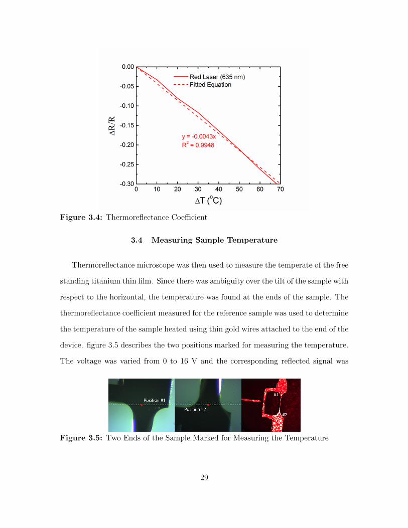
Figure 3.4: Thermoreflectance Coefficient
3.4 Measuring Sample Temperature
Thermoreflectance microscope was then used to measure the temperate of the free
standing titanium thin film. Since there was ambiguity over the tilt of the sample with
respect to the horizontal, the temperature was found at the ends of the sample. The
thermoreflectance coefficient measured for the reference sample was used to determine
the temperature of the sample heated using thin gold wires attached to the end of the
device. figure 3.5 describes the two positions marked for measuring the temperature.
The voltage was varied from 0 to 16 V and the corresponding reflected signal was
Figure 3.5: Two Ends of the Sample Marked for Measuring the Temperature
29

Figure 3.6: Reflected Signal Measurement
Figure 3.7: Temperature Measurements at Two Ends
30

Figure 3.8: Position 1: Laser Images
recorded for every 1V. The corresponding variation can be seen in figure 3.6 and 3.7.
Further, laser images were taken at both positions 1 and 2. It can clearly seen
than at lower voltages, the temperature induced due to Joule heating on the surface
is quite less. The incident laser is bright and thus there is good amount of normal
reflection and very little diffusion. With the increase in temperature, voltage signal
drops since there is high diffusion leading to very less normal reflection back to the
microscope. Thus, the shape of laser image thus becomes conformal to that of the
sample. This phenomenon is very clear in figure 3.8 and 3.9.
It is important to note that it is not possible to calibrate each sample that is
to be tested since calibration takes long time and it is quite tedious to move live
samples in between tensile stage and calibration stage. Using contacts such as silver
paste results in unique contact resistance that complicates the calibration process.
Therefore the idea is to employ a method such as wire bonding, which is discussed
in the next chapter to ensure uniform heating for all devices from the same parent
wafer.
31

Figure 3.9: Position 2: Laser Images
32

33

Chapter 4
EXPERIMENTAL TECHNIQUES
Experimentally realizing the high temperature tensile test is quite difficult. Num-
ber of significant challenges that crop up are making reliable contacts, measuring the
sample temperature accurately and preventing oxidation at higher temperature levels
etc. Further, this chapter also describes the process to fabricate the MEMS devices
and the micro structure characterization of the sputtered thin films.
4.1 Fabrication of the Device
The basic fabrication process flow used to fabricate the MEMS devices is show
in figure 4.1 . The device is designed to ensure uniaxial criterion during tensile test.
The basic steps involve:
• a) Deposition of the metal film on the wafer
• b) Spin coating of photo resist
• c) Removal of photo resist and etching silicon oxide layer
• d) photo resist deposition on both sides
• e) patterning both sides by lithography
• f) dry etching of the silicon oxide and removal of photo-resist
• g) DRIE etching of Si
• h) removal of oxide layer at the bottom of thin film
34
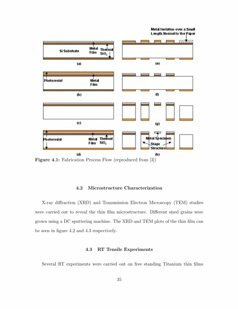
Figure 4.1: Fabrication Process Flow (reproduced from [3])
4.2 Microstructure Characterization
X-ray diffraction (XRD) and Transmission Electron Microscopy (TEM) studies
were carried out to reveal the thin film microstructure. Different sized grains were
grown using a DC sputtering machine. The XRD and TEM plots of the thin film can
be seen in figure 4.2 and 4.3 respectively.
4.3 RT Tensile Experiments
Several RT experiments were carried out on free standing Titanium thin films
35

Figure 4.2: TEM Image: Ti Thin Film Microstructure (Thickness: 200 nm at RT))
Figure 4.3: XRD Plots: Ti Thin Film (Thickness: 200 nm at RT)
36
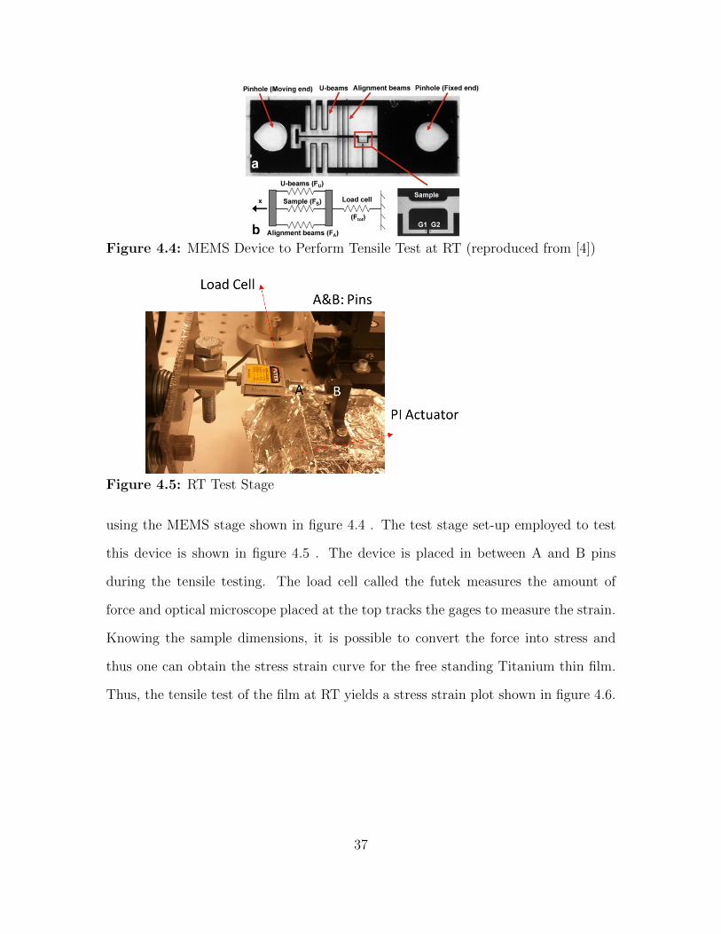
Figure 4.4: MEMS Device to Perform Tensile Test at RT (reproduced from [4])
Figure 4.5: RT Test Stage
using the MEMS stage shown in figure 4.4 . The test stage set-up employed to test
this device is shown in figure 4.5 . The device is placed in between A and B pins
during the tensile testing. The load cell called the futek measures the amount of
force and optical microscope placed at the top tracks the gages to measure the strain.
Knowing the sample dimensions, it is possible to convert the force into stress and
thus one can obtain the stress strain curve for the free standing Titanium thin film.
Thus, the tensile test of the film at RT yields a stress strain plot shown in figure 4.6.
37
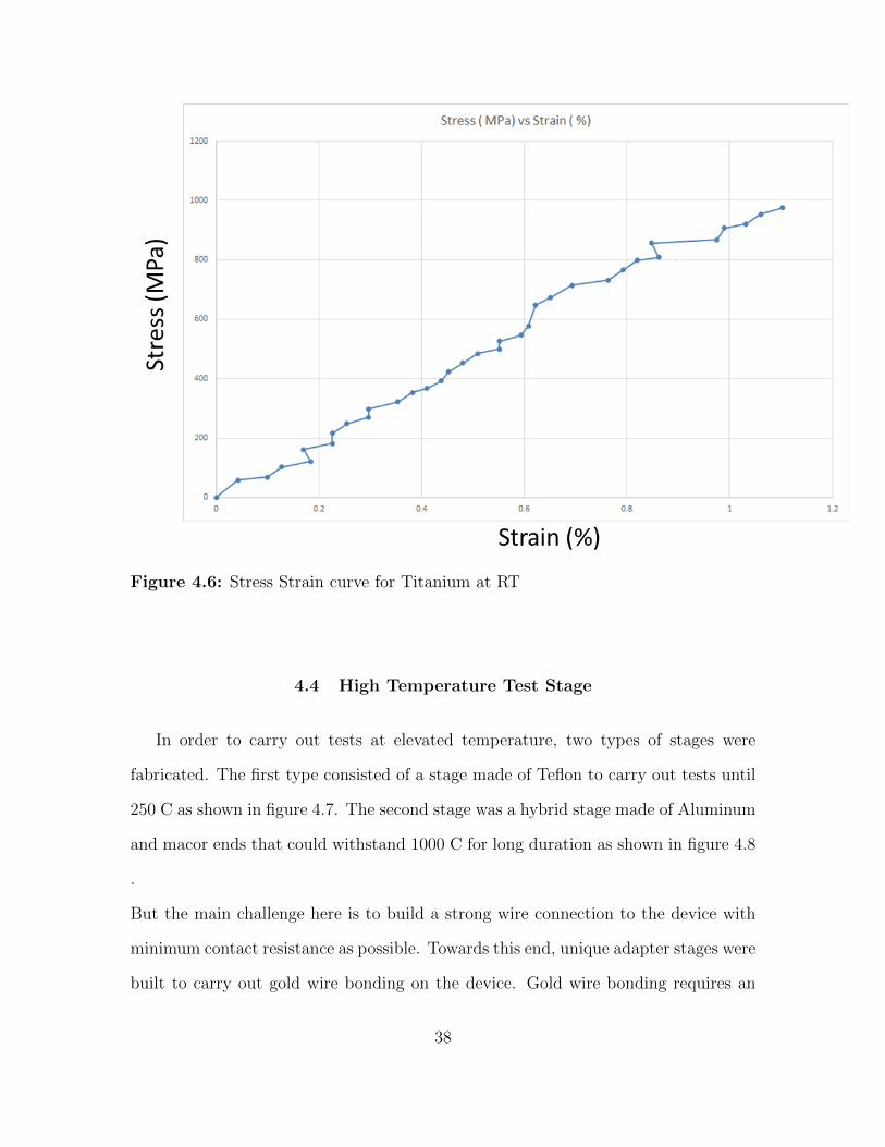
Figure 4.6: Stress Strain curve for Titanium at RT
4.4 High Temperature Test Stage
In order to carry out tests at elevated temperature, two types of stages were
fabricated. The first type consisted of a stage made of Teflon to carry out tests until
250 C as shown in figure 4.7. The second stage was a hybrid stage made of Aluminum
and macor ends that could withstand 1000 C for long duration as shown in figure 4.8
.
But the main challenge here is to build a strong wire connection to the device with
minimum contact resistance as possible. Towards this end, unique adapter stages were
built to carry out gold wire bonding on the device. Gold wire bonding requires an
38
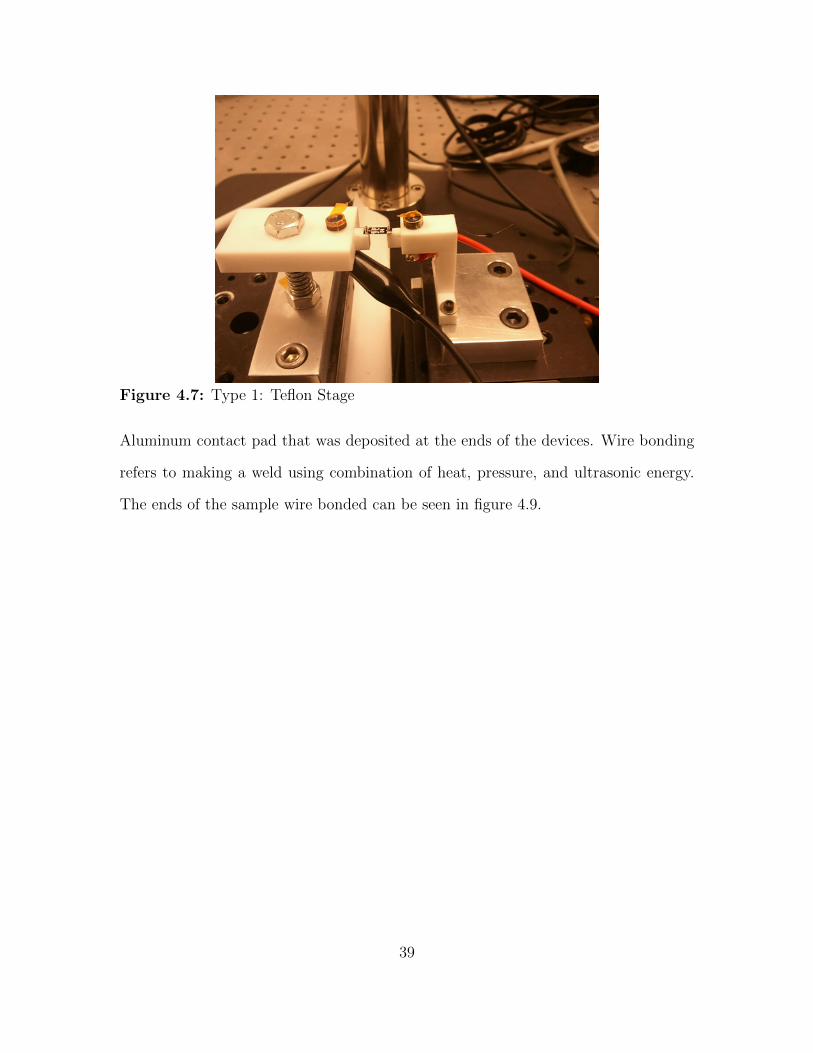
Figure 4.7: Type 1: Teflon Stage
Aluminum contact pad that was deposited at the ends of the devices. Wire bonding
refers to making a weld using combination of heat, pressure, and ultrasonic energy.
The ends of the sample wire bonded can be seen in figure 4.9.
39
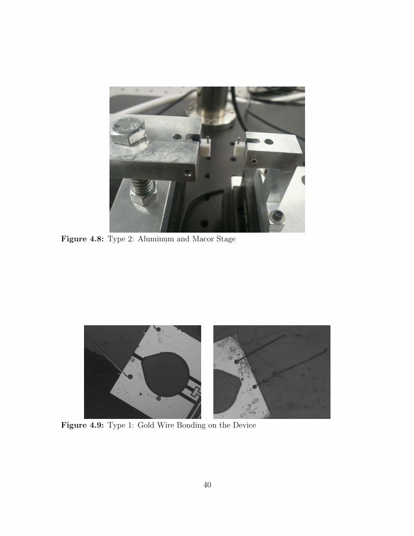
Figure 4.8: Type 2: Aluminum and Macor Stage
Figure 4.9: Type 1: Gold Wire Bonding on the Device
40

41

Chapter 5
CONCLUSION
The major objective of this study was to carry out modeling and calibration of
the MEMS Stage. Particularly, the goal was to determine the temperature profile of
the free standing nanocrystalline thin film sample co-fabricated with the MEMS test
stage. Towards this end numerical model involving Titanium with Silicon based stage
and Single Crystal Silicon(SCS) with Silicon Carbide was taken up. Further, calibra-
tion was carried out using thermoreflectance microscope on devices with titanium
thin films.
5.1 Conclusions
Some of the important conclusions that can be drawn from the study are :
1. Parametric modeling of the device and the sample has yielded a characteristic
temperature profile titanium and the Single Crystal Silicon(SCS) sample.The
temperature characteristic that is similar in all these cases is that of a parabolic
rise.
2. The temperature order and methodology followed to obtain Joule heating of the
MEMS stage is confirmed by the high temperature test on the Silicon Carbide
stage previously discussed in Wonmo Kang et.al
3. Titanium has very low conductivity and thus relatively high voltage is required
to heat up the sample compared to other metals.
42
4. Thermoreflectance microscope can be successfully employed to map the tem-
perature profile of the titanium sample
5.2 Limitations
There are some limitations in the numerical model that are worth mentioning.
These arise from the inability to account for all influence parameters at a single time
into the model. Some of the possible causes for the temperature offset are elucidated
below.
1. Meshing issues
(a) Difficulty in meshing small features
(b) Mesh misalignment
(c) Convergence issues
2. Material Properties
(a) Sensitive Material Properties
(b) Unavailability of data regarding temperature dependent properties
3. Oxide Thickness
(a) Thin layer of oxide layer may form at elevated temperature
(b) Incorporating such small layers into the model is difficult
4. Coupling Mechanical Behavior
(a) Coupling with multiple physics features leads very slow / no convergence
43

5.3 Outline for Further Work
The numerical model built for studying the Joule Heating can be improved with
adapting more factors influencing the temperature off set such as oxide layer thickness
etc. Further, tensile tests can be carried out at different temperatures for the titanium
sample to see the effect of temperature on plasticity.
44

REFERENCES
[1] Peter E. Raad Pavel L. Komarov Ali Shakouri Kazuaki Yazawa, Dustin Kendig.Understanding the thermoreflectance coefficient for high resolution thermal imag-ing of microelectronic devices. Electronics Cooling, 3(1):1, 2013.
[2] P.L. Komarov P. E. Raad and M. G. Burzo. Thermo-reflectance thermographyfor submicron temperature measurements. Electronics Cooling, 14(2):1, 2008.
[3] Jong H Han and M Taher A Saif. In situ microtensile stage for electrome-chanical characterization of nanoscale freestanding films. Review of ScientificInstruments, 77(4):045102, 2006.
[4] Ehsan Izadi and Jagannathan Rajagopalan. Texture dependent strain rate sen-sitivity of ultrafine-grained aluminum films. Scripta Materialia, 114:65–69, 2016.
[5] Jakob Schiøtz, Francesco D Di Tolla, and Karsten W Jacobsen. Softening ofnanocrystalline metals at very small grain sizes. Nature, 391(6667):561–563,1998.
[6] KS Kumar, H Van Swygenhoven, and S Suresh. Mechanical behavior of nanocrys-talline metals and alloys. Acta Materialia, 51(19):5743–5774, 2003.
[7] Ke Lu. Nanocrystalline metals crystallized from amorphous solids: nanocrys-tallization, structure, and properties. Materials Science and Engineering: R:Reports, 16(4):161–221, 1996.
[8] H Van Swygenhoven, PM Derlet, and AG Frøseth. Stacking fault energies andslip in nanocrystalline metals. Nature materials, 3(6):399–403, 2004.
[9] CC Koch. Optimization of strength and ductility in nanocrystalline and ultrafinegrained metals. Scripta Materialia, 49(7):657–662, 2003.
[10] V Yamakov, D Wolf, SR Phillpot, AK Mukherjee, and H Gleiter. Deformation-mechanism map for nanocrystalline metals by molecular-dynamics simulation.nature materials, 3(1):43–47, 2004.
[11] Jagannathan Rajagopalan, Jong H Han, and M Taher A Saif. Plastic deformationrecovery in freestanding nanocrystalline aluminum and gold thin films. Science,315(5820):1831–1834, 2007.
[12] Wonmo Kang and M Taher A Saif. In situ study of size and temperature depen-dent brittle-to-ductile transition in single crystal silicon. Advanced FunctionalMaterials, 23(6):713–719, 2013.
[13] Wonmo Kang and M Taher A Saif. A novel sic mems apparatus for in situ uniaxialtesting of micro/nanomaterials at high temperature. Journal of Micromechanicsand Microengineering, 21(10):105017, 2011.
45
[14] William BJ Zimmerman. Multiphysics Modeling With Finite Element Methods(series on Stability, vibration and control of systems, serie). World ScientificPublishing Co., Inc., 2006.
[15] PJ Price. Two-dimensional electron transport in semiconductor layers. i. phononscattering. Annals of Physics, 133(2):217–239, 1981.
[16] Dragica Vasileska and Stephen M Goodnick. Nano-Electronic Devices: Semi-classical and Quantum Transport Modeling. Springer Science & Business Media,2011.
[17] Comsol. COMSOL Multiphysics: Version 3.3. Comsol, 2006.
[18] Christie J Geankoplis. Transport processes and separation process principles.Prentice Hall Professional Technical Reference, 2003.
[19] RR Boyer. An overview on the use of titanium in the aerospace industry. Mate-rials Science and Engineering: A, 213(1):103–114, 1996.
[20] Yi Cui, Lincoln J Lauhon, Mark S Gudiksen, Jianfang Wang, and Charles MLieber. Diameter-controlled synthesis of single-crystal silicon nanowires. AppliedPhysics Letters, 78(15):2214–2216, 2001.
[21] Wonmo Kang and M Taher A Saif. In situ study of size and temperature depen-dent brittle-to-ductile transition in single crystal silicon. Advanced FunctionalMaterials, 23(6):713–719, 2013.
[22] M Farzaneh, K Maize, D Luerßen, JA Summers, PM Mayer, PE Raad, KP Pipe,A Shakouri, RJ Ram, and Janice A Hudgings. Ccd-based thermoreflectancemicroscopy: principles and applications. Journal of Physics D: Applied Physics,42(14):143001, 2009.
[23] Bincheng Li, L Pottier, JP Roger, D Fournier, K Watari, and K Hirao. Measuringthe anisotropic thermal diffusivity of silicon nitride grains by thermoreflectancemicroscopy. Journal of the european ceramic society, 19(8):1631–1639, 1999.
[24] Bincheng Li, L Pottier, JP Roger, and D Fournier. Thermal characterizationof thin superconducting films by modulated thermoreflectance microscopy. ThinSolid Films, 352(1):91–96, 1999.
[25] Stefan Dilhaire, Stephane Grauby, Wilfrid Claeys, and Jean-Christophe Batsale.Thermal parameters identification of micrometric layers of microelectronic de-vices by thermoreflectance microscopy. Microelectronics journal, 35(10):811–816,2004.
[26] G Tessier, G Jerosolimski, S Hole, D Fournier, and C Filloy. Measuring andpredicting the thermoreflectance sensitivity as a function of wavelength on en-capsulated materials. Review of Scientific Instruments, 74(1):495–499, 2003.
46

[27] Dietrich Luerßen, Janice A Hudgings, Peter M Mayer, and Rajeev J Ram.Nanoscale thermoreflectance with 10mk temperature resolution using stochasticresonance. In Semiconductor Thermal Measurement and Management Sympo-sium, 2005 IEEE Twenty First Annual IEEE, pages 253–258. IEEE, 2005.
[28] Stefan Dilhaire, Stephane Grauby, Sebastien Jorez, Luis-David Patino Lopez,Emmanuel Schaub, and Wilfrid Claeys. Laser diode cofd analysis by thermore-flectance microscopy. Microelectronics Reliability, 41(9):1597–1601, 2001.
[29] M Farzaneh, Reja Amatya, D Luerszen, Kathryn J Greenberg, Whitney E Rock-well, and Janice A Hudgings. Temperature profiling of vcsels by thermore-flectance microscopy. Photonics Technology Letters, IEEE, 19(8):601–603, 2007.
[30] LR De Freitas, EC Da Silva, AM Mansanares, G Tessier, and D Fournier. Sen-sitivity enhancement in thermoreflectance microscopy of semiconductor devicesusing suitable probe wavelengths. Journal of applied physics, 98(6):063508, 2005.
[31] J Christofferson, K Maize, Y Ezzahri, J Shabani, X Wang, and A Shakouri. Mi-croscale and nanoscale thermal characterization techniques. Journal of ElectronicPackaging, 130(4):041101, 2008.
47