Mobility Modeling in Advanced MOSFETs with Ultra-Thin Silicon Body
6
55 Journal Integrated Circuits and Systems 2009; v.4 / n.2:55-60 Mobility Modeling in Advanced MOSFETs with Ultra-Thin Silicon Body under Stress Viktor A. Sverdlov 1 , Thomas Windbacher 1 , Franz Schanovsky 2 , and Siegfried Selberherr 1 1 Institute for Microelectronics 2 Christian Doppler Laboratory for TCAD at the Institute for Microelectronics TU Wien, Gußhausstraße 27-29/E-360, A-1040 Wien, Austria e-mail: {Sverdlov|Windbacher|Schanovsky|Selberherr}@iue.tuwien.ac.at 1. INTRODUCTION The rapid increase in computational power and speed of integrated circuits is supported by the aggres- sive size reduction of semiconductor devices. Downscaling of MOSFETs as institutionalized by Moore’s law is successfully continuing because of innovative changes in the technological processes and the introduction of new materials. The 32nm MOS- FET process technology recently developed by Intel [1] involves new hafnium-based high-k dielectric/ metal gates and represents a major change in the tech- nological process since the invention of MOSFETs. Although alternative channel materials with a mobili- ty higher than in Si were already investigated [2, 3], it is believed that strained Si will be the main channel material for MOSFETs beyond the 45nm technology node [3]. With scaling apparently approaching its funda- mental limits, the semiconductor industry is facing crit- ical challenges. New engineering solutions and innova- tive techniques are required to improve CMOS device performance. Strain-induced mobility enhancement is the most attractive solution to increase the device speed and will certainly take a key position among other tech- nological changes for the next technology generations. In addition, new device architectures based on multi- gate structures with better electrostatic channel control and reduced short channel effects will be developed. A multi-gate MOSFET architecture is expected to be introduced for the 22nm technology node. Combined with a high-k dielectric/metal gate technology and strain engineering, a multi-gate MOSFET appears to be the ultimate device for high-speed operation with excel- lent channel control, reduced leakage currents, and low power budget. Confining carriers within thin Si films reduces the channel dimension in transversal direction, which further improves gate channel control. The quan- tization energy in ultra-thin Si films may reach a (few) hundred(s) meV. The parabolic band approximation usually employed for subband structure calculations of confined electrons in Si inversion layers becomes insuffi- cient in ultra-thin Si films. A recent study of subband energies and transport in (001) and (110) oriented thin Si films reveals that even the non-parabolic isotropic dis- persion is not sufficient to describe experimental data, and a direction-dependent anisotropic non-parabolicity must be introduced [4]. A comprehensive analysis of transport in multi- gate MOSFETs under general stress conditions is ABSTRACT1 We use a two-band k·p model to describe the subband structure in strained silicon thin films. The model provides the dependence of the conductivity effective mass on strain and film thickness. The conductivity mass decreases along tensile stress in [110] direction applied to a (001) film. This con- ductivity mass decrease ensures the mobility enhancement in MOSFETs even with extremely thin silicon films. The two-band k·p model also describes the dependence of the non-parabolicity param- eter on film thickness and strain. The influence of the subband structure modification on the mobili- ty in advanced MOSFETs with strained ultra-thin silicon body is investigated. It is shown that an increase of subband non-parabolicity in thin films with strain reduces the mobility enhancement due to the conductivity mass modification, especially at higher strain values. Index Terms: mobility enhancement, strained silicon, stress dependent conductivity mass, non-par- abolicity parameter, Monte Carlo simulation. 02-Sverdlov v4 n1-af 20.08.09 12:03 Page 55
Transcript of Mobility Modeling in Advanced MOSFETs with Ultra-Thin Silicon Body
55Journal Integrated Circuits and Systems 2009; v.4 / n.2:55-60
Mobility Modeling in Advanced MOSFETs with Ultra-Thin Silicon Body under Stress
Viktor A. Sverdlov1, Thomas Windbacher1, Franz Schanovsky2, and Siegfried Selberherr1
1Institute for Microelectronics 2Christian Doppler Laboratory for TCAD at the Institute for Microelectronics
TU Wien, Gußhausstraße 27-29/E-360, A-1040 Wien, Austria
e-mail: {Sverdlov|Windbacher|Schanovsky|Selberherr}@iue.tuwien.ac.at
1. INTRODUCTION
The rapid increase in computational power andspeed of integrated circuits is supported by the aggres-sive size reduction of semiconductor devices.Downscaling of MOSFETs as institutionalized byMoore’s law is successfully continuing because ofinnovative changes in the technological processes andthe introduction of new materials. The 32nm MOS-FET process technology recently developed by Intel[1] involves new hafnium-based high-k dielectric/metal gates and represents a major change in the tech-nological process since the invention of MOSFETs.Although alternative channel materials with a mobili-ty higher than in Si were already investigated [2, 3], itis believed that strained Si will be the main channelmaterial for MOSFETs beyond the 45nm technologynode [3].
With scaling apparently approaching its funda-mental limits, the semiconductor industry is facing crit-ical challenges. New engineering solutions and innova-tive techniques are required to improve CMOS deviceperformance. Strain-induced mobility enhancement isthe most attractive solution to increase the device speedand will certainly take a key position among other tech-
nological changes for the next technology generations.In addition, new device architectures based on multi-gate structures with better electrostatic channel controland reduced short channel effects will be developed. Amulti-gate MOSFET architecture is expected to beintroduced for the 22nm technology node. Combinedwith a high-k dielectric/metal gate technology andstrain engineering, a multi-gate MOSFET appears to bethe ultimate device for high-speed operation with excel-lent channel control, reduced leakage currents, and lowpower budget. Confining carriers within thin Si filmsreduces the channel dimension in transversal direction,which further improves gate channel control. The quan-tization energy in ultra-thin Si films may reach a (few)hundred(s) meV. The parabolic band approximationusually employed for subband structure calculations ofconfined electrons in Si inversion layers becomes insuffi-cient in ultra-thin Si films. A recent study of subbandenergies and transport in (001) and (110) oriented thinSi films reveals that even the non-parabolic isotropic dis-persion is not sufficient to describe experimental data,and a direction-dependent anisotropic non-parabolicitymust be introduced [4].
A comprehensive analysis of transport in multi-gate MOSFETs under general stress conditions is
ABSTRACT1
We use a two-band k·p model to describe the subband structure in strained silicon thin films. Themodel provides the dependence of the conductivity effective mass on strain and film thickness. Theconductivity mass decreases along tensile stress in [110] direction applied to a (001) film. This con-ductivity mass decrease ensures the mobility enhancement in MOSFETs even with extremely thinsilicon films. The two-band k·p model also describes the dependence of the non-parabolicity param-eter on film thickness and strain. The influence of the subband structure modification on the mobili-ty in advanced MOSFETs with strained ultra-thin silicon body is investigated. It is shown that anincrease of subband non-parabolicity in thin films with strain reduces the mobility enhancement dueto the conductivity mass modification, especially at higher strain values.
Index Terms: mobility enhancement, strained silicon, stress dependent conductivity mass, non-par-abolicity parameter, Monte Carlo simulation.
02-Sverdlov v4 n1-af 20.08.09 12:03 Page 55
Mobility Modeling in Advanced MOSFETs with Ultra-Thin Silicon Body under StressSverdlov, Windbacher, Schanovsky, & Selberherr
56 Journal Integrated Circuits and Systems 2009; v.4 / n.2:55-60
required for understanding the enhancement of deviceperformance. Besides the biaxial stress obtained byepitaxially growing silicon on a SiGe substrate, mo-dern techniques allow the generation of large uniaxialstress along the [110] channel. Stress in this directioninduces significant shear lattice distortion. The influ-ence of the shear distortion on subband structure andlow-field mobility has not yet been carefully analyzed.
The two-band k·p model [5-8] provides a gen-eral approach to compute the subband structure, inparticular the dependence of the electron effectivemasses on shear strain. In case of a square potentialwell with infinite walls, which is a good approximationfor the confining potential in ultra-thin Si films, thesubband structure can be obtained analytically [9].This allows an analysis of subband energies, effectivemasses, non-parabolicity and the low-field mobility onfilm thickness for arbitrary stress conditions.
In the following we briefly review the main ideasbehind the two-band k·p model for a valley in the con-duction band of Si. Then we shortly analyze theunprimed subband structure in (001) ultra-thin Si films,obtaining analytical dependences for the effective mass-es and non-parabolicity parameter. With these parame-ters the non-parabolic subband approximation for thesubband dispersions is constructed. The non-parabolicsubband dispersions is embedded into the subbandMonte Carlo code in order to enable the computationof the low-filed mobility. Results of the mobilityenhancement calculations are finally analyzed.
2.CONDUCTION BAND IN SILICON
The subband structure in a confined systemmust be based on accurate bulk bands of Si includingstrain. Several options are available. The conductionband dispersions computed with several methods in[100] and [110] directions are compared in Fig.1.The method based on non-local empirical pseudo-potentials from [10] is the most accurate as comparedto DFT band structure results obtained with VASP[11]. The sp3d5s* tight-binding model with parame-ters from [12] does not reproduce the anisotropy ofthe conduction band correctly. In addition, an accu-rate calibration of the parameters of the sp3d5s* modelto describe the modification of the conduction bandin strained Si is still lacking.
The k·p theory is a well established method todescribe the band structure analytically. As illustratedin Fig.1, the k·p method reproduces the band struc-ture accurately at energies below 0.5eV, which isenough to describe the subband structure and trans-port properties of advanced MOSFETs. From symme-try consideration the two-band k·p Hamiltonian of a[001] valley in the vicinity of the X point of theBrillouin zone in Si must be in the form [6]:
where σy,z are the Pauli matrices, I is the 2x2unity matrix, mt and ml are the transversal and the lon-gitudinal effective masses, k0 = 0.15 x 2π/a is the posi-tion of the valley minimum relative to the X point inunstrained Si, εxy denotes the shear strain component,M-1 ≈ m-1–m0
-1, and D=14eV is the shear strain defor-mation potential [5-8]. The two-band Hamiltonianresults in the following dispersions [6]:
where the negative sign corresponds to thelowest conduction band,
Ek
m
k k
m
k k
mz
l
x y
t
z
l
= ++
±
+
h h h2 2 2 2 2 20
2
2
2 2
( )δ
Hk
m
k k
mI D
k k
M
h k k
m
z
l
x yz
txy
x yz
z
ly
= ++
+ −
+
h h h2 2 2 2 2
20
2 2
( )ε σ
σ
(1)
(2)
Figure 1. Comparison of bulk dispersion relations close at theminimum of the [001] valleys of the conduction band in [100] and[110] directions. DFT [11] and EPM [7,10] results are similar whilethe sp3d5s* tight-binding model [12] underestimates anisotropysignificantly.
All moments as well as energies in (2) arecounted from the X-point of the Brillouin zone. Theclassical parabolic approximation is obtained from (2),when coupling between the two conduction bandsdescribed by the parameter is neglected. Couplingbetween the bands is small, when the wave vectors|kx|, |ky| << k0 (M/ml)1/2 and shear strain εxy = 0 . Dueto band coupling the dispersion (2) becomes non-par-abolic in strained Si, if the shear strain component isnon-zero, and/or at higher energies.
In order to check the accuracy of (2) we havecarried out numerical band structure calculations withthe empirical pseudo-potential method (EPM) withparameters from [7,10]. Excellent agreement betweenthe two-band k·p model (1) and the EPM results was
δ2 = Dεxy - h2kxky / M 2
2
(3)
02-Sverdlov v4 n1-af 20.08.09 12:03 Page 56
Mobility Modeling in Advanced MOSFETs with Ultra-Thin Silicon Body under StressSverdlov, Windbacher, Schanovsky, & Selberherr
57Journal Integrated Circuits and Systems 2009; v.4 / n.2:55-60
found up to energy 0.5eV. The relation (2) is valid ina larger range of energies compared to parabolic dis-persion with isotropic non-parabolic correction andcan be used to determine the subband structure inthin Si films.
3. SUBBAND EFFECTIVE MASSES
The subband energies can be found analyticallyfor an infinite square well potential which is a goodaproximation for an ultra-thin Si film. The dispersionof the unprimed subbands in a [001] thin Si film ofthickness t is [9]:
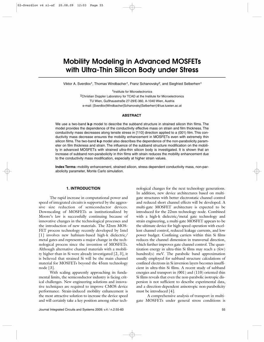
(6) is obtained after taking into account thestrain-induced valley minimum energy shift
and the dependence of thelongitudinal mass ml on strain [7, 8]:
Figure 2. Strain-modified subband effective mass (solid lines).Strain dependence of the transversal mass in bulk silicon isshown by dashed lines and symbols (results of pseudo-potentialcalculations).
where qn = (πn)/(tk0) and is the subband dispersionfor parabolic bands:
(4) is valid when
(5)
Dispersion (4) describes the subband quantiza-tion energy correction due to strain with respect tothe valley minimum:
∆
∆
En
m t
D m
k q
Eq
q
n xyl
xy l
n
xyn
n
( )( )
( )
( )( )
επ ε
ε
= −−
=−
2 2
2
2
204 2
2
2
2 1
1
h
12 2 2 2 4
04−( ) >q m kn lδ /h
E k k
n
m t
k k
m
k
mn x yl
x y
t l
02 2 2
2
2 2 2 202
2 2 2( , )
( )= +
+−
h h hπ
)]1(2/[),(),( 220
220nlyxnyxn qkmkkEkkE −−= hδ
(6)
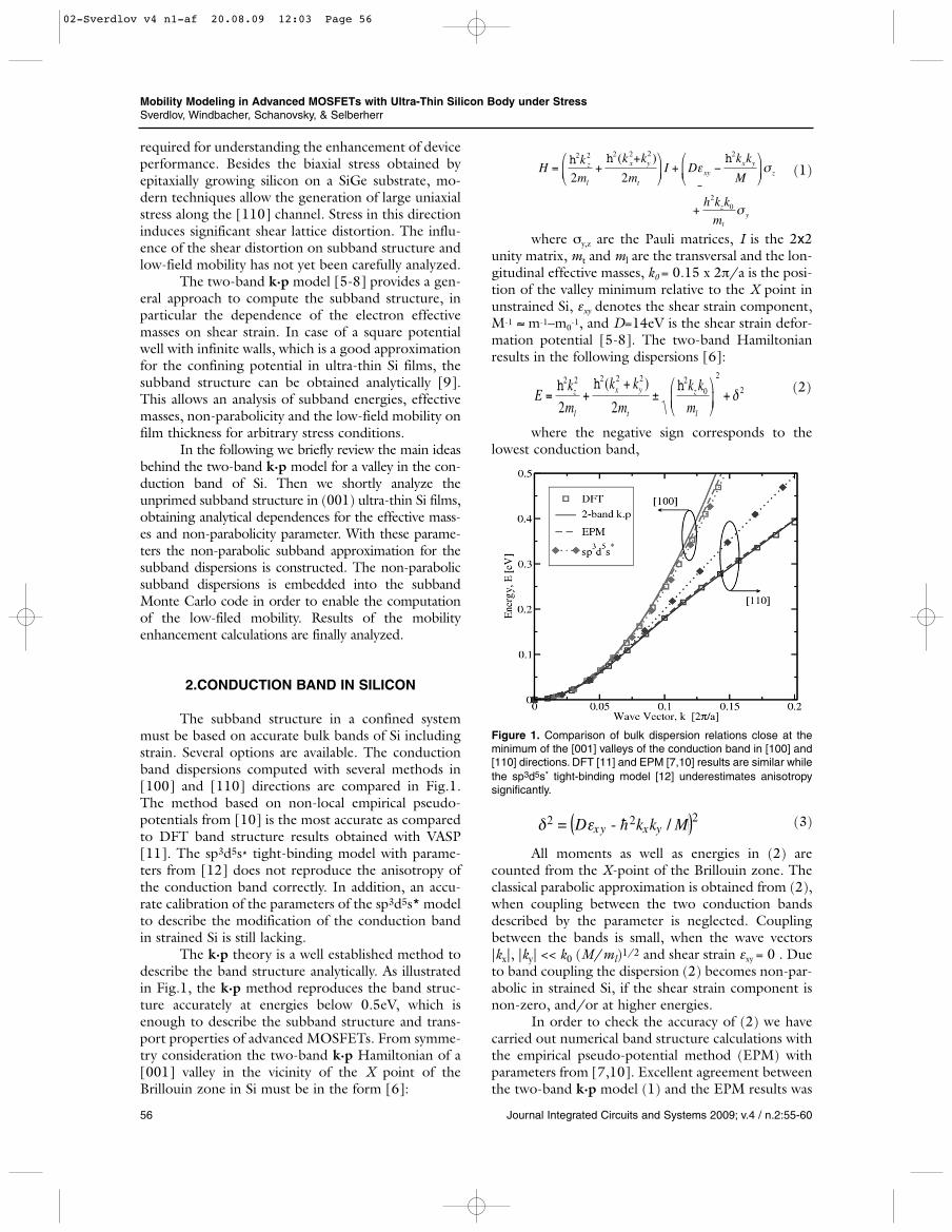
Figure 3. Subband dispersion (4) (solid) as compared to the pa-rabolic approximation (dotted), for a strained film (εxy = 1%) ofthickness t=5.4nm. Spacing between lines is 10meV.
(4) also describes corrections to the transversalmass mt due to strain εxy , to thickness t, and subbandnumber n:
Here mt- is the effective mass along the direc-
tion [110] of tensile stress. In thin films the effectivemass depends not only on strain but also on filmthickness. (7) is compared to the correspondingdependence in bulk silicon in Fig.2. The thicknessdependence of the last term in (7) leads to a morepronounced anisotropy in the transversal mass than ina bulk semiconductor.
A comparison of the dispersion relation (4) tothe para bolic approximation with transversal masses(7) for a strained film ( ) of thickness t=5.4nmis shown in Fig.3. Deviations from the parabolicapproximation become large for electron energiesabove 20meV. Therefore, to compute the carrier con-centration and mobility in thin Si films the dispersionrelation (4) should be used instead of a parabolicapproximation at higher carrier concentrations.
m m
D m
k
m
M qt txy l t
n
m
h= ±
−
−
11
1202 2
1ε
| |
mm
D m k
m
E k m
l xyl
xy l
l
xy l
( )( ) /
( ) /( / )
εε
ε
=−
=−
1
1 2
2 404
202
h
h
∆
(7)
∆E D m kxy xy l( ) ( ) /( )ε ε= − 2 2022h
ε xy = 1%
(4)
02-Sverdlov v4 n1-af 20.08.09 12:03 Page 57
Mobility Modeling in Advanced MOSFETs with Ultra-Thin Silicon Body under StressSverdlov, Windbacher, Schanovsky, & Selberherr
58 Journal Integrated Circuits and Systems 2009; v.4 / n.2:55-60
4. THE SUBBAND NON-PARABOLICITY
Taking into account the energy shift (6) and thesubband effective mass modifications (7) the subbanddispersion (4) close to the minimum is written as:
Substituting (11) into (10) and assuming theenergy E is close to the valley minimum so that ,we obtain the following expression for the non-parabo-licity parameter ratio:
The non-parabolicity parameter depends on thefilm thickness t via qn and strain η. We use (7) and(12) in order to evaluate the low-field mobility inFETs with ultra-thin Si films.
5. STRAIN INDUCED VALLEY SPLITTING
A weak coupling between the two valleys loca-ted at around the X-point leading to aso-called valley splitting [15] was neglected whileobtaining the subband dispersion relations (4). Thevalley splitting or, more precisely, the splittingbetween the two ladders of unprimed subbands reach-es several meVs in strongly confined electron systemsof Si point contacts [16]. We investigate for the firsttime how shear strain of arbitrary strength affects thevalley splitting.
For each energy E there are four solutions of(2) for the wave vectors ki (i=1,..,4). The wave func-tion is then a superposition of the solutions with thefour eigenvectors. In the two-bands model the wave
α η α
η
η
( , )tq
m
M q
m
M qn
t
n
t
n
=−
+−
−−
0 2
2
2
2
2
11
1 21
1
11
1
E
m
M k qm ml
n
= −−
−( )− +
ζϕ ϕ ζ
2 2
202 2
2 2 2 4
2 4 1h
( )cos sin
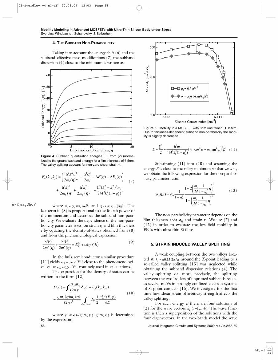
Figure 4. Subband quantization energies En from (2) (norma-lized to the ground subband energy) for a film thickness of 6.5nm.The valley splitting appears for non-zero shear strain η.
where and . Thelast term in (8) is proportional to the fourth power ofthe momentum and describes the subband non-para-bolicity. We evaluate the dependence of the non-para-bolicity parameter on strain η and film thicknesst by equating the density-of-states obtained from (8)and from the phenomenological expression
In the bulk semiconductor a similar procedure[11] yields e V-1 close to the phenomenologi-cal value eV-1 routinely used in calculations.
The expression for the density-of-states can bewritten in the form [12]
where is determinedby the expression:
D Edk dk
E E k k
m md
E
E
x yn x y
E const
( )( )
( ( , ))
( ) ( )
( )( , )
= −
=∂
∂
∫
∫− +
=
2
212
2
2
2
πδ
η η
πϕ
ζ ϕ
h h2 2 2 2
2 21
k
m
k
mE t E
t t
−−
−+
++ = +( )( ) ( )
( , )η η
α η
E k kn
m t
k
mE E
k
m
k
m
k k m
M k q
n x yl l
n
t t
l
n
( , )( )
( ) ( )
( ) ( )( )
( ),
= − − −
+ + −−
−−−
−+
+− +
h h
h h h
2 2 2
2
202
2 2 2 2 2 2 2 2
202 2
2 2
2 2 8 1
πη
η η
η η
∆ ∆
(8)
(9)
(10)
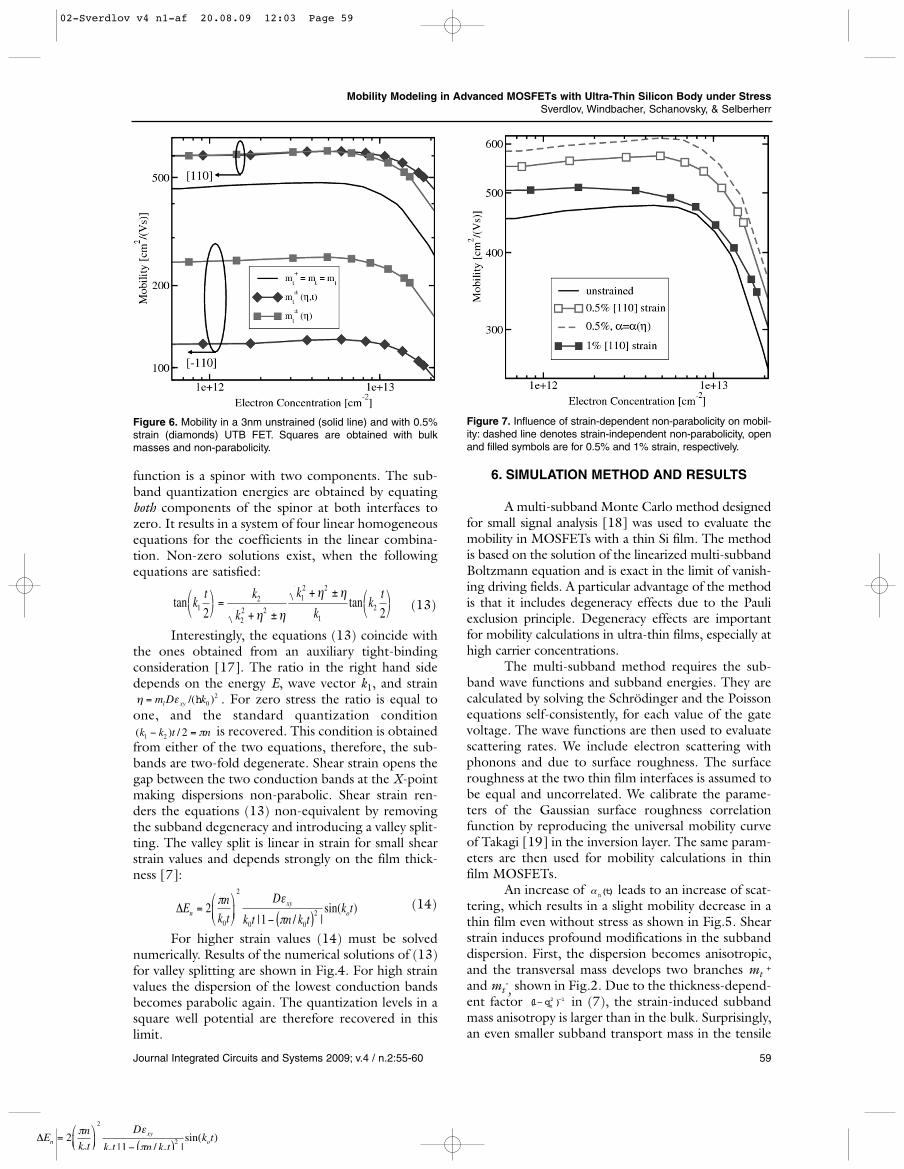
Figure 5. Mobility in a MOSFET with 3nm unstrained UTB film.Due to thickness-dependent subband non-parabolicity the mobi-lity is slightly decreased.
(11)
(12)
∆En
k tn =
2
0
π
2/)( yx kkk m=±
20)/( kDm xyl hεη =
),( tηα
α0 ≈ 0.6
α0 0 5= .
)(/)(/),( 222 ηηϕζ ++
−− += tt mkmkE
1<<Eα
k az = ±0 15 2. / π
η = Dml εxy / hk02
02-Sverdlov v4 n1-af 20.08.09 12:03 Page 58
Mobility Modeling in Advanced MOSFETs with Ultra-Thin Silicon Body under StressSverdlov, Windbacher, Schanovsky, & Selberherr
59Journal Integrated Circuits and Systems 2009; v.4 / n.2:55-60
function is a spinor with two components. The sub-band quantization energies are obtained by equatingboth components of the spinor at both interfaces tozero. It results in a system of four linear homogeneousequations for the coefficients in the linear combina-tion. Non-zero solutions exist, when the followingequations are satisfied:
Interestingly, the equations (13) coincide withthe ones obtained from an auxiliary tight-bindingconsideration [17]. The ratio in the right hand sidedepends on the energy E, wave vector k1, and strain
. For zero stress the ratio is equal toone, and the standard quantization condition
is recovered. This condition is obtainedfrom either of the two equations, therefore, the sub-bands are two-fold degenerate. Shear strain opens thegap between the two conduction bands at the X-pointmaking dispersions non-parabolic. Shear strain ren-ders the equations (13) non-equivalent by removingthe subband degeneracy and introducing a valley split-ting. The valley split is linear in strain for small shearstrain values and depends strongly on the film thick-ness [7]:
For higher strain values (14) must be solvednumerically. Results of the numerical solutions of (13)for valley splitting are shown in Fig.4. For high strainvalues the dispersion of the lowest conduction bandsbecomes parabolic again. The quantization levels in asquare well potential are therefore recovered in thislimit.
∆En
k t
D
k t n k tk tn
xyo=
− ( )2
10
2
0 0
2
π ε
π| / |sin( )
tan tankt k
k
k
kk
t1
2
22 2
12 2
122 2
=+ ±
+ ±
η η
η η
6. SIMULATION METHOD AND RESULTS
A multi-subband Monte Carlo method designedfor small signal analysis [18] was used to evaluate themobility in MOSFETs with a thin Si film. The methodis based on the solution of the linearized multi-subbandBoltzmann equation and is exact in the limit of vanish-ing driving fields. A particular advantage of the methodis that it includes degeneracy effects due to the Pauliexclusion principle. Degeneracy effects are importantfor mobility calculations in ultra-thin films, especially athigh carrier concentrations.
The multi-subband method requires the sub-band wave functions and subband energies. They arecalculated by solving the Schrödinger and the Poissonequations self-consistently, for each value of the gatevoltage. The wave functions are then used to evaluatescattering rates. We include electron scattering withphonons and due to surface roughness. The surfaceroughness at the two thin film interfaces is assumed tobe equal and uncorrelated. We calibrate the parame-ters of the Gaussian surface roughness correlationfunction by reproducing the universal mobility curveof Takagi [19] in the inversion layer. The same param-eters are then used for mobility calculations in thinfilm MOSFETs.
An increase of leads to an increase of scat-tering, which results in a slight mobility decrease in athin film even without stress as shown in Fig.5. Shearstrain induces profound modifications in the subbanddispersion. First, the dispersion becomes anisotropic,and the transversal mass develops two branches mt
+
and mt-, shown in Fig.2. Due to the thickness-depend-
ent factor in (7), the strain-induced subbandmass anisotropy is larger than in the bulk. Surprisingly,an even smaller subband transport mass in the tensile
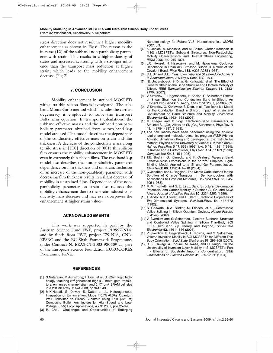
Figure 6. Mobility in a 3nm unstrained (solid line) and with 0.5%strain (diamonds) UTB FET. Squares are obtained with bulkmasses and non-parabolicity.
(13)
∆En
k t
D
k t n k tk tn
xyo=
− ( )2
10
2
0 0
2
π ε
π| / |sin( )
(14)
Figure 7. Influence of strain-dependent non-parabolicity on mobil-ity: dashed line denotes strain-independent non-parabolicity, openand filled symbols are for 0.5% and 1% strain, respectively.
η ε= m D kl xy /( )h 02
( ) /k k t n1 2 2− = π
)(tnα
12)1( −− nq
02-Sverdlov v4 n1-af 20.08.09 12:03 Page 59
Mobility Modeling in Advanced MOSFETs with Ultra-Thin Silicon Body under StressSverdlov, Windbacher, Schanovsky, & Selberherr
60 Journal Integrated Circuits and Systems 2009; v.4 / n.2:55-60
stress direction does not result in a higher mobilityenhancement as shown in Fig.6. The reason is theincrease (12) of the subband non-parabolicity param-eter with strain. This results in a higher density ofstates and increased scattering with a stronger influ-ence than the transport mass reduction at higherstrain, which leads to the mobility enhancementdecrease (Fig.7).
7. CONCLUSION
Mobility enhancement in strained MOSFETswith ultra-thin silicon films is investigated. The sub-band Monte Carlo method which includes the carriersdegeneracy is employed to solve the transportBoltzmann equation. In transport calculations, thesubband effective masses and the subband non-para-bolicity parameter obtained from a two-band k·pmodel are used. The model describes the dependenceof the conductivity effective mass on strain and filmthickness. A decrease of the conductivity mass alongtensile stress in [110] direction of (001) thin siliconfilm ensures the mobility enhancement in MOSFETseven in extremely thin silicon films. The two-band k·pmodel also describes the non-parabolicity parameterdependence on film thickness and on strain. Inclusionof an increase of the non-parablicity parameter withdecreasing film thickness results in a slight decrease ofmobility in unstrained films. Dependence of the non-parabolicity parameter on strain also reduces themobility enhancement due to the strain-induced con-ductivity mass decrease and may even overpower theenhancement at higher strain values.
ACKNOWLEDGEMENTS
This work was supported in part by theAustrian Science Fund FWF, project P19997-N14,and by funds from FWF, project I79-N16, CNR,EPSRC and the EC Sixth Framework Programme,under Contract N. ERAS-CT-2003-980409 as partof the European Science Foundation EUROCORESProgramme FoNE.
REFERENCES
[1] S.Natarajan, M.Armstrong, H.Bost, et al., A 32nm logic tech-nology featuring 2nd-generation high-k + metal-gate transis-tors, enhanced channel strain and 0.171µm2 SRAM cell sizein a 291Mb array, IEDM 2008, pp.941-943.
[2] M.K.Hudati, G. Dewey, S. Datta, et al., HeterogeneousIntegration of Enhancement Mode In0.7Ga0.3As QuantumWell Transistor on Silicon Substrate using Thin (<2 um)Composite Buffer Architecture for High-Speed and Low-Voltage (0.5V) Logic Applications, IEDM 2007, pp.625-628.
[3] R. Chau, Challenges and Opportunities of Emerging
Nanotechnology for Future VLSI Nanoelectronics, ISDRS2007, p.3.
[4] K. Uchida, A. Kinoshita, and M. Saitoh, Carrier Transport in(110) nMOSFETs: Subband Structures, Non-Parabolicity,Mobility Characteristics, and Uniaxial Stress Engineering,IEDM 2006, pp.1019-1021.
[5] J.C. Hensel, H. Hasegawa, and M. Nakayama, CyclotronResonance in Uniaxially Stressed Silicon. II. Nature of theCovalent Bond, Phys.Rev. 138, A225-A238 (1965).
[6] G.L.Bir and G.E. Pikus, Symmetry and Strain-Induced Effectsin Semiconductors, J.Willey & Sons, NY, 1974.
[7] E. Ungersboeck, S. Dhar, G. Karlowatz, et al., The Effect ofGeneral Strain on the Band Structure and Electron Mobility ofSilicon, IEEE Transactions on Electron Devices 54, 2183-2190, (2007).
[8] V. Sverdlov, E. Ungersboeck, H. Kosina, S. Selberherr, Effectsof Shear Strain on the Conduction Band in Silicon: AnEfficient Two-Band k.p Theory, ESSDERC 2007, pp.386-389.
[9] V. Sverdlov, G. Karlowatz, S. Dhar, et al., Two-Band k·p Modelfor the Conduction Band in Silicon: Impact of Strain andConfinement on Band Structure and Mobility, Solid-StateElectronics 52, 1563-1568 (2008).
[10]M. Rieger and P. Vogl, Electronic-Band Parameters inStrained Si1-xGex Alloys on Si1-yGey Substrates, Phys.Rev. B48, 14275-14287, (1993).
[11]The calculations have been performed using the ab-initiototal-energy and molecular-dynamics program VASP (ViennaAb-initio Simulation Program) developed at the Institute forMaterial Physics of the University of Vienna; G.Kresse and J.Hafner, Phys.Rev. B 47, 558 (1993); ibid. B 49, 14251 (1994);G.Kresse and J. Furthmueller, Phys.Rev. B 54, 11169 (1996);Computs.Mat.Sci. 6, 15 (1996).
[12]T.B. Boykin, G. Klimeck, and F. Oyafuso, Valence BandEffective-Mass Expressions in the sp3d5s* Empirical Tight-Binding Model Applied to a Si and Ge Parametrization,Phys.Rev.B 69, 115201-1—10 (2004).
[13]C. Jacoboni and L. Reggiani, The Monte Carlo Method for theSolution of Charge Transport in Semiconductors withApplications to Covalent Materials, Rev.Mod.Phys. 55, 645-705 (1983).
[14]M. V. Fischetti, and S. E. Laux, Band Structure, DeformationPotentials, and Carrier Mobility in Strained Si, Ge, and SiGeAlloys, Journal of Applied Physics 80, 2234-2252 (1996).
[15]T. Ando, A.B. Fowler, and F. Stern, Electronic Properties ofTwo-Dimensional Systems, Rev.Mod.Phys. 54, 437-672(1982).
[16]S. Goswami, K.A. Slinker, M. Friesen, et al., ControllableValley Splitting in Silicon Quantum Devices, Nature Physics3, 41-45 (2007).
[17]V. Sverdlov and S. Selberherr, Electron Subband Structureand Controlled Valley Splitting in Silicon Thin-Body SOIFETs: Two-Band k.p Theory and Beyond, Solid-StateElectronics 52, 1861-1866 (2008).
[18]V. Sverdlov, E. Ungersboeck, H. Kosina, and S. Selberherr,Volume Inversion Mobiliy in SOI MOSFETs for Different ThinBody Orientation, Solid State Electronics 51, 299-305 (2007).
[19] S. -I. Takagi, A. Toriumi, M. Iwase, and H. Tango, On theUniversality of Inversion Layer Mobility in Si MOSFETs: PartI - Effects of Substrate Impurity Concentration, IEEETransactions on Electron Devices 41, 2357-2362 (1994).
02-Sverdlov v4 n1-af 20.08.09 12:03 Page 60