
MKW01Z128 Package Information Ordering Information … · This document contains information on a...
67
© Freescale Semiconductor, Inc., 2014. All rights reserved. Freescale Semiconductor Advance Information This document contains information on a product under development. Freescale reserves the right to change or discontinue this product without notice. Document Number: MKW01Z128 Rev. 5, 3/2014 MKW01Z128 Package Information MKW01Z128 Ordering Information Device Device Marking Package MKW01Z128CHN MKW01Z128CHN LGA-60 1 Introduction The MKW01 device is highly-integrated, cost-effective, smart radio, sub-1 GHz wireless node solution composed of a transceiver supporting FSK, GFSK, MSK, or OOK modulations with a low-power ARM® Cortex M0+ CPU. The highly integrated RF transceiver operates over a wide frequency range including 315 MHz, 433 MHz, 470 MHz, 868 MHz, 915 MHz, 928 MHz, and 955 MHz in the license-free Industrial, Scientific and Medical (ISM) frequency bands. This configuration allows users to minimize the use of external components. The MKW01 is targeted for the following low-power wireless applications: • Automated Meter Reading • Wireless Sensor Networks • Home and Building Automation • Wireless Alarm and Security Systems • Industrial Monitoring and Control Freescale supplements the MKW01 with tools and software that include hardware evaluation and MKW01Z128 Highly-integrated, cost-effective single-package solution for sub-1 GHz applications 1 Introduction . . . . . . . . . . . . . . . . . . . . . . . . . . 1 2 Features . . . . . . . . . . . . . . . . . . . . . . . . . . . . . 2 3 Software Solutions . . . . . . . . . . . . . . . . . . . . . 5 4 Smart Radio Sub-1 GHz Wireless Node . . . . 5 5 MKW01 Pin Assignments and Connections 9 6 System and Power Management . . . . . . . . 15 7 Development Environment . . . . . . . . . . . . . 20 8 System Electrical Specification . . . . . . . . . 20 9 Typical Applications Circuit . . . . . . . . . . . . 25 10 Mechanical Drawings . . . . . . . . . . . . . . . . . 28
Transcript of MKW01Z128 Package Information Ordering Information … · This document contains information on a...

© Freescale Semiconductor, Inc., 2014. All rights reserved.
Freescale SemiconductorAdvance Information
This document contains information on a product under development. Freescale reserves the right to change or discontinue thisproduct without notice.
Document Number: MKW01Z128Rev. 5, 3/2014
MKW01Z128
Package Information
MKW01Z128
Ordering Information
Device Device Marking Package
MKW01Z128CHN MKW01Z128CHN LGA-60
1 IntroductionThe MKW01 device is highly-integrated, cost-effective, smart radio, sub-1 GHz wireless node solution composed of a transceiver supporting FSK, GFSK, MSK, or OOK modulations with a low-power ARM® Cortex M0+ CPU. The highly integrated RF transceiver operates over a wide frequency range including 315 MHz, 433 MHz, 470 MHz, 868 MHz, 915 MHz, 928 MHz, and 955 MHz in the license-free Industrial, Scientific and Medical (ISM) frequency bands. This configuration allows users to minimize the use of external components.
The MKW01 is targeted for the following low-power wireless applications:
• Automated Meter Reading
• Wireless Sensor Networks
• Home and Building Automation
• Wireless Alarm and Security Systems
• Industrial Monitoring and Control
Freescale supplements the MKW01 with tools and software that include hardware evaluation and
MKW01Z128Highly-integrated, cost-effective single-package solution for sub-1 GHz applications
1 Introduction . . . . . . . . . . . . . . . . . . . . . . . . . . 1
2 Features . . . . . . . . . . . . . . . . . . . . . . . . . . . . . 2
3 Software Solutions . . . . . . . . . . . . . . . . . . . . . 5
4 Smart Radio Sub-1 GHz Wireless Node . . . . 5
5 MKW01 Pin Assignments and Connections 9
6 System and Power Management . . . . . . . . 15
7 Development Environment . . . . . . . . . . . . . 20
8 System Electrical Specification . . . . . . . . . 20
9 Typical Applications Circuit . . . . . . . . . . . . 25
10 Mechanical Drawings . . . . . . . . . . . . . . . . . 28

MKW01Z128 Advance Information, Rev. 5
2 Freescale Semiconductor
development boards, software development IDE and applications, drivers, custom PHY usable with Freescale’s IEEE 802.15.4 compatible MAC and SMAC.
2 FeaturesThis section provides a simplified block diagram and highlights MKW01 features.
2.1 Block Diagram
Figure 1 shows a simplified block diagram of the MKW01.
Figure 1. MKW01 Simplified Block Diagram
2.2 Features Summary• RF Transceiver Features
— Operating Voltage from 1.8V to 3.6V.
— Programmable bit rate up to 600kbps (FSK)
— High Sensitivity: down to -120 dBm at 1.2 kbps
— High Selectivity: 16-tap FIR Channel Filter
Kinetis MKW01 Wireless MCU
Core
ARM Cortex-M0+48 MHz
DebugInterfaces
InterruptController
Analog
12-bit DAC
16-bit ADC
AnalogComparator
Six-ChannelTimer/PWM (TPM)
Periodic Interrupt
Timers
Low-PowerTimer
Real-Time Clock32-bit Timer
Timers
System
DMA
Low-LeakageWake-Up Unit
Memory
128 KB Flash
16 KB RAM
Interfaces
Sub-1 GHz Transceiver
2x I2C
3x UART
GPIOs
Touch Sensing
1x SPI
RF Transmitter and
32 MHz Oscillator
PLL
Packet Engine (AES)
66 ByteFIFO
Clocks
Phase-LockedLoop
Frequency-Locked Loop
Reference
Internal ReferenceClocks
Oscillators
Receiver
Synthesizer

MKW01Z128 Advance Information, Rev. 5
Freescale Semiconductor 3
— Bullet-proof front end: IIP3 = -18 dBm, IIP2 = +35 dBm, 80 dB Blocking Immunity, no Image Frequency response
— Low current: Rx = 16mA, 100nA register retention
— Programmable Pout : -18 to +17 dBm in 1 dB steps
— Constant RF performance over voltage range of chip
— Fully integrated synthesizer with a resolution of 61 Hz
— FSK, GFSK, MSK, GMSK and OOK modulations
— Built-in Bit Synchronizer performing Clock recovery
— Incoming Sync Word Recognition
— Automatic RF Sense with ultra-fast AFC
— Packet engine with CRC, AES-128 encryption and 66-byte FIFO
— Built-in temperature sensor and Low battery indicator
— 32 MHz crystal oscillator clock source
— Dedicated I/O’s for connection with an external 32 kHz crystal
• MCU Features
System:
— 48 MHz Max. Central Processor Unit (CPU) frequency
— 24 MHz Max. Bus frequency
— Vectored Interrupt Controller (NVIC) with 32 core-vectored interrupts with 4 programmable interrupt priority levels
— Asynchronous Wake-up Interrupt Controller (AWIC)
— 4 channel Direct Memory Access (DMA)
— DMA request multiplex
— Non Maskable Interrupt (NMI)
— COP Watchdog
— Low leakage Wake-up Unit (LLWU)
— Debug and Trace
– 2-pin Serial Wire Debug (SWD)
— 80-bit wide ID number
Memory:
— 128 KB P-Flash with 64 byte flash cache
— 16 KB RAM
Clocks:
— External crystal oscillator or resonator:
– 32 - 40 kHz low range, low power or full swing
– 3 MHz - 32 MHz high range, low power or full swing
— DC - 48 MHz external square wave input clock
MKW01Z128 Advance Information, Rev. 5
4 Freescale Semiconductor
— Internal clock references:
– 31.25 kHz to 39.063 kHz oscillator with +/– 1.5% max. deviation from 0 to +70C– 4 MHz oscillator with +/– 3% max. deviation across temperature
– 1 kHz oscillator
— Phase Locked Loop (PLL) with up to 100 MHz VCO
— Frequency Locked Loop (FLL):
– Low range: 20 - 25 MHz
– Mid range: 40 - 48 MHz
Analog:
— Power Management Controller (PMC) with low voltage warning (LVW) and detect with selectable trip points.
— 16-bit analog to digital converter
– 11 single ended channels available
– 2 status, control and results registers
– DMA support
— 1 High Speed Comparator (HSCMP) with internal 6-bit digital to analog converters (DAC)
— One 12-bit DAC with DMA support and 2 word data buffer
Timers:
— Six channel Timer/PWM (TPM)
— Periodic interrupt timers
— 16-bit low-power timer (LPTMR) can be configured to operate as a time counter or as a pulse counter, across all power modes, including the low-leakage modes
— Real-time clock 32-bit timer
Wired Communication Interface:
— One Serial Peripheral Interface (SPI) available externally
— Two Inter-Integrated Circuits (I2C) with DMA support
— Three Universal Asynchronous Receiver / Transmitter (UART) with DMA Support
– UART0 supports standard features plus:
• TxD pin can be configured as pseudo open drain for 1-wire half-duplex
• x4 to x32 oversampling
• Functional in VLPS mode
• LIN slave operation
– UART1 and UART2 support standard features
Human Machine Interface (HMI)
— General Purpose Input/Output (GPIO) supporting:

MKW01Z128 Advance Information, Rev. 5
Freescale Semiconductor 5
– Default to disabled (no leakage)
– 4 pins with 18 mA high current drive capability
– Hysteresis and configurable pull up device on all input pins
– Slew rate and drive strength fixed on all output pins
– Single cycle GPIO control via IOPORT
— Touch Sensor Inputs (TSI)
– 9-channel
– Selectable single channel wakeup source available in all modes
– DMA support
— Pin Interrupt
1.8 V to 3.6 V operating voltage with on-chip voltage regulators
Temperature range of –40C to 85C
60-pin LGA (8x8 mm) package
3 Software SolutionsFreescale will support the MKW01 platform with several software solutions:
• A radio utility GUI will be available that allows testing of various features and setting registers. A connectivity test firmware will allow a limited set of testing controlled with a terminal emulator on any computer.
• SMAC (Simple Media Access Controller) — This codebase provides simple communication and test apps based on drivers/PHY utilities available as source code. This environment is useful for hardware and RF debug, hardware standards certification, and developing proprietary applications.
• Additional software will be available through 3rd party providers.
4 Smart Radio Sub-1 GHz Wireless NodeThe MKW01 brings together a transceiver chip and an MCU chip on a single substrate to provide a small footprint, cost-effective sub-1 GHz wireless node. The transceiver is controlled by the MCU through a dedicated SPI interface. The SPI bus interface and some status signals are connected in-package the substrate to eliminate the need for external connections. The SPI supports bit order swapping providing hardware support for bit endianess reducing processing overhead.
4.1 RF Transceiver
The transceiver (see Figure 2) is a single-chip integrated circuit ideally suited for today's high performance ISM band RF applications. Its advanced features set, including state of the art packet engine, greatly simplifies system design while the high level of integration reduces the external RF component bill of material (BOM) to a handful of passive de-coupling and matching components. It is intended for use as a high-performance, low-cost FSK, GFSK, MSK, GMSK, and OOK RF transceiver for robust, frequency agile, half-duplex bi-directional RF links.
MKW01Z128 Advance Information, Rev. 5
6 Freescale Semiconductor
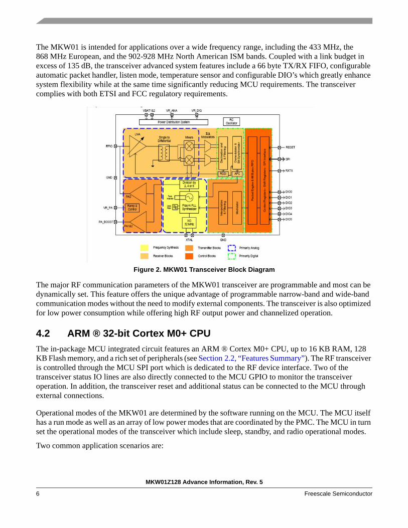
The MKW01 is intended for applications over a wide frequency range, including the 433 MHz, the 868 MHz European, and the 902-928 MHz North American ISM bands. Coupled with a link budget in excess of 135 dB, the transceiver advanced system features include a 66 byte TX/RX FIFO, configurable automatic packet handler, listen mode, temperature sensor and configurable DIO’s which greatly enhance system flexibility while at the same time significantly reducing MCU requirements. The transceiver complies with both ETSI and FCC regulatory requirements.
Figure 2. MKW01 Transceiver Block Diagram
The major RF communication parameters of the MKW01 transceiver are programmable and most can be dynamically set. This feature offers the unique advantage of programmable narrow-band and wide-band communication modes without the need to modify external components. The transceiver is also optimized for low power consumption while offering high RF output power and channelized operation.
4.2 ARM ® 32-bit Cortex M0+ CPU
The in-package MCU integrated circuit features an ARM ® Cortex M0+ CPU, up to 16 KB RAM, 128 KB Flash memory, and a rich set of peripherals (see Section 2.2, “Features Summary”). The RF transceiver is controlled through the MCU SPI port which is dedicated to the RF device interface. Two of the transceiver status IO lines are also directly connected to the MCU GPIO to monitor the transceiver operation. In addition, the transceiver reset and additional status can be connected to the MCU through external connections.
Operational modes of the MKW01 are determined by the software running on the MCU. The MCU itself has a run mode as well as an array of low power modes that are coordinated by the PMC. The MCU in turn set the operational modes of the transceiver which include sleep, standby, and radio operational modes.
Two common application scenarios are:

MKW01Z128 Advance Information, Rev. 5
Freescale Semiconductor 7
• Low power, battery-operated standalone wireless node - a common example of this configuration would be a remote sensor monitor. The wireless node programmed for standalone operation, typically has a low active-mode duty cycle, and is designed for long battery life, i.e., lowest power.
• Communication channel to a higher level controller - in this example, the wireless node implements the lower levels of a communications stack and is subordinate to the primary controller. Typically the MKW01 is connected to the controller through a command channel implemented via a UART/SCI port or other serial communication port.
4.3 System Clock Configuration
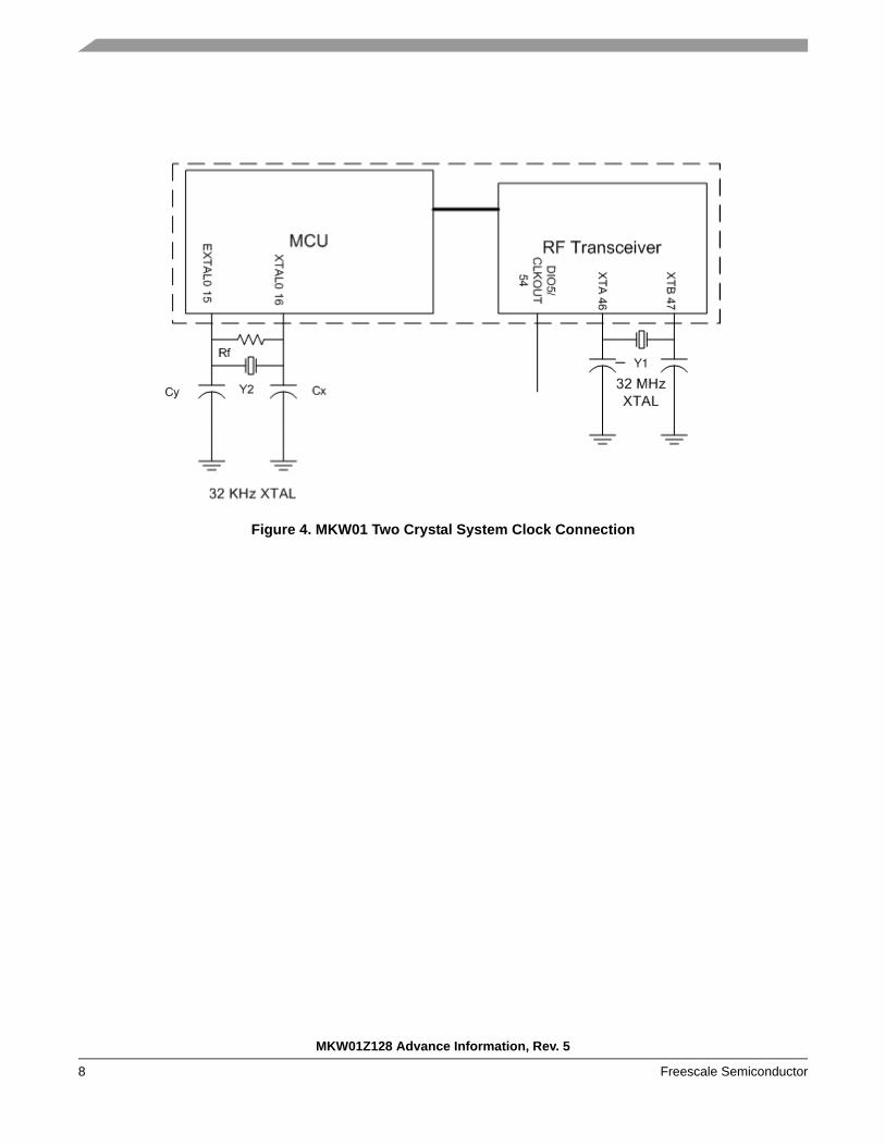
The MKW01 device allows for various system clock configurations:
• Pins 46 & 47 are provided to input a 32 or 30 MHz crystal for the transceiver reference clock source (required) as shown in Figure 3.
• The transceiver can be programmed to provide a programmable frequency clock output (DIO5 which alternates as CLKOUT, pin 54) that can be used as an external source to the CPU (see Figure 3 and Figure 4). As a result, a single crystal system clock solution is possible where the transceiver reference clock source. Routing CLKOUT to the MCU without dividing it is recommended, but it can be divided by 2, 4, 8, 16 and 32.
• The MCU provides a trimmable internal reference clock and also supports an external clock source. An optional on-chip frequency locked loop (FLL) can be used with either clock source to support a CPU clock as high as 48 MHz at 3.6 V.
• Pins 16 and 15 are available to provide an external 32.768 kHz external clock source for the MCU.
Figure 3. MKW01 Single Crystal System Clock Connection
MKW01Z128 Advance Information, Rev. 5
8 Freescale Semiconductor
Figure 4. MKW01 Two Crystal System Clock Connection

MKW01Z128 Advance Information, Rev. 5
Freescale Semiconductor 9
5 MKW01 Pin Assignments and ConnectionsFigure 5 shows the MKW01 pinout.
Figure 5. MKW01 Pinout (Top View)

MKW01Z128 Advance Information, Rev. 5
10 Freescale Semiconductor
5.1 Pin Definitions
Table 1 details the MKW01 pinout and functionality.
Table 1. Pin Function Description (Sheet 1 of 5)
Pin Pin Name1 Type Description Functionality
1 VREFH Input MCU high reference voltage for ADC
2 VREFL Input MCU low reference voltage for ADC
3 VSSA Power Input MCU ADC Ground Connect to ground
4 VSS Power Input MCU Ground Connect to ground
5 PTE16/ADC0_DP1/ADCO_SE1/SPI0_PCS0/TPM/UART2_TX
Digital Input / Output
MCU Port E Bit 16 / ADC0 Single Ended analog channel input DP1/ ADC0 Single Ended analog channel input SE1 / SPI module 0 PCS0 / TPM module Clock In 0 / UART2_TX
6 PTE17/ADC0_DM1/ADCO_SE5a/SPI0_SCK/ TPM_CLKIN1/UART2_RX/LPTMR0_ALT3
Digital Input / Output
MCU Port E Bit 17 / ADC0 Single Ended analog channel input DM1/ ADC0 Single Ended analog channel input 5a / SPI module 0 SCK / TPM module Clock In 1 / UART2_RX / Low Power Timer Module 0 ALT3
7 PTE18/ADC0_DP2/ADC0_SE2/SPI0_MOSI/IIC0_SDA/SPI0_MISO
Digital Input / Output
MCU Port E Bit 18 / ADC0 Single Ended analog channel input DP2/ ADC0 Single Ended analog channel input 2 / SPI module 0 MOSI / IIC0 Bus Data / SPI module 0 MISO
8 PTE19/ADC0_DM2/ ADC0_SE6a/SPI0_MISO /IIC0_SCL/ SPI0_MOSI
Digital Input / Output
MCU Port E Bit 19 / ADC0 Single Ended analog channel input DM2/ ADC0 Single Ended analog channel input 6a / SPI module 0 MISO / IIC0 Bus Clock / SPI module 0 MOSI
9 PTE30/DAC0_OUT/ADCO_SE23/ CMP0_IN4/TPM0_CH3/TPM_CLKIN1
Digit-l Input / Output
MCU Port E Bit 30 / DAC0 Output/ ADC0 Single Ended analog channel input 23 / Comparator 0 Analog Voltage Input 4/ TPM Timer module 0 Channel 3 / TPM module Clock In 1
10 PTA0/SWD_CLK/TSI0_CH1/TPM0_CH5
Digital Input / Output
MCU Port A Bit 0 / Serial Wire Data Clock / Touch Screen Interface Channel 1/ TPM module 0 Channel 5
11 PTA3/SWD_DIO/TSI0_CH4/ IIC1_SCL/TPM0_CH0
Digital Input / Output
MCU Port A Bit 3 / Serial Wire Data DIO / Touch Screen Interface Channel 4 / IIC1 Bus Clock / TPM module 0 Channel 0
12 PTA4/NMI_b/TSI0_CH5/ IIC1_SDA/TPM0_CH1
Digital Input / Output
MCU Port A Bit 4/ / Non Maskable Interrupt_ b/Touch Screen Interface Channel 5 /IIC1 Bus Data / TPM module 0 Channel 1

MKW01Z128 Advance Information, Rev. 5
Freescale Semiconductor 11
13 PTA2/TSI0_CH3/UART0_TX/TPM2_CH1
Digital Input / Output
MCU Port A Bit 2/Touch Screen Interface Channel 3/UART module 0 Transmit / TPM module 2 Channel 1
14 PTA1/TSI0_CH2/UART0_RX/TPM2_CH0
Digital Input / Output
MCU Port A Bit 1/Touch Screen Interface Channel 2/UART module 0 Receive / TPM module Channel 0
15 PTA18/EXTAL0/UART1_RX/ TPM_CLKIN0
Digital Input / Output
MCU Port A Bit 18 / EXTAL0/ UART module 1 Receive / TPM module Clock In 0
16 PTA19/XTAL0/UART1_TX/TPM_CLKIN1/LPTMR0_ALT1
Digital Input / Output
MCU Port A Bit 19 / XTAL0/ UART module 1 Transmit / TPM module Clock In 1/Low Power Timer module 0 ALT1
17 PTB0/ADC0_SE8/TSI0_CH0/LLWU_P5/IIC0_SCL/ TPM1_CH0
Digital Input / Output
MCU Port B Bit 0 / ADC0 Single Ended analog channel input SE8 / Touch Screen Interface Channel 0/ Low Leakage Wake Up Port 5 / IIC0 Bus Clock / TPM module 1 Channel 0
18 PTB1/ADCO_SE9/TSI0_CH6/IIC0_SDA/ TPM1_CH1
Digital Input / Output
MCU Port B Bit 1 / ADC0 Single Ended analog channel input SE9 / Touch Screen Interface Channel 6 / IIC0 Bus Data / TPM module 1 Channel 1
19 VDD Power Input MCU VDD supply input Connect to system VDD supply
20 VSS Power Input MCU Ground Connect to ground
21 PTB2/ADC0_SE12/TSI0_CH7/IIC0_SCL/TPM2_CH0
Digital Input/Output
MCU Port B Bit 2 / ADC0 Single Ended analog channel input SE12 / Touch Screen Interface Channel 7 / IIC0 Bus Clock / TPM Timer module 2 Channel 0
22 PTB17/TSI0_CH10/SPI1_MISO/UART0_TX/TPM_CLKIN1/SPI1_MOSI
Digital Input/Output
MCU Port B Bit 17 / Touch Screen Interface Channel 10/SPI1 MOSI or MISO/UART0 TX / TPM timer clock
23 PTC4/LLWU_P8/SPI0_PCS0/UART1_TX/TPM0_CH3
Digital Input / Output
MCU Port C bit 4 / Low leakage Wake Up port 8 / SPI0 Chip Select / UART1 TX / TPM Timer module 0 channel 3
24 PTC1/ADC0_SE15/TSI0_CH14/LLWU_P6/RTC_CLKIN/ IIC1_SCL/TPM0_CH0
Digital Input Output / Analog Input
MCU Port C Bit 1 /ADC0 Single Ended analog channel input SE15/ Touch Screen Interface Channel 14/ Low Leakage Wake Up Port 6 / Real Time Counter Clock Input/ IC1 Bus Clock/ TPM module 0 Channel 0
25 PTC2/ADC0_SE11/TSI0_CH15/IIC1_SDA/TPM0_CH1
Digital Input / Output / Analog Input
MCU Port C Bit 2 / ADC0 Single Ended analog channel input SE11/ / Touch Screen Interface Channel 15 / IIC1 Bus Data / TPM module 0 Channel 1
Table 1. Pin Function Description (Sheet 2 of 5)
Pin Pin Name1 Type Description Functionality

MKW01Z128 Advance Information, Rev. 5
12 Freescale Semiconductor
26 PTC3/LLWU_P7/UART1_RX/TPM0_CH2/CLKOUTa
Digital Input / Output
MCU Port C Bit 3 / Low Leakage Wake Up Port 7 / UART module 1 Receive / TPM module 0 Channel 2/ Clock OutA
27 PTD4/LLWU_P14/SPI1_PCS0/UART2_RX/TPM0_CH4
Digital Input / Output
MCU Port D Bit 4 / Low Leak Wake Up Port 14/ SPI module 1 PCS0 / UART2 Receiver input / TPM module 0 Channel 4
28 PTD5/ADC0_SE6b/SPI1_SCK/UART2_TX/TPM0_CH5
Digital Input / Output / Analog Input
MCU Port D bit 5 / ADC0 Single Ended analog channel input SE6b / SPI1 clock / UART2 TX / TPM module 0 Channel 5
29 PTD6/ADC0_SE7b/LLWU_P15/SPI1_MOSI/UART0_RX/SPI1_MISO
Digital Input / Output / Analog Input
MCU Port D bit 6 / ADC0 Single Ended analog channel input SE7b / Low leakage Wake Up port 15 / SPI1 MOSI / UART0 RX / SPI module 1 MISO
30 NC No Connect
31 PTD7/SPI0_MISO/UART0_TX/SPI1_MOSI
Digital Input/Output
MCU Port D Bit 7 / SPI module 0 MISO / UART module 0 Transmit / SPI module 1 MOSI
32 PTE0/SPI1_MISO/UART1_TX/RTC_CLKOUT/CMP0_OUT/ IIC1_SDA
Digital Input/Output
MCU Port E Bit 0 / SPI module 1 MISO / UART module 1 Transmit / Real Time Counter Clock Output / Comparator 0 Analog voltage Output / IIC1 Bus Data
33 PTA20/RESETB Digital Input/Output
MCU Port A Bit 20/MCU RESET
34 PTE1 / SPI1_MOSI / UART1_RX /SPI1_MISO / IIC1_SCL
Digital Input/Output
MCU Port E Bit 1 / SPI module 1 MOSI / UART module 1 RX / SPI1_MISO / IIC1_SCL
35 VBAT2 (RF) Power Input Transceiver VDD Connect to system VDD supply
36 GND/SCAN (RF) Power Input Transceiver Ground Connect to ground
37 RXTX (RF) Digital Output
Transceiver Rx / Tx RF Switch Control Output; high when in TX
38 GND_PA2 (RF) Power Input Transceiver RF Ground Connect to ground
39 RFIO (RF) RF Input / Output
Transceiver RF Input / Output
40 GND_PA1 (RF) Power Input Transceiver RF Ground Connect to ground
41 PA_BOOST (RF) RF Output Transceiver Optional High-Power PA Output
42 VR_PA (RF) Power Output
Transceiver regulated output voltage for VR_PA use.
De-coupling cap suggested.
43 VBAT1 (RF) Power Input Transceiver VDD for RF circuitry Connect to system VDD supply
Table 1. Pin Function Description (Sheet 3 of 5)
Pin Pin Name1 Type Description Functionality

MKW01Z128 Advance Information, Rev. 5
Freescale Semiconductor 13
44 VR_ANA (RF) Power Output
Transceiver regulated output voltage for analog circuitry.
Decouple to ground with 100 nF capacitor
45 VR_DIG (RF) Power Output
Transceiver regulated output voltage for digital circuitry.
Decouple to ground with 100 nF capacitor
46 XTA (RF) Xtal Osc Transceiver crystal reference oscillator Connect to 32 MHz crystal and load capacitor
47 XTB (RF) Xtal Osc Transceiver crystal reference oscillator Connect to 32 MHz crystal and load capacitor
48 RESET (RF) Digital Input Transceiver hardware reset input Typically driven from MCU GPIO
49 DIO0/PTE2/SPI1_SCK Digital Input/Output
Internally connected to Transceiver GPIO bit 0 and MCU Port E bit 2 / SPI1 clock
MCU IO and Transceiver IO connected in-package
50 DIO1/PTE3/SPI1_MISO/SPI1_MOSI
Digital Input/Output
Internally connected to Transceiver GPIO bit 1 and MCU Port E bit 3 /SPI1 in or out
MCU IO and Transceiver IO connected in-package
51 DIO2 Digital Input/Output
Transceiver GPIO Bit 2
52 DIO3 Digital Input/Output
Transceiver GPIO Bit 3
53 DIO4 Digital Input/Output
Transceiver GPIO Bit 4
54 DIO5/CLKOUT Digital Input/Output
Transceiver GPIO Bit 5 / ClkOut Commonly programmed as ClkOut to supply MCU clock; connect to Pin 15
55 VDD Power Input MCU VDD supply Connect to VDD supply
56 VDDAD Power Input MCU Analog supply Connect to Analog supply
57 MISO/PTC7/SPI0_MISO/SPI0_MOSI
Digital Input/Output
Internal SPI data connection from Transceiver MISO bit 1 to MCU SPI0 (Port C bit 7 )
• MCU IO and Transceiver IO connected in-package
• MCU IO must be configured for this connection
58 NSS/PTD0/SPI0_PCS0 Digital Input/Output
Internal SPI select connection between Transceiver NSS and MCU SPI0 (Port D bit 0)
• MCU IO and Transceiver IO connected in-package
• MCU IO must be configured for this connection
59 SCK/PTC5/SPI0_SCK Digital Input/Output
Internal SPI clock connection between Transceiver SCK and MCU SPI0 (port C bit 5)
• MCU IO and Transceiver IO connected in-package
• MCU IO must be configured for this connection
Table 1. Pin Function Description (Sheet 4 of 5)
Pin Pin Name1 Type Description Functionality

MKW01Z128 Advance Information, Rev. 5
14 Freescale Semiconductor
5.2 Internal Functional Interconnects
The MCU provides control to the transceiver through the SPI Port and receives status from the transceiver from the DIOx pins. Certain interconnects between the devices are routed on chip. In addition, the signals are brought out to external pads.
NOTE
• As shown in Table 2, the MCU SPI Port pin selection must be configured by software.
• The transceiver DIO pins must be programmed to provide desired status.
• Enhanced performance can be achieved by additionally routing some DIO pins externally to other GPIO pins.
5.3 External Functional Interconnects
In addition to the in-package device interconnection, other external connections between the MCU and the transceiver are common:
60 MOSI/PTC6/SPI0_MOSI/ SPI0_MISO
Digital Input/Output
Internal SPI data connection to Transceiver MOSI bit 1 to MCU SPI0 (Port C bit 6 )
• MCU IO and Transceiver IO connected in-package
• MCU IO must be configured for this connection
FLAG VSS Power input External package flag. Common VSS Connect to ground.
1 Refer to ADD Table 1-3 for additional pin-out information on default and alternate setting selections.
Table 2. MKW01 Internal Functional Interconnects
Pin MCU SignalTransceiver
SignalDescription
49 DIO0/PTE2/SPI1_SCK
DIO0 Transceiver DIO0 can be programmed to provide status to the MCU
50 DIO1/PTE3/SPI1_MISO/SPI1_MOSI
DIO1 Transceiver DIO1 can be programmed to provide status to the MCU
57 MISO/PTC7/SPI0_MISO/SPI0_MOSI
MISO SPI data from transceiver to MCU
58 NSS/PTD0/SPI0_PCS0
NSS SPI chip select
59 SCK/PTC5/SPI0_SCK
SCK SPI Clock
60 MOSI/PTC6/SPI0_MOSI/SPI0_MISO
MOSI SPI data from MCU to transceiver
Table 1. Pin Function Description (Sheet 5 of 5)
Pin Pin Name1 Type Description Functionality

MKW01Z128 Advance Information, Rev. 5
Freescale Semiconductor 15
1. Freescale recommends driving/controlling the transceiver reset from an MCU GPIO - This allows overriding control of the transceiver from the system application.
2. The other DIO2-DIO4 status and RXTX signals can prove useful for monitoring the transceiver operation - the DIO2-DIO4 signals must be programmed to provide operational status. All signals must be connected externally to appropriate MCU GPIO for this function.
6 System and Power ManagementThe MKW01 consists of an independent transceiver and MCU. The MCU controls the transceiver through programming of the SPI Port, and sets its operational mode through this control channel. Total current draw for the MKW01 is dependent on the operation mode of both devices where different modes allow for different levels of power-down. Some additional features supported are:
• Transceiver Sleep with MCU set at the lowest power state.
• The transceiver mode selection being independent of the MCU’s mode selection.
• The transceiver uses/powers-up the transmitter or receiver only as required.
• MCU peripheral control clock gating being disabled on a module-by-module basis to provide lowest power.
• RTC can be used as wake-up timer.
• LLWU (Low Leakage Wake-up Unit) available.
6.1 MCU Power Modes
The MCU has 9 different modes of operation to allow the user to optimize power consumption for the level of functionality needed. Depending on the STOP requirements of the user application, a variety of STOP modes are available that provide state retention, partial power down or full power down of certain logic and/or memory. I/O states are held in all modes of operation. Table 3 outlines the various available power modes of MCU operation.
For each RUN mode there is a corresponding WAIT and STOP mode. WAIT modes are similiar to ARM sleep modes. STOP modes (VLPS, STOP) are similiar to ARM sleep deep mode. The very low power run (VLPR) operating mode can greatly reduce runtime power when the maximum bus frequency is not required to handle application needs. The 3 primary modes of operation are RUN, WAIT and STOP. The WFI instruction invokes both WAIT and STOP modes for the MCU. The primary modes are augmented in a number of ways to provide lower power based on application needs.

MKW01Z128 Advance Information, Rev. 5
16 Freescale Semiconductor
Table 3. MCU power modes
Chip Power Mode
Description Core ModeNormal
Recovery Method
Normal run Allows maximum performance of chip. Default mode out of reset; onchip voltage regulator is on.
Run —
Normal Wait - via WFI
Allows peripherals to function while the core is in sleep mode, reducing power. NVIC remains sensitive to interrupts; peripherals continue to be clocked.
Sleep Interrupt
Normal Stop - via WFI
Places chip in static state. Lowest power mode that retains all registers while maintaining LVD protection. NVIC is disabled; AWIC is used to wake up from interrupt; peripheral clocks are stopped.
Sleep Deep Interrupt
VLPR (Very Low Power Run)
On-chip voltage regulator is in a low power mode that supplies only enough power to run the chip at a reduced frequency. Reduced frequency Flash access mode (1 MHz); LVD off; in BLPI clock mode, the fast internal reference oscillator is available to provide a low power nominal 4 MHz source for the core with the nominal bus and flash clock required to be <800 kHz; alternatively, BLPE clock mode can be used with an external clock or the crystal oscillator providing the clock source.
Run —
VLPW (Very Low Power Wait) -via
WFI
Same as VLPR but with the core in sleep mode to further reducepower; NVIC remains sensitive to interrupts (FCLK = ON). On-chip voltage regulator is in a low power mode that supplies only enough power to run the chip at a reduced frequency.
Sleep Interrupt
VLPS (Very Low Power Stop)-via
WFI
Places chip in static state with LVD operation off. Lowest power mode with ADC and pin interrupts functional. Peripheral clocks are stopped, but OSC, LPTMR, RTC, CMP, TSI can be used. TPM and UART can optionally be enabled if their clock source is enabled. NVIC is disabled (FCLK = OFF); AWIC is used to wake up from interrupt. On-chip voltage regulator is in a low power mode that supplies only enough power to run the chip at a reduced frequency. All SRAM is operating (content retained and I/O states held).
Sleep Deep Interrupt
LLS (Low Leakage Stop)
State retention power mode. Most peripherals are in state retention mode (with clocks stopped), but OSC, LLWU, LPTMR, RTC, CMP,, TSI can be used. NVIC is disabled; LLWU is used to wake up.
NOTE: The LLWU interrupt must not be masked by the interrupt controller to avoid a scenario where the system does not fully exit stop mode on an LLS recovery.
All SRAM is operating (content retained and I/O states held).
Sleep Deep Wakeup Interrupt1

MKW01Z128 Advance Information, Rev. 5
Freescale Semiconductor 17
VLLS3 (Very Low Leakage
Stop3)
Most peripherals are disabled (with clocks stopped), but OSC, LLWU, LPTMR, RTC, CMP, TSI can be used. NVIC is disabled; LLWU is used to wake up.
SRAM_U and SRAM_L remain powered on (content retained and I/O states held).
Sleep Deep Wakeup Reset2
VLLS1 (Very Low Leakage
Stop1)
Most peripherals are disabled (with clocks stopped), but OSC, LLWU, LPTMR, RTC, CMP, TSI can be used. NVIC is disabled; LLWU is used to wake up. All of SRAM_U and SRAM_L are powered off.
Sleep Deep Wakeup Reset2
VLLS0 (Very Low Leakage
Stop 0)
Most peripherals are disabled (with clocks stopped), but LLWU, LPTMR, RTC, TSI can be used. NVIC is disabled; LLWU is used to wake up.All of SRAM_U and SRAM_L are powered off.LPO disabled, optional POR brown-out detection
Sleep Deep Wakeup Reset2
1 Resumes normal run mode operation by executing the LLWU interrupt service routine.2 Follows the reset flow with the LLWU interrupt flag set for the NVIC.
Table 3. MCU power modes
Chip Power Mode
Description Core ModeNormal
Recovery Method

MKW01Z128 Advance Information, Rev. 5
18 Freescale Semiconductor
6.1.1 Power mode transitions
Figure 6 shows power mode transitions. Any reset always brings the MCU back to normal state run. In RUN, WAIT and STOP modes active power regulation is enabled. The VLPx modes are limited in frequency but offer a lower power operating power mode than normal modes. The LLS and VLLSx modes are the lowest power stop modes based on the amount of logic or memory that is required to be reatined by the application.
Figure 6. Power mode state transition diagram
6.2 Transceiver modes of operation.
The transceiver can be set in numerous modes of operation as described in Table 4. By default, when switching from one mode to another various features are selectively turned on coordinated by a pre-defined optimized sequence using the automatic sequencer. Alternatively, these operating modes can be selected directly by disabling the automatic sequencer.

MKW01Z128 Advance Information, Rev. 5
Freescale Semiconductor 19
An overview of the transceiver modes of operation is described below:
• Sleep - provides lowest power consumption and is the full power down state.
• Idle - provides very low standby power consumption and has the main voltage regulator and the RC oscillator enabled.
• Standby - similar to Idle with low standby power consumption but has the main voltage regulator and the crystal oscillator enabled.
• FS (Frequency synthesizer) - the frequency synthesizer is alive to shorten startup time to transmit or receive states.
• Transmit - transmitter is active.
• Receive - receiver is active.
6.3 System Protection
The MKW01 provides numerous vehicles to maintain security or a high level of system robustness:
• Standard COP Watchdog reset with option to run from dedicated 1 kHz internal clock source or bus clock. The COP watchdog is intended to force a system reset when the application software fails to execute as expected.
• LVD protection with reset or interrupt; selectable trip points.
• HardFault exception on attempts to execute undefined instructions or access to undefined memory space.
• LOCKUP reset resource from core.
• Flash protection
Table 4. Basic Transceiver modes
Selected Mode Enabled blocks
Sleep None
Stand-by Main regulator and crystal oscillator
Idle Main regulator and RC oscillator
FS Frequency synthesizer
Transmit Frequency synthesizer and transmitter
Receive Frequency synthesizer and receiver
Listen Periodical receive wake-up from Idle operation

MKW01Z128 Advance Information, Rev. 5
20 Freescale Semiconductor
7 Development EnvironmentDevelopment support for the ARM® Cortex M0+ MCU on the MKW01 is configured to provide maximum flexibility as allowed by the restrictions of the pinout and other available resources. One debug interface is supported:
• Two-wire Serial Wire Debug (SWD) interface
Table 5 presents a brief description of the serial wire debug description.
NOTE
Electrical specifications for the SWD lines can be found in the appendix.
8 System Electrical SpecificationThis section details maximum ratings for the 60 pin LGA package and recommended operating conditions, DC characteristics, and AC characteristics for the modem, and the MCU.
8.1 LGA Package Maximum Ratings
Absolute maximum ratings are stress ratings only, and functional operation at the maximum rating is not guaranteed. Stress beyond the limits specified in Table 6 may affect device reliability or cause permanent damage to the device. For functional operating conditions, refer to the remaining tables in this section.
This device contains circuitry protecting against damage due to high static voltage or electrical fields; however, it is advised that normal precautions be taken to avoid application of any voltages higher than maximum-rated voltages to this high-impedance circuit. Reliability of operation is enhanced if unused inputs are tied to an appropriate logic voltage level (for instance, either VSS or VDD) or the programmable pull-up resistor associated with the pin is enabled.
Table 6 shows the maximum ratings for the 60 Pin LGA package.
Table 5. Debug Components Description
Module Type Description
SWCLK Input Serial Wire Clock. This pin is the clock for debug logic when in the Serial Wire Debug mode. This pin is pulled down internally.
SWDIO Input /Output Serial Wire debug data input / output. The SWDIO pin is used by an external debug tool for communication and devive control. This pin is pulled up internally.

MKW01Z128 Advance Information, Rev. 5
Freescale Semiconductor 21
8.2 ESD Protection and Latch-Up Immunity
Although damage from electrostatic discharge (ESD) is much less common on these devices than on early CMOS circuits, normal handling precautions should be used to avoid exposure to static discharge. Qualification tests are performed to ensure that these devices can withstand exposure to reasonable levels of static without suffering any permanent damage.
All ESD testing is in conformity with the JESD22 Stress Test Qualification for Commercial Grade Integrated Circuits. During the device qualification ESD stresses were performed for the human body model (HBM), the machine model (MM) and the charge device model (CDM).
All latchup testing is in conformity with the JESD78 IC Latch-Up Test.
A device is defined as a failure if after exposure to ESD pulses the device no longer meets the device specification.
Table 6. LGA Package Maximum Ratings
Rating Symbol Value Unit
Maximum Junction Temperature TJ 95 C
Storage Temperature Range Tstg -55 to 115 C
Power Supply Voltage VBATT, VDDINT -0.3 to 3.8 Vdc
Digital Input Voltage Vin -0.3 to (VDDINT + 0.3)
RF Input Power Pmax 6 dBm
Note: Maximum Ratings are those values beyond which damage to the device may occur. Functional operation should be restricted to the limits in the Electrical Characteristics or Recommended Operating Conditions tables.
Note: Meets Human Body Model (HBM) = 2 kV. RF input/output pins have no ESD protection.
Table 7. ESD and Latch-up Test Conditions
Model Description Symbol Value Unit
Human Body
Series resistance R1 1500
Storage capacitance C 100 pF
Number of pulses per pin1
1 This number represents a minimum number for both positive pulse(s) and negative pulse(s)
— 1
Machine
Series resistance R1 0
Storage capacitance C 200 pF
Number of pulses per pin1 — 1
Latch-upMinimum input voltage limit – 1.8 V
Maximum input voltage limit 4.32 V

MKW01Z128 Advance Information, Rev. 5
22 Freescale Semiconductor
8.3 Transceiver Electrical Characteristics
The tables below give the electrical specifications of the transceiver under the following conditions: Supply voltage VBAT1= VBAT2=VDD=3.3 V, temperature = 25 °C, FXOSC = 32 MHz, FRF = 915 MHz, Pout = +13dBm, 2-level FSK modulation without pre-filtering, FDA = 5 kHz, Bit Rate = 4.8 kb/s and terminated in a matched 50 Ohm impedance, unless otherwise specified.
NOTE
Unless otherwise specified, the performances in the other frequency bands are similar or better.
8.3.1 Transceiver Recommended Operating Conditions
Table 8. ESD and Latch-Up Protection Characteristics
No. Rating1
1 Parameter is achieved by design characterization on a small sample size from typical devices under typical conditions unless otherwise noted.
Symbol Min Max Unit
1 Human body model (HBM) VHBM 2000 — V
2 Machine model (MM) VMM 200 — V
3 Charge device model (CDM) VCDM 500 — V
4 Latch-up current at TA = 85C ILAT 100 — mA
Table 9. Recommended Operating Conditions
Characteristic Symbol Min Typ Max Unit
Power Supply Voltage (VBATT) 1.8 3.6 Vdc
Operating Temperature Range TA -40 25 85 C
Logic Input Voltage Low VIL 0 - 20% VBATT
V
Logic Input Voltage High VIH 80% VBATT
- VBATT V
Logic Output Voltage Low (Imax = -1 mA) VOL 0 - 10% VBATT
V
Logic Output Voltage High (Imax = 1 mA) VOH 90% VBATT
- VBATT V
Load capacitance on digital ports CL 25 pF
SPI Clock Rate fSPI - - 8.0 MHz
RF Input Power Pmax - - 0 dBm
Crystal Reference Oscillator Frequency fref 32 MHz Only(Some variants may use 30 MHz instead)

MKW01Z128 Advance Information, Rev. 5
Freescale Semiconductor 23
8.3.2 Transceiver Power Consumption
8.3.3 Transceiver Frequency Synthesis
Table 10. Power Supply Current
Characteristic Conditions Symbol Min Typ Max Unit
Supply current in Sleep mode IDDSL - 0.1 1 µA
Supply current in Idle mode RC oscillator enabled IDDIDLE - 1.2 - µA
Supply current in Standby mode Crystal oscillator enabled IDDST - 1.25 1.5 mA
Supply current in Synthesizer mode IDDFS - 9 - mA
Supply current in Receive mode 4.8 kbps500 kbps
IDDR - 1617
- mAmA
Supply current in Transmit mode with appropriate matching, stable across VDD range
RFOP = +17 dBm, on PA_BOOSTRFOP = +13 dBm, on RFIO pinRFOP = +10 dBm, on RFIO pinRFOP = 0 dBm, on RFIO pinRFOP = -1 dBm, on RFIO pin
IDDT -----
9545332016
-----
mAmAmAmAmA
Table 11. Frequency Synthesizer Specification
Characteristic Conditions Symbol Min Typ Max Unit
Synthesizer Frequency Range Programmable, 32 MHz clock FR 290424862
---
340510
1020
MHzMHzMHz
Crystal oscillator frequency FXOSC - 32 - MHz
Crystal oscillator wake-up time TS_OSC - 250 500 µs
Frequency synthesizer wake-up time to PllLock signal
From Standby mode TS_FS - 80 150 µs
Frequency synthesizer hop time at most 10 kHz away from the target
200 kHz step1 MHz step5 MHz step7 MHz step
12 MHz step20 MHz step25 MHz step
TS_HOP -------
20205050808080
-------
µsµsµsµsµsµsµs
Frequency synthesizer step FSTEP = FXOSC/219 FSTEP - 61.0 - Hz
RC Oscillator frequency After calibration FRC - 62.5 - kHz
Bit rate, FSK Programmable BRF 1.2 - 600 kbps
Bit rate, OOK Programmable BRO 1.2 - 32.768 kbps
Frequency deviation, FSK ProgrammableFDA + BRF/2 =< 500 kHz
FDA 0.6 - 300 kHz

MKW01Z128 Advance Information, Rev. 5
24 Freescale Semiconductor
8.3.4 Receiver
All receiver tests are performed with RxBw = 10 kHz (Single Side Bandwidth) as programmed in RegRxBw, receiving a PN15 sequence with a BER of 0.1% (Bit Synchronizer is enabled), unless otherwise specified. The LNA impedance is set to 200 Ohms, by setting bit LnaZin in RegLna to 1. Blocking tests are performed with an unmodulated interferer. The wanted signal power for the Blocking Immunity, ACR, IIP2, IIP3 and AMR tests is set 3 dB above the nominal sensitivity level.
Table 12. Receiver Specification
Characteristic Conditions Symbol Min Typ Max Unit
FSK sensitivity, highest LNA gain FDA = 5 kHz, BR = 1.2 kb/sFDA = 5 kHz, BR = 4.8 kb/sFDA = 40 kHz, BR = 38.4 kb/s
RFS_F ---
-118-114-105
---
dBmdBmdBm
FDA = 5 kHz, BR = 1.2 kb/s 1 - -120 - dBm
OOK sensitivity, highest LNA gain BR = 4.8 kb/s RFS_O - -112 -109 dBm
Co-Channel Rejection CCR -13 -10 - dB
Adjacent Channel Rejection Offset = +/- 25 kHzOffset = +/- 50 kHz
ACR -37
4242
--
dBdB
Blocking Immunity Offset = +/- 1 MHzOffset = +/- 2 MHz
Offset = +/- 10 MHz
BI ---
-45-40-32
---
dBmdBmdBm
Blocking ImmunityWanted signal at sensitivity +16dB
Offset = +/- 1 MHzOffset = +/- 2 MHz
Offset = +/- 10 MHz
---
-36-33-25
---
dBmdBmdBm
AM Rejection , AM modulated interferer with 100% modulation depth, fm = 1 kHz, square
Offset = +/- 1 MHzOffset = +/- 2 MHz
Offset = +/- 10 MHz
AMR ---
-45-40-32
---
dBmdBmdBm
2nd order Input Intercept PointUnwanted tones are 20 MHz above the LO
Lowest LNA gainHighest LNA gain
IIP2 --
+75+35
--
dBmdBm
3rd order Input Intercept pointUnwanted tones are 1MHz and 1.995 MHz above the LO
Lowest LNA gainHighest LNA gain
IIP3 --23
+20-18
--
dBmdBm
Single Side channel filter BW Programmable BW_SSB 2.6 - 500 kHz
Image rejection in OOK mode Wanted signal level = -106 dBm IMR_OOK
27 30 - dB
Receiver wake-up time, from PLL locked state to RxReady
RxBw = 10 kHz, BR = 4.8 kb/sRxBw = 200 kHz, BR = 100 kb/s
TS_RE --
1.796
--
msµs
Receiver wake-up time, from PLL locked state, AGC enabled
RxBw= 10 kHz, BR = 4.8 kb/sRxBw = 200 kHz, BR = 100 kb/s
TS_RE_AGC
- 3.0163
msµs
Receiver wake-up time, from PLL lock state, AGC and AFC enabled
RxBw= 10 kHz, BR = 4.8 kb/sRxBw = 200 kHz, BR = 100 kb/s
TS_RE_AGC&AFC
4.8265
msµs
FEI sampling time Receiver is ready TS_FEI - 4.Tbit - -
AFC Response Time Receiver is ready TS_AFC - 4.Tbit - -

MKW01Z128 Advance Information, Rev. 5
Freescale Semiconductor 25
8.3.5 Transmitter
9 Typical Applications CircuitFigure 7 shows a MKW01 typical applications circuit with and without use of an external power amplifier (PA) (driven by the RF power boost feature). Note a number of circuit features:
1. The two metal flags on the package bottom are independent (unconnected), and as a result, both must be connected to ground.
2. The topology of the external RF matching components is consistent across various frequency bandwidths. Only the component values differ as determined by the desired frequency range.
3. Freescale recommends using a single crystal design (as shown) to minimize systems costs - the circuit must connect transceiver signal DIO5/CLKOUT to the MCU EXTAL input to supply the MCU with a crystal accurate clock source. Also, the MCU initialization must enable the DIO5 pin as the ClkOut function.
Freescale also recommends that the transceiver RESET is driven by an MCU GPIO to provide total hard-ware control of the transceiver. Figure 7 shows GPIO PTE3 (preferred), but any GPIO can be used.
RSSI Response Time Receiver is ready TS_RSSI - 2.Tbit - -
RSSI Dynamic Range AGC enabled Min Max
DR_RSSI --
-1150
--
dBmdBm
1 Set SensitivityBoost in RegTestLna to 0x2D to reduce the noise floor in the receiver
Table 13. Transmitter Specidication
Characteristic Conditions Symbol Min Typ Max Unit
RF output power in 50 ohmsOn RFIO pin
Programmable with 1dB steps MaxMin
RF_OP --
+13-18
--
dBmdBm
Max RF output power, on PA_BOOST pin
With external match to 50 ohms RF_OPH - +17 - dBm
RF output power stability From VDD=1.8V to 3.6V RF_OP - +/-0.3 - dB
Transmitter Phase Noise 50 kHz Offset from carrier 868 / 915 MHz bands 434 / 315 MHz bands
PHN --
-95-99
--
dBc/Hz
Transmitter adjacent channel power (measured at 25 kHz offset)
BT=0.5 . Measurement conditions as defined by EN 300 220-1 V2.1.1
ACP - - -37 dBm
Transmitter wake up time, to the first rising edge of DCLK
Frequency Synthesizer enabled, PaRamp = 10 µs, BR = 4.8 kb/s.
TS_TR - 120 - µs
Table 12. Receiver Specification
Characteristic Conditions Symbol Min Typ Max Unit

MKW01Z128 Advance Information, Rev. 5
26 Freescale Semiconductor
4. The MKW01 provides in-package connection for the DIO1-DIO0 status to the MCU. External connection of DIO4-DIO2 status to MCU GPIO may be useful or required to implement a wireless node communication algorithm. Enhanced performance can be achieved by routing DIO1 and DIO0 externally to GPIO pins PTC4 and PTC3.
5. The transceiver reference oscillator uses the specified 32 MHz1 crystal (pins XTA and XTB).
6. A debug port connector will beprovided for programming the MKW01 MCU FLASH and debugging code via the SWD interface.
Two common RF wiring options are shown in Figure 7:
1. Bi-directional single port operation - this mode uses the bi-directional RF port pin of the MKW01 designated as RFIO. The device transmits and receives through this single port.
— Typical +13 dBm TX output power
— An inductor acts to provide DC power to the transmitter’s output amplifier while also acting as an AC signal block.
— A circuit topology consisting of inductors and capacitors will provide:
– Impedance matching between the RFIO port and the antenna
– Low pass filtering for the transmit output path — when fully populated can implement an elliptic-function low pass filter.
NOTE
• The topology for the RF matching network can be used over the various bands of interest with changes in component values
• Not all indicated components are used at all frequencies
• Refer to MKW01 Sub 1 GHz Low Power Transceiver plus Microcontroller Reference Manual (MKW01xxRM.pdf) for additional information
2. Dual port operation with external amplification - this mode uses the RFIO port pin of the MKW01 typically as the RX input and the auxiliary port PA_BOOST as the TX output. An external PA can optionally be inserted into the transmit path and an external antenna switch is also required.
— The PA_BOOST has typical +17 dBm output power - this is +4 dBm higher than the RFIO and helps achieve higher power at the PA output
— The PA_BOOST transmit path has a similar filter matching network discussed in the single-port to do low pass filtering and impedance match. The above note about components values also applies.
— With separate transmit and receive paths, an antenna switch is required - the RXTX signal or another programmed GPIO can be used to switch paths depending on radio operation.
— The receive side matching network can be simplified as no low pass filtering or harmonic trapping is required as with the transmit and single port networks
1. Or 30 MHz, in some cases.

MK
W01Z
128 A
dva
nce
Info
rma
tion
, Rev. 2
Fre
escale Sem
iconductor
27
Figure 7. MKW01 Application Circuit Options

MKW01Z128MKW01 MCU Section DataSheetSupports the following: MKW01Z128Features• Operating Characteristics
– Voltage range: 1.8 to 3.6 V– Flash write voltage range: 1.8 to 3.6 V– Temperature range (ambient): -40 to 85°C
• Performance– Up to 48 MHz ARM® Cortex-M0+ core
• Memories and memory interfaces– 128 KB program flash memory– 16 KB RAM
• Clocks– 32 kHz to 40 kHz or 3 MHz to 32 MHz crystal
oscillator– Multi-purpose clock source
• System peripherals– Nine low-power modes to provide power
optimization based on application requirements– 4-channel DMA controller, supporting up to 63
request sources– COP Software watchdog– Low-leakage wakeup unit– SWD interface and Micro Trace buffer– Bit Manipulation Engine (BME)
• Security and integrity modules– 80-bit unique identification (ID) number per chip
• Human-machine interface– Low-power hardware touch sensor interface (TSI)– General-purpose input/output
• Analog modules– 16-bit SAR ADC– 12-bit DAC– Analog comparator (CMP) containing a 6-bit DAC
and programmable reference input
• Timers– Six channel Timer/PWM (TPM)– Two 2-channel Timer/PWM (TPM)– Periodic interrupt timers– 16-bit low-power timer (LPTMR)– Real-time clock
• Communication interfaces– One 16-bit serial peripheral communcation (SPI)
module available externally– Two I2C modules– One low power UART module– Two UART modules
Freescale Semiconductor Document Number: MKW01Z128
Data Sheet: Advance Information Rev. 5, 3/2014
This document contains information on a new product. Specifications andinformation herein are subject to change without notice.
© 2013, 2014 Freescale Semiconductor, Inc.

Table of Contents1 General.....................................................................................3
1.1 Voltage and current operating requirements.....................3
1.2 LVD and POR operating requirements..............................3
1.3 Voltage and current operating behaviors...........................4
1.4 Power mode transition operating behaviors......................5
1.5 Power consumption operating behaviors..........................6
1.5.1 Diagram: Typical IDD_RUN operating behavior. . .10
1.6 Designing with radiated emissions in mind........................12
1.7 Capacitance attributes.......................................................12
1.8 Switching specifications.....................................................13
1.8.1 Device clock specifications...................................13
1.8.2 General switching specifications...........................13
2 Peripheral operating requirements and behaviors....................14
2.1 Core modules....................................................................14
2.1.1 SWD electricals ....................................................14
2.2 System modules................................................................15
2.3 Clock modules...................................................................15
2.3.1 MCG specifications...............................................15
2.3.2 Oscillator electrical specifications.........................17
2.4 Memories and memory interfaces.....................................19
2.4.1 Flash electrical specifications................................19
2.5 Security and integrity modules..........................................21
2.6 Analog...............................................................................21
2.6.1 ADC electrical specifications.................................21
2.6.2 CMP and 6-bit DAC electrical specifications.........26
2.6.3 12-bit DAC electrical characteristics.....................28
2.7 Timers................................................................................31
2.8 Communication interfaces.................................................31
2.8.1 SPI switching specifications..................................31
2.8.2 Inter-Integrated Circuit Interface (I2C) timing........35
2.8.3 UART....................................................................36
2.9 Human-machine interfaces (HMI)......................................37
2.9.1 TSI electrical specifications...................................37
MKW01 MCU Section Data Sheet Data Sheet, Rev. 5, 3/2014.
2 Freescale Semiconductor, Inc.
1 General
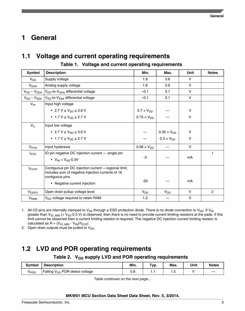
1.1 Voltage and current operating requirementsTable 1. Voltage and current operating requirements
Symbol Description Min. Max. Unit Notes
VDD Supply voltage 1.8 3.6 V
VDDA Analog supply voltage 1.8 3.6 V
VDD – VDDA VDD-to-VDDA differential voltage –0.1 0.1 V
VSS – VSSA VSS-to-VSSA differential voltage –0.1 0.1 V
VIH Input high voltage
• 2.7 V ≤ VDD ≤ 3.6 V
• 1.7 V ≤ VDD ≤ 2.7 V
0.7 × VDD
0.75 × VDD
—
—
V
V
VIL Input low voltage
• 2.7 V ≤ VDD ≤ 3.6 V
• 1.7 V ≤ VDD ≤ 2.7 V
—
—
0.35 × VDD
0.3 × VDD
V
V
VHYS Input hysteresis 0.06 × VDD — V
IICIO IO pin negative DC injection current — single pin
• VIN < VSS-0.3V-3 — mA
1
IICcont Contiguous pin DC injection current —regional limit,includes sum of negative injection currents of 16contiguous pins
• Negative current injection-25 — mA
VODPU Open drain pullup voltage level VDD VDD V 2
VRAM VDD voltage required to retain RAM 1.2 — V
1. All I/O pins are internally clamped to VSS through a ESD protection diode. There is no diode connection to VDD. If VINgreater than VIO_MIN (= VSS-0.3 V) is observed, then there is no need to provide current limiting resistors at the pads. If thislimit cannot be observed then a current limiting resistor is required. The negative DC injection current limiting resistor iscalculated as R = (VIO_MIN - VIN)/|IICIO|.
2. Open drain outputs must be pulled to VDD.
1.2 LVD and POR operating requirementsTable 2. VDD supply LVD and POR operating requirements
Symbol Description Min. Typ. Max. Unit Notes
VPOR Falling VDD POR detect voltage 0.8 1.1 1.5 V —
Table continues on the next page...
General
MKW01 MCU Section Data Sheet Data Sheet, Rev. 5, 3/2014.
Freescale Semiconductor, Inc. 3

Table 2. VDD supply LVD and POR operating requirements (continued)
Symbol Description Min. Typ. Max. Unit Notes
VLVDH Falling low-voltage detect threshold — highrange (LVDV = 01)
2.48 2.56 2.64 V —
VLVW1H
VLVW2H
VLVW3H
VLVW4H
Low-voltage warning thresholds — high range
• Level 1 falling (LVWV = 00)
• Level 2 falling (LVWV = 01)
• Level 3 falling (LVWV = 10)
• Level 4 falling (LVWV = 11)
2.62
2.72
2.82
2.92
2.70
2.80
2.90
3.00
2.78
2.88
2.98
3.08
V
V
V
V
1
VHYSH Low-voltage inhibit reset/recover hysteresis —high range
— ±60 — mV —
VLVDL Falling low-voltage detect threshold — low range(LVDV=00)
1.54 1.60 1.66 V —
VLVW1L
VLVW2L
VLVW3L
VLVW4L
Low-voltage warning thresholds — low range
• Level 1 falling (LVWV = 00)
• Level 2 falling (LVWV = 01)
• Level 3 falling (LVWV = 10)
• Level 4 falling (LVWV = 11)
1.74
1.84
1.94
2.04
1.80
1.90
2.00
2.10
1.86
1.96
2.06
2.16
V
V
V
V
1
VHYSL Low-voltage inhibit reset/recover hysteresis —low range
— ±40 — mV —
VBG Bandgap voltage reference 0.97 1.00 1.03 V —
tLPO Internal low power oscillator period — factorytrimmed
900 1000 1100 μs —
1. Rising thresholds are falling threshold + hysteresis voltage
1.3 Voltage and current operating behaviorsTable 3. Voltage and current operating behaviors
Symbol Description Min. Max. Unit Notes
VOH Output high voltage — Normal drive pad (exceptRESET_b)
• 2.7 V ≤ VDD ≤ 3.6 V, IOH = -5 mA
• 1.8 V ≤ VDD ≤ 2.7 V, IOH = -2.5 mA
VDD – 0.5
VDD – 0.5
—
—
V
V
1, 2
VOH Output high voltage — High drive pad (exceptRESET_b)
• 2.7 V ≤ VDD ≤ 3.6 V, IOH = -20 mA
• 1.8 V ≤ VDD ≤ 2.7 V, IOH = -10 mA
VDD – 0.5
VDD – 0.5
—
—
V
V
1 , 2
IOHT Output high current total for all ports — 100 mA
Table continues on the next page...
General
MKW01 MCU Section Data Sheet Data Sheet, Rev. 5, 3/2014.
4 Freescale Semiconductor, Inc.

Table 3. Voltage and current operating behaviors (continued)
Symbol Description Min. Max. Unit Notes
VOL Output low voltage — Normal drive pad
• 2.7 V ≤ VDD ≤ 3.6 V, IOL = 5 mA
• 1.8 V ≤ VDD ≤ 2.7 V, IOL = 2.5 mA
—
—
0.5
0.5
V
V
1
VOL Output low voltage — High drive pad
• 2.7 V ≤ VDD ≤ 3.6 V, IOL = 20 mA
• 1.8 V ≤ VDD ≤ 2.7 V, IOL = 10 mA
—
—
0.5
0.5
V
V
1
IOLT Output low current total for all ports — 100 mA
IIN Input leakage current (per pin) for full temperaturerange
— 1 μA 3
IIN Input leakage current (per pin) at 25 °C — 0.025 μA 3
IIN Input leakage current (total all pins) for full temperaturerange
— 65 μA 3
IOZ Hi-Z (off-state) leakage current (per pin) — 1 μA
RPU Internal pullup resistors 20 50 kΩ 4
1. The reset pin only contains an active pull down device when configured as the RESET signal or as a GPIO. Whenconfigured as a GPIO output, it acts as a pseudo open drain output.
2. PTB0, PTB1, PTD6, and PTD7 I/O have both high drive and normal drive capability selected by the associatedPTx_PCRn[DSE] control bit. All other GPIOs are normal drive only.
3. Measured at VDD = 3.6 V4. Measured at VDD supply voltage = VDD min and Vinput = VSS
1.4 Power mode transition operating behaviors
All specifications except tPOR and VLLSx→RUN recovery times in the following tableassume this clock configuration:
• CPU and system clocks = 48 MHz• Bus and flash clock = 24 MHz• FEI clock mode
POR and VLLSx→RUN recovery use FEI clock mode at the default CPU and systemfrequency of 21 MHz, and a bus and flash clock frequency of 10.5 MHz.
Table 4. Power mode transition operating behaviors
Symbol Description Min. Typ. Max. Unit Notes
tPOR After a POR event, amount of time from the pointVDD reaches 1.8 V to execution of the firstinstruction across the operating temperaturerange of the chip.
— — 300 μs 1
Table continues on the next page...
General
MKW01 MCU Section Data Sheet Data Sheet, Rev. 5, 3/2014.
Freescale Semiconductor, Inc. 5

Table 4. Power mode transition operating behaviors (continued)
Symbol Description Min. Typ. Max. Unit Notes
• VLLS0 → RUN
—
106
120
μs
• VLLS1 → RUN
—
105
117
μs
• VLLS3 → RUN
—
47
54
μs
• LLS → RUN
—
4.5
5.0
μs
• VLPS → RUN
—
4.5
5.0
μs
• STOP → RUN
—
4.5
5.0
μs
1. Normal boot (FTFA_FOPT[LPBOOT]=11).
1.5 Power consumption operating behaviorsTable 5. Power consumption operating behaviors
Symbol Description Min. Typ. Max. Unit Notes
IDDA Analog supply current — — See note mA 1
IDD_RUNCO_
CM
Run mode current in compute operation - 48MHz core / 24 MHz flash / bus disabled, LPTMRrunning using 4 MHz internal reference clock,CoreMark benchmark code executing from flash
• at 3.0 V
—
6.1
—
mA
2
IDD_RUNCO Run mode current in compute operation - 48MHz core / 24 MHz flash / bus clock disabled,code of while(1) loop executing from flash
• at 3.0 V
—
3.8
5.9
mA
3
IDD_RUN Run mode current - 48 MHz core / 24 MHz busand flash, all peripheral clocks disabled, code ofwhile(1) loop executing from flash
• at 3.0 V
—
4.6
6.1
mA
3
Table continues on the next page...
General
MKW01 MCU Section Data Sheet Data Sheet, Rev. 5, 3/2014.
6 Freescale Semiconductor, Inc.

Table 5. Power consumption operating behaviors (continued)
Symbol Description Min. Typ. Max. Unit Notes
IDD_RUN Run mode current - 48 MHz core / 24 MHz busand flash, all peripheral clocks enabled, code ofwhile(1) loop executing from flash
• at 3.0 V
• at 25 °C
• at 70 °C
• at 125 °C
—
—
—
6.0
6.2
6.3
6.5
6.8
7.1
mA
mA
mA
3, 4
IDD_WAIT Wait mode current - core disabled / 48 MHzsystem / 24 MHz bus / flash disabled (flash dozeenabled), all peripheral clocks disabled
• at 3.0 V
— 2.7 5.7 mA3
IDD_WAIT Wait mode current - core disabled / 24 MHzsystem / 24 MHz bus / flash disabled (flash dozeenabled), all peripheral clocks disabled
• at 3.0 V
— 2.1 5.5 mA3
IDD_PSTOP2 Stop mode current with partial stop 2 clockingoption - core and system disabled / 10.5 MHzbus
• at 3.0 V
— 2.2 4.1 mA3
IDD_VLPRCO
_CM
Very-low-power run mode current in computeoperation - 4 MHz core / 0.8 MHz flash / busclock disabled, LPTMR running with 4 MHzinternal reference clock, CoreMark benchmarkcode executing from flash
• at 3.0 V
— 732 — μA5
IDD_VLPRCO Very-low-power run mode current in computeoperation - 4 MHz core / 0.8 MHz flash / busclock disabled, code of while(1) loop executingfrom flash
• at 3.0 V
— 161 367 μA6
IDD_VLPR Very-low-power run mode current - 4 MHz core /0.8 MHz bus and flash, all peripheral clocksdisabled, code of while(1) loop executing fromflash
• at 3.0 V
— 185 372 μA6
IDD_VLPR Very-low-power run mode current - 4 MHz core /0.8 MHz bus and flash, all peripheral clocksenabled, code of while(1) loop executing fromflash
• at 3.0 V
— 256 420 μA4, 6
IDD_VLPW Very-low-power wait mode current - coredisabled / 4 MHz system / 0.8 MHz bus / flashdisabled (flash doze enabled), all peripheralclocks disabled
• at 3.0 V
— 110 355 μA 6
Table continues on the next page...
General
MKW01 MCU Section Data Sheet Data Sheet, Rev. 5, 3/2014.
Freescale Semiconductor, Inc. 7

Table 5. Power consumption operating behaviors (continued)
Symbol Description Min. Typ. Max. Unit Notes
IDD_STOP Stop mode current at 3.0 V
at 25 °C
at 50 °C
at 70 °C
at 85 °C
—
—
—
—
301
311
342
382
428
722
758
809
μA
IDD_VLPS Very-low-power stop mode current at 3.0 V
at 25 °C
at 50 °C
at 70 °C
at 85 °C
—
—
—
—
2.3
5.2
10.5
19.3
8.4
18.3
26.1
58.5
μA
IDD_LLS Low-leakage stop mode current at 3.0 V
at 25 °C
at 50 °C
at 70 °C
at 85 °C
—
—
—
—
1.7
3.2
5.8
11.6
3.3
34.9
38.5
43.8
μA
IDD_VLLS3 Very-low-leakage stop mode 3 current at 3.0 V
at 25 °C
at 50 °C
at 70 °C
at 85 °C
—
—
—
—
1.3
2.3
4.7
8.5
3.0
17.6
19.5
24.1
μA
IDD_VLLS1 Very-low-leakage stop mode 1 current at 3.0V
at 25°C
at 50°C
at 70°C
at 85°C
—
—
—
—
0.7
1.2
2.2
4.8
1.3
11.7
12.6
15.3
μA
IDD_VLLS0 Very-low-leakage stop mode 0 current(SMC_STOPCTRL[PORPO] = 0) at 3.0 V
at 25 °C
at 50 °C
at 70 °C
at 85 °C
—
—
—
—
310
778
1928
3906
844
3861
13055
15457
nA
IDD_VLLS0 Very-low-leakage stop mode 0 current(SMC_STOPCTRL[PORPO] = 1) at 3.0 V
at 25 °C
at 50 °C
at 70 °C
at 85 °C
—
—
—
—
139
600
1674
3554
747
3418
11143
13683
nA
7
General
MKW01 MCU Section Data Sheet Data Sheet, Rev. 5, 3/2014.
8 Freescale Semiconductor, Inc.

1. The analog supply current is the sum of the active or disabled current for each of the analog modules on the device. Seeeach module's specification for its supply current.
2. MCG configured for PEE mode. CoreMark benchmark compiled using IAR 6.40 with optimization level high, optimized forbalanced.
3. MCG configured for FEI mode.4. Incremental current consumption from peripheral activity is not included.5. MCG configured for BLPI mode. CoreMark benchmark compiled using IAR 6.40 with optimization level high, optimized for
balanced.6. MCG configured for BLPI mode.7. No brownout
Table 6. Low power mode peripheral adders — typical value
Symbol Description Temperature (°C) Unit
-40 25 50 70 85
IIREFSTEN4MHz 4 MHz internal reference clock (IRC) adder.Measured by entering STOP or VLPS modewith 4 MHz IRC enabled.
56 56 56 56 56 µA
IIREFSTEN32KHz 32 kHz internal reference clock (IRC)adder. Measured by entering STOP modewith the 32 kHz IRC enabled.
52 52 52 52 52 µA
IEREFSTEN4MHz External 4 MHz crystal clock adder.Measured by entering STOP or VLPS modewith the crystal enabled.
250 262 266 268 272 uA
IEREFSTEN32KHz External 32 kHz crystal clock adder bymeans of the OSC0_CR[EREFSTEN andEREFSTEN] bits. Measured by entering allmodes with the crystal enabled.
VLLS1
VLLS3
LLS
VLPS
STOP
440
440
490
510
510
490
490
490
560
560
540
540
540
560
560
560
560
560
560
560
570
570
570
610
610
nA
ICMP CMP peripheral adder measured by placingthe device in VLLS1 mode with CMPenabled using the 6-bit DAC and a singleexternal input for compare. Includes 6-bitDAC power consumption.
22 22 22 22 22 µA
IRTC RTC peripheral adder measured by placingthe device in VLLS1 mode with external 32kHz crystal enabled by means of theRTC_CR[OSCE] bit and the RTC ALARMset for 1 minute. Includes ERCLK32K (32kHz external crystal) power consumption.
432 357 388 475 532 nA
IUART UART peripheral adder measured byplacing the device in STOP or VLPS modewith selected clock source waiting for RXdata at 115200 baud rate. Includes selectedclock source power consumption.
MCGIRCLK (4 MHz internal referenceclock)
OSCERCLK (4 MHz external crystal)
66
259
66
271
66
275
66
277
66
281
µA
Table continues on the next page...
General
MKW01 MCU Section Data Sheet Data Sheet, Rev. 5, 3/2014.
Freescale Semiconductor, Inc. 9

Table 6. Low power mode peripheral adders — typical value (continued)
Symbol Description Temperature (°C) Unit
-40 25 50 70 85
ITPM TPM peripheral adder measured by placingthe device in STOP or VLPS mode withselected clock source configured for outputcompare generating 100 Hz clock signal.No load is placed on the I/O generating theclock signal. Includes selected clock sourceand I/O switching currents.
MCGIRCLK (4 MHz internal referenceclock)
OSCERCLK (4 MHz external crystal)
86
275
86
288
86
290
86
295
86
300
µA
IBG Bandgap adder when BGEN bit is set anddevice is placed in VLPx, LLS, or VLLSxmode.
45 45 45 45 45 µA
IADC ADC peripheral adder combining themeasured values at VDD and VDDA byplacing the device in STOP or VLPS mode.ADC is configured for low-power modeusing the internal clock and continuousconversions.
366 366 366 366 366 µA
1.5.1 Diagram: Typical IDD_RUN operating behavior
The following data was measured under these conditions:
• No GPIOs toggled• Code execution from flash with cache enabled• For the ALLOFF curve, all peripheral clocks are disabled except FTFA
General
MKW01 MCU Section Data Sheet Data Sheet, Rev. 5, 3/2014.
10 Freescale Semiconductor, Inc.

Figure 1. Run mode supply current vs. core frequency
General
MKW01 MCU Section Data Sheet Data Sheet, Rev. 5, 3/2014.
Freescale Semiconductor, Inc. 11
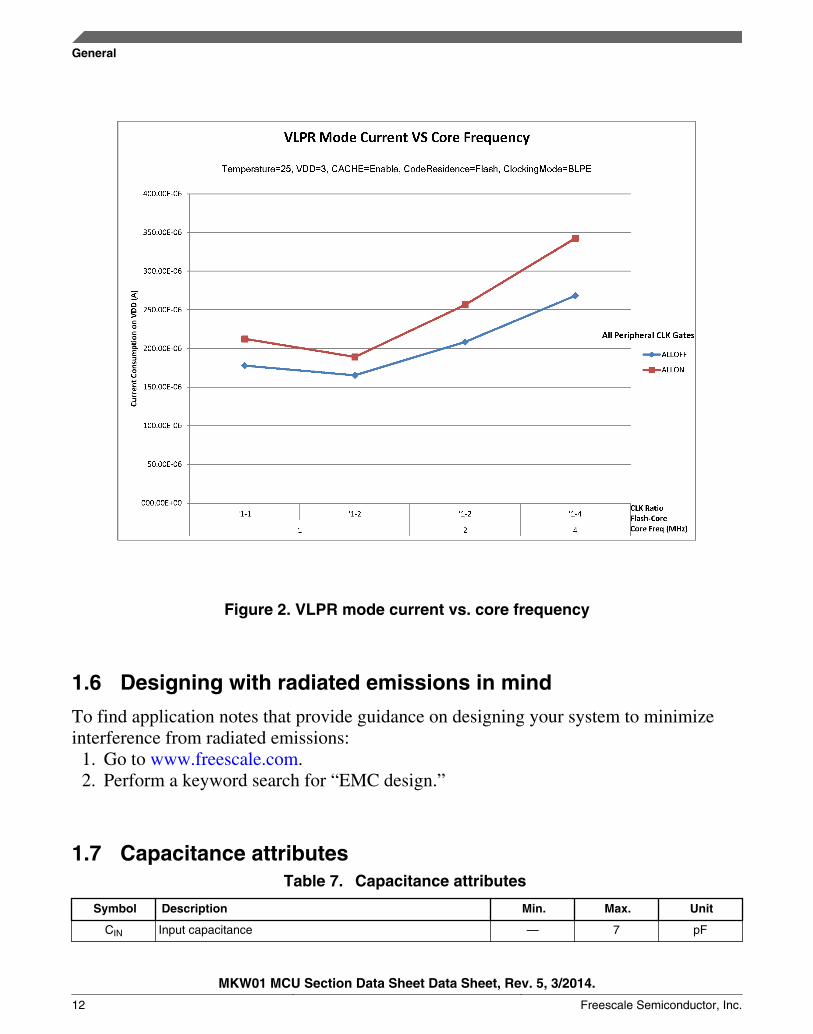
Figure 2. VLPR mode current vs. core frequency
1.6 Designing with radiated emissions in mind
To find application notes that provide guidance on designing your system to minimizeinterference from radiated emissions:
1. Go to www.freescale.com.2. Perform a keyword search for “EMC design.”
1.7 Capacitance attributesTable 7. Capacitance attributes
Symbol Description Min. Max. Unit
CIN Input capacitance — 7 pF
General
MKW01 MCU Section Data Sheet Data Sheet, Rev. 5, 3/2014.
12 Freescale Semiconductor, Inc.
1.8 Switching specifications
1.8.1 Device clock specificationsTable 8. Device clock specifications
Symbol Description Min. Max. Unit
Normal run mode
fSYS System and core clock — 48 MHz
fBUS Bus clock — 24 MHz
fFLASH Flash clock — 24 MHz
fLPTMR LPTMR clock — 24 MHz
VLPR and VLPS modes1
fSYS System and core clock — 4 MHz
fBUS Bus clock — 1 MHz
fFLASH Flash clock — 1 MHz
fLPTMR LPTMR clock2 — 24 MHz
fERCLK External reference clock — 16 MHz
fLPTMR_ERCLK LPTMR external reference clock — 16 MHz
fosc_hi_2 Oscillator crystal or resonator frequency — high frequencymode (high range) (MCG_C2[RANGE]=1x)
— 16 MHz
fTPM TPM asynchronous clock — 8 MHz
fUART0 UART0 asynchronous clock — 8 MHz
1. The frequency limitations in VLPR and VLPS modes here override any frequency specification listed in the timingspecification for any other module. These same frequency limits apply to VLPS, whether VLPS was entered from RUN orfrom VLPR.
2. The LPTMR can be clocked at this speed in VLPR or VLPS only when the source is an external pin.
1.8.2 General switching specifications
These general-purpose specifications apply to all signals configured for GPIO and UARTsignals.
Table 9. General switching specifications
Description Min. Max. Unit Notes
GPIO pin interrupt pulse width (digital glitch filter disabled) —Synchronous path
1.5 — Bus clockcycles
1
External RESET and NMI pin interrupt pulse width —Asynchronous path
100 — ns 2
Table continues on the next page...
General
MKW01 MCU Section Data Sheet Data Sheet, Rev. 5, 3/2014.
Freescale Semiconductor, Inc. 13

Table 9. General switching specifications (continued)
Description Min. Max. Unit Notes
GPIO pin interrupt pulse width — Asynchronous path 16 — ns 2
Port rise and fall time — 36 ns 3
1. The greater synchronous and asynchronous timing must be met.2. This is the shortest pulse that is guaranteed to be recognized.3. 75 pF load
2 Peripheral operating requirements and behaviors
2.1 Core modules
2.1.1 SWD electricalsTable 10. SWD full voltage range electricals
Symbol Description Min. Max. Unit
Operating voltage 1.8 3.6 V
J1 SWD_CLK frequency of operation
• Serial wire debug
0
25
MHz
J2 SWD_CLK cycle period 1/J1 — ns
J3 SWD_CLK clock pulse width
• Serial wire debug
20
—
ns
J4 SWD_CLK rise and fall times — 3 ns
J9 SWD_DIO input data setup time to SWD_CLK rise 10 — ns
J10 SWD_DIO input data hold time after SWD_CLK rise 0 — ns
J11 SWD_CLK high to SWD_DIO data valid — 32 ns
J12 SWD_CLK high to SWD_DIO high-Z 5 — ns
J2
J3 J3
J4 J4
SWD_CLK (input)
Figure 3. Serial wire clock input timing
Peripheral operating requirements and behaviors
MKW01 MCU Section Data Sheet Data Sheet, Rev. 5, 3/2014.
14 Freescale Semiconductor, Inc.
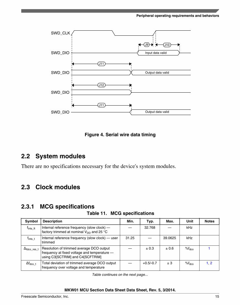
J11
J12
J11
J9 J10
Input data valid
Output data valid
Output data valid
SWD_CLK
SWD_DIO
SWD_DIO
SWD_DIO
SWD_DIO
Figure 4. Serial wire data timing
2.2 System modules
There are no specifications necessary for the device's system modules.
2.3 Clock modules
2.3.1 MCG specificationsTable 11. MCG specifications
Symbol Description Min. Typ. Max. Unit Notes
fints_ft Internal reference frequency (slow clock) —factory trimmed at nominal VDD and 25 °C
— 32.768 — kHz
fints_t Internal reference frequency (slow clock) — usertrimmed
31.25 — 39.0625 kHz
Δfdco_res_t Resolution of trimmed average DCO outputfrequency at fixed voltage and temperature —using C3[SCTRIM] and C4[SCFTRIM]
— ± 0.3 ± 0.6 %fdco 1
Δfdco_t Total deviation of trimmed average DCO outputfrequency over voltage and temperature
— +0.5/-0.7 ± 3 %fdco 1, 2
Table continues on the next page...
Peripheral operating requirements and behaviors
MKW01 MCU Section Data Sheet Data Sheet, Rev. 5, 3/2014.
Freescale Semiconductor, Inc. 15

Table 11. MCG specifications (continued)
Symbol Description Min. Typ. Max. Unit Notes
Δfdco_t Total deviation of trimmed average DCO outputfrequency over fixed voltage and temperaturerange of 0–70 °C
— ± 0.4 ± 1.5 %fdco 1, 2
fintf_ft Internal reference frequency (fast clock) —factory trimmed at nominal VDD and 25 °C
— 4 — MHz
Δfintf_ft Frequency deviation of internal reference clock(fast clock) over temperature and voltage —factory trimmed at nominal VDD and 25 °C
— +1/-2 ± 3 %fintf_ft
2
fintf_t Internal reference frequency (fast clock) — usertrimmed at nominal VDD and 25 °C
3 — 5 MHz
floc_low Loss of external clock minimum frequency —RANGE = 00
(3/5) xfints_t
— — kHz
floc_high Loss of external clock minimum frequency —RANGE = 01, 10, or 11
(16/5) xfints_t
— — kHz
FLL
ffll_ref FLL reference frequency range 31.25 — 39.0625 kHz
fdco DCO outputfrequency range
Low range (DRS = 00)
640 × ffll_ref
20 20.97 25 MHz 3, 4
Mid range (DRS = 01)
1280 × ffll_ref
40 41.94 48 MHz
fdco_t_DMX32 DCO outputfrequency
Low range (DRS = 00)
732 × ffll_ref
— 23.99 — MHz 5, 6
Mid range (DRS = 01)
1464 × ffll_ref
— 47.97 — MHz
Jcyc_fll FLL period jitter
• fVCO = 48 MHz
— 180 — ps 7
tfll_acquire FLL target frequency acquisition time — — 1 ms 8
PLL
fvco VCO operating frequency 48.0 — 100 MHz
Ipll PLL operating current• PLL at 96 MHz (fosc_hi_1 = 8 MHz, fpll_ref = 2
MHz, VDIV multiplier = 48)
— 1060 — µA9
Ipll PLL operating current• PLL at 48 MHz (fosc_hi_1 = 8 MHz, fpll_ref = 2
MHz, VDIV multiplier = 24)
— 600 — µA9
fpll_ref PLL reference frequency range 2.0 — 4.0 MHz
Jcyc_pll PLL period jitter (RMS)
• fvco = 48 MHz
• fvco = 100 MHz
—
—
120
50
—
—
ps
ps
10
Jacc_pll PLL accumulated jitter over 1µs (RMS)
• fvco = 48 MHz
• fvco = 100 MHz
—
—
1350
600
—
—
ps
ps
10
Table continues on the next page...
Peripheral operating requirements and behaviors
MKW01 MCU Section Data Sheet Data Sheet, Rev. 5, 3/2014.
16 Freescale Semiconductor, Inc.
Table 11. MCG specifications (continued)
Symbol Description Min. Typ. Max. Unit Notes
Dlock Lock entry frequency tolerance ± 1.49 — ± 2.98 %
Dunl Lock exit frequency tolerance ± 4.47 — ± 5.97 %
tpll_lock Lock detector detection time — — 150 × 10-6
+ 1075(1/fpll_ref)
s 11
1. This parameter is measured with the internal reference (slow clock) being used as a reference to the FLL (FEI clockmode).
2. The deviation is relative to the factory trimmed frequency at nominal VDD and 25 °C, fints_ft.3. These typical values listed are with the slow internal reference clock (FEI) using factory trim and DMX32 = 0.4. The resulting system clock frequencies must not exceed their maximum specified values. The DCO frequency deviation
(Δfdco_t) over voltage and temperature must be considered.5. These typical values listed are with the slow internal reference clock (FEI) using factory trim and DMX32 = 1.6. The resulting clock frequency must not exceed the maximum specified clock frequency of the device.7. This specification is based on standard deviation (RMS) of period or frequency.8. This specification applies to any time the FLL reference source or reference divider is changed, trim value is changed,
DMX32 bit is changed, DRS bits are changed, or changing from FLL disabled (BLPE, BLPI) to FLL enabled (FEI, FEE,FBE, FBI). If a crystal/resonator is being used as the reference, this specification assumes it is already running.
9. Excludes any oscillator currents that are also consuming power while PLL is in operation.10. This specification was obtained using a Freescale developed PCB. PLL jitter is dependent on the noise characteristics of
each PCB and results will vary.11. This specification applies to any time the PLL VCO divider or reference divider is changed, or changing from PLL disabled
(BLPE, BLPI) to PLL enabled (PBE, PEE). If a crystal/resonator is being used as the reference, this specification assumesit is already running.
2.3.2 Oscillator electrical specifications
2.3.2.1 Oscillator DC electrical specificationsTable 12. Oscillator DC electrical specifications
Symbol Description Min. Typ. Max. Unit Notes
VDD Supply voltage 1.8 — 3.6 V
IDDOSC Supply current — low-power mode (HGO=0)
• 32 kHz
• 4 MHz
• 8 MHz (RANGE=01)
• 16 MHz
• 24 MHz
• 32 MHz
—
—
—
—
—
—
500
200
300
950
1.2
1.5
—
—
—
—
—
—
nA
μA
μA
μA
mA
mA
1
Table continues on the next page...
Peripheral operating requirements and behaviors
MKW01 MCU Section Data Sheet Data Sheet, Rev. 5, 3/2014.
Freescale Semiconductor, Inc. 17

Table 12. Oscillator DC electrical specifications (continued)
Symbol Description Min. Typ. Max. Unit Notes
IDDOSC Supply current — high gain mode (HGO=1)
• 32 kHz
• 4 MHz
• 8 MHz (RANGE=01)
• 16 MHz
• 24 MHz
• 32 MHz
—
—
—
—
—
—
25
400
500
2.5
3
4
—
—
—
—
—
—
μA
μA
μA
mA
mA
mA
1
Cx EXTAL load capacitance — — — 2, 3
Cy XTAL load capacitance — — — 2, 3
RF Feedback resistor — low-frequency, low-powermode (HGO=0)
— — — MΩ 2, 4
Feedback resistor — low-frequency, high-gainmode (HGO=1)
— 10 — MΩ
Feedback resistor — high-frequency, low-powermode (HGO=0)
— — — MΩ
Feedback resistor — high-frequency, high-gainmode (HGO=1)
— 1 — MΩ
RS Series resistor — low-frequency, low-powermode (HGO=0)
— — — kΩ
Series resistor — low-frequency, high-gain mode(HGO=1)
— 200 — kΩ
Series resistor — high-frequency, low-powermode (HGO=0)
— — — kΩ
Series resistor — high-frequency, high-gainmode (HGO=1)
—
0
—
kΩ
Vpp5 Peak-to-peak amplitude of oscillation (oscillator
mode) — low-frequency, low-power mode(HGO=0)
— 0.6 — V
Peak-to-peak amplitude of oscillation (oscillatormode) — low-frequency, high-gain mode(HGO=1)
— VDD — V
Peak-to-peak amplitude of oscillation (oscillatormode) — high-frequency, low-power mode(HGO=0)
— 0.6 — V
Peak-to-peak amplitude of oscillation (oscillatormode) — high-frequency, high-gain mode(HGO=1)
— VDD — V
1. VDD=3.3 V, Temperature =25 °C2. See crystal or resonator manufacturer's recommendation3. Cx,Cy can be provided by using the integrated capacitors when the low frequency oscillator (RANGE = 00) is used. For all
other cases external capacitors must be used.4. When low power mode is selected, RF is integrated and must not be attached externally.5. The EXTAL and XTAL pins should only be connected to required oscillator components and must not be connected to any
other devices.
Peripheral operating requirements and behaviors
MKW01 MCU Section Data Sheet Data Sheet, Rev. 5, 3/2014.
18 Freescale Semiconductor, Inc.

2.3.2.2 Oscillator frequency specificationsTable 13. Oscillator frequency specifications
Symbol Description Min. Typ. Max. Unit Notes
fosc_lo Oscillator crystal or resonator frequency — low-frequency mode (MCG_C2[RANGE]=00)
32 — 40 kHz
fosc_hi_1 Oscillator crystal or resonator frequency — high-frequency mode (low range)(MCG_C2[RANGE]=01)
3 — 8 MHz
fosc_hi_2 Oscillator crystal or resonator frequency — highfrequency mode (high range)(MCG_C2[RANGE]=1x)
8 — 32 MHz
fec_extal Input clock frequency (external clock mode) — — 48 MHz 1, 2
tdc_extal Input clock duty cycle (external clock mode) 40 50 60 %
tcst Crystal startup time — 32 kHz low-frequency,low-power mode (HGO=0)
— 750 — ms 3, 4
Crystal startup time — 32 kHz low-frequency,high-gain mode (HGO=1)
— 250 — ms
Crystal startup time — 8 MHz high-frequency(MCG_C2[RANGE]=01), low-power mode(HGO=0)
— 0.6 — ms
Crystal startup time — 8 MHz high-frequency(MCG_C2[RANGE]=01), high-gain mode(HGO=1)
— 1 — ms
1. Other frequency limits may apply when external clock is being used as a reference for the FLL or PLL.2. When transitioning from FEI or FBI to FBE mode, restrict the frequency of the input clock so that, when it is divided by
FRDIV, it remains within the limits of the DCO input clock frequency.3. Proper PC board layout procedures must be followed to achieve specifications.4. Crystal startup time is defined as the time between the oscillator being enabled and the OSCINIT bit in the MCG_S register
being set.
2.4 Memories and memory interfaces
2.4.1 Flash electrical specifications
This section describes the electrical characteristics of the flash memory module.
2.4.1.1 Flash timing specifications — program and erase
The following specifications represent the amount of time the internal charge pumps areactive and do not include command overhead.
Peripheral operating requirements and behaviors
MKW01 MCU Section Data Sheet Data Sheet, Rev. 5, 3/2014.
Freescale Semiconductor, Inc. 19

Table 14. NVM program/erase timing specifications
Symbol Description Min. Typ. Max. Unit Notes
thvpgm4 Longword Program high-voltage time — 7.5 18 μs
thversscr Sector Erase high-voltage time — 13 113 ms 1
thversall Erase All high-voltage time — 52 452 ms 1
1. Maximum time based on expectations at cycling end-of-life.
2.4.1.2 Flash timing specifications — commandsTable 15. Flash command timing specifications
Symbol Description Min. Typ. Max. Unit Notes
trd1sec1k Read 1s Section execution time (flash sector) — — 60 μs 1
tpgmchk Program Check execution time — — 45 μs 1
trdrsrc Read Resource execution time — — 30 μs 1
tpgm4 Program Longword execution time — 65 145 μs
tersscr Erase Flash Sector execution time — 14 114 ms 2
trd1all Read 1s All Blocks execution time — — 1.8 ms
trdonce Read Once execution time — — 25 μs 1
tpgmonce Program Once execution time — 65 — μs
tersall Erase All Blocks execution time — 88 650 ms 2
tvfykey Verify Backdoor Access Key execution time — — 30 μs 1
1. Assumes 25 MHz flash clock frequency.2. Maximum times for erase parameters based on expectations at cycling end-of-life.
2.4.1.3 Flash high voltage current behaviorsTable 16. Flash high voltage current behaviors
Symbol Description Min. Typ. Max. Unit
IDD_PGM Average current adder during high voltageflash programming operation
— 2.5 6.0 mA
IDD_ERS Average current adder during high voltageflash erase operation
— 1.5 4.0 mA
2.4.1.4 Reliability specificationsTable 17. NVM reliability specifications
Symbol Description Min. Typ.1 Max. Unit Notes
Program Flash
tnvmretp10k Data retention after up to 10 K cycles 5 50 — years
tnvmretp1k Data retention after up to 1 K cycles 20 100 — years
Table continues on the next page...
Peripheral operating requirements and behaviors
MKW01 MCU Section Data Sheet Data Sheet, Rev. 5, 3/2014.
20 Freescale Semiconductor, Inc.
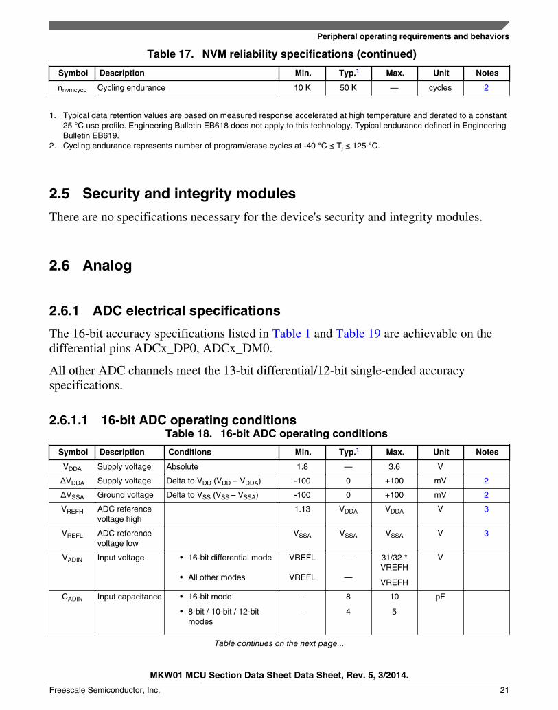
Table 17. NVM reliability specifications (continued)
Symbol Description Min. Typ.1 Max. Unit Notes
nnvmcycp Cycling endurance 10 K 50 K — cycles 2
1. Typical data retention values are based on measured response accelerated at high temperature and derated to a constant25 °C use profile. Engineering Bulletin EB618 does not apply to this technology. Typical endurance defined in EngineeringBulletin EB619.
2. Cycling endurance represents number of program/erase cycles at -40 °C ≤ Tj ≤ 125 °C.
2.5 Security and integrity modules
There are no specifications necessary for the device's security and integrity modules.
2.6 Analog
2.6.1 ADC electrical specifications
The 16-bit accuracy specifications listed in Table 1 and Table 19 are achievable on thedifferential pins ADCx_DP0, ADCx_DM0.
All other ADC channels meet the 13-bit differential/12-bit single-ended accuracyspecifications.
2.6.1.1 16-bit ADC operating conditionsTable 18. 16-bit ADC operating conditions
Symbol Description Conditions Min. Typ.1 Max. Unit Notes
VDDA Supply voltage Absolute 1.8 — 3.6 V
ΔVDDA Supply voltage Delta to VDD (VDD – VDDA) -100 0 +100 mV 2
ΔVSSA Ground voltage Delta to VSS (VSS – VSSA) -100 0 +100 mV 2
VREFH ADC referencevoltage high
1.13 VDDA VDDA V 3
VREFL ADC referencevoltage low
VSSA VSSA VSSA V 3
VADIN Input voltage • 16-bit differential mode
• All other modes
VREFL
VREFL
—
—
31/32 *VREFH
VREFH
V
CADIN Input capacitance • 16-bit mode
• 8-bit / 10-bit / 12-bitmodes
—
—
8
4
10
5
pF
Table continues on the next page...
Peripheral operating requirements and behaviors
MKW01 MCU Section Data Sheet Data Sheet, Rev. 5, 3/2014.
Freescale Semiconductor, Inc. 21

Table 18. 16-bit ADC operating conditions (continued)
Symbol Description Conditions Min. Typ.1 Max. Unit Notes
RADIN Input seriesresistance
— 2 5 kΩ
RAS Analog sourceresistance(external)
13-bit / 12-bit modes
fADCK < 4 MHz
—
—
5
kΩ
4
fADCK ADC conversionclock frequency
≤ 13-bit mode 1.0 — 18.0 MHz 5
fADCK ADC conversionclock frequency
16-bit mode 2.0 — 12.0 MHz 5
Crate ADC conversionrate
≤ 13-bit modes
No ADC hardware averaging
Continuous conversionsenabled, subsequentconversion time
20.000
—
818.330
Ksps
6
Crate ADC conversionrate
16-bit mode
No ADC hardware averaging
Continuous conversionsenabled, subsequentconversion time
37.037
—
461.467
Ksps
6
1. Typical values assume VDDA = 3.0 V, Temp = 25 °C, fADCK = 1.0 MHz, unless otherwise stated. Typical values are forreference only, and are not tested in production.
2. DC potential difference.3. For packages without dedicated VREFH and VREFL pins, VREFH is internally tied to VDDA, and VREFL is internally tied to
VSSA.4. This resistance is external to MCU. To achieve the best results, the analog source resistance must be kept as low as
possible. The results in this data sheet were derived from a system that had < 8 Ω analog source resistance. The RAS/CAStime constant should be kept to < 1 ns.
5. To use the maximum ADC conversion clock frequency, CFG2[ADHSC] must be set and CFG1[ADLPC] must be clear.6. For guidelines and examples of conversion rate calculation, download the ADC calculator tool.
Peripheral operating requirements and behaviors
MKW01 MCU Section Data Sheet Data Sheet, Rev. 5, 3/2014.
22 Freescale Semiconductor, Inc.

RAS
VASCAS
ZAS
VADIN
ZADIN
RADIN
RADIN
RADIN
RADIN
CADIN
Pad leakagedue toinput protection
INPUT PININPUT PIN
INPUT PIN
INPUT PIN
SIMPLIFIEDINPUT PIN EQUIVALENT
CIRCUITSIMPLIFIED
CHANNEL SELECTCIRCUIT ADC SAR
ENGINE
Figure 5. ADC input impedance equivalency diagram
2.6.1.2 16-bit ADC electrical characteristics
Table 19. 16-bit ADC characteristics (VREFH = VDDA, VREFL = VSSA)
Symbol Description Conditions1. Min. Typ.2 Max. Unit Notes
IDDA_ADC Supply current 0.215 — 1.7 mA 3
fADACK
ADCasynchronousclock source
• ADLPC = 1, ADHSC = 0
• ADLPC = 1, ADHSC = 1
• ADLPC = 0, ADHSC = 0
• ADLPC = 0, ADHSC = 1
1.2
2.4
3.0
4.4
2.4
4.0
5.2
6.2
3.9
6.1
7.3
9.5
MHz
MHz
MHz
MHz
tADACK = 1/fADACK
Sample Time See Reference Manual chapter for sample times
TUE Total unadjustederror
• 12-bit modes
• <12-bit modes
—
—
±4
±1.4
±6.8
±2.1
LSB4 5
DNL Differential non-linearity
• 12-bit modes
• <12-bit modes
—
—
±0.7
±0.2
–1.1 to+1.9
–0.3 to 0.5
LSB4 5
INL Integral non-linearity
• 12-bit modes
• <12-bit modes
—
—
±1.0
±0.5
–2.7 to+1.9
–0.7 to+0.5
LSB4 5
Table continues on the next page...
Peripheral operating requirements and behaviors
MKW01 MCU Section Data Sheet Data Sheet, Rev. 5, 3/2014.
Freescale Semiconductor, Inc. 23

Table 19. 16-bit ADC characteristics (VREFH = VDDA, VREFL = VSSA) (continued)
Symbol Description Conditions1. Min. Typ.2 Max. Unit Notes
EFS Full-scale error • 12-bit modes
• <12-bit modes
—
—
–4
–1.4
–5.4
–1.8
LSB4 VADIN =VDDA
5
EQ Quantizationerror
• 16-bit modes
• ≤13-bit modes
—
—
–1 to 0
—
—
±0.5
LSB4
ENOB Effective numberof bits
16-bit differential mode
• Avg = 32
• Avg = 4
16-bit single-ended mode
• Avg = 32
• Avg = 4
12.8
11.9
12.2
11.4
14.5
13.8
13.9
13.1
—
—
—
—
bits
bits
bits
bits
6
SINADSignal-to-noiseplus distortion
See ENOB6.02 × ENOB + 1.76 dB
THD Total harmonicdistortion
16-bit differential mode
• Avg = 32
16-bit single-ended mode
• Avg = 32
—
—
-94
-85
—
—
dB
dB
7
SFDR Spurious freedynamic range
16-bit differential mode
• Avg = 32
16-bit single-ended mode
• Avg = 32
82
78
95
90
—
—
dB
dB
7
EIL Input leakageerror
IIn × RAS mV IIn =leakagecurrent
(refer tothe MCU's
voltageand currentoperatingratings)
Temp sensorslope
Across the full temperaturerange of the device
1.55 1.62 1.69 mV/°C 8
VTEMP25 Temp sensorvoltage
25 °C 706 716 726 mV 8
1. All accuracy numbers assume the ADC is calibrated with VREFH = VDDA2. Typical values assume VDDA = 3.0 V, Temp = 25 °C, fADCK = 2.0 MHz unless otherwise stated. Typical values are for
reference only and are not tested in production.3. The ADC supply current depends on the ADC conversion clock speed, conversion rate and ADC_CFG1[ADLPC] (low
power). For lowest power operation, ADC_CFG1[ADLPC] must be set, the ADC_CFG2[ADHSC] bit must be clear with 1MHz ADC conversion clock speed.
4. 1 LSB = (VREFH - VREFL)/2N
Peripheral operating requirements and behaviors
MKW01 MCU Section Data Sheet Data Sheet, Rev. 5, 3/2014.
24 Freescale Semiconductor, Inc.

5. ADC conversion clock < 16 MHz, Max hardware averaging (AVGE = %1, AVGS = %11)6. Input data is 100 Hz sine wave. ADC conversion clock < 12 MHz.7. Input data is 1 kHz sine wave. ADC conversion clock < 12 MHz.8. ADC conversion clock < 3 MHz
Figure 6. Typical ENOB vs. ADC_CLK for 16-bit differential mode
Figure 7. Typical ENOB vs. ADC_CLK for 16-bit single-ended mode
Peripheral operating requirements and behaviors
MKW01 MCU Section Data Sheet Data Sheet, Rev. 5, 3/2014.
Freescale Semiconductor, Inc. 25

2.6.2 CMP and 6-bit DAC electrical specificationsTable 20. Comparator and 6-bit DAC electrical specifications
Symbol Description Min. Typ. Max. Unit
VDD Supply voltage 1.8 — 3.6 V
IDDHS Supply current, High-speed mode (EN=1, PMODE=1) — — 200 μA
IDDLS Supply current, low-speed mode (EN=1, PMODE=0) — — 20 μA
VAIN Analog input voltage VSS – 0.3 — VDD V
VAIO Analog input offset voltage — — 20 mV
VH Analog comparator hysteresis1
• CR0[HYSTCTR] = 00
• CR0[HYSTCTR] = 01
• CR0[HYSTCTR] = 10
• CR0[HYSTCTR] = 11
—
—
—
—
5
10
20
30
—
—
—
—
mV
mV
mV
mV
VCMPOh Output high VDD – 0.5 — — V
VCMPOl Output low — — 0.5 V
tDHS Propagation delay, high-speed mode (EN=1,PMODE=1)
20 50 200 ns
tDLS Propagation delay, low-speed mode (EN=1,PMODE=0)
80 250 600 ns
Analog comparator initialization delay2 — — 40 μs
IDAC6b 6-bit DAC current adder (enabled) — 7 — μA
INL 6-bit DAC integral non-linearity –0.5 — 0.5 LSB3
DNL 6-bit DAC differential non-linearity –0.3 — 0.3 LSB
1. Typical hysteresis is measured with input voltage range limited to 0.6 to VDD–0.6 V.2. Comparator initialization delay is defined as the time between software writes to change control inputs (Writes to
CMP_DACCR[DACEN], CMP_DACCR[VRSEL], CMP_DACCR[VOSEL], CMP_MUXCR[PSEL], andCMP_MUXCR[MSEL]) and the comparator output settling to a stable level.
3. 1 LSB = Vreference/64
Peripheral operating requirements and behaviors
MKW01 MCU Section Data Sheet Data Sheet, Rev. 5, 3/2014.
26 Freescale Semiconductor, Inc.

0.04
0.05
0.06
0.07
0.08P
Hys
tere
ris
(V)
00
01
10
HYSTCTR Setting
0
0.01
0.02
0.03
0.1 0.4 0.7 1 1.3 1.6 1.9 2.2 2.5 2.8 3.1
CM
10
11
Vin level (V)
Figure 8. Typical hysteresis vs. Vin level (VDD = 3.3 V, PMODE = 0)
Peripheral operating requirements and behaviors
MKW01 MCU Section Data Sheet Data Sheet, Rev. 5, 3/2014.
Freescale Semiconductor, Inc. 27

0 08
0.1
0.12
0.14
0.16
0.18P
Hys
tere
ris
(V)
00
01
10
HYSTCTR Setting
0
0.02
0.04
0.06
0.08
0.1 0.4 0.7 1 1.3 1.6 1.9 2.2 2.5 2.8 3.1
CMP 10
11
Vin level (V)
Figure 9. Typical hysteresis vs. Vin level (VDD = 3.3 V, PMODE = 1)
2.6.3 12-bit DAC electrical characteristics
2.6.3.1 12-bit DAC operating requirementsTable 21. 12-bit DAC operating requirements
Symbol Desciption Min. Max. Unit Notes
VDDA Supply voltage 1.8 3.6 V
VDACR Reference voltage 1.13 3.6 V 1
CL Output load capacitance — 100 pF 2
IL Output load current — 1 mA
1. The DAC reference can be selected to be VDDA or VREFH.2. A small load capacitance (47 pF) can improve the bandwidth performance of the DAC
Peripheral operating requirements and behaviors
MKW01 MCU Section Data Sheet Data Sheet, Rev. 5, 3/2014.
28 Freescale Semiconductor, Inc.

2.6.3.2 12-bit DAC operating behaviorsTable 22. 12-bit DAC operating behaviors
Symbol Description Min. Typ. Max. Unit Notes
IDDA_DACL
P
Supply current — low-power mode — — 250 μA
IDDA_DACH
P
Supply current — high-speed mode — — 900 μA
tDACLP Full-scale settling time (0x080 to 0xF7F) —low-power mode
— 100 200 μs 1
tDACHP Full-scale settling time (0x080 to 0xF7F) —high-power mode
— 15 30 μs 1
tCCDACLP Code-to-code settling time (0xBF8 to 0xC08)— low-power mode and high-speed mode
— 0.7 1 μs 1
Vdacoutl DAC output voltage range low — high-speedmode, no load, DAC set to 0x000
— — 100 mV
Vdacouth DAC output voltage range high — high-speed mode, no load, DAC set to 0xFFF
VDACR−100
— VDACR mV
INL Integral non-linearity error — high speedmode
— — ±8 LSB 2
DNL Differential non-linearity error — VDACR > 2V
— — ±1 LSB 3
DNL Differential non-linearity error — VDACR =VREF_OUT
— — ±1 LSB 4
VOFFSET Offset error — ±0.4 ±0.8 %FSR 5
EG Gain error — ±0.1 ±0.6 %FSR 5
PSRR Power supply rejection ratio, VDDA ≥ 2.4 V 60 — 90 dB
TCO Temperature coefficient offset voltage — 3.7 — μV/C 6
TGE Temperature coefficient gain error — 0.000421 — %FSR/C
Rop Output resistance (load = 3 kΩ) — — 250 Ω
SR Slew rate -80h→ F7Fh→ 80h
• High power (SPHP)
• Low power (SPLP)
1.2
0.05
1.7
0.12
—
—
V/μs
BW 3dB bandwidth
• High power (SPHP)
• Low power (SPLP)
550
40
—
—
—
—
kHz
1. Settling within ±1 LSB2. The INL is measured for 0 + 100 mV to VDACR −100 mV3. The DNL is measured for 0 + 100 mV to VDACR −100 mV4. The DNL is measured for 0 + 100 mV to VDACR −100 mV with VDDA > 2.4 V5. Calculated by a best fit curve from VSS + 100 mV to VDACR − 100 mV6. VDDA = 3.0 V, reference select set for VDDA (DACx_CO:DACRFS = 1), high power mode (DACx_C0:LPEN = 0), DAC set to
0x800, temperature range is across the full range of the device
Peripheral operating requirements and behaviors
MKW01 MCU Section Data Sheet Data Sheet, Rev. 5, 3/2014.
Freescale Semiconductor, Inc. 29

Figure 10. Typical INL error vs. digital code
Peripheral operating requirements and behaviors
MKW01 MCU Section Data Sheet Data Sheet, Rev. 5, 3/2014.
30 Freescale Semiconductor, Inc.

Figure 11. Offset at half scale vs. temperature
2.7 Timers
See General switching specifications.
2.8 Communication interfaces
2.8.1 SPI switching specifications
The Serial Peripheral Interface (SPI) provides a synchronous serial bus with master andslave operations. Many of the transfer attributes are programmable. The following tablesprovide timing characteristics for classic SPI timing modes. See the SPI chapter of thechip's Reference Manual for information about the modified transfer formats used forcommunicating with slower peripheral devices.
Peripheral operating requirements and behaviors
MKW01 MCU Section Data Sheet Data Sheet, Rev. 5, 3/2014.
Freescale Semiconductor, Inc. 31
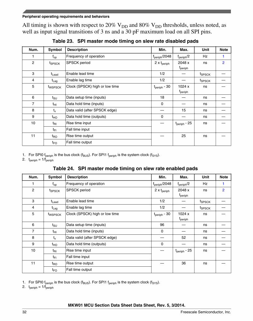
All timing is shown with respect to 20% VDD and 80% VDD thresholds, unless noted, aswell as input signal transitions of 3 ns and a 30 pF maximum load on all SPI pins.
Table 23. SPI master mode timing on slew rate disabled pads
Num. Symbol Description Min. Max. Unit Note
1 fop Frequency of operation fperiph/2048 fperiph/2 Hz 1
2 tSPSCK SPSCK period 2 x tperiph 2048 xtperiph
ns 2
3 tLead Enable lead time 1/2 — tSPSCK —
4 tLag Enable lag time 1/2 — tSPSCK —
5 tWSPSCK Clock (SPSCK) high or low time tperiph - 30 1024 xtperiph
ns —
6 tSU Data setup time (inputs) 18 — ns —
7 tHI Data hold time (inputs) 0 — ns —
8 tv Data valid (after SPSCK edge) — 15 ns —
9 tHO Data hold time (outputs) 0 — ns —
10 tRI Rise time input — tperiph - 25 ns —
tFI Fall time input
11 tRO Rise time output — 25 ns —
tFO Fall time output
1. For SPI0 fperiph is the bus clock (fBUS). For SPI1 fperiph is the system clock (fSYS).2. tperiph = 1/fperiph
Table 24. SPI master mode timing on slew rate enabled pads
Num. Symbol Description Min. Max. Unit Note
1 fop Frequency of operation fperiph/2048 fperiph/2 Hz 1
2 tSPSCK SPSCK period 2 x tperiph 2048 xtperiph
ns 2
3 tLead Enable lead time 1/2 — tSPSCK —
4 tLag Enable lag time 1/2 — tSPSCK —
5 tWSPSCK Clock (SPSCK) high or low time tperiph - 30 1024 xtperiph
ns —
6 tSU Data setup time (inputs) 96 — ns —
7 tHI Data hold time (inputs) 0 — ns —
8 tv Data valid (after SPSCK edge) — 52 ns —
9 tHO Data hold time (outputs) 0 — ns —
10 tRI Rise time input — tperiph - 25 ns —
tFI Fall time input
11 tRO Rise time output — 36 ns —
tFO Fall time output
1. For SPI0 fperiph is the bus clock (fBUS). For SPI1 fperiph is the system clock (fSYS).2. tperiph = 1/fperiph
Peripheral operating requirements and behaviors
MKW01 MCU Section Data Sheet Data Sheet, Rev. 5, 3/2014.
32 Freescale Semiconductor, Inc.

(OUTPUT)
2
8
6 7
MSB IN 2
LSB IN
MSB OUT 2 LSB OUT
9
5
5
3
(CPOL=0)
411
1110
10
SPSCK
SPSCK(CPOL=1)
2. LSBF = 0. For LSBF = 1, bit order is LSB, bit 1, ..., bit 6, MSB.1. If configured as an output.
SS 1
(OUTPUT)
(OUTPUT)
MOSI(OUTPUT)
MISO(INPUT)
BIT 6 . . . 1
BIT 6 . . . 1
Figure 12. SPI master mode timing (CPHA = 0)
<<CLASSIFICATION>> <<NDA MESSAGE>>
38
2
6 7
MSB IN 2
BIT 6 . . . 1 MASTER MSB OUT 2 MASTER LSB OUT
55
8
10 11
PORT DATA PORT DATA
3 10 11 4
1.If configured as output 2. LSBF = 0. For LSBF = 1, bit order is LSB, bit 1, ..., bit 6, MSB.
9
(OUTPUT)
(CPOL=0)SPSCK
SPSCK(CPOL=1)
SS 1
(OUTPUT)
(OUTPUT)
MOSI(OUTPUT)
MISO(INPUT) LSB INBIT 6 . . . 1
Figure 13. SPI master mode timing (CPHA = 1)
Table 25. SPI slave mode timing on slew rate disabled pads
Num. Symbol Description Min. Max. Unit Note
1 fop Frequency of operation 0 fperiph/4 Hz 1
2 tSPSCK SPSCK period 4 x tperiph — ns 2
3 tLead Enable lead time 1 — tperiph —
4 tLag Enable lag time 1 — tperiph —
5 tWSPSCK Clock (SPSCK) high or low time tperiph - 30 — ns —
Table continues on the next page...
Peripheral operating requirements and behaviors
MKW01 MCU Section Data Sheet Data Sheet, Rev. 5, 3/2014.
Freescale Semiconductor, Inc. 33

Table 25. SPI slave mode timing on slew rate disabled pads (continued)
Num. Symbol Description Min. Max. Unit Note
6 tSU Data setup time (inputs) 2.5 — ns —
7 tHI Data hold time (inputs) 3.5 — ns —
8 ta Slave access time — tperiph ns 3
9 tdis Slave MISO disable time — tperiph ns 4
10 tv Data valid (after SPSCK edge) — 31 ns —
11 tHO Data hold time (outputs) 0 — ns —
12 tRI Rise time input — tperiph - 25 ns —
tFI Fall time input
13 tRO Rise time output — 25 ns —
tFO Fall time output
1. For SPI0 fperiph is the bus clock (fBUS). For SPI1 fperiph is the system clock (fSYS).2. tperiph = 1/fperiph3. Time to data active from high-impedance state4. Hold time to high-impedance state
Table 26. SPI slave mode timing on slew rate enabled pads
Num. Symbol Description Min. Max. Unit Note
1 fop Frequency of operation 0 fperiph/4 Hz 1
2 tSPSCK SPSCK period 4 x tperiph — ns 2
3 tLead Enable lead time 1 — tperiph —
4 tLag Enable lag time 1 — tperiph —
5 tWSPSCK Clock (SPSCK) high or low time tperiph - 30 — ns —
6 tSU Data setup time (inputs) 2 — ns —
7 tHI Data hold time (inputs) 7 — ns —
8 ta Slave access time — tperiph ns 3
9 tdis Slave MISO disable time — tperiph ns 4
10 tv Data valid (after SPSCK edge) — 122 ns —
11 tHO Data hold time (outputs) 0 — ns —
12 tRI Rise time input — tperiph - 25 ns —
tFI Fall time input
13 tRO Rise time output — 36 ns —
tFO Fall time output
1. For SPI0 fperiph is the bus clock (fBUS). For SPI1 fperiph is the system clock (fSYS).2. tperiph = 1/fperiph3. Time to data active from high-impedance state4. Hold time to high-impedance state
Peripheral operating requirements and behaviors
MKW01 MCU Section Data Sheet Data Sheet, Rev. 5, 3/2014.
34 Freescale Semiconductor, Inc.
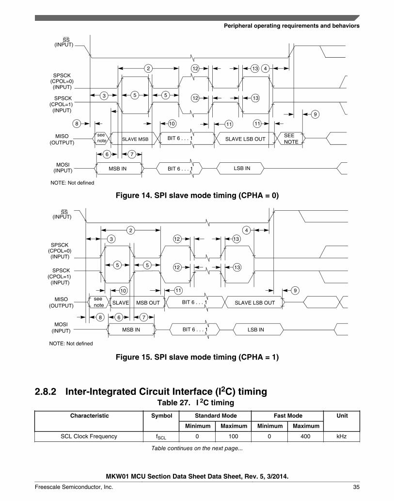
2
10
6 7
MSB IN
BIT 6 . . . 1 SLAVE MSB SLAVE LSB OUT
11
553
8
4
13
NOTE: Not defined
12
12
11
SEE NOTE
13
9
see note
(INPUT)
(CPOL=0)SPSCK
SPSCK(CPOL=1)
SS
(INPUT)
(INPUT)
MOSI(INPUT)
MISO(OUTPUT)
LSB INBIT 6 . . . 1
Figure 14. SPI slave mode timing (CPHA = 0)
2
6 7
MSB IN
BIT 6 . . . 1 MSB OUT SLAVE LSB OUT
55
10
12 13
3 12 13
4
SLAVE
8
9
see note
(INPUT)
(CPOL=0)SPSCK
SPSCK(CPOL=1)
SS
(INPUT)
(INPUT)
MOSI(INPUT)
MISO(OUTPUT)
NOTE: Not defined
11
LSB INBIT 6 . . . 1
Figure 15. SPI slave mode timing (CPHA = 1)
2.8.2 Inter-Integrated Circuit Interface (I2C) timingTable 27. I 2C timing
Characteristic Symbol Standard Mode Fast Mode Unit
Minimum Maximum Minimum Maximum
SCL Clock Frequency fSCL 0 100 0 400 kHz
Table continues on the next page...
Peripheral operating requirements and behaviors
MKW01 MCU Section Data Sheet Data Sheet, Rev. 5, 3/2014.
Freescale Semiconductor, Inc. 35

Table 27. I 2C timing (continued)
Characteristic Symbol Standard Mode Fast Mode Unit
Minimum Maximum Minimum Maximum
Hold time (repeated) START condition.After this period, the first clock pulse is
generated.
tHD; STA 4 — 0.6 — µs
LOW period of the SCL clock tLOW 4.7 — 1.3 — µs
HIGH period of the SCL clock tHIGH 4 — 0.6 — µs
Set-up time for a repeated STARTcondition
tSU; STA 4.7 — 0.6 — µs
Data hold time for I2C bus devices tHD; DAT 01 3.452 03 0.91 µs
Data set-up time tSU; DAT 2504 — 1002, 5 — ns
Rise time of SDA and SCL signals tr — 1000 20 +0.1Cb6 300 ns
Fall time of SDA and SCL signals tf — 300 20 +0.1Cb5 300 ns
Set-up time for STOP condition tSU; STO 4 — 0.6 — µs
Bus free time between STOP andSTART condition
tBUF 4.7 — 1.3 — µs
Pulse width of spikes that must besuppressed by the input filter
tSP N/A N/A 0 50 ns
1. The master mode I2C deasserts ACK of an address byte simultaneously with the falling edge of SCL. If no slavesacknowledge this address byte, then a negative hold time can result, depending on the edge rates of the SDA and SCLlines.
2. The maximum tHD; DAT must be met only if the device does not stretch the LOW period (tLOW) of the SCL signal.3. Input signal Slew = 10 ns and Output Load = 50 pF4. Set-up time in slave-transmitter mode is 1 IPBus clock period, if the TX FIFO is empty.5. A Fast mode I2C bus device can be used in a Standard mode I2C bus system, but the requirement tSU; DAT ≥ 250 ns must
then be met. This is automatically the case if the device does not stretch the LOW period of the SCL signal. If such adevice does stretch the LOW period of the SCL signal, then it must output the next data bit to the SDA line trmax + tSU; DAT= 1000 + 250 = 1250 ns (according to the Standard mode I2C bus specification) before the SCL line is released.
6. Cb = total capacitance of the one bus line in pF.
SDA
SCL
tHD; STAtHD; DAT
tLOW
tSU; DAT
tHIGH
tSU; STASR P SS
tHD; STA tSP
tSU; STO
tBUFtf trtf
tr
Figure 16. Timing definition for fast and standard mode devices on the I2C bus
2.8.3 UART
See General switching specifications.
Peripheral operating requirements and behaviors
MKW01 MCU Section Data Sheet Data Sheet, Rev. 5, 3/2014.
36 Freescale Semiconductor, Inc.

2.9 Human-machine interfaces (HMI)
2.9.1 TSI electrical specificationsTable 28. TSI electrical specifications
Symbol Description Min. Typ. Max. Unit
TSI_RUNF Fixed power consumption in run mode — 100 — µA
TSI_RUNV Variable power consumption in run mode(depends on oscillator's current selection)
1.0 — 128 µA
TSI_EN Power consumption in enable mode — 100 — µA
TSI_DIS Power consumption in disable mode — 1.2 — µA
TSI_TEN TSI analog enable time — 66 — µs
TSI_CREF TSI reference capacitor — 1.0 — pF
TSI_DVOLT Voltage variation of VP & VM around nominalvalues
0.19 — 1.03 V
Peripheral operating requirements and behaviors
MKW01 MCU Section Data Sheet Data Sheet, Rev. 5, 3/2014.
Freescale Semiconductor, Inc. 37

MKW01Z128 Advance Information, Rev. 5
28 Freescale Semiconductor
10 Mechanical Drawings
Figure 8. Mechanical Drawing (1 of 2)
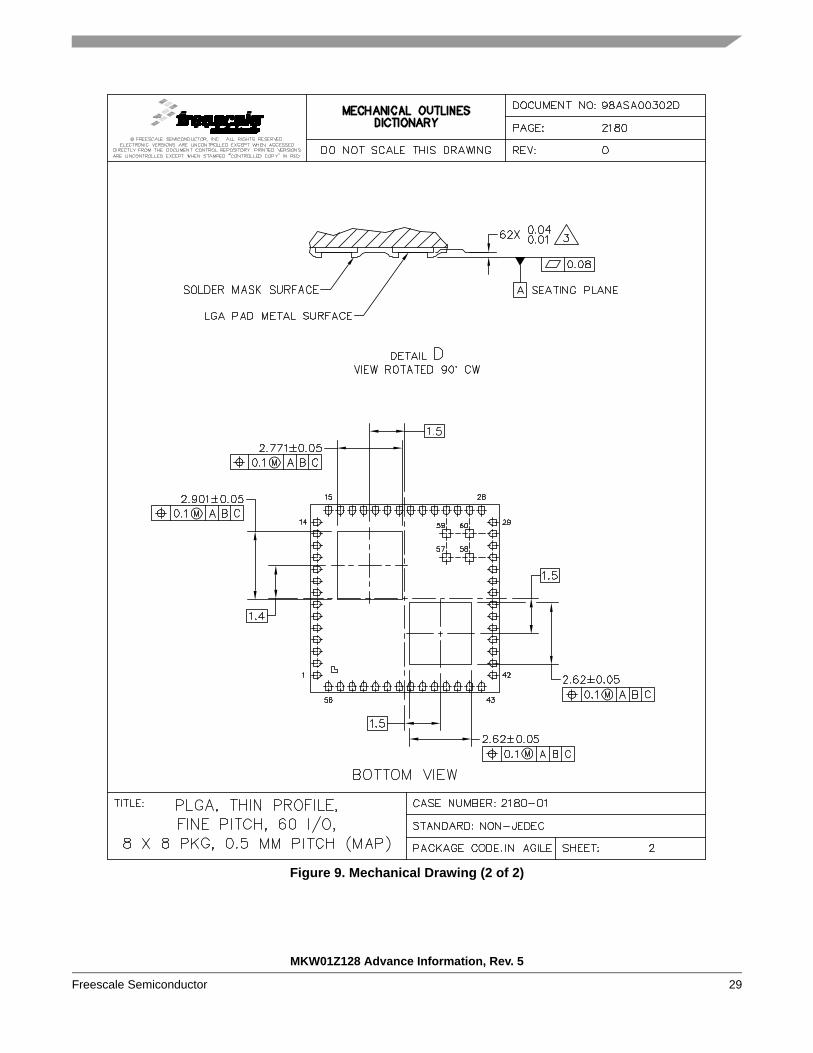
MKW01Z128 Advance Information, Rev. 5
Freescale Semiconductor 29
Figure 9. Mechanical Drawing (2 of 2)

Document Number: MKW01Z128Rev. 5
How to Reach Us:
Home Page:freescale.com
Web Support:freescale.com/support
Information in this document is provided solely to enable system and software implementers to use
Freescale products. There are no express or implied copyright licenses granted hereunder to design
or fabricate any integrated circuits based on the information in this document.
Freescale reserves the right to make changes without further notice to any products herein.
Freescale makes no warranty, representation, or guarantee regarding the suitability of its products
for any particular purpose, nor does Freescale assume any liability arising out of the application or
use of any product or circuit, and specifically disclaims any and all liability, including without limitation
consequential or incidental damages. “Typical” parameters that may be provided in Freescale data
sheets and/or specifications can and do vary in different applications, and actual performance may
vary over time. All operating parameters, including “typicals,” must be validated for each customer
application by customer’s technical experts. Freescale does not convey any license under its patent
rights nor the rights of others. Freescale sells products pursuant to standard terms and conditions of
sale, which can be found at the following address: freescale.com/SalesTermsandConditions.
Freescale, the Freescale logo, AltiVec, CodeWarrior, ColdFire, ColdFire+,Energy Efficient Solutions
logo, PowerQUICC, QorIQ, StarCore, Symphony, and VortiQa are trademarks of Freescale
Semiconductor, Inc., Reg. U.S. Pat. & Tm. Off. CoreNet, Layerscape, QorIQ Qonverge, QUICC
Engine, Tower, and Xtrinsic are trademarks of Freescale Semiconductor, Inc. All other product or
service names are the property of their respective owners. ARM and Cortex are registered
trademarks of ARM Limited. ARMnnn is the trademark of ARM Limited.
© 2014 Freescale Semiconductor, Inc.


![DESIGN AND ANALYSIS OF EFFICIENT PHASE LOCKED LOOP … · Phase Locked Loop (PLL) mainly for synchronization, clock synthesis, skew and jitter reduction [5]. Phase locked loops find](https://static.fdocuments.us/doc/165x107/5e9d540ca2a49a4e746bfacd/design-and-analysis-of-efficient-phase-locked-loop-phase-locked-loop-pll-mainly.jpg)


