MIRSI: a Mid-InfraRed Spectrometer and Imager - Harvard
11
MIRSI: a Mid-InfraRed Spectrometer and Imager Lynne K. Deutsch *a,b , Joseph L. Hora b , Joseph D. Adams a , Marc Kassis a a Boston University, b Harvard-Smithsonian Center for Astrophysics ABSTRACT MIRSI (Mid-InfraRed Spectrometer and Imager) is a mid-infrared camera system recently completed at Boston University that has both spectroscopic and imaging capabilities. MIRSI is uniquely suited for studies of young stellar objects and star formation, planetary and protoplanetary nebulae, starburst galaxies, and solar system objects such as planets, asteroids, and comets. The camera utilizes a new 320 x 240 Si:As Impurity Band Conduction (IBC) array developed for ground-based astronomy by Raytheon/SBRC. For observations at the Infrared Telescope Facility (IRTF), MIRSI offers a large field of view (1.6 arcmin x 1.2 arcmin) with a pixel scale of 0.3 arcsec, diffraction-limited spatial resolution, complete spectral coverage over the 8-14 μm and 17-26 μm atmospheric windows for both imaging (discrete filters and circular variable filter) and spectroscopy (10 and 20 μm grisms), and high sensitivity (expected one-sigma point source sensitivities of 5 and 20 mJy at 10 and 20 μm, respectively, for on-source integration time of 30 seconds). MIRSI successfully achieved first light at the Mt. Lemmon Observing Facility (MLOF) in December 2001, and will have its first observing run at the IRTF in November 2002. We present details of the system hardware and software and results from first light observations. Keywords: infrared astronomy, infrared arrays, mid-infrared instrumentation 1. INTRODUCTION The MIRSI 1,2 system (http://mirador.bu.edu/mirsi/mirsi.html ) was designed for the study of a number of astrophysical phenomena that require thermal infrared observations in order to penetrate their warm, dusty environments. The system has the capability to acquire both spectra and high-resolution, multi-wavelength images. This makes it possible to unambiguously correlate the spatial and spectral features observed in astrophysical sources and thereby reveal the key physical and chemical processes at work. The MIRSI instrument concept had to satisfy several requirements to meet our scientific goals: • Operation over the 8-14 μm and 17-26 μm wavelength ranges. • Large field of view. • Diffraction-limited imaging. • In imaging mode, provide spectral resolution of up to 1% bandwidth for imaging of spectral features. • In spectroscopic mode, provide resolution of ~200, sufficient to resolve broad spectral features and detect narrow spectral features. • Quick and easy selection of observing mode, with the flexibility to change observing parameters in real time. • Efficient, high throughput optics. • Telescope control capable of commanding offset, chop, and beamswitch. • Simple, real-time data reduction and quick-look capability. Our design addresses each of these requirements. The camera system is based on a Raytheon/SBRC Si:As IBC CRC774 array with 320 x 240 pixels and a spectral range of 2-28 μm. The array is designed for high-flux applications and is read out through 16 parallel readout lines. The system is housed in a cryostat containing LN 2 and LHe reservoirs attached to an outer LN 2 radiation shield and an inner LHe shield, respectively. The main camera characteristics are summarized in * [email protected] ; phone; 60 Garden Street, MS-65, Cambridge, MA 02138-1516
Transcript of MIRSI: a Mid-InfraRed Spectrometer and Imager - Harvard

MIRSI: a Mid-InfraRed Spectrometer and Imager
Lynne K. Deutsch*a,b, Joseph L. Horab, Joseph D. Adamsa, Marc Kassisa
aBoston University, bHarvard-Smithsonian Center for Astrophysics
ABSTRACT MIRSI (Mid-InfraRed Spectrometer and Imager) is a mid-infrared camera system recently completed at Boston University that has both spectroscopic and imaging capabil ities. MIRSI is uniquely suited for studies of young stellar objects and star formation, planetary and protoplanetary nebulae, starburst galaxies, and solar system objects such as planets, asteroids, and comets. The camera utilizes a new 320 x 240 Si:As Impurity Band Conduction (IBC) array developed for ground-based astronomy by Raytheon/SBRC. For observations at the Infrared Telescope Facili ty (IRTF), MIRSI offers a large field of view (1.6 arcmin x 1.2 arcmin) with a pixel scale of 0.3 arcsec, diffraction-limited spatial resolution, complete spectral coverage over the 8-14 µm and 17-26 µm atmospheric windows for both imaging (discrete filters and circular variable filter) and spectroscopy (10 and 20 µm grisms), and high sensitivity (expected one-sigma point source sensitivities of 5 and 20 mJy at 10 and 20 µm, respectively, for on-source integration time of 30 seconds). MIRSI successfully achieved first light at the Mt. Lemmon Observing Facili ty (MLOF) in December 2001, and will have its first observing run at the IRTF in November 2002. We present details of the system hardware and software and results from first light observations. Keywords: infrared astronomy, infrared arrays, mid-infrared instrumentation
1. INTRODUCTION The MIRSI1,2 system (http://mirador.bu.edu/mirsi/mirsi.html) was designed for the study of a number of astrophysical phenomena that require thermal infrared observations in order to penetrate their warm, dusty environments. The system has the capability to acquire both spectra and high-resolution, multi-wavelength images. This makes it possible to unambiguously correlate the spatial and spectral features observed in astrophysical sources and thereby reveal the key physical and chemical processes at work. The MIRSI instrument concept had to satisfy several requirements to meet our scientific goals:
• Operation over the 8-14 µm and 17-26 µm wavelength ranges. • Large field of view. • Diffraction-limited imaging. • In imaging mode, provide spectral resolution of up to 1% bandwidth for imaging of spectral features. • In spectroscopic mode, provide resolution of ~200, sufficient to resolve broad spectral features and detect
narrow spectral features. • Quick and easy selection of observing mode, with the flexibility to change observing parameters in real time. • Efficient, high throughput optics. • Telescope control capable of commanding offset, chop, and beamswitch. • Simple, real-time data reduction and quick-look capability.
Our design addresses each of these requirements. The camera system is based on a Raytheon/SBRC Si:As IBC CRC774 array with 320 x 240 pixels and a spectral range of 2-28 µm. The array is designed for high-flux applications and is read out through 16 parallel readout lines. The system is housed in a cryostat containing LN2 and LHe reservoirs attached to an outer LN2 radiation shield and an inner LHe shield, respectively. The main camera characteristics are summarized in
* [email protected]; phone; 60 Garden Street, MS-65, Cambridge, MA 02138-1516

Table 1, and the array characteristics are given in Table 2. Details of the optical system, dewar, electronics, computer control, system integration and testing follow. We expect to observe regularly at the IRTF through an arrangement that makes MIRSI available for collaborative observational programs on that telescope. We expect to use MIRSI on other telescopes as well .
Table 1. Summary of MIRSI characteristics
Spectral Range 2-28 µm Pixel Scale 0.3 arcsec/pixel
Field of View 96 x 72 arcsec Spectroscopic Resolution 100-200 Estimated NEFD at 10 µm 3.4 x 10⁻³ Jy Hz-1/2 Estimated NEFD at 20 µm 7.5 x 10⁻³ Jy Hz-1/2
Optics Reflective
Table 2. Summary of array characteristics.
2. MECHANICAL DESIGN 2.1 MIRSI Dewar design The MIRSI dewar design was developed under our direction at IR Labs and consists of two main sections: a standard 12-inch cylindrical case that contains the LN2 and LHe cryogen cans and fill tubes, and a rectangular box that holds the array, optics, and filters (see Figure 1). The camera is designed to be an up-looking system, in order to minimize the number of reflections from warm surfaces that add to the emissivity and reduce sensitivity. This is the nominal configuration for the IRTF and other telescopes where we will mount directly at the Cassegrain focus. In order to minimize cost, the design uses a standard case and cryogen can sizes; however, the fil l tubes are mounted on the “side” rather than the end of the cylinder so that the dewar lies with its long axis horizontally for fill ing and nominal operation. IR Labs has built other systems using this configuration, so the design had been proven to work with performance comparable to their normal “ top-fill ” systems. We find that the MIRSI dewar performs as expected in this configuration, with the added benefit that the fil l ports are displaced far enough from the telescope that we can fill the dewar without dismounting.
Number of pixels 320 x 240 Pixel pitch 50 µm Material Si:As
Technology IBC Operating temperature range 6-12 K
Peak quantum efficiency > 40% Dark current
��������� -/s Frame Rates ���� ����
Number of outputs 16 Well depth 3 x 10⁷ e- or
1 x 10⁷ e- Read noise < 2800 e- or
< 1000 e- Nonlinearity ������� Operability 99.5%
Power dissipation ~140 mW
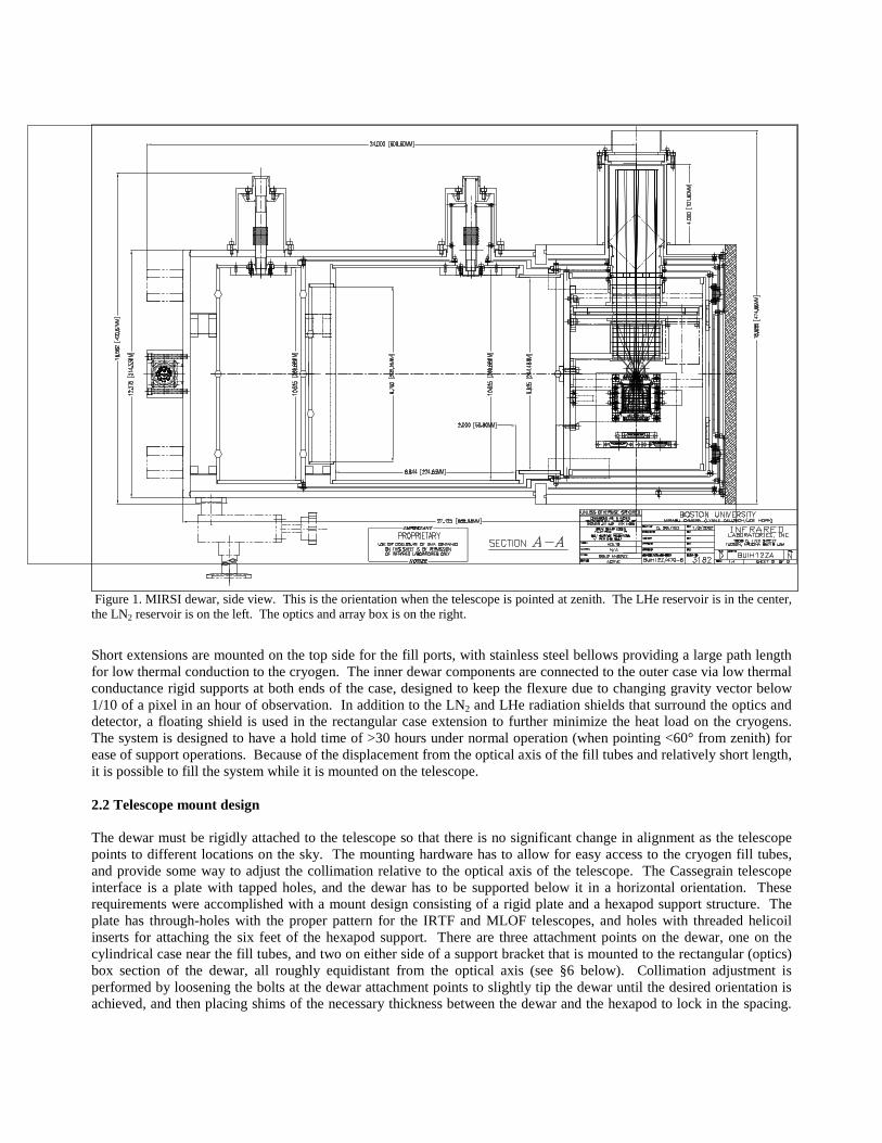
Figure 1. MIRSI dewar, side view. This is the orientation when the telescope is pointed at zenith. The LHe reservoir is in the center, the LN2 reservoir is on the left. The optics and array box is on the right.
Short extensions are mounted on the top side for the fil l ports, with stainless steel bellows providing a large path length for low thermal conduction to the cryogen. The inner dewar components are connected to the outer case via low thermal conductance rigid supports at both ends of the case, designed to keep the flexure due to changing gravity vector below 1/10 of a pixel in an hour of observation. In addition to the LN2 and LHe radiation shields that surround the optics and detector, a floating shield is used in the rectangular case extension to further minimize the heat load on the cryogens. The system is designed to have a hold time of >30 hours under normal operation (when pointing <60° from zenith) for ease of support operations. Because of the displacement from the optical axis of the fill tubes and relatively short length, it is possible to fill the system while it is mounted on the telescope. 2.2 Telescope mount design The dewar must be rigidly attached to the telescope so that there is no significant change in alignment as the telescope points to different locations on the sky. The mounting hardware has to allow for easy access to the cryogen fill tubes, and provide some way to adjust the coll imation relative to the optical axis of the telescope. The Cassegrain telescope interface is a plate with tapped holes, and the dewar has to be supported below it in a horizontal orientation. These requirements were accomplished with a mount design consisting of a rigid plate and a hexapod support structure. The plate has through-holes with the proper pattern for the IRTF and MLOF telescopes, and holes with threaded helicoil inserts for attaching the six feet of the hexapod support. There are three attachment points on the dewar, one on the cylindrical case near the fill tubes, and two on either side of a support bracket that is mounted to the rectangular (optics) box section of the dewar, all roughly equidistant from the optical axis (see §6 below). Coll imation adjustment is performed by loosening the bolts at the dewar attachment points to slightly tip the dewar until the desired orientation is achieved, and then placing shims of the necessary thickness between the dewar and the hexapod to lock in the spacing.

An L-shaped bracket holding the detector electronics box is bolted to the end of the optics box section and to the camera interface plate.
3. OPTICAL DESIGN Light from the telescope passes through the dewar window and short snout to the telescope focus at the surface of an aperture wheel (a field stop for the camera mode or slit in the spectroscopic mode). After passing through the wheel opening, the beam reflects off a folding flat and then an off-axis parabolic collimator mirror and is directed towards the pupil stop. Two filter wheels are located near the pupil. The one nearest to the pupil holds the CVF, grisms, and discrete-filter blockers. The size of the pupil (nominally 5mm at the IRTF) has been minimized in the optical design to provide adequate spectral resolution when using the CVF. This also leads to a compact size for the relatively large field being imaged. The second wheel holds broad- and narrow-band filters and CVF blockers. The filters are tilted in these wheels with respect to the incoming beam to avoid ghost images.
Figure 2. MIRSI dewar, end view, showing optics. The optical ray trace is shown entering the dewar from the top, with the thick line representing the central ray. After passing through the pupil, the light reflects off the two off-axis aspheric camera mirrors and is reimaged on the detector array at the desired image scale. At the IRTF, this is 0.3 � ������������ ������� ���������� ����������� � �!#" $&%('�) *,+.-/1032�/�4576scale properly samples diffraction- 8�9;:<9�=?>7@A9;:<B7C�>�DE9;F,=1G>IHKJLBMF@,NJ O(PRQTS�UVXW(QZYM[]\_^`aW�b�b -axis design produces some
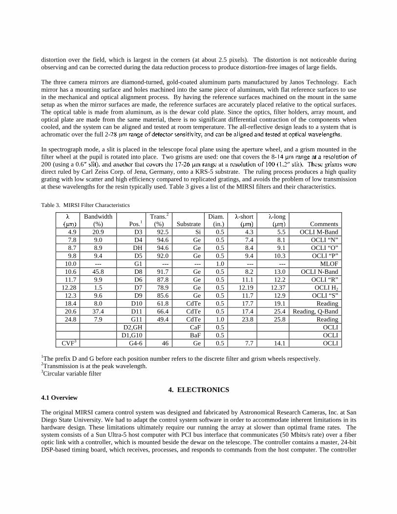
distortion over the field, which is largest in the corners (at about 2.5 pixels). The distortion is not noticeable during observing and can be corrected during the data reduction process to produce distortion-free images of large fields. The three camera mirrors are diamond-turned, gold-coated aluminum parts manufactured by Janos Technology. Each mirror has a mounting surface and holes machined into the same piece of aluminum, with flat reference surfaces to use in the mechanical and optical alignment process. By having the reference surfaces machined on the mount in the same setup as when the mirror surfaces are made, the reference surfaces are accurately placed relative to the optical surfaces. The optical table is made from aluminum, as is the dewar cold plate. Since the optics, filter holders, array mount, and optical plate are made from the same material, there is no significant differential contraction of the components when cooled, and the system can be aligned and tested at room temperature. The all-reflective design leads to a system that is achromatic over the full 2- ����� ����� ����� ������������������������� !�� #"� $�&%('���)���*��,+����*-. &�/)���0��)�1��������������2��3 �� .�*��-�41�*" �*-.�5 �/�.6���7 In spectrograph mode, a slit is placed in the telescope focal plane using the aperture wheel, and a grism mounted in the filter wheel at the pupil is rotated into place. Two grisms are used: one that covers the 8- 8:9<; =?>@�A)B�C,@�DE@F>CHG�I�J#KLD�M&ILANI�O200 (using a 0.6 P QSR&T#UWVX�Y�Z�[\Y�Z�]�U.^)_�`�U&^�Y�Uba*]/c)_�`SQ�UW^)_Nd�e - f�gNh ikjl�m)n�opl�qrlFjoHs�t�u#v�q�w.t�mNt)xzy�{ {\|�y�} ~���sSu&w#qW��}\�E�)oHs�o1n/jwWs�iNs��,o�j�odirect ruled by Carl Zeiss Corp. of Jena, Germany, onto a KRS-5 substrate. The ruling process produces a high quality grating with low scatter and high efficiency compared to replicated gratings, and avoids the problem of low transmission at these wavelengths for the resin typically used. Table 3 gives a list of the MIRSI filters and their characteristics.
Table 3. MIRSI Filter Characteristics � ��L� �$�
Bandwidth
(%)
Pos.1 Trans.2
(%)
Substrate Diam.
(in.)
�-short ���L���$�
�-long ��L���$�
Comments 4.9 20.9 D3 92.5 Si 0.5 4.3 5.5 OCLI M-Band 7.8 9.0 D4 94.6 Ge 0.5 7.4 8.1 OCLI “N” 8.7 8.9 DH 94.6 Ge 0.5 8.4 9.1 OCLI “O” 9.8 9.4 D5 92.0 Ge 0.5 9.4 10.3 OCLI “P”
10.0 --- G1 --- --- 1.0 --- --- MLOF 10.6 45.8 D8 91.7 Ge 0.5 8.2 13.0 OCLI N-Band 11.7 9.9 D6 87.8 Ge 0.5 11.1 12.2 OCLI “R”
12.28 1.5 D7 78.9 Ge 0.5 12.19 12.37 OCLI H2 12.3 9.6 D9 85.6 Ge 0.5 11.7 12.9 OCLI “S” 18.4 8.0 D10 61.8 CdTe 0.5 17.7 19.1 Reading 20.6 37.4 D11 66.4 CdTe 0.5 17.4 25.4 Reading, Q-Band 24.8 7.9 G11 49.4 CdTe 1.0 23.8 25.8 Reading
D2,GH CaF 0.5 OCLI D1,G10 BaF 0.5 OCLI
CVF3 G4-6 46 Ge 0.5 7.7 14.1 OCLI 1The prefix D and G before each position number refers to the discrete filter and grism wheels respectively. 2Transmission is at the peak wavelength. 3Circular variable filter
4. ELECTRONICS 4.1 Overview The original MIRSI camera control system was designed and fabricated by Astronomical Research Cameras, Inc. at San Diego State University. We had to adapt the control system software in order to accommodate inherent limitations in its hardware design. These limitations ultimately require our running the array at slower than optimal frame rates. The system consists of a Sun Ultra-5 host computer with PCI bus interface that communicates (50 Mbits/s rate) over a fiber optic link with a controller, which is mounted beside the dewar on the telescope. The controller contains a master, 24-bit DSP-based timing board, which receives, processes, and responds to commands from the host computer. The controller

also contains two driver boards for setting and driving the detector bias and clock voltages, respectively. Four DSP coadder boards containing four channels each read and amplify the array output, handle A/D conversion, and initiall y coadd and store images in real time using several SRAM memory chips (about 1 MB total on each board). The timing, clock driver, coadder, and a chop driver interface boards are linked through a VME backplane with power control board and external master power supply. The timing board sends images acquired by the coadder boards to the PCI interface board in the host computer. The user interface software reads images in PCI board memory and writes them to hard disk in standard FITS format. 4.2 PCI interface A PCI board on the 32-bit Sun host computer bus contains a Motorola 56301 24-bit DSP with PCI interface. The DSP communicates with the camera controller through two fiber optic interfaces, which receive and transmit data, respectively. Boot code stored in an onboard EEPROM chip controls the PCI DSP. The board contains an 18 kB FIFO buffer between the DSP and the board's fiber optic receive port. The PCI board also holds a 72 MB bank of dynamic RAM space for storing additional image data from the controller. The DSP PCI interface contains a small FIFO buffer that holds commands written from the host bus. The 32-bit host commands are divided and processed by the DSP as two 16-bit words. The DSP itself contains 4096 × 24-bit of internal program memory, and additional internal X:RAM and Y:RAM memory pages of 2048 × 24-bit each. 4.3 Timing and clock driver boards The timing board contains a fiber optic interface for communication with the host computer PCI board. A Motorola 24-bit DSP 56002 controls the timing board. Assembly code is created and compiled on the host machine, then downloaded into DSP memory through the PCI interface. Primary tasks include processing 24-bit commands from the host computer. Individual commands can be sent manually from the Graphical User Interface (GUI). Typically, sets of DSP commands are sent automatically by the host software on a given high level user command. The array power-on sequence loads voltage levels from internal memory into the DACs, then enables the DAC outputs to bring up the DC bias voltages and clocks. Finally, the power on-sequence puts the camera into continuous reset mode. Between idle array frame cycles, the timing software checks for a new command for the host computer, and, if present, executes the new command. The two clock driver boards each contain twelve 12-bit, 4-output DACs. One of each set of two DAC outputs is selected with an analog switch. This provides either switching clock voltages or a DC bias voltage for each array pin. The clock driver board uses a total of 18 voltage lines, while the bias board uses a total of 23 voltage lines. The switch-selected DAC outputs are buffered and sent to the dewar; the clock lines are individually shielded. Within the dewar, shielded clock and bias lines are carried through the radiation shields and thermally attached to the 77 K shield. The lines are allowed to thermally float from the 77 K shield to the detector board in order to increase the heat path length, and thereby decrease heat load on the helium reservoir. The timing board also controls important signal bits, such as the gains (or input ranges) on the coadder board A/Ds (0 → -5 V or 0 → -10 V). Typically, the high A/D gain (0 → -5 V) is used. Subsequent to control system delivery, we added the use of two DSP pins (H4 and H5) as utility bits that toggle chop signal and nod signal bits, respectively. The chop and nod bits are sent to a chop driver interface board containing buffers and fiber optic output interface. The optical chop/nod levels are then carried over fiber optic cables to an external chop driver box. This box contains an externally powered circuit that converts the optical signals to TTL level signals, which are sent to the telescope control system through BNC cables. At IRTF, MIRSI uses high level software on the host computer to control nod status over the network. 4.4 Signals and coadder boards The sixteen array output signals are electrically shielded and carried through the radiation shields to the dewar output connector. Originally, IR Labs provided a set of preamplifiers that attached directly to the dewar output connector. The preamps, however, generated pattern noise due to ground loops in the shield wiring (the shields were merged).

Consequently, as replacement for the preamps, we fabricated a new signal cable to carry the signals from the dewar to the coadder board connectors. We designed the cable to individuall y shield the signals. Four coadder boards with four channels each receive the sixteen shielded analog signal outputs from the dewar. Each channel and corresponding shield is buffered (gain = 2) and then differenced by a differential amplifier. Datel 16-bit A/Ds convert the differential analog signal into ADUs. The digital chips on the coadder boards are controlled by a DSP on each board. DSP software to coadd and transmit images is downloaded by the timing board DSP from internal memory to internal coadder DSP memory. In order to reduce pattern noise in images that results from coupling between analog and digital grounds in the board design, we programmed the coadder DSPs to coadd between, rather than during, A/D conversions. This design directly limits readout time for images without excess pattern noise. After each set of sixteen pixels are A/D converted, the four A/D outputs on each coadder board are sequentially read into two empty 1024 × 16-bit FIFO buffers. Start bits for conversion and A/D-to-FIFO transfer are set on the timing board from DSP software, and the transfer sequence is programmed in hardware logic. The coadder DSPs then read the FIFO outputs, thus emptying the FIFO again, and coadd the results into onboard SRAM memory with 32-bit pixel resolution. The next set of sixteen pixels is then clocked and the coadding procedure is repeated. Total time for a conversion and coadd for a set of sixteen pixels is 2.5 µs. When all coadded exposures are completed, the coadder DSPs begin moving the image bytes from SRAM into a set of output FIFO buffers on each coadder board. The timing board coordinates the transmission of an image from the coadder boards to the PCI interface over the fiber optic cable. 4.5 Detector 4.5.1 Summary of specifications The MIRSI detector is a Science I grade Raytheon/SBRC 320 x 240 Si:As IBC array with indium bump bonded CMOS readout integrated circuit (ROIC), mounted and wire bonded to a leadless chip carrier. Photo-electrons collect on each pixel unit cell's integration capacitor by direct injection through buffer MOSFETs. Pixel size is 50 µm by 50 µm. MIRSI is configured to read out the detector in 16-channel mode. The ROIC contains switchable well depths of 3 x 10⁷ e- or 1 x 10⁷ e-, depending on background flux and frame rate. Dark current is specified at ��������� -/s at 6 K, and readout noise is specified at < 200 µV rms (< 2800 e- for a well depth of 3 x 10⁷ e-). Peak quantum efficiency of the detector is specified at > 40%, and operabilit y at > 99.5%. 4.5.2 Signal chain operation A row of pixels is reset by addressing the desired row and closing a reset voltage switch that applies a desired reset voltage onto the integration capacitors. The ROIC also has a global reset procedure that selects and resets all rows simultaneously. The ROIC contains four stages of source followers. Each source follower level shifts its input signal by 1.3 V and attenuates the signal by a gain of ~ 0.9. Double correlated sampling is performed on the chip. A signal swing on the pixel unit cell integration capacitors during reset is followed by a source follower on the unit cells for a selected row bus. Current for the unit cell source followers is provided by a current source controlled by row select switches. The output of the unit cell is clamped onto the output column register by a clamp circuit across a level shifting capacitor. A second source follower then sends the signal swing to a sample-and-hold circuit. Once held, the signal swing is carried through a third source follower and sent to the output multiplexer. Pixel switches then select the columns for output across a second level shifting capacitor and the final source follower, and ultimately onto the output pins of the chip carrier. In 16-channel mode, the odd outputs of 32 output pins are shorted to adjacent even outputs (VEN2TO1 = 0 V), giving 20 columns per channel. 4.6 Global timing 4.6.1 Exposure, readout, and continuous reset mode

We chose to employ continuous operation of the ROIC readout, with non-destructive exposure sequences, under the assumption of greater stabili ty in ROIC currents. At the beginning of an exposure, the controller performs a global reset to the array. When the reset switch is opened, integration begins, and the ROIC is clocked through a specified integer number of readout cycles without resetting any rows. When integration is complete, the direct injection buffer MOSFET (VGATE) is switched off, and readout is performed during the next ROIC clock cycle, with row reset activating the signal swing for readout. During this readout, the timing board DSP initiates A/D conversion cycle, and the coadder board DSPs perform image acquisition and coadding if necessary. This cycle is repeated for each specified number of coadds. During normal operation without exposure, the controller continuously clocks idle frames: global reset is performed, and the ROIC is clocked with row reset, but without image acquisition. After any frame is clocked, the row select switch (ROWEN) is left enabled to keep the unit cell current source stabili zed until the next global reset. An optional, supplemental unit cell current source is always left de-activated (VGG1 = 0 V). Typical timescales are ~ 660 µs for a global reset, and 4.6 ms for an idle frame clock after global reset without acquisition. The speed of the A/Ds limits readout time (with row reset and image acquisition) to ~ 1 µs per pixel, or ~ 6 ms per frame. Our current readout speed is 18.2 ms, due to design limitations in the supplied coadder boards discussed in §4.4. 4.6.2 Chop and nod modes We modified the supplied timing board and coadder board DSP control software to accommodate beam switching through secondary mirror chopping. When the camera is in chop mode, the on-source and off-source frames are stored in two respective SRAM buffers. Coadding occurs for a specified number of frames in each beam position. The timing software synchronizes array control with beam switching through the chop driver interface. During beam switching, the ROIC is clocked for a specified integer number of global resets and idle frames. The high level, user interface software automatically converts exposure parameter units from integer frame numbers into standard units (msec, sec, Hz) for ease of use. In nod mode, the host software takes each image of a nod set as a separate exposure as seen by the controller (in either grab or chop mode) with specified delay time for telescope slew. The final coadded image(s) are sent from the coadder boards to the PCI board through the timing board fiber optic interface. The host computer writes a single grab image, chop image set, or chop + nod image set to hard disk as a single FITS image file with up to three FITS extensions. 4.7 Motor control The MIRSI system includes support electronics for controlli ng three stepper motors. The Phytron, Inc. “Extreme Environment” stepper motors which rotate the aperture and filter wheels are controlled with Phytron rack mounted hardware. The stepper motors are operated inside the dewar within the certified environmental conditions of P > 10-11 Torr and T = -270 to 300 oC. MIRSI uses SINCOS-L linear power stages to drive the stepper motors, which in turn are controlled by an Oregon Micro Systems, Inc. (OMS) PC68 controller board. The OMS controller is utili zed as a stand-alone controller and communicates with the MIRSI host computer via an RS-232 connection at a baud rate of 9600. The OMS controller supports coordinated or independent motion of all wheels and is used to send a clocked signal, turn on the motor current, and set the direction of motion of the SINCOS-L stages. A notch and spring loaded lever micro switch in each wheel is used to synchronize the OMS controller with a specific wheel location designated the home position on each axis. All requests from the MIRSI host computer are sent to the OMS controller as ASCII strings. The OMS controller is used to set the motor rate at 400 steps per second. The gear ratio between the aperture wheel and stepper motor is 6:1, requiring 24,000 steps or 1.0 minute to complete one rotation. The gear ratio for the filter wheels is

7.75:1, requiring 31000 steps and 1.5 minutes to complete one rotation. The filter wheel gear ratio also sets the positional accuracy of the CVF at ~10-3 µm. 4.8 Temperature control Sili con Diodes model DT-470 in combination with models 208 and 321 temperature monitors from LakeShore are used to record the temperature of the array stage, optics cold plate (or detector board), nitrogen shield, floating shield, and ambient air. The 321 monitor uses one temperature sensing diode and a heater for a controlled feedback loop to maintain the temperature of the array stage at a selectable value. An RS-232 connection is used to communicate sensor values to the MIRSI host computer. The temperature monitors and OMS controller board share one serial port on the MIRSI host machine through use of a DataProbe 4 Position Code Activated Switch model 4P-CAS. The DataProbe switch allows the MIRSI software to asynchronously access the stepper motor electronics and temperature monitors.
5. SOFTWARE The MIRSI software evolved from inherited code called Voodoo (version 1.4) supplied by Scott Striet at Astronomical Research Cameras, Inc. We developed new software for motor control, temperature monitoring, image display, and telescope control specific to MIRSI, and incorporated it into the original program (see Table 1). The GUI is written using the object oriented language J2SE (JAVA 2). Device driver communication and image manipulation is performed with C and C++ libraries that are called by JAVA methods. The object oriented design supports component based software development and eases maintenance. The current software is called MIRSI version 4.0 and incorporates scripts written in the Interactive Data Language (IDL) and software developed at the Smithsonian Astrophysical Observatory (SAO). The IDL scripts are called to obtain image statistics and values used in radial plots of point sources. MIRSI 4.0 uses the SAO image display software, ds9, to display quick looks of each image. Methods in the JAVA code call commands in the XPA messaging system (version 2.1) developed at SAO to communicate with ds9 to display images and obtain image positions of sources in real time.
Table 4. List of MIRSI software windows
Main Window Displays image statistics. Image sequencing options available. Observing Parameters Set observing modes and parameters. Select filters, grisms, and CVF positions. Temperature Control Displays temperatures. Controls array heater. Offset Control Sets mosaic and dithering patterns and retrieves offsets from point sources in the image. Target Set observer location and target information Controller Setup Downloads timing sequences and array size to the DSP
From the MIRSI GUI main window, sub-windows may be selected to access the session's settings, to start an image exposure, save current settings, or restore settings from the previous night. The main GUI also displays statistics of the current image. The mean, median, maximum, minimum, and standard deviation of the on-source image pixel values for each saved image allow the observer to quickly assess the present conditions. When on and off source images are taken, the above values are reported for the first off source image in the set and are designated as sky background values in the GUI main window. If point sources are present in the on source image, MIRSI performs aperture photometry on the brightest point source assumed to be centered on the maximum pixel value. For the measured point source, the x and y source center position, FWHM, source flux, source error, background flux, and background error are reported in MIRSI's GUI main window. MIRSI then plots the radial profile of the measured point source in the GUI main window, and adds the value of the point source's FWHM to a graph which tracks the FWHM for the past 50 saved images. The FWHM of the last 50 images allows observers to determine a focus and aids monitoring of sky conditions over the course of the night. An Observing Parameters window is one of several sub-windows accessible in the MIRSI software through drop-down menu bars in the GUI main window. In the Observing parameters window, the observer sets the mode and exposure

parameters. The observing modes include: grab (which defines an exposure as a single on-source image), chop (which takes on- and off-source images by moving the telescope's secondary mirror), nod (which takes an on- and off-source image by moving the telescope), and chop-nod (which takes one on-source chop pair and one off-source chop pair of images). The chop signal is TTL while the nod signal can either be a TTL output (necessary at MLOF) or triggered over the network (necessary at the IRTF). Chop sets are transferred to the host computer as 320 x 480 pixel images and then saved as 320 x 240 pixel fits images and extensions. Nod images are transferred and saved one image set at a time. Within the Observing Parameters window, there are two methods for setting the total on-source integration time, frame time (length of an observation coadded in hardware), chop frequency, chop wait (time needed to allow the secondary to settle), and nod wait (the time needed to move the telescope). The first mode allows the user to input the parameters in units of seconds. The second method, mostly used for laboratory testing purposes, allows the user to input the parameters in units of the frame time. Before the parameters are set in the hardware, they are optimized and re-displayed to allow the user to readjust before exposing. When the observing parameters are set, MIRSI updates the values on the PCI controller board through a series of registers used by the device drivers to send and receive information. The ``Voodoo and Device Driver Programmer's Reference Manual'' by Scott Streit at San Diego State University (16 August 2000) provides a description of the software communication with the PCI controller board. Many of the exposure parameters are set using a Manual Command Register which sends commands to the DSP as a three letter ASCII sequence, which must be recognized and supported by the DSP. Switching between spectroscopic and imaging mode as well as selecting filters is performed in panels located in MIRSI's Observing Parameters window. In the main motor control panel, all positions are pre-programmed, and upon selection of a grism or filter, the appropriate aperture is moved into position. For special observing strategies and test purposes, the grism, discrete filter, and aperture wheels can be controlled individually from panels hidden via tabs under the main motor control panel. When using the CVF, an observer enters or selects a wavelength in the CVF position list. The software calculates the closest position to within one motor step and updates the observer's wavelength request. Other windows that the observer may access from the GUI main window include the Temperature Control, Offset Control, Controller Setup, and Target Selection windows. From the Temperature Control window, the observer will monitor the temperatures of the array stage, optics box, nitrogen shield, floating shield, and ambient air. The array stage heater may be activated, and its temperature may be set from this window. Temperatures are recorded ever minute when the monitors are active. Dithering and mosaic patterns are accessed from the Offset Command window. Observers may select one of the predefined patterns or employ their own patterns for mapping their favorite field. When centering a source in the field, the observer may send and receive offsets from the Offset Window by interactively selecting the position of the source in the image displayed in ds9. Target information is stored in lists in the Target window for use in writing image header information. Targets may be selected from a user defined list which may be updated by the software. The Controller Setup window is used to download the timing file to the DSP, set array dimensions, and set the image resolution.
6. FIRST LIGHT On December 5, 2001, MIRSI detected first light from astronomical sources at the 60-inch telescope at the Mt. Lemmon Observing Facili ty (MLOF) operated by the University of Minnesota and Steward Observatory in Tucson, AZ (see Figure 3). Narrow band images of galactic, extragalactic, and solar system bodies were acquired over five nights. The first light observations were made using an engineering grade detector from Raytheon/SBRC. The science grade array was installed 12 July 2002, and all future observing runs will be made with the science grade array. MIRSI’ s optics were optimized for the IRTF’s f/35 beam. For MIRSI’s first light run, MIRSI's f/ratio conversion optics for the MLOF (f/15) were unavailable. The f/ratio mis-match caused severe underutili zation of the MLOF primary for

our observations, with a resulting effective aperture of about only 20 inches, a total FOV of 7 x 5 arcmin, and a diff raction limited PSF with a FWHM of 3.4 arcsec at 10 µm. Figure 4 shows an image of the moon which il lustrates MIRSI’ s large field of view at MLOF. A set of conversion optics has been made which will mount above the dewar and provide an f/35 beam to the input of the MIRSI optics. With these new conversion optics, MIRSI wil l utili ze the entire primary, producing a total FOV of about 3 x 2 arcmin and a diff raction-limited PSF with a FWHM of 1.6 arcsec at 10 µm (0.6 arcsec pixels).
Figure 3. MIRSI mounted on the MLOF 60-inch tele-scope. The collar on the left hexapod has since been replaced with a direct attachment to the dewar.
Figure 4. Images of the day side lunar surface. The 11.6 µm image has a FOV of 7x5 arcmin and an effective resolution of 3.4 arcsec.
7. SUMMARY MIRSI is a new mid-infrared spectroscopic and imaging system that has been successfull y operated at an infrared telescope. This new camera has many advantages over other current mid-infrared systems, including its dual-mode operation and unusually large field of view with diff raction-limited imaging. The system is now available for collaborative observations.
ACKNOWLEDGMENTS We acknowledge funding for MIRSI from the NSF Advanced Technologies and Instrumentation Program and L.K. Deutsch’s start-up funds from Boston University. We greatly appreciate access to the Univeristy of Minnesota’s Mount Lemmon Observing Facili ty for first light and future observations, with particular thanks to Terry Jones and Jim Lyke. We also thank Eric Tollestrup for his assistance in the lab in the early period of the MIRSI system integration effort and John Polizotti for assistance with the design and fabrication of the instrument mounting hardware.
REFERENCES 1. L.K. Deutsch, J.L. Hora, J.D. Adams, & M. Kassis, “First Light for MIRSI,” B.A.A.S. 33, 1465, 2001. 2. L.K. Deutsch, J.L. Hora, M. Kassis, J.D. Adams, & E.V. Tollestrup, “MIRSI, A Mid-Infrared Spectrometer and
Imager,” B.A.A.S. 32, 1430, 2000.