MIPS32® M5100 Processor Core Family Datasheet December 31 ...€¦ · 4 MIPS32® M5100 Processor...
19
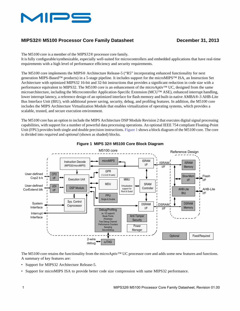
MIPS32® M5100 Processor Core Family Datasheet December 31, 2013 1 MIPS32® M5100 Processor Core Family Datasheet, Revision 01.00 The M5100 core is a member of the MIPS32® processor core family. It is fully configurable/synthesizable, especially well-suited for microcontrollers and embedded applications that have real-time requirements with a high level of performance efficiency and security requirements. The M5100 core implements the MIPS® Architecture Release-5 (“R5” incorporating enhanced functionality for next generation MIPS-Based™ products) in a 5-stage pipeline. It includes support for the microMIPS™ ISA, an Instruction Set Architecture with optimized MIPS32 16-bit and 32-bit instructions that provides a significant reduction in code size with a performance equivalent to MIPS32. The M5100 core is an enhancement of the microAptiv™ UC, designed from the same microarchitecture, including the Microcontroller Application-Specific Extension (MCU™ ASE), enhanced interrupt handling, lower interrupt latency, a reference design of an optimized interface for flash memory and built-in native AMBA®-3 AHB-Lite Bus Interface Unit (BIU), with additional power saving, security, debug, and profiling features. In addition, the M5100 core includes the MIPS Architecture Virtualization Module that enables virtualization of operating systems, which provides a scalable, trusted, and secure execution environment. The M5100 core has an option to include the MIPS Architecture DSP Module Revision 2 that executes digital signal processing capabilities, with support for a number of powerful data processing operations. An optional IEEE 754 compliant Floating-Point Unit (FPU) provides both single and double precision instructions. Figure 1 shows a block diagram of the M5100 core. The core is divided into required and optional (shown as shaded) blocks. Figure 1 MIPS 32® M5100 Core Block Diagram The M5100 core retains the functionality from the microAptiv™ UC processor core and adds some new features and functions. A summary of key features are: • Support for MIPS32 Architecture Release-5. • Support for microMIPS ISA to provide better code size compression with same MIPS32 performance. Fixed/Required Optional Flash I/F AHB-Lite I/F ISRAM I/F DSRAM I/F Instruction Decode (MIPS32/microMIPS) User-defined Cop2 b k User-defined CorExtend blk CP2 I/F UDI I/F GPR (1,2,4,8,16 sets) microMIPS ISRAM I/F SRAM Controller DSRAM I/F System Interface Interrupt Interface M5100 core ISRAM Memory Slow Mem I/F AHB-Lite BIU Reference Design cJTAG 2-wire debug Sys. Control Coprocessor Debug/Profiling (w. VZ support) Break Points iFlowtrace Fast Debug Channel Performance Counters Sampling SecureDebug DSRAM Memory Power Manager Anti-Tamper Security MMU Virtualization support for Root & Guest Execution Unit MDU FPU Single & Double DSP Module
Transcript of MIPS32® M5100 Processor Core Family Datasheet December 31 ...€¦ · 4 MIPS32® M5100 Processor...
MIPS32® M5100 Processor Core Family Datasheet December 31, 2013
1 MIPS32® M5100 Processor Core Family Datasheet, Revision 01.00
The M5100 core is a member of the MIPS32® processor core family.It is fully configurable/synthesizable, especially well-suited for microcontrollers and embedded applications that have real-timerequirements with a high level of performance efficiency and security requirements.
The M5100 core implements the MIPS® Architecture Release-5 (“R5” incorporating enhanced functionality for nextgeneration MIPS-Based™ products) in a 5-stage pipeline. It includes support for the microMIPS™ ISA, an Instruction SetArchitecture with optimized MIPS32 16-bit and 32-bit instructions that provides a significant reduction in code size with aperformance equivalent to MIPS32. The M5100 core is an enhancement of the microAptiv™ UC, designed from the samemicroarchitecture, including the Microcontroller Application-Specific Extension (MCU™ ASE), enhanced interrupt handling,lower interrupt latency, a reference design of an optimized interface for flash memory and built-in native AMBA®-3 AHB-LiteBus Interface Unit (BIU), with additional power saving, security, debug, and profiling features. In addition, the M5100 coreincludes the MIPS Architecture Virtualization Module that enables virtualization of operating systems, which provides ascalable, trusted, and secure execution environment.
The M5100 core has an option to include the MIPS Architecture DSP Module Revision 2 that executes digital signal processingcapabilities, with support for a number of powerful data processing operations. An optional IEEE 754 compliant Floating-PointUnit (FPU) provides both single and double precision instructions. Figure 1 shows a block diagram of the M5100 core. The coreis divided into required and optional (shown as shaded) blocks.
Figure 1 MIPS 32® M5100 Core Block Diagram
The M5100 core retains the functionality from the microAptiv™ UC processor core and adds some new features and functions.A summary of key features are:
• Support for MIPS32 Architecture Release-5.
• Support for microMIPS ISA to provide better code size compression with same MIPS32 performance.
Fixed/RequiredOptional
FlashI/F
AHB-LiteI/F
ISRAMI/F
DSRAMI/F
Instruction Decode(MIPS32/microMIPS)
User-definedCop2 b k
User-definedCorExtend blk
CP2I/F
UDII/F
GPR(1,2,4,8,16 sets)
microMIPS ISRAMI/F
SRAMController
DSRAMI/F
SystemInterface
InterruptInterface
M5100 core
ISRAMMemory
Slow MemI/F
AHB-LiteBIU
Reference Design
cJTAG2-wiredebug
Sys. ControlCoprocessor
Debug/Profiling(w. VZ support)
Break PointsiFlowtrace
Fast Debug ChannelPerformance Counters
SamplingSecureDebug
DSRAMMemory
PowerManager
Anti-TamperSecurity
MMU
Virtualizationsupport for
Root & Guest
Execution Unit
MDU
FPUSingle & Double
DSP Module

2 MIPS32® M5100 Processor Core Family Datasheet, Revision 01.00
• Support for multiple shadow register sets.
• The Memory Management Unit (MMU), consisting of asimple, Fixed Mapping Translation (FMT) mechanism.
• Supports configurable DSP Module Revision 2 for digitalsignal processing capabilities.
• Multiply/Divide Unit (MDU) - If the DSP is notincluded, the MDU can be configured for eitherperformance or area optimizations. The high-performance optimization supports a single-cycle 32x16-bit MAC instruction or two-cycle 32x32-bit instructions.If the DSP is included, the MDU is enhanced with ahardware multiplier array supporting single-cycle 32x32MAC and DSP instructions.
• Floating-Point Unit (FPU), an IEEE-754 compliantFloating-Point Unit with single and double precisiondatatypes.
• A simple SRAM-style interface that is configurable forindependent instruction and data or as a unified interface.The SRAM interface enables deterministic response,while maintaining high-performance operation
• Support for the MCU ASE to enhance common functionsused in microcontroller applications such as interruptsand semaphore manipulation.
• Security features such as the SecureDebug to restrictuntrusted EJTAG debug access.
• Support for the Virtualization Module via privileged(root) and unprivileged (guest) operating modes. Legacysoftware will run in guest mode where all operations aremonitored and trapped by hypervisor software if theguest does not behave as expected. The hypervisoroperates invisibly to the guest, and enforces dataprotection between guests.
• Reference design for SRAM interface to AMBA-3 AHB-Lite bus and flash memory.
• Parity support.
• An optional Enhanced JTAG (EJTAG version 4.52)block allows for single-stepping of the processor as wellas instruction and data virtual address/value breakpoints.iFlowtrace™ version 2.0 is also supported to add real-time instruction program counter and special events tracecapability for debug. Additionally, Fast Debug Channel,Performance Counters, and PC/Data sampling functionsare added to enrich debug and profiling features on theM5100 core.
• External block to convert 4-wire EJTAG (IEEE 1149.1)interface to 2-wire cJTAG (IEEE 1149.7) interface.
• Configurable hardware breakpoints triggered by addressmatch or address range.
Features• 5-stage pipeline
• 32-bit Address and Data Paths
• MIPS32 Instruction Set Architecture
• MIPS32 Enhanced Architecture Features
• Vectored interrupts and support for external inter-rupt controller
• Programmable exception vector base
• Atomic interrupt enable/disable
• GPR shadow registers (one, three, seven, or fifteenadditional shadows can be optionally added to min-imize latency for interrupt handlers)
• Bit field manipulation instructions
• microMIPS Instruction Set Architecture
• microMIPS ISA is a build-time configurable optionthat reduces code size over MIPS32, while main-taining MIPS32 performance.
• Combining both 16-bit and 32-bit opcodes, micro-MIPS supports all MIPS32 instructions (exceptbranch-likely instructions) with new optimizedencoding. Frequently used MIPS32 instructions areavailable as 16-bit instructions.
• Added fifteen new 32-bit instructions and thirty-nine 16-bit instructions.
• Stack pointer implicit in instruction.
• MIPS32 assembly and ABI-compatible.
• Supports MIPS architecture Modules and User-defined Instructions (UDIs).
• MCU™ ASE
• Increases the number of interrupt hardware inputsfrom 6 to 8 for Vectored Interrupt (VI) mode, andfrom 63 to 255 for External Interrupt Controller(EIC) mode.
• Separate priority and vector generation. 16-bit vec-tor address is provided.
• Hardware assist combined with the use of ShadowRegister Sets to reduce interrupt latency during theprologue and epilogue of an interrupt.
• An interrupt return with automated interrupt epi-logue handling instruction (IRET) improves inter-rupt latency.
• Supports optional interrupt chaining.
• Two memory-to-memory atomic read-modify-writeinstructions (ASET and ACLR) eases commonlyused semaphore manipulation in microcontrollerapplications. Interrupts are automatically disabledduring the operation to maintain coherency.

MIPS32® M5100 Processor Core Family Datasheet, Revision 01.00 3
• Memory Management Unit
• Simple Fixed Mapping Translation (FMT) mecha-nism
• Virtualization Module Support
• Support for the Virtualization Module using “trapand emulate” techniques.
• Two new operating modes: privileged (root) andunprivileged (guest)
• System resources controlled through privilegedinstructions while executing in privileged mode
• Execution of a privileged instruction in unprivi-leged mode will cause an exception (trap), returningcontrol to privileged-mode software
• Address translation is performed on the entireaddress space when in unprivileged mode
• Configurable from 1 to 7 guests
• Supports RPU (Root Protection Unit) memorymanagement unit
• Simple SRAM-Style Interface
• 32-bit address and data; input byte-enables enablesimple connection to narrower devices
• Single or multi-cycle latencies
• Configuration option for dual or unified instruction/data interfaces
• Redirection mechanism on dual I/D interfaces per-mits D-side references to be handled by I-side
• Transactions can be aborted
• Reference Design
• A typical SRAM reference design is provided.
• An AHB-Lite BIU reference design is providedbetween the SRAM interface and AHB-Lite Bus.
• An optimized interface for slow memory (Flash)access using prefetch buffer scheme is provided.
• Parity Support
• The ISRAM and DSRAM support optional paritydetection.
• MIPS DSP Module (Revision 2.0)
• Support for MAC operations with 3 additional pairsof Hi/Lo accumulator registers (Ac0 - Ac3)
• Fractional data types (Q15, Q31) with roundingsupport
• Saturating arithmetic with overflow handling
• SIMD instructions operate on 2x16-bit or 4x8-bitoperands simultaneously
• Separate MDU pipeline with full-sized hardwaremultiplier to support back-to-back operations
• The DSP Module is build-time configurable.
• Multiply/Divide Unit (high-performance configurationwithout DSP)
• Maximum issue rate of one 32x16 multiply perclock via on-chip 32x16 hardware multiplier array.
• Maximum issue rate of one 32x32 multiply everyother clock
• Early-in iterative divide. Minimum 11 and maxi-mum 34 clock latency (dividend (rs) sign exten-sion-dependent)
• Multiply/Divide Unit (with DSP configuration)
• Maximum issue rate of one 32x32 multiply perclock via on-chip 32x32 hardware multiplier array
• Maximum issue rate of one 32x32 multiply everyclock
• Early-in iterative divide. Minimum 12 and maxi-mum 38clock latency (dividend (rs) sign extension-dependent)
• Multiply/Divide Unit (area-efficient configurationwithout DSP)
• 32 clock latency on multiply
• 34 clock latency on multiply-accumulate
• 33-35 clock latency on divide (sign-dependent)
• Floating Point Unit (FPU)
• 1985 IEEE-754 compliant Floating Point Unit.
• Supports single and double precision datatypes
• 2008 IEEE-754 compatibility control for NaN han-dling and Abs/Neg instructions
• Runs at 1:1 core/FPU clock ratio.
• The FPU is build-time configurable.
• CorExtend® User-Defined Instruction Set Extensions
• Allows user to define and add instructions to thecore at build time
• Maintains full MIPS32 compatibility
• Supported by industry-standard development tools
• Single or multi-cycle instructions
• Multi-Core Support
• External lock indication enables multi-processorsemaphores based on LL/SC instructions
• External sync indication allows memory ordering
• Debug support includes cross-core triggers
• Coprocessor 2 interface
• 32-bit interface to an external coprocessor
• Anti-Tamper Security Features

4 MIPS32® M5100 Processor Core Family Datasheet, Revision 01.00
• Injection of random pipeline slips controlled viaCP0 register
• Fast general-purpose 32-bit pseudo random genera-tor accessible via CP0 register
• Complex pseudo random generator for hardwareuse controlled via user-defined seed
• Power Control
• Minimum frequency: 0 MHz
• Power-down mode (triggered by WAIT instruction)
• Support for software-controlled clock divider
• Support for extensive use of local gated clocks
• EJTAG Debug/Profiling and iFlowtrace™ Mechanism
• CPU control with start, stop, and single stepping
• Virtual instruction and data address/value break-points
• Hardware breakpoint supports both address matchand address range triggering
• Optional simple hardware breakpoints on virtualaddresses; 8I/4D, 6I/2D, 4I/2D, 2I/1D breakpoints,or no breakpoints
• Optional complex hardware breakpoints with 8I/4D, 6I/2D simple breakpoints
• TAP controller is chainable for multi-CPU debug
• Supports EJTAG (IEEE 1149.1) and compatiblewith cJTAG 2-wire (IEEE 1149.7) extension proto-col
• Cross-CPU breakpoint support
• iFlowtrace support for real-time instruction PC andspecial events
• PC and/or load/store address sampling for profiling
• Performance Counters
• Support for Fast Debug Channel (FDC)
• SecureDebug
• An optional feature that disables access via EJTAGin an untrusted environment
• Testability
• Full scan design achieves test coverage in excess of99% (dependent on library and configurationoptions)
Architecture Overview
The M5100 core contains both required and optional blocks,as shown in Figure 1. Required blocks must be implementedto remain MIPS-compliant. Optional blocks can be added tothe M5100 core based on the needs of the implementation.
The required blocks are as follows:
• Instruction Decode
• Execution Unit
• General Purposed Registers (GPR)
• Multiply/Divide Unit (MDU)
• System Control Coprocessor (CP0)
• Memory Management Unit (MMU)
• I/D SRAM Interfaces
• Power Management
Optional or configurable blocks include:
• Configurable instruction decoder supporting three ISAmodes: MIPS32-only, MIPS32 and microMIPS, ormicroMIPS-only
• DSP (integrated with MDU)
• Floating-point Unit (FPU)
• Virtualization support (integrated with MMU)
• Reference Design of I/D-SRAM, BIU, Slow MemoryInterface
• Anti-Tamper Security Block
• Coprocessor 2 interface
• CorExtend® User-Defined Instruction (UDI) interface
• Debug/Profiling with Enhanced JTAG (EJTAG)Controller, Break points, Sampling, Performancecounters, Fast Debug Channel, and iFlowtrace logic
The section "MIPS32® M5100 Core Required Logic Blocks"on page 6 discusses the required blocks. The section"MIPS32® M5100 Core Optional or Configurable LogicBlocks" on page 12 discusses the optional blocks.
Pipeline Flow
The M5100 core implements a 5-stage pipeline with aperformance similar to the microAptiv™ UC pipeline. Thepipeline allows the processor to achieve high frequency whileminimizing device complexity, reducing both cost and powerconsumption.
The M5100 core pipeline consists of five stages:
• Instruction (I Stage)
• Execution (E Stage)
• Memory (M Stage)
• Align (A Stage)
• Writeback (W stage)

MIPS32® M5100 Processor Core Family Datasheet, Revision 01.00 5
The M5100 core implements a bypass mechanism that allowsthe result of an operation to be forwarded directly to theinstruction that needs it without having to write the result tothe register and then read it back.
Figure 2 shows a timing diagram of the M5100 core pipeline(shown with the-high performance MDU ).
Figure 2 MIPS32® M5100 Core Pipeline
I Stage: Instruction Fetch
During the Instruction fetch stage:
• An instruction is fetched from the instructionSRAM.
• If both MIPS32 and microMIPS ISAs are supported,microMIPS instructions are converted to MIPS32-likeinstructions. If the MIPS32 ISA is not supported, 16-bitmicroMIPS instructions will be first recoded into 32-bitmicroMIPS equivalent instructions, and then decoded innative microMIPS ISA format.
E Stage: Execution
During the Execution stage:
• Operands are fetched from the register file.
• Operands from the M and A stage are bypassed to thisstage.
• The Arithmetic Logic Unit (ALU) begins the arithmeticor logical operation for register-to-register instructions.
• The ALU calculates the virtual data address for load andstore instructions, and the MMU performs the fixedvirtual-to-physical address translation.
• The ALU determines whether the branch condition istrue and calculates the virtual branch target address forbranch instructions.
• Instruction logic selects an instruction address and theMMU performs the fixed virtual-to-physical addresstranslation.
• All multiply and divide operations begin in this stage.
M Stage: Memory Fetch
During the Memory fetch stage:
• The arithmetic ALU operation completes.
• The data SRAM access is performed for load and storeinstructions.
• A 32x32 multiply calculation completes (with DSPconfiguration).
• A 32x32 multiply operation stalls the MDU pipeline forone clock in the M stage (high-performance MDU optionwithout DSP configuration).
• A multiply operation stalls the MDU pipeline for 31clocks in the M stage (area-efficient MDU option withoutDSP configuration).
• A multiply-accumulate operation stalls the MDU pipelinefor 33 clocks in the M stage (area-efficient MDU optionwithout DSP configuration).
• A divide operation stalls the MDU pipeline for amaximum of 38 clocks in the M stage. Early-in signextension detection on the dividend will skip 7, 15, or 23stall clocks (only the divider in the fast MDU optionsupports early-in detection).
A Stage: Align
During the Align stage:
• Load data is aligned to its word boundary.
• A multiply/divide operation updates the HI/LO registers(area-efficient MDU option).
• Multiply operation performs the carry-propagate-add.The actual register writeback is performed in the W stage(high-performance MDU option).
• A MUL operation makes the result available forwriteback. The actual register writeback is performed inthe W stage.
• EJTAG complex break conditions are evaluated.
W Stage: Writeback
During the Writeback stage:
• For register-to-register or load instructions, theinstruction result is written back to the register file.
Virtualization Module
The Virtualization Module is supported in the M5100 core.Virtualization defines a set of extensions to the MIPS32
I E M A W
I-A1
RegRdI Dec
ALU OpAlign RegWD-AC
BypassBypass
Mult RegW
Bypass
Acc
I-A2
Div RegWAcc
I-SRAMD-SRAM
6 MIPS32® M5100 Processor Core Family Datasheet, Revision 01.00
Architecture for efficient implementation of virtualizedsystems.
Virtualization is enabled by software—the key element is acontrol program known as a Virtual Machine Monitor(VMM) or hypervisor. The hypervisor is in full control ofmachine resources at all times.
When an operating system (OS) kernel runs within a virtualmachine (VM), it becomes a guest of the hypervisor. Alloperations performed by a guest must be explicitly permittedby the hypervisor. To ensure that it remains in control, thehypervisor always runs at a higher level of privilege than aguest operating system kernel.
The hypervisor is responsible for managing access tosensitive resources, maintaining the expected behavior foreach VM, and sharing resources between multiple VMs.
In a traditional operating system, the kernel (or supervisor)typically runs at a higher level of privilege than userapplications. The kernel provides a protected virtual-memoryenvironment for each user application, inter-processcommunications, IO device sharing and transparent contextswitching. The hypervisor performs the same basic functionsin a virtualized system, except that the hypervisor’s clientsare full operating systems rather than user applications.
The virtual machine execution environment created andmanaged by the hypervisor consists of the full Instruction SetArchitecture, including all Privileged Resource Architecturefacilities, plus any device-specific or board-specificperipherals and associated registers. It appears to each guestoperating system as if it is running on a real machine with fulland exclusive control.
The Virtualization Module enables full virtualization, and isintended to allow VM scheduling to take place while meetingreal-time requirements, and to minimize costs of contextswitching between VMs.
MIPS32® M5100 Core RequiredLogic Blocks
The required logic blocks of the M5100 core (Figure 1) aredefined in the following subsections.
Execution Unit
The M5100 core execution unit implements a load/storearchitecture with single-cycle ALU operations (logical, shift,add, subtract) and an autonomous multiply/divide unit.
The execution unit includes:
• Arithmetic Logic Unit (ALU) for performing arithmeticand bitwise logical operations. Shared adder forarithmetic operations, load/store address calculation, andbranch target calculation.
• Address unit for calculating the next PC and next fetchaddress selection muxes.
• Load Aligner.
• Shifter and Store Aligner.
• Branch condition comparator.
• Trap condition comparator.
• Bypass muxes to advance result between two adjacentinstructions with data dependency.
• Leading Zero/One detect unit for implementing the CLZand CLO instructions.
• Actual execution of the Atomic Instructions defined inthe MCU ASE.
• A separate DSP ALU and Logic block for performingpart of DSP Module instructions, such as arithmetic/shift/compare operations if the DSP function is configured.
General Purpose Registers
The M5100 core contains thirty-two 32-bit general-purposeregisters used for integer operations and address calculation.Optionally, one, three, seven or fifteen additional register fileshadow sets (each containing thirty-two registers) can beadded to minimize context switching overhead duringinterrupt/exception processing. The register file consists oftwo read ports and one write port and is fully bypassed tominimize operation latency in the pipeline.
Multiply/Divide Unit (MDU)
The M5100 core includes a multiply/divide unit (MDU) thatcontains a separate, dedicated pipeline for integer multiply/divide operations, and DSP Module multiply instructions.This pipeline operates in parallel with the integer unit (IU)pipeline and does not stall when the IU pipeline stalls. Thisallows the long-running MDU operations to be partiallymasked by system stalls and/or other integer unit instructions.
The MIPS architecture defines that the result of a multiply ordivide operation be placed in a pair (without DSP enabled) orone of 4 pairs (with DSP enabled) of HI and LO registers.Using the Move-From-HI (MFHI) and Move-From-LO(MFLO) instructions, these values can be transferred to thegeneral-purpose register file.
There are three configuration options for the MDU: 1) a full32x32 multiplier block; 2) a higher performance 32x16multiplier block; 3) an area-efficient iterative multiplier

MIPS32® M5100 Processor Core Family Datasheet, Revision 01.00 7
block. Option 2 and 3 are available if the DSP configurationoption is disabled. If the DSP configuration option is enabled,option 1 is the default. The selection of the MDU style allowsthe implementor to determine the appropriate performanceand area trade-off for the application.
MDU with 32x32 DSP Multiplier
With the DSP configuration option enabled, the MDUsupports execution of one 16x16, 32x16, or 32x32 multiply ormultiply-accumulate operation every clock cycle with thebuilt in 32x32 multiplier array. The multiplier is shared withDSP Module operations.
The MDU also implements various shift instructionsoperating on the HI/LO register and multiply instructions asdefined in the DSP Module. It supports all the data typesrequired for this purpose and includes three extra HI/LOregisters as defined by the Module.
Table 1 lists the latencies (throughput with data dependency)and repeat rates (throughput without data dependency) for theDSP multiply and dot-product operations. The approximatelatencies and repeat rates are listed in terms of pipelineclocks. For a more detailed discussion of latencies and repeatrates, refer to the MIPS32 M5100 Processor Core SoftwareUser’s Manual.
MDU with 32x16 High-Performance Multiplier
The high-performance MDU consists of a 32x16 Booth-recoded multiplier, a pair of result/accumulation registers (HIand LO), a divide state machine, and the necessarymultiplexers and control logic. The first number shown (‘32’of 32x16) represents the rs operand. The second number (‘16’of 32x16) represents the rt operand. The M5100 core onlychecks the value of the rt operand to determine how manytimes the operation must pass through the multiplier. The
16x16 and 32x16 operations pass through the multiplier once.A 32x32 operation passes through the multiplier twice.
The MDU supports execution of one 16x16 or 32x16multiply or multiply-accumulate operation every clock cycle;32x32 multiply operations can be issued every other clockcycle. Appropriate interlocks are implemented to stall theissuance of back-to-back 32x32 multiply operations. Themultiply operand size is automatically determined by logicbuilt into the MDU.
Table 2, Table 3 and Table 4 list the repeat rate (how often theoperation can be reissued when there is no data dependency)and latency (number of cycles until a result is available) forthe multiply and divide instructions. The approximate latencyand repeat rates are listed in terms of pipeline clocks. For amore detailed discussion of latencies and repeat rates, refer toChapter 2 of the MIPS32 M5100 Processor Core FamilySoftware User’s Manual.
Table 1 DSP-related Latencies and Repeat Rates
Opcode LatencyRepeat
Rate
Multiply and dot-product without satu-ration after accumula-tion
5 1
Multiply and dot-product with satura-tion after accumula-tion
5 1
Multiply withoutaccumulation
5 1
Table 2 High-Performance Integer Multiply/DivideUnit Latencies and Repeat Rates with DSP
Opcode
OperandSize
(mul rt)(div rs) Latency
RepeatRate
MUL(GPR destination)
16 bits 5 1
32 bits 5 1
MULT, MULTU,MADD, MADDU,MSUB, MSUBU(Hi/Lo destination)
16 bits 5 1
32 bits 5 1
DIV / DIVU(Hi/Lo destination)
8 bits 12-14 / 12 12-14 / 12
16 bits 20-22 / 20 20-22 / 20
24 bits 28-30 / 30 28-30 / 30
32 bits 35-37 / 35 35-37 / 35
Table 3 High-Performance Integer Multiply/DivideUnit Latencies and Repeat Rates without DSP
Opcode
OperandSize
(mul rt)(div rs) Latency
RepeatRate
MUL(GPR destination)
16 bits 5 2
32 bits 6 3

8 MIPS32® M5100 Processor Core Family Datasheet, Revision 01.00
MDU with Area-Efficient Option
With the area-efficient option, multiply and divide operationsare implemented with a simple 1-bit-per-clock iterativealgorithm. Any attempt to issue a subsequent MDUinstruction while a multiply/divide is still active causes anMDU pipeline stall until the operation is completed.
Table 4 lists the latency (number of cycles until a result isavailable) for the M5100 core multiply and divideinstructions. The latencies are listed in terms of pipelineclocks.
Regardless of the multiplier array implementation, divideoperations are implemented with a simple 1-bit-per-clock
iterative algorithm. An early-in detection checks the signextension of the dividend (rs) operand. If rs is 8 bits wide, 23iterations are skipped. For a 16-bit-wide rs, 15 iterations areskipped, and for a 24-bit-wide rs, 7 iterations are skipped.Any attempt to issue a subsequent MDU instruction while adivide is still active causes an IU pipeline stall until the divideoperation has completed.
System Control Coprocessor (CP0)
In the MIPS architecture, CP0 is responsible for the virtual-to-physical address translation, the exception control system,the processor’s diagnostics capability, the operating modes(kernel, user, and debug), and whether interrupts are enabledor disabled. Configuration information, such as presence ofbuild-time options like microMIPS, CorExtend Module orCoprocessor 2 interface, is also available by accessing theCP0 registers.
Coprocessor 0 also contains the logic for identifying andmanaging exceptions. Exceptions can be caused by a varietyof sources, including boundary cases in data, external events,or program errors.
Interrupt Handling
The M5100 core includes support for eight hardwareinterrupt pins, two software interrupts, and a timer interrupt.These interrupts can be used in any of three interrupt modes,as defined by Release 2 of the MIPS32 Architecture:
• Interrupt compatibility mode, which acts identically tothat in an implementation of Release 1 of theArchitecture.
• Vectored Interrupt (VI) mode, which adds the ability toprioritize and vector interrupts to a handler dedicated tothat interrupt, and to assign a GPR shadow set for useduring interrupt processing. The presence of this mode isdenoted by the VInt bit in the Config3 register. Thismode is architecturally optional; but it is always presenton the M5100 core, so the VInt bit will always read as a1 for the M5100 core.
• External Interrupt Controller (EIC) mode, whichredefines the way in which interrupts are handled toprovide full support for an external interrupt controllerhandling prioritization and vectoring of interrupts. Thepresence of this mode denoted by the VEIC bit in theConfig3 register. Again, this mode is architecturallyoptional. On the M5100 core, the VEIC bit is setexternally by the static input, SI_EICPresent, to allowsystem logic to indicate the presence of an externalinterrupt controller.
MULT, MULTU,MADD, MADDU,MSUB, MSUBU(Hi/Lo destination)
16 bits 2 1
32 bits 3 2
DIV / DIVU(Hi/Lo destination)
8 bits 11-12 / 11 11-12 / 11
16 bits 19-20 / 19 19-20 / 19
24 bits 27-28 / 27 27-28 / 27
32 bits 34-35 / 34 34-35 / 34
Table 4 Area-Efficient Integer Multiply/Divide UnitOperation Latencies without DSP
Opcode
OperandSize
(mul rt)(div rs) Latency
RepeatRate
MUL(GPR destination)
any 35 32
MULT, MULTU,(Hi/Lo destination)
any 32 32
MADD, MADDU,MSUB, MSUBU(Hi/Lo destination)
any 34 34
DIV / DIVU(Hi/Lo destination)
any 33-34 / 33 33-34 / 33
Table 3 High-Performance Integer Multiply/DivideUnit Latencies and Repeat Rates without DSP
Opcode
OperandSize
(mul rt)(div rs) Latency
RepeatRate

MIPS32® M5100 Processor Core Family Datasheet, Revision 01.00 9
The reset state of the processor is interrupt compatibilitymode, such that a processor supporting Release 2 of theArchitecture, the M5100 core for example, is fullycompatible with implementations of Release 1 of theArchitecture.
VI or EIC interrupt modes can be combined with the optionalshadow registers to specify which shadow set should be usedon entry to a particular vector. The shadow registers furtherimprove interrupt latency by avoiding the need to savecontext when invoking an interrupt handler.
In the M5100 core, interrupt latency is reduced by:
• Speculative interrupt vector prefetching during thepipeline flush.
• Interrupt Automated Prologue (IAP) in hardware:Shadow Register Sets remove the need to save GPRs,and IAP removes the need to save specific ControlRegisters when handling an interrupt.
• Interrupt Automated Epilogue (IAE) in hardware:Shadow Register Sets remove the need to restore GPRs,and IAE removes the need to restore specific ControlRegisters when returning from an interrupt.
• Allow interrupt chaining. When servicing an interruptand interrupt chaining is enabled, there is no need toreturn from the current Interrupt Service Routine (ISR) ifthere is another valid interrupt pending to be serviced.The control of the processor can jump directly from thecurrent ISR to the next ISR without IAE and IAP.
GPR Shadow Registers
The MIPS32 Architecture optionally removes the need tosave and restore GPRs on entry to high-priority interrupts orexceptions, and to provide specified processor modes withthe same capability. This is done by introducing multiplecopies of the GPRs, called shadow sets, and allowingprivileged software to associate a shadow set with entry tokernel mode via an interrupt vector or exception. The normalGPRs are logically considered shadow set zero.
The number of GPR shadow sets is a build-time option. TheM5100 core allows 1 (the normal GPRs), 2, 4, 8, or 16shadow sets. The highest number actually implemented isindicated by the SRSCtlHSS field. If this field is zero, only thenormal GPRs are implemented.
Shadow sets are new copies of the GPRs that can besubstituted for the normal GPRs on entry to kernel mode viaan interrupt or exception. Once a shadow set is bound to akernel-mode entry condition, references to GPRs operateexactly as one would expect, but they are redirected toregisters that are dedicated to that condition. Privilegedsoftware may need to reference all GPRs in the register file,even specific shadow registers that are not visible in thecurrent mode, and the RDPGPR and WRPGPR instructionsare used for this purpose. The CSS field of the SRSCtl registerprovides the number of the current shadow register set, andthe PSS field of the SRSCtl register provides the number of theprevious shadow register set that was current before the lastexception or interrupt occurred.
If the processor is operating in VI interrupt mode, binding ofa vectored interrupt to a shadow set is done by writing to theSRSMap register. If the processor is operating in EIC interruptmode, the binding of the interrupt to a specific shadow set isprovided by the external interrupt controller and is configuredin an implementation-dependent way. Binding of anexception or non-vectored interrupt to a shadow set is doneby writing to the ESS field of the SRSCtl register. When anexception or interrupt occurs, the value of SRSCtlCSS is copiedto SRSCtlPSS, and SRSCtlCSS is set to the value taken from theappropriate source. On an ERET, the value of SRSCtlPSS iscopied back into SRSCtlCSS to restore the shadow set of themode to which control returns.
Modes of Operation
The M5100 core implements the Virtualization Module bysupporting five modes of operation:
• Guest-user mode is most often used for applicationsprograms.
• Guest-kernel mode is typically used for handlingexceptions and operating-system kernel functions,including CP0 management and I/O deviceaccesses.
• Root-user mode is used to run hypervisor (VirtualMachine Monitor (VMM)) user software.
• Root-kernel mode is used to run hypervisor (VirtualMachine Monitor (VMM)) kernel software.
• Debug mode is used during system bring-up andsoftware development. Refer to the EJTAG sectionfor more information on debug mode.
Figure 3 shows the virtual address map of the MIPSArchitecture.

10 MIPS32® M5100 Processor Core Family Datasheet, Revision 01.00
Figure 3 M5100 Core Virtual Address Map
Memory Management Unit (MMU) in GuestModes
The M5100 core contains a simple Fixed MappingTranslation (FMT) MMU that interfaces between theexecution unit and the SRAM controller.
Fixed Mapping Translation (FMT)
A FMT is smaller and simpler than the full TranslationLookaside Buffer (TLB) style MMU found in other MIPScores. Like a TLB, the FMT performs virtual-to-physicaladdress translation and provides attributes for the differentsegments. Those segments that are unmapped in a TLBimplementation (kseg0 and kseg1) are translated identicallyby the FMT.
Memory Management Unit (MMU) in RootModes
The M5100 core provides a Root Protection Unit (RPU)MMU for guest virtual-address protection.
Root Protection Unit (RPU)
A RPU-based MMU is similar to an RTLB in that it consistsof 8, 16, or 32 dual-entry fully associative look-aside buffer,but the segments that are unmapped in a TLB implementation(kseg0 and kseg1) are translated identically by the RPU.
The RPU allows guest pages to be protected by a read-inhibit,execute-inhibit, and write-protection attribute.
When an instruction address is calculated, the virtual addressis first compared to the contents of the 4-entry IFMT . If theaddress is not found, the virtual address is fixed mapped andvalidated by the RPU. If the address is not found in the RPU,a refill exception is taken.
When a data address is calculated, the virtual address iscompared to the 4-entry DFMT . If the address is not found,the virtual address is fixed mapped and validated by the RPU.If the address is not found in the RPU, a refill exception istaken.
Figure 4 shows how the FMT is implemented in the M5100core.
Figure 4 Address Translation During SRAM Accesswith FMT Implementation
SRAM Interface Controller
Instead of caches, the M5100 core contains an interface toSRAM-style memories that can be tightly coupled to the core.This permits deterministic response time with less area thanis typically required for caches. The SRAM interface includesseparate uni-directional 32-bit buses for address, read data,and write data.
Dual or Unified Interfaces
The SRAM interface includes a build-time option to selecteither dual or unified instruction and data interfaces.
The dual interface enables independent connection toinstruction and data devices. It generally yields the highest
kuseg
kseg0
kseg1
kseg2
kseg3
0x00000000
0x7FFFFFFF0x80000000
0x9FFFFFFF0xA0000000
0xBFFFFFFF0xC0000000
0xDFFFFFFF0xE0000000
0xF1FFFFFF
Kernel Virtual Address Space
Unmapped, 512 MBKernel Virtual Address Space
Uncached
Unmapped, 512 MBKernel Virtual Address Space
User Virtual Address Space
1. This space is mapped to memory in user or kernel mode,and by the EJTAG module in debug mode.
0xFF2000000xFF3FFFFF0xFF400000
0xFFFFFFFF
Memory/EJTAG1
Mapped, 2048 MB
Fixed Mapped, 512 MB
Fixed Mapped
Fixed Mapped
guest IVAEntry
IFMT
FMT MMU
DFMT
Entry
guest DVA
guest IVARoot IPA
Root DPA
RPUSRAM
Interface
DataSRAM
InstSRAM

MIPS32® M5100 Processor Core Family Datasheet, Revision 01.00 11
performance, because the pipeline can generate simultaneousI and D requests, which are then serviced in parallel.
For simpler or cost-sensitive systems, it is also possible tocombine the I and D interfaces into a common interface thatservices both types of requests. If I and D requests occursimultaneously, priority is given to the D side.
Back-stalling
Typically, read and write transactions will complete in asingle cycle. However, if multi-cycle latency is desired, theinterface can be stalled to allow connection to slower devices.
Redirection
When the dual I/D interface is present, a mechanism exists todivert D-side references to the I-side, if desired. Themechanism can be explicitly invoked for any other D-sidereferences, as well. When the DS_Redir signal is asserted, aD-side request is diverted to the I-side interface in thefollowing cycle, and the D-side will be stalled until thetransaction is completed.
Transaction Abort
The core may request a transaction (fetch/load/store/sync) tobe aborted. This is particularly useful in case of interrupts.Because the core does not know whether transactions are re-startable, it cannot arbitrarily interrupt a request which hasbeen initiated on the SRAM interface. However, cycles spentwaiting for a multi-cycle transaction to complete can directlyimpact interrupt latency. In order to minimize this effect, theinterface supports an abort mechanism. The core requests anabort whenever an interrupt is detected and a transaction ispending (abort of an instruction fetch may also be requestedin other cases). The external system logic can choose toacknowledge or to ignore the abort request.
Connecting to Narrower Devices
The instruction and data read buses are always 32 bits inwidth. To facilitate connection to narrower memories, theSRAM interface protocol includes input byte-enables that canbe used by system logic to signal validity as partial read databecomes available. The input byte-enables conditionallyregister the incoming read data bytes within the core, and thuseliminate the need for external registers to gather the entire 32bits of data. External muxes are required to redirect thenarrower data to the appropriate byte lanes.
Lock Mechanism
The SRAM interface includes a protocol to identify a lockedsequence, and is used in conjunction with the LL/SC atomicread-modify-write semaphore instructions.
Sync Mechanism
The interface includes a protocol that externalizes theexecution of the SYNC instruction. External logic mightchoose to use this information to enforce memory orderingbetween various elements in the system.
External Call Indication
The instruction fetch interface contains signals that indicatethat the core is fetching the target of a subroutine call-typeinstruction such as JAL or BAL. At some point after a call,there will typically be a return to the original code sequence.If a system prefetches instructions, it can make use of thisinformation to save instructions that were prefetched and arelikely to be executed after the return.
Hardware Reset
The M5100 core has two types of reset input signals:SI_Reset and SI_ColdReset. Functionally, these two signalsare ORed together within the core and then used to initializecritical hardware state.
Both reset signals can be asserted either synchronously orasynchronously to the core clock, SI_ClkIn, and will trigger aReset exception. The reset signals are active high and must beasserted for a minimum of 5 SI_ClkIn cycles. The falling edgetriggers the Reset exception.
The primary difference between the two reset signals is thatSI_Reset sets a bit in the Status register; this bit could be usedby software to distinguish between the two reset signals, ifdesired. The reset behavior is summarized in Table 5.
One (or both) of the reset signals must be asserted at power-on or whenever hardware initialization of the core is desired.A power-on reset typically occurs when the machine is first
Table 5 Reset Types
SI_Reset SI_ColdReset Action
0 0 Normal operation, no reset.
1 0 Reset exception; setsStatusSR bit.
X 1 Reset exception.
12 MIPS32® M5100 Processor Core Family Datasheet, Revision 01.00
turned on. A hard reset usually occurs when the machine isalready on and the system is rebooted.
In debug mode, EJTAG can request that a soft reset (via theSI_Reset pin) be masked. It is system-dependent whether thisfunctionality is supported. In normal mode, the SI_Reset pincannot be masked. The SI_ColdReset pin is never masked.
Power Management
The M5100 core offers a number of power managementfeatures, including low-power design, active powermanagement, and power-down modes of operation. The coreis a static design that supports slowing or halting the clocks,which reduces system power consumption during idleperiods.
The M5100 core provides two mechanisms for system-levellow-power support:
• Register-controlled power management
• Instruction-controlled power management
Register-Controlled Power Management
The RP bit in the CP0 Status register provides a softwaremechanism for placing the system into a low-power state.The state of the RP bit is available externally via the SI_RPsignal. The external agent then decides whether to place thedevice in a low-power mode, such as reducing the systemclock frequency.
Three additional bits,StatusEXL, StatusERL, and DebugDMsupport the power management function by allowing the userto change the power state if an exception or error occurs whilethe M5100 core is in a low-power state. Depending on whattype of exception is taken, one of these three bits will beasserted and reflected on the SI_EXL, SI_ERL, orEJ_DebugM outputs. The external agent can look at thesesignals and determine whether to leave the low-power state toservice the exception.
The following four power-down signals are part of the systeminterface and change state as the corresponding bits in theCP0 registers are set or cleared:
• The SI_RP signal represents the state of the RP bit (27) inthe CP0 Status register.
• The SI_EXL signal represents the state of the EXL bit (1)in the CP0 Status register.
• The SI_ERL signal represents the state of the ERL bit (2)in the CP0 Status register.
• The EJ_DebugM signal represents the state of the DM bit(30) in the CP0 Debug register.
Instruction-Controlled Power Management
The second mechanism for invoking power-down mode is byexecuting the WAIT instruction. When the WAIT instructionis executed, the internal clock is suspended; however, theinternal timer and some of the input pins (SI_Int[5:0], SI_NMI,SI_Reset, and SI_ColdReset) continue to run. Once the CPUis in instruction-controlled power management mode, anyinterrupt, NMI, or reset condition causes the CPU to exit thismode and resume normal operation.
The M5100 core asserts the SI_Sleep signal, which is part ofthe system interface bus, whenever the WAIT instruction isexecuted. The assertion of SI_Sleep indicates that the clockhas stopped and the M5100 core is waiting for an interrupt.
Local clock gating
The majority of the power consumed by the M5100 core is inthe clock tree and clocking registers. The core has support forextensive use of local gated-clocks. Power-consciousimplementors can use these gated clocks to significantlyreduce power consumption within the core.
MIPS32® M5100 Core Optional orConfigurable Logic Blocks
The M5100 core contains several optional or configurablelogic blocks, shown as shaded in the block diagram in Figure1.
Reference Design
The M5100 core contains a reference design that shows atypical usage of the core with:
• Dual I-SRAM and D-SRAM interface with fastmemories (i.e., SRAM) for instruction and data storage.
• Optimized interface for slow memory (i.e., Flashmemory) access by having a prefetch buffer and a widerData Read bus (i.e., IS_RData[127:0]) to speed up I-Fetch performance.
• AHB-lite bus interface to the system bus if the memoryaccesses are outside the memory map for the SRAM andFlash regions. AHB-Lite is a subset of the AHB busprotocol that supports a single bus master. The interfaceshares the same 32-bit Read and Write address bus andhas two unidirectional 32-bit buses for Read and Writedata.
The reference design is optional and can be modified by theuser to better fit the SOC design requirement.

14 MIPS32® M5100 Processor Core Family Datasheet, Revision 01.00
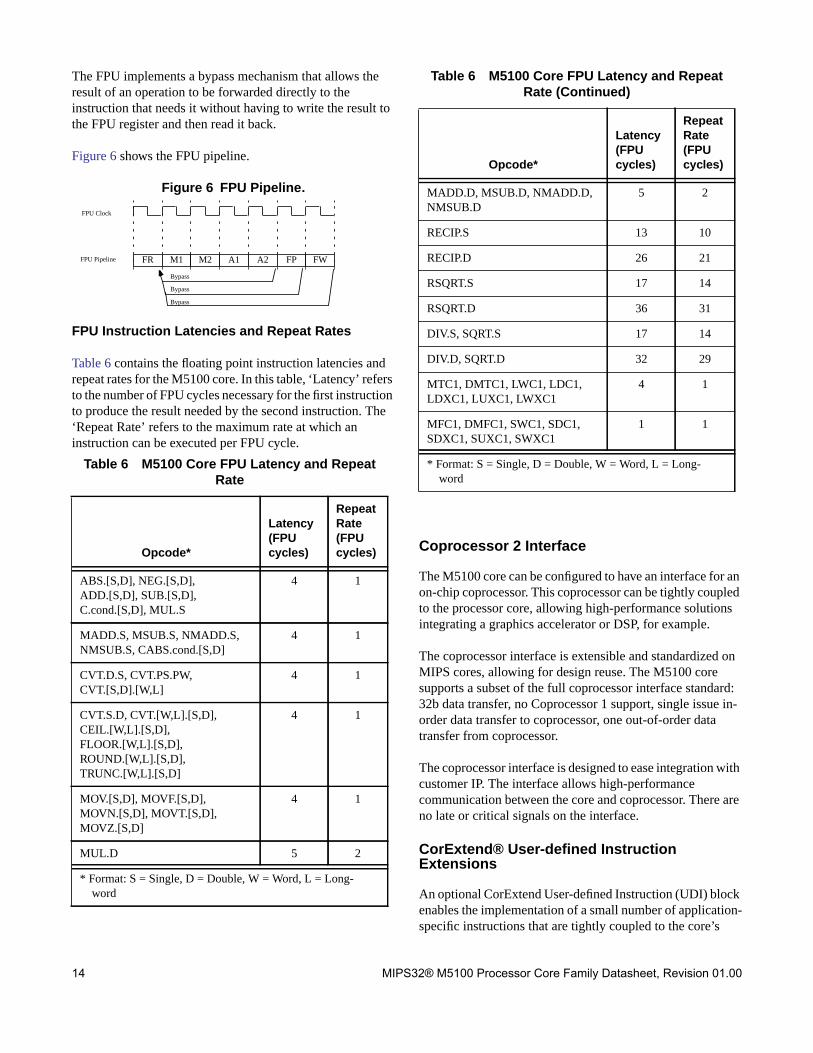
The FPU implements a bypass mechanism that allows theresult of an operation to be forwarded directly to theinstruction that needs it without having to write the result tothe FPU register and then read it back.
Figure 6 shows the FPU pipeline.
Figure 6 FPU Pipeline.
FPU Instruction Latencies and Repeat Rates
Table 6 contains the floating point instruction latencies andrepeat rates for the M5100 core. In this table, ‘Latency’ refersto the number of FPU cycles necessary for the first instructionto produce the result needed by the second instruction. The‘Repeat Rate’ refers to the maximum rate at which aninstruction can be executed per FPU cycle.
Coprocessor 2 Interface
The M5100 core can be configured to have an interface for anon-chip coprocessor. This coprocessor can be tightly coupledto the processor core, allowing high-performance solutionsintegrating a graphics accelerator or DSP, for example.
The coprocessor interface is extensible and standardized onMIPS cores, allowing for design reuse. The M5100 coresupports a subset of the full coprocessor interface standard:32b data transfer, no Coprocessor 1 support, single issue in-order data transfer to coprocessor, one out-of-order datatransfer from coprocessor.
The coprocessor interface is designed to ease integration withcustomer IP. The interface allows high-performancecommunication between the core and coprocessor. There areno late or critical signals on the interface.
CorExtend® User-defined InstructionExtensions
An optional CorExtend User-defined Instruction (UDI) blockenables the implementation of a small number of application-specific instructions that are tightly coupled to the core’s
Table 6 M5100 Core FPU Latency and RepeatRate
Opcode*
Latency(FPUcycles)
RepeatRate(FPUcycles)
ABS.[S,D], NEG.[S,D],ADD.[S,D], SUB.[S,D],C.cond.[S,D], MUL.S
4 1
MADD.S, MSUB.S, NMADD.S,NMSUB.S, CABS.cond.[S,D]
4 1
CVT.D.S, CVT.PS.PW,CVT.[S,D].[W,L]
4 1
CVT.S.D, CVT.[W,L].[S,D],CEIL.[W,L].[S,D],FLOOR.[W,L].[S,D],ROUND.[W,L].[S,D],TRUNC.[W,L].[S,D]
4 1
MOV.[S,D], MOVF.[S,D],MOVN.[S,D], MOVT.[S,D],MOVZ.[S,D]
4 1
MUL.D 5 2
* Format: S = Single, D = Double, W = Word, L = Long-word
FR M1 M2 A1 A2 FP FWFPU Pipeline
Bypass
Bypass
Bypass
FPU Clock
MADD.D, MSUB.D, NMADD.D,NMSUB.D
5 2
RECIP.S 13 10
RECIP.D 26 21
RSQRT.S 17 14
RSQRT.D 36 31
DIV.S, SQRT.S 17 14
DIV.D, SQRT.D 32 29
MTC1, DMTC1, LWC1, LDC1,LDXC1, LUXC1, LWXC1
4 1
MFC1, DMFC1, SWC1, SDC1,SDXC1, SUXC1, SWXC1
1 1
Table 6 M5100 Core FPU Latency and RepeatRate (Continued)
Opcode*
Latency(FPUcycles)
RepeatRate(FPUcycles)
* Format: S = Single, D = Double, W = Word, L = Long-word
MIPS32® M5100 Processor Core Family Datasheet, Revision 01.00 15
execution unit. The interface to the UDI block is external tothe M5100 core.
Such instructions may operate on a general-purpose register,immediate data specified by the instruction word, or localstate stored within the UDI block. The destination may be ageneral-purpose register or local UDI state. The operationmay complete in one cycle or multiple cycles, if desired.
Anti-Tamper Security Features
The core provides security features that counter side-channelattacks attempting to reveal the code or data running on theprocessor.
Random slips can be generated in order to disguise the timingand power profile of an algorithm executing on the processor.This reduces the core’s vulnerability to side channel attacks.Power management techniques are used to ensure that thepower profile of a random slip is indistinguishable from thepower profile of the executing instructions.
The core contains a general-purpose pseudo generator for useby software. The generator may optionally be designed by theimplementor of the core, thus allowing the quality of thepseudo random number sequences to be suited for any needs.
EJTAG Debug Support
The M5100 core provides for an optional Enhanced JTAG(EJTAG) interface for use in the software debug ofapplication and kernel code. In addition to standard usermode and kernel modes of operation, the M5100 coreprovides a Debug mode that is entered after a debug exception(derived from a hardware breakpoint, single-step exception,etc.) is taken and continues until a debug exception return(DERET) instruction is executed. During this time, theprocessor executes the debug exception handler routine.
The EJTAG interface operates through the Test Access Port(TAP), a serial communication port used for transferring testdata in and out of the M5100 core. In addition to the standardJTAG instructions, special instructions defined in the EJTAGspecification specify which registers are selected and howthey are used.
Debug Registers
Four debug registers (DEBUG, DEBUG2, DEPC, and DESAVE)have been added to the MIPS Coprocessor 0 (CP0) registerset. The DEBUG and DEBUG2 registers show the cause of thedebug exception and are used for setting up single-stepoperations. The DEPC (Debug Exception Program Counter)register holds the address on which the debug exception wastaken, which is used to resume program execution after the
debug operation finishes. Finally, the DESAVE (DebugException Save) register enables the saving of general-purpose registers used during execution of the debugexception handler.
To exit debug mode, a Debug Exception Return (DERET)instruction is executed. When this instruction is executed, thesystem exits debug mode, allowing normal execution ofapplication and system code to resume.
EJTAG Hardware Breakpoints
There are several types of simple hardware breakpointsdefined in the EJTAG specification. These stop the normaloperation of the CPU and force the system into debug mode.There are two types of simple hardware breakpointsimplemented in the M5100 core: Instruction breakpoints andData breakpoints. Additionally, complex hardwarebreakpoints can be included, which allow detection of moreintricate sequences of events.
The M5100 core can be configured with the followingbreakpoint options:
• No data or instruction, or complex breakpoints
• One data and two instruction breakpoints, withoutcomplex breakpoints
• Two data and four instruction breakpoints, withoutcomplex breakpoints
• Two data and six instruction breakpoints, with or withoutcomplex breakpoints
• Four data and eight instruction breakpoints, with orwithout complex breakpoints
Instruction breakpoints occur on instruction executionoperations, and the breakpoint is set on the virtual address. Amask can be applied to the virtual address to set breakpointson a binary range of instructions.
Data breakpoints occur on load/store transactions, and thebreakpoint is set on a virtual address value, with the samesingle address or binary address range as the Instructionbreakpoint. Data breakpoints can be set on a load, a store, orboth. Data breakpoints can also be set to match on theoperand value of the load/store operation, with byte-granularity masking. Finally, masks can be applied to boththe virtual address and the load/store value.
In addition, the M5100 core has a configurable feature tosupport data and instruction address-range triggeredbreakpoints, where a breakpoint can occur when a virtualaddress is either within or outside a pair of 32-bit addresses.Unlike the traditional address-mask control, address-range
16 MIPS32® M5100 Processor Core Family Datasheet, Revision 01.00
triggering is not restricted to a power-of-two binaryboundary.
Complex breakpoints utilize the simple instruction and databreakpoints and break when combinations of events are seen.Complex break features include:
• Pass Counters - Each time a matching condition is seen, acounter is decremented. The break or trigger will only beenabled when the counter has counted down to 0.
• Tuples - A tuple is the pairing of an instruction and adata breakpoint. The tuple will match if both the virtualaddress of the load or store instruction matches theinstruction breakpoint, and the data breakpoint of theresulting load or store address and optional data valuematches.
• Priming - This allows a breakpoint to be enabled onlyafter other break conditions have been met. Also calledsequential or armed triggering.
• Qualified - This feature uses a data breakpoint to qualifywhen an instruction breakpoint can be taken. Once a loadmatches the data address and the data value, theinstruction break will be enabled. If a load matches theaddress, but has mis-matching data, the instruction breakwill be disabled.
Performance Counters
Performance counters are used to accumulate occurrences ofinternal predefined events/cycles/conditions for programanalysis, debug, or profiling. A few examples of event typesare clock cycles, instructions executed, specific instructiontypes executed, loads, stores, exceptions, and cycles while theCPU is stalled. There are two, 32-bit counters. Each can countone of the 64 internal predefined events selected by acorresponding control register. A counter overflow can beprogrammed to generate an interrupt, where the interrupthandler software can maintain larger total counts.
PC/Address Sampling
This sampling function is used for program profiling and hot-spots analysis. Instruction PC and/or Load/Store addressescan be sampled periodically. The result is scanned outthrough the EJTAG port. The Debug Control Register (DCR)is used to specify the sample period and the sample trigger.
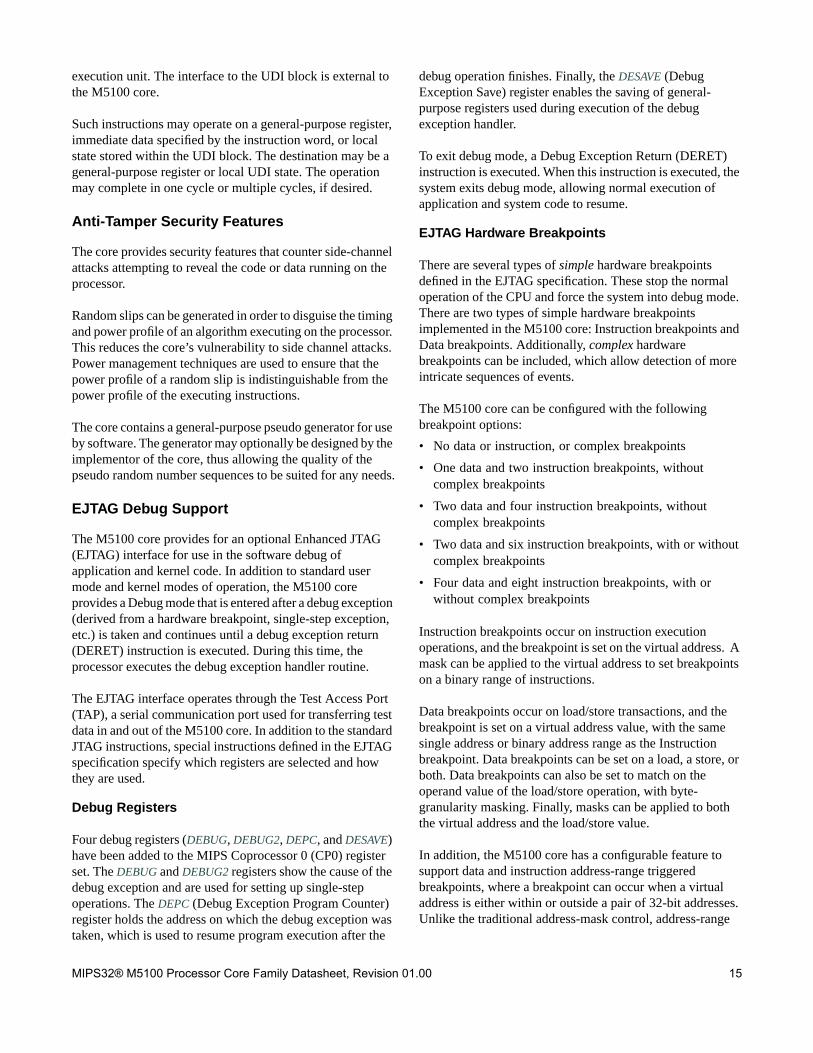
Fast Debug Channel (FDC)
The M5100 core includes optional FDC as a mechanism forhigh bandwidth data transfer between a debug host/probe anda target. FDC provides a FIFO buffering scheme to transfer
data serially, with low CPU overhead and minimized waitingtime. The data transfer occurs in the background, and thetarget CPU can either choose to check the status of thetransfer periodically, or it can choose to be interrupted at theend of the transfer.
Figure 7 FDC Overview
iFlowtrace™
The M5100 core has an option for a simple trace mechanismcalled iFlowtrace. This mechanism only traces the instructionPC, not data addresses or values. This simplification allowsthe trace block to be smaller and the trace compression to bemore efficient. iFlowtrace memory can be configured as off-chip, on-chip, or both.
iFlowtrace also offers special-event trace modes whennormal tracing is disabled, namely:
• Function Call/Return and Exception Tracing mode totrace the PC value of function calls and returns and/orexceptions and returns.
• Breakpoint Match mode traces the breakpoint ID of amatching breakpoint and, for data breakpoints, the PCvalue of the instruction that caused it.
• Filtered Data Tracing mode traces the ID of a matchingdata breakpoint, the load or store data value, access typeand memory access size, and the low-order address bitsof the memory access, which is useful when the databreakpoint is set up to match a binary range of addresses.
• User Trace Messages. The user can instrument their codeto add their own 32-bit value messages into the trace bywriting to the Cop0 UTM register.
• Delta Cycle mode works in combination with the abovetrace modes to provide a timestamp between storedevents. It reports the number of cycles that have elapsedsince the last message was generated and put into thetrace.
M5100ProbeEJTAG
TAP
FDC
Tap Controller
TDI
TDO
TMS
FIFOReceive fromProbe to Core
Transmit fromCore to Probe FIFO
32
32
MIPS32® M5100 Processor Core Family Datasheet, Revision 01.00 17
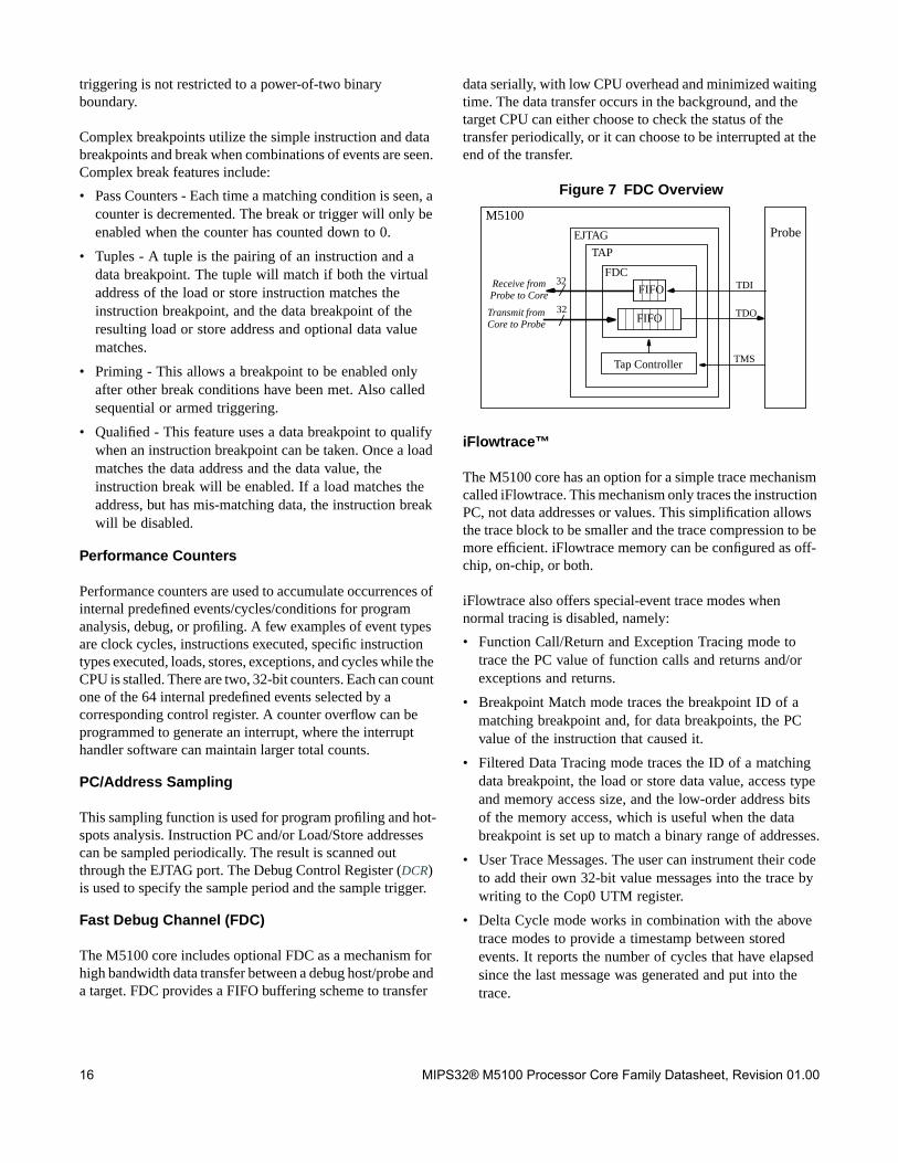
cJTAG Support
The M5100 core provides an external conversion block whichconverts the existing EJTAG (IEEE 1149.1) 4-wire interfaceat the M5100 core to a cJTAG (IEEE 1149.7) 2-wireinterface. cJTAG reduces the number of wires from 4 to 2 andenables the support of Star-2 scan topology in the systemdebug environment.
Figure 8 cJTAG Support
SecureDebug
SecureDebug improves security by disabling untrustedEJTAG debug access. An input signal is used to disabledebug features, such as Probe Trap, Debug InterruptException (EjtagBrk and DINT), EJTAGBOOT instruction,and PC Sampling.
Testability
Testability for production testing of the core is supportedthrough the use of internal scan and memory BIST.
Internal Scan
Full mux-based scan for maximum test coverage issupported, with a configurable number of scan chains. ATPGtest coverage can exceed 99%, depending on standard celllibraries and configuration options.
Memory BIST
Memory BIST for the on-chip trace memory is optional.
Memory BIST can be inserted with a CAD tool or other user-specified method. Wrapper modules and special side-bandsignal buses of configurable width are provided within thecore to facilitate this approach.
Build-Time Configuration Options
The M5100 core allows a number of features to becustomized based on the intended application. Table 7summarizes the key configuration options that can be selectedwhen the core is synthesized and implemented.
For a core that has already been built, software can determinethe value of many of these options by checking an appropriateregister field. Refer to the MIPS32® M5100 Processor CoreFamily Software User’s Manual for a more completedescription of these fields. The value of some options that donot have a functional effect on the core are not visible tosoftware.
TapController
M5100
EJTAGEJTAG4-wire
interface
TDITDOTCKTMS
TMSCTCK
cJTAGConversion
Block
cJTAG2-wire
interface
Table 7 Build-time Configuration Options
Option Choices Software Visibility
Integer register file sets 1, 2, 4, 8 or 16 SRSCtlHSS
Integer register file implementation style Flops or generator N/A
Virtualization number of guests 1, 2, 3, 4, 5, 6, 7 N/A
ISA support MIPS32 only, ormicroMIPS only, orMIPS32 and microMIPS present
Config3ISA
DSP Module Present or not Config3DSPP, Config3DSP2P
Multiply/divide implementation style High performance or min area (if DSP is not present) ConfigMDU
Floating-point Unit Present or not Config1FP
* These bits indicate the presence of an external block. Bits will not be set if interface is present, but block is not.
18 MIPS32® M5100 Processor Core Family Datasheet, Revision 01.00
Revision History
Adder implementation style Structured or Simple N/A
EJTAG TAP controller Present or not N/A
EJTAG TAP Fast Debug Channel (FDC) Present or not (even when TAP is present) DCRFDCI
EJTAG TAP FDC FIFO size Two TX/two RX, or eight TX/four RX 32-bit registers FDCFG
Instruction/data hardware breakpoints 0/0, 2/1, 4/2, 6/2, or 8/4 DCRInstBrk, IBSBCN
DCRDataBrk, DBSBCN
Hardware breakpoint trigger by Address match, orAddress match and address range
IBCnhwart, DBCnhwart
Complex breakpoints 0/0, 6/2, or 8/4 DCRCBT
Performance Counters Present or not Config1PC
iFlowtrace hardware Present or not Config3ITL
iFlowtrace memory location On-core or off-chip IFCTLofc
iFlowtrace on-chip memory size 256B - 8MB N/A
CorExtend interface Present or not ConfigUDI*
Coprocessor2 interface Present or not Config1C2*
SRAM interface style Separate instruction/data or unified ConfigDS
SRAM Parity Present or not ErrCtlPE
Interrupt synchronizers Present or not N/A
Interrupt Vector Offset Compute from Vector Input or Immediate Offset N/A
Clock gating Top-level, integer register file array, fine-grain, or none N/A
PC Sampling Present or not Debug Control Register
Data Address Sampling Present or not Debug Control Register
PRID User defined Processor Identification PRIDCompanyOpt
Table 7 Build-time Configuration Options (Continued)
Option Choices Software Visibility
* These bits indicate the presence of an external block. Bits will not be set if interface is present, but block is not.
Revision Date Description
01.00 December 31, 2013 • Initial 1_0_0 release.

Unpublished rights (if any) reserved under the copyright laws of the United States of America and other countries. This document contains information that is proprietary to MIPS Tech, LLC, a Wave Computing company (“MIPS”) and MIPS’ affiliates as applicable. Any copying, reproducing, modifying or use of this information (in whole or in part) that is not expressly permitted in writing by MIPS or MIPS’ affiliates as applicable or an authorized third party is strictly prohibited. At a minimum, this information is protected under unfair competition and copyright laws. Violations thereof may result in criminal penalties and fines. Any document provided in source format (i.e., in a modifiable form such as in FrameMaker or Microsoft Word format) is subject to use and distribution restrictions that are independent of and supplemental to any and all confidentiality restrictions. UNDER NO CIRCUMSTANCES MAY A DOCUMENT PROVIDED IN SOURCE FORMAT BE DISTRIBUTED TO A THIRD PARTY IN SOURCE FORMAT WITHOUT THE EXPRESS WRITTEN PERMISSION OF MIPS (AND MIPS’ AFFILIATES AS APPLICABLE) reserve the right to change the information contained in this document to improve function, design or otherwise. MIPS and MIPS’ affiliates do not assume any liability arising out of the application or use of this information, or of any error or omission in such information. Any warranties, whether express, statutory, implied or otherwise, including but not limited to the implied warranties of merchantability or fitness for a particular purpose, are excluded. Except as expressly provided in any written license agreement from MIPS or an authorized third party, the furnishing of this document does not give recipient any license to any intellectual property rights, including any patent rights, that cover the information in this document. The information contained in this document shall not be exported, reexported, transferred, or released, directly or indirectly, in violation of the law of any country or international law, regulation, treaty, Executive Order, statute, amendments or supplements thereto. Should a conflict arise regarding the export, reexport, transfer, or release of the information contained in this document, the laws of the United States of America shall be the governing law. The information contained in this document constitutes one or more of the following: commercial computer software, commercial computer software documentation or other commercial items. If the user of this information, or any related documentation of any kind, including related technical data or manuals, is an agency, department, or other entity of the United States government ("Government"), the use, duplication, reproduction, release, modification, disclosure, or transfer of this information, or any related documentation of any kind, is restricted in accordance with Federal Acquisition Regulation 12.212 for civilian agencies and Defense Federal Acquisition Regulation Supplement 227.7202 for military agencies. The use of this information by the Government is further restricted in accordance with the terms of the license agreement(s) and/or applicable contract terms and conditions covering this information from MIPS Technologies or an authorized third party. MIPS, MIPS I, MIPS II, MIPS III, MIPS IV, MIPS V, MIPSr3, MIPS32, MIPS64, microMIPS32, microMIPS64, MIPS-3D, MIPS16, MIPS16e, MIPS-Based, MIPSsim, MIPSpro, MIPS-VERIFIED, Aptiv logo, microAptiv logo, interAptiv logo, microMIPS logo, MIPS Technologies logo, MIPS-VERIFIED logo, proAptiv logo, 4K, 4Kc, 4Km, 4Kp, 4KE, 4KEc, 4KEm, 4KEp, 4KS, 4KSc, 4KSd, M4K, M14K, 5K, 5Kc, 5Kf, 24K, 24Kc, 24Kf, 24KE, 24KEc, 24KEf, 34K, 34Kc, 34Kf, 74K, 74Kc, 74Kf, 1004K, 1004Kc, 1004Kf, 1074K, 1074Kc, 1074Kf, R3000, R4000, R5000, Aptiv, ASMACRO, Atlas, "At the core of the user experience.", BusBridge, Bus Navigator, CLAM, CorExtend, CoreFPGA, CoreLV, EC, FPGA View, FS2, FS2 FIRST SILICON SOLUTIONS logo, FS2 NAVIGATOR, HyperDebug, HyperJTAG, IASim, iFlowtrace, interAptiv, JALGO, Logic Navigator, Malta, MDMX, MED, MGB, microAptiv, microMIPS, Navigator, OCI, PDtrace, the Pipeline, proAptiv, Pro Series, SEAD-3, SmartMIPS, SOC-it, and YAMON are trademarks or registered trademarks of MIPS and MIPS’ affiliates as applicable in the United States and other countries. All other trademarks referred to herein are the property of their respective owners. мф aLt{онϯ aрмлл tNJƻŎŜǎǎƻNJ /ƻNJŜ CŀƳƛƭȅ 5ŀǘŀǎƘŜŜǘΣ wŜǾƛǎƛƻƴ лмΦлл
Copyright © Wave Computing, Inc. All rights reserved. www.wavecomp.ai
Saraj.Mudigonda
Typewritten Text