MIPS in Verilog Lecture 1 · MIPS Architecture Example: subset of MIPS processor architecture –...
28
CMOS VLSI Design Verilog & MIPS0: Slide 1 Verilog & MIPS0: Slide 1 Introduction to CMOS VLSI Design MIPS in Verilog Lecture 1 Lecture by Peter Kogge Fall 2009, 2010 University of Notre Dame Using slides by Jay Brockman Notre Dame 2008, and David Harris, Harvey Mudd College http://www.cmosvlsi.com/coursematerials.html
Transcript of MIPS in Verilog Lecture 1 · MIPS Architecture Example: subset of MIPS processor architecture –...

CMOS VLSI DesignVerilog & MIPS0: Slide 1Verilog & MIPS0: Slide 1
Introduction toCMOS VLSI
Design
MIPS in VerilogLecture 1
Lecture by Peter KoggeFall 2009, 2010
University of Notre DameUsing slides by Jay Brockman Notre Dame 2008,
and David Harris, Harvey Mudd Collegehttp://www.cmosvlsi.com/coursematerials.html

CMOS VLSI DesignVerilog & MIPS0: Slide 2Verilog & MIPS0: Slide 2Slide 2
MIPS ArchitectureExample: subset of MIPS processor architecture– Drawn from Patterson & Hennessy
MIPS is a 32-bit architecture with 32 registers– Consider 8-bit subset using 8-bit datapath– Only implement 8 registers ($0 - $7)– $0 hardwired to 00000000– 8-bit program counter
David Harris has developed labs to implement– Uses Electric CAD tools– Illustrate the key concepts in VLSI design

CMOS VLSI DesignVerilog & MIPS0: Slide 3Verilog & MIPS0: Slide 3Slide 3
Instruction Set

CMOS VLSI DesignVerilog & MIPS0: Slide 4Verilog & MIPS0: Slide 4Slide 4
Instruction Encoding32-bit instruction encoding– Requires four cycles to fetch on 8-bit datapath
format example encoding
R
I
J
0 ra rb rd 0 funct
op
op
ra rb imm
6
6
6
65 5 5 5
5 5 16
26
add $rd, $ra, $rb
beq $ra, $rb, imm
j dest dest
CMOS VLSI DesignVerilog & MIPS0: Slide 5Verilog & MIPS0: Slide 5Slide 5
Fibonacci (C)f0 = 1; f-1 = -1fn = fn-1 + fn-2
f = 1, 1, 2, 3, 5, 8, 13, …

CMOS VLSI DesignVerilog & MIPS0: Slide 6Verilog & MIPS0: Slide 6Slide 6
Fibonacci (Assembly)1st statement: n = 8How do we translate this to assembly?

CMOS VLSI DesignVerilog & MIPS0: Slide 7Verilog & MIPS0: Slide 7Slide 7
Fibonacci (Assembly)
CMOS VLSI DesignVerilog & MIPS0: Slide 8Verilog & MIPS0: Slide 8Slide 8
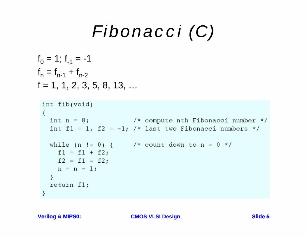
Fibonacci (Binary)1st statement: addi $3, $0, 8How do we translate this to machine language?– Hint: use instruction encodings below
format example encoding
R
I
J
0 ra rb rd 0 funct
op
op
ra rb imm
6
6
6
65 5 5 5
5 5 16
26
add $rd, $ra, $rb
beq $ra, $rb, imm
j dest dest

CMOS VLSI DesignVerilog & MIPS0: Slide 9Verilog & MIPS0: Slide 9Slide 9
Fibonacci (Binary)Machine language program

CMOS VLSI DesignVerilog & MIPS0: Slide 10Verilog & MIPS0: Slide 10Slide 10
MIPS MicroarchitectureMulticycle μarchitecture from Patterson & Hennessy
PCMux
0
1
RegistersWriteregister
Writedata
Readdata 1
Readdata 2
Readregister 1
Readregister 2
Instruction[15: 11]
Mux
0
1
Mux
0
1
1
Instruction[7: 0]
Instruction[25 : 21]
Instruction[20 : 16]
Instruction[15 : 0]
Instructionregister
ALUcontrol
ALUresult
ALUZero
Memorydata
register
A
B
IorD
MemRead
MemWrite
MemtoReg
PCWriteCond
PCWrite
IRWrite[3:0]
ALUOp
ALUSrcB
ALUSrcA
RegDst
PCSource
RegWriteControl
Outputs
Op[5 : 0]
Instruction[31:26]
Instruction [5 : 0]
Mux
0
2
JumpaddressInstruction [5 : 0] 6 8
Shiftleft 2
1
1 Mux
0
32
Mux
0
1ALUOut
MemoryMemData
Writedata
Address
PCEn
ALUControl

CMOS VLSI DesignVerilog & MIPS0: Slide 11Verilog & MIPS0: Slide 11Slide 11
Multicycle Controller
PCWritePCSource = 10
ALUSrcA = 1ALUSrcB = 00ALUOp = 01PCWriteCond
PCSource = 01
ALUSrcA =1ALUSrcB = 00ALUOp= 10
RegDst = 1RegWrite
MemtoReg = 0MemWriteIorD = 1
MemReadIorD = 1
ALUSrcA = 1ALUSrcB = 10ALUOp = 00
RegDst= 0RegWrite
MemtoReg =1
ALUSrcA = 0ALUSrcB = 11ALUOp = 00
MemReadALUSrcA = 0
IorD = 0IRWrite3
ALUSrcB = 01ALUOp = 00
PCWritePCSource = 00
Instruction fetch
Instruction decode/register fetch
Jumpcompletion
BranchcompletionExecution
Memory addresscomputation
Memoryaccess
Memoryaccess R-type completion
Write-back step
(Op = 'LB ') or (Op = 'SB ') (Op = R-type)
(Op = 'B
EQ')
(Op
='J
')
(Op = 'SB')
(Op
='L
B')
7
0
4
121195
1086
Reset
MemReadALUSrcA = 0
IorD = 0IRWrite2
ALUSrcB = 01ALUOp = 00
PCWritePCSource = 00
1MemRead
ALUSrcA = 0IorD = 0IRWrite1
ALUSrcB = 01ALUOp = 00
PCWritePCSource = 00
2MemRead
ALUSrcA = 0IorD = 0IRWrite0
ALUSrcB = 01ALUOp = 00
PCWritePCSource = 00
3

CMOS VLSI DesignVerilog & MIPS0: Slide 12Verilog & MIPS0: Slide 120: Introduction Slide 12
Logic DesignStart at top level– Hierarchically decompose MIPS into units
Top-level interface
reset
ph1
ph2
crystaloscillator
2-phaseclockgenerator MIPS
processor adr
writedata
memdata
externalmemory
memreadmemwrite
8
8
8
CMOS VLSI DesignVerilog & MIPS0: Slide 13Verilog & MIPS0: Slide 13Slide 13
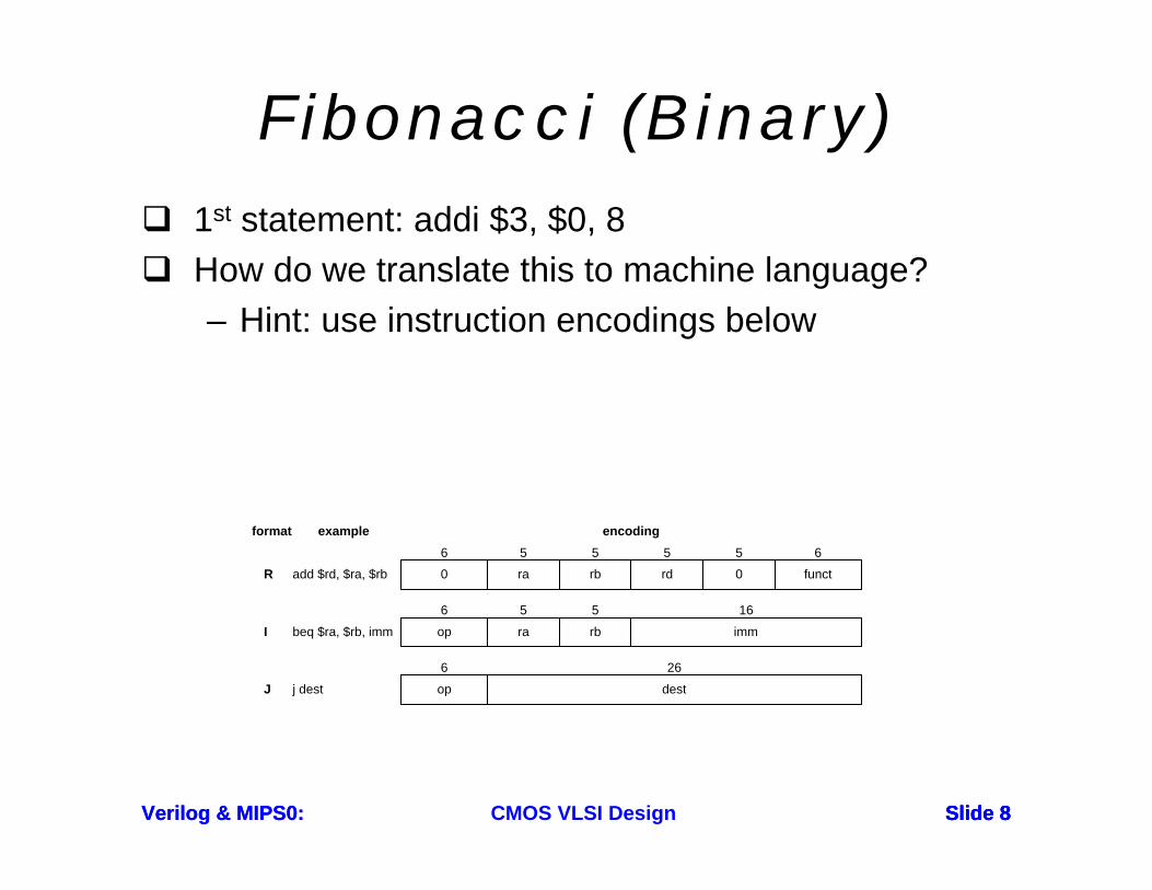
Block Diagram
datapath
controlleralucontrol
ph1
ph2
reset
memdata[7:0]
writedata[7:0]
adr[7:0]
memread
memwrite
op[5:0]
zero
pcen
regwrite
irwrite[3:0]
mem
toreg
iord
pcsource[1:0]
alusrcb[1:0]
alusrca
aluop[1:0]
regdst
funct[5:0]
alucontrol[2:0]
PCMux
0
1
RegistersWriteregister
Writedata
Readdata 1
Readdata 2
Readregister 1
Readregister 2
Instruction[15: 11]
Mux
0
1
Mux
0
1
1
Instruction[7: 0]
Instruction[25 : 21]
Instruction[20 : 16]
Instruction[15 : 0]
Instructionregister
ALUcontrol
ALUresult
ALUZero
Memorydata
register
A
B
IorD
MemRead
MemWrite
MemtoReg
PCWriteCond
PCWrite
IRWrite[3:0]
ALUOp
ALUSrcB
ALUSrcA
RegDst
PCSource
RegWriteControl
Outputs
Op[5 : 0]
Instruction[31:26]
Instruction [5 : 0]
Mux
0
2
JumpaddressInstruction [5 : 0] 6 8
Shiftleft 2
1
1 Mux
0
32
Mux
0
1ALUOut
MemoryMemData
Writedata
Address
PCEn
ALUControl

CMOS VLSI DesignVerilog & MIPS0: Slide 14Verilog & MIPS0: Slide 14Slide 14
Hierarchical Designmips
controller alucontrol datapath
standardcell library
bitslice zipper
alu
and2
flopinv4x
mux2
mux4
ramslice
fulladder
nand2nor2
or2
inv
tri

CMOS VLSI DesignVerilog & MIPS0: Slide 15Verilog & MIPS0: Slide 15Slide 15
Physical DesignFloorplanStandard cells– Place & route
Datapaths– Slice planning
Area estimation
CMOS VLSI DesignVerilog & MIPS0: Slide 16Verilog & MIPS0: Slide 16Slide 16
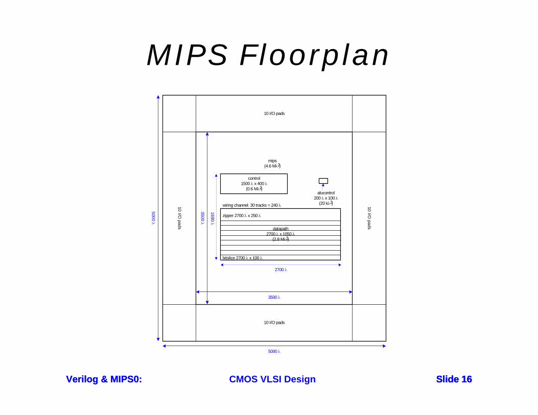
MIPS Floorplan
datapath2700 λ x 1050 λ
(2.8 Mλ2)
alucontrol200 λ x 100 λ
(20 kλ2)
zipper 2700 λ x 250 λ
2700 λ
1690 λ
wiring channel: 30 tracks = 240 λ
mips(4.6 Mλ2)
bitslice 2700 λ x 100 λ
control1500 λ x 400 λ
(0.6 Mλ2)
3500 λ
3500 λ
5000λ
5000 λ
10 I/O pads
10 I/O pads
10 I/O pads
10 I/O pads

CMOS VLSI DesignVerilog & MIPS0: Slide 17Verilog & MIPS0: Slide 17Slide 17
MIPS Layout

CMOS VLSI DesignVerilog & MIPS0: Slide 18Verilog & MIPS0: Slide 18Slide 18
Standard CellsUniform cell heightUniform well heightM1 VDD and GND railsM2 Access to I/OsWell / substrate tapsExploits regularity
CMOS VLSI DesignVerilog & MIPS0: Slide 19Verilog & MIPS0: Slide 19Slide 19
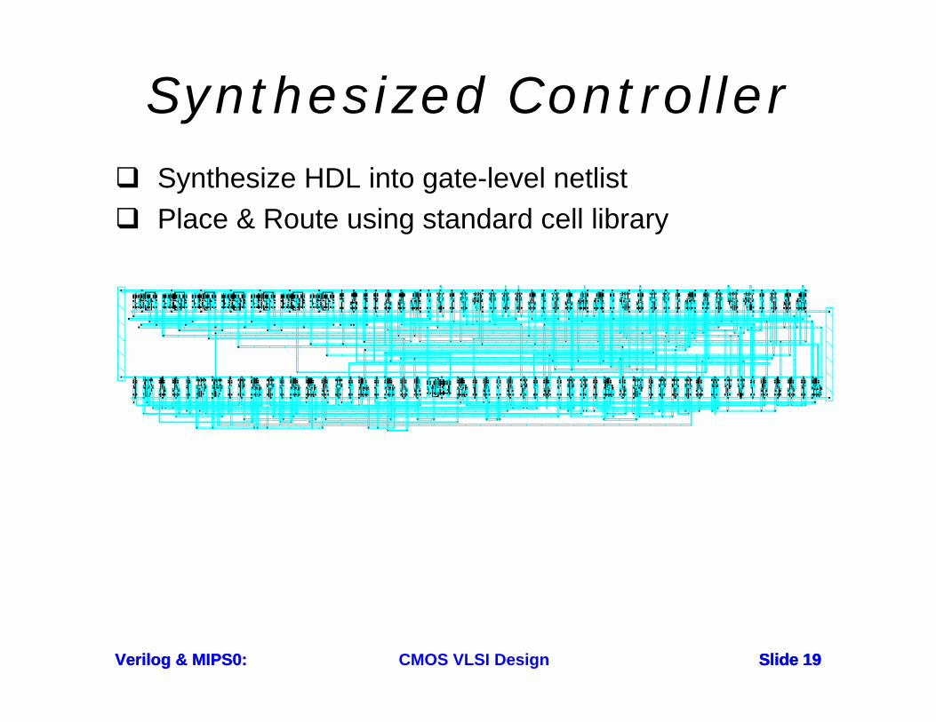
Synthesized ControllerSynthesize HDL into gate-level netlistPlace & Route using standard cell library

CMOS VLSI DesignVerilog & MIPS0: Slide 20Verilog & MIPS0: Slide 20Slide 20
MIPS DatapathMulticycle μarchitecture from Patterson & Hennessy
PCMux
0
1
RegistersWriteregister
Writedata
Readdata 1
Readdata 2
Readregister 1
Readregister 2
Instruction[15: 11]
Mux
0
1
Mux
0
1
1
Instruction[7: 0]
Instruction[25 : 21]
Instruction[20 : 16]
Instruction[15 : 0]
Instructionregister
ALUcontrol
ALUresult
ALUZero
Memorydata
register
A
B
IorD
MemRead
MemWrite
MemtoReg
PCWriteCond
PCWrite
IRWrite[3:0]
ALUOp
ALUSrcB
ALUSrcA
RegDst
PCSource
RegWriteControl
Outputs
Op[5 : 0]
Instruction[31:26]
Instruction [5 : 0]
Mux
0
2
JumpaddressInstruction [5 : 0] 6 8
Shiftleft 2
1
1 Mux
0
32
Mux
0
1ALUOut
MemoryMemData
Writedata
Address
PCEn
ALUControl
CMOS VLSI DesignVerilog & MIPS0: Slide 21Verilog & MIPS0: Slide 21Slide 21
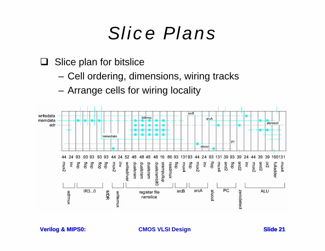
Slice PlansSlice plan for bitslice– Cell ordering, dimensions, wiring tracks– Arrange cells for wiring locality
CMOS VLSI DesignVerilog & MIPS0: Slide 22Verilog & MIPS0: Slide 22Slide 22
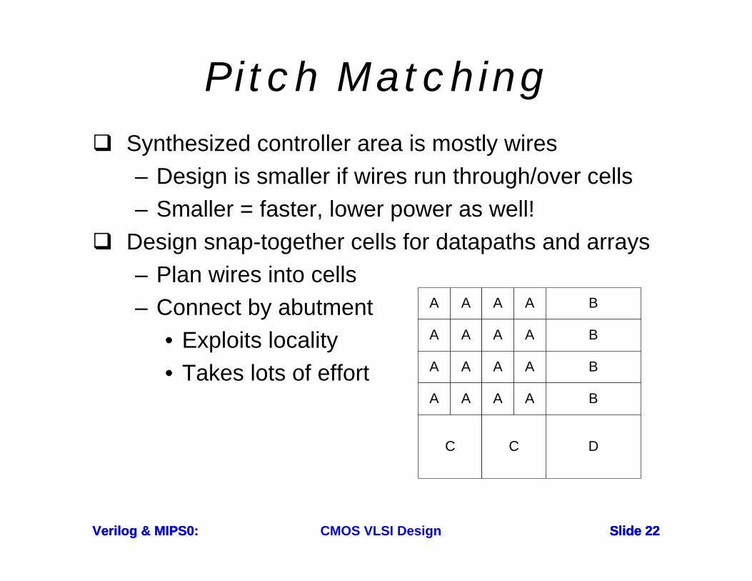
Pitch MatchingSynthesized controller area is mostly wires– Design is smaller if wires run through/over cells– Smaller = faster, lower power as well!
Design snap-together cells for datapaths and arrays– Plan wires into cells– Connect by abutment
• Exploits locality• Takes lots of effort
A A A A
A A A A
A A A A
A A A A
B
B
B
B
C C D
CMOS VLSI DesignVerilog & MIPS0: Slide 23Verilog & MIPS0: Slide 23Slide 23
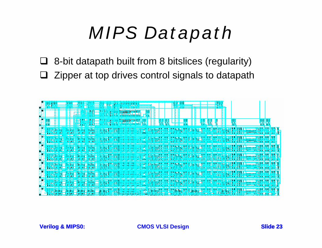
MIPS Datapath8-bit datapath built from 8 bitslices (regularity)Zipper at top drives control signals to datapath

CMOS VLSI DesignVerilog & MIPS0: Slide 24Verilog & MIPS0: Slide 24Slide 24
MIPS ALUArithmetic / Logic Unit is part of bitslice
CMOS VLSI DesignVerilog & MIPS0: Slide 25Verilog & MIPS0: Slide 25Slide 25
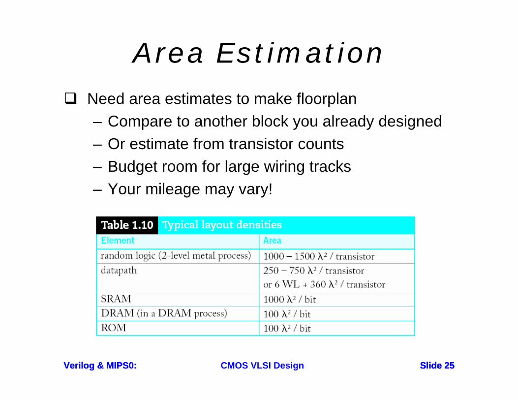
Area EstimationNeed area estimates to make floorplan– Compare to another block you already designed– Or estimate from transistor counts– Budget room for large wiring tracks– Your mileage may vary!

CMOS VLSI DesignVerilog & MIPS0: Slide 26Verilog & MIPS0: Slide 26Slide 26
Design VerificationFabrication is slow & expensive– MOSIS 0.6μm: $1000, 3 months– State of art: $1M, 1 month
Debugging chips is very hard– Limited visibility into operation
Prove design is right before building!– Logic simulation– Ckt. simulation / formal verification– Layout vs. schematic comparison– Design & electrical rule checks
Verification is > 50% of effort on most chips!
Specification
ArchitectureDesign
LogicDesign
CircuitDesign
PhysicalDesign
=
=
=
=
Function
Function
Function
FunctionTimingPower
CMOS VLSI DesignVerilog & MIPS0: Slide 27Verilog & MIPS0: Slide 27Slide 27
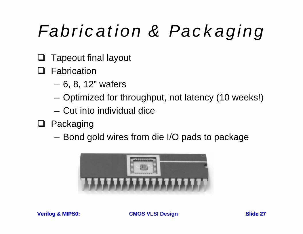
Fabrication & PackagingTapeout final layoutFabrication– 6, 8, 12” wafers– Optimized for throughput, not latency (10 weeks!)– Cut into individual dice
Packaging– Bond gold wires from die I/O pads to package
CMOS VLSI DesignVerilog & MIPS0: Slide 28Verilog & MIPS0: Slide 28Slide 28
TestingTest that chip operates– Design errors– Manufacturing errors
A single dust particle or wafer defect kills a die– Yields from 90% to < 10%– Depends on die size, maturity of process– Test each part before shipping to customer