Minimum Thermal Conductivity in Weak Topological Insulators … Mini… · · 2016-06-05Minimum...
8
FULL PAPER © 2016 WILEY-VCH Verlag GmbH & Co. KGaA, Weinheim 1 wileyonlinelibrary.com formidable endeavors. [7–9] Distinct from the normal insulators (NIs), TIs exhibit nontrivial gapless surface states that are topologically protected against scattering by time-reversal symmetry. [10–12] There has been growing interest in improving the TE performance of TIs by taking advantage of their distinctive electronic states. [13–17] The theoretical investigation on Bi 2 Te 3 and Bi 2 Se 3 TIs thin films suggested that enhanced electrical conductivity and Seebeck coefficient can be simultane- ously realized by tuning the hybridiza- tion gap of surface states. [16] Recent work has theoretically predicted that the strong energy-dependent electron scattering of the surface states could lead to large See- beck coefficient. [17] These advances in the surface states of TIs imply their potential use as promising TE materials. Neverthe- less, other intrinsic connections between TIs and TEs, particularly with respect to lattice dynamics and related phonon-transport properties are still primitive and need further development. Ideally a TE material can achieve its optimum performance when the lattice thermal conductivity (κ l ) is reduced to its lowest value—the minimum thermal conductivity (MTC), [18] which occurs when the phonons have mean free paths on the order of one-phonon wavelength. [19] It is however very unusual for a crystalline material to achieve the MTC at room tempera- ture. [20,21] For TIs, the heavy constituents are favorable for low κ l but these alone cannot lead to the MTC. [14,15] In this work, we Minimum Thermal Conductivity in Weak Topological Insulators with Bismuth-Based Stack Structure Ping Wei, Jiong Yang, Liang Guo, Shanyu Wang, Lihua Wu, Xianfan Xu, Wenyu Zhao, Qingjie Zhang,* Wenqing Zhang,* Mildred S. Dresselhaus, and Jihui Yang* Contrary to the conventional belief that the consideration for topological insulators (TIs) as potential thermoelectrics is due to their excellent electrical properties benefiting from the topological surface states, this work shows that the 3D weak TIs, formed by alternating stacks of quantum spin Hall layers and normal insulator (NI) layers, can also be decent thermoelectrics because of their focus on minimum thermal conductivity. The minimum lattice thermal conductivity is experimentally confirmed in Bi 14 Rh 3 I 9 and theo- retically predicted for Bi 2 TeI at room temperature. It is revealed that the topo- logically “trivial” NI layers play a surprisingly critical role in hindering phonon propagation. The weak bonding in the NI layers gives rise to significantly low sound velocity, and the localized low-frequency vibrations of the NI layers cause strong acoustic–optical interactions and lattice anharmonicity. All these features are favorable for the realization of exceptionally low lattice thermal conductivity, and therefore present remarkable opportunities for developing high-performance thermoelectrics in weak TIs. DOI: 10.1002/adfm.201600718 1. Introduction High-performance thermoelectric (TE) materials necessitate excellent electrical properties (high electrical conductivity and large Seebeck coefficient) and simultaneously low thermal con- ductivity. [1,2] Since these transport properties are interrelated, the development of high-performance TE materials remains a great challenge, even though creating nanostructures and manipulating the electronic band structure have been suc- cessful to a certain extent. [1–6] The discovery of topological insu- lators (TIs) in recent years opens new perspectives for these Dr. P. Wei, Dr. J. Yang, Dr. S. Wang, Dr. L. Wu, Prof. J. Yang Materials Science and Engineering Department University of Washington Seattle, WA 98195, USA E-mail: [email protected] Dr. P. Wei, Prof. W. Zhao, Prof. Q. Zhang State Key Laboratory of Advanced Technology for Materials Synthesis and Processing Wuhan University of Technology Wuhan 430070, P.R. China E-mail: [email protected] Dr. J. Yang, Dr. L. Wu, Prof. W. Zhang Materials Genome Institute Shanghai University Shanghai 200444, P.R. China Dr. L. Guo, Prof. X. Xu School of Mechanical Engineering and Birck Nanotechnology Center Purdue University West Lafayette, IN 47907, USA Prof. W. Zhang State Key Laboratory of High Performance Ceramics and Superfine Microstructure Shanghai Institute of Ceramics Chinese Academy of Sciences Shanghai 200050, P.R. China E-mail: [email protected] Prof. M. S. Dresselhaus Massachusetts Institute of Technology Cambridge, MA 02139, USA Adv. Funct. Mater. 2016, DOI: 10.1002/adfm.201600718 www.afm-journal.de www.MaterialsViews.com
Transcript of Minimum Thermal Conductivity in Weak Topological Insulators … Mini… · · 2016-06-05Minimum...

FULL P
APER
© 2016 WILEY-VCH Verlag GmbH & Co. KGaA, Weinheim 1wileyonlinelibrary.com
formidable endeavors.[7–9] Distinct from the normal insulators (NIs), TIs exhibit nontrivial gapless surface states that are topologically protected against scattering by time-reversal symmetry.[10–12] There has been growing interest in improving the TE performance of TIs by taking advantage of their distinctive electronic states.[13–17] The theoretical investigation on Bi2Te3 and Bi2Se3 TIs thin films suggested that enhanced electrical conductivity and Seebeck coefficient can be simultane-ously realized by tuning the hybridiza-tion gap of surface states.[16] Recent work has theoretically predicted that the strong energy-dependent electron scattering of the surface states could lead to large See-beck coefficient.[17] These advances in the surface states of TIs imply their potential use as promising TE materials. Neverthe-less, other intrinsic connections between
TIs and TEs, particularly with respect to lattice dynamics and related phonon-transport properties are still primitive and need further development.
Ideally a TE material can achieve its optimum performance when the lattice thermal conductivity (κl) is reduced to its lowest value—the minimum thermal conductivity (MTC),[18] which occurs when the phonons have mean free paths on the order of one-phonon wavelength.[19] It is however very unusual for a crystalline material to achieve the MTC at room tempera-ture.[20,21] For TIs, the heavy constituents are favorable for low κl but these alone cannot lead to the MTC.[14,15] In this work, we
Minimum Thermal Conductivity in Weak Topological Insulators with Bismuth-Based Stack Structure
Ping Wei, Jiong Yang, Liang Guo, Shanyu Wang, Lihua Wu, Xianfan Xu, Wenyu Zhao, Qingjie Zhang,* Wenqing Zhang,* Mildred S. Dresselhaus, and Jihui Yang*
Contrary to the conventional belief that the consideration for topological insulators (TIs) as potential thermoelectrics is due to their excellent electrical properties benefiting from the topological surface states, this work shows that the 3D weak TIs, formed by alternating stacks of quantum spin Hall layers and normal insulator (NI) layers, can also be decent thermoelectrics because of their focus on minimum thermal conductivity. The minimum lattice thermal conductivity is experimentally confirmed in Bi14Rh3I9 and theo-retically predicted for Bi2TeI at room temperature. It is revealed that the topo-logically “trivial” NI layers play a surprisingly critical role in hindering phonon propagation. The weak bonding in the NI layers gives rise to significantly low sound velocity, and the localized low-frequency vibrations of the NI layers cause strong acoustic–optical interactions and lattice anharmonicity. All these features are favorable for the realization of exceptionally low lattice thermal conductivity, and therefore present remarkable opportunities for developing high-performance thermoelectrics in weak TIs.
DOI: 10.1002/adfm.201600718
1. Introduction
High-performance thermoelectric (TE) materials necessitate excellent electrical properties (high electrical conductivity and large Seebeck coefficient) and simultaneously low thermal con-ductivity.[1,2] Since these transport properties are interrelated, the development of high-performance TE materials remains a great challenge, even though creating nanostructures and manipulating the electronic band structure have been suc-cessful to a certain extent.[1–6] The discovery of topological insu-lators (TIs) in recent years opens new perspectives for these
Dr. P. Wei, Dr. J. Yang, Dr. S. Wang, Dr. L. Wu, Prof. J. YangMaterials Science and Engineering DepartmentUniversity of WashingtonSeattle, WA 98195, USAE-mail: [email protected]. P. Wei, Prof. W. Zhao, Prof. Q. ZhangState Key Laboratory of Advanced Technology for Materials Synthesis and ProcessingWuhan University of TechnologyWuhan 430070, P.R. ChinaE-mail: [email protected]. J. Yang, Dr. L. Wu, Prof. W. ZhangMaterials Genome InstituteShanghai UniversityShanghai 200444, P.R. China
Dr. L. Guo, Prof. X. XuSchool of Mechanical Engineering and Birck Nanotechnology CenterPurdue UniversityWest Lafayette, IN 47907, USAProf. W. ZhangState Key Laboratory of High Performance Ceramics and Superfine MicrostructureShanghai Institute of CeramicsChinese Academy of SciencesShanghai 200050, P.R. ChinaE-mail: [email protected]. M. S. DresselhausMassachusetts Institute of TechnologyCambridge, MA 02139, USA
Adv. Funct. Mater. 2016, DOI: 10.1002/adfm.201600718
www.afm-journal.dewww.MaterialsViews.com

FULL
PAPER
2 wileyonlinelibrary.com © 2016 WILEY-VCH Verlag GmbH & Co. KGaA, Weinheim
show that the MTC can be realized in 3D weak TIs. The weak TI, as an equivalence of a stack of 2D quantum spin Hall (QSH) insulators, can be formed by an alternating stack of QSH layers and NI layers along a specific direction (for example, along the c axis as shown in Figure 1).[11,22,23] The NI layers not only decouple the interaction between the QSH layers, but also, as we demonstrate here, play a surprisingly critical role in hin-dering phonon propagation and thereby leading to the MTC occurring at temperatures as low as room temperature. Our study aims to discern underlying physical connections between the MTC and weak TIs, and hence offers insights for devel-oping high-performance TE materials.
2. Results and Discussion
2.1. MTC in Weak TIs with Stack Structure
The realization of MTC is experimentally confirmed in Bi14Rh3I9, which has recently been reported as a weak TI when arranged with an alternating QSH-NI stack architecture.[24,25] Thermal conductivity measurements on the preferentially orien-tated single-phase sample (Figures S1 and S2, Supporting Infor-mation) show that κl for this material approaches the MTC at room temperature (κl is 0.28 ± 0.03 W m−1 K−1 in the cross-plane and 0.37 ± 0.04 W m−1 K−1 in the in-plane directions, as meas-ured by the laser flash technique) (Figure 1d). The phonons that contribute to the heat transport have mean free paths less
than one phonon wavelength, according to the Slack and Cahill models.[19,26] Our lattice dynamics calculations (see below) reveal that the weak bonding in the NI layers gives rise to a significantly low sound velocity; the localized low-frequency vibrations of the NI layers cause strong acoustic–optical interactions and lattice anharmonicity. All these features bring about extremely low κl. Encouraged by this finding, we subsequently studied Bi2TeI, another weak TI which has the similar alternating QSH-NI stack architecture as schematically shown in Figure 1c;[27] this mate-rial exhibits great similarity in lattice dynamics and also shows an MTC at room temperature (about 0.21 W m−1 K−1 along the cross-plane and 0.30 W m−1 K−1 along the in-plane directions, Figure 1d). These low κl values are remarkable especially when compared with Bi2Te3,[28,29] a strong TI as well as an excellent TE material; or BiTeI, a layered semiconductor with a crystal struc-ture resembling the NI layers of Bi2TeI (Table 1).[30]
2.2. Lattice Dynamics of Bi14Rh3I9
As a weak TI, Bi14Rh3I9 belongs to the Z2 (0; 001) class,[24] implying that the nontrivial surface states with an even number of Dirac cones can be present at any of the crystal faces except those parallel to the (001) plane. Its crystal structure shown in Figure 2 consists of alternating stacks of the topologically non-trivial graphene-analogue QSH layers ([(RhBi4)3I]2+) and the topologically trivial NI layers ([Bi2I8]2−) along the c axis. The QSH layers crystallize in a ruby lattice where the iodine-cen-tered honeycombs are surrounded by Rh-centered Bi8 cubes, while the NI layers consist of parallel 1D zig-zag chains, con-taining edge-sharing BiI6 octahedrons running along the b-axis. Weak bonding in the NI layers is predicted from the large interchain distance since the nearest interchain iodine–iodine distance is about 426 pm, according to the crystal structure determined by Rasche et al.[24] Our theoretical calculations indicate the significantly low sound velocity in Bi14Rh3I9. The average sound velocity is 1345 m s−1 along the in-plane direc-tion and 1339 m s−1 along the cross-plane direction (in our cal-culations the cross-plane and in-plane directions correspond to [00ξ] and [ξξ0], respectively), about 24% and 18% lower than that in Bi2Te3 (1775 and 1631 m s−1),[31] respectively. In order to clarify the cause of the low sound velocity, we have examined the sound velocities of the 2D QSH monolayer in Bi14Rh3I9
Adv. Funct. Mater. 2016, DOI: 10.1002/adfm.201600718
www.afm-journal.dewww.MaterialsViews.com
Figure 1. A structural design of a weak topological insulator (TI). An alter-nating stack of quantum spin Hall (QSH) layers a) and normal insulator (NI) layers b) could be used in c) to build a weak TI. d) The experimen-tally measured (exp) and theoretically predicted (theo) lattice thermal conductivity of the weak TIs Bi14Rh3I9 and Bi2TeI along the in-plane (||) and cross-plane (⊥) directions showing approach used to obtain their minimum thermal conductivity (MTC). These values are much lower than those of either Bi2Te3 (the experimental results and in-plane MTC are taken from refs. [28,29]) or BiTeI. The minimum thermal conductivity is calculated by the Slack model (white columns) and Cahill model (blue columns) by assuming the phonons have a mean free path that equal to one (Slack model) or a half (Cahill model) wavelength.
Table 1. Structural features and physical properties. Listed properties include in-plane average sound velocity (νm), Debye temperature (θD), average Grüneisen parameters (γ), in-plane minimum thermal conduc-tivity (MTC) calculated from Cahill/Slack models, and lattice thermal conductivity (κl) along the in-plane (||) and cross-plane (⊥) directions.
Compound Feature vm
[m s−1]θD
[K]
γ MTC
[W m−1 K−1]κl
[W m−1 K−1]
Bi14Rh3I9 Weak TI 1345 122 2.6 0.22/0.44 (⊥) 0.28 (⊥)
0.25/0.50 (||) 0.37 (||)
Bi2TeI Weak TI 1113 100 2.6 0.17/0.34 (⊥) 0.21 (⊥)
0.20/0.40 (||) 0.30 (||)
BiTeI NI 1804 161 2.1 0.27/0.54 (||) 1.0 (||)
Bi2Te3 Strong TI 1775 155 1.5 0.28/0.55 (||) 1.7 (||)

FULL P
APER
3wileyonlinelibrary.com© 2016 WILEY-VCH Verlag GmbH & Co. KGaA, Weinheim
and of BiI3 compound through theoretical calculations. The former is an isolated QSH layer constructed by removing NI layers from the lattice of Bi14Rh3I9 (with the composition of Bi12Rh3I), and the latter has an analogous structure to the NI layers of Bi14Rh3I9 but the weak bonding of the NI layers is absent since the zig-zag chains are bridged by Bi cations. Our results indicate that the sound velocity of the 2D QSH mono-layer is 3102 m s−1 for the in-plane longitudinal acoustic (LA) branch, significantly higher than those in BiI3 (2481 m s−1) and Bi14Rh3I9 (2078 m s−1). These results suggest that the weak bonding in the NI layers should be responsible for the low sound velocity of this weak TI.
The topologically trivial NI layers also play an important role in the lattice dynamics. Figure 2c,d show the low-frequency phonon dispersion of Bi14Rh3I9 projected onto the QSH layers and NI layers (the analysis of the high-frequency pho-nons is given in the Supporting Information). There are two low-frequency optical branches with close, but nondegenerate frequencies near 18.7 cm−1 at the zone-center (notated by the circles and squares in Figure 2c,d), consisting of the char-acter from the NI layers. These two branches can be assigned to the in-plane localized vibrational modes (breathing and
shear modes) of the zig-zag chains as shown schematically in Figure 3a,b. Another optical branch with the lowest zone-center frequency (16.7 cm−1, notated by triangles in Figure 2c,d), contains the character mainly from the QSH layers. This branch involves bending mode of the QSH layers (Figure 3c) analogous to the out-of-plane mode of graphene.[32] These three optical modes have frequencies even lower than those of the shear modes between the neighboring QSH and NI layers (around 21 cm−1 at the zone-center, shown in Figure 2c,d). We attribute these low-frequency optical modes to the weak bonding in the NI layers and the heavy constituents in the QSH layers. The avoided crossing between the optical branches and LA branch near the midpoint of the Brillouin zone (Figure 2c,d) is a signature of strong acoustic–optical interactions, and is caused by the localized vibrations of the NI layers together with a symmetry match between the interacting phonon modes.[33] Because of the strong acoustic–optical inter-actions, the LA branch is remarkably flattened all the way to the zone-boundary, resulting in both reduced group velocities and extremely low cutoff frequencies (14.2 cm−1 along the cross-plane direction [00ξ] and 16.1 cm−1 along the in-plane direc-tion [ξξ0]). The avoided crossing also leads to the flattening of in-plane transverse acoustic (TA2) branch (Figure 2d). Fur-thermore, the strong acoustic–optical interactions could intro-duce additional resonant phonon scattering,[34] the influence of which on the thermal transport properties is noticeable at very low temperatures and will be discussed later. Attempts to detect the optical modes were conducted by Raman spectroscopy and ultrafast time-resolved pump-probe spectroscopy (Figure S3, Supporting Information). Several modes were detected with frequencies ranging from 38 to 152 cm−1, consistent with the calculated frequencies at which high phonon density of states peaks are present. These spectroscopy results suggest that our theoretical calculations agree reasonably well with the experi-mental observations (Figure S3, Supporting Information). The lower frequency modes were undetectable, presumably due to the limitations of the techniques used.[35]
The localized vibrations of the NI layers cause a high degree of lattice anharmonicity. The mode Grüneisen parameters (γqi, where q is the polarization vector and i is the index of the phonon branch) are shown in Figure 3d. The in-plane LA and cross-plane TA1 branches both possess notably high γqi, indica-tive of large anharmonicity. The average Grüneisen parameter (γ) is determined to be 2.6, which is much higher than that of Bi2Te3 (γ = 1.5) and comparable to that found in layered SnSe (γ ≈ 2.8).[36,37] The origin of the large anharmonicity of those acoustic branches can be identified from the anharmonicity of low-frequency optical modes. As shown in Figure 3d, the in-plane localized vibrational modes of the NI layers including breathing and shear modes, as notated by circles and squares, exhibit much larger anharmonicity (γqi = 3.2 and 2.8, respec-tively, at q = 0) as compared to the bending mode (notated by triangles, γqi = 1.5 at q = 0), which mainly involves the motions of QSH layers. This is largely due to the weak interatomic bonding in the NI layers. These highly anharmonic breathing and shear modes of the NI layers are responsible for the high anharmonicity of the in-plane LA and cross-plane TA1 modes, since the propagation direction of these two acoustic modes is also along the in-plane directions.
Adv. Funct. Mater. 2016, DOI: 10.1002/adfm.201600718
www.afm-journal.dewww.MaterialsViews.com
Figure 2. Crystal structure and phonon dispersion relations for weak TI Bi14Rh3I9. a) The structure of Bi14Rh3I9 is an alternating stack of [(RhBi4)3I]2+ QSH layers (in blue) and [Bi2I8]2− NI layers (in brown) along the c axis. b) The QSH layers consist of a honeycomb network built by RhBi8 cubes (in blue) and filled with I- anions (green dots). In the NI layers, the 1D zig-zag chain, running along the b-axis, is connected with edge-sharing BiI6 octahedrons (in brown) that are centered by Bi cat-ions (in red). Calculated low-frequency phonon dispersion relations of Bi14Rh3I9 projected onto the c) QSH and d) NI layers. The thickness of the phonon dispersion designates the strength of the dispersion curve contributed from the QSH/NI layers to each phonon mode. The symbols on the dispersion curves indicate the low-frequency breathing (notated by circles), shear (squares), and bending modes (triangles), using the zone-center mode notation to follow the acoustic and optical modes.
FULL
PAPER
4 wileyonlinelibrary.com © 2016 WILEY-VCH Verlag GmbH & Co. KGaA, Weinheim
2.3. Phonon Scattering Mechanisms in Bi14Rh3I9
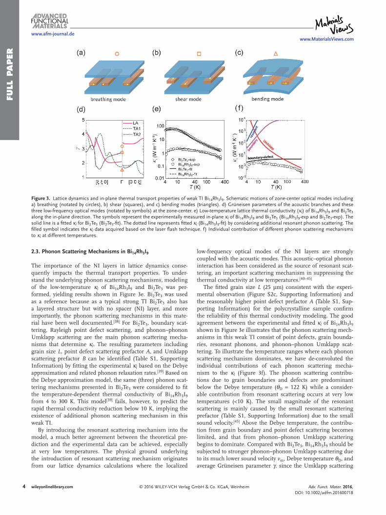
The importance of the NI layers in lattice dynamics conse-quently impacts the thermal transport properties. To under-stand the underlying phonon scattering mechanisms, modeling of the low-temperature κl of Bi14Rh3I9 and Bi2Te3 was per-formed, yielding results shown in Figure 3e. Bi2Te3 was used as a reference because as a typical strong TI Bi2Te3 also has a layered structure but with no spacer (NI) layer, and more importantly, the phonon scattering mechanisms in this mate-rial have been well documented.[38] For Bi2Te3, boundary scat-tering, Rayleigh point defect scattering, and phonon–phonon Umklapp scattering are the main phonon scattering mecha-nisms that determine κl. The resulting parameters including grain size L, point defect scattering prefactor A, and Umklapp scattering prefactor B can be identified (Table S1, Supporting Information) by fitting the experimental κl based on the Debye approximation and related phonon relaxation rates.[39] Based on the Debye approximation model, the same (three) phonon scat-tering mechanisms presented in Bi2Te3 were considered to fit the temperature-dependent thermal conductivity of Bi14Rh3I9 from 4 to 300 K. This model[39] fails, however, to predict the rapid thermal conductivity reduction below 10 K, implying the existence of additional phonon scattering mechanism in this weak TI.
By introducing the resonant scattering mechanism into the model, a much better agreement between the theoretical pre-diction and the experimental data can be achieved, especially at very low temperatures. The physical ground underlying the introduction of resonant scattering mechanism originates from our lattice dynamics calculations where the localized
low-frequency optical modes of the NI layers are strongly coup led with the acoustic modes. This acoustic–optical phonon interaction has been considered as the source of resonant scat-tering, an important scattering mechanism in suppressing the thermal conductivity at low temperatures.[40–45]
The fitted grain size L (25 μm) consistent with the experi-mental observation (Figure S2c, Supporting Information) and the reasonably higher point defect prefactor A (Table S1, Sup-porting Information) for the polycrystalline sample confirm the reliability of this thermal conductivity modeling. The good agreement between the experimental and fitted κl of Bi14Rh3I9 shown in Figure 3e illustrates that the phonon scattering mech-anisms in this weak TI consist of point defects, grain bounda-ries, resonant phonons, and phonon–phonon Umklapp scat-tering. To illustrate the temperature ranges where each phonon scattering mechanism dominates, we have de-convoluted the individual contributions of each phonon scattering mecha-nism to the κl (Figure 3f). The phonon scattering contribu-tions due to grain boundaries and defects are predominant below the Debye temperature (θD = 122 K) while a consider-able contribution from resonant scattering occurs at very low temperatures (<10 K). The small magnitude of the resonant scattering is mainly caused by the small resonant scattering prefactor (Table S1, Supporting Information) due to the small sound velocity.[45] Above the Debye temperature, the contribu-tion from grain boundary and point defect scattering becomes limited, and that from phonon–phonon Umklapp scattering begins to dominate. Compared with Bi2Te3, Bi14Rh3I9 should be subjected to stronger phonon–phonon Umklapp scattering due to its much lower sound velocity vm, Debye temperature θD, and average Grüneisen parameter γ, since the Umklapp scattering
Adv. Funct. Mater. 2016, DOI: 10.1002/adfm.201600718
www.afm-journal.dewww.MaterialsViews.com
Figure 3. Lattice dynamics and in-plane thermal transport properties of weak TI Bi14Rh3I9. Schematic motions of zone-center optical modes including a) breathing (notated by circles), b) shear (squares), and c) bending modes (triangles). d) Grüneisen parameters of the acoustic branches and these three low-frequency optical modes (notated by symbols) at the zone-center. e) Low-temperature lattice thermal conductivity (κl) of Bi14Rh3I9 and Bi2Te3 along the in-plane direction. The symbols represent the experimentally measured in-plane κl of Bi14Rh3I9 and Bi2Te3 (Bi14Rh3I9-exp and Bi2Te3-exp). The solid line is a fitted κl for Bi2Te3 (Bi2Te3-fit). The dotted line represents fitted κl (Bi14Rh3I9-fit) by considering additional resonant phonon scattering. The filled symbol indicates the κl data acquired based on the laser flash technique. f) Individual contribution of different phonon scattering mechanisms to κl at different temperatures.

FULL P
APER
5wileyonlinelibrary.com© 2016 WILEY-VCH Verlag GmbH & Co. KGaA, Weinheim
relaxation time rate τ γθ
ω θ−
− ~ exp3
U1
2
m2
D
2 D
MvT
T, where M is
the average atomic mass and ω is the phonon frequency.[46] Therefore, the existence of NI layers of Bi14Rh3I9, which brings about the low sound velocity and strong lattice anharmonicity, should be responsible for the large difference in the room-tem-perature κl observed in these two TI materials. The robustness of κl against annealing treatment and Pd-doping further sub-stantiates that the point defect scattering in our samples is of less importance at room temperature (Figure S4, Supporting Information) and the observed MTC is essentially caused by the strong phonon–phonon Umklapp scattering.
2.4. Thermoelectric Properties of Bi14Rh3I9
The temperature dependence of TE properties of pristine Bi14Rh3I9, including the electrical resistivity (ρ), Seebeck coef-ficient (α), carrier concentration (n), Hall mobility (μ), and the 300–550 K thermal transport properties and ZT, measured along two different directions, is shown in Figure 4. Large ani-sotropy exists not only in the thermal transport properties, but also in the electrical resistivity and carrier mobility. The strong anisotropic electrical resistivity can be linked to the anisotropic mobility dominated by the quasi-2D electronic structure as reported by Rasche et al.[24] This anisotropic electronic structure is considered as a consequence of the crystal structure of this weak TI since the electron hopping between the QSH layers is weakened by the presence of the NI layers. With increasing the temperature, the electrical resistivity along both the in-plane and cross-plane directions first increases, showing a heavily doped semiconducting behavior, and then decreases around 350 K where the intrinsic excitation becomes significant. Accordingly, at 350 K Bi14Rh3I9 exhibits a maximum Seebeck coefficient close to −200 μV K−1, which is largely determined by the value of the bandgap (about 0.3 eV).[24] In the temperature range of 4–300 K, the pristine Bi14Rh3I9 possesses a less temperature-dependent carrier concentration among 5–7 × 1019 cm−3. The n-type conductance of Bi14Rh3I9 determined by the Hall meas-urements is presumably due to the deficiency of iodine during the sample preparation. A mixed acoustic phonon and ionized impurity scattering contribution can be speculated from the T−1 temperature dependence of the Hall mobility, as shown in Figure 4d. Therefore, the low Hall mobility should be attributed to the stack structure of this weak TI and the dominance of ion-ized impurity scattering.
The electronic contribution (κe) to the total thermal conduc-tivity is very limited for the pristine Bi14Rh3I9. The total thermal conductivity (κ) and κl show a similar temperature dependence, presenting a very slight reduction above the room temperature and followed by an increment above 400 K. The small tem-perature dependence of κl is consistent with the occurrence of MTC, which suggests that the heat-carrying phonons have very small phonon mean free paths approaching their minimum value: on the order of one-phonon wavelength. The increase at higher temperatures should be due to the increased contribu-tion from the bipolar thermal conductivity. Benefitting from the MTC, the pristine Bi14Rh3I9 now shows a TE figure of merit ZT of around 0.3 at 425 K, which is comparable to that of the
undoped binary Bi2Te3 materials (ZT = 0.2–0.3 at 300 K).[47,48] Higher ZT of Bi14Rh3I9 is expected if increased surface state contributions can be incorporated in the future in, for example, nanowires or samples with nano-grains for which the surface-to-volume ratios are significantly higher.[17]
2.5. Lattice Dynamics of Bi2TeI
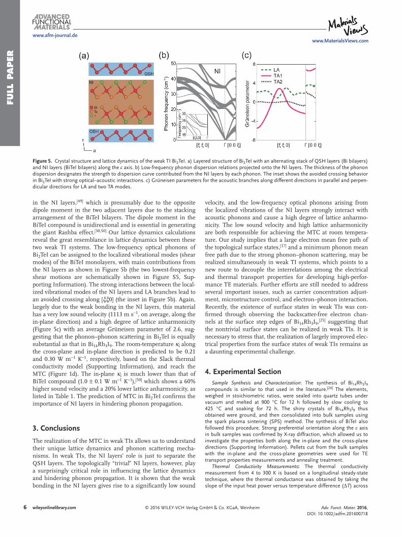
The observed MTC in Bi14Rh3I9 is largely due to the NI layers, which not only decouple the interaction between the QSH layers, but also bring about significant influence on the lattice dynamics, implying that the realization of MTC is highly repro-ducible in those weak TIs which feature a similar stacking struc-ture. Bi2TeI belongs to the Z2 (0; 001) class and has a crystal structure of alternately stacked by QSH layers (Bi bilayers) and NI layers (BiTeI bilayers),[27] as shown in Figure 5a. Weak bonding between the adjacent BiTeI monolayers also exists
Adv. Funct. Mater. 2016, DOI: 10.1002/adfm.201600718
www.afm-journal.dewww.MaterialsViews.com
Figure 4. Temperature dependence of the thermoelectric properties of pristine Bi14Rh3I9 along the in-plane and cross-plane directions, including a) electrical resistivity, b) Seebeck coefficient, c) carrier concentration, and d) Hall mobility. The straight line in (d) indicates a temperature depend-ence of T−1 for the high temperatures (above liquid nitrogen temperature). e) Temperature dependence of the total thermal conductivity, electronic thermal conductivity, and lattice thermal conductivity. The dashed lines represent the in-plane minimum thermal conductivity calculated by the Slack model (upper black line) and Cahill model (lower blue line). f) The figure of merit ZT as a function of temperature.
FULL
PAPER
6 wileyonlinelibrary.com © 2016 WILEY-VCH Verlag GmbH & Co. KGaA, Weinheim
in the NI layers,[49] which is presumably due to the opposite dipole moment in the two adjacent layers due to the stacking arrangement of the BiTeI bilayers. The dipole moment in the BiTeI compound is unidirectional and is essential in generating the giant Rashba effect.[30,50] Our lattice dynamics calculations reveal the great resemblance in lattice dynamics between these two weak TI systems. The low-frequency optical phonons of Bi2TeI can be assigned to the localized vibrational modes (shear modes) of the BiTeI monolayers, with main contributions from the NI layers as shown in Figure 5b (the two lowest-frequency shear motions are schematically shown in Figure S5, Sup-porting Information). The strong interactions between the local-ized vibrational modes of the NI layers and LA branches lead to an avoided crossing along [ξξ0] (the inset in Figure 5b). Again, largely due to the weak bonding in the NI layers, this material has a very low sound velocity (1113 m s−1, on average, along the in-plane direction) and a high degree of lattice anharmonicity (Figure 5c) with an average Grüneisen parameter of 2.6, sug-gesting that the phonon–phonon scattering in Bi2TeI is equally substantial as that in Bi14Rh3I9. The room-temperature κl along the cross-plane and in-plane direction is predicted to be 0.21 and 0.30 W m−1 K−1, respectively, based on the Slack thermal conductivity model (Supporting Information), and reach the MTC (Figure 1d). The in-plane κl is much lower than that of BiTeI compound (1.0 ± 0.1 W m−1 K−1),[50] which shows a 60% higher sound velocity and a 20% lower lattice anharmonicity, as listed in Table 1. The prediction of MTC in Bi2TeI confirms the importance of NI layers in hindering phonon propagation.
3. Conclusions
The realization of the MTC in weak TIs allows us to understand their unique lattice dynamics and phonon scattering mecha-nisms. In weak TIs, the NI layers’ role is just to separate the QSH layers. The topologically “trivial” NI layers, however, play a surprisingly critical role in influencing the lattice dynamics and hindering phonon propagation. It is shown that the weak bonding in the NI layers gives rise to a significantly low sound
velocity, and the low-frequency optical phonons arising from the localized vibrations of the NI layers strongly interact with acoustic phonons and cause a high degree of lattice anharmo-nicity. The low sound velocity and high lattice anharmonicity are both responsible for achieving the MTC at room tempera-ture. Our study implies that a large electron mean free path of the topological surface states,[17] and a minimum phonon mean free path due to the strong phonon–phonon scattering, may be realized simultaneously in weak TI systems, which points to a new route to decouple the interrelations among the electrical and thermal transport properties for developing high-perfor-mance TE materials. Further efforts are still needed to address several important issues, such as carrier concentration adjust-ment, microstructure control, and electron–phonon interaction. Recently, the existence of surface states in weak TIs was con-firmed through observing the backscatter-free electron chan-nels at the surface step edges of Bi14Rh3I9,[25] suggesting that the nontrivial surface states can be realized in weak TIs. It is necessary to stress that, the realization of largely improved elec-trical properties from the surface states of weak TIs remains as a daunting experimental challenge.
4. Experimental SectionSample Synthesis and Characterization: The synthesis of Bi14Rh3I9
compounds is similar to that used in the literature.[24] The elements, weighed in stoichiometric ratios, were sealed into quartz tubes under vacuum and melted at 900 °C for 12 h followed by slow cooling to 425 °C and soaking for 72 h. The shiny crystals of Bi14Rh3I9 thus obtained were ground, and then consolidated into bulk samples using the spark plasma sintering (SPS) method. The synthesis of BiTeI also followed this procedure. Strong preferential orientation along the c axis in bulk samples was confirmed by X-ray diffraction, which allowed us to investigate the properties both along the in-plane and the cross-plane directions (Supporting Information). Pellets cut from the bulk samples with the in-plane and the cross-plane geometries were used for TE transport properties measurements and annealing treatment.
Thermal Conductivity Measurements: The thermal conductivity measurement from 4 to 300 K is based on a longitudinal steady-state technique, where the thermal conductance was obtained by taking the slope of the input heat power versus temperature difference (ΔT) across
Adv. Funct. Mater. 2016, DOI: 10.1002/adfm.201600718
www.afm-journal.dewww.MaterialsViews.com
Figure 5. Crystal structure and lattice dynamics of the weak TI Bi2TeI. a) Layered structure of Bi2TeI with an alternating stack of QSH layers (Bi bilayers) and NI layers (BiTeI bilayers) along the c axis. b) Low-frequency phonon dispersion relations projected onto the NI layers. The thickness of the phonon dispersion designates the strength to dispersion curve contributed from the NI layers by each phonon. The inset shows the avoided crossing behavior in Bi2TeI with strong optical–acoustic interactions. c) Grüneisen parameters for the acoustic branches along different directions in parallel and perpen-dicular directions for LA and two TA modes.
FULL P
APER
7wileyonlinelibrary.com© 2016 WILEY-VCH Verlag GmbH & Co. KGaA, Weinheim
the samples, when sweeping ΔT at a fixed base temperature. Samples (typical dimensions of 4 × 4 × 7 mm3) were directly anchored to the cold copper tip of the cryostat, which served as a heat sink. A strain gauge heater with 350 ohm resistance was used and two copper-constantan thermocouples were used to monitor ΔT. The thermocouples were soldered onto the samples to ensure good thermal contacts. We used long and thin copper and constantan wires (25 μm in diameter) for minimizing the heat flux through the thermocouples. The same thin copper wires were used as current and voltage probes for the heater and for electrical resistivity measurements. A digital camera with a 30× magnification was used to measure the separation between the two thermocouples. In the cryostat that we used for low temperature thermal conductivity measurements, samples are enclosed in a can that can be evacuated by a turbo pumping station to a pressure of less than 10−6 torr. The heat conduction through residue gas is therefore negligible. Radiation losses cannot be eliminated completely, which can be significant above 100 K. Radiation losses from the strain-gauge heater and the sample are minimized by making the heater as small as practically possible and by surrounding the sample with a gold-plated shield thermally grounded to the heat sink. With these precautions, radiation losses can be controlled to minimal values. The magnitude of ΔT was controlled manually to better than 2% of the base temperature. The relative uncertainty of our low temperature thermal conductivity measurement is typically less than ±5%. The absolute uncertainty is limited by the accuracy in determining the geometrical factor Ls/sa (where Ls is the separation between the two thermocouples and sa is the cross-sectional area of the samples) as well as the radiation losses, which can be >±10%. The high-temperature κ from 300 to 550 K was evaluated from the measured thermal diffusion coefficient (D), heat capacity (Cp), and density (ρ0) using κ = DCpρ0. Here D was measured on a Netzsch LFA457 system by using the laser flash technique and Cp was acquired from a DSC404 apparatus. ρ0 was measured by the Archimedes method. The uncertainty in the total κ, measured with the help of the laser flash technique, was estimated to be less than ±10%. When we compare the room temperature thermal conductivity value determined by the low temperature steady-state method with that by the laser flash technique (for high temperatures), there is a 25% discrepancy. This indicates that the steady-state method we used could have up to ±20% radiation losses induced uncertainties at room temperature. The electronic thermal conductivity was estimated based on the Wiedemann–Franz law as used for Bi2Te3,[38] with the Lorenz number L0 being 2.0 × 10⁻⁸ V2 K−2. The lattice thermal conductivity was determined by subtracting the electronic component from the total thermal conductivity. Detailed measurements and results for the electrical transport properties and ZT are given in the Supporting Information.
Lattice Dynamics Calculations: Lattice dynamics for various compounds was investigated with the frozen phonon method,[51] which was implemented in the phonopy package.[52] The compounds studied are the weak TIs Bi14Rh3I9 and Bi2TeI, compounds BiI3 and BiTeI, as well as the QSH monolayer of Bi14Rh3I9 with large spatial distance along the [001] direction. The initial structures and atomic positions are taken from the refs. [24,53]. We constructed a supercell of fully relaxed formula units for each compound or structural unit, and calculated the Hellmann–Feynman forces for the supercell with small displacements (1 pm for each nonequivalent atom). First-principles calculations were performed with the Vienna ab initio simulation package (VASP).[54] Localized density approximation (LDA) functional and projected augmented wave (PAW) methods were used.[55,56] We set the convergence criteria to be 10−5 eV Å−1 for structural relaxation of the unit cell, and 10−8 eV for static calculations of the displaced supercell to ensure the accuracy of phonon results.
Supporting InformationSupporting Information is available from the Wiley Online Library or from the author.
AcknowledgementsP.W. and J.Y. contributed equally to this work. This work was supported by the US Department of Energy under corporate agreement DE-FC26-04NT42278, by GM, and by the National Science Foundation under award number 1235535. W.Z. and Q.Z. are supported by the National Basic Research Program of China (973 program) under project 2013CB632505, and the 111 Project of China (Grant No. B07040). M.S.D is supported by EFRC, #DE-SC0001299. P.W. is supported by the National Natural Science Foundation of China (No. 51502228). W. Zhang would like to acknowledge support by Natural Science Foundation of China under Grant No. 11234012 and No. 51572167, and by Program of Shanghai Subject Chief Scientist (No. 16XD1401100).
Received: February 9, 2016Revised: March 28, 2016
Published online:
[1] M. S. Dresselhaus, G. Chen, M. Y. Tang, R. Yang, H. Lee, D. Wang, Z. Ren, J.-P. Fleurial, P. Gogna, Adv. Mater. 2007, 19, 1043.
[2] J. P. Heremans, V. Jovovic, E. S. Toberer, A. Saramat, K. Kurosaki, A. Charoenphakdee, S. Yamanaka, G. J. Snyder, Science 2008, 321, 554.
[3] G. J. Snyder, E. S. Toberer, Nat. Mater. 2008, 7, 105.[4] Y. Z. Pei, X. Y. Shi, A. LaLonde, H. Wang, L. D. Chen, G. J. Snyder,
Nature 2011, 473, 66.[5] C. J. Vineis, A. Shakouri, A. Majumdar, M. G. Kanatzidis, Adv. Mater.
2010, 22, 3970.[6] J. Yang, H.-L. Yip, A. K.-Y. Jen, Adv. Energy Mater. 2013, 3, 549.[7] D. Kong, Y. Cui, Nat. Chem. 2011, 3, 845.[8] H. J. Zhang, C. X. Liu, X. L. Qi, X. Dai, Z. Fang, S. C. Zhang,
Nat. Phys. 2009, 5, 438.[9] Y. Xia, D. Qian, D. Hsieh, L. Wray, A. Pal, H. Lin, A. Bansil,
D. Grauer, Y. S. Hor, R. J. Cava, M. Z. Hasan, Nat. Phys. 2009, 5, 398.
[10] C. L. Kane, E. J. Mele, Phys. Rev. Lett. 2005, 95, 146802.[11] L. Fu, C. L. Kane, E. J. Mele, Phys. Rev. Lett. 2007, 98, 106803.[12] M. Z. Hasan, C. L. Kane, Rev. Mod. Phys. 2010, 82, 3045.[13] R. Takahashi, S. Murakami, Phys. Rev. B 2010, 81, 161302(R).[14] Z. Fan, J. Zheng, H.-Q. Wang, J.-C. Zheng, Nano Res. Lett. 2012, 7,
570.[15] L. Müchler, F. Casper, B. Yan, S. Chadov, C. Felser, Phys. Status
Solidi RRL 2013, 7, 91.[16] P. Ghaemi, R. S. K. Mong, J. E. Moore, Phys. Rev. Lett. 2010, 105,
166603.[17] Y. Xu, Z. Gan, S.-C. Zhang, Phys. Rev. Lett. 2014, 112, 226801.[18] G. A. Slack, CRC Handbook of Thermoelectrics, CRC, Boca Raton, FL,
USA 1995.[19] G. A. Slack, Solid State Physics (Eds: F. Seitz, D. Turnbull, H. Ehren-
reich), Academic Press, New York 1979.[20] E. C. Skoug, D. T. Morelli, Phys. Rev. Lett. 2011, 107, 235901.[21] C. Chiritescu, D. G. Cahill, N. Nguyen, D. Johnson, A. Bodapati,
P. Keblinski, P. Zschack, Science 2007, 315, 351.[22] L. Fu, C. L. Kane, Phys. Rev. B 2007, 76, 045302.[23] B. Yan, L. Müchler, C. Felser, Phys. Rev. Lett. 2012, 109, 116406.[24] B. Rasche, A. Isaeva, M. Ruck, S. Borisenko, V. Zabolotnyy,
B. Buchner, K. Koepernik, C. Ortix, M. Richter, J. van den Brink, Nat. Mater. 2013, 12, 422.
[25] C. Pauly, B. Rasche, K. Koepernik, M. Liebmann, M. Pratzer, M. Richter, J. Kellner, M. Eschbach, B. Kaufmann, L. Plucinski, C. M. Schneider, M. Ruck, J. van den Brink, M. Morgenstern, Nat. Phys. 2015, 11, 338.
[26] D. G. Cahill, S. K. Watson, R. O. Pohl, Phys. Rev. B 1992, 46, 6131.
Adv. Funct. Mater. 2016, DOI: 10.1002/adfm.201600718
www.afm-journal.dewww.MaterialsViews.com

FULL
PAPER
8 wileyonlinelibrary.com © 2016 WILEY-VCH Verlag GmbH & Co. KGaA, Weinheim Adv. Funct. Mater. 2016, DOI: 10.1002/adfm.201600718
www.afm-journal.dewww.MaterialsViews.com
[27] P. Z. Tang, B. H. Yan, W. D. Cao, S. C. Wu, C. Felser, W. H. Duan, Phys. Rev. B 2014, 89, 041409(R).
[28] C. B. Satterthwaite, R. W. Ure, Phys. Rev. 1957, 108, 1164.[29] R. Venkatasubramanian, E. Siivola, T. Colpitts, B. O’Quinn, Nature
2001, 413, 597.[30] K. Ishizaka, M. S. Bahramy, H. Murakawa, M. Sakano,
T. Shimojima, T. Sonobe, K. Koizumi, S. Shin, H. Miyahara, A. Kimura, K. Miyamoto, T. Okuda, H. Namatame, M. Taniguchi, R. Arita, N. Nagaosa, K. Kobayashi, Y. Murakami, R. Kumai, Y. Kaneko, Y. Onose, Y. Tokura, Nat. Mater. 2011, 10, 521.
[31] B.-L. Huang, M. Kaviany, Phys. Rev. B 2008, 77, 125209.[32] A. Jorio, R. Saito, G. Dresselhaus, M. S. Dresselhaus, Raman
Spectroscopy in Graphene Related Systems, Wiley-VCH, Weinheim, Germany 2011.
[33] J. S. Tse, V. P. Shpakov, V. R. Belosludov, F. Trouw, Y. P. Handa, W. Press, Europhys. Lett. 2001, 54, 354.
[34] J. S. Tse, M. A. White, J. Phys. Chem. 1988, 92, 5006.[35] X. Ling, L. Liang, S. Huang, A. A. Puretzky, D. B. Geohegan,
B. G. Sumpter, J. Kong, V. Meunier, M. S. Dresselhaus, Nano Lett. 2015, 15, 4080.
[36] J. Q. Jenkins, J. A. Rayne, R. W. Ure, Phys. Rev. B 1972, 5, 3171.[37] L. D. Zhao, S. H. Lo, Y. S. Zhang, H. Sun, G. J. Tan, C. Uher,
C. Wolverton, V. P. Dravid, M. G. Kanatzidis, Nature 2014, 508, 373.[38] H. Chi, W. Liu, K. Sun, X. L. Su, G. Y. Wang, P. Lošt’ák, V. Kucek,
C. Drašar, C. Uher, Phys. Rev. B 2013, 88, 045202.[39] J. Callaway, Phys. Rev. 1959, 113, 1046.[40] R. O. Pohl, Phys. Rev. Lett. 1962, 8, 481.
[41] J. L. Cohn, G. S. Nolas, V. Fessatidis, T. H. Metcalf, G. A. Slack, Phys. Rev. Lett. 1999, 82, 779.
[42] Y. Wang, X. Xu, J. Yang, Phys. Rev. Lett. 2009, 102, 175508.[43] J. Yang, W. Zhang, S. Q. Bai, Z. Mei, L. D. Chen, Appl. Phys. Lett.
2007, 90, 192111.[44] W. J. Qiu, L. L. Xi, P. Wei, X. Z. Ke, J. Yang, W. Q. Zhang, Proc. Natl.
Acad. Sci. USA 2014, 111, 15031.[45] L. J. Wu, Q. P. Meng, C. Jooss, J. C. Zheng, H. Inada, D. Su, Q. Li,
Y. M. Zhu, Adv. Funct. Mater. 2013, 23, 5728.[46] G. A. Slack, S. Galginaitis, Phys. Rev. 1964, 133, A253.[47] J. W. G. Bos, H. W. Zandbergen, M.-H. Lee, N. P. Ong, R. J. Cava,
Phys. Rev. B 2007, 75, 195203.[48] M. Scheele, N. Oeschler, K. Meier, A. Kornowski, C. Klinke,
H. Weller, Adv. Funct. Mater. 2009, 19, 3476.[49] S. V. Savilov, V. N. Khrustalev, A. N. Kuznetsov, B. A. Popovkin,
M. Y. Antipin, Russ. Chem. Bull. 2005, 54, 87.[50] L. H. Wu, J. Yang, S. Y. Wang, P. Wei, J. H. Yang, W. Q. Zhang,
L. D. Chen, Phys. Rev. B 2014, 90, 195210.[51] R. Martin, Electronic Structure, Cambridge University Press,
Cambridge, UK 2004.[52] A. Togo, F. Oba, I. Tanaka, Phys. Rev. B 2008, 78, 134106.[53] P. Villars, K. Cenzual, Pearson’s Crystal Data: Crystal Structure
Database for Inorganic Compounds, ASM International, Materials Park, Ohio, USA 2011.
[54] G. Kresse, J. Furthmüller, Phys. Rev. B 1996, 54, 11169.[55] G. Kresse, J. Joubert, Phys. Rev. B 1999, 59, 1758.[56] P. E. Blöchl, Phys. Rev. B 1994, 50, 17953.