Miniaturization of Chip-Scale Photonic...
146
UNIVERSITY OF CALIFORNIA, SAN DIEGO Miniaturization of Chip-Scale Photonic Circuits A dissertation submitted in partial satisfaction of the requirements for the degree Doctor of Philosophy in Electrical Engineering (Photonics) by Steve Zamek Committee in charge: Professor Yeshaiahu Fainman, Chair Professor Andrea R. Tao Professor Bill Lin Professor Vitaliy Lomakin Professor Ramamohan Paturi 2011
Transcript of Miniaturization of Chip-Scale Photonic...

UNIVERSITY OF CALIFORNIA, SAN DIEGO
Miniaturization of Chip-Scale Photonic Circuits
A dissertation submitted in partial satisfaction of the requirements for the degree
Doctor of Philosophy
in
Electrical Engineering (Photonics)
by
Steve Zamek
Committee in charge:
Professor Yeshaiahu Fainman, Chair
Professor Andrea R. Tao
Professor Bill Lin
Professor Vitaliy Lomakin
Professor Ramamohan Paturi
2011

Copyright
Steve Zamek, 2011
All rights reserved.

- iii -
The Dissertation of Steve Zamek is approved, and it is acceptable in quality and form for
publication on microfilm and electronically:
Chair
University of California, San Diego
2011

- iv -
Dedication
To my advisor: Thank you for walking me hand in hand through both professional and
personal difficulties during the years of my studies at UCSD.
To my parents: If it was not your stimulation and support I would have never gone this
far.
To my wife: Thank you for your love and support. Thanks for giving me the reason
to succeed.
To my friends: Without you my PhD would have been a tedious dull routine. Thank
you for all your support and friendship.

- v -
Table of Contents
Dedication .....................................................................................................................iv Table of Contents ..........................................................................................................v List of Figures ............................................................................................................. vii Abbreviations ...............................................................................................................ix Acknowledgements ......................................................................................................x Vita .................................................................................................................................xi Publications..................................................................................................................xii Abstract of the Dissertation ..................................................................................... xiv I. Introduction.............................................................................................................1
1. Historical Outlook. .......................................................................................1 2. Integrated Photonic Circuits. ......................................................................5
2.1. Life Sciences.........................................................................................6 2.2. Information Technologies..................................................................9
3. Chip-Scale Photonics..................................................................................12 3.1. Rationale.............................................................................................13 3.2. Literature Survey. .............................................................................13
4. Overview of the Thesis. .............................................................................16 II. Folded DBRs..........................................................................................................18
1. Introduction.................................................................................................18 2. Chip-scale Bragg gratings..........................................................................18 3. Manufacturability of DBRs........................................................................20
3.1. Fabrication Process. ..........................................................................21 3.2. Effects of Stitching Errors. ...............................................................24 3.3. Discussion. .........................................................................................28
4. Curved Waveguide Bragg Grating. .........................................................30 4.1. Model..................................................................................................31 4.2. Design.................................................................................................36 4.3. Experiment.........................................................................................38
5. Other Techniques for Folding...................................................................41 6. Other Applications. ....................................................................................44 7. Folding of 4-port devices. ..........................................................................44
III. Integrated Metallic Mirrors.................................................................................47 1. 3D Configuration. .......................................................................................47
1.1. Introduction .......................................................................................47 1.2. Description of the Device.................................................................49 1.3. Analytical Model...............................................................................51 1.4. Design.................................................................................................57 1.5. Fabrication .........................................................................................61

- vi -
1.6. Experiment.........................................................................................62 1.7. Discussion. .........................................................................................65 1.8. Improving the Q-factor. ...................................................................67 1.9. Summary............................................................................................68
2. 2D Configuration. .......................................................................................69 2.1. Introduction. ......................................................................................69 2.2. Device Description............................................................................70 2.3. Design.................................................................................................74 2.4. Fabrication. ........................................................................................75 2.5. Experiment.........................................................................................76 2.6. Application to Biochemical Sensing...............................................80 2.7. Summary. ...........................................................................................83
3. Metallic Mirrors - Discussion....................................................................84 IV. Future research directions...................................................................................85
1. Folded Waveguide Bragg Gratings..........................................................85 2. Graphical Methods for Solving Complex Structures.............................85 3. High-Q Resonators with Metallic Mirrors ..............................................86 4. Transformer Based on Through-Coupled Resonator. ...........................88 5. Group Delay Dispersion. ...........................................................................88
V. Summary of the Thesis ........................................................................................89 References ....................................................................................................................90 Appendix A Scattering and Transmission Matrices ..............................................99 Appendix B Waveguide Bending Losses..............................................................102 Appendix C Analysis of a Waveguide Coupled Resonator ...............................107 Appendix D Metallic Mirrors: Fabrication Recipe ...............................................109 Appendix E Lift-off: Fabrication Imperfections...................................................111 Appendix F Directional Coupling .........................................................................112 Appendix G Coupling Coefficient and Supermodes...........................................115 Appendix H Distributed Bragg reflector (DBR). ..................................................117 Appendix I Label-Free Biochemical Sensing.......................................................120 Appendix J Channel Add-Drop Multiplexers.....................................................124 Appendix K Optofluidic Switch .............................................................................126 Appendix L Affinity Sensors – Surface Coverage. ..............................................130
- vii -
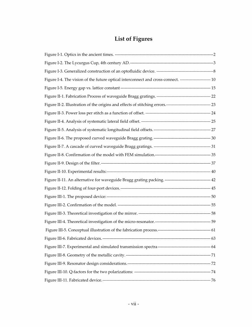
List of Figures
Figure I-1. Optics in the ancient times. -----------------------------------------------------------------------2
Figure I-2. The Lycurgus Cup, 4th century AD.------------------------------------------------------------3
Figure I-3. Generalized construction of an optofluidic device. -----------------------------------------8
Figure I-4. The vision of the future optical interconnect and cross-connect. ---------------------- 10
Figure I-5. Energy gap vs. lattice constant ----------------------------------------------------------------- 15
Figure II-1. Fabrication Process of waveguide Bragg gratings. --------------------------------------- 22
Figure II-2. Illustration of the origins and effects of stitching errors.-------------------------------- 23
Figure II-3. Power loss per stitch as a function of offset. ----------------------------------------------- 24
Figure II-4. Analysis of systematic lateral field offset. -------------------------------------------------- 25
Figure II-5. Analysis of systematic longitudinal field offsets. ----------------------------------------- 27
Figure II-6. The proposed curved waveguide Bragg grating. ----------------------------------------- 30
Figure II-7. A cascade of curved waveguide Bragg gratings. ----------------------------------------- 31
Figure II-8. Confirmation of the model with FEM simulation.---------------------------------------- 35
Figure II-9. Design of the filter. ------------------------------------------------------------------------------- 37
Figure II-10. Experimental results:--------------------------------------------------------------------------- 40
Figure II-11. An alternative for waveguide Bragg grating packing. --------------------------------- 42
Figure II-12. Folding of four-port devices. ----------------------------------------------------------------- 45
Figure III-1. The proposed device:--------------------------------------------------------------------------- 50
Figure III-2. Confirmation of the model. ------------------------------------------------------------------- 55
Figure III-3. Theoretical investigation of the mirror. ---------------------------------------------------- 58
Figure III-4. Theoretical investigation of the micro-resonator.---------------------------------------- 59
Figure III-5. Conceptual illustration of the fabrication process.-------------------------------------- 61
Figure III-6. Fabricated devices. ------------------------------------------------------------------------------ 63
Figure III-7. Experimental and simulated transmission spectra -------------------------------------- 64
Figure III-8. Geometry of the metallic cavity. ------------------------------------------------------------- 71
Figure III-9. Resonator design considerations.------------------------------------------------------------ 72
Figure III-10. Q-factors for the two polarizations: ------------------------------------------------------- 74
Figure III-11. Fabricated device.------------------------------------------------------------------------------ 76

- viii -
Figure III-12. Experimental setup. --------------------------------------------------------------------------- 78
Figure III-13. Experimental results.-------------------------------------------------------------------------- 79
Figure III-14. Concept of high-throughput label-free biochemical sensing. ----------------------- 82

- ix -
Abbreviations
2D two-dimensional 3D three dimensional AFM atomic force microscope/microscopy CMOS complementary metal oxide semiconductor CMT coupled mode theory CPU central processing unit DBR distributed Bragg grating DFB distributed feedback EBL electron beam lithography FDTD finite difference time domain FEM finite element method FSR free spectral range FTTH fiber to the home FWHM full width at half-maximum GVD group velocity dispersion HSQ Hydrogen SilsesQuioxane IC integrated circuits ICP inductively coupled plasma ITRS international technology roadmap for semiconductors LAN local area network LOC lab-on-a-chip MAN metropolitan area networks MIBK Methyl isobutyl ketone NIR near infra-red OADM optical add-drop multiplexer OCT optical coherence tomography OEIC optoelectronic integrated circuits PECVD plasma enhanced chemical vapor deposition PhC photonic crystal PIC photonic integrated circuits PLC planar lightwave circuits PMMA polymethyl methacrylate POC point-of-care RIE reactive ion etching SEM scanning electron microscopy SOI silicon-on-insulator TE transverse electric TM transverse magnetic TMAH Tetramethylammonium Hydroxide UV ultra-violet WAN wide area network WDM wavelength division multiplexing

- x -
Acknowledgements
The text of Chapter Two, in part or in full, is a reprint of the material as it appears in
S. Zamek, D.T.H. Tan, M. Khajavikhan, M. Ayache, M.P. Nezhad, and Y. Fainman,
“Compact chip-scale filter based on curved waveguide Bragg gratings”, Opt. Lett.,
2010, 35, 3477-3479,
The dissertation author was the primary researcher and author. The co-authors listed in
this publication directed and supervised the research which forms the basis for this
chapter.
The text of Chapter Three, in part or in full, is a reprint of the material as it appears in
S. Zamek, L. Feng, M. Khajavikhan, D.T.H. Tan, M. Ayache, Y. Fainman, “Micro-
Resonator with Metallic Mirrors Coupled to a Bus Waveguide“, Optics Express 19
(3), 2011,
and
S. Zamek, A. Mizrahi, L. Feng, A. Simic, Y. Fainman, “On-chip waveguide
resonator with metallic mirrors”, Opt Lett, 2010, 35, 598-600.
The dissertation author was the primary researcher and author. The co-authors listed in
this publication directed and supervised the research which forms the basis for this
chapter.
- xi -
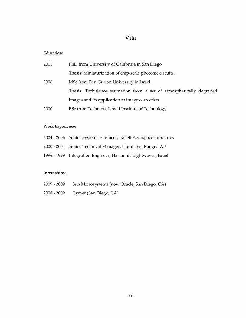
Vita
Education:
2011 PhD from University of California in San Diego
Thesis: Miniaturization of chip-scale photonic circuits.
2006 MSc from Ben Gurion University in Israel
Thesis: Turbulence estimation from a set of atmospherically degraded
images and its application to image correction.
2000 BSc from Technion, Israeli Institute of Technology
Work Experience:
2004 - 2006 Senior Systems Engineer, Israeli Aerospace Industries
2000 - 2004 Senior Technical Manager, Flight Test Range, IAF
1996 - 1999 Integration Engineer, Harmonic Lightwaves, Israel
Internships:
2009 - 2009 Sun Microsystems (now Oracle, San Diego, CA)
2008 - 2009 Cymer (San Diego, CA)
- xii -
Publications
Peer-Reviewed Journal Publications
1. S. Zamek, L. Feng, M. Khajavikhan, D.T.H. Tan, M. Ayache, Y. Fainman, “Micro-Resonator with Metallic Mirrors Coupled to a Bus Waveguide“, Optics Express 19 (2011).
2. S. Zamek, A. Mizrahi, L. Feng, A. Simic, Y. Fainman, “On-chip waveguide resonator with metallic mirrors”, Optics Letters 35, 598-600 (2010).
3. S. Zamek, D.T.H. Tan, M. Khajavikhan, M. Ayache, M.P. Nezhad, and Y. Fainman, “Compact chip-scale filter based on curved waveguide Bragg gratings”, Optics Letters 35, 3477-3479 (2010).
4. S. Zamek and Y. Yitzhaky, "Turbulence strength estimation from an arbitrary set of atmospherically degraded images," J. Opt. Soc. Am. A 23, 3106-3113 (2006).
5. A. Groisman, S. Zamek, K. Campbell, L. Pang, U. Levy, Y. Fainman, “Optofluidic 1x4 switch”, Optics Express 16, 13499-13508 (2008).
6. D. T. H. Tan, K. Ikeda, S. Zamek, A. Mizrahi, M.P. Nezhad, A.V. Krishnamoorthy, K. Raj, J.E. Cunningham, X. Zheng, I. Shubin, Y. Luo and Y. Fainman, “Wide bandwidth, low loss 1 by 4 wavelength division multiplexer on silicon for optical interconnects” , Opt. Express 19, 2401-2409 (2011).
7. M. Ayache, M. P. Nezhad, S. Zamek, M. Abashin, and Y. Fainman, “Near-Field Measurement of Amplitude and Phase in Silicon Waveguides with Liquid Cladding”, submitted to Optics Letters.
8. R. E. Saperstein, N. Alic, S. Zamek, K. Ikeda, B. Slutsky, and Y. Fainman, "Processing advantages of linear chirped fiber Bragg gratings in the time domain realization of optical frequency-domain reflectometry," Optics Express 15, 15464-15479 (2007).
Book Chapters
1. S. Zamek, B. Slutsky, L. Pang, U. Levy, Y. Fainman, “Optofluidic Switches and Sensors”, in Handbook of Optofluidics, CRC 2010.
2. S. Zamek and Y. Fainman, “Adaptive Optofluidic Devices”, in Optofluidics:
Fundamentals, Devices, and Applications, McGraw Hill 2010.

- xiii -
Peer-Reviewed Conference Proceedings
1 S. Zamek, D.T.H. Tan, M. Khajavikhan, M.P. Nezhad, and Y. Fainman, “Curved Waveguide Bragg Gratings on a Chip”, FIO 2010.
2 S. Zamek, A. Mizrahi, L. Feng, A. Simic, Y. Fainman, Y. “Planar dielectric cavity for biochemical sensing”, 22nd Annuall Meeting of the IEEE Lasers and Electro-Optics Society, LEO 2009, 262-3.
3 S. Zamek, L. Campbell, L. Pang, A. Groisman, Y. Fainman, “Optofluidic 1x4 switch”, CLEO 2008.
4 S. Zamek and Y. Yitzhaky, “Turbulence strength estimation and super-resolution from an arbitrary set of atmospherically degraded images,” in Atmospheric Optical Modeling, Measurement, and Simulation II, part of SPIE’s symposium in San Diego, CA., August 2006.
5 D. T. H. Tan, K. Ikeda, S. Zamek, A. Mizrahi, M.P. Nezhad, A.V. Krishnamoorthy, K. Raj, J.E. Cunningham, X. Zheng, Y. Luo and Y. Fainman, “Wide Bandwidth, Low Loss 1 by 4 Wavelength Division Multiplexer on Silicon“, Photonics Global, Singapore, Dec 2010.
6 J. E. Cunningham, I. Shubin, S. Zamek, D. Popivitch, A. Krishnamoorthy, J. Mitchell, “Ferro-Electrically Enhanced Proximity Communications: Microfabrication and Characterization”, IMAPS 2010.
7 D. T. H. Tan, K. Ikeda, S. Zamek, A. Mizrahi, M. P. Nezhad and Y. Fainman, “Wavelength Selective Coupler on Silicon for Applications in Wavelength Division Multiplexing”, SUM 2010 IEEE, Optical Networks and Datacenters.
8 M. P. Nezhad, S. Zamek, L. Pang, Y. Fainman, “Fabrication approaches for metallo-dielectric plasmonic waveguides”, SPIE: Advanced Fabrication Technologies For Micro/Nano Optics And Photonics, 2008, Vol. 6883, pp. S8830-S8830.
9 M. P. Nezhad, S. Zamek, L. Pang, and Y. Fainman, "Fabrication techniques for long range surface plasmon waveguides," Annual Meeting Conference Proceedings. IEEE, LEOS 2007, pp. 604-605.
10 R. E. Saperstein, S. Zamek, K. Ikeda, B. Slutsky, N. Alic, and Y. Fainman, "Chirped Pulse Optical Ranging," in FIO, OSA 2007, FMH3.

- xiv -
Abstract of the Dissertation
Miniaturization of Chip-Scale Photonic Circuits
by
Steve Zamek
Doctor of Philosophy
in
Electrical Engineering (Photonics)
University of California, San Diego, 2011
Professor Yeshaiahu Fainman, Chair
Chip-scale photonic circuits promise to alleviate some fundamental physical
barriers encountered in many areas of the life sciences and information technologies.
This thesis investigates routes to miniaturization of chip-scale optical devices. Two new
techniques and devices based thereon are introduced for the first time. One technique
makes use of integrated metallic mirrors to construct reflectors which are by an order of
magnitude smaller than their counterparts. Another technique is based on folding of
chip-scale devices to fit long structures into small area on a chip. Although both
techniques are demonstrated on some specific examples, the developed toolkit is

- xv -
applicable to a wide range of chip-scale devices including modulators, filters, channel
add-drop multiplexers, detectors, and others.
The major part of this Thesis focuses on miniaturization of waveguide reflectors
and the devices based thereon. Fitting long waveguide Bragg gratings into a small area
on a chip is demonstrated based on curved waveguide Bragg gratings; theory and
analytical model of such structures is developed. In the second part of the Thesis,
integrated metallic mirrors are proposed as reflectors with properties complementary to
Bragg gratings - low polarization sensitivity, high reflectivity for different transverse
modes, and good manufacturability. The feasibility of the proposed ideas is tested in
both simulations and experiments. The demonstrated devices including biochemical
sensors, micro-resonators, and inline filters are promising for applications in the life
sciences and information technologies.

- 1 -
I. Introduction
1. Historical Outlook.
Light has always intrigued the humankind and inspired our imagination.
Mythological, religious, and supernatural powers were attributed to it by our
predecessors. The ancient Egyptians, Hindus, Romans, and Greeks worshipped light
and its powers. It got a place of honor in the book of Genesis. Heliographing, or optical
signaling by reflecting the sun light, was widely employed by Alexander the Great, the
King of Macedonia, and by his Roman successors several hundreds of years later. In the
years 214-212 BC Archimedes constructed a huge mirror which was used by the Romans
in the siege of Syracuse to deflect the sun light and set fire to the sails of enemy’s vessels
[Kingman 1919, Partington 1835]. The legendary act was captured in several paintings,
with an example shown in Figure I-1(a). Several years before the Common Era,
heliography became so efficient, that entire text messages could be transmitted. Tiberius,
the successor of Augustus and the ruler of the Roman Empire, managed to run his
affairs from the Isle of Capri, 160 miles away from Rome by transmitting encoded
messages using such a technique [Kingman 1919] (see the map on Figure I-1(b)).
Ironically, similar schemes of optical signaling were still in use in 1960s by the British
and Australian armies. Today, a single optical fiber allows bandwidths of over 1 TB/s be
transmitted over distances of hundreds and thousands of kilometers.

2
Figure I-1. Optics in the ancient times. (a) The wall painting of Archimedes’ military
feat from the Stanzino delle Matematiche in the Galleria degli Uffizi, Florence, Italy,
painted by Giulio Parigi (1571-1635) in the years 1599-1600. (b) Map showing stations
of wireless optical signaling in the Roman Empire. The map shows the Isle of Capri
and Rome with a distance of 160 miles between them.
Besides its extensive use in communications and warfare, optical materials were
used by the ancient masters of Arts to create objects of extraordinary appearance. As
early as 4th century AD, there already existed the expertise in making use of metal nano-
Rome
Isle of Capri
100 miles
(a)
(b)

3
particles dispersed in glass to create materials with compelling appearance, as the one
shown in Figure I-2. The color of the cup shown in the figure would change depending
on the angle of illumination. Similar techniques were used much later by medieval
artists in church icons to give them dazzling appearance varying during the day. It took
Figure I-2. The Lycurgus Cup, 4th century AD. Kept in the British Museum. The cup
illuminated from the front (a) and from the back (b).
the humanity over two thousand years to be able to understand the phenomenon well
known to the ancient world, and provide a scientific explanation to it [Harden 1959,
Brongersma 2007, Zehetbauer 2009, Stockman 2010].
In the 16th century an optical microscope was invented, with the outcomes
difficult to comprehend. Followed by three hundred years of improvements of design
and illumination techniques, it gave a glimpse into the structure of materials and lead to
the discovery of live cells. Contrast illumination techniques introduced in the late 19th
(a) (b)

4
and early 20th century allowed imaging of transparent samples – capability that proved
crucial in biology and medicine.
By this time Scottish physicist James Clerk Maxwell already laid out the theory of
Electromagnetism, and the last of the great Victorian polymaths, Lord Rayleigh, was
working on the wave nature of optics and phenomena of diffraction. Charles Fabry and
Henri Buisson explained the interference fringes observed with coherent light; Scottish
physicist, John Kerr, made his discoveries of double refraction in dielectrics subjected to
an electrostatic field; Indian scientist, C. V. Raman showed inelastic scattering of
photons by atoms and molecules; American physicist Albert Abraham Michelson
conducted successful experiments establishing the speed of light, and many more
discoveries followed right after.
The endeavors of the 20th century in the field of optics were no less remarkable.
The photoelectric effect, discovered in the end of 19th century, was explained by Albert
Einstein in 1905 in a work that opened a new era in physics. Light was now described as
a wave, having energy quanta (photons), related to its wavelength (color). This was
followed by the works of Einstein, Plank, de-Broglie, Schrödinger, Heisenberg, and
many others. The wave-particle behavior of light makes possible generation,
manipulation, and detection of light as we know it today. The fundamental scientific
work was followed by demonstration of the first functioning laser in the 1960 [Mainman
1960], followed shortly after by the first demonstration of semiconductor laser diode in
1962 [Dumke 1962]. The invention of laser was recognized as one of the ground-

5
breaking scientific achievements of the 20th century. Demonstration of room temperature
operation of semiconductor lasers with the advent of low loss optical fiber in the 1970s
opened a new era of lightwave technology. Commercialization of erbium doped
amplifiers, fiber Bragg gratings, and wavelength division multiplexing were crucial
milestones that allowed the capacity of commercial fiber system to exceed 1.6 TB/s by
2001 [Agrawal 2004]. Excellent overviews of the discoveries in the field of optics can be
found in textbooks (see Historical Introduction in [Born 1999] and the references therein).
At the same time optical technologies were taking giant leaps in the areas of the
Life Sciences. The plethora of physical phenomena in light-matter interactions made
optical techniques extremely efficient as research tools, diagnostics, therapeutics, and
surgery. The commercialized spectroscopy, chromatography, and microscopy
instruments and sensors became now being extensively used. New disciplines emerged
from the above mentioned discoveries and applications – biophotonics and optofluidics
[vo-Dinh 2003, Pavesi 2008, Fainman 2010, Hawkins 2010].
2. Integrated Photonic Circuits.
The end of 20th and the beginning of 21st centuries saw a new trend in optics.
Both, the life sciences and information technologies started moving in the direction of
integrated chip-scale optics, dictated by costs and application requirements. The major
idea behind chip-scale optics is to integrate multiple optical devices in a single chip, that
could be created with the existing high-volume manufacturing tools, such as those
employed by the microelectronic industry. High-volume low-cost manufacturability of a

6
multitude of optical functions is what can make optics a transformational discipline in
the 21st century and beyond. Displacing other technologies and providing new
functionalities at a cost of a dime is the major promise of chip-scale optics. The following
sections of the introduction discuss the application areas of chip-scale optics, application
requirements, and the rationale of chip-scale integration.
Strong impacts of chip-scale photonic circuits are anticipated in the areas of the
life sciences and information technologies. While the former historically employed free-
space optics, the latter exploited fiber optic technology. Both free-space and fiber-based
optical devices are based on the same fundamental principles and utilize similar
physical effects. To facilitate understanding of application areas and their requirements
we provide below a more detailed discussion of the two.
2.1. Life Sciences.
Optics played crucial role in the life sciences on all scales – from the discovery of
distant galaxies, to the studies of human genome and structure of micro-organisms.
Most of the devices used in those application areas are based on free-space optics,
consisting of lenses, mirrors, beam splitters, polarizers, and others. These devices were
applied to material processing, biochemical detection, imaging, and manipulation of
objects on the micro-scale. In biochemistry, for instance, optics is used for genome
sequencing, drug development, biomarkers discovery, environmental monitoring, and
many others [vo-Dinh 2003]. Commercial products that have been introduced for these
applications are large bench-top instruments, both bulky and expensive.

7
Numerous effects such as Raman and Doppler scattering, refraction, diffusion,
and absorption, non-linear effects, chromatic dispersion, fluorescence, FRET, and others
provide extensive data about the matter. Therefore optics is broadly used in the life
science applications for detection, imaging, diagnostics, treatment, and medicine. In
genomics and proteomics biochips and microarrays have already revealed how tens of
thousands of genes and proteins work together in interconnected networks to
orchestrate the chemistry of life [Vo-Dinh]. Lifetime imaging, microscopy, near-field
detection, optical coherence tomography, interferometry, Doppler imaging, light
scattering, and thermal imaging are all examples of photonic detection and imaging
techniques.
Near field imaging and two photon microscopy are two techniques used in
biology to achieve resolutions beyond the diffraction limit of light. Optical coherence
tomography (OCT), speckle correlometry, laser Doppler perfusion monitoring, atomic
spectroscopy are widely used to look deep into tissues gathering information about both
its structure and dynamics. Fluorescent techniques are used for flow cytometry,
biochemical assays, affinity studies, DNA sequencing, and other applications. Optical
trapping and laser welding are used for materials manipulation and processing on the
micro-scales.
Numerous application areas urge for miniaturization of the existing bench-top
instruments into hand-held devices that can be deployed to the field. An example of
such application is point-of-care (POC) diagnostics, which can potentially benefit the

8
humanity on a global scale. Technology known as lab-on-a-chip, has tremendously
expanded and matured but is being continuously investigated by many institutions
across the globe. Lab-on-a-chip journal was launched in 2001 by the Royal Society of
Chemistry, with the purpose of publishing an entire scope of “microfluidic and nanofluidic
technologies for chemistry, physics, biology, and bioengineering”. Even though such
technology succeeded to integrate chemical functions such as sample extraction,
purification, and amplification, it is yet to demonstrate integration of optics and
electronics into a microfluidic platform. This research direction, known as optofluidics,
became an engineering discipline in its own right.
Optofluidics refers to a class of adaptive optical circuits that integrate optical and
fluidic devices. The introduction of liquids in the optical structure enables flexible fine-
tuning and even reconfiguration of circuits such that
Figure I-3. Construction of an optofluidic device. Following the vision of optofluidic,
device consists of three layers: (A) microfluidic controls with micro-valves and
pumps incorporated into this layer; (B) flow channels; (C) the optical structure with
photonic crystals, sensors, sources, and waveguides. Reprinted from [Psaltis 2006].

9
they may perform tasks optimally in a changing environment. A schematic diagram that
summarizes the suggested approach is shown in Figure I-3, where a nano-structured
optical substrate is integrated with a microfluidic structure that performs functions such
as reconfiguration of functionality, adaptation of properties, distribution of chemicals to
be analyzed, and temperature stabilization. Optofluidic devices employ an entire range
of optical components to generate, detect, and manipulate light. Future applications
require techniques for miniaturization and integration of optical chip-scale components
in microfluidic platforms.
2.2. Information Technologies.
The 20th century has seen the latest echoes of the industrial revolution followed by
the information revolution. The social, economic, and technological drives were so
strong, as to establish new scientific disciplines, such as Cybernetics and Information
Theory. The information hunger put under way globe spanning projects, such as the
foundation of the Internet in the late 1960s. In the 1980s optical fiber replaced coaxial
cables, dramatically increasing the bandwidth and reducing the delay time. Optical fiber
got later introduced into wide area networks (WANs), then to metropolitan and local
area networks (MANs and LANs), and has been moving towards the consumer ever
since. In the 1990s wavelength division multiplexing (WDM) was introduced to allow
transmission of multiple optical carriers over a single fiber. That allowed
communication bandwidths in excess of 1 TB/s over a single fiber.

10
Today any powerful computer comes equipped with an optical interface, and
optical components are found in any computer peripherals such as mouse, display, laser
printer, CD-ROM, and others. So how much further can photonics penetrate into all
those information technologies?
Optical communication links between different boards and between different
components on a single board have already been demonstrated [Intel 2010, Assefa 2010].
Experts argue that in the future photonic links will replace the metallic interconnect
used today in the integrated circuits (IC).
Figure I-4. The vision of the future optical interconnect and cross-connect. (a) Cross
section of Intel’s interconnect stack, metallization layers M1-8, employing 32 nm gate
size technology. Reprinted from Real World Technologies online. (b) On-chip optical
network that replaces the metallic interconnect. (c) Block diagram of an optical link
connecting two logic blocks.
(a) (b)
(c)

11
Currently metallic interconnect is used to relay information between different
transistors and IC blocks by driving a current through copper wires, with an example
shown in Figure I-4(a). The shortcomings of the current interconnect technology are
resistive heating, electromagnetic interference between those wires, and time delays due
to the inherent RC time constant. Reliability of metallic interconnect is compromised by
electromigration, stress-voiding, adhesion failures, corrosion, and interdiffusion
[Murarka 1993, Davis 2003, Goel 2007]. Being one of the major bottlenecks of the current
microelectronics industry [Davis 2003], these issues are expected to aggravate as the
number and density of transistors continue scaling according to Moore’s law.
Many of those issues are potentially resolved by photonic links integrated onto the
silicon die [ITRS roadmap]. The two driving forces behind what is called silicon
photonics are (1) the requirements for smart optical networks, greater bandwidths, and
lower cost are pushing the integration of electronics into photonics and (2) the
interconnect bottleneck for CMOS circuits operating above 10 GHz is pushing the
integration of photonics into electronics for timing and possibly signal channels [Pavesi
2004].
The concept of optical interconnect is shown in Figure I-4(b), where an on-chip
optical network is used to relay signals between different IC blocks within the same chip.
The same network interfaces between the chip and other devices such as memory, CPU,
cache, etc. Block diagram of the physical layer is shown in Figure I-4(c). Electronic

12
signals are modulated and multiplexed using wavelength division multiplexing (WDM).
The data is delivered by the network to the desired destination. At the destination,
photo-receivers convert the optical signal back to the electronic domain. The signal is
further conditioned to be readily used by the corresponding logic block.
However the contribution of photonics to the information technologies does not
stop here. Possibility of high volume manufacturing will make photonic components a
commodity. In such paradigm any personal computer, for instance, will become a
member in an optical network. Therefore more bandwidth will be aggregated close to
the consumer, allowing personal high-power computing, richer information content,
and more efficient bandwidth utilization.
3. Chip-Scale Photonics.
Elements of Optics and Photonics are encountered today in the most unexpected
areas of life. Optical data storage devices became a commodity, flat panel displays are
found in most homes across the developed countries of the world, hand-held devices
equipped with cameras continue storming the markets, and fiber-to-the-home (FTTH)
projects are on their way to provide users with new services and ever growing
information content. These achievements were made possible through miniaturization
of optical components and their integration with micro-electronics. Despite this
tremendous progress, further integration of devices into chip-scale photonic circuits is
on its way. Such photonic circuits may revolutionize our lives just as electronics did
during the past decades. The paradigm of photonic circuits is already within reach, with

13
many chip-scale devices demonstrated by both industry and academia. The missing
parts of the chip-scale photonic puzzle are the manufacturability, the validation
capabilities, and the cost effective integration of photonic elements into complex
optoelectronic circuits.
3.1. Rationale.
Integration of photonic elements into complex chip-scale photonic circuits offers
several advantages over the conventional free-space and fiber-optic circuits. First,
possibility of fabrication of chip-scale devices with standard tools used in the IC
manufacturing process will significantly reduce the costs and allow high-volume
manufacturing. Second, it will result in more compact light-weight devices. Such devices
can create new markets that have so far been out of reach for optical technologies.
Furthermore, printed chip-scale optical components do not require alignment, as it is an
inherent feature of the existing lithographic process. Therefore chip-scale devices can
both have lower costs and exhibit higher performance than their free-space or fiber-optic
counterparts.
3.2. Literature Survey.
The extensive research on chip-scale photonic devices, numerous industrial efforts,
and very broad application areas make it impossible to extensively cover the topic of
chip-scale photonic circuits. Excellent reviews and summaries can be found in numerous
textbooks [Martelluci 1981, Nishihara 1989, Tamir 1990, Pollock 2003, Hunsperger 1982,
Coldren 1995, Ebeling 1993, Agrawal 2004, Chang 2009]. In these textbooks different
14
names are interchangeably used for chip-scale photonic devices, with the three most
common ones: photonic integrated circuits (PIC), planar lightwave circuits (PLC), and
opto-electronic integrated circuits (OEIC). These are used to describe different material
platforms and various schemes of integration.
Large variety of material platforms used for implementation of PIC is dictated by
the material properties, device functionality, application requirements, and the
fabrication technology to be used. Optical sources, detectors, and non-linear devices
commonly require semiconductors with the proper band-gap to provide the required
wavelength. Figure I-5 shows the variety of materials with their corresponding band
gaps. Chapter 1 in [Lifante 2002] provides an interesting comparison of material
platforms with respect to the fabrication technologies and materials’ optical properties.
Reviews of devices integrated in InP and GaAs platforms can be found in Chapters 1
and 10 in [Marsh 1990] and Part 4 of [Boyd 1991]. Silicon-on-insulator (SOI) platform is
becoming more popular today [Pollock 2003, Pavesi 2004] due to the lower cost, better
developed fabrication, and availability of silicon with low levels of impurities. The
limiting factors of silicon for optical devices are indirect bandgap, low electron mobility,
and relatively high two-photon absorption.

15
Figure I-5. Energy gap vs. lattice constant for some common elementary and binary
semiconductors. Reprinted from [Sze 2007], p. 57.
From the discussion above it becomes clear that photonic circuits must employ
several different materials to leverage the strengths and functionalities of each.
Therefore integration of several materials is crucial. The early stages of research on
hybrid optical circuits were summarized in [Nishihara 1989]. It covered the first
functional devices employing electro-optic, acoustooptic, magnetooptic, thermooptic,
and nonlinear materials: polymers, glass, chalcogenide, LiNbO3, and SOI. Already in the
1980s, systems integration became an acute challenge due to the high bandwidth
requirements of both optical and electronic circuitry. The system level requirements
from the perspective of networks and computing systems were summarized in part I of
[Dagenais 1995]. It also reviewed the tremendous industrial progress made in the 1980s

16
by companies such as IBM, Fujitsu, Matsushita, Rockwell, Bellcore, Hitachi, Honeywell,
AT&T, NEC, and others. Integrated laboratory prototypes of tunable optical transceivers,
optical logic, and photonic memory integrated with transistors on the same chip were
demonstrated [Part V in Dagenais 1995, Wada 1994].
Chapter by M. Panicia et al in [Pavesi 2004] gives an interesting outlook at the
economic drives behind the integration of photonics with microelectronics. It suggests
that the model of hybrid integration of III-IV semiconductors and electronics atop of SOI
platform is the most viable alternative for board-level optical interconnects. The path to
the integration of opto-electronics with CMOS and the fabrication challenges associated
with it are discussed in [Zimmermann 2000] in great details.
Despite the great diversity of material platforms and integration techniques
photonic circuits share some common features. These are the basic building blocks for
generation, manipulation, and detection of light. Miniaturization of photonic circuits
undoubtedly requires miniaturization of these building blocks, which is the major focus
of this Thesis.
4. Overview of the Thesis.
This thesis deals with miniaturization of chip-scale devices – elements of future
photonic circuits. It challenges the traditional means for realization of passive devices:
micro-resonators, reflectors, filters, and more. The thesis is subdivided into two chapters,
discussing two types of miniaturization and enhancement of manufacturability.

17
Chapter II discusses distributed Bragg reflectors, their applications for
communications, and the need for long DBRs. It shows that such structures exhibit
degradation in their performance arising from the fabrication bottlenecks. Both
qualitative and quantitative assessment of such degradation is carried out. Resolution of
the issue is suggested by “folding” the DBR structure. Two techniques for folding are
discussed, and one of them is demonstrated both theoretically and experimentally.
Chapter III focuses on integrated metallic mirrors as means to replace the DBRs. It
shows that metallic mirrors offer low polarization sensitivity, immunity to fabrication
imperfections, and high reflectivity over a broad range of wavelengths. Two types of
devices are demonstrated. One device shows metallic mirrors integrated into a channel
waveguide. Another device demonstrated in this work uses metallic reflectors to
miniaturize grating couplers used for biochemical sensing.
Chapter IV summarizes possible directions for future research, complementary to
this work. Chapter V contains the summary of the Thesis. Some additional work done
along the lines of this research is briefly summarized in Appendix K.

- 18 -
II. Folded DBRs.
1. Introduction.
Distributed Bragg gratings are structures with periodic variation of the index of
refraction. The physics of wave propagation in periodic structures is well known from
the studies of X-ray diffraction by crystal lattice, performed by Sir William Lawrence
Bragg in the beginning of 20th century [Bragg 1912, Bragg 1913, Bragg 1922]. The first
fiber Bragg grating was demonstrated by Ken Hill in 1978 – an invention that was
crucial for the success of the later telecommunication industry [Hill 1978, Kawasaki 1978,
2002]. One of the first applications was in the area of sensing of temperature, strain,
hydrostatic pressure, and the refractive index of the cladding [Kashyap 1999]. A scheme
of distributed sensing is commonly employed making it possible to assess the
measurand in multiple points along the fiber. This was especially appealing for the gas
and oil industries, which quickly adopted such a device. Soon other applications
followed, with the most prominent being the growing sector of fiber optic
communications. Fiber Bragg gratings were put into work as dispersion compensators,
couplers, reflectors, and filters. Today any fiber optic semiconductor laser uses fiber
Bragg gratings [Kashyap 1999].
2. Chip-scale Bragg gratings.
The extensive use of Bragg gratings in fiber optics suggests their high appeal for
chip-scale devices. In fact, unlike optical fibers, planar waveguides can provide

19
significantly higher refractive index contrast. In such structure it becomes easy to create
perturbation of the refractive index that can no longer be considered a small
perturbation. Structures with strong perturbation of the refractive index require just a
few periods of the grating to fully reflect the propagating mode. Such structures are
termed photonic crystals (PhC) [Joannopolus 1995]. While photonic crystals found
numerous applications, this section is concerned with long waveguide Bragg gratings
with small perturbation of the optical mode.
Waveguide Bragg gratings find numerous applications ranging from
semiconductor lasers to on-chip interconnects [Coldren 1995, Yariv 1985]. More recent
works demonstrated the capability of wavelength tuning and dispersion engineering
[Kim 2007, Kim 2007, Tan 2008, Tan 2009], to name a few. After more than two decades
of intensive research, chip-scale Bragg gratings remain appealing due to their high
reflectivity and comparatively easy fabrication process. The bandwidth and the
extinction ratio of the transmission spectrum are easily tailored by choosing an
appropriate periodic perturbation strength, grating length, and apodization profile.
Numerous applications require narrow bandwidth, achieved by long Bragg
gratings with weak periodic perturbation, whose lengths exceed the typical lithographic
write field. Therefore, whether the fabrication is done using electron beam (e-beam) or
photolithography, the lithographic field is limited in size. Therefore the performance of
long Bragg gratings is compromised by the errors in stitching of multiple fields [Wong
1995, Petermann 2005]. The capability of “packing” the long Bragg gratings into a given

20
area is of utmost importance for miniaturization of filters, reflectors, photonic crystals,
and other nanophotonic components.
3. Manufacturability of DBRs.
Manufacturability of new technology is the corner stone for technology adoption.
It was not until the good and robust manufacturing technique was developed for fiber
Bragg gratings, that FBG facilitated the telecom revolution in the 1990s.
Manufacturability becomes even more crucial in chip-scale devices. Economical viability
of chip-scale devices is a function of yield which is significantly compromised as more
elements and more functionalities are crammed on a single chip. Photonic elements in
general are highly sensitive to fabrication imperfections, with the phase-sensitive
(wavelength-selective) devices, not able to tolerate defects as small as several
nanometers.
Fabrication techniques and the associated imperfections were extensively studied
during the past decades for fiber Bragg gratings [Kashyap 1999]. Some efforts were
undertaken to address these issues in chip-scale Bragg gratings [Suehiro 1990, Kjelberg
1992, Hirata 1991, Coppola 1999]. The quest for repeatable large-volume fabrication of
such gratings requires better understanding of the sources and the effects of fabrication
imperfections in those structures.
Operation of waveguide Bragg gratings is strongly affected by the following
factors: (1) width control of the waveguide, (2) period uniformity of the perturbation, (3)
defects, and (4) field stitching errors. Width control can be achieved by experimental

21
tuning of the fabrication process, assuming good repeatability. Period uniformity is
assured by the calibration of the lithographic tool. Defects are mitigated in a proper
environment and with the proper handling. By a series of experiments not described
here we established the field stitching errors to be the dominant factor sacrificing the
performance of long waveguide Bragg gratings.
3.1. Fabrication Process.
Typical fabrication process of waveguide Bragg gratings is shown in Figure II-1.
Wafers with a high index dielectric (Si) on top of a low-index substrate (SiO2) are used
for the fabrication. Such wafers, made by epitaxial growth exhibit extremely uniform
thickness of the top layer over a wafer. First a resist is patterned on top of a wafer. The
resist is used as an etch mask during the dry-etching process. It is removed later, and
cladding is deposited on top of the obtained structure. Patterning of the resist can be
done by either a direct write (ebeam or laser) or lithography. For a direct write, the field
size is limited to several hundreds of microns, leading to several scan fields used to
fabricate the entire device, several millimeters long. This brings about the major
drawback which is the field stitching error.
Conversely, if projection lithography is used for the fabrication process, the mask
is de-magnified onto the wafer as shown in Figure II-1(c). Since the mask would be
commonly written using a direct-write patterning, stitching errors would still be present
on the mask. De-magnification by a factor of M would mean M-fold larger mask with M-
times more scan fields. Each stitch would still have an error as before, but now there

22
would be M-times more stitches. After the mask is de-magnified onto the wafer, the
projected pattern would have M-times more stitches, but each stitch would have an
error reduced by a factor of M. This brings about an interesting observation, that the
product of the magnitude of stitching error by the number of stitches per given Bragg
grating is independent of the projection de-magnification factor used in the fabrication
process.
To understand the effect of stitching error, we consider an example of a photonic
filter based on a waveguide Bragg grating. A Bragg grating with critical dimension of
the order of 100 nm requires fabrication precision of
Figure II-1. Fabrication Process of waveguide Bragg gratings. (a) Step-by-step
fabrication process: spin-coating the resist, patterning the resist, dry etching,
deposition of the top cladding. (b) The final device – top view. (c) Illustration of
projection lithography with demagnification used to pattern the resist.
waveguide A
waveguide B
x
z
x
y
(a)
Projection Optics
fields
wafer
mask
(b) (c)
high-index dielectric
low-index substrate
resist

23
about 10 nm. On the other hand, filter bandwidths of 0.2 nm, typical in dense WDM
systems, require structures with lengths exceeding 5 mm. The combination of high
resolution and large dimensions of the structure impose a fabrication challenge.
Fabrication can be done by either direct electron beam (e-beam) writing, or by UV
lithography, utilizing an e-beam written mask. In both cases, errors in the stitching of
multiple e-beam fields cause lateral and longitudinal displacements, as shown in Figure
II-2.
Figure II-2. Illustration of the origins and effects of stitching errors. (a) and (b) show
lateral (∆y) and longitudinal offsets (∆x), respectively. Their effects are shown in (c) and
(d), respectively for 30 stitches with systematic offsets of 30nm each. On both figures the
response of an ideal filter (no stitches) is shown in black, the one of a filter with the
stitches is shown in red, and the other channels in the grid are in gray.
(b)
(c) (d)
(a)

24
Below we study the effects of stitching on waveguide Bragg gratings based on the model
described in Chapter II and Appendix A. Detailed analysis of the effects of systematic
errors is provided. Systematic errors are of high concern as these are typically
significantly larger than the random ones.
3.2. Effects of Stitching Errors.
Next we study the effect of stitching error on a filter designed for a spectral
bandwidth of Δλ=0.8nm. The coupling coefficient of κ=40 cm-1, and the total length of
LTOT=1.5 mm are chosen to attain such bandwidth. For the analysis of channel cross talk
we considered evenly spaced channels on a grid of 1.6 nm. As we show next, both lateral
and longitudinal offsets affect the extinction ratio, the side-lobes, and the channel
isolation. Longitudinal offsets cause a shift in the center wavelength, but have no
noticeable effect on the insertion loss. The lateral offset manifests itself solely in the
insertion loss with no effect on filter’s center wavelength.
Figure II-3. Power loss per stitch as a function of offset. An inset shows the geometry
used in the simulations.
0 5 10 15 20 25 30 350
0.002
0.004
0.006
0.008
0.01
0.012
Stitch Lateral Offset [nm]
Lo
ss P
er
Sti
tch
Simulation
Fit

25
Figure II-4. Analysis of systematic lateral field offset. (a) Power loss per stitch as a
function of offset. Insertion loss (b) and channel isolation as a function of number of
stitches N, and the stitching error ∆y in nanometers. For the calculation of isolation,
the amount of power within 3dB bandwidth of each channel was integrated, and the
highest (worst) cross-talk value was chosen to be displayed in the figure. The
simulated filter had κ=40 cm-1, κL=6, BW3dB=~0.9 nm.
(a)
(b)
26
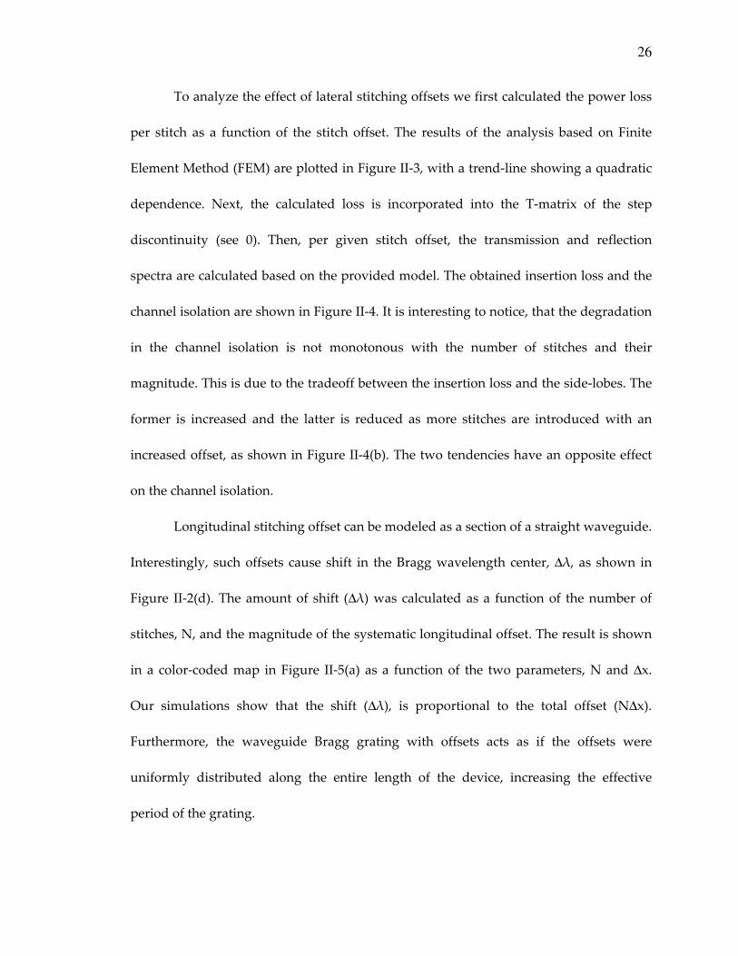
To analyze the effect of lateral stitching offsets we first calculated the power loss
per stitch as a function of the stitch offset. The results of the analysis based on Finite
Element Method (FEM) are plotted in Figure II-3, with a trend-line showing a quadratic
dependence. Next, the calculated loss is incorporated into the T-matrix of the step
discontinuity (see 0). Then, per given stitch offset, the transmission and reflection
spectra are calculated based on the provided model. The obtained insertion loss and the
channel isolation are shown in Figure II-4. It is interesting to notice, that the degradation
in the channel isolation is not monotonous with the number of stitches and their
magnitude. This is due to the tradeoff between the insertion loss and the side-lobes. The
former is increased and the latter is reduced as more stitches are introduced with an
increased offset, as shown in Figure II-4(b). The two tendencies have an opposite effect
on the channel isolation.
Longitudinal stitching offset can be modeled as a section of a straight waveguide.
Interestingly, such offsets cause shift in the Bragg wavelength center, ∆λ, as shown in
Figure II-2(d). The amount of shift (∆λ) was calculated as a function of the number of
stitches, N, and the magnitude of the systematic longitudinal offset. The result is shown
in a color-coded map in Figure II-5(a) as a function of the two parameters, N and ∆x.
Our simulations show that the shift (∆λ), is proportional to the total offset (N∆x).
Furthermore, the waveguide Bragg grating with offsets acts as if the offsets were
uniformly distributed along the entire length of the device, increasing the effective
period of the grating.
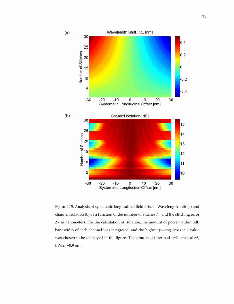
27
Figure II-5. Analysis of systematic longitudinal field offsets. Wavelength shift (a) and
channel isolation (b) as a function of the number of stitches N, and the stitching error
∆x in nanometers. For the calculation of isolation, the amount of power within 3dB
bandwidth of each channel was integrated, and the highest (worst) cross-talk value
was chosen to be displayed in the figure. The simulated filter had κ=40 cm-1, κL=6,
BW3dB=~0.9 nm.
(a)
(b)

28
Another manifestation of systematic longitudinal field offset is the degradation
in the channel isolation. Part of it is attributed to the shift in wavelength, and another
part to the appearance of additional resonances, observed in Figure II-2(d) in the form of
the increased side-lobes. To quantify the effect we calculated the amount of cross talk
between the desired channel and rest of the channels on the 1.6 nm grid.
The calculation was done by integrating the reflected power spectral density of
one channel over its own 3dB bandwidth and over the bandwidth of each of the other 20
channels in the grid. The ratio between the power integrated in the desired bandwidth
and the highest value of the power “spilled” into another channel is considered here as
the channel isolation. It is shown in Figure II-5(b) as a function of the number of stitches
and the magnitude of the longitudinal offset introduced in each stitch.
3.3. Discussion.
To evaluate manufacturability of long waveguide Bragg gratings with regard to
the stitching errors introduced in the fabrication process we distinguish between two
cases. First, consider a waveguide Bragg grating, fabricated with direct e-beam writing.
Since the critical dimension of waveguide Bragg gratings is on the order of 100 nm,
resolution of about 10 nm is required to assure good control over grating’s profile.
Existing e-beam writers achieve such resolution with write-fields as large as 500μm ×
500μm. As a consequence, the entire length of the grating (1.5 mm in our case) is
subdivided into several (3) write-fields, and stitching errors on the order of ~20nm or
below are to be expected. For such offsets, wavelength shifts below 0.1 nm and

29
degradation of channel isolation by <2 dB due to the longitudinal stitching errors, are
anticipated.
In the second case, we consider a Bragg grating fabrication using UV-lithography.
In this process the mask, created with an e-beam writer, is projected with some
demagnification onto the wafer coated with a UV-sensitive resist. The exposed resist is
developed and used as a mask for the following etching process, which transfers the
desired profile onto the wafer. Assuming demagnification factor of M, now an M-times
larger pattern needs to be written with an e-beam to create the UV mask. Assuming the
same e-beam write-field as in the previous case is used to write the mask, the grating
will have M-times more fields and M-times more stitches (3*M in our example), however
the same offset introduced in each stitch. After the mask is projected with M-times
demagnification, its image has M-times more stitches (3*M), however M-times smaller
stitching error (20/M nm). To be more specific, we assume M=3 such that the device in
our example will consist of ~9 stitches, with a typical offset of ~7nm. Wavelength shift
due to the stitching error is still below 0.1 nm, as shown in Fig 3a, and the channel
isolation is reduced by ~1.5 db, compared to an ideal Bragg grating, as shown in Fig 3b.
The significance of the effect of stitching on the performance of the Bragg
gratings depends on the application. For instance, dense WDM systems operate with
channel spacing of 25 GHz (~0.2 nm). Wavelength shifts of ~0.1 nm, caused by the
fabrication errors can therefore have a strong impact on the performance of a dense
WDM optical link. Some measures can be taken to mitigate these effects, including

30
pattern pre-distortion, optimized grating design, and minimization of the stitching
errors in the e-beam lithography. Fabrication requirements can be further relaxed, by
packing long gratings into a single lithographic field using a previously developed
approach [Zamek 2010]. The obtained results provide insights into the feasibility of
high-volume low-cost manufacturing of chip-scale photonic filters and multiplexers
based on Bragg gratings.
4. Curved Waveguide Bragg Grating.
In this Section we demonstrate miniaturization of waveguide Bragg gratings
using curved waveguide Bragg gratings, as shown in Figure II-6. An arbitrary Bragg
grating with a total length L can be packed into the desired area A using a cascade of
curved waveguide Bragg gratings. Using the same radius of curvature R for all sections
eliminates the need to adjust the period of the Bragg grating for each section separately,
as the dispersion relation is identical for all sections. It is easy to verify that the layout
Figure II-6. The proposed curved waveguide Bragg grating. (a) Dark-field
micrograph of the fabricated curved waveguide Bragg grating. (b) High
magnification SEM micrograph of a piece of the structure.
(a)
50 µm
(b)
2 µm

31
shown in the figure attains packing efficiency, defined as the dimensionless parameter
AL , of approximately R4Lπ .
Although more efficient packing schemes exist, it is obvious that smaller radius
of curvature is desirable. However, how small can the radius of curvature R be without
having an impact on the optical properties of the grating?
4.1. Model
To address this question, it is instrumental to consider a simpler structure,
consisting of a periodic array of curved waveguide Bragg gratings, depicted in Figure
II-7. Each section has a shape of an arc with radius R, and the junctions between the
sections are shown by broken red lines. These junctions are step discontinuities, where
some scattering occurs because of the mode mismatch in two consecutive sections. The
two sources of loss are therefore the scattering at the junctions and radiation losses due
to bending. As the radius of curvature gets smaller, both losses increase. We will next
Figure II-7. A cascade of curved waveguide Bragg gratings. (a) an example, and (b)
an equivalent device. Broken lines show planes of mode discontinuity where
scattering takes place.
(a) (b)

32
investigate the effect of decreasing the radius of curvature on the optical properties of
the Bragg grating.
The transmission coefficient through the cascade of N identical curved Bragg
gratings can be found using the Transmission Matrix approach. The Transmission
Matrix formalism is widely used in multi-port microwave networks and can be found in
textbooks [Harrington 1961]. Yamada and Sakuda applied it in the past to the analysis of
almost periodic gratings [Yamada 1987]. Following this approach, the field at any point
along the structure is given by the superposition of two counter-propagating modes
with amplitudes A and B . For a section of our structure, shown in Fig 1c, the modal
amplitudes at the input, iA and iB , can be related to those at the output, 1iA + and 1iB + ,
via the transmission matrix [Harrington 1961]:
( )
−
′′−′−=
=
−−
−−
+
+
i
i
11
11
i
i
1i
1i
B
A1
B
AT
B
A
trt
trtα, ( 1 )
where ii AB=r and i1i AA +=t (with 0B 1i =+ ) are the reflection and
transmission coefficients, and α is the power loss coefficient. From energy conservation,
it follows that 122
=++ αtr , and the determinant of the matrix equals unity. Eq 1
shows the general form of the transmission matrix of a reciprocal element. For more
discussion of the Transmission matrix, T, the reader is referred to 0. We will now find
the transmission matrices for the two elements comprising our structure – curved Bragg
gratings and the junctions between them.

33
For a section of curved waveguide Bragg grating of length bL , the coefficients r
and t in Eq. 1 can be found from the CMT [Yariv 1985]:
( )[ ]bb SLSjr coth+∆′−= βκ ( 2 )
( ) ( )[ ] 1coshsinh
−+∆= bbb SLSSLjSt β ( 3 )
where 22βκ ∆−=S , Λ−=∆ πββ , Λ is the Bragg grating period, κ is the coupling
coefficient, and β is the complex propagation constant of the mode. The transmission
matrix of a curved Bragg grating is given by
( )
−
′′−′−=
−−
−−
11
11
b
1T
bbb
bbbb
ttr
trtα, ( 4 )
The prime sign designates complex conjugate, and the subscript “b” stands for Bragg
grating. For zero losses ( β is real and 0=bα ) the result is in full agreement with
previous work [Yamada 1987].
The reflection and transmission coefficients, jr and jt , associated with the
junctions, are found numerically. For a small mode mismatch the transmission
coefficient is real and the reflection can be neglected [Marcuse 1972]. The transmission
matrix of a junction simplifies to
( )
−≈
10
011T
j
j
j
α
t, ( 5 )
34
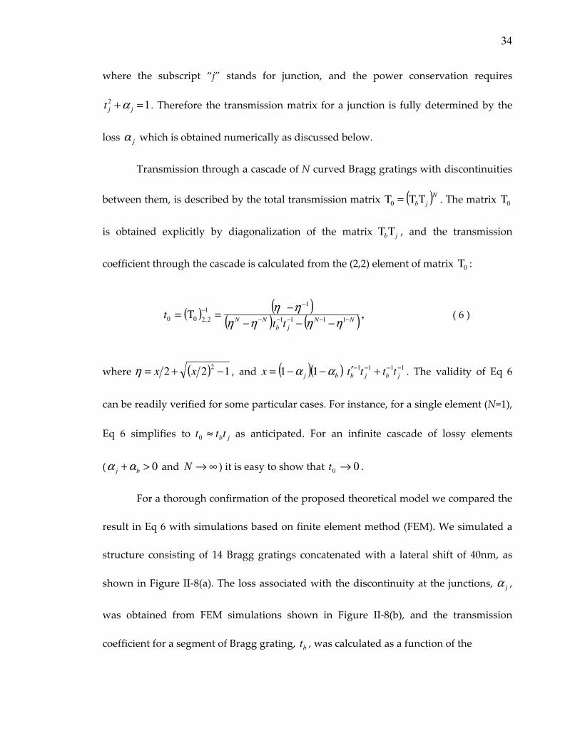
where the subscript “j” stands for junction, and the power conservation requires
12 =+ jjt α . Therefore the transmission matrix for a junction is fully determined by the
loss jα which is obtained numerically as discussed below.
Transmission through a cascade of N curved Bragg gratings with discontinuities
between them, is described by the total transmission matrix ( )N
jbTTT0 = . The matrix 0T
is obtained explicitly by diagonalization of the matrix jbTT , and the transmission
coefficient through the cascade is calculated from the (2,2) element of matrix 0T :
( ) ( )( ) ( )NN
jb
NNtt
t−−−−−
−−
−−−
−==
1111
11
2,200 Tηηηη
ηη, ( 6 )
where ( ) 1222
−+= xxη , and ( )( ) 111111 −−−− +′−−= jbjbbj ttttx αα . The validity of Eq 6
can be readily verified for some particular cases. For instance, for a single element (N=1),
Eq 6 simplifies to jbttt ≈0 as anticipated. For an infinite cascade of lossy elements
( 0>+ bj αα and ∞→N ) it is easy to show that 00 →t .
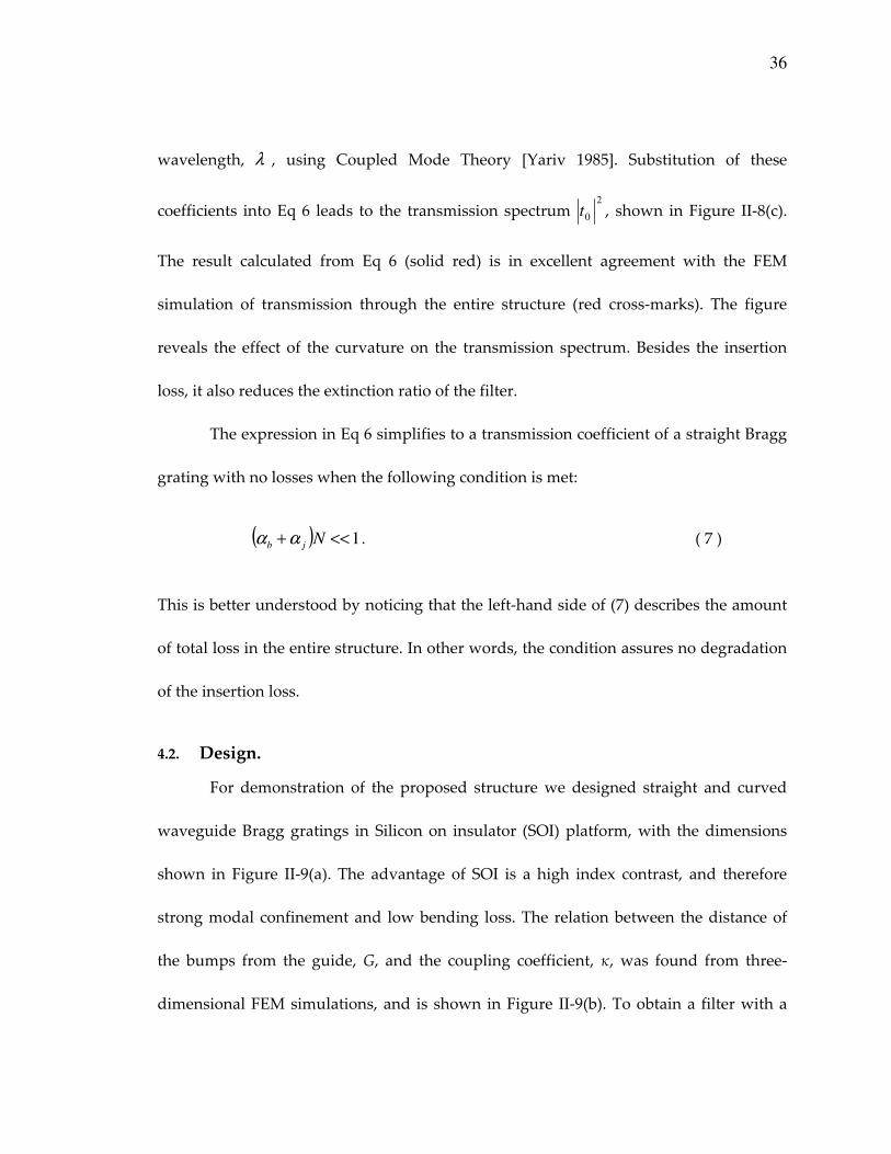
For a thorough confirmation of the proposed theoretical model we compared the
result in Eq 6 with simulations based on finite element method (FEM). We simulated a
structure consisting of 14 Bragg gratings concatenated with a lateral shift of 40nm, as
shown in Figure II-8(a). The loss associated with the discontinuity at the junctions, jα ,
was obtained from FEM simulations shown in Figure II-8(b), and the transmission
coefficient for a segment of Bragg grating, bt , was calculated as a function of the

35
Figure II-8. Confirmation of the model with FEM simulation. (a) Schematic of the
structure, showing a cascade of 14 sections concatenated with a lateral displacements
of 40nm. Each section is a Bragg grating waveguide, 200nm wide and 6.84μm long,
with refractive index n=3 and perturbation period of 342nm, giving coupling
coefficient of 0.22μm-1. (b) FEM simulation, used to obtain the transmission and loss
in the junctions. (c) Transmission of TE0 mode through the cascade of 14 Bragg
gratings, |t0|2, obtained from Eq 6 (solid red) vs. simulation result (black cross
marks). The reference curve (broken blue) shows the transmission through a straight
Bragg grating of the same total length with no breaks. The following parameters
were used in Eq 6: rj=αb=0, tj≈0.99, αj=0.02.
200nm 14 sections
total
342nm 20 periods
90nm
40nm
x z
|Ey|
(a)
(b)
(c)
36
wavelength, λ , using Coupled Mode Theory [Yariv 1985]. Substitution of these
coefficients into Eq 6 leads to the transmission spectrum 2
0t , shown in Figure II-8(c).
The result calculated from Eq 6 (solid red) is in excellent agreement with the FEM
simulation of transmission through the entire structure (red cross-marks). The figure
reveals the effect of the curvature on the transmission spectrum. Besides the insertion
loss, it also reduces the extinction ratio of the filter.
The expression in Eq 6 simplifies to a transmission coefficient of a straight Bragg
grating with no losses when the following condition is met:
( ) 1<<+ Njb αα . ( 7 )
This is better understood by noticing that the left-hand side of (7) describes the amount
of total loss in the entire structure. In other words, the condition assures no degradation
of the insertion loss.
4.2. Design.
For demonstration of the proposed structure we designed straight and curved
waveguide Bragg gratings in Silicon on insulator (SOI) platform, with the dimensions
shown in Figure II-9(a). The advantage of SOI is a high index contrast, and therefore
strong modal confinement and low bending loss. The relation between the distance of
the bumps from the guide, G, and the coupling coefficient, κ, was found from three-
dimensional FEM simulations, and is shown in Figure II-9(b). To obtain a filter with a
37
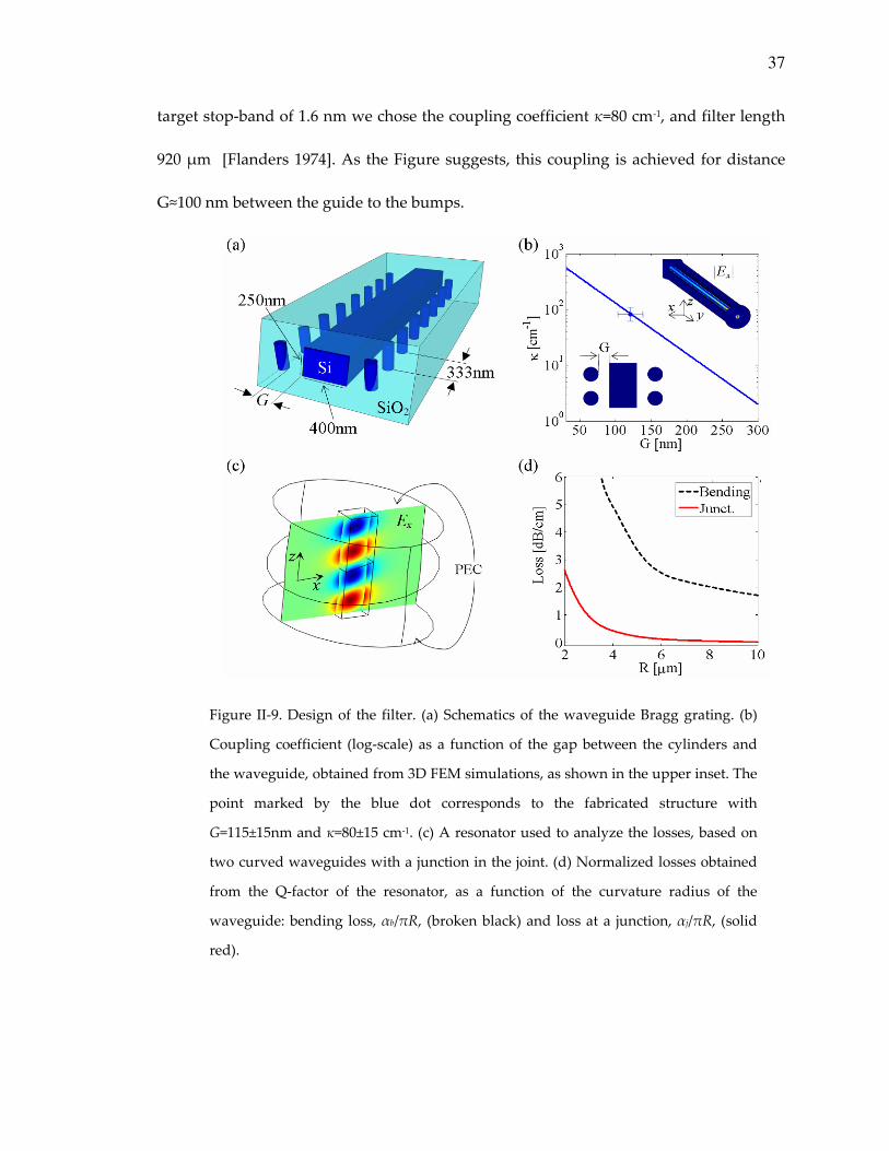
target stop-band of 1.6 nm we chose the coupling coefficient κ=80 cm-1, and filter length
920 μm [Flanders 1974]. As the Figure suggests, this coupling is achieved for distance
G≈100 nm between the guide to the bumps.
Figure II-9. Design of the filter. (a) Schematics of the waveguide Bragg grating. (b)
Coupling coefficient (log-scale) as a function of the gap between the cylinders and
the waveguide, obtained from 3D FEM simulations, as shown in the upper inset. The
point marked by the blue dot corresponds to the fabricated structure with
G=115±15nm and κ=80±15 cm-1. (c) A resonator used to analyze the losses, based on
two curved waveguides with a junction in the joint. (d) Normalized losses obtained
from the Q-factor of the resonator, as a function of the curvature radius of the
waveguide: bending loss, αb/πR, (broken black) and loss at a junction, αj/πR, (solid
red).

38
To analyze the losses (parameters bα and jα ) we simulated a resonator based on
two curved waveguides with a junction, depicted in Figure II-9(c). Perfect electric
conductors were used as its mirrors, so that the Q-factor is defined solely by the internal
losses. By comparing the Q-factors of a resonator with and without the junction, it is
possible to separate between the bending losses ( bα ) and losses due to discontinuity
( jα ), as explained in Appendix B. The results are shown in Figure II-9(d), where to
express the loss per unit length we normalized the parameters bα and jα by the factor
Rπ . As the Figure implies, radiation due to bending is the dominant source of loss for all
values of R. The radius of curvature was chosen to be R=19 μm, for which the total loss
is below 2 dB/cm, the fraction of power, jb αα + , lost at a segment with a circumference
of ≈= RLb π 60 μm is below 0.003, and for a total of N=15 segments condition (7) is
satisfied. Therefore, according to the developed analytical model, the structure should
exhibit a response identical to that of a straight grating of the same length.
4.3. Experiment.
The Bragg gratings were fabricated on SOI wafer, with Si thickness of 250 nm, on
top of a layer of thermal oxide with a thickness of 3 μm. First, negative tone resist was
patterned using an e-beam. Next, the resist was used as a mask for dry etching of Silicon.
The residual layer of the resist was removed by wet etching with diluted HF acid.
Finally, a layer of SiO2 with a thickness of ~2 μm was deposited on top as an upper
cladding using plasma-enhanced chemical vapor deposition (PECVD). Using this

39
technique, we fabricated straight and curved waveguide Bragg gratings with a total
length of 920 μm. Both structures had the same perturbation period Λ=333nm and the
same waveguide cross sections (250 nm high and 410±10 nm wide), as shown in Figure
II-10(a). To improve the coupling efficiency, the input and the output waveguides were
gradually tapered to the width of 110±10 nm. The sample was then diced and cleaved
across the tapered sections of the waveguide.
Transmission spectra were obtained by coupling a tunable laser source into the
tapered waveguides on the sample through a tapered polarization maintaining (PM)
fiber. The output waveguide of the device, also tapered, was imaged through a free-
space polarizer onto a detector connected to a power meter. Both the power meter and
the laser source were controlled by a computer, which recorded the detected power as
the wavelength of the tunable laser source was scanned in steps of 0.05 nm. The source
was linearly polarized and the PM fiber was aligned so that the electric field was parallel
to the sample plane to efficiently excite the TE-like mode.
The measured transmission spectra for the straight and curved Bragg gratings
are shown in Figure II-10(b) by red crosses and black dots, respectively. The measured
extinction ratio of both structures is higher than 23 dB, which is the limit, imposed by
the PM tapered fiber. Both gratings exhibit a stop-band width of 1.7 nm, which
corresponds to κ=90 cm-1. These parameters are slightly larger than those we used in the
design (1.6 nm and κ=80 cm-1), due to the deviation of waveguide widths from the
designed values. The two devices exhibit similar spectral response aside from the shift of

40
~2.6 nm, attributed to the dispersion of the bent waveguide. Since the dispersion of a
bent waveguide is known, this shift can be pre-compensated in the design to produce
the stop-band at the desired wavelength. The measured results are in good agreement
Figure II-10. Experimental results: (a) Fabricated devices. The boxes shown by
broken lines designate straight and curved waveguide Bragg gratings of the same
length. (b) Measured transmission spectra for straight (red crosses) and curved
(black dots) gratings. The solid lines show the fitted transmission spectra of Bragg
gratings with κ=90cm-1, ng=4.27, L=920μm, ne=2.340 for straight grating and ne=2.336
for curved grating, with a constant background 23 dB below the signal.
(a)
(b)
L
Curved Straight
2 µm 1 µm

41
with the analytical predictions made with the Coupled Mode Theory. More importantly,
aside from the offset, the curved Bragg grating has spectral response similar to that of a
straight grating, as predicted by the developed model.
To summarize, we demonstrated straight and curved filters based on waveguide
Bragg gratings. Both filters had a total length of 920 μm, a stop-band of 1.7 nm, and an
extinction ratio larger than 23 dB. The curved structure occupied an area of 190 μm × 114
μm, attaining packing efficiency AL ≈6.2. Nevertheless, it exhibited the same
performance as its straight counterpart. The proposed approach opens a route to avoid
stitching errors, present in the typical lithographic process of long structures. The
developed analytical model aims to assist design of such structures in the future.
5. Other Techniques for Folding.
An alternative technique for packing long waveguide Bragg gratings into a small
area on a chip is based on superstructure Bragg grating. Such structures were
extensively investigated in fiber-based configuration [Eggleton 1994, Sterke 1995,
Ouellette 1996, Broderick 1997, Kashyap 1999, Passaro 2002, Eggleton 2002]. The
structure consists of an array of waveguide Bragg gratings with spacers between them.
At first glance the structure reminds an array of coupled Fabry-Perot resonators with a
behavior different from the one expected from a waveguide Bragg grating. However it is
well known that upon certain conditions the structure exhibits behavior similar to that
of a straight waveguide Bragg grating with no spacers [Sterke 1995]. This phenomenon
can be easily explained by observing the corresponding T-matrix of the spacer. As it

42
follows from Appendix A, it is an eye-matrix, meaning that it plays no role in the
vicinity of the Bragg condition.
Figure II-11. An alternative for waveguide Bragg grating packing. (a) Super-structure
Bragg grating; (b) folded superstructure Bragg grating; (c) simulated transmission
spectrum for a structure with the parameters shown in the inset. The simulated
structure was a superstructure Bragg grating based on a 2D waveguide Bragg
grating with 14 sections each 6.84 μm long (=20Λ), with κ=220 cm-1, and TE-
polarization, as shown in the inset.
1.535 1.54 1.545 1.55 1.555 1.560
0.2
0.4
0.6
0.8
1
λ [µm]
Tra
nsm
issi
on
Ls=0
Ls=Λ
Ls=2Λ
(a)
(b)
(c)
Lb Ls
Λ

43
The superstructure Bragg grating shown in Figure II-11(a), has two fundamental
Fourier components with periods Λ and Λ0=Ls+Lb. Thus the reflection spectrum has
components at the sum and difference of the two fundamental frequencies. The new
reflection wavelengths are given by [Kashyap 1999]:
0
112
Λ+
Λ=
−b
en
λ, and
0
112
Λ−
Λ=
+b
en
λ ( 8 )
The bandwidth of the superstructure is defined by the coupling coefficient of the
single grating element. Eq 8 suggests that the superstructure has a response similar to
the response of a conventional Bragg grating without the blank spacers when the
differences between the wavelengths is significantly lower than the bandwidth of the
response, δλλλ <<− −+bb . The bandwidth is given by ωδωλδλ = , where e2 ncκδω =
[Yariv 1985]:
ee
2
nkn π
κλκ
ω
δω
λ
δλ=== ( 9 )
It would be interesting to investigate the applicability of the proposed folding
technique. More specifically, it seems possible to derive the conditions upon which the
superstructure behaves similarly to a conventional Bragg grating. Such a structure could
be used to pack long gratings into a small area as shown in Figure II-11(b). It would also
allow packing densities larger than those achieved by the method based on curved
waveguide Bragg gratings.

44
6. Other Applications.
Besides packing long waveguide Bragg gratings into a small area other
applications of the proposed curved waveguide Bragg gratings exist. One of them is a
Bragg grating incorporated into a ring resonator [Arbabi 2010, Kang 2010, Kang 2010]. It
was recently noted that Photonic crystal incorporated into a ring resonator might offer
advantages for slow photonics [Melloni 2009]. An intriguing feature of such a device is
that it is a hybrid of standing wave and traveling wave resonator. In one extreme, when
the reflection is strong enough, the micro-ring becomes a standing wave resonator, as no
power propagates in the ring. In the other extreme, if the grating is weak enough to
allow most of the power contained in the mode to pass through, the structure behaves as
a traveling wave resonator. This interesting feature requires further investigation.
7. Folding of 4-port devices.
Typical four-port device used for channel add/drop multiplexing is shown in
Figure II-12(a). These devices offer some benefits over other types of add/drop channel
multiplexers including larger FSR and smaller footprint. The difficulty in folding such
four-port waveguide Bragg grating arises from the fact that the radius of curvature
cannot be preserved along each waveguide. Varying curvature means varying the
dispersion relation which is manifested as a shift in Bragg wavelength. To avoid this
difficulty it seems possible to apply the technique depicted in Figure II-12(b), similar to
the one suggested for 2-port devices. Following this technique dispersion elements are
inserted as shown in Figure II-12(c). The task in hand then is to design these elements so

45
that the transmission spectrum of the structures depicted in Figures (a) and (c) are
identical.
Figure II-12. Folding of four-port devices. (a) Channel add/drop multiplexer. (b)
Four-port analog of a superstructure Bragg grating. (c) Potential technique for
folding four-port structures. Blocks ‘A’ and ‘B’ designate dispersion compensation
elements.
(a)
(b)
(c) A
B
46
The text of this Chapter, in part or in full, is a reprint of the material as it appears in the
following journal publication:
S. Zamek, D.T.H. Tan, M. Khajavikhan, M. Ayache, M.P. Nezhad, and Y.
Fainman, “Compact chip-scale filter based on curved waveguide Bragg
gratings”, Opt. Lett., 2010, 35, 3477-3479,
The dissertation author was the primary researcher and author. The co-authors listed in
this publication directed and supervised the research which forms the basis for this
chapter.

- 47 -
III. Integrated Metallic Mirrors.
Previous Chapter discussed routes to folding long Bragg gratings that provide
narrow-bandwidth response. The proposed folding techniques were demonstrated to
allow packing long structures into small areas on a chip. This chapter explores wide
bandwidth reflectors and investigates technique for their miniaturization. Integrated
metallic mirrors are suggested and their applicability to the construction of micro-
resonators is considered. Such reflectors allow miniaturization of micro-scale structures
by yet another order of magnitude and more. Two configurations are explored
theoretically and experimentally in SOI platform: 2D slab waveguide terminated by
metallic mirrors, and channel waveguide terminated by metallic mirrors coupled to a
bus waveguide.
1. 3D Configuration.
1.1. Introduction
Optical micro-resonators are promising candidates for miniaturization of free-
space and fiber-based devices. Such resonators have sparked enormous interest due to
the advantages they offer in the areas of biochemical sensing [Armani 2007], chip-scale
interconnects [Preble 2007], sub-wavelength lasers [Mizrahi 2008, Nezhad 2010], signal
processing [Zhang 2010], and communications [Baba 2008]. The silicon on insulator
(SOI) platform is especially appealing as it offers (1) strong confinement of light due to
high index contrast between silicon and the oxide, (2) ready integration of photonics

48
with micro-electronics, and (3) high-volume production, leveraging the existing CMOS
fabrication infrastructure [Pavesi 2004]. Examples of recently studied silicon based
micro-resonators include microrings [Little 1998, Dumon 2004, 2006], microdisks
[Koonah 2005, Morand 2006], and cavities with distributed Bragg reflectors (DBRs) [Kim
2007, Kim 2007].
Waveguide-coupled resonators can be subdivided into two major families:
traveling wave and standing wave resonators. Traveling wave resonators are typically
based on microdisks, microrings, and micro-toroids [Vahala 2004, Heebner 2008].
Standing wave resonators include photonic crystals, quarter-wave-shifted gratings, or,
simply, a waveguide terminated with DBR [Haus 1984, Joannopoulos 1995]. DBRs seem
to be the most popular ones due to their high reflectivity along with easy fabrication
process, however DBRs have several limitations. First, they are polarization sensitive, as
transverse-electric (TE) and transverse magnetic (TM) modes of a waveguide exhibit
different guided indices and therefore generally do not satisfy Bragg condition for the
same wavelength. Second, DBR’s smallest feature size is in the deep sub-micron regime,
which requires state-of-the-art fabrication facilities and tools with good process
repeatability.
Metallic mirrors overcome some of these limitations. The advantages of metallic
mirrors are low polarization sensitivity, compactness, and high tolerances to fabrication
imperfections. Despite their wide use in the free-space optical components, metallic
mirrors found just a few applications in guided wave optics. This is due to the high

49
anticipated losses of such mirrors when integrated into a high-index waveguides
[Coldren 1995]. In chip-scale devices, metallic mirrors have only been integrated with
low-index materials such as polymer [Wolff 2001] and silica [Shibata 2004] waveguides.
In our previous work [Zamek 2010] we demonstrated the feasibility of high Q-factors in
silicon micro-resonators constructed with metallic mirrors. Such mirrors were shown to
allow dense chip-scale integration of resonators and to relax the fabrication
requirements. In this work we demonstrate a micro-resonator with metallic mirrors
made in a SOI platform, coupled to a bus waveguide, as shown in Figure III-1(a). An
analytical model for a side-coupled resonator is developed and the design tradeoffs are
investigated.
1.2. Description of the Device
A schematic of the device is shown in Fig 1a. SOI platform was used to realize Si
waveguides resting on a SiO2 substrate. The resonator is based on a channel silicon
waveguide with a cross-section identical to the cross section of the bus waveguide. The
resonator’s waveguide is terminated with two metallic plates, creating a cavity. The
resonator is side coupled to a channel (bus) waveguide. The upper cladding of the
device is silicon dioxide, which is not shown on Fig 1a for clarity. The resonator’s length,
Lr, is the distance between the mirrors, and Lc is the length of the coupling region, where
the gap between the two waveguides is uniform (Lr ≥ Lc).
When an optical mode propagates in the bus waveguide, some of its energy will
couple into the resonator by the mechanism of co-directional evanescent coupling [Yariv

50
1985]. It will further circulate in the resonator, reflecting off the mirrors. Assuming low
coupling between the two waveguides, this will generally have a negligible effect, with
most of the power transmitted through the bus waveguide. If the resonance condition is
satisfied, even a small coupling will cause a buildup of an intense field in the resonator.
Some of this field will couple back into the bus resonator and will destructively interfere
with the incident mode propagating in the waveguide. As we show below, at resonance
this effect can result in an appreciable dip in the transmission spectrum and strong
reflection back into the bus waveguide.
Figure III-1. The proposed device: (a) Schematic of the studied device. (b) Illustration
of the formalism used to construct the analytical model.
51
It is important to emphasize the differences between the suggested device and
traveling wave resonators such as rings, disks, and toroids. Standing-wave resonator,
such as the one depicted in Figure III-1(a), exhibits high reflectance and low
transmittance on the resonance. This is in contrast to traveling-wave resonators with all-
pass behavior. The advantages and possible applications of standing-wave resonators
were extensively studied in previous works [Kazarinov 1987, Haus 1992, Manolatou
1999, Xu 2000, Lohmeyer 2002, Hammer 2004]. High-Q resonators employed DBRs,
while low-Q resonators used cleaved waveguide facets. So far, metallic mirrors received
little or no attention in guided wave optics, despite their extensive use in free-space
optics. In the following section we derive the analytical model for a resonator with
metallic mirrors side coupled to a bus waveguide.
1.3. Analytical Model
Analytical approaches for the analysis of waveguide-coupled resonators include
rigorous solution of four coupled modes equations [Kazarinov 1987], coupling of modes
in time [Haus 1992], and scattering-theory formalism [Xu 2000]. Here we took an
approach based on multiple reflections model, analogous to the one used for the
analysis of Fabry-Perot interferometer. The approach relies on the fact that the
transmission spectrum of an optical filter can be obtained by summing the signals
arriving from all the possible paths from the input to the output [Madsen 1999]. The
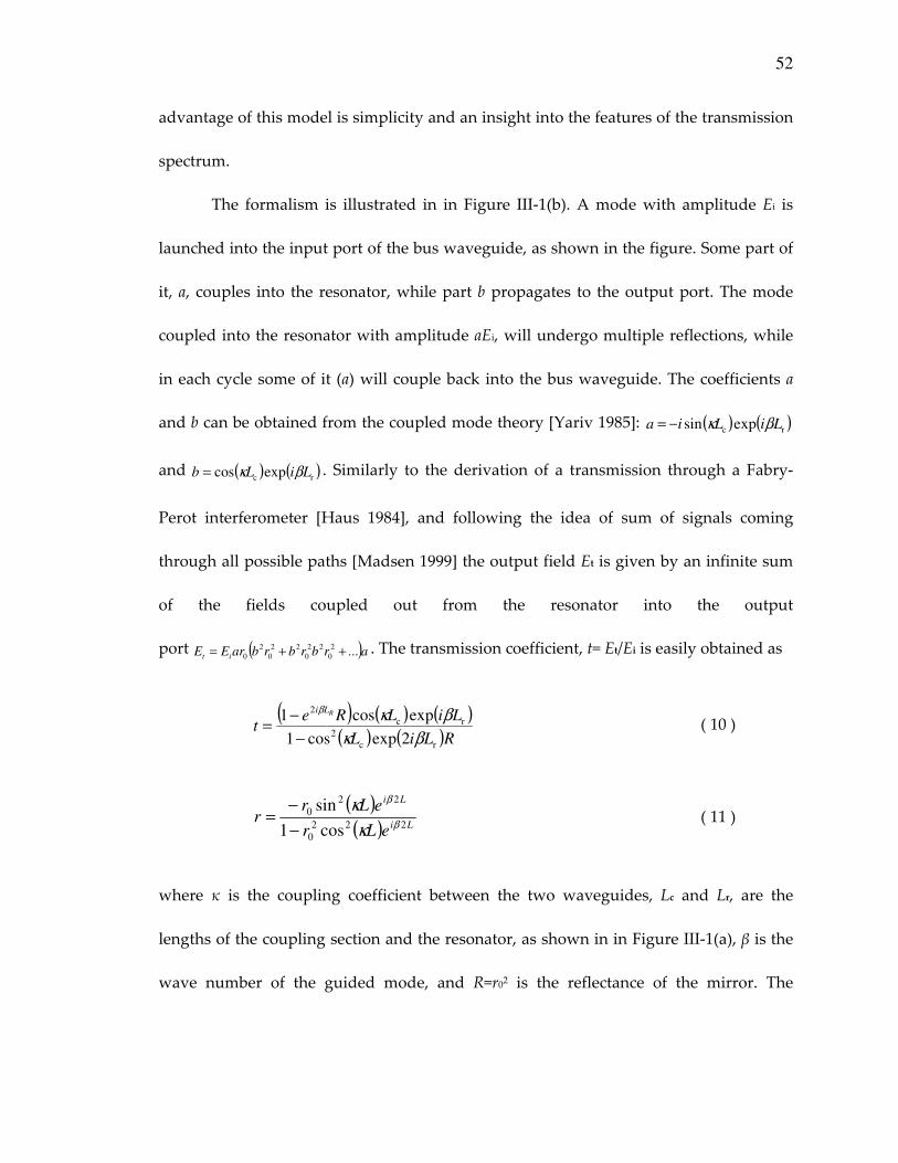
52
advantage of this model is simplicity and an insight into the features of the transmission
spectrum.
The formalism is illustrated in in Figure III-1(b). A mode with amplitude Ei is
launched into the input port of the bus waveguide, as shown in the figure. Some part of
it, a, couples into the resonator, while part b propagates to the output port. The mode
coupled into the resonator with amplitude aEi, will undergo multiple reflections, while
in each cycle some of it (a) will couple back into the bus waveguide. The coefficients a
and b can be obtained from the coupled mode theory [Yariv 1985]: ( ) ( )rc expsin LiLia βκ−=
and ( ) ( )rc expcos LiLb βκ= . Similarly to the derivation of a transmission through a Fabry-
Perot interferometer [Haus 1984], and following the idea of sum of signals coming
through all possible paths [Madsen 1999] the output field Et is given by an infinite sum
of the fields coupled out from the resonator into the output
port ( )arbrbrbarEE it ...2
0
22
0
22
0
2
0 ++= . The transmission coefficient, t= Et/Ei is easily obtained as
( ) ( ) ( )
( ) ( )RLiL
LiLRet
RLi
rc
2
rc
2
2expcos1
expcos1
βκ
βκβ
−
−= ( 10 )
( )( ) Li
Li
eLr
eLrr
222
0
22
0
cos1
sinβ
β
κ
κ
−
−= ( 11 )
where κ is the coupling coefficient between the two waveguides, Lc and Lr, are the
lengths of the coupling section and the resonator, as shown in in Figure III-1(a), β is the
wave number of the guided mode, and R=r02 is the reflectance of the mirror. The

53
expression in Eqs 10 and 11 were confirmed with 2D simulations based on the Finite
Element Method (FEM). In these simulations we considered a TE-mode, 200 nm wide
waveguide, side-coupled to a resonator with the coupling coefficient of κ=560 cm-1.
Three resonators with Lc=Lr=5,10, and 15μm, terminated with mirrors with reflectivity
R=0.95 were simulated and full agreement between the equations and the simulation
results was obtained.
To obtain the Q-factor of the resonator, we expand the propagation constant in
the vicinity of a resonance as gv/0 ωββ ∆+≈ , where
gv is the group velocity of the mode.
After the result is substituted into Eq 10, the transmittance is obtained:
( ) ( )( ) ( )
( )( ) ( )2
r
2
c
21
2
r
21
c
22
2cos
21cos
g
g
vLLR
vωLRLt
ωκκω
∆+−
∆+−≈
−
−
( 12 )
On the other hand it is well known that a waveguide side-coupled to a resonator
exhibits a transmission spectrum of the general form [Xu 2000]:
( ) ( ) ( )( ) ( )22
C0
22
02
ω
ωω
∆+Γ+Γ
∆+Γ=t ( 13 )
Here Γ0 and ΓC are the mode decay rates associated with the internal resonator losses,
and losses due to the coupling of the resonator to a waveguide. Comparison of Eqs (12)
and (13) reveals the factor cos2(κLc), which appears in Eq 12 but not in Eq 13. This factor
is due to the difference between previous research [Xu 2000] and this work in the choice
of reference planes, where Ei and Et are defined (see in Figure III-1(a)). If the input and

54
the output reference planes were chosen at the center of the resonator, as it was done in
Ref 26, the factor would disappear from Eq (12). Aside from this factor, Eqs (12) and (13)
are equivalent, where the decay rates Γ0 and ΓC and the associated Q-factors are given
by:
12 1
r0
0
0−
=Γ
=−
R
LnkQ
gω , ( 14 )
( )c
2
r0
c
Csin2 L
LnkQ
g
κ
ω=
Γ= ( 15 )
Here k0= ω/c, and ng is the group index of the waveguide mode. We note that Q0 is the
unloaded Q-factor independent of the coupling losses. The total Q-factor is calculated as
1/Q=1/Q0+1/QC.
It is interesting to notice, that the two Q-factors associated with the coupling and
the mirror losses are both dependent on the resonator length, but in an opposite manner,
as shown in Figure III-2(a). For extremely short cavities the coupling is negligible and
the Q-factor is dominated by the mirror losses. For long cavities, the coupling happens
over a longer length, leading to a larger mode decay rate, and the Q-factor is dominated
by the coupling. To confirm the results obtained in Eqs 14 and 15 we performed 2D FEM
simulations as shown in Figure III-2(b-d). The Q-factors were calculated from the
eigenmodes found from the simulations, with the simulation results

55
Figure III-2. Confirmation of the model. (a) Q-factors as a function of normalized
length of the resonator L/λ calculated from Eqs 14 and 15. Q-factor associated with
the external coupling (QC), mirror losses (Q0), and the total Q-factor (QT) are shown
by broken blue, dashed black, and solid black correspondingly. The black cross-
marks show FEM simulation results of the coupled resonator. (b-d) Electric field
|Ez| distribution as obtained from FEM simulations for L/λ=0.22, 1.33, and 3.54
(where L=Lr=Lc). All simulation used TE polarization with the following parameters:
mirror reflectivity R=0.98, normalized coupling coefficient κλ=0.114, normalized
separation distance between the resonator and the bus waveguide G/λ=0.26, and
normalized thickness of the waveguides d/λ=0.13.
Ez| ⊗⊗⊗⊗
(a)
(b)
(c)
(d)

56
shown in Figure III-2(a) by black cross-marks. Good agreement between simulations and
analytical results was found, confirming the validity of our model.
Another important characteristic of the coupled micro-resonator, is the extinction
ratio (ER). ER is defined as the ratio of the transmittance in the pass-band to the one on
the resonance. To derive it, we should notice here that at resonance exp(2iβLr)=1 in Eq 10.
This happens when βLr=πm, where m is an integer describing the longitudinal mode
number. Exactly in the middle between two resonances βLr=π(m+0.5) and therefore
exp(2iβLr)=-1. By substitution of these two into Eq 10, the ratio between the two
transmittances can be calculated and the ER is found:
( )( )
2
c
2
c
2
cos1
cos1
1
1
+
−⋅
−
+=
LR
LR
R
RER
κ
κ ( 16 )
It is interesting to notice that for no coupling between the resonator and the bus
waveguide, i.e. κ=0, ER approaches 1, as anticipated. This case is equivalent to a straight
waveguide, for which the transmission equals 1 over the entire spectrum above the
waveguide’s cutoff frequency. On the other hand, when the reflectivity R approaches 1,
the ER tends to infinity. From this discussion it becomes evident that the coupling loss
must predominate over the internal resonator loss to achieve high ER. In other words,
large ratio Q0/QC is required to attain large ER.
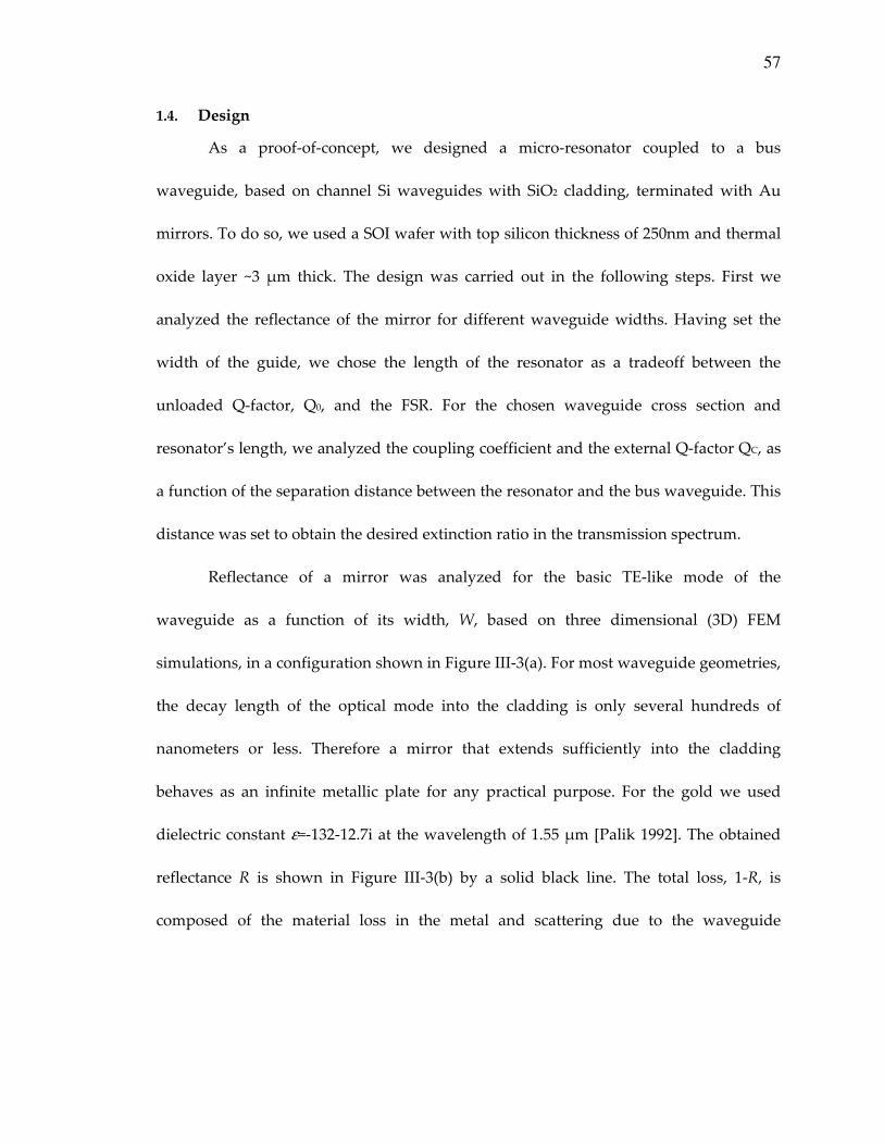
57
1.4. Design
As a proof-of-concept, we designed a micro-resonator coupled to a bus
waveguide, based on channel Si waveguides with SiO2 cladding, terminated with Au
mirrors. To do so, we used a SOI wafer with top silicon thickness of 250nm and thermal
oxide layer ~3 μm thick. The design was carried out in the following steps. First we
analyzed the reflectance of the mirror for different waveguide widths. Having set the
width of the guide, we chose the length of the resonator as a tradeoff between the
unloaded Q-factor, Q0, and the FSR. For the chosen waveguide cross section and
resonator’s length, we analyzed the coupling coefficient and the external Q-factor QC, as
a function of the separation distance between the resonator and the bus waveguide. This
distance was set to obtain the desired extinction ratio in the transmission spectrum.
Reflectance of a mirror was analyzed for the basic TE-like mode of the
waveguide as a function of its width, W, based on three dimensional (3D) FEM
simulations, in a configuration shown in Figure III-3(a). For most waveguide geometries,
the decay length of the optical mode into the cladding is only several hundreds of
nanometers or less. Therefore a mirror that extends sufficiently into the cladding
behaves as an infinite metallic plate for any practical purpose. For the gold we used
dielectric constant ε=-132-12.7i at the wavelength of 1.55 μm [Palik 1992]. The obtained
reflectance R is shown in Figure III-3(b) by a solid black line. The total loss, 1-R, is
composed of the material loss in the metal and scattering due to the waveguide

58
discontinuity introduced by the mirror. The relative contribution of scattering to the
total loss is shown by broken blue line on the same figure.
Figure III-3. Theoretical investigation of the mirror. (a) Schematic of an Au mirror
inserted into a Si waveguide. (b) Mirror’s reflectance, R, (solid black) and the ratio of
scattering loss to the total loss (broken blue) as a function of guide’s width, W. An
inset shows the considered cross-section of the waveguide. The shaded area
corresponds to W below 150nm, for which the results are inaccurate due to the high
numerical error of FEM, associated with low mode confinement. All results pertain
to TE-like mode and a wavelength of λ=1.55μm.

59
To understand the result we consider two extremes. In the first extreme, W
approaches zero, the mode is poorly confined, and most of the power flows in the
cladding. This case resembles reflection of a plane wave normally incident onto the Au-
SiO2 interface, for which the reflectance equals ~0.975. In the other extreme, where W is
sufficiently large, the mode is
Figure III-4. Theoretical investigation of the micro-resonator. (a) Effective and group
index, ne and ng, as a function of waveguide’s width, W. (b) Coupling coefficient, κ,
as a function of the gap, G, between the guides, for the geometry shown in the inset.
All results pertain to TE-like mode and a wavelength of λ=1.55μm.
(a)
(b)

60
strongly confined to the core of the waveguide, and the reflectance approaches ~0.95,
which is the reflectance at the Au-Si interface. For W=280 nm, the reflectance reaches its
minimum value of ~0.78, associated with strong scattering. For this geometry most of the
loss is attributed to the scattering, as shown by the broken blue line in Figure III-3(b). A
width W=400 nm was chosen to provide both high reflectance R=0.9, and high group
index ng=4.27, as shown in Figure III-3(b) and Figure III-4(a).
The length of the resonator, LR, is a tradeoff between the Free Spectral Range
(FSR) and the Q-factor. The FSR is given by λ2/2Lrng [Zamek 2010]. We chose the length
to be Lr=13.4 μm, leading to FSR of 21 nm, making it possible to observe several resonant
lines with the setup described below. Such length resulted in an unloaded Q-factor of
Q0=2100 at the wavelength of λ=1.55 μm, as given by Eq 14. The total Q-factor is
dominated by the external Q-factor, Qc, which is calculated below.
Next we consider two waveguides with a cross section 250nm×400nm, separated
by a distance G, as shown in the inset of Figure III-4(b). To analyze the coupling
coefficient, κ, we separately used the expressions provided in Refs [Haus 1984] and
[Buckman 1992]. The field profile used in the calculations was obtained from FEM
simulations. Both results designated ‘H’ and ‘B’ obtained from each of the references are
shown in Figure III-4(b) correspondingly. The results were also confirmed using the
technique described in Appendix G. For the chosen distance G=240nm, the coupling is
κ=1400cm-1, the external Q-factor Qc~300, and the extinction ratio of the transmission
spectrum is approximately 20 dB, as obtained from Eq 16. To summarize, our design

61
targeted the following parameters of the micro-resonator coupled to a bus waveguide:
Q0=2100, QC=300, FSR=21nm, and ER=20dB at the wavelength of 1.55μm.
1.5. Fabrication
The step-by-step fabrication process is illustrated in Figure III-5. We first used
electron beam lithography (EBL) to pattern Hydrogen SilsesQuioxane (HSQ) resist on a
SOI wafer. The created pattern was used as a mask for dry etching of silicon, resulting in
Si waveguides on top of a SiO2 layer. The residual HSQ was removed by 10 sec wet
etching in a diluted (1:10) buffered oxide etch (1:6 BOE solution). A layer of polymethyl
methacrylate (PMMA) resist was patterned on top using an overlay EBL. The patterned
PMMA was used as a mask for the second dry etching of silicon, and a successive dry
etching of silicon dioxide, opening gaps for the mirrors in the Si waveguides. Electron
beam evaporation of gold with a consecutive liftoff
Figure III-5. Conceptual illustration of the fabrication process. The two panes show
two different cross-sections of the device (XY in the upper pane and ZY in the lower
pane, as shown). The dimensions are not up to scale.

62
in acetone left gold plugs inserted into the Si waveguide. This created a resonator
composed of a Si waveguide side coupled to a bus waveguide as shown in Figure III-6.
A layer of SiO2 with a thickness of 2 μm was deposited on top using plasma-enhanced
chemical vapor deposition (PECVD). The fabricated device and its parameters are
shown in Figure III-6(b).
1.6. Experiment
To measure the transmission spectrum we used a telecom-grade linearly polarized
tunable laser source. Its output was coupled into an on-chip waveguide through a
tapered polarization maintaining fiber. The fiber was affixed to a 5-axis mechanical stage
to allow precise alignment between the fiber and the waveguide. The output port of the
waveguide was imaged through a polarizer onto the detector, connected to a power
meter. The polarizer was set to pass the electric field parallel to the plane of the sample,
to efficiently excite TE-like mode of the waveguide. The reading of the power meter was
recorded as the wavelength of the source was scanned in steps of 20 pm. The obtained
power spectrum of the transmission through the bus waveguide is plotted in Figure III-7
by red dots. The solid black curve shows the analytical result as calculated from Eq 10
for the parameters used in the design.
The obtained transmission spectrum exhibits several interesting features. First, it
shows a ripple of approximately 2 dB, which is a result of interference created by mode
reflection off the cleaved facets of the
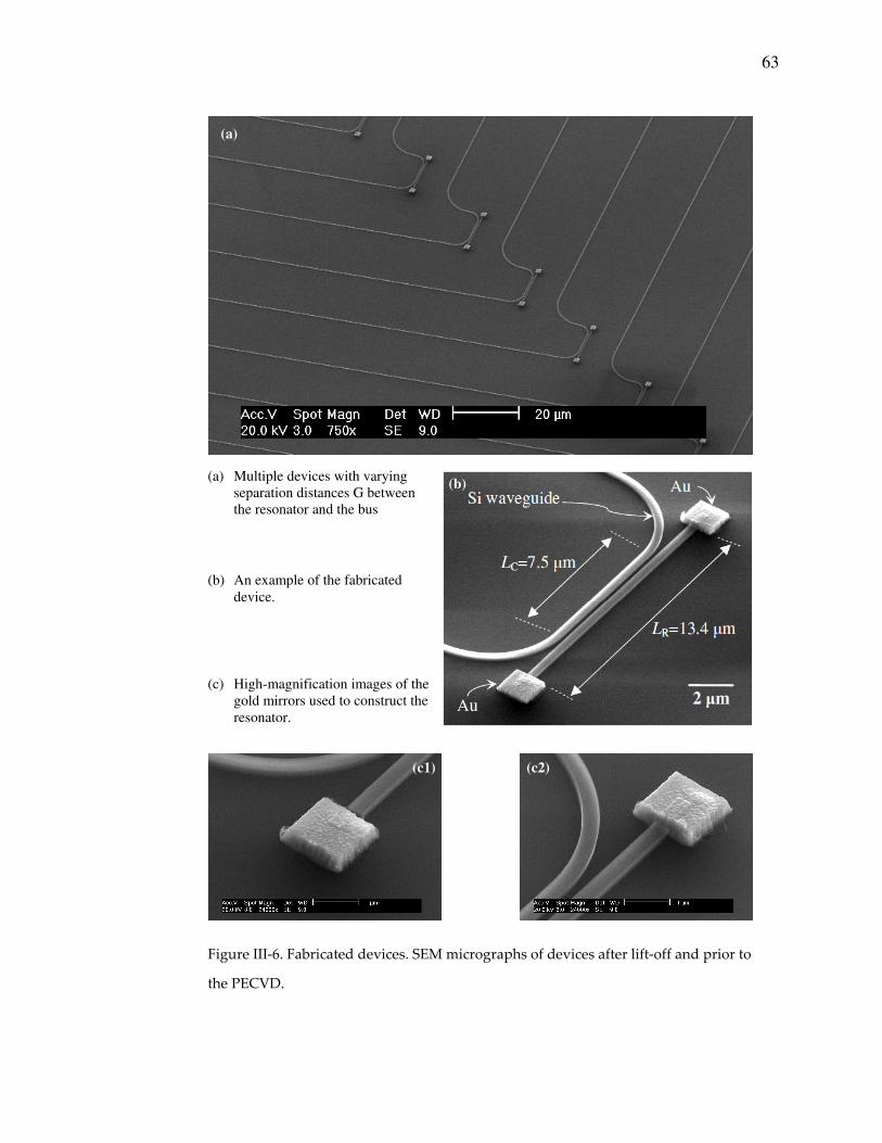
63
Figure III-6. Fabricated devices. SEM micrographs of devices after lift-off and prior to
the PECVD.
(a) Multiple devices with varying
separation distances G between
the resonator and the bus
waveguide.
(b) An example of the fabricated
device.
(c) High-magnification images of the
gold mirrors used to construct the
resonator.
(a)
(c1)
(b)
(c2)

64
Figure III-7. Experimental (red dots) and simulated (solid black) transmission spectra
of TE-like mode of the fabricated device in dB.
waveguide. Second, it shows a FSR~21 nm, which is in agreement with the analytical
prediction. The ER grows towards longer wavelengths, due to poorer mode confinement
and larger coupling between the two waveguides. The experimentally obtained
extinction ratio ER~10 dB is significantly lower than the analytical value (~20 dB). This is
due to several factors, listed here in the order of their significance: mirror reflectivity
R~0.8 lower than anticipated (~0.9) due to fabrication imperfections, smaller coupling
coefficient κ (~1200cm-1 instead of 1400cm-1) due to narrower waveguides, depolarization
of the mode due to the coupling between TE- and TM-like modes at waveguide bends
and perturbations created by the mirrors, reduced refractive index of the upper cladding
created by PECVD process, and polarization extinction ratio in the excitation of the
waveguide by a tapered fiber. To summarize, the fabricated device exhibited QC=360

65
instead of 300 (by design) and Q0=900 instead of 2100, providing a total Q-factor of 260.
According to these parameters, the insertion loss is ~0.7dB as estimated from Eq 10.
The mirror quality, which is the dominant factor among those listed above, is
compromised by the roughness, tilt, and conformity to the waveguide facet. The
roughness is introduced in the dry-etching of Si through a mask of PMMA, with its
typical values on the order of ~10 nm peak-to-peak. The roughness of the deposited
metal is significantly increased outside of the silicon waveguide due to the lift-off
process. However the rough surface of metal is believed to play minor role as most of
the power flows in the Si waveguide, where the roughness is minimal since no contact
between metal and the resist was established. The tilt of the mirror is about 7 degrees as
estimated from the SEM images. This tilt is due to the shadowing of the evaporated
metal by the PMMA resist.
1.7. Discussion.
The described fabrication process can be improved to reduce the roughness and
the tilt of the mirror. Evaporation of metal at an angle can be done to reduce the tilt and
to increase the conformity of the mirror to the waveguide. PMMA can be replaced with
other resists that offer higher sidewall smoothness. Adding post-fabrication processing,
such as rapid thermal annealing, can smooth the mirrors’ rough surface. Also other
fabrication techniques can be investigated.
High mirror reflectivity R is critical to obtain high finesse, narrow resonance line
width, and high extinction ratio, desirable in many applications. Our design was
66
constrained by the height of the Si waveguide (250 nm), set by the availability of SOI
wafers. In practice, the guide cross section can be optimized to achieve reflectivity of
0.95, as suggested by Fig 3b. Even higher reflectivity (up to 0.975) can be obtained on the
expense of mode confinement by significantly decreasing the cross section of the
waveguide, and pushing the mode out into the cladding, as suggested by the same
figure. Nevertheless, the inherent material loss limits the reflectivity to ~97.5%,
corresponding to the maximum finesse of ~120. Such losses do not exist in DBRs, whose
reflectivity approaches unity for a sufficiently large number of periods.
The reflectivity of metallic mirrors cannot compete with the conventional DBRs.
Nor can the resonator achieve the Q-factors of the state-of-the-art resonators with small
mode volumes [Mizrahi 2008, Srinivasan 2003, Gérard 1998, Xia 2010, Preston 2009]. The
major strength of metallic mirrors, however, rests with their ability to provide
reasonably high reflectivity over a broad band of wavelengths and low polarization
sensitivity. In addition, the optical skin depth in metal is on the order of 10 nm, so that a
very thin layer of metal is sufficient to achieve the desired reflectivity. Hence the
proposed metallic mirrors can attain extremely small footprints, by an order of
magnitude smaller than those of a typical DBR. DBR’s smallest feature size is in the deep
sub-micron regime and requires a high degree of fabrication accuracy. Metallic mirrors,
in contrast, impose no such constraints and exhibit low sensitivity to fabrication
imperfections.

67
1.8. Improving the Q-factor.
The Q-factor of the resonator is defined by two losses – losses in the mirrors and
external coupling losses, due to leakage of power into the bus waveguide. Both Q-factors,
Q0 and QC can be improved. While the external Q-factor QC, can be made infinite by
sufficient separation between the resonator and the bus waveguide, the internal Q-factor
is not easily improved. As Eq 14 shows, the internal Q-factor, Q0, is defined by the group
index and the reflectivity of the mirrors. The reflectivity R can be increased up to 0.976
by optimizing the waveguide cross-section and giving up mode confinement, as
discussed in section 1.4.
For low confinement the reflectivity is defined by the reflectivity of a plane wave
on the boundary between the metal and the dielectric used in the cladding. Therefore
use of lower index dielectric as a cladding would allow reflectivity higher than 0.98. The
lowest available refractive index is ~1.338 for Poly (tetrafluoroethylene-co-
hexafluoropropylene) at a wavelength of 5893Ӑ [Brandrup 2005]. Its refractive index in
the near-IR is even lower, due to the typical material dispersion. However even for the
lowest index material, with a refractive index of ~1.29 [Groh 1991], the reflectivity only
improves to 0.979. For the lowest possible refractive index, n=1 (vaccum), the reflectivity
increases to 0.984, which is still insufficient for applications that require high finesse.
This brings about the major drawback of metallic reflectors, which have an inherent
material loss, compromising the optical performance.

68
The more promising direction is improving the Q-factor by increasing the group
index, ng. In photonic crystal waveguides (PCW), for instance, group velocity decreases
to zero close to the band edge [Joannopoulos 1995]. Practically it is limited by the
fabrication imperfections, which are on the order of several nanometers with the current
micro-fabrication technologies [Baba 2008]. Significant enhancement was shown by
using such structures, where ng was as high as several hundreds [Joannopoulos 1995,
Vlasov 2005, Baba 2008]. Such a structure consists of a slow-light waveguide terminated
with metallic mirrors. Micro-resonator 1μm long with ng=100 and R=0.97, exhibits an
unloaded Q-factor of ~12,000. Practical interest in such structures is questionable due to
the following drawbacks. First, use of PCW requires high performance fabrication tools,
undermining the major advantage of metallic mirrors. Second, PCW is polarization
dependent, which again revokes the advantage of metallic mirrors. Nevertheless, PCW
terminated with metallic mirrors pose interest and must be further investigated.
1.9. Summary
To summarize, we demonstrated a micro-resonator based on silicon waveguide
terminated with metallic mirrors. The mirrors are compact and highly reflective. The
geometry was optimized to achieve an unloaded Q-factor of 2100 for a resonator 13.4
μm long. Its measured transmission spectrum was in good agreement with the
developed analytical model. The device may be used to construct high-order inline
filters, spectrum shapers, true-time delays, modulators, channel add-drop multiplexers,
and biochemical sensors.

69
2. 2D Configuration.
So far we considered metallic mirrors in 3D configuration, relevant to
waveguide-based devices. In this section we show that integrated metallic mirrors can
also be used in the 2D configuration, which is appealing for label-free biochemical
sensing. The application of biochemical sensing discussed in details in Appendix I, was
the primary motivation for the work summarized below.
2.1. Introduction.
During the past decades optical micro-cavities found a large variety of
applications in the fields of communications, display technologies, and biochemical
sensing [123][Vahala 2003, Doan 1992, Cooper 2002]. Realization of these devices using
silicon-on-insulator (SOI) material platform will take advantage of the existing low-cost
microelectronics manufacturing, making it particularly appealing for various
applications of future optoelectronic systems. Aside from the numerous applications in
Silicon Photonics, optical micro-cavities are strong candidates for the replacement of
fluorescence based arrays in biochemical sensing, thereby reducing time and cost of
drug development, environment monitoring, and medical diagnostics [Cooper 2002]. In
this regard, planar resonators allow dense integration of multiple devices on a SOI
platform, and are therefore especially suitable for chip-scale high-throughput
biochemical sensor arrays. Such resonators can be constructed using distributed Bragg
reflectors (DBR) [Tan 2009], Photonic Crystals [Kim 2007], or simply by cleaved
waveguide facets.
70
Here we introduce an on-chip resonator made of a silicon waveguide terminated
with metallic mirrors, and a grating coupler to allow excitation of the guided modes
from free space, as shown in Figure III-8. Such mirrors have the benefit of high
reflectivity for all transverse waveguide modes at an arbitrary wavelength. As a proof of
concept we fabricated a 40μm long resonator, which exhibited a quality factor (Q) of
about 1000, and a free spectral range (FSR) of 8.1nm. Application of this resonator to
label-free biochemical sensing is considered, and its surface sensitivity to adsorption of
molecules (e.g. proteins) is investigated and optimized. The resulting ultra-high
sensitivity enables detection of a sub-nanometer monolayer of molecules, which is
comparable to large grating couplers [Tiefenthaler 1989, Schmid 2009], thus allowing
their miniaturization.
2.2. Device Description.
The resonator, shown in Figure III-8(a), consists of a thin silicon (Si) film (n=3.48)
on top of a silicon dioxide (SiO2) substrate (n=1.46). Aluminum (Al) mirrors are inserted
into a Si waveguide, creating a resonator for the modes propagating along the x-axis. A
grating is patterned onto the Si guiding layer to facilitate excitation of the guided modes
from free space. Provided the y-dimension of the resonator is sufficiently large, a simpler
two-dimensional (2D) model may be adopted, as shown in Figure III-8(b).

71
Figure III-8. Geometry of the metallic cavity. (a) Si slab waveguide (Si thickness d)
with partial Al mirrors separated by distance L. A grating with a period Λ on top of
the Si layer is used for the excitation of the guided modes in the Si layer. (b)
Conceptual 2D model, used throughout the document.
The resonator modes satisfy two phase relations for the optical field: (1) the
dispersion relation of a slab waveguide given by
( )0 effk nβ λ= , ( 17 )
where β is the propagation constant of the waveguide mode, 0k is the free space wave
number, corresponding to wavelength λ , and ( )λeffn is the dispersion relation of the
waveguide, and (2) the longitudinal resonance imposed by the metallic mirrors, given
by
L mβ π= , ( 18 )
where L is the resonator length, and m is an integer designating the longitudinal mode
number.

72
Figure III-9. Resonator design considerations. (a) Illustration of the two equations for
the resonator modes. (b) Group index as a function of waveguide thickness. (c)
Reflectivity of the partial Al mirror as a function of the waveguide thickness. (d)
Surface sensitivity for the proposed resonator. The red dots in (b)-(d) designate the
fabricated resonator, and the inset in (c) shows FEM simulation of |Hy| in this case.
To derive the FSR we represent the set of Eqs. 17 and 18 as curves in the λβ −
plane. The lowest waveguide modes, TE0 and TM0, are of special interest since they
exhibit higher confinement, higher reflectivity off the mirrors, and higher surface
sensitivity [Tiefenthaler 1989]. Their dispersion relation, Eq. (17), is plotted in Figure
III-9(a), assuming the thickness to be d=250 nm, and the resonator length to be L=3 μm
for a lucid illustration. The condition for a longitudinal resonance is shown by three

73
dashed lines. The intersection points correspond to the eigenmodes of the resonator, and
the distance between them is the FSR, designated by λ∆ on Figure III-9(a). Linearization
of the dispersion curve yields:
1
g
2
22
−
−≈∆
Ln
L
λλλ , ( 19 )
where ( ) λλλ ∂∂−= effeffg nnn is the group index of the mode, shown in Figure III-8(b)
as a function of d. The strong dependence of the FSR on the slab thickness is thus
evident. For long cavities ( λ>>L ), Eq. (19) simplifies to 2
g2Lnλ λ∆ ≈ , which is a well
known result in the field of diode lasers [Nathan 1963].
The Q-factor of the resonator in the 2D model may be expressed as
1 1 1
m gQ Q Q− − −= + , where mQ and gQ correspond to the losses of the mirrors and the
grating, respectively. To obtain mQ , the reflectivity R of the Al mirror as a function of
the slab thickness d is obtained using Finite Element Method (FEM), assuming
235 42.5 jε = − − as the permittivity of Al at λ=1.55 μm, for time dependence of
exp( )j tω [Palik 1985]. The results are shown in Figure III-8(c) for the two lowest
waveguide modes TE0 and TM0. mQ is then given by [Yariv 1989]
( )g
m 1
2
ln
LnQ
R
π
λ −= , ( 20 )

74
such that mQ is determined by both the group index and the reflectivity shown in
Figure III-8(b) and (c) correspondingly.
Figure III-10. Q-factors for the two polarizations: TE (left) and TM (right) as functions
of the normalized geometry parameters, L and d, as shown in the inset.
2.3. Design.
The device was designed for operation with the TM0 mode, which is favorable
for biochemical sensing, as shown below. The resonator was fabricated on a SOI wafer
with d=250 nm thickness of the top Si layer, which corresponds to a group index
43.4g =n at λ=1550 nm, and mirror reflectivity R=0.76, as seen in Figure III-8(b) and (c).
The distance between the mirrors was chosen to be L=40 μm resulting in FSR=7 nm, so
that the finite grating length allows excitation of at least two resonances within the
tuning range of the laser source, without changing the incidence angle. The
d/λ d/λ
L/λ

75
corresponding quality factor is 2600m =Q . A Hydrogen Silsesquioxane (HSQ) e-beam
resist was used to create a grating with a period of 600 nm, whose (-1) diffraction order
was used to excite TM0 mode of the waveguide from free space. The Q-factor due to the
radiation losses of the grating (n=1.36) is found from FEM simulations to be Qg≈3000.
The total Q-factor of the resonator is calculated to be about 1400. The y-dimension of the
resonator was chosen to be 200y =L μm, so that the diffraction losses in the x-y plane
(see in Figure III-8(a)), do not significantly degrade this value of Q.
2.4. Fabrication.
The fabrication consisted of three major steps. First, PMMA was used as an etch mask to
define the mirrors on the SOI wafer. Next, RIE etching was performed, followed by e-
beam evaporation of Al with a consecutive lift-off, forming a waveguide terminated
with Al mirrors. Finally, a grating was created by patterning HSQ resist on top of the
resonator. Unlike the previous fabrication process, discussed in Section 1.5, here we did
not etch the SiO2 substrate, so that the mirrors did not protrude beneath the Si layer.
This simplified the fabrication process, explained in details in Appendix D. Microscope
and SEM micrographs of the fabricated device are shown in Figure III-11.

76
Figure III-11. Fabricated device. (a) SEM micrograph of the resonator, showing the
mirrors and the grating on top of a Si waveguide. The mirrors were coated with HSQ
resist to prevent their oxidation. (b) High magnification SEM micrograph showing
the grating profile. (c) Micrograph of the entire resonator obtained with an optical
microscope.
2.5. Experiment.
To evaluate the performance of the cavity we used a tunable CW laser source
with a wavelength scanning range from 1520 to 1570 nm and a resolution of 1 pm. A
beam with a diameter of 0.5 mm was incident upon the cavity at an angle of ~21 degrees
to the normal through a polarizer set to excite the TM0 mode of the waveguide. An
objective with a magnification of 10x was used to image the cavity onto a detector. The
setup is shown in Figure III-12. The power reflected off the cavity as a function of the
wavelength was recorded with a power meter, as shown by the red dots in Figure
III-13(a). The reflection spectrum exhibits a typical asymmetrical resonant line-shapes
L=40µm
(a) 250nm 600nm
(b)
Ly=200 µm
(c)

77
[Glasberg 1998, Fan 2003, Hwang 2008], which correspond to the excitation of cavity
modes. For characterization of the optical properties of the cavity, the data was fitted to
a sum of Fano line-shapes imposed on a linear background:
( ) ( )[ ]( ) ( )∑ = Γ+−
−+Γ++=
2,1 22
2
2
2i
ii
iiiqbaR
λλ
λλλ , ( 21 )
where iλ and iΓ are the centers and the widths of the resonances, respectively, and iq
are their asymmetry parameters. The result of the model fitting is shown in Figure
III-13(a) by the black curve, with the estimated parameters specified on the plot. The Q-
factors calculated from the fitted parameters are about 860 and 970 for the first and the
second resonance, respectively. These are below the theoretical value (Q~1400), obtained
from the 2D model due to diffraction losses in the cavity plane and mirror imperfections.
Significantly higher Q-factors are feasible for the same cavity size with TE mode, thicker
Si waveguide, and improvement of the mirror quality.
The reflection spectrum was simulated using FEM. Both experimental and
simulated results were fitted to the above-mentioned model, and the linear background
was removed from both for comparison. The two reflection spectra with their fitted
model parameters are shown in Figure III-13(b). The experimental FSR (~8.1 nm) differs
from the one predicted by the 2D model (~7 nm), due to an out-of-plane diffraction by
the grating. For different wavelengths, the propagation direction of the excited
waveguide modes slightly rotates in the cavity plane, causing a deviation from Eq 19,
which presumes mode propagation normal to the mirrors.

78
Figure III-12. Experimental setup. top (a) and front (b) views. Schematic setup is
shown in (c). Shown in the figure: (1) tunable laser source, (2) fiber collimator, (3)
polarizer, (4) aperture, (5) sample under test, (6) imaging lens, (7) apertures with
micrometer, (8) detector, (9) detection arm, (10) illumination arm, (11) translational
stages, (12) rotational stages.
Power
Meter Source
PC
Detector Optical Setup
(a)
(b)
(c)
1
2
3
4
6 5
7
8
9 10 11
12

79
Figure III-13. Experimental results. (a) Reflection spectrum of the cavity with metallic
mirrors: measured data (red dots) and the fitted model (black curve). The inset
shows the measured (red dots) and the fitted (black curve) reflection spectrum for a
200μm x 200μm grating without the mirrors, for comparison. (b) Comparison of the
experimental results (solid black) with the simulated 2D model (dashed blue)
reflection spectrum. The experimental data was normalized by an incident power,
and the linear background was removed from both the simulated and the
experimental data for a vivid comparison of the two results.
For a demonstration of the benefit of the proposed metallic mirrors, we
compared the resonances of the fabricated cavity with those of a larger grating without
the mirrors. To do so we fabricated a 200 μm x 200 μm grating on the same SOI platform,

80
with the same grating profile as the one used in the cavity. The measured reflection
spectrum for the grating is shown in the inset of Figure III-13(a). Although the area of
this grating is 5 times as large as that of the cavity, the Q-factors of the cavity are higher
than those of the grating which has Qg≈740, showing a clear benefit of the metallic
mirrors.
It is worth emphasizing here that for a grating, the resonances are dictated only
by the phase-matching condition between the incident and the guided waves in k-space,
whereas for a cavity the resonances are discrete wavelengths derived from Eqs. 17 and
18.
2.6. Application to Biochemical Sensing.
We next consider application of the proposed micro-cavity to label-free
biochemical sensing. Capability of label-free detection of biochemical molecules is of
extreme importance in pharmaceutical industries, medical diagnostics, and
environmental monitoring [Homola 2006]. Grating couplers, in particular, were shown
do achieve ultra-high sensitivity, making it possible to detect sub-nm layers of bound
proteins [Tiefenthaler 1989]. It was also shown that the high-index waveguide is crucial
to achieve high surface sensitivity of the guided mode, which makes SOI a good
candidate for on-chip biochemical sensing [Schmid 2009]. It is shown above that the
proposed micro-cavity exhibits Q-factors as large as those of large gratings. Next we
show that this miniaturization is possible without compromising the high surface
sensitivity.

81
The sensing is based on the shift in the resonant wavelength due to the presence
of a biochemical substance that is adjacent to the cavity waveguide. We therefore
assume that a thin layer with refractive index np=1.45 and thickness h adsorbs onto the
surface of the cavity from water (n~1.33), which constitutes the upper cladding of the
waveguide. This alters the dispersion relation neff(λ) of the waveguide and therefore
perturbs the cavity’s resonant wavelengths. The surface sensitivity hS ∂∂≡ λλ is
obtained by assuming ( )hnn ,effeff λ= in Eqs. 17 and 18, and their differentiation with
respect to h:
1
geff −
∂
∂=
∂
∂≡ n
h
n
hS λ
λλ . ( 22 )
Here hn ∂∂ eff is the sensitivity of the effective index of the guided modes in an infinite
slab waveguide, which was obtained analytically [Tiefenthaler 1989]. The sensitivity of
the cavity, Sλ, is shown in Figure III-4(d). The maximum sensitivity is Sλ~0.5 and it is
obtained for TM0 mode in a waveguide with thickness (d~0.2λ). In that case, upon
adsorption of an adlayer with a thickness h, the resonant wavelengths will shift by 0.5h.
For our setup the SNR is sufficiently high (>30dB), and the detection limit is given by the
wavelength repeatability of the tunable laser source [Hwang 2008]. With the current
repeatability δλ~15pm, the minimum variation in the thickness of an adlayer that can be
detected is ∆h~2δλ/Sλ~60pm. This is two orders of magnitude smaller than the typical
thickness of protein monolayers and corresponds to ~4 ng/cm2 surface mass coverage
[Feijter 1978]. Such sensitivity is appealing not only for biochemical sensing, but also for

82
environmental monitoring, where detection of extremely small molecules may be
desired. Further performance enhancement is possible with improved wavelength
repeatability and cavity design.
High throughput biochemical sensing is required by many applications such as
drug discovery, genome sequencing, warfare, food quality control, and environmental
monitoring. In those applications the assay must be checked for a presence of dozens
and sometime thousands of different biochemical species. These applications require
parallel biochemical detection of various molecules on a sensor array. Micro-arrays
based on fluorescent assays are widely used today for that purpose. Some efforts are
under way to make label-free micro-arrays [Schena 2005, Kambhampati 2004, Cooper 2009].
Figure III-14 shows how the proposed micro-resonator can be used in such an array to
allow high-throughput label-free biochemical sensing.
Figure III-14. Concept of high-throughput label-free biochemical sensing.
To the camera Illumination
Beam

83
Following the concept depicted in Figure III-14, an array of micro-resonators is
illuminated by a wide collimated beam. The array is imaged onto a camera. As the
wavelength of the illumination source is scanned, images are acquired with the camera
for each wavelength. By integrating the intensity of the acquired images within the area
of each resonator, reflectivity spectrum is obtained on every time interval. Monitoring
the shifts in the dip of the reflection spectrum over time, kinetics of the reaction can be
investigated (see for example the chapter by Navratilova and Myszka in [Homola 2006]).
Using a standard label-free detection scheme allows detection of certain molecules in the
analyte.
2.7. Summary.
We presented a novel type of chip-scale resonators, formed by a planar dielectric
waveguide terminated with metallic mirrors. The simplified 2D model for such a
resonator was developed and predicted the Q-factor and FSR in good agreement with
the experimental results. The proposed mirrors exhibit low spectral sensitivity, high
reflection for arbitrary polarization and different transverse waveguide modes. The
resonator was optimized to enable detection of the smallest molecules adsorbing to its
surface. The ultra-compact size of the metallic mirrors, and the high fabrication
tolerances are promising for future chip-scale high-throughput label-free biochemical
sensor arrays, as well as other applications in Silicon Photonics.

84
3. Metallic Mirrors - Discussion.
Metallic mirrors have been believed to have very high losses when integrated
into high-index waveguides. This work offers the first thorough investigation of metallic
reflectors in two geometries (2D and 3D). An interesting feature of the reflection
spectrum is revealed by numerical simulations of such mirrors, showing strong
degradation of the reflectivity for some waveguide cross-sections. Therefore careful
design must be carried out when building such a device. A number of useful devices
based on metallic reflectors were demonstrated both theoretically and experimentally,
including an inline filter and biochemical sensor. More potential applications were
discussed and future research directions were suggested. Metallic mirrors were shown
to exhibit low polarization sensitivity, high reflectivity to multiple transverse waveguide
modes, and high tolerance to fabrication imperfections.
The text of this Chapter, in part or in full, is a reprint of the material as it appears in
S. Zamek, L. Feng, M. Khajavikhan, D.T.H. Tan, M. Ayache, Y. Fainman, “Micro-
Resonator with Metallic Mirrors Coupled to a Bus Waveguide“, Optics Express 19 (3),
2011,
and
S. Zamek, A. Mizrahi, L. Feng, A. Simic, Y. Fainman, “On-chip waveguide resonator
with metallic mirrors”, Optics Letters, 2010, 35, 598-600.
The dissertation author was the primary researcher and author. The co-authors listed in
this publication directed and supervised the research which forms the basis for this
chapter.

- 85 -
IV. Future research directions
1. Folded Waveguide Bragg Gratings
Additional techniques for folding waveguide Bragg gratings were discussed in
Section 5 of Chapter II. The four-port analogue of the conventional superstructure Bragg
gratings, depicted in Figure II-12 is appealing as it allows packing densities higher than
those achieved with the demonstrated technique. To the best of my knowledge such
structure has not been investigated and is therefore interesting from both theoretical and
practical perspectives. Possible research in this direction can include derivation of the
condition for the dispersion element that must be satisfied to resemble the response of
the conventional contra-directional coupler.
2. Graphical Methods for Solving Complex Structures.
In Section 1.3 of Chapter III we demonstrated an analytical technique for
calculation of transmission through a waveguide side-coupled to a resonator. Instead of
solving multiple coupled mode equations with different boundary conditions, we used
graphical representation of the propagation of an optical signal. By graphically mapping
out all the possible paths the signal takes in the system, the transmission spectrum was
calculate. This technique can be generalized to more complex structures, with multiple
standing and traveling wave resonators coupled together. To do so, graphical diagram
depicting all the possible signal paths must be constructed. Further, methods for
simplification of those diagrams must be developed. Similarly to other fields of

86
engineering, such as set theory, control flow, and computer science, such diagrams can
prove handy for fast solution of complex problems.
3. High-Q Resonators with Metallic Mirrors
In Section 1 of Chapter III we considered a micro-resonator with metallic mirrors.
The advantages of metallic mirrors are: low polarization sensitivity, high reflectivity
over broad band of wavelengths, reflectivity of multiple transverse waveguide modes,
and compactness. It would be interesting to investigate the following directions.
Q-factor can be enhanced by using a slow light waveguide. Slow light
waveguide can based on PhC looses the major advantages of metallic mirrors, which are
low sensitivity to polarization and wavelength, and high tolerances to fabrication
imperfections. The tradeoffs between the desired qualities mentioned above and the Q-
factor enhancement must be further investigated. It is also instrumental to investigate
the phenomenon of strong coupling between the guided wave to a scattered one,
causing significant degradation in the reflectivity of the mirror for some waveguide
cross section geometries, as shown in Figure III-3(b). This effect might be mitigated by
the proper design of the metallic mirror. Coating the metal with a low-index dielectric
will also lead to an enhanced reflectivity.
Another interesting direction is making the filter, suggested in Section 1 of
Chapter III, polarization independent. That would make the device appealing for fiber-
communications, where polarization independency is a crucial feature. While reflection
off a metal exhibits low sensitivity to polarization, integrated metallic mirrors do show

87
polarization dependency. Also the coupling between the bus waveguide and the micro-
resonator is polarization sensitive. It is therefore an interesting challenge with a number
of practical implementations to design a polarization independent device.
Traveling wave resonators, such as microrings, microdisks, and toroids, are
popular elements for channel add-drop multiplexing. Standing wave resonators were
shown to be able to perform this function in some configurations [Manolatou 2002]. It is
an interesting task to compare the performance of OADM based on traveling and
standing wave resonators. Differences between the suggested micro-resonator with
metallic mirrors and its counterparts can be further investigated. Applicability of the
resonator to gain equalization and dispersion compensation are also of practical interest.
Vernier effect can be used to construct an infinite-finesse resonator based on the
following scheme. Two resonators coupled to a bus waveguide act as wavelength
dependent reflectors, creating a resonant cavity. Two resonators with different lengths
can be designed to be resonant at the wavelength of interest. Due to different lengths
such mirrors would have different FSR, and therefore a different grid of resonant lines.
Therefore the combination of the two resonators would only have a single frequency
band where both resonators will exhibit resonance and therefore create a high-Q cavity.
It is of practical interest how an infinite finesse can be obtained by the proposed
technique.

88
4. Transformer Based on Through-Coupled Resonator.
In Section 1 of Chapter III we considered a micro-resonator side-coupled to a bus
waveguide. It was shown previously that if such micro-resonator is through-coupled
with a waveguide, the reflection assumes the shape of the transmission spectrum and
vice versa [Kazarinov 1987, Haus 1984, Xu 2000]. Therefore the proposed micro-
resonator can not only perform resonant reflection, but also resonant transmission. In
other words it can be used as an inline filter. It would be interesting to investigate
performance metrics of such a device and the tradeoffs of its characteristics.
5. Group Delay Dispersion.
In Chapters II and III we considered the response spectrum of the proposed
resonant structures. When applied to communication systems, the group delay of a filter
and its dispersion are of extreme interest as they define the maximum useful bandwidth
of the entire system [Agrawal 2004]. It is interesting therefore to evaluate the group
delay dispersion of the proposed structures and compare it to other types of micro-
resonators. Ways to compensate the group delay dispersion of the filter are also of
practical interest.

- 89 -
V. Summary of the Thesis
This work investigated routes to miniaturization of chip-scale devices such as
reflectors, filters, resonators, and multiplexers. As a case study we explored folding of
waveguide Bragg gratings to allow fitting long structures into small areas on a chip and
performance and applicability of metallic reflectors for the construction of high-Q micro-
resonators. We also investigated applications of these structures for communications
and biochemical sensing. The proposed techniques allow smaller footprints, denser
integration, easier layout, and higher manufacturability. Although the techniques were
demonstrated on a specific case study, the developed methods are applicable to more
general set of devices.
The work falls into a more general effort of miniaturization of chip-scale
photonic circuits. Such miniaturization promises to revolutionize information
technologies and the life sciences. In information technologies, photonic circuits can
resolve the interconnect bottlenecks in computing and communications. These can foster
personal high-power computing, higher connectivity with large bandwidth aggregation
close to the consumer. In the life sciences, integrated chip-scale photonics can facilitate
point-of-care diagnostics and personalized medicine. Outlook far into the future
suggests strong impact on our lives and the society as a whole.

- 90 -
References
[1] Agrawal G.P., Lightwave Technology – Components and Devices, Wiley 2004.
[2] Arbabi A., Kang Y. M., and Goddard L., "Cylindrical coordinates coupled mode theory," IEEE J. Quant. El. 46, 1769–1774, 2010.
[3] Armani A. M., Kulkarni R. P., Fraser S. E., Flagan R. C., and Vahala K. J., “Label-free, single-molecule detection with optical microcavities”, Science 317, 783-787 (2007)
[4] Assefa S., Schow C., Xia F., Green W. M. J., Rylyakov A., and Vlasov Y., “CMOS integrated optical receivers for on-chip interconnects,”, EEE J. of Selected Topics in Quantum Electronics 16 (5), pp. 1376-1385 (2010).
[5] Baba T., “Slow light in photonic crystals”, Nature Photonics 2, 465-473 (2008).
[6] Boyd J. T., Integrated optics: devices and applications, IEEE Press 1991.
[7] Born M. and Wolf E., Principles of optics: electromagnetic theory of propagation, interference
and diffraction of light, 7th ed., Cambridge 1999.
[8] Bragg W.L., The diffraction of X-rays by crystals, Nobel Lecture, September 6, 1922.
[9] Bragg W. H., “X-rays and Crystals.” Nature, 90 (1912), 219.
[10] Bragg W. L., ’The Diffraction of Short Electromagnetic Waves by a Crystal“, Proceedings of the Cambridge Philosophical Society. Mathematical and Physical Sciences, 17 (1912), 43 -57
[11] Brandrup J., Immergut E. H., Grulke E. A., Abe A., Bloch D., Eds., Polymer Handbook, 4th ed., Wiley 2005.
[12] Broderick N. G. R. and de Sterke C. M., “Theory of grating superstructures”, Phys. Rev. E 55, 3634–3646 (1997).
[13] Brongersma M. L., Kik P. G., Surface plasmon nanophotonics, Springer 2007, pp. 1-2.
[14] Buckman A.B., Guided Wave Photonics, Saunder College Publishing 1992, pp. 149-154.
[15] Chang W. S.C., Guided-Wave Optoelectronic Devices, Cambridge 2009.
[16] Coldren L. A., Corzine S. W., Diode lasers and photonic integrated circuits, Wiley & Sons 1995, ch. 3.
[17] Coppola G., Irace A., Cutolo A., and Iodice M., “Effect of fabrication errors in channel waveguide Bragg gratings”, Appl. Opt. 38 (1999), pp. 1752-8.

91
[18] Cooper M. A., Label-free biosensors: techniques and applications, Cambridge University Press 2009.
[19] Cooper M., “Optical Biosensors in Drug Discovery”, Nature Reviews Drug Discovery 1, 515-528 (2002).
[20] Crowell B. The Modern Revolution in Physics, 3d ed., 2005, ch. 3.
[21] Dagenais M., Leheny R.F., Crow J., Integrated optoelectronics, Academic Press 1995.
[22] Davis J., Meindl J. D., Eds., Interconnect technology and design for gigascale integration, Kluwer Academic Publishers 2003.
[23] De Feijter J.A., Benjamins J., and Veer F.A., “Ellipsometry as a tool to study the adsorption behavior of synthetic and biopolymers at the air-water interface”, Biopolymers 17, 1759-1772 (1978).
[24] de Sterke C. and Broderick N., "Coupled-mode equations for periodic superstructure Bragg gratings," Opt. Lett. 20, 2039-2041 (1995).
[25] Doan V. V. and Sailor M. J., “Luminescent Color Image Generation on Porous Si”, Science 256, 1791-2 (1992).
[26] Dumke W. P., “Interband Transitions and Maser Action”, Phys. Rev. 127, 1559–1563 (1962).
[27] Dumon P., Bogaerts W., Wiaux V., Wouters J., Beckx S., Van Campenhout J., Taillaert D., Luyssaert B., Bienstman P., Van Thourhout D., and Baets R., “Low-loss SOI photonic wires and ring resonators fabricated with deep UV lithography”, IEEE Phot. Tech. Lett. 16, 1328-30 (2004).
[28] Ebeling K. J., Integrated optoelectronics: waveguide optics, photonics, semiconductors, Springer-Verlag 1993.
[29] Eggleton B.J., Krug P.A., Poladian L. , Ouellette F., “Long periodic superstructure Bragg gratings in optical fibres”, El. Letters 30, 1620 – 1622 (1994).
[30] Erickson D., Optofluidics, in S. Kakaç, Microfluidics Based Microsystems: Fundamentals and
Applications, pp 529-551.
[31] Fainman Y., Lee L., Psaltis D., Yang C., Optofluidics: fundamentals, devices, and applications, McGraw Hill 2010.
[32] Fan S., Suh W., and Joannopoulos J., “Temporal coupled-mode theory for the Fano resonance in optical resonators”, J. Opt. Soc. Am. A 20, 569-572 (2003).
[33] Flanders D. C., H. Kogelnik, R. V. Schmidt, and C. V. Shank, “Grating filters for thin-film optical waveguides”, Appl. Phys. Lett. 24, 194 (1974).

92
[34] Gérard J. M., Sermage B., Gayral B., Legrand B., Costard E., and Thierry-Mieg V., “Enhanced spontaneous emission by quantum boxes in a monolithic optical microcavity”, Phys. Rev. Lett. 81, 1110–1113 (1998).
[35] Goel A. K., High-speed VLSI interconnections, 2nd ed., Wiley 2007.
[36] Glasberg S., Sharon A., Rosenblatt D., and Friesem A.A., “Spectral shifts and line-shapes asymmetries in the resonant response of grating waveguide structures”, Optics Communications 145, 291-299 (1998).
[37] Groh W., Zimmermann A., “What Is the Lowest Refractive Index of an Organic Polymer?”, Macromolecules 24, 6660-3, (1991).
[38] Gupta M. C., The handbook of photonics, CRC Press 1997.
[39] Hammer M., Tira D., and Stoffer R., “Modeling of grating assisted standing wave microresonators for filter applications in integrated optics“, Opt. and Quant. El. 36, 25–42 (2004).
[40] Harden D.B. and Toynbee J.M.C., “The Rothschild Lycurgus Cup”, Archaeologia, Vol. 97, (1959).
[41] Harrington R. F., Time-Harmonic Electromagnetic Fields, McGraw Hill 1961, ch. 8, p. 399.
[42] Haus H.A. and Lai Y., “Theory of Cascaded Quarter Wave Shifted Distributed Feedback Resonators”, IEEE J. Quant. El. 28, 205-213 (1992).
[43] Haus H.A., Waves and Fields in Optoelectronics, Prentice Hall 1984, ch. 8.3, pp. 226-8 and 243.
[44] Hawkins A. R., Schmidt H., Handbook of Optofluidics, Taylor and Francis, 2010.
[45] Heebner J., Grover R., Ibrahim T., Optical Microresonators. Theory, Fabrication, and
Applications, Springer-Verlag 2008.
[46] Hill K. O., Meltz G., "Fiber Bragg grating technology fundamentals and overview," Lightwave Technology 15 (8), pp.1263-1276, 1997
[47] Hill K. O., Fujii Y., Johnson D. C., and Kawasaki B. S., “Photosensitivity in optical fiber waveguides: Application to reflection filter fabrication”, Appl. Phys. Lett., vol. 32, pp. 647 - 649, 1978
[48] Homola J., Surface plasmon resonance based sensors, Springer 2006.
[49] Hunsperger R. G., Integrated optics: theory and technology, Springer 1982.
[50] Hwang G.M., Pang L., Mullen E.H., and Fainman Y., “Plasmonic Sensing of Biological Analytes Through Nanoholes”, IEEE Sensors Journal 8, 2074-2079 (2008).
93
[51] Stockman M. I., “Nanoscience: Dark-hot resonances”, Nature 467, 541–542, 2010.
[52] Iga K. and Kokubun Y., Encyclopedic handbook of integrated optics, CRC Press 2006.
[53] Intel Labs, “The 50G Silicon Photonics Link”, White Paper, July 2010.
[54] Janner D., Galzerano G., Della Valle G., Laporta P., and Longhi S., “Slow light in periodic superstructure Bragg gratings”, Phys. Rev. E 72, 056605 (2005).
[55] Joannopoulos J. D., Meade R. D., Winn J. N., Photonic crystals: molding the flow of light, Princeton University Press 1995.
[56] Kambhampati D., ed., Protein Microarray Technology, Wiley 2004.
[57] Kang Y. M., Arbabi A., and Goddard L., "Engineering the spectral reflectance of microring resonators with integrated reflective elements," Opt. Express. 18, pp. 16813-16825, 2010.
[58] Kang Y. M., Arbabi A., and Goddard L., “A microring resonator with an integrated Bragg grating: a compact replacement for a sampled grating distributed Bragg reflector,” Opt. Quantum Electron. 41, 2010.
[59] Kashyap R., Fiber Bragg Gratings, Academic Press 1999, ch. 3, pp. 53-118.
[60] Kawasaki B. S., Hill K. O., Johnson D. C., and Fujii Y., “Narrow-band Bragg reflectors in optical fibers”, Opt. Lett. 3, pp. 66 - 68, 1978.
[61] Kazarinov R., Henry C., and Olsson N., “Narrow Band Resonant Optical Reflectors and Resonant Optical Transformers for Laser Stabilization and Wavelength Division Multiplexing”, IEEE J. Quan. El. 23, 1419-1425 (1987).
[62] Kjelberg T. and Schatz R., “The effect of stitching errors on the spectral characteristics of DFB lasers fabrication using electron beam lithography”, J. Light. Tech. 10 (1992), pp. 1256-66.
[63] Kim H.-C., Ikeda K., Fainman Y., "Cladding-modulated Bragg gratings in silicon waveguides," Opt. Lett. 34, pp. 1357-1359 (2009).
[64] Kim H.-C., Ikeda K., Fainman Y., “Coupled chirped vertical gratings for on-chip group velocity dispersion engineering”, Appl. Phys. Lett. 95, 141109 (2009).
[65] Kim H.-C., Ikeda K., Fainman Y., “Tunable transmission resonant filter and modulator with vertical gratings”, Journal of Lightwave Technology 25, pp. 1147-51 (2007).
[66] Kim H.-C., Ikeda K., Fainman Y., “Resonant waveguide device with vertical gratings”, Opt. Lett. 32, pp. 539-541 (2007).
94
[67] Kingman J.A., “The Isle of Capri: An imperial residence and probable wireless station of ancient Rome”, National Geographic Magazine 36, 213-231 (1919).
[68] Koonath P., Indukuri T., and Jalali B., “Add-drop filters utilizing vertically coupled microdisk resonators in silicon”, Appl. Phys. Lett. 86, 091102 (2005).
[69] Li X., Optoelectronic Devices: Design, Modeling, and Simulation, Cambridge 2009.
[70] Lifante G., Integrated photonics: Fundamentals, John Wiley and Sons 2003.
[71] Little B. E., Foresi J. S., Steinmeyer G., Thoen E. R., Chu S. T., Haus H. A., Ippen E. P., Kimerling L. C., and Greene W., “Ultra-compact Si-SiO2 microring resonator optical channel dropping filters,” IEEE Photon. Technol. Lett., vol. 10, pp. 549–551 (1998).
[72] Lohmeyer M., “Mode expansion modeling of rectangular integrated optical microresonators“, Optical and Quantum Electronics 34, 541–557, 2002.
[73] Lukocz W., “Principles and sensitivities of integrated optical and surface plasmon sensors for direct affinity sensing and immunosensing”, Biosensors and Bioelectronics 6 (1991) pp. 215-225.
[74] Mach E., The principles of physical optics; an historical and philosophical treatment. Translated by John S. Anderson and A. F. A. Young, Dover 1953.
[75] Madsen C.K. and Zhao J. H., Optical filter design and analysis: a signal processing approach, Wiley 1999.
[76] Mainman T. H., “Stimulated Optical Radiation in Ruby“, Nature 187, 493 - 494 (1960).
[77] Manolatou C., Khan M. J., Fan S., Villeneuve P. R., Haus H. A., and Joannopoulos J. D., “Coupling of Modes Analysis of Resonant Channel Add–Drop Filters”, IEEE J Quant. El. 35, 1322-32 (1999).
[78] Manolatou C. and Haus H.A., Passive components for dense optical integration, Kluwer 2002.
[79] Marcuse D., Light Transmission Optics, New York 1972, ch. 9, pp. 379-386.
[80] Marsh J.H. and De La Rue R. M., Waveguide Optoelectronics, Kluwer 1992.
[81] Martelluci S. and Chester A.N., Eds., Integrated Optics – Physics and Applications, Plenum 1981.
[82] Melloni A. and Morichetti F., “The long march of slow photonics”, Nature Photonics 3, 119 (2009).
[83] Mizrahi A., Lomakin V., Slutsky B. A., Nezhad M. P., Feng L., and Fainman Y., "Low threshold gain metal coated laser nanoresonators," Opt. Lett. 33, 1261-1263 (2008).

95
[84] Morand A., Zhang Y., Martin B., Phan Huy K., Amans D., Benech P., Verbert J., Hadji E., and Fédéli J., "Ultra-compact microdisk resonator filters on SOI substrate," Opt. Express 14, 12814-12821 (2006).
[85] Murarka, S. P., Metallization: theory and practice for VLSI and ULSI, Boston Butterworth-Heinemann 1993.
[86] Murphy E. J., Integrated optical circuits and components: design and applications, CRC Press 1999.
[87] Nathan M.I., Fowler A.B., and Burns G., “Oscillations in GaAs Spontaneous Emission in Fabry-Perot Cavities”, Phys. Rev. Lett. 11, 152 - 154 (1963).
[88] Nezhad M. P., Simic A., Bondarenko O., Slutsky B., Mizrahi A., Feng L., Lomakin V., and Fainman Y., “Room-temperature subwavelength metallo-dielectric lasers”, Nature Photonics 4, 395-399 (2010)
[89] Nishihara H., Haruna M., Suhara T., Optical integrated circuits, McGraw-Hill 1989.
[90] Ouellette F., Krug P. A., Pasman R., “Characterization of Long Phase Masks for Writing Fiber Bragg Gratings”, Optical Fiber Technology 2 (3), 1996, pp. 281-284.
[91] Palik (ed.), Handbook of Optical Constants of Solids, Academic 1985.
[92] Partington C. F., “The British cyclopædia of the arts and sciences”, Thoms 1835, pp. 243-244
[93] Passaro V. M. N., Diana R., and Armenise M. N., “Optical fiber Bragg gratings. Part II. Modeling of finite-length gratings and grating arrays”, JOSA A 19 (9), 2002, 1855-1866.
[94] Pavesi L., Lockwood D.J. (eds), Silicon Photonics, Springer 2004.
[95] Pavesi L., Fauchet P. M., Biophotonics, Springer 2008.
[96] Petermann I. and Helmfrid S., “Stitch error effect on group-delay ripple for long chirped fiber Bragg gratings”, Appl. Opt. 44 (20), 2005, pp. 4375-83.
[97] Petit R. and Botten L. C., Electromagnetic theory of gratings, Springer-Verlag 1980.
[98] Pollock C. R., Lipson M., Integrated photonics, Springer 2003.
[99] Psaltis D., Quake S. R., Yang C. H., “Developing optofluidic technology through the fusion of microfluidics and optics”, Nature 442 (7101), pp. 381-386, 2006.
[100] Preble S. F., Xu Q., and Lipson M., “Changing the colour of light in a silicon resonator”, Nature Photonics 1, 293 - 296 (2007).

96
[101] Preston K. and Lipson M., “Slot waveguides with polycrystalline silicon for electrical injection”, Opt. Express 17, 1527-1534 (2009).
[102] Rao S.M. Ed., Time domain electromagnetics, Academic Press 1999.
[103] Reed G. T., Knights A. P., Silicon photonics: an introduction, John Wiley and Sons 2004.
[104] Rosenblatt D., Sharon A., and Friesem A.A., “Resonant Grating Waveguide Structures”, IEEE J. Quant. El. 33 (11), 1997.
[105] Schena M., Protein Microarrays, Jones and Bartlett 2005.
[106] Schmid J., Sinclair W., García J., Janz S., Lapointe J., Poitras D., Li Y., Mischki T., Lopinski G., Cheben P., Delâge A., Densmore A., Waldron P., and Xu D., "Silicon-on-insulator guided mode resonant grating for evanescent field molecular sensing," Opt. Express 17, 18371-18380, (2009).
[107] Schuppert B., Schmidtchen J., Splett A., Fischer U., Zinke T., Moosburger R. and Petermann K., "Integrated optics in silicon and SiGe-heterostructures", J. Lightwave Technol., vol. 14, p. 2311, 1996.
[108] Shibata Y., Suzuki T., and Tsuda H., “Evaluation of an NxN Optical Coupler Using an Integrated Waveguide Mirror, Optical Review, 11 (3), 182–187 (2004).
[109] Srinivasan K., Barclay P., Painter O., Chen J., Cho C., and Gmach C., “Experimental demonstration of a high quality factor photonic crystal microcavity”, Appl. Phys. Lett. 83, 1915 (2003).
[110] Suehiro M., Hirata T., Maeda M., Hosomatsu H., “Fabrication of First-order gratings for GaAs/AlGaAs LD’s by EB lithography”, Jap. J. Appl. Phys. 29 (1990), pp. 1217-20.
[111] Sze S. M., Ng K. K., Physics of semiconductor devices, 3d Ed., Wiley 2007, p. 57.
[112] Tamir T., Guided Wave Optoelectronics, 2nd Ed., Springer 1990.
[113] Tan D.T.H., Ikeda K., Saperstein R.E., Slutsky B., and Fainman Y., “Chip-scale dispersion engineering using chirped vertical gratings”, Opt. Let. 33, pp. 3013-3015 (2008).
[114] Tiefenthaler K. and Lukosz W., “Sensitivity of grating couplers as integrated-optical chemical sensors”, J. Opt. Soc. Am. B 6, 209-220 (1989).
[115] Vahala K., Optical Microcavities, World Scientific Publishing 2004.
[116] vo-Dinh T., Biomedical Photonics Handbook, CRC 2003.
[117] Xia Y.F., Zou C.L., Li B.B., Li Y., Dong C.H., Han Z.F., and Gong Q., “High-Q Exterior Whispering-Gallery Modes in a Metal-Coated Microresonator”, Phys. Rev. Lett. 105, 153902 (2010).

97
[118] Xu Y., Li Y., Lee R. K., and Yariv A., “Scattering-theory analysis of waveguide-resonator coupling”, Phys. Rev. E 62, 7389 (2000).
[119] Xu Q. and Lipson M., “Carrier-induced optical bistability in silicon ring resonators”, Opt. Lett. 31, 341-343 (2006).
[120] Yamada M. and Sakuda K., “Analysis of almost-periodic distributed feedback slab waveguides via a fundamental matrix approach”, Applied Optics 26 (16), 1987, pp. 3474-3478.
[121] Yariv A., Optical Electronics, 3d Ed., Holt, Rinehart and Winston 1985.
[122] Yariv A., Quantum Electronics, Wiley 1989.
[123] Vahala K., “Optical Microcavities”, Nature 424, 839-846 (2003).
[124] Wada O., ed., Optoelectronic integration: physics, technology, and applications, Kluwer 1994.
[125] Wang S. S., Magnusson R., and Bagby J. S., Moharam M. G., “Guided-mode resonances in planar dielectric-layer diffraction gratings”, J. Opt. Soc. Am. A 7(8), (1990).
[126] Wolff S., Giehl A.R., Renno M., and Fouckhardt H., “Metallic waveguide mirrors in polymer film waveguides”, Appl. Phys. B 73, 623–627 (2001).
[127] Wong V. V., Ferrera J., Damask J. N., Murphy T. E., Smith H. I., and Haus H. A., “Distributed Bragg grating integrated-optical filters: Synthesis and fabrication”, J. Vac. Sci. Technol. B 13(6), pp. 2859-64 (1995).
[128] Zamek S., Mizrahi A., Feng L., Simic A., and Fainman Y., “On-chip waveguide resonator with metallic mirrors”, Opt. Lett. 35, 598-600 (2010).
[129] Zamek S., Tan D.T.H., Khajavikhan M., Ayache M., Nezhad M., and Fainman Y., “Compact chip-scale filter based on curved waveguide Bragg gratings”, to be published in Opt. Lett. 35 (2010).
[130] Zappe H., Fundamentals of Micro-Optics, Cambridge University Press, 2010
[131] Zappe H. P., Introduction to semiconductor integrated optics, Artech House 1995.
[132] Zehetbauer M. J., Zhu Y. T., Bulk Nanostructured Materials, Wiley 2009, pp. 293-295.
[133] Zhang L. and Willner A. E., “Microresonators for Communication and Signal Processing Applications”, in Photonic Microresonator Research and Applications, I. Chremmos, O. Schwelb, and N. Uzunoglu, eds, (Springer 2010), pp. 485-505.
[134] Zimmermann H., Integrated silicon opto-electronics, Springer 2000.

98
APPENDICES

- 99 -
Appendix A Scattering and Transmission Matrices
Analysis of complex photonic structures requires models that can relate the
response of a cascade to the responses or each of the constituent elements. Scattering
theory widely used in microwave networks [Harrington 1961] is a convenient tool for
the task. Similarly to the formalism used in transmission lines, scattering and
transmission matrices can be derived for optical modes [Haus 1984]. Definitions of S-
and T-matrices and the relations between them are defined in the table below [Coldren
1995, ch. 3.2]:
Table 1. Relations between scattering and transmission matrices. Reprinted from
[Coldren 1995].

100
Table 2. Properties of scattering and transmission matrices. Reprinted from
[Coldren 1995].
Optical elements under interest are reciprocal but not lossless. The losses
are radiation losses rather than material losses. For such elements time reversal
symmetry of Maxwell’s Equations holds. In the absence of a source Maxwell’s
Equations remain unchanged under the replacement of t with –t, and H with –H.
For real ω, the form of the equations remain unchanged with the new fields E
and -H, and ε(ω)=ε`(ω) and μ(ω)=μ`(ω) [Haus 1984]. With the new fields and for
t=-t, the field with spatial dependence exp(jβz) and temporal dependence
exp(jβz) now travels in the direction opposite of the previous one. Under such
conditions it is possible to show that.
101
( ) ( )SS invconj =
On the other hand, for a reciprocal medium S12=S21=t. Therefore:
12
121122
S
SSS
′′−= or
t
trr
′′−= 1122
By setting r=r11 we obtain:
( ) ( )α−′
=+′
=′
′+=− 1222
2211
2
21t
trt
t
t
t
trrtSSS
Where α is the loss: 22
1 rt −−≡α .
By substitution of the obtained relations into the general form of T-
matrix for reciprocal medium we obtain:
( )
′−
′′=
ttr
trt
α1
1T
Depending on the formulation of the problem, either matrix T or inv(T) should
be used. In section II or this thesis we used the matrix inv(T) due to the
definition of the input and output planes.
The important message in the above discussion is that even though the
element exhibits losses, time reversal can still be applied, as there are no
material losses. The losses are associated with scattering into other modes and
they will not alter the time reversal symmetry of Maxwell’s Equations.
The above T-matrix is analogous to the ABCD matrix used in
transmission line theory.
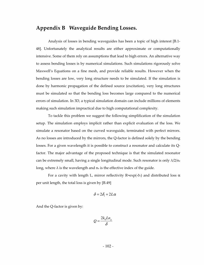
- 102 -
Appendix B Waveguide Bending Losses.
Analysis of losses in bending waveguides has been a topic of high interest [B.1-
48]. Unfortunately the analytical results are either approximate or computationally
intensive. Some of them rely on assumptions that lead to high errors. An alternative way
to assess bending losses is by numerical simulations. Such simulations rigorously solve
Maxwell’s Equations on a fine mesh, and provide reliable results. However when the
bending losses are low, very long structure needs to be simulated. If the simulation is
done by harmonic propagation of the defined source (excitation), very long structures
must be simulated so that the bending loss becomes large compared to the numerical
errors of simulation. In 3D, a typical simulation domain can include millions of elements
making such simulation impractical due to high computational complexity.
To tackle this problem we suggest the following simplification of the simulation
setup. The simulation employs implicit rather than explicit evaluation of the loss. We
simulate a resonator based on the curved waveguide, terminated with perfect mirrors.
As no losses are introduced by the mirrors, the Q-factor is defined solely by the bending
losses. For a given wavelength it is possible to construct a resonator and calculate its Q-
factor. The major advantage of the proposed technique is that the simulated resonator
can be extremely small, having a single longitudinal mode. Such resonator is only λ/2/ne
long, where λ is the wavelength and ne is the effective index of the guide.
For a cavity with length L, mirror reflectivity R=exp(-δ1) and distributed loss α
per unit length, the total loss is given by [B.49]
αδδ L22 1 +=
And the Q-factor is given by:
δ
gLnkQ
02=
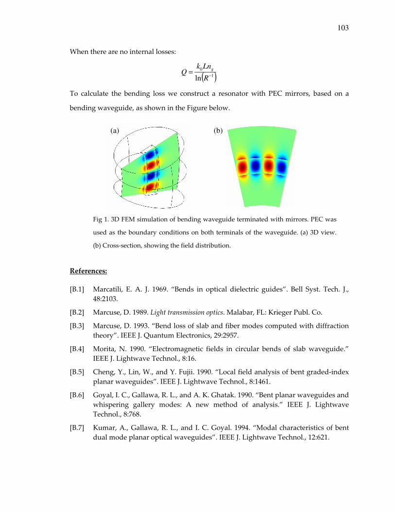
103
When there are no internal losses:
( )1
0
ln −=
R
LnkQ
g
To calculate the bending loss we construct a resonator with PEC mirrors, based on a
bending waveguide, as shown in the Figure below.
Fig 1. 3D FEM simulation of bending waveguide terminated with mirrors. PEC was
used as the boundary conditions on both terminals of the waveguide. (a) 3D view.
(b) Cross-section, showing the field distribution.
References:
[B.1] Marcatili, E. A. J. 1969. “Bends in optical dielectric guides”. Bell Syst. Tech. J., 48:2103.
[B.2] Marcuse, D. 1989. Light transmission optics. Malabar, FL: Krieger Publ. Co.
[B.3] Marcuse, D. 1993. “Bend loss of slab and fiber modes computed with diffraction theory”. IEEE J. Quantum Electronics, 29:2957.
[B.4] Morita, N. 1990. “Electromagnetic fields in circular bends of slab waveguide.” IEEE J. Lightwave Technol., 8:16.
[B.5] Cheng, Y., Lin, W., and Y. Fujii. 1990. “Local field analysis of bent graded-index planar waveguides”. IEEE J. Lightwave Technol., 8:1461.
[B.6] Goyal, I. C., Gallawa, R. L., and A. K. Ghatak. 1990. “Bent planar waveguides and whispering gallery modes: A new method of analysis.” IEEE J. Lightwave Technol., 8:768.
[B.7] Kumar, A., Gallawa, R. L., and I. C. Goyal. 1994. “Modal characteristics of bent dual mode planar optical waveguides”. IEEE J. Lightwave Technol., 12:621.
(a) (b)

104
[B.8] Renner, H. 1992. “Bending losses of coated single-mode fibers: A simple approach”. IEEE J. Lightwave Technol., 10:544.
[B.9] Wassmann, F. 1999. “Modal field analysis of circularly bent single-mode fibers”. IEEE J. Lightwave Technol., 17:957.
[B.10] Berglund, W., and A. Gopinath. 2000. “WKB analysis of bend losses in optical waveguides”. IEEE J. Lightwave Technol., 18:1161.
[B.11] Dai D. and Sheng Z., 2007. "Numerical analysis of silicon-on-insulator ridge nanowires by using a full-vectorial finite-difference method mode solver," J. Opt. Soc. Am. B 24, 2853-2859.
[B.12] Srinivasan, H., Bommalakunta, B., Chamberlain, A., Hastings, J. T. 2009. “Finite element analysis and experimental verification of SOI waveguide banding loss”, Microwave and optical tech. lett. 51, No. 3.
[B.13] Heiblum, M, Harris J., 1975. “Analysis of curved optical waveguides by conformal transformation “,IEEE J. Quantum Electronics 11, 75 – 83.
[B.14] Doerr, C.R., and Kogelnik, H. 2008. “Dielectric Waveguide Theory”, J. Light. Tech. 26 (9).
[B.15] Rowland, D. 1997. “Nonperturbative calculation of bend loss for a pulse in a bent planar waveguide”, IEE Proceedings Optoelectronics 144, 91-96.
[B.16] Kim, W.-K. and Kim, C.-M. 2002. “Radiation Losses of Bent Planar Waveguides”, Fiber and Integrated Optics 21, 219-232.
[B.17] Vlasov, Y. and McNab, S. 2004. "Losses in single-mode silicon-on-insulator strip waveguides and bends," Opt. Express 12, 1622-1631.
[B.18] Foresi, J. S., Lim, D. R., Liao, L., Agarwal, A. M., and Kimerling, L. C. 1997. “Small radius bends and large angle splitters in SOI Waveguides”, SPIE 3007.
[B.19] Bastiaansen H. J. M., van der Keur J. M. and Blok H. "Rigorous, full-vectorial source-type integral equation analysis of circularly curved channel waveguides", IEEE Trans. Microw. Theory Tech., vol. 43, pp. 401 1995.
[B.20] Bastiaansen H. J. M., Crayé H. E. and Blok H. "Source-type integral equation analysis of circularly curved channel waveguides in a multilayered background", IEEE Trans. Microw. Theory Tech., vol. 43, pp. 1597 1995.
[B.21] Kim S. and Gopinath A. "Vector analysis of optical dielectric waveguide bends using finite-difference method", J. Lightw. Techol., vol. 14, pp. 2085 1996.
[B.22] Lui W. W., Xu C.-L., Hirono T., Yokoyama K. and Huang W.-P. "Full-vectorial wave propagation in semiconductor optical bending waveguides and equivalent straight waveguide approximations", J. Lightw. Techol., vol. 16, pp. 910 1998.

105
[B.23] Feng N.-N., Zhou G.-R., Xu C. and Huang W.-P. "Computation of full-vector modes for bending waveguide using cylindrical perfectly matched layers", J. Lightw. Techol., vol. 20, pp. 1976 2002.
[B.24] Kakihara K., Kono N., Saitoh K. and Koshiba M. "Full-vectorial finite element method in a cylindrical coordinate system for loss analysis of photonic wire bends", Opt. Express, vol. 14, pp. 11128 2006.
[B.25] Pregla R. "The method of lines for the analysis of dielectric waveguide bends", J. Lightw. Techol., vol. 14, pp. 634 1996.
[B.26] Pascher W. "Modelling of rib waveguide bends for sensor applications", Opt. Quantum Electron., vol. 33, pp. 433 2001.
[B.27] Goncharenko I. A., Helfert S. F. and Pregla R. "Radiation loss and mode field distribution in curved holey fibers", Int. J. Electron. Commun., vol. 59, pp. 185 2005.
[B.28] Ritter J. and Amdt F. "Efficient FDTD/matrix-pencil method for the full-wave scattering parameter analysis of waveguiding structures", IEEE Trans. Microw. Theory Tech., vol. 44, pp. 2450 1996.
[B.29] Paul D. I., Craddock I. J. and Railton C. J. "Simple and accurate hybrid FDTD model of uniform waveguide bends", Electron. Lett., vol. 40, pp. 247 2004.
[B.30] Koning J., Rieben R. N. and Rodrigue G. H. "Vector finite-element modeling of the full-wave Maxwell equations to evaluate power loss in bent optical fibers", J. Lightw. Techol., vol. 23, pp. 4147 2005.
[B.31] Dacles-Mariani J. and Rodrigue G. H. "Study of optically induced effects due to bending and twisting using the vector finite-element method", J. Opt. Soc. Amer. B, Opt. Phys., vol. 23, pp. 1743 2006.
[B.32] Marcuse D. "Field deformation and loss caused by curvature of optical fibers", J. Opt. Soc. Amer., vol. 66, pp. 311 1976.
[B.33] Marcuse D. "Influence of curvature on the losses of doubly clad fibers", Appl. Opt., vol. 21, pp. 4208 1982.
[B.34] Trinh T. N. and Mittra R. "Field profile in a single-mode curved dielectric waveguide of rectangular cross section", IEEE Trans. Microw. Theory Tech., vol. MTT-29, pp. 1315 1981.
[B.35] Nicolet A., Zolla F. and Guenneau S."Modelling of twisted optical waveguides with edge elements", Eur. Phys. J. Appl. Phys., vol. 28, pp. 153 2004.
[B.36] Nicolet A., Movchan A. B., Guenneau S. and Zolla F."Asymptotic modelling of weakly twisted electrostatic problems", C. R. Mecanique, vol. 334, pp. 91 2006.

106
[B.37] Waldron R. A. "A helical coordinate system and its applications in electromagnetic theory", Quart. J. Mech. Appl. Math., vol. 11, pp. 438 1958.
[B.38] Post E. J., Formal Structure of Electromagnetics, pp. 1962. :North-Holland
[B.39] Klyamkin S. S. "Electromagnetic field equations for the helically symmetric systems", Electrichestvo, pp. 74 1988.
[B.40] Germano M. "On the effect of torsion on a helical pipe flow", J. Fluid Mech., vol. 125, pp. 1 1982.
[B.41] Yee K. S. "Numerical solution of initial boundary value problems involving Maxwell"s equations in isotropic media", IEEE Trans. Antennas Propag., vol. 14, pp. 302 1966.
[B.42] Gedney S. D. and Roden J. A. "Numerical stability of nonorthogonal FDTD methods", IEEE Trans. Antennas Propag., vol. 48, pp. 231 2000.
[B.43] Liu Y. "Fourier analysis of numerical algorithms for the Maxwell equations", J. Comput. Phys., vol. 124, pp. 396 1996.
[B.44] Taflove A. Advances in Computational Electrodynamics: The Finite-Difference Time-Domain Method, pp. 1998. :Artech House
[B.45] Shyroki D. M. and Lavrinenko A. V. "Perfectly matched layer method in the finite-difference time-domain and frequency-domain calculations", Phys. Stat. Sol. B, vol. 244, pp. 3506 2007.
[B.46] Shyroki D. M. "Efficient Cartesian-grid-based modeling of rotationally symmetric bodies", IEEE Trans. Microw. Theory Tech., vol. 55, pp. 1132 2007.
[B.47] Hiremath K. R., Hammer M., Stoffer R., Prkna L. "Analytic approach to dielectric optical bent slab", Opt. Quantum Electron., vol. 37, pp. 37 2005.
[B.48] Jiang Z. and Marciante J. R. "Mode-area scaling of helical-core, dual-clad fiber lasers and amplifiers using an improved bend-loss model", J. Opt. Soc. Amer. B, Opt. Phys., vol. 23, pp. 2051 2006.
[B.49] Siegman, A. E. Lasers, University Science 1986.

- 107 -
Appendix C Analysis of a Waveguide Coupled Resonator
In this summary we demonstrate how the transmission and reflection through a
waveguide side-coupled to a resonator can be obtained. The scattering matrix is
composed of elements defined in the following form:
jmaj
iij
m
a
bS
≠=
=
,0
For a 4-port device shown in Fig 1, the S-matrix is given as [Coldren 1994]:
Fig 1. Ports numbering and nomenclature used in the formalism (above); 2-port device
obtained from 4-port device by introducing the mirrors (below).
( ) ( )( ) ( )
( ) ( )( ) ( )
Lje
LLj
LLj
LjL
LjL
Sβ
κκ
κκ
κκ
κκ
−
−
−
−
−
=
0cos0sin
cos0sin0
0sin0cos
sin0cos0
For the new device shown in Fig 1 below, the scattering matrix is obtained:
a1 b1
a2 b2
a4 b4
a3 b3
a1 b1
a2 b2
r4 r3

108
=
rt
trS
Where
( )( ) Li
Li
eLrr
eLrr
22
43
22
4
cos1
sinβ
β
κ
κ−
−
−
−= ,
( )( ) Li
Li
Li
eLeLrr
errt
β
β
β
κκ
−
−
−
−
−= cos
cos1
122
43
2
43 .
When 043 rrr == and the time dependence is chosen so that the propagation direction is
Lie
β− instead of Lie
β− , we obtain the result given by Eqs 15 and 15 in Chapter III.
References:
[C.1]L.A. Coldren, S.W. Corzine, “Diode lasers and photonic integrated circuits”, 1995,
ch. 6, p. 289.
- 109 -
Appendix D Metallic Mirrors: Fabrication Recipe
Fabrication of resonator with metallic mirrors consisted of the following steps:
1. Fabrication of the waveguides (done at UC, Santa Barbara, on JEOL electron-beam
writer).
1.1. HSQ is spin coated on a wafer to produce a thickness of 130 nm, and baked.
1.2. The resist is exposed with an electron beam with the following parameters:
V=50kV, write-field 500μm × 500μm.
1.3. The resist is developed using TMAH for 2 min. and rinsed with water.
1.4. Dry-etch of Si using HSQ as a mask to define the waveguides using RIE/ICP
machine P100 from Oxford Instruments.
2. Wet-etch in diluted (1:10) solution of buffered oxide etch, BOE, (1:6), for 10 sec to
remove the residual HSQ.
3. Overlay e-beam lithography to define the mirrors.
3.1. Spin-coat PMMA 950, A9 (Microchem) at 4000 RPM for 40 sec. This produces a
thickness of 1.1μm.
3.2. Baking on a hotplate for 2 min. at 180 ºC.
3.3. Exposure to an ebeam (RAITH) with the following parameters: V=20kV,
Ip=80pA, Aperture=30μm, aperture optimization = depth, area dosage 280
μC/cm2.
3.4. Develop for 90 sec in MIBK (Microchem 1:3 with IPA), and rinsing for 30sec in
IPA.
3.5. Second dry-etch of Si using HSQ as a mask to define the openings in the
waveguides for the mirrors. Same parameters were used in this etch as in the
previous one.
3.6. Dry-etch of SiO2 using P80 from Oxford Instruments.
4. Mirror deposition with lift-off:
110
4.1. E-beam evaporation of gold (Au) at a rate of 0.4 A/s using Temescal BJD 1800
(ebeam-1), while cooling the substrate with liquid Nitrogen.
4.2. Lift-off in warm acetone for ~ 24 hrs (60 ºC on a hotplate).
5. Deposition of SiO2 with PECVD using Oxford PLasmalab for 10 min. and a
substrate temperature of 240 ºC. The leads to a film with a thickness of 730 nm
with an index ~1.44, as obtained from reflectometry.

- 111 -
Appendix E Lift-off: Fabrication Imperfections
The images below show the metal roughness introduced in the lift-off process. Also,
manifestation of shadowing effect, where e-beam evaporation of metal is shadowed by
the PMMA resist is shown in fig (e).
(b) (a)
(c)
(d) (e)

112
Appendix F Directional Coupling
Here we briefly summarize the CMT used in Section 1 of Chapter III. Following the
model of CMT [Buckman 1992], we consider a structure depicted in Fig 1. The field in
waveguide A in the absence of waveguide B is described as a linear superposition of
modes with propagation constants βm and field profiles fm(z). In a similar way, the
modes in waveguide B in the absence of waveguide A are also described by an
analogous expression. The entire structure has modes defined by the following
expression:
( ) ( ) ( )∑=m
mmm exp zjzfzEE β (1)
In the absence of waveguide A, or in the absence of waveguide B, the mode coefficients
Em are constant (no coupling). However each waveguide introduces a perturbation of
the mode of the second waveguide, causing coupling between the modes.
Fig 1. Two parallel slab waveguides. (a) Each waveguide creates a perturbation of
the modes of the second guide. (b) Refractive indices of the structure.
z
x
x
n
n1
n3 n2
n0
perturbation
(a) (b)
n1
n3
n2
n0
perturbation
A
B

113
With the perturbation, each mode has amplitude varying along the z-direction, due to
the transfer of power from one mode to another. This variation is described by the
following equation:
( )∑≠
∆=−pm
mpm exp zjEjECdz
dEmppp
p κ (2)
Where mpκ is the coefficient describing the coupling between modes m and p,
pmmp ββ −=∆ is the mismatch between the propagation constants, and pC is a measure
of how much the perturbation changes the unperturbed propagation constant pβ :
( )∫ ∆′−
= dxffj
kpm
p
mp εβ
κ2
2
0 (3)
( )∫ ∆′−
= dxffj
kC pp
p
p εβ2
2
0 (4)
Here 2n∆=∆ε is the perturbed dielectric constant. To facilitate the solution we now
modify the mode definition to:
( ) ( ) ( )zjCzAzE mmm exp= (5)
Substituting this into Eq 2 leads to:
( )∑≠
∆=pm
mpm
~exp zjA
dz
dAmp
p κ (6)
114
Where [ ]ppmmmp
~CC +−+=∆ ββ .
We will now derive the solution of Eq 6 for a directional coupler, shown in Fig 1, for two
similar waveguides (n1=n3). Assuming each waveguide is a single mode waveguide in a
given polarization we obtain:
( ) ( ) ( ) ( ) ( )
( ) ( ) ( ) ( ) ( )zEzjEzE
zjEzEzE
κκ
κκ
cos0sin0
sin0cos0
212
211
+=
+=
(7)
Having the initial conditions, ( )01E and ( )02E , the field profile can be found in each
coordinate z as ( ) ( ) ( )00 21 EEzE += .

- 115 -
Appendix G Coupling Coefficient and Supermodes
Here we show how the coupling coefficient can be obtained from FEM simulations for
an arbitrary structure and polarization. This technique allows calculation of a very low
coupling constant, that is difficult to calculate with other techniques.
Let us start with a 2D geometry, such as the one depicted in Fig 1 of Appendix G. To
calculate the coupling for TE-polarization we simulate a structure with the boundary
conditions as shown in Fig 1.
Fig 1: Calculation of coupling for TE-polarization. PEC boundary conditions are
imposed to select modes with the electric field along the x-axis. The scale bar shows
the wavelength used in the simulations. The figure shows two modes – symmetric
(a) and anti-symmetric (b).
The composite structure has at least two modes: symmetric and antisymmetric with
respect to the electric field, with the guided indices +n and −n correspondingly. The
coupling is found from the guided indices [Buckman 1992]:
( )−+ −= nnλ
πκ (1)
The coupling coefficient for TM-polarization is calculated in a similar way using PMC
boundary conditions as depicted in Fig 2.
x
y PEC
(a)
(b)
λ

116
Fig 2: Calculation of coupling for TM-polarization. PMC boundary conditions are
imposed to select modes with the electric field along the x-axis.
PMC
(a)
(b)
λ

- 117 -
Appendix H Distributed Bragg reflector (DBR).
Here we review the coupled mode theory (CMT) for the structure depicted in Fig 1
below. The perturbation is now assumed to be periodic along the propagation axis of the
form:
( ) ( ) ( )xgKznzxn cos, δ=∆ (1)
Here g(x) is the distribution of the perturbation along the x-axis, and K is the grating k-
vector K=2π/Λ. Let us now assume two modes with amplitudes E1 and E2 and
propagation constants β1 and β2.
Fig 1: Distributed Bragg reflector with period Λ.
In a way similar to CMT of the directional coupler, we obtain equations of the form:
( )
( )zjEdz
dE
zjEdz
dE
∆−=
∆=
exp
exp
1122
2211
κ
κ
(2)
x
y
Λ
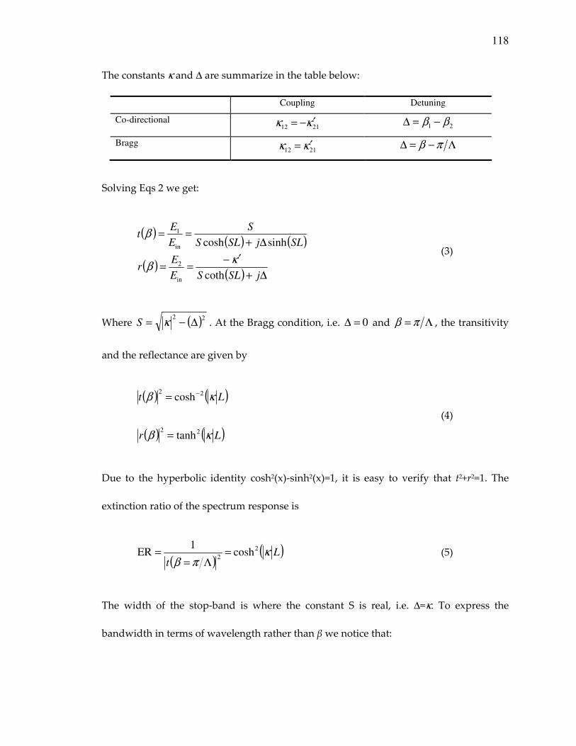
118
The constants κ and ∆ are summarize in the table below:
Coupling Detuning
Co-directional 2112 κκ ′−= 21 ββ −=∆
Bragg 2112 κκ ′= Λ−=∆ πβ
Solving Eqs 2 we get:
( )( ) ( )
( )( ) ∆+
′−==
∆+==
jSLSE
Er
SLjSLS
S
E
Et
coth
sinhcosh
in
2
in
1
κβ
β
(3)
Where ( )22∆−= κS . At the Bragg condition, i.e. 0=∆ and Λ= πβ , the transitivity
and the reflectance are given by
( ) ( )
( ) ( )Lr
Lt
κβ
κβ
22
22
tanh
cosh
=
= −
(4)
Due to the hyperbolic identity cosh2(x)-sinh2(x)=1, it is easy to verify that t2+r2=1. The
extinction ratio of the spectrum response is
( )( )L
tκ
πβ
2
2cosh
1ER =
Λ== (5)
The width of the stop-band is where the constant S is real, i.e. ∆=κ. To express the
bandwidth in terms of wavelength rather than β we notice that:

119
gnk
λλ
β 0−=∂
∂ (6)
From here the bandwidth is easily obtained:
gnk
λκβ
λ
βλ
0
1
=∆
∂
∂=∆
−
(7)
Here k0=2π/λ. So as a reference, for a stopband width of ∆λ=1nm at the wavelength of
λ=1500nm and assuming a group index of ng=3 the required coupling coefficient is
κ=81cm-1.

- 120 -
Appendix I Label-Free Biochemical Sensing
The idea behind label-free biochemical sensing is depicted in Fig 1. An optical
waveguide exhibits an effective index neff that varies as molecules bind to the surface of
the waveguide.
Fig 1. The concept of label-free biochemical sensing: (a) receptors are immobilized
onto an optical waveguide, (b) analyte is delivered to the structure and molecules
(proteins) bind to the receptors, (c) dielectric layer with an effective thickness h and
index np is formed on the surface, (d) grating is used to excite the optical mode. (e)
Reflection spectrum is measured over time, and the amount of shift in the resonant
wavelength is quantified. (f) The temporal dependence of the shift upon introduction
of the analyte and rinse.
(a) (b) (c) (d)
λ
λ
λ
time
R
∆λ
(e)
time
Introduction
of the
analyte
Rinse
∆λ
(f)
Shift due to the
binding of
proteins to the
receptors

121
The reflection spectrum exhibits dips that correspond to excitations of the guided waves
[Petit 1980, Rosenblatt 1997]. These dips happen when one of the diffraction orders of
the grating matches the propagation constant of the waveguide. As molecules bind to
the surface, they perturb the optical mode of the waveguide and cause shifts in the
resonances. By monitoring these shifts the amount of perturbation and therefore the
amount of molecules that bound to the waveguide can be quantified.
Fig 2. Three structures used for biochemical sensing: Metal-dielectric interface (a),
dielectric waveguide (b), and Fabry-Perot resonator.
We will now compare three structures shown in Fig 2 – surface plasmon,
dielectric waveguide, and a resonator. It should be noticed here that the comparison is
not straightforward for the following reason. The structure depicted in Fig 2c is a
resonator with eigenmodes defined in time (temporal frequencies, ω). The structures in
Fig 2a and 2b are waveguides, with their eigenmodes defined in space (spatial
frequencies or the k-vectors, β). To facilitate the comparison between the two types of
structures we will assume Kretschmann configuration, where the modes are excited
using a grating designed for normal incidence. In this case the amount of shift in the
(a) (b) (c)
Substrate Waveguide Analyte Metal Proteins
x
z
n1
n2
np
εm
n1 np

122
wavelength can be quantified for the structures depicted in Figs 2a and 2b, and that shift
can be compared to the shift in the structure shown in Fig 2c.
Surface Sensitivity Refs
( ) 02
dm
2
d
2/3
2
dm
m
p
eff 2hk
n
n
nn
n
+′−
+′
′=
∂
∂
εε
ε
Homola
Surface
Plasmons
( ) 0
m
4
spp12
p
2
1eff k
nnnn
h
n
ε ′−−=
∂
∂ −−
Lukocz
Slab
Waveguide ( ) ( )( ) ( )
ρ
−+
−+
−
−
−=
∂
∂
1
12
2eff
2
1eff
2
peff
2
1eff
2
1
2
2
2
1
2
p
effeff
2
eff
2
Feff
nnnn
nnnn
nn
nn
nd
nn
h
n
Tiefenthaler
Parameters Definitions
h thickness of the adsorbed layer
np index of the adsorbed layer
neff effective index
n1 top (liquid) cladding index
n2 index of the core (slab) waveguide
nd index of the dielectric (liquid) cladding on top of the metal
deff effective width of the mode (core + decay lengths into claddings)
ρ 1 (for TM modes), 0 (for TE)
ε`m real part of the dielectric constant of metal
If grating coupler is used to excite the guided mode of the waveguide or the surface
plasmon (Kretschmann configuration) at normal incidence, the period of the grating, Λ,
must satisfy:
Λ=
π2eff0nk (1)

123
Or in other words effnΛ=λ . From here the wavelength sensitivity to adsorption of
molecules can be obtained by derivation with respect to the thickness of the adlayer h:
eff
effeff
nh
n
h
n
h
λλ
∂
∂=Λ
∂
∂=
∂
∂ (2)
To calculate the wavelength sensitivity to adsorption of molecules for dielectric
waveguide or surface plasmon based device in Kretschmann configuration we substitute
the value of hn ∂∂ eff , from the table above into Eq 2.
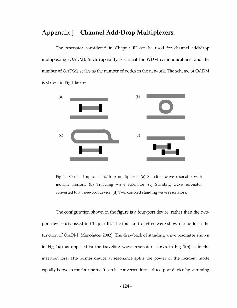
- 124 -
Appendix J Channel Add-Drop Multiplexers.
The resonator considered in Chapter III can be used for channel add/drop
multiplexing (OADM). Such capability is crucial for WDM communications, and the
number of OADMs scales as the number of nodes in the network. The scheme of OADM
is shown in Fig 1 below.
Fig 1. Resonant optical add/drop multiplexer. (a) Standing wave resonator with
metallic mirrors. (b) Traveling wave resonator. (c) Standing wave resonator
converted to a three-port device. (d) Two coupled standing wave resonators.
The configuration shown in the figure is a four-port device, rather than the two-
port device discussed in Chapter III. The four-port devices were shown to perform the
function of OADM [Manolatou 2002]. The drawback of standing wave resonator shown
in Fig 1(a) as opposed to the traveling wave resonator shown in Fig 1(b) is in the
insertion loss. The former device at resonance splits the power of the incident mode
equally between the four ports. It can be converted into a three-port device by summing
(a) (b)
(d) (c)

125
two of the ports, as shown in Fig 1(c), leading to 3dB loss at multiplexing. To overcome
this difficulty, two identical coupled resonators can be used in a configuration shown in
Fig 1(d). Such configuration leads to splitting of the resonance into two – symmetric and
anti-symmetric standing wave resonances, resulting in a lower insertion loss [Manolatou
2002]. More intriguing combinations of resonators can be investigated to construct high-
order filters. Such filters offer higher extinction ratio between adjacent communication
channels and higher out-of-band roll-off. These configurations require further
investigation.
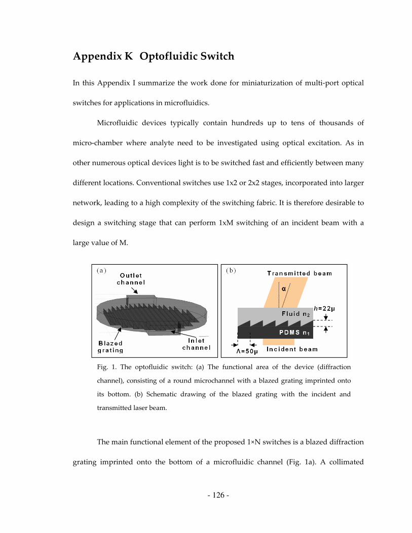
- 126 -
Appendix K Optofluidic Switch
In this Appendix I summarize the work done for miniaturization of multi-port optical
switches for applications in microfluidics.
Microfluidic devices typically contain hundreds up to tens of thousands of
micro-chamber where analyte need to be investigated using optical excitation. As in
other numerous optical devices light is to be switched fast and efficiently between many
different locations. Conventional switches use 1x2 or 2x2 stages, incorporated into larger
network, leading to a high complexity of the switching fabric. It is therefore desirable to
design a switching stage that can perform 1xM switching of an incident beam with a
large value of M.
Fig. 1. The optofluidic switch: (a) The functional area of the device (diffraction
channel), consisting of a round microchannel with a blazed grating imprinted onto
its bottom. (b) Schematic drawing of the blazed grating with the incident and
transmitted laser beam.
The main functional element of the proposed 1×N switches is a blazed diffraction
grating imprinted onto the bottom of a microfluidic channel (Fig. 1a). A collimated

127
monochromatic beam of light incident onto the grating is deflected by an angle
proportional to the mismatch between the refractive indices of the material of the
grating and the liquid in the channel (Fig. 1b). For a given wavelength of light,
diffraction maxima occur at a discrete set of refractive indices of the liquid that
correspond to a discrete set of beam deflection angles, making a 1×N optical switch.
Within each period (segment) of an ideal thin blazed grating, the phase of an
incident monochromatic wave is linearly modulated along the direction perpendicular
to the grooves of the grating (Fig. 1). The slope of this linear modulation is proportional
to the difference between the refractive indices of the material of the grating and the
medium on top of the grating, 1n and 2n . A diffraction maximum occurs, when the
optical path difference over one period of the blazed profile is equal to an integer
number of wavelengths:
( ) mhnn λ=− 21 (1)
where h is the height of the grating profile, λ is the wavelength of the incident light in
vacuum, and m is an integer indicating the order of diffraction. When the condition of a
diffraction maximum is met, a normally incident plane wave is coherently deflected by
an angle mα found from the equation
( ) ( ) Λ−=Λ= //sin 21 hnnmm λα (2)
128
where Λ is the period of the grating. At a diffraction maximum, an ideal blazed grating
acts as a prism with an angle ( )Λ− /tan 1h .
Fig. 2. Optofluidic switch: (a) Layout of microchannels in the device: the flow layer
(black and red) with four inlets (in0 – in3), two vents (v1 and v2), and one outlet; and
the control layer (blue) with 5 inlets (c0 – c4). The blazed grating is schematically
shown as a patterned area. (b) A photograph of an actual microfluidic PDMS chip
bonded to a cover glass.
The switch has a response time of 55 ms, insertion loss of 2.1 dB, cross-talk of 10
dB, and extinction ratio of 10 dB. The theoretical extinction ratio is higher than 20 dB and
can be achieved by mitigation of fabrication imperfections in the replication process of
the gratings. Further details on the design, fabrication, and characterization can be found
in reference [Groisman 2008].
The proposed 1xN optofluidic switches have an advantage of potentially simple
integration with other microfluidic elements for lab-on-a-chip application. Furthermore,
the cross-talk and the extinction ratio in the present 1x4 switch are expected to be
substantially improved by perfecting the shape of the diffraction grating, and the
response time of the switch can be reduced by modifying the microfluidic channels.

129
Cascading of multiple switches can lead to a switch with a large count of ports and
reduced complexity.
A. Groisman, S. Zamek, K. Campbell, L. Pang, U. Levy, and Y. Fainman, "Optofluidic 1x4 Switch," Opt. Express 16, 13499-13508 (2008).

- 130 -
Appendix L Affinity Sensors – Surface Coverage.
Optical label-free affinity sensors measure variations in a parameter such as
wavelength or angle at which a resonance is observed. In these sensors the following
assumptions are made: np is the refractive index of the adlayer (adsorbed proteins), nc is
the one of the cladding (assay), and h is the thickness of the adlayer. The resonance shifts
are calculated from these parameters. Correspondence between these and the surface
coverage Γ in terms of mass/(surface area) is known [de-Feijter 1978]:
hdcdn
nn cp −=Γ
Here c is the concentration of the protein in the adlayer in units of mass/volume, and
dcdn is the variation of the effective refractive index of the adlayer with the
concentration c. For most assays buffer solution with nc=1.33 is used. From numerous
investigations of the properties of bound proteins [Langmuir 1939, de-Feijter 1978, Ball
1998] it is known that dcdn is on the order of 0.2 ml/g and thicknesses are 1÷100 nm,
and the refractive index of protein is np~1.46. For thin adlayer, where the equation above
holds, we obtain Γ~0.65[g/cm3] *h.
On the other hand sensitivity hS ∂∂≡ λλ is known for a given optical structure
(see Section 0 III). We can now derive the sensitivity versus mass coverage:
λ
λλS
g
cm
dh
d
dh
d
d
dS
≈
Γ=
Γ≡
− 31
5.1

131
For a given device the sensitivity λS is known and the detection limit of the measurand,
∆λ, is defined by the setup. Then the detection limit in terms of mass coverage can also
be obtained:
S
λ∆=∆Γ
For the device shown in Section 0 III-2, the S~1.5*Sλ=1.5*0.5~0.75[cm3/g]. For the detection
limit of 50 pm, we obtained ∆Γ~6.6[ng/cm2]. The total area of the device is
A=40μm×200μm=8e-5[cm2], therefore the minimum detectable mass of bound protein is
∆Γ*A=0.5 pico-gram.
1. De Feijter J.A., Benjamins J., Veer F.A., Biopolymers 17, pp. 1759-1772, 1978
2. Langmuir I., Schaefer V.J., “Properties and Structure of Protein Monolayers”,
Chemical Reviews 24 (2), pp. 181-202 (1939)
3. Ball V., Ramsden J.J., “Buffer dependence of refractive index increments of protein
solutions”, Biopolymers 46, 7, 1998, pp. 489-492