
Mini
68
AUTOMATIC STREET LIGHT CONTROL USING LDR Abstract: This project aims at designing and executing the advanced development in embedded systems for energy saving of street lights with light depending resistor. Nowadays, human has become too busy and he is unable to find time even to switch the lights wherever not necessary. This can be seen more effectively in the case of street lights. The present system is like, the street lights will be switched on in the evening before the sun sets and they are switched off the next day morning after there is sufficient light on the roads. But the actual timings for these street lights to be switched on are when there is absolute darkness. With this, the power will be wasted up to some extent. This project gives the best solution for electrical power wastage. Also the manual operation of the lighting system is completely eliminated. In our project we are using LDR, which varies according to the amount of light falling on its surface, this give an indication for us whether it is a day/night time. We have placed IR sensors in both sides of the road, which can be controlled by Micro controller (AT89C51).The IR‘s will be
-
Upload
vinay-kataria -
Category
Documents
-
view
386 -
download
5
Transcript of Mini
AUTOMATIC STREET LIGHT CONTROL USING LDR
Abstract:
This project aims at designing and executing the advanced development in
embedded systems for energy saving of street lights with light depending resistor.
Nowadays, human has become too busy and he is unable to find time even to switch the
lights wherever not necessary. This can be seen more effectively in the case of street
lights. The present system is like, the street lights will be switched on in the evening
before the sun sets and they are switched off the next day morning after there is sufficient
light on the roads. But the actual timings for these street lights to be switched on are
when there is absolute darkness. With this, the power will be wasted up to some extent.
This project gives the best solution for electrical power wastage. Also the manual
operation of the lighting system is completely eliminated.
In our project we are using LDR, which varies according to the amount of light falling on
its surface, this give an indication for us whether it is a day/night time. We have placed
IR sensors in both sides of the road, which can be controlled by Micro controller
(AT89C51).The IR‘s will be activated only on the night time. If any obstacle crosses the
IR, automatically particular light will be ON, for few seconds.
In our project we use regulated 5V, 500mA power supply. 7805 three terminal voltage
regulator is used for voltage regulation. Bridge type full wave rectifier is used to rectify
the ac out put of secondary of 230/12V step down transformer.
The programming language used for developing the software to the microcontroller is
Embedded/Assembly. The KEIL cross compiler is used to edit, compile and debug this
program. Here in our application we are using AT89C51 microcontroller which is Flash
Programmable IC.AT represents the Atmel Corporation ‘C’ represents CMOS technology
is used for designing the IC. We believe that our idea provides better than the existing
system.
In the present project street lights are taken into consideration where the
above discussed factors are rectified in them. This is achieved with the help of an
embedded system. By using this as the basic principle we can design centralized
intelligent system for the perfect usage of streetlights in any place (Viz Village, Town)
can be developed.
INDEX
1. INTRODUCTION…………………………………………………
Embedded Systems
Objective Of The Project
Block Diagram
Block Diagram Description
2. DESCRIPTION OF THE PROJECT…………………………..
Circuit Diagram
Circuit Description
3. HARDWARE DESCRIPTION………………………………….
Micro controller
LDR
IR
Power Supply
4. SOFTWARE DESCRIPTION
Flow Chart
Program
5. CONCLUSION
6. FUTURE ENHANCEMENT
7. BIBLIOGRAPHY
EMBEDDED SYSTEMS:
Embedded systems are designed to do some specific task, rather than be a
general-purpose computer for multiple tasks. Some also have real time performance
constraints that must be met, for reason such as safety and usability; others may have low
or no performance requirements, allowing the system hardware to be simplified to reduce
costs.
An embedded system is not always a separate block - very often it is
physically built-in to the device it is controlling. The software written for embedded
systems is often called firmware, and is stored in read-only memory or flash convector
chips rather than a disk drive. It often runs with limited computer hardware resources:
small or no keyboard, screen, and little memory.
Wireless communication has become an important feature for commercial
products and a popular research topic within the last ten years. There are now more
mobile phone subscriptions than wired-line subscriptions. Lately, one area of commercial
interest has been low-cost, low-power, and short-distance wireless communication used
for \personal wireless networks." Technology advancements are providing smaller and
more cost effective devices for integrating computational processing, wireless
communication, and a host of other functionalities. These embedded communications
devices will be integrated into applications ranging from homeland security to industry
automation and monitoring. They will also enable custom tailored engineering solutions,
creating a revolutionary way of disseminating and processing information. With new
technologies and devices come new business activities, and the need for employees in
these technological areas. Engineers who have knowledge of embedded systems and
wireless communications will be in high demand. Unfortunately, there are few adorable
environments available for development and classroom use, so students often do not learn
about these technologies during hands-on lab exercises. The communication mediums
were twisted pair, optical fiber, infrared, and generally wireless radio.
Objective of the project:-
The main consideration in the present field technologies are Automation,
Power consumption and cost effectiveness. Automation is intended to reduce man power
with the help of intelligent systems. Power saving is the main consideration forever as the
source of the power(Thermal, Hydro etc.,)are getting diminished due to various reasons.
The main aim of the project is Automatic street power saving system with LDR, this is to
save the power. We want to save power automatically instead of doing manual. So its
easy to make cost effectiveness. This saved power can be used in some other cases. So in
villages, towns etc we can design intelligent systems for the usage of street lights.

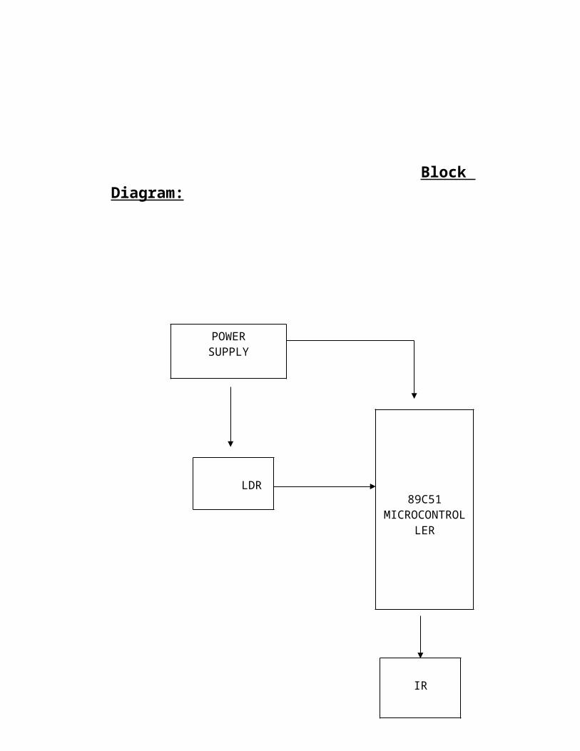
Block Diagram:
LDR89C51
MICROCONTROLLER
IR
POWERSUPPLY
Block Diagram Explanation: .
In this project, we are going to switch off the street lights
automatically as the day starts. The duration of the day differs from season to season,
accordingly our module works based upon the light intensity so as to when to start or
stop. For this we are using Light Dependent Resistor (LDR) as the light sensor, which
communicates with the required information to the micro controller.
Here we are using micro controller, LDR, and relay. By using the LDR we
can operate the lights, i.e when the light is available then it will be in the OFF state and
when it is dark then the light will be in ON state, it means LDR is inversely proportional
to light. When the light falls on the LDR it sends the commands to the micro controller
that it should be in the OFF state then it switch off’s the light, all these commands are
sent to the controller then according to that the devices operate. We use a relay to act as
an ON OFF switch, the load is connected to these relays.
HARDWARE DESCRIPTION
The block diagram of the system is as shown in the fig. The system basically consists of a
1. Micro controller,2. LDR3. IR4. Power supply,
MICROCONTROLLER ARCHITECHTURE
Microprocessor has following instructions to perform:
1. Reading instructions or data from program memory ROM.
2. Interpreting the instruction and executing it.
3. Microprocessor Program is a collection of instructions stored in a
Nonvolatile memory.
4. Read Data from I/O device
5. Process the input read, as per the instructions read in program memory.
6. Read or write data to Data memory.
7. Write data to I/O device and output the result of processing to O/P device.
NECESSITY OF MICROCONTROLLERS:
Microprocessors brought the concept of programmable devices and made
many applications of intelligent equipment. Most applications, which do not need large
amount of data and program memory, tended to be:
Costly:
The microprocessor system had to satisfy the data and program requirements
so, sufficient RAM and ROM are used to satisfy most applications .The peripheral
control equipment also had to be satisfied. Therefore, almost all-peripheral chips were
used in the design. Because of these additional peripherals cost will be comparatively
high.
An example:
8085 chip needs:
An Address latch for separating address from multiplex address and data.32-
KB RAM and 32-KB ROM to be able to satisfy most applications. As also Timer /
Counter, Parallel programmable port, Serial port, Interrupt controller are needed for its
efficient applications.
In comparison a typical Micro controller 8051 chip has all that the 8051 board has
except a reduced memory as follows.
4K bytes of ROM as compared to 32-KB, 128 Bytes of RAM as compared to 32-KB.
Bulky:
On comparing a board full of chips (Microprocessors) with one chip with all
components in it (Micro controller).
Debugging:
Lots of Microprocessor circuitry and program to debug. In Micro controller there
is no Microprocessor circuitry to debug.
Slower Development time: As we have observed Microprocessors need a lot of
debugging at board level and at program level, where as, Micro controller do not have the
excessive circuitry and the built-in peripheral chips are easier to program for operation.
So peripheral devices like Timer/Counter, Parallel programmable port, Serial
Communication Port, Interrupt controller and so on, which were most often used were
integrated with the Microprocessor to present the Micro controller .RAM and ROM also
were integrated in the same chip. The ROM size was anything from 256 bytes to 32Kb or
more. RAM was optimized to minimum of 64 bytes to 256 bytes or more.
Typical Micro controller have all the following features:
8/16/32 CPU
Instruction set rich in I/O & bit operations.
One or more I/O ports.
One or more timer/counters.
One or more interrupt inputs and an interrupt controller
One or more serial communication ports.
Analog to Digital /Digital to Analog converter
One or more PWM output
Network controlled interface
Why AT 89C51? :
The system requirements and control specifications clearly rule out the use of 16,
32 or 64 bit micro controllers or microprocessors. Systems using these may be earlier to
implement due to large number of internal features. They are also faster and more reliable
but, the above application is satisfactorily served by 8-bit micro controller. Using an
inexpensive 8-bit Micro controller will doom the 32-bit product failure in any
competitive market place.
Coming to the question of why to use AT89C51 of all the 8-bit Micro controller
available in the market the main answer would be because it has 4 Kb on chip flash
memory which is just sufficient for our application. The on-chip Flash ROM allows the
program memory to be reprogrammed in system or by conventional non-volatile memory
Programmer. Moreover ATMEL is the leader in
Flash technology in today’s market place and hence using AT 89C51 is the optimal
solution.
8051 micro controller architecture:
The 8051 architecture consists of these specific features:
Eight –bit CPU with registers A (the accumulator) and B
Sixteen-bit program counter (PC) and data pointer (DPTR)
Eight- bit stack pointer (PSW)
Eight-bit stack pointer (Sp)
Internal ROM or EPROM (8751) of 0(8031) to 4K (8051)
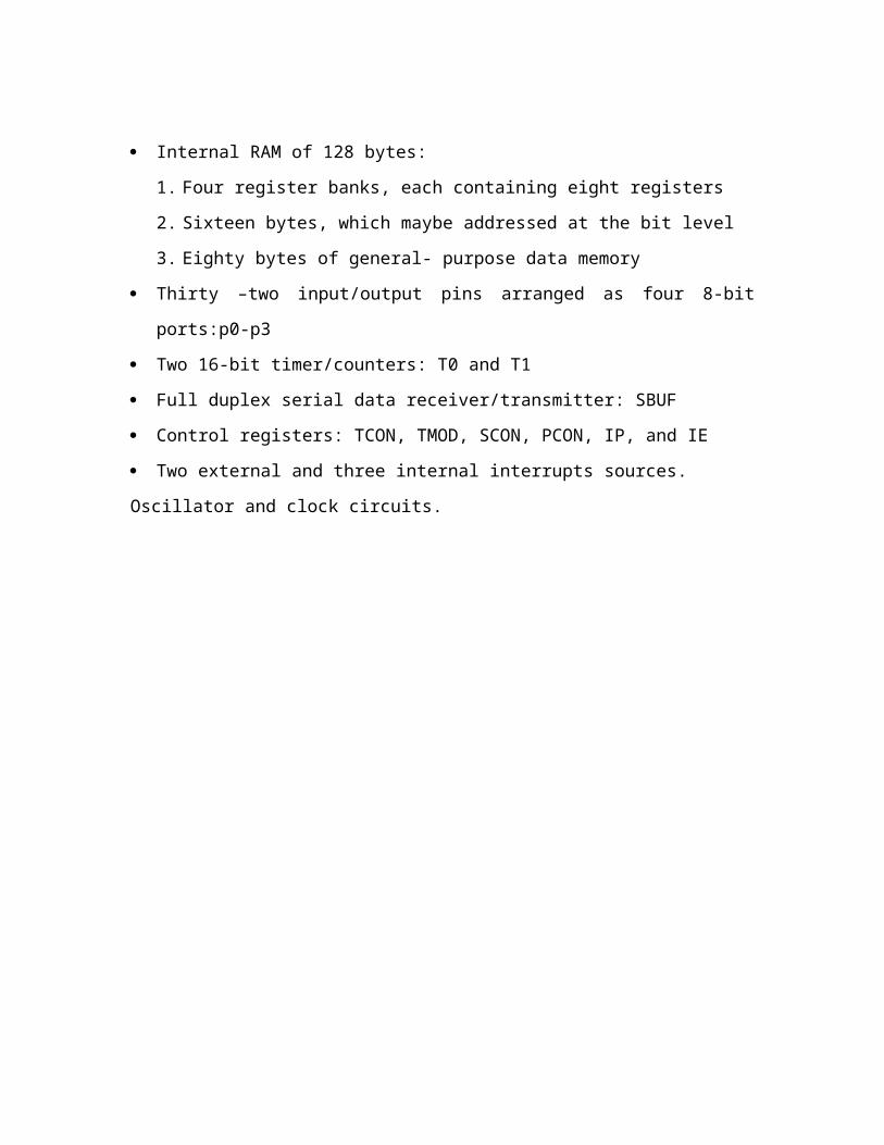
Internal RAM of 128 bytes:
1. Four register banks, each containing eight registers
2. Sixteen bytes, which maybe addressed at the bit level
3. Eighty bytes of general- purpose data memory
Thirty –two input/output pins arranged as four 8-bit ports:p0-p3
Two 16-bit timer/counters: T0 and T1
Full duplex serial data receiver/transmitter: SBUF
Control registers: TCON, TMOD, SCON, PCON, IP, and IE
Two external and three internal interrupts sources.
Oscillator and clock circuits.
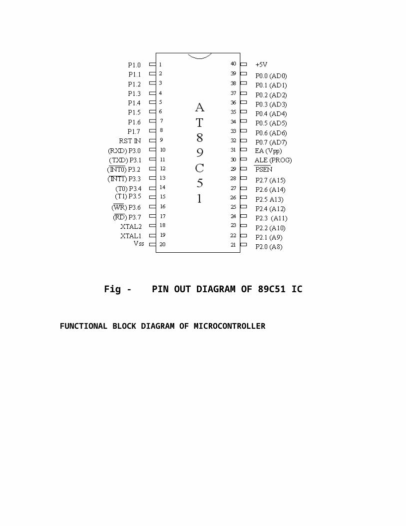
Fig - PIN OUT DIAGRAM OF 89C51 IC
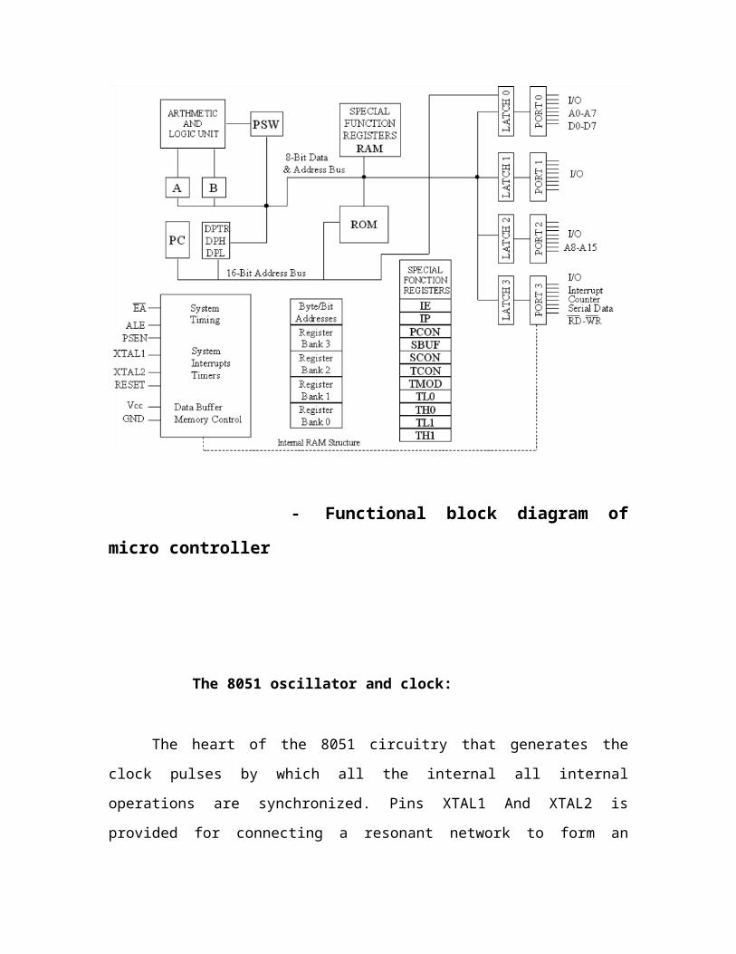
FUNCTIONAL BLOCK DIAGRAM OF MICROCONTROLLER
- Functional block diagram of micro controller
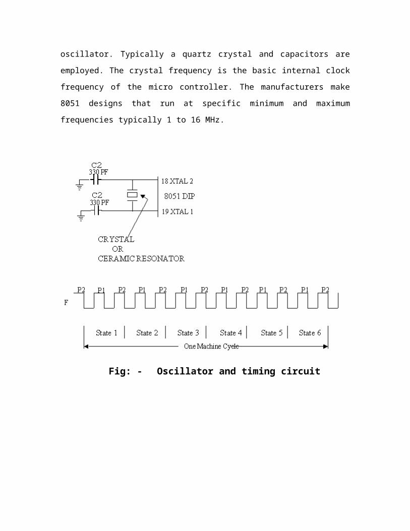
The 8051 oscillator and clock:
The heart of the 8051 circuitry that generates the clock pulses by which all the
internal all internal operations are synchronized. Pins XTAL1 And XTAL2 is provided
for connecting a resonant network to form an oscillator. Typically a quartz crystal and
capacitors are employed. The crystal frequency is the basic internal clock frequency of
the micro controller. The manufacturers make 8051 designs that run at specific minimum
and maximum frequencies typically 1 to 16 MHz.
Fig: - Oscillator and timing circuit
Types of memory:
The 8051 have three general types of memory. They are on-chip memory,
external Code memory and external Ram. On-Chip memory refers to physically existing
memory on the micro controller itself. External code memory is the code memory that
resides off chip. This is often in the form of an external EPROM. External RAM is the
Ram that resides off chip. This often is in the form of standard static RAM or flash
RAM.
a) Code memory
Code memory is the memory that holds the actual 8051 programs that is to be run.
This memory is limited to 64K. Code memory may be found on-chip or off-chip. It is
possible to have 4K of code memory on-chip and 60K off chip memory simultaneously.
If only off-chip memory is available then there can be 64K of off chip ROM. This is
controlled by pin provided as EA
b) Internal RAM
The 8051 have a bank of 128 bytes of internal RAM. The internal RAM is found
on-chip. So it is the fastest Ram available. And also it is most flexible in terms of reading
and writing. Internal Ram is volatile, so when 8051 is reset, this memory is cleared. 128
bytes of internal memory are subdivided. The first 32 bytes are divided into 4 register
banks. Each bank contains 8 registers. Internal RAM also contains 128 bits, which are
addressed from 20h to 2Fh. These bits are bit addressed i.e. each individual bit of a byte
can be addressed by the user. They are numbered 00h to 7Fh. The user may make use of
these variables with commands such as SETB and CLR.
Special Function registered memory:
Special function registers are the areas of memory that control specific
functionality of the 8051 micro controller.
a) Accumulator (0E0h)
As its name suggests, it is used to accumulate the results of large no of
instructions. It can hold 8 bit values.
B) B register (0F0h)
The B register is very similar to accumulator. It may hold 8-bit value. The b
register is only used by MUL AB and DIV AB instructions. In MUL AB the higher byte
of the product gets stored in B register. In div AB the quotient gets stored in B with the
remainder in A.
c) Stack pointer (81h)
The stack pointer holds 8-bit value. This is used to indicate where the next value
to be removed from the stack should be taken from. When a value is to be pushed onto
the stack, the 8051 first store the value of SP and then store the value at the resulting
memory location. When a value is to be popped from the stack, the 8051 returns the
value from the memory location indicated by SP and then decrements the value of SP.
d) Data pointer
The SFRs DPL and DPH work together work together to represent a 16-bit value
called the data pointer. The data pointer is used in operations regarding external RAM
and some instructions code memory. It is a 16-bit SFR and also an addressable SFR.
e) Program counter
The program counter is a 16 bit register, which contains the 2 byte address, which
tells the 8051 where the next instruction to execute to be found in memory. When the
8051 is initialized PC starts at 0000h. And is incremented each time an instruction is
executes. It is not addressable SFR.
f) PCON (power control, 87h)
The power control SFR is used to control the 8051’s power control modes.
Certain operation modes of the 8051 allow the 8051 to go into a type of “sleep mode ”
which consume much lee power.
g) TCON (timer control, 88h)
The timer control SFR is used to configure and modify the way in which the
8051’s two timers operate. This SFR controls whether each of the two timers is running
or stopped and contains a flag to indicate that each timer has overflowed. Additionally,
some non-timer related bits are located in TCON SFR. These bits are used to configure
the way in which the external interrupt flags are activated, which are set when an
external interrupt occurs.
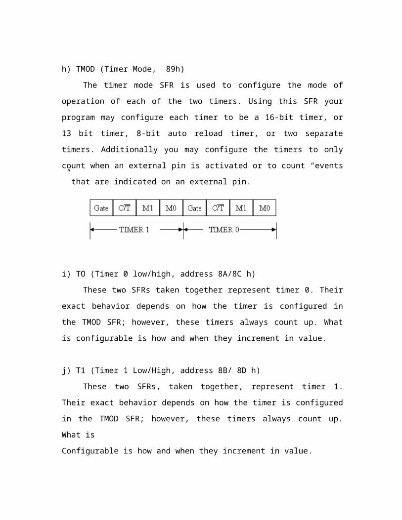
h) TMOD (Timer Mode, 89h)
The timer mode SFR is used to configure the mode of operation of each of the
two timers. Using this SFR your program may configure each timer to be a 16-bit timer,
or 13 bit timer, 8-bit auto reload timer, or two separate timers. Additionally you may
configure the timers to only count when an external pin is activated or to count “events ”
that are indicated on an external pin.
i) TO (Timer 0 low/high, address 8A/8C h)
These two SFRs taken together represent timer 0. Their exact behavior depends
on how the timer is configured in the TMOD SFR; however, these timers always count
up. What is configurable is how and when they increment in value.
j) T1 (Timer 1 Low/High, address 8B/ 8D h)
These two SFRs, taken together, represent timer 1. Their exact behavior depends
on how the timer is configured in the TMOD SFR; however, these timers always count
up. What is
Configurable is how and when they increment in value.
k) P0 (Port 0, address 90h, bit addressable)
This is port 0 latch. Each bit of this SFR corresponds to one of the pins on a micro
controller. Any data to be outputted to port 0 is first written on P0 register. For e.g., bit 0
of port 0 is pin P0.0, bit 7 is pin p0.7. Writing a value of 1 to a bit of this SFR will send a
high level on the corresponding I/O pin whereas a value of 0 will bring it to low level.
l) P1 (port 1, address 90h, bit addressable)
This is port latch1. Each bit of this SFR corresponds to one of the pins on a
micro controller. Any data to be outputted to port 0 is first written on P0 register. For
e.g., bit 0 of port 0 is pin P1.0, bit 7 is pin P1.7. Writing a value of 1 to a bit of this SFR
will send a high level on the corresponding I/O pin whereas a value of 0 will bring it to
low level
m) P2 (port 2, address 0A0h, bit addressable) :
This is a port latch2. Each bit of this SFR corresponds to one of the pins on a
micro controller. Any data to be outputted to port 0 is first written on P0 register. For e.g.,
bit 0 of port 0 is pin P2.0, bit 7 is pin P2.7. Writing a value of 1 to a bit of this SFR will
send a high level on the corresponding I/O pin whereas a value of 0 will bring it to low
level.
n) P3(port 3,address B0h, bit addressable) :
This is a port latch3. Each bit of this SFR corresponds to one of the pins on a
micro controller. Any data to be outputted to port 0 is first written on P0 register. For e.g.,
bit 0 of port 0 is pin P3.0, bit 7 is pin P3.7. Writing a value of 1 to a bit of this SFR will
send a high level on the corresponding I/O pin whereas a value of 0 will bring it to low
level
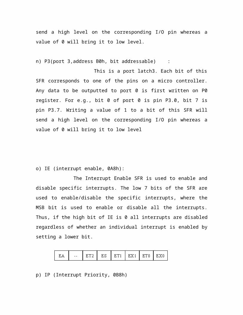
o) IE (interrupt enable, 0A8h):
The Interrupt Enable SFR is used to enable and disable specific interrupts. The
low 7 bits of the SFR are used to enable/disable the specific interrupts, where the MSB
bit is used to enable or disable all the interrupts. Thus, if the high bit of IE is 0 all
interrupts are disabled regardless of whether an individual interrupt is enabled by setting
a lower bit.
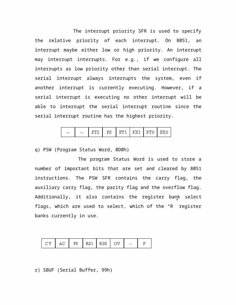
p) IP (Interrupt Priority, 0B8h)
The interrupt priority SFR is used to specify the relative priority of each interrupt.
On 8051, an interrupt maybe either low or high priority. An interrupt may interrupt
interrupts. For e.g., if we configure all interrupts as low priority other than serial
interrupt. The serial interrupt always interrupts the system, even if another interrupt is
currently executing. However, if a serial interrupt is executing no other interrupt will be
able to interrupt the serial interrupt routine since the serial interrupt routine has the
highest priority.
q) PSW (Program Status Word, 0D0h)
The program Status Word is used to store a number of important bits that are set
and cleared by 8051 instructions. The PSW SFR contains the carry flag, the auxiliary
carry flag, the parity flag and the overflow flag. Additionally, it also contains the register
bank select flags, which are used to select, which of the “R” register banks currently in
use.
r) SBUF (Serial Buffer, 99h)
SBUF is used to hold data in serial communication. It is physically two registers.
One is writing only and is used to hold data to be transmitted out of 8051 via TXD. The
other is read only and holds received data from external sources via RXD. Both mutually
exclusive registers use address 99h.
I/O ports:
One major feature of a microcontroller is the versatility built into the input/output
(I/O) circuits that connect the 8051 to the outside world. The main constraint that limits
numerous functions is the number of pins available in the 8051 circuit. The DIP had 40
pins and the success of the design depends on the flexibility incorporated into use of
these pins. For this reason, 24 of the pins may each used for one of the two entirely
different functions which depend, first, on what is physically connected to it and, then, on
what software programs are used to “program” the pins.

PORT 0
Port 0 pins may serve as inputs, outputs, or, when used together, as a bi directional
low-order address and data bus for external memory. To configure a pin as input, 1 must
be written into the corresponding port 0 latch by the program. When used for interfacing
with the external memory, the lower byte of address is first sent via PORT0, latched
using Address latch enable (ALE) pulse and then the bus is turned around to become the
data bus for external memory.
PORT 1
Port 1 is exclusively used for input/output operations. PORT 1 pins have no dual
function. When a pin is to be configured as input, 1 is to be written into the
corresponding Port 1 latch.
PORT 2
Port 2 maybe used as an input/output port. It may also be used to supply a high –
order address byte in conjunction with Port 0 low-order byte to address external memory.
Port 2 pins are momentarily changed by the address control signals when supplying the
high byte a 16-bit address. Port 2 latches remain stable when external memory is
addressed, as they do not have to be turned around (set to 1) for data input as in the case
for Port 0.
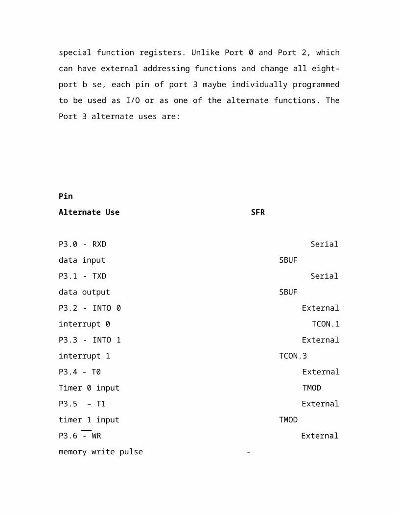
PORT 3
Port 3 may be used to input /output port. The input and output functions can be
programmed under the control of the P3 latches or under the control of various special
function registers. Unlike Port 0 and Port 2, which can have external addressing functions
and change all eight-port b se, each pin of port 3 maybe individually programmed to be
used as I/O or as one of the alternate functions. The Port 3 alternate uses are:
Pin Alternate Use SFR
P3.0 - RXD Serial data input SBUF
P3.1 - TXD Serial data output SBUF
P3.2 - INTO 0 External interrupt 0 TCON.1
P3.3 - INTO 1 External interrupt 1 TCON.3
P3.4 - T0 External Timer 0 input TMOD
P3.5 – T1 External timer 1 input TMOD
P3.6 - WR External memory write pulse -
P3.7 - RD External memory read pulse -
INTERRUPTS:
Interrupts are hardware signals that are used to determine conditions that exist in
external and internal circuits. Any interrupt can cause the 8051 to perform a hardware
call to an interrupt –handling subroutine that is located at a predetermined absolute
address in the program memory.
Five interrupts are provided in the 8051. Three of these are generated automatically
by the internal operations: Timer flag 0, Timer Flag 1, and the serial port interrupt (RI or
TI) Two interrupts are triggered by external signals provided by the circuitry that is
connected to the pins INTO 0 and INTO1. The interrupts maybe enable or disabled, given
priority or otherwise controlled by altering the bits in the Interrupt Enabled (IE) register,
Interrupt Priority (IP) register, and the Timer Control (TCON) register. . These interrupts
are mask able i.e. they can be disabled. Reset is a non maskable interrupt which has the
highest priority. It is generated when a high is applied to the reset pin. Upon reset, the
registers are loaded with the default values.
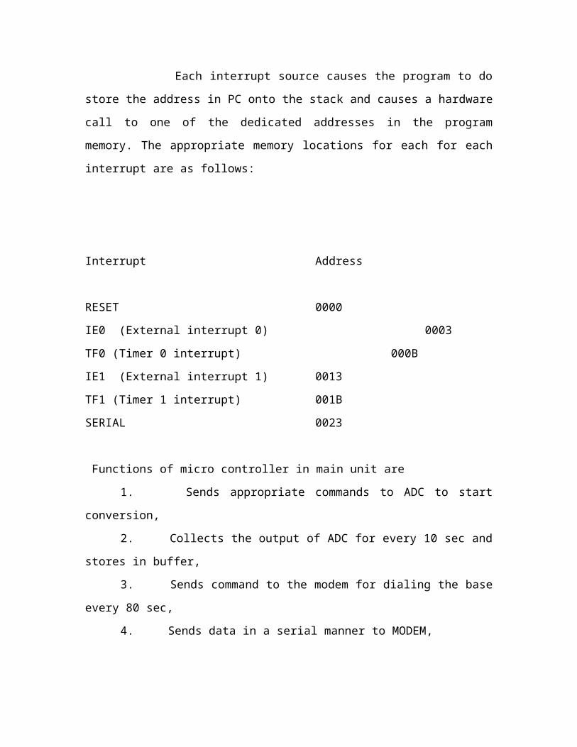
Each interrupt source causes the program to do store the address in PC onto the
stack and causes a hardware call to one of the dedicated addresses in the program
memory. The appropriate memory locations for each for each interrupt are as follows:
Interrupt Address
RESET 0000
IE0 (External interrupt 0) 0003
TF0 (Timer 0 interrupt) 000B
IE1 (External interrupt 1) 0013
TF1 (Timer 1 interrupt) 001B
SERIAL 0023
Functions of micro controller in main unit are
1. Sends appropriate commands to ADC to start conversion,
2. Collects the output of ADC for every 10 sec and stores in buffer,
3. Sends command to the modem for dialing the base every 80 sec,
4. Sends data in a serial manner to MODEM,
5. After data gets transmitted sends command for disconnection.
6. Sends appropriate information to the display unit as per status
of the communication medium.
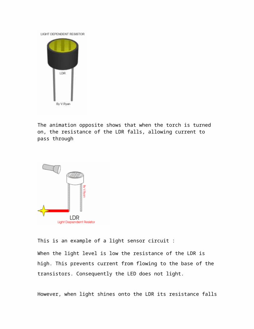
LDR
LDRs or Light Dependent Resistors are very useful especially in
light/dark sensor circuits. Normally the resistance of an LDR is very high, sometimes as
high as 1000 000 ohms, but when they are illuminated with light resistance drops
dramatically.
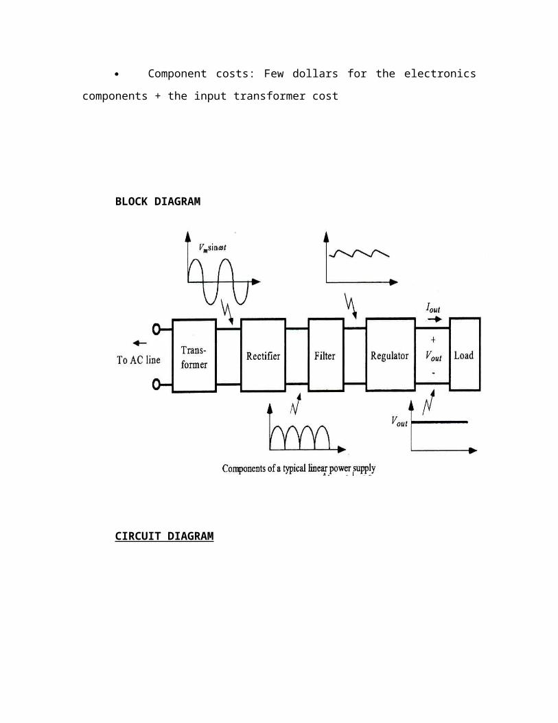
The animation opposite shows that when the torch is turned on, the resistance of the LDR falls, allowing current to pass through
This is an example of a light sensor circuit :
When the light level is low the resistance of the LDR is high. This prevents current from
flowing to the base of the transistors. Consequently the LED does not light.
However, when light shines onto the LDR its resistance falls and current flows into the
base of the first transistor and then the second transistor. The LED lights.

The preset resistor can be turned up or down to increase or decrease resistance, in this
way it can make the circuit more or less sensitive.
REGULATED POWER SUPPLY
DESCRIPTION
A variable regulated power supply, also called a variable bench power
supply, is one where you can continuously adjust the output voltage to your requirements.
Varying the output of the power supply is the recommended way to test a project after
having double checked parts placement against circuit drawings and the parts placement
guide. This type of regulation is ideal for having a simple variable bench power supply.
Actually this is quite important because one of the first projects a hobbyist should
undertake is the construction of a variable regulated power supply. While a dedicated
supply is quite handy e.g. 5V or 12V, it's much handier to have a variable supply on
hand, especially for testing. Most digital logic circuits and processors need a 5 volt power
supply. To use these parts we need to build a regulated 5 volt source. Usually you start
with an unregulated power supply ranging from 9 volts to 24 volts DC (A 12 volt power
supply is included with the Beginner Kit and the Microcontroller Beginner Kit.). To
make a 5 volt power supply, we use a LM7805 voltage regulator IC .
The LM7805 is simple to use. You simply connect the positive lead of your
unregulated DC power supply (anything from 9VDC to 24VDC) to the Input pin, connect
the negative lead to the Common pin and then when you turn on the power, you get a 5
volt supply from the Output pin.
CIRCUIT FEATURES
Brief description of operation: Gives out well regulated +5V output, output
current capability of 100 mA
Circuit protection: Built-in overheating protection shuts down output when
regulator IC gets too hot
Circuit complexity: Very simple and easy to build
Circuit performance: Very stable +5V output voltage, reliable operation
Availability of components: Easy to get, uses only very common basic
components
Design testing: Based on datasheet example circuit, I have used this circuit
successfully as part of many electronics projects
Applications: Part of electronics devices, small laboratory power supply
Power supply voltage: Unregulated DC 8-18V power supply
Power supply current: Needed output current + 5 mA
Component costs: Few dollars for the electronics components + the input
transformer cost
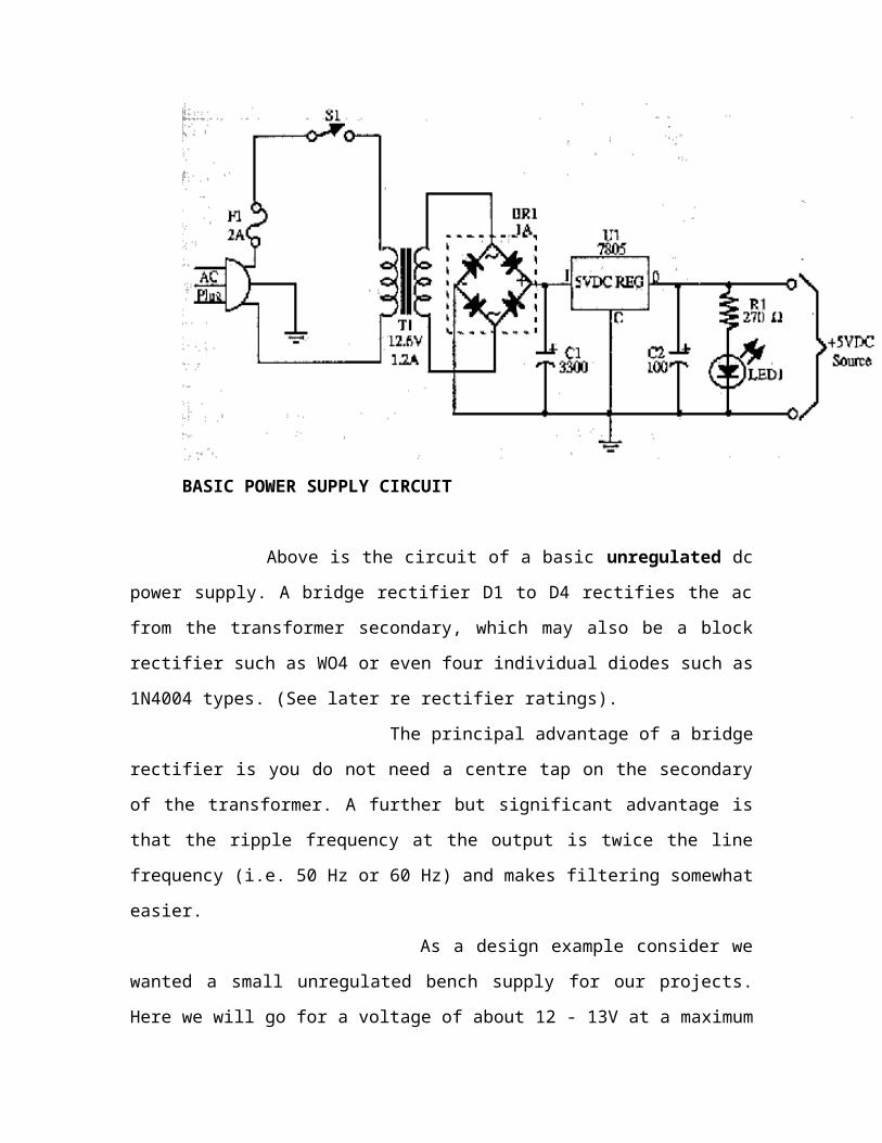
BLOCK DIAGRAM
CIRCUIT DIAGRAM
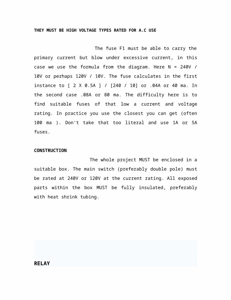
BASIC POWER SUPPLY CIRCUIT
Above is the circuit of a basic unregulated dc power supply. A bridge rectifier
D1 to D4 rectifies the ac from the transformer secondary, which may also be a block
rectifier such as WO4 or even four individual diodes such as 1N4004 types. (See later re
rectifier ratings).
The principal advantage of a bridge rectifier is you do not need a
centre tap on the secondary of the transformer. A further but significant advantage is that
the ripple frequency at the output is twice the line frequency (i.e. 50 Hz or 60 Hz) and
makes filtering somewhat easier.
As a design example consider we wanted a small unregulated bench
supply for our projects. Here we will go for a voltage of about 12 - 13V at a maximum
output current (IL) of 500ma (0.5A). Maximum ripple will be 2.5% and load regulation is
5%.
Now the RMS secondary voltage (primary is whatever is consistent
with your area) for our power transformer T1 must be our desired output Vo PLUS the
voltage drops across D2 and D4 ( 2 * 0.7V) divided by 1.414.
This means that Vsec = [13V + 1.4V] / 1.414 which equals about 10.2V. Depending on
the VA rating of your transformer, the secondary voltage will vary considerably in
accordance with the applied load. The secondary voltage on a transformer advertised as
say 20VA will be much greater if the secondary is only lightly loaded.
If we accept the 2.5% ripple as adequate for our purposes then at 13V this
becomes 13 * 0.025 = 0.325 Vrms. The peak to peak value is 2.828 times this value. Vrip
= 0.325V X 2.828 = 0.92 V and this value is required to calculate the value of C1. Also
required for this calculation is the time interval for charging pulses. If you are on a 60Hz
system it it 1/ (2 * 60 ) = 0.008333 which is 8.33 milliseconds. For a 50Hz system it is
0.01 sec or 10 milliseconds.
Remember the tolerance of the type of capacitor used here is very loose. The
important thing to be aware of is the voltage rating should be at least 13V X 1.414 or
18.33. Here you would use at least the standard 25V or higher (absolutely not 16V).With
our rectifier diodes or bridge they should have a PIV rating of 2.828 times the Vsec or at
least 29V. Don't search for this rating because it doesn't exist. Use the next highest
standard or even higher. The current rating should be at least twice the load current
maximum i.e. 2 X 0.5A or 1A. A good type to use would be 1N4004, 1N4006 or 1N4008
types.
These are rated 1 Amp at 400PIV, 600PIV and 1000PIV respectively. Always
be on the lookout for the higher voltage ones when they are on special.
TRANSFORMER RATING –
In our example above we were taking 0.5A out of the Vsec of 10V. The VA
required is 10 X 0.5A = 5VA. This is a small PCB mount transformer available in
Australia and probably elsewhere.
This would be an absolute minimum and if you anticipated drawing the
maximum current all the time then go to a higher VA rating.
The two capacitors in the primary side are small value types and if you don't
know precisely and I mean precisely what you are doing then OMIT them. Their loss
won't cause you heartache or terrible problems.
THEY MUST BE HIGH VOLTAGE TYPES RATED FOR A.C USE
The fuse F1 must be able to carry the primary current but blow under
excessive current, in this case we use the formula from the diagram. Here N = 240V /
10V or perhaps 120V / 10V. The fuse calculates in the first instance to [ 2 X 0.5A ] / [240
/ 10] or .04A or 40 ma. In the second case .08A or 80 ma. The difficulty here is to find
suitable fuses of that low a current and voltage rating. In practice you use the closest you
can get (often 100 ma ). Don't take that too literal and use 1A or 5A fuses.
CONSTRUCTION
The whole project MUST be enclosed in a suitable box. The main switch
(preferably double pole) must be rated at 240V or 120V at the current rating. All exposed
parts within the box MUST be fully insulated, preferably with heat shrink tubing.
RELAY
Description
A relay is an electrical switch that opens and closes under the control of another
electrical circuit. In the original form, the switch is operated by an electromagnet to open
or close one or many sets of contacts. It was invented by Joseph Henry in 1835. Because
a relay is able to control an output circuit of higher power than the input circuit, it can be
considered to be, in a broad sense, a form of an electrical amplifier.
Operation
When a current flows through the coil, the resulting magnetic field attracts an armature
that is mechanically linked to a moving contact. The movement either makes or breaks a
connection with a fixed contact. When the current to the coil is switched off, the armature
is returned by a force approximately half as strong as the magnetic force to its relaxed
position. Usually this is a spring, but gravity is also used commonly in industrial motor
starters. Most relays are manufactured to operate quickly. In a low voltage application,
this is to reduce noise. In a high voltage or high current application, this is to reduce
arcing.
If the coil is energized with DC, a diode is frequently installed across the coil, to dissipate
the energy from the collapsing magnetic field at deactivation, which would otherwise
generate a spike of voltage and might cause damage to circuit components. Some
automotive relays already include that diode inside the relay case. Alternatively a contact
protection network, consisting of a capacitor and resistor in series, may absorb the surge.
If the coil is designed to be energized with AC, a small copper ring can be crimped to the
end of the solenoid. This "shading ring" creates a small out-of-phase current, which
increases the minimum pull on the armature during the AC cycle.
By analogy with the functions of the original electromagnetic device, a solid-state relay is
made with a thyristor or other solid-state switching device. To achieve electrical isolation
an opto coupler can be used which is a light-emitting diode (LED) coupled with a photo
transistor.
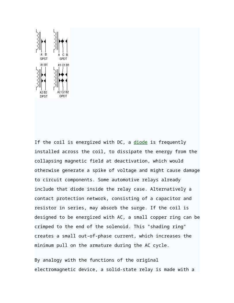
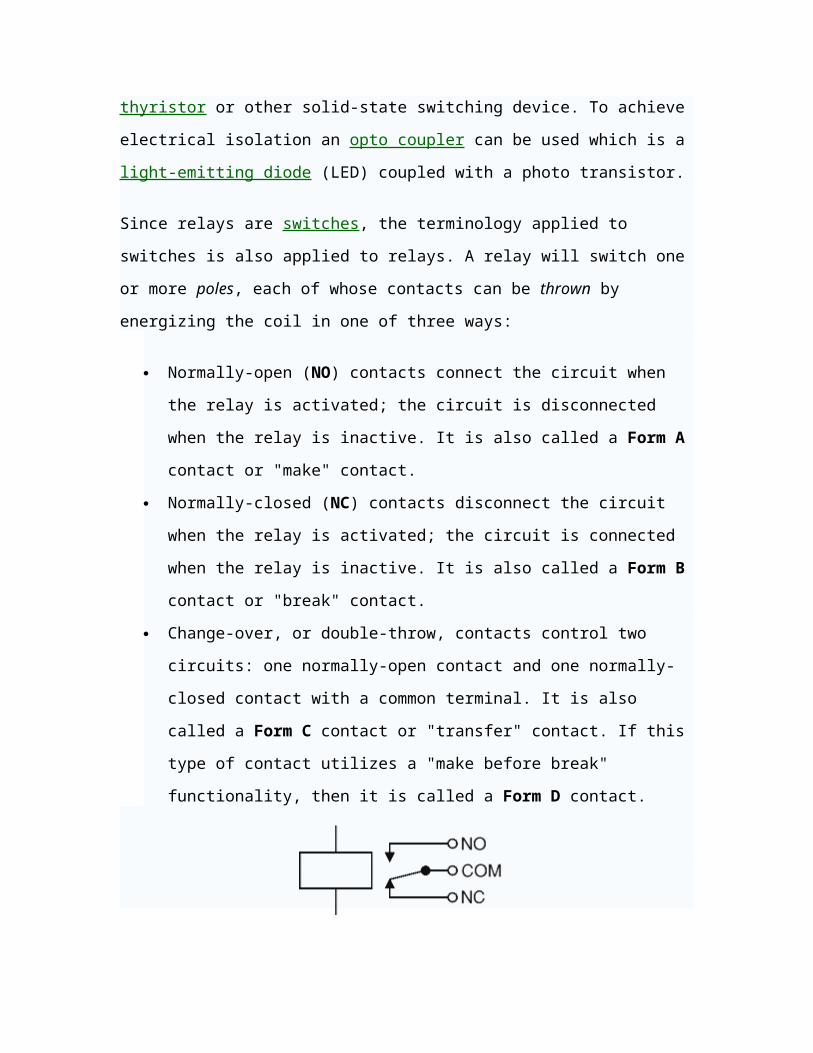
Since relays are switches, the terminology applied to switches is also applied to relays. A
relay will switch one or more poles, each of whose contacts can be thrown by energizing
the coil in one of three ways:
Normally-open (NO) contacts connect the circuit when the relay is activated; the
circuit is disconnected when the relay is inactive. It is also called a Form A
contact or "make" contact.
Normally-closed (NC) contacts disconnect the circuit when the relay is activated;
the circuit is connected when the relay is inactive. It is also called a Form B
contact or "break" contact.
Change-over, or double-throw, contacts control two circuits: one normally-open
contact and one normally-closed contact with a common terminal. It is also called
a Form C contact or "transfer" contact. If this type of contact utilizes a "make
before break" functionality, then it is called a Form D contact.
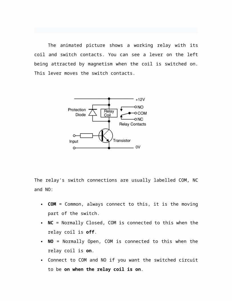
The animated picture shows a working relay with its coil and switch contacts.
You can see a lever on the left being attracted by magnetism when the coil is switched
on. This lever moves the switch contacts.
The relay's switch connections are usually labelled COM, NC and NO:
COM = Common, always connect to this, it is the moving part of the switch.
NC = Normally Closed, COM is connected to this when the relay coil is off.
NO = Normally Open, COM is connected to this when the relay coil is on.
Connect to COM and NO if you want the switched circuit to be on when the
relay coil is on.
Connect to COM and NC if you want the switched circuit to be on when the
relay coil is off.
.
SOFTWARE :
ABOUT SOFTWARE
Software’s used are:
*Keil software for c programming
*Express PCB for lay out design
*Express SCH for schematic design
What's New in µVision3?
µVision3 adds many new features to the Editor like Text Templates, Quick Function
Navigation, and Syntax Coloring with brace high lighting Configuration Wizard for
dialog based startup and debugger setup. µVision3 is fully compatible to µVision2 and
can be used in parallel with µVision2.
What is µVision3?
µVision3 is an IDE (Integrated Development Environment) that helps you write, compile,
and debug embedded programs. It encapsulates the following components:
A project manager.
A make facility.
Tool configuration.
Editor.
A powerful debugger.
To help you get started, several example programs (located in the \C51\Examples, \
C251\Examples, \C166\Examples, and \ARM\...\Examples) are provided.
HELLO is a simple program that prints the string "Hello World" using the Serial
Interface.
MEASURE is a data acquisition system for analog and digital systems.
TRAFFIC is a traffic light controller with the RTX Tiny operating system.
SIEVE is the SIEVE Benchmark.

DHRY is the Dhrystone Benchmark.
WHETS is the Single-Precision Whetstone Benchmark.
Additional example programs not listed here are provided for each device architecture.
Building an Application in µVision2
To build (compile, assemble, and link) an application in µVision2, you must:
1. Select Project -(forexample,166\EXAMPLES\HELLO\HELLO.UV2).
2. Select Project - Rebuild all target files or Build target.
µVision2 compiles, assembles, and links the files in your project.
Creating Your Own Application in µVision2
To create a new project in µVision2, you must:
1. Select Project - New Project.
2. Select a directory and enter the name of the project file.
3. Select Project - Select Device and select an 8051, 251, or C16x/ST10 device from
the Device Database™.
4. Create source files to add to the project.
5. Select Project - Targets, Groups, Files. Add/Files, select Source Group1, and add
the source files to the project.
6. Select Project - Options and set the tool options. Note when you select the target
device from the Device Database™ all special options are set automatically. You
typically only need to configure the memory map of your target hardware. Default
memory model settings are optimal for most applications.
7. Select Project - Rebuild all target files or Build target.
Debugging an Application in µVision2
To debug an application created using µVision2, you must:
1. Select Debug - Start/Stop Debug Session.
2. Use the Step toolbar buttons to single-step through your program. You may enter
G, main in the Output Window to execute to the main C function.
3. Open the Serial Window using the Serial #1 button on the toolbar.
Debug your program using standard options like Step, Go, Break, and so on.

Starting µVision2 and Creating a Project
µVision2 is a standard Windows application and started by clicking on the program icon.
To create a new project file select from the µVision2 menu
Project – New Project…. This opens a standard Windows dialog that asks you
for the new project file name.
We suggest that you use a separate folder for each project. You can simply use
the icon Create New Folder in this dialog to get a new empty folder. Then
select this folder and enter the file name for the new project, i.e. Project1.
µVision2 creates a new project file with the name PROJECT1.UV2 which contains
a default target and file group name. You can see these names in the Project
Window – Files.
Now use from the menu Project – Select Device for Target and select a CPU
for your project. The Select Device dialog box shows the µVision2 device
database. Just select the microcontroller you use. We are using for our examples the
Philips 80C51RD+ CPU. This selection sets necessary tool
options for the 80C51RD+ device and simplifies in this way the tool Configuration
Building Projects and Creating a HEX Files
Typical, the tool settings under Options – Target are all you need to start a new
application. You may translate all source files and line the application with a
click on the Build Target toolbar icon. When you build an application with
syntax errors, µVision2 will display errors and warning messages in the Output
Window – Build page. A double click on a message line opens the source file
on the correct location in a µVision2 editor window.
Once you have successfully generated your application you can start debugging.
After you have tested your application, it is required to create an Intel HEX file to
download the software into an EPROM programmer or simulator. µVision2 creates HEX
files with each build process when Create HEX files under Options for Target – Output is
enabled. You may start your PROM programming utility after the make process when
you specify the program under the option Run User Program #1.
CPU Simulation

µVision2 simulates up to 16 Mbytes of memory from which areas can be
mapped for read, write, or code execution access. The µVision2 simulator traps
and reports illegal memory accesses.
In addition to memory mapping, the simulator also provides support for the
integrated peripherals of the various 8051 derivatives. The on-chip peripherals
of the CPU you have selected are configured from the Device
Database selection
you have made when you create your project target. Refer to page 58 for more
Information about selecting a device. You may select and display the on-chip peripheral
components using the Debug menu. You can also change the aspects of each peripheral
using the controls in the dialog boxes.
Start Debugging
You start the debug mode of µVision2 with the Debug – Start/Stop Debug
Session command. Depending on the Options for Target – Debug
Configuration, µVision2 will load the application program and run the startup
code µVision2 saves the editor screen layout and restores the screen layout of the last
debug session. If the program execution stops, µVision2 opens an
editor window with the source text or shows CPU instructions in the disassembly
window. The next executable statement is marked with a yellow arrow. During
debugging, most editor features are still available.
For example, you can use the find command or correct program errors. Program source
text of your application is shown in the same windows. The µVision2 debug mode differs
from the edit mode in the following aspects:
_ The “Debug Menu and Debug Commands” described on page 28 are
Available. The additional debug windows are discussed in the following.
_ The project structure or tool parameters cannot be modified. All build
Commands are disabled.
Disassembly Window
The Disassembly window shows your target program as mixed source and assembly
program or just assembly code. A trace history of previously executed instructions may
be displayed with Debug – View Trace Records. To enable the trace history, set Debug –
Enable/Disable Trace Recording.
If you select the Disassembly Window as the active window all program step commands
work on CPU instruction level rather than program source lines. You can select a text line
and set or modify code breakpoints using toolbar buttons or the context menu commands.
You may use the dialog Debug – Inline Assembly… to modify the CPU
instructions. That allows you to correct mistakes or to make temporary changes to the
target program you are debugging.
SOURCE CODE
1. Click on the Keil uVision Icon on Desktop
2. The following fig will appear
3. Click on the Project menu from the title bar
4. Then Click on New Project

5. Save the Project by typing suitable project name with no extension in u r own folder sited in either C:\ or D:\
6. Then Click on Save button above.
7. Select the component for u r project. i.e. Atmel……
8. Click on the + Symbol beside of Atmel

9. Select AT89C51 as shown below
10. Then Click on “OK”
11. The Following fig will appear
12. Then Click either YES or NO………mostly “NO”
13. Now your project is ready to USE
14. Now double click on the Target1, you would get another option “Source
group 1” as shown in next page.
15. Click on the file option from menu bar and select “new”

16. The next screen will be as shown in next page, and just maximize it by double
clicking on its blue boarder.
17. Now start writing program in either in “C” or “ASM”
18. For a program written in Assembly, then save it with extension “. asm” and
for “C” based program save it with extension “ .C”
19. Now right click on Source group 1 and click on “Add files to Group Source”
20. Now you will get another window, on which by default “C” files will appear.
21. Now select as per your file extension given while saving the file
22. Click only one time on option “ADD”
23. Now Press function key F7 to compile. Any error will appear if so happen.
24. If the file contains no error, then press Control+F5 simultaneously.
25. The new window is as follows
26. Then Click “OK”
27. Now Click on the Peripherals from menu bar, and check your required port as
shown in fig below
28. Drag the port a side and click in the program file.
29. Now keep Pressing function key “F11” slowly and observe.
30. You are running your program successfully
FUTURE ENHANCEMENT
Wireless is the buzz of communication industry today. The
field of wireless communication is growing leaps and bounds day by day. There have
been many advancements taking place in the semiconductor industry leading to more and
more advancements in wireless technology.
The main aim of the project is to save the power, by using effectively we can save more
power, as we know that there is shortage of power nowadays in every where mostly in
villages etc. So to overcome that we can provide street lights automatically with the
centralized intelligent systems. So in future we can design many more advanced
technologies to save power.
CONCLUSION
The project “AUTOMATIC STREET LIGHT CONTROL SYSTEM
WITH LDR” has been successfully designed and tested.
Here we are saving lot of power without any wastage, by these advanced
technologies we can design many more systems which can be done by solar lights and
through these solar lights we have a vast usage at the same time we can do automatic
systems instead of doing it manually like with ldr’s.
Secondly, using highly advanced IC’s and with the help of growing
technology the project has been successfully implemented.
BIBLIOGRAPHY
The 8051 Micro controller and Embedded Systems
-Muhammad Ali Mazidi
Janice Gillispie Mazidi
The 8051 Micro controller Architecture, Programming & Applications
-Kenneth J.Ayala
Fundamentals Of Micro processors and Micro computers
-B.Ram
Micro processor Architecture, Programming & Applications
-Ramesh S.Gaonkar
Electronic Components
-D.V.Prasad
Wireless Communications

- Theodore S. Rappaport
Mobile Tele Communications
- William C.Y. Lee
References on the Web:
www.national.com
www.atmel.com
www.microsoftsearch.com
www.geocities.com