Millimeter Wave Photonics: Design, Integration and...
101
Department of Electrical and Computer Engineering Millimeter Wave Photonics: Design, Integration and Application Dennis Prather, Professor
Transcript of Millimeter Wave Photonics: Design, Integration and...
Department of Electrical and Computer Engineering
Millimeter Wave Photonics: Design, Integration and Application
Dennis Prather, Professor

Outline
• Overview of RF imaging
• Optical phase modulators
• Ultra-wideband frequency synthesis
• RF photonic module integration
• Silicon Nanomembranes for 3D RF signal
routing
• Summary

RF Imaging
RADAR
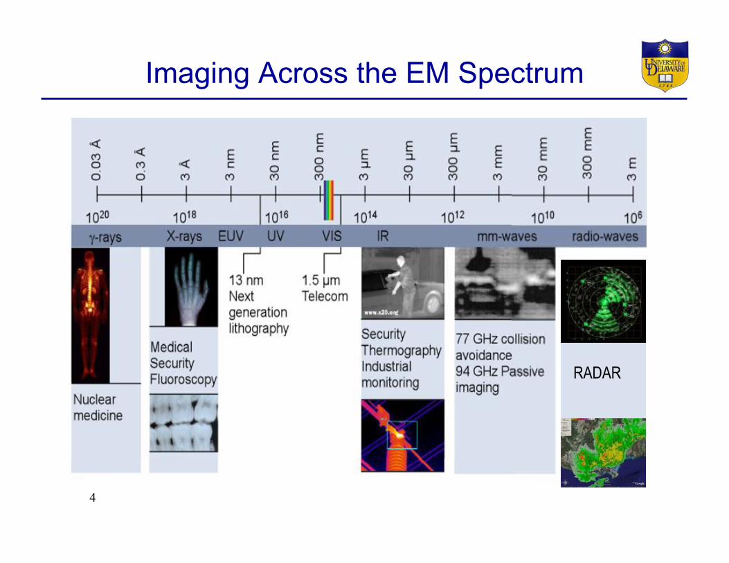
Imaging Across the EM Spectrum
4
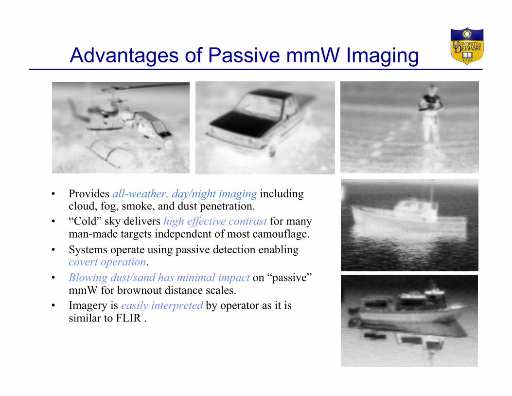
Advantages of Passive mmW Imaging
• Provides all-weather, day/night imaging including cloud, fog, smoke, and dust penetration.
• “Cold” sky delivers high effective contrast for many man-made targets independent of most camouflage.
• Systems operate using passive detection enabling covert operation.
• Blowing dust/sand has minimal impact on “passive” mmW for brownout distance scales.
• Imagery is easily interpreted by operator as it is similar to FLIR .
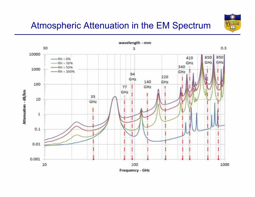
Atmospheric Attenuation in the EM Spectrum
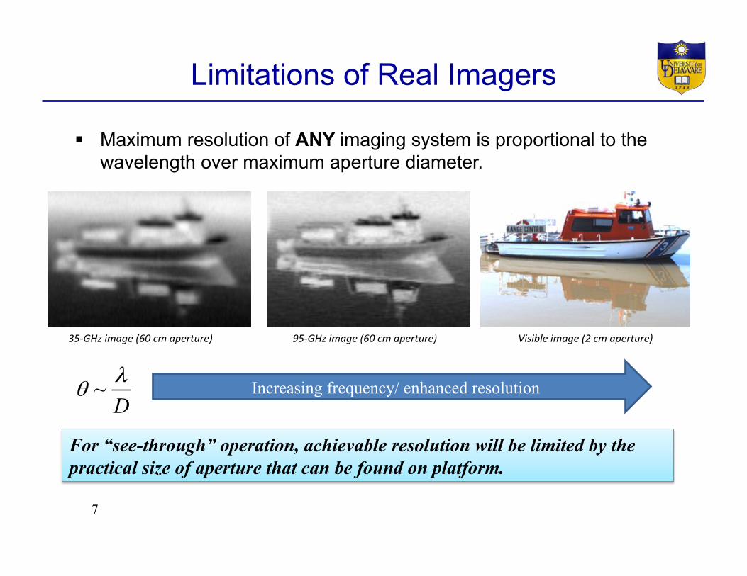
Limitations of Real Imagers
7
! Maximum resolution of ANY imaging system is proportional to the wavelength over maximum aperture diameter.
~Dλ
θ
For “see-through” operation, achievable resolution will be limited by the practical size of aperture that can be found on platform.
Increasing frequency/ enhanced resolution
Visible'image'(2'cm'aperture)'955GHz'image'(60'cm'aperture)'355GHz'image'(60'cm'aperture)'
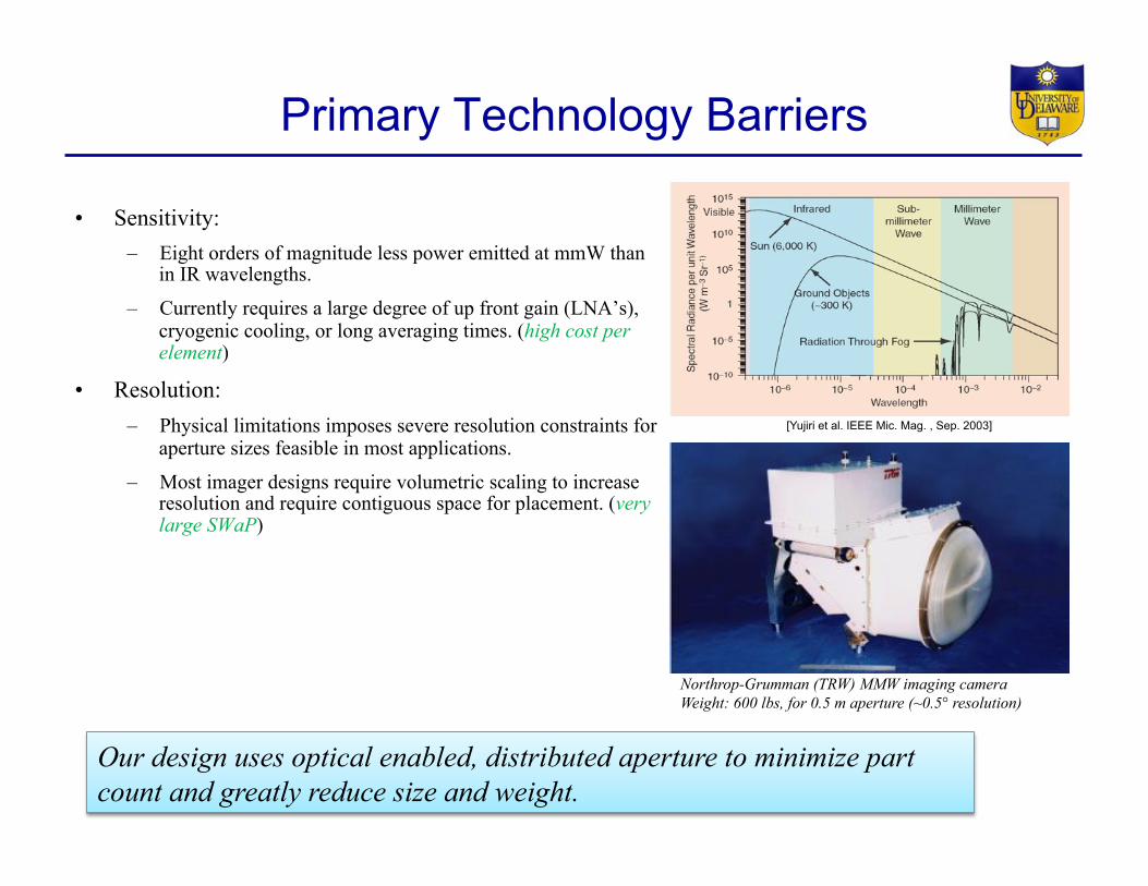
Primary Technology Barriers
• Sensitivity: – Eight orders of magnitude less power emitted at mmW than
in IR wavelengths.
– Currently requires a large degree of up front gain (LNA’s), cryogenic cooling, or long averaging times. (high cost per element)
• Resolution: – Physical limitations imposes severe resolution constraints for
aperture sizes feasible in most applications.
– Most imager designs require volumetric scaling to increase resolution and require contiguous space for placement. (very large SWaP)
8
Northrop-Grumman (TRW) MMW imaging camera Weight: 600 lbs, for 0.5 m aperture (~0.5° resolution)
Our design uses optical enabled, distributed aperture to minimize part count and greatly reduce size and weight.
[Yujiri et al. IEEE Mic. Mag. , Sep. 2003]
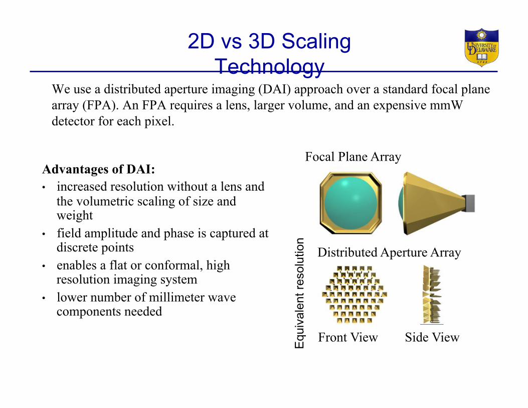
2D vs 3D Scaling Technology
We use a distributed aperture imaging (DAI) approach over a standard focal plane array (FPA). An FPA requires a lens, larger volume, and an expensive mmW detector for each pixel.
Advantages of DAI: • increased resolution without a lens and
the volumetric scaling of size and weight
• field amplitude and phase is captured at discrete points
• enables a flat or conformal, high resolution imaging system
• lower number of millimeter wave components needed E
quiv
alen
t res
olut
ion
Focal Plane Array
Distributed Aperture Array
Front View Side View
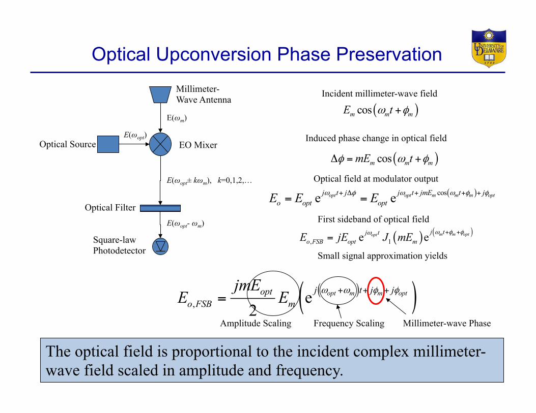
( )( ), e2
opt m m optj t j jopto FSB m
jmEE E ω ω φ φ+ + +
=
Optical Upconversion Phase Preservation
( )cosm m mmE tφ ω φΔ = +
( )cosm m mE tω φ+
( )cose eopt opt m m m optj t j j t jmE t jo opt optE E Eω φ ω ω φ φ+ Δ + + += =
( ) ( ), 1e e m m optopt j tj to FSB opt mE jE J mE ω φ φω + +
=
Incident millimeter-wave field
Induced phase change in optical field
Optical field at modulator output
First sideband of optical field
Small signal approximation yields
EO Mixer Optical Source
Optical Filter
Square-law Photodetector
Millimeter-Wave Antenna
E(ωopt)
E(ωm)
E(ωopt± kωm), k=0,1,2,…
E(ωopt- ωm)
Amplitude Scaling Frequency Scaling Millimeter-wave Phase
10 The optical field is proportional to the incident complex millimeter-wave field scaled in amplitude and frequency.
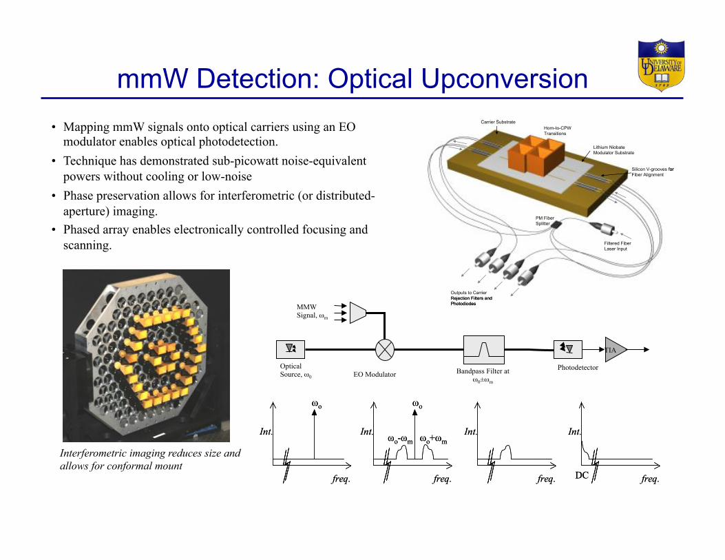
mmW Detection: Optical Upconversion
Filtered Fiber Laser Input
PM Fiber Splitter
Outputs to Carrier Rejection Filters and Photodiodes
Horn-to-CPW Transitions
Lithium NiobateModulator Substrate
Silicon V-grooves for Fiber Alignment
Carrier Substrate
Filtered Fiber Laser Input
PM Fiber Splitter
Outputs to Carrier Rejection Filters and Photodiodes
Horn-to-CPW Transitions
Lithium NiobateModulator Substrate
Silicon V-grooves for Fiber Alignment
Carrier Substrate
freq.
Int.
ωo
freq.
Int.
ωo
freq.
Int.
freq.
Int.
DC
ωo+ωmωo-ωm
A B C Dfreq.
Int.
ωo
freq.
Int.
ωo
freq.
Int.
freq.
Int.
DC
ωo+ωmωo-ωm
A B C D
TIA
Optical Source, ω0 EO Modulator Bandpass Filter at
ω0±ωm
Photodetector
MMW Signal, ωm
• Mapping mmW signals onto optical carriers using an EO modulator enables optical photodetection.
• Technique has demonstrated sub-picowatt noise-equivalent powers without cooling or low-noise
• Phase preservation allows for interferometric (or distributed-aperture) imaging.
• Phased array enables electronically controlled focusing and scanning.
Interferometric imaging reduces size and allows for conformal mount
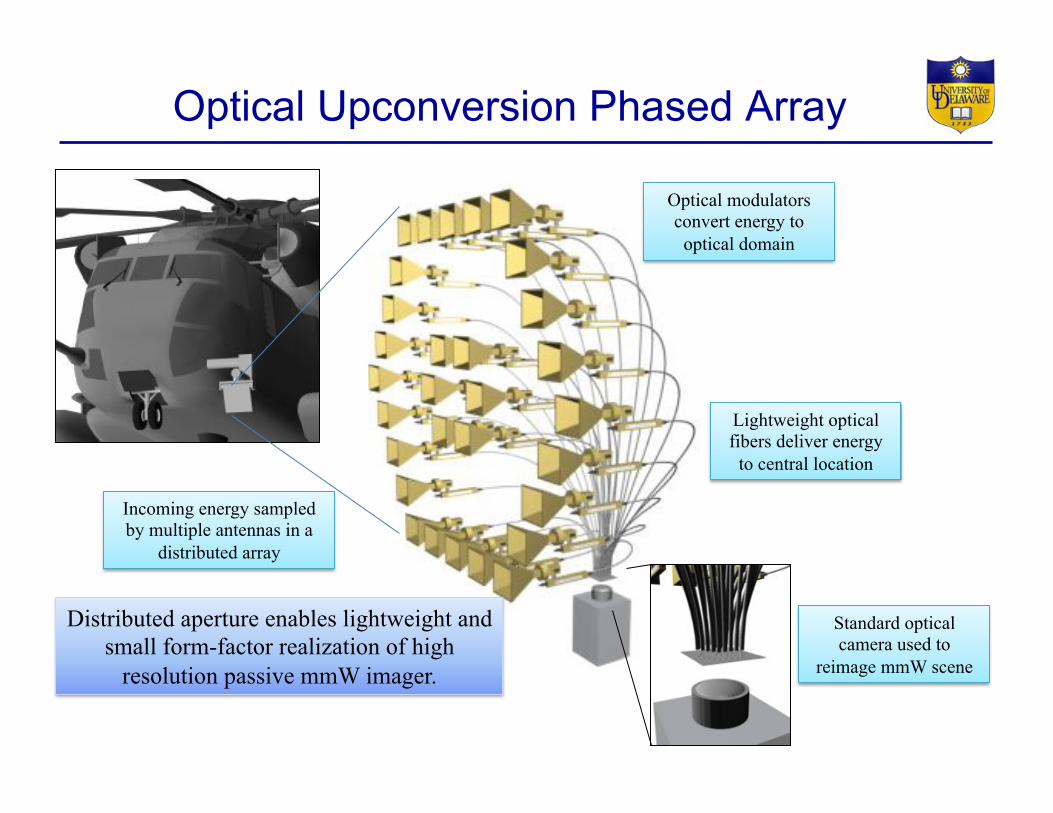
Optical Upconversion Phased Array
Incoming energy sampled by multiple antennas in a
distributed array
Optical modulators convert energy to
optical domain
Lightweight optical fibers deliver energy
to central location
Standard optical camera used to
reimage mmW scene
Distributed aperture enables lightweight and small form-factor realization of high
resolution passive mmW imager.
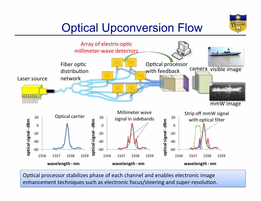
Laser&source&
Fiber&op.c&distribu.on&network&
Array&of&electro8op.c&millimeter8wave&detectors&
mmW&image&
visible&image&camera&Op.cal&processor&with&feedback&
Optical Upconversion Flow
!60
!40
!20
0
20
1556 1557 1558 1559optic
al(signal(,dB
m
wavelength(, nm
Optical2carrier
!60
!40
!20
0
20
1556 1557 1558 1559optic
al(signal(,d
Bm
wavelength(, nm
Millimeter2wave2signal2in2sidebands
!60
!40
!20
0
20
1556 1557 1558 1559optic
al(signal(,dB
mwavelength(, nm
Strip0off0mmW signalwith0optical0filter
Op.cal&processor&stabilizes&phase&of&each&channel&and&enables&electronic&image&enhancement&techniques&such&as&electronic&focus/steering&and&super8resolu.on.&
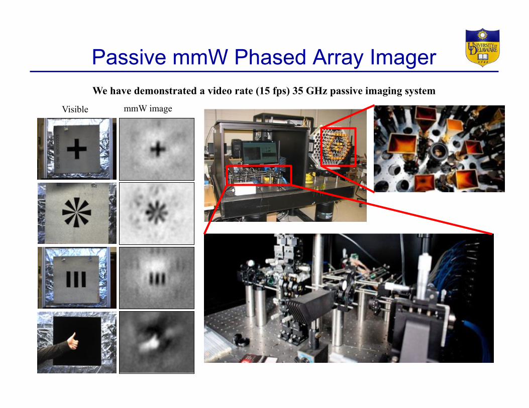
Passive mmW Phased Array Imager
Visible mmW image
We have demonstrated a video rate (15 fps) 35 GHz passive imaging system

Hand Passive Video
15
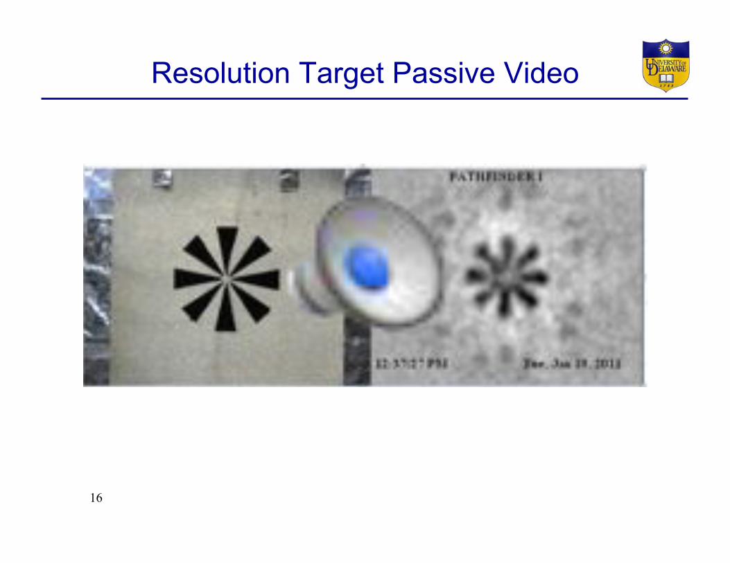
Resolution Target Passive Video
16
Passive W-Band Field Test Images
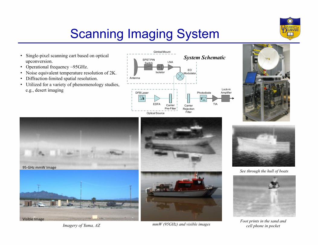
Scanning Imaging System
Imagery of Yuma, AZ
• Single-pixel scanning cart based on optical upconversion.
• Operational frequency ~95GHz. • Noise equivalent temperature resolution of 2K. • Diffraction-limited spatial resolution. • Utilized for a variety of phenomenology studies,
e.g., desert imaging
Antenna
SPST PIN Switch
Isolator
LNA
DFB Laser
EDFA Carrier Pre-Filter
Photodiode
TIA
Lock-in Amplifier
Carrier Rejection
Filter
Gimbal Mount
EO Modulator
Optical Source
System Schematic
Foot prints in the sand and cell phone in pocket mmW (95GHz) and visible images
958GHz&mmW&Image&
Visible&Image&&
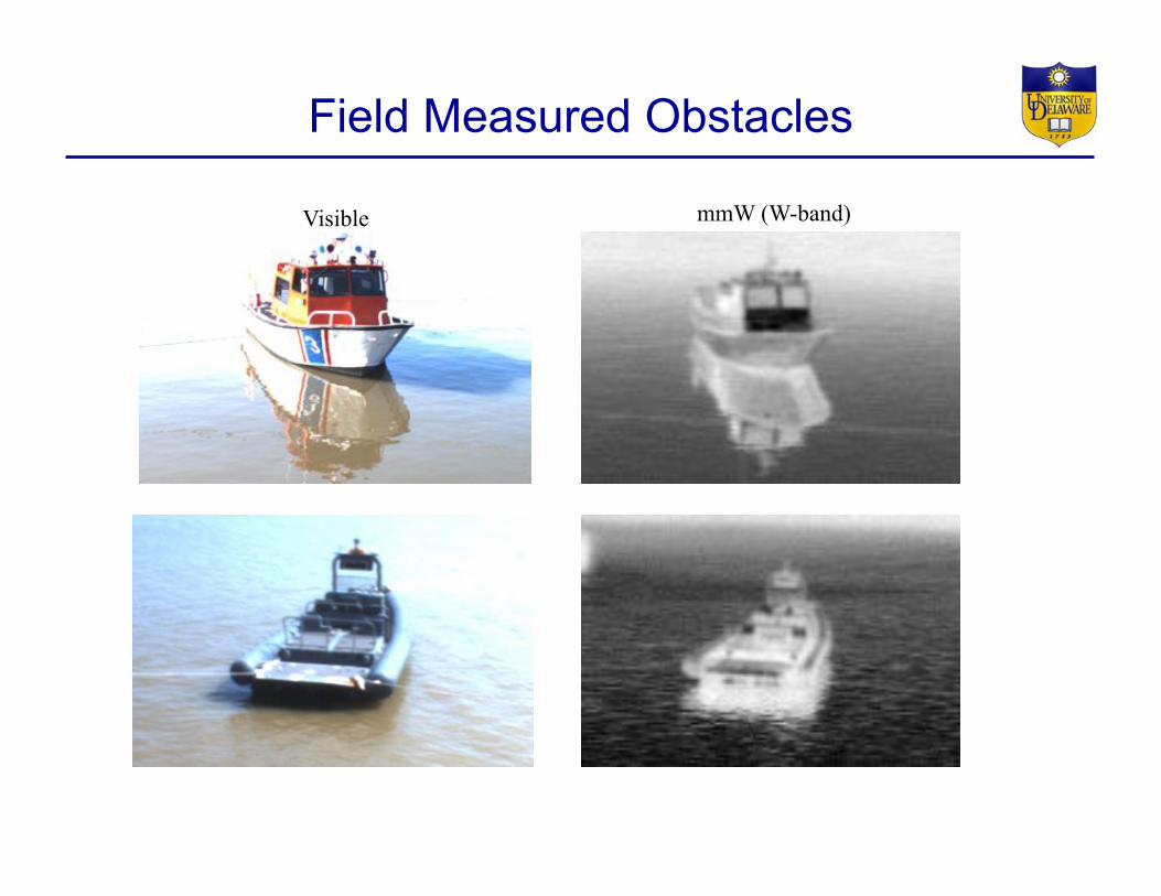
See through the hull of boats
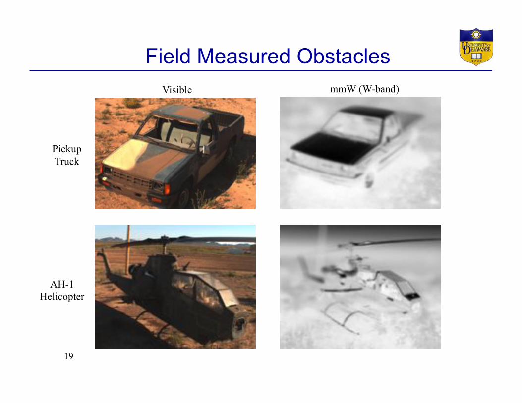
mmW (W-band) Visible
AH-1 Helicopter
Pickup Truck
Field Measured Obstacles
19
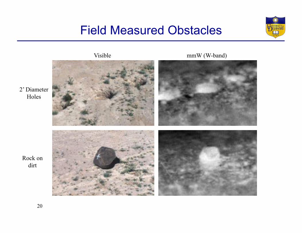
mmW (W-band) Visible
2’ Diameter Holes
Rock on dirt
Field Measured Obstacles
20
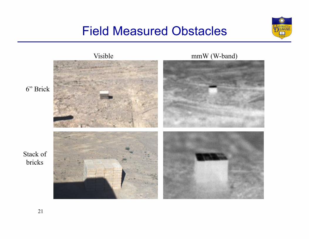
mmW (W-band) Visible
6” Brick
Stack of bricks
Field Measured Obstacles
21
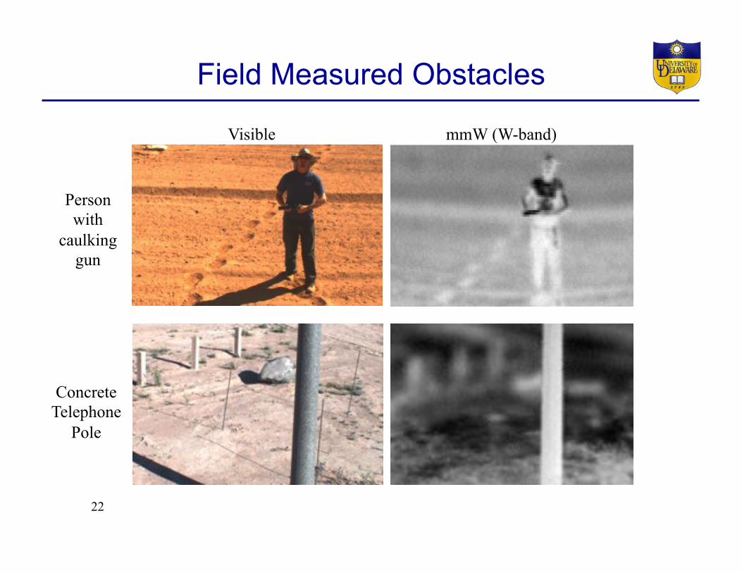
mmW (W-band) Visible
Person with
caulking gun
Concrete Telephone
Pole
Field Measured Obstacles
22
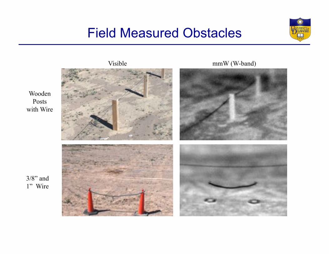
Field Measured Obstacles
Wooden Posts
with Wire
mmW (W-band) Visible
3/8” and 1” Wire

Field Measured Obstacles
Brick building
mmW (W-band) Visible
Adobe Hut
Field Measured Obstacles
mmW (W-band) Visible

Field Measured Obstacles
mmW (W-band) Visible

Field Measured Obstacles
mmW (W-band) Visible

Range of 100 feet at a declination angle of 27° Image of three targets on pavement: • Pair of bricks on end presenting ~7�x6� target (left) • 6� square aluminum plate (center) • Cinderblock (right)
Field Measured Obstacles

Can mmW’s Penetrate Brownout?

H-53 Helicopter at the Yuma Proving Grounds
Imaging Through Obscurants
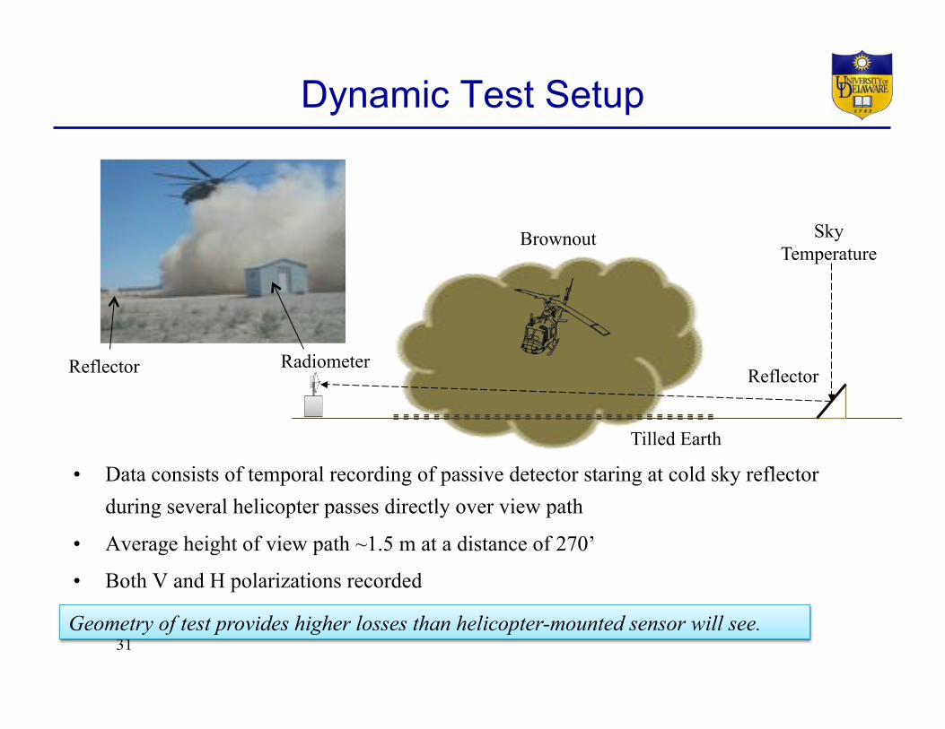
Dynamic Test Setup
• Data consists of temporal recording of passive detector staring at cold sky reflector during several helicopter passes directly over view path
• Average height of view path ~1.5 m at a distance of 270’
• Both V and H polarizations recorded
• Testing has been performed for UH-1, H-60, and H-53 generated dust
31
Radiometer
Tilled Earth
Brownout
Reflector
Sky Temperature
Reflector
Geometry of test provides higher losses than helicopter-mounted sensor will see.
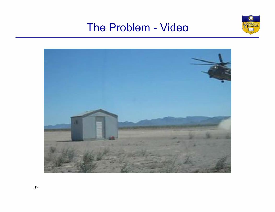
The Problem - Video
32
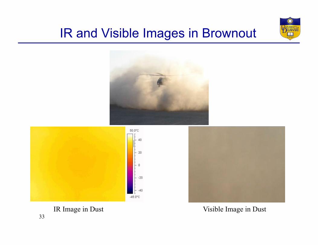
IR and Visible Images in Brownout
33 IR Image in Dust Visible Image in Dust

Brownout Field Testing Results
• Landing zone obstacles are clearly visible in mmW for all measured obstacles – Average contrast on the order of 15°C for H-polarization for ground targets tested
• mmW losses are low under all brownout conditions tested – Average maximum values of loss during all flyover tests: 1% for UH-1, 8% for H-60, 20% for H-53 over 150’ path
34
mmW and visible images of 2’ boulder, 2’ diameter holes, and person in Oasis LZ
Flyover testing demonstrates less than 20% contrast reduction for H-53 brownout at target operational range of 150’.
Radiometer
Tilled Earth
Brownout
Reflector
Sky Temperature
Passive mmW presents sufficient contrast in desert environments and impact of even worst case brownout attenuation is minimal.

How The Technology Works

mmW Detection: Optical Upconversion
Filtered Fiber Laser Input
PM Fiber Splitter
Outputs to Carrier Rejection Filters and Photodiodes
Horn-to-CPW Transitions
Lithium NiobateModulator Substrate
Silicon V-grooves for Fiber Alignment
Carrier Substrate
Filtered Fiber Laser Input
PM Fiber Splitter
Outputs to Carrier Rejection Filters and Photodiodes
Horn-to-CPW Transitions
Lithium NiobateModulator Substrate
Silicon V-grooves for Fiber Alignment
Carrier Substrate
freq.
Int.
ωo
freq.
Int.
ωo
freq.
Int.
freq.
Int.
DC
ωo+ωmωo-ωm
A B C Dfreq.
Int.
ωo
freq.
Int.
ωo
freq.
Int.
freq.
Int.
DC
ωo+ωmωo-ωm
A B C D
TIA
Optical Source, ω0 EO Modulator Bandpass Filter at
ω0±ωm
Photodetector
MMW Signal, ωm
• Mapping mmW signals onto optical carriers using an EO modulator enables optical photodetection.
• Technique has demonstrated sub-picowatt noise-equivalent powers without cooling or low-noise
• Phase preservation allows for interferometric (or distributed-aperture) imaging.
• Phased array enables electronically controlled focusing and scanning.
Interferometric imaging reduces size and allows for conformal mount
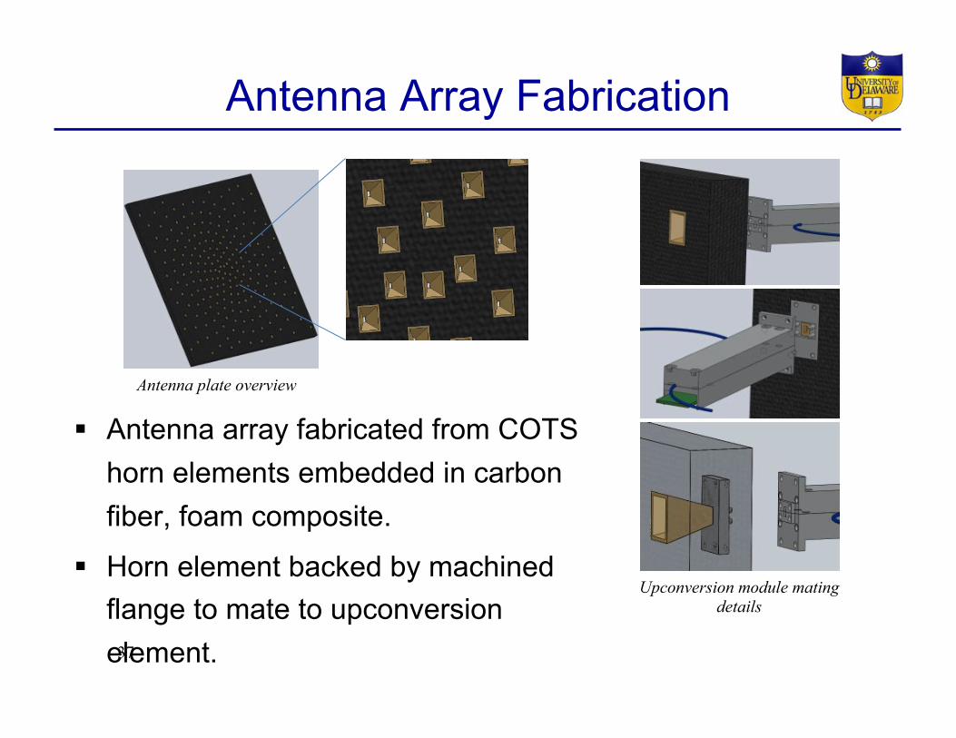
Antenna Array Fabrication
! Antenna array fabricated from COTS horn elements embedded in carbon fiber, foam composite.
! Horn element backed by machined flange to mate to upconversion element. 37
Antenna plate overview
Upconversion module mating details
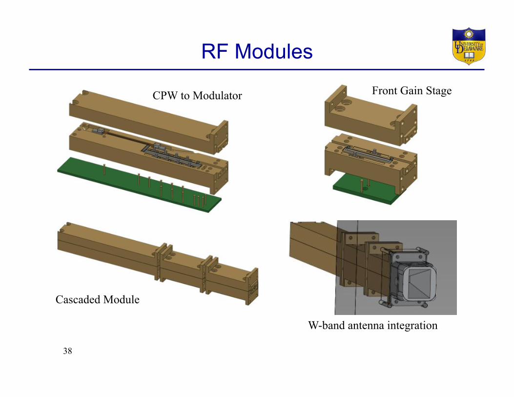
38
CPW to Modulator Front Gain Stage
Cascaded Module
W-band antenna integration
RF Modules

mmW Module Integration
EO Modulator
CPW with Amplifiers
Bottom Housing
PCB Control Board
RF In
Optical In
Detector module consists of metal housings, patterned alumina substrate, amplifiers, high speed EO modulator and PCB control board.
Fully integrated module with RF absorber filled top housing.
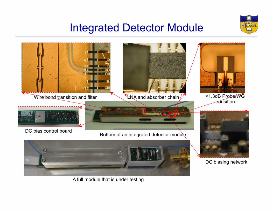
Integrated Detector Module
<1.3dB Probe/WG transition
LNA and absorber chain Wire bond transition and filter
DC bias control board Bottom of an integrated detector module
DC biasing network
A full module that is under testing

High Bandwidth Modulators
sw
Electrical Analysis
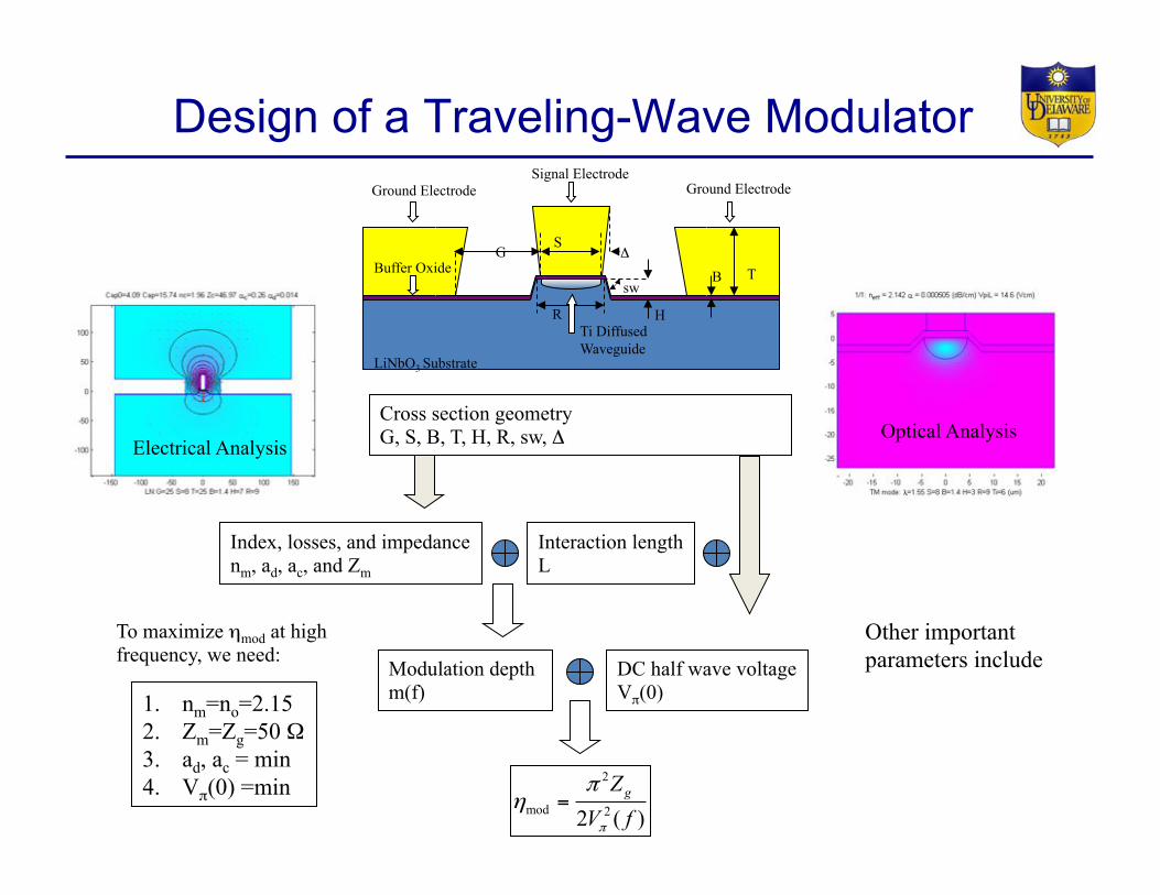
Design of a Traveling-Wave Modulator
Cross section geometry G, S, B, T, H, R, sw, Δ#
S Δ#
B
G T
H
Signal Electrode Ground Electrode Ground Electrode
Buffer Oxide
LiNbO3 Substrate
R Ti Diffused Waveguide
Index, losses, and impedance nm, ad, ac, and Zm
Interaction length L
DC half wave voltage Vπ(0)
Modulation depth m(f)
2
mod 22 ( )gZ
V fπ
πη =
Optical Analysis
1. nm=no=2.15 2. Zm=Zg=50 Ω 3. ad, ac = min 4. Vπ(0) =min
To maximize ηmod at high frequency, we need:
Other important parameters include

Modulation Efficiency Calculation
• Voltage on a traveling-wave modulator imposes phase change:
• Vπ(f) : voltage for
• Using transmission line theory:
CPW Electrodes, Impedance Zm, Effective Index nm
MMW Signal, Im Feed Impedance, Zg
Input optical power, Ii
Conduction Loss αc,Dielectric Loss,αd
MMW Termination Impedance, Zl
Optical Waveguide, Effective Index, no
Δφ =12"
#$%
&'n3rE 2πL
λ
"
#$
%
&'=
πn3rλ
"
#$
%
&'E x( )dx
0
L
∫ =πn3rλ
"
#$
%
&'V x( )ddx
0
L
∫
ηmod f( ) = π 2Zm2Vπ , f
2
!
"##
$
%&&=
π 2Zm2 Vπ ,DC ⋅m f( )( )
2
!
"
###
$
%
&&&
Dependends on Zm, |no- nm|, αc, and αd
= π
1Watts!
"#
$
%&
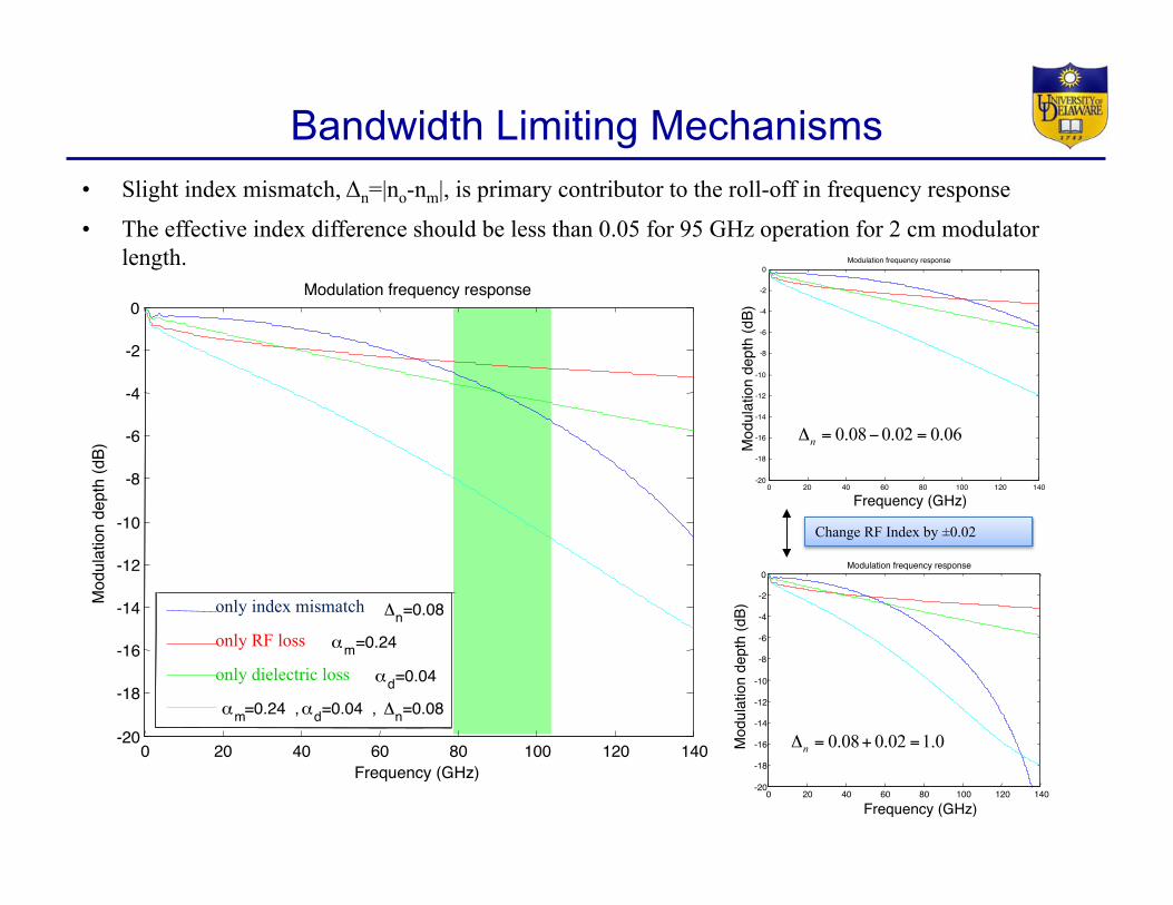
• Slight index mismatch, Δn=|no-nm|, is primary contributor to the roll-off in frequency response
• The effective index difference should be less than 0.05 for 95 GHz operation for 2 cm modulator length.
Change RF Index by ±0.02
0 20 40 60 80 100 120 140 -20
-18 -16 -14 -12 -10
-8 -6 -4 -2 0
Mod
ulat
ion
dept
h (d
B)
Frequency (GHz)
Modulation frequency response
only index mismatch only RF loss only dielectric loss
Δ n =0.08 α m =0.24
α d =0.04 α m =0.24 , α d =0.04 , Δ n =0.08
0 20 40 60 80 100 120 140 -20 -18 -16 -14 -12 -10
-8 -6 -4 -2 0
Mod
ulat
ion
dept
h (d
B)
Frequency (GHz)
Modulation frequency response
0.08 0.02 1.0nΔ = + =
0.08 0.02 0.06nΔ = − =
0 20 40 60 80 100 120 140 -20 -18 -16 -14 -12 -10 -8 -6 -4 -2 0
Mod
ulat
ion
dept
h (d
B)
Frequency (GHz)
Modulation frequency response
Bandwidth Limiting Mechanisms
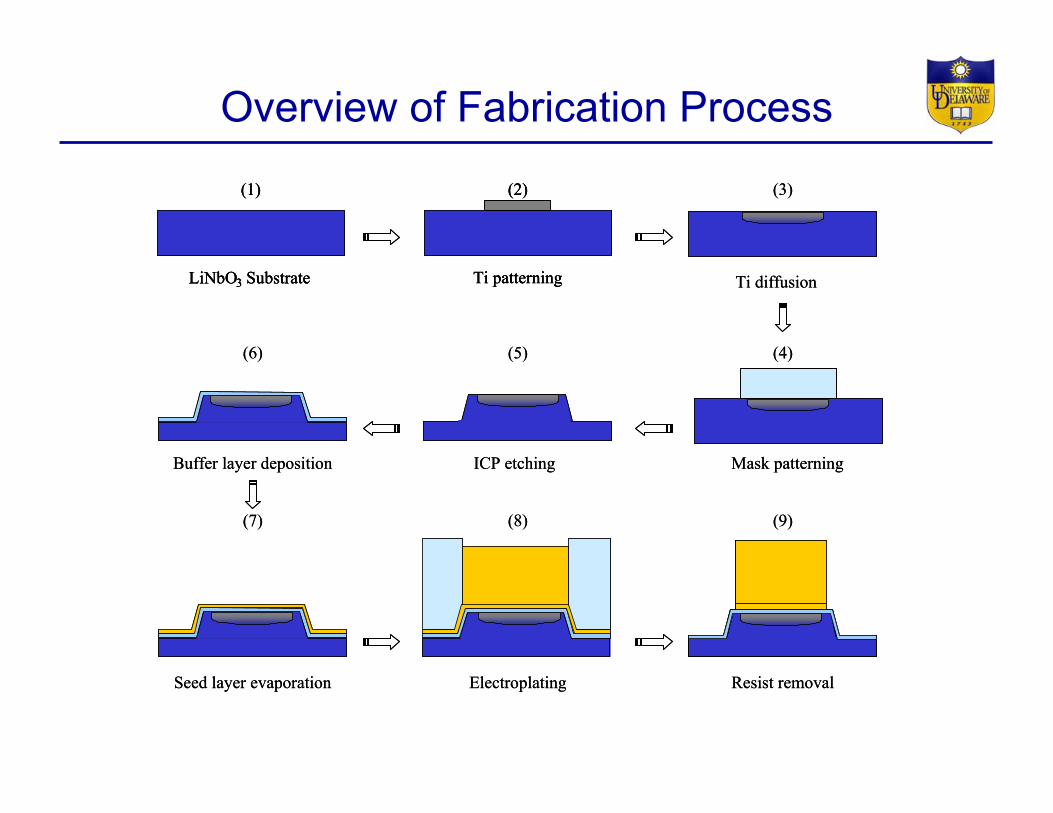
LiNbO3 Substrate
(1)
Ti diffusion
(3)
Seed layer evaporation
(7)
Resist removal
(9)
Electroplating
(8)
Ti patterning
(2)
Mask patterning
(4)
ICP etching
(5)(6)
Buffer layer deposition
LiNbO3 Substrate
(1)
LiNbO3 Substrate
(1)
Ti diffusion
(3)
Seed layer evaporation
(7)
Resist removal
(9)
Electroplating
(8)
Ti patterning
(2)
Ti patterning
(2)
Mask patterning
(4)
ICP etching
(5)(6)
Buffer layer deposition
Overview of Fabrication Process
Fabrication process
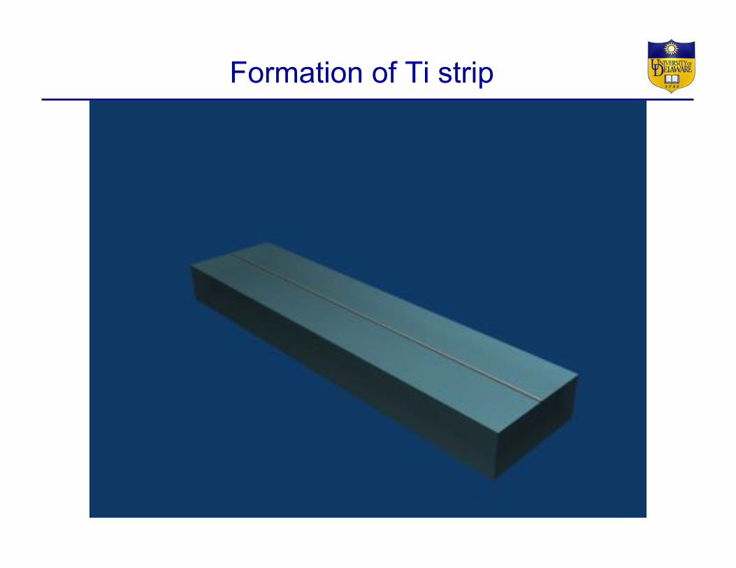
Formation of Ti strip
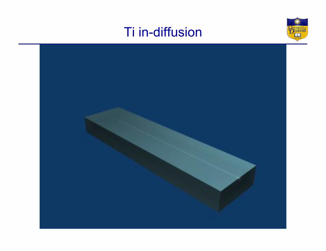
Ti in-diffusion
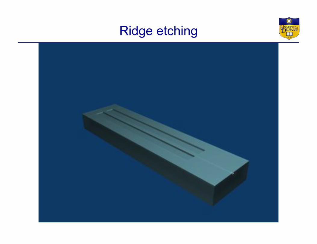
Ridge etching
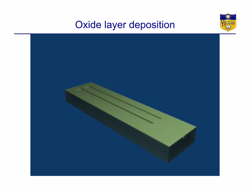
Oxide layer deposition
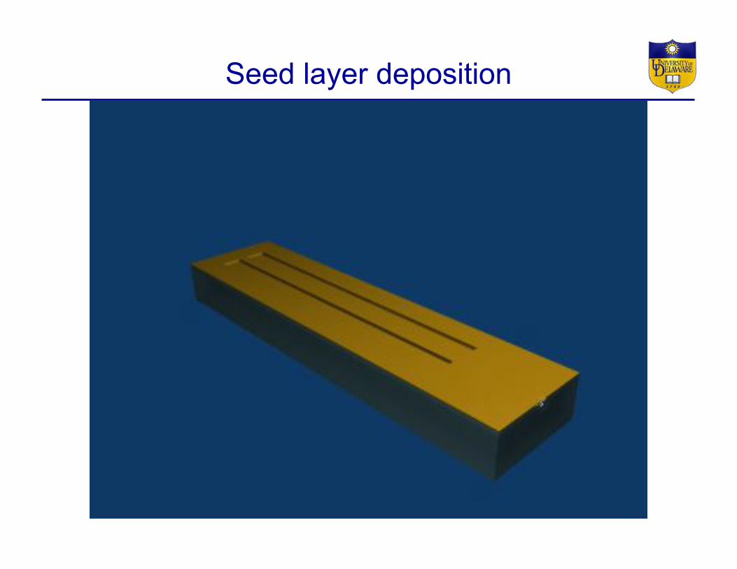
Seed layer deposition
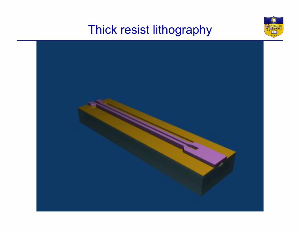
Thick resist lithography
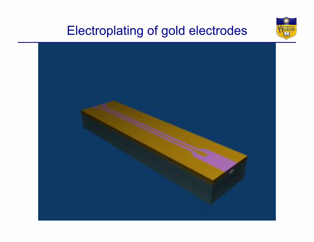
Electroplating of gold electrodes
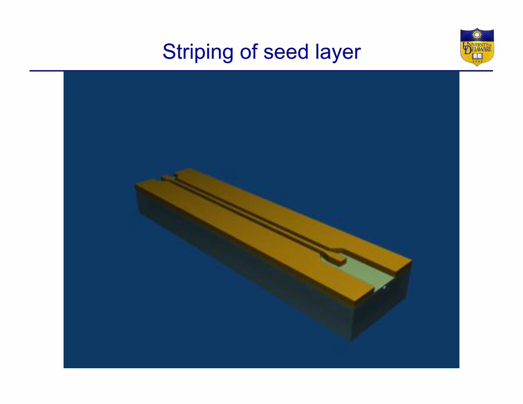
Striping of seed layer

Fabricated High Frequency Modulator
To mitigate the substrate mode, particularly at high frequencies (>50 GHz), the 500um thick LiNbO3 wafer was thinned on the backside of device. A trench with a width of 200um and depth of 450um is formed, thereby leaving a 50um thick device layer.
Modulator array Modulator feed Close view of modulator
Substrate thinning to eliminate substrate mode
Ti diffused optical waveguide 3.6 µm high ridge
24 µm thick electrodes
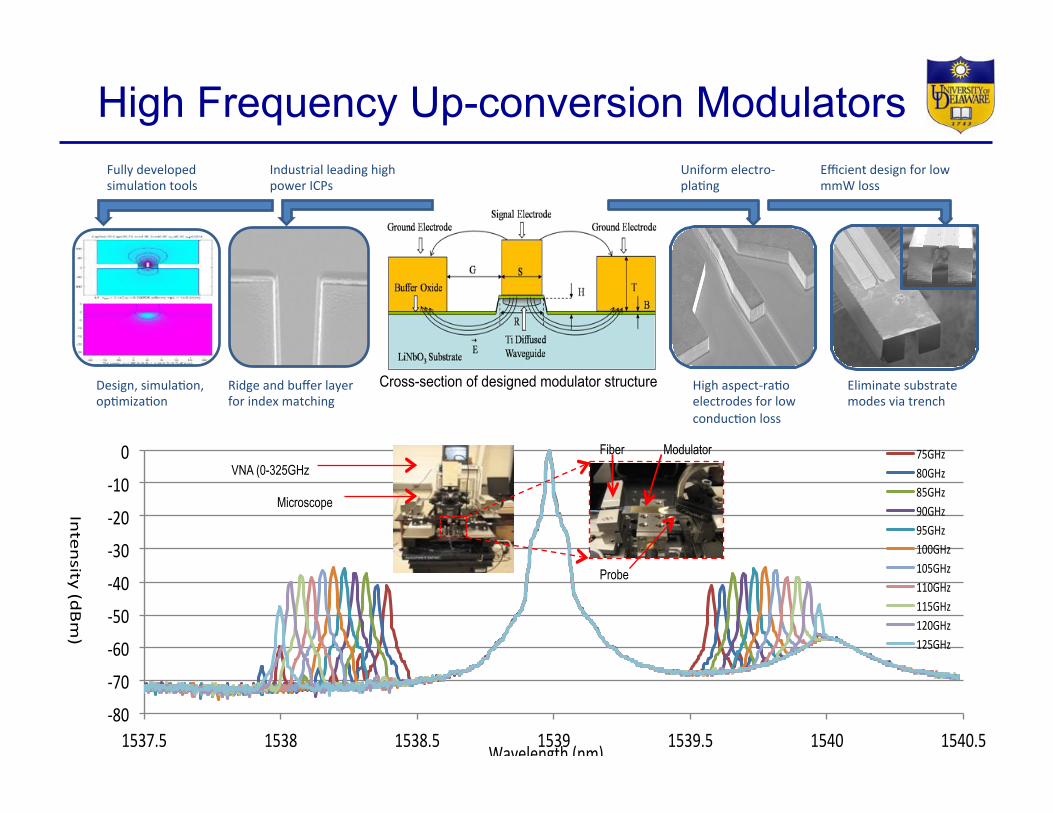
High Frequency Up-conversion Modulators
Design,&simula.on,&op.miza.on&&
Ridge&and&buffer&layer&&for&index&matching&
High&aspect8ra.o&electrodes&for&low&conduc.on&loss&
Eliminate&substrate&modes&via&trench&
Fully&developed&simula.on&tools&&
Industrial&leading&high&power&ICPs&
Uniform&electro8pla.ng&
Efficient&design&for&low&mmW&loss&
Cross-section of designed modulator structure
35GHz&modulator&
95GHz&modulator&
Design,(simula-on,(op-miza-on((
Ridge(and(buffer(layer(for(index(matching(
High(aspect=ra-o(electrodes(for(low(conduc-on(loss(
Low=loss(fin=coupled(transi-on(
Fully(developed(simula-on(tools((
Industrial(leading(high(power(ICPs(
Uniform(electro=pla-ng(
Efficient(design(for(mmW(coupling(
=80(
=70(
=60(
=50(
=40(
=30(
=20(
=10(
0(
1537.5( 1538( 1538.5( 1539( 1539.5( 1540( 1540.5(
75GHz(80GHz(85GHz(90GHz(95GHz(100GHz(105GHz(110GHz(115GHz(120GHz(125GHz(
Inten
sity((dBm)(
Wavelength((nm)(
VNA (0-325GHz
Microscope
Fiber Modulator
Probe
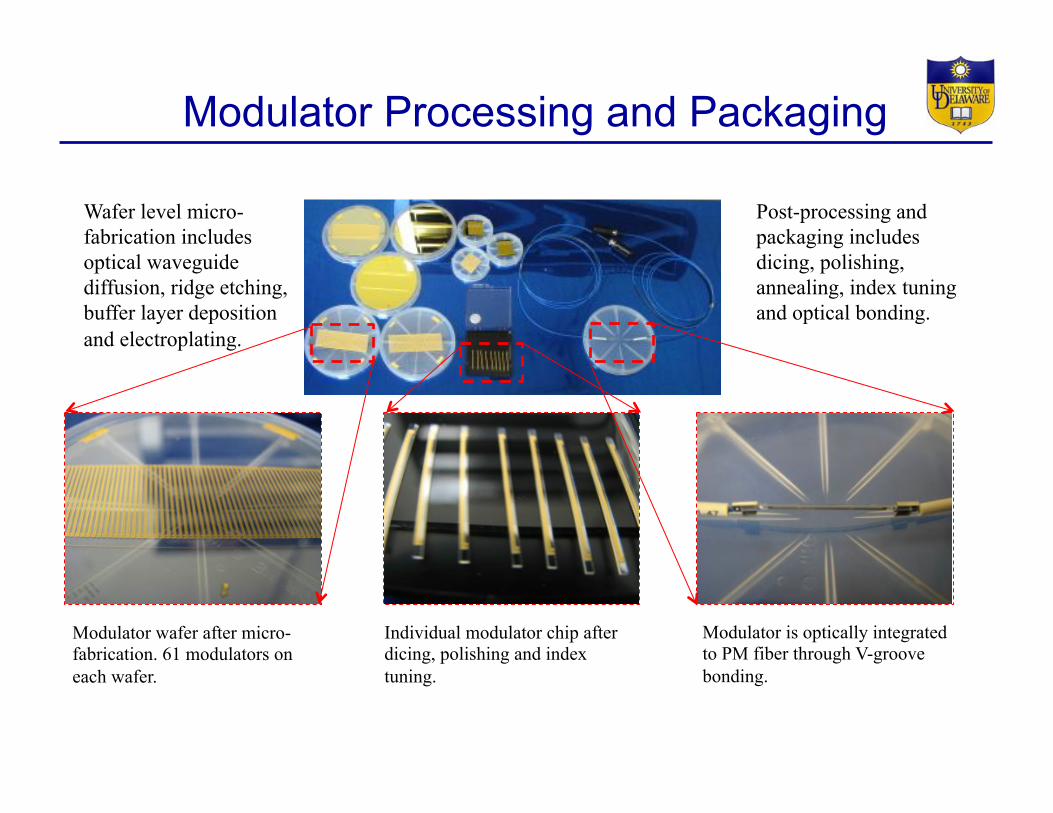
Modulator wafer after micro-fabrication. 61 modulators on each wafer.
Wafer level micro-fabrication includes optical waveguide diffusion, ridge etching, buffer layer deposition and electroplating.
Post-processing and packaging includes dicing, polishing, annealing, index tuning and optical bonding.
Individual modulator chip after dicing, polishing and index tuning.
Modulator is optically integrated to PM fiber through V-groove bonding.
Modulator Processing and Packaging
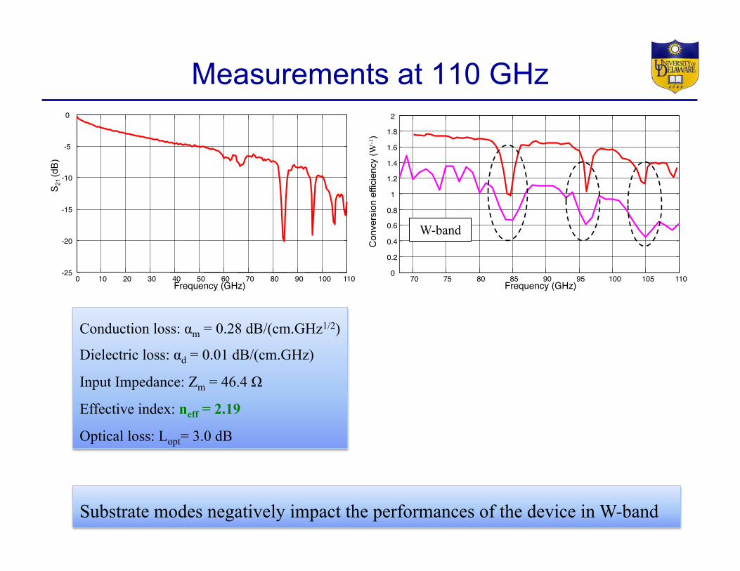
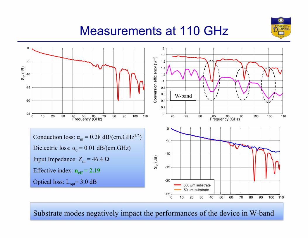
Measurements at 110 GHz
0 10 20 30 40 50 60 70 80 90 100 110 -25
-20
-15
-10
-5
0
70 75 80 85 90 95 100 105 110 0 0.2 0.4 0.6 0.8 1
1.2 1.4 1.6 1.8 2
Frequency (GHz) Frequency (GHz)
Substrate modes negatively impact the performances of the device in W-band
Con
vers
ion
effic
ienc
y (W
-1)
S21
(dB
)
Conduction loss: αm = 0.28 dB/(cm.GHz1/2)
Dielectric loss: αd = 0.01 dB/(cm.GHz)
Input Impedance: Zm = 46.4 Ω
Effective index: neff = 2.19
Optical loss: Lopt= 3.0 dB
W-band
0 10 20 30 40 50 60 70 80 90 100 110 -25
-20
-15
-10
-5 0
500 µm substrate 50 µm substrate
S21
(dB
)
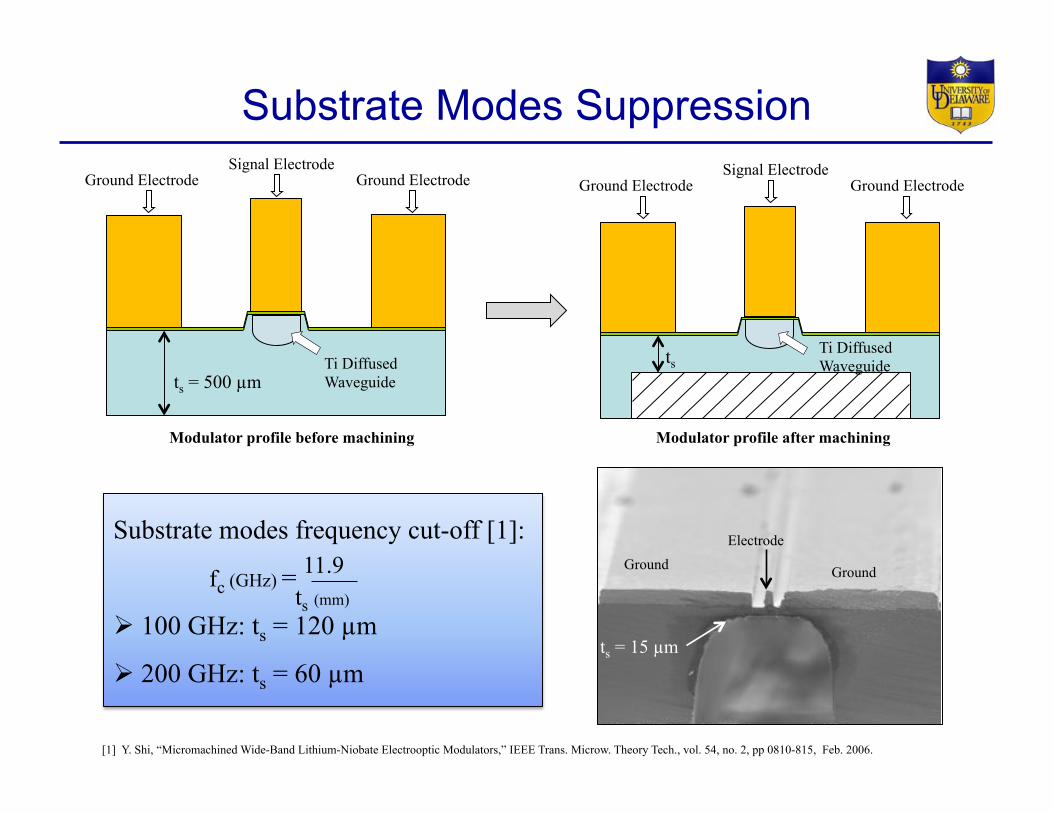
Substrate Modes Suppression
Modulator profile before machining
Modulator profile after machining
ts = 500 µm E
ts
Substrate modes frequency cut-off [1]:
fc (GHz) =
" 100 GHz: ts = 120 µm
" 200 GHz: ts = 60 µm
Ti Diffused Waveguide
Signal Electrode Ground Electrode Ground Electrode
Ti Diffused Waveguide
Signal Electrode Ground Electrode Ground Electrode
ts = 15 µm
Electrode
Ground Ground
ts (mm)
11.9
[1] Y. Shi, “Micromachined Wide-Band Lithium-Niobate Electrooptic Modulators,” IEEE Trans. Microw. Theory Tech., vol. 54, no. 2, pp 0810-815, Feb. 2006.

High Bandwidth Operation
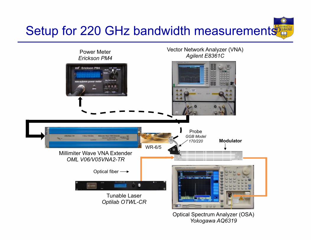
Setup for 220 GHz bandwidth measurements Vector Network Analyzer (VNA)
Agilent E8361C
Optical Spectrum Analyzer (OSA) Yokogawa AQ6319
Millimiter Wave VNA Extender OML V06/V05VNA2-TR
WR-6/5 Modulator
Tunable Laser Optilab OTWL-CR
Probe GGB Model
170/220
Power Meter Erickson PM4
Optical fiber
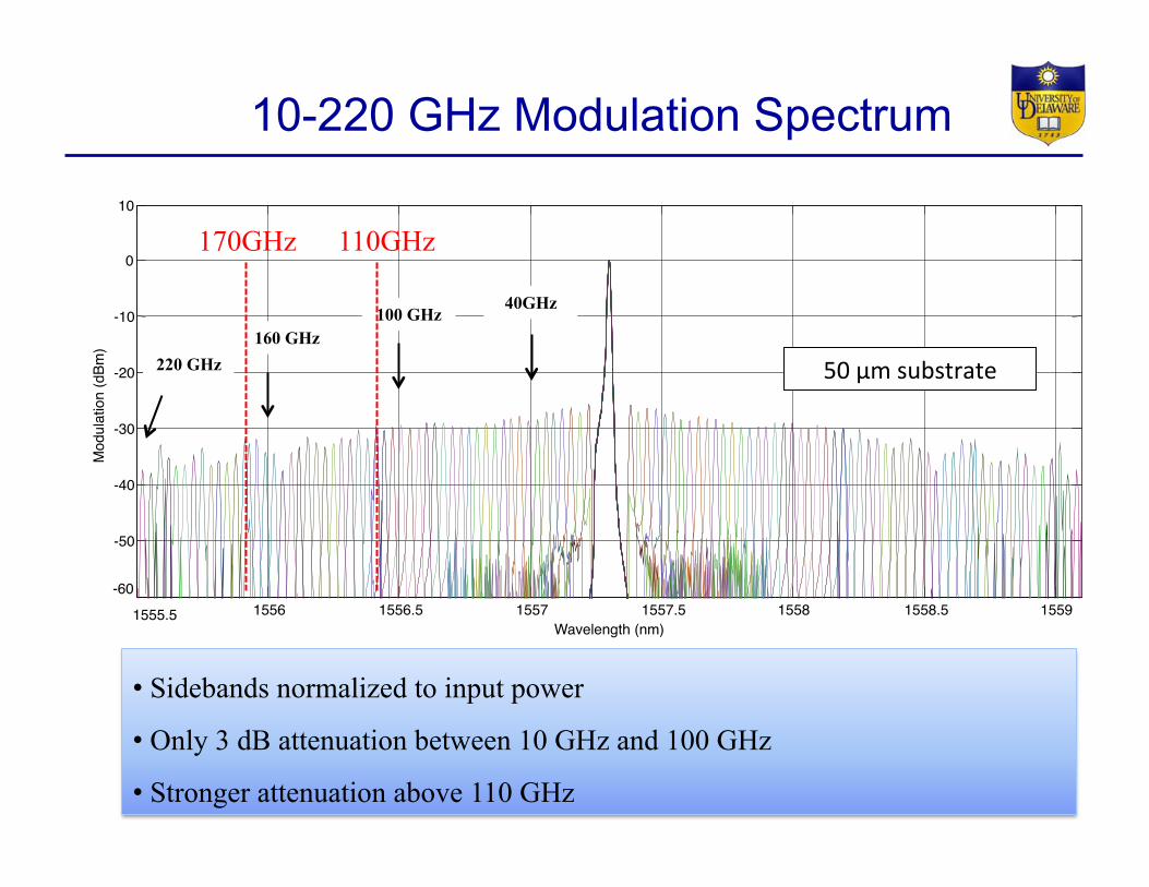
1555.5 1556 1556.5 1557 1557.5 1558 1558.5 1559 -60
-50
-40
-30
-20
-10
0
10
Wavelength (nm)
Mod
ulat
ion
(dBm
)
40GHz
160 GHz 220 GHz
100 GHz
10-220 GHz Modulation Spectrum
50&µm&substrate&
• Sidebands normalized to input power
• Only 3 dB attenuation between 10 GHz and 100 GHz
• Stronger attenuation above 110 GHz
170GHz 110GHz
Ultra-Wideband Frequency Synthesis
Why Optical Generation of RF Sources?
• Ultra-wide tuning range – Small tuning range in optical domain
= huge tuning range in RF (200 GHz = 1.6 nm)
• RF distribution for remote LO sources, phased arrays – RF over fiber = transmit over km’s with negligible loss/
dispersion
• Phase steering in optical domain, UWB – Phase is preserved in optical-to-RF conversion = fast, low-
power, wide-BW, low-dispersion phase steering in optical domain
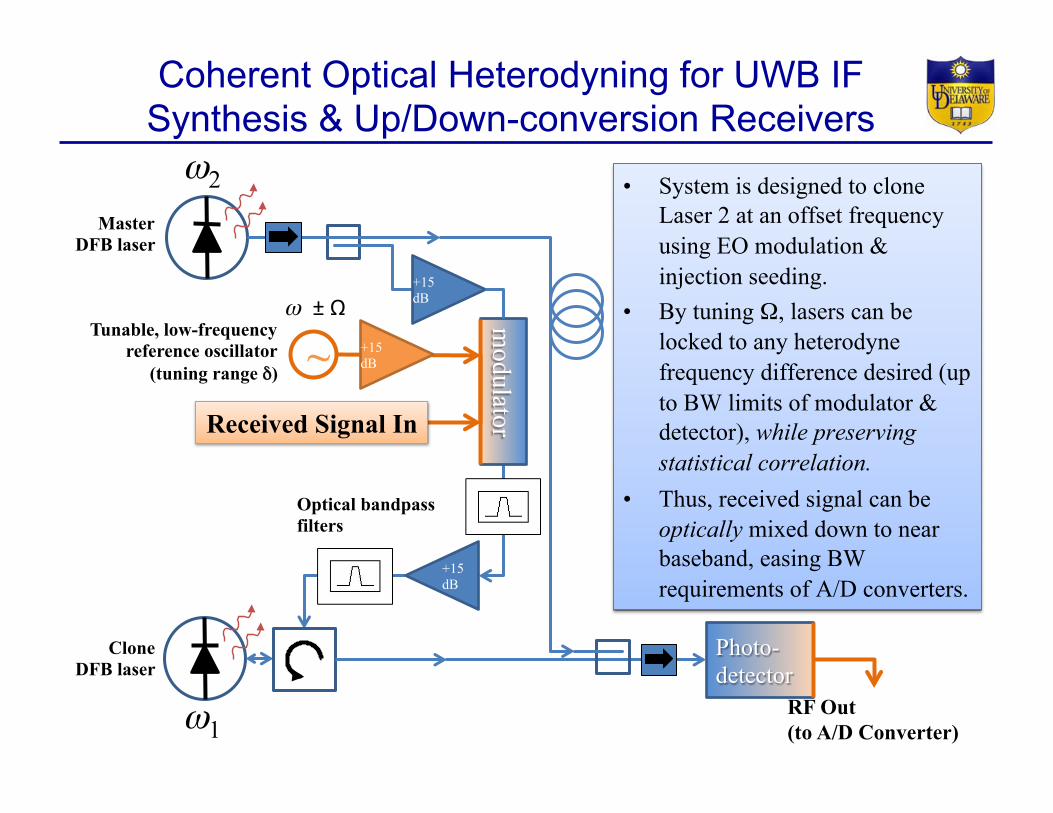
Coherent Optical Heterodyning for UWB IF Synthesis & Up/Down-conversion Receivers
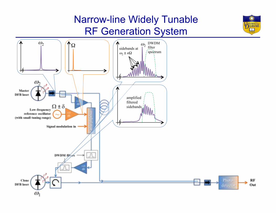
• System is designed to clone Laser 2 at an offset frequency using EO modulation & injection seeding.
• By tuning Ω, lasers can be locked to any heterodyne frequency difference desired (up to BW limits of modulator & detector), while preserving statistical correlation.
• Thus, received signal can be optically mixed down to near baseband, easing BW requirements of A/D converters.
Photo-detector
ω1
ω2
RF Out (to A/D Converter)
+15 dB
+15 dB
Received Signal In
~Tunable, low-frequency
reference oscillator (tuning range δ)
modulator
+15 dB
Master DFB laser
Clone DFB laser
ω ±&Ω
Optical bandpass filters
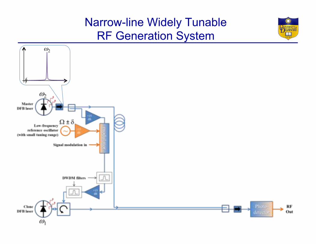
Narrow-line Widely Tunable RF Generation System
ω2
Narrow-line Widely Tunable RF Generation System
ω2 Ω
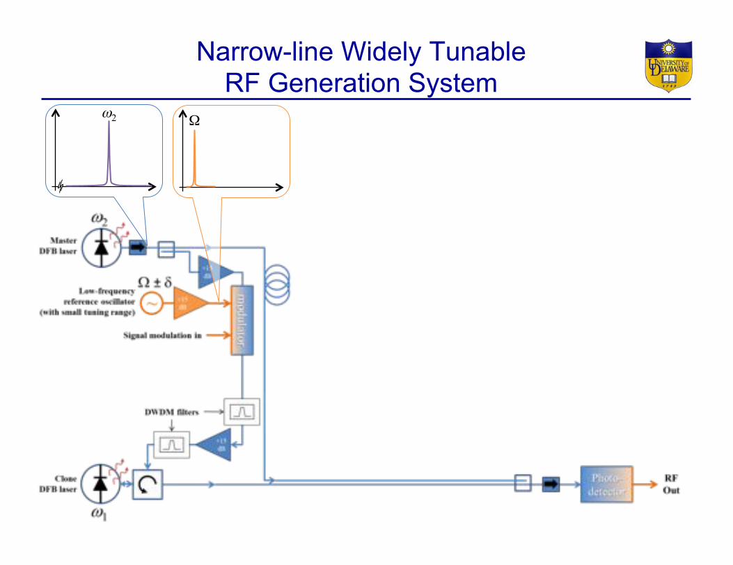
Narrow-line Widely Tunable RF Generation System
ω2 Ω ω2 sidebands at ω2 ± nΩ#
DWDM filter spectrum
Narrow-line Widely Tunable RF Generation System
ω2 Ω ω2 sidebands at ω2 ± nΩ#
DWDM filter spectrum
amplified filtered sidebands
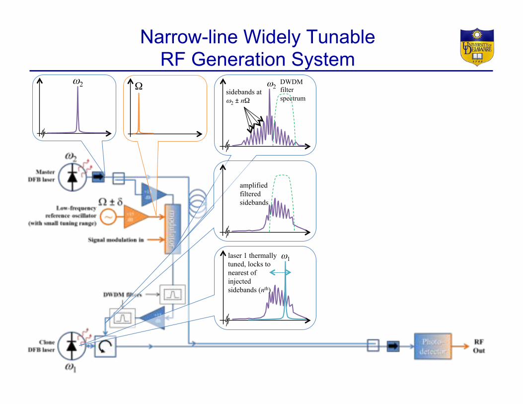
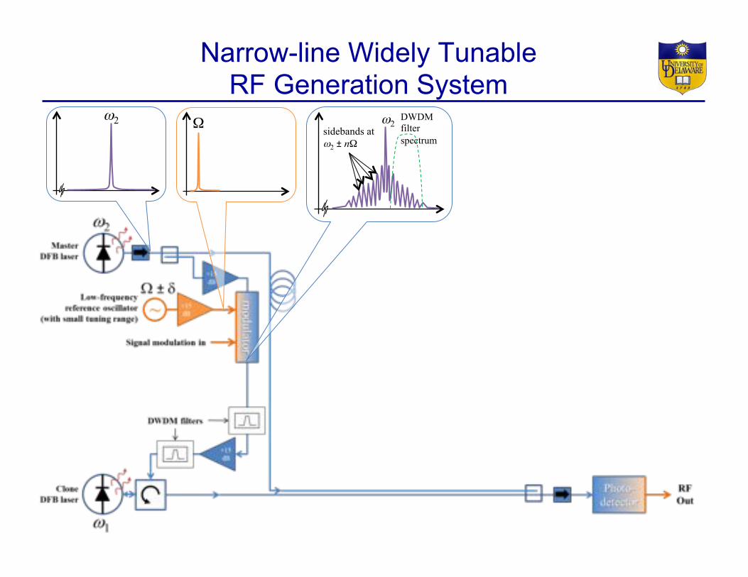
Narrow-line Widely Tunable RF Generation System
ω2 Ω ω2 sidebands at ω2 ± nΩ#
DWDM filter spectrum
amplified filtered sidebands
ω1 laser 1 thermally tuned, locks to nearest of injected sidebands (nth)
Narrow-line Widely Tunable RF Generation System
ω2 Ω ω2 sidebands at ω2 ± nΩ#
DWDM filter spectrum
amplified filtered sidebands
ω1 laser 1 thermally tuned, locks to nearest of injected sidebands (nth)
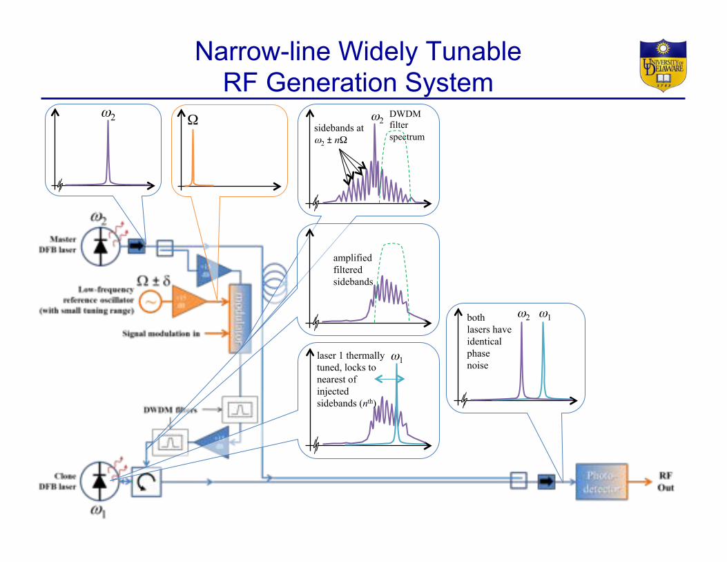
ω1 ω2 both lasers have identical phase noise

Narrow-line Widely Tunable RF Generation System
ω2 Ω ω2 sidebands at ω2 ± nΩ#
DWDM filter spectrum
amplified filtered sidebands
ω1 laser 1 thermally tuned, locks to nearest of injected sidebands (nth)
ω1 ω2 both lasers have identical phase noise
fine tuning range = nδ#
Ω nΩ
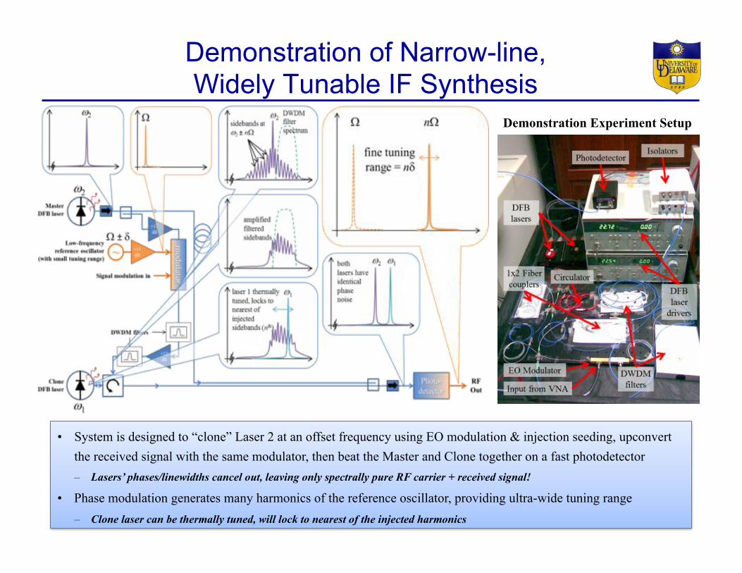
Demonstration of Narrow-line, Widely Tunable IF Synthesis
• System is designed to “clone” Laser 2 at an offset frequency using EO modulation & injection seeding, upconvert the received signal with the same modulator, then beat the Master and Clone together on a fast photodetector – Lasers’ phases/linewidths cancel out, leaving only spectrally pure RF carrier + received signal!
• Phase modulation generates many harmonics of the reference oscillator, providing ultra-wide tuning range – Clone laser can be thermally tuned, will lock to nearest of the injected harmonics
Demonstration Experiment Setup

Coherent Optical Heterodyne Receivers: Summary of Accomplishments
• Linewidth of 1-2 Hz has been demonstrated over a range from 0.6-49 GHz (upper limit is photodetector bandwidth)
• Thermally tuned DFB grating in clone laser provides built-in filtering which allows locking to single sideband when injecting of a comb of harmonics derived from a common reference
• Lasers can be locked to harmonics of the reference-oscillator frequency—locking has been demonstrated with 2nd through 10th harmonics, demonstrating wide tunability of RF from a single, low-frequency reference, while preserving the optical phase-noise cancellation from injection locking
Phase noise of RF signal from locked lasers at several carrier frequencies.
Measured RF Spectra from Locked Lasers
Zoom to 100-Hz span
RF spectra when modulating a 12-GHz carrier with various 2-MHz waveforms
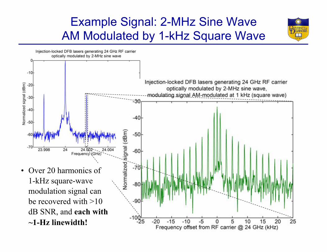
Example Signal: 2-MHz Sine Wave AM Modulated by 1-kHz Square Wave
• Over 20 harmonics of 1-kHz square-wave modulation signal can be recovered with >10 dB SNR, and each with ~1-Hz linewidth!
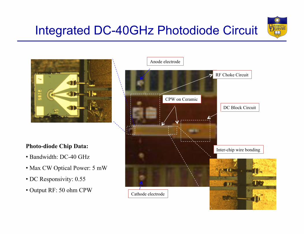
Integrated DC-40GHz Photodiode Circuit
Inter-chip wire bonding
Anode electrode
Cathode electrode
RF Choke Circuit
DC Block Circuit
Photo-diode Chip Data:
• Bandwidth: DC-40 GHz
• Max CW Optical Power: 5 mW
• DC Responsivity: 0.55
• Output RF: 50 ohm CPW
CPW on Ceramic

Ultra-wideband Integrated Power Amplifier Characterization setup
Ceramic CPW chip
0! 5! 10! 15! 20! 25! 30! 35! 40! 45! 50!-70!
-60!
-50!
-40!
-30!
-20!
-10!
0!
10!
20!
Frequency (GHz)!
S-pa
ram
eter
s (dB
)!
!
!
S11!S21!S12!S22!
0 5 10 15 20 25 30 35 40 45 50 -200 -150 -100 -50 0
50 100 150 200
Frequency (GHz)
S21
(deg
)
~15 dB Gain
Measured Phase
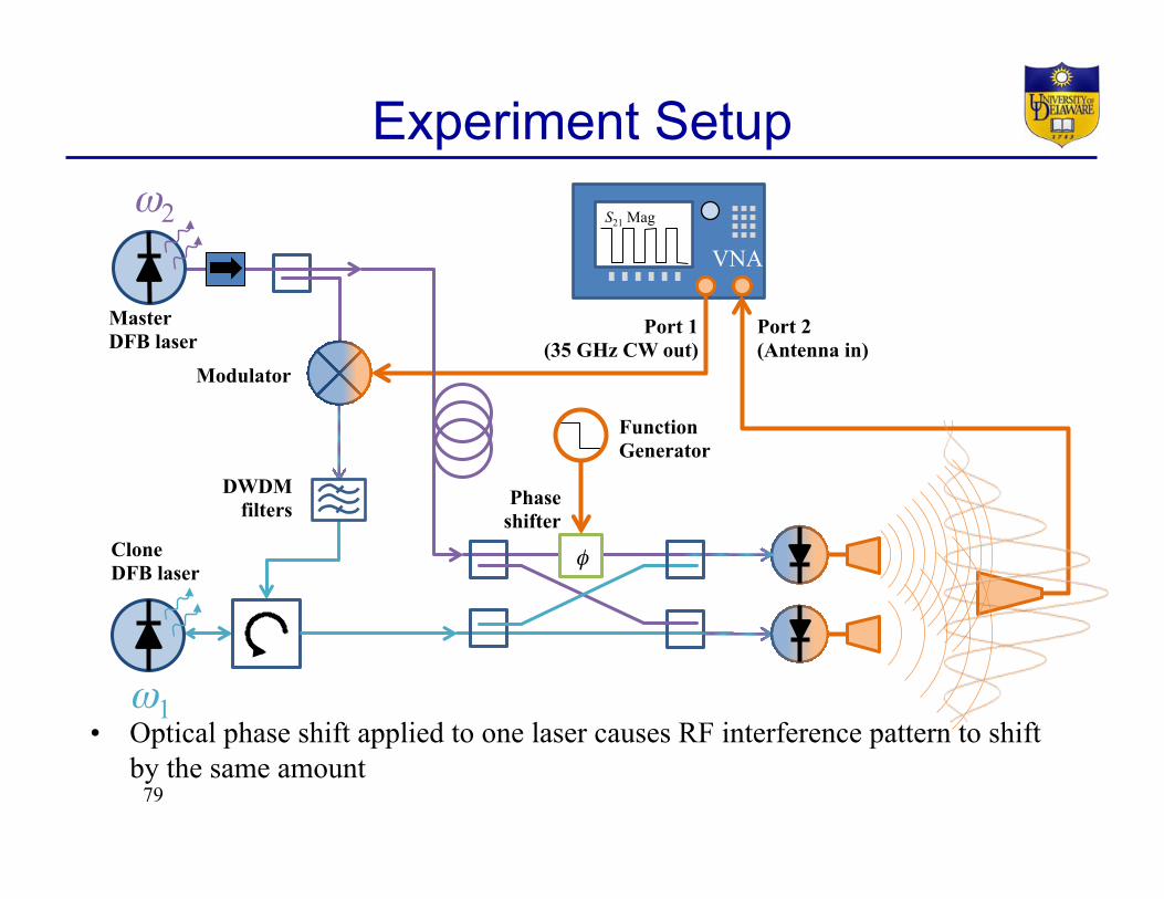
Experiment Setup
• Optical phase shift applied to one laser causes RF interference pattern to shift by the same amount
VNA
Port 1 (35 GHz CW out)
Master DFB laser
Clone DFB laser
DWDM filters
ω1
ω2
φ$
Function Generator
Modulator
Phase shifter
Port 2 (Antenna in)
S21 Mag
79

Optically-fed Phased Array Demonstration
Top
view
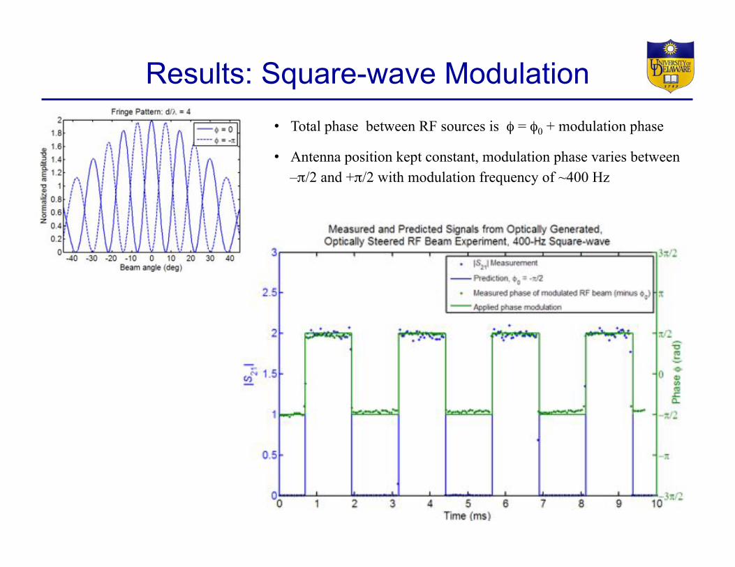
Results: Square-wave Modulation • Total phase between RF sources is φ = φ0 + modulation phase
• Antenna position kept constant, modulation phase varies between –π/2 and +π/2 with modulation frequency of ~400 Hz

Integrated Silicon RF Photonics
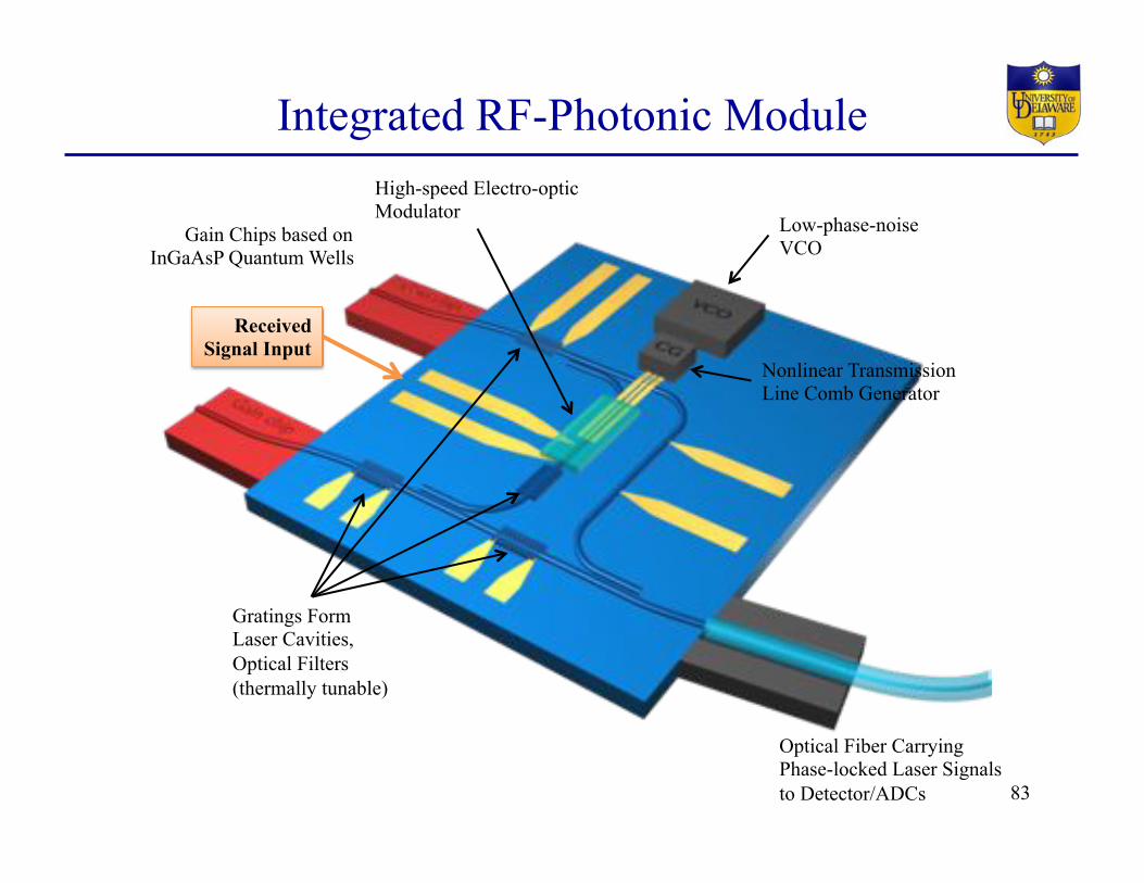
Integrated RF-Photonic Module
Low-phase-noise VCO
Nonlinear Transmission Line Comb Generator
Optical Fiber Carrying Phase-locked Laser Signals to Detector/ADCs
Gain Chips based on InGaAsP Quantum Wells
Gratings Form Laser Cavities, Optical Filters (thermally tunable)
High-speed Electro-optic Modulator
Received Signal Input
83
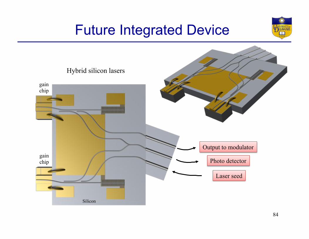
Future Integrated Device
Output to modulator
Photo detector
Laser seed
Hybrid silicon lasers
Silicon
gain chip
gain chip
84
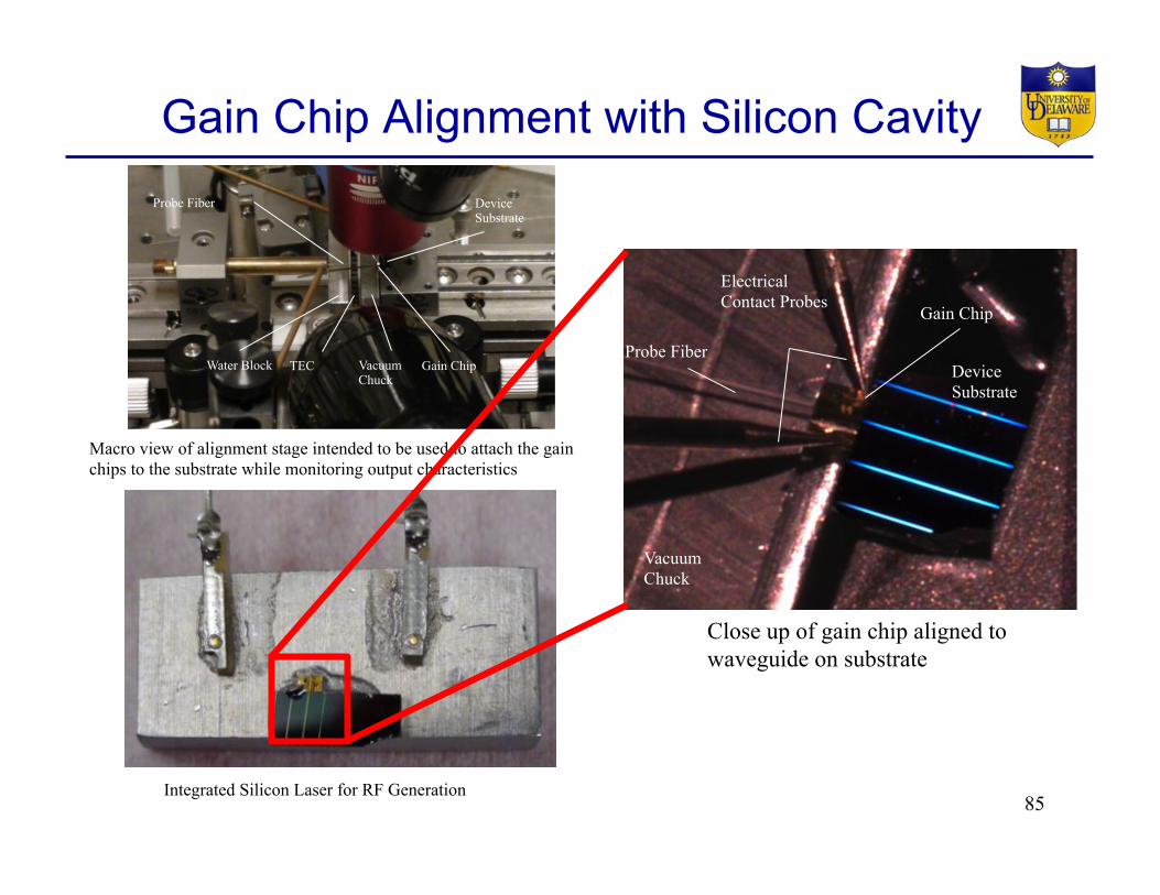
Gain Chip Alignment with Silicon Cavity
Macro view of alignment stage intended to be used to attach the gain chips to the substrate while monitoring output characteristics
Probe Fiber
Vacuum Chuck
Gain Chip Device Substrate
Probe Fiber
Vacuum Chuck
Gain Chip
Device Substrate
Water Block TEC Probe Fiber
Vacuum Chuck
Gain Chip
Device Substrate
Electrical Contact Probes
Close up of gain chip aligned to waveguide on substrate
Integrated Silicon Laser for RF Generation 85
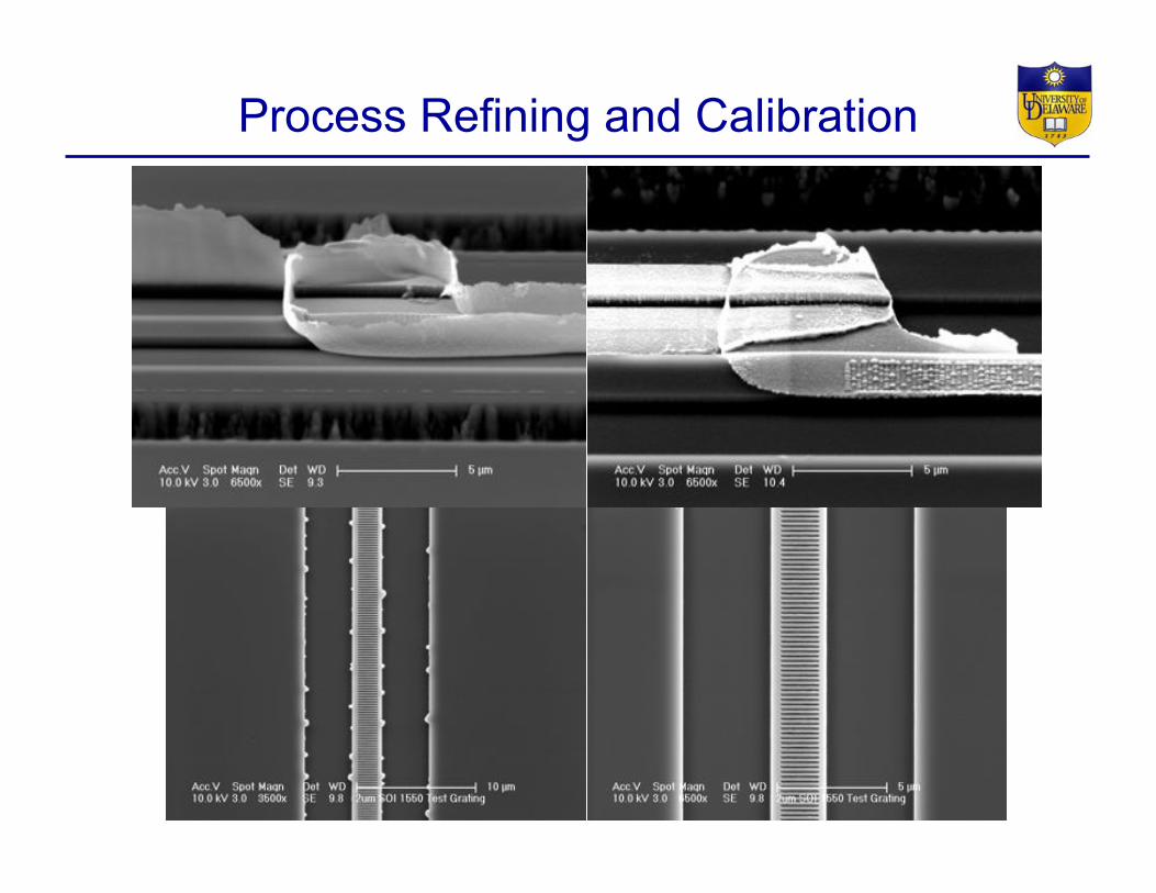
Process Refining and Calibration

Testing Setup

Tuning Distributed Bragg reflector (DBR)
• Tunes at approximately 0.09 nm/ºC
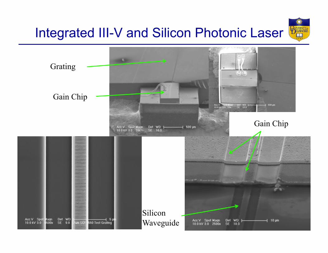
Integrated III-V and Silicon Photonic Laser
Gain Chip
Grating
Gain Chip
Waveguide
Silicon Waveguide
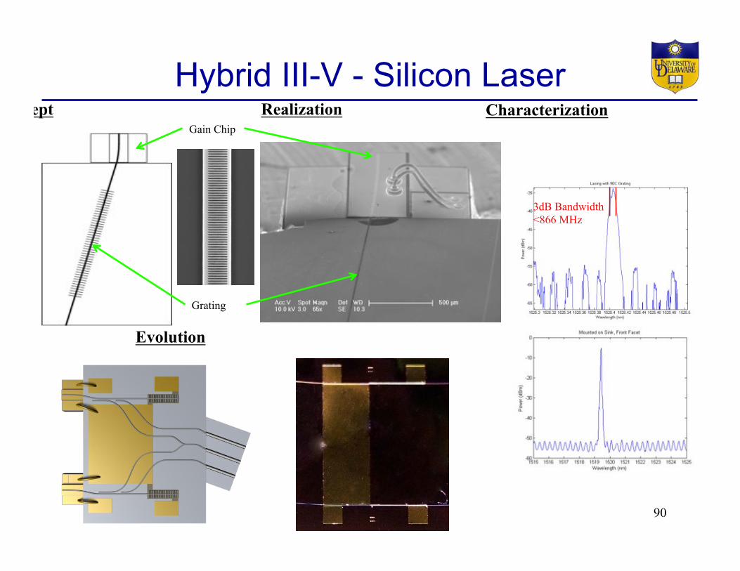
Hybrid III-V - Silicon Laser Gain Chip
Realization Concept Characterization
Grating
3dB Bandwidth <866 MHz
Evolution
90
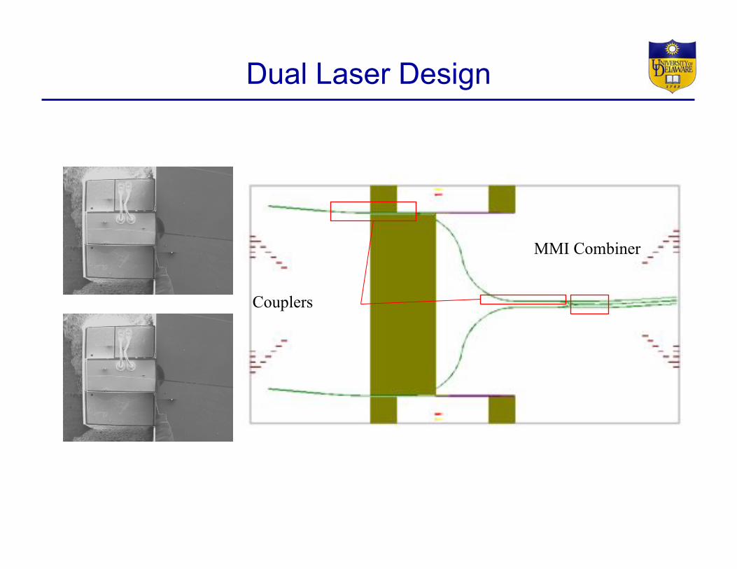
Dual Laser Design
Couplers
MMI Combiner
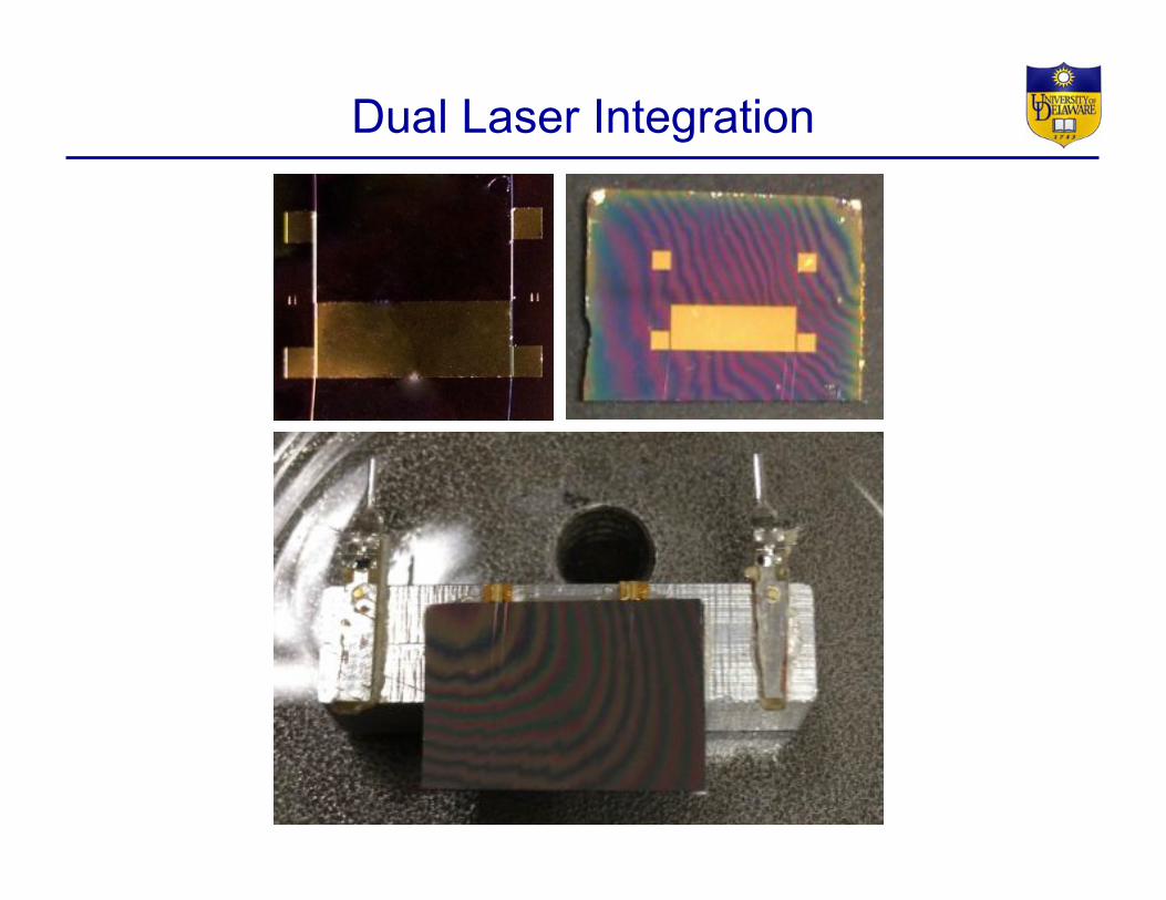
Dual Laser Integration
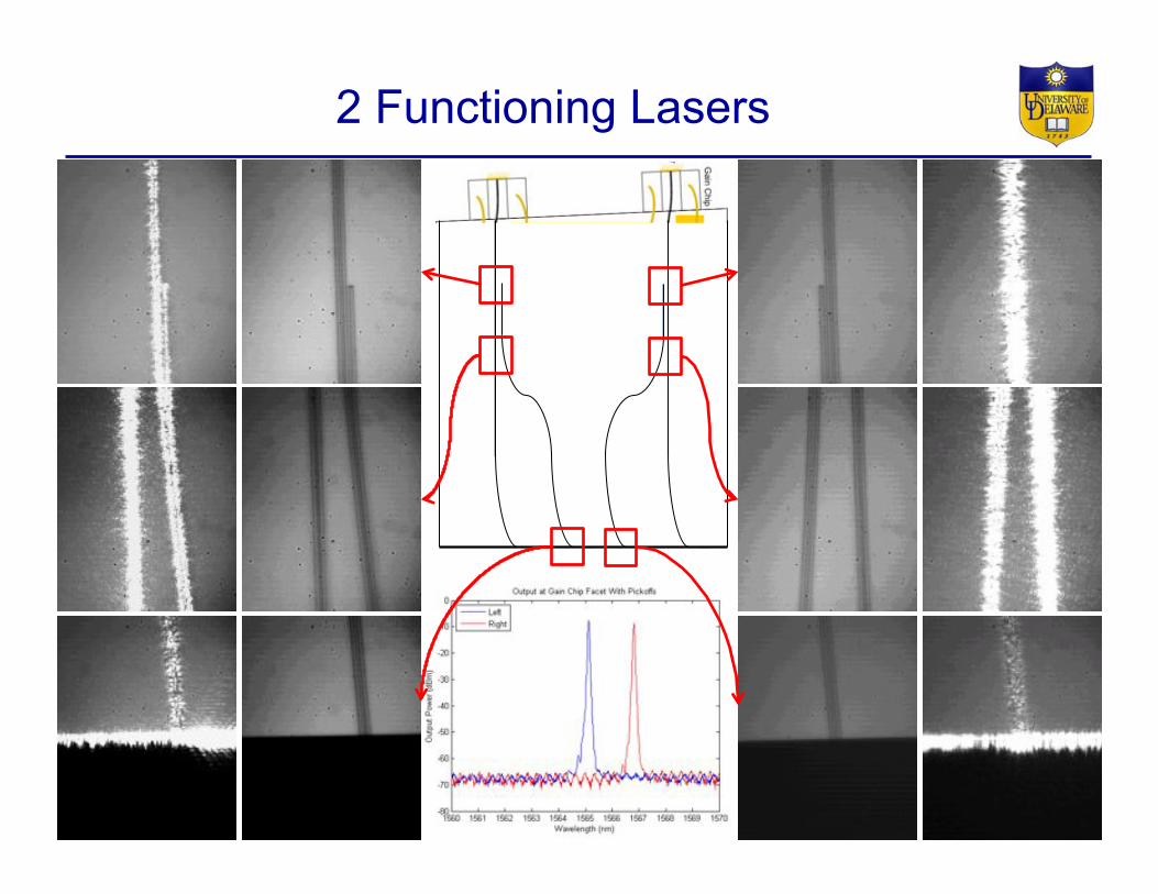
2 Functioning Lasers

Two Lasers on a Chip
~0.45 nm ~55 GHz
Silicon Nanomembrane 3D Integration for RF Signal Routing
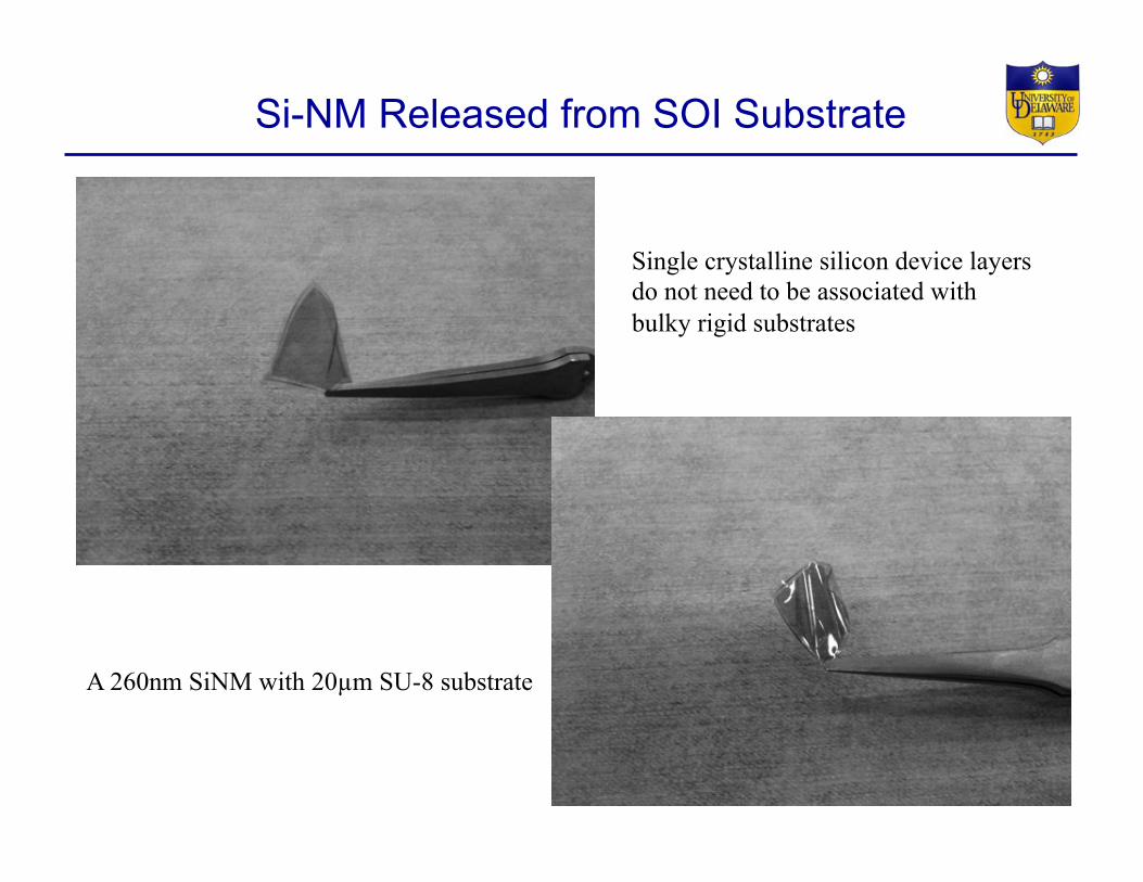
Si-NM Released from SOI Substrate
A 260nm SiNM with 20µm SU-8 substrate
Single crystalline silicon device layers do not need to be associated with bulky rigid substrates

WDM Si-NM Spectral Response
λ = 1550.0 nm λ = 1558.0 nm
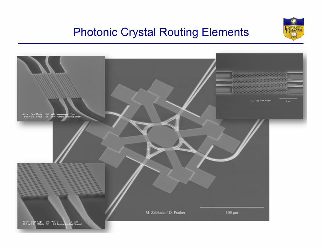
Photonic Crystal Routing Elements

8-Port Router!
A2 B2 A1 4 6 B1 6 4
A2 B2 A1 0 2mW B1 2mW 0
A2 B2 A1 0.16dB 0.24dB B1 0.24dB 0.16dB
Propaga'on)loss) Switching)Power)
Rou'ng)Table)
Switching)Table)
A2 B2 A1 0 2 B1 2 0
The switch voltage is 1.2V with 2mA of current

Testing at Texas A&M Univ. Cyclotron
Beam Line (Proton, N, Kr) http://cyclotron.tamu.edu/ref/data_room.php
• Dosage: 14N and 84Kr ions at15 MeV with 6x10⁶ ions/cm2 Flux with total doses of 20 krad • Minimal increase in current with set voltage exposed to LET radiation • ~ 1% decrease in current with set voltage during sample relaxation after ion beam removed

Summary
• Presented an overview of passive RF imaging and the driving
needs for advanced systems
• Discussed the realization of ultra high bandwidth optical phase
modulators
• Looked at the application of ultra-wideband RF frequency
synthesis and linear RF detection
• Discussed nanomembrane integration an RF signal router for
multi-functional RF systems
• Thank You!