Migration from MC55/MC56 to MC55i - GSM / GPRS · PDF fileMigration from MC55/MC56 to MC55i...
31
Migration Guide Migration from MC55/MC56 to MC55i Version: 02 DocID: MC55/MC56_MC55i_migration_v02n
Transcript of Migration from MC55/MC56 to MC55i - GSM / GPRS · PDF fileMigration from MC55/MC56 to MC55i...

Mig
ratio
n G
uide
Migration from MC55/MC56 to MC55i Version: 02 DocID: MC55/MC56_MC55i_migration_v02n

Migration from MC55/MC56 to MC55i Confidential / Released
MC55/MC56_MC55i_migration_v02n Page 2 of 31 2008-11-28
Document Name: Migration from MC55/MC56 to MC55i Version: 02 Date: November 28, 2008 DocId: MC55/MC56_MC55i_migration_v02n Status: Confidential / Released
GENERAL NOTE THE USE OF THE PRODUCT INCLUDING THE SOFTWARE AND DOCUMENTATION (THE "PRODUCT") IS SUBJECT TO THE RELEASE NOTE PROVIDED TOGETHER WITH PRODUCT. IN ANY EVENT THE PROVISIONS OF THE RELEASE NOTE SHALL PREVAIL. THIS DOCUMENT CONTAINS INFORMATION ON CINTERION PRODUCTS. THE SPECIFICATIONS IN THIS DOCUMENT ARE SUBJECT TO CHANGE AT CINTERION'S DISCRETION. CINTERION WIRELESS MODULES GMBH GRANTS A NON-EXCLUSIVE RIGHT TO USE THE PRODUCT. THE RECIPIENT SHALL NOT TRANSFER, COPY, MODIFY, TRANSLATE, REVERSE ENGINEER, CREATE DERIVATIVE WORKS; DISASSEMBLE OR DECOMPILE THE PRODUCT OR OTHERWISE USE THE PRODUCT EXCEPT AS SPECIFICALLY AUTHORIZED. THE PRODUCT AND THIS DOCUMENT ARE PROVIDED ON AN “AS IS” BASIS ONLY AND MAY CONTAIN DEFICIENCIES OR INADEQUACIES. TO THE MAXIMUM EXTENT PERMITTED BY APPLICABLE LAW, CINTERION WIRELESS MODULES GMBH DISCLAIMS ALL WARRANTIES AND LIABILITIES. THE RECIPIENT UNDERTAKES FOR AN UNLIMITED PERIOD OF TIME TO OBSERVE SECRECY REGARDING ANY INFORMATION AND DATA PROVIDED TO HIM IN THE CONTEXT OF THE DELIVERY OF THE PRODUCT. THIS GENERAL NOTE SHALL BE GOVERNED AND CONSTRUED ACCORDING TO GERMAN LAW. Copyright Transmittal, reproduction, dissemination and/or editing of this document as well as utilization of its contents and communication thereof to others without express authorization are prohibited. Offenders will be held liable for payment of damages. All rights created by patent grant or registration of a utility model or design patent are reserved. Copyright © 2008, Cinterion Wireless Modules GmbH Trademark notice Microsoft and Windows are either registered trademarks or trademarks of Microsoft Corporation in the United States and/or other countries.

Migration from MC55/MC56 to MC55i Confidential / Released
MC55/MC56_MC55i_migration_v02n Page 3 of 31 2008-11-28
Contents
0 Document History .........................................................................................................5
1 Introduction ...................................................................................................................6 1.1 Related Documents ...............................................................................................6 1.2 Type Approval........................................................................................................6
2 Hardware Related Differences .....................................................................................7 2.1 General Properties.................................................................................................7
2.1.1 Frequency Bands.....................................................................................7 2.1.2 Dimensions and Weight ...........................................................................8 2.1.3 Operating Temperature............................................................................9 2.1.4 TTY/CTM Support....................................................................................9 2.1.5 Operating Modes .....................................................................................9
2.2 Power-Up Behavior..............................................................................................10 2.3 Power-Down Behavior .........................................................................................11
2.3.1 Discharge at VDD Pin ............................................................................11 2.3.2 Switch off during Charge-only Mode......................................................12
2.4 Charging Application............................................................................................13 2.5 Application Interfaces ..........................................................................................14
2.5.1 SIM Interface..........................................................................................14 2.5.2 Audio Interface.......................................................................................14 2.5.2.1 DAI timing ..............................................................................................15 2.5.2.2 Audio programming model.....................................................................17 2.5.2.3 Characteristics of audio modes..............................................................18 2.5.2.4 Voiceband Receive Path........................................................................20 2.5.2.5 Reference Equipment for Type Approval...............................................21 2.5.3 Serial Interface.......................................................................................22 2.5.4 Control Signals.......................................................................................24
2.6 Electrical Characteristics .....................................................................................25 2.6.1 Signal Description..................................................................................25 2.6.2 Air Interface............................................................................................28
3 Software Related Differences ....................................................................................29 3.1 Firmware Update .................................................................................................29 3.2 Encryption Algorithms..........................................................................................29 3.3 Audio Interface.....................................................................................................29
3.3.1 Audio Loop Setting.................................................................................29 3.3.2 Internal CTM Modem .............................................................................29
3.4 Remote SAT (SIM Application Toolkit) ................................................................30 3.4.1 Interface Activation ................................................................................30 3.4.2 Remote SAT Get Information.................................................................30 3.4.3 Icon Handling.........................................................................................30
3.5 Support for Windows XP, Windows Vista, Windows Mobile 6 .............................31 3.6 Temperature Control............................................................................................31 3.7 Setting Escape Sequence Character (ATS2) ......................................................31 3.8 AT+CCLK Real Time Clock .................................................................................31

Migration from MC55/MC56 to MC55i Confidential / Released
MC55/MC56_MC55i_migration_v02n Page 4 of 31 2008-11-28
Tables Table 1: Frequency bands........................................................................................................7 Table 2: Operating temperatures .............................................................................................9 Table 3: TTY support................................................................................................................9 Table 4: SIM interface ............................................................................................................14 Table 5: DAI characteristics comparison................................................................................15 Table 6: Audio mode characteristics ......................................................................................18 Table 7: Default SNFO parameter..........................................................................................19 Table 8: Voiceband receive path............................................................................................20 Table 9: Electrical description of application interface ...........................................................25
Figures Figure 1: MC55i – top view.......................................................................................................8 Figure 2: MC55i startup..........................................................................................................10 Figure 3: Discharge at VDD pin..............................................................................................11 Figure 4: External circuit to switch off MC55i during charging. ..............................................12 Figure 5: Additional capacitor on DSB45 B1.1 .......................................................................13 Figure 6: Audio block diagram................................................................................................14 Figure 7: MC55i DAI timing ....................................................................................................15 Figure 8: DAI startup ..............................................................................................................16 Figure 9: AT audio programming model.................................................................................17 Figure 10: Reference equipment for MC55i type approval.....................................................21 Figure 11: ASC0 signal state differences between MC55/MC56 and MC55i.........................22 Figure 12: ASC1 signal state differences between MC55/MC56 and MC55i.........................23 Figure 13: SYNC and EMERGOFF upon startup...................................................................24

Migration from MC55/MC56 to MC55i Confidential / Released
MC55/MC56_MC55i_migration_v02n Page 5 of 31 2008-11-28
0 Document History
Preceding document: "Migration from MC55/MC56 to MC55i" Version 01 New document: "Migration from MC55/MC56 to MC55i" Version 02
Chapter What is new
-- Removed section on electrostatic discharge. ESD at antenna port has been measured to be the same as for MC55/MC56.
2.3.2 Revised complete section.
2.4 Added new section: Charging Application.
-- Removed section on antenna interface.
2.5.2.3 Updated audio mode characteristics.
3.6 Removed separate section “Deferred Shutdown”. Summary of new AT^SCTM parameters provided in Section 3.6 only.

Migration from MC55/MC56 to MC55i Confidential / Released
MC55/MC56_MC55i_migration_v02n Page 6 of 31 2008-11-28
1 Introduction
This migration document1 compares the Cinterion wireless modules MC55/MC56 and MC55i and lists hardware as well as software related differences between the modules. The aim of the document is to provide information and to offer support in order to facilitate the migration from MC55/MC56 to MC55i.
1.1 Related Documents
[1] MC55/MC56 Hardware Interface Description [2] MC55i Hardware Interface Description [3] MC55/MC56 AT Command Set [4] MC55i AT Command Set [5] DSB45 Development Support Box [6] Remote-SAT User’s Guide for MC55i [7] Application Note 02: Audiio Interface Design for GSM Applications [8] Application Note 23: DSB45 Installation for MC55i
1.2 Type Approval
MC55/MC56 and MC55i comply with the same standards and directives.
1 The document is effective only if listed in the appropriate Release Notes as part of the technical documentation delivered with your Cinterion wireless product.
Migration from MC55/MC56 to MC55i Confidential / Released
MC55/MC56_MC55i_migration_v02n Page 7 of 31 2008-11-28
2 Hardware Related Differences
This chapter comprises hardware related differences between MC55/MC56 and MC55i. It also refers to sections of the MC55/MC56 Hardware Interface Description [1] describing features and properties that were modified for MC55i.
2.1 General Properties
This section lists general properties that were modified for MC55i compared to MC55/MC56.
2.1.1 Frequency Bands
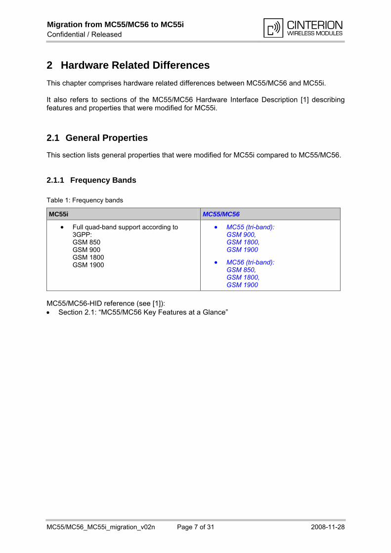
Table 1: Frequency bands
MC55i MC55/MC56
Full quad-band support according to 3GPP: GSM 850 GSM 900 GSM 1800 GSM 1900
MC55 (tri-band): GSM 900, GSM 1800, GSM 1900
MC56 (tri-band): GSM 850, GSM 1800, GSM 1900
MC55/MC56-HID reference (see [1]): Section 2.1: “MC55/MC56 Key Features at a Glance”
Migration from MC55/MC56 to MC55i Confidential / Released
MC55/MC56_MC55i_migration_v02n Page 8 of 31 2008-11-28
2.1.2 Dimensions and Weight
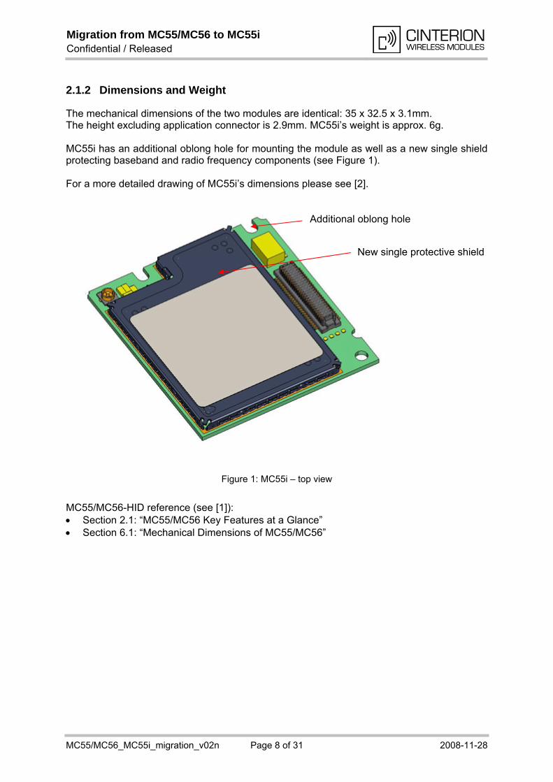
The mechanical dimensions of the two modules are identical: 35 x 32.5 x 3.1mm. The height excluding application connector is 2.9mm. MC55i’s weight is approx. 6g. MC55i has an additional oblong hole for mounting the module as well as a new single shield protecting baseband and radio frequency components (see Figure 1). For a more detailed drawing of MC55i’s dimensions please see [2].
Figure 1: MC55i – top view
MC55/MC56-HID reference (see [1]): Section 2.1: “MC55/MC56 Key Features at a Glance” Section 6.1: “Mechanical Dimensions of MC55/MC56”
Additional oblong hole
New single protective shield

Migration from MC55/MC56 to MC55i Confidential / Released
MC55/MC56_MC55i_migration_v02n Page 9 of 31 2008-11-28
2.1.3 Operating Temperature
The operating temperatures for both modules are listed in the below table.
Table 2: Operating temperatures
MC55i MC55/MC56 Parameter Unit
Min Typ Max Min Typ Max
Ambient temperature (according to GSM 11.10)
°C -20 +25 +55 -20 +25 +55
Restricted operation °C -40 to -20
+55 to +70 -25 to -20 +55 to +70
Automatic shutdown
Module temperature
Battery temperature
°C
-40
-20
+70
+60
-25
-18
+70
+60
Charging temperature (software controlled fast charging)
°C 0 +45 0 +45
It is possible to mount a heat sink at the bottom side of MC55i. MC55/MC56-HID reference (see [1]): Section 2.1: “MC55/MC56 Key Features at a Glance” Section 5.2: “Operating Temperatures”
2.1.4 TTY/CTM Support
Table 3: TTY support
MC55i MC55/MC56
CTM equipment can be connected to one of the three audio interfaces.
In addition, MC55i supports an internal TTY/CTM-Modem. TTY equipment can therefore be connected directly to one of the three audio interfaces (see also Section 3.3.2).
CTM equipment can be connected to one of the three audio interfaces.
2.1.5 Operating Modes
With MC55i a direct transition between Charge-only mode and ALARM mode is no longer possible. An indirect state transition via other modes is available – for details see [2]. MC55/MC56-HID reference (see [1]): Section 3.7: “Summary of State Transitions (except SLEEP mode)”
Migration from MC55/MC56 to MC55i Confidential / Released
MC55/MC56_MC55i_migration_v02n Page 10 of 31 2008-11-28
2.2 Power-Up Behavior
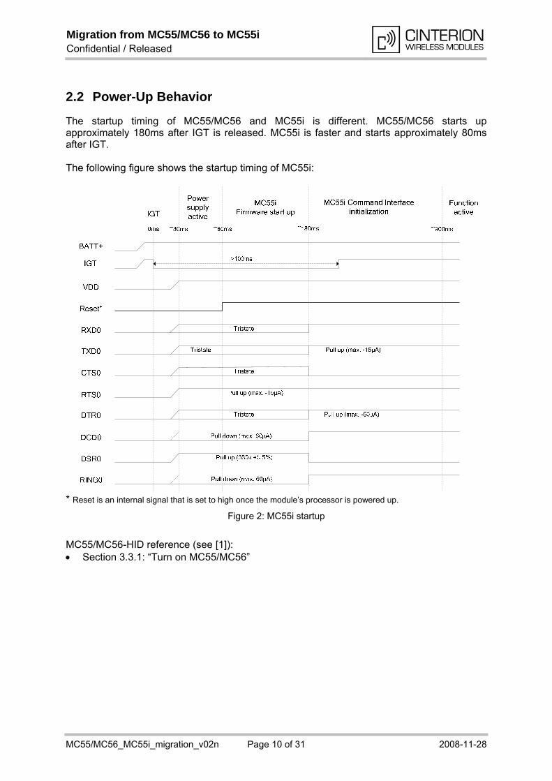
The startup timing of MC55/MC56 and MC55i is different. MC55/MC56 starts up approximately 180ms after IGT is released. MC55i is faster and starts approximately 80ms after IGT. The following figure shows the startup timing of MC55i:
* Reset is an internal signal that is set to high once the module’s processor is powered up.
C55/MC56-HID reference (see [1]):
6”
Figure 2: MC55i startup
M Section 3.3.1: “Turn on MC55/MC5

Migration from MC55/MC56 to MC55i Confidential / Released
MC55/MC56_MC55i_migration_v02n Page 11 of 31 2008-11-28
2.3 Power-Down Behavior
The switch off timing varies between MC55/MC56 and MC55i. The switch off time for MC55/MC56 ranges from immediately to about 3.2s. MC55i is always powered off immediately, even for a hardware driven emergency shutdown using the EMERGOFF (Power Down) line. MC55/MC56-HID reference (see [1]): Section 3.3.2: “Turn off MC55/MC56” Section 3.7: “Summary of State Transitions (Except SLEEP Mode)”
2.3.1 Discharge at VDD Pin
On switching off MC55i, the discharge at the external voltage supply pin VDD requires more time than with MC55/MC56. The varying VDD behavior is shown in the below figure.
Figure 3: Discharge at VDD pin
Please note that because of this behavior the serial interface drivers on the development Support Board DSB45 react in a way that the modem status lines will stay in an active state, even if the MC55i itself is switched off.

Migration from MC55/MC56 to MC55i Confidential / Released
MC55/MC56_MC55i_migration_v02n Page 12 of 31 2008-11-28
2.3.2 Switch off during Charge-only Mode
To switch off MC55i during Charge-only mode an external circuit will have to be implemented at the module’s charging interface as shown in the figure below:
100
k47
0k10
0n
100k
470k
47k
Figure 4: External circuit to switch off MC55i during charging.
lternatively, the charger has to be disconnected, i.e., the charging interface’s POWER A
signal has to be set to low, in order to switch the module off during Charge-only mode.

Migration from MC55/MC56 to MC55i Confidential / Released
MC55/MC56_MC55i_migration_v02n Page 13 of 31 2008-11-28
2.4 Charging Application
In order to employ a sine half-wave charger for MC55i that generates a pulsating DC voltage it is necessary to insert a 47µF 25V capacitor between the charger and the module’s POWER line. The DSB45 Support Board Revision B1.2 has an appropriate capacitor and can be used with MC55i as described in [5] and [8]. The following figure shows how to mount such a 47µF capacitor on a DSB45 Support Board B1.1.
Figure 5: Additional capacitor on DSB45 B1.1
Because of this modification the sample application given in the MC55i-HID has been adapted. It now shows the 47µF 25V capacitor instead of the 100nF capacitor recommended for MC55/MC56 on the connection between the charger and the POWER pin. Replacing the capacitor has no effect on MC55/MC56 applications. MC55/MC56-HID reference (see [1]): Chapter 8: “Design Example”
Migration from MC55/MC56 to MC55i Confidential / Released
MC55/MC56_MC55i_migration_v02n Page 14 of 31 2008-11-28
2.5 Application Interfaces
This section lists differences between the application interfaces of MC55/MC56 and MC55i.
2.5.1 SIM Interface
Table 4: SIM interface
MC55i MC55/MC56
Supported SIM cards: 3V 1.8V
Supported SIM card: 3V
MC55/MC56-HID reference (see [1]): Section 2.1: “MC55/MC56 Key Features at a Glance” Section 3.11: “SIM interface”
2.5.2 Audio Interface
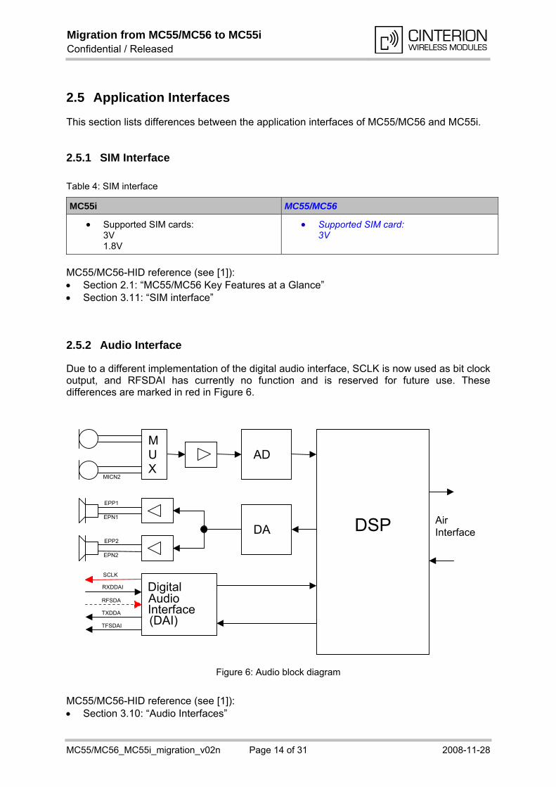
Due to a different implementation of the digital audio interface, SCLK is now used as bit clock output, and RFSDAI has currently no function and is reserved for future use. These differences are marked in red in Figure 6.
Figure 6: Audio block diagram
MC55/MC56-HID reference (see [1]): Section 3.10: “Audio Interfaces”
M U X
AD
DSP DA
Air Interface
Digital Audio Interface (DAI)
MICN2
EPP1
EPN1
EPP2
EPN2
SCLK RXDDAI
TFSDAI
RFSDA TXDDA
Migration from MC55/MC56 to MC55i Confidential / Released
MC55/MC56_MC55i_migration_v02n Page 15 of 31 2008-11-28
2.5.2.1 DAI timing
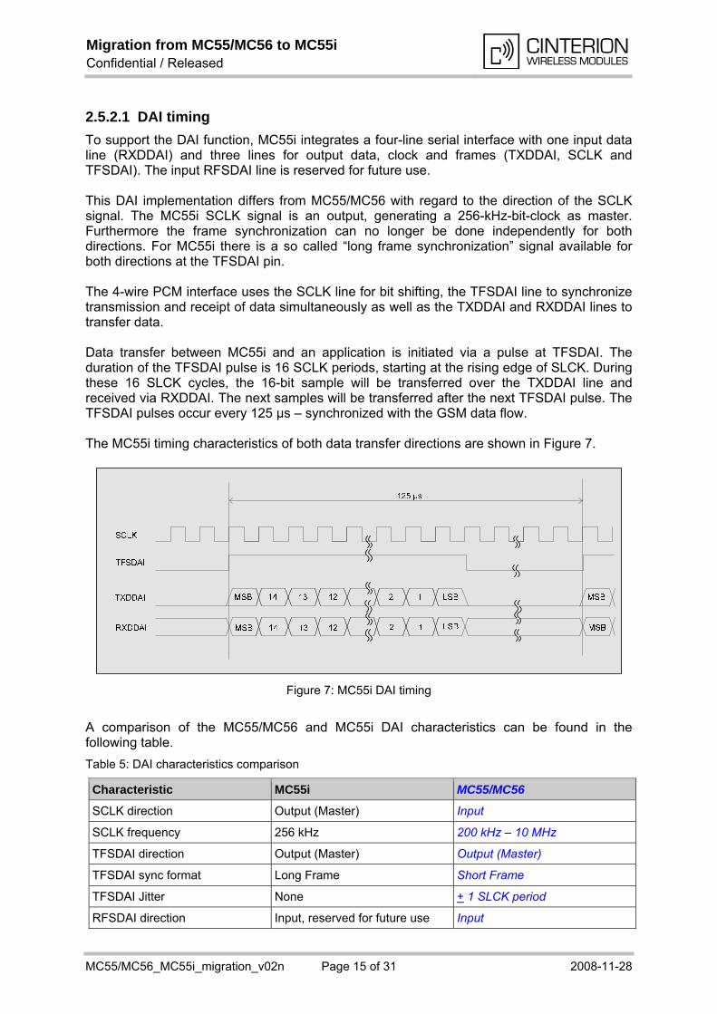
To support the DAI function, MC55i integrates a four-line serial interface with one input data line (RXDDAI) and three lines for output data, clock and frames (TXDDAI, SCLK and TFSDAI). The input RFSDAI line is reserved for future use. This DAI implementation differs from MC55/MC56 with regard to the direction of the SCLK signal. The MC55i SCLK signal is an output, generating a 256-kHz-bit-clock as master. Furthermore the frame synchronization can no longer be done independently for both directions. For MC55i there is a so called “long frame synchronization” signal available for both directions at the TFSDAI pin. The 4-wire PCM interface uses the SCLK line for bit shifting, the TFSDAI line to synchronize transmission and receipt of data simultaneously as well as the TXDDAI and RXDDAI lines to transfer data. Data transfer between MC55i and an application is initiated via a pulse at TFSDAI. The duration of the TFSDAI pulse is 16 SCLK periods, starting at the rising edge of SLCK. During these 16 SLCK cycles, the 16-bit sample will be transferred over the TXDDAI line and received via RXDDAI. The next samples will be transferred after the next TFSDAI pulse. The TFSDAI pulses occur every 125 µs – synchronized with the GSM data flow. The MC55i timing characteristics of both data transfer directions are shown in Figure 7.
Figure 7: MC55i DAI timing
A comparison of the MC55/MC56 and MC55i DAI characteristics can be found in the following table.
Table 5: DAI characteristics comparison
Characteristic MC55i MC55/MC56
SCLK direction Output (Master) Input
SCLK frequency 256 kHz 200 kHz – 10 MHz
TFSDAI direction Output (Master) Output (Master)
TFSDAI sync format Long Frame Short Frame
TFSDAI Jitter None + 1 SLCK period
RFSDAI direction Input, reserved for future use Input
Migration from MC55/MC56 to MC55i Confidential / Released
MC55/MC56_MC55i_migration_v02n Page 16 of 31 2008-11-28
Characteristic MC55i MC55/MC56
RFSDAI sync format n/a Short Frame
RFSDAI to TFSDAI delay not possible, both directions are transferred simultaneously
up to 100 µs
Data format 16 bit, linear, MSB first 16 bit, linear, MSB first
Data shifted out with rising edge rising edge
Data sampled in with falling edge falling edge
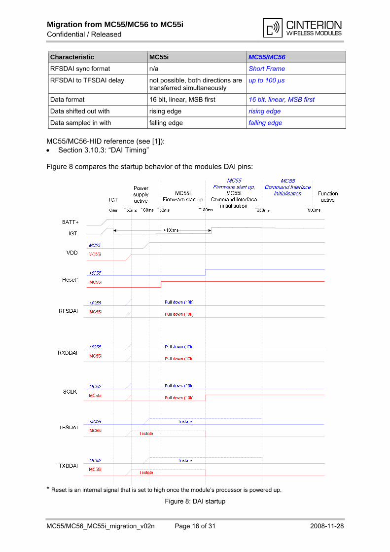
MC55/MC56-HID reference (see [1]): Section 3.10.3: “DAI Timing” Figure 8 compares the startup behavior of the modules DAI pins:
* Reset is an internal signal that is set to high once the module’s processor is powered up.
Figure 8: DAI startup
Migration from MC55/MC56 to MC55i Confidential / Released
MC55/MC56_MC55i_migration_v02n Page 17 of 31 2008-11-28
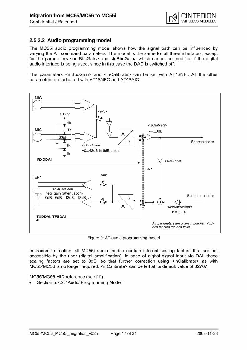
2.5.2.2 Audio programming model
The MC55i audio programming model shows how the signal path can be influenced by varying the AT command parameters. The model is the same for all three interfaces, except for the parameters <outBbcGain> and <inBbcGain> which cannot be modified if the digital audio interface is being used, since in this case the DAC is switched off. The parameters <inBbcGain> and <inCalibrate> can be set with AT^SNFI. All the other parameters are adjusted with AT^SNFO and AT^SAIC.
Figure 9: AT audio programming model
In transmit direction; all MC55i audio modes contain internal scaling factors that are not accessible by the user (digital amplification). In case of digital signal input via DAI, these scaling factors are set to 0dB, so that further correction using <inCalibrate> as with MC55/MC56 is no longer required. <inCalibrate> can be left at its default value of 32767. MC55/MC56-HID reference (see [1]): Section 5.7.2: “Audio Programming Model”
A
D
A
D
-...0dB
Speech coder
neg. gain (attenuation) 0dB, -6dB, -12dB, -18dB
+0...42dB in 6dB steps
1k
1k
1k
1k
2.65V
33u F
+
<sideTone>
AT parameters are given in brackets <…> and marked red and italic.
<outCalibrate[n]> n = 0...4
<inCalibrate>
<inBbcGain>
<outBbcGain>
Speech decoder
MIC
TXDDAI, TFSDAI
RXDDAI
<io>
<ep>
<mic>
EP1
EP2
MIC

Migration from MC55/MC56 to MC55i Confidential / Released
MC55/MC56_MC55i_migration_v02n Page 18 of 31 2008-11-28
2.5.2.3 Characteristics of audio modes
MC55i provides a new audio architecture and audio hardware. Due to the higher quality of the new audio hardware it is not longer necessary to improve for example some noise and linearity characteristics using limiters, compressors or AGC. MC55i therefore does not need these audio functions and they are not implemented. For MC55i, the echo suppression function of MC55/MC56 in some audio modes is replaced by a more suitable echo cancellation algorithm, providing for a better echo loss figure. Please note that the settings for the MC55/MC56 audio parameter blocks are incompatible with MC55i. Wherever necessary new parameter sets will have to be generated and imported. Nevertheless the audible characteristics of each audio mode of MC55i are more or less the same compared to MC55/MC56. The following table shows the characteristics of the MC55i audio modes. MC55/MC56 values that differ from MC55i values are shown in italics (and blue).
Table 6: Audio mode characteristics
Audio mode no. AT^SNFS=
1 (Default settings, not adjustable)
2 3 4 5 6
Name Default Handset
Basic Handsfree
Headset User Handset
Plain Codec 1
Plain Codec 2
Purpose DSB with Votronic handset
Car Kit Portable Headset DSB with individual handset
Direct access to speech coder
Direct access to speech coder
Gain setting via AT command. Defaults:
Fix
Adjustable
Adjustable
Adjustable
Adjustable
Adjustable
inBbcGain 4 (24dB) 2 (12dB) 6 (36dB)
5 (30dB)
4 (24dB) 0 (0dB) 0 (0dB)
outBbcGain 0 (6dB)
1 (-6dB)
2 (-12dB)
1 (-6dB)
2 (-12dB)
2 (-12dB)
0 (0dB)
1 (-6dB)
0 (0dB) 0 (0dB)
Default audio interface
1 2 2 1 1 2
Power supply ON (2.65V) ON (2.65V) ON (2.65V) ON (2.65V) ON (2.65V)
OFF (GND)
ON (2.65V)
OFF (GND)
Sidetone ON --- Adjustable Adjustable Adjustable Adjustable
Volume control OFF Adjustable Adjustable Adjustable Adjustable Adjustable
Limiter (receive) --- ON --- ON --- ON --- ON --- ---
Compressor (receive)
--- --- OFF --- --- --- ---
AGC (send) --- --- --- ON --- --- ---
Migration from MC55/MC56 to MC55i Confidential / Released
MC55/MC56_MC55i_migration_v02n Page 19 of 31 2008-11-28
Audio mode no. AT^SNFS=
1 (Default settings, not adjustable)
2 3 4 5 6
Echo control (send)
Cancellation
Suppression
Cancellation
Cancellation Suppression
Cancellation
---
Cancellation
Suppression
--- ---
Noise suppression --- 15dB
up to 10dB
15dB
10dB
--- --- ---
MIC input signal for 0dBm0 @ 1024 Hz (default gain)
18mV
23mV
65mV
58mV
7.5mV
7.5mV @ -3dBm0 due to AGC
18mV
23mV
315mV 315mV
EP output signal in mV rms. @ 0dBm0, 1024 Hz, no load (default gain); @ 3.14 dBm0
620mV 284mV
210mV 120mV default @ max volume
320mV 300mV default @ max volume
620mV 284mV default @ max volume
880mV 895mV
3.7Vpp
880mV 895mV
3.7Vpp
Sidetone gain at default settings
21.5dB
22.8dB
-∞ dB 20.5dB
Affected by AGC, 13dB @ 7.5mV (MIC)
21.5dB
22.8dB
-3dB @ sidetone = 8192
-∞ dB
-3dB @ sidetone = 8192
-∞ dB
The AT^SNFO parameter settings also differ between MC55i and MC55/MC56. The following table shows the default parameters for both modules - MC55/MC56 values are shown in italics (and blue). Table 7: Default SNFO parameter
Audio mode Default SNFO parameters
1 0,16384,16384,16384,16384,16384,4,10752
1,16384,16384,16384,16384,16384,4,8192
2 2,4685,6301,8500,11205,15115,4,0
1,4685,6301,8500,11205,15115,4,0
3 2,1253,2452,4891,9759,16383,4,2048
2,1253,2452,4891,9759,16383,4,682
4 0,4096,5792,8192,11584,16384,4,10752
1,10337,11598,13014,14602,16384,4,8192
5 0,4096,5792,8192,11584,16384,4,0
0,16384,16384,16384,16384,16384,4,0
6 0,4096,5792,8192,11584,16384,4,0
0,16384,16384,16384,16384,16384,4,0
MC55/MC56-HID reference (see [1]): Section 5.7.3: “Characteristics of Audio Modes”

Migration from MC55/MC56 to MC55i Confidential / Released
MC55/MC56_MC55i_migration_v02n Page 20 of 31 2008-11-28
2.5.2.4 Voiceband Receive Path
Table 8: Voiceband receive path
Parameter Min Typ Max Unit Test condition / remark
MC55i: Differential load capacitance
100 pF from EPP1 to EPN1
MC55i: Differential load capacitance
2000 pF from EPP2 to EPN2
MC55/MC56: Differential load capacitance
1000 pF from EPPx to EPNx
MC55/MC56-HID reference (see [1]): Section 5.7.4: “Voiceband Receive Path”

Migration from MC55/MC56 to MC55i Confidential / Released
MC55/MC56_MC55i_migration_v02n Page 21 of 31 2008-11-28
2.5.2.5 Reference Equipment for Type Approval
No DAI-Box is necessary for MC55i. The GSM type approval DAI according to GSM 11.10 is not supported by MC55i. Acoustic type approval will be done via the air interface.
GSM enginePC
Power supply
SIM
Flex cableor
Adapter board
2x RS-232
DSB45
Handset
Antenna or 50 cable to system simulator
Antenna
Audio test system
Figure 10: Reference equipment for MC55i type approval
MC55/MC56-HID reference (see [1]): Section 7.1: “Reference Equipment for Type Approval”
Migration from MC55/MC56 to MC55i Confidential / Released
MC55/MC56_MC55i_migration_v02n Page 22 of 31 2008-11-28
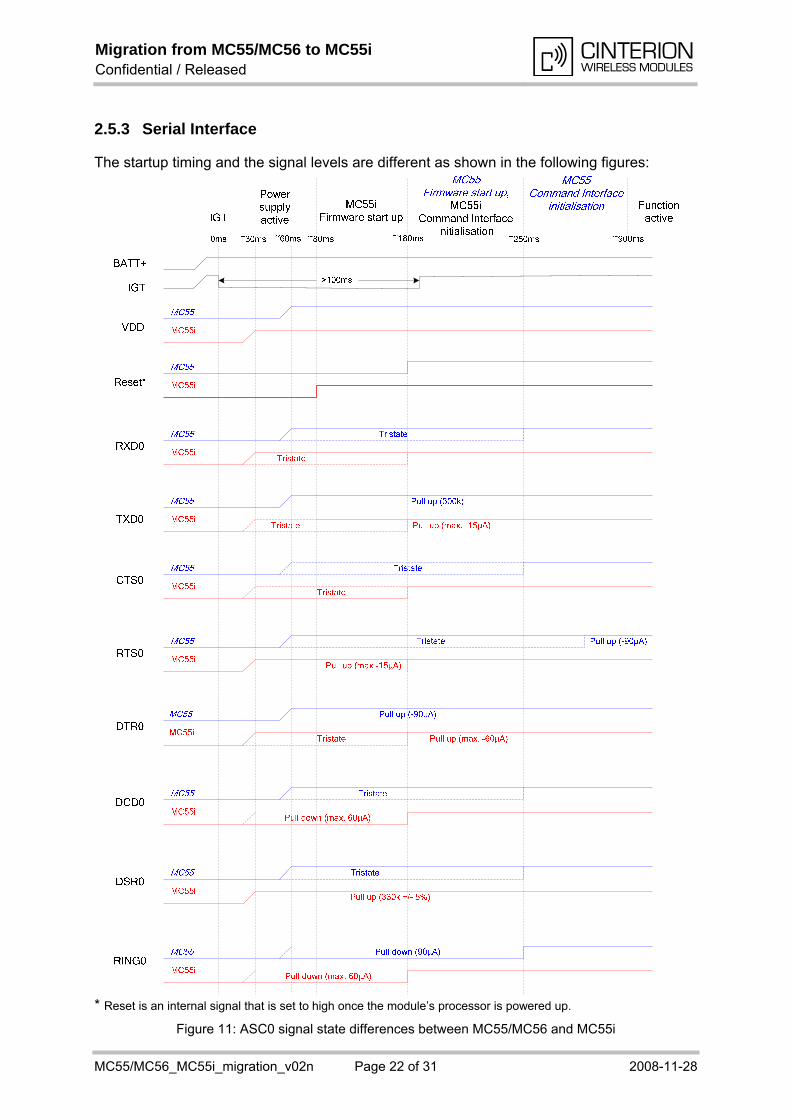
2.5.3 Serial Interface
The startup timing and the signal levels are different as shown in the following figures:
* Reset is an internal signal that is set to high once the module’s processor is powered up.
Figure 11: ASC0 signal state differences between MC55/MC56 and MC55i

Migration from MC55/MC56 to MC55i Confidential / Released
MC55/MC56_MC55i_migration_v02n Page 23 of 31 2008-11-28
RXD1
TXD1
CTS1
RTS1
Tristate
Tristate
Pull down (90µA), Pullup (-90µA) PU (-90µA)
Pull down (90µA), Pull up (-90µA) Pull up (-90µA)
Reset*
VDD
Pull down (max. 60µA) Pull up (max. -60µA)
Pull down (max. 300µA)
Tristate
Pull up (max. -60µA)
BATT+
IGT
Power supplyactive
,MC55i
Command Interface initialisation
FunctionactiveIGT
MC55iFirmware start up
~30ms0ms ~60ms ~80ms ~180ms ~250ms ~900ms
>100ms
MC55i
MC55i
MC55i
MC55i
MC55i
MC55i
* Reset is an internal signal that is set to high once the module’s processor is powered up.
Figure 12: ASC1 signal state differences between MC55/MC56 and MC55i
MC55/MC56-HID reference (see [1]): Section 3.3.1.1: “Turn on MC55/MC56 using the ignition line /IGT (Power on)” Section 3.9: “Serial Interfaces”
Migration from MC55/MC56 to MC55i Confidential / Released
MC55/MC56_MC55i_migration_v02n Page 24 of 31 2008-11-28
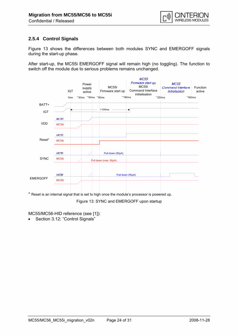
2.5.4 Control Signals
Figure 13 shows the differences between both modules SYNC and EMERGOFF signals during the start-up phase. After start-up, the MC55i EMERGOFF signal will remain high (no toggling). The function to switch off the module due to serious problems remains unchanged.
SYNC
EMERGOFF
Pull down (90µA)
Pull down (90µA)
Pull down (max. 60µA)
Reset*
VDD
BATT+
IGT
Power supplyactive
,MC55i
Command Interface initialisation
FunctionactiveIGT
MC55iFirmware start up
~30ms0ms ~60ms ~80ms ~180ms ~250ms ~900ms
>100ms
MC55i
MC55i
MC55i
MC55i
* Reset is an internal signal that is set to high once the module’s processor is powered up.
Figure 13: SYNC and EMERGOFF upon startup
MC55/MC56-HID reference (see [1]): Section 3.12: “Control Signals”

Migration from MC55/MC56 to MC55i Confidential / Released
MC55/MC56_MC55i_migration_v02n Page 25 of 31 2008-11-28
2.6 Electrical Characteristics
This section lists differences in the modules’ electrical characteristics.
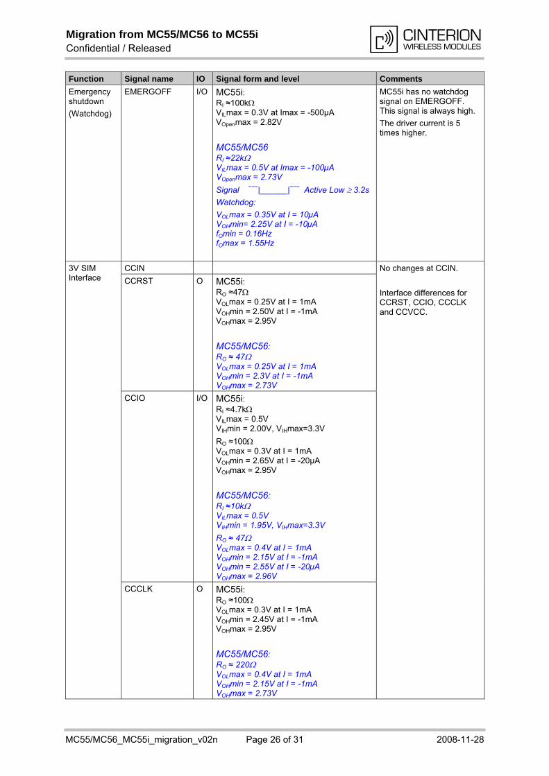
2.6.1 Signal Description
The differences in the characteristics of the electrical signals between both modules are described in the following table.
Table 9: Electrical description of application interface
Function Signal name IO Signal form and level Comments
POWER I MC55i VImin = 3.5V VImax = 12V
MC55/MC56 VImin = 3.0V VImax = 15V
Maximum input voltage reduced.
Charge interface
CHARGE O MC55i: ICHARGEmax = 2mA VIHmax = 12V VLOmax = 0.25V at I = 2mA
MC55/MC56: ICHARGE = 300µA ...-600µA @ 3V < VCHARGE < VLOAD
Changed from current sink to open collector.
External supply voltage
VDD O MC55i: VDDmin = 2.75V, VDDtyp= 2.85V, VDDmax = 2.95V
MC55/MC56: VDDmin = 2.84V, VDDtyp= 2.9V, VDDmax = 2.96V
Imax = -10mA CLmax = 1µF
The minimum output voltage is reduced by about 100mV.
VDD Low Power
VDDLP In Power Down mode, VDDLP does not drive IGT to HiZ any more.
Ignition IGT I MC55i: VILmax = (BATT+) -0.5V at I = -5µA
VILmin = 0V at Imax = -50µA VOpenmax = 4.8V
MC55/MC56: VILmax = 0.5V at Imax = -20µA VOpenmax = 2.3V
RI ≈ 100k, CI ≈ 1nF ON ~~~|____|~~~ Active Low 100ms
The maximum output voltage is higher and therefore the current has also changed.
The line must be driven low by an Open Drain or Open Collector driver.
Migration from MC55/MC56 to MC55i Confidential / Released
MC55/MC56_MC55i_migration_v02n Page 26 of 31 2008-11-28
Function Signal name IO Signal form and level Comments
Emergency shutdown
(Watchdog)
EMERGOFF I/O MC55i: RI ≈100k VILmax = 0.3V at Imax = -500µA VOpenmax = 2.82V
MC55/MC56 RI ≈22k VILmax = 0.5V at Imax = -100µA VOpenmax = 2.73V
Signal ~~~|______|~~~ Active Low 3.2s
Watchdog:
VOLmax = 0.35V at I = 10µA VOHmin= 2.25V at I = -10µA fOmin = 0.16Hz fOmax = 1.55Hz
MC55i has no watchdog signal on EMERGOFF. This signal is always high.
The driver current is 5 times higher.
CCIN
CCRST O MC55i: RO ≈47 VOLmax = 0.25V at I = 1mA VOHmin = 2.50V at I = -1mA VOHmax = 2.95V
MC55/MC56: RO ≈ 47 VOLmax = 0.25V at I = 1mA VOHmin = 2.3V at I = -1mA VOHmax = 2.73V
CCIO I/O MC55i: RI ≈4.7k VILmax = 0.5V VIHmin = 2.00V, VIHmax=3.3V
RO ≈100 VOLmax = 0.3V at I = 1mA VOHmin = 2.65V at I = -20µA VOHmax = 2.95V
MC55/MC56: RI ≈10k VILmax = 0.5V VIHmin = 1.95V, VIHmax=3.3V
RO ≈ 47 VOLmax = 0.4V at I = 1mA VOHmin = 2.15V at I = -1mA VOHmin = 2.55V at I = -20µA VOHmax = 2.96V
3V SIM Interface
CCCLK O MC55i: RO ≈100 VOLmax = 0.3V at I = 1mA VOHmin = 2.45V at I = -1mA VOHmax = 2.95V
MC55/MC56: RO ≈ 220 VOLmax = 0.4V at I = 1mA VOHmin = 2.15V at I = -1mA VOHmax = 2.73V
No changes at CCIN.
Interface differences for CCRST, CCIO, CCCLK and CCVCC.

Migration from MC55/MC56 to MC55i Confidential / Released
MC55/MC56_MC55i_migration_v02n Page 27 of 31 2008-11-28
Function Signal name IO Signal form and level Comments
CCVCC O MC55i: ROmax ≈ 5 CCVCCmin = 2.75V, CCVCCmax = 2.95V Imax = 20mA
MC55/MC56: ROmax = 5 CCVCCmin = 2.84V, CCVCCmax = 2.96V Imax = -20mA
CCGND Ground
CCIN I RI ≈ 100k VILmax = 0.5V VIHmin = 2.15V at I = 20µA, VIHmax=3.3V at I = 30µA
CCRST O RO ≈47 VOLmax = 0.25V at I = 1mA VOHmin = 1.40V at I = -1mA VOHmax = 1.95V
CCIO IO RI ≈4.7k VILmax = 0.3V VIHmin = 1.20V, VIHmax=3.3V
RO ≈100 VOLmax = 0.3V at I = 1mA VOHmin = 1.60V at I = -20µA VOHmax = 1.95V
CCCLK O RO ≈100 VOLmax = 0.3V at I = 1mA VOHmin = 1.40V at I = -1mA VOHmax = 1.95V
CCVCC O ROmax ≈ 5 CCVCCmin = 1.71V, CCVCCmax = 1.95V Imax = 20mA
1.8V SIM Interface
CCGND Ground
1.8V SIM Interface is new for MC55i.
RXD0 O
TXD0 I
CTS0 O
RTS0 I
DTR0 I
DCD0 O
DSR0 O
ASC0 interface
RING0 O
MC55i: VOLmax = 0.2V at I = 1mA VOHmin = 2.40V at I = -1mA VOHmax = 2.82V
VILmax = 0.5V VIHmin = 2.00V, VIHmax=3.3V
MC55/MC56: VOLmax = 0.2V at I = 1mA VOHmin = 2.35V at I = -1mA VOHmax = 2.73V
VILmax = 0.5V VIHmin = 1.95V, VIHmax=3.3V
DTR0, RTS0: Imax = -90µA at VIN = 0V
TXD0: Imax = -30µA at VIN = 0V
TXD0, RTS0: pull up -15µA at 0V
DTR0: pull up -60µA at 0V

Migration from MC55/MC56 to MC55i Confidential / Released
MC55/MC56_MC55i_migration_v02n Page 28 of 31 2008-11-28
Function Signal name IO Signal form and level Comments
RXD1 O
TXD1 I
CTS1 O
ASC1 interface
RTS1 I
MC55i: VOLmax = 0.2V at I = 1mA VOHmin = 2.40V at I = -1mA VOHmax = 2.82V
VILmax = 0.5V VIHmin = 2.00V, VIHmax=3.3V
MC55/MC56: VOLmax = 0.2V at I = 1mA VOHmin = 2.35V at I = -1mA VOHmax = 2.73V
VILmax = 0.5V VIHmin = 1.95V, VIHmax=3.3V
IImax = -90µA at VIN = 0V
TXD1, RTS1: pull up -60µA at 0V
RFSDAI I
RXDDAI I
SCLK O
I
TFSDAI O
Digital audio interface
TXDDAI O
MC55i: VOLmax = 0.2V at I = 1mA VOHmin = 2.40V at I = -1mA VOHmax = 2.82V
VILmax = 0.5V VIHmin = 2.00V, VIHmax=3.3V
MC55/MC56: VOLmax = 0.2V at I = 1mA VOHmin = 2.35V at I = -1mA VOHmax = 2.73V
VILmax = 0.5V VIHmin = 1.95V, VIHmax=3.3V IImax = 330µA at VIN = 3.3V
This interface has a changed functionality.
RFSDAI, RXDDAI, SCLK: pull down +330µA at VIN = 3.3V
MC55/MC56-HID reference (see [1]): Section 5.5: “Electrical Specifications of the Application Interface”
2.6.2 Air Interface
MC55i has improved receiver input sensitivity values:
Parameter Min Typ Max Unit
GSM 850 -102 -107*) dBm
EGSM 900 -102 -107*) dBm
GSM 1800 -102 -107*) MC55: -106
dBm
Receiver input sensitivity @ ARP
BER Class II < 2.4% (static input level)
GSM 1900 -102 -107*) MC55: -105.5
dBm
*) Typical value is at least -107dBm. MC55/MC56-HID reference (see [1]): Section 5.8: “Air Interface”

Migration from MC55/MC56 to MC55i Confidential / Released
MC55/MC56_MC55i_migration_v02n Page 29 of 31 2008-11-28
3 Software Related Differences
This chapter comprises software related differences between MC55/MC56 and MC55i.
3.1 Firmware Update
The SIM Swup feature available for MC55/MC56 is no longer supported for MC55i.
3.2 Encryption Algorithms
MC55i employs the A5/1 encryption algorithm. The A5/2 encryption algorithm is no longer supported.
3.3 Audio Interface
3.3.1 Audio Loop Setting
The new AT^SCFG parameter “Audio/Loop” has been introduced to configure an audio loop which can be used to simplify the verification of audio connections. The intention of this audio loop is for testing only at an implementer’s production facility. Full audio processing will be performed. Audio parameterization capabilities remain nearly unrestricted. Microphone and loudspeaker ports can be selected with random access. The audio loop cannot be used in combination with the digital audio interface. Neither a SIM card nor a GSM network is necessary to turn the audio loop on. For details on the AT command AT^SCFG and “Audio/Loop” see [4].
3.3.2 Internal CTM Modem
MC55i incorporates an internal CTM modem. The AT^SNFTTY parameter <audioState> has been enhanced to activate the TTY/CTM mode for this internal CTM modem. For details on the AT command AT^SNFTTY see [4].
Migration from MC55/MC56 to MC55i Confidential / Released
MC55/MC56_MC55i_migration_v02n Page 30 of 31 2008-11-28
3.4 Remote SAT (SIM Application Toolkit)
The Remote SAT interface has been changed as described in the following sections. For details please refer to [6].
3.4.1 Interface Activation
The Remote SAT interface activation via AT^SSTA is now able to switch between a default automatic response mode (AR Mode) and an explicit response mode (ER Mode). In AR mode (<mode>=0) all commands and responses are exchanged automatically
between the ME and the SIM application (default). This eliminates the need to enter any Remote SAT AT commands incl. the AT^SSTA command. If AR mode is enabled the ME enters the OFF state (<state>=1) after reboot.
ER mode (<mode>=1) is intended for use with an MMI. If ER mode is enabled the MMI is required to handle, via the module's Remote-SAT interface, all commands and responses transmitted to or from the SIM. If ER mode is enabled the ME enters the IDLE state (<state>= 2) after reboot.
3.4.2 Remote SAT Get Information
The command “AT^SSTGI Remote_Sat Get Information – Refresh (1) has been enhanced to support the new parameters <pathLen>,<fileNum>, <fileList>: AT^SSTGI=1 ^SSTGI: <cmdType>,<commandDetails>,<pathLen>,<fileNum>, <fileList> OK <pathLen>: Number of bytes coded in <fileList> <fileNum>: Number of updated Elementary Files (EF) with path given in <fileList> <fileList>: String containing Elementary File paths. This extra information enables the customer application to check which data files on the SIM/USIM have been changed and need to be read again. Doing so will prevent the application from working with outdated values.
3.4.3 Icon Handling
Several Remote SAT Proactive commands may provide an icon identifier. Icons are intended to enhance an MMI by providing graphical information to the user. The display of icons is optional for the ME. The SIM indicates to the ME whether the icon replaces an alpha identifier or text string, or whether it accompanies it (icon qualifier).
Migration from MC55/MC56 to MC55i Confidential / Released
MC55/MC56_MC55i_migration_v02n Page 31 of 31 2008-11-28
3.5 Support for Windows XP, Windows Vista, Windows Mobile 6
The MC55i modules supports Microsoft® Windows XP, Microsoft® Windows Vista™ and Windows Mobile® 6: Multiplexer and Modem drivers are provided for Windows XP and Windows Vista. New RIL and Multiplexer drivers are provided for Windows Mobile 6. If MC55/MC56 is
replaced by MC55i these drivers will also have to be replaced.
3.6 Temperature Control
The AT^SCTM command has been enhanced as follows: The additional parameters <p> of the AT^SCTM write command and <temp> of the
AT^SCTM? read command enable the MC55i module to display the exact board temperature in degrees Celsius.
Compared to MC55/MC56, the guard period for deferred shutdown has been extended from 15 seconds to 2 minutes after power-up.
For details on the AT command AT^SCTM see [2] and [4].
3.7 Setting Escape Sequence Character (ATS2)
With MC55i the AT command ATS2 has been implemented for V.250ter compatibility reasons. For details on the AT command ATS2 see [4].
3.8 AT+CCLK Real Time Clock
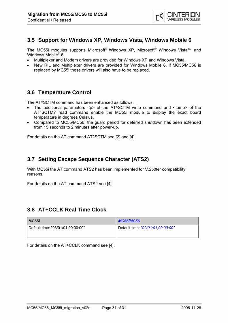
MC55i MC55/MC56
Default time: "03/01/01,00:00:00" Default time: "02/01/01,00:00:00"
For details on the AT+CCLK command see [4].