Midterm Exam 2 Signature:
11
EE143 Microfabrication Technology Spring 2011 Prof. J. Bokor Midterm Exam 2 Name: ---------------=~------------------------------- Signature: _ SID: _ CLOSED BOOK. TWO 8 1/2" X 11" SHEET OF NOTES, AND SCIENTIFIC POCKET CALCULATOR PERMITTED. MAKE SURE THE EXAM PAPER HAS l' PAGES. DO ALL WORK ON THE EXAM PAGES. USE THE BACK OF PAGES IF NECESSARY. TIME ALLOTTED: 80 MINUTES Fundamental constants you might need: Boltzmann's constant, k = 1.38 X 1O- 23 11K Permittivity of free space, 8 0 = 8.85 X 10- 12 Flm Permeability of free space, J..lo = 1.26 x 10- 6 Him Speed of light in vacuum, c = 2.998 x 10 8 mls Electron charge, e = 1.6 x 10- 19 C Free electron mass, IDa = 9.1 X 10- 31 kg Electron volt, 1 eV = 1.6 x 10- 19 1 Thermal voltage, kT/q = 0.0258 V (at 300K) Relative dielectric constant of silicon, K, = 11.8 Relative dielectric constant of silicon dioxide, K, = 3.9 Effective masses in silicon at 300K. Electrons: mn* = 1.18 IDa; Holes: mp* = 0.81 IDa I Silicon band gap at 300K, Eg= 1.12 eV 1
Transcript of Midterm Exam 2 Signature:
EE143 Microfabrication TechnologySpring 2011
Prof. J. Bokor
Midterm Exam 2
Name: ---------------=~-------------------------------Signature: _
SID: _
CLOSED BOOK. TWO 8 1/2" X 11" SHEET OF NOTES, AND SCIENTIFIC POCKETCALCULATOR PERMITTED. MAKE SURE THE EXAM PAPER HAS l'PAGES.DO ALL WORK ON THE EXAM PAGES. USE THE BACK OF PAGES IFNECESSARY.
TIME ALLOTTED: 80 MINUTES
Fundamental constants you might need:
Boltzmann's constant, k = 1.38 X 1O-2311K
Permittivity of free space, 80 = 8.85 X 10⁻¹² Flm
Permeability of free space, J..lo = 1.26 x 10⁻⁶ Him
Speed of light in vacuum, c = 2.998 x 10⁸ mls
Electron charge, e = 1.6 x 10⁻¹⁹ C
Free electron mass, IDa = 9.1 X 10⁻³¹ kg
Electron volt, 1 eV = 1.6 x 10⁻¹⁹ 1
Thermal voltage, kT/q = 0.0258 V (at 300K)
Relative dielectric constant of silicon, K, = 11.8
Relative dielectric constant of silicon dioxide, K, = 3.9
Effective masses in silicon at 300K. Electrons: mn* = 1.18 IDa; Holes: mp* = 0.81 IDa
I Silicon band gap at 300K, Eg= 1.12 eV
1

1. Thin Film Deposition (25 points)a. In the EE143 lab, we use a thermal evaporator to deposit the aluminum thin film.
Before the evaporation, a mechanical pump and turbo pump are used to lower thepressure of the chamber. (12 points)i) What is the purpose ofthis pumping step? (3 points)
IJ-e e\JO'.CvG.-te -f-k. ct·'-~L•....L e( fe evlsvr( +k+tk At aJoVlAj {'-allow $+,tf\cht t("~ec.-k,·(es ~k soocce -to -f-lAe. wd-Cer. '-Yf\ lov+ o..tA( co(liSlof'{~
LPI+~ Ioctckgro.,).J1°-s t'IAolec.J{e'S. We ~(5D tV~+ fc",fe-serve. i-l~ -.>r'tt, t>-P-+le. defos'(+e~+t(M.
ii) If the pressure of chamber P = 10-2 Torr, will the evaporation work well? Howabout P = 10-4torr? Explain. [Hint: Calculate the mean free path for molecularcollisions. Use a diameter of0.25nm for the Al atoms.] (6 points)
Y'Ae.u pree.. peL~~ ~ r c.o [h SC'OI't-S " eJ\'~'IMJa~ 5, z;e "\.0- /SC""1'A,CMM. J ==- O.o~I 'P (to ("f)
-2.. t \ -./a. oS-:p:::(0 0 rt: .....::;A, z: 10-i .::;S 1'\'\ IN\. «< ISCI/v\.
5~ +k~5 ~ e51\..\- ~o;' k. f.0e li~" r.::; 10-"',0(( ~ A z: () .o~ ..:::5'OfCV\A ------.lr~"L/Ito-tlf ./
"50 ~k~~Wo/~$ 0 kt Lowe/' pvessvretvovl~ b e ~ b-eUw
iii) After our thermal evaporation step, the metal layer will not be conformal.Why? What methods can be used to make it more conformal? (List at leastthree) (3 points)
-7 d.l (cc+-tt;:~~ £~OS'I +/~ ij 5.Jk; eel- 1-0 s h..-..J.o Wlv:J Co ~ dtl ~ A.O 1- Co tA.-90 \f Ma ...l .
t. R..o+l-~e ~. ~ll++4 ~1.)6$tr~le:2- I ra..~(se j ~ ~ ..;>"s+ra-fe +e~f~/~.:~,)( e~ use CL {~se-( 6..('~ SOJrce
2
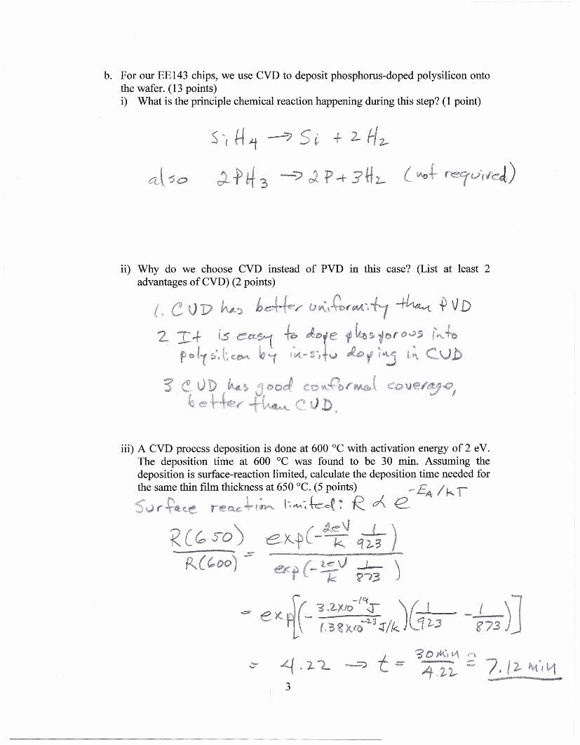
b. For our EE143 chips, we use CVD to deposit phosphorus-doped polysilicon ontothe wafer. ( 13 points)i) What is the principle chemical reaction happening during this step? (1 point)
s ~(Hi--==; 5~ + 2- H 2-
d- .f'~ 3 --'l 01P -+ .?«z, L v'O+ re'r '.i,,(cJ)
ii) Why do we choose CVD instead of PVD in this case? (List at least 2advantages ofCVD) (2 points)
t. C V D lv-:> b,;,.{-fe~u \~rM .•-ft ~ -P VD
z I+ is ea..~ ~ kte ~~s.!oro~, l~+epc'''( ~:LCC~ b'( ";1,,- s',f.v J.o f I~ L>\ C.VD
"S ~. U D b'-L~ t':j OQ& co "/'"'0 r~J\.W.l Co lJer~·".Q'/I 1. v ~"'I
il.'.l t!?~'l€"'" t l ~c. V
iii) A CVD process deposition is done at 600 DC with activation energy of 2 eV.The deposition time at 600 DC was found to be 30 min. Assuming thedeposition is surface-reaction limited, calculate the deposition time needed forthe same thin film thickness at 650 DC. (5 points) r-: Elk I5vr~tl.t- Q.e.~t· \~""-:~ ': R 0\ C. -4
C ~e\J -.L.)eKf -k: C(2,3
~~(_~V ..J- \• 1 ?i3 J
KC~ s-o ')~l'OO) ..::
{( -(~ )6 ~7JJ-= "3.2...'1-10 T Iex:· ... - t. '3 ~ >tlc)1.3 :.r!k: :12.-.:3
t '3'" #\1 V\ ("\.-- ~ .l-l.. -=:> - ... 7 f /2.- i\.t'/11.••.. 4·2..2-.. - •3

iv) Redo (iii) assuming the deposition is mass-transport limited. (5 points)
M <l?" +r1l<-L5 po ( +- t", vIA.", -I-R cA T?/L
c~i511- =- ;, 087
'30 II;{t II\.•
1,087
4
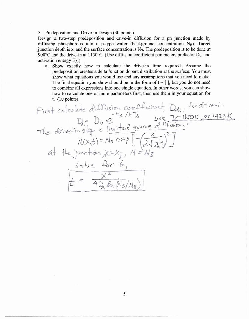
2. Predeposition and Drive-in Design (30 points)Design a two-step predeposition and drive-in diffusion for a pn junction made bydiffusing phosphorous into a p-type wafer (background concentration NB). Targetjunction depth is Xj and the surface concentration is Ns. The predeposition is to be done at900°C and the drive-in at 1150°C. (Use diffusion coefficient parameters prefactor Do, andactivation energy EA')
a. Show exactly how to calculate the drive-in time required. Assume thepredeposition creates a delta function dopant distribution at the surface. You mustshow what equations you would use and any assumptions that you need to make.The final equation you show should be in the form oft = [], but you do not needto combine all expressions into one single equation. In other words, you can showhow to calculate one or more parameters first, then use them in your equation fort. (10 points)
, (! e t t-.: tv: L f rJ. 0o,dr;ve-t'1/\F-f(~+ c« c-» t'V'I'C ct~,~-r-usrOh. CD ,. ~ tC-tet"'-,j 'qc.. I )1
. r: - D .1':)- Elt I k U.i 11se W'-~IISO c. ,or 1'12-31<4· 0 '"C.-- J). 0r,· ,~ l.L:....... _ t, ' ~ 500rc:e~,+-\V;(O"'.\~ cR.r\\le-llA. '5 'v (~\M_f __ ~.....:.--
, t{C"')~)"' N~e)C f [-(rf;;;:1Jtt+ tk- 0"'<: t{~ )X- :=I<j) N:;;- AJ K
50 Iv e- .90 r: &)
5

b. In a similar fashion, show how to calculate the deposited dose and thepredeposition time required. You need to show an expression for dose, Q = [ ],
and predep time t = []. (Use the solid-solubility curve given below.) (10 points)
,:Ht:1"""-.
,w
J
r
:>
6
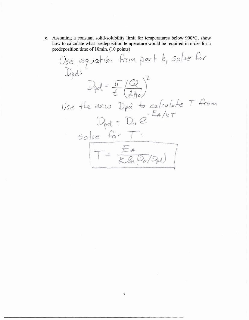
c. Assuming a constant solid-solubility limit for temperatures below 900°C, showhow to calculate what predeposition temperature would be required in order for apredeposition time of 10min. (10 points)
05e e'tUG+I~ +(O>V\. p<u+ bj so(ve .Q,{Dp"!' ~ 2-
])pc{~f&~Jlhe +k MeW Dpot -Iv ca.(c.Ja.le T +'-0-1-1
-E4/k T'Il.,.n - ~oevf~ u
'Solve .Po, T~
\T-- :~l[)o/~j(-- .. " 1
7
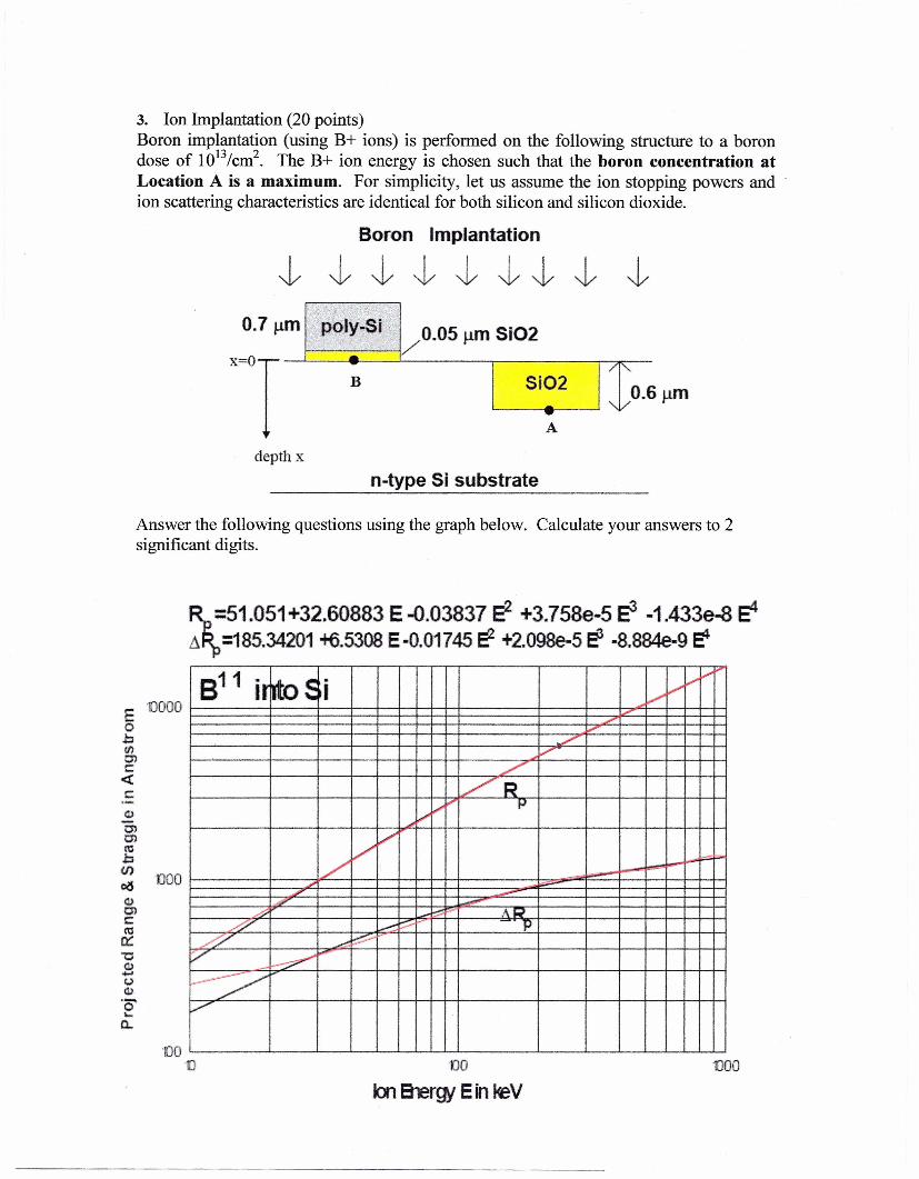
3. Ion Implantation (20 points)Boron implantation (using B+ ions) is performed on the following structure to a borondose of 1Q13/cm2. The B+ ion energy is chosen such that the boron concentration atLocation A is a maximum. For simplicity, let us assume the ion stopping powers and -ion scattering characteristics are identical for both silicon and silicon dioxide.
Boron Implantation
poly-Si /0.05 J.1m Si02-- / I"B Si02
I/0'- -,-
0.7 J.1ffi
A
depth x
n-type Si substrate
Answer the following questions using the graph below. Calculate your answers to 2significant digits.
E DOOO0b(/)0)c:~c:(!.)
0)0)C'ObCJ)
1JOO06(!.)0)cC'O0::"'0
(!.).•...r.>(!.)
'0'•..a..
f\ =51.051 +32.60883 E -0.03837 e2 +3.758e-5 eJ -1.433e-8 e4~~=185.34201-+6.5308E-O.01745 ~ +2.098e-5 El -8.884e-9 t:4
811 ir Jto~. ~ J..'"
I V ~
.....-./'
""/'"
/R.,,""~
/'"/"
/-•....-""""
" ---'H' ...--
A !,:::: po' AkJ~ ~ V- P
~ ~ ~v ~ .--?./""
DO-I) 1')0
b1 ~rgy E in leVeoo
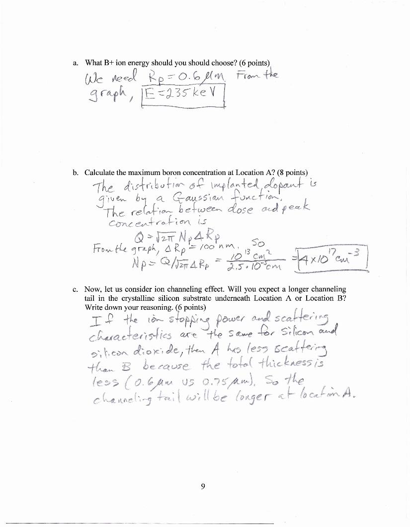
a. What B+ ion energy should you should choose? (6 points)(jJL tAeee2 K ::-O. ~ VV\. tTOW'- tk..5 '''-f''- I lE c:: d-~ If ~
c. Now, let us consider ion channeling effect. Will you expect a longer channelingtail in the crystalline silicon substrate underneath Location A or Location B?Write down your reasoning. (6 points) ( 1_ ~I ~ f4 tb- s+o~~·(~ p~we( ~ sc~.rter'~CkCLC-~e('(5..{ jC5 0\~ =tLe s t£.-e ~r S((~CGv"\ ~
~', \\ coe-. J.~0 )C", Je.I ~ A- ~'5 (eS? 6Ca).-I--e/(~-r~.... be CC(f..)$e ~e +0+0-£ flli"klt€S5 is
(e:>~ ( O. ~~tV "us O.75'~w..), SQ -/l.e '-(
r i· l t, I / I I I AC ..t.l\e\~"j' ct, £'V{ II \Q~ t()t...jer" ~t- {()C~,~ ••
9

4. Metallization (25 points)a. List two benefits of using chemical mechanical polishing for multilevel metal
process integration. (4 points) (\ t> fI, ~e Jv cei Jepfl o-t-- +0 ~v5 re1e.) 'r(e~2- Kdv~ 0vud-J. +i~,J" c, b '5 ~5 {I<o $Ir~~~., . .:r:."",yoVJ-;;+eI' Ct>~e«':je -G..-.{'i I""" k f 0 sA,;"", .
b. Assume copper has an electromigration failure activation energy EA = 0.66 eV.The activation energy for aluminum is EA = 0.5 eV. If the same MTF was desiredbetween Cu and Allines, how much more current density can be passed throughCu lines over Allines at 400K? (4 points)
M'P.J.. JLe 1f [ l='A/kTJCL-t 10DC) k:..T-== () ,0347 e V
_ '2.. 0, c,c,P,f)3tf7
*v e > = I,-2.. e" st» ,0.:3..;.-'t 7..:..--:-r----.-\
~41 ~'C,o3¥7;Je -=e~_--r-.".....IJ..:;- ()•s:/. oJ'f)S,41 e
c. Copper has lower resistivity and less susceptibility to electromigration failure.However, it is also a deep-level impurity that can destroy MOS devices. How dowe prevent Cu contamination once the metal lines are formed? (2 points)
10

d. How does adding a small (1-4%) of Cu impurity improve the electromigrationresistance of AI? (2 points)
11