MicroTCA.3 Test Plan
20
MicroTCA.3 Test Plan Hardened Conduction Cooled MicroTCA System Testing For Validation of MicroTCA Backplane to AMC Connector System Revision 1.2 December 21, 2009 Written By: Approved By: BAE Systems, Mark Leibowitz BAE Systems, Michael Borthwick Hybricon, Michael R. Palis Cisco Systems, Kevin Casey Cypress Point Research, Joe Pavlat Elma Electronics, Eike Waltz Extrusion Technology, Steve Richardson GE Intelligent Platforms, Jeff Marden Harting Inc., Andreas Kohler Hybricon Corp, Bob Sullivan Kontron, David Pursley VadaTech, Saeed Karamooz Wavetherm, Rodney Bame David Mosier
Transcript of MicroTCA.3 Test Plan

MicroTCA.3
Test Plan
Hardened Conduction Cooled MicroTCA System Testing
For Validation of MicroTCA Backplane to AMC Connector System
Revision 1.2 December 21, 2009
Written By: Approved By: BAE Systems, Mark Leibowitz BAE Systems, Michael Borthwick Hybricon, Michael R. Palis Cisco Systems, Kevin Casey
Cypress Point Research, Joe Pavlat Elma Electronics, Eike Waltz Extrusion Technology, Steve Richardson GE Intelligent Platforms, Jeff Marden Harting Inc., Andreas Kohler Hybricon Corp, Bob Sullivan Kontron, David Pursley VadaTech, Saeed Karamooz Wavetherm, Rodney Bame
David Mosier
PICMG Rugged MicroTCA.3 Module Test Plan Revision 1.2
i
Revision History
Revision Changes Date
0.9 Draft copy 09/01/09 1.0 First review 11/30/09 1.1 Second review 12/01/09 1.2 Third review 12/17/09 1.2 Initial Release (updated approved by names) 12/21/09

PICMG Rugged MicroTCA.3 Module Test Plan Revision 1.2
- 1 -
SCOPE Test plan for qualification testing of the MicroTCA Connectors as manufactured and submitted by the test sponsor on representative conduction Cooled MicroTCA test Modules. This is based on MIL-STD-810 and RTCA/DO-160 environmental tests and the test sequences described in the VITA VPX Test Report; which can be downloaded at:
http://www.vita.com/VITA46ContechTestReportrev1.4.pdf Goal The goal of this test plan is to outline the testing sequence for the AMC and backplane connector used in Rugged MicroTCA.3 Systems. The module portion of the test plan is setting the goal of having test data available to show that the edge mounted connector system proposed for adoption for Rugged MicroTCA products meets the environmental requirements proposed for the Rugged and Hardened MicroTCA Product Specifications. APPLICABLE DOCUMENTS Unless otherwise specified, the following documents of issue in effect at the time of testing form a part of this report to the extent as specified herein. The requirements of sub-tier specifications and/or standards apply only when specifically referenced in this test plan. Test Specifications: The following specifications are provided for reference and the basis point for discussion of testing that is to be targeted as a result of this plan.
o MIL-STD-810F, Environmental Engineering Considerations and Laboratory Tests
o EIA-364, Electrical Connector Test Procedures o EN-61000-4-2, Electrostatic Discharge Immunity Test o ASTM G-85, Standard Practice for Modified Salt Spray Testing

PICMG Rugged MicroTCA.3 Module Test Plan Revision 1.2
- 2 -
TEST SAMPLES AND PREPARATION The following test samples for module testing shall be submitted by the test sponsor for the evaluation to be performed by the test laboratory:
Module Testing: (1) Qty. 18 Conduction Cooled MicroTCA Event Detector AMC (EDA) Modules compliant with AMC.0 Revision 2 as well as the following:
PICMG AMC form factor with AMC edge connector capable of contact monitoring in accordance with MicroTCA.1 Section 10.2.3
PICMG AMC form factor with AMC PWB edge fingers (qty 16) and plug connector (qty 2)
See Appendix A to this Test Plan for the definition of the board characteristics required for module testing.
(2) Qty. 8 MicroTCA backplanes with connectors to support single size AMC modules. Note: Test Group 3 (IR/DWV) is to be performed by the connector manufacturers and would require 2 EDA’s and 1 Backplane, included in above quantities.
The following additional materials shall be submitted by the test sponsor to assist and perform the testing of items listed above.
(1) Holding Test Fixture with machined conduction rail slots and backplane retention, see Table 1 for resource allocation for required test fixtures/chassis’
The test samples shall be certified by the manufacturer as being fabricated and assembled utilizing normal production techniques common for this type of product and inspected in accordance with the quality criteria as established for the product involved. Connector test samples are to be supplied assembled and terminated to test boards by the test sponsor for each of the respective test suites. These tests suites are for conduction cooled MicroTCA Modules. All test samples module test pieces shall be coded and identified by the test sponsor to maintain continuity throughout the test sequences. Upon initiating testing, mated test samples shall remain with each other throughout the test sequences for which they were designated and are not to be interchanged with any other mated connections.

PICMG Rugged MicroTCA.3 Module Test Plan Revision 1.2
- 3 -
TEST SELECTION All tests shall be performed in accordance with the applicable sequences and procedures as defined below. TEST SEQUENCES Figure 1 MicroTCA.3 Module Test Flow shows the test sequences for the module assemblies that are to be tested subsequent to the completion of the contact testing. This sequence of testing is for Module Assembly test to show compliance of the module to the environmental requirements stated within this document.

PICMG Rugged MicroTCA.3 Module Test Plan Revision 1.2
4
LLCREvery
168 Hours
LLCR
1Test Group
Mechanical Shock
RandomVibration
( 1 Hour/ Axis)
LLCR
2
Durability(200 cycles)
No offset
LLCR
Thermal Shock
( 5 Cycles)
LLCR
LLCR
Thermal CyclingW/Humidity(500 Hours)
Durability(200 cycles)
No offset
5
LLCR
LLCR
MFG(5 Days)
LLCR
Durability(200 cycles)
No offset
Engage Force
Separating Force
4
LLCR
LLCR
TemperatureLife
(500 Hours)
LLCREvery
168 Hours
LLCR
6
LLCREvery
168 Hours
Thermal Cycling(500 Cycles)
LLCR
8
Dust
LLCR
SaltFog
w/ SO2(2 -24 Hours)
LLCR
7
LLCR
Group 1 Group 2 Group 4 Group 5 Group 6 Group 7 Group 8# of Backplanes 1 1 1 1 1 1 1
# of EDA’s 41 2 2 2 2 2 2Chassis Type BAE WT WT BAE WT BAE2 WT3
Notes:WT:Wavetherm Chassis BAE: BAE Chassis
2. BAE Chassis for Group 7 Testing (Salt Fog) is taken following completion of the Group 1 Testing with a new backplane installed3. Wavetherm Chassis for Group 8 Testing (Dust) is taken following the completion of Group 2 testing with a new backplane installed.
3
DWV
IR
IR
Thermal Shock
(5 Cycles)
DWV
Thermal CyclingW/Humidity(500 Hours)
IR
DWV
Test
Gro
up 3
to b
e do
ne b
y co
nnec
tor m
anuf
actu
rer
LegendLLCR: Low Level Circuit ResistanceIR: Insulation ResistanceDMV: Dielectric Withstanding VoltageMFG: Mixed Flow GasEDA: Event Detector AMC
Test Flow DiagramRevision E 12/14/09
1. 2 EDA’s with PWB edge fingers & 2 EDA’s with plug edge fingers.
Table 1. Resource Allocation
Figure 1. MicroTCA.3 EDA Test Flow
All test groups are tested with a 0 offset of the EDA to backplane connector.

PICMG Rugged MicroTCA.3 Module Test Plan Revision 1.2
5
Connector Vendor Input & Responsibility The connector products shall have supporting test available showing compliance the for Group 3 testing. This can be presented either in the format of internal testing at the manufacturers’ internal testing resources or via an independent test laboratory. See Figure 1, Test Flow for Group 3 testing requirements. Tests Mechanical Shock:
EIA-364-27B-2009 Test Condition A ; 50 G, 11 millisecond, half sine pulse Requirements:
o MS1: No Physical Damage o MS2: No electrical anomalies/event greater than 10 nanoseconds,
8 daisy chained positions per test sample, for event detection
Random Vibration:
EIA-364-28E-2006 Test Condition V, Letter D, 11.95 Grms, 50 to 2000 Hz Duration: 1 hour per axis for all three orthogonal axes. Requirements:
o RV1: No Physical Damage o RV2: No electrical anomalies/event greater than 10 nanoseconds,
8 daisy chained positions per test sample, for event detection o RV3: LLCR : + 10.0 milliohm maximum change
PICMG Rugged MicroTCA.3 Module Test Plan Revision 1.2
6
Thermal Shock:
EIA-364-32E-2008 o Test Condition A: -55 °C to 85°C, dwell at each extreme for 30
minutes, for five cycles, with a change in temperature that shall occur within 5 minutes between extremes
Requirements: o TS1: No Physical Damage o TS2: Group 2 Samples: LLCR : + 10.0 milliohm maximum change o TS3: Group 3 Samples:
a) IR: 500 Mega ohm Minimum b) DWV: 600 VAC
Thermal Cycle with Humidity
EIA-364-31C-2008 Test Condition III:
o 25°C to 65 °C at 90 % to 95 % Relative Humidity (RH) o Eight Hours Cycles o 63 Cycles (500 Hours)
Requirements: o TCwH1: No Physical Damage o TCwH2: Group 2 Samples: LLCR : + 10.0 milliohm maximum
change on a weekly basis o TCwH3: Group 3 Samples:
a) IR: 500 Mega ohm Minimum b) DWV: 600 VAC
Temperature Life
EIA-364-17B-1999 Test Condition A : 85 °C, Duration: 500 hours Requirements:
o TL1: No Physical Damage o TL2: Group 4 Samples: LLCR: + 10.0 milliohm maximum change,
measured on a weekly basis.

PICMG Rugged MicroTCA.3 Module Test Plan Revision 1.2
7
Mixed Flowing Gas (MFG) EIA-364-65A-1998 Test Condition IIA:
o Chlorine: 10 ppb o Hydrogen Sulfide: 10 ppb o Nitrogen Dioxide 200 ppb o Sulfur Dioxide: 300 ppb o Temperature: 30 °C o Relative Humidity: 70 % RH
Mating Conditions: o Day 1 to Day 5: Samples Unmated o Day 6 to Day 10: Samples Mated
Duration: 10 Days Total Requirements:
o MFG1: No Physical Damage o MFG2: LLCR at both 5 and 10 days: + 10.0 milliohm maximum
change Insulation Resistance (IR)
EIA/ECA-364-21D-2008 Test all adjacent Contacts Level 500 Vdc Requirements:
o IR1: 5000 Mega ohms Minimum Dielectric Withstanding Voltage
EIA-364-20D-2008 Test all adjacent Contacts Requirements:
o DWV1: No Breakdown or flashover arcing at 600VAC Durability
EIA-364-09C-2006 Number of Cycles: 200 min, with a design goal of 500 Cycles. Rate: Ten Cycles per Minute Requirements:
o D1: No Physical Damage o D2: LLCR: + 10.0 milliohm maximum change
Engaging Force/Separating Force
EIA-364-13 Measure the force to engage and separate the Event Detector AMC or
connector samples Requirements:
o EF1: Engaging Force: 100 N Maximum o SF1: Separating Force: 65 N Maximum
PICMG Rugged MicroTCA.3 Module Test Plan Revision 1.2
8
Thermal Cycle
EIA/ECA-364-100-2006 Test Condition C
o 0°C to 110 °C o 10 minute dwell at temperature extremes o Ramp Rate between extremes: 5 °C to 10 °C per minute
Duration 500 cycles Requirements:
o TC1: No Physical Damage o TC2: LLCR: + 10.0 milliohm maximum change
Salt Fog
ASTM G85, Annex A4 (cycle A4.4.4.1), two 24 hr. cycles Requirements:
o SF1: LLCR: + 10.0 milliohm maximum change o SF2: No excessive corrosion product build up between backplane
connector and EDA PWB edge finger contacts Dust
MIL-STD-810, Method 510.4, Procedure II Requirements:
o D1: LLCR: + 10.0 milliohm maximum change T Test Verification Methods Low Level Circuit Resistance (LLCR)
EIA-364-23C-2006, TP-23C 100 milliamp max., 20 millivolts, 52 resistance positions Data: Record Measured Level
Nanosecond Event Detection
EIA-364-87A, TP-87A No events greater then 10ns, 8 daisy chained positions Data: Record Measured Level
PICMG Rugged MicroTCA.3 Module Test Plan Revision 1.2
A1
Appendix A: EDA & Backplane Requirements: EDA to backplane alignment requirement: All EDA boards (Unit Under Test [UUT]) to backplane connection interfaces shall be in accordance with the requirements in this test plan. The following figures and tables are provided to specify specific requirements for testing for the module taking into account system design issues and known good design practices for plating systems in dynamic environments. Figure 1: EDA PCB To backplane connector Centerline normalized.
Requirement A1: All test groups shall be conducted with 0 offset between the EDA and backplane connector centerline to support the normalized system installation of the EDA, see figure 1 above. Requirement A2: To align the backplane to the EDA, loosely screw in the backplane and insert EDAs into slots 2, 4, 6, and 8. Tighten all EDA wedgelocks (quantity 8) and then tighten all of the screws holding the backplane to the chassis to 5 +/-0.5 in-lbs.
2
Backplane
M
Side 1
Contact
Fully inserted connector must Bottom.Wedge Lock expanded
1.6+/-0.16ReferencePCB
ModuleClam Shel ls
Cold Wall
Cold W all toModuleThermal interphase
Wed
ge lo
ck
3
Module/Cold W all thermal interface
Subrack Cold Wall
W edge Lockexpanded
backp lane
ModuleClam Shell
Connector
M
Side 1 of PCB and Module Cold Wall inter face
0.8 +/-0.08

PICMG Rugged MicroTCA.3 Module Test Plan Revision 1.2
A2
Figure 2: Event Detector AMC Electrical requirements
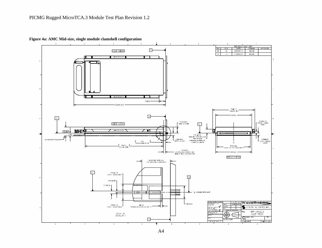
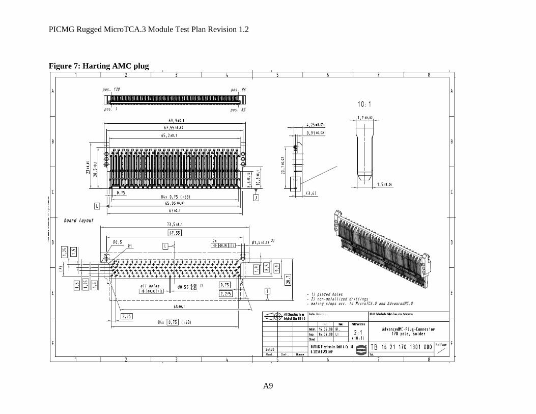
Requirement A3: EDA wiring and pin assignments for determination of loss of contact and resistance during the testing shall be in accordance with the requirements of Figure 2 above, which is a requirements extraction of MicroTCA.1, Section 10.2.2. Requirement A4: 52 contact resistance points shall be bussed together on the EDA and 2 electrical traces shall be brought to the front panel side of the EDA and terminated to a 0.040 plated thru hole for voltage and current measurements during LLCR testing, see figure 8, LLCR set up. Requirement A5: The recommended clamshell arrangement for all module testing is recommended to be the mid-size, single module that is shown in Figures 4a & 4b. Requirement A6: The EDA shall support both AMC PWB edge finger design and the Harting MicroTCA plug, see figure 7 per PICMG AMC.0 Rev. 2.0.

PICMG Rugged MicroTCA.3 Module Test Plan Revision 1.2
A3
Requirement A7: The EDA shall have a maximum weight for a mid-size, single width AMC Module including lower & upper clam shell sections and wedgelocks, test weights screwed to PWB, and PWB of 650g (-5%, +0%). The weight shall be distributed in accordance with figure 3 below. Figure 3: EDA mass loading (clam shell not shown)
PCB Mater ial FR4Other Dims as per AMC Spec
CL
(1.60)
M3 boltsx 8
12.0 max
38.045.070.076.0102.0108.0133.0140.0
16.0
38.5
61.0
PICMG Rugged MicroTCA.3 Module Test Plan Revision 1.2
A4
Figure 4a: AMC Mid-size, single module clamshell configuration

PICMG Rugged MicroTCA.3 Module Test Plan Revision 1.2
A5
Figure 4b: AMC Mid-size, single module clamshell configuration

PICMG Rugged MicroTCA.3 Module Test Plan Revision 1.2
A6
Table 1: Printed Wiring Contact & Connector Plating Requirements Plating Parameter Specific Requirement: Minimum Gold Plating Thickness 30 micro-inches Gold Plating Thickness Preference 50 micro-inches Gold Sub Plating 75 micro-inches, min. Nickel over Copper Gold Plating Hardness Hard Gold Requirement A8: Contact and edge finger test item plating required to meet the minimum requirements for plating and plating system as shown in Table 1. Backplane requirements The VadaTech VT870 backplane, see figure 5 below will be modified to be used for the tests defined in this test plan. The backplane will be used with the BAE Systems MicroTCA ATR chassis and the Wavetherm MicroTCA test chassis. Only slots 2, 4, 6, 8 and 10 will be populated with the Harting MicroTCA connector, remaining connectors will not be populated. Slot 1, Power Module connector can be populated for future testing requirements. Figure 5: VT870 MicroTCA backplane
Backplane Electrical requirements: Requirement: All mid-size slots shall have the following:
• A9: All contact resistance contacts, defined in figure 2 shall be measured for voltage and current during LLCR on the back side of the backplane at the connector termination point, see figure 7.
• A10: Each discontinuity loop back contact pairs, defined in figure 2 shall be terminated to a Plated Thru Hole (PTH), 0.40 inches with a pair spacing of 0.10 inches on the back side of the backplane to solder RG174U coax cable for use with the event detector.
PICMG Rugged MicroTCA.3 Module Test Plan Revision 1.2
A7
Backplane Mechanical requirements: Requirement: Mechanical layout of the backplane shall not change except for the following:
• A11: MicroTCA connectors shall be changed to support the Harting MicroTCA 50 micro-inch gold over Ni connector defined in figure 6.
• A12: Electrical test points for the contact resistance contacts for all mid-sized slots added as defined above to facilitate LLCR testing.
• A13: Electrical test points for the discontinuity loop back contact pairs for all mid-sized slots added as defined above to facilitate event detection testing.
Data Reporting Recommendations: Visual documentation and measured data should be presented in a formal report documenting the test performed and the conditions that these test were performed under. Significant results should be presented at measurements or presentation of significant results, both positive and negative results. Photographs, plating micrographs and test plots are all examples of test result data presentation and do not need to be limited to this list. The goal of this data presentation is to provide objective test evidence that the test items are meeting the aggressive environmental tests that are being specified for Conduction Cooled MicroTCA.3 modules.

PICMG Rugged MicroTCA.3 Module Test Plan Revision 1.2
A8
Figure 6: Harting 50 miro-inch of Au over Ni MicroTCA connector
PICMG Rugged MicroTCA.3 Module Test Plan Revision 1.2
A9
Figure 7: Harting AMC plug

PICMG Rugged MicroTCA.3 Module Test Plan Revision 1.2
A10
Figure 8: LLCR Set Up Note Above setup does not show all contacts under test.
This is a trace that connects all the LLCR positionTogether creating a “common buss”.
LLCR SET UP +V +I
BackplanePCB
Contactunder test
‐I‐V
Contact undertest
2 separate traces are terminated to each pos ition under test for LLCR. A PTH is added to the end of the trace.