Microprocessors and microcontrollers PIC and ARM - Home -...
78
Microprocessors and microcontrollers PIC and ARM
Transcript of Microprocessors and microcontrollers PIC and ARM - Home -...

Microprocessors and microcontrollers
PIC and ARM
3213: Digital Systems & Microprocessors: L#20(Source: Dr Sandra I. Woolley. Uni Birmingham, UK)
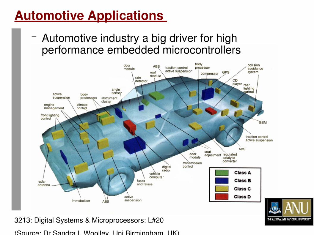
Automotive Applications – Automotive industry a big driver for high
performance embedded microcontrollers


3213: Digital Systems & Microprocessors: L#2223
PIC16F84 (old but venerable)

3213: Digital Systems & Microprocessors: L#20
Misc PIC16F84 Functions
● OSC Selection
● RESETs Poweron Reset (POR), Powerup Timer (PWRT), Oscillator Startup Timer (OST)
● Interrupts
● Watchdog Timer (WDT)
● SLEEP
● Code Protection
● ID Locations

3213: Digital Systems & Microprocessors: L#19
PIC16F84 PINS
3213: Digital Systems & Microprocessors: L#19
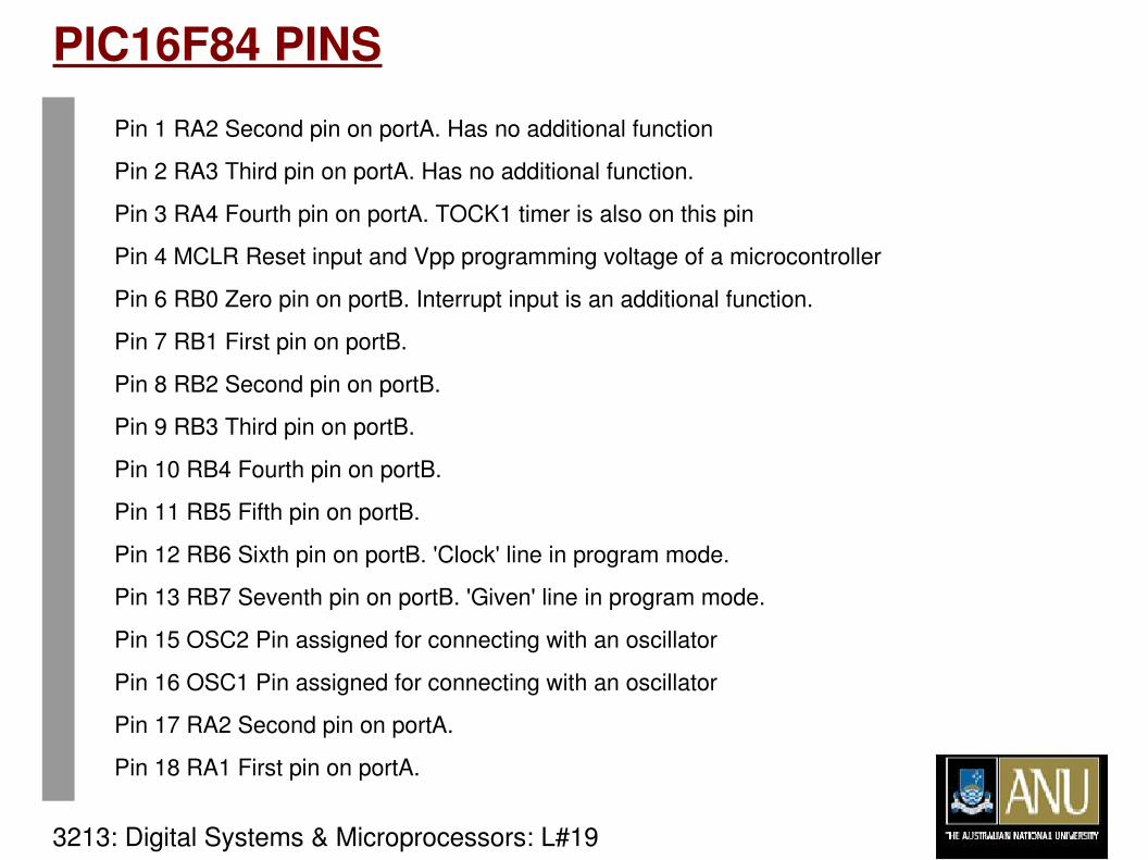
PIC16F84 PINSPin 1 RA2 Second pin on portA. Has no additional functionPin 2 RA3 Third pin on portA. Has no additional function.Pin 3 RA4 Fourth pin on portA. TOCK1 timer is also on this pinPin 4 MCLR Reset input and Vpp programming voltage of a microcontrollerPin 6 RB0 Zero pin on portB. Interrupt input is an additional function.Pin 7 RB1 First pin on portB. Pin 8 RB2 Second pin on portB. Pin 9 RB3 Third pin on portB. Pin 10 RB4 Fourth pin on portB. Pin 11 RB5 Fifth pin on portB.Pin 12 RB6 Sixth pin on portB. 'Clock' line in program mode.Pin 13 RB7 Seventh pin on portB. 'Given' line in program mode.Pin 15 OSC2 Pin assigned for connecting with an oscillatorPin 16 OSC1 Pin assigned for connecting with an oscillatorPin 17 RA2 Second pin on portA. Pin 18 RA1 First pin on portA.

Hig Performance RISC CPU
• Only 35 single word instructions to learn • All instructions singlecycle except for program branches which are twocycle • Operating speed: DC 20 MHz clock input DC 200 ns instruction cycle • 1024 words of program memory • 68 bytes of Data RAM • 64 bytes of Data EEPROM • 14bit wide instruction words • 8bit wide data bytes • 15 Special Function Hardware registers • Eightlevel deep hardware stack • Direct, indirect and relative addressing modes • Four interrupt sources: External RB0/INT pin TMR0 timer overflow PORTB<7:4> interruptonchange Data EEPROM write complete
3213: Digital Systems & Microprocessors: L#20

3213: Digital Systems & Microprocessors: L#20
PIC16F84 Instruction set
●For byteoriented instructions, 'f' represents a file register designator and 'd' represents a destination designator. The file register designator specifies which file register is to be used by the instruction.●The destination designator specifies where the result of the operation is to be placed. If 'd' is zero, the result is placed in the W register. If 'd' is one, the result is placed in the file register specified in the instruction.●For bitoriented instructions, 'b' represents a bit field designator which selects the number of the bit affected by the operation, while 'f' represents the address of the file in which the bit is located.●For literal and control operations, 'k' represents an eight or eleven bit constant or literal value.

3213: Digital Systems & Microprocessors: L#20
Opcodes

Instruction set
3213: Digital Systems & Microprocessors: L#20

Instruction set
3213: Digital Systems & Microprocessors: L#20


3213: Digital Systems & Microprocessors: L#20(Source: Dr Sandra I. Woolley. Uni Birmingham, UK)
Simple Assembly LanguageLet us look at some examples of PIC16F84 microcontroller assembler instructions. What do these instructions do?
At the start, the working register (W) contains the value 0x1C and the PORTB register contains the value 0. What values are in W and PORTB after each instruction?
MOVLW 0X24 ADDLW 0X02 ADDLW 0X17 MOVWF PORTB CLRWADDLW 0x05MOVWF PORTBCLRF PORTB

; WRITTEN BY SIW; DATE 01/01/2004; FILE SAVED AS TEST.ASM; DEVICE 16F84; OSCILLATOR XT (4MHZ); WATCHDOG DISABLED; FUNCTION OUTPUTS THE VALUE 0XF1 TO 8 LEDS CONNECTED TO PORTB; EQUATES PORTB EQU 0X06 ;ASSIGN THE PORTB REGISTER TO THE LABEL 'PORTB'; MAIN PROGRAM START ORG 0X00 ;'ORG' SPECIFIES THE MEMORY LOCATION OF THE PROGRAM MOVLW 0X00 ;MOVE THE VALUE 00, I.E., ALL 0'S TO W TRIS PORTB ;CONFIGURE PORTB WITH THE VALUE IN W (THE ;WORKING REGISTER) 1=INPUT AND 0=OUTPUT. ;SO 00 (ALL 0'S) MAKES ALL PORTB LINES OUTPUTS. CLRF PORTB ;CLEAR THE PORTB REGISTER MOVLW 0XF1 ;MOVE THE HEX VALUE F1 TO THE WORKING REGISTER MOVWF PORTB ;OUTPUT THE VALUE TO PORTBLOOP GOTO LOOP END
3213: Digital Systems & Microprocessors: L#20(Source: Dr Sandra I. Woolley. Uni Birmingham, UK)
Simple Assembly Language

3213: Digital Systems & Microprocessors: L#21
How to Assemble PIC Assembly Language
WINDOWS: MPLAB from MicroChip (free download from http://www.microchip.com)
LINUX: use GPASM part of GPUTILS package
Neither provide a C compiler

3213: Digital Systems & Microprocessors: L#21
Example: Write to PORTB;--Program "Port.asm". A simple program to write a byte to PORTB.
;--Author: Montague Paravrov-Nikots.
;--Date: 7 July 1997.
;--Version: 1.01
LIST p=PIC16C84, r=hex, f=INHX8M
include "P16C84.inc"
org 0x0 ; Reset vector.
;--Set up the pins of PORTB to act as outputs.
;--Select Bank 1 to access TRISB register.
bsf STATUS,RP0 ; Select Bank 1.
clrf TRISB ; Make all PORTB pins outputs.
;--Switch back to Bank 0 to access PORTB register.
bcf STATUS,RP0 ; Back to Bank 0.
;--Load a byte into PORTB.
movlw B'10110101' ; Move a byte into the working register.
movwf PORTB ; Move contents of W into PORTB register.
wait goto wait ; Loop forever until power is removed.
end ; End of program "Port.asm".

3213: Digital Systems & Microprocessors: L#21
P16C84.inc: Header file
; This header file defines configurations, registers, and other
useful bits of
; information for the PIC16C84 microcontroller. These names are
taken to match \
; the data sheets as closely as possible.
; Note that the processor must be selected before this file is
; included. The processor may be selected the following ways:
; 1. Command line switch:
; C:\ MPASM MYFILE.ASM /PIC16C84
; 2. LIST directive in the source file
; LIST P=PIC16C84
; 3. Processor Type entry in the MPASM full-screen interface

List of MACROS
;----- Register Files-----------------------------------
INDF EQU H'0000'
TMR0 EQU H'0001'
PCL EQU H'0002'
STATUS EQU H'0003'
FSR EQU H'0004'
PORTA EQU H'0005'
PORTB EQU H'0006'
EEDATA EQU H'0008'
EEADR EQU H'0009'
PCLATH EQU H'000A'
INTCON EQU H'000B'
OPTION_REG EQU H'0081'
TRISA EQU H'0085'
TRISB EQU H'0086'
EECON1 EQU H'0088'
EECON2 EQU H'0089'
3213: Digital Systems & Microprocessors: L#21
P16C84.inc: Sample Lines

gpasm project1asm.asm > the HEX file
:0C000000831686018312B53086000528A7
:00000001FF
:0C000000 (83 1) (6 86) (01 83 1)
(2 B5) 30 86 000(5 28)(A7)
:00000001FF
bsf STATUS,RP0
clrf TRISB
bcf STATUS,RP0
movlw B'10110101'
movwf PORTB
wait goto wait
end
3213: Digital Systems & Microprocessors: L#21
GPASM (the assembly language compiler)
Checksum
B'10110101'
TRISB
STATUS
No need to encode 'wait'

3213: Digital Systems & Microprocessors: L#21
The C Programming Language
C is a high level language... Looks more like VERILOG than assembly language. Dennis Ritchie (Circa 1973)
LINUX and WINDOWS are written in C
Can use C to program PICs and to written complex software involving Graphical User Interfaces (GUIs)
C++ = Object oriented C.

3213: Digital Systems & Microprocessors: L#21
The C Versions
C has an ANSI standard form “ANSI Standard C”.
Particular versions of C for different applications: Microsoft C, GNU C for Intel, uCLINUX and SDCC for embedded devices.
Can use C to program PICs as well as to write complex software involving Graphical User Interfaces (GUIs)... just depends on the compiler.

main module
preprocessor directive
printf.. the most usefuldebugging tool
3213: Digital Systems & Microprocessors: L#22
main module and printf()

3213: Digital Systems & Microprocessors: L#22
subroutine of type int
for loop
literal
TheByte is returned. But mostly you return the status of the call
C modules, type, control loops, return values

3213: Digital Systems & Microprocessors: L#22
More data types
floating point and double precisionshort 16 bitint, long 32 bit
char = 8 bit (the byte!)
strings are pointersto chars

3213: Digital Systems & Microprocessors: L#22
Maths in C
Math header
Preprocessor directive #define
cosine, sine, log, exp etc

3213: Digital Systems & Microprocessors: L#22
Read files
headersCommand line arguments
Reading here

3213: Digital Systems & Microprocessors: L#22
Pointers
q and j passed by referencek passed only by value
Pointers point to memoryoccupied by a variable.
Use the * operator
A pointer
Assigning a value to a pointer
Question:
What happens to p, i and k?
The & gives the adddress of the variable following it

3213: Digital Systems & Microprocessors: L#22
What output does this code produce?

More fun with pointers: KEEP IT SIMPLE STUPID PROTOCOL
3213: Digital Systems & Microprocessors: L#22
*ptr++ look at memory addressof ptr and increment by 1
C even has case

3213: Digital Systems & Microprocessors: L#21
Small Device C Compile (SDCC)
What is SDCC?
SDCC is a retargettable, optimizing ANSI C compiler that targets the Intel 8051, Maxim 80DS390, Zilog Z80 and the Motorola 68HC08 based MCUs.
Work is in progress on supporting the Microchip PIC16 and PIC18 series.
SDCC is Free Open Source Software, distributed under GNU General Public License (GPL)

3213: Digital Systems & Microprocessors: L#21
The Compiling process with SDCC

3213: Digital Systems & Microprocessors: L#21
Doing it in C.../*
project1.c
GGB
sdcc -mpic14 -p16f84 project1c.c
*/
/* Define processor and include header file. */
#define __16f84
#include"pic/pic16f84.h"
// Set the __CONFIG word:
typedef unsigned int word;
word at 0x2007 __CONFIG = 0x3f72;
void main(void) {
unsigned char PB = 0xD5;
/* PORTB.1 is an output pin */
TRISB = 0;
PORTB = PB;
while(1) { /* Loop forever */ }
}
Preprocessor directives
always a main methodan unsigned byte specified in HEXformat
PORTB and TRISRB are variables .. not memory addresses

[ggb112@localhost C]$ sdcc -mpic14 -p16f84 project1c.c
message: using default linker script
"/usr/local/share/gputils/lkr/ "
[ggb112@localhost C]$ ls -l
total 36
-rw-rw-r-- 1 ggb112 ggb112 3326 May 24 16:32 project1c.asm
-rw-rw-r-- 1 ggb112 ggb112 389 May 24 16:19 project1c.c
-rw-rw-r-- 1 ggb112 ggb112 5120 May 24 16:32 project1c.cod
-rw-rw-r-- 1 ggb112 ggb112 1264 May 24 16:32 project1c.hex
-rw-rw-r-- 1 ggb112 ggb112 9661 May 24 16:32 project1c.lst
-rw-rw-r-- 1 ggb112 ggb112 1772 May 24 16:32 project1c.o
[ggb112@localhost C]$
sdcc S mpic14 p16f84 project1c.c... just compiles only (produces the ... .asm file)3213: Digital Systems & Microprocessors: L#21
The Compiling process with SDCC

project1c.asm contains the output of compiler and contains the assembly
language version of the C code.
project1c.o contains the output of gpasm.
project1c..lst contains debugging information form the linker.
project1c.hex contains the final PIC program in a format suitable to
download into your programmer.
project1c.cod contains a version of the final program with additional
information that can be used with gpsim.
Now you need to use your programmer to transfer project1c.hex into your
PIC
3213: Digital Systems & Microprocessors: L#21
The Compiling process with SDCC

3213: Digital Systems & Microprocessors: L#19
PIC16F84 CPU
GPR and SFR here

3213: Digital Systems & Microprocessors: L#19
CPU and ALU
CPU's most important role is to decode machine language instructions (opcodes) Must be connected to all parts of the microcontroller Data (8 bit) and address (14 bit) busses PIC16F84 has 8 bit ALU and 8 bit WR. With two operands: one in WR and the other either
GPR or SFR. With one operand: either in WR or GPR or SFR.● ALU affects values of Carry (C), Digit Carry
(DC), and Zero (Z) bits in STATUS register.

3213: Digital Systems & Microprocessors: L#19
Memory Organisation ● PIC16F84 has two separate memory blocks, one for data and the other for program. ● EEPROM memory and GPR registers in RAM memory make up the data block.● FLASH memory makes up the program block.
➔ The size of program memory is 1024 locations with 14 bits➔ Locations zero and four are reserved for reset and interrupt vector.
● Data memory consists of EEPROM and RAM memories.➔ EEPROM has 64X8 bit locations of nonvolatile memory.➔ EEPROM memory indirectly accessed thru EEADR and EEDATA registers➔ RAM data memory resides on memory map from 0x0C to 0x4F (68 locations)
● Besides linear division in SFR and GPR, memory is also divided into two banks: BANK0 and BANK1.

PIC16F84 Data Memory Organisation Data memory = GP registers and SFregisters in RAM
and EEPROM data memory Has 8 bit data bus Both GPR and SFR are banked SFR are first 12 registers of each bank. GPR banked to give 116 bytes of static RAM data
storage Banking requires control bits (status register) for bank
selection Bank0 is selected by clearing RP0 (Status<5>) or
Bank1 by setting that bit. The entire memory can be accessed either by using the
absolute memory address or Indirectly through the File Select Register (FSR)

PIC16F84 Program Memory Organisation Two separate memory blocks one for data and one for
programs Has 13 bit PC to address 14 bit memory space The first 1k X 14 bit flash program memory (000h –
03FFh) are implemented An access to program space above the max causes
wraparound. The RESET vector is at 0000h and the interrupt vector
is at 0004h.
3213: Digital Systems & Microprocessors: L#20

PIC16F84
Data
Memory
3213: Digital Systems & Microprocessors: L#20

3213: Digital Systems & Microprocessors: L#19
Memory

SFR

3213: Digital Systems & Microprocessors: L#19
Status Register
● STATUS register contains arithmetic status ALU (C (carrier), DC (digit carry), Z (zero test)), RESET status (TO (time-out), PD (power down)) and bits for selecting of memory bank (BANK0 or BANK1) (IRP, RP0 (register bank select bits)). N.B. RP1 not used.
● Because selection of memory bank is controlled through this register, it has to be present in each bank.

3213: Digital Systems & Microprocessors: L#19
Status register
Bit 0: Carry C bit is affected by ADDWF, ADDLW, SUBLW, SUBWF instructions. Set with a bit carry
Bit 1: Digit carry (DC) is affected by ADDWF, ADDLW, SUBLW, SUBWF instructions. Set with a bit carry from fourth bit.
Bit 2: Indication of a zero result. Set when result produces a zero Bit 3: Power down bit. 1 = power up, 0 = sleep mode etc (see datasheet) Bit 4: Timeout. Set while running. Reset by watchdog timer in case of fault. Bit 6:5 RP1:RP0 Register back select bits. Direct addressing Bit 7 IRP Register bank select for indirect addressing

3213: Digital Systems & Microprocessors: L#19
Program Counter and Stack● Program counter (PC) is a 13 bit register that contains the address of the instruction being executed. ● PIC16F84 has a 13 bit, 8 level stack.● Main use of stack is to store the value of the program counter when a branch has occurred.● When moving from a program to a subprogram, the current PC value is pushed onto the stack● The stack value is popped when a return is executed.

3213: Digital Systems & Microprocessors: L#20
The PIC16F84A has 4 sources of interrupt:
∙ External interrupt RB0/INT pin∙ TMR0 overflow interrupt∙ PORTB change interrupts (pins RB7:RB4)∙ Data EEPROM write complete interrupt
The interrupt control register (INTCON) records individual interrupt requests in flag bits. It also contains the individual and global interrupt enable bits. Interrupts recorded on the stack like subroutine branches
Interrupts


3213: Digital Systems & Microprocessors: L#19
Ports● Physical connection to outside world
● A port is a register inside the microcontroller
● Some pins have two functions, some pins have twofold roles like PA4/TOCKI
● Selection done in one of the configurational registers
● An illustration of this is the fifth bit T0CS in OPTION register

3213: Digital Systems & Microprocessors: L#19
Ports: PORTA and PORTB● All pins can be input or output● Need to write a combination of 0's (output) and 1's (input) to
TRISA/TRISB registers● Every port has its proper TRIS register. Thus, port A has TRISA at address 85h, and port B has TRISB at address 86h.

3213: Digital Systems & Microprocessors: L#19
Free Timer TRM0● Counts 0:255 repeatedly
● prescaler divides the timer clock as shown
● Can generate interrupts to program execution

3213: Digital Systems & Microprocessors: L#19
Free Timer TRM0● Programmer must reset TOIF so that a new interrupt can be detected.
● Interrupts can also be generated by an external clock on RA4/TOCK1
● Choosing one of TRM0 and RA4/TOCK1 is chosen by the TOCS in the OPTION register.
●If the external clock is chosen then you can define the edge on which the interrupt is generated.

3213: Digital Systems & Microprocessors: L#19
Clock and Instruction Cycle● Clock from the oscillator enters microcontroller via OSC1 pin where internal circuit of a microcontroller divides the clock into four even clocks Q1, Q2, Q3, and Q4 which do not overlap.●These four clocks make up one instruction cycle (also called machine cycle) during which one instruction is executed.

● Instruction cycle consists of cycles Q1, Q2, Q3 and Q4. ● Cycle of calling begins with Q1 clock, by writing into instruction
register (IR). Decoding and executing begins with Q2, Q3 and Q4 clocks. ● To call and execute an instruction, one instruction cycle is needed, and one
more is needed for decoding and execution. ● With pipelining each instruction is effectively executed in one cycle.
3213: Digital Systems & Microprocessors: L#19
Pipelining normal case without branch instruction

3213: Digital Systems & Microprocessors: L#19
Pipelining normal case without branch instruction●TCY0 reads in instruction MOVLW 55h.●TCY1 executes instruction MOVLW 55h and reads in MOVWF PORTB.●TCY2 executes MOVWF PORTB and reads in CALL SUB_1.●TCY3 executes a call of a subprogram CALL SUB_1, and reads in instruction BSF PORTA, BIT3.
●As this instruction is not the one we need, or is not the first instruction of a subprogram SUB_1 whose execution is next in order, instruction must be flushed and read in again. ●This is a example of an instruction needing more than one cycle.
●TCY4 instruction cycle is totally used up for reading in the first instruction from a subprogram at address SUB_1.●TCY5 executes the first instruction from a subprogram SUB_1 and reads in the next one.

3213: Digital Systems & Microprocessors: L#19
Pipelining with branch
If instruction causes a change in PC, and PC doesn't point to the following but to some other address (which can be the case with jumps or with calling subprograms), two cycles are needed for executing an instruction.

3213: Digital Systems & Microprocessors: L#20
Misc PIC16F84 Functions● OSC Selection
● RESETs Poweron Reset (POR), Powerup Timer (PWRT), Oscillator Startup Timer (OST)
● Interrupts
● Watchdog Timer (WDT)
● SLEEP
● Code Protection
● ID Locations

3213: Digital Systems & Microprocessors: L#19
In System Programming
● In order to program the program memory, the microcontroller must be set to special working regime by bringing up MCLR pin to 13.5V, and supply voltage Vdd has to be stabilized between 4.5V to 5.5V.
● Program memory can be programmed serially using two 'data/clock' pins which must previously be separated from device lines, so that errors do not arise during programming.
● In circuit serial programming (ICSP) is used to program PICs
● There is free software to do this (MPLAB, ICPROG.EXE)

3213: Digital Systems & Microprocessors: L#19
ICSP


3213: Digital Systems & Microprocessors: L#18
Linux usage on Intel (4 level Von Neuman)

Advanced RISC Machines(1990)(ACORN and Apple Computer)
3213: Digital Systems & Microprocessors: L#22_23
ARM Architecture

ARM history• 1983 developed by Acorn computers
– To replace 6502 in BBC computers – 4man VLSI design team– Its simplicity comes from the inexperience team– Match the needs for generalized SoC for
reasonable power, performance and die size• 1990 ARM (Advanced RISC Machine), owned
by Acorn, Apple and LSI
3213: Digital Systems & Microprocessors: L#22_23

ARM LtdDesign and license ARM core design but not fabricate

Why ARM?• One of the most licensed and thus widespread
processor cores in the world– Used in PDA, cell phones, multimedia players,
handheld game console, digital TV and cameras– ARM7: GBA, iPod– ARM9: NDS, PSP, Sony Ericsson, BenQ– ARM11: Apple iPhone, Nokia N93, N800– 75% of 32bit embedded processors
• Used especially in portable devices due to its low power consumption and reasonable performance
3213: Digital Systems & Microprocessors: L#22_23

ARM powered products

Naming ARM• ARMxyzTDMIEJFS
– x: series– y: MMU– z: cache– T: Thumb– D: debugger– M: Multiplier– I: Interrupt– E: Enhanced – J: Jazelle– F: Floatingpoint– S: Source
3213: Digital Systems & Microprocessors: L#22_23

Popular ARM architecture• ARM7TDMI
– 3 pipeline stages– One of the most used ARMversion (for lowend
systems)• ARM9TDMI
– Compatible with ARM7– 5 pipeline stages– Separate instruction and data cache
• ARM113213: Digital Systems & Microprocessors: L#22_23

ARM architecture
• Load/store architecture• A large array of
uniform registers• Fixedlength 32bit
instructions• 3address instructions
3213: Digital Systems & Microprocessors: L#22_23

Processor modes
3213: Digital Systems & Microprocessors: L#22_23

ARM architecture
• 37 registers– 1 Program counter– 1 current program
status registers– 5 saved program
status registers– 30 general purpose
registers
3213: Digital Systems & Microprocessors: L#22_23

Registers• Only 16 registers are visible to a specific mode.
A mode could access– A particular set of r0r12– r13 (sp, stack pointer)– r14 (lr, link register)– r15 (pc, program counter)– Current program status register (cpsr)
3213: Digital Systems & Microprocessors: L#22_23

Register organization
3213: Digital Systems & Microprocessors: L#22_23

Generalpurpose registers08 716 1524 2331
8-bit Byte
16-bit Half word
32-bit word
• 6 data types (signed/unsigned)• All ARM operations are 32bit. Shorter data
types are only supported by data transfer operations.3213: Digital Systems & Microprocessors: L#22_23

Program counter• Store the address of the instruction to be
executed• All instructions are 32bit wide and word
aligned• Thus, the last two bits of pc are undefined.
3213: Digital Systems & Microprocessors: L#22_23

mode bits
Program status register (CPSR)
overflow
carry/borrow
zero
negative
state bit
FIQ disable
IRQ disable
3213: Digital Systems & Microprocessors: L#22_23

28/05/09 Embedded Processor 77
Summary Load/store architecture Most instructions are RISCy, operate in
single cycle. Some multiregister operations take longer.
All instructions can be executed conditionally.
3213: Digital Systems & Microprocessors: L#22_23

28/05/09 Embedded Processor 78