Microprocessor and Microcontroller Unit –I – 8085 Architecture.
33
Microprocessor and Microcontroller Unit –I – 8085 Architecture
-
Upload
jalen-boucher -
Category
Documents
-
view
240 -
download
2
Transcript of Microprocessor and Microcontroller Unit –I – 8085 Architecture.

Microprocessor and Microcontroller
Unit –I – 8085 Architecture

2
8085 Pinout

3
8085 Signals

4
8085 Microprocessor: Functional Block Diagram

Microprocessor Architecture
• The microprocessor can be programmed to perform functions on given data by writing specific instructions into its memory.– The microprocessor reads one instruction at a
time, matches it with its instruction set, and performs the data manipulation specified.
– The result is either stored back into memory or displayed on an output device.

Internal Data Operations• The 8085 can perform a number of internal
operations. Such as: storing data, Arithmetic & Logic operations, Testing for condition, etc.
– To perform these operations, the microprocessor needs an internal architecture similar to the following:
Accumulator FlagsB C
D E
H L
Program Counter
Stack Pointer
DataAddress 816

The ALU
• In addition to the arithmetic & logic circuits, the ALU includes the accumulator, which is part of every arithmetic & logic operation.
• Also, the ALU includes a temporary register used for holding data temporarily during the execution of the operation. This temporary register is not accessible by the programmer.

The Internal Architecture
• We have already discussed the general purpose registers, the Accumulator, and the flags.
• The Program Counter (PC)– This is a register that is used to control the
sequencing of the execution of instructions.– This register always holds the address of the next
instruction.– Since it holds an address, it must be 16 bits wide.
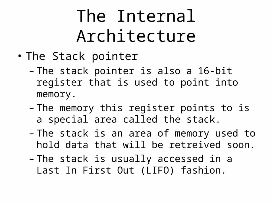
The Internal Architecture
• The Stack pointer– The stack pointer is also a 16-bit register that
is used to point into memory. – The memory this register points to is a special
area called the stack.– The stack is an area of memory used to hold
data that will be retreived soon.– The stack is usually accessed in a Last In
First Out (LIFO) fashion.

The 8085 and Its Busses
• The 8085 is an 8-bit general purpose microprocessor that can address 64K Byte of memory.
• It has 40 pins and uses +5V for power. It can run at a maximum frequency of 3 MHz.– The pins on the chip can be grouped into 6 groups:
• Address Bus.• Data Bus.• Control and Status Signals.• Power supply and frequency.• Externally Initiated Signals.• Serial I/O ports.

The Address Bus– 16 bits wide (A0 A1…A15)
• Therefore, the 8085 can access locations with numbers from 0 to 65,536. Or, the 8085 can access a total of 64K addresses.
– “Unidirectional”.
• Information flows out of the microprocessor and into the memory or peripherals.
– When the 8085 wants to access a peripheral or a memory location, it places the 16-bit address on the address bus and then sends the appropriate control signals.

The Data Bus– 8 bits wide (D0 D1…D7)
– “Bi-directional”.• Information flows both ways between the
microprocessor and memory or I/O.
– The 8085 uses the data bus to transfer the binary information.
– Since the data bus has 8-bits only, then the 8085 can manipulate data 8 bits at-a-time only.

The Control Bus
– There is no real control bus. Instead, the control bus is made up of a number of single bit control signals.

Operation Types in a Microprocessor
• All of the operations of the microprocessor can be classified into one of three types:
- Microprocessor Initiated Operations- Internal Operations- Peripheral Initiated Operations

Microprocessor Initiated Operations
These are operations that the microprocessor itself starts.
• These are usually one of 4 operations:– Memory Read– Memory Write– I/O Read (Get data from an input device)– I/O write (Send data to an output device)

Microprocessor Initiated Operations
• It is important to note that the microprocessor treats memory and I/O devices the same way. – Input and output devices simply look like memory locations to
the microprocessor.• For example, the keyboard may look like memory address
A3F2H. To get what key is being pressed, the microprocessor simply reads the data at location A3F2H.
– The communication process between the microprocessor and peripheral devices consist of the following three steps:
– Identify the address.– Transfer the binary information.– Provide the right timing signals.

The Read Operation
– To read the contents of a memory location, the following steps take place:
• The microprocessor places the 16-bit address of the memory location on the address bus.
• The microprocessor activates a control signal called “memory read” which enables the memory chip.
• The memory decodes the address and identifies the right location.
• The memory places the contents on the data bus.
• The microprocessor reads the value of the data bus after a certain amount of time.

Externally Initiated Operations
• External devices can initiate (start) one of the 4 following operations:– Reset
• All operations are stopped and the program counter is reset to 0000.
– Interrupt• The microprocessor’s operations are interrupted and
the microprocessor executes what is called a “service routine”.
• This routine “handles” the interrupt, (perform the necessary operations). Then the microprocessor returns to its previous operations and continues.

Externally Initiated Operations
– Ready• The 8085 has a pin called RDY. This pin is used by
external devices to stop the 8085 until they catch up.• As long as the RDY pin is low, the 8085 will be in a wait
state.– Hold
• The 8085 has a pin called HOLD. This pin is used by external devices to gain control of the busses.
• When the HOLD signal is activated by an external device, the 8085 stops executing instructions and stops using the busses.
• This would allow external devices to control the information on the busses. Example DMA.

The Flags register– There is also the flags register whose bits are affected by the arithmetic & logic
operations.• S-sign flag
– The sign flag is set if bit D7 of the accumulator is set after an arithmetic or logic operation.
• Z-zero flag– Set if the result of the ALU operation is 0. Otherwise is reset. This flag is
affected by operations on the accumulator as well as other registers. (DCR B).
• AC-Auxiliary Carry– This flag is set when a carry is generated from bit D3 and passed to D4 .
This flag is used only internally for BCD operations. (Section 10.5 describes BCD addition including the DAA instruction).
• P-Parity flag– After an ALU operation if the result has an even # of 1’s the p-flag is set.
Otherwise it is cleared. So, the flag can be used to indicate even parity.• CY-carry flag
– Discussed earlier

The Control and Status Signals
• There are 4 main control and status signals. These are:• ALE: Address Latch Enable. This signal is a pulse that
become 1 when the AD0 – AD7 lines have an address on them. It becomes 0 after that. This signal can be used to enable a latch to save the address bits from the AD lines.
• RD: Read. Active low.• WR: Write. Active low.• IO/M: This signal specifies whether the operation is a
memory operation (IO/M=0) or an I/O operation (IO/M=1).• S1 and S0 : Status signals to specify the kind of operation
being performed .Usually un-used in small systems.

Frequency Control Signals
• There are 3 important pins in the frequency control group.– X0 and X1 are the inputs from the crystal or clock
generating circuit.• The frequency is internally divided by 2.
– So, to run the microprocessor at 3 MHz, a clock running at 6 MHz should be connected to the X0 and X1 pins.
– CLK (OUT): An output clock pin to drive the clock of the rest of the system.

23
Microprocessor Communication and Bus Timing
• To understand how the microprocessor operates and uses these different signals, we should study the process of communication between the microprocessor and memory during a memory read or write operation.
• Lets look at timing and the data flow of an instruction fetch operation. (Example 3.1)

24
Steps For Fetching an Instruction
• Lets assume that we are trying to fetch the instruction at memory location 2005. That means that the program counter is now set to that value.– The following is the sequence of operations:
• The program counter places the address value on the address bus and the controller issues a RD signal.
• The memory’s address decoder gets the value and determines which memory location is being accessed.
• The value in the memory location is placed on the data bus.• The value on the data bus is read into the instruction
decoder inside the microprocessor.• After decoding the instruction, the control unit issues the
proper control signals to perform the operation.

25
Data flow from memory to the MPU

26
Timing Signals For Fetching an Instruction
• Now, lets look at the exact timing of this sequence of events as that is extremely important.
• At T1 , the high order 8 address bits (20H) are placed on the address lines A8 – A15 and the low order bits are placed on AD7–AD0. The ALE signal goes high to indicate that AD0 – AD8 are carrying an address. At exactly the same time, the IO/M signal goes low to indicate a memory operation.– At the beginning of the T2 cycle, the low order 8 address bits are
removed from AD7– AD0 and the controller sends the Read (RD) signal to the memory. The signal remains low (active) for two clock periods to allow for slow devices. During T2 , memory places the data from the memory location on the lines AD7– AD0 .
– During T3 the RD signal is Disabled (goes high). This turns off the output Tri-state buffers in the memory. That makes the AD7– AD0 lines go to high impedence mode.

27
Timing: Transfer of Byte from Memory to MPU
figure 3.3

28
Transfer of Byte from Memory to CPU
At T1:• The high-order memory
address 20 H is placed on the address lines A15 – A8
• The low-order memory address 05H is placed on the bus AD7 – AD0
• The ALE signal goes HIGH• IO/M’ goes LOW, indicating
that this is a memory-related operation

29
Transfer of Byte from Memory to CPU
At T2 – T3:• The control signal RD goes
LOW, thus enabling the memory chip. The RD signal is active during two clock periods
• Instruction byte (4FH) is placed on the data bus AD7-AD0 and transferred to the microprocessor
• When RD goes HIGH the data bus goes into Hi-Z

30
Transfer of Byte from Memory to CPU
At T4:
• Low-order address bus goes into Hi-Z
• The contents of the high-order address bus are unspecified
• The uP decodes and executes the instruction

31
Demultiplexing AD7-AD0
– From the above description, it becomes obvious that the AD7– AD0 lines are serving a dual purpose and that they need to be demultiplexed to get all the information.
– The high order bits of the address remain on the bus for three clock periods. However, the low order bits remain for only one clock period and they would be lost if they are not saved externally. Also, notice that the low order bits of the address disappear when they are needed most.
– To make sure we have the entire address for the full three clock cycles, we will use an external latch to save the value of AD7– AD0 when it is carrying the address bits. We use the ALE signal to enable this latch.

32
Demultiplexing AD7-AD0
– Given that ALE operates as a pulse during T1, we will be able to latch the address. Then when ALE goes low, the address is saved and the AD7– AD0 lines can be used for their purpose as the bi-directional data lines.
A15-A8
LatchAD7-AD0
D7- D0
A7- A0
8085
ALE

33
Cycles and States
• From the above discussion, we can define terms that will become handy later on:– T- State: One subdivision of an operation. A T-state lasts for one
clock period.• An instruction’s execution length is usually measured in a
number of T-states. (clock cycles). – Machine Cycle: The time required to complete one operation of
accessing memory, I/O, or acknowledging an external request.• This cycle may consist of 3 to 6 T-states.
– Instruction Cycle: The time required to complete the execution of an instruction.
• In the 8085, an instruction cycle may consist of 1 to 6 machine cycles.