MicroBlaze Processor Reference Guide - Xilinx · 2019-11-02 · 04/02/2014 2014.1 Updated for...
390
MicroBlaze Processor Reference Guide UG984 (v2019.2) Oct 30, 2019
Transcript of MicroBlaze Processor Reference Guide - Xilinx · 2019-11-02 · 04/02/2014 2014.1 Updated for...

MicroBlaze Processor Reference Guide
UG984 (v2019.2) Oct 30, 2019
See all versionsof this document
Revision HistoryThe following table shows the revision history for this document.
Date Version Revision
10/30/2019 2019.2 Updated for Vivado 2019.2 release:• Updated description of 64-bit immediate instructions with added opcodes.• Clarified reset behavior.• Replaced SDK with Vitis.• Added Block-RAM count to resource utilization tables.
24/04/2019 2019.1 Updated for Vivado 2019.1 release:• Added information about cache reset behavior.• Included calling convention for variable argument functions.• Corrected WDC pseudo code.• Provided link to MicroBlaze pages on the Xilinx Wiki.
11/14/2018 2018.3 Updated for Vivado 2018.3 release:• Added description of MicroBlaze 64-bit implementation, new in version 11.0.
04/04/2018 2018.1 Updated for Vivado 2018.1 release:• Included information about instruction pipeline hazards and forwarding.• Clarified that software break does not set the BIP bit in MSR.• Explained memory scrubbing behavior.• Added more detailed description of sleep and pause usage.• Clarified use of parallel debug clock and reset.
10/04/2017 2017.3 Updated for Vivado 2017.3 release:• Added automotive UltraScale+ Zynq and Spartan-7 devices.• Updated description of debug trace, to add event trace, new in version 10.0.• Added 4PB extended address size.• Clarified description of cache trace signals.
04/05/2017 2017.1 Updated for Vivado 2017.1 release:• Added description of MMU Physical Address Extension (PAE), new in version 10.0.• Extended privileged instruction list, and updated instruction descriptions.• Updated information on debug program trace.• Added reference to the Triple Modular Redundancy (TMR) subsystem.• Corrected description of BSIFI instruction.• Updated MFSE instruction description with PAE information.• Added MTSE instruction used with PAE, new in version 10.0.• Updated WDC instruction for external cache invalidate and flush.
10/05/2016 2016.3 Updated for Vivado 2016.3 release:• Added description of frequency optimized 8-stage pipeline, new in version 10.0.• Describe bit field instructions, new in version 10.0.• Include information on parallel debug interface, new in version 10.0.• Added version 10.0 to MicroBlaze release version code in PVR.• Included Spartan-7 target architecture in PVR.• Updated description of MSR reset value.• Updated Xilinx
MicroBlaze Processor Reference Guide 2UG984 (v2019.2) Oct 30, 2019 www.xilinx.com
Send Feedback

04/06/2016 2016.1 Updated for Vivado 2016.1 release:• Included description of address extension, new in version 9.6.• Included description of pipeline pause functionality, new in version 9.6• Included description of non-secure AXI access support, new in version 9.6.• Included description of hibernate and suspend instructions, new in version 9.6.• Added version 9.6 to MicroBlaze release version code in PVR.• Corrected references to Table 2-47 and Table 2-48.• Replaced references to the deprecated Xilinx Microprocessor Debugger (XMD)
with Xilinx System Debugger (XSDB).• Removed C code function attributes svc_handler and svc_table_handler.
04/15/2015 2015.1 Updated for Vivado 2015.1 release:• Included description of 16 word cache line length, new in version 9.5.• Added version 9.5 to MicroBlaze release version code in PVR.• Corrected description of supported endianness and parameter C_ENDIANNESS.• Corrected description of outstanding reads for instruction and data cache.• Updated FPGA configuration memory protection document reference [Ref 5].• Corrected Bus Index Range definitions for Lockstep Comparison in Table 3-14.• Clarified registers altered for IDIV instruction.• Corrected PVR assembler mnemonics for MFS instruction.• Updated performance and resource utilization for 2015.1.• Added references to training resources.
10/01/2014 2014.3 Updated for Vivado 2014.3 release:• Corrected semantic description for PCMPEQ and PCMPNE in Table 2.1.• Added version 9.4 to MicroBlaze release version code in PVR.• Included description of external program trace, new in version 9.4
04/02/2014 2014.1 Updated for Vivado 2014.1 release:• Added v9.3 to MicroBlaze release version code in PVR.• Clarified availability and behavior of stack protection registers.• Corrected description of LMB instruction and data bus exception.• Included description of extended debug features, new in version 9.3: performance
monitoring, program trace and non-intrusive profiling.• Included definition of Reset Mode signals, new in version 9.3.• Clarified how the AXI4-Stream TLAST signal is handled.• Added UltraScale and updated performance and resource utilization for 2014.1.
12/18/2013 2013.4 Updated for Vivado 2013.4 release.
10/02/2013 2013.3 Updated for Vivado 2013.3 release.
06/19/2013 2013.2 Updated for Vivado 2013.2 release.
03/20/2013 2013.1 Initial Xilinx release. This User Guide is derived from UG081.
Date Version Revision
MicroBlaze Processor Reference Guide 3UG984 (v2019.2) Oct 30, 2019 www.xilinx.com
Send Feedback

Table of ContentsChapter 1: Introduction
Guide Contents. . . . . . . . . . . . . . . . . . . . . . . . . . . . . . . . . . . . . . . . . . . . . . . . . . . . . . . . . . . . . . . . . . . . 6
Chapter 2: MicroBlaze ArchitectureIntroduction . . . . . . . . . . . . . . . . . . . . . . . . . . . . . . . . . . . . . . . . . . . . . . . . . . . . . . . . . . . . . . . . . . . . . . 7Overview . . . . . . . . . . . . . . . . . . . . . . . . . . . . . . . . . . . . . . . . . . . . . . . . . . . . . . . . . . . . . . . . . . . . . . . . 7Data Types and Endianness. . . . . . . . . . . . . . . . . . . . . . . . . . . . . . . . . . . . . . . . . . . . . . . . . . . . . . . . . 11Instructions. . . . . . . . . . . . . . . . . . . . . . . . . . . . . . . . . . . . . . . . . . . . . . . . . . . . . . . . . . . . . . . . . . . . . . 13Registers . . . . . . . . . . . . . . . . . . . . . . . . . . . . . . . . . . . . . . . . . . . . . . . . . . . . . . . . . . . . . . . . . . . . . . . . 28Pipeline Architecture . . . . . . . . . . . . . . . . . . . . . . . . . . . . . . . . . . . . . . . . . . . . . . . . . . . . . . . . . . . . . . 55Memory Architecture . . . . . . . . . . . . . . . . . . . . . . . . . . . . . . . . . . . . . . . . . . . . . . . . . . . . . . . . . . . . . 61Privileged Instructions . . . . . . . . . . . . . . . . . . . . . . . . . . . . . . . . . . . . . . . . . . . . . . . . . . . . . . . . . . . . . 62Virtual-Memory Management . . . . . . . . . . . . . . . . . . . . . . . . . . . . . . . . . . . . . . . . . . . . . . . . . . . . . . 64Reset, Interrupts, Exceptions, and Break . . . . . . . . . . . . . . . . . . . . . . . . . . . . . . . . . . . . . . . . . . . . . . 79Instruction Cache . . . . . . . . . . . . . . . . . . . . . . . . . . . . . . . . . . . . . . . . . . . . . . . . . . . . . . . . . . . . . . . . . 89Data Cache . . . . . . . . . . . . . . . . . . . . . . . . . . . . . . . . . . . . . . . . . . . . . . . . . . . . . . . . . . . . . . . . . . . . . . 93Floating-Point Unit (FPU). . . . . . . . . . . . . . . . . . . . . . . . . . . . . . . . . . . . . . . . . . . . . . . . . . . . . . . . . . . 98Stream Link Interfaces . . . . . . . . . . . . . . . . . . . . . . . . . . . . . . . . . . . . . . . . . . . . . . . . . . . . . . . . . . . . 104Debug and Trace . . . . . . . . . . . . . . . . . . . . . . . . . . . . . . . . . . . . . . . . . . . . . . . . . . . . . . . . . . . . . . . . 105Fault Tolerance. . . . . . . . . . . . . . . . . . . . . . . . . . . . . . . . . . . . . . . . . . . . . . . . . . . . . . . . . . . . . . . . . . 128Lockstep Operation . . . . . . . . . . . . . . . . . . . . . . . . . . . . . . . . . . . . . . . . . . . . . . . . . . . . . . . . . . . . . . 136Coherency. . . . . . . . . . . . . . . . . . . . . . . . . . . . . . . . . . . . . . . . . . . . . . . . . . . . . . . . . . . . . . . . . . . . . . 139Data and Instruction Address Extension . . . . . . . . . . . . . . . . . . . . . . . . . . . . . . . . . . . . . . . . . . . . . 142
Chapter 3: MicroBlaze Signal Interface DescriptionIntroduction . . . . . . . . . . . . . . . . . . . . . . . . . . . . . . . . . . . . . . . . . . . . . . . . . . . . . . . . . . . . . . . . . . . . 144Overview . . . . . . . . . . . . . . . . . . . . . . . . . . . . . . . . . . . . . . . . . . . . . . . . . . . . . . . . . . . . . . . . . . . . . . 144MicroBlaze I/O Overview . . . . . . . . . . . . . . . . . . . . . . . . . . . . . . . . . . . . . . . . . . . . . . . . . . . . . . . . . 145AXI4 and ACE Interface Description . . . . . . . . . . . . . . . . . . . . . . . . . . . . . . . . . . . . . . . . . . . . . . . . . 158Local Memory Bus (LMB) Interface Description . . . . . . . . . . . . . . . . . . . . . . . . . . . . . . . . . . . . . . . 164Lockstep Interface Description . . . . . . . . . . . . . . . . . . . . . . . . . . . . . . . . . . . . . . . . . . . . . . . . . . . . . 173Debug Interface Description . . . . . . . . . . . . . . . . . . . . . . . . . . . . . . . . . . . . . . . . . . . . . . . . . . . . . . . 178Trace Interface Description . . . . . . . . . . . . . . . . . . . . . . . . . . . . . . . . . . . . . . . . . . . . . . . . . . . . . . . . 180
MicroBlaze Processor Reference Guide 4UG984 (v2019.2) Oct 30, 2019 www.xilinx.com
Send Feedback

MicroBlaze Core Configurability . . . . . . . . . . . . . . . . . . . . . . . . . . . . . . . . . . . . . . . . . . . . . . . . . . . . 183
Chapter 4: MicroBlaze Application Binary InterfaceIntroduction . . . . . . . . . . . . . . . . . . . . . . . . . . . . . . . . . . . . . . . . . . . . . . . . . . . . . . . . . . . . . . . . . . . . 195Data Types . . . . . . . . . . . . . . . . . . . . . . . . . . . . . . . . . . . . . . . . . . . . . . . . . . . . . . . . . . . . . . . . . . . . . 195Register Usage Conventions . . . . . . . . . . . . . . . . . . . . . . . . . . . . . . . . . . . . . . . . . . . . . . . . . . . . . . . 196Stack Convention . . . . . . . . . . . . . . . . . . . . . . . . . . . . . . . . . . . . . . . . . . . . . . . . . . . . . . . . . . . . . . . . 198Memory Model . . . . . . . . . . . . . . . . . . . . . . . . . . . . . . . . . . . . . . . . . . . . . . . . . . . . . . . . . . . . . . . . . 200Interrupt, Break and Exception Handling . . . . . . . . . . . . . . . . . . . . . . . . . . . . . . . . . . . . . . . . . . . . . 201Reset Handling . . . . . . . . . . . . . . . . . . . . . . . . . . . . . . . . . . . . . . . . . . . . . . . . . . . . . . . . . . . . . . . . . . 203
Chapter 5: MicroBlaze Instruction Set ArchitectureIntroduction . . . . . . . . . . . . . . . . . . . . . . . . . . . . . . . . . . . . . . . . . . . . . . . . . . . . . . . . . . . . . . . . . . . . 204Notation . . . . . . . . . . . . . . . . . . . . . . . . . . . . . . . . . . . . . . . . . . . . . . . . . . . . . . . . . . . . . . . . . . . . . . . 204Formats. . . . . . . . . . . . . . . . . . . . . . . . . . . . . . . . . . . . . . . . . . . . . . . . . . . . . . . . . . . . . . . . . . . . . . . . 206MicroBlaze 32-bit Instructions . . . . . . . . . . . . . . . . . . . . . . . . . . . . . . . . . . . . . . . . . . . . . . . . . . . . . 206MicroBlaze 64-bit Instructions . . . . . . . . . . . . . . . . . . . . . . . . . . . . . . . . . . . . . . . . . . . . . . . . . . . . . 315
Appendix A: Performance and Resource UtilizationPerformance. . . . . . . . . . . . . . . . . . . . . . . . . . . . . . . . . . . . . . . . . . . . . . . . . . . . . . . . . . . . . . . . . . . . 378Resource Utilization. . . . . . . . . . . . . . . . . . . . . . . . . . . . . . . . . . . . . . . . . . . . . . . . . . . . . . . . . . . . . . 379IP Characterization and fMAX Margin System Methodology. . . . . . . . . . . . . . . . . . . . . . . . . . . . . . 387
Appendix B: Additional Resources and Legal NoticesXilinx Resources . . . . . . . . . . . . . . . . . . . . . . . . . . . . . . . . . . . . . . . . . . . . . . . . . . . . . . . . . . . . . . . . . 388Solution Centers. . . . . . . . . . . . . . . . . . . . . . . . . . . . . . . . . . . . . . . . . . . . . . . . . . . . . . . . . . . . . . . . . 388Documentation Navigator and Design Hubs . . . . . . . . . . . . . . . . . . . . . . . . . . . . . . . . . . . . . . . . . . 388References . . . . . . . . . . . . . . . . . . . . . . . . . . . . . . . . . . . . . . . . . . . . . . . . . . . . . . . . . . . . . . . . . . . . . 389Training Resources. . . . . . . . . . . . . . . . . . . . . . . . . . . . . . . . . . . . . . . . . . . . . . . . . . . . . . . . . . . . . . . 390Please Read: Important Legal Notices . . . . . . . . . . . . . . . . . . . . . . . . . . . . . . . . . . . . . . . . . . . . . . . 390
MicroBlaze Processor Reference Guide 5UG984 (v2019.2) Oct 30, 2019 www.xilinx.com
Send Feedback

MicroBlaze Processor Reference Guide 6UG984 (v2019.2) Oct 30, 2019 www.xilinx.com
Chapter 1
IntroductionThe MicroBlaze™ Processor Reference Guide provides information about the 32-bit and 64-bit soft processor, MicroBlaze, which is included in Vivado. The document is intended as a guide to the MicroBlaze hardware architecture.
Guide ContentsThis guide contains the following chapters:
• Chapter 2, MicroBlaze Architecture contains an overview of MicroBlaze features as well as information on Big-Endian and Little-Endian bit-reversed format, 32-bit or 64-bit general purpose registers, cache software support, and AXI4-Stream interfaces.
• Chapter 3, MicroBlaze Signal Interface Description describes the types of signal interfaces that can be used to connect MicroBlaze.
• Chapter 4, MicroBlaze Application Binary Interface describes the Application Binary Interface important for developing software in assembly language for the processor.
• Chapter 5, MicroBlaze Instruction Set Architecture provides notation, formats, and instructions for the Instruction Set Architecture (ISA) of MicroBlaze.
• Appendix A, Performance and Resource Utilization contains maximum frequencies and resource utilization numbers for different configurations and devices.
• Appendix B, Additional Resources and Legal Notices provides links to documentation and additional resources.
Send Feedback
Chapter 2
MicroBlaze Architecture
IntroductionThis chapter contains an overview of MicroBlaze™ features and detailed information on MicroBlaze architecture including Big-Endian or Little-Endian bit-reversed format, 32-bit or 64-bit general purpose registers, virtual-memory management, cache software support, and AXI4-Stream interfaces.
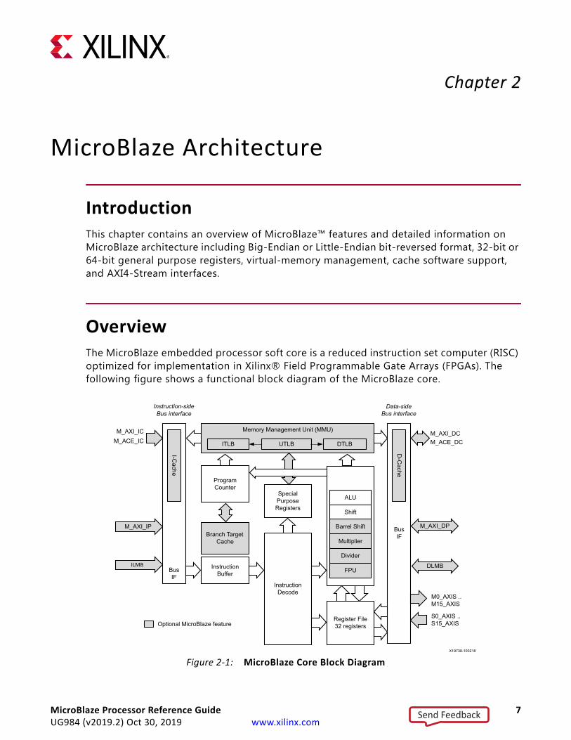
OverviewThe MicroBlaze embedded processor soft core is a reduced instruction set computer (RISC) optimized for implementation in Xilinx® Field Programmable Gate Arrays (FPGAs). The following figure shows a functional block diagram of the MicroBlaze core.
X-Ref Target - Figure 2-1
Figure 2-1: MicroBlaze Core Block Diagram
BusIF
I-Cache
Instruction Buffer
Instruction Buffer
Branch Target Cache
ProgramCounter
M_AXI_IC Memory Management Unit (MMU)
ITLB DTLBUTLB
BusIF
D-C
ache
M_AXI_DC
M_AXI_DP
DLMB
M0_AXIS .. M15_AXIS
S0_AXIS .. S15_AXIS
Special Purpose Registers
InstructionDecode
Register File32 registers
ALU
Shift
Barrel Shift
Multiplier
Divider
FPU
Instruction-sideBus interface
Data-sideBus interface
Optional MicroBlaze feature
M_AXI_IP
ILMB
M_ACE_DCM_ACE_IC
X19738-100218
MicroBlaze Processor Reference Guide 7UG984 (v2019.2) Oct 30, 2019 www.xilinx.com
Send Feedback

Chapter 2: MicroBlaze Architecture
FeaturesThe MicroBlaze soft core processor is highly configurable, allowing you to select a specific set of features required by your design.
The fixed feature set of the processor includes:
• Thirty-two 32-bit or 64-bit general purpose registers
• 32-bit instruction word with three operands and two addressing modes
• Default 32-bit address bus, extensible to 64 bits
• Single issue pipeline
In addition to these fixed features, the MicroBlaze processor is parameterized to allow selective enabling of additional functionality. Older (deprecated) versions of MicroBlaze support a subset of the optional features described in this manual. Only the latest (preferred) version of MicroBlaze (v11.0) supports all options.
RECOMMENDED: Xilinx recommends that all new designs use the latest preferred version of the MicroBlaze processor.
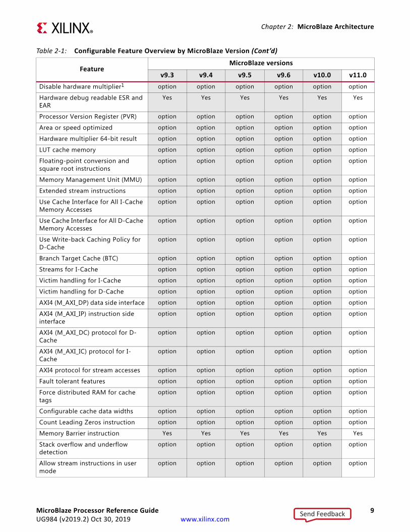
The following table provides an overview of the configurable features by MicroBlaze versions.
Table 2-1: Configurable Feature Overview by MicroBlaze Version
FeatureMicroBlaze versions
v9.3 v9.4 v9.5 v9.6 v10.0 v11.0Version Status deprecated deprecated deprecated deprecated deprecated preferred
Processor pipeline depth 3/5 3/5 3/5 3/5 3/5/8 3/5/8
Local Memory Bus (LMB) data side interface
option option option option option option
Local Memory Bus (LMB) instruction side interface
option option option option option option
Hardware barrel shifter option option option option option option
Hardware divider option option option option option option
Hardware debug logic option option option option option option
Stream link interfaces 0-16 AXI 0-16 AXI 0-16 AXI 0-16 AXI 0-16 AXI 0-16 AXI
Machine status set and clear instructions
option option option option option option
Cache line word length 4, 8 4, 8 4, 8, 16 4, 8, 16 4, 8, 16 4, 8, 16
Hardware exception support option option option option option option
Pattern compare instructions option option option option option option
Floating-point unit (FPU) option option option option option option
MicroBlaze Processor Reference Guide 8UG984 (v2019.2) Oct 30, 2019 www.xilinx.com
Send Feedback
Chapter 2: MicroBlaze Architecture
Disable hardware multiplier1 option option option option option option
Hardware debug readable ESR and EAR
Yes Yes Yes Yes Yes Yes
Processor Version Register (PVR) option option option option option option
Area or speed optimized option option option option option option
Hardware multiplier 64-bit result option option option option option option
LUT cache memory option option option option option option
Floating-point conversion and square root instructions
option option option option option option
Memory Management Unit (MMU) option option option option option option
Extended stream instructions option option option option option option
Use Cache Interface for All I-Cache Memory Accesses
option option option option option option
Use Cache Interface for All D-Cache Memory Accesses
option option option option option option
Use Write-back Caching Policy for D-Cache
option option option option option option
Branch Target Cache (BTC) option option option option option option
Streams for I-Cache option option option option option option
Victim handling for I-Cache option option option option option option
Victim handling for D-Cache option option option option option option
AXI4 (M_AXI_DP) data side interface option option option option option option
AXI4 (M_AXI_IP) instruction side interface
option option option option option option
AXI4 (M_AXI_DC) protocol for D-Cache
option option option option option option
AXI4 (M_AXI_IC) protocol for I-Cache
option option option option option option
AXI4 protocol for stream accesses option option option option option option
Fault tolerant features option option option option option option
Force distributed RAM for cache tags
option option option option option option
Configurable cache data widths option option option option option option
Count Leading Zeros instruction option option option option option option
Memory Barrier instruction Yes Yes Yes Yes Yes Yes
Stack overflow and underflow detection
option option option option option option
Allow stream instructions in user mode
option option option option option option
Table 2-1: Configurable Feature Overview by MicroBlaze Version (Cont’d)
FeatureMicroBlaze versions
v9.3 v9.4 v9.5 v9.6 v10.0 v11.0
MicroBlaze Processor Reference Guide 9UG984 (v2019.2) Oct 30, 2019 www.xilinx.com
Send Feedback

Chapter 2: MicroBlaze Architecture
Lockstep support option option option option option option
Configurable use of FPGA primitives
option option option option option option
Low-latency interrupt mode option option option option option option
Swap instructions option option option option option option
Sleep mode and sleep instruction Yes Yes Yes Yes Yes Yes
Relocatable base vectors option option option option option option
ACE (M_ACE_DC) protocol for D-Cache
option option option option option option
ACE (M_ACE_IC) protocol for I-Cache
option option option option option option
Extended debug: performance monitoring, program trace, non-intrusive profiling
option option option option option option
Reset mode: enter sleep or debug halt at reset
option option option option option option
Extended debug: external program trace
option option option option option
Extended data addressing option option option
Pipeline pause functionality Yes Yes Yes
Hibernate and suspend instructions Yes Yes Yes
Non-secure mode Yes Yes Yes
Bit field instructions2 option option
Parallel debug interface option option
MMU Physical Address Extension option option
64-bit mode option1. Used for saving DSP48E primitives.2. Bit field instructions are available when C_USE_BARREL = 1.
Table 2-1: Configurable Feature Overview by MicroBlaze Version (Cont’d)
FeatureMicroBlaze versions
v9.3 v9.4 v9.5 v9.6 v10.0 v11.0
MicroBlaze Processor Reference Guide 10UG984 (v2019.2) Oct 30, 2019 www.xilinx.com
Send Feedback

Chapter 2: MicroBlaze Architecture
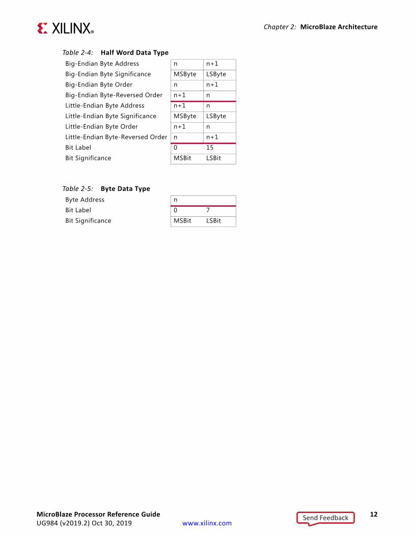
Data Types and EndiannessThe MicroBlaze processor uses Big-Endian or Little-Endian format to represent data, depending on the selected endianness. The parameter C_ENDIANNESS is set to 1 (little-endian) by default.
The hardware supported data types for 32-bit MicroBlaze are word, half word, and byte. With 64-bit MicroBlaze the data types long and double are also available in hardware.
When using the reversed load and store instructions LHUR, LWR, LLR, SHR, SWR and SLR, the bytes in the data are reversed, as indicated by the byte-reversed order.
The following tables show the bit and byte organization for each type.
Table 2-2: Long Data Type (only 64-bit MicroBlaze)
Big-Endian Byte Address n n+1 n+2 n+3 n+4 n+5 n+6 n+7
Big-Endian Byte Significance MSByte LSByte
Big-Endian Byte Order n n+1 n+2 n+3 n+4 n+5 n+6 n+7
Big-Endian Byte-Reversed Order n+7 n+6 n+5 n+4 n+3 n+2 n+1 n
Little-Endian Byte Address n+7 n+6 n+5 n+4 n+3 n+2 n+1 n
Little-Endian Byte Significance MSByte LSByte
Little-Endian Byte Order n+7 n+6 n+5 n+4 n+3 n+2 n+1 n
Little-Endian Byte-Reversed Order n n+1 n+2 n+3 n+4 n+5 n+6 n+7
Bit Label 0 63
Bit Significance MSBit LSBit
Table 2-3: Word Data TypeBig-Endian Byte Address n n+1 n+2 n+3
Big-Endian Byte Significance MSByte LSByte
Big-Endian Byte Order n n+1 n+2 n+3
Big-Endian Byte-Reversed Order n+3 n+2 n+1 n
Little-Endian Byte Address n+3 n+2 n+1 n
Little-Endian Byte Significance MSByte LSByte
Little-Endian Byte Order n+3 n+2 n+1 n
Little-Endian Byte-Reversed Order n n+1 n+2 n+3
Bit Label 0 31
Bit Significance MSBit LSBit
MicroBlaze Processor Reference Guide 11UG984 (v2019.2) Oct 30, 2019 www.xilinx.com
Send Feedback
Chapter 2: MicroBlaze Architecture
Table 2-4: Half Word Data TypeBig-Endian Byte Address n n+1
Big-Endian Byte Significance MSByte LSByte
Big-Endian Byte Order n n+1
Big-Endian Byte-Reversed Order n+1 n
Little-Endian Byte Address n+1 n
Little-Endian Byte Significance MSByte LSByte
Little-Endian Byte Order n+1 n
Little-Endian Byte-Reversed Order n n+1
Bit Label 0 15
Bit Significance MSBit LSBit
Table 2-5: Byte Data Type Byte Address n
Bit Label 0 7
Bit Significance MSBit LSBit
MicroBlaze Processor Reference Guide 12UG984 (v2019.2) Oct 30, 2019 www.xilinx.com
Send Feedback
Chapter 2: MicroBlaze Architecture
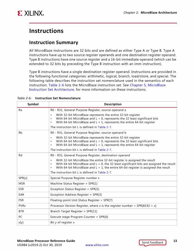
Instructions
Instruction SummaryAll MicroBlaze instructions are 32 bits and are defined as either Type A or Type B. Type A instructions have up to two source register operands and one destination register operand. Type B instructions have one source register and a 16-bit immediate operand (which can be extended to 32 bits by preceding the Type B instruction with an imm instruction).
Type B instructions have a single destination register operand. Instructions are provided in the following functional categories: arithmetic, logical, branch, load/store, and special. The following table describes the instruction set nomenclature used in the semantics of each instruction. Table 2-6 lists the MicroBlaze instruction set. See Chapter 5, MicroBlaze Instruction Set Architecture, for more information on these instructions.
Table 2-6: Instruction Set Nomenclature
Symbol Description
Ra R0 - R31, General Purpose Register, source operand a
• With 32-bit MicroBlaze represents the entire 32-bit register• With 64-bit MicroBlaze and L = 0, represents the 32 least significant bits• With 64-bit MicroBlaze and L = 1, represents the entire 64-bit register
The instruction bit L is defined in Table 2-7.
Rb R0 - R31, General Purpose Register, source operand b
• With 32-bit MicroBlaze represents the entire 32-bit register• With 64-bit MicroBlaze and L = 0, represents the 32 least significant bits• With 64-bit MicroBlaze and L = 1, represents the entire 64-bit register
The instruction bit L is defined in Table 2-7.
Rd R0 - R31, General Purpose Register, destination operand
• With 32-bit MicroBlaze the entire 32-bit register is assigned the result• With 64-bit MicroBlaze and L = 0, the 32 least significant bits are assigned the result• With 64-bit MicroBlaze and L = 1, the entire 64-bit register is assigned the result
The instruction bit L is defined in Table 2-7.
SPR[x] Special Purpose Register number x
MSR Machine Status Register = SPR[1]
ESR Exception Status Register = SPR[5]
EAR Exception Address Register = SPR[3]
FSR Floating-point Unit Status Register = SPR[7]
PVRx Processor Version Register, where x is the register number = SPR[8192 + x]
BTR Branch Target Register = SPR[11]
PC Execute stage Program Counter = SPR[0]
x[y] Bit y of register x
MicroBlaze Processor Reference Guide 13UG984 (v2019.2) Oct 30, 2019 www.xilinx.com
Send Feedback

Chapter 2: MicroBlaze Architecture
x[y:z] Bit range y to z of register x
x Bit inverted value of register x
Imm 16 bit immediate value
Immx x bit immediate value
FSLx 4 bit AXI4-Stream port designator, where x is the port number
C Carry flag, MSR[29]
Sa Special Purpose Register, source operand
Sd Special Purpose Register, destination operand
s(x) Sign extend argument x to 32-bit or 64-bit value
*Addr Memory contents at location Addr (data-size aligned)
:= Assignment operator
= Equality comparison
!= Inequality comparison
> Greater than comparison
>= Greater than or equal comparison
< Less than comparison
<= Less than or equal comparison
+ Arithmetic add
* Arithmetic multiply
/ Arithmetic divide
>> x Bit shift right x bits
<< x Bit shift left x bits
and Logic AND
or Logic OR
xor Logic exclusive OR
op1 if cond else op2 Perform op1 if condition cond is true, else perform op2
& Concatenate. For example “0000100 & Imm7” is the concatenation of the fixed field “0000100” and a 7 bit immediate value.
signed Operation performed on signed integer data type. All arithmetic operations are performed on signed word operands, unless otherwise specified
unsigned Operation performed on unsigned integer data type
float Operation performed on floating-point data type
clz(r) Count leading zeros
Table 2-6: Instruction Set Nomenclature (Cont’d)
Symbol Description
MicroBlaze Processor Reference Guide 14UG984 (v2019.2) Oct 30, 2019 www.xilinx.com
Send Feedback

Chapter 2: MicroBlaze Architecture
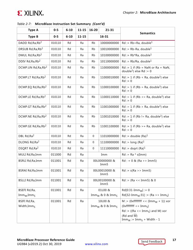
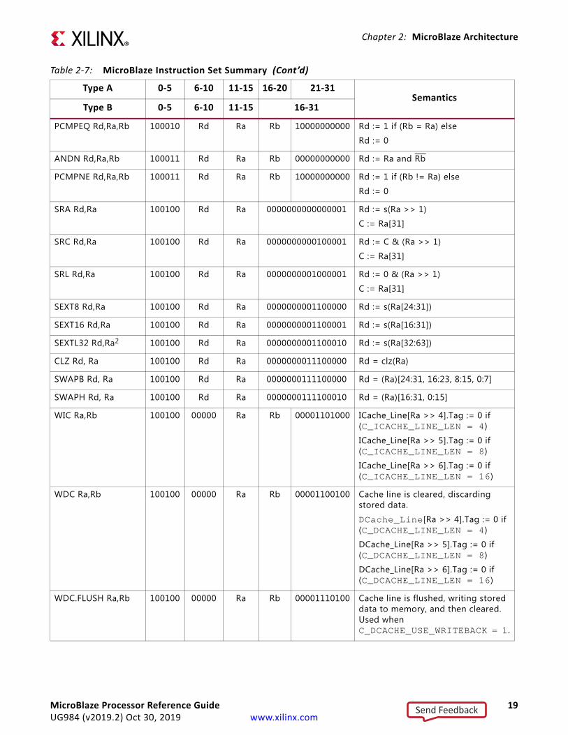
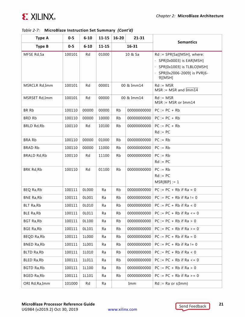
Table 2-7: MicroBlaze Instruction Set Summary
Type A 0-5 6-10 11-15 16-20 21-31Semantics
Type B 0-5 6-10 11-15 16-31
ADD Rd,Ra,Rb 000000 Rd Ra Rb 00L00000000 Rd := Rb + Ra
RSUB Rd,Ra,Rb 000001 Rd Ra Rb 00L00000000 Rd := Rb + Ra + 1
ADDC Rd,Ra,Rb 000010 Rd Ra Rb 00L00000000 Rd := Rb + Ra + C
RSUBC Rd,Ra,Rb 000011 Rd Ra Rb 00L00000000 Rd := Rb + Ra + C
ADDK Rd,Ra,Rb 000100 Rd Ra Rb 00L00000000 Rd := Rb + Ra
RSUBK Rd,Ra,Rb 000101 Rd Ra Rb 00L00000000 Rd := Rb + Ra + 1
CMP Rd,Ra,Rb 000101 Rd Ra Rb 00L00000001 Rd := Rb + Ra + 1
Rd[0] := 0 if (Rb >= Ra) else
Rd[0] := 1
CMPU Rd,Ra,Rb 000101 Rd Ra Rb 00L00000011 Rd := Rb + Ra + 1 (unsigned) Rd[0] := 0 if (Rb >= Ra, unsigned) else Rd[0] := 1
ADDKC Rd,Ra,Rb 000110 Rd Ra Rb 00L00000000 Rd := Rb + Ra + C
RSUBKC Rd,Ra,Rb 000111 Rd Ra Rb 00L00000000 Rd := Rb + Ra + C
ADDI Rd,Ra,Imm 001000 Rd Ra Imm Rd := s(Imm) + Ra
RSUBI Rd,Ra,Imm 001001 Rd Ra Imm Rd := s(Imm) + Ra + 1
ADDIC Rd,Ra,Imm 001010 Rd Ra Imm Rd := s(Imm) + Ra + C
RSUBIC Rd,Ra,Imm 001011 Rd Ra Imm Rd := s(Imm) + Ra + C
ADDIK Rd,Ra,Imm 001100 Rd Ra Imm Rd := s(Imm) + Ra
RSUBIK Rd,Ra,Imm 001101 Rd Ra Imm Rd := s(Imm) + Ra + 1
ADDIKC Rd,Ra,Imm 001110 Rd Ra Imm Rd := s(Imm) + Ra + C
RSUBIKC Rd,Ra,Imm 001111 Rd Ra Imm Rd := s(Imm) + Ra + C
MUL Rd,Ra,Rb 010000 Rd Ra Rb 00000000000 Rd := Ra * Rb
MULH Rd,Ra,Rb 010000 Rd Ra Rb 00000000001 Rd := (Ra * Rb) >> 32 (signed)
MULHU Rd,Ra,Rb 010000 Rd Ra Rb 00000000011 Rd := (Ra * Rb) >> 32 (unsigned)
MULHSU Rd,Ra,Rb 010000 Rd Ra Rb 00000000010 Rd := (Ra, signed * Rb, unsigned) >> 32 (signed)
BSRL Rd,Ra,Rb 010001 Rd Ra Rb 00L00000000 Rd := 0 & (Ra >> Rb)
BSRA Rd,Ra,Rb 010001 Rd Ra Rb 01L00000000 Rd := s(Ra >> Rb)
BSLL Rd,Ra,Rb 010001 Rd Ra Rb 10L00000000 Rd := (Ra << Rb) & 0
IDIV Rd,Ra,Rb 010010 Rd Ra Rb 00000000000 Rd := Rb/Ra
MicroBlaze Processor Reference Guide 15UG984 (v2019.2) Oct 30, 2019 www.xilinx.com
Send Feedback

Chapter 2: MicroBlaze Architecture
IDIVU Rd,Ra,Rb 010010 Rd Ra Rb 00000000010 Rd := Rb/Ra, unsigned
TNEAGETD Rd,Rb 010011 Rd 00000 Rb 0N0TAE
00000
Rd := FSL Rb[28:31] (data read)
MSR[FSL] := 1 if (FSL_S_Control = 1)
MSR[C] := not FSL_S_Exists if N = 1
TNAPUTD Ra,Rb 010011 00000 Ra Rb 0N0TA0
00000
FSL Rb[28:31] := Ra (data write)
MSR[C] := FSL_M_Full if N = 1
TNECAGETD Rd,Rb 010011 Rd 00000 Rb 0N1TAE
00000
Rd := FSL Rb[28:31] (control read)
MSR[FSL] := 1 if (FSL_S_Control = 0)
MSR[C] := not FSL_S_Exists if N = 1
TNCAPUTD Ra,Rb 010011 00000 Ra Rb 0N1TA000000
FSL Rb[28:31] := Ra (control write)
MSR[C] := FSL_M_Full if N = 1
FADD Rd,Ra,Rb 010110 Rd Ra Rb 00000000000 Rd := Rb+Ra, float1
FRSUB Rd,Ra,Rb 010110 Rd Ra Rb 00010000000 Rd := Rb-Ra, float1
FMUL Rd,Ra,Rb 010110 Rd Ra Rb 00100000000 Rd := Rb*Ra, float1
FDIV Rd,Ra,Rb 010110 Rd Ra Rb 00110000000 Rd := Rb/Ra, float1
FCMP.UN Rd,Ra,Rb 010110 Rd Ra Rb 01000000000 Rd := 1 if (Rb = NaN or Ra = NaN, float1) else
Rd := 0
FCMP.LT Rd,Ra,Rb 010110 Rd Ra Rb 01000010000 Rd := 1 if (Rb < Ra, float1) else
Rd := 0
FCMP.EQ Rd,Ra,Rb 010110 Rd Ra Rb 01000100000 Rd := 1 if (Rb = Ra, float1) else
Rd := 0
FCMP.LE Rd,Ra,Rb 010110 Rd Ra Rb 01000110000 Rd := 1 if (Rb <= Ra, float1) else
Rd := 0
FCMP.GT Rd,Ra,Rb 010110 Rd Ra Rb 01001000000 Rd := 1 if (Rb > Ra, float1) else
Rd := 0
FCMP.NE Rd,Ra,Rb 010110 Rd Ra Rb 01001010000 Rd := 1 if (Rb != Ra, float1) else
Rd := 0
FCMP.GE Rd,Ra,Rb 010110 Rd Ra Rb 01001100000 Rd := 1 if (Rb >= Ra, float1) else
Rd := 0
FLT Rd,Ra 010110 Rd Ra 0 01010000000 Rd := float (Ra)1
FINT Rd,Ra 010110 Rd Ra 0 01100000000 Rd := int (Ra)1
FSQRT Rd,Ra 010110 Rd Ra 0 01110000000 Rd := sqrt (Ra)1
Table 2-7: MicroBlaze Instruction Set Summary (Cont’d)
Type A 0-5 6-10 11-15 16-20 21-31Semantics
Type B 0-5 6-10 11-15 16-31
MicroBlaze Processor Reference Guide 16UG984 (v2019.2) Oct 30, 2019 www.xilinx.com
Send Feedback
Chapter 2: MicroBlaze Architecture
DADD Rd,Ra,Rb2 010110 Rd Ra Rb 10000000000 Rd := Rb+Ra, double1
DRSUB Rd,Ra,Rb2 010110 Rd Ra Rb 10010000000 Rd := Rb-Ra, double1
DMUL Rd,Ra,Rb2 010110 Rd Ra Rb 10100000000 Rd := Rb*Ra, double1
DDIV Rd,Ra,Rb2 010110 Rd Ra Rb 10110000000 Rd := Rb/Ra, double1
DCMP.UN Rd,Ra,Rb2 010110 Rd Ra Rb 11000000000 Rd := 1 if (Rb = NaN or Ra = NaN, double1) else Rd := 0
DCMP.LT Rd,Ra,Rb2 010110 Rd Ra Rb 11000010000 Rd := 1 if (Rb < Ra, double1) else Rd := 0
DCMP.EQ Rd,Ra,Rb2 010110 Rd Ra Rb 11000100000 Rd := 1 if (Rb = Ra, double1) else Rd := 0
DCMP.LE Rd,Ra,Rb2 010110 Rd Ra Rb 11000110000 Rd := 1 if (Rb <= Ra, double1) else Rd := 0
DCMP.GT Rd,Ra,Rb2 010110 Rd Ra Rb 11001000000 Rd := 1 if (Rb > Ra, double1) else Rd := 0
DCMP.NE Rd,Ra,Rb2 010110 Rd Ra Rb 11001010000 Rd := 1 if (Rb != Ra, double1) else Rd := 0
DCMP.GE Rd,Ra,Rb2 010110 Rd Ra Rb 11001100000 Rd := 1 if (Rb >= Ra, double1) else Rd := 0
DBL Rd,Ra2 010110 Rd Ra 0 11010000000 Rd := double (Ra)1
DLONG Rd,Ra2 010110 Rd Ra 0 11100000000 Rd := long (Ra)1
DSQRT Rd,Ra2 010110 Rd Ra 0 11110000000 Rd := dsqrt (Ra)1
MULI Rd,Ra,Imm 011000 Rd Ra Imm Rd := Ra * s(Imm)
BSRLI Rd,Ra,Imm 011001 Rd Ra 00L00000000 & Imm5
Rd : = 0 & (Ra >> Imm5)
BSRAI Rd,Ra,Imm 011001 Rd Ra 00L00010000 & Imm5
Rd := s(Ra >> Imm5)
BSLLI Rd,Ra,Imm 011001 Rd Ra 00L00100000 & Imm5
Rd := (Ra << Imm5) & 0
BSEFI Rd,Ra,
ImmW,ImmS
011001 Rd Ra 01L00 &
ImmW & 0 & ImmS
Rd[0:31-ImmW] := 0
Rd[32-ImmW:31] := (Ra >> ImmS)
BSIFI Rd,Ra,
Width,ImmS
011001 Rd Ra 10L00 &
ImmW & 0 & ImmS
M := (0xffffffff << (ImmW + 1)) xor
(0xffffffff << ImmS)
Rd := ((Ra << ImmS) and M) xor
(Rd and M) ImmW := ImmS + Width - 1
Table 2-7: MicroBlaze Instruction Set Summary (Cont’d)
Type A 0-5 6-10 11-15 16-20 21-31Semantics
Type B 0-5 6-10 11-15 16-31
MicroBlaze Processor Reference Guide 17UG984 (v2019.2) Oct 30, 2019 www.xilinx.com
Send Feedback

Chapter 2: MicroBlaze Architecture
ADDLI Rd,Imm2 011010 Rd 00000 Imm Rd[0:63] := s(Imm) + Rd[0:63]
RSUBLI Rd,Imm2 011010 Rd 00001 Imm Rd[0:63] := s(Imm) + Rd[0:63]
ADDLIC Rd,Imm2 011010 Rd 00010 Imm Rd[0:63] := s(Imm) + Rd[0:63] + C
RSUBLIC Rd,Imm2 011010 Rd 00011 Imm Rd[0:63] := s(Imm) + Rd[0:63] + C
ADDLIK Rd,Imm2 011010 Rd 00100 Imm Rd[0:63] := s(Imm) + Rd[0:63]
RSUBLIK Rd,Imm2 011010 Rd 00101 Imm Rd[0:63] := s(Imm) + Rd[0:63]
ADDLIKC Rd,Imm2 011010 Rd 00110 Imm Rd[0:63] := s(Imm) + Rd[0:63] + C
RSUBLIKC Rd,Imm2 011010 Rd 00111 Imm Rd[0:63] := s(Imm) + Rd[0:63] + C
ORLI Rd,Imm2 011010 Rd 10000 Imm Rd[0:63] := s(Imm) or Rd[0:63]
ANDLI Rd,Imm2 011010 Rd 10001 Imm Rd[0:63] := s(Imm) and Rd[0:63]
XORLI Rd,Imm2 011010 Rd 10010 Imm Rd[0:63] := s(Imm) xor Rd[0:63]
ANDNLI Rd,Imm2 011010 Rd 10011 Imm Rd[0:63] := s(Imm) and Rd[0:63]
TNEAGET Rd,FSLx 011011 Rd 00000 0N0TAE000000 & FSLx
Rd := FSLx (data read, blocking if N = 0)
MSR[FSL] := 1 if (FSLx_S_Control = 1)
MSR[C] := not FSLx_S_Exists if N = 1
TNAPUT Ra,FSLx 011011 00000 Ra 1N0TA0000000 & FSLx
FSLx := Ra (data write, block if N = 0)
MSR[C] := FSLx_M_Full if N = 1
TNECAGET Rd,FSLx 011011 Rd 00000 0N1TAE000000 & FSLx
Rd := FSLx (control read, block if N = 0)
MSR[FSL] := 1 if (FSLx_S_Control = 0)
MSR[C] := not FSLx_S_Exists if N = 1
TNCAPUT Ra,FSLx 011011 00000 Ra 1N1TA0000000 & FSLx
FSLx := Ra (control write, block if N = 0)
MSR[C] := FSLx_M_Full if N = 1
OR Rd,Ra,Rb 100000 Rd Ra Rb 00000000000 Rd := Ra or Rb
PCMPBF Rd,Ra,Rb 100000 Rd Ra Rb 10000000000 Rd := 1 if (Rb[0:7] = Ra[0:7]) else
Rd := 2 if (Rb[8:15] = Ra[8:15]) else
Rd := 3 if (Rb[16:23] = Ra[16:23]) else
Rd := 4 if (Rb[24:31] = Ra[24:31]) else
Rd := 0
AND Rd,Ra,Rb 100001 Rd Ra Rb 00000000000 Rd := Ra and Rb
XOR Rd,Ra,Rb 100010 Rd Ra Rb 00000000000 Rd := Ra xor Rb
Table 2-7: MicroBlaze Instruction Set Summary (Cont’d)
Type A 0-5 6-10 11-15 16-20 21-31Semantics
Type B 0-5 6-10 11-15 16-31
MicroBlaze Processor Reference Guide 18UG984 (v2019.2) Oct 30, 2019 www.xilinx.com
Send Feedback
Chapter 2: MicroBlaze Architecture
PCMPEQ Rd,Ra,Rb 100010 Rd Ra Rb 10000000000 Rd := 1 if (Rb = Ra) else
Rd := 0
ANDN Rd,Ra,Rb 100011 Rd Ra Rb 00000000000 Rd := Ra and Rb
PCMPNE Rd,Ra,Rb 100011 Rd Ra Rb 10000000000 Rd := 1 if (Rb != Ra) else
Rd := 0
SRA Rd,Ra 100100 Rd Ra 0000000000000001 Rd := s(Ra >> 1)
C := Ra[31]
SRC Rd,Ra 100100 Rd Ra 0000000000100001 Rd := C & (Ra >> 1)
C := Ra[31]
SRL Rd,Ra 100100 Rd Ra 0000000001000001 Rd := 0 & (Ra >> 1)
C := Ra[31]
SEXT8 Rd,Ra 100100 Rd Ra 0000000001100000 Rd := s(Ra[24:31])
SEXT16 Rd,Ra 100100 Rd Ra 0000000001100001 Rd := s(Ra[16:31])
SEXTL32 Rd,Ra2 100100 Rd Ra 0000000001100010 Rd := s(Ra[32:63])
CLZ Rd, Ra 100100 Rd Ra 0000000011100000 Rd = clz(Ra)
SWAPB Rd, Ra 100100 Rd Ra 0000000111100000 Rd = (Ra)[24:31, 16:23, 8:15, 0:7]
SWAPH Rd, Ra 100100 Rd Ra 0000000111100010 Rd = (Ra)[16:31, 0:15]
WIC Ra,Rb 100100 00000 Ra Rb 00001101000 ICache_Line[Ra >> 4].Tag := 0 if (C_ICACHE_LINE_LEN = 4)
ICache_Line[Ra >> 5].Tag := 0 if (C_ICACHE_LINE_LEN = 8)
ICache_Line[Ra >> 6].Tag := 0 if (C_ICACHE_LINE_LEN = 16)
WDC Ra,Rb 100100 00000 Ra Rb 00001100100 Cache line is cleared, discarding stored data.
DCache_Line[Ra >> 4].Tag := 0 if (C_DCACHE_LINE_LEN = 4)
DCache_Line[Ra >> 5].Tag := 0 if (C_DCACHE_LINE_LEN = 8)
DCache_Line[Ra >> 6].Tag := 0 if (C_DCACHE_LINE_LEN = 16)
WDC.FLUSH Ra,Rb 100100 00000 Ra Rb 00001110100 Cache line is flushed, writing stored data to memory, and then cleared. Used when C_DCACHE_USE_WRITEBACK = 1.
Table 2-7: MicroBlaze Instruction Set Summary (Cont’d)
Type A 0-5 6-10 11-15 16-20 21-31Semantics
Type B 0-5 6-10 11-15 16-31
MicroBlaze Processor Reference Guide 19UG984 (v2019.2) Oct 30, 2019 www.xilinx.com
Send Feedback

Chapter 2: MicroBlaze Architecture
WDC.CLEAR Ra,Rb 100100 00000 Ra Rb 00001100110 Cache line with matching address is cleared, discarding stored data. Used when C_DCACHE_USE_WRITEBACK = 1.
WDC.CLEAR.EA Ra,Rb
100100 00000 Ra Rb 00011100110 Cache line with matching extended address Ra & Rb is cleared. Used when C_DCACHE_USE_WRITEBACK = 1.
MTS Sd,Ra 100101 00000 Ra 11 & Sd SPR[Sd] := Ra, where:· SPR[0x0001] is MSR· SPR[0x0007] is FSR· SPR[0x0800] is SLR· SPR[0x0802] is SHR· SPR[0x1000] is PID· SPR[0x1001] is ZPR· SPR[0x1002] is TLBX· SPR[0x1003] is TLBLO[LSH]· SPR[0x1004] is TLBHI· SPR[0x1005] is TLBSX
MTSE Sd,Ra 100101 01000 Ra 11 & Sd SPR[Sd} := Ra, where:
· SPR[0x1003] is TLBLO[MSH]
MFS Rd,Sa 100101 Rd 00000 10 & Sa Rd := SPR[Sa], where:
· SPR[0x0000] is PC
· SPR[0x0001] is MSR
· SPR[0x0003] is EAR[LSH]
· SPR[0x0005] is ESR
· SPR[0x0007] is FSR
· SPR[0x000B] is BTR
· SPR[0x000D] is EDR
· SPR[0x0800] is SLR
· SPR[0x0802] is SHR
· SPR[0x1000] is PID
· SPR[0x1001] is ZPR
· SPR[0x1002] is TLBX
· SPR[0x1003] is TLBLO[LSH]
· SPR[0x1004] is TLBHI
· SPR[0x2000-200B] is PVR[0-12][LSH]
Table 2-7: MicroBlaze Instruction Set Summary (Cont’d)
Type A 0-5 6-10 11-15 16-20 21-31Semantics
Type B 0-5 6-10 11-15 16-31
MicroBlaze Processor Reference Guide 20UG984 (v2019.2) Oct 30, 2019 www.xilinx.com
Send Feedback
Chapter 2: MicroBlaze Architecture
MFSE Rd,Sa 100101 Rd 01000 10 & Sa Rd := SPR[Sa][MSH], where:
· SPR[0x0003] is EAR[MSH]
· SPR[0x1003] is TLBLO[MSH]
· SPR[0x2006-2009] is PVR[6-9][MSH]
MSRCLR Rd,Imm 100101 Rd 00001 00 & Imm14 Rd := MSR MSR := MSR and Imm14
MSRSET Rd,Imm 100101 Rd 00000 00 & Imm14 Rd := MSR MSR := MSR or Imm14
BR Rb 100110 00000 00000 Rb 00000000000 PC := PC + Rb
BRD Rb 100110 00000 10000 Rb 00000000000 PC := PC + Rb
BRLD Rd,Rb 100110 Rd 10100 Rb 00000000000 PC := PC + Rb
Rd := PC
BRA Rb 100110 00000 01000 Rb 00000000000 PC := Rb
BRAD Rb 100110 00000 11000 Rb 00000000000 PC := Rb
BRALD Rd,Rb 100110 Rd 11100 Rb 00000000000 PC := Rb
Rd := PC
BRK Rd,Rb 100110 Rd 01100 Rb 00000000000 PC := Rb
Rd := PC
MSR[BIP] := 1
BEQ Ra,Rb 100111 0L000 Ra Rb 00000000000 PC := PC + Rb if Ra = 0
BNE Ra,Rb 100111 0L001 Ra Rb 00000000000 PC := PC + Rb if Ra != 0
BLT Ra,Rb 100111 0L010 Ra Rb 00000000000 PC := PC + Rb if Ra < 0
BLE Ra,Rb 100111 0L011 Ra Rb 00000000000 PC := PC + Rb if Ra <= 0
BGT Ra,Rb 100111 0L100 Ra Rb 00000000000 PC := PC + Rb if Ra > 0
BGE Ra,Rb 100111 0L101 Ra Rb 00000000000 PC := PC + Rb if Ra >= 0
BEQD Ra,Rb 100111 1L000 Ra Rb 00000000000 PC := PC + Rb if Ra = 0
BNED Ra,Rb 100111 1L001 Ra Rb 00000000000 PC := PC + Rb if Ra != 0
BLTD Ra,Rb 100111 1L010 Ra Rb 00000000000 PC := PC + Rb if Ra < 0
BLED Ra,Rb 100111 1L011 Ra Rb 00000000000 PC := PC + Rb if Ra <= 0
BGTD Ra,Rb 100111 1L100 Ra Rb 00000000000 PC := PC + Rb if Ra > 0
BGED Ra,Rb 100111 1L101 Ra Rb 00000000000 PC := PC + Rb if Ra >= 0
ORI Rd,Ra,Imm 101000 Rd Ra Imm Rd := Ra or s(Imm)
Table 2-7: MicroBlaze Instruction Set Summary (Cont’d)
Type A 0-5 6-10 11-15 16-20 21-31Semantics
Type B 0-5 6-10 11-15 16-31
MicroBlaze Processor Reference Guide 21UG984 (v2019.2) Oct 30, 2019 www.xilinx.com
Send Feedback

Chapter 2: MicroBlaze Architecture
ANDI Rd,Ra,Imm 101001 Rd Ra Imm Rd := Ra and s(Imm)
XORI Rd,Ra,Imm 101010 Rd Ra Imm Rd := Ra xor s(Imm)
ANDNI Rd,Ra,Imm 101011 Rd Ra Imm Rd := Ra and s(Imm)
IMM Imm 101100 00000 00000 Imm Imm[0:15] := Imm
IMML Imm242 101100 10 Imm24 Imm[24:47] := Imm24
RTSD Ra,Imm 101101 10000 Ra Imm PC := Ra + s(Imm)
RTID Ra,Imm 101101 10001 Ra Imm PC := Ra + s(Imm)
MSR[IE] := 1
RTBD Ra,Imm 101101 10010 Ra Imm PC := Ra + s(Imm)
MSR[BIP] := 0
RTED Ra,Imm 101101 10100 Ra Imm PC := Ra + s(Imm)
MSR[EE] := 1, MSR[EIP] := 0
ESR := 0
BRI Imm 101110 00000 00000 Imm PC := PC + s(Imm)
MBAR Imm 101110 Imm 00010 0000000000000100 PC := PC + 4; Wait for memory accesses.
BRID Imm 101110 00000 10000 Imm PC := PC + s(Imm)
BRLID Rd,Imm 101110 Rd 10100 Imm PC := PC + s(Imm)
Rd := PC
BRAI Imm 101110 00000 01000 Imm PC := s(Imm)
BRAID Imm 101110 00000 11000 Imm PC := s(Imm)
BRALID Rd,Imm 101110 Rd 11100 Imm PC := s(Imm)
Rd := PC
BRKI Rd,Imm 101110 Rd 01100 Imm PC := s(Imm)
Rd := PC MSR[BIP] := 1
BEQI Ra,Imm 101111 0L000 Ra Imm PC := PC + s(Imm) if Ra = 0
BNEI Ra,Imm 101111 0L001 Ra Imm PC := PC + s(Imm) if Ra != 0
BLTI Ra,Imm 101111 0L010 Ra Imm PC := PC + s(Imm) if Ra < 0
BLEI Ra,Imm 101111 0L011 Ra Imm PC := PC + s(Imm) if Ra <= 0
BGTI Ra,Imm 101111 0L100 Ra Imm PC := PC + s(Imm) if Ra > 0
BGEI Ra,Imm 101111 0L101 Ra Imm PC := PC + s(Imm) if Ra >= 0
Table 2-7: MicroBlaze Instruction Set Summary (Cont’d)
Type A 0-5 6-10 11-15 16-20 21-31Semantics
Type B 0-5 6-10 11-15 16-31
MicroBlaze Processor Reference Guide 22UG984 (v2019.2) Oct 30, 2019 www.xilinx.com
Send Feedback

Chapter 2: MicroBlaze Architecture
BEQID Ra,Imm 101111 1L000 Ra Imm PC := PC + s(Imm) if Ra = 0
BNEID Ra,Imm 101111 1L001 Ra Imm PC := PC + s(Imm) if Ra != 0
BLTID Ra,Imm 101111 1L010 Ra Imm PC := PC + s(Imm) if Ra < 0
BLEID Ra,Imm 101111 1L011 Ra Imm PC := PC + s(Imm) if Ra <= 0
BGTID Ra,Imm 101111 1L100 Ra Imm PC := PC + s(Imm) if Ra > 0
BGEID Ra,Imm 101111 1L101 Ra Imm PC := PC + s(Imm) if Ra >= 0
LBU Rd,Ra,Rb
LBUR Rd,Ra,Rb
110000 Rd Ra Rb 00000000000
01000000000
Addr := Ra + Rb
Rd[0:23] := 0
Rd[24:31] := *Addr[0:7]
LBUEA Rd,Ra,Rb 110000 Rd Ra Rb 00010000000 Addr := Ra & Rb
Rd[0:23] := 0
Rd[24:31] := *Addr[0:7]
LHU Rd,Ra,Rb
LHUR Rd,Ra,Rb
110001 Rd Ra Rb 00000000000
01000000000
Addr := Ra + Rb
Rd[0:15] := 0
Rd[16:31] := *Addr[0:15]
LHUEA Rd,Ra,Rb 110001 Rd Ra Rb 00010000000 Addr := Ra & Rb
Rd[0:15] := 0
Rd[16:31] := *Addr[0:15]
LW Rd,Ra,Rb
LWR Rd,Ra,Rb
110010 Rd Ra Rb 00000000000 01000000000
Addr := Ra + Rb
Rd := *Addr
LWX Rd,Ra,Rb 110010 Rd Ra Rb 10000000000 Addr := Ra + Rb
Rd := *Addr Reservation := 1
LWEA Rd,Ra,Rb 110010 Rd Ra Rb 00010000000 Addr := Ra & Rb
Rd := *Addr
LL Rd,Ra,Rb2
LLR Rd,Ra,Rb2110010 Rd Ra Rb 00100000000
01100000000Addr := Ra[0:63] + Rb[0:63] Rd[0:63] := *Addr[0:63]
SB Rd,Ra,Rb
SBR Rd,Ra,Rb
110100 Rd Ra Rb 00000000000
01000000000
Addr := Ra + Rb
*Addr[0:8] := Rd[24:31]
SBEA Rd,Ra,Rb 110100 Rd Ra Rb 00010000000 Addr := Ra & Rb
*Addr[0:8] := Rd[24:31]
SH Rd,Ra,Rb
SHR Rd,Ra,Rb
110101 Rd Ra Rb 00000000000
01000000000
Addr := Ra + Rb
*Addr[0:16] := Rd[16:31]
Table 2-7: MicroBlaze Instruction Set Summary (Cont’d)
Type A 0-5 6-10 11-15 16-20 21-31Semantics
Type B 0-5 6-10 11-15 16-31
MicroBlaze Processor Reference Guide 23UG984 (v2019.2) Oct 30, 2019 www.xilinx.com
Send Feedback

Chapter 2: MicroBlaze Architecture
SHEA Rd,Ra,Rb 110101 Rd Ra Rb 00010000000 Addr := Ra & Rb
*Addr[0:16] := Rd[16:31]
SW Rd,Ra,Rb
SWR Rd,Ra,Rb
110110 Rd Ra Rb 00000000000 01000000000
Addr := Ra + Rb
*Addr := Rd
SWX Rd,Ra,Rb 110110 Rd Ra Rb 10000000000 Addr := Ra + Rb
*Addr := Rd if Reservation = 1
Reservation := 0
SWEA Rd,Ra,Rb 110110 Rd Ra Rb 00010000000 Addr := Ra & Rb
*Addr := Rd
SL Rd,Ra,Rb2
SLR Rd,Ra,Rb2110110 Rd Ra Rb 00100000000
01100000000Addr := Ra[0:63] + Rb[0:63] *Addr[0:63] := Rd[0:63]
LBUI Rd,Ra,Imm 111000 Rd Ra Imm Addr := Ra + s(Imm)
Rd[0:23] := 0
Rd[24:31] := *Addr[0:7]
LHUI Rd,Ra,Imm 111001 Rd Ra Imm Addr := Ra + s(Imm)
Rd[0:15] := 0 Rd[16:31] := *Addr[0:15]
LWI Rd,Ra,Imm 111010 Rd Ra Imm Addr := Ra + s(Imm)
Rd := *Addr
LLI Rd,Ra,Imm2 111011 Rd Ra Imm Addr := Ra[0:63] + s(Imm)
Rd[0:63] := *Addr[0:63]
SBI Rd,Ra,Imm 111100 Rd Ra Imm Addr := Ra + s(Imm)
*Addr[0:7] := Rd[24:31]
SHI Rd,Ra,Imm 111101 Rd Ra Imm Addr := Ra + s(Imm)
*Addr[0:15] := Rd[16:31]
SWI Rd,Ra,Imm 111110 Rd Ra Imm Addr := Ra + s(Imm)
*Addr := Rd
SLI Rd,Ra,Imm2 111111 Rd Ra Imm Addr := Ra[0:63] + s(Imm)
*Addr[0:63] := Rd[0:63]
1. Due to the many different corner cases involved in floating-point arithmetic, only the normal behavior is described. A full description of the behavior can be found in Chapter 5, “MicroBlaze Instruction Set Architecture.”
2. Only available with 64-bit MicroBlaze.
Table 2-7: MicroBlaze Instruction Set Summary (Cont’d)
Type A 0-5 6-10 11-15 16-20 21-31Semantics
Type B 0-5 6-10 11-15 16-31
MicroBlaze Processor Reference Guide 24UG984 (v2019.2) Oct 30, 2019 www.xilinx.com
Send Feedback

Chapter 2: MicroBlaze Architecture
Semaphore SynchronizationThe LWX and SWX instructions are used to implement common semaphore operations, including test and set, compare and swap, exchange memory, and fetch and add. They are also used to implement spinlocks.
These instructions are typically used by system programs and are called by application programs as needed.
Generally, a program uses LWX to load a semaphore from memory, causing the reservation to be set (the processor maintains the reservation internally). The program can compute a result based on the semaphore value and conditionally store the result back to the same memory location using the SWX instruction. The conditional store is performed based on the existence of the reservation established by the preceding LWX instruction. If the reservation exists when the store is executed, the store is performed and MSR[C] is cleared to 0. If the reservation does not exist when the store is executed, the target memory location is not modified and MSR[C] is set to 1.
If the store is successful, the sequence of instructions from the semaphore load to the semaphore store appear to be executed atomically—no other device modified the semaphore location between the read and the update. Other devices can read from the semaphore location during the operation.
For a semaphore operation to work properly, the LWX instruction must be paired with an SWX instruction, and both must specify identical addresses.
The reservation granularity in MicroBlaze is a word. For both instructions, the address must be word aligned. No unaligned exceptions are generated for these instructions.
The conditional store is always attempted when a reservation exists, even if the store address does not match the load address that set the reservation.
Only one reservation can be maintained at a time. The address associated with the reservation can be changed by executing a subsequent LWX instruction.
The conditional store is performed based upon the reservation established by the last LWX instruction executed. Executing an SWX instruction always clears a reservation held by the processor, whether the address matches that established by the LWX or not.
Reset, interrupts, exceptions, and breaks (including the BRK and BRKI instructions) all clear the reservation.
The following provides general guidelines for using the LWX and SWX instructions:
• The LWX and SWX instructions should be paired and use the same address.
• An unpaired SWX instruction to an arbitrary address can be used to clear any reservation held by the processor.
MicroBlaze Processor Reference Guide 25UG984 (v2019.2) Oct 30, 2019 www.xilinx.com
Send Feedback

Chapter 2: MicroBlaze Architecture
• A conditional sequence begins with an LWX instruction. It can be followed by memory accesses and/or computations on the loaded value. The sequence ends with an SWX instruction. In most cases, failure of the SWX instruction should cause a branch back to the LWX for a repeated attempt.
• An LWX instruction can be left unpaired when executing certain synchronization primitives if the value loaded by the LWX is not zero. An implementation of Test and Set exemplifies this:
loop: lwx r5,r3,r0 ; load and reservebnei r5,next ; branch if not equal to zeroaddik r5,r5,1 ; increment valueswx r5,r3,r0 ; try to store non-zero valueaddic r5,r0,0 ; check reservationbnei r5,loop ; loop if reservation lost
next:
• Performance can be improved by minimizing looping on an LWX instruction that fails to return a desired value. Performance can also be improved by using an ordinary load instruction to do the initial value check. An implementation of a spinlock exemplifies this:
loop: lw r5,r3,r0 ; load the wordbnei r5,loop ; loop back if word not equal to 0lwx r5,r3,r0 ; try reserving againbnei r5,loop ; likely that no branch is needed addik r5,r5,1 ; increment valueswx r5,r3,r0 ; try to store non-zero valueaddic r5,r0,0 ; check reservationbnei r5,loop ; loop if reservation lost
• Minimizing the looping on an LWX/SWX instruction pair increases the likelihood that forward progress is made. The old value should be tested before attempting the store. If the order is reversed (store before load), more SWX instructions are executed and reservations are more likely to be lost between the LWX and SWX instructions.
Self-modifying CodeWhen using self-modifying code software must ensure that the modified instructions have been written to memory prior to fetching them for execution. There are several aspects to consider:
MicroBlaze Processor Reference Guide 26UG984 (v2019.2) Oct 30, 2019 www.xilinx.com
Send Feedback

Chapter 2: MicroBlaze Architecture
• The instructions to be modified could already have been fetched prior to modification:
- Into the instruction prefetch buffer
- Into the instruction cache, if it is enabled
- Into a stream buffer, if instruction cache stream buffers are used
- Into the instruction cache, and then saved in a victim buffer, if victim buffers are used.
To ensure that the modified code is always executed instead of the old unmodified code, software must handle all these cases.
• If one or more of the instructions to be modified is a branch, and the branch target cache is used, the branch target address might have been cached.
To avoid using the cached branch target address, software must ensure that the branch target cache is cleared prior to executing the modified code.
• The modified instructions might not have been written to memory prior to execution:
- They might be en-route to memory, in temporary storage in the interconnect or the memory controller.
- They might be stored in the data cache, if write-back cache is used.
- They might be saved in a victim buffer, if write-back cache and victim buffers are used.
Software must ensure that the modified instructions have been written to memory before being fetched by the processor.
The annotated code below shows how each of the above issues can be addressed. This code assumes that both instruction cache and write-back data cache is used. If not, the corresponding instructions can be omitted.
The following code exemplifies storing a modified instruction:
swi r5,r6,0 ; r5 = new instruction ; r6 = physical instruction address
wdc.flush r6,r0 ; flush write-back data cache linembar 1 ; ensure new instruction is written to memorywic r7,r0 ; invalidate line, empty stream & victim buffers
; r7 = virtual instruction addressmbar 2 ; empty prefetch buffer, clear branch target cache
The physical and virtual addresses above are identical, unless MMU virtual mode is used. If the MMU is enabled, the code sequences must be executed in real mode, because WIC and WDC are privileged instructions. The first instruction after the code sequences above must not be modified, because it might have been prefetched.
MicroBlaze Processor Reference Guide 27UG984 (v2019.2) Oct 30, 2019 www.xilinx.com
Send Feedback

Chapter 2: MicroBlaze Architecture
RegistersMicroBlaze has an orthogonal instruction set architecture. It has thirty-two 32-bit or 64-bit general purpose registers and up to sixteen special purpose registers, depending on configured options. The most significant bit of all registers is denoted as bit 0.
General Purpose RegistersThe thirty-two 32-bit or 64-bit General Purpose Registers are numbered R0 through R31. The register file is reset on bit stream download (reset value is 0x00000000). The following figure is a representation of a General Purpose Register and Table 2-8 provides a description of each register and the register reset value (if existing).
When 64-bit MicroBlaze is enabled (C_DATA_SIZE = 64), the General Purpose Registers have 64 bits, otherwise they have 32 bits.
Note: The register file is not reset by the external reset inputs: Reset and Debug_Rst.
See Table 4-2 for software conventions on general purpose register usage.
X-Ref Target - Figure 2-2
Figure 2-2: R0-R31
R0 – R31
0 C_DATA_SIZE - 1
X19739-111417
Table 2-8: General Purpose Registers (R0-R31)
Bits1
1. 64 bits with 64-bit MicroBlaze (C_DATA_SIZE = 64) and 32 bits otherwise
Name Description Reset Value
0:310:63
R0 Always has a value of zero. Anything written to R0 is discarded
0x0
R1 through R13 General purpose registers -
R14 Register used to store return addresses for interrupts. -
R15 General purpose register. Recommended for storing return addresses for user vectors.
-
R16 Register used to store return addresses for breaks. -
R17 If MicroBlaze is configured to support hardware exceptions, this register is loaded with the address of the instruction following the instruction causing the HW exception, except for exceptions in delay slots that use BTR instead (see Branch Target Register (BTR)); if not, it is a general purpose register.
-
R18 through R31 General purpose registers. -
MicroBlaze Processor Reference Guide 28UG984 (v2019.2) Oct 30, 2019 www.xilinx.com
Send Feedback

Chapter 2: MicroBlaze Architecture
Special Purpose Registers
Program Counter (PC)
The program counter (PC) is the address of the execution instruction. It can be read with an MFS instruction, but it cannot be written with an MTS instruction. When used with the MFS instruction the PC register is specified by setting Sa = 0x0000. The following figure illustrates the PC and Table 2-9 provides a description and reset value.
When 64-bit MicroBlaze is enabled (C_DATA_SIZE = 64), the Program Counter has up to 64 bits, according to the C_ADDR_SIZE parameter, otherwise it has 32 bits.
Machine Status Register (MSR)
The Machine Status Register contains control and status bits for the processor. It can be read with an MFS instruction. When reading the MSR, the carry bit is replicated in the carry copy bit. MSR can be written using either an MTS instruction or the dedicated MSRSET and MSRCLR instructions.
When writing to the MSR using MSRSET or MSRCLR, the Carry bit takes effect immediately and the remaining bits take effect one clock cycle later. When writing using MTS, all bits take effect one clock cycle later. Any value written to the carry copy bit is discarded.
When used with an MTS or MFS instruction, the MSR is specified by setting Sx = 0x0001. The following table illustrates the MSR register and Table 2-10 provides the bit description and reset values.
X-Ref Target - Figure 2-3
Figure 2-3: PC
C_ADDR_SIZE - 1 or 31
PC
0
X19740-111417
Table 2-9: Program Counter (PC)
Bits1
1. C_ADDR_SIZE bits with 64-bit MicroBlaze (C_DATA_SIZE = 64) and 32 bits otherwise.
Name Description Reset Value
0:310:C_ADDR_SIZE-1
PC Program CounterAddress of executing instruction, that is, “mfs r2 0” stores the address of the mfs instruction itself in R2.
C_BASE_VECTORS
MicroBlaze Processor Reference Guide 29UG984 (v2019.2) Oct 30, 2019 www.xilinx.com
Send Feedback

Chapter 2: MicroBlaze Architecture
X-Ref Target - Figure 2-4
Figure 2-4: MSR
63
RESReservedCC
32 6261605958575655545352515049
IECBIPFSLICEDZODCEEEEIPPVRUMUMSVMVMS
310 3029282726252423222120191817
32-bit MicroBlaze: C_DATA_SIZE = 32
64-bit MicroBlaze: C_DATA_SIZE = 64
X19741-111517
Table 2-10: Machine Status Register (MSR)
Bits1 Name Description Reset Value
0, 32 CC Arithmetic Carry CopyCopy of the Arithmetic Carry. CC is always the same as bit C.
0
1:16 2:48
Reserved
17, 49 VMS Virtual Protected Mode SaveOnly available when configured with an MMU (if C_USE_MMU > 1 and C_AREA_OPTIMIZED = 0 or 2)Read/Write
0
18, 50 VM Virtual Protected Mode0 = MMU address translation and access protection disabled, with C_USE_MMU = 3 (Virtual). Access protection disabled with C_USE_MMU = 2 (Protection)1 = MMU address translation and access protection enabled, with C_USE_MMU = 3 (Virtual). Access protection enabled, with C_USE_MMU = 2 (Protection).Only available when configured with an MMU (if C_USE_MMU > 1 and C_AREA_OPTIMIZED = 0 or 2)Read/Write
0
19, 51 UMS User Mode SaveOnly available when configured with an MMU (if C_USE_MMU > 0 and C_AREA_OPTIMIZED = 0 or 2)Read/Write
0
20, 52 UM User Mode0 = Privileged Mode, all instructions are allowed1 = User Mode, certain instructions are not allowedOnly available when configured with an MMU (if C_USE_MMU > 0 and C_AREA_OPTIMIZED = 0 or 2)Read/Write
0
MicroBlaze Processor Reference Guide 30UG984 (v2019.2) Oct 30, 2019 www.xilinx.com
Send Feedback

Chapter 2: MicroBlaze Architecture
21, 53 PVR Processor Version Register exists0 = No Processor Version Register 1 = Processor Version Register existsRead only
Based on parameter
C_PVR
22, 54 EIP Exception In Progress0 = No hardware exception in progress 1 = Hardware exception in progressOnly available if configured with exception support (C_*_EXCEPTION or C_USE_MMU > 0)Read/Write
0
23, 55 EE Exception Enable0 = Hardware exceptions disabled2 1 = Hardware exceptions enabled
Only available if configured with exception support (C_*_EXCEPTION or C_USE_MMU > 0)
Read/Write
0
24, 56 DCE Data Cache Enable0 = Data Cache disabled 1 = Data Cache enabled
Only available if configured to use data cache (C_USE_DCACHE = 1)
Read/Write
0
25, 57 DZO Division by Zero or Division Overflow3
0 = No division by zero or division overflow has occurred 1 = Division by zero or division overflow has occurred
Only available if configured to use hardware divider (C_USE_DIV = 1)
Read/Write
0
26, 58 ICE Instruction Cache Enable0 = Instruction Cache disabled 1 = Instruction Cache enabled
Only available if configured to use instruction cache (C_USE_ICACHE = 1)
Read/Write
0
Table 2-10: Machine Status Register (MSR) (Cont’d)
Bits1 Name Description Reset Value
MicroBlaze Processor Reference Guide 31UG984 (v2019.2) Oct 30, 2019 www.xilinx.com
Send Feedback

Chapter 2: MicroBlaze Architecture
Exception Address Register (EAR)
The Exception Address Register stores the full load/store address that caused the exception for the following:
• An unaligned access exception that specifies the unaligned access data address
• An M_AXI_DP exception that specifies the failing AXI4 data access address
• A data storage exception that specifies the (virtual) effective address accessed
• An instruction storage exception that specifies the (virtual) effective address read
• A data TLB miss exception that specifies the (virtual) effective address accessed
• An instruction TLB miss exception that specifies the (virtual) effective address read
27, 59 FSL AXI4-Stream Error0 = get or getd had no error 1 = get or getd control type mismatchThis bit is sticky, that is it is set by a get or getd instruction when a control bit mismatch occurs. To clear it an MTS or MSRCLR instruction must be used.
Only available if configured to use stream links (C_FSL_LINKS > 0)
Read/Write
0
28, 60 BIP Break in Progress0 = No Break in Progress 1 = Break in ProgressBreak Sources can be software break instruction or hardware break from Ext_Brk or Ext_NM_Brk pin.Read/Write
0
29, 61 C Arithmetic Carry0 = No Carry (Borrow) 1 = Carry (No Borrow)Read/Write
0
30, 62 IE Interrupt Enable0 = Interrupts disabled 1 = Interrupts enabledRead/Write
0
31, 63 - Reserved 0
1. Bit numbers depend on if 64-bit MicroBlaze (C_DATA_SIZE = 64) is enabled or not.2. The MMU exceptions (Data Storage Exception, Instruction Storage Exception, Data TLB Miss Exception, Instruction
TLB Miss Exception) cannot be disabled, and are not affected by this bit.3. This bit is only used for integer divide-by-zero or divide overflow signaling. There is a floating point equivalent in
the FSR. The DZO-bit flags divide by zero or divide overflow conditions regardless if the processor is configured with exception handling or not.
Table 2-10: Machine Status Register (MSR) (Cont’d)
Bits1 Name Description Reset Value
MicroBlaze Processor Reference Guide 32UG984 (v2019.2) Oct 30, 2019 www.xilinx.com
Send Feedback
Chapter 2: MicroBlaze Architecture
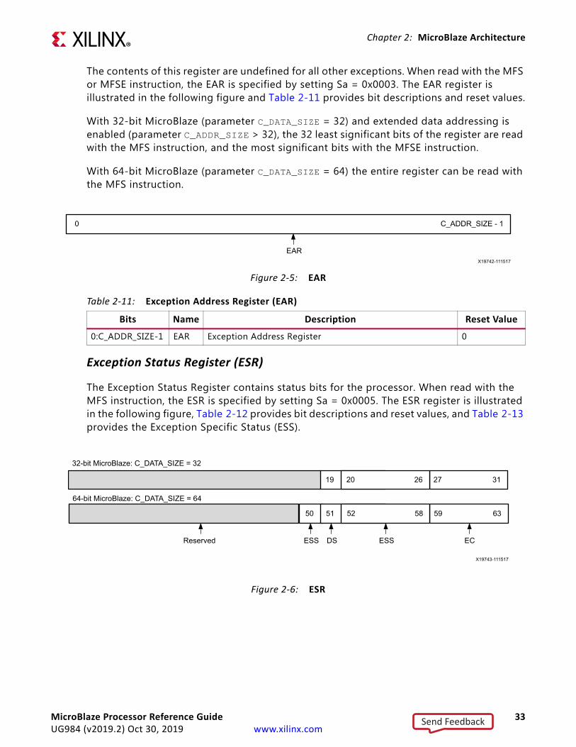
The contents of this register are undefined for all other exceptions. When read with the MFS or MFSE instruction, the EAR is specified by setting Sa = 0x0003. The EAR register is illustrated in the following figure and Table 2-11 provides bit descriptions and reset values.
With 32-bit MicroBlaze (parameter C_DATA_SIZE = 32) and extended data addressing is enabled (parameter C_ADDR_SIZE > 32), the 32 least significant bits of the register are read with the MFS instruction, and the most significant bits with the MFSE instruction.
With 64-bit MicroBlaze (parameter C_DATA_SIZE = 64) the entire register can be read with the MFS instruction.
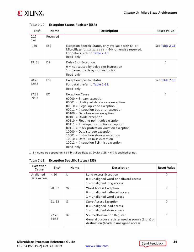
Exception Status Register (ESR)
The Exception Status Register contains status bits for the processor. When read with the MFS instruction, the ESR is specified by setting Sa = 0x0005. The ESR register is illustrated in the following figure, Table 2-12 provides bit descriptions and reset values, and Table 2-13 provides the Exception Specific Status (ESS).
X-Ref Target - Figure 2-5
Figure 2-5: EAR
C_ADDR_SIZE - 1
EAR
0
X19742-111517
Table 2-11: Exception Address Register (EAR)
Bits Name Description Reset Value
0:C_ADDR_SIZE-1 EAR Exception Address Register 0
X-Ref Target - Figure 2-6
Figure 2-6: ESR
63
EC
51
Reserved
595852
ESSDS
3119 272620
32-bit MicroBlaze: C_DATA_SIZE = 32
64-bit MicroBlaze: C_DATA_SIZE = 64
50
ESS
X19743-111517
MicroBlaze Processor Reference Guide 33UG984 (v2019.2) Oct 30, 2019 www.xilinx.com
Send Feedback
Chapter 2: MicroBlaze Architecture
Table 2-12: Exception Status Register (ESR)
Bits1
1. Bit numbers depend on if 64-bit MicroBlaze (C_DATA_SIZE = 64) is enabled or not.
Name Description Reset Value
0:17 0:49
Reserved
-, 50 ESS Exception Specific Status, only available with 64-bit MicroBlaze (C_DATA_SIZE = 64), otherwise reserved. For details refer to Table 2-13. Read-only
See Table 2-13
19, 51 DS Delay Slot Exception.0 = not caused by delay slot instruction 1 = caused by delay slot instructionRead-only
0
20:26 52:58
ESS Exception Specific StatusFor details refer to Table 2-13. Read-only
See Table 2-13
27:31 59:63
EC Exception Cause00000 = Stream exception 00001 = Unaligned data access exception 00010 = Illegal op-code exception 00011 = Instruction bus error exception 00100 = Data bus error exception 00101 = Divide exception 00110 = Floating point unit exception 00111 = Privileged instruction exception 00111 = Stack protection violation exception 10000 = Data storage exception 10001 = Instruction storage exception 10010 = Data TLB miss exception 10011 = Instruction TLB miss exceptionRead-only
0
Table 2-13: Exception Specific Status (ESS) Exception
Cause Bits1 Name Description Reset Value
Unaligned Data Access
-, 50 L Long Access Exception0 = unaligned word or halfword access1 = unaligned long access
0
20, 52 W Word Access Exception0 = unaligned halfword access1 = unaligned word access
0
21, 53 S Store Access Exception0 = unaligned load access1 = unaligned store access
0
22:26 54:58
Rx Source/Destination RegisterGeneral purpose register used as source (Store) or destination (Load) in unaligned access
0
MicroBlaze Processor Reference Guide 34UG984 (v2019.2) Oct 30, 2019 www.xilinx.com
Send Feedback

Chapter 2: MicroBlaze Architecture
Illegal Instruction
20:26 52:58
Reserved 0
Instruction bus error
20, 52 ECC Exception caused by ILMB correctable or uncorrectable error
0
21:26 53:58
Reserved 0
Data bus error
20, 52 ECC Exception caused by DLMB correctable or uncorrectable error
0
21:26 53:58
Reserved 0
Divide 20, 52 DEC Divide - Division exception cause0 = Divide-By-Zero1 = Division Overflow
0
21:26 53:58
Reserved 0
Floating point unit
20:26 52:58
Reserved 0
Privileged instruction
20:26 52:58
Reserved 0
Stack protection violation
20:26 52:58
Reserved 0
Stream 20:22 52:54
Reserved 0
23:26 55:58
FSL AXI4-Stream index that caused the exception 0
Data storage
20, 52 DIZ Data storage - Zone protection0 = Did not occur 1 = Occurred
0
21, 53 S Data storage - Store instruction0 = Did not occur 1 = Occurred
0
22:26 54:58
Reserved 0
Instruction storage
20, 52 DIZ Instruction storage - Zone protection0 = Did not occur 1 = Occurred
0
21:26 53:58
Reserved 0
Table 2-13: Exception Specific Status (ESS) (Cont’d)Exception
Cause Bits1 Name Description Reset Value
MicroBlaze Processor Reference Guide 35UG984 (v2019.2) Oct 30, 2019 www.xilinx.com
Send Feedback

Chapter 2: MicroBlaze Architecture
Branch Target Register (BTR)
The Branch Target Register only exists if the MicroBlaze processor is configured to use exceptions. The register stores the branch target address for all delay slot branch instructions executed while MSR[EIP] = 0. If an exception is caused by an instruction in a delay slot (that is, ESR[DS]=1), the exception handler should return execution to the address stored in BTR instead of the normal exception return address stored in R17. When read with the MFS instruction, the BTR is specified by setting Sa = 0x000B. The BTR register is illustrated in the following figure and Table 2-14 provides bit descriptions and reset values.
When 64-bit MicroBlaze is enabled (C_DATA_SIZE = 64), the Branch Target Register has up to 64 bits, according to the C_ADDR_SIZE parameter, otherwise it has 32 bits.
Floating-Point Status Register (FSR)
The Floating-Point Status Register contains status bits for the floating-point unit. It can be read with an MFS, and written with an MTS instruction. When read or written, the register is specified by setting Sa = 0x0007. The bits in this register are sticky − floating-point
Data TLB miss
20, 52 Reserved 0
21, 53 S Data TLB miss - Store instruction0 = Did not occur 1 = Occurred
0
22:26 54:58
Reserved 0
Instruction TLB miss
20:26 52:58
Reserved 0
1. Bit numbers depend on if 64-bit MicroBlaze (C_DATA_SIZE = 64) is enabled or not.
Table 2-13: Exception Specific Status (ESS) (Cont’d)Exception
Cause Bits1 Name Description Reset Value
X-Ref Target - Figure 2-7
Figure 2-7: BTR
C_ADDR_SIZE - 1
BTR
0
X19744-111517
Table 2-14: Branch Target Register (BTR)
Bits1
1. C_ADDR_SIZE bits with 64-bit MicroBlaze (C_DATA_SIZE = 64) and 32 bits otherwise.
Name Description Reset Value
0:310:C_ADDR_SIZE-1
BTR Branch target address used by handler when returning from an exception caused by an instruction in a delay slot.Read-only
0x0
MicroBlaze Processor Reference Guide 36UG984 (v2019.2) Oct 30, 2019 www.xilinx.com
Send Feedback

Chapter 2: MicroBlaze Architecture
instructions can only set bits in the register, and the only way to clear the register is by using the MTS instruction. The following figure illustrates the FSR register and Table 2-15 provides bit descriptions and reset values.
Exception Data Register (EDR)
The Exception Data Register stores data read on an AXI4-Stream link that caused a stream exception.
The contents of this register are undefined for all other exceptions. When read with the MFS instruction, the EDR is specified by setting Sa = 0x000D. The following figure illustrates the EDR register and Table 2-16 provides bit descriptions and reset values.
Note: The register is only implemented if C_FSL_LINKS is greater than 0 and C_FSL_EXCEPTION is set to 1.
X-Ref Target - Figure 2-8
Figure 2-8: FSR
31302927 280
63
DOReserved
626159
UFOFDZIO
600
32-bit MicroBlaze: C_DATA_SIZE = 32
64-bit MicroBlaze: C_DATA_SIZE = 64
X19745-111517
Table 2-15: Floating Point Status Register (FSR)
Bits1
1. Bit numbers depend on if 64-bit MicroBlaze (C_DATA_SIZE = 64) is enabled or not.
Name Description Reset Value
0:26 0:58
Reserved undefined
27, 59 IO Invalid operation 0
28, 60 DZ Divide-by-zero 0
29, 61 OF Overflow 0
30, 62 UF Underflow 0
31, 63 DO Denormalized operand error 0
X-Ref Target - Figure 2-9
Figure 2-9: EDR
EDR
310
X19746-111517
MicroBlaze Processor Reference Guide 37UG984 (v2019.2) Oct 30, 2019 www.xilinx.com
Send Feedback
Chapter 2: MicroBlaze Architecture
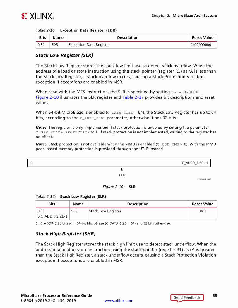
Stack Low Register (SLR)
The Stack Low Register stores the stack low limit use to detect stack overflow. When the address of a load or store instruction using the stack pointer (register R1) as rA is less than the Stack Low Register, a stack overflow occurs, causing a Stack Protection Violation exception if exceptions are enabled in MSR.
When read with the MFS instruction, the SLR is specified by setting Sa = 0x0800. Figure 2-10 illustrates the SLR register and Table 2-17 provides bit descriptions and reset values.
When 64-bit MicroBlaze is enabled (C_DATA_SIZE = 64), the Stack Low Register has up to 64 bits, according to the C_ADDR_SIZE parameter, otherwise it has 32 bits.
Note: The register is only implemented if stack protection is enabled by setting the parameter C_USE_STACK_PROTECTION to 1. If stack protection is not implemented, writing to the register has no effect.
Note: Stack protection is not available when the MMU is enabled (C_USE_MMU > 0). With the MMU page-based memory protection is provided through the UTLB instead.
Stack High Register (SHR)
The Stack High Register stores the stack high limit use to detect stack underflow. When the address of a load or store instruction using the stack pointer (register R1) as rA is greater than the Stack High Register, a stack underflow occurs, causing a Stack Protection Violation exception if exceptions are enabled in MSR.
Table 2-16: Exception Data Register (EDR)
Bits Name Description Reset Value
0:31 EDR Exception Data Register 0x00000000
X-Ref Target - Figure 2-10
Figure 2-10: SLR
SLR
C_ADDR_SIZE - 10
X19747-111517
Table 2-17: Stack Low Register (SLR)
Bits1
1. C_ADDR_SIZE bits with 64-bit MicroBlaze (C_DATA_SIZE = 64) and 32 bits otherwise.
Name Description Reset Value
0:310:C_ADDR_SIZE-1
SLR Stack Low Register 0x0
MicroBlaze Processor Reference Guide 38UG984 (v2019.2) Oct 30, 2019 www.xilinx.com
Send Feedback
Chapter 2: MicroBlaze Architecture
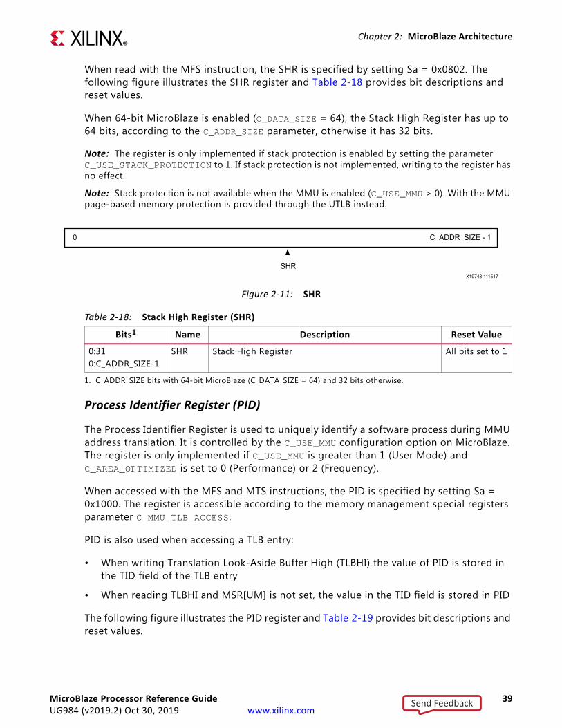
When read with the MFS instruction, the SHR is specified by setting Sa = 0x0802. The following figure illustrates the SHR register and Table 2-18 provides bit descriptions and reset values.
When 64-bit MicroBlaze is enabled (C_DATA_SIZE = 64), the Stack High Register has up to 64 bits, according to the C_ADDR_SIZE parameter, otherwise it has 32 bits.
Note: The register is only implemented if stack protection is enabled by setting the parameter C_USE_STACK_PROTECTION to 1. If stack protection is not implemented, writing to the register has no effect.
Note: Stack protection is not available when the MMU is enabled (C_USE_MMU > 0). With the MMU page-based memory protection is provided through the UTLB instead.
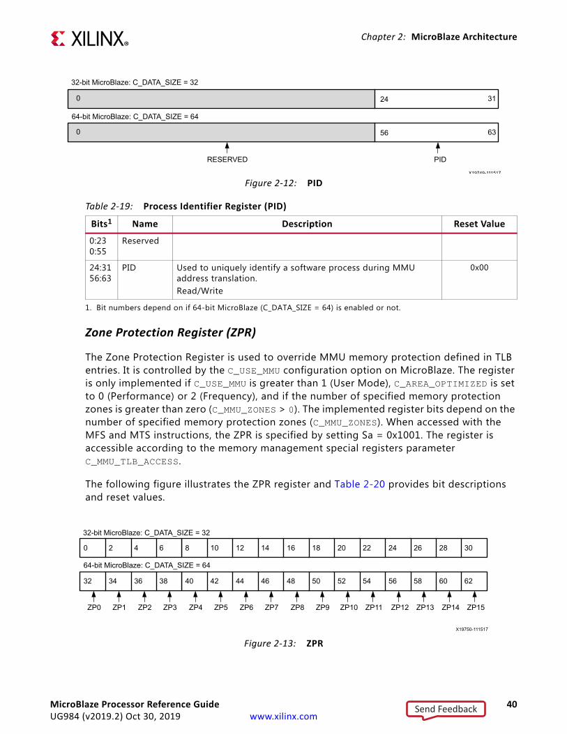
Process Identifier Register (PID)
The Process Identifier Register is used to uniquely identify a software process during MMU address translation. It is controlled by the C_USE_MMU configuration option on MicroBlaze. The register is only implemented if C_USE_MMU is greater than 1 (User Mode) and C_AREA_OPTIMIZED is set to 0 (Performance) or 2 (Frequency).
When accessed with the MFS and MTS instructions, the PID is specified by setting Sa = 0x1000. The register is accessible according to the memory management special registers parameter C_MMU_TLB_ACCESS.
PID is also used when accessing a TLB entry:
• When writing Translation Look-Aside Buffer High (TLBHI) the value of PID is stored in the TID field of the TLB entry
• When reading TLBHI and MSR[UM] is not set, the value in the TID field is stored in PID
The following figure illustrates the PID register and Table 2-19 provides bit descriptions and reset values.
X-Ref Target - Figure 2-11
Figure 2-11: SHR
SHR
C_ADDR_SIZE - 10
X19748-111517
Table 2-18: Stack High Register (SHR)
Bits1
1. C_ADDR_SIZE bits with 64-bit MicroBlaze (C_DATA_SIZE = 64) and 32 bits otherwise.
Name Description Reset Value
0:310:C_ADDR_SIZE-1
SHR Stack High Register All bits set to 1
MicroBlaze Processor Reference Guide 39UG984 (v2019.2) Oct 30, 2019 www.xilinx.com
Send Feedback
Chapter 2: MicroBlaze Architecture
Zone Protection Register (ZPR)
The Zone Protection Register is used to override MMU memory protection defined in TLB entries. It is controlled by the C_USE_MMU configuration option on MicroBlaze. The register is only implemented if C_USE_MMU is greater than 1 (User Mode), C_AREA_OPTIMIZED is set to 0 (Performance) or 2 (Frequency), and if the number of specified memory protection zones is greater than zero (C_MMU_ZONES > 0). The implemented register bits depend on the number of specified memory protection zones (C_MMU_ZONES). When accessed with the MFS and MTS instructions, the ZPR is specified by setting Sa = 0x1001. The register is accessible according to the memory management special registers parameter C_MMU_TLB_ACCESS.
The following figure illustrates the ZPR register and Table 2-20 provides bit descriptions and reset values.
X-Ref Target - Figure 2-12
Figure 2-12: PID
31240
6356
PIDRESERVED
0
32-bit MicroBlaze: C_DATA_SIZE = 32
64-bit MicroBlaze: C_DATA_SIZE = 64
X19749-111517
Table 2-19: Process Identifier Register (PID)
Bits1
1. Bit numbers depend on if 64-bit MicroBlaze (C_DATA_SIZE = 64) is enabled or not.
Name Description Reset Value
0:23 0:55
Reserved
24:31 56:63
PID Used to uniquely identify a software process during MMU address translation.Read/Write
0x00
X-Ref Target - Figure 2-13
Figure 2-13: ZPR
302826242220181614121086420
62
ZP15
60
ZP14
58
ZP13
56
ZP12
54
ZP11
52
ZP10
50
ZP9
48
ZP8
46
ZP7
44
ZP6
42
ZP5
40
ZP4
38
ZP3
36
ZP2
34
ZP1
32
ZP0
32-bit MicroBlaze: C_DATA_SIZE = 32
64-bit MicroBlaze: C_DATA_SIZE = 64
X19750-111517
MicroBlaze Processor Reference Guide 40UG984 (v2019.2) Oct 30, 2019 www.xilinx.com
Send Feedback

Chapter 2: MicroBlaze Architecture
Translation Look-Aside Buffer Low Register (TLBLO)
The Translation Look-Aside Buffer Low Register is used to access MMU Unified Translation Look-Aside Buffer (UTLB) entries. It is controlled by the C_USE_MMU configuration option on MicroBlaze. The register is only implemented if C_USE_MMU is greater than 1 (User Mode), and C_AREA_OPTIMIZED is set to 0 (Performance) or 2 (Frequency). When accessed with the MFS and MTS instructions, the TLBLO is specified by setting Sa = 0x1003.
When reading or writing TLBLO, the UTLB entry indexed by the TLBX register is accessed. The register is readable according to the memory management special registers parameter C_MMU_TLB_ACCESS.
When the MMU Physical Address Extension (PAE) is enabled (parameters C_DATA_SIZE = 32, C_USE_MMU = 3 and C_ADDR_SIZE > 32), the 32 least significant bits of TLBLO are accessed with the MFS and MTS instructions, and the most significant bits with the MFSE and MTSE instruction. When writing the register with PAE enabled, the most significant bits must be written first.
With 64-bit MicroBlaze (parameter C_DATA_SIZE = 64) the entire register can be read with the MFS instruction.
The UTLB is reset on bit stream download (reset value is 0x00000000 for all TLBLO entries).
Note: The UTLB is not reset by the external reset inputs: Reset and Debug_Rst. This means that the entire UTLB must be initialized after reset, to avoid any stale data.
The following figure illustrates the TLBLO register and Table 2-21 provides bit descriptions and reset values. When PAE is enabled the RPN field of the register is extended according
Table 2-20: Zone Protection Register (ZPR)
Bits1
1. Bit numbers depend on if 64-bit MicroBlaze (C_DATA_SIZE = 64) is enabled or not.
Name Description Reset Value
0:12:3...30:31
ZP0ZP1...ZP15
Zone ProtectUser mode (MSR[UM] = 1):00 = Override V in TLB entry. No access to the page is allowed 01 = No override. Use V, WR and EX from TLB entry 10 = No override. Use V, WR and EX from TLB entry 11 = Override WR and EX in TLB entry. Access the page as writable and executablePrivileged mode (MSR[UM] = 0):00 = No override. Use V, WR and EX from TLB entry 01 = No override. Use V, WR and EX from TLB entry 10 = Override WR and EX in TLB entry. Access the page as writable and executable 11 = Override WR and EX in TLB entry. Access the page as writable and executableRead/Write
0x0
32:3334:35...62:63
ZP0ZP1...ZP15
MicroBlaze Processor Reference Guide 41UG984 (v2019.2) Oct 30, 2019 www.xilinx.com
Send Feedback

Chapter 2: MicroBlaze Architecture
to the C_ADDR_SIZE parameter up to 54 bits to be able to hold up to a 64-bit physical address.
X-Ref Target - Figure 2-14
Figure 2-14: TLBLO
0
0
22
n-10 n-9 n-8
28 29 30 31
n-4 n-3 n-2 n-1
32-bit MicroBlaze: (C_ADDR_SIZE = 32 or C_USE_MMU ≠ 3) and (C_DATA_SIZE = 32):
PAE or 64-bit MicroBlaze: (C_ADDR_SIZE > 32 and C_USE_MMU = 3) or (C_DATA_SIZE = 64) (n = C_ADDR_SIZE):
RPN EX WWR ZSEL I M G
23 24
X19751-111517
Table 2-21: Translation Look-Aside Buffer Low Register (TLBLO)
Bits1 Name Description Reset Value
0:21 0:n-11
RPN Real Page Number or Physical Page Number When a TLB hit occurs, this field is read from the TLB entry and is used to form the physical address. Depending on the value of the SIZE field, some of the RPN bits are not used in the physical address. Software must clear unused bits in this field to zero.Only defined when C_USE_MMU=3 (Virtual).Read/Write
0x000000
22 n-10
EX ExecutableWhen bit is set to 1, the page contains executable code, and instructions can be fetched from the page. When bit is cleared to 0, instructions cannot be fetched from the page. Attempts to fetch instructions from a page with a clear EX bit cause an instruction-storage exception.Read/Write
0
23 n-9
WR WritableWhen bit is set to 1, the page is writable and store instructions can be used to store data at addresses within the page. When bit is cleared to 0, the page is read-only (not writable). Attempts to store data into a page with a clear WR bit cause a data storage exception.Read/Write
0
24:27 n-8:n-5
ZSEL Zone SelectThis field selects one of 16 zone fields (Z0-Z15) from the zone-protection register (ZPR). For example, if ZSEL 0x5, zone field Z5 is selected. The selected ZPR field is used to modify the access protection specified by the TLB entry EX and WR fields. It is also used to prevent access to a page by overriding the TLB V (valid) field.Read/Write
0x0
MicroBlaze Processor Reference Guide 42UG984 (v2019.2) Oct 30, 2019 www.xilinx.com
Send Feedback
Chapter 2: MicroBlaze Architecture
Translation Look-Aside Buffer High Register (TLBHI)
The Translation Look-Aside Buffer High Register is used to access MMU Unified Translation Look-Aside Buffer (UTLB) entries. It is controlled by the C_USE_MMU configuration option on MicroBlaze. The register is only implemented if C_USE_MMU is greater than 1 (User Mode), and C_AREA_OPTIMIZED is set to 0 (Performance) or 2 (Frequency). When accessed with the MFS and MTS instructions, the TLBHI is specified by setting Sa = 0x1004. When reading or writing TLBHI, the UTLB entry indexed by the TLBX register is accessed.
The register is readable according to the memory management special registers parameter C_MMU_TLB_ACCESS.
PID is also used when accessing a TLB entry:
• When writing TLBHI the value of PID is stored in the TID field of the TLB entry
• When reading TLBHI and MSR[UM] is not set, the value in the TID field is stored in PID
The UTLB is reset on bit stream download (reset value is 0x00000000 for all TLBHI entries).
28 n-4
W Write ThroughWhen the parameter C_DCACHE_USE_WRITEBACK is set to 1, this bit controls caching policy. A write-through policy is selected when set to 1, and a write-back policy is selected otherwise.This bit is fixed to 1, and write-through is always used, when C_DCACHE_USE_WRITEBACK is cleared to 0.Read/Write
0/1
29 n-3
I Inhibit CachingWhen bit is set to 1, accesses to the page are not cached (caching is inhibited). When cleared to 0, accesses to the page are cacheable.Read/Write
0
30 n-2
M Memory CoherentThis bit is fixed to 0, because memory coherence is not implemented on MicroBlaze.Read Only
0
31 n-1
G GuardedWhen bit is set to 1, speculative page accesses are not allowed (memory is guarded). When cleared to 0, speculative page accesses are allowed. The G attribute can be used to protect memory-mapped I/O devices from inappropriate instruction accesses.Read/Write
0
1. The bit index n = C_ADDR_SIZE applies when PAE or 64-bit MicroBlaze is enabled.
Table 2-21: Translation Look-Aside Buffer Low Register (TLBLO) (Cont’d)
Bits1 Name Description Reset Value
MicroBlaze Processor Reference Guide 43UG984 (v2019.2) Oct 30, 2019 www.xilinx.com
Send Feedback
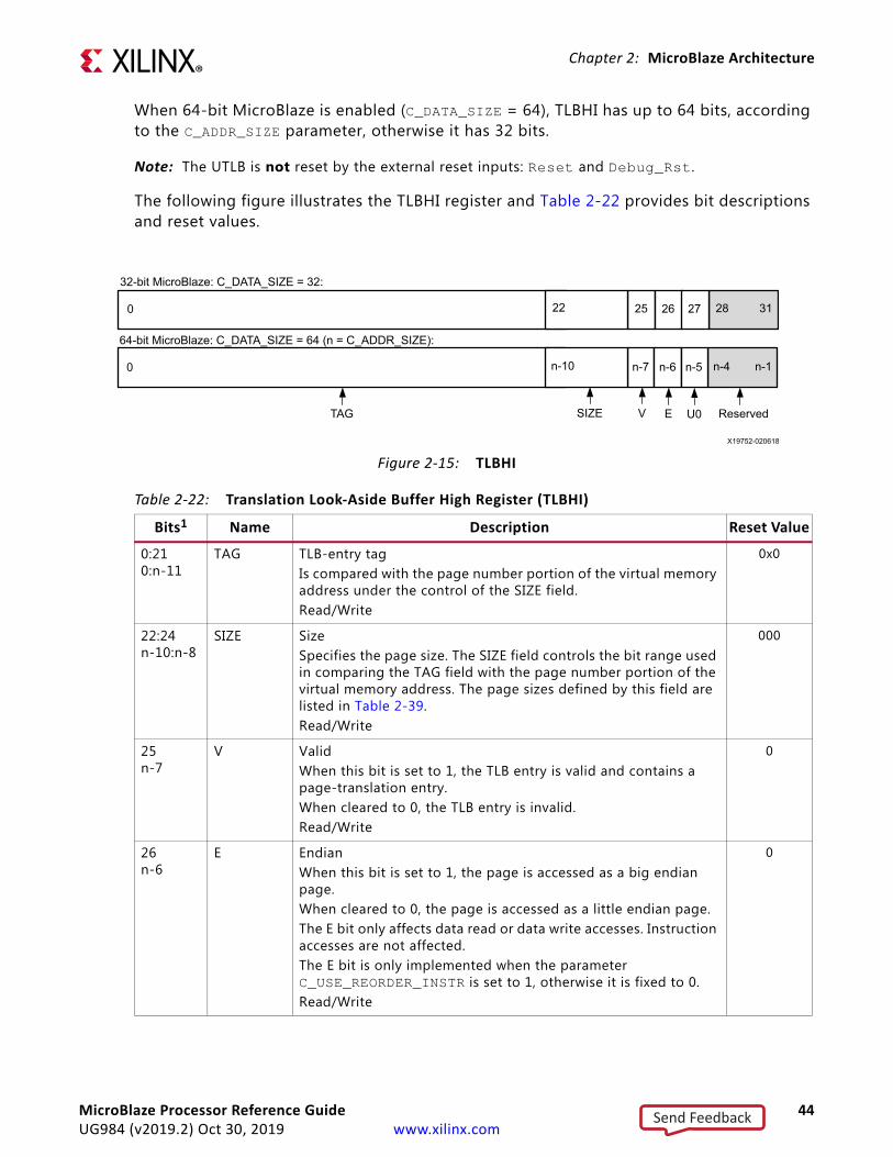
Chapter 2: MicroBlaze Architecture
When 64-bit MicroBlaze is enabled (C_DATA_SIZE = 64), TLBHI has up to 64 bits, according to the C_ADDR_SIZE parameter, otherwise it has 32 bits.
Note: The UTLB is not reset by the external reset inputs: Reset and Debug_Rst.
The following figure illustrates the TLBHI register and Table 2-22 provides bit descriptions and reset values.
X-Ref Target - Figure 2-15
Figure 2-15: TLBHI
TAG
n-100 n-1n-4n-5n-6n-7
SIZE V E U0 Reserved
32-bit MicroBlaze: C_DATA_SIZE = 32:
64-bit MicroBlaze: C_DATA_SIZE = 64 (n = C_ADDR_SIZE):
220 3128272625
X19752-020618
Table 2-22: Translation Look-Aside Buffer High Register (TLBHI)
Bits1 Name Description Reset Value
0:21 0:n-11
TAG TLB-entry tagIs compared with the page number portion of the virtual memory address under the control of the SIZE field.Read/Write
0x0
22:24 n-10:n-8
SIZE SizeSpecifies the page size. The SIZE field controls the bit range used in comparing the TAG field with the page number portion of the virtual memory address. The page sizes defined by this field are listed in Table 2-39.Read/Write
000
25 n-7
V ValidWhen this bit is set to 1, the TLB entry is valid and contains a page-translation entry. When cleared to 0, the TLB entry is invalid.Read/Write
0
26 n-6
E EndianWhen this bit is set to 1, the page is accessed as a big endian page.When cleared to 0, the page is accessed as a little endian page.The E bit only affects data read or data write accesses. Instruction accesses are not affected.The E bit is only implemented when the parameter C_USE_REORDER_INSTR is set to 1, otherwise it is fixed to 0.Read/Write
0
MicroBlaze Processor Reference Guide 44UG984 (v2019.2) Oct 30, 2019 www.xilinx.com
Send Feedback

Chapter 2: MicroBlaze Architecture
Translation Look-Aside Buffer Index Register (TLBX)
The Translation Look-Aside Buffer Index Register is used as an index to the Unified Translation Look-Aside Buffer (UTLB) when accessing the TLBLO and TLBHI registers. It is controlled by the C_USE_MMU configuration option on MicroBlaze. The register is only implemented if C_USE_MMU is greater than 1 (User Mode), and C_AREA_OPTIMIZED is set to 0 (Performance) or 2 (Frequency). When accessed with the MFS and MTS instructions, the TLBX is specified by setting Sa = 0x1002.
The following figure illustrates the TLBX register and Table 2-23 provides bit descriptions and reset values.
27 n-5
U0 User DefinedThis bit is fixed to 0, since there are no user defined storage attributes on MicroBlaze.Read Only
0
28:31 n-4:n-1
Reserved
1. The bit index n = C_ADDR_SIZE applies when 64-bit MicroBlaze is enabled.
Table 2-22: Translation Look-Aside Buffer High Register (TLBHI) (Cont’d) (Cont’d)
Bits1 Name Description Reset Value
X-Ref Target - Figure 2-16
Figure 2-16: TLBX
31260
6358
INDEXReservedMISS
32
32-bit MicroBlaze: C_DATA_SIZE = 32
64-bit MicroBlaze: C_DATA_SIZE = 64
X19753-111517
Table 2-23: Translation Look-Aside Buffer Index Register (TLBX)
Bits1 Name Description Reset Value
0, 32 MISS TLB MissThis bit is cleared to 0 when the TLBSX register is written with a virtual address, and the virtual address is found in a TLB entry. The bit is set to 1 if the virtual address is not found. It is also cleared when the TLBX register itself is written.Read OnlyCan be read if the memory management special registers parameter C_MMU_TLB_ACCESS > 0 (MINIMAL).
0
MicroBlaze Processor Reference Guide 45UG984 (v2019.2) Oct 30, 2019 www.xilinx.com
Send Feedback
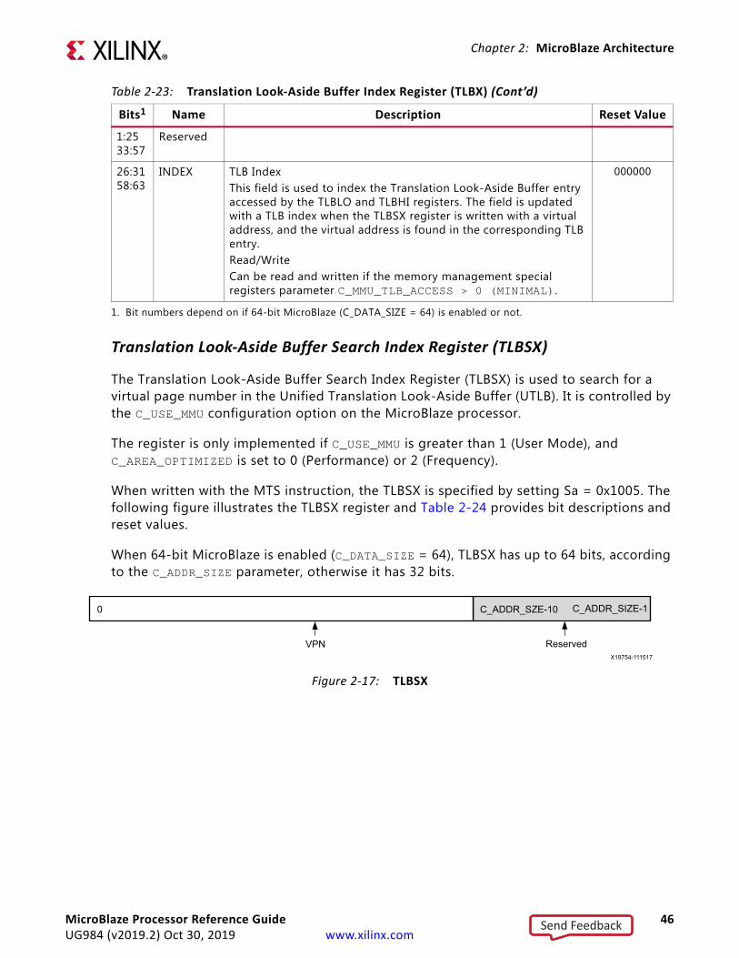
Chapter 2: MicroBlaze Architecture
Translation Look-Aside Buffer Search Index Register (TLBSX)
The Translation Look-Aside Buffer Search Index Register (TLBSX) is used to search for a virtual page number in the Unified Translation Look-Aside Buffer (UTLB). It is controlled by the C_USE_MMU configuration option on the MicroBlaze processor.
The register is only implemented if C_USE_MMU is greater than 1 (User Mode), and C_AREA_OPTIMIZED is set to 0 (Performance) or 2 (Frequency).
When written with the MTS instruction, the TLBSX is specified by setting Sa = 0x1005. The following figure illustrates the TLBSX register and Table 2-24 provides bit descriptions and reset values.
When 64-bit MicroBlaze is enabled (C_DATA_SIZE = 64), TLBSX has up to 64 bits, according to the C_ADDR_SIZE parameter, otherwise it has 32 bits.
1:25 33:57
Reserved
26:31 58:63
INDEX TLB IndexThis field is used to index the Translation Look-Aside Buffer entry accessed by the TLBLO and TLBHI registers. The field is updated with a TLB index when the TLBSX register is written with a virtual address, and the virtual address is found in the corresponding TLB entry.Read/WriteCan be read and written if the memory management special registers parameter C_MMU_TLB_ACCESS > 0 (MINIMAL).
000000
1. Bit numbers depend on if 64-bit MicroBlaze (C_DATA_SIZE = 64) is enabled or not.
Table 2-23: Translation Look-Aside Buffer Index Register (TLBX) (Cont’d)
Bits1 Name Description Reset Value
X-Ref Target - Figure 2-17
Figure 2-17: TLBSX
C_ADDR_SIZE-1C_ADDR_SZE-10
ReservedVPN
0
X19754-111517
MicroBlaze Processor Reference Guide 46UG984 (v2019.2) Oct 30, 2019 www.xilinx.com
Send Feedback

Chapter 2: MicroBlaze Architecture
Processor Version Register (PVR)
The Processor Version Register is controlled by the C_PVR configuration option on MicroBlaze.
• When C_PVR is set to 0 (None) the processor does not implement any PVR and MSR[PVR]=0.
• When C_PVR is set to 1 (Basic), MicroBlaze implements only the first register: PVR0, and if set to 2 (Full), all 13 PVR registers (PVR0 to PVR12) are implemented.
When read with the MFS or MFSE instruction the PVR is specified by setting Sa = 0x200x, with x being the register number between 0x0 and 0xB.
With extended data addressing is enabled (parameter C_DATA_SIZE = 32 and C_ADDR_SIZE > 32), the 32 least significant bits of PVR8 and PVR9 are read with the MFS instruction, and the most significant bits with the MFSE instruction.
When physical address extension (PAE) is enabled (parameters C_DATA_SIZE = 32, C_USE_MMU = 3 and C_ADDR_SIZE > 32), the 32 least significant bits of PVR6 and PVR7 are read with the MFS instruction, and the most significant bits with the MFSE instruction.
With 64-bit MicroBlaze (parameter C_DATA_SIZE = 64) the entire contents of the PVR6 - PVR9 and PVR12 registers can be read with the MFS instruction.
Table 2-25 through Table 2-37 provide bit descriptions and values.
Table 2-24: Translation Look-Aside Buffer Index Search Register (TLBSX)
Bits1
1. The bit index n = C_ADDR_SIZE applies when 64-bit MicroBlaze is enabled.
Name Description Reset Value
0:21 0:n-9
VPN Virtual Page NumberThis field represents the page number portion of the virtual memory address. It is compared with the page number portion of the virtual memory address under the control of the SIZE field, in each of the Translation Look-Aside Buffer entries that have the V bit set to 1.If the virtual page number is found, the TLBX register is written with the index of the TLB entry and the MISS bit in TLBX is cleared to 0. If the virtual page number is not found in any of the TLB entries, the MISS bit in the TLBX register is set to 1.Write Only
22:31 n-10:n-1
Reserved
MicroBlaze Processor Reference Guide 47UG984 (v2019.2) Oct 30, 2019 www.xilinx.com
Send Feedback
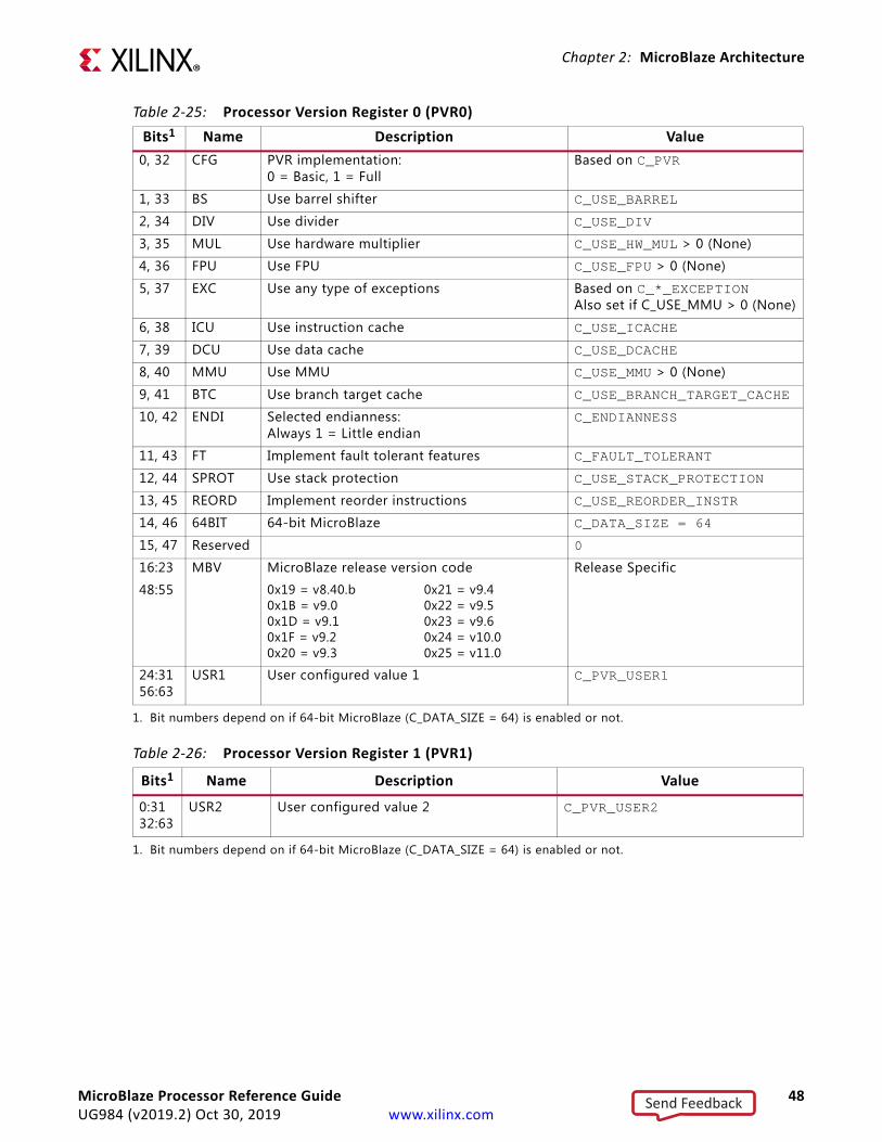
Chapter 2: MicroBlaze Architecture
Table 2-25: Processor Version Register 0 (PVR0) Bits1
1. Bit numbers depend on if 64-bit MicroBlaze (C_DATA_SIZE = 64) is enabled or not.
Name Description Value0, 32 CFG PVR implementation:
0 = Basic, 1 = FullBased on C_PVR
1, 33 BS Use barrel shifter C_USE_BARREL
2, 34 DIV Use divider C_USE_DIV
3, 35 MUL Use hardware multiplier C_USE_HW_MUL > 0 (None)
4, 36 FPU Use FPU C_USE_FPU > 0 (None)
5, 37 EXC Use any type of exceptions Based on C_*_EXCEPTION Also set if C_USE_MMU > 0 (None)
6, 38 ICU Use instruction cache C_USE_ICACHE
7, 39 DCU Use data cache C_USE_DCACHE
8, 40 MMU Use MMU C_USE_MMU > 0 (None)
9, 41 BTC Use branch target cache C_USE_BRANCH_TARGET_CACHE
10, 42 ENDI Selected endianness: Always 1 = Little endian
C_ENDIANNESS
11, 43 FT Implement fault tolerant features C_FAULT_TOLERANT
12, 44 SPROT Use stack protection C_USE_STACK_PROTECTION
13, 45 REORD Implement reorder instructions C_USE_REORDER_INSTR
14, 46 64BIT 64-bit MicroBlaze C_DATA_SIZE = 64
15, 47 Reserved 0
16:23 MBV MicroBlaze release version code Release Specific
48:55 0x19 = v8.40.b 0x1B = v9.0 0x1D = v9.1 0x1F = v9.2 0x20 = v9.3
0x21 = v9.4 0x22 = v9.5 0x23 = v9.6 0x24 = v10.0 0x25 = v11.0
24:31 56:63
USR1 User configured value 1 C_PVR_USER1
Table 2-26: Processor Version Register 1 (PVR1)
Bits1
1. Bit numbers depend on if 64-bit MicroBlaze (C_DATA_SIZE = 64) is enabled or not.
Name Description Value
0:31 32:63
USR2 User configured value 2 C_PVR_USER2
MicroBlaze Processor Reference Guide 48UG984 (v2019.2) Oct 30, 2019 www.xilinx.com
Send Feedback

Chapter 2: MicroBlaze Architecture
Table 2-27: Processor Version Register 2 (PVR2)
Bits1 Name Description Value
0, 32 DAXI Data side AXI4 or ACE in use C_D_AXI
1, 33 DLMB Data side LMB in use C_D_LMB
2, 34 IAXI Instruction side AXI4 or ACE in use C_I_AXI
3, 35 ILMB Instruction side LMB in use C_I_LMB
4, 36 IRQEDGE Interrupt is edge triggered C_INTERRUPT_IS_EDGE
5, 37 IRQPOS Interrupt edge is positive C_EDGE_IS_POSITIVE
6, 38 CEEXC Generate bus exceptions for ECC correctable errors in LMB memory
C_ECC_USE_CE_EXCEPTION
7, 39 FREQ Select implementation to optimize processor frequency
C_AREA_OPTIMIZED=2 (Frequency)
8, 40 Reserved 0
9, 41 Reserved 1
10, 42 ACE Use ACE interconnect C_INTERCONNECT = 3 (ACE)
11, 43 AXI4DP Data Peripheral AXI interface uses AXI4 protocol, with support for exclusive access
C_M_AXI_DP_EXCLUSIVE_ACCESS
12, 44 FSL Use extended AXI4-Stream instructions C_USE_EXTENDED_FSL_INSTR
13, 45 FSLEXC Generate exception for AXI4-Stream control bit mismatch
C_FSL_EXCEPTION
14, 46 MSR Use msrset and msrclr instructions C_USE_MSR_INSTR
15, 47 PCMP Use pattern compare and CLZ instructions C_USE_PCMP_INSTR
16, 48 AREA Select implementation to optimize area with lower instruction throughput
C_AREA_OPTIMIZED = 1 (Area)
17, 49 BS Use barrel shifter C_USE_BARREL
18, 50 DIV Use divider C_USE_DIV
19, 51 MUL Use hardware multiplier C_USE_HW_MUL > 0 (None)
20, 52 FPU Use FPU C_USE_FPU > 0 (None)
21, 53 MUL64 Use 64-bit hardware multiplier C_USE_HW_MUL = 2 (Mul64)
22, 54 FPU2 Use floating point conversion and square root instructions
C_USE_FPU = 2 (Extended)
23, 55 IMPEXC Allow imprecise exceptions for ECC errors in LMB memory
C_IMPRECISE_EXCEPTIONS
24, 56 Reserved 0
25, 57 OP0EXC Generate exception for 0x0 illegal opcode C_OPCODE_0x0_ILLEGAL
26, 58 UNEXC Generate exception for unaligned data access
C_UNALIGNED_EXCEPTIONS
27, 59 OPEXC Generate exception for any illegal opcode C_ILL_OPCODE_EXCEPTION
28, 60 AXIDEXC Generate exception for M_AXI_D error C_M_AXI_D_BUS_EXCEPTION
MicroBlaze Processor Reference Guide 49UG984 (v2019.2) Oct 30, 2019 www.xilinx.com
Send Feedback
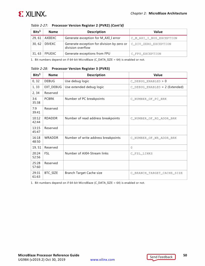
Chapter 2: MicroBlaze Architecture
29, 61 AXIIEXC Generate exception for M_AXI_I error C_M_AXI_I_BUS_EXCEPTION
30, 62 DIVEXC Generate exception for division by zero or division overflow
C_DIV_ZERO_EXCEPTION
31, 63 FPUEXC Generate exceptions from FPU C_FPU_EXCEPTION
1. Bit numbers depend on if 64-bit MicroBlaze (C_DATA_SIZE = 64) is enabled or not.
Table 2-28: Processor Version Register 3 (PVR3)
Bits1
1. Bit numbers depend on if 64-bit MicroBlaze (C_DATA_SIZE = 64) is enabled or not.
Name Description Value
0, 32 DEBUG Use debug logic C_DEBUG_ENABLED > 0
1, 33 EXT_DEBUG Use extended debug logic C_DEBUG_ENABLED = 2 (Extended)
2, 34 Reserved
3:6 35:38
PCBRK Number of PC breakpoints C_NUMBER_OF_PC_BRK
7:9 39:41
Reserved
10:12 42:44
RDADDR Number of read address breakpoints C_NUMBER_OF_RD_ADDR_BRK
13:15 45:47
Reserved
16:18 48:50
WRADDR Number of write address breakpoints C_NUMBER_OF_WR_ADDR_BRK
19, 51 Reserved 0
20:24 52:56
FSL Number of AXI4-Stream links C_FSL_LINKS
25:28 57:60
Reserved
29:31 61:63
BTC_SIZE Branch Target Cache size C_BRANCH_TARGET_CACHE_SIZE
Table 2-27: Processor Version Register 2 (PVR2) (Cont’d)
Bits1 Name Description Value
MicroBlaze Processor Reference Guide 50UG984 (v2019.2) Oct 30, 2019 www.xilinx.com
Send Feedback
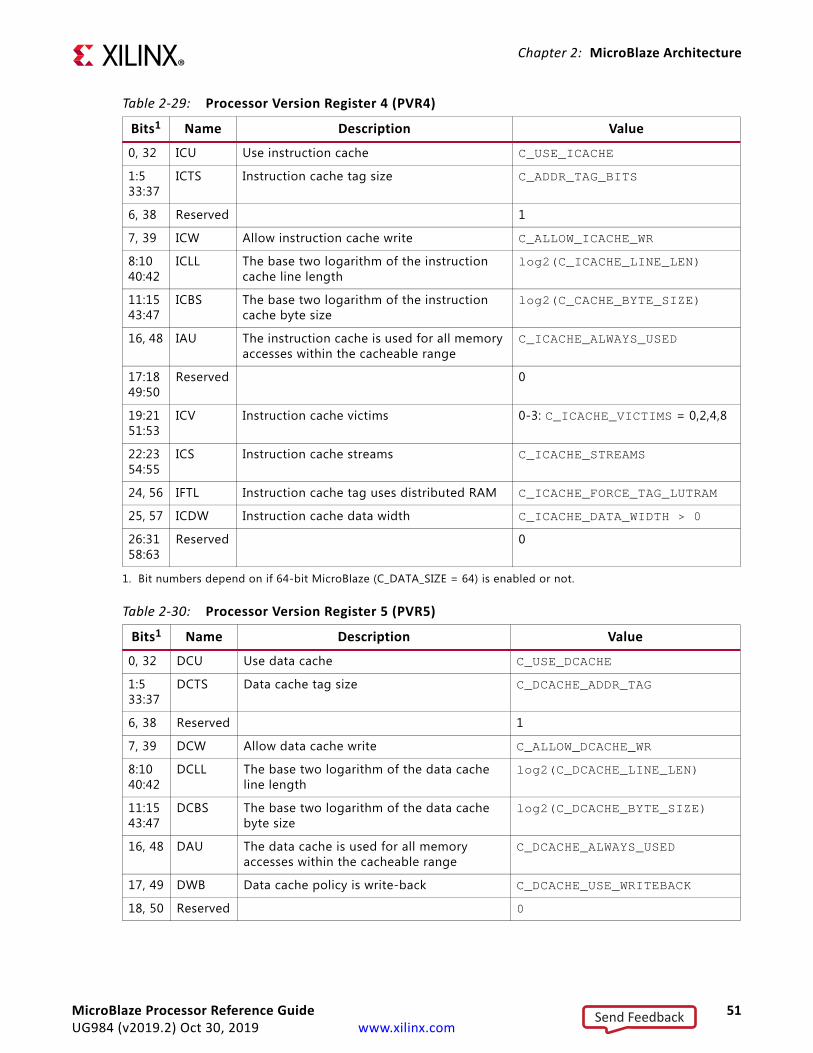
Chapter 2: MicroBlaze Architecture
Table 2-29: Processor Version Register 4 (PVR4)
Bits1
1. Bit numbers depend on if 64-bit MicroBlaze (C_DATA_SIZE = 64) is enabled or not.
Name Description Value
0, 32 ICU Use instruction cache C_USE_ICACHE
1:5 33:37
ICTS Instruction cache tag size C_ADDR_TAG_BITS
6, 38 Reserved 1
7, 39 ICW Allow instruction cache write C_ALLOW_ICACHE_WR
8:10 40:42
ICLL The base two logarithm of the instruction cache line length
log2(C_ICACHE_LINE_LEN)
11:15 43:47
ICBS The base two logarithm of the instruction cache byte size
log2(C_CACHE_BYTE_SIZE)
16, 48 IAU The instruction cache is used for all memory accesses within the cacheable range
C_ICACHE_ALWAYS_USED
17:18 49:50
Reserved 0
19:21 51:53
ICV Instruction cache victims 0-3: C_ICACHE_VICTIMS = 0,2,4,8
22:23 54:55
ICS Instruction cache streams C_ICACHE_STREAMS
24, 56 IFTL Instruction cache tag uses distributed RAM C_ICACHE_FORCE_TAG_LUTRAM
25, 57 ICDW Instruction cache data width C_ICACHE_DATA_WIDTH > 0
26:31 58:63
Reserved 0
Table 2-30: Processor Version Register 5 (PVR5)
Bits1 Name Description Value
0, 32 DCU Use data cache C_USE_DCACHE
1:5 33:37
DCTS Data cache tag size C_DCACHE_ADDR_TAG
6, 38 Reserved 1
7, 39 DCW Allow data cache write C_ALLOW_DCACHE_WR
8:10 40:42
DCLL The base two logarithm of the data cache line length
log2(C_DCACHE_LINE_LEN)
11:15 43:47
DCBS The base two logarithm of the data cache byte size
log2(C_DCACHE_BYTE_SIZE)
16, 48 DAU The data cache is used for all memory accesses within the cacheable range
C_DCACHE_ALWAYS_USED
17, 49 DWB Data cache policy is write-back C_DCACHE_USE_WRITEBACK
18, 50 Reserved 0
MicroBlaze Processor Reference Guide 51UG984 (v2019.2) Oct 30, 2019 www.xilinx.com
Send Feedback

Chapter 2: MicroBlaze Architecture
19:21 51:53
DCV Data cache victims 0-3: C_DCACHE_VICTIMS = 0,2,4,8
22:23 54:55
Reserved 0
24, 56 DFTL Data cache tag uses distributed RAM C_DCACHE_FORCE_TAG_LUTRAM
25, 57 DCDW Data cache data width C_DCACHE_DATA_WIDTH > 0
26, 58 AXI4DC Data Cache AXI interface uses AXI4 protocol, with support for exclusive access
C_M_AXI_DC_EXCLUSIVE_ACCESS
27:31 59:63
Reserved 0
1. Bit numbers depend on if 64-bit MicroBlaze (C_DATA_SIZE = 64) is enabled or not.
Table 2-31: Processor Version Register 6 (PVR6)
Bits Name Description Value
0:C_ADDR_SIZE-1 ICBA Instruction Cache Base Address C_ICACHE_BASEADDR
Table 2-32: Processor Version Register 7 (PVR7)
Bits Name Description Value
0:C_ADDR_SIZE-1 ICHA Instruction Cache High Address C_ICACHE_HIGHADDR
Table 2-33: Processor Version Register 8 (PVR8)
Bits Name Description Value
0:C_ADDR_SIZE-1 DCBA Data Cache Base Address C_DCACHE_BASEADDR
Table 2-34: Processor Version Register 9 (PVR9)
Bits Name Description Value
0:C_ADDR_SIZE-1 DCHA Data Cache High Address C_DCACHE_HIGHADDR
Table 2-30: Processor Version Register 5 (PVR5) (Cont’d)
Bits1 Name Description Value
MicroBlaze Processor Reference Guide 52UG984 (v2019.2) Oct 30, 2019 www.xilinx.com
Send Feedback

Chapter 2: MicroBlaze Architecture
Table 2-35: Processor Version Register 10 (PVR10)
Bits1
1. Bit numbers depend on if 64-bit MicroBlaze (C_DATA_SIZE = 64) is enabled or not.
Name Description Value
0:7 ARCH Target architecture: Defined by parameter C_FAMILY
32:39 0xF0x100x11 0x12
0x130x140x150x160x17 0x18
===
=
===== =
Virtex®-7, Defense Grade Virtex-7 QKintex®-7, Defense Grade Kintex-7 QArtix®-7, Automotive Artix-7, Defense Grade Artix-7 QZynq®-7000, Automotive Zynq-7000, Defense Grade Zynq-7000 QUltraScale™ VirtexUltraScale KintexUltraScale+™ ZynqUltraScale+ VirtexUltraScale+ Kintex Spartan®-7
8:13 40:45
ASIZE Number of extended address bits C_ADDR_SIZE - 32
14:31 46:63
Reserved 0
Table 2-36: Processor Version Register 11 (PVR11) Bits1
1. Bit numbers depend on if 64-bit MicroBlaze (C_DATA_SIZE = 64) is enabled or not.
Name Description Value0:1 32:33
MMU Use MMU: C_USE_MMU
0 = None 1 = User Mode
2 = Protection 3 = Virtual
2:4 34:36
ITLB Instruction Shadow TLB size log2(C_MMU_ITLB_SIZE)
5:7 37:39
DTLB Data Shadow TLB size log2(C_MMU_DTLB_SIZE)
8:9 40:41
TLBACC TLB register access: C_MMU_TLB_ACCESS
0 = Minimal 1 = Read
2 = Write 3 = Full
10:14 42:46
ZONES Number of memory protection zones C_MMU_ZONES
15, 47 PRIVINS Privileged instructions:0 = Full protection 1 = Allow stream instructions
C_MMU_PRIVILEGED_INSTR
16, 48 Reserved Reserved for future use 0
17:31 49:63
RSTMSR Reset value for MSR C_RESET_MSR_IE << 2 | C_RESET_MSR_BIP << 4 | C_RESET_MSR_ICE << 6 | C_RESET_MSR_DCE << 8 | C_RESET_MSR_EE << 9 | C_RESET_MSR_EIP << 10
MicroBlaze Processor Reference Guide 53UG984 (v2019.2) Oct 30, 2019 www.xilinx.com
Send Feedback

Chapter 2: MicroBlaze Architecture
Table 2-37: Processor Version Register 12 (PVR12)
Bits1
1. C_ADDR_SIZE bits with 64-bit MicroBlaze (C_DATA_SIZE = 64) and 32 bits otherwise.
Name Description Value0:31 0:C_ADDR_SIZE-1
VECTORS Location of MicroBlaze vectors C_BASE_VECTORS
MicroBlaze Processor Reference Guide 54UG984 (v2019.2) Oct 30, 2019 www.xilinx.com
Send Feedback

Chapter 2: MicroBlaze Architecture
Pipeline ArchitectureMicroBlaze instruction execution is pipelined. For most instructions, each stage takes one clock cycle to complete. Consequently, the number of clock cycles necessary for a specific instruction to complete is equal to the number of pipeline stages, and one instruction is completed on every cycle in the absence of data, control or structural hazards.
A data hazard occurs when the result of an instruction is needed by a subsequent instruction. This can result in stalling the pipeline, unless the result can be forwarded to the subsequent instruction. The MicroBlaze GNU Compiler attempts to avoid data hazards by reordering instructions during optimization.
A control hazard occurs when a branch is taken, and the next instruction is not immediately available. This results in stalling the pipeline. MicroBlaze provides delay slot branches and the optional branch target cache to reduce the number of stall cycles.
A structural hazard occurs for a few instructions that require multiple clock cycles in the execute stage or a later stage to complete. This is achieved by stalling the pipeline.
Load and store instructions accessing slower memory might take multiple cycles. The pipeline is stalled until the access completes. MicroBlaze provides the optional data cache to improve the average latency of slower memory.
When executing from slower memory, instruction fetches might take multiple cycles. This additional latency directly affects the efficiency of the pipeline. MicroBlaze implements an instruction prefetch buffer that reduces the impact of such multi-cycle instruction memory latency. While the pipeline is stalled for any other reason, the prefetch buffer continues to load sequential instructions speculatively. When the pipeline resumes execution, the fetch stage can load new instructions directly from the prefetch buffer instead of waiting for the instruction memory access to complete.
If instructions are modified during execution (for example with self-modifying code), the prefetch buffer should be emptied before executing the modified instructions, to ensure that it does not contain the old unmodified instructions.
RECOMMENDED: The recommended way to do this is using an MBAR instruction, although it is also possible to use a synchronizing branch instruction, for example BRI 4.
MicroBlaze also provides the optional instruction cache to improve the average instruction fetch latency of slower memory.
All hazards are independent, and can potentially occur simultaneously. In such cases, the number of cycles the pipeline is stalled is defined by the hazard with the longest stall duration.
MicroBlaze Processor Reference Guide 55UG984 (v2019.2) Oct 30, 2019 www.xilinx.com
Send Feedback
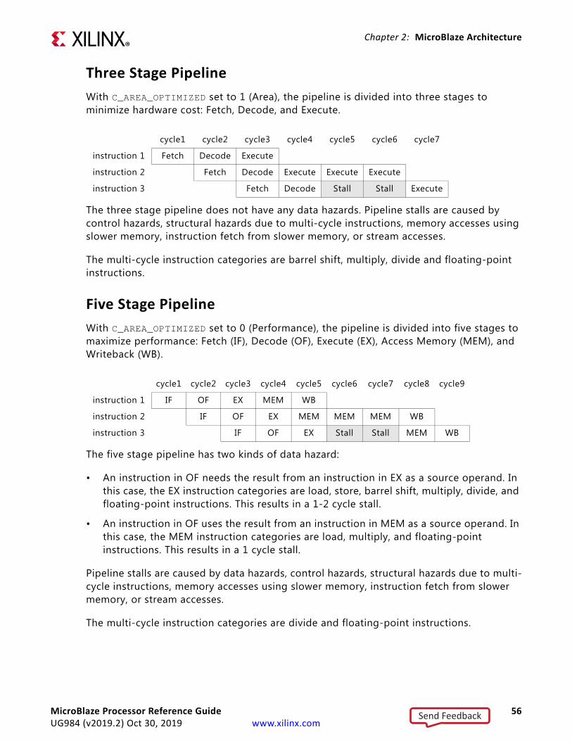
Chapter 2: MicroBlaze Architecture
Three Stage PipelineWith C_AREA_OPTIMIZED set to 1 (Area), the pipeline is divided into three stages to minimize hardware cost: Fetch, Decode, and Execute.
The three stage pipeline does not have any data hazards. Pipeline stalls are caused by control hazards, structural hazards due to multi-cycle instructions, memory accesses using slower memory, instruction fetch from slower memory, or stream accesses.
The multi-cycle instruction categories are barrel shift, multiply, divide and floating-point instructions.
Five Stage PipelineWith C_AREA_OPTIMIZED set to 0 (Performance), the pipeline is divided into five stages to maximize performance: Fetch (IF), Decode (OF), Execute (EX), Access Memory (MEM), and Writeback (WB).
The five stage pipeline has two kinds of data hazard:
• An instruction in OF needs the result from an instruction in EX as a source operand. In this case, the EX instruction categories are load, store, barrel shift, multiply, divide, and floating-point instructions. This results in a 1-2 cycle stall.
• An instruction in OF uses the result from an instruction in MEM as a source operand. In this case, the MEM instruction categories are load, multiply, and floating-point instructions. This results in a 1 cycle stall.
Pipeline stalls are caused by data hazards, control hazards, structural hazards due to multi-cycle instructions, memory accesses using slower memory, instruction fetch from slower memory, or stream accesses.
The multi-cycle instruction categories are divide and floating-point instructions.
cycle1 cycle2 cycle3 cycle4 cycle5 cycle6 cycle7
instruction 1 Fetch Decode Execute
instruction 2 Fetch Decode Execute Execute Execute
instruction 3 Fetch Decode Stall Stall Execute
cycle1 cycle2 cycle3 cycle4 cycle5 cycle6 cycle7 cycle8 cycle9
instruction 1 IF OF EX MEM WB
instruction 2 IF OF EX MEM MEM MEM WB
instruction 3 IF OF EX Stall Stall MEM WB
MicroBlaze Processor Reference Guide 56UG984 (v2019.2) Oct 30, 2019 www.xilinx.com
Send Feedback
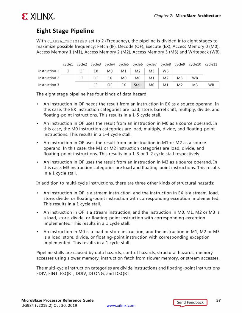
Chapter 2: MicroBlaze Architecture
Eight Stage PipelineWith C_AREA_OPTIMIZED set to 2 (Frequency), the pipeline is divided into eight stages to maximize possible frequency: Fetch (IF), Decode (OF), Execute (EX), Access Memory 0 (M0), Access Memory 1 (M1), Access Memory 2 (M2), Access Memory 3 (M3) and Writeback (WB).
The eight stage pipeline has four kinds of data hazard:
• An instruction in OF needs the result from an instruction in EX as a source operand. In this case, the EX instruction categories are load, store, barrel shift, multiply, divide, and floating-point instructions. This results in a 1-5 cycle stall.
• An instruction in OF uses the result from an instruction in M0 as a source operand. In this case, the M0 instruction categories are load, multiply, divide, and floating-point instructions. This results in a 1-4 cycle stall.
• An instruction in OF uses the result from an instruction in M1 or M2 as a source operand. In this case, the M1 or M2 instruction categories are load, divide, and floating-point instructions. This results in a 1-3 or 1-2 cycle stall respectively.
• An instruction in OF uses the result from an instruction in M3 as a source operand. In this case, M3 instruction categories are load and floating-point instructions. This results in a 1 cycle stall.
In addition to multi-cycle instructions, there are three other kinds of structural hazards:
• An instruction in OF is a stream instruction, and the instruction in EX is a stream, load, store, divide, or floating-point instruction with corresponding exception implemented. This results in a 1 cycle stall.
• An instruction in OF is a stream instruction, and the instruction in M0, M1, M2 or M3 is a load, store, divide, or floating-point instruction with corresponding exception implemented. This results in a 1 cycle stall.
• An instruction in M0 is a load or store instruction, and the instruction in M1, M2 or M3 is a load, store, divide, or floating-point instruction with corresponding exception implemented. This results in a 1 cycle stall.
Pipeline stalls are caused by data hazards, control hazards, structural hazards, memory accesses using slower memory, instruction fetch from slower memory, or stream accesses.
The multi-cycle instruction categories are divide instructions and floating-point instructions FDIV, FINT, FSQRT, DDIV, DLONG, and DSQRT.
cycle1 cycle2 cycle3 cycle4 cycle5 cycle6 cycle7 cycle8 cycle9 cycle10 cycle11
instruction 1 IF OF EX M0 M1 M2 M3 WB
instruction 2 IF OF EX M0 M0 M1 M2 M3 WB
instruction 3 IF OF EX Stall M0 M1 M2 M3 WB
MicroBlaze Processor Reference Guide 57UG984 (v2019.2) Oct 30, 2019 www.xilinx.com
Send Feedback
Chapter 2: MicroBlaze Architecture
BranchesNormally the instructions in the fetch and decode stages (as well as prefetch buffer) are flushed when executing a taken branch. The fetch pipeline stage is then reloaded with a new instruction from the calculated branch address. A taken branch in MicroBlaze takes three clock cycles to execute, two of which are required for refilling the pipeline. To reduce this latency overhead, MicroBlaze supports branches with delay slots and the optional branch target cache.
Delay Slots
When executing a taken branch with delay slot, only the fetch pipeline stage in MicroBlaze is flushed. The instruction in the decode stage (branch delay slot) is allowed to complete. This technique effectively reduces the branch penalty from two clock cycles to one. Branch instructions with delay slots have a D appended to the instruction mnemonic. For example, the BNE instruction does not execute the subsequent instruction (does not have a delay slot), whereas BNED executes the next instruction before control is transferred to the branch location.
A delay slot must not contain the following instructions: IMM, IMML, branch, or break. Interrupts and external hardware breaks are deferred until after the delay slot branch has been completed. Instructions that could cause recoverable exceptions (for example unaligned word or halfword load and store) are allowed in the delay slot.
If an exception is caused in a delay slot the ESR[DS] bit is set, and the exception handler is responsible for returning the execution to the branch target (stored in the special purpose register BTR). If the ESR[DS] bit is set, register R17 is not valid (otherwise it contains the address following the instruction causing the exception).
Branch Target Cache
To improve branch performance, MicroBlaze provides a branch target cache (BTC) coupled with a branch prediction scheme. With the BTC enabled, a correctly predicted immediate branch or return instruction incurs no overhead.
The BTC operates by saving the target address of each immediate branch and return instruction the first time the instruction is encountered. The next time it is encountered, it is usually found in the Branch Target Cache, and the Instruction Fetch Program Counter is then simply changed to the saved target address, in case the branch should be taken. Unconditional branches and return instructions are always taken, whereas conditional branches use branch prediction, to avoid taking a branch that should not have been taken and vice versa.
The BTC is cleared when a memory barrier (MBAR 0) or synchronizing branch (BRI 4) is executed. This also occurs when the memory barrier or synchronizing branch follows immediately after a branch instruction, even if that branch is taken. To avoid inadvertently
MicroBlaze Processor Reference Guide 58UG984 (v2019.2) Oct 30, 2019 www.xilinx.com
Send Feedback
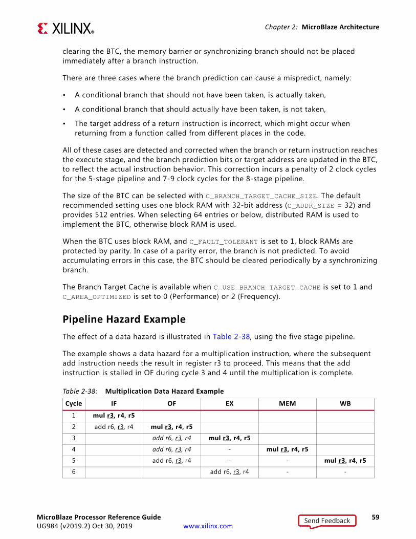
Chapter 2: MicroBlaze Architecture
clearing the BTC, the memory barrier or synchronizing branch should not be placed immediately after a branch instruction.
There are three cases where the branch prediction can cause a mispredict, namely:
• A conditional branch that should not have been taken, is actually taken,
• A conditional branch that should actually have been taken, is not taken,
• The target address of a return instruction is incorrect, which might occur when returning from a function called from different places in the code.
All of these cases are detected and corrected when the branch or return instruction reaches the execute stage, and the branch prediction bits or target address are updated in the BTC, to reflect the actual instruction behavior. This correction incurs a penalty of 2 clock cycles for the 5-stage pipeline and 7-9 clock cycles for the 8-stage pipeline.
The size of the BTC can be selected with C_BRANCH_TARGET_CACHE_SIZE. The default recommended setting uses one block RAM with 32-bit address (C_ADDR_SIZE = 32) and provides 512 entries. When selecting 64 entries or below, distributed RAM is used to implement the BTC, otherwise block RAM is used.
When the BTC uses block RAM, and C_FAULT_TOLERANT is set to 1, block RAMs are protected by parity. In case of a parity error, the branch is not predicted. To avoid accumulating errors in this case, the BTC should be cleared periodically by a synchronizing branch.
The Branch Target Cache is available when C_USE_BRANCH_TARGET_CACHE is set to 1 and C_AREA_OPTIMIZED is set to 0 (Performance) or 2 (Frequency).
Pipeline Hazard ExampleThe effect of a data hazard is illustrated in Table 2-38, using the five stage pipeline.
The example shows a data hazard for a multiplication instruction, where the subsequent add instruction needs the result in register r3 to proceed. This means that the add instruction is stalled in OF during cycle 3 and 4 until the multiplication is complete.
Table 2-38: Multiplication Data Hazard Example
Cycle IF OF EX MEM WB1 mul r3, r4, r5
2 add r6, r3, r4 mul r3, r4, r5
3 add r6, r3, r4 mul r3, r4, r5
4 add r6, r3, r4 - mul r3, r4, r5
5 add r6, r3, r4 - - mul r3, r4, r5
6 add r6, r3, r4 - -
MicroBlaze Processor Reference Guide 59UG984 (v2019.2) Oct 30, 2019 www.xilinx.com
Send Feedback
Chapter 2: MicroBlaze Architecture
Avoiding Data HazardsIn some cases, the MicroBlaze GNU Compiler is not able to optimize code to completely avoid data hazards. However, it is often possible to change the source code in order to achieve this, mainly by better utilization of the general purpose registers.
Two C code examples are shown here:
• Multiplication of a static array in memory
static int a[4], b[4], c[4];register int a0, a1, a2, a3, b0, b1, b2, b3, c0, c1, c2, c3;
a0 = a[0]; a1 = a[1]; a2 = a[2]; a3 = a[3];b0 = b[0]; b1 = b[1]; b2 = b[2]; b3 = b[3];c0 = a0 * b0; c1 = a1 * b1; c2 = a2 * b2; c3 = a3 * b3;c[3] = c3; c2 = c[2]; c1 = c[1]; c0 = c[0];
This code ensures that load instructions are first executed to load operands into separate registers, which are then multiplied and finally stored. The code can be extended up to 8 multiplications without running out of general purpose registers.
• Fetching a data packet from an AXI4-Stream interface.
#include <mb_interface.h>
static int a[4];register int a0, a1, a2, a3;
getfsl(a0, 0); getfsl(a1, 0); getfsl(a2, 0); getfsl(a3, 0);a[3] = a3; a[1] = a1; a[2] = a2; a[0] = a0;
This code ensures that get instructions using different registers are first executed, and then data is stored. The code can be extended to up to 16 accesses without running out of general purpose registers.
MicroBlaze Processor Reference Guide 60UG984 (v2019.2) Oct 30, 2019 www.xilinx.com
Send Feedback

Chapter 2: MicroBlaze Architecture
Memory ArchitectureMicroBlaze is implemented with a Harvard memory architecture; instruction and data accesses are done in separate address spaces.
The instruction address space has a 32-bit virtual address range with 32-bit MicroBlaze (that is, handles up to 4GB of instructions), and can be extended up to a 64-bit physical address range when using the MMU in virtual mode. With 64-bit MicroBlaze, the instruction address space has a default 32-bit range, and can be extended up to a 64-bit range (that is, handles from 4GB to 16EB of instructions).
The data address space has a default 32-bit range, and can be extended up to a 64-bit range (that is, handles from 4GB to 16EB of data). The instruction and data memory ranges can be made to overlap by mapping them both to the same physical memory. The latter is necessary for software debugging.
Both instruction and data interfaces of MicroBlaze are default 32 bits wide and use big endian or little endian, bit-reversed format, depending on the selected endianness. MicroBlaze supports word, halfword, and byte accesses to data memory.
Big endian format is only supported when using the MMU in virtual or protected mode (C_USE_MMU > 1) or when reorder instructions are enabled (C_USE_REORDER_INSTR = 1).
Data accesses must be aligned (word accesses must be on word boundaries, halfword on halfword boundaries), unless the processor is configured to support unaligned exceptions. All instruction accesses must be word aligned.
MicroBlaze prefetches instructions to improve performance, using the instruction prefetch buffer and (if enabled) instruction cache streams. To avoid attempts to prefetch instructions beyond the end of physical memory, which might cause an instruction bus error or a processor stall, instructions must not be located too close to the end of physical memory. The instruction prefetch buffer requires 16 bytes margin, and using instruction cache streams adds two additional cache lines (32, 64 or 128 bytes).
MicroBlaze does not separate data accesses to I/O and memory (it uses memory-mapped I/O). The processor has up to three interfaces for memory accesses:
• Local Memory Bus (LMB)
• Advanced eXtensible Interface (AXI4) for peripheral access
• Advanced eXtensible Interface (AXI4) or AXI Coherency Extension (ACE) for cache access
The LMB memory address range must not overlap with AXI4 ranges.
The C_ENDIANNESS parameter is always set to little endian.
MicroBlaze Processor Reference Guide 61UG984 (v2019.2) Oct 30, 2019 www.xilinx.com
Send Feedback

Chapter 2: MicroBlaze Architecture
MicroBlaze has a single cycle latency for accesses to local memory (LMB) and for cache read hits, except with C_AREA_OPTIMIZED set to 1 (Area), when data side accesses and data cache read hits require two clock cycles, and with C_FAULT_TOLERANT set to 1, when byte writes and halfword writes to LMB normally require two clock cycles.
The data cache write latency depends on C_DCACHE_USE_WRITEBACK. When C_DCACHE_USE_WRITEBACK is set to 1, the write latency normally is one cycle (more if the cache needs to do memory accesses). When C_DCACHE_USE_WRITEBACK is cleared to 0, the write latency normally is two cycles (more if the posted-write buffer in the memory controller is full).
The MicroBlaze instruction and data caches can be configured to use 4, 8 or 16 word cache lines. When using a longer cache line, more bytes are prefetched, which generally improves performance for software with sequential access patterns. However, for software with a more random access pattern the performance can instead decrease for a given cache size. This is caused by a reduced cache hit rate due to fewer available cache lines.
For details on the different memory interfaces, see Chapter 3, MicroBlaze Signal Interface Description.
Privileged InstructionsThe following MicroBlaze instructions are privileged:
• GET, GETD, PUT, PUTD (except when explicitly allowed)
• WIC, WDC
• MTS, MTSE
• MSRCLR, MSRSET (except when only the C bit is affected)
• BRK
• RTID, RTBD, RTED
• BRKI (except when jumping to physical address C_BASE_VECTORS + 0x8 or C_BASE_VECTORS + 0x18)
• SLEEP, HIBERNATE, SUSPEND
• LBUEA, LHUEA, LWEA, SBEA, SHEA, SWEA (except when explicitly allowed)
Attempted use of these instructions when running in user mode causes a privileged instruction exception. When setting the parameter C_MMU_PRIVILEGED_INSTR to 1 or 3, the instructions GET, GETD, PUT, and PUTD are not considered privileged, and can be executed when running in user mode.
MicroBlaze Processor Reference Guide 62UG984 (v2019.2) Oct 30, 2019 www.xilinx.com
Send Feedback

Chapter 2: MicroBlaze Architecture
CAUTION! It is strongly discouraged to do this, unless absolutely necessary for performance reasons, because it allows application processes to interfere with each other.
When setting the parameter C_MMU_PRIVILEGED_INSTR to 2 or 3, the extended address instructions LBUEA, LHUEA, LWEA, SBEA, SHEA, and SWEA are not considered privileged, and will bypass the MMU translation, treating the extended address as a physical address. This is useful to run software in virtual mode while still having direct access to the full physical address space, but is discouraged in all cases where protection between application processes is necessary.
There are six ways to leave user mode and virtual mode:
1. Hardware generated reset (including debug reset)
2. Hardware exception
3. Non-maskable break or hardware break
4. Interrupt
5. Executing "BRALID Re,C_BASE_VECTORS + 0x8” to perform a user vector exception
6. Executing the software break instructions “BRKI” jumping to physical address C_BASE_VECTORS + 0x8 or C_BASE_VECTORS + 0x18
In all of these cases, except hardware generated reset, the user mode and virtual mode status is saved in the MSR UMS and VMS bits.
Application (user-mode) programs transfer control to system-service routines (privileged mode programs) using the BRALID or BRKI instruction, jumping to physical address C_BASE_VECTORS + 0x8. Executing this instruction causes a system-call exception to occur. The exception handler determines which system-service routine to call and whether the calling application has permission to call that service. If permission is granted, the exception handler performs the actual procedure call to the system-service routine on behalf of the application program.
The execution environment expected by the system-service routine requires the execution of prologue instructions to set up that environment. Those instructions usually create the block of storage that holds procedural information (the activation record), update and initialize pointers, and save volatile registers (the registers that the system-service routine uses). Prologue code can be inserted by the linker when creating an executable module, or it can be included as stub code in either the system-call interrupt handler or the system-library routines.
Returns from the system-service routine reverse the process described above. Epilogue code is executed to unwind and deallocate the activation record, restore pointers, and restore volatile registers. The interrupt handler executes a return from exception instruction (RTED) to return to the application.
MicroBlaze Processor Reference Guide 63UG984 (v2019.2) Oct 30, 2019 www.xilinx.com
Send Feedback

Chapter 2: MicroBlaze Architecture
Virtual-Memory ManagementPrograms running on MicroBlaze use effective addresses to access a flat 4 GB address space with 32-bit MicroBlaze, and up to a 16 EB address space with 64-bit MicroBlaze depending on parameter C_ADDR_SIZE.
The processor can interpret this address space in one of two ways, depending on the translation mode:
• In real mode, effective addresses are used to directly access physical memory
• In virtual mode, effective addresses are translated into physical addresses by the virtual-memory management hardware in the processor
Virtual mode provides system software with the ability to relocate programs and data anywhere in the physical address space. System software can move inactive programs and data out of physical memory when space is required by active programs and data.
Relocation can make it appear to a program that more memory exists than is actually implemented by the system. This frees the programmer from working within the limits imposed by the amount of physical memory present in a system. Programmers do not need to know which physical-memory addresses are assigned to other software processes and hardware devices. The addresses visible to programs are translated into the appropriate physical addresses by the processor.
Virtual mode provides greater control over memory protection. Blocks of memory as small as 1 KB can be individually protected from unauthorized access. Protection and relocation enable system software to support multitasking. This capability gives the appearance of simultaneous or near-simultaneous execution of multiple programs.
In MicroBlaze, virtual mode is implemented by the memory-management unit (MMU), available when C_USE_MMU is set to 3 (Virtual) and C_AREA_OPTIMIZED is set to 0 (Performance) or 2 (Frequency). The MMU controls effective-address to physical-address mapping and supports memory protection. Using these capabilities, system software can implement demand-paged virtual memory and other memory management schemes.
The MicroBlaze MMU implementation is based upon the PowerPC™ 405 processor.
The MMU features are summarized as follows:
• Translates effective addresses into physical addresses
• Controls page-level access during address translation
• Provides additional virtual-mode protection control through the use of zones
• Provides independent control over instruction-address and data-address translation and protection
MicroBlaze Processor Reference Guide 64UG984 (v2019.2) Oct 30, 2019 www.xilinx.com
Send Feedback

Chapter 2: MicroBlaze Architecture
• Supports eight page sizes: 1 kB, 4 kB, 16 kB, 64 kB, 256 kB, 1 MB, 4 MB, and 16 MB. Any combination of page sizes can be used by system software
• Software controls the page-replacement strategy
Real ModeThe processor references memory when it fetches an instruction and when it accesses data with a load or store instruction. Programs reference memory locations using a 32-bit effective address with 32-bit MicroBlaze, and up to a 64-bit effective address with 64-bit MicroBlaze, calculated by the processor.
When real mode is enabled, the physical address is identical to the effective address and the processor uses it to access physical memory. After a processor reset, the processor operates in real mode. Real mode can also be enabled by clearing the VM bit in the MSR.
Physical-memory data accesses (loads and stores) are performed in real mode using the effective address. Real mode does not provide system software with virtual address translation, but the full memory access-protection is available, implemented when C_USE_MMU > 1 (User Mode) and C_AREA_OPTIMIZED = 0 (Performance) or 2 (Frequency). Implementation of a real-mode memory manager is more straightforward than a virtual-mode memory manager. Real mode is often an appropriate solution for memory management in simple embedded environments, when access-protection is necessary, but virtual address translation is not required.
Virtual ModeIn virtual mode, the processor translates an effective address into a physical address using the process shown in Figure 2-18. With 64-bit MicroBlaze and with the Physical Address Extension (PAE) the physical address can be extended up to 64 bits. Virtual mode can be enabled by setting the VM bit in the MSR.
MicroBlaze Processor Reference Guide 65UG984 (v2019.2) Oct 30, 2019 www.xilinx.com
Send Feedback

Chapter 2: MicroBlaze Architecture
Each address shown in Figure 2-18 contains a page-number field and an offset field. The page number represents the portion of the address translated by the MMU. The offset represents the byte offset into a page and is not translated by the MMU. The virtual address consists of an additional field, called the process ID (PID), which is taken from the PID register (see Process-ID Register, page 40). The combination of PID and effective page number (EPN) is referred to as the virtual page number (VPN). The value n is determined by the page size, as shown in Table 2-39.
System software maintains a page-translation table that contains entries used to translate each virtual page into a physical page. The page size defined by a page translation entry determines the size of the page number and offset fields. For example, with 32-bit MicroBlaze, when a 4 kB page size is used, the page-number field is 20 bits and the offset field is 12 bits. The VPN in this case is 28 bits.
Then the most frequently used page translations are stored in the translation look-aside buffer (TLB). When translating a virtual address, the MMU examines the page-translation entries for a matching VPN (PID and EPN). Rather than examining all entries in the table, only entries contained in the processor TLB are examined. When a page-translation entry is found with a matching VPN, the corresponding physical-page number is read from the entry and combined with the offset to form the physical address. This physical address is used by the processor to reference memory.
X-Ref Target - Figure 2-18
Figure 2-18: Virtual-Mode Address Translation
3124
Processor ID Register
31n
32-bit Effective Address
0
Effective Page Number Offset
39n+8
40-bit Virtual Address
8
Effective Page Number OffsetPID
0
Translation Look-AsideBuffer (TLB) Look-Up
31
32-bit Physical Address
0
Real Page Number Offset
32-63
Up to 64-bit Physical Address
0
Physical Address Extension: Real Page Number Offset
or
0
X19755-111617
MicroBlaze Processor Reference Guide 66UG984 (v2019.2) Oct 30, 2019 www.xilinx.com
Send Feedback
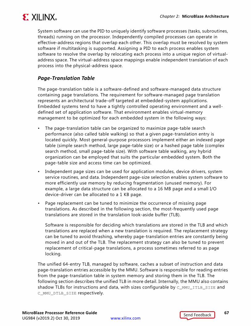
Chapter 2: MicroBlaze Architecture
System software can use the PID to uniquely identify software processes (tasks, subroutines, threads) running on the processor. Independently compiled processes can operate in effective-address regions that overlap each other. This overlap must be resolved by system software if multitasking is supported. Assigning a PID to each process enables system software to resolve the overlap by relocating each process into a unique region of virtual-address space. The virtual-address space mappings enable independent translation of each process into the physical-address space.
Page-Translation Table
The page-translation table is a software-defined and software-managed data structure containing page translations. The requirement for software-managed page translation represents an architectural trade-off targeted at embedded-system applications. Embedded systems tend to have a tightly controlled operating environment and a well-defined set of application software. That environment enables virtual-memory management to be optimized for each embedded system in the following ways:
• The page-translation table can be organized to maximize page-table search performance (also called table walking) so that a given page-translation entry is located quickly. Most general-purpose processors implement either an indexed page table (simple search method, large page-table size) or a hashed page table (complex search method, small page-table size). With software table walking, any hybrid organization can be employed that suits the particular embedded system. Both the page-table size and access time can be optimized.
• Independent page sizes can be used for application modules, device drivers, system service routines, and data. Independent page-size selection enables system software to more efficiently use memory by reducing fragmentation (unused memory). For example, a large data structure can be allocated to a 16 MB page and a small I/O device-driver can be allocated to a 1 KB page.
• Page replacement can be tuned to minimize the occurrence of missing page translations. As described in the following section, the most-frequently used page translations are stored in the translation look-aside buffer (TLB).
Software is responsible for deciding which translations are stored in the TLB and which translations are replaced when a new translation is required. The replacement strategy can be tuned to avoid thrashing, whereby page-translation entries are constantly being moved in and out of the TLB. The replacement strategy can also be tuned to prevent replacement of critical-page translations, a process sometimes referred to as page locking.
The unified 64-entry TLB, managed by software, caches a subset of instruction and data page-translation entries accessible by the MMU. Software is responsible for reading entries from the page-translation table in system memory and storing them in the TLB. The following section describes the unified TLB in more detail. Internally, the MMU also contains shadow TLBs for instructions and data, with sizes configurable by C_MMU_ITLB_SIZE and C_MMU_DTLB_SIZE respectively.
MicroBlaze Processor Reference Guide 67UG984 (v2019.2) Oct 30, 2019 www.xilinx.com
Send Feedback
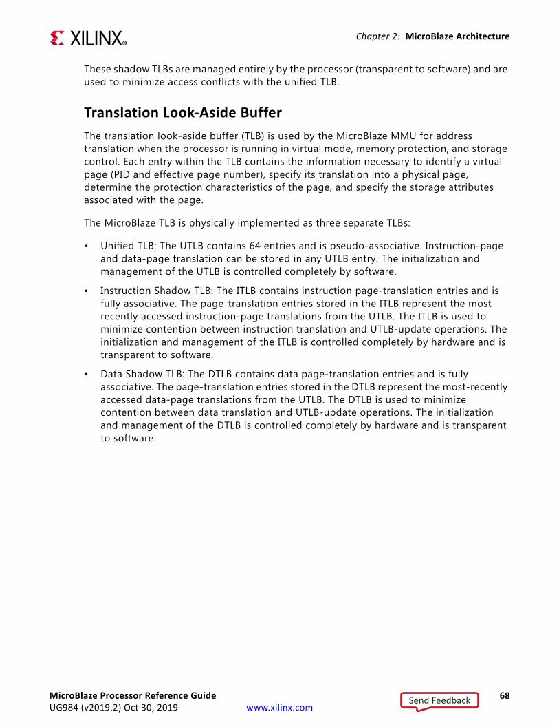
Chapter 2: MicroBlaze Architecture
These shadow TLBs are managed entirely by the processor (transparent to software) and are used to minimize access conflicts with the unified TLB.
Translation Look-Aside BufferThe translation look-aside buffer (TLB) is used by the MicroBlaze MMU for address translation when the processor is running in virtual mode, memory protection, and storage control. Each entry within the TLB contains the information necessary to identify a virtual page (PID and effective page number), specify its translation into a physical page, determine the protection characteristics of the page, and specify the storage attributes associated with the page.
The MicroBlaze TLB is physically implemented as three separate TLBs:
• Unified TLB: The UTLB contains 64 entries and is pseudo-associative. Instruction-page and data-page translation can be stored in any UTLB entry. The initialization and management of the UTLB is controlled completely by software.
• Instruction Shadow TLB: The ITLB contains instruction page-translation entries and is fully associative. The page-translation entries stored in the ITLB represent the most-recently accessed instruction-page translations from the UTLB. The ITLB is used to minimize contention between instruction translation and UTLB-update operations. The initialization and management of the ITLB is controlled completely by hardware and is transparent to software.
• Data Shadow TLB: The DTLB contains data page-translation entries and is fully associative. The page-translation entries stored in the DTLB represent the most-recently accessed data-page translations from the UTLB. The DTLB is used to minimize contention between data translation and UTLB-update operations. The initialization and management of the DTLB is controlled completely by hardware and is transparent to software.
MicroBlaze Processor Reference Guide 68UG984 (v2019.2) Oct 30, 2019 www.xilinx.com
Send Feedback

Chapter 2: MicroBlaze Architecture
The following figure provides the translation flow for TLB.
X-Ref Target - Figure 2-19
Figure 2-19: TLB Address Translation Flow
Perform DTLBLook-Up
Generate I-side Effective Address
No Translation Perform ITLBLook-Up
Translation Disabled(MSR[VM]=0)
Translation Enabled(MSR[VM]=1)
Generate D-side Effective Address
No Translation
Translation Enabled(MSR[VM]=1)
Translation Disabled(MSR[VM]=0)
ITLB Hit ITLB Miss DTLB Miss DTLB Hit
Extract Real Address from ITLB
Perform UTLBLook-Up
Extract Real Address from DTLB
Continue I-cacheAccess
Continue I-cacheor D-cache
Access
UTLB Hit UTLB Miss
Extract Real Address from UTLB I-Side TLB Miss or
D-Side TLB MissException
Route Addressto ITLB
Route Addressto DTLB
X19756-111617
MicroBlaze Processor Reference Guide 69UG984 (v2019.2) Oct 30, 2019 www.xilinx.com
Send Feedback

Chapter 2: MicroBlaze Architecture
TLB Entry Format
The following figure shows the format of a TLB entry. Each TLB entry ranges from 68 bits up to 100 bits and is composed of two portions: TLBLO (also referred to as the data entry), and TLBHI (also referred to as the tag entry).
When 64-bit MicroBlaze or the Physical Address Extension (PAE) is enabled, the TLB entry is extended with up to 32 additional bits in the TLBLO RPN field to support up to a 64 bit physical address.
The TLB entry contents are described in more detail in Table 2-21 and Table 2-22, including the TLBLO format with PAE or 64-bit MicroBlaze enabled.
The fields within a TLB entry are categorized as follows:
• Virtual-page identification (TAG, SIZE, V, TID): These fields identify the page-translation entry. They are compared with the virtual-page number during the translation process.
• Physical-page identification (RPN, SIZE): These fields identify the translated page in physical memory.
• Access control (EX, WR, ZSEL): These fields specify the type of access allowed in the page and are used to protect pages from improper accesses.
• Storage attributes (W, I, M, G, E, U0): These fields specify the storage-control attributes, such as caching policy for the data cache (write-back or write-through), whether a page is cacheable, and how bytes are ordered (endianness).
Table 2-39 shows the relationship between the TLB-entry SIZE field and the translated page size. This table also shows how the page size determines which address bits are involved in a tag comparison, which address bits are used as a page offset, and which bits in the physical page number are used in the physical address. With 64-bit MicroBlaze or PAE enabled, the most significant bits of the physical address are directly taken from the extended RPN field.
X-Ref Target - Figure 2-20
Figure 2-20: TLB Entry Format (PAE Disabled)
RPN
220 31282423
ZSEL W I G
TAG
220 3528272625
SIZE V E TID
TLBLO:
TLBHI:
29 30
M
U0
EX WR
X19757-111617
MicroBlaze Processor Reference Guide 70UG984 (v2019.2) Oct 30, 2019 www.xilinx.com
Send Feedback

Chapter 2: MicroBlaze Architecture
TLB Access
When the MMU translates a virtual address (the combination of PID and effective address) into a physical address, it first examines the appropriate shadow TLB for the page translation entry. If an entry is found, it is used to access physical memory. If an entry is not found, the MMU examines the UTLB for the entry. A delay occurs each time the UTLB must be accessed due to a shadow TLB miss. The miss latency ranges from 2-32 cycles. The DTLB has priority over the ITLB if both simultaneously access the UTLB.
Figure 2-21 shows the logical process the MMU follows when examining a page-translation entry in one of the shadow TLBs or the UTLB. All valid entries in the TLB are checked.
A TLB hit occurs when all of the following conditions are met by a TLB entry:
• The entry is valid
• The TAG field in the entry matches the effective address EPN under the control of the SIZE field in the entry
• The TID field in the entry matches the PID
If any of the above conditions are not met, a TLB miss occurs. A TLB miss causes an exception, described as follows:
A TID value of 0x00 causes the MMU to ignore the comparison between the TID and PID. Only the TAG and EA[EPN] are compared. A TLB entry with TID=0x00 represents a process-independent translation. Pages that are accessed globally by all processes should be assigned a TID value of 0x00. A PID value of 0x00 does not identify a process that can access any page. When PID=0x00, a page-translation hit only occurs when TID=0x00. It is possible for software to load the TLB with multiple entries that match an EA[EPN] and PID
Table 2-39: Page-Translation Bit Ranges by Page Size
PageSize
SIZETLBHIField
Tag ComparisonBit Range1
1. The bit index n = C_ADDR_SIZE with 64-bit MicroBlaze, and 32 otherwise.
Page Offset
PAE Disabled PAE or 64-bit Enabled2
2. The bit index n = C_ADDR_SIZE.
Physical Page
Number
RPN Bits
Clear to 0
Physical Page
NumberRPN Bits Clear to 0
1 KB 000 TAG and Address[0:n-11] Address[22:31] RPN[0:21] - RPN[0:n-11] -
4 KB 001 TAG and Address[0:n-13] Address[20:31] RPN[0:19] 20:21 RPN[0:n-13] n-12:n-11
16 KB 010 TAG and Address[0:n-15] Address[18:31] RPN[0:17] 18:21 RPN[0:n-15] n-14:n-11
64 KB 011 TAG and Address[0:n-17] Address[16:31] RPN[0:15] 16:21 RPN[0:n-17] n-16:n-11
256 KB 100 TAG and Address[0:n-19] Address[14:31] RPN[0:13] 14:21 RPN[0:n-19] n-18:n-11
1 MB 101 TAG and Address[0:n-21] Address[12:31] RPN[0:11] 12:21 RPN[0:n-21] n-20:n-11
4 MB 110 TAG and Address[0:n-23] Address[10:31] RPN[0:9] 10:21 RPN[0:n-23] n-22:n-11
16 MB 111 TAG and Address[0:n-25] Address[8:31] RPN[0:7] 8:21 RPN[0:n-25] n-24:n-11
MicroBlaze Processor Reference Guide 71UG984 (v2019.2) Oct 30, 2019 www.xilinx.com
Send Feedback

Chapter 2: MicroBlaze Architecture
combination. However, this is considered a programming error and results in undefined behavior.
When a hit occurs, the MMU reads the RPN field from the corresponding TLB entry. Some or all of the bits in this field are used, depending on the value of the SIZE field (see Table 2-39).
For example, with PAE disabled and 32-bit MicroBlaze, if the SIZE field specifies a 256 kB page size, RPN[0:13] represents the physical page number and is used to form the physical address. RPN[14:21] is not used, and software must clear those bits to 0 when initializing the TLB entry. The remainder of the physical address is taken from the page-offset portion of the EA. If the page size is 256 kB, the 32-bit physical address is formed by concatenating RPN[0:13] with bits 14:31 of the effective address.
Instead, with PAE enabled and assuming a physical address size of 40 bits (C_ADDR_SIZE set to 40), RPN[0:21] represents the physical page number and RPN[22:29] is not used. The 40-bit physical address is formed by concatenating RPN[0:21] with bits 14:31 of the effective address.
Prior to accessing physical memory, the MMU examines the TLB-entry access-control fields. These fields indicate whether the currently executing program is allowed to perform the requested memory access.
If access is allowed, the MMU checks the storage-attribute fields to determine how to access the page. The storage-attribute fields specify the caching policy for memory accesses.
TLB Access Failures
A TLB-access failure causes an exception to occur. This interrupts execution of the instruction that caused the failure and transfers control to an interrupt handler to resolve the failure. A TLB access can fail for two reasons:
• A matching TLB entry was not found, resulting in a TLB miss
• A matching TLB entry was found, but access to the page was prevented by either the storage attributes or zone protection
When an interrupt occurs, the processor enters real mode by clearing MSR[VM] to 0. In real mode, all address translation and memory-protection checks performed by the MMU are disabled. After system software initializes the UTLB with page-translation entries, management of the MicroBlaze UTLB is usually performed using interrupt handlers running in real mode.
MicroBlaze Processor Reference Guide 72UG984 (v2019.2) Oct 30, 2019 www.xilinx.com
Send Feedback

Chapter 2: MicroBlaze Architecture
The following figure diagrams the general process for examining a TLB entry.
The following sections describe the conditions under which exceptions occur due to TLB access failures.
X-Ref Target - Figure 2-21
Figure 2-21: General Process for Examining a TLB Entry
Check TLB-EntryUsing Virtual Address
TLB HI[V]=1 TLB Entry MissNo
TLBHI[TID]=0x00
Yes
CompareTLBHI[TAG] with EA[EPN]
Using TLBHI[SIZE]
CompareTLBHI[TID] with PID TLB Entry MissNo Match
Check Access Access ViolationNot allowed
Match (TLB Hit)
Allowed
Check for Guarded Storage Storage ViolationGuarded
Data Reference Instruction Fetch
Read TLBLO[RPN]Using TLBHI[SIZE]
Extract Offset from EA using TLBHI[SIZE]
Generate Physical Address from TLBLO[RPN] and Offset
Yes No
Match
TLB Entry MissNo Match
Not Guarded
X19758-111617
MicroBlaze Processor Reference Guide 73UG984 (v2019.2) Oct 30, 2019 www.xilinx.com
Send Feedback
Chapter 2: MicroBlaze Architecture
Data-Storage Exception
When virtual mode is enabled, (MSR[VM]=1), a data-storage exception occurs when access to a page is not permitted for any of the following reasons:
• From user mode:
- The TLB entry specifies a zone field that prevents access to the page (ZPR[Zn]=00). This applies to load and store instructions.
- The TLB entry specifies a read-only page (TLBLO[WR]=0) that is not otherwise overridden by the zone field (ZPR[Zn]‚ 11). This applies to store instructions.
• From privileged mode:
- The TLB entry specifies a read-only page (TLBLO[WR]=0) that is not otherwise overridden by the zone field (ZPR[Zn]‚ 10 and ZPR[Zn]‚ 11). This applies to store instructions.
Instruction-Storage Exception
When virtual mode is enabled, (MSR[VM]=1), an instruction-storage exception occurs when access to a page is not permitted for any of the following reasons:
• From user mode:
- The TLB entry specifies a zone field that prevents access to the page (ZPR[Zn]=00).
- The TLB entry specifies a non-executable page (TLBLO[EX]=0) that is not otherwise overridden by the zone field (ZPR[Zn]‚ 11).
- The TLB entry specifies a guarded-storage page (TLBLO[G]=1).
• From privileged mode:
- The TLB entry specifies a non-executable page (TLBLO[EX]=0) that is not otherwise overridden by the zone field (ZPR[Zn]‚ 10 and ZPR[Zn]‚ 11).
- The TLB entry specifies a guarded-storage page (TLBLO[G]=1).
Data TLB-Miss Exception
When virtual mode is enabled (MSR[VM]=1) a data TLB-miss exception occurs if a valid, matching TLB entry was not found in the TLB (shadow and UTLB). Any load or store instruction can cause a data TLB-miss exception.
Instruction TLB-Miss Exception
When virtual mode is enabled (MSR[VM]=1) an instruction TLB-miss exception occurs if a valid, matching TLB entry was not found in the TLB (shadow and UTLB). Any instruction fetch can cause an instruction TLB-miss exception.
MicroBlaze Processor Reference Guide 74UG984 (v2019.2) Oct 30, 2019 www.xilinx.com
Send Feedback
Chapter 2: MicroBlaze Architecture
Access ProtectionSystem software uses access protection to protect sensitive memory locations from improper access. System software can restrict memory accesses for both user-mode and privileged-mode software. Restrictions can be placed on reads, writes, and instruction fetches. Access protection is available when virtual protected mode is enabled.
Access control applies to instruction fetches, data loads, and data stores. The TLB entry for a virtual page specifies the type of access allowed to the page.
The TLB entry also specifies a zone-protection field in the zone-protection register that is used to override the access controls specified by the TLB entry.
TLB Access-Protection Controls
Each TLB entry controls three types of access:
• Process: Processes are protected from unauthorized access by assigning a unique process ID (PID) to each process. When system software starts a user-mode application, it loads the PID for that application into the PID register. As the application executes, memory addresses are translated using only TLB entries with a TID field in Translation Look-Aside Buffer High (TLBHI) that matches the PID. This enables system software to restrict accesses for an application to a specific area in virtual memory. A TLB entry with TID=0x00 represents a process-independent translation. Pages that are accessed globally by all processes should be assigned a TID value of 0x00.
• Execution: The processor executes instructions only if they are fetched from a virtual page marked as executable (TLBLO[EX]=1). Clearing TLBLO[EX] to 0 prevents execution of instructions fetched from a page, instead causing an instruction-storage interrupt (ISI) to occur. The ISI does not occur when the instruction is fetched, but instead occurs when the instruction is executed. This prevents speculatively fetched instructions that are later discarded (rather than executed) from causing an ISI.
The zone-protection register can override execution protection.
• Read/Write: Data is written only to virtual pages marked as writable (TLBLO[WR]=1). Clearing TLBLO[WR] to 0 marks a page as read-only. An attempt to write to a read-only page causes a data-storage interrupt (DSI) to occur.
The zone-protection register can override write protection.
TLB entries cannot be used to prevent programs from reading pages. In virtual mode, zone protection is used to read-protect pages. This is done by defining a no-access-allowed zone (ZPR[Zn] = 00) and using it to override the TLB-entry access protection. Only programs running in user mode can be prevented from reading a page. Privileged programs always have read access to a page.
MicroBlaze Processor Reference Guide 75UG984 (v2019.2) Oct 30, 2019 www.xilinx.com
Send Feedback
Chapter 2: MicroBlaze Architecture
Zone Protection
Zone protection is used to override the access protection specified in a TLB entry. Zones are an arbitrary grouping of virtual pages with common access protection. Zones can contain any number of pages specifying any combination of page sizes. There is no requirement for a zone to contain adjacent pages.
The zone-protection register (ZPR) is a 32-bit register used to specify the type of protection override applied to each of 16 possible zones. The protection override for a zone is encoded in the ZPR as a 2-bit field.
The 4-bit zone-select field in a TLB entry (TLBLO[ZSEL]) selects one of the 16 zone fields from the ZPR (Z0–Z15). For example, zone Z5 is selected when ZSEL = 0101.
Changing a zone field in the ZPR applies a protection override across all pages in that zone. Without the ZPR, protection changes require individual alterations to each page translation entry within the zone.
Unimplemented zones (when C_MMU_ZONES < 16) are treated as if they contained 11.
UTLB ManagementThe UTLB serves as the interface between the processor MMU and memory-management software. System software manages the UTLB to tell the MMU how to translate virtual addresses into physical addresses. When a problem occurs due to a missing translation or an access violation, the MMU communicates the problem to system software using the exception mechanism. System software is responsible for providing interrupt handlers to correct these problems so that the MMU can proceed with memory translation.
Software reads and writes UTLB entries using the MFS and MTS instructions, respectively. With PAE enabled, the MFSE and MTSE instructions are used to access the most significant part of the real page number. These instructions use the TLBX register index (numbered 0 to 63) corresponding to one of the 64 entries in the UTLB. The tag and data portions are read and written separately, so software must execute two MFS or MTS instructions, and also an additional MFSE or MTSE instruction when PAE is enabled, to completely access an entry.
With 64-bit MicroBlaze, the MFS and MTS instructions can access the entire contents of the UTLB entry directly.
The UTLB is searched for a specific translation using the TLBSX register. TLBSX locates a translation using an effective address and loads the corresponding UTLB index into the TLBX register.
Individual UTLB entries are invalidated using the MTS instruction to clear the valid bit in the tag portion of a TLB entry (TLBHI[V]).
MicroBlaze Processor Reference Guide 76UG984 (v2019.2) Oct 30, 2019 www.xilinx.com
Send Feedback

Chapter 2: MicroBlaze Architecture
When C_FAULT_TOLERANT is set to 1, the UTLB block RAM is protected by parity. In case of a parity error, a TLB miss exception occurs. To avoid accumulating errors in this case, each entry in the UTLB should be periodically invalidated.
Recording Page Access and Page ModificationSoftware management of virtual-memory poses several challenges:
• In a virtual-memory environment, software and data often consume more memory than is physically available. Some of the software and data pages must be stored outside physical memory, such as on a hard drive, when they are not used. Ideally, the most-frequently used pages stay in physical memory and infrequently used pages are stored elsewhere.
• When pages in physical-memory are replaced to make room for new pages, it is important to know whether the replaced (old) pages were modified.
If they were modified, they must be saved prior to loading the replacement (new) pages. If the old pages were not modified, the new pages can be loaded without saving the old pages.
• A limited number of page translations are kept in the UTLB. The remaining translations must be stored in the page-translation table. When a translation is not found in the UTLB (due to a miss), system software must decide which UTLB entry to discard so that the missing translation can be loaded. It is desirable for system software to replace infrequently used translations rather than frequently used translations.
Solving the above problems in an efficient manner requires keeping track of page accesses and page modifications. MicroBlaze does not track page access and page modification in hardware. Instead, system software can use the TLB-miss exceptions and the data-storage exception to collect this information. As the information is collected, it can be stored in a data structure associated with the page-translation table.
Page-access information is used to determine which pages should be kept in physical memory and which are replaced when physical-memory space is required. System software can use the valid bit in the TLB entry (TLBHI[V]) to monitor page accesses. This requires page translations be initialized as not valid (TLBHI[V]=0) to indicate they have not been accessed. The first attempt to access a page causes a TLB-miss exception, either because the UTLB entry is marked not valid or because the page translation is not present in the UTLB. The TLB-miss handler updates the UTLB with a valid translation (TLBHI[V]=1). The set valid bit serves as a record that the page and its translation have been accessed. The TLB-miss handler can also record the information in a separate data structure associated with the page-translation entry.
Page-modification information is used to indicate whether an old page can be overwritten with a new page or the old page must first be stored to a hard disk. System software can use the write-protection bit in the TLB entry (TLBLO[WR]) to monitor page modification. This requires page translations be initialized as read-only (TLBLO[WR]=0) to indicate they have
MicroBlaze Processor Reference Guide 77UG984 (v2019.2) Oct 30, 2019 www.xilinx.com
Send Feedback
Chapter 2: MicroBlaze Architecture
not been modified. The first attempt to write data into a page causes a data-storage exception, assuming the page has already been accessed and marked valid as described above. If software has permission to write into the page, the data-storage handler marks the page as writable (TLBLO[WR]=1) and returns.
The set write-protection bit serves as a record that a page has been modified. The data-storage handler can also record this information in a separate data structure associated with the page-translation entry.
Tracking page modification is useful when virtual mode is first entered and when a new process is started.
MicroBlaze Processor Reference Guide 78UG984 (v2019.2) Oct 30, 2019 www.xilinx.com
Send Feedback

Chapter 2: MicroBlaze Architecture
Reset, Interrupts, Exceptions, and BreakMicroBlaze supports reset, interrupt, user exception, break, and hardware exceptions. The following section describes the execution flow associated with each of these events.
The relative priority starting with the highest is:
1. Reset2. Hardware Exception3. Non-maskable Break4. Break5. Interrupt6. User Vector (Exception)
Table 2-40 defines the memory address locations of the associated vectors and the hardware enforced register file locations for return addresses. Each vector allocates two addresses to allow full address range branching (requires an IMM followed by a BRAI instruction). Normally the vectors start at address 0, but the parameter C_BASE_VECTORS can be used to locate them anywhere in memory.
The address range 0x28 to 0x4F is reserved for future software support by Xilinx. Allocating these addresses for user applications is likely to conflict with future releases of support software.
All of these events will clear the reservation bit, used together with the LWX and SWX instructions to implement mutual exclusion, such as semaphores and spinlocks.
Table 2-40: Vectors and Return Address Register File Location
Event Vector Address Register File Return Address
Reset C_BASE_VECTORS + 0x0 - C_BASE_VECTORS + 0x4 -
User Vector (Exception) C_BASE_VECTORS + 0x8 - C_BASE_VECTORS + 0xC Rx
Interrupt1
1. With low-latency interrupt mode, the vector address is supplied by the Interrupt Controller.
C_BASE_VECTORS + 0x10 - C_BASE_VECTORS + 0x14 R14
Break: Non-maskable hardware C_BASE_VECTORS + 0x18 -
C_BASE_VECTORS + 0x1C R16Break: Hardware
Break: Software
Hardware Exception C_BASE_VECTORS + 0x20 - C_BASE_VECTORS + 0x24 R17 or BTR
Reserved by Xilinx for future use
C_BASE_VECTORS + 0x28 - C_BASE_VECTORS + 0x4F -
MicroBlaze Processor Reference Guide 79UG984 (v2019.2) Oct 30, 2019 www.xilinx.com
Send Feedback

Chapter 2: MicroBlaze Architecture
ResetWhen a Reset or Debug_Rst (1) occurs, MicroBlaze flushes the pipeline and immediately starts fetching instructions from the reset vector (address C_BASE_VECTORS + 0x0). Both external reset signals are active high, and it is recommended to assert the signals for at least 16 cycles.
See MicroBlaze Core Configurability in Chapter 3 for more information on the MSR reset value parameters, which are used to define the initial value of the Machine Status Register.
Reset does not clear the general purpose registers (r1 - r31) or the instruction and data caches. To ensure that stale data is not used, software should not assume that the general purpose registers are zero, and the program should invalidate instruction and data caches before they are enabled. See Chapter 4, Reset Handling for a C code example of cache invalidation.
MicroBlaze does not wait for outstanding AXI or LMB transactions to complete before it begins fetching instructions from the reset vector. When only resetting the processor, all external accesses must be completed before asserting Reset. This can be achieved with an MBAR instruction to enter sleep mode or the Pause signal. See Sleep and Pause Functionality in Chapter 3 for details.
Equivalent Pseudocode
PC ← C_BASE_VECTORS + 0x0MSR ← C_RESET_MSR_IE << 2 | C_RESET_MSR_BIP << 4 | C_RESET_MSR_ICE << 6 |
C_RESET_MSR_DCE << 8 | C_RESET_MSR_EE << 9 | C_RESET_MSR_EIP << 10EAR ← 0; ESR ← 0; FSR ← 0PID ← 0; ZPR ← 0; TLBX ← 0 Reservation ← 0
Hardware ExceptionsMicroBlaze can be configured to trap the following internal error conditions: illegal instruction, instruction and data bus error, and unaligned access. The divide exception can only be enabled if the processor is configured with a hardware divider (C_USE_DIV=1).
When configured with a hardware floating-point unit (C_USE_FPU>0), it can also trap the following floating-point specific exceptions: underflow, overflow, float division-by-zero, invalid operation, and denormalized operand error.
When configured with a hardware memory management unit (MMU), it can also trap the following memory management specific exceptions: Illegal Instruction Exception, Data Storage Exception, Instruction Storage Exception, Data TLB Miss Exception, and Instruction TLB Miss Exception.
1. Reset input controlled by the debugger using MDM.
MicroBlaze Processor Reference Guide 80UG984 (v2019.2) Oct 30, 2019 www.xilinx.com
Send Feedback
Chapter 2: MicroBlaze Architecture
A hardware exception causes MicroBlaze to flush the pipeline and branch to the hardware exception vector (address C_BASE_VECTORS + 0x20). The execution stage instruction in the exception cycle is not executed.
The exception also updates the general purpose register R17 in the following manner:
• For the MMU exceptions (Data Storage Exception, Instruction Storage Exception, Data TLB Miss Exception, Instruction TLB Miss Exception) the register R17 is loaded with the appropriate program counter value to re-execute the instruction causing the exception upon return. The value is adjusted to return to a preceding IMM instruction, if any. If the exception is caused by an instruction in a branch delay slot, the value is adjusted to return to the branch instruction, including adjustment for a preceding IMM instruction, if any.
• For all other exceptions the register R17 is loaded with the program counter value of the subsequent instruction, unless the exception is caused by an instruction in a branch delay slot. If the exception is caused by an instruction in a branch delay slot, the ESR[DS] bit is set. In this case the exception handler should resume execution from the branch target address stored in BTR.
The EE and EIP bits in MSR are automatically reverted when executing the RTED instruction.
The VM and UM bits in MSR are automatically reverted from VMS and UMS when executing the RTED, RTBD, and RTID instructions.
Exception Priority
When two or more exceptions occur simultaneously, they are handled in the following order, from the highest priority to the lowest:
• Instruction Bus Exception
• Instruction TLB Miss Exception
• Instruction Storage Exception
• Illegal Opcode Exception
• Privileged Instruction Exception or Stack Protection Violation Exception
• Data TLB Miss Exception
• Data Storage Exception
• Unaligned Exception
• Data Bus Exception
• Divide Exception
• FPU Exception
• Stream Exception
MicroBlaze Processor Reference Guide 81UG984 (v2019.2) Oct 30, 2019 www.xilinx.com
Send Feedback

Chapter 2: MicroBlaze Architecture
Exception Causes
• Stream Exception: The AXI4-Stream exception is caused by executing a get or getd instruction with the ‘e’ bit set to ‘1’ when there is a control bit mismatch.
• Instruction Bus Exception: The instruction bus exception is caused by errors when reading data from memory.
- The instruction peripheral AXI4 interface (M_AXI_IP) exception is caused by an error response on M_AXI_IP_RRESP.
- The instruction cache AXI4 interface (M_AXI_IC) exception is caused by an error response on M_AXI_IC_RRESP. The exception can only occur when the parameter C_ICACHE_ALWAYS_USED is set to 1 and the cache is turned off, or if the MMU Inhibit Caching bit is set for the address. In all other cases the response is ignored.
- The instructions side local memory (ILMB) can only cause instruction bus exception when either an uncorrectable error occurs in the LMB memory, as indicated by the IUE signal, or C_ECC_USE_CE_EXCEPTION is set to 1 and a correctable error occurs in the LMB memory, as indicated by the ICE signal.
• Illegal Opcode Exception: The illegal opcode exception is caused by an instruction with an invalid major opcode (bits 0 through 5 of instruction). Bits 6 through 31 of the instruction are not checked. Optional processor instructions are detected as illegal if not enabled. If the optional feature C_OPCODE_0x0_ILLEGAL is enabled, an illegal opcode exception is also caused if the instruction is equal to 0x00000000.
• Data Bus Exception: The data bus exception is caused by errors when reading data from memory or writing data to memory.
- The data peripheral AXI4 interface (M_AXI_DP) exception is caused by an error response on M_AXI_DP_RRESP or M_AXI_DP_BRESP.
- The data cache AXI4 interface (M_AXI_DC) exception is caused by:
- An error response on M_AXI_DC_RRESP or M_AXI_DC_BRESP,
- OKAY response on M_AXI_DC_RRESP in case of an exclusive access using LWX.
The exception can only occur when C_DCACHE_ALWAYS_USED is set to 1 and the cache is turned off, when an exclusive access using LWX or SWX is performed, or if the MMU Inhibit Caching bit is set for the address. In all other cases the response is ignored.
- The data side local memory (DLMB) can only cause instruction bus exception when either an uncorrectable error occurs in the LMB memory, as indicated by the DUE signal, or C_ECC_USE_CE_EXCEPTION is set to 1 and a correctable error occurs in the
MicroBlaze Processor Reference Guide 82UG984 (v2019.2) Oct 30, 2019 www.xilinx.com
Send Feedback

Chapter 2: MicroBlaze Architecture
LMB memory, as indicated by the DCE signal. An error can occur for all read accesses, and for byte and halfword write accesses.
• Unaligned Exception: For 32-bit MicroBlaze the unaligned exception is caused by a word access where the address to the data bus has any of the two least significant bits set, or a half-word access with the least significant bit set.
For 64-bit MicroBlaze the unaligned exception is caused by a long access where the address to the data bus has any of the three least significant bits set, a word access with any of the two least significant bits set, or a half-word access with the least significant bit set.
• Divide Exception: The divide exception is caused by an integer division (idiv or idivu) where the divisor is zero, or by a signed integer division (idiv) where overflow occurs (-2147483648 / -1).
• FPU Exception: An FPU exception is caused by an underflow, overflow, divide-by-zero, illegal operation, or denormalized operand occurring with a floating-point instruction.
- Underflow occurs when the result is denormalized.
- Overflow occurs when the result is not-a-number (NaN).
- The divide-by-zero FPU exception is caused by the rA operand to fdiv being zero when rB is not infinite.
- Illegal operation is caused by a signaling NaN operand or by illegal infinite or zero operand combinations.
• Privileged Instruction Exception: The Privileged Instruction exception is caused by an attempt to execute a privileged instruction in User Mode.
• Stack Protection Violation Exception: A Stack Protection Violation exception is caused by executing a load or store instruction using the stack pointer (register R1) as rA with an address outside the stack boundaries defined by the special Stack Low and Stack High registers, causing a stack overflow or a stack underflow.
• Data Storage Exception: The Data Storage exception is caused by an attempt to access data in memory that results in a memory-protection violation.
• Instruction Storage Exception: The Instruction Storage exception is caused by an attempt to access instructions in memory that results in a memory-protection violation.
• Data TLB Miss Exception: The Data TLB Miss exception is caused by an attempt to access data in memory, when a valid Translation Look-Aside Buffer entry is not present, and virtual protected mode is enabled.
MicroBlaze Processor Reference Guide 83UG984 (v2019.2) Oct 30, 2019 www.xilinx.com
Send Feedback

Chapter 2: MicroBlaze Architecture
• Instruction TLB Miss Exception: The Instruction TLB Miss exception is caused by an attempt to access instructions in memory, when a valid Translation Look-Aside Buffer entry is not present, and virtual protected mode is enabled.
Should an Instruction Bus Exception, Illegal Opcode Exception, or Data Bus Exception occur when C_FAULT_TOLERANT is set to 1, and an exception is in progress (that is MSR[EIP] set and MSR[EE] cleared), the pipeline is halted, and the external signal MB_Error is set.
Imprecise Exceptions
Normally all exceptions in MicroBlaze are precise, meaning that any instructions in the pipeline after the instruction causing an exception are invalidated, and have no effect.
When C_IMPRECISE_EXCEPTIONS is set to 1 (ECC) an Instruction Bus Exception or Data Bus Exception caused by ECC errors in LMB memory is not precise, meaning that a subsequent memory access instruction in the pipeline might be executed. If this behavior is acceptable, the maximum frequency can be improved by setting this parameter to 1.
Equivalent Pseudocode
ESR[DS] ← exception in delay slotif ESR[DS] then
BTR ← branch target PCif MMU exception then
if branch preceded by IMM thenr17 ← PC - 8
elser17 ← PC - 4
elser17 ← invalid value
else if MMU exception thenif instruction preceded by IMM then
r17 ← PC - 4else
r17 ← PCelse
r17 ← PC + 4PC ← C_BASE_VECTORS + 0x20MSR[EE] ← 0, MSR[EIP]← 1MSR[UMS] ← MSR[UM], MSR[UM] ← 0, MSR[VMS] ← MSR[VM], MSR[VM] ← 0ESR[EC] ← exception specific valueESR[ESS]← exception specific valueEAR ← exception specific valueFSR ← exception specific value Reservation ← 0
BreaksThere are two kinds of breaks:
• Hardware (external) breaks
MicroBlaze Processor Reference Guide 84UG984 (v2019.2) Oct 30, 2019 www.xilinx.com
Send Feedback

Chapter 2: MicroBlaze Architecture
• Software (internal) breaks
Hardware Breaks
Hardware breaks are performed by asserting the external break signal (that is, the Ext_BRK and Ext_NM_BRK input ports). On a break, the instruction in the execution stage completes while the instruction in the decode stage is replaced by a branch to the break vector (address C_BASE_VECTORS + 0x18).
The break return address (the PC associated with the instruction in the decode stage at the time of the break) is automatically loaded into general purpose register R16. MicroBlaze also sets the Break In Progress (BIP) flag in the Machine Status Register (MSR).
A normal hardware break (that is, the Ext_BRK input port) is only handled when MSR[BIP] and MSR[EIP] are set to 0 (that is, there is no break or exception in progress). The Break In Progress flag disables interrupts. A non-maskable break (that is, the Ext_NM_BRK input port) is always handled immediately.
The BIP bit in the MSR is automatically cleared when executing the RTBD instruction.
The Ext_BRK signal must be kept asserted until the break has occurred, and deasserted before the RTBD instruction is executed. The Ext_NM_BRK signal must only be asserted one clock cycle.
Software Breaks
To perform a software break, use the brk and brki instructions. Refer to Chapter 5, MicroBlaze Instruction Set Architecture for detailed information on software breaks.
As a special case, when C_DEBUG_ENABLED is greater than zero, and “brki rD,0x18” is executed, a software breakpoint is signaled to the debugger; for example, the Xilinx System Debugger (XSDB) tool, irrespective of the value of C_BASE_VECTORS. In this case the BIP bit in the MSR is not set.
Latency
The time it takes the MicroBlaze processor to enter a break service routine from the time the break occurs depends on the instruction currently in the execution stage and the latency to the memory storing the break vector.
Equivalent Pseudocode
r16 ← PCPC ← C_BASE_VECTORS + 0x18MSR[BIP] ← 1
MicroBlaze Processor Reference Guide 85UG984 (v2019.2) Oct 30, 2019 www.xilinx.com
Send Feedback
Chapter 2: MicroBlaze Architecture
MSR[UMS] ← MSR[UM], MSR[UM] ← 0, MSR[VMS] ← MSR[VM], MSR[VM] ← 0 Reservation ← 0
InterruptMicroBlaze supports one external interrupt source (connected to the Interrupt input port). The processor only reacts to interrupts if the Interrupt Enable (IE) bit in the Machine Status Register (MSR) is set to 1. On an interrupt, the instruction in the execution stage completes while the instruction in the decode stage is replaced by a branch to the interrupt vector. This is either address C_BASE_VECTORS + 0x10, or with low-latency interrupt mode, the address supplied by the Interrupt Controller.
The interrupt return address (the PC associated with the instruction in the decode stage at the time of the interrupt) is automatically loaded into general purpose register R14. In addition, the processor also disables future interrupts by clearing the IE bit in the MSR. The IE bit is automatically set again when executing the RTID instruction.
Interrupts are ignored by the processor if either of the break in progress (BIP) or exception in progress (EIP) bits in the MSR are set to 1.
By using the parameter C_INTERRUPT_IS_EDGE, the external interrupt can either be set to level-sensitive or edge-triggered:
• When using level-sensitive interrupts, the Interrupt input must remain set until MicroBlaze has taken the interrupt, and jumped to the interrupt vector. Software must acknowledge the interrupt at the source to clear it before returning from the interrupt handler. If not, the interrupt is taken again, as soon as interrupts are enabled when returning from the interrupt handler.
• When using edge-triggered interrupts, MicroBlaze detects and latches the Interrupt input edge, which means that the input only needs to be asserted one clock cycle. The interrupt input can remain asserted, but must be deasserted at least one clock cycle before a new interrupt can be detected. The latching of an edge-triggered interrupt is independent of the IE bit in MSR. Should an interrupt occur while the IE bit is 0, it will immediately be serviced when the IE bit is set to 1.
With periodic interrupt sources, such as the FIT Timer IP core, that do not have a method to clear the interrupt from software, it is recommended to use edge-triggered interrupts.
Low-latency Interrupt Mode
A low-latency interrupt mode is available, which allows the Interrupt Controller to directly supply the interrupt vector for each individual interrupt (using the Interrupt_Address input port). The address of each fast interrupt handler must be passed to the Interrupt
MicroBlaze Processor Reference Guide 86UG984 (v2019.2) Oct 30, 2019 www.xilinx.com
Send Feedback

Chapter 2: MicroBlaze Architecture
Controller when initializing the interrupt system. When a particular interrupt occurs, this address is supplied by the Interrupt Controller, which allows MicroBlaze to directly jump to the handler code.
With this mode, MicroBlaze also directly sends the appropriate interrupt acknowledge to the Interrupt Controller (using the Interrupt_Ack output port), although it is still the responsibility of the Interrupt Service Routine to acknowledge level sensitive interrupts at the source.
This information allows the Interrupt Controller to acknowledge interrupts appropriately, both for level-sensitive and edge-triggered interrupt.
To inform the Interrupt Controller of the interrupt handling events, Interrupt_Ack is set to:
• 01: When MicroBlaze jumps to the interrupt handler code,
• 10: When the RTID instruction is executed to return from interrupt,
• 11: When MSR[IE] is changed from 0 to 1, which enables interrupts again.
The Interrupt_Ack output port is active during one clock cycle, and is then reset to 00.
Latency
The time it takes MicroBlaze to enter an Interrupt Service Routine (ISR) from the time an interrupt occurs, depends on the configuration of the processor and the latency of the memory controller storing the interrupt vectors. If MicroBlaze is configured to have a hardware divider, the largest latency happens when an interrupt occurs during the execution of a division instruction.
With low-latency interrupt mode, the time to enter the ISR is significantly reduced, since the interrupt vector for each individual interrupt is directly supplied by the Interrupt Controller. With compiler support for fast interrupts, there is no need for a common ISR at all. Instead, the ISR for each individual interrupt will be directly called, and the compiler takes care of saving and restoring registers used by the ISR.
Equivalent Pseudocoder14 ← PCif C_USE_INTERRUPT = 2PC ← Interrupt_AddressInterrupt_Ack ← 01
elsePC ← C_BASE_VECTORS + 0x10
MSR[IE] ← 0MSR[UMS] ← MSR[UM], MSR[UM] ← 0, MSR[VMS] ← MSR[VM], MSR[VM] ← 0 Reservation ← 0
MicroBlaze Processor Reference Guide 87UG984 (v2019.2) Oct 30, 2019 www.xilinx.com
Send Feedback

Chapter 2: MicroBlaze Architecture
User Vector (Exception)The user exception vector is located at address 0x8. A user exception is caused by inserting a ‘BRALID Rx,0x8’ instruction in the software flow. Although Rx could be any general purpose register, Xilinx recommends using R15 for storing the user exception return address, and to use the RTSD instruction to return from the user exception handler.
Pseudocode
rx ← PCPC ← C_BASE_VECTORS + 0x8MSR[UMS] ← MSR[UM], MSR[UM] ← 0, MSR[VMS] ← MSR[VM], MSR[VM] ← 0 Reservation ← 0
MicroBlaze Processor Reference Guide 88UG984 (v2019.2) Oct 30, 2019 www.xilinx.com
Send Feedback
Chapter 2: MicroBlaze Architecture
Instruction Cache
OverviewMicroBlaze can be used with an optional instruction cache for improved performance when executing code that resides outside the LMB address range.
The instruction cache has the following features:
• Direct mapped (1-way associative)
• User selectable cacheable memory address range
• Configurable cache and tag size
• Caching over AXI4 interface (M_AXI_IC)
• Option to use 4, 8 or 16 word cache-line
• Cache on and off controlled using a bit in the MSR
• Optional WIC instruction to invalidate instruction cache lines
• Optional stream buffers to improve performance by speculatively prefetching instructions
• Optional victim cache to improve performance by saving evicted cache lines
• Optional parity protection that invalidates cache lines if a Block RAM bit error is detected
• Optional data width selection to either use 32 bits, an entire cache line, or 512 bits
General Instruction Cache FunctionalityWhen the instruction cache is used, the memory address space is split into two segments: a cacheable segment and a non-cacheable segment. The cacheable segment is determined by two parameters: C_ICACHE_BASEADDR and C_ICACHE_HIGHADDR. All addresses within this range correspond to the cacheable address segment. All other addresses are non-cacheable.
The cacheable segment size must be 2N, where N is a positive integer. The range specified by C_ICACHE_BASEADDR and C_ICACHE_HIGHADDR must comprise a complete power-of-two range, such that range = 2N and the N least significant bits of C_ICACHE_BASEADDR must be zero.
The cacheable instruction address consists of two parts: the cache address, and the tag address. The MicroBlaze instruction cache can be configured from 64 bytes to 64 kB. This corresponds to a cache address of between 6 and 16 bits. The tag address together with the cache address should match the full address of cacheable memory.
MicroBlaze Processor Reference Guide 89UG984 (v2019.2) Oct 30, 2019 www.xilinx.com
Send Feedback

Chapter 2: MicroBlaze Architecture
When selecting cache sizes below 2 kB, distributed RAM is used to implement the Tag RAM and Instruction RAM. Distributed RAM is always used to implement the Tag RAM, when setting the parameter C_ICACHE_FORCE_TAG_LUTRAM to 1. This parameter is only available with cache size 8 kB and less for 4 word cache-lines, with 16 kB and less for 8 word cache-lines, and with 32 kB and less for 16 word cache-lines.
For example: in a 32-bit MicroBlaze configured with C_ICACHE_BASEADDR= 0x00300000, C_ICACHE_HIGHADDR=0x0030ffff, C_CACHE_BYTE_SIZE=4096, C_ICACHE_LINE_LEN=8, and C_ICACHE_FORCE_TAG_LUTRAM=0; the cacheable memory of 64 kB uses 16 bits of byte address, and the 4 kB cache uses 12 bits of byte address, thus the required address tag width is: 16-12=4 bits. The total number of block RAM primitives required in this configuration is: 2 RAMB16 for storing the 1024 instruction words, and 1 RAMB16 for 128 cache line entries, each consisting of: 4 bits of tag, 8 word-valid bits, 1 line-valid bit. In total 3 RAMB16 primitives.
The following figure shows the organization of Instruction Cache.
Instruction Cache OperationFor every instruction fetched, the instruction cache detects if the instruction address belongs to the cacheable segment. If the address is non-cacheable, the cache controller ignores the instruction and lets the M_AXI_IP or LMB complete the request. If the address is cacheable, a lookup is performed on the tag memory to check if the requested address is currently cached. The lookup is successful if: the word and line valid bits are set, and the tag address matches the instruction address tag segment. On a cache miss, the cache controller requests the new instruction over the instruction AXI4 interface (M_AXI_IC), and waits for the memory controller to return the associated cache line.
C_ICACHE_DATA_WIDTH determines the bus data width, either 32 bits, an entire cache line (128, 256 or 512 bits), or 512 bits.
X-Ref Target - Figure 2-22
Figure 2-22: Instruction Cache Organization
Tag Address Cache Address
Instruction Address Bits
- -
=TagRAM
Line Addr Tag
Valid (word and line)Cache_Hit
InstructionRAM
Word AddrCache_instruction_data
30 310
X19759-111617
MicroBlaze Processor Reference Guide 90UG984 (v2019.2) Oct 30, 2019 www.xilinx.com
Send Feedback
Chapter 2: MicroBlaze Architecture
When C_FAULT_TOLERANT is set to 1, a cache miss also occurs if a parity error is detected in a tag or instruction Block RAM.
The instruction cache issues burst accesses for the AXI4 interface when 32-bit data width is used, otherwise single accesses are used.
Stream Buffers
When stream buffers are enabled, by setting the parameter C_ICACHE_STREAMS to 1, the cache will speculatively fetch cache lines in advance in sequence following the last requested address, until the stream buffer is full.
The stream buffer can hold up to two cache lines. Should the processor subsequently request instructions from a cache line prefetched by the stream buffer, which occurs in linear code, they are immediately available.
The stream buffer often improves performance, since the processor generally has to spend less time waiting for instructions to be fetched from memory.
C_ICACHE_DATA_WIDTH determines the amount of data transferred from the stream buffer each clock cycle, either 32 bits or an entire cache line.
To be able to use instruction cache stream buffers, area optimization must not be enabled.
Victim Cache
The victim cache is enabled by setting the parameter C_ICACHE_VICTIMS to 2, 4 or 8. This defines the number of cache lines that can be stored in the victim cache. Whenever a cache line is evicted from the cache, it is saved in the victim cache. By saving the most recent lines they can be fetched much faster, should the processor request them, thereby improving performance. If the victim cache is not used, all evicted cache lines must be read from memory again when they are needed.
C_ICACHE_DATA_WIDTH determines the amount of data transferred from/to the victim cache each clock cycle, either 32 bits or an entire cache line.
Note: To be able to use the victim cache, area optimization must not be enabled.
Instruction Cache Software Support
MSR Bit
The ICE bit in the MSR provides software control to enable and disable caches.
The contents of the cache are preserved by default when the cache is disabled. You can invalidate cache lines using the WIC instruction or using the hardware debug logic of MicroBlaze.
MicroBlaze Processor Reference Guide 91UG984 (v2019.2) Oct 30, 2019 www.xilinx.com
Send Feedback

Chapter 2: MicroBlaze Architecture
WIC Instruction
The optional WIC instruction (C_ALLOW_ICACHE_WR=1) is used to invalidate cache lines in the instruction cache from an application. For a detailed description, see Chapter 5, MicroBlaze Instruction Set Architecture.
The WIC instruction can also be used together with parity protection to periodically invalidate entries the cache, to avoid accumulating errors.
MicroBlaze Processor Reference Guide 92UG984 (v2019.2) Oct 30, 2019 www.xilinx.com
Send Feedback
Chapter 2: MicroBlaze Architecture
Data Cache
OverviewThe MicroBlaze processor can be used with an optional data cache for improved performance. The cached memory range must not include addresses in the LMB address range. The data cache has the following features:
• Direct mapped (1-way associative)
• Write-through or Write-back
• User selectable cacheable memory address range
• Configurable cache size and tag size
• Caching over AXI4 interface (M_AXI_DC)
• Option to use 4, 8 or 16 word cache-lines
• Cache on and off controlled using a bit in the MSR
• Optional WDC instruction to invalidate or flush data cache lines
• Optional victim cache with write-back to improve performance by saving evicted cache lines
• Optional parity protection for write-through cache that invalidates cache lines if a Block RAM bit error is detected
• Optional data width selection to either use 32 bits, an entire cache line, or 512 bits
General Data Cache FunctionalityWhen the data cache is used, the memory address space is split into two segments: a cacheable segment and a non-cacheable segment. The cacheable area is determined by two parameters: C_DCACHE_BASEADDR and C_DCACHE_HIGHADDR. All addresses within this range correspond to the cacheable address space. All other addresses are non-cacheable.
The cacheable segment size must be 2N, where N is a positive integer. The range specified by C_DCACHE_BASEADDR and C_DCACHE_HIGHADDR must comprise a complete power-of-two range, such that range = 2N and the N least significant bits of C_DCACHE_BASEADDR must be zero.
MicroBlaze Processor Reference Guide 93UG984 (v2019.2) Oct 30, 2019 www.xilinx.com
Send Feedback

Chapter 2: MicroBlaze Architecture
The following figure shows the Data Cache organization.
The cacheable data address consists of two parts: the cache address, and the tag address. The MicroBlaze data cache can be configured from 64 bytes to 64 kB. This corresponds to a cache address of between 6 and 16 bits. The tag address together with the cache address should match the full address of cacheable memory. When selecting cache sizes below 2 kB, distributed RAM is used to implement the Tag RAM and Data RAM, except that block RAM is always used for the Data RAM when C_AREA_OPTIMIZED is set to 1 (Area) and C_DCACHE_USE_WRITEBACK is not set. Distributed RAM is always used to implement the Tag RAM, when setting the parameter C_DCACHE_FORCE_TAG_LUTRAM to 1. This parameter is only available with cache size 8 kB and less for 4 word cache-lines, with 16 kB and less for 8 word cache-lines, and with 32 kB and less for 16 word cache-lines.
For example, in a 32-bit MicroBlaze configured with C_DCACHE_BASEADDR=0x00400000, C_DCACHE_HIGHADDR=0x00403fff, C_DCACHE_BYTE_SIZE=2048, C_DCACHE_LINE_LEN=4, and C_DCACHE_FORCE_TAG_LUTRAM=0; the cacheable memory of 16 kB uses 14 bits of byte address, and the 2 kB cache uses 11 bits of byte address, thus the required address tag width is 14-11=3 bits. The total number of block RAM primitives required in this configuration is 1 RAMB16 for storing the 512 data words, and 1 RAMB16 for 128 cache line entries, each consisting of 3 bits of tag, 4 word-valid bits, 1 line-valid bit. In total, 2 RAMB16 primitives.
Data Cache OperationThe caching policy used by the MicroBlaze data cache, write-back or write-through, is determined by the parameter C_DCACHE_USE_WRITEBACK. When this parameter is set, a write-back protocol is implemented; otherwise write-through is implemented.
However, when configured with an MMU (C_USE_MMU > 1, C_AREA_OPTIMIZED = 0 (Performance) or 2 (Frequency), C_DCACHE_USE_WRITEBACK = 1), the caching policy in virtual mode is determined by the W storage attribute in the TLB entry, whereas write-back is used in real mode.
X-Ref Target - Figure 2-23
Figure 2-23: Data Cache Organization
Tag Address Cache Word Address
Data Address Bits
- -
=TagRAM
Addr Tag
Valid Cache_Hit
DataRAM
Addr Cache_data
Load_Instruction
0 30 31
X19760-111617
MicroBlaze Processor Reference Guide 94UG984 (v2019.2) Oct 30, 2019 www.xilinx.com
Send Feedback

Chapter 2: MicroBlaze Architecture
With the write-back protocol, a store to an address within the cacheable range always updates the cached data. If the target address word is not in the cache (that is, the access is a cache miss), and the location in the cache contains data that has not yet been written to memory (the cache location is dirty), the old data is written over the data AXI4 interface (M_AXI_DC) to external memory before updating the cache with the new data. If only a single word needs to be written, a single word write is used, otherwise a burst write is used. For byte or halfword stores, in case of a cache miss, the address is first requested over the data AXI4 interface, while a word store only updates the cache.
With the write-through protocol, a store to an address within the cacheable range generates an equivalent byte, halfword, or word write over the data AXI4 interface to external memory. The write also updates the cached data if the target address word is in the cache (that is, the write is a cache hit). A write cache-miss does not load the associated cache line into the cache.
Provided that the cache is enabled a load from an address within the cacheable range triggers a check to determine if the requested data is currently cached. If it is (that is, on a cache hit) the requested data is retrieved from the cache. If not (that is, on a cache miss) the address is requested over the data AXI4 interface using a burst read, and the processor pipeline stalls until the cache line associated to the requested address is returned from the external memory controller.
The parameter C_DCACHE_DATA_WIDTH determines the bus data width, either 32 bits, an entire cache line (128, 256 or 512 bits), or 512 bits.
When C_FAULT_TOLERANT is set to 1 and write-through protocol is used, a cache miss also occurs if a parity error is detected in the tag or data block RAM.
MicroBlaze Processor Reference Guide 95UG984 (v2019.2) Oct 30, 2019 www.xilinx.com
Send Feedback

Chapter 2: MicroBlaze Architecture
The following table summarizes all types of accesses issued by the data cache AXI4 interface.
Victim Cache
The victim cache is enabled by setting the parameter C_DCACHE_VICTIMS to 2, 4 or 8. This defines the number of cache lines that can be stored in the victim cache. Whenever a complete cache line is evicted from the cache, it is saved in the victim cache. By saving the most recent lines they can be fetched much faster, should the processor request them, thereby improving performance. If the victim cache is not used, all evicted cache lines must be read from memory again when they are needed.
With the AXI4 interface, C_DCACHE_DATA_WIDTH determines the amount of data transferred from/to the victim cache each clock cycle, either 32 bits or an entire cache line.
Note: To be able to use the victim cache, write-back must be enabled and area optimization must not be enabled.
Data Cache Software Support
MSR Bit
The DCE bit in the MSR controls whether or not the cache is enabled. When disabling caches the user must ensure that all the prior writes within the cacheable range have been completed in external memory before reading back over M_AXI_DP. This can be done by writing to a semaphore immediately before turning off caches, and then in a loop poll until it has been written. The contents of the cache are preserved when the cache is disabled.
Table 2-41: Data Cache Interface Accesses
Policy State Direction Access Type
Write-through
Cache Enabled
Read Burst for 32-bit interface non-exclusive access and exclusive access with ACE enabled, single access otherwise
Write Single access
Cache Disabled
Read Burst for 32-bit interface exclusive access with ACE enabled, single access otherwise
Write Single access
Write-back Cache Enabled
Read Burst for 32-bit interface, single access otherwise
Write Burst for 32-bit interface cache lines with more than one valid word, a single access otherwise
Cache Disabled
Read Burst for 32-bit interface non-exclusive access, discarding all but the desired data, a single access otherwise
Write Single access
MicroBlaze Processor Reference Guide 96UG984 (v2019.2) Oct 30, 2019 www.xilinx.com
Send Feedback

Chapter 2: MicroBlaze Architecture
WDC Instruction
The optional WDC instruction (C_ALLOW_DCACHE_WR=1) is used to invalidate or flush cache lines in the data cache from an application. For a detailed description, please refer to Chapter 5, MicroBlaze Instruction Set Architecture.
The WDC instruction can also be used together with parity protection to periodically invalidate entries the cache, to avoid accumulating errors.
With an external L2 cache, such as the System Cache, connected to MicroBlaze using the ACE interface, external cache invalidate or flush can be performed with WDC. See the System Cache LogiCORE IP Product Guide (PG118) [Ref 6] for more information on the System Cache.
MicroBlaze Processor Reference Guide 97UG984 (v2019.2) Oct 30, 2019 www.xilinx.com
Send Feedback

Chapter 2: MicroBlaze Architecture
Floating-Point Unit (FPU)
OverviewThe MicroBlaze floating-point unit is based on the IEEE 754-1985 standard [Ref 18]:
• Uses IEEE 754 single precision floating-point format, and double precision format with 64-bit MicroBlaze, including definitions for infinity, not-a-number (NaN), and zero
• Supports addition, subtraction, multiplication, division, comparison, conversion and square root instructions
• Implements round-to-nearest mode
• Generates sticky status bits for: underflow, overflow, divide-by-zero and invalid operation
For improved performance, the following non-standard simplifications are made:
• Denormalized (1) operands are not supported. A hardware floating-point operation on a denormalized number returns a quiet NaN and sets the sticky denormalized operand error bit in FSR; see Floating-Point Status Register (FSR).
• A denormalized result is stored as a signed 0 with the underflow bit set in FSR. This method is commonly referred to as Flush-to-Zero (FTZ)
• An operation on a quiet NaN returns the fixed NaN: 0xFFC00000 for single precision or 0xFFF8000000000000 for double precision, rather than one of the NaN operands
• Overflow as a result of a floating-point operation always returns signed ∞
Format
Single Precision
An IEEE 754 single precision floating-point number is composed of the following three fields:
1. 1-bit sign
2. 8-bit biased exponent
3. 23-bit fraction (a.k.a. mantissa or significand)
The fields are stored in a 32 bit word as defined in the following figure:
1. Numbers that are so close to 0, that they cannot be represented with full precision, that is, any number n that falls in the following ranges for single precision: (1.17549*10-38 > n > 0), or (0 > n > -1.17549 * 10-38), and the following ranges for double precision: (5.562684646268*10-309 > n > 0), or (0 > n > -5.562684646268 * 10-309)
MicroBlaze Processor Reference Guide 98UG984 (v2019.2) Oct 30, 2019 www.xilinx.com
Send Feedback
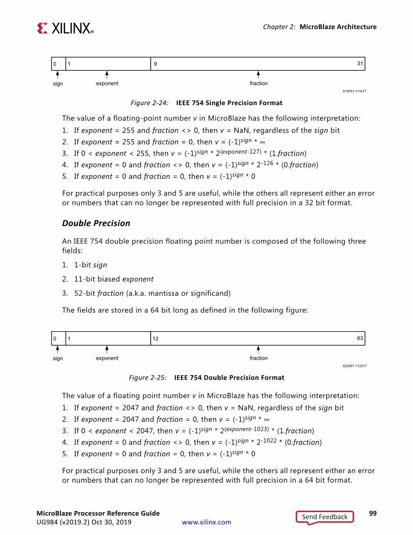
Chapter 2: MicroBlaze Architecture
The value of a floating-point number v in MicroBlaze has the following interpretation:
1. If exponent = 255 and fraction <> 0, then v = NaN, regardless of the sign bit2. If exponent = 255 and fraction = 0, then v = (-1)sign * ∞3. If 0 < exponent < 255, then v = (-1)sign * 2(exponent-127) * (1.fraction)4. If exponent = 0 and fraction <> 0, then v = (-1)sign * 2-126 * (0.fraction) 5. If exponent = 0 and fraction = 0, then v = (-1)sign * 0
For practical purposes only 3 and 5 are useful, while the others all represent either an error or numbers that can no longer be represented with full precision in a 32 bit format.
Double Precision
An IEEE 754 double precision floating point number is composed of the following three fields:
1. 1-bit sign
2. 11-bit biased exponent
3. 52-bit fraction (a.k.a. mantissa or significand)
The fields are stored in a 64 bit long as defined in the following figure:
The value of a floating point number v in MicroBlaze has the following interpretation:
1. If exponent = 2047 and fraction <> 0, then v = NaN, regardless of the sign bit2. If exponent = 2047 and fraction = 0, then v = (-1)sign * ∞3. If 0 < exponent < 2047, then v = (-1)sign * 2(exponent-1023) * (1.fraction)4. If exponent = 0 and fraction <> 0, then v = (-1)sign * 2-1022 * (0.fraction) 5. If exponent = 0 and fraction = 0, then v = (-1)sign * 0
For practical purposes only 3 and 5 are useful, while the others all represent either an error or numbers that can no longer be represented with full precision in a 64 bit format.
X-Ref Target - Figure 2-24
Figure 2-24: IEEE 754 Single Precision Format
319
fractionexponent
10
signX19761-111617
X-Ref Target - Figure 2-25
Figure 2-25: IEEE 754 Double Precision Format
6312
fractionexponent
10
sign
MicroBlaze Processor Reference Guide 99UG984 (v2019.2) Oct 30, 2019 www.xilinx.com
Send Feedback

Chapter 2: MicroBlaze Architecture
RoundingThe MicroBlaze FPU only implements the default rounding mode, “Round-to-nearest”, specified in IEEE 754. By definition, the result of any floating-point operation should return the nearest single precision value to the infinitely precise result. If the two nearest representable values are equally near, then the one with its least significant bit zero is returned.
OperationsAll MicroBlaze FPU operations use the processors general purpose registers rather than a dedicated floating-point register file, see General Purpose Registers.
Arithmetic
The FPU implements the following floating point operations, where the double operations are available with 64-bit MicroBlaze:
• addition, fadd and dadd
• subtraction, frsub and drsub
• multiplication, fmul and dmul
• division, fdiv and ddiv
• square root, fsqrt and dsqrt (available if C_USE_FPU = 2, EXTENDED)
Comparison
The FPU implements the following floating point comparisons, where the double operations are available with 64-bit MicroBlaze:
• compare less-than, fcmp.lt and dcmp.lt
• compare equal, fcmp.eq and dcmp.eq
• compare less-or-equal, fcmp.le and dcmp.le
• compare greater-than, fcmp.gt and dcmp.gt
• compare not-equal, fcmp.ne and dcmp.ne
• compare greater-or-equal, fcmp.ge and dcmp.ge
• compare unordered, fcmp.un and dcmp.un (used for NaN)
Conversion
The FPU implements the following conversions (available if C_USE_FPU = 2, EXTENDED), where the double operations are available with 64-bit MicroBlaze:
MicroBlaze Processor Reference Guide 100UG984 (v2019.2) Oct 30, 2019 www.xilinx.com
Send Feedback
Chapter 2: MicroBlaze Architecture
• convert from signed integer to single floating point, flt
• convert from single floating point to signed integer, fint
• convert from signed long to floating point, dbl
• convert from double floating point to signed long, dlong
ExceptionsThe floating-point unit uses the regular hardware exception mechanism in MicroBlaze. When enabled, exceptions are thrown for all the IEEE standard conditions: underflow, overflow, divide-by-zero, and illegal operation, as well as for the MicroBlaze specific exception: denormalized operand error.
A floating-point exception inhibits the write to the destination register (Rd). This allows a floating-point exception handler to operate on the uncorrupted register file.
Software SupportThe Vitis™ compiler system, based on GCC, provides support for the floating-point Unit compliant with the MicroBlaze API. Compiler flags are automatically added to the GCC command line based on the type of FPU present in the system, when using Vitis.
All double-precision operations are emulated in software with 32-bit MicroBlaze. Be aware that the xil_printf() function does not support floating-point output. The standard C library printf() and related functions do support floating-point output, but will increase the program code size.
Libraries and Binary Compatibility
The Vitis compiler system only includes software floating-point C runtime libraries. To take advantage of the hardware FPU, the libraries must be recompiled with the appropriate compiler switches.
For all cases where separate compilation is used, it is very important that you ensure the consistency of FPU compiler flags throughout the build.
Operator Latencies
The latencies of the various operations supported by the FPU are listed in Chapter 5, “MicroBlaze Instruction Set Architecture.” The FPU instructions are not pipelined, so only one operation can be ongoing at any time.
C Language Programming
To gain maximum benefit from the FPU without low-level assembly-language programming, it is important to consider how the C compiler will interpret your source
MicroBlaze Processor Reference Guide 101UG984 (v2019.2) Oct 30, 2019 www.xilinx.com
Send Feedback

Chapter 2: MicroBlaze Architecture
code. Very often the same algorithm can be expressed in many different ways, and some are more efficient than others.
Immediate Constants
Floating-point constants in C are double-precision by default. When using a single-precision FPU, careless coding could result in double-precision software emulation routines being used instead of the native single-precision instructions. To avoid this, explicitly specify (by cast or suffix) that immediate constants in your arithmetic expressions are single-precision values.
For example:
float x = 0.0;...x += (float)1.0; /* float addition */x += 1.0F; /* alternative to above */x += 1.0; /* warning - uses double addition! */
Note that the GNU C compiler can be instructed to treat all floating-point constants as single-precision (contrary to the ANSI C standard) by supplying the compiler flag -fsingle-precision-constants.
Avoiding Unnecessary Casting
While conversions between floating-point and integer formats are supported in hardware by the FPU, when C_USE_FPU is set to 2 (Extended), it is still best to avoid them when possible.
The following not-recommended example calculates the sum of squares of the integers from 1 to 10 using floating-point representation:
float sum, t;int i;sum = 0.0f;for (i = 1; i <= 10; i++) {t = (float)i;sum += t * t;
}
The above code requires a cast from an integer to a float on each loop iteration. This can be rewritten as:
float sum, t;int i;t = sum = 0.0f;for(i = 1; i <= 10; i++) {t += 1.0f;sum += t * t;
}
Note: The compiler is not at liberty to perform this optimization in general, as the two code fragments above might give different results in some cases (for example, very large t).
MicroBlaze Processor Reference Guide 102UG984 (v2019.2) Oct 30, 2019 www.xilinx.com
Send Feedback
Chapter 2: MicroBlaze Architecture
Using Square Root Runtime Library Function
The standard C runtime math library functions operate using double-precision arithmetic. When using a single-precision FPU, calls to the square root functions (sqrt()) result in inefficient emulation routines being used instead of FPU instructions:
#include <math.h>...float x=-1.0F;...x = sqrt(x); /* uses double precision */
Here the math.h header is included to avoid a warning message from the compiler.
When used with single-precision data types, the result is a cast to double, a runtime library call is made (which does not use the FPU) and then a truncation back to float is performed.
The solution is to use the non-ANSI function sqrtf() instead, which operates using single precision and can be carried out using the FPU. For example:
#include <math.h>...float x=-1.0F;...x = sqrtf(x); /* uses single precision */
Note: When compiling this code, the compiler flag -fno-math-errno (in addition to -mhard-float and -mxl-float-sqrt) must be used, to ensure that the compiler does not generate unnecessary code to handle error conditions by updating the errno variable.
MicroBlaze Processor Reference Guide 103UG984 (v2019.2) Oct 30, 2019 www.xilinx.com
Send Feedback

Chapter 2: MicroBlaze Architecture
Stream Link InterfacesMicroBlaze can be configured with up to 16 AXI4-Stream interfaces, each consisting of one input and one output port. The channels are dedicated uni-directional point-to-point data streaming interfaces.
For detailed information on the AXI4-Stream interface, please refer to the AMBA 4 AXI4-Stream Protocol Specification, Version 1.0 (Arm IHI 0051A) [Ref 14] document.
The interfaces on MicroBlaze are 32 bits wide. A separate bit indicates whether the sent/received word is of control or data type. The get instruction in the MicroBlaze ISA is used to transfer information from a port to a general purpose register. The put instruction is used to transfer data in the opposite direction. Both instructions come in 4 flavors: blocking data, non-blocking data, blocking control, and non-blocking control. For a detailed description of the get and put instructions, see Chapter 5, MicroBlaze Instruction Set Architecture.
Hardware AccelerationEach link provides a low latency dedicated interface to the processor pipeline. Thus they are ideal for extending the processors execution unit with custom hardware accelerators. A simple example is illustrated in the following figure. The code uses RFSLx to indicate the used link.
This method is similar to extending the ISA with custom instructions, but has the benefit of not making the overall speed of the processor pipeline dependent on the custom function. Also, there are no additional requirements on the software tool chain associated with this type of functional extension.
X-Ref Target - Figure 2-26
Figure 2-26: Stream Link Used with HW Accelerated Function fx
MicroBlaze
Link x
// Configure fx
cput Rc, RFSLx
// Store operands
put Ra, RFSLx // op 1
put Rb, RFSLx // op 2
// Load result
RegisterFile
Custom HW Accelerator
Op 1 Reg Op 2 Reg
ConfigReg
fx
Result RegLink x
X19783-111617
MicroBlaze Processor Reference Guide 104UG984 (v2019.2) Oct 30, 2019 www.xilinx.com
Send Feedback

Chapter 2: MicroBlaze Architecture
Debug and Trace
Debug OverviewMicroBlaze features a debug interface to support JTAG based software debugging tools (commonly known as BDM or Background Debug Mode debuggers) like the Xilinx System Debugger (XSDB) tool. The debug interface is designed to be connected to the Xilinx Microprocessor Debug Module (MDM) core, which interfaces with the JTAG port of Xilinx FPGAs. Multiple MicroBlaze instances can be interfaced with a single MDM to enable multiprocessor debugging.
To be able to download programs, set software breakpoints and disassemble code, the instruction and data memory ranges must overlap, and use the same physical memory.
Debug registers are accessed using the debug interface, and are not directly visible to software running on the processor, unless the MDM is configured to enable software access to user-accessible debug registers. The debug interface can either use JTAG serial access or AXI4-Lite parallel access, controlled by the parameter C_DEBUG_INTERFACE.
See the MicroBlaze Debug Module (MDM) Product Guide (PG115) [Ref 4] for a detailed description of the MDM features.
The basic debugging features enabled by setting C_DEBUG_ENABLED to 1 (Basic) include:
• Configurable number of hardware breakpoints and watchpoints and unlimited software breakpoints
• External processor control enables debug tools to stop, reset, and single step MicroBlaze
• Read from and write to: memory, general purpose registers, and special purpose register, except EAR, EDR, ESR, BTR and PVR0 - PVR12, which can only be read
• Support for multiple processors
The extended debugging features enabled by setting C_DEBUG_ENABLED to 2 (Extended) include:
• Configurable number of performance monitoring event and latency counters
• Program Trace:
- Embedded program trace with configurable trace buffer size
- External program trace for multiple processors, provided by the MDM
• Non-intrusive profiling support with configurable profiling buffer size
• Cross trigger support between multiple processors, and external cross trigger inputs and outputs, provided by the MDM
MicroBlaze Processor Reference Guide 105UG984 (v2019.2) Oct 30, 2019 www.xilinx.com
Send Feedback
Chapter 2: MicroBlaze Architecture
Performance MonitoringWith extended debugging, MicroBlaze provides performance monitoring counters to count various events and to measure latency during program execution. The number of event counters and latency counters can be configured with C_DEBUG_EVENT_COUNTERS and C_DEBUG_LATENCY_COUNTERS respectively, and the counter width can be set to 32, 48 or 64 bits with C_DEBUG_COUNTER_WIDTH. With the default configuration, the counter width is set to 32 bits and there are five event counters and one latency counter.
An event counter simply counts the number of times a certain event has occurred, whereas a latency counter provides the following information:
• Number of times the event has occurred (N)
• The sum of each event latency measured by counting clock cycles from the event starts until it finishes (ΣL), used to calculate the mean latency
• The sum of each event latency squared (ΣL2), used to calculate the latency standard deviation
• The minimum, shortest, measured latency for all events (Lmin)
• The maximum, longest, measured latency for all events (Lmax)
The mean latency (μ) is calculated by the formula:
The standard deviation (σ) of the latency is calculated by the formula:
Counting can be started or stopped using the Performance Counter Command Register or by cross trigger events (see Table 2-63).
When configuring, reading or writing counters, they are accessed sequentially through the performance counter registers. After every access the selected counter item is incremented.
All counters are sampled simultaneously for reading using the Performance Counter Command Register. This can be done while counting, or after counting has been stopped.
When an event counter reaches its maximum value, the overflow status bit is set, and the external interrupt signal Dbg_Intr is set to one. The interrupt signal is reset to zero by clearing the counters using the Performance Counter Command Register.
By using one of the event counters to count number of clock cycles, and initializing this counter to overflow after a predetermined sampling interval, the external interrupt can be used to periodically sample the performance counters.
The available events are described in Table 2-42, listed in numerical order.
μ ΣLN-------=
σ NΣL2 ΣL( )2–
N-----------------------------------------=
MicroBlaze Processor Reference Guide 106UG984 (v2019.2) Oct 30, 2019 www.xilinx.com
Send Feedback

Chapter 2: MicroBlaze Architecture
A typical procedure to follow when initializing and using the performance monitoring counters is delineated in the steps below.
1. Initialize the events to be monitored:
- Use the Performance Command Register (Table 2-45) to reset the selected counter to the first counter, by setting the Reset bit.
- Write the desired event numbers for all counters in order, using the Performance Control Register (Table 2-44). With the default configuration this means writing the register five times for the event counters and then once for the latency counter.
2. Clear all counters and start monitoring using the Performance Command Register, by setting the Clear and Start bits.
3. Run the program or function to be monitored.
4. Sample counters and stop monitoring using the Performance Command Register, by setting the Sample and Stop bits.
5. Read the results from all counters:
- Use the Performance Command Register to reset the selected counter to the first counter, by setting the Reset bit.
- Read the status for all counters in order, using the Performance Counter Status Register (Table 2-46). With the default configuration this means reading the register five times for the event counters and then once for the latency counter. Ensure that the result is valid by checking that the overflow and full bits are not set.
- Use the Performance Command Register to reset the selected counter to the first counter, by setting the Reset bit.
- Read the counter items for all counters in order, using the Performance Counter Data Read Register (Table 2-47). With the default configuration this means reading the register five times for the event counters and then four times for the latency counter as described in Table 2-48.
6. Calculate the final results, depending on the measured events, for example:
- Use the formulas above to determine the mean latency and standard deviation for any measured latency.
- The clock cycles per instruction (CPI) can be calculated by E30 / E0.
- The instruction and data cache hit rates can be calculated by E11 / E10 and E47 / E46.
- The instruction cache miss latency is determined by (E60(ΣL) - E60(N)) / (E10 - E11), and equivalent formulas can be used to determine the data cache read and write miss latencies.
- The ratio of floating-point instructions in a program is E29/E0.
MicroBlaze Processor Reference Guide 107UG984 (v2019.2) Oct 30, 2019 www.xilinx.com
Send Feedback

Chapter 2: MicroBlaze Architecture
Table 2-42: MicroBlaze Performance Monitoring Events
Event Description Event Description
Event Counter Events
0 Any valid instruction executed 29 Floating-point (fadd, ..., fsqrt)
1 Load word (lw, lwi, lwx) executed 30 Number of clock cycles
2 Load halfword (lhu, lhui) executed 31 Immediate (imm) executed
3 Load byte (lbu, lbui) executed 32 Pattern compare (pcmpbf, pcmpeq, pcmpne)
4 Store word (sw, swi, swx) executed 33 Sign extend instructions (sext8, sext16) executed
5 Store halfword (sh, shi) executed 34 Instruction cache invalidate (wic) executed
6 Store byte (sb, sbi) executed 35 Data cache invalidate or flush (wdc) executed
7 Unconditional branch (br, bri, brk, brki) executed 36 Machine status instructions (msrset, msrclr)
8 Taken conditional branch (beq, ..., bnei) executed 37 Unconditional branch with delay slot executed
9 Not taken conditional branch (beq,..., bnei) executed
38 Taken conditional branch with delay slot executed
10 Data request from instruction cache 39 Not taken conditional branch with delay slot
11 Hit in instruction cache 40 Delay slot with no operation instruction executed
12 Read data requested from data cache 41 Load instruction (lbu, ..., lwx) executed
13 Read data hit in data cache 42 Store instruction (sb, ..., swx) executed
14 Write data request to data cache 43 MMU data access request
15 Write data hit in data cache 44 Conditional branch (beq, ..., bnei) executed
16 Load (lbu, ..., lwx) with r1 as operand executed 45 Branch (br, bri, brk, brki, beq, ..., bnei) executed
17 Store (sb, ..., swx) with r1 as operand executed 46 Read or write data request from/to data cache
18 Logical operation (and, andn, or, xor) executed 47 Read or write data cache hit
19 Arithmetic operation (add, idiv, mul, rsub) executed
48 MMU exception taken
20 Multiply operation (mul, mulh, mulhu, mulhsu, muli)
49 MMU instruction side exception taken
21 Barrel shifter operation (bsrl, bsra, bsll) executed
50 MMU data side exception taken
22 Shift operation (sra, src, srl) executed 51 Pipeline stalled
23 Exception taken 52 Branch target cache hit for a branch or return
24 Interrupt occurred 53 MMU instruction side access request
25 Pipeline stalled due to operand fetch stage (OF) 54 MMU instruction TLB (ITLB) hit
26 Pipeline stalled due to execute stage (EX) 55 MMU data TLB (DTLB) hit
27 Pipeline stalled due to memory stage (MEM) 56 MMU unified TLB (UTLB) hit
28 Integer divide (idiv, idivu) executed
Latency and Event Counter events
57 Interrupt latency from input to interrupt vector 61 MMU address lookup latency
58 Data cache latency for memory read 62 Peripheral AXI interface data read latency
MicroBlaze Processor Reference Guide 108UG984 (v2019.2) Oct 30, 2019 www.xilinx.com
Send Feedback
Chapter 2: MicroBlaze Architecture
The debug registers used to configure and control performance monitoring, and to read or write the event and latency counters, are listed in Table 2-43. All of these registers except the Performance Counter Command register are accessed repeatedly to read or write information, first for all of the event counters followed by all of the latency counters.
The DBG_CTRL value indicates the value to use in the MDM Debug Register Access Control Register to access the register, used with MDM software access to debug registers.
Performance Counter Control Register
The Performance Counter Control Register (PCCTRLR) is used to define the events that are counted by the configured performance counters. To define the events for all configured counters, the register should be written repeatedly for each of the counters. This register is a write-only register. Issuing a read request has no effect, and undefined data is read.
Every time the register is written, the selected counter is incremented. By using the Performance Counter Command Register, the selected counter can be reset to the first counter again. See the following figure and table.
59 Data cache latency for memory write 63 Peripheral AXI interface data write latency
60 Instruction cache latency for memory read
Table 2-42: MicroBlaze Performance Monitoring Events (Cont’d)
Event Description Event Description
Table 2-43: MicroBlaze Performance Monitoring Debug Registers
Register Name Size (bits) MDM Command
DBG_CTRL Value R/W Description
Performance Counter Control 8 0101 0001 4A207 W Select event for each configured
counter, according to Table 2-42
Performance Counter Command 5 0101 0010 4A404 W Command to clear counters, start or
stop counting, or sample counters
Performance Counter Status 2 0101 0011 4A601 R Read the sampled status for each
configured performance counter
Performance Counter Data Read 32 0101 0110 4AC1F R Read the sampled values for each
configured performance counter
Performance Counter Data Write 32 0101 0111 4AE1F W Write initial values for each
configured performance counter
X-Ref Target - Figure 2-27
Figure 2-27: Performance Counter Control Register
07
EventReserved
31 8
X19762-111617
MicroBlaze Processor Reference Guide 109UG984 (v2019.2) Oct 30, 2019 www.xilinx.com
Send Feedback
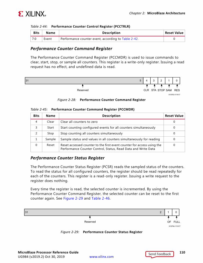
Chapter 2: MicroBlaze Architecture
Performance Counter Command Register
The Performance Counter Command Register (PCCMDR) is used to issue commands to clear, start, stop, or sample all counters. This register is a write-only register. Issuing a read request has no effect, and undefined data is read.
Performance Counter Status Register
The Performance Counter Status Register (PCSR) reads the sampled status of the counters. To read the status for all configured counters, the register should be read repeatedly for each of the counters. This register is a read-only register. Issuing a write request to the register does nothing.
Every time the register is read, the selected counter is incremented. By using the Performance Counter Command Register, the selected counter can be reset to the first counter again. See Figure 2-29 and Table 2-46.
Table 2-44: Performance Counter Control Register (PCCTRLR)
Bits Name Description Reset Value
7:0 Event Performance counter event, according to Table 2-42. 0
X-Ref Target - Figure 2-28
Figure 2-28: Performance Counter Command Register
04
RESReserved
31 5 3 2 1
SAMSTOPSTACLRX19763-111617
Table 2-45: Performance Counter Command Register (PCCMDR)
Bits Name Description Reset Value
4 Clear Clear all counters to zero 0
3 Start Start counting configured events for all counters simultaneously 0
2 Stop Stop counting all counters simultaneously 0
1 Sample Sample status and values in all counters simultaneously for reading 0
0 Reset Reset accessed counter to the first event counter for access using the Performance Counter Control, Status, Read Data and Write Data
0
X-Ref Target - Figure 2-29
Figure 2-29: Performance Counter Status Register
0
FULLReserved
31 2 1
OFX19764-111617
MicroBlaze Processor Reference Guide 110UG984 (v2019.2) Oct 30, 2019 www.xilinx.com
Send Feedback

Chapter 2: MicroBlaze Architecture
Performance Counter Data Read Register
The Performance Counter Data Read Register (PCDRR) reads the sampled values of the counters. To read the values of all configured counters, the register should be read repeatedly. This register is a read-only register. Issuing a write request to the register does nothing.
See the following figure and table.
Because a counter can have more than 32 bits, depending on the configuration, the register might need to be read repeatedly to retrieve all information for a particular counter. This is detailed in Table 2-48.
Table 2-46: Performance Counter Status Register (PCSR)
Bits Name Description Reset Value
1 Overflow This bit is set when the counter has counted past its maximum value 0
0 Full This bit is set when a new latency counter event is started before the previous event has finished. This indicates that the accuracy of the measured values is reduced.
0
X-Ref Target - Figure 2-30
Figure 2-30: Performance Counter Data Read Register
0
Item
31
X19765-111617
Table 2-47: Performance Counter Data Read Register (PCDRR)
Bits Name Description Reset Value
31:0 Item Sampled counter value item 0
Table 2-48: Performance Counter Data Items
Counter Type Item Description
C_DEBUG_COUNTER_WIDTH = 32
Event Counter 1 The number of times the event occurred
Latency Counter 1 The number of times the event occurred
2 The sum of each event latency
3 The sum of each event latency squared
4 31:16
15:0
Minimum measured latency, 16 bits
Maximum measured latency, 16 bits
MicroBlaze Processor Reference Guide 111UG984 (v2019.2) Oct 30, 2019 www.xilinx.com
Send Feedback
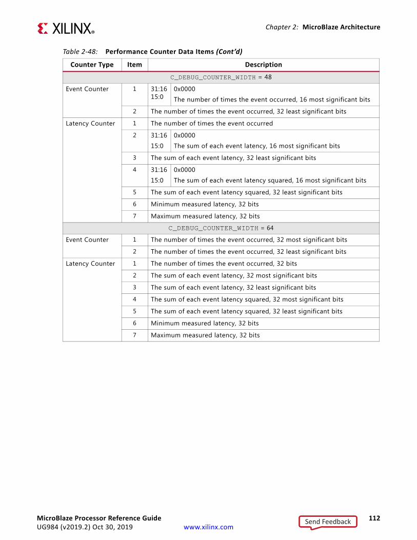
Chapter 2: MicroBlaze Architecture
C_DEBUG_COUNTER_WIDTH = 48
Event Counter 1 31:1615:0
0x0000
The number of times the event occurred, 16 most significant bits
2 The number of times the event occurred, 32 least significant bits
Latency Counter 1 The number of times the event occurred
2 31:16
15:0
0x0000
The sum of each event latency, 16 most significant bits
3 The sum of each event latency, 32 least significant bits
4 31:16
15:0
0x0000
The sum of each event latency squared, 16 most significant bits
5 The sum of each event latency squared, 32 least significant bits
6 Minimum measured latency, 32 bits
7 Maximum measured latency, 32 bits
C_DEBUG_COUNTER_WIDTH = 64
Event Counter 1 The number of times the event occurred, 32 most significant bits
2 The number of times the event occurred, 32 least significant bits
Latency Counter 1 The number of times the event occurred, 32 bits
2 The sum of each event latency, 32 most significant bits
3 The sum of each event latency, 32 least significant bits
4 The sum of each event latency squared, 32 most significant bits
5 The sum of each event latency squared, 32 least significant bits
6 Minimum measured latency, 32 bits
7 Maximum measured latency, 32 bits
Table 2-48: Performance Counter Data Items (Cont’d)
Counter Type Item Description
MicroBlaze Processor Reference Guide 112UG984 (v2019.2) Oct 30, 2019 www.xilinx.com
Send Feedback

Chapter 2: MicroBlaze Architecture
Performance Counter Data Write Register
The Performance Counter Data Write Register (PCDWR) writes initial values to the counters. To write all configured counters, the register should be written repeatedly. This register is a write-only register. Issuing a read request has no effect, and undefined data is read.
Since a counter can have more than 32 bits, depending on the configuration, the register might need to be written repeatedly to update all information for a particular counter, as described in Table 2-48.
X-Ref Target - Figure 2-31
Figure 2-31: Performance Counter Data Write Register
0
Item
31
X19766-111617
Table 2-49: Performance Counter Data Write Register (PCDWR)
Bits Name Description Reset Value
31:0 Item Counter value item to write into a counter 0
MicroBlaze Processor Reference Guide 113UG984 (v2019.2) Oct 30, 2019 www.xilinx.com
Send Feedback
Chapter 2: MicroBlaze Architecture
Program and Event TraceWith extended debugging, MicroBlaze provides program and event trace, either storing information in the Embedded Trace Buffer or transmitting it to the MDM, to enable program execution tracing. The MDM is used when the parameter C_DEBUG_EXTERNAL_TRACE is set, allowing output of program trace from multiple processors using external interfaces.
The size of the Embedded Trace Buffer can be configured from 8KB to 128KB using the parameter C_DEBUG_TRACE_SIZE. The default buffer size with external trace is 8KB, but it can also be configured from 32B to 256B to use distributed RAM. It is recommended to always keep the default 8KB size, unless block RAM resources are very scarce. By setting C_DEBUG_TRACE_SIZE to 0 (None), program trace is disabled.
Program trace uses compression to reduce the amount of trace data, while still allowing reconstruction of the program execution flow or the entire processor software state. There are three main compression levels:
• Complete trace: Stores complete trace information including cycle count for each executed instruction using 144 bits, ranging from 512 to 8192 items depending on the configured Embedded Trace Buffer size. Complete trace is not available when C_DEBUG_EXTERNAL_TRACE is set or with 64-bit MicroBlaze (C_DATA_SIZE = 64).
• Program flow: Stores program flow changes, that is the sequence of branches taken or not taken, and the new program counter for indirect branches, interrupts, exceptions and hardware breaks.
The program counter can also optionally be stored for return instructions to simplify program flow reconstruction, or for all taken branches to handle self-modifying code.
Data read from memory or fetched from AXI4-Stream interfaces might optionally be stored to allow reconstructing the entire processor software state, enabling reverse single step functionality. When the data access instruction is in a delay slot of a dynamic branch or return, the data is stored first followed by the branch target program counter. For data access instructions in delay slots of static branches, the program flow change is first saved followed by the data.
Events representing all program exceptions, interrupts, and breaks, as well as all cross-trigger events defined in Table 2-63 are also stored, to allow unambiguous decoding of program flow changes. Each event is preceded by a stored program counter.
Software can inject an event by using an “xori r0, rN, IMM” instruction. Typically this is used to trace operating system events like context switches and system calls, but it can be used by any program to trace significant events.
• Program flow and cycle count: Stores the cycle count between instructions along with the same information as program flow alone, to also allow reconstruction of the program execution time.
MicroBlaze Processor Reference Guide 114UG984 (v2019.2) Oct 30, 2019 www.xilinx.com
Send Feedback
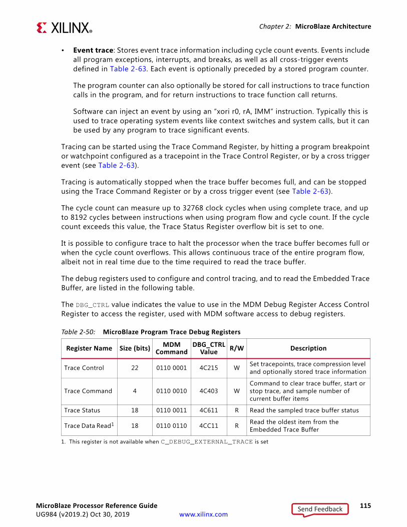
Chapter 2: MicroBlaze Architecture
• Event trace: Stores event trace information including cycle count events. Events include all program exceptions, interrupts, and breaks, as well as all cross-trigger events defined in Table 2-63. Each event is optionally preceded by a stored program counter.
The program counter can also optionally be stored for call instructions to trace function calls in the program, and for return instructions to trace function call returns.
Software can inject an event by using an “xori r0, rA, IMM” instruction. Typically this is used to trace operating system events like context switches and system calls, but it can be used by any program to trace significant events.
Tracing can be started using the Trace Command Register, by hitting a program breakpoint or watchpoint configured as a tracepoint in the Trace Control Register, or by a cross trigger event (see Table 2-63).
Tracing is automatically stopped when the trace buffer becomes full, and can be stopped using the Trace Command Register or by a cross trigger event (see Table 2-63).
The cycle count can measure up to 32768 clock cycles when using complete trace, and up to 8192 cycles between instructions when using program flow and cycle count. If the cycle count exceeds this value, the Trace Status Register overflow bit is set to one.
It is possible to configure trace to halt the processor when the trace buffer becomes full or when the cycle count overflows. This allows continuous trace of the entire program flow, albeit not in real time due to the time required to read the trace buffer.
The debug registers used to configure and control tracing, and to read the Embedded Trace Buffer, are listed in the following table.
The DBG_CTRL value indicates the value to use in the MDM Debug Register Access Control Register to access the register, used with MDM software access to debug registers.
Table 2-50: MicroBlaze Program Trace Debug Registers
Register Name Size (bits) MDM Command
DBG_CTRL Value R/W Description
Trace Control 22 0110 0001 4C215 W Set tracepoints, trace compression level and optionally stored trace information
Trace Command 4 0110 0010 4C403 WCommand to clear trace buffer, start or stop trace, and sample number of current buffer items
Trace Status 18 0110 0011 4C611 R Read the sampled trace buffer status
Trace Data Read1
1. This register is not available when C_DEBUG_EXTERNAL_TRACE is set
18 0110 0110 4CC11 R Read the oldest item from the Embedded Trace Buffer
MicroBlaze Processor Reference Guide 115UG984 (v2019.2) Oct 30, 2019 www.xilinx.com
Send Feedback

Chapter 2: MicroBlaze Architecture
Trace Control Register
The Trace Control Register (TCTRLR) is used to define the trace behavior. This register is a write-only register. Issuing a read request has no effect, and undefined data is read. See the following figure and table.
Trace Command Register
The Trace Command Register (TCMDR) is used to issue commands to clear, start, or stop trace, as well as sample the number of trace items. This register is a write-only register. Issuing a read request has no effect, and undefined data is read. See the following figure and table.
X-Ref Target - Figure 2-32
Figure 2-32: Trace Control Register
04
Reserved
31 3 2 1
SRSLSPCFH
22 521 6
Tracepoint LevelX19767-111617
Table 2-51: Trace Control Register (TCTRLR)
Bits Name Description Reset Value
21:6 Tracepoint Change corresponding breakpoint or watchpoint to a tracepoint 0
5:4 Level Trace compression level:
00 = Complete trace, not available with C_DEBUG_EXTERNAL_TRACE
01 = Program flow
10 = Event
11 = Program flow and cycle count
00
3 Full Halt Debug Halt on full trace buffer or cycle count overflow 0
2 Save PC Level 01 and 11: Save new program counter for all taken branches
Level 10: Save new program counter for all function calls
0
1 Save Load Save load and get instruction new data value 0
0 Save Return Save new program counter for return instructions 0
X-Ref Target - Figure 2-33
Figure 2-33: Trace Command Register
04
Reserved
31 3 2 1
SAMSTOPSTACLR
X19768-111617
MicroBlaze Processor Reference Guide 116UG984 (v2019.2) Oct 30, 2019 www.xilinx.com
Send Feedback

Chapter 2: MicroBlaze Architecture
Trace Status Register
The Trace Status Register (TSR) can be used to determine if trace has been started or not, to check for cycle count overflow and to read the sampled number of items in the Embedded Trace Buffer. This register is a read-only register. Issuing a write request to the register does nothing. See the following figure and table.
Trace Data Read Register
The Trace Data Read Register (TDRR) contains the oldest item read from the Embedded Trace Buffer. When the register has been read, the next item is read from the trace buffer. It is an error to read more items than are available in the trace buffer, as indicated by the item count in the Trace Status Register. This register is a read-only register. Issuing a write request to the register does nothing. See the following figure and table.
Table 2-52: Trace Command Register (TCMDR)
Bits Name Description Reset Value
3 Clear Clear trace status and empty the trace buffer 0
2 Start Start trace immediately 0
1 Stop Stop trace immediately 0
0 Sample Sample the number of current items in the trace buffer 0
X-Ref Target - Figure 2-34
Figure 2-34: Trace Status Register
0
Reserved
31 18
Item Count
17
STA
16
OF
15
X19769-111617
Table 2-53: Trace Status Register (TSR)
Bits Name Description Reset Value
17 Started Trace started, set to one when trace is started and cleared to zero when it is stopped
0
16 Overflow Cycle count overflow, set to one when the cycle count overflows, and cleared to zero by the Clear command
0
15:0 Item Count Sampled trace buffer item count 0x0000
X-Ref Target - Figure 2-35
Figure 2-35: Trace Data Read Register
0
Reserved
31 18
Buffer Value
17
X19770-111617
MicroBlaze Processor Reference Guide 117UG984 (v2019.2) Oct 30, 2019 www.xilinx.com
Send Feedback
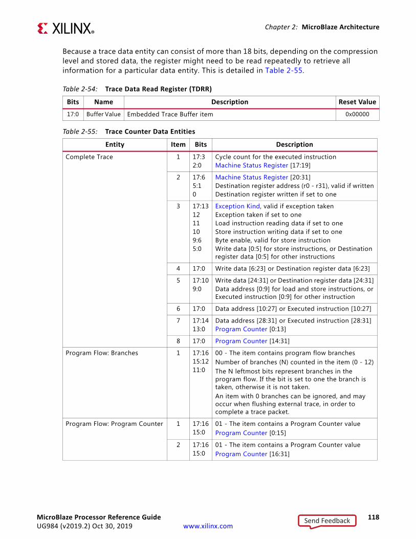
Chapter 2: MicroBlaze Architecture
Because a trace data entity can consist of more than 18 bits, depending on the compression level and stored data, the register might need to be read repeatedly to retrieve all information for a particular data entity. This is detailed in Table 2-55.
Table 2-54: Trace Data Read Register (TDRR)
Bits Name Description Reset Value
17:0 Buffer Value Embedded Trace Buffer item 0x00000
Table 2-55: Trace Counter Data Entities
Entity Item Bits Description
Complete Trace 1 17:32:0
Cycle count for the executed instructionMachine Status Register [17:19]
2 17:65:10
Machine Status Register [20:31]Destination register address (r0 - r31), valid if writtenDestination register written if set to one
3 17:131211109:65:0
Exception Kind, valid if exception takenException taken if set to oneLoad instruction reading data if set to oneStore instruction writing data if set to oneByte enable, valid for store instructionWrite data [0:5] for store instructions, or Destination register data [0:5] for other instructions
4 17:0 Write data [6:23] or Destination register data [6:23]
5 17:109:0
Write data [24:31] or Destination register data [24:31]Data address [0:9] for load and store instructions, or Executed instruction [0:9] for other instruction
6 17:0 Data address [10:27] or Executed instruction [10:27]
7 17:1413:0
Data address [28:31] or Executed instruction [28:31]Program Counter [0:13]
8 17:0 Program Counter [14:31]
Program Flow: Branches 1 17:1615:1211:0
00 - The item contains program flow branchesNumber of branches (N) counted in the item (0 - 12)The N leftmost bits represent branches in the program flow. If the bit is set to one the branch is taken, otherwise it is not taken.An item with 0 branches can be ignored, and may occur when flushing external trace, in order to complete a trace packet.
Program Flow: Program Counter 1 17:1615:0
01 - The item contains a Program Counter valueProgram Counter [0:15]
2 17:1615:0
01 - The item contains a Program Counter value Program Counter [16:31]
MicroBlaze Processor Reference Guide 118UG984 (v2019.2) Oct 30, 2019 www.xilinx.com
Send Feedback
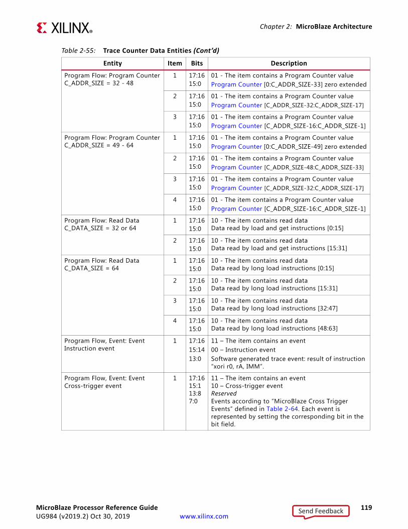
Chapter 2: MicroBlaze Architecture
Program Flow: Program Counter C_ADDR_SIZE = 32 - 48
1 17:1615:0
01 - The item contains a Program Counter valueProgram Counter [0:C_ADDR_SIZE-33] zero extended
2 17:1615:0
01 - The item contains a Program Counter value Program Counter [C_ADDR_SIZE-32:C_ADDR_SIZE-17]
3 17:1615:0
01 - The item contains a Program Counter valueProgram Counter [C_ADDR_SIZE-16:C_ADDR_SIZE-1]
Program Flow: Program Counter C_ADDR_SIZE = 49 - 64
1 17:1615:0
01 - The item contains a Program Counter valueProgram Counter [0:C_ADDR_SIZE-49] zero extended
2 17:1615:0
01 - The item contains a Program Counter value Program Counter [C_ADDR_SIZE-48:C_ADDR_SIZE-33]
3 17:1615:0
01 - The item contains a Program Counter valueProgram Counter [C_ADDR_SIZE-32:C_ADDR_SIZE-17]
4 17:1615:0
01 - The item contains a Program Counter value Program Counter [C_ADDR_SIZE-16:C_ADDR_SIZE-1]
Program Flow: Read Data C_DATA_SIZE = 32 or 64
1 17:1615:0
10 - The item contains read data Data read by load and get instructions [0:15]
2 17:1615:0
10 - The item contains read data Data read by load and get instructions [15:31]
Program Flow: Read Data C_DATA_SIZE = 64
1 17:1615:0
10 - The item contains read data Data read by long load instructions [0:15]
2 17:1615:0
10 - The item contains read data Data read by long load instructions [15:31]
3 17:1615:0
10 - The item contains read data Data read by long load instructions [32:47]
4 17:1615:0
10 - The item contains read data Data read by long load instructions [48:63]
Program Flow, Event: Event Instruction event
1 17:1615:1413:0
11 – The item contains an event00 – Instruction eventSoftware generated trace event: result of instruction “xori r0, rA, IMM”.
Program Flow, Event: Event Cross-trigger event
1 17:16 15:1 13:8 7:0
11 – The item contains an event 10 – Cross-trigger event Reserved Events according to “MicroBlaze Cross Trigger Events” defined in Table 2-64. Each event is represented by setting the corresponding bit in the bit field.
Table 2-55: Trace Counter Data Entities (Cont’d)
Entity Item Bits Description
MicroBlaze Processor Reference Guide 119UG984 (v2019.2) Oct 30, 2019 www.xilinx.com
Send Feedback
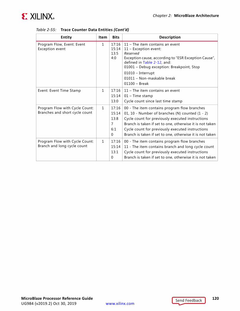
Chapter 2: MicroBlaze Architecture
Program Flow, Event: Event Exception event
1 17:1615:1413:5 4:0
11 – The item contains an event 11 – Exception event: Reserved Exception cause, according to “ESR Exception Cause”, defined in Table 2-12, and: 01001 – Debug exception: Breakpoint, Stop
01010 – Interrupt01011 – Non-maskable break01100 – Break
Event: Event Time Stamp 1 17:1615:1413:0
11 – The item contains an event01 – Time stampCycle count since last time stamp
Program Flow with Cycle Count: Branches and short cycle count
1 17:1615:1413:876:10
00 - The item contains program flow branches01, 10 - Number of branches (N) counted (1 - 2)Cycle count for previously executed instructionsBranch is taken if set to one, otherwise it is not takenCycle count for previously executed instructionsBranch is taken if set to one, otherwise it is not taken
Program Flow with Cycle Count: Branch and long cycle count
1 17:1615:1413:10
00 - The item contains program flow branches11 - The item contains branch and long cycle countCycle count for previously executed instructionsBranch is taken if set to one, otherwise it is not taken
Table 2-55: Trace Counter Data Entities (Cont’d)
Entity Item Bits Description
MicroBlaze Processor Reference Guide 120UG984 (v2019.2) Oct 30, 2019 www.xilinx.com
Send Feedback
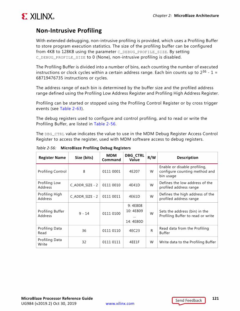
Chapter 2: MicroBlaze Architecture
Non-Intrusive ProfilingWith extended debugging, non-intrusive profiling is provided, which uses a Profiling Buffer to store program execution statistics. The size of the profiling buffer can be configured from 4KB to 128KB using the parameter C_DEBUG_PROFILE_SIZE. By setting C_DEBUG_PROFILE_SIZE to 0 (None), non-intrusive profiling is disabled.
The Profiling Buffer is divided into a number of bins, each counting the number of executed instructions or clock cycles within a certain address range. Each bin counts up to 236 - 1 = 68719476735 instructions or cycles.
The address range of each bin is determined by the buffer size and the profiled address range defined using the Profiling Low Address Register and Profiling High Address Register.
Profiling can be started or stopped using the Profiling Control Register or by cross trigger events (see Table 2-63).
The debug registers used to configure and control profiling, and to read or write the Profiling Buffer, are listed in Table 2-56.
The DBG_CTRL value indicates the value to use in the MDM Debug Register Access Control Register to access the register, used with MDM software access to debug registers.
Table 2-56: MicroBlaze Profiling Debug Registers
Register Name Size (bits) MDM Command
DBG_CTRL Value R/W Description
Profiling Control 8 0111 0001 4E207 WEnable or disable profiling, configure counting method and bin usage
Profiling Low Address C_ADDR_SIZE - 2 0111 0010 4E41D W Defines the low address of the
profiled address range
Profiling High Address C_ADDR_SIZE - 2 0111 0011 4E61D W Defines the high address of the
profiled address range
Profiling Buffer Address 9 - 14 0111 0100
9: 4E80810: 4E809
...14: 4E80D
W Sets the address (bin) in the Profiling Buffer to read or write
Profiling Data Read 36 0111 0110 4EC23 R Read data from the Profiling
Buffer
Profiling Data Write 32 0111 0111 4EE1F W Write data to the Profiling Buffer
MicroBlaze Processor Reference Guide 121UG984 (v2019.2) Oct 30, 2019 www.xilinx.com
Send Feedback
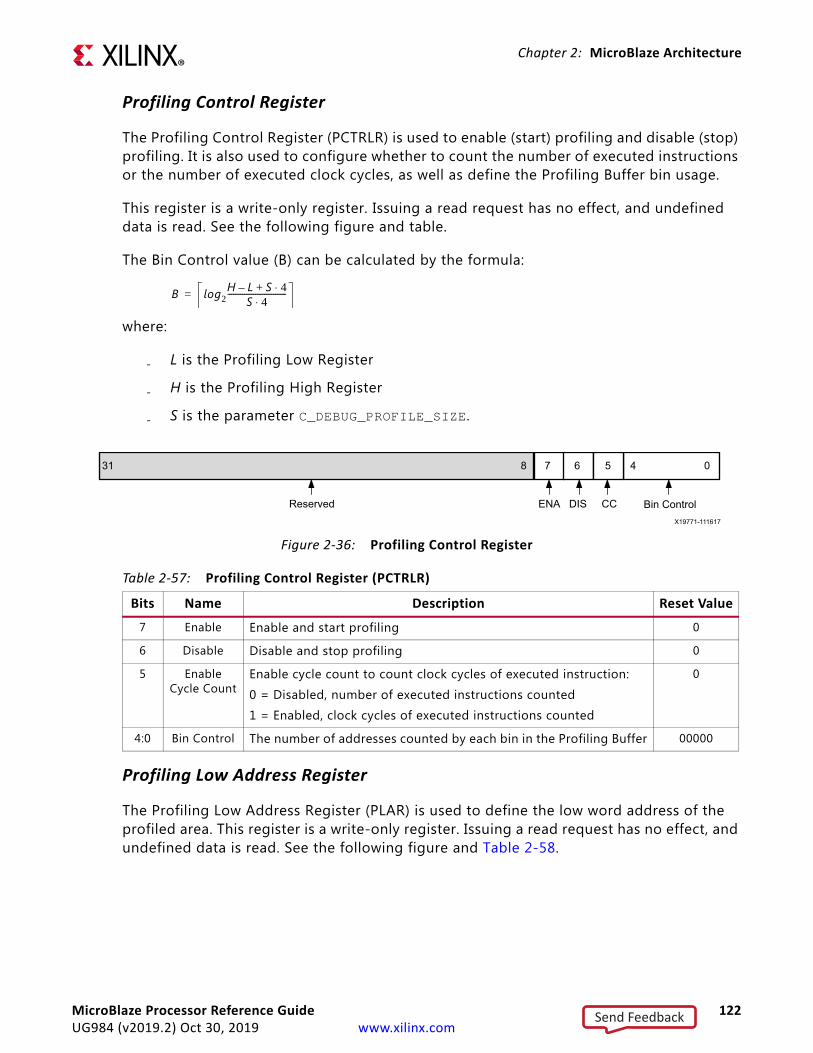
Chapter 2: MicroBlaze Architecture
Profiling Control Register
The Profiling Control Register (PCTRLR) is used to enable (start) profiling and disable (stop) profiling. It is also used to configure whether to count the number of executed instructions or the number of executed clock cycles, as well as define the Profiling Buffer bin usage.
This register is a write-only register. Issuing a read request has no effect, and undefined data is read. See the following figure and table.
The Bin Control value (B) can be calculated by the formula:
where:
- L is the Profiling Low Register
- H is the Profiling High Register
- S is the parameter C_DEBUG_PROFILE_SIZE.
Profiling Low Address Register
The Profiling Low Address Register (PLAR) is used to define the low word address of the profiled area. This register is a write-only register. Issuing a read request has no effect, and undefined data is read. See the following figure and Table 2-58.
B log2H L– S 4⋅+
S 4⋅--------------------------------=
X-Ref Target - Figure 2-36
Figure 2-36: Profiling Control Register
08
Reserved
31 7 6 5
Bin ControlCCDISENA
4
X19771-111617
Table 2-57: Profiling Control Register (PCTRLR)
Bits Name Description Reset Value
7 Enable Enable and start profiling 0
6 Disable Disable and stop profiling 0
5 Enable Cycle Count
Enable cycle count to count clock cycles of executed instruction:
0 = Disabled, number of executed instructions counted
1 = Enabled, clock cycles of executed instructions counted
0
4:0 Bin Control The number of addresses counted by each bin in the Profiling Buffer 00000
MicroBlaze Processor Reference Guide 122UG984 (v2019.2) Oct 30, 2019 www.xilinx.com
Send Feedback
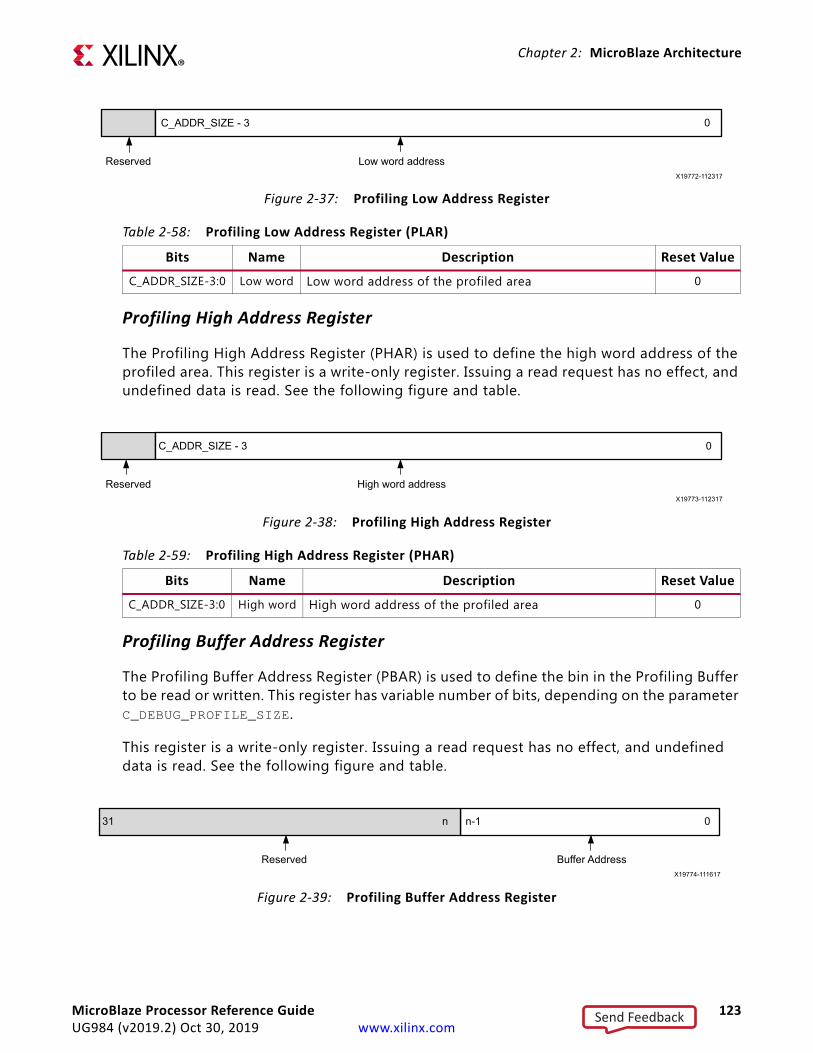
Chapter 2: MicroBlaze Architecture
Profiling High Address Register
The Profiling High Address Register (PHAR) is used to define the high word address of the profiled area. This register is a write-only register. Issuing a read request has no effect, and undefined data is read. See the following figure and table.
Profiling Buffer Address Register
The Profiling Buffer Address Register (PBAR) is used to define the bin in the Profiling Buffer to be read or written. This register has variable number of bits, depending on the parameter C_DEBUG_PROFILE_SIZE.
This register is a write-only register. Issuing a read request has no effect, and undefined data is read. See the following figure and table.
X-Ref Target - Figure 2-37
Figure 2-37: Profiling Low Address Register
0
Low word address
C_ADDR_SIZE - 3
ReservedX19772-112317
Table 2-58: Profiling Low Address Register (PLAR)
Bits Name Description Reset Value
C_ADDR_SIZE-3:0 Low word Low word address of the profiled area 0
X-Ref Target - Figure 2-38
Figure 2-38: Profiling High Address Register
0
High word address
C_ADDR_SIZE - 3
ReservedX19773-112317
Table 2-59: Profiling High Address Register (PHAR)
Bits Name Description Reset Value
C_ADDR_SIZE-3:0 High word High word address of the profiled area 0
X-Ref Target - Figure 2-39
Figure 2-39: Profiling Buffer Address Register
0
Buffer Address
31 n
Reserved
n-1
X19774-111617
MicroBlaze Processor Reference Guide 123UG984 (v2019.2) Oct 30, 2019 www.xilinx.com
Send Feedback
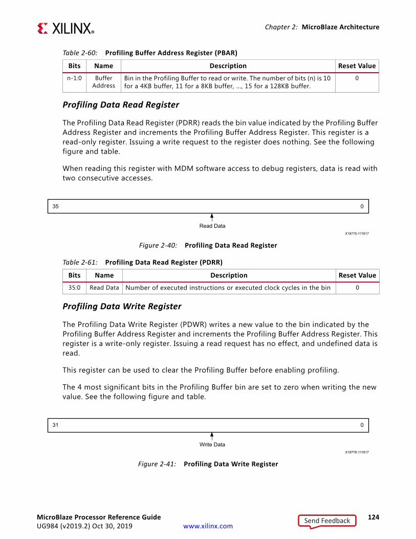
Chapter 2: MicroBlaze Architecture
Profiling Data Read Register
The Profiling Data Read Register (PDRR) reads the bin value indicated by the Profiling Buffer Address Register and increments the Profiling Buffer Address Register. This register is a read-only register. Issuing a write request to the register does nothing. See the following figure and table.
When reading this register with MDM software access to debug registers, data is read with two consecutive accesses.
Profiling Data Write Register
The Profiling Data Write Register (PDWR) writes a new value to the bin indicated by the Profiling Buffer Address Register and increments the Profiling Buffer Address Register. This register is a write-only register. Issuing a read request has no effect, and undefined data is read.
This register can be used to clear the Profiling Buffer before enabling profiling.
The 4 most significant bits in the Profiling Buffer bin are set to zero when writing the new value. See the following figure and table.
Table 2-60: Profiling Buffer Address Register (PBAR)
Bits Name Description Reset Value
n-1:0 Buffer Address
Bin in the Profiling Buffer to read or write. The number of bits (n) is 10 for a 4KB buffer, 11 for a 8KB buffer, …, 15 for a 128KB buffer.
0
X-Ref Target - Figure 2-40
Figure 2-40: Profiling Data Read Register
0
Read Data
35
X19775-111617
Table 2-61: Profiling Data Read Register (PDRR)
Bits Name Description Reset Value
35:0 Read Data Number of executed instructions or executed clock cycles in the bin 0
X-Ref Target - Figure 2-41
Figure 2-41: Profiling Data Write Register
0
Write Data
31
X19776-111617
MicroBlaze Processor Reference Guide 124UG984 (v2019.2) Oct 30, 2019 www.xilinx.com
Send Feedback
Chapter 2: MicroBlaze Architecture
Cross Trigger SupportWith basic debugging, cross trigger support is provided by two signals, DBG_STOP and MB_Halted.
• When the DBG_STOP input is set to 1, MicroBlaze will halt after a few instructions. XSDB will detect that MicroBlaze has halted, and indicate where the halt occurred. The signal can be used to halt MicroBlaze at any external event, for example when a Vivado® Integrated Logic Analyzer (ILA) is triggered.
• Whenever MicroBlaze is halted, the MB_Halted output signal is set to 1; for example after a breakpoint or watchpoint is hit, after a stop XSDB command, or when the DBG_STOP input is set. The output is cleared when MicroBlaze execution is resumed by an XSDB command.
The MB_Halted signal can be used to trigger a Vivado integrated logic analyzer, or halt other MicroBlaze cores in a multiprocessor system by connecting the signal to their DBG_STOP inputs.
With extended debugging, cross trigger support is available in conjunction with the MDM. The MDM provides programmable cross triggering between all connected processors, as well as external trigger inputs and outputs. For details, see the MicroBlaze Debug Module (MDM) Product Guide (PG115) [Ref 4].
MicroBlaze can handle up to eight cross trigger actions. Cross trigger actions are generated by the corresponding MDM cross trigger outputs, connected using the Debug bus. The effect of each of the cross trigger actions is listed in Table 2-63.
MicroBlaze can generate up to eight cross trigger events. Cross trigger events affect the corresponding MDM cross trigger inputs, connected using the Debug bus. The cross trigger events are described in Table 2-64.
Table 2-62: Profiling Data Write Register (PDWR)
Bits Name Description Reset Value
31:0 Write Data Data to write to a bin. 0
MicroBlaze Processor Reference Guide 125UG984 (v2019.2) Oct 30, 2019 www.xilinx.com
Send Feedback

Chapter 2: MicroBlaze Architecture
Table 2-63: MicroBlaze Cross Trigger Actions
Number Action Description
0 Debug stop Stop MicroBlaze if the processor is executing, and set the MB_Halted output. The same effect is achieved by setting the Dbg_Stop input.
1 Continue execution Continue execution if the processor is stopped, and clear the MB_Halted output.
2 Stop program trace Stop program trace if tracing is in progress.
3 Start program trace Start program trace if trace is stopped.
4 Stop performance monitoring
Stop performance monitoring if it is in progress.
5 Start performance monitoring
Start performance monitoring if it is stopped.
6 Disable profiling Disable profiling if it is in progress.
7 Enable profiling Enable profiling if it is disabled.
Table 2-64: MicroBlaze Cross Trigger Events
Number Event Description
0 MicroBlaze halted Generate an event when MicroBlaze is halted. The same event is signaled when the MB_Halted output is set.
1 Execution resumed Generate an event when the processor resumes execution from debug halt. The same event is signaled when the MB_Halted output is cleared.
2 Program trace stopped
Generate an event when program trace is stopped by writing a command to the Program Trace Command Register, when the trace buffer is full, or by a cross trigger action.
3 Program trace started
Generate an event when program trace is started by writing a command to the Program Trace Command Register, by hitting a tracepoint, or by a cross trigger action.
4 Performance monitoring stopped
Generate an event when performance monitoring is stopped by writing a command to the Performance Counter Command Register or by a cross trigger action.
5 Performance monitoring started
Generate an event when performance monitoring is started by writing a command to the Performance Counter Command Register, or by a cross trigger action.
6 Profiling disabled Generate an event when profiling is enabled by writing a command to the Profiling Control Register or by a cross trigger action.
7 Profiling enabled Generate an event when profiling is disabled by writing a command to the Profiling Control Register or by a cross trigger action.
MicroBlaze Processor Reference Guide 126UG984 (v2019.2) Oct 30, 2019 www.xilinx.com
Send Feedback
Chapter 2: MicroBlaze Architecture
Trace Interface OverviewThe MicroBlaze trace interface exports a number of internal state signals for performance monitoring and analysis.
RECOMMENDED: Xilinx recommends that users only use the trace interface through Xilinx developed analysis cores.
This interface is not guaranteed to be backward compatible in future releases of MicroBlaze. See Table 3-16 in Chapter 3, MicroBlaze Signal Interface Description for a list of exported signals.
MicroBlaze Processor Reference Guide 127UG984 (v2019.2) Oct 30, 2019 www.xilinx.com
Send Feedback

Chapter 2: MicroBlaze Architecture
Fault ToleranceThe fault tolerance features included in MicroBlaze, enabled with C_FAULT_TOLERANT, provide Error Detection for internal block RAMs (in the Instruction Cache, Data Cache, Branch Target Cache, and MMU), and support for Error Detection and Correction (ECC) in LMB block RAMs. When fault tolerance is enabled, all soft errors in block RAMs are detected and corrected, which significantly reduces overall failure intensity.
In addition to protecting block RAM, the FPGA configuration memory also generally needs to be protected. A detailed explanation of this topic, and further references, can be found in the two documents Soft Error Mitigation Controller LogiCORE IP Product Guide (PG036) [Ref 2] and UltraScale Architecture Soft Error Mitigation Controller LogiCORE IP Product Guide (PG187) [Ref 16].
To further increase fault tolerance, a complete triple modular redundancy (TMR) solution is provided for MicroBlaze, using additional cores to handle majority voting and fault detection. See the Triple Modular Redundancy (TMR) Subsystem Product Guide (PG268) [Ref 7] for a complete description and implementation details.
Configuration
Using MicroBlaze Configuration
You can enable Fault tolerance on the General page of the MicroBlaze configuration dialog box.
After enabling fault tolerance in MicroBlaze, ECC is automatically enabled in the connected LMB BRAM Interface Controllers by the tools, when the system is generated. This means that nothing else needs to be configured to enable fault tolerance and minimal ECC support.
It is possible (albeit not recommended) to manually override ECC support, leaving the LMB BRAM unprotected, by disabling C_ECC in the configuration dialogs of all connected LMB BRAM Interface Controllers.
In this case, the internal MicroBlaze block RAM protection is still enabled, since fault tolerance is enabled.
Using LMB BRAM Interface Controller Configuration
As an alternative to the method described above, it is also possible to enable ECC in the configuration dialogs of all connected LMB BRAM Interface Controllers.
MicroBlaze Processor Reference Guide 128UG984 (v2019.2) Oct 30, 2019 www.xilinx.com
Send Feedback

Chapter 2: MicroBlaze Architecture
In this case, fault tolerance is automatically enabled in MicroBlaze by the tools, when the system is generated. This means that nothing else needs to be configured to enable ECC support and MicroBlaze fault tolerance.
ECC must either be enabled or disabled in all Controllers, which is enforced by a DRC.
It is possible to manually override fault tolerance support in MicroBlaze, by explicitly disabling C_FAULT_TOLERANT in the MicroBlaze configuration dialog. This is not recommended, unless no block RAM is used in MicroBlaze, and there is no need to handle bus exceptions from uncorrectable ECC errors.
FeaturesAn overview of all MicroBlaze fault tolerance features is given here. Further details on each feature can be found in the following sections:
• Instruction Cache
• Data Cache
• UTLB Management
• Branch Target Cache
• Exception Causes
The LMB BRAM Interface Controller v4.0 or later provides the LMB ECC implementation. For details, including performance and resource utilization, see the LMB BRAM Interface Controller LogiCORE IP Product Guide (PG112) [Ref 3].
Instruction and Data Cache Protection
To protect the block RAM in the Instruction and Data Cache, parity is used. When a parity error is detected, the corresponding cache line is invalidated. This forces the cache to reload the correct value from external memory. Parity is checked whenever a cache hit occurs.
Note: This scheme only works for write-through, and thus write-back data cache is not available when fault tolerance is enabled. This is enforced by a DRC.
When new values are written to a block RAM in the cache, parity is also calculated and written. One parity bit is used for the tag, one parity bit for the instruction cache data, and one parity bit for each word in a data cache line.
In many cases, enabling fault tolerance does not increase the required number of cache block RAMs, since spare bits can be used for the parity. Any increase in resource utilization, in particular number of block RAMs, can easily be seen in the MicroBlaze configuration dialog, when enabling fault tolerance.
MicroBlaze Processor Reference Guide 129UG984 (v2019.2) Oct 30, 2019 www.xilinx.com
Send Feedback

Chapter 2: MicroBlaze Architecture
Memory Management Unit Protection
To protect the block RAM in the MMU Unified Translation Look-Aside Buffer (UTLB), parity is used. When a parity error is detected during an address translation, a TLB miss exception occurs, forcing software to reload the entry.
When a new TLB entry is written using the TLBHI and TLBLO registers, parity is calculated. One parity bit is used for each entry.
Parity is also checked when a UTLB entry is read using the TLBHI and TLBLO registers. When a parity error is detected in this case, the entry is marked invalid by clearing the valid bit.
Enabling fault tolerance does not increase the MMU block RAM size, since a spare bit is available for the parity.
Branch Target Cache Protection
To protect block RAM in the Branch Target Cache, parity is used. When a parity error is detected when looking up a branch target address, the address is ignored, forcing a normal branch.
When a new branch address is written to the Branch Target Cache, parity is calculated. One parity bit is used for each address.
Enabling fault tolerance does not increase the Branch Target Cache block RAM size, since a spare bit is available for the parity.
Exception Handling
With fault tolerance enabled, if an error occurs in LMB block RAM, the LMB BRAM Interface Controller generates error signals on the LMB interface.
If exceptions are enabled in the MicroBlaze processor by setting the EE bit in the Machine Status Register, the uncorrectable error signal either generates an instruction bus exception or a data bus exception, depending on the affected interface.
Should a bus exception occur when an exception is in progress, MicroBlaze is halted, and the external error signal MB_Error is set. This behavior ensures that it is impossible to execute an instruction corrupted by an uncorrectable error.
Software Support
Scrubbing
To ensure that bit errors are not accumulated in block RAMs, they must be periodically scrubbed.
MicroBlaze Processor Reference Guide 130UG984 (v2019.2) Oct 30, 2019 www.xilinx.com
Send Feedback

Chapter 2: MicroBlaze Architecture
The standalone BSP provides the function microblaze_scrub() to perform scrubbing of the entire LMB block RAM and all MicroBlaze internal block RAMs used in a particular configuration. This function is intended to be called periodically from a timer interrupt routine. One location of each block RAM is scrubbed every time it is called, using persistent data to track the current locations.
The following example code illustrates how this can be done.
#include "xparameters.h"#include "xtmrctr.h"#include "xintc.h"#include "mb_interface.h"
#define SCRUB_PERIOD ...
XIntc InterruptController; /* The Interrupt Controller instance */XTmrCtr TimerCounterInst;/* The Timer Counter instance */
void MicroBlazeScrubHandler(void *CallBackRef, u8 TmrCtrNumber){/* Perform other timer interrupt processing here */microblaze_scrub();
}
int main (void){int Status;
/* * Initialize the timer counter so that it's ready to use, * specify the device ID that is generated in xparameters.h */Status = XTmrCtr_Initialize(&TimerCounterInst, TMRCTR_DEVICE_ID);if (Status != XST_SUCCESS) {return XST_FAILURE;
}
/* * Connect the timer counter to the interrupt subsystem such that * interrupts can occur. */Status = XIntc_Initialize(&InterruptController, INTC_DEVICE_ID);if (Status != XST_SUCCESS) {return XST_FAILURE;
}
/* * Connect a device driver handler that will be called when an * interrupt for the device occurs, the device driver handler performs * the specific interrupt processing for the device */Status = XIntc_Connect(&InterruptController, TMRCTR_DEVICE_ID,
(XInterruptHandler)XTmrCtr_InterruptHandler,(void *) &TimerCounterInst);
if (Status != XST_SUCCESS) {return XST_FAILURE;
}
MicroBlaze Processor Reference Guide 131UG984 (v2019.2) Oct 30, 2019 www.xilinx.com
Send Feedback

Chapter 2: MicroBlaze Architecture
/* * Start the interrupt controller such that interrupts are enabled for * all devices that cause interrupts, specifying real mode so that the * timer counter can cause interrupts thru the interrupt controller. */Status = XIntc_Start(&InterruptController, XIN_REAL_MODE);if (Status != XST_SUCCESS) {return XST_FAILURE;
}
/* * Setup the handler for the timer counter that will be called from the * interrupt context when the timer expires, specify a pointer to the * timer counter driver instance as the callback reference so the * handler is able to access the instance data */XTmrCtr_SetHandler(&TimerCounterInst, MicroBlazeScrubHandler,
&TimerCounterInst);
/* * Enable the interrupt of the timer counter so interrupts will occur * and use auto reload mode such that the timer counter will reload * itself automatically and continue repeatedly, without this option * it would expire once only */XTmrCtr_SetOptions(&TimerCounterInst, TIMER_CNTR_0,
XTC_INT_MODE_OPTION | XTC_AUTO_RELOAD_OPTION);
/* * Set a reset value for the timer counter such that it will expire * earlier than letting it roll over from 0, the reset value is loaded * into the timer counter when it is started */XTmrCtr_SetResetValue(TmrCtrInstancePtr,TmrCtrNumber,SCRUB_PERIOD);
/* * Start the timer counter such that it's incrementing by default, * then wait for it to timeout a number of times */XTmrCtr_Start(&TimerCounterInst, TIMER_CNTR_0);
...}
See the section Scrubbing for further details on how scrubbing is implemented, including how to calculate the scrubbing rate.
BRAM Driver
The standalone BSP BRAM driver is used to access the ECC registers in the LMB BRAM Interface Controller, and also provides a comprehensive self test.
By implementing the Vitis Xilinx C Project "Peripheral Tests", a self-test example including the BRAM self test for each LMB BRAM Interface Controller in the system is generated. Depending on the ECC features enabled in the LMB BRAM Interface Controller, this code will
MicroBlaze Processor Reference Guide 132UG984 (v2019.2) Oct 30, 2019 www.xilinx.com
Send Feedback
Chapter 2: MicroBlaze Architecture
perform all possible tests of the ECC function. See the Vitis Unified Software Platform Documentation [Ref 9] for more information.
The self-test example can be found in the standalone BSP BRAM driver source code, typically in the subdirectory microblaze_0/libsrc/bram_v3_03_a/src/xbram_selftest.c.
Scrubbing
Scrubbing Methods
Scrubbing is performed using specific methods for the different block RAMs:
• Instruction and data caches: All lines in the caches are cyclically invalidated using the WIC and WDC instructions respectively. This forces the cache to reload the cache line from external memory.
• Memory Management Unit UTLB: All entries in the UTLB are cyclically invalidated by writing the TLBHI register with the valid bit cleared.
• Branch Target Cache: The entire BTC is invalided by doing a synchronizing branch, BRI 4.
• LMB block RAM: All addresses in the memory are cyclically read and written, thus correcting any single bit errors on each address.
It is also possible to add interrupts for correctable errors from the LMB BRAM Interface Controllers, and immediately scrub this address in the interrupt handler, although in most cases it only improves reliability slightly.
The failing address can be determined by reading the Correctable Error First Failing Address Register in each of the LMB BRAM Interface Controllers.
To be able to generate an interrupt C_ECC_STATUS_REGISTERS must be set to 1 in the connected LMB BRAM Interface Controllers, and to read the failing address C_CE_FAILING_REGISTERS must be set to 1.
Calculating Scrubbing Rate
The scrubbing rate depends on failure intensity and desired reliability.
The approximate equation to determine the LMB memory scrubbing rate is in our case given by
where PW is the probability of an uncorrectable error in a memory word, BER is the soft error rate for a single memory bit, and SR is the Scrubbing Rate.
The soft error rates affecting block RAM for each product family can be found in the Device Reliability Report User Guide (UG116) [Ref 5].
PW 7602BER
SR2------------
≈
MicroBlaze Processor Reference Guide 133UG984 (v2019.2) Oct 30, 2019 www.xilinx.com
Send Feedback
Chapter 2: MicroBlaze Architecture
Use CasesSeveral common use cases are described here. These use cases are derived from the Processor LMB BRAM Interface Controller LogiCORE IP Product Guide (PG112) [Ref 3].
Minimal
This system is obtained when enabling fault tolerance in MicroBlaze, without doing any other configuration.
The system is suitable when area constraints are high, and there is no need for testing of the ECC function, or analysis of error frequency and location. No ECC registers are implemented. Single bit errors are corrected by the ECC logic before being passed to MicroBlaze. Uncorrectable errors set an error signal, which generates an exception in MicroBlaze.
Small
This system should be used when it is necessary to monitor error frequency, but there is no need for testing of the ECC function. It is a minimal system with Correctable Error Counter Register added to monitor single bit error rates. If the error rate is too high, the scrubbing rate should be increased to minimize the risk of a single bit error becoming an uncorrectable double bit error. Parameters set are C_ECC = 1 and C_CE_COUNTER_WIDTH = 10.
Typical
This system represents a typical use case, where it is required to monitor error frequency, as well as generating an interrupt to immediately correct a single bit error through software. It does not provide support for testing of the ECC function.
It is a small system with Correctable Error First Failing registers and Status register added. A single bit error will latch the address for the access into the Correctable Error First Failing Address Register and set the CE_STATUS bit in the ECC Status Register. An interrupt will be generated triggering MicroBlaze to read the failing address and then perform a read followed by a write on the failing address. This will remove the single bit error from the BRAM, thus reducing the risk of the single bit error becoming a uncorrectable double bit error. Parameters set are:
- C_ECC = 1
- C_CE_COUNTER_WIDTH = 10
- C_ECC_STATUS_REGISTER = 1
- C_CE_FAILING_REGISTERS = 1
MicroBlaze Processor Reference Guide 134UG984 (v2019.2) Oct 30, 2019 www.xilinx.com
Send Feedback

Chapter 2: MicroBlaze Architecture
Full
This system uses all of the features provided by the LMB BRAM Interface Controller, to enable full error injection capability, as well as error monitoring and interrupt generation. It is a typical system with Uncorrectable Error First Failing registers and Fault Injection registers added. All features are switched on for full control of ECC functionality for system debug or systems with high fault tolerance requirements. Parameters set are:
- C_ECC = 1
- C_CE_COUNTER_WIDTH = 10
- C_ECC_STATUS_REGISTER = 1
- C_CE_FAILING_REGISTERS = 1
- C_UE_FAILING_REGISTERS = 1
- C_FAULT_INJECT = 1
MicroBlaze Processor Reference Guide 135UG984 (v2019.2) Oct 30, 2019 www.xilinx.com
Send Feedback

Chapter 2: MicroBlaze Architecture
Lockstep OperationMicroBlaze is able to operate in a lockstep configuration, where two or more identical MicroBlaze cores execute the same program. By comparing the outputs of the cores, any tampering attempts, transient faults or permanent hardware faults can be detected.
System ConfigurationThe parameter C_LOCKSTEP_SLAVE is set to one on all slave MicroBlaze cores in the system, except the master (or primary) core. The master core drives all the output signals, and handles the debug functionality. The port Lockstep_Master_Out on the master is connected to the port Lockstep_Slave_In on the slaves, in order to handle debugging.
The slave cores should not drive any output signals, only receive input signals. This must be ensured by only connecting signals to the input ports of the slaves. For buses this means that each individual input port must be explicitly connected.
The port Lockstep_Out on the master and slave cores provide all output signals for comparison. Unless an error occurs, individual signals from each of the cores are identical every clock cycle.
To ensure that lockstep operation works properly, all input signals to the cores must be synchronous. Input signals that could require external synchronization are Interrupt, Reset, Ext_Brk, and Ext_Nm_Brk.
Use CasesTwo common use cases are described here. In addition, lockstep operation provides the basis for implementing triple modular redundancy on MicroBlaze core level.
Tamper Protection
This application represents a high assurance use case, where it is required that the system is tamper-proof. A typically example is a cryptographic application.
The approach involves having two redundant MicroBlaze processors with dedicated local memory and redundant comparators, each in a protected area. The outputs from each processor feed two comparators and each processor receive copies of every input signal.
The redundant MicroBlaze processors are functionally identical and completely independent of each other, without any connecting signals. The only exception is debug logic and associated signals, because it is assumed that debugging is disabled before any productization and certification of the system.
MicroBlaze Processor Reference Guide 136UG984 (v2019.2) Oct 30, 2019 www.xilinx.com
Send Feedback
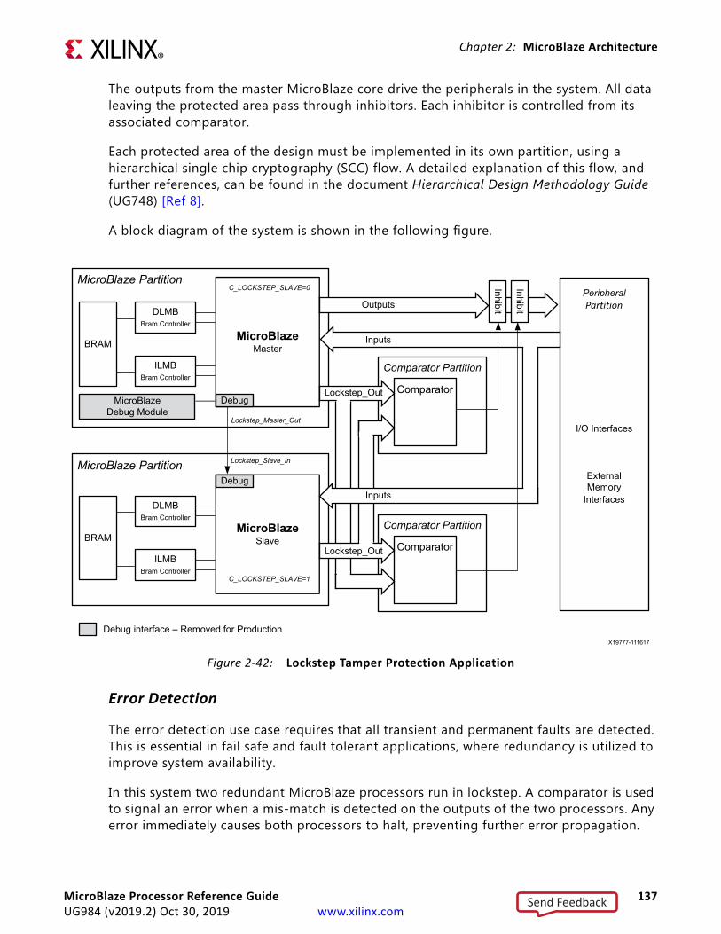
Chapter 2: MicroBlaze Architecture
The outputs from the master MicroBlaze core drive the peripherals in the system. All data leaving the protected area pass through inhibitors. Each inhibitor is controlled from its associated comparator.
Each protected area of the design must be implemented in its own partition, using a hierarchical single chip cryptography (SCC) flow. A detailed explanation of this flow, and further references, can be found in the document Hierarchical Design Methodology Guide (UG748) [Ref 8].
A block diagram of the system is shown in the following figure.
Error Detection
The error detection use case requires that all transient and permanent faults are detected. This is essential in fail safe and fault tolerant applications, where redundancy is utilized to improve system availability.
In this system two redundant MicroBlaze processors run in lockstep. A comparator is used to signal an error when a mis-match is detected on the outputs of the two processors. Any error immediately causes both processors to halt, preventing further error propagation.
X-Ref Target - Figure 2-42
Figure 2-42: Lockstep Tamper Protection Application
MicroBlaze Partition
BRAM
DLMBBram Controller
ILMBBram Controller
MicroBlaze Partition
BRAM
DLMBBram Controller
ILMBBram Controller
MicroBlazeMaster
DebugMicroBlazeDebug Module
MicroBlazeSlave
Debug
Comparator
I/O Interfaces
External Memory
Interfaces
Comparator Partition
Inputs
Comparator
Comparator Partition
Inhibit
PeripheralPartition
Inputs
Debug interface – Removed for Production
InhibitOutputs
C_LOCKSTEP_SLAVE=0
C_LOCKSTEP_SLAVE=1
Lockstep_Master_Out
Lockstep_Slave_In
Lockstep_Out
Lockstep_Out
X19777-111617
MicroBlaze Processor Reference Guide 137UG984 (v2019.2) Oct 30, 2019 www.xilinx.com
Send Feedback

Chapter 2: MicroBlaze Architecture
The redundant MicroBlaze processors are functionally identical, except for debug logic and associated signals.The outputs from the master MicroBlaze core drive the peripherals in the system. The slave MicroBlaze core only has inputs connected; all outputs are left open.
The system contains the basic building block for designing a complete fault tolerant application, where one or more additional blocks must be added to provide redundancy.
This use case is illustrated in the following figure.
X-Ref Target - Figure 2-43
Figure 2-43: Lockstep Error Detection Application
BRAM
DLMBBram Controller
ILMBBram Controller
MicroBlazeMaster
DebugMicroBlazeDebug Module
MicroBlazeSlave
Debug
Comparator
I/O Interfaces
External Memory
Interfaces
Error Reset
Inputs
C_LOCKSTEP_SLAVE=0
C_LOCKSTEP_SLAVE=1
Lockstep_Out
Lockstep_Out
Outputs
Inputs
Inputs
X19778-111617
MicroBlaze Processor Reference Guide 138UG984 (v2019.2) Oct 30, 2019 www.xilinx.com
Send Feedback

Chapter 2: MicroBlaze Architecture
CoherencyMicroBlaze supports cache coherency, as well as invalidation of caches and translation look-aside buffers, using the AXI Coherency Extension (ACE) defined in AMBA® AXI and ACE Protocol Specification (Arm IHI 0022E) [Ref 15]. The coherency support is enabled when the parameter C_INTERCONNECT is set to 3 (ACE).
Using ACE ensures coherency between the caches of all MicroBlaze processors in the coherency domain. The peripheral ports (AXI_IP, AXI_DP) and local memory (ILMB, DLMB) are outside the coherency domain.
Coherency is not supported with write-back data cache, wide cache interfaces (more than 32-bit data), instruction cache streams, instruction cache victims or when area optimization is enabled. In addition both C_ICACHE_ALWAYS_USED and C_DCACHE_ALWAYS_USED must be set to 1.
InvalidationThe coherency hardware handles invalidation in the following cases:
• Data Cache invalidation: When a MicroBlaze core in the coherency domain invalidates a data cache line with an external cache invalidation instruction (WDC.EXT.CLEAR or WDC.EXT.FLUSH), hardware messages ensure that all other cores in the coherency domain will do the same. The physical address is always used.
• Instruction Cache invalidation: When a MicroBlaze core in the coherency domain invalidates an instruction cache line, hardware messages ensure that all other cores in the coherency domain will do the same. When the MMU is in virtual mode the virtual address is used, otherwise the physical address is used.
• MMU TLB invalidation: When a MicroBlaze core in the coherency domain invalidates an entry in the UTLB (that is writes TLBHI with a zero Valid flag), hardware messages ensure that all other cores in the coherency domain will invalidate all entries in their unified TLBs having a TAG matching the invalidated virtual address, as well as empty their shadow TLBs.
The TID is not taken into account when matching the entries, which can result in invalidation of entries belonging to other processes. Subsequent accesses to these entries will generate TLB miss exceptions, which must be handled by software.
Before invalidating an MMU page, it must first be loaded into the UTLB to ensure that the hardware invalidation is propagated within the coherency domain. It is not sufficient to simply invalidate the page in memory, since other processors in the coherency domain can have this particular entry stored in their TLBs.
MicroBlaze Processor Reference Guide 139UG984 (v2019.2) Oct 30, 2019 www.xilinx.com
Send Feedback

Chapter 2: MicroBlaze Architecture
After a MicroBlaze core has invalidated one or more entries, it must execute a memory barrier instruction (MBAR), to ensure that all peer processors have completed their TLB invalidation.
• Branch Target Cache invalidation: When a MicroBlaze core in the coherency domain invalidates the Branch Target Cache, either with a memory barrier instruction or with a synchronizing branch, hardware messages ensure that all other cores in the coherency domain will do the same.
In particular, this means that self-modifying code can be used transparently within the coherency domain in a multi-processor system, provided that the guidelines in Self-modifying Code are followed.
Protocol ComplianceThe MicroBlaze instruction cache interface issues the following subset of the possible ACE transactions:
• ReadClean: Issued when a cache line is allocated.
• ReadOnce: Issued when the cache is off, or if the MMU Inhibit Caching bit is set for the cache line.
The MicroBlaze data cache interface issues the following subset of the possible ACE transactions:
• ReadClean: Issued when a cache line is allocated.
• CleanUnique: Issued when an SWX instruction is executed as part of an exclusive access sequence.
• ReadOnce: Issued when the cache is off, or if the MMU Inhibit Caching bit is set for the cache line.
• WriteUnique: Issued whenever a store instruction performs a write.
• CleanInvalid: Issued when a WDC.EXT.FLUSH instruction is executed.
• MakeInvalid: Issued when a WDC.EXT.CLEAR instruction is executed.
MicroBlaze Processor Reference Guide 140UG984 (v2019.2) Oct 30, 2019 www.xilinx.com
Send Feedback
Chapter 2: MicroBlaze Architecture
Both interfaces issue the following subset of the possible Distributed Virtual Memory (DVM) transactions:
• DVM Operation
- TLB Invalidate: Hypervisor TLB Invalidate by VA
- Branch Predictor Invalidate: L Branch Predictor Invalidate all
- Physical Instruction Cache Invalidate: Non-secure Physical Instruction Cache Invalidate by PA without Virtual Index
- Virtual Instruction Cache Invalidate: Hypervisor Invalidate by VA
• DVM Sync
- Synchronization
• DVM Complete
- In addition to the DVM transactions above, the interfaces only accept the CleanInvalid and MakeInvalid transactions. These transactions have no effect in the instruction cache, and invalidate the indicated data cache lines. If any other transactions are received, the behavior is undefined.
- Only a subset of AXI4 transactions are utilized by the interfaces, as described in Cache Interfaces.
MicroBlaze Processor Reference Guide 141UG984 (v2019.2) Oct 30, 2019 www.xilinx.com
Send Feedback

Chapter 2: MicroBlaze Architecture
Data and Instruction Address ExtensionMicroBlaze has the ability to address up to 16EB of data controlled by the parameter C_ADDR_SIZE, and with 32-bit MicroBlaze also supports a physical instruction address up to 16EB when the MMU Physical Address Extension (PAE) is enabled by setting C_USE_MMU = 3 (Virtual).
With 64-bit MicroBlaze both the virtual and physical address are extended according to the parameter C_ADDR_SIZE. This applies to both instruction and data address spaces, thus eliminating all limitations imposed by using 32-bit MicroBlaze listed here.
The parameter C_ADDR_SIZE can be set to the following values:
There are a number of software limitations with extended addressing when using 32-bit MicroBlaze:
• The GNU tools only generate ELF files with 32-bit addresses with 32-bit MicroBlaze, which means that program instruction and data memory must be located in the first 4GB of the address space. This is also the reason the instruction address space does not provide an extended address unless PAE is enabled.
With PAE enabled, the majority of the program instruction and data can be located at any physical address, but all software running in real mode must be located in the first 4GB of the address space. The MMU UTLB must also be initialized to set up the virtual to physical address translation by software running in real mode, before virtual mode is activated.
• Because all software drivers use address pointers that are 32-bit unsigned integers, it is not possible to access physical extended addresses above 4GB without modifying the driver code, and consequently all AXI peripherals should be located in the first 4GB of the address space.
With PAE enabled, AXI peripherals can be located at any physical address, provided that the virtual address remains in the first 4GB of the address space.
° NONE 4 * 10243 bytes 32-bit address, no extended address instructions or PAE
° 64GB 64 * 10243 bytes 36-bit address
° 1TB 10244 bytes 40-bit address
° 16TB 16 * 10244 bytes 44-bit address
° 256TB 256 * 10244 bytes 48-bit address
° 4PB 4 * 10245 bytes 52-bit address
° 16EB 16 * 10246 bytes 64-bit address
MicroBlaze Processor Reference Guide 142UG984 (v2019.2) Oct 30, 2019 www.xilinx.com
Send Feedback
Chapter 2: MicroBlaze Architecture
• The extended address is only treated as a physical address, and the MMU cannot be used to translate from an extended virtual address to a physical address.
This also means that without PAE support, Linux can only use the data address extension through a dedicated driver operating in real mode.
The extended address load and store instructions are privileged when the MMU is enabled, unless they are allowed by setting the parameter C_MMU_PRIVILEGED_INSTR appropriately. If allowed, the instructions bypass the MMU translation treating the extended address as a physical address.
• The GNU compiler does not handle 64-bit address pointers, which means that unless PAE is enabled the only way to access an extended address is using the specific extended addressing instructions, available as macros.
The following C code exemplifies how an extended address can be used to access data:
#include “xil_types.h” #include “mb_interface.h”
int main(){u64 Addr = 0x000000FF00000000LL; /* Extended address */u32 Word;u8 Byte;
Word = lwea(Addr); /* Load word from extended address */swea(Addr, Word); /* Store word to extended address */Byte = lbuea(Addr); /* Load byte from extended address */sbea(Addr, Byte); /* Store byte to extended address */
}
MicroBlaze Processor Reference Guide 143UG984 (v2019.2) Oct 30, 2019 www.xilinx.com
Send Feedback
Chapter 3
MicroBlaze Signal Interface Description
IntroductionThis chapter describes the types of signal interfaces that can be used to connect a MicroBlaze™ processor.
OverviewThe MicroBlaze core is organized as a Harvard architecture with separate bus interface units for data and instruction accesses. The following two memory interfaces are supported: Local Memory Bus (LMB), and the AMBA® AXI4 interface (AXI4) and ACE interface (ACE).
The LMB provides single-cycle access to on-chip dual-port block RAM. The AXI4 interfaces provide a connection to both on-chip and off-chip peripherals and memory. The ACE interfaces provide cache coherent connections to memory.
MicroBlaze also supports up to 16 AXI4-Stream interface ports, each with one master and one slave interface.
FeaturesMicroBlaze can be configured with the following bus interfaces:
• The AMBA AXI4 Interface for peripheral interfaces, and the AMBA AXI4 or AXI Coherency Extension (ACE) Interface for cache interfaces (see Arm® AMBA® AXI and ACE Protocol Specification, Arm IHI 0022E [Ref 15]).
• LMB provides a simple synchronous protocol for efficient block RAM transfers• AXI4-Stream provides a fast non-arbitrated streaming communication mechanism• Debug interface for use with the Microprocessor Debug Module (MDM) core• Trace interface for performance analysis
MicroBlaze Processor Reference Guide 144UG984 (v2019.2) Oct 30, 2019 www.xilinx.com
Send Feedback
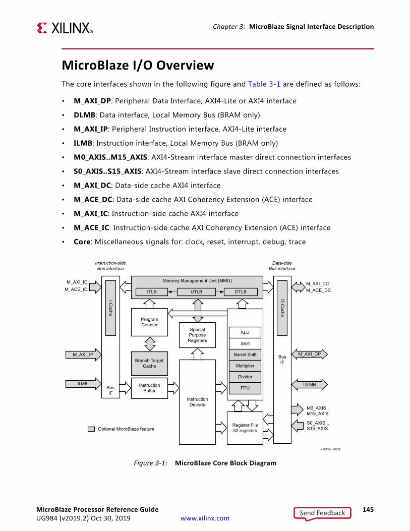
Chapter 3: MicroBlaze Signal Interface Description
MicroBlaze I/O OverviewThe core interfaces shown in the following figure and Table 3-1 are defined as follows:
• M_AXI_DP: Peripheral Data Interface, AXI4-Lite or AXI4 interface
• DLMB: Data interface, Local Memory Bus (BRAM only)
• M_AXI_IP: Peripheral Instruction interface, AXI4-Lite interface
• ILMB: Instruction interface, Local Memory Bus (BRAM only)
• M0_AXIS..M15_AXIS: AXI4-Stream interface master direct connection interfaces
• S0_AXIS..S15_AXIS: AXI4-Stream interface slave direct connection interfaces
• M_AXI_DC: Data-side cache AXI4 interface
• M_ACE_DC: Data-side cache AXI Coherency Extension (ACE) interface
• M_AXI_IC: Instruction-side cache AXI4 interface
• M_ACE_IC: Instruction-side cache AXI Coherency Extension (ACE) interface
• Core: Miscellaneous signals for: clock, reset, interrupt, debug, traceX-Ref Target - Figure 3-1
Figure 3-1: MicroBlaze Core Block Diagram
BusIF
I-Cache
Instruction Buffer
Instruction Buffer
Branch Target Cache
ProgramCounter
M_AXI_IC Memory Management Unit (MMU)
ITLB DTLBUTLB
BusIF
D-C
ache
M_AXI_DC
M_AXI_DP
DLMB
M0_AXIS .. M15_AXIS
S0_AXIS .. S15_AXIS
Special Purpose Registers
InstructionDecode
Register File32 registers
ALU
Shift
Barrel Shift
Multiplier
Divider
FPU
Instruction-sideBus interface
Data-sideBus interface
Optional MicroBlaze feature
M_AXI_IP
ILMB
M_ACE_DCM_ACE_IC
X19738-100218
MicroBlaze Processor Reference Guide 145UG984 (v2019.2) Oct 30, 2019 www.xilinx.com
Send Feedback

Chapter 3: MicroBlaze Signal Interface Description
Table 3-1: Summary of MicroBlaze Core I/O
Signal Interface I/O DescriptionM_AXI_DP_AWID M_AXI_DP O Master Write address ID
M_AXI_DP_AWADDR M_AXI_DP O Master Write address
M_AXI_DP_AWLEN M_AXI_DP O Master Burst length
M_AXI_DP_AWSIZE M_AXI_DP O Master Burst size
M_AXI_DP_AWBURST M_AXI_DP O Master Burst type
M_AXI_DP_AWLOCK M_AXI_DP O Master Lock type
M_AXI_DP_AWCACHE M_AXI_DP O Master Cache type
M_AXI_DP_AWPROT M_AXI_DP O Master Protection type
M_AXI_DP_AWQOS M_AXI_DP O Master Quality of Service
M_AXI_DP_AWVALID M_AXI_DP O Master Write address valid
M_AXI_DP_AWREADY M_AXI_DP I Slave Write address ready
M_AXI_DP_WDATA M_AXI_DP O Master Write data
M_AXI_DP_WSTRB M_AXI_DP O Master Write strobes
M_AXI_DP_WLAST M_AXI_DP O Master Write last
M_AXI_DP_WVALID M_AXI_DP O Master Write valid
M_AXI_DP_WREADY M_AXI_DP I Slave Write ready
M_AXI_DP_BID M_AXI_DP I Slave Response ID
M_AXI_DP_BRESP M_AXI_DP I Slave Write response
M_AXI_DP_BVALID M_AXI_DP I Slave Write response valid
M_AXI_DP_BREADY M_AXI_DP O Master Response ready
M_AXI_DP_ARID M_AXI_DP O Master Read address ID
M_AXI_DP_ARADDR M_AXI_DP O Master Read address
M_AXI_DP_ARLEN M_AXI_DP O Master Burst length
M_AXI_DP_ARSIZE M_AXI_DP O Master Burst size
M_AXI_DP_ARBURST M_AXI_DP O Master Burst type
M_AXI_DP_ARLOCK M_AXI_DP O Master Lock type
M_AXI_DP_ARCACHE M_AXI_DP O Master Cache type
M_AXI_DP_ARPROT M_AXI_DP O Master Protection type
M_AXI_DP_ARQOS M_AXI_DP O Master Quality of Service
M_AXI_DP_ARVALID M_AXI_DP O Master Read address valid
M_AXI_DP_ARREADY M_AXI_DP I Slave Read address ready
M_AXI_DP_RID M_AXI_DP I Slave Read ID tag
M_AXI_DP_RDATA M_AXI_DP I Slave Read data
M_AXI_DP_RRESP M_AXI_DP I Slave Read response
M_AXI_DP_RLAST M_AXI_DP I Slave Read last
MicroBlaze Processor Reference Guide 146UG984 (v2019.2) Oct 30, 2019 www.xilinx.com
Send Feedback
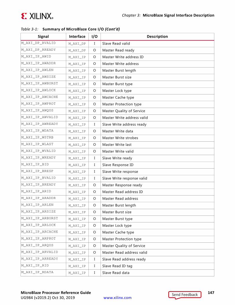
Chapter 3: MicroBlaze Signal Interface Description
M_AXI_DP_RVALID M_AXI_DP I Slave Read valid
M_AXI_DP_RREADY M_AXI_DP O Master Read ready
M_AXI_IP_AWID M_AXI_IP O Master Write address ID
M_AXI_IP_AWADDR M_AXI_IP O Master Write address
M_AXI_IP_AWLEN M_AXI_IP O Master Burst length
M_AXI_IP_AWSIZE M_AXI_IP O Master Burst size
M_AXI_IP_AWBURST M_AXI_IP O Master Burst type
M_AXI_IP_AWLOCK M_AXI_IP O Master Lock type
M_AXI_IP_AWCACHE M_AXI_IP O Master Cache type
M_AXI_IP_AWPROT M_AXI_IP O Master Protection type
M_AXI_IP_AWQOS M_AXI_IP O Master Quality of Service
M_AXI_IP_AWVALID M_AXI_IP O Master Write address valid
M_AXI_IP_AWREADY M_AXI_IP I Slave Write address ready
M_AXI_IP_WDATA M_AXI_IP O Master Write data
M_AXI_IP_WSTRB M_AXI_IP O Master Write strobes
M_AXI_IP_WLAST M_AXI_IP O Master Write last
M_AXI_IP_WVALID M_AXI_IP O Master Write valid
M_AXI_IP_WREADY M_AXI_IP I Slave Write ready
M_AXI_IP_BID M_AXI_IP I Slave Response ID
M_AXI_IP_BRESP M_AXI_IP I Slave Write response
M_AXI_IP_BVALID M_AXI_IP I Slave Write response valid
M_AXI_IP_BREADY M_AXI_IP O Master Response ready
M_AXI_IP_ARID M_AXI_IP O Master Read address ID
M_AXI_IP_ARADDR M_AXI_IP O Master Read address
M_AXI_IP_ARLEN M_AXI_IP O Master Burst length
M_AXI_IP_ARSIZE M_AXI_IP O Master Burst size
M_AXI_IP_ARBURST M_AXI_IP O Master Burst type
M_AXI_IP_ARLOCK M_AXI_IP O Master Lock type
M_AXI_IP_ARCACHE M_AXI_IP O Master Cache type
M_AXI_IP_ARPROT M_AXI_IP O Master Protection type
M_AXI_IP_ARQOS M_AXI_IP O Master Quality of Service
M_AXI_IP_ARVALID M_AXI_IP O Master Read address valid
M_AXI_IP_ARREADY M_AXI_IP I Slave Read address ready
M_AXI_IP_RID M_AXI_IP I Slave Read ID tag
M_AXI_IP_RDATA M_AXI_IP I Slave Read data
Table 3-1: Summary of MicroBlaze Core I/O (Cont’d)
Signal Interface I/O Description
MicroBlaze Processor Reference Guide 147UG984 (v2019.2) Oct 30, 2019 www.xilinx.com
Send Feedback

Chapter 3: MicroBlaze Signal Interface Description
M_AXI_IP_RRESP M_AXI_IP I Slave Read response
M_AXI_IP_RLAST M_AXI_IP I Slave Read last
M_AXI_IP_RVALID M_AXI_IP I Slave Read valid
M_AXI_IP_RREADY M_AXI_IP O Master Read ready
M_AXI_DC_AWADDR M_AXI_DC O Master Write address
M_AXI_DC_AWLEN M_AXI_DC O Master Burst length
M_AXI_DC_AWSIZE M_AXI_DC O Master Burst size
M_AXI_DC_AWBURST M_AXI_DC O Master Burst type
M_AXI_DC_AWLOCK M_AXI_DC O Master Lock type
M_AXI_DC_AWCACHE M_AXI_DC O Master Cache type
M_AXI_DC_AWPROT M_AXI_DC O Master Protection type
M_AXI_DC_AWQOS M_AXI_DC O Master Quality of Service
M_AXI_DC_AWVALID M_AXI_DC O Master Write address valid
M_AXI_DC_AWREADY M_AXI_DC I Slave Write address ready
M_AXI_DC_AWUSER M_AXI_DC O Master Write address user signals
M_AXI_DC_AWDOMAIN M_ACE_DC O Master Write address domain
M_AXI_DC_AWSNOOP M_ACE_DC O Master Write address snoop
M_AXI_DC_AWBAR M_ACE_DC O Master Write address barrier
M_AXI_DC_WDATA M_AXI_DC O Master Write data
M_AXI_DC_WSTRB M_AXI_DC O Master Write strobes
M_AXI_DC_WLAST M_AXI_DC O Master Write last
M_AXI_DC_WVALID M_AXI_DC O Master Write valid
M_AXI_DC_WREADY M_AXI_DC I Slave Write ready
M_AXI_DC_WUSER M_AXI_DC O Master Write user signals
M_AXI_DC_BRESP M_AXI_DC I Slave Write response
M_AXI_DC_BID M_AXI_DC I Slave Response ID
M_AXI_DC_BVALID M_AXI_DC I Slave Write response valid
M_AXI_DC_BREADY M_AXI_DC O Master Response ready
M_AXI_DC_BUSER M_AXI_DC I Slave Write response user signals
M_AXI_DC_WACK M_ACE_DC O Slave Write acknowledge
M_AXI_DC_ARID M_AXI_DC O Master Read address ID
M_AXI_DC_ARADDR M_AXI_DC O Master Read address
M_AXI_DC_ARLEN M_AXI_DC O Master Burst length
M_AXI_DC_ARSIZE M_AXI_DC O Master Burst size
M_AXI_DC_ARBURST M_AXI_DC O Master Burst type
Table 3-1: Summary of MicroBlaze Core I/O (Cont’d)
Signal Interface I/O Description
MicroBlaze Processor Reference Guide 148UG984 (v2019.2) Oct 30, 2019 www.xilinx.com
Send Feedback
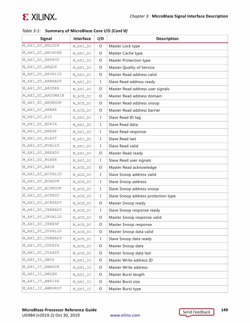
Chapter 3: MicroBlaze Signal Interface Description
M_AXI_DC_ARLOCK M_AXI_DC O Master Lock type
M_AXI_DC_ARCACHE M_AXI_DC O Master Cache type
M_AXI_DC_ARPROT M_AXI_DC O Master Protection type
M_AXI_DC_ARQOS M_AXI_DC O Master Quality of Service
M_AXI_DC_ARVALID M_AXI_DC O Master Read address valid
M_AXI_DC_ARREADY M_AXI_DC I Slave Read address ready
M_AXI_DC_ARUSER M_AXI_DC O Master Read address user signals
M_AXI_DC_ARDOMAIN M_ACE_DC O Master Read address domain
M_AXI_DC_ARSNOOP M_ACE_DC O Master Read address snoop
M_AXI_DC_ARBAR M_ACE_DC O Master Read address barrier
M_AXI_DC_RID M_AXI_DC I Slave Read ID tag
M_AXI_DC_RDATA M_AXI_DC I Slave Read data
M_AXI_DC_RRESP M_AXI_DC I Slave Read response
M_AXI_DC_RLAST M_AXI_DC I Slave Read last
M_AXI_DC_RVALID M_AXI_DC I Slave Read valid
M_AXI_DC_RREADY M_AXI_DC O Master Read ready
M_AXI_DC_RUSER M_AXI_DC I Slave Read user signals
M_AXI_DC_RACK M_ACE_DC O Master Read acknowledge
M_AXI_DC_ACVALID M_ACE_DC I Slave Snoop address valid
M_AXI_DC_ACADDR M_ACE_DC I Slave Snoop address
M_AXI_DC_ACSNOOP M_ACE_DC I Slave Snoop address snoop
M_AXI_DC_ACPROT M_ACE_DC I Slave Snoop address protection type
M_AXI_DC_ACREADY M_ACE_DC O Master Snoop ready
M_AXI_DC_CRREADY M_ACE_DC I Slave Snoop response ready
M_AXI_DC_CRVALID M_ACE_DC O Master Snoop response valid
M_AXI_DC_CRRESP M_ACE_DC O Master Snoop response
M_AXI_DC_CDVALID M_ACE_DC O Master Snoop data valid
M_AXI_DC_CDREADY M_ACE_DC I Slave Snoop data ready
M_AXI_DC_CDDATA M_ACE_DC O Master Snoop data
M_AXI_DC_CDLAST M_ACE_DC O Master Snoop data last
M_AXI_IC_AWID M_AXI_IC O Master Write address ID
M_AXI_IC_AWADDR M_AXI_IC O Master Write address
M_AXI_IC_AWLEN M_AXI_IC O Master Burst length
M_AXI_IC_AWSIZE M_AXI_IC O Master Burst size
M_AXI_IC_AWBURST M_AXI_IC O Master Burst type
Table 3-1: Summary of MicroBlaze Core I/O (Cont’d)
Signal Interface I/O Description
MicroBlaze Processor Reference Guide 149UG984 (v2019.2) Oct 30, 2019 www.xilinx.com
Send Feedback

Chapter 3: MicroBlaze Signal Interface Description
M_AXI_IC_AWLOCK M_AXI_IC O Master Lock type
M_AXI_IC_AWCACHE M_AXI_IC O Master Cache type
M_AXI_IC_AWPROT M_AXI_IC O Master Protection type
M_AXI_IC_AWQOS M_AXI_IC O Master Quality of Service
M_AXI_IC_AWVALID M_AXI_IC O Master Write address valid
M_AXI_IC_AWREADY M_AXI_IC I Slave Write address ready
M_AXI_IC_AWUSER M_AXI_IC O Master Write address user signals
M_AXI_IC_AWDOMAIN M_ACE_IC O Master Write address domain
M_AXI_IC_AWSNOOP M_ACE_IC O Master Write address snoop
M_AXI_IC_AWBAR M_ACE_IC O Master Write address barrier
M_AXI_IC_WDATA M_AXI_IC O Master Write data
M_AXI_IC_WSTRB M_AXI_IC O Master Write strobes
M_AXI_IC_WLAST M_AXI_IC O Master Write last
M_AXI_IC_WVALID M_AXI_IC O Master Write valid
M_AXI_IC_WREADY M_AXI_IC I Slave Write ready
M_AXI_IC_WUSER M_AXI_IC O Master Write user signals
M_AXI_IC_BID M_AXI_IC I Slave Response ID
M_AXI_IC_BRESP M_AXI_IC I Slave Write response
M_AXI_IC_BVALID M_AXI_IC I Slave Write response valid
M_AXI_IC_BREADY M_AXI_IC O Master Response ready
M_AXI_IC_BUSER M_AXI_IC I Slave Write response user signals
M_AXI_IC_WACK M_ACE_IC O Slave Write acknowledge
M_AXI_IC_ARID M_AXI_IC O Master Read address ID
M_AXI_IC_ARADDR M_AXI_IC O Master Read address
M_AXI_IC_ARLEN M_AXI_IC O Master Burst length
M_AXI_IC_ARSIZE M_AXI_IC O Master Burst size
M_AXI_IC_ARBURST M_AXI_IC O Master Burst type
M_AXI_IC_ARLOCK M_AXI_IC O Master Lock type
M_AXI_IC_ARCACHE M_AXI_IC O Master Cache type
M_AXI_IC_ARPROT M_AXI_IC O Master Protection type
M_AXI_IC_ARQOS M_AXI_IC O Master Quality of Service
M_AXI_IC_ARVALID M_AXI_IC O Master Read address valid
M_AXI_IC_ARREADY M_AXI_IC I Slave Read address ready
M_AXI_IC_ARUSER M_AXI_IC O Master Read address user signals
M_AXI_IC_ARDOMAIN M_ACE_IC O Master Read address domain
Table 3-1: Summary of MicroBlaze Core I/O (Cont’d)
Signal Interface I/O Description
MicroBlaze Processor Reference Guide 150UG984 (v2019.2) Oct 30, 2019 www.xilinx.com
Send Feedback

Chapter 3: MicroBlaze Signal Interface Description
M_AXI_IC_ARSNOOP M_ACE_IC O Master Read address snoop
M_AXI_IC_ARBAR M_ACE_IC O Master Read address barrier
M_AXI_IC_RID M_AXI_IC I Slave Read ID tag
M_AXI_IC_RDATA M_AXI_IC I Slave Read data
M_AXI_IC_RRESP M_AXI_IC I Slave Read response
M_AXI_IC_RLAST M_AXI_IC I Slave Read last
M_AXI_IC_RVALID M_AXI_IC I Slave Read valid
M_AXI_IC_RREADY M_AXI_IC O Master Read ready
M_AXI_IC_RUSER M_AXI_IC I Slave Read user signals
M_AXI_IC_RACK M_ACE_IC O Master Read acknowledge
M_AXI_IC_ACVALID M_ACE_IC I Slave Snoop address valid
M_AXI_IC_ACADDR M_ACE_IC I Slave Snoop address
M_AXI_IC_ACSNOOP M_ACE_IC I Slave Snoop address snoop
M_AXI_IC_ACPROT M_ACE_IC I Slave Snoop address protection type
M_AXI_IC_ACREADY M_ACE_IC O Master Snoop ready
M_AXI_IC_CRREADY M_ACE_IC I Slave Snoop response ready
M_AXI_IC_CRVALID M_ACE_IC O Master Snoop response valid
M_AXI_IC_CRRESP M_ACE_IC O Master Snoop response
M_AXI_IC_CDVALID M_ACE_IC O Master Snoop data valid
M_AXI_IC_CDREADY M_ACE_IC I Slave Snoop data ready
M_AXI_IC_CDDATA M_ACE_IC O Master Snoop data
M_AXI_IC_CDLAST M_ACE_IC O Master Snoop data last
Data_Addr[0:N-1] DLMB O Data interface LMB address bus, N = 32 - 64
Byte_Enable[0:3] DLMB O Data interface LMB byte enables
Data_Write[0:31] DLMB O Data interface LMB write data bus
D_AS DLMB O Data interface LMB address strobe
Read_Strobe DLMB O Data interface LMB read strobe
Write_Strobe DLMB O Data interface LMB write strobe
Data_Read[0:31] DLMB I Data interface LMB read data bus
DReady DLMB I Data interface LMB data ready
DWait DLMB I Data interface LMB data wait
DCE DLMB I Data interface LMB correctable error
DUE DLMB I Data interface LMB uncorrectable error
Instr_Addr[0:N-1] ILMB O Instruction interface LMB address bus, N = 32 - 64
I_AS ILMB O Instruction interface LMB address strobe
Table 3-1: Summary of MicroBlaze Core I/O (Cont’d)
Signal Interface I/O Description
MicroBlaze Processor Reference Guide 151UG984 (v2019.2) Oct 30, 2019 www.xilinx.com
Send Feedback

Chapter 3: MicroBlaze Signal Interface Description
IFetch ILMB O Instruction interface LMB instruction fetch
Instr[0:31] ILMB I Instruction interface LMB read data bus
IReady ILMB I Instruction interface LMB data ready
IWait ILMB I Instruction interface LMB data wait
ICE ILMB I Instruction interface LMB correctable error
IUE ILMB I Instruction interface LMB uncorrectable error
Mn_AXIS_TLAST M0_AXIS..M15_AXIS
O Master interface output AXI4 channels write last
Mn_AXIS_TDATA M0_AXIS..M15_AXIS
O Master interface output AXI4 channels write data
Mn_AXIS_TVALID M0_AXIS..M15_AXIS
O Master interface output AXI4 channels write valid
Mn_AXIS_TREADY M0_AXIS..M15_AXIS
I Master interface input AXI4 channels write ready
Sn_AXIS_TLAST S0_AXIS..S15_AXIS
I Slave interface input AXI4 channels write last
Sn_AXIS_TDATA S0_AXIS..S15_AXIS
I Slave interface input AXI4 channels write data
Sn_AXIS_TVALID S0_AXIS..S15_AXIS
I Slave interface input AXI4 channels write valid
Sn_AXIS_TREADY S0_AXIS..S15_AXIS
O Slave interface output AXI4 channels write ready
Interrupt Core I Interrupt. The signal is synchronized to Clk if the parameter C_ASYNC_INTERRUPT is set.
Interrupt_Address1 Core I Interrupt vector address
Interrupt_Ack1 Core O Interrupt acknowledge
Reset Core I Core reset, active high. Must be asserted 1 Clk clock cycle, but it is recommended to keep it asserted for at least 16 clock cycles.
Reset_Mode[0:1]3 Core I Reset mode. Sampled when Reset is active. SeeTable 3-2 for details.
Clk Core I Clock2
Ext_BRK3 Core I Break signal from MDM
Ext_NM_BRK3 Core I Non-maskable break signal from MDM
MB_Halted3 Core O Pipeline is halted, either using the Debug Interface, by setting Dbg_Stop, or by setting Reset_Mode[0:1] to 10.
Dbg_Stop3 Core I Unconditionally force pipeline to halt as soon as possible. Rising-edge detected pulse that should be held for at least 1 Clk clock cycle. The signal only has any effect when C_DEBUG_ENABLED is greater than 0.
Table 3-1: Summary of MicroBlaze Core I/O (Cont’d)
Signal Interface I/O Description
MicroBlaze Processor Reference Guide 152UG984 (v2019.2) Oct 30, 2019 www.xilinx.com
Send Feedback

Chapter 3: MicroBlaze Signal Interface Description
Dbg_Intr3 Core O Debug interrupt output, set when a Performance Monitor counter overflows, available when C_DEBUG_ENABLED is set to 2 (Extended).
MB_Error3 Core O Pipeline is halted due to a missed exception, when C_FAULT_TOLERANT is set to 1.
Sleep3 Core O MicroBlaze is in sleep mode after executing a SLEEP instruction or by setting Reset_Mode[0:1] to 10, all external accesses are completed, and the pipeline is halted.
Hibernate3 Core O MicroBlaze is in sleep mode after executing a HIBERNATE instruction, all external accesses are completed, and the pipeline is halted.
Suspend3 Core O MicroBlaze is in sleep mode after executing a SUSPEND instruction, all external accesses are completed, and the pipeline is halted.
Wakeup[0:1]3 Core I Wake MicroBlaze from sleep mode when either or both bits are set to 1. Ignored if MicroBlaze is not in sleep mode. The signals are individually synchronized to Clk according to the parameter C_ASYNC_WAKEUP[0:1].
Dbg_Wakeup3 Core O Debug request that external logic should wake MicroBlaze from sleep mode with the Wakeup signal, to allow debug access. Synchronous to Dbg_Update.
Pause3 Core I When this signal is set MicroBlaze pipeline will be paused after completing all ongoing bus accesses, and the Pause_Ack signal will be set. When this signal is cleared again MicroBlaze will continue normal execution where it was paused.
Pause_Ack3 Core O MicroBlaze is in pause mode after the Pause input signal has been set.
Dbg_Continue3 Core O Debug request that external logic should clear the Pause signal, to allow debug access.
Non_Secure[0:3]3 Core I Determines whether AXI accesses are non-secure or secure. The default value is binary 0000, setting all interfaces to be secure.Bit 0 = M_AXI_DPBit 1 = M_AXI_IPBit 2 = M_AXI_DCBit 3 = M_AXI_IC
Lockstep_... Core IO Lockstep signals for high integrity applications. See Table 3-13 for details.
Dbg_... Core IO Debug signals from MDM. See Table 3-15 for details.
Trace_... Core O Trace signals for real time HW analysis. See Table 3-16 for details.1. Only used with C_USE_INTERRUPT = 2, for low-latency interrupt support.2. MicroBlaze is a synchronous design clocked with the Clk signal, except for serial hardware debug logic, which is clocked with
the Dbg_Clk signal. If serial hardware debug logic is not used, there is no minimum frequency limit for Clk. However, if serial hardware debug logic is used, there are signals transferred between the two clock regions. In this case Clk must have a higher frequency than Dbg_Clk.
3. Only visible when C_ENABLE_DISCRETE_PORTS = 1.
Table 3-1: Summary of MicroBlaze Core I/O (Cont’d)
Signal Interface I/O Description
MicroBlaze Processor Reference Guide 153UG984 (v2019.2) Oct 30, 2019 www.xilinx.com
Send Feedback

Chapter 3: MicroBlaze Signal Interface Description
In general, MicroBlaze signals are synchronous to the Clk input signal. However, there are some exceptions controlled by parameters as described in the following table.
Sleep and Pause FunctionalityThere are two distinct ways of halting MicroBlaze execution in a controlled manner:
• Software controlled by executing an MBAR instruction to enter sleep mode.
• Hardware controlled by setting the input signal Pause to pause the pipeline.
Software Controlled
When an MBAR instruction is executed to enter sleep mode and MicroBlaze has completed all external accesses, the pipeline is halted and either the Sleep, Hibernate, or Suspend output signal is set.
Table 3-2: Effect of Reset Mode Inputs
Reset_Mode[0:1] Description
00 MicroBlaze starts executing at the reset vector, defined by C_BASE_VECTORS. This is the nominal default behavior.
01 MicroBlaze immediately enters sleep mode without performing any bus access, just as if a SLEEP instruction had been executed. The Sleep output is set to 1. When any of the Wakeup[0:1] signals is set, MicroBlaze starts executing at the reset vector, defined by C_BASE_VECTORS.This functionality can be useful in a multiprocessor configuration, allowing secondary processors to be configured without LMB memory.
10 If C_DEBUG_ENABLED is 0, the behavior is the same as if Reset_Mode[0:1] = 00.
If C_DEBUG_ENABLED is greater than 0, MicroBlaze immediately enters debug halt without performing any bus access, and the MB_Halted output is set to 1. When execution is continued via the debug interface, MicroBlaze starts executing at the reset vector, defined by C_BASE_VECTORS.
11 Reserved
Table 3-3: Parameter Controlled Asynchronous Signals
Signal Parameter Default DescriptionInterrupt C_ASYNC_INTERRUPT Tool controlled Parameter set from connected signal
Reset C_NUM_SYNC_FF_CLK 2 Parameter can be manually set to 0 for synchronous reset
Wakeup[0:1] C_ASYNC_WAKEUP
C_NUM_SYNC_FF_CLK
Tool controlled2
Set from connected signalsCan be manually set to 0 to override tool
Dbg_Wakeup C_DEBUG_INTERFACE 0 (serial) 0: Clocked by Dbg_Update1: Clocked by DEBUG_ACLK, synchronous to Clk
MicroBlaze Processor Reference Guide 154UG984 (v2019.2) Oct 30, 2019 www.xilinx.com
Send Feedback
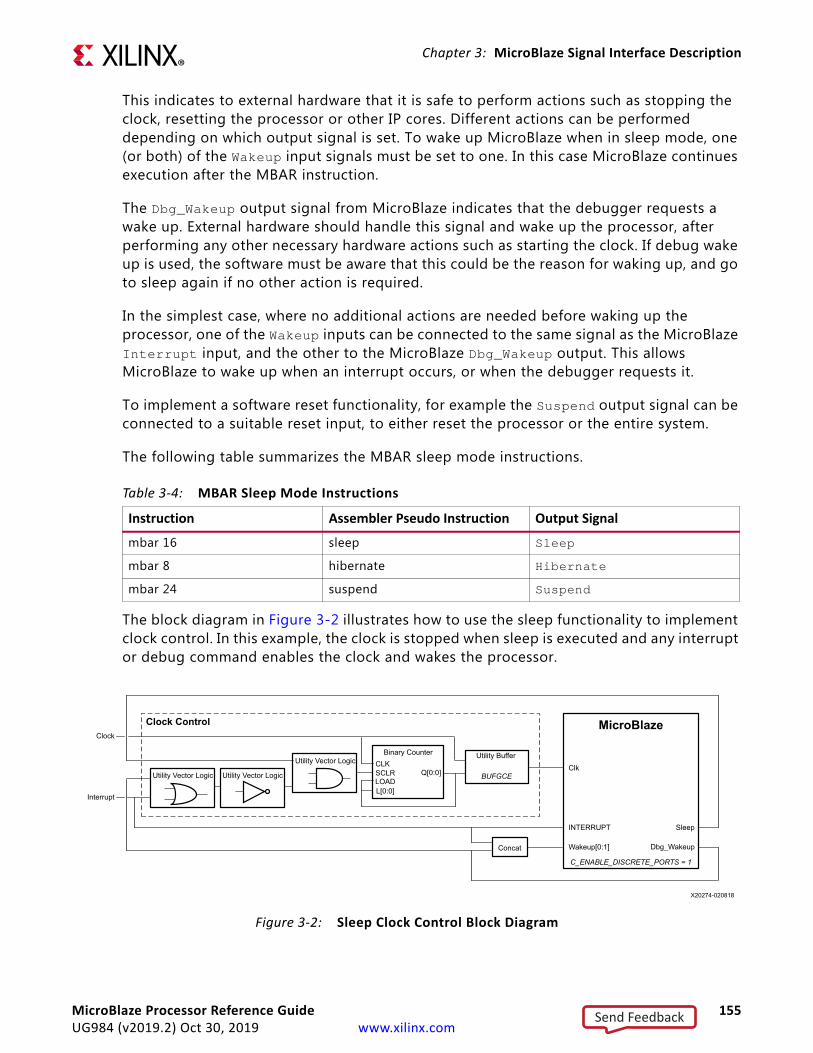
Chapter 3: MicroBlaze Signal Interface Description
This indicates to external hardware that it is safe to perform actions such as stopping the clock, resetting the processor or other IP cores. Different actions can be performed depending on which output signal is set. To wake up MicroBlaze when in sleep mode, one (or both) of the Wakeup input signals must be set to one. In this case MicroBlaze continues execution after the MBAR instruction.
The Dbg_Wakeup output signal from MicroBlaze indicates that the debugger requests a wake up. External hardware should handle this signal and wake up the processor, after performing any other necessary hardware actions such as starting the clock. If debug wake up is used, the software must be aware that this could be the reason for waking up, and go to sleep again if no other action is required.
In the simplest case, where no additional actions are needed before waking up the processor, one of the Wakeup inputs can be connected to the same signal as the MicroBlaze Interrupt input, and the other to the MicroBlaze Dbg_Wakeup output. This allows MicroBlaze to wake up when an interrupt occurs, or when the debugger requests it.
To implement a software reset functionality, for example the Suspend output signal can be connected to a suitable reset input, to either reset the processor or the entire system.
The following table summarizes the MBAR sleep mode instructions.
The block diagram in Figure 3-2 illustrates how to use the sleep functionality to implement clock control. In this example, the clock is stopped when sleep is executed and any interrupt or debug command enables the clock and wakes the processor.
Table 3-4: MBAR Sleep Mode Instructions
Instruction Assembler Pseudo Instruction Output Signal
mbar 16 sleep Sleep
mbar 8 hibernate Hibernate
mbar 24 suspend Suspend
X-Ref Target - Figure 3-2
Figure 3-2: Sleep Clock Control Block Diagram
MicroBlaze
C_ENABLE_DISCRETE_PORTS = 1
Utility Vector LogicBinary Counter
CLKSCLRLOADL[0:0]
Q[0:0]Utility Vector LogicUtility Vector Logic
Clock Control
Utility Buffer
BUFGCE
Sleep
Clk
Wakeup[0:1] Dbg_Wakeup
Interrupt
Clock
Concat
INTERRUPT
MicroBlaze Processor Reference Guide 155UG984 (v2019.2) Oct 30, 2019 www.xilinx.com
Send Feedback

Chapter 3: MicroBlaze Signal Interface Description
Instead of implementing the clock control with IP cores, an RTL Module can be used. A possible VHDL implementation corresponding to Clock Control in the block diagram in Figure 3-2 is given here. See the Vivado Design Suite User Guide: Designing IP Subsystems Using IP Integrator (UG994) [Ref 12] for more information on RTL Modules.
library IEEE;use IEEE.STD_LOGIC_1164.all;
library UNISIM;use UNISIM.VComponents.all;
entity clock_control is port ( clkin : in std_logic; reset : in std_logic; sleep : in std_logic; interrupt : in std_logic; dbg_wakeup : in std_logic; clkout : out std_logic );end clock_control;
architecture Behavioral of clock_control is attribute X_INTERFACE_INFO : string; attribute X_INTERFACE_INFO of clkin : signal is "xilinx.com:signal:clock:1.0 clk CLK"; attribute X_INTERFACE_INFO of reset : signal is "xilinx.com:signal:reset:1.0 reset RST"; attribute X_INTERFACE_INFO of interrupt : signal
is "xilinx.com:signal:interrupt:1.0 interrupt INTERRUPT"; attribute X_INTERFACE_INFO of clkout : signal is "xilinx.com:signal:clock:1.0 clk_out CLK";
attribute X_INTERFACE_PARAMETER : string; attribute X_INTERFACE_PARAMETER of reset : signal is "POLARITY ACTIVE_HIGH"; attribute X_INTERFACE_PARAMETER of interrupt : signal is "SENSITIVITY LEVEL_HIGH"; attribute X_INTERFACE_PARAMETER of clkout : signal is "FREQ_HZ 100000000";
signal clk_enable : std_logic := '1';begin
clock_enable_dff : process (clkin) is begin if clkin'event and clkin = '1' then if reset = '1' then clk_enable <= '1'; elsif sleep = '1' and interrupt = '0' and dbg_wakeup = '0' then clk_enable <= '0'; elsif clk_enable = '0' then clk_enable <= '1'; end if; end if; end process clock_enable_dff;
clock_enable : component BUFGCE port map ( O => clkout, CE => clk_enable, I => clkin );
end Behavioral;
MicroBlaze Processor Reference Guide 156UG984 (v2019.2) Oct 30, 2019 www.xilinx.com
Send Feedback

Chapter 3: MicroBlaze Signal Interface Description
Hardware Controlled
When the Pause input signal is set to one and MicroBlaze has completed all external accesses, the pipeline is halted and the Pause_Ack output signal is set. This indicates to external hardware that it is safe to perform actions such as stopping the clock, resetting the processor or other IP cores. To continue from pause, the input signal Pause must be cleared to zero. In this case MicroBlaze continues instruction execution where it was previously paused.
The Dbg_Continue output signal from MicroBlaze indicates that the debugger requests the processor to continue from pause. External hardware should handle this signal and clear pause after performing any other necessary hardware actions such as starting the clock.
After external hardware has set or cleared Pause, it is recommended to wait until Pause_Ack is set or cleared before Pause is changed again, to avoid any issues due to incorrectly detected pause acknowledge.
All signals used for hardware control (Pause, Pause_Ack, and Dbg_Continue) are synchronous to the MicroBlaze clock.
The block diagram in Figure 3-3 illustrates how to use the pause functionality to halt the processor and how to implement clock control. In this example, Pause is an external hardware signal that pauses processor execution and stops the clock. When Pause is cleared to zero, the clock is enabled and execution resumes. This example assumes that the external logic monitors Dbg_Continue, and clears Pause to allow debugging.
X-Ref Target - Figure 3-3
Figure 3-3: Pause Clock Control Block Diagram
MicroBlaze
C_ENABLE_DISCRETE_PORTS = 1
Utility Vector LogicBinary Counter
CLKSCLRLOADL[0:0]
Q[0:0]
Clock Control
Utility Buffer
BUFGCE
Pause_Ack
Clk
Pause
Dbg_Continue
Pause
Clock
Dbg_Continue
MicroBlaze Processor Reference Guide 157UG984 (v2019.2) Oct 30, 2019 www.xilinx.com
Send Feedback

Chapter 3: MicroBlaze Signal Interface Description
AXI4 and ACE Interface Description
Memory Mapped Interfaces
Peripheral Interfaces
The MicroBlaze AXI4 memory mapped peripheral interfaces are implemented as 32-bit masters. Each of these interfaces only have a single outstanding transaction at any time, and all transactions are completed in order.
• The instruction peripheral interface (M_AXI_IP) only performs single word read accesses, and is always set to use the AXI4-Lite subset.
• The data peripheral interface (M_AXI_DP) performs single word accesses, and is set to use the AXI4-Lite subset as default, but is set to use AXI4 when enabling exclusive access for LWX and SWX instructions. Halfword and byte writes are performed by setting the appropriate byte strobes.
The instruction peripheral interface (M_AXI_IP) address width can range from 32 - 64 bits when the MMU physical address extension (PAE) is enabled, depending on the value of the parameter C_ADDR_SIZE.
The data peripheral interface (M_AXI_DP) address width can range from 32 - 64 bits, depending on the value of the parameter C_ADDR_SIZE.
Cache Interfaces
The AXI4 memory mapped cache interfaces are implemented either as 32-bit, 128-bit, 256-bit, or 512-bit masters, depending on cache line length and data width parameters, whereas the AXI Coherency Extension (ACE) interfaces are implemented as 32-bit masters.
• With a 32-bit master, the instruction cache interface (M_AXI_IC or M_ACE_IC) performs 4 word, 8 word or 16 word burst read accesses, depending on cache line length. With 128-bit, 256-bit, or 512-bit masters, only single read accesses are performed.
With a 32-bit master, this interface can have multiple outstanding transactions, issuing up to 2 transactions or up to 5 transactions when stream cache is enabled. The stream cache can request two cache lines in advance, which means that in some cases 5 outstanding transactions can occur. In this case the number of outstanding reads is set to 8, since this must be a power of two. With 128-bit, 256-bit, or 512-bit masters, the interface only has a single outstanding transaction.
How memory locations are accessed depend on parameter C_ICACHE_ALWAYS_USED. If the parameter is 1, the cached memory range is always accessed using the AXI4 or ACE
MicroBlaze Processor Reference Guide 158UG984 (v2019.2) Oct 30, 2019 www.xilinx.com
Send Feedback
Chapter 3: MicroBlaze Signal Interface Description
cache interface. If the parameter is 0, the cached memory range is accessed over the AXI4 peripheral interface when the caches are software disabled (that is, MSR[ICE]=0).
• With a 32-bit master, the data cache interface (M_AXI_DC or M_ACE_DC) performs single word accesses, as well as 4 word, 8 word or 16 word burst accesses, depending on cache line length. Burst write accesses are only performed when using write-back cache with AXI4. With 128-bit, 256-bit, or 512-bit AXI4 masters, only single accesses are performed.
This interface can have multiple outstanding transactions, either issuing up to 2 transactions when reading, or up to 32 transactions when writing. MicroBlaze ensures that all outstanding writes are completed before a read is issued, since the processor must maintain an ordered memory model but AXI4 or ACE has separate read/write channels without any ordering. Using up to 32 outstanding write transactions improves performance, since it allows multiple writes to proceed without stalling the pipeline.
Word, halfword and byte writes are performed by setting the appropriate byte strobes.
Exclusive accesses can be enabled for LWX and SWX instructions.
How memory locations are accessed depend on the parameter C_DCACHE_ALWAYS_USED. If the parameter is 1, the cached memory range is always accessed using the AXI4 or ACE cache interface. If the parameter is 0, the cached memory range is accessed over the AXI4 peripheral interface when the caches are software disabled (that is, MSR[DCE]=0).
Interface Parameters and Signals
The relationship between MicroBlaze parameter settings and AXI4 interface behavior for tool-assigned parameters is summarized in the following table.
Table 3-5: AXI Memory Mapped Interface Parameters
Interface Parameter Description
M_AXI_DP C_M_AXI_DP_PROTOCOL AXI4-Lite: Default.AXI4: Used to allow exclusive access when C_M_AXI_DP_EXCLUSIVE_ACCESS is 1.
M_AXI_IC
M_ACE_IC
C_M_AXI_IC_DATA_WIDTH 32: Default, single word accesses and burst accesses with C_ICACHE_LINE_LEN word busts used with AXI4 and ACE.128: Used when C_ICACHE_DATA_WIDTH is set to 1 and C_ICACHE_LINE_LEN is set to 4 with AXI4. Only single accesses can occur.256: Used when C_ICACHE_DATA_WIDTH is set to 1 and C_ICACHE_LINE_LEN is set to 8 with AXI4. Only single accesses can occur.512: Used when C_ICACHE_DATA_WIDTH is set to 2, or when it is set to 1 and C_ICACHE_LINE_LEN is set to 16 with AXI4. Only single accesses can occur.
MicroBlaze Processor Reference Guide 159UG984 (v2019.2) Oct 30, 2019 www.xilinx.com
Send Feedback
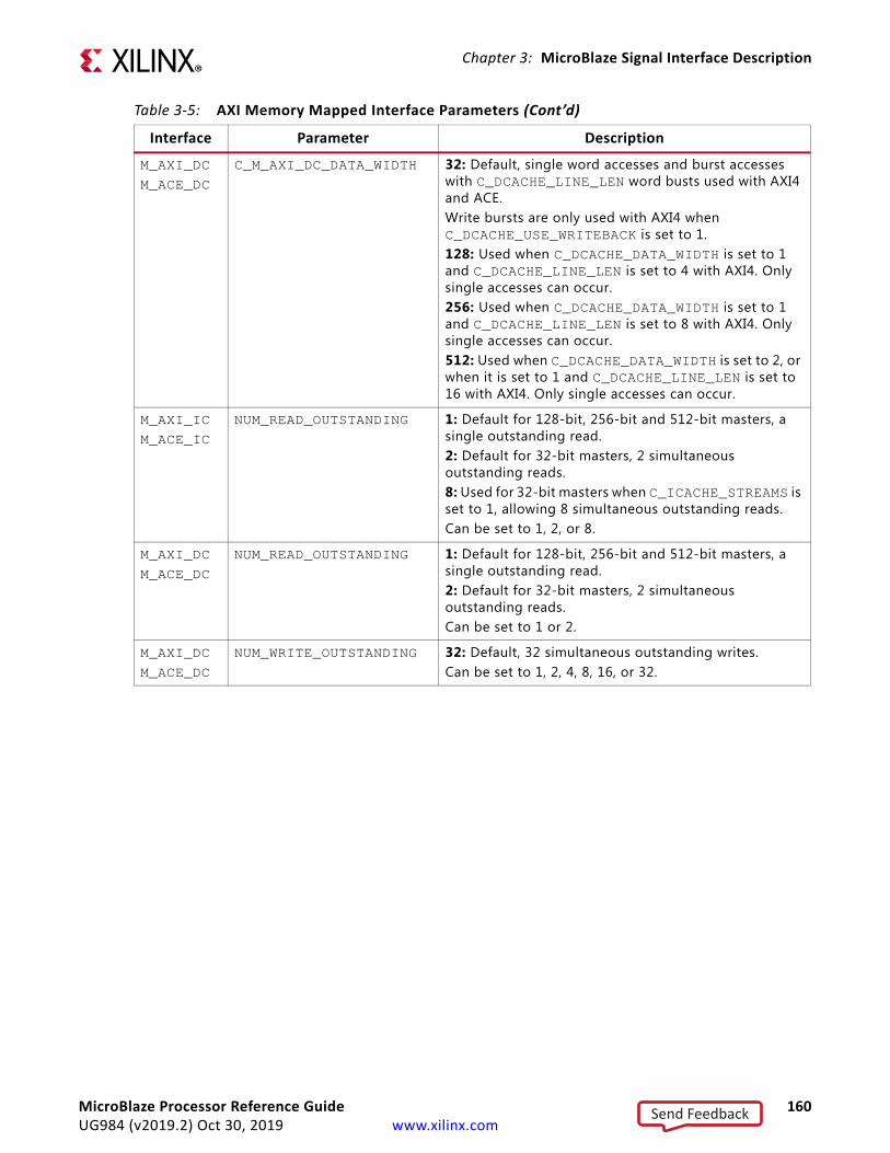
Chapter 3: MicroBlaze Signal Interface Description
M_AXI_DC
M_ACE_DC
C_M_AXI_DC_DATA_WIDTH 32: Default, single word accesses and burst accesses with C_DCACHE_LINE_LEN word busts used with AXI4 and ACE.Write bursts are only used with AXI4 when C_DCACHE_USE_WRITEBACK is set to 1.128: Used when C_DCACHE_DATA_WIDTH is set to 1 and C_DCACHE_LINE_LEN is set to 4 with AXI4. Only single accesses can occur.256: Used when C_DCACHE_DATA_WIDTH is set to 1 and C_DCACHE_LINE_LEN is set to 8 with AXI4. Only single accesses can occur.512: Used when C_DCACHE_DATA_WIDTH is set to 2, or when it is set to 1 and C_DCACHE_LINE_LEN is set to 16 with AXI4. Only single accesses can occur.
M_AXI_IC
M_ACE_IC
NUM_READ_OUTSTANDING 1: Default for 128-bit, 256-bit and 512-bit masters, a single outstanding read.2: Default for 32-bit masters, 2 simultaneous outstanding reads.8: Used for 32-bit masters when C_ICACHE_STREAMS is set to 1, allowing 8 simultaneous outstanding reads.Can be set to 1, 2, or 8.
M_AXI_DC
M_ACE_DC
NUM_READ_OUTSTANDING 1: Default for 128-bit, 256-bit and 512-bit masters, a single outstanding read.2: Default for 32-bit masters, 2 simultaneous outstanding reads.Can be set to 1 or 2.
M_AXI_DC
M_ACE_DC
NUM_WRITE_OUTSTANDING 32: Default, 32 simultaneous outstanding writes.Can be set to 1, 2, 4, 8, 16, or 32.
Table 3-5: AXI Memory Mapped Interface Parameters (Cont’d)
Interface Parameter Description
MicroBlaze Processor Reference Guide 160UG984 (v2019.2) Oct 30, 2019 www.xilinx.com
Send Feedback

Chapter 3: MicroBlaze Signal Interface Description
Values for access permissions, memory types, quality of service and shareability domain are defined in the following table.
Table 3-6: AXI Interface Signal Definitions
Interface Signal Description
M_AXI_IP C_M_AXI_IP_ARPROT Access Permission:• Unprivileged, secure instruction access (100) if input signal
Non_Secure[1] = 0• Unprivileged, non-secure instruction access (110) if input
signal Non_Secure[1] = 1
M_AXI_DP C_M_AXI_DP_ARCACHE
C_M_AXI_DP_AWCACHE
Memory Type, AXI4 protocol:• Normal Non-cacheable Bufferable (0011)
C_M_AXI_DP_ARPROT
C_M_AXI_DP_AWPROT
Access Permission, AXI4 and AXI4-Lite protocol:• Unprivileged, secure data access (000) if input signal
Non_Secure[0] = 0• Unprivileged, non-secure data access (010) if input signal
Non_Secure[0] = 1
C_M_AXI_DP_ARQOS
C_M_AXI_DP_AWQOS
Quality of Service, AXI4 protocol:• Priority 8 (1000)
M_AXI_IC C_M_AXI_IC_ARCACHE Memory Type:• Write-back Read and Write-allocate (1111)
M_ACE_IC C_M_AXI_IC_ARCACHE Memory Type, normal access:• Write-back Read and Write-allocate (1111)Memory Type, DVM access:• Normal Non-cacheable Non-bufferable (0010)
C_M_AXI_IC_ARDOMAIN Shareability Domain:• Inner shareable (01)
M_AXI_IC
M_ACE_IC
C_M_AXI_IC_ARPROT Access Permission:• Unprivileged, secure instruction access (100) if input signal
Non_Secure[3] = 0• Unprivileged, non-secure instruction access (110) if input
signal Non_Secure[3] = 1
C_M_AXI_IC_ARQOS Quality of Service:• Priority 7 (0111)
M_AXI_DC C_M_AXI_DC_ARCACHE Memory Type, normal access:• Write-back Read and Write-allocate (1111)Memory Type, exclusive access:• Normal Non-cacheable Non-bufferable (0010)
M_ACE_DC C_M_AXI_DC_ARCACHE Memory Type, normal and exclusive access:• Write-back Read and Write-allocate (1111)Memory Type, DVM access:• Normal Non-cacheable Non-bufferable (0010)
C_M_AXI_DC_ARDOMAIN
C_M_AXI_DC_AWDOMAIN
Shareability Domain:• Inner shareable (01)
MicroBlaze Processor Reference Guide 161UG984 (v2019.2) Oct 30, 2019 www.xilinx.com
Send Feedback

Chapter 3: MicroBlaze Signal Interface Description
The instruction cache interface (M_AXI_IC) address width can range from 32 - 64 bits when the MMU physical address extension (PAE) is enabled, depending on the value of the parameter C_ADDR_SIZE.
The data cache interface (M_AXI_DC or M_ACE_DC) address width can range from 32 - 64 bits, depending on the value of the parameter C_ADDR_SIZE.
See the AMBA AXI and ACE Protocol Specification (Arm IHI 0022E) [Ref 15] document for details.
Stream InterfacesThe MicroBlaze AXI4-Stream interfaces (M0_AXIS, M15_AXIS, S0_AXIS, S15_AXIS) are implemented as 32-bit masters and slaves. See the AMBA 4 AXI4-Stream Protocol Specification, Version 1.0 (Arm IHI 0051A) [Ref 14] document for further details.
Write Operation
A write to the stream interface is performed by MicroBlaze using one of the put or putd instructions. A write operation transfers the register contents to an output AXI4 interface. The transfer is completed in a single clock cycle for blocking mode writes (put and cput instructions) as long as the interface is not busy. If the interface is busy, the processor stalls until it becomes available. The non-blocking instructions (with prefix n), always complete in a single clock cycle even if the interface is busy. If the interface was busy, the write is inhibited and the carry bit is set in the MSR.
The control instructions (with prefix c) set the AXI4-Stream TLAST output, to ‘1’, which is used to indicate the boundary of a packet.
M_AXI_DC
M_ACE_DC
C_M_AXI_DC_AWCACHE Memory Type, normal access:• Write-back Read and Write-allocate (1111)Memory Type, exclusive access:• Normal Non-cacheable Non-bufferable (0010)
C_M_AXI_DC_ARPROT
C_M_AXI_DC_AWPROT
Access Permission:• Unprivileged, secure data access (000) if input signal
Non_Secure[2] = 0• Unprivileged, non-secure data access (010) if input signal
Non_Secure[2] = 1
C_M_AXI_DC_ARQOS Quality of Service, read access:• Priority 12 ((1100)
C_M_AXI_DC_AWQOS Quality of Service, write access:• Priority 8 (1000)
Table 3-6: AXI Interface Signal Definitions (Cont’d)
Interface Signal Description
MicroBlaze Processor Reference Guide 162UG984 (v2019.2) Oct 30, 2019 www.xilinx.com
Send Feedback
Chapter 3: MicroBlaze Signal Interface Description
Read Operation
A read from the stream interface is performed by MicroBlaze using one of the get or getd instructions. A read operations transfers the contents of an input AXI4 interface to a general purpose register. The transfer is typically completed in 2 clock cycles for blocking mode reads as long as data is available. If data is not available, the processor stalls at this instruction until it becomes available. In the non-blocking mode (instructions with prefix n), the transfer is completed in one or two clock cycles irrespective of whether or not data was available. In case data was not available, the transfer of data does not take place and the carry bit is set in the MSR.
The data get instructions (without prefix c) expect the AXI4-Stream TLAST input to be cleared to ‘0’, otherwise the instructions will set MSR[FSL] to ‘1’. Conversely, the control get instructions (with prefix c) expect the TLAST input to be set to ‘1’, otherwise the instructions will set MSR[FSL] to ‘1’. This can be used to check for the boundary of a packet.
MicroBlaze Processor Reference Guide 163UG984 (v2019.2) Oct 30, 2019 www.xilinx.com
Send Feedback

Chapter 3: MicroBlaze Signal Interface Description
Local Memory Bus (LMB) Interface DescriptionThe LMB is a synchronous bus used primarily to access on-chip block RAM. It uses a minimum number of control signals and a simple protocol to ensure that local block RAM are accessed in a single clock cycle. LMB signals and definitions are shown in the following table. All LMB signals are active high.
LMB Signal Interface
Addr[0:N-1]
The address bus is an output from the core and indicates the memory address that is being accessed by the current transfer. It is valid only when AS is high. In multicycle accesses requiring more than one clock cycle to complete), Addr[0:N-1] is valid only in the first clock cycle of the transfer.
Table 3-7: LMB Bus Signals
Signal Data Interface Instruction Interface Type Description
Addr[0:N-1]1
1. N = 32 - 64, set according to C_ADDR_SIZE, added in MicroBlaze v9.6.
Data_Addr[0:N-1]1 Instr_Addr[0:N-1]2
2. N = 32 - 64, set according to C_ADDR_SIZE when using PAE or 64-bit MicroBlaze, added in MicroBlaze v10.0.
O Address bus
Byte_Enable[0:3] Byte_Enable[0:3] not used O Byte enables
Data_Write[0:31] Data_Write[0:31] not used O Write data bus
AS D_AS I_AS O Address strobe
Read_Strobe Read_Strobe IFetch O Read in progress
Write_Strobe Write_Strobe not used O Write in progress
Data_Read[0:31] Data_Read[0:31] Instr[0:31] I Read data bus
Ready DReady IReady I Ready for next transfer
Wait3
3. Added in LMB for MicroBlaze v8.00
DWait IWait I Wait until accepted transfer is ready
CE3 DCE ICE I Correctable error
UE3 DUE IUE I Uncorrectable error
Clk Clk Clk I Bus clock
MicroBlaze Processor Reference Guide 164UG984 (v2019.2) Oct 30, 2019 www.xilinx.com
Send Feedback

Chapter 3: MicroBlaze Signal Interface Description
Byte_Enable[0:3]
The byte enable signals are outputs from the core and indicate which byte lanes of the data bus contain valid data. Byte_Enable[0:3]is valid only when AS is high. In multicycle accesses requiring more than one clock cycle to complete), Byte_Enable[0:3]is valid only in the first clock cycle of the transfer. Valid values for Byte_Enable[0:3]are shown in the following table:
Data_Write[0:31]
The write data bus is an output from the core and contains the data that is written to memory. It is valid only when AS is high. Only the byte lanes specified by Byte_Enable[0:3]contain valid data.
AS
The address strobe is an output from the core and indicates the start of a transfer and qualifies the address bus and the byte enables. It is high only in the first clock cycle of the transfer, after which it goes low and remains low until the start of the next transfer.
Read_Strobe
The read strobe is an output from the core and indicates that a read transfer is in progress. This signal goes high in the first clock cycle of the transfer, and can remain high until the clock cycle after Ready is sampled high. If a new read transfer is directly started in the next clock cycle, then Read_Strobe remains high.
Write_Strobe
The write strobe is an output from the core and indicates that a write transfer is in progress. This signal goes high in the first clock cycle of the transfer, and can remain high until the clock cycle after Ready is sampled high. If a new write transfer is directly started in the next clock cycle, then Write_Strobe remains high.
Table 3-8: Valid Values for Byte_Enable[0:3]
Byte_Enable[0:3]Byte Lanes Used
Data[0:7] Data[8:15] Data[16:23] Data[24:31]0001 •0010 •0100 •1000 •0011 • •1100 • •1111 • • • •
MicroBlaze Processor Reference Guide 165UG984 (v2019.2) Oct 30, 2019 www.xilinx.com
Send Feedback

Chapter 3: MicroBlaze Signal Interface Description
Data_Read[0:31]
The read data bus is an input to the core and contains data read from memory. Data_Read is valid on the rising edge of the clock when Ready is high.
Ready
The Ready signal is an input to the core and indicates completion of the current transfer and that the next transfer can begin in the following clock cycle. It is sampled on the rising edge of the clock. For reads, this signal indicates the Data_Read[0:31]bus is valid, and for writes it indicates that the Data_Write[0:31] bus has been written to local memory.
Wait
The Wait signal is an input to the core and indicates that the current transfer has been accepted, but not yet completed. It is sampled on the rising edge of the clock.
CE
The CE signal is an input to the core and indicates that the current transfer had a correctable error. It is valid on the rising edge of the clock when Ready is high. For reads, this signal indicates that an error has been corrected on the Data_Read[0:31] bus, and for byte and halfword writes it indicates that the corresponding data word in local memory has been corrected before writing the new data.
UE
The UE signal is an input to the core and indicates that the current transfer had an uncorrectable error. It is valid on the rising edge of the clock when Ready is high. For reads, this signal indicates that the value of the Data_Read[0:31]bus is erroneous, and for byte and halfword writes it indicates that the corresponding data word in local memory was erroneous before writing the new data.
Clk
All operations on the LMB are synchronous to the MicroBlaze core clock.
MicroBlaze Processor Reference Guide 166UG984 (v2019.2) Oct 30, 2019 www.xilinx.com
Send Feedback

Chapter 3: MicroBlaze Signal Interface Description
LMB TransactionsThe following diagrams provide examples of LMB bus operations.
Generic Write OperationsX-Ref Target - Figure 3-4
Figure 3-4: LMB Generic Write Operation, 0 Wait States
A0
BE0
D0
Don’t Care
Clk
Addr
Byte_Enable
Data_Write
AS
Read_Strobe
Wirte_Strobe
Data_Read
Ready
Wait
CE
UE
X-Ref Target - Figure 3-5
Figure 3-5: LMB Generic Write Operation, N Wait States
A0
BE0
D0
Don’t Care
Clk
Addr
Byte_Enable
Data_Write
AS
Read_Strobe
Wirte_Strobe
Data_Read
Ready
Wait
CE
UE
MicroBlaze Processor Reference Guide 167UG984 (v2019.2) Oct 30, 2019 www.xilinx.com
Send Feedback

Chapter 3: MicroBlaze Signal Interface Description
Generic Read OperationsX-Ref Target - Figure 3-6
Figure 3-6: LMB Generic Read Operation, 0 Wait States
A0
D0
Don’t Care
Clk
Addr
Byte_Enable
Data_Write
AS
Read_Strobe
Wirte_Strobe
Data_Read
Ready
Wait
CE
UE
X-Ref Target - Figure 3-7
Figure 3-7: LMB Generic Read Operation, N Wait States
A0
D0
Don’t Care
Clk
Addr
Byte_Enable
Data_Write
AS
Read_Strobe
Wirte_Strobe
Data_Read
Ready
Wait
CE
UE
MicroBlaze Processor Reference Guide 168UG984 (v2019.2) Oct 30, 2019 www.xilinx.com
Send Feedback

Chapter 3: MicroBlaze Signal Interface Description
Back-to-Back Write Operation
Back-to-Back Read Operation
X-Ref Target - Figure 3-8
Figure 3-8: LMB Back-to-Back Write Operation
A0
BE0
D0
A1
BE1
D1
A2
BE2
D2
A3
BE3
D3
A4
BE4
D4
Don’t Care Don’t Care Don’t Care
Clk
Addr
Byte_Enable
Data_Write
AS
Read_Strobe
Wirte_Strobe
Data_Read
Ready
Wait
CE
UE
X-Ref Target - Figure 3-9
Figure 3-9: LMB Back-to-Back Read Operation
A0 A1 A2 A3 A4
D0 D1 D2 D3 D4
Don’t Care Don’t Care Don’t Care
Clk
Addr
Byte_Enable
Data_Write
AS
Read_Strobe
Wirte_Strobe
Data_Read
Ready
Wait
CE
UE
MicroBlaze Processor Reference Guide 169UG984 (v2019.2) Oct 30, 2019 www.xilinx.com
Send Feedback
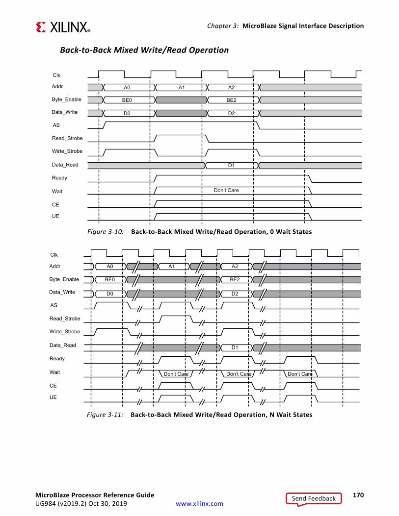
Chapter 3: MicroBlaze Signal Interface Description
Back-to-Back Mixed Write/Read OperationX-Ref Target - Figure 3-10
Figure 3-10: Back-to-Back Mixed Write/Read Operation, 0 Wait States
A0 A1 A2
BE0 BE2
D0 D2
D1
Don’t Care
Clk
Addr
Byte_Enable
Data_Write
AS
Read_Strobe
Wirte_Strobe
Data_Read
Ready
Wait
CE
UE
X-Ref Target - Figure 3-11
Figure 3-11: Back-to-Back Mixed Write/Read Operation, N Wait States
A0 A1 A2
BE0 BE2
D0 D2
D1
Don’t Care Don’t Care Don’t Care
Clk
Addr
Byte_Enable
Data_Write
AS
Read_Strobe
Wirte_Strobe
Data_Read
Ready
Wait
CE
UE
MicroBlaze Processor Reference Guide 170UG984 (v2019.2) Oct 30, 2019 www.xilinx.com
Send Feedback

Chapter 3: MicroBlaze Signal Interface Description
Read and Write Data SteeringThe MicroBlaze data-side bus interface performs the read steering and write steering required to support the following transfers:
• byte, halfword, and word transfers to word devices
• byte and halfword transfers to halfword devices
• byte transfers to byte devices
MicroBlaze does not support transfers that are larger than the addressed device. These types of transfers require dynamic bus sizing and conversion cycles that are not supported by the MicroBlaze bus interface. Data steering for read cycles are shown in Table 3-9 and Table 3-10, and data steering for write cycles are shown in Table 3-11 and Table 3-12.
Big endian format is only available when using the MMU in virtual or protected mode (C_USE_MMU > 1) or when reorder instructions are enabled (C_USE_REORDER_INSTR = 1).
Table 3-9: Big Endian Read Data Steering (Load to Register rD)
Address [LSB-1:LSB]
Byte_Enable[0:3] Transfer Size
Register rD Data
rD[0:7] rD[8:15] rD[16:23] rD[24:31]
11 0001 byte Byte3
10 0010 byte Byte2
01 0100 byte Byte1
00 1000 byte Byte0
10 0011 halfword Byte2 Byte3
00 1100 halfword Byte0 Byte1
00 1111 word Byte0 Byte1 Byte2 Byte3
Table 3-10: Little Endian Read Data Steering (Load to Register rD)
Address [LSB-1:LSB]
Byte_Enable[0:3] Transfer Size
Register rD Data
rD[0:7] rD[8:15] rD[16:23] rD[24:31]
11 1000 byte Byte0
10 0100 byte Byte1
01 0010 byte Byte2
00 0001 byte Byte3
10 1100 halfword Byte0 Byte1
00 0011 halfword Byte2 Byte3
00 1111 word Byte0 Byte1 Byte2 Byte3
MicroBlaze Processor Reference Guide 171UG984 (v2019.2) Oct 30, 2019 www.xilinx.com
Send Feedback

Chapter 3: MicroBlaze Signal Interface Description
Note: Other masters could have more restrictive requirements for byte lane placement than those allowed by MicroBlaze. Slave devices are typically attached “left-justified” with byte devices attached to the most-significant byte lane, and halfword devices attached to the most significant halfword lane. The MicroBlaze steering logic fully supports this attachment method.
Table 3-11: Big Endian Write Data Steering (Store from Register rD)
Address[LSB-1:LSB]
Byte_Enable[0:3] Transfer Size
Write Data Bus Bytes
Byte0 Byte1 Byte2 Byte3
11 0001 byte rD[24:31]
10 0010 byte rD[24:31]
01 0100 byte rD[24:31]
00 1000 byte rD[24:31]
10 0011 halfword rD[16:23] rD[24:31]
00 1100 halfword rD[16:23] rD[24:31]
00 1111 word rD[0:7] rD[8:15] rD[16:23] rD[24:31]
Table 3-12: Little Endian Write Data Steering (Store from Register rD)
Address[LSB-1:LSB]
Byte_Enable[0:3] Transfer Size
Write Data Bus Bytes
Byte3 Byte2 Byte1 Byte0
11 1000 byte rD[24:31]
10 0100 byte rD[24:31]
01 0010 byte rD[24:31]
00 0001 byte rD[24:31]
10 1100 halfword rD[16:23] rD[24:31]
00 0011 halfword rD[16:23] rD[24:31]
00 1111 word rD[0:7] rD[8:15] rD[16:23] rD[24:31]
MicroBlaze Processor Reference Guide 172UG984 (v2019.2) Oct 30, 2019 www.xilinx.com
Send Feedback
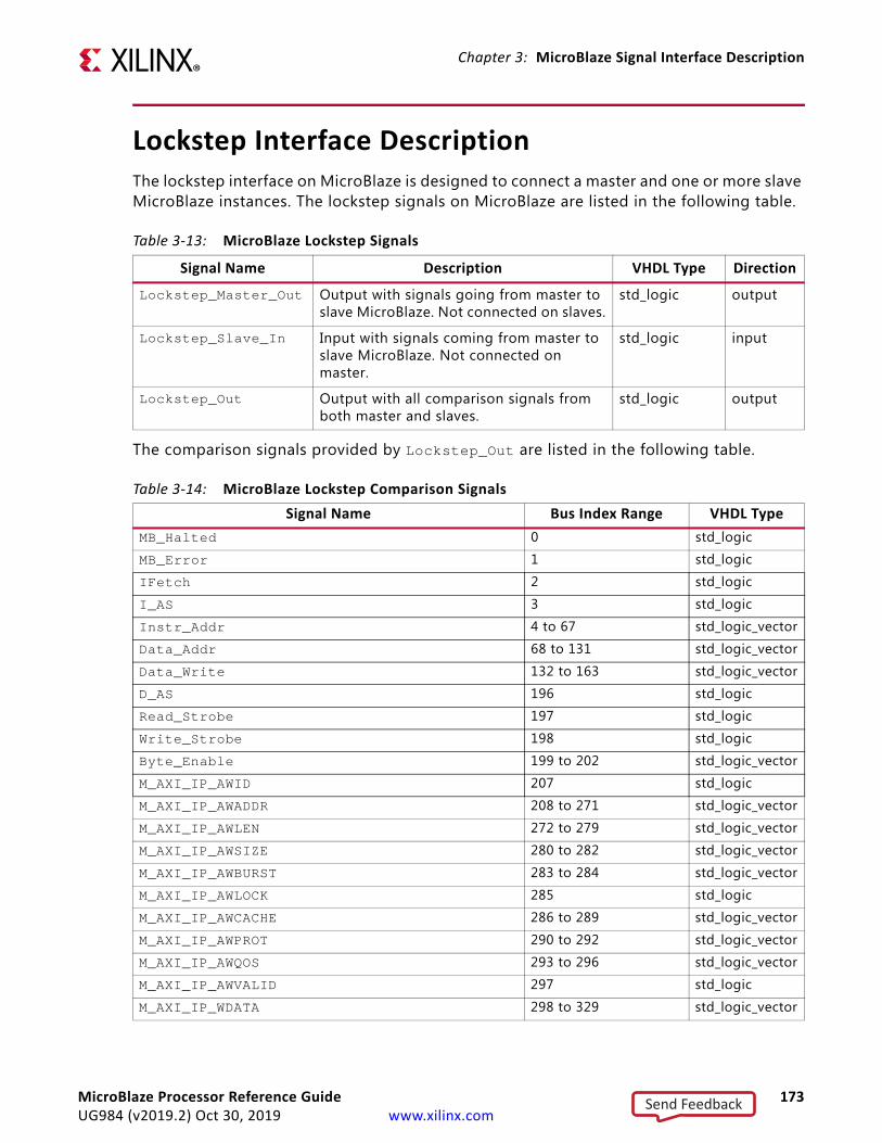
Chapter 3: MicroBlaze Signal Interface Description
Lockstep Interface DescriptionThe lockstep interface on MicroBlaze is designed to connect a master and one or more slave MicroBlaze instances. The lockstep signals on MicroBlaze are listed in the following table.
The comparison signals provided by Lockstep_Out are listed in the following table.
Table 3-13: MicroBlaze Lockstep Signals
Signal Name Description VHDL Type Direction
Lockstep_Master_Out Output with signals going from master to slave MicroBlaze. Not connected on slaves.
std_logic output
Lockstep_Slave_In Input with signals coming from master to slave MicroBlaze. Not connected on master.
std_logic input
Lockstep_Out Output with all comparison signals from both master and slaves.
std_logic output
Table 3-14: MicroBlaze Lockstep Comparison Signals Signal Name Bus Index Range VHDL Type
MB_Halted 0 std_logic
MB_Error 1 std_logic
IFetch 2 std_logic
I_AS 3 std_logic
Instr_Addr 4 to 67 std_logic_vector
Data_Addr 68 to 131 std_logic_vector
Data_Write 132 to 163 std_logic_vector
D_AS 196 std_logic
Read_Strobe 197 std_logic
Write_Strobe 198 std_logic
Byte_Enable 199 to 202 std_logic_vector
M_AXI_IP_AWID 207 std_logic
M_AXI_IP_AWADDR 208 to 271 std_logic_vector
M_AXI_IP_AWLEN 272 to 279 std_logic_vector
M_AXI_IP_AWSIZE 280 to 282 std_logic_vector
M_AXI_IP_AWBURST 283 to 284 std_logic_vector
M_AXI_IP_AWLOCK 285 std_logic
M_AXI_IP_AWCACHE 286 to 289 std_logic_vector
M_AXI_IP_AWPROT 290 to 292 std_logic_vector
M_AXI_IP_AWQOS 293 to 296 std_logic_vector
M_AXI_IP_AWVALID 297 std_logic
M_AXI_IP_WDATA 298 to 329 std_logic_vector
MicroBlaze Processor Reference Guide 173UG984 (v2019.2) Oct 30, 2019 www.xilinx.com
Send Feedback

Chapter 3: MicroBlaze Signal Interface Description
M_AXI_IP_WSTRB 362 to 365 std_logic_vector
M_AXI_IP_WLAST 370 std_logic
M_AXI_IP_WVALID 371 std_logic
M_AXI_IP_BREADY 372 std_logic
M_AXI_IP_ARID 373 std_logic
M_AXI_IP_ARADDR 374 to 437 std_logic_vector
M_AXI_IP_ARLEN 438 to 445 std_logic_vector
M_AXI_IP_ARSIZE 446 to 448 std_logic_vector
M_AXI_IP_ARBURST 449 to 450 std_logic_vector
M_AXI_IP_ARLOCK 451 std_logic
M_AXI_IP_ARCACHE 452 to 455 std_logic_vector
M_AXI_IP_ARPROT 456 to 458 std_logic_vector
M_AXI_IP_ARQOS 459 to 462 std_logic_vector
M_AXI_IP_ARVALID 463 std_logic
M_AXI_IP_RREADY 464 std_logic
M_AXI_DP_AWID 465 std_logic
M_AXI_DP_AWADDR 466 to 529 std_logic_vector
M_AXI_DP_AWLEN 530 to 537 std_logic_vector
M_AXI_DP_AWSIZE 538 to 540 std_logic_vector
M_AXI_DP_AWBURST 541 to 542 std_logic_vector
M_AXI_DP_AWLOCK 543 std_logic
M_AXI_DP_AWCACHE 544 to 547 std_logic_vector
M_AXI_DP_AWPROT 548 to 550 std_logic_vector
M_AXI_DP_AWQOS 551 to 554 std_logic_vector
M_AXI_DP_AWVALID 555 std_logic
M_AXI_DP_WDATA 556 to 587 std_logic_vector
M_AXI_DP_WSTRB 620 to 623 std_logic_vector
M_AXI_DP_WLAST 628 std_logic
M_AXI_DP_WVALID 629 std_logic
M_AXI_DP_BREADY 630 std_logic
M_AXI_DP_ARID 631 std_logic
M_AXI_DP_ARADDR 632 to 695 std_logic_vector
M_AXI_DP_ARLEN 696 to 703 std_logic_vector
M_AXI_DP_ARSIZE 704 to 706 std_logic_vector
M_AXI_DP_ARBURST 707 to 708 std_logic_vector
M_AXI_DP_ARLOCK 709 std_logic
M_AXI_DP_ARCACHE 710 to 713 std_logic_vector
M_AXI_DP_ARPROT 714 to 716 std_logic_vector
M_AXI_DP_ARQOS 717 to 720 std_logic_vector
Table 3-14: MicroBlaze Lockstep Comparison Signals (Cont’d)Signal Name Bus Index Range VHDL Type
MicroBlaze Processor Reference Guide 174UG984 (v2019.2) Oct 30, 2019 www.xilinx.com
Send Feedback
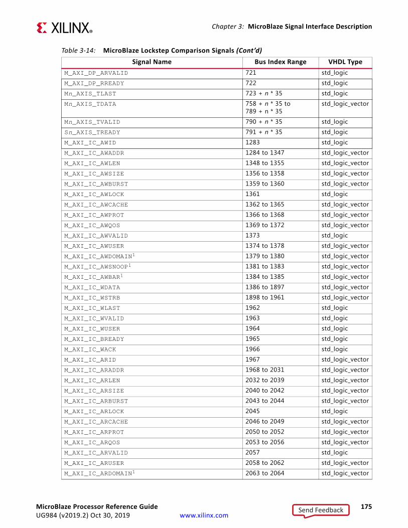
Chapter 3: MicroBlaze Signal Interface Description
M_AXI_DP_ARVALID 721 std_logic
M_AXI_DP_RREADY 722 std_logic
Mn_AXIS_TLAST 723 + n * 35 std_logic
Mn_AXIS_TDATA 758 + n * 35 to 789 + n * 35
std_logic_vector
Mn_AXIS_TVALID 790 + n * 35 std_logic
Sn_AXIS_TREADY 791 + n * 35 std_logic
M_AXI_IC_AWID 1283 std_logic
M_AXI_IC_AWADDR 1284 to 1347 std_logic_vector
M_AXI_IC_AWLEN 1348 to 1355 std_logic_vector
M_AXI_IC_AWSIZE 1356 to 1358 std_logic_vector
M_AXI_IC_AWBURST 1359 to 1360 std_logic_vector
M_AXI_IC_AWLOCK 1361 std_logic
M_AXI_IC_AWCACHE 1362 to 1365 std_logic_vector
M_AXI_IC_AWPROT 1366 to 1368 std_logic_vector
M_AXI_IC_AWQOS 1369 to 1372 std_logic_vector
M_AXI_IC_AWVALID 1373 std_logic
M_AXI_IC_AWUSER 1374 to 1378 std_logic_vector
M_AXI_IC_AWDOMAIN1 1379 to 1380 std_logic_vector
M_AXI_IC_AWSNOOP1 1381 to 1383 std_logic_vector
M_AXI_IC_AWBAR1 1384 to 1385 std_logic_vector
M_AXI_IC_WDATA 1386 to 1897 std_logic_vector
M_AXI_IC_WSTRB 1898 to 1961 std_logic_vector
M_AXI_IC_WLAST 1962 std_logic
M_AXI_IC_WVALID 1963 std_logic
M_AXI_IC_WUSER 1964 std_logic
M_AXI_IC_BREADY 1965 std_logic
M_AXI_IC_WACK 1966 std_logic
M_AXI_IC_ARID 1967 std_logic_vector
M_AXI_IC_ARADDR 1968 to 2031 std_logic_vector
M_AXI_IC_ARLEN 2032 to 2039 std_logic_vector
M_AXI_IC_ARSIZE 2040 to 2042 std_logic_vector
M_AXI_IC_ARBURST 2043 to 2044 std_logic_vector
M_AXI_IC_ARLOCK 2045 std_logic
M_AXI_IC_ARCACHE 2046 to 2049 std_logic_vector
M_AXI_IC_ARPROT 2050 to 2052 std_logic_vector
M_AXI_IC_ARQOS 2053 to 2056 std_logic_vector
M_AXI_IC_ARVALID 2057 std_logic
M_AXI_IC_ARUSER 2058 to 2062 std_logic_vector
M_AXI_IC_ARDOMAIN1 2063 to 2064 std_logic_vector
Table 3-14: MicroBlaze Lockstep Comparison Signals (Cont’d)Signal Name Bus Index Range VHDL Type
MicroBlaze Processor Reference Guide 175UG984 (v2019.2) Oct 30, 2019 www.xilinx.com
Send Feedback

Chapter 3: MicroBlaze Signal Interface Description
M_AXI_IC_ARSNOOP1 2065 to 2068 std_logic_vector
M_AXI_IC_ARBAR1 2069 to 2070 std_logic_vector
M_AXI_IC_RREADY 2071 std_logic
M_AXI_IC_RACK1 2072 std_logic
M_AXI_IC_ACREADY1 2073 std_logic
M_AXI_IC_CRVALID1 2074 std_logic
M_AXI_IC_CRRESP1 2075 to 2079 std_logic_vector
M_AXI_IC_CDVALID1 2080 std_logic
M_AXI_IC_CDLAST1 2081 std_logic
M_AXI_DC_AWID 2082 std_logic
M_AXI_DC_AWADDR 2083 to 2146 std_logic_vector
M_AXI_DC_AWLEN 2147 to 2154 std_logic_vector
M_AXI_DC_AWSIZE 2155 to 2157 std_logic_vector
M_AXI_DC_AWBURST 2158 to 2159 std_logic_vector
M_AXI_DC_AWLOCK 2160 std_logic
M_AXI_DC_AWCACHE 2161 to 2164 std_logic_vector
M_AXI_DC_AWPROT 2165 to 2167 std_logic_vector
M_AXI_DC_AWQOS 2168 to 2171 std_logic_vector
M_AXI_DC_AWVALID 2172 std_logic
M_AXI_DC_AWUSER 2172 to 2176 std_logic_vector
M_AXI_DC_AWDOMAIN1 2177 to 2178 std_logic_vector
M_AXI_DC_AWSNOOP1 2179 to 2182 std_logic_vector
M_AXI_DC_AWBAR1 2183 to 2184 std_logic_vector
M_AXI_DC_WDATA 2185 to 2696 std_logic_vector
M_AXI_DC_WSTRB 2697 to 2760 std_logic_vector
M_AXI_DC_WLAST 2761 std_logic
M_AXI_DC_WVALID 2762 std_logic
M_AXI_DC_WUSER 2863 std_logic
M_AXI_DC_BREADY 2764 std_logic
M_AXI_DC_WACK1 2765 std_logic
M_AXI_DC_ARID 2766 std_logic
M_AXI_DC_ARADDR 2767 to 2830 std_logic_vector
M_AXI_DC_ARLEN 2831 to 2838 std_logic_vector
M_AXI_DC_ARSIZE 2839 to 2841 std_logic_vector
M_AXI_DC_ARBURST 2842 to 2843 std_logic_vector
M_AXI_DC_ARLOCK 2844 std_logic
M_AXI_DC_ARCACHE 2845 to 2848 std_logic_vector
M_AXI_DC_ARPROT 2849 to 2851 std_logic_vector
M_AXI_DC_ARQOS 2852 to 2855 std_logic_vector
Table 3-14: MicroBlaze Lockstep Comparison Signals (Cont’d)Signal Name Bus Index Range VHDL Type
MicroBlaze Processor Reference Guide 176UG984 (v2019.2) Oct 30, 2019 www.xilinx.com
Send Feedback
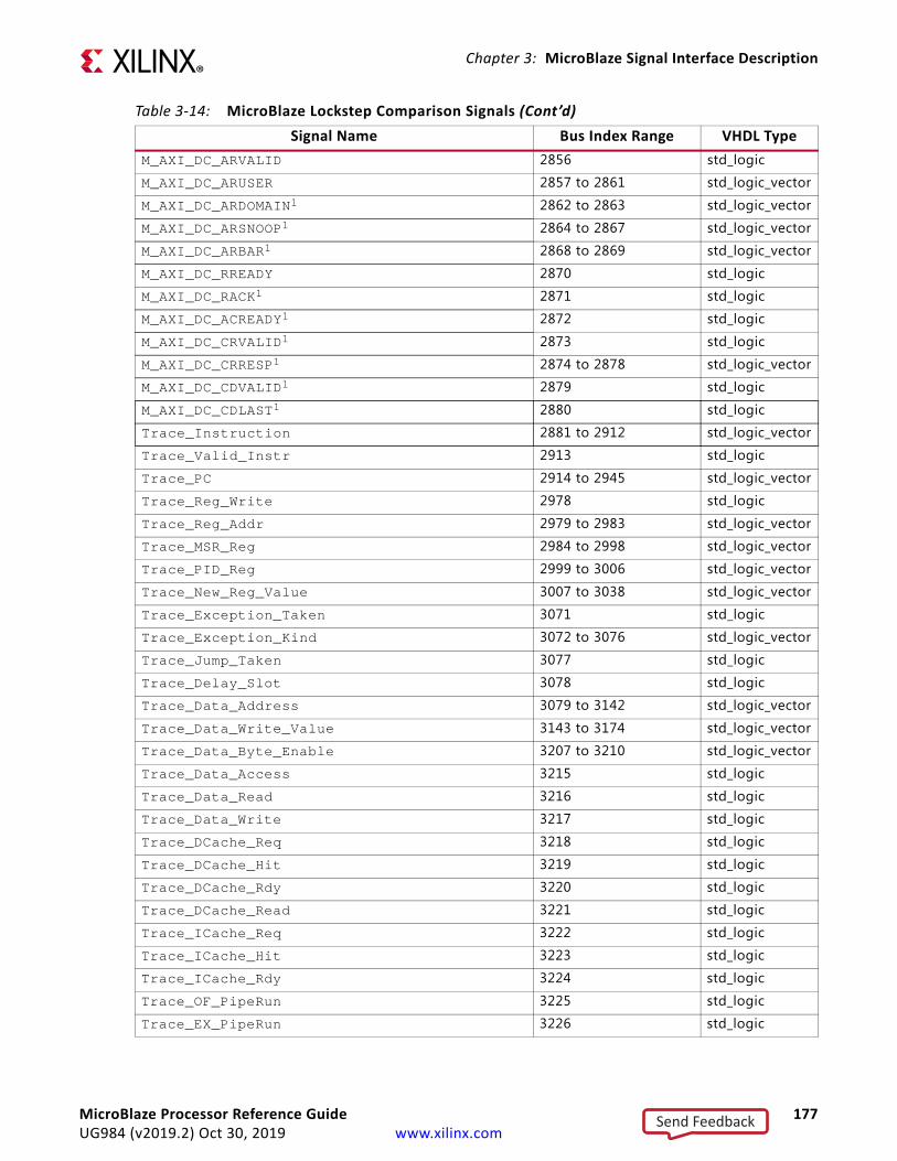
Chapter 3: MicroBlaze Signal Interface Description
M_AXI_DC_ARVALID 2856 std_logic
M_AXI_DC_ARUSER 2857 to 2861 std_logic_vector
M_AXI_DC_ARDOMAIN1 2862 to 2863 std_logic_vector
M_AXI_DC_ARSNOOP1 2864 to 2867 std_logic_vector
M_AXI_DC_ARBAR1 2868 to 2869 std_logic_vector
M_AXI_DC_RREADY 2870 std_logic
M_AXI_DC_RACK1 2871 std_logic
M_AXI_DC_ACREADY1 2872 std_logic
M_AXI_DC_CRVALID1 2873 std_logic
M_AXI_DC_CRRESP1 2874 to 2878 std_logic_vector
M_AXI_DC_CDVALID1 2879 std_logic
M_AXI_DC_CDLAST1 2880 std_logic
Trace_Instruction 2881 to 2912 std_logic_vector
Trace_Valid_Instr 2913 std_logic
Trace_PC 2914 to 2945 std_logic_vector
Trace_Reg_Write 2978 std_logic
Trace_Reg_Addr 2979 to 2983 std_logic_vector
Trace_MSR_Reg 2984 to 2998 std_logic_vector
Trace_PID_Reg 2999 to 3006 std_logic_vector
Trace_New_Reg_Value 3007 to 3038 std_logic_vector
Trace_Exception_Taken 3071 std_logic
Trace_Exception_Kind 3072 to 3076 std_logic_vector
Trace_Jump_Taken 3077 std_logic
Trace_Delay_Slot 3078 std_logic
Trace_Data_Address 3079 to 3142 std_logic_vector
Trace_Data_Write_Value 3143 to 3174 std_logic_vector
Trace_Data_Byte_Enable 3207 to 3210 std_logic_vector
Trace_Data_Access 3215 std_logic
Trace_Data_Read 3216 std_logic
Trace_Data_Write 3217 std_logic
Trace_DCache_Req 3218 std_logic
Trace_DCache_Hit 3219 std_logic
Trace_DCache_Rdy 3220 std_logic
Trace_DCache_Read 3221 std_logic
Trace_ICache_Req 3222 std_logic
Trace_ICache_Hit 3223 std_logic
Trace_ICache_Rdy 3224 std_logic
Trace_OF_PipeRun 3225 std_logic
Trace_EX_PipeRun 3226 std_logic
Table 3-14: MicroBlaze Lockstep Comparison Signals (Cont’d)Signal Name Bus Index Range VHDL Type
MicroBlaze Processor Reference Guide 177UG984 (v2019.2) Oct 30, 2019 www.xilinx.com
Send Feedback

Chapter 3: MicroBlaze Signal Interface Description
Debug Interface DescriptionThe debug interface on MicroBlaze is designed to work with the Xilinx Microprocessor Debug Module (MDM) IP core. The MDM is controlled by the Xilinx System Debugger (XSDB) through the JTAG port of the FPGA. The MDM can control multiple MicroBlaze processors at the same time. The debug signals are grouped in the DEBUG bus.
The debug interface can be grouped in the DEBUG bus, using either JTAG serial signals (by setting C_DEBUG_INTERFACE = 0) or the AXI4-Lite compatible parallel signals (by setting C_DEBUG_INTERFACE = 1). The MDM configuration must also be set accordingly.
It is also possible to use only AXI4-Lite parallel signals (C_DEBUG_INTERFACE = 2) grouped in an AXI4 bus, in case the MDM is not used. However, this configuration is not supported by the tools.
Table 3-15 lists the debug signals on MicroBlaze.
Trace_MEM_PipeRun 3227 std_logic
Trace_MB_Halted 3228 std_logic
Trace_Jump_Hit 3229 std_logic
Reserved 3230 to 40951. This signal is only used when C_INTERCONNECT = 3 (ACE).
Table 3-15: MicroBlaze Debug Signals Signal Name Description VHDL Type Kind
Dbg_Clk JTAG clock from MDM std_logic serial in
Dbg_TDI JTAG TDI from MDM std_logic serial in
Dbg_TDO JTAG TDO to MDM std_logic serial out
Dbg_Reg_En Debug register enable from MDM std_logic_vector serial in
Dbg_Shift1 JTAG BSCAN shift signal from MDM std_logic serial in
Dbg_Capture JTAG BSCAN capture signal from MDM std_logic serial in
Dbg_Update JTAG BSCAN update signal from MDM std_logic serial in
Debug_Rst1 Reset signal from MDM, active high. Should be held for at least 1 Clk clock cycle.
std_logic input
Dbg_Trig_In2 Cross trigger event input to MDM std_logic_vector output
Dbg_Trig_Ack_In2 Cross trigger event input acknowledge from MDM
std_logic_vector input
Dbg_Trig_Out2 Cross trigger action output from MDM std_logic_vector input
Dbg_Trig_Ack_Out2 Cross trigger action output acknowledge to MDM
std_logic_vector output
Table 3-14: MicroBlaze Lockstep Comparison Signals (Cont’d)Signal Name Bus Index Range VHDL Type
MicroBlaze Processor Reference Guide 178UG984 (v2019.2) Oct 30, 2019 www.xilinx.com
Send Feedback

Chapter 3: MicroBlaze Signal Interface Description
Dbg_Trace_Data3 External Program Trace data output to MDM std_logic_vector output
Dbg_Trace_Valid3 External Program Trace valid to MDM std_logic output
Dbg_Trace_Ready3 External Program Trace ready from MDM std_logic input
Dbg_Trace_Clk3 External Program Trace clock from MDM std_logic input
Dbg_ARADDR4 Read address from MDM std_logic_vector parallel in
Dbg_ARREADY4 Read address ready to MDM std_logic parallel out
Dbg_ARVALID4 Read address valid from MDM std_logic parallel in
Dbg_AWADDR4 Write address from MDM std_logic_vector parallel in
Dbg_AWREADY4 Write address ready to MDM std_logic parallel out
Dbg_AWVALID4 Write address valid from MDM std_logic parallel in
Dbg_BREADY4 Write response ready to MDM std_logic parallel out
Dbg_BRESP4 Write response to MDM std_logic_vector parallel out
Dbg_BVALID4 Write response valid from MDM std_logic parallel in
Dbg_RDATA4 Read data to MDM std_logic_vector parallel out
Dbg_RREADY4 Read data ready to MDM std_logic parallel out
Dbg_RRESP4 Read data response to MDM std_logic_vector parallel out
Dbg_RVALID4 Read data valid from MDM std_logic parallel in
Dbg_WDATA4 Write data from MDM std_logic_vector parallel in
Dbg_WREADY4 Write data ready to MDM std_logic parallel out
Dbg_WVALID4 Write data valid from MDM std_logic parallel in
DEBUG_ACLK4 Debug clock, must be same as Clk std_logic parallel in
DEBUG_ARESET4 Debug reset, must be same as Reset std_logic parallel in1. Updated for MicroBlaze v7.00: Dbg_Shift added and Debug_Rst included in DEBUG bus2. Updated for MicroBlaze v9.3: Dbg_Trig signals added to DEBUG bus3. Updated for MicroBlaze v9.4: External Program Trace signal added to DEBUG bus4. Updated for MicroBlaze v10.0: Parallel debug signals added to DEBUG bus
Table 3-15: MicroBlaze Debug Signals (Cont’d)Signal Name Description VHDL Type Kind
MicroBlaze Processor Reference Guide 179UG984 (v2019.2) Oct 30, 2019 www.xilinx.com
Send Feedback
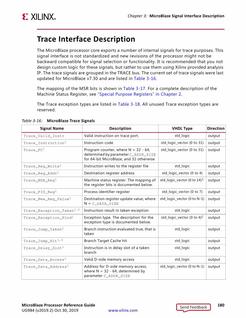
Chapter 3: MicroBlaze Signal Interface Description
Trace Interface DescriptionThe MicroBlaze processor core exports a number of internal signals for trace purposes. This signal interface is not standardized and new revisions of the processor might not be backward compatible for signal selection or functionality. It is recommended that you not design custom logic for these signals, but rather to use them using Xilinx provided analysis IP. The trace signals are grouped in the TRACE bus. The current set of trace signals were last updated for MicroBlaze v7.30 and are listed in Table 3-16.
The mapping of the MSR bits is shown in Table 3-17. For a complete description of the Machine Status Register, see “Special Purpose Registers” in Chapter 2.
The Trace exception types are listed in Table 3-18. All unused Trace exception types are reserved.
Table 3-16: MicroBlaze Trace Signals
Signal Name Description VHDL Type Direction
Trace_Valid_Instr Valid instruction on trace port. std_logic output
Trace_Instruction1 Instruction code std_logic_vector (0 to 31) output
Trace_PC1 Program counter, where N = 32 - 64, determined by parameter C_ADDR_SIZE for 64-bit MicroBlaze, and 32 otherwise
std_logic_vector (0 to 31) output
Trace_Reg_Write1 Instruction writes to the register file std_logic output
Trace_Reg_Addr1 Destination register address std_logic_vector (0 to 4) output
Trace_MSR_Reg1 Machine status register. The mapping of the register bits is documented below.
std_logic_vector (0 to 14)1 output
Trace_PID_Reg1 Process identifier register std_logic_vector (0 to 7) output
Trace_New_Reg_Value1 Destination register update value, where N = C_DATA_SIZE
std_logic_vector (0 to N-1) output
Trace_Exception_Taken1,2 Instruction result in taken exception std_logic output
Trace_Exception_Kind1 Exception type. The description for the exception type is documented below.
std_logic_vector (0 to 4)2 output
Trace_Jump_Taken1 Branch instruction evaluated true, that is taken
std_logic output
Trace_Jump_Hit1,3 Branch Target Cache hit std_logic output
Trace_Delay_Slot1 Instruction is in delay slot of a taken branch
std_logic output
Trace_Data_Access1 Valid D-side memory access std_logic output
Trace_Data_Address1 Address for D-side memory access, where N = 32 - 64, determined by parameter C_ADDR_SIZE
std_logic_vector (0 to N-1) output
MicroBlaze Processor Reference Guide 180UG984 (v2019.2) Oct 30, 2019 www.xilinx.com
Send Feedback

Chapter 3: MicroBlaze Signal Interface Description
Trace_Data_Write_Value1 Value for D-side memory write access, where N = C_DATA_SIZE
std_logic_vector (0 to N-1) output
Trace_Data_Byte_Enable1 Byte enables for D-side memory access,where N = C_DATA_SIZE / 8
std_logic_vector (0 to N-1) output
Trace_Data_Read1 D-side memory access is a read std_logic output
Trace_Data_Write1 D-side memory access is a write std_logic output
Trace_DCache_Req Data memory address is within D-Cache range. Set when a memory access instruction is executed.
std_logic output
Trace_DCache_Hit Data memory address is present in D-Cache. Set simultaneously with Trace_DCache_Req when a cache hit occurs.
std_logic output
Trace_DCache_Rdy Data memory address is within D-Cache range and the access is completed. Only set following a request with Trace_DCache_Req = 1 and Trace_DCache_Hit = 0.
std_logic output
Trace_DCache_Read The D-Cache request is a read. Valid only when Trace_DCache_Req = 1.
std_logic output
Trace_ICache_Req Instruction memory address is within I-Cache range, and the cache is enabled in the Machine Status Register. Set when an instruction is read into the instruction prefetch buffer.
std_logic output
Trace_ICache_Hit Instruction memory address is present in I-Cache. Set simultaneously with Trace_ICache_Req when a cache hit occurs.
std_logic output
Trace_ICache_Rdy • Instruction memory address is present in I-Cache. Set simultaneously with Trace_ICache_Req when a cache hit occurs in this case.
• Instruction memory address is within I-Cache range and the access is completed. Set following a request with Trace_ICache_Req = 1 and Trace_ICache_Hit = 0 in this case.
std_logic output
Trace_OF_PipeRun Pipeline advance for Decode stage std_logic output
Trace_EX_PipeRun3 Pipeline advance for Execution stage std_logic output
Trace_MEM_PipeRun3 Pipeline advance for Memory stage std_logic output
Trace_MB_Halted Pipeline is halted by debug std_logic output1. Valid only when Trace_Valid_Instr = 12. Valid only when Trace_Exception_Taken = 13. Not used with area optimization feature
Table 3-16: MicroBlaze Trace Signals (Cont’d)
Signal Name Description VHDL Type Direction
MicroBlaze Processor Reference Guide 181UG984 (v2019.2) Oct 30, 2019 www.xilinx.com
Send Feedback

Chapter 3: MicroBlaze Signal Interface Description
Table 3-17: Mapping of Trace MSR
Trace_MSR_Reg Machine Status Register
Bit Bit1
1. Bit numbers depend on if 64-bit MicroBlaze (C_DATA_SIZE = 64) is enabled or not.
Name Description
0 17 or 49 VMS Virtual Protected Mode Save
1 18 or 50 VM Virtual Protected Mode
2 19 or 51 UMS User Mode Save
3 20 or 52 UM User Mode
4 21 or 53 PVR Processor Version Register exists
5 22 or 54 EIP Exception In Progress
6 23 or 55 EE Exception Enable
7 24 or 56 DCE Data Cache Enable
8 25 or 57 DZO Division by Zero or Division Overflow
9 26 or 58 ICE Instruction Cache Enable
10 27 or 59 FSL AXI4-Stream Error
11 28 or 60 BIP Break in Progress
12 29 or 61 C Arithmetic Carry
13 30 or 62 IE Interrupt Enable
14 31 or 63 Reserved Reserved
Table 3-18: Type of Trace Exception
Trace_Exception_Kind [0:4] Description
00000 Stream exception
00001 Unaligned exception
00010 Illegal Opcode exception
00011 Instruction Bus exception
00100 Data Bus exception
00101 Divide exception
00110 FPU exception
00111 Privileged instruction exception
01010 Interrupt
01011 External non maskable break
01100 External maskable break
10000 Data storage exception
MicroBlaze Processor Reference Guide 182UG984 (v2019.2) Oct 30, 2019 www.xilinx.com
Send Feedback

Chapter 3: MicroBlaze Signal Interface Description
MicroBlaze Core ConfigurabilityThe MicroBlaze core has been developed to support a high degree of user configurability. This allows tailoring of the processor to meet specific cost/performance requirements.
Configuration is done using parameters that typically enable, size, or select certain processor features. For example, the instruction cache is enabled by setting the C_USE_ICACHE parameter. The size of the instruction cache, and the cacheable memory range, are all configurable using: C_CACHE_BYTE_SIZE, C_ICACHE_BASEADDR, and C_ICACHE_HIGHADDR respectively.
Parameters valid for the latest version of MicroBlaze are listed in Table 3-19. Not all of these are recognized by older versions of MicroBlaze; however, the configurability is fully backward compatible.
Note: Shaded rows indicate that the parameter has a fixed value and cannot be modified.
10001 Instruction storage exception
10010 Data TLB miss exception
10011 Instruction TLB miss exception
Table 3-18: Type of Trace Exception (Cont’d)
Trace_Exception_Kind [0:4] Description
Table 3-19: Configuration Parameters
Parameter Name Feature/Description Allowable Values
Default Value
Tool Assigned VHDL Type
C_FAMILY Target Family Listed in Table 3-20
virtex7 yes string
C_DATA_SIZE Data Size 32 = 32-bit MicroBlaze64 = 64-bit MicroBlaze
32, 64 32 integer
C_ADDR_SIZE Address Size 32-64 32 NA integer
C_DYNAMIC_BUS_SIZING Legacy 1 1 NA integer
C_SCO Xilinx internal 0 0 NA integer
C_AREA_OPTIMIZED Select implementation optimization:0 = Performance1 = Area2 = Frequency
0, 1, 2 0 integer
C_OPTIMIZATION Reserved for future use 0 0 NA integer
MicroBlaze Processor Reference Guide 183UG984 (v2019.2) Oct 30, 2019 www.xilinx.com
Send Feedback

Chapter 3: MicroBlaze Signal Interface Description
C_INTERCONNECT Select interconnect2 = AXI4 only3 = AXI4 and ACE
2, 3 2 integer
C_ENDIANNESS Select endianness1 = Little Endian
1 1 yes integer
C_BASE_VECTORS1 Configurable base vectors
0x0 - 0xFFFFFFFF FFFFFFFF
0x0 std_logic_vector
C_FAULT_TOLERANT Implement fault tolerance 0, 1 0 yes integer
C_ECC_USE_CE_EXCEPTION Generate exception for correctable ECC error 0,1 0 integer
C_LOCKSTEP_SLAVE Lockstep Slave 0, 1 0 integer
C_AVOID_PRIMITIVES Disallow FPGA primitives0 = None1 = SRL2 = LUTRAM3 = Both
0, 1, 2, 3 0
integer
C_ENABLE_DISCRETE_PORTS Show discrete ports 0, 1 0 integer
C_PVR Processor version register mode selection0 = None1 = Basic2 = Full
0, 1, 2 0
integer
C_PVR_USER1 Processor version register USER1 constant 0x00-0xff 0x00
std_logic_vector(0 to 7)
C_PVR_USER2 Processor version register USER2 constant 0x00000000
-0xffffffff0x00000000
std_logic_vector(0 to 31)
C_RESET_MSR_IE C_RESET_MSR_BIP
C_RESET_MSR_ICE
C_RESET_MSR_DCE
C_RESET_MSR_EE
C_RESET_MSR_EIP
Reset value for MSR register bits IE, BIP, ICE, DCE, EE, and EIP
Any combination
of the individual
bits
0x0000 std_logic
Table 3-19: Configuration Parameters (Cont’d)
Parameter Name Feature/Description Allowable Values
Default Value
Tool Assigned VHDL Type
MicroBlaze Processor Reference Guide 184UG984 (v2019.2) Oct 30, 2019 www.xilinx.com
Send Feedback
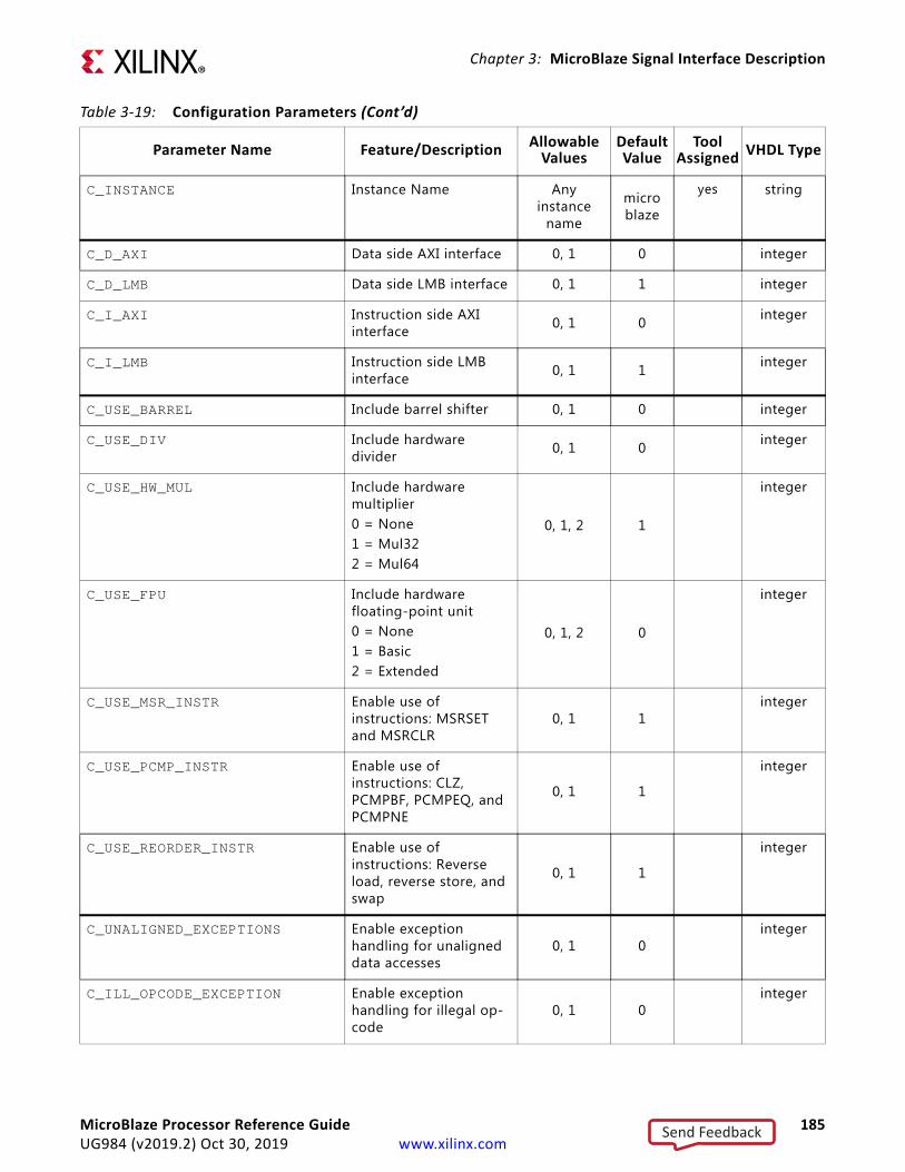
Chapter 3: MicroBlaze Signal Interface Description
C_INSTANCE Instance Name Any instance
name
microblaze
yes string
C_D_AXI Data side AXI interface 0, 1 0 integer
C_D_LMB Data side LMB interface 0, 1 1 integer
C_I_AXI Instruction side AXI interface 0, 1 0 integer
C_I_LMB Instruction side LMB interface 0, 1 1 integer
C_USE_BARREL Include barrel shifter 0, 1 0 integer
C_USE_DIV Include hardware divider 0, 1 0 integer
C_USE_HW_MUL Include hardware multiplier0 = None1 = Mul322 = Mul64
0, 1, 2 1
integer
C_USE_FPU Include hardware floating-point unit0 = None1 = Basic2 = Extended
0, 1, 2 0
integer
C_USE_MSR_INSTR Enable use of instructions: MSRSET and MSRCLR
0, 1 1integer
C_USE_PCMP_INSTR Enable use of instructions: CLZ, PCMPBF, PCMPEQ, and PCMPNE
0, 1 1
integer
C_USE_REORDER_INSTR Enable use of instructions: Reverse load, reverse store, and swap
0, 1 1
integer
C_UNALIGNED_EXCEPTIONS Enable exception handling for unaligned data accesses
0, 1 0integer
C_ILL_OPCODE_EXCEPTION Enable exception handling for illegal op-code
0, 1 0integer
Table 3-19: Configuration Parameters (Cont’d)
Parameter Name Feature/Description Allowable Values
Default Value
Tool Assigned VHDL Type
MicroBlaze Processor Reference Guide 185UG984 (v2019.2) Oct 30, 2019 www.xilinx.com
Send Feedback

Chapter 3: MicroBlaze Signal Interface Description
C_M_AXI_I_BUS_EXCEPTION Enable exception handling for M_AXI_I bus error
0, 1 0integer
C_M_AXI_D_BUS_EXCEPTION Enable exception handling for M_AXI_D bus error
0, 1 0integer
C_DIV_ZERO_EXCEPTION Enable exception handling for division by zero or division overflow
0, 1 0
integer
C_FPU_EXCEPTION Enable exception handling for hardware floating-point unit exceptions
0, 1 0
integer
C_OPCODE_0x0_ILLEGAL Detect opcode 0x0 as an illegal instruction 0,1 0 integer
C_FSL_EXCEPTION Enable exception handling for Stream Links
0,1 0integer
C_ECC_USE_CE_EXCEPTION Generate Bus Error Exceptions for correctable errors
0,1 0integer
C_USE_STACK_PROTECTION Generate exception for stack overflow or stack underflow
0,1 0integer
C_IMPRECISE_EXCEPTIONS Allow imprecise exceptions for ECC errors in LMB memory
0,1 0integer
C_DEBUG_ENABLED MDM Debug interface0 = None1 = Basic2 = Extended
0,1,2 1
integer
C_NUMBER_OF_PC_BRK Number of hardware breakpoints 0-8 1 integer
C_NUMBER_OF_RD_ADDR_BRK Number of read address watchpoints 0-4 0 integer
C_NUMBER_OF_WR_ADDR_BRK Number of write address watchpoints 0-4 0 integer
C_DEBUG_EVENT_COUNTERS Number of Performance Monitor event counters 0-48 5 integer
Table 3-19: Configuration Parameters (Cont’d)
Parameter Name Feature/Description Allowable Values
Default Value
Tool Assigned VHDL Type
MicroBlaze Processor Reference Guide 186UG984 (v2019.2) Oct 30, 2019 www.xilinx.com
Send Feedback

Chapter 3: MicroBlaze Signal Interface Description
C_DEBUG_LATENCY_COUNTERS Number of Performance Monitor latency counters
0-7 1 integer
C_DEBUG_COUNTER_WIDTH Performance Monitor counter width 32,48,64 32 integer
C_DEBUG_TRACE_SIZE Trace Buffer sizeEmbedded: 0, ≥ 8192External: 0, 32 - 8192
0, 32, 64, 128, 256,
8192, 16384, 32768, 65536, 131072
8192 integer
C_DEBUG_PROFILE_SIZE Profile Buffer size 0, 4096, 8192,
16384, 32768, 65536, 131072
0 integer
C_DEBUG_EXTERNAL_TRACE External Program Trace 0,1 0 yes integer
C_DEBUG_INTERFACE Debug Interface:0 = Debug Serial1 = Debug Parallel2 = AXI4-Lite
0,1,2 0 integer
C_ASYNC_INTERRUPT Asynchronous Interrupt 0,1 0 yes integer
C_ASYNC_WAKEUP Asynchronous Wakeup 00,01,10,11 00 yes integer
C_INTERRUPT_IS_EDGE Level/Edge Interrupt 0, 1 0 yes integer
C_EDGE_IS_POSITIVE Negative/Positive Edge Interrupt 0, 1 1 yes integer
C_FSL_LINKS Number of AXI-Stream interfaces 0-16 0 integer
C_USE_EXTENDED_FSL_INSTR Enable use of extended stream instructions 0, 1 0 integer
C_ICACHE_BASEADDR Instruction cache base address
0x0 - 0xFFFFFFFF FFFFFFFF
0x0 std_logic_vector
C_ICACHE_HIGHADDR Instruction cache high address
0x0 - 0xFFFFFFFF FFFFFFFF
0x3FFFFFFF
std_logic_vector
C_USE_ICACHE Instruction cache 0, 1 0 integer
Table 3-19: Configuration Parameters (Cont’d)
Parameter Name Feature/Description Allowable Values
Default Value
Tool Assigned VHDL Type
MicroBlaze Processor Reference Guide 187UG984 (v2019.2) Oct 30, 2019 www.xilinx.com
Send Feedback
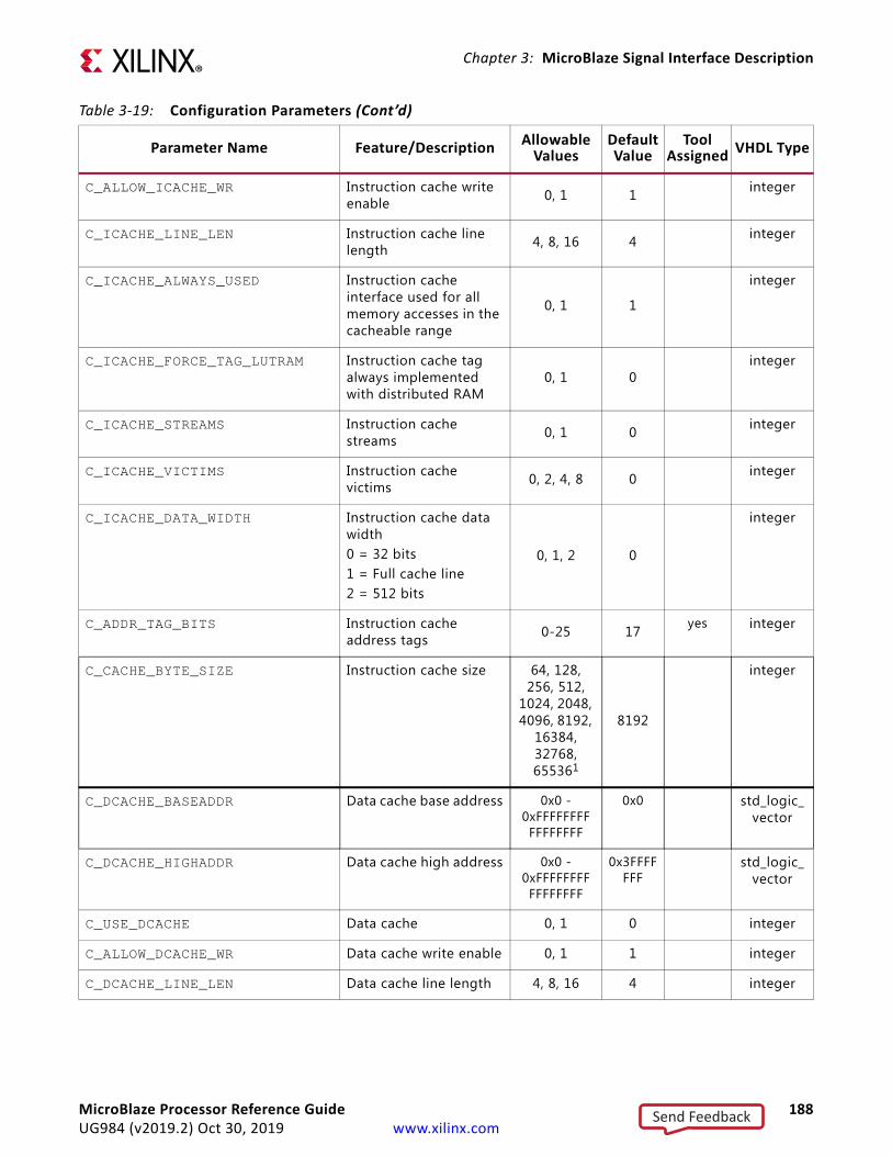
Chapter 3: MicroBlaze Signal Interface Description
C_ALLOW_ICACHE_WR Instruction cache write enable 0, 1 1 integer
C_ICACHE_LINE_LEN Instruction cache line length 4, 8, 16 4 integer
C_ICACHE_ALWAYS_USED Instruction cache interface used for all memory accesses in the cacheable range
0, 1 1
integer
C_ICACHE_FORCE_TAG_LUTRAM Instruction cache tag always implemented with distributed RAM
0, 1 0integer
C_ICACHE_STREAMS Instruction cache streams 0, 1 0 integer
C_ICACHE_VICTIMS Instruction cache victims 0, 2, 4, 8 0 integer
C_ICACHE_DATA_WIDTH Instruction cache data width0 = 32 bits1 = Full cache line2 = 512 bits
0, 1, 2 0
integer
C_ADDR_TAG_BITS Instruction cache address tags 0-25 17 yes integer
C_CACHE_BYTE_SIZE Instruction cache size 64, 128, 256, 512,
1024, 2048, 4096, 8192,
16384, 32768, 655361
8192
integer
C_DCACHE_BASEADDR Data cache base address 0x0 - 0xFFFFFFFF FFFFFFFF
0x0 std_logic_vector
C_DCACHE_HIGHADDR Data cache high address 0x0 - 0xFFFFFFFF FFFFFFFF
0x3FFFFFFF
std_logic_vector
C_USE_DCACHE Data cache 0, 1 0 integer
C_ALLOW_DCACHE_WR Data cache write enable 0, 1 1 integer
C_DCACHE_LINE_LEN Data cache line length 4, 8, 16 4 integer
Table 3-19: Configuration Parameters (Cont’d)
Parameter Name Feature/Description Allowable Values
Default Value
Tool Assigned VHDL Type
MicroBlaze Processor Reference Guide 188UG984 (v2019.2) Oct 30, 2019 www.xilinx.com
Send Feedback
Chapter 3: MicroBlaze Signal Interface Description
C_DCACHE_ALWAYS_USED Data cache interface used for all accesses in the cacheable range
0, 1 1integer
C_DCACHE_FORCE_TAG_LUTRAM Data cache tag always implemented with distributed RAM
0, 1 0integer
C_DCACHE_USE_WRITEBACK Data cache write-back storage policy used 0, 1 0 integer
C_DCACHE_VICTIMS Data cache victims 0, 2, 4, 8 0 integer
C_DCACHE_DATA_WIDTH Data cache data width0 = 32 bits 1 = Full cache line 2 = 512 bits
0, 1, 2 0
integer
C_DCACHE_ADDR_TAG Data cache address tags 0-25 17 yes integer
C_DCACHE_BYTE_SIZE Data cache size 64, 128, 256, 512,
1024, 2048, 4096, 8192,
16384, 32768, 655362
8192
integer
C_USE_MMU3 Memory Management:0 = None1 = User Mode2 = Protection3 = Virtual
0, 1, 2, 3 0 integer
C_MMU_DTLB_SIZE3 Data shadow Translation Look-Aside Buffer size 1, 2, 4, 8 4 integer
C_MMU_ITLB_SIZE3 Instruction shadow Translation Look-Aside Buffer size
1, 2, 4, 8 2 integer
C_MMU_TLB_ACCESS3 Access to memory management special registers:0 = Minimal1 = Read2 = Write3 = Full
0, 1, 2, 3 3 integer
C_MMU_ZONES3 Number of memory protection zones 0-16 16 integer
Table 3-19: Configuration Parameters (Cont’d)
Parameter Name Feature/Description Allowable Values
Default Value
Tool Assigned VHDL Type
MicroBlaze Processor Reference Guide 189UG984 (v2019.2) Oct 30, 2019 www.xilinx.com
Send Feedback
Chapter 3: MicroBlaze Signal Interface Description
C_MMU_PRIVILEGED_INSTR3 Privileged instructions0 = Full protection1 = Allow stream instrs2 = Allow extended addr3 = Allow both
0,1,2,3 0 integer
C_USE_INTERRUPT Enable interrupt handling0 = No interrupt1 = Standard interrupt2 = Low-latency interrupt
0, 1, 2 1 yes integer
C_USE_EXT_BRK Enable external break handling 0,1 0 yes integer
C_USE_EXT_NM_BRK Enable external non-maskable break handling
0,1 0 yes integer
C_USE_NON_SECURE Use corresponding non-secure input 0-15 0 yes integer
C_USE_BRANCH_TARGET_CACHE3 Enable Branch Target Cache 0,1 0 integer
C_BRANCH_TARGET_CACHE_SIZE3 Branch Target Cache size:0 = Default1 = 8 entries2 = 16 entries3 = 32 entries4 = 64 entries5 = 512 entries6 = 1024 entries7 = 2048 entries
0-7 0 integer
C_M_AXI_DP_ THREAD_ID_WIDTH
Data side AXI thread ID width 1 1 integer
C_M_AXI_DP_DATA_WIDTH Data side AXI data width 32 32 integer
C_M_AXI_DP_ADDR_WIDTH Data side AXI address width 32-64 32 yes integer
C_M_AXI_DP_ SUPPORTS_THREADS
Data side AXI uses threads 0 0 integer
C_M_AXI_DP_SUPPORTS_READ Data side AXI support for read accesses 1 1 integer
Table 3-19: Configuration Parameters (Cont’d)
Parameter Name Feature/Description Allowable Values
Default Value
Tool Assigned VHDL Type
MicroBlaze Processor Reference Guide 190UG984 (v2019.2) Oct 30, 2019 www.xilinx.com
Send Feedback

Chapter 3: MicroBlaze Signal Interface Description
C_M_AXI_DP_SUPPORTS_WRITE Data side AXI support for write accesses 1 1 integer
C_M_AXI_DP_SUPPORTS_ NARROW_BURST
Data side AXI narrow burst support 0 0 integer
C_M_AXI_DP_PROTOCOL Data side AXI protocol AXI4, AXI4LITE
AXI4LITE
yes string
C_M_AXI_DP_ EXCLUSIVE_ACCESS
Data side AXI exclusive access support 0,1 0 integer
C_M_AXI_IP_ THREAD_ID_WIDTH
Instruction side AXI thread ID width 1 1 integer
C_M_AXI_IP_DATA_WIDTH Instruction side AXI data width 32 32 integer
C_M_AXI_IP_ADDR_WIDTH Instruction side AXI address width 32-64 32 yes integer
C_M_AXI_IP_ SUPPORTS_THREADS
Instruction side AXI uses threads 0 0 integer
C_M_AXI_IP_SUPPORTS_READ Instruction side AXI support for read accesses
1 1integer
C_M_AXI_IP_SUPPORTS_WRITE Instruction side AXI support for write accesses
0 0integer
C_M_AXI_IP_SUPPORTS_ NARROW_BURST
Instruction side AXI narrow burst support 0 0 integer
C_M_AXI_IP_PROTOCOL Instruction side AXI protocol AXI4LITE AXI4
LITEstring
C_M_AXI_DC_ THREAD_ID_WIDTH
Data cache AXI ID width 1 1 integer
C_M_AXI_DC_DATA_WIDTH Data cache AXI data width
32, 64, 128, 256, 512 32 integer
C_M_AXI_DC_ADDR_WIDTH Data cache AXI address width 32-64 32 yes integer
C_M_AXI_DC_ SUPPORTS_THREADS
Data cache AXI uses threads 0 0 integer
C_M_AXI_DC_SUPPORTS_READ Data cache AXI support for read accesses 1 1 integer
C_M_AXI_DC_SUPPORTS_WRITE Data cache AXI support for write accesses 1 1 integer
Table 3-19: Configuration Parameters (Cont’d)
Parameter Name Feature/Description Allowable Values
Default Value
Tool Assigned VHDL Type
MicroBlaze Processor Reference Guide 191UG984 (v2019.2) Oct 30, 2019 www.xilinx.com
Send Feedback

Chapter 3: MicroBlaze Signal Interface Description
C_M_AXI_DC_SUPPORTS_ NARROW_BURST
Data cache AXI narrow burst support 0 0 integer
C_M_AXI_DC_SUPPORTS_ USER_SIGNALS
Data cache AXI user signal support 1 1 integer
C_M_AXI_DC_PROTOCOL Data cache AXI protocol AXI4 AXI4 string
C_M_AXI_DC_AWUSER_WIDTH Data cache AXI user width 5 5 integer
C_M_AXI_DC_ARUSER_WIDTH Data cache AXI user width 5 5 integer
C_M_AXI_DC_WUSER_WIDTH Data cache AXI user width 1 1 integer
C_M_AXI_DC_RUSER_WIDTH Data cache AXI user width 1 1 integer
C_M_AXI_DC_BUSER_WIDTH Data cache AXI user width 1 1 integer
C_M_AXI_DC_ EXCLUSIVE_ACCESS
Data cache AXI exclusive access support 0,1 0 integer
C_M_AXI_DC_USER_VALUE Data cache AXI user value 0-31 31 integer
C_M_AXI_IC_ THREAD_ID_WIDTH
Instruction cache AXI ID width 1 1 integer
C_M_AXI_IC_DATA_WIDTH Instruction cache AXI data width
32, 64, 128, 256, 512 32 integer
C_M_AXI_IC_ADDR_WIDTH Instruction cache AXI address width 32-64 32 yes integer
C_M_AXI_IC_ SUPPORTS_THREADS
Instruction cache AXI uses threads 0 0 integer
C_M_AXI_IC_SUPPORTS_READ Instruction cache AXI support for read accesses
1 1integer
C_M_AXI_IC_SUPPORTS_WRITE Instruction cache AXI support for write accesses
0 0integer
C_M_AXI_IC_SUPPORTS_ NARROW_BURST
Instruction cache AXI narrow burst support 0 0 integer
C_M_AXI_IC_SUPPORTS_ USER_SIGNALS
Instruction cache AXI user signal support 1 1 integer
Table 3-19: Configuration Parameters (Cont’d)
Parameter Name Feature/Description Allowable Values
Default Value
Tool Assigned VHDL Type
MicroBlaze Processor Reference Guide 192UG984 (v2019.2) Oct 30, 2019 www.xilinx.com
Send Feedback
Chapter 3: MicroBlaze Signal Interface Description
C_M_AXI_IC_PROTOCOL Instruction cache AXI protocol AXI4 AXI4 string
C_M_AXI_IC_AWUSER_WIDTH Instruction cache AXI user width 5 5 integer
C_M_AXI_IC_ARUSER_WIDTH Instruction cache AXI user width 5 5 integer
C_M_AXI_IC_WUSER_WIDTH Instruction cache AXI user width 1 1 integer
C_M_AXI_IC_RUSER_WIDTH Instruction cache AXI user width 1 1 integer
C_M_AXI_IC_BUSER_WIDTH Instruction cache AXI user width 1 1 integer
C_M_AXI_IC_USER_VALUE Instruction cache AXI user value 0-31 31 integer
C_STREAM_INTERCONNECT Select AXI4-Stream interconnect 0,1 0 integer
C_Mn_AXIS_PROTOCOL AXI4-Stream protocol GENERIC GENERIC string
C_Sn_AXIS_PROTOCOL AXI4-Stream protocol GENERIC GENERIC string
C_Mn_AXIS_DATA_WIDTH AXI4-Stream master data width 32 32 NA integer
C_Sn_AXIS_DATA_WIDTH AXI4-Stream slave data width 32 32 NA integer
C_NUM_SYNC_FF_CLK Reset and Wakeup[0:1] synchronization stages ≥0 2 integer
C_NUM_SYNC_FF_CLK_IRQ Interrupt input signal synchronization stages ≥0 1 integer
C_NUM_SYNC_FF_CLK_DEBUG Dbg_ serial signal synchronization stages ≥0 2 integer
C_NUM_SYNC_FF_DBG_CLK Internal synchronization stages to Dbg_Clk ≥0 1 integer
C_NUM_SYNC_FF_DBG_TRACE_CLK Internal synchronization stages to Dbg_Trace_Clk ≥0 1 integer
1. The 7 least significant bits must all be 0.2. Not all sizes are permitted in all architectures. The cache uses 0 - 32 RAMB primitives (0 if cache size is less than 2048).3. Not available when C_AREA_OPTIMIZED is set to 1 (Area).
1.
Table 3-19: Configuration Parameters (Cont’d)
Parameter Name Feature/Description Allowable Values
Default Value
Tool Assigned VHDL Type
MicroBlaze Processor Reference Guide 193UG984 (v2019.2) Oct 30, 2019 www.xilinx.com
Send Feedback

Chapter 3: MicroBlaze Signal Interface Description
Table 3-20: Parameter C_FAMILY Allowable Values
Allowable Values
Artix® aartix7 artix7 artix7l qartix7 qartix7l
Kintex® kintex7 kintex7l qkintex7 qkintex7l kintexu kintexuplus
Spartan® spartan7
Virtex® qvirtex7 virtex7 virtexu virtexuplus virtexuplusHBM
Zynq® azynq zynq qzynq zynquplus zynquplusRFSOC
MicroBlaze Processor Reference Guide 194UG984 (v2019.2) Oct 30, 2019 www.xilinx.com
Send Feedback

Chapter 4
MicroBlaze Application Binary Interface
IntroductionThis chapter describes MicroBlaze™ Application Binary Interface (ABI), which is important for developing software in assembly language for the soft processor. The MicroBlaze GNU compiler follows the conventions described in this document. Any code written by assembly programmers should also follow the same conventions to be compatible with the compiler generated code. Interrupt and Exception handling is also explained briefly.
Data TypesThe data types used by MicroBlaze assembly programs are shown in the following table. Data types such as data8, data16, data32, and data64 are used in place of the usual byte, half-word, and word.register.
Table 4-1: Data Types in MicroBlaze Assembly Programs
MicroBlaze data types (for assembly programs)
Corresponding ANSI C data types32-bit MicroBlaze
Corresponding ANSI C data types64-bit MicroBlaze
Size (bytes)
data8 char char 1
data16 short short 2
data32 int int 4
long int - 4
float float 4
enum enum 4
data16/data32 pointer1
1. Pointers to small data areas, which can be accessed by global pointers are data16.
- 2/4
data64 - long int 8
long long int long long int 8
- double 8
- pointer 8
MicroBlaze Processor Reference Guide 195UG984 (v2019.2) Oct 30, 2019 www.xilinx.com
Send Feedback

Chapter 4: MicroBlaze Application Binary Interface
Register Usage ConventionsThe register usage convention for MicroBlaze is given in the following table.
Table 4-2: Register Usage Conventions
Register Type Enforcement PurposeR0 Dedicated HW Value 0
R1 Dedicated SW Stack Pointer
R2 Dedicated SW Read-only small data area anchor
R3-R4 Volatile SW Return Values/Temporaries
R5-R10 Volatile SW Passing parameters/Temporaries
R11-R12 Volatile SW Temporaries
R13 Dedicated SW Read-write small data area anchor
R14 Dedicated HW Return address for Interrupt
R15 Dedicated SW Return address for Sub-routine
R16 Dedicated HW Return address for Trap (Debugger)
R17 Dedicated HW/SW Return address for Exceptions HW, if configured to support hardware exceptions, else SW
R18 Dedicated SW Reserved for Assembler/Compiler Temporaries
R19 Non-volatile SW Must be saved across function calls. Callee-save
R20 Dedicatedor
Non-volatile
SW Reserved for storing a pointer to the global offset table (GOT) in position independent code (PIC). Non-volatile in non-PIC code. Must be saved across function calls. Callee-save.
R21-R31 Non-volatile SW Must be saved across function calls. Callee-save.
RPC Special HW Program counter
RMSR Special HW Machine Status Register
REAR Special HW Exception Address Register
RESR Special HW Exception Status Register
RFSR Special HW Floating-Point Status Register
RBTR Special HW Branch Target Register
REDR Special HW Exception Data Register
RPID Special HW Process Identifier Register
RZPR Special HW Zone Protection Register
RTLBLO Special HW Translation Look-Aside Buffer Low Register
RTLBHI Special HW Translation Look-Aside Buffer High Register
RTLBX Special HW Translation Look-Aside Buffer Index Register
RTLBSX Special HW Translation Look-Aside Buffer Search Index
RPVR0-12 Special HW Processor Version Register 0 through 12
MicroBlaze Processor Reference Guide 196UG984 (v2019.2) Oct 30, 2019 www.xilinx.com
Send Feedback
Chapter 4: MicroBlaze Application Binary Interface
The architecture for MicroBlaze defines 32 general purpose registers (GPRs). These registers are classified as volatile, non-volatile, and dedicated.
• The volatile registers (also known as caller-save) are used as temporaries and do not retain values across the function calls. Registers R3 through R12 are volatile, of which R3 and R4 are used for returning values to the caller function, if any. Registers R5 through R10 are used for passing parameters between subroutines.
• Registers R19 through R31 retain their contents across function calls and are hence termed as non-volatile registers (a.k.a callee-save). The callee function is expected to save those non-volatile registers, which are being used. These are typically saved to the stack during the prologue and then reloaded during the epilogue.
• Certain registers are used as dedicated registers and programmers are not expected to use them for any other purpose.
- Registers R14 through R17 are used for storing the return address from interrupts, sub-routines, traps, and exceptions in that order. Subroutines are called using the branch and link instruction, which saves the current Program Counter (PC) onto register R15.
- Small data area pointers are used for accessing certain memory locations with 16- bit immediate value. These areas are discussed in the memory model section of this document. The read only small data area (SDA) anchor R2 (Read-Only) is used to access the constants such as literals. The other SDA anchor R13 (Read-Write) is used for accessing the values in the small data read-write section.
- Register R1 stores the value of the stack pointer and is updated on entry and exit from functions.
- Register R18 is used as a temporary register for assembler operations.
• MicroBlaze includes special purpose registers such as:
- program counter (rpc)
- machine status register (rmsr)
- exception status register (resr)
- exception address register (rear)
- floating-point status register (rfsr), branch target register (rbtr)
- exception data register (redr)
- memory management registers (rpid, rzpr, rtlblo, rtlbhi, rtlbx, rtlbsx)
- processor version registers (0-12)
These registers are not mapped directly to the register file; and hence, the usage of these registers is different from the general purpose registers. The value of a special purpose registers can be transferred to or from a general purpose register by using mts and mfs instructions respectively.
MicroBlaze Processor Reference Guide 197UG984 (v2019.2) Oct 30, 2019 www.xilinx.com
Send Feedback
Chapter 4: MicroBlaze Application Binary Interface
Stack ConventionThe stack conventions used by MicroBlaze are detailed in Table 4-3.
The shaded area in Table 4-3 denotes a part of the stack frame for a caller function, while the unshaded area indicates the callee frame function. The ABI conventions of the stack frame define the protocol for passing parameters, preserving non-volatile register values, and allocating space for the local variables in a function.
Functions that contain calls to other subroutines are called as non-leaf functions. These non-leaf functions have to create a new stack frame area for its own use. When the program starts executing, the stack pointer has the maximum value. As functions are called, the stack pointer is decremented by the number of words required by every function for its stack frame. The stack pointer of a caller function always has a higher value as compared to the callee function.
Table 4-3: Stack Convention
Consider an example where Func1 calls Func2, which in turn calls Func3. The stack representation at different instances is depicted in Figure 4-1. After the call from Func 1 to Func 2, the value of the stack pointer (SP) is decremented. This value of SP is again decremented to accommodate the stack frame for Func3. On return from Func 3 the value of the stack pointer is increased to its original value in the function, Func 2.
High Address
Function Parameters for called sub-routine (Arg n .. Arg1)(Optional: Maximum number of arguments required for any called procedure from the current procedure).
Old Stack Pointer
Link Register (R15)
Callee Saved Register (R31....R19)(Optional: Only those registers which are used by the current procedure are saved)
Local Variables for Current Procedure(Optional: Present only if Locals defined in the procedure)
Functional Parameters (Arg n .. Arg 1)(Optional: Maximum number of arguments required for any called procedure from the current procedure)
New Stack Pointer
Link Register
Low Address
MicroBlaze Processor Reference Guide 198UG984 (v2019.2) Oct 30, 2019 www.xilinx.com
Send Feedback
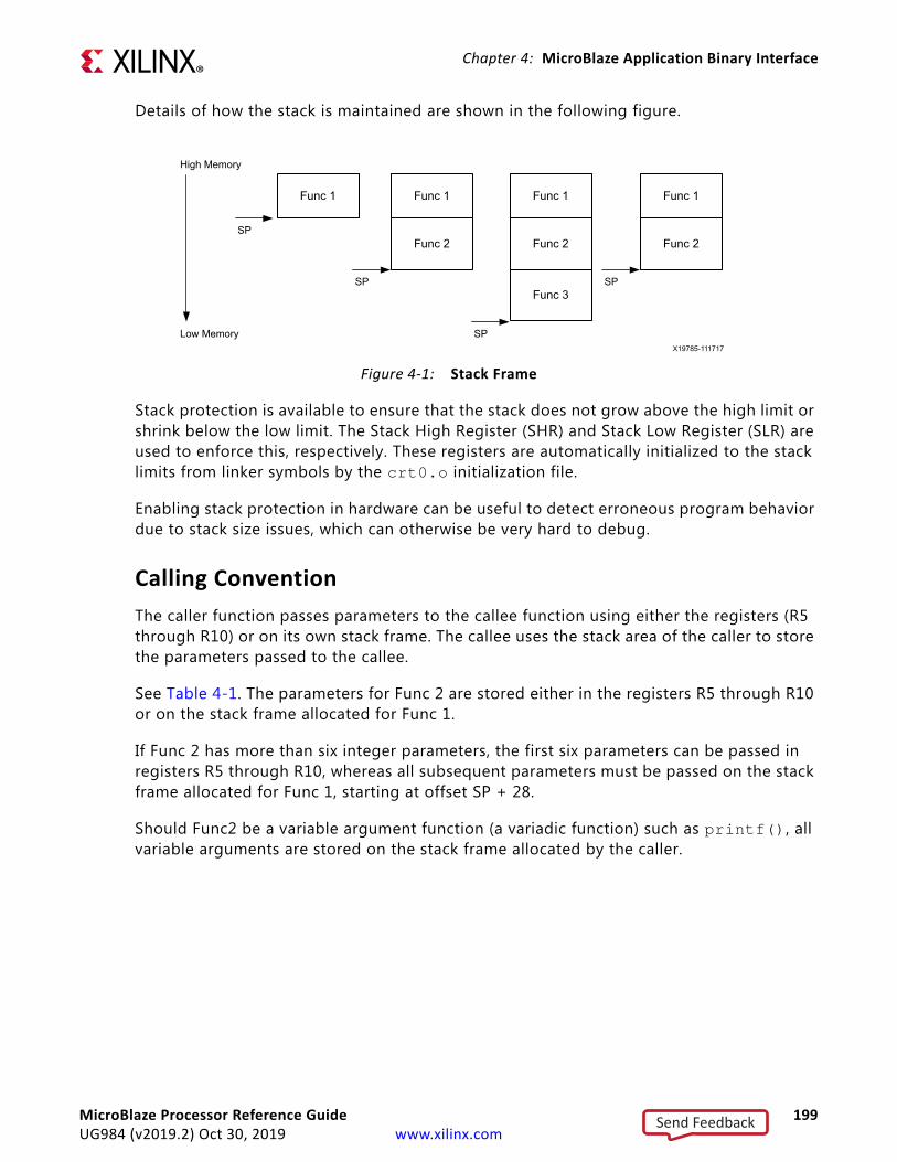
Chapter 4: MicroBlaze Application Binary Interface
Details of how the stack is maintained are shown in the following figure.
Stack protection is available to ensure that the stack does not grow above the high limit or shrink below the low limit. The Stack High Register (SHR) and Stack Low Register (SLR) are used to enforce this, respectively. These registers are automatically initialized to the stack limits from linker symbols by the crt0.o initialization file.
Enabling stack protection in hardware can be useful to detect erroneous program behavior due to stack size issues, which can otherwise be very hard to debug.
Calling ConventionThe caller function passes parameters to the callee function using either the registers (R5 through R10) or on its own stack frame. The callee uses the stack area of the caller to store the parameters passed to the callee.
See Table 4-1. The parameters for Func 2 are stored either in the registers R5 through R10 or on the stack frame allocated for Func 1.
If Func 2 has more than six integer parameters, the first six parameters can be passed in registers R5 through R10, whereas all subsequent parameters must be passed on the stack frame allocated for Func 1, starting at offset SP + 28.
Should Func2 be a variable argument function (a variadic function) such as printf(), all variable arguments are stored on the stack frame allocated by the caller.
X-Ref Target - Figure 4-1
Figure 4-1: Stack Frame
Func 1
High Memory
SP
Func 1
SP
Func 2
Func 1
SP
Func 2
Func 3
Func 1
SP
Func 2
Low MemoryX19785-111717
MicroBlaze Processor Reference Guide 199UG984 (v2019.2) Oct 30, 2019 www.xilinx.com
Send Feedback
Chapter 4: MicroBlaze Application Binary Interface
Memory ModelThe memory model for MicroBlaze classifies the data into four different parts: Small Data Area, Data Area, Common Un-Initialized Area, and Literals or Constants.
Small Data AreaGlobal initialized variables which are small in size are stored in this area. The threshold for deciding the size of the variable to be stored in the small data area is set to 8 bytes in the MicroBlaze C compiler (mb-gcc), but this can be changed by giving a command line option to the compiler. Details about this option are discussed in the “GNU Compiler Tools” chapter of the Embedded System Tools Reference Manual (UG1043) [Ref 13]. 64 kilobytes of memory is allocated for the small data areas. The small data area is accessed using the read-write small data area anchor (R13) and a 16-bit offset. Allocating small variables to this area reduces the requirement of adding IMM instructions to the code for accessing global variables. Any variable in the small data area can also be accessed using an absolute address.
Data AreaComparatively large initialized variables are allocated to the data area, which can either be accessed using the read-write SDA anchor R13 or using the absolute address, depending on the command line option given to the compiler.
Common Un-Initialized AreaUn-initialized global variables are allocated in the common area and can be accessed either using the absolute address or using the read-write small data area anchor R13.
Literals or ConstantsConstants are placed into the read-only small data area and are accessed using the read-only small data area anchor R2.
The compiler generates appropriate global pointers to act as base pointers. The actual values of the SDA anchors are decided by the linker, in the final linking stages. For more information on the various sections of the memory see the “MicroBlaze Linker Scripts” section and Appendix B of the Embedded System Tools Reference Manual (UG1043) [Ref 13].
The compiler generates appropriate sections, depending on the command line options. See the “GNU Compiler Tools” chapter in the Embedded System Tools Reference Manual (UG1043) [Ref 13] for more information about these options.
MicroBlaze Processor Reference Guide 200UG984 (v2019.2) Oct 30, 2019 www.xilinx.com
Send Feedback
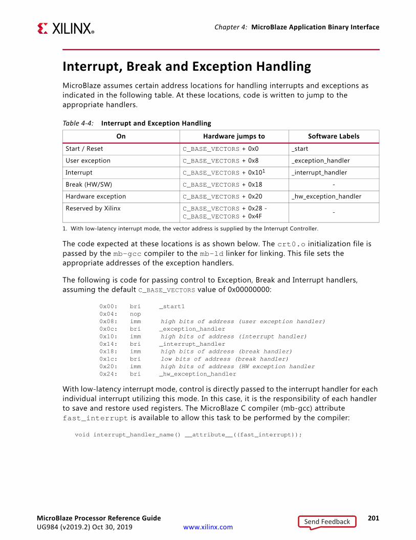
Chapter 4: MicroBlaze Application Binary Interface
Interrupt, Break and Exception HandlingMicroBlaze assumes certain address locations for handling interrupts and exceptions as indicated in the following table. At these locations, code is written to jump to the appropriate handlers.
The code expected at these locations is as shown below. The crt0.o initialization file is passed by the mb-gcc compiler to the mb-ld linker for linking. This file sets the appropriate addresses of the exception handlers.
The following is code for passing control to Exception, Break and Interrupt handlers, assuming the default C_BASE_VECTORS value of 0x00000000:
0x00: bri _start10x04: nop0x08: imm high bits of address (user exception handler)0x0c: bri _exception_handler0x10: imm high bits of address (interrupt handler)0x14: bri _interrupt_handler0x18: imm high bits of address (break handler)0x1c: bri low bits of address (break handler)0x20: imm high bits of address (HW exception handler0x24: bri _hw_exception_handler
With low-latency interrupt mode, control is directly passed to the interrupt handler for each individual interrupt utilizing this mode. In this case, it is the responsibility of each handler to save and restore used registers. The MicroBlaze C compiler (mb-gcc) attribute fast_interrupt is available to allow this task to be performed by the compiler:
void interrupt_handler_name() __attribute__((fast_interrupt));
Table 4-4: Interrupt and Exception Handling
On Hardware jumps to Software Labels
Start / Reset C_BASE_VECTORS + 0x0 _start
User exception C_BASE_VECTORS + 0x8 _exception_handler
Interrupt C_BASE_VECTORS + 0x101
1. With low-latency interrupt mode, the vector address is supplied by the Interrupt Controller.
_interrupt_handler
Break (HW/SW) C_BASE_VECTORS + 0x18 -
Hardware exception C_BASE_VECTORS + 0x20 _hw_exception_handler
Reserved by Xilinx C_BASE_VECTORS + 0x28 - C_BASE_VECTORS + 0x4F -
MicroBlaze Processor Reference Guide 201UG984 (v2019.2) Oct 30, 2019 www.xilinx.com
Send Feedback

Chapter 4: MicroBlaze Application Binary Interface
MicroBlaze allows exception and interrupt handler routines to be located at any address location addressable using 32 bits.
• The user exception handler code starts with the label _exception_handler
• The hardware exception handler starts with _hw_exception_handler
• The interrupt handler code starts with the label _interrupt_handler for interrupts that do not use low-latency handlers.
In the current MicroBlaze system, there are dummy routines for interrupt, break and user exception handling, which you can change. In order to override these routines and link your own interrupt and exception handlers, you must define the handler code with specific attributes.
The interrupt handler code must be defined with attribute interrupt_handler to ensure that the compiler will generate code to save and restore used registers and emit an rtid instruction to return from the handler:
void function_name() __attribute__((interrupt_handler));
The break handler code must be defined with attribute break_handler to ensure that the compiler will generate code to save and restore used registers and emit an rtbd instruction to return from the handler:
void function_name() __attribute__((break_handler));
For more details about the use and syntax of the interrupt handler attribute, please refer to the GNU Compiler Tools chapter in the Embedded System Tools Reference Manual (UG1043) [Ref 13].
When software breakpoints are used in the Xilinx System Debugger (XSDB) tool or the Vitis™ Development Environment, the Break (HW/SW) address location is reserved for handling the software breakpoint.
MicroBlaze Processor Reference Guide 202UG984 (v2019.2) Oct 30, 2019 www.xilinx.com
Send Feedback

Chapter 4: MicroBlaze Application Binary Interface
Reset HandlingAfter programming the FPGA, the MicroBlaze instruction and data caches are invalidated. However, since hardware reset does not invalidate the instruction and data caches, this has to be done by software before enabling the caches, in order to avoid using any stale data. With the Standalone BSP, this can be achieved by the code below.
#include <xil_cache.h>
int main(){
Xil_ICacheInvalidate();Xil_ICacheEnable();Xil_DCacheInvalidate();Xil_DCacheEnable();
...}
It is also possible to call these functions from a custom first stage initialization file, if startup times are critical. See Embedded System Tools Reference Manual (UG1043) [Ref 13] for a detailed description of MicroBlaze initialization files.
MicroBlaze Processor Reference Guide 203UG984 (v2019.2) Oct 30, 2019 www.xilinx.com
Send Feedback
Chapter 5
MicroBlaze Instruction Set Architecture
IntroductionThis chapter provides a detailed guide to the Instruction Set Architecture of the MicroBlaze™ processor.
NotationThe symbols used throughout this chapter are defined in the following tables.
Table 5-1: Register Name Notation
Register Name Mode Meaning
rD 32-bit Destination register r0 - r31, 32 bits:Entire register assigned instruction result
64-bit Destination register r0 - r31, 64 bits:32 least significant bits assigned instruction result32 most significant bits cleared to 0
rArB
32-bit Source register r0 - r31, 32 bits: Entire register used as instruction operand
64-bit Source register r0 - r31, 64 bits:32 least significant bits used as instruction operand32 most significant bits ignored
rDL 64-bit Destination register r0 - r31, 64 bits: Entire register assigned instruction result
rALrBL
64-bit Source register r0 - r31, 64 bits: Entire register used as instruction operand
rDX 32-bit 64-bit
Destination register r0 - r31: Entire register assigned instruction result
rAXrBX
32-bit Source register r0 - r31, 32 bits: Entire register used as instruction operand
64-bit Source register r0 - r31, 64 bits: Entire register used as instruction operand
MicroBlaze Processor Reference Guide 204UG984 (v2019.2) Oct 30, 2019 www.xilinx.com
Send Feedback

Chapter 5: MicroBlaze Instruction Set Architecture
Table 5-2: Symbol Notation
Symbol Meaning
+ Add
- Subtract
× Multiply
/ Divide
∧ Bitwise logical AND
∨ Bitwise logical OR
⊕ Bitwise logical XOR
x Bitwise logical complement of x
← Assignment
>> Right shift
<< Left shift
rx Register x
x[i] Bit i in register x
x[i:j] Bits i through j in register x
= Equal comparison
≠ Not equal comparison
> Greater than comparison
>= Greater than or equal comparison
< Less than comparison
<= Less than or equal comparison
| Signal choice
sext(x) Sign-extend x
Mem(x) Memory location at address x
FSLx AXI4-Stream interface x
LSW(x) Least Significant Word of x
isDnz(x) Floating-point: true if x is denormalized
isInfinite(x) Floating-point: true if x is +∞ or -∞
isPosInfinite(x) Floating-point: true if x is +∞
isNegInfinite(x) Floating-point: true if x -∞
isNaN(x) Floating-point: true if x is a quiet or signaling NaN
isZero(x) Floating-point: true if x is +0 or -0
isQuietNaN(x) Floating-point: true if x is a quiet NaN
isSigNaN(x) Floating-point: true if x is a signaling NaN
signZero(x) Floating-point: return +0 for x > 0, and -0 if x < 0
signInfinite(x) Floating-point: return +∞ for x > 0, and -∞ if x < 0
MicroBlaze Processor Reference Guide 205UG984 (v2019.2) Oct 30, 2019 www.xilinx.com
Send Feedback
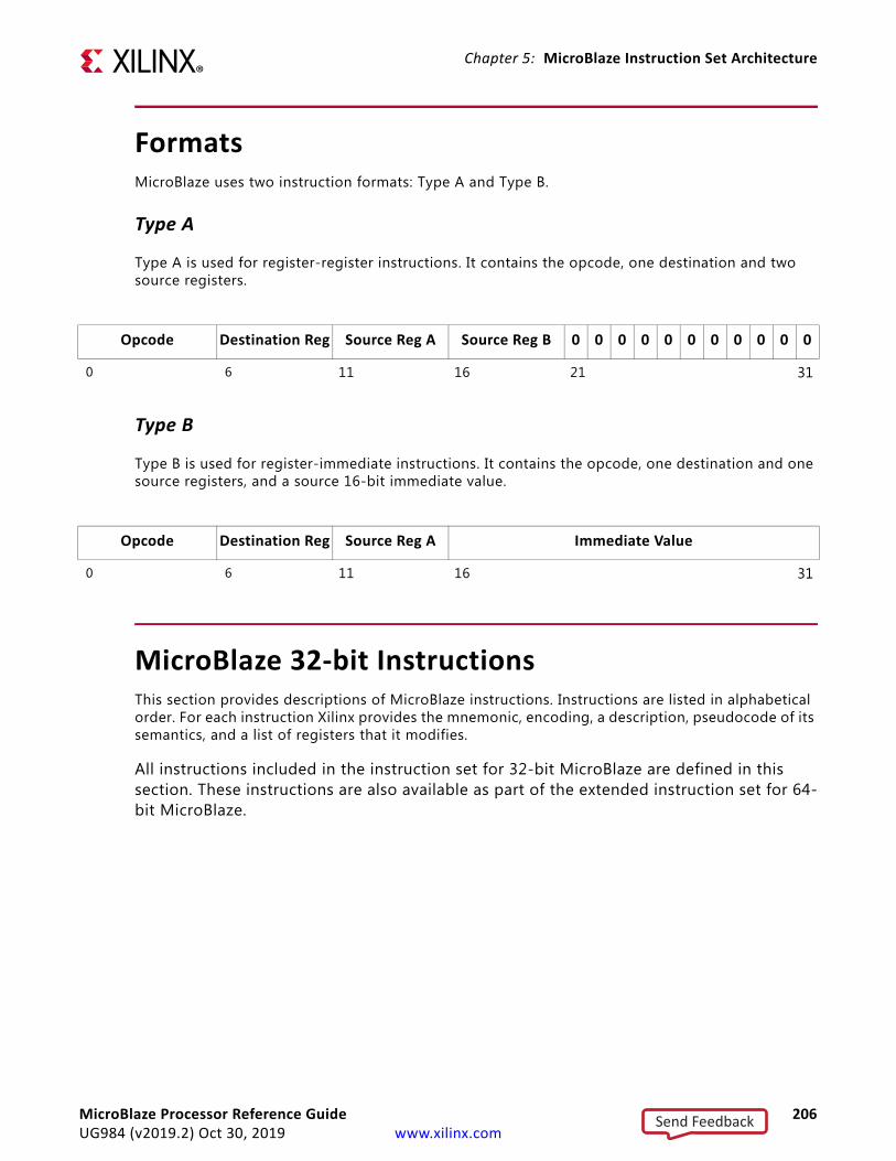
Chapter 5: MicroBlaze Instruction Set Architecture
FormatsMicroBlaze uses two instruction formats: Type A and Type B.
Type A
Type A is used for register-register instructions. It contains the opcode, one destination and two source registers.
Type B
Type B is used for register-immediate instructions. It contains the opcode, one destination and one source registers, and a source 16-bit immediate value.
MicroBlaze 32-bit InstructionsThis section provides descriptions of MicroBlaze instructions. Instructions are listed in alphabetical order. For each instruction Xilinx provides the mnemonic, encoding, a description, pseudocode of its semantics, and a list of registers that it modifies.
All instructions included in the instruction set for 32-bit MicroBlaze are defined in this section. These instructions are also available as part of the extended instruction set for 64-bit MicroBlaze.
Opcode Destination Reg Source Reg A Source Reg B 0 0 0 0 0 0 0 0 0 0 0
0 6 11 16 21 31
Opcode Destination Reg Source Reg A Immediate Value
0 6 11 16 31
MicroBlaze Processor Reference Guide 206UG984 (v2019.2) Oct 30, 2019 www.xilinx.com
Send Feedback

Chapter 5: MicroBlaze Instruction Set Architecture
add Arithmetic Add
add rD, rA, rB Add
addc rD, rA, rB Add with Carry
addk rD, rA, rB Add and Keep Carry
addkc rD, rA, rB Add with Carry and Keep Carry
0 0 0 K C 0 rD rA rB 0 0 0 0 0 0 0 0 0 0 0
0 6 11 16 21 31
DescriptionThe sum of the contents of registers rA and rB, is placed into register rD.
Bit 3 of the instruction (labeled as K in the figure) is set to one for the mnemonic addk. Bit 4 of the instruction (labeled as C in the figure) is set to one for the mnemonic addc. Both bits are set to one for the mnemonic addkc.
When an add instruction has bit 3 set (addk, addkc), the carry flag will Keep its previous value regardless of the outcome of the execution of the instruction. If bit 3 is cleared (add, addc), then the carry flag will be affected by the execution of the instruction.
When bit 4 of the instruction is set to one (addc, addkc), the content of the carry flag (MSR[C]) affects the execution of the instruction. When bit 4 is cleared (add, addk), the content of the carry flag does not affect the execution of the instruction (providing a normal addition).
Pseudocodeif C = 0 then(rD) ← (rA) + (rB)
else(rD) ← (rA) + (rB) + MSR[C]
if K = 0 thenMSR[C] ← CarryOut
Registers Altered• rD• MSR[C]
Latency1 cycle
NotesThe C bit in the instruction opcode is not the same as the carry bit in the MSR.
The “add r0, r0, r0” (= 0x00000000) instruction is never used by the compiler and usually indicates uninitialized memory. If you are using illegal instruction exceptions you can trap these instructions by setting the MicroBlaze parameter C_OPCODE_0x0_ILLEGAL=1.
MicroBlaze Processor Reference Guide 207UG984 (v2019.2) Oct 30, 2019 www.xilinx.com
Send Feedback
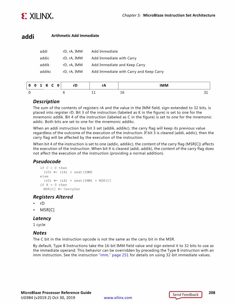
Chapter 5: MicroBlaze Instruction Set Architecture
addi Arithmetic Add Immediate
addi rD, rA, IMM Add Immediate
addic rD, rA, IMM Add Immediate with Carry
addik rD, rA, IMM Add Immediate and Keep Carry
addikc rD, rA, IMM Add Immediate with Carry and Keep Carry
0 0 1 K C 0 rD rA IMM
0 6 11 16 31
DescriptionThe sum of the contents of registers rA and the value in the IMM field, sign-extended to 32 bits, is placed into register rD. Bit 3 of the instruction (labeled as K in the figure) is set to one for the mnemonic addik. Bit 4 of the instruction (labeled as C in the figure) is set to one for the mnemonic addic. Both bits are set to one for the mnemonic addikc.
When an addi instruction has bit 3 set (addik, addikc), the carry flag will keep its previous value regardless of the outcome of the execution of the instruction. If bit 3 is cleared (addi, addic), then the carry flag will be affected by the execution of the instruction.
When bit 4 of the instruction is set to one (addic, addikc), the content of the carry flag (MSR[C]) affects the execution of the instruction. When bit 4 is cleared (addi, addik), the content of the carry flag does not affect the execution of the instruction (providing a normal addition).
Pseudocodeif C = 0 then(rD) ← (rA) + sext(IMM)
else(rD) ← (rA) + sext(IMM) + MSR[C]
if K = 0 thenMSR[C] ← CarryOut
Registers Altered• rD• MSR[C]
Latency1 cycle
NotesThe C bit in the instruction opcode is not the same as the carry bit in the MSR.
By default, Type B Instructions take the 16-bit IMM field value and sign extend it to 32 bits to use as the immediate operand. This behavior can be overridden by preceding the Type B instruction with an imm instruction. See the instruction “imm,” page 251 for details on using 32-bit immediate values.
MicroBlaze Processor Reference Guide 208UG984 (v2019.2) Oct 30, 2019 www.xilinx.com
Send Feedback

Chapter 5: MicroBlaze Instruction Set Architecture
and Logical AND
and rD, rA, rB
1 0 0 0 0 1 rD rA rB 0 0 0 0 0 0 0 0 0 0 0
0 6 11 16 21 31
DescriptionThe contents of register rA are ANDed with the contents of register rB; the result is placed into register rD.
Pseudocode(rD) ← (rA) ∧ (rB)
Registers Altered• rD
Latency1 cycle
MicroBlaze Processor Reference Guide 209UG984 (v2019.2) Oct 30, 2019 www.xilinx.com
Send Feedback

Chapter 5: MicroBlaze Instruction Set Architecture
andi Logial AND with Immediate
andi rD, rA, IMM
1 0 1 0 0 1 rD rA IMM
0 6 11 16 31
DescriptionThe contents of register rA are ANDed with the value of the IMM field, sign-extended to 32 bits; the result is placed into register rD.
Pseudocode(rD) ← (rA) ∧ sext(IMM)
Registers Altered• rD
Latency1 cycle
NoteBy default, Type B Instructions will take the 16-bit IMM field value and sign extend it to 32 bits to use as the immediate operand. This behavior can be overridden by preceding the Type B instruction with an imm instruction. See the instruction “imm” for details on using 32-bit immediate values.
MicroBlaze Processor Reference Guide 210UG984 (v2019.2) Oct 30, 2019 www.xilinx.com
Send Feedback

Chapter 5: MicroBlaze Instruction Set Architecture
andn Logical AND NOT
andn rD, rA, rB
1 0 0 0 1 1 rD rA rB 0 0 0 0 0 0 0 0 0 0 0
0 6 11 16 21 31
DescriptionThe contents of register rA are ANDed with the logical complement of the contents of register rB; the result is placed into register rD.
Pseudocode(rD) ← (rA) ∧ (rB)
Registers Altered• rD
Latency1 cycle
MicroBlaze Processor Reference Guide 211UG984 (v2019.2) Oct 30, 2019 www.xilinx.com
Send Feedback

Chapter 5: MicroBlaze Instruction Set Architecture
andni Logical AND NOT with Immediate
andni rD, rA, IMM
1 0 1 0 1 1 rD rA IMM
0 6 11 16 31
DescriptionThe IMM field is sign-extended to 32 bits. The contents of register rA are ANDed with the logical complement of the extended IMM field; the result is placed into register rD.
Pseudocode(rD) ← (rA) ∧ (sext(IMM))
Registers Altered• rD
Latency1 cycle
NoteBy default, Type B Instructions will take the 16-bit IMM field value and sign extend it to 32 bits to use as the immediate operand. This behavior can be overridden by preceding the Type B instruction with an imm instruction. See the instruction “imm” for details on using 32-bit immediate values.
MicroBlaze Processor Reference Guide 212UG984 (v2019.2) Oct 30, 2019 www.xilinx.com
Send Feedback

Chapter 5: MicroBlaze Instruction Set Architecture
beq Branch if Equal
beq rA, rB Branch if Equal
beqd rA, rB Branch if Equal with Delay
1 0 0 1 1 1 D 0 0 0 0 rA rB 0 0 0 0 0 0 0 0 0 0 0
0 6 11 16 21 31
DescriptionBranch if rA is equal to 0, to the instruction located in the offset value of rB. The target of the branch will be the instruction at address PC + rB.
The mnemonic beqd will set the D bit. The D bit determines whether there is a branch delay slot or not. If the D bit is set, it means that there is a delay slot and the instruction following the branch (that is, in the branch delay slot) is allowed to complete execution before executing the target instruction. If the D bit is not set, it means that there is no delay slot, so the instruction to be executed after the branch is the target instruction.
PseudocodeIf rA = 0 then PC ← PC + rB
else PC ← PC + 4
if D = 1 then allow following instruction to complete execution
Registers Altered• PC
Latency• 1 cycle (if branch is not taken)• 2 cycles (if branch is taken and the D bit is set)• 3 cycles (if branch is taken and the D bit is not set)
NoteA delay slot must not be used by the following: imm, branch, or break instructions. Interrupts and external hardware breaks are deferred until after the delay slot branch has been completed.
MicroBlaze Processor Reference Guide 213UG984 (v2019.2) Oct 30, 2019 www.xilinx.com
Send Feedback

Chapter 5: MicroBlaze Instruction Set Architecture
beqi Branch Immediate if Equal
beqi rA, IMM Branch Immediate if Equal
beqid rA, IMM Branch Immediate if Equal with Delay
1 0 1 1 1 1 D 0 0 0 0 rA IMM
0 6 11 16 31
DescriptionBranch if rA is equal to 0, to the instruction located in the offset value of IMM. The target of the branch will be the instruction at address PC + IMM.
The mnemonic beqid will set the D bit. The D bit determines whether there is a branch delay slot or not. If the D bit is set, it means that there is a delay slot and the instruction following the branch (that is, in the branch delay slot) is allowed to complete execution before executing the target instruction. If the D bit is not set, it means that there is no delay slot, so the instruction to be executed after the branch is the target instruction.
PseudocodeIf rA = 0 then PC ← PC + sext(IMM)
else PC ← PC + 4
if D = 1 then allow following instruction to complete execution
Registers Altered• PC
Latency• 1 cycle (if branch is not taken, or successful branch prediction occurs)• 2 cycles (if branch is taken and the D bit is set)• 3 cycles (if branch is taken and the D bit is not set, or a branch prediction mispredict
occurs with C_AREA_OPTIMIZED=0)• 7-9 cycles (if a branch prediction mispredict occurs with C_AREA_OPTIMIZED=2)
NotesBy default, Type B Instructions will take the 16-bit IMM field value and sign extend it to 32 bits to use as the immediate operand. This behavior can be overridden by preceding the Type B instruction with an imm instruction. See the instruction “imm” for details on using 32-bit immediate values.
A delay slot must not be used by the following: imm, branch, or break instructions. Interrupts and external hardware breaks are deferred until after the delay slot branch has been completed.
MicroBlaze Processor Reference Guide 214UG984 (v2019.2) Oct 30, 2019 www.xilinx.com
Send Feedback
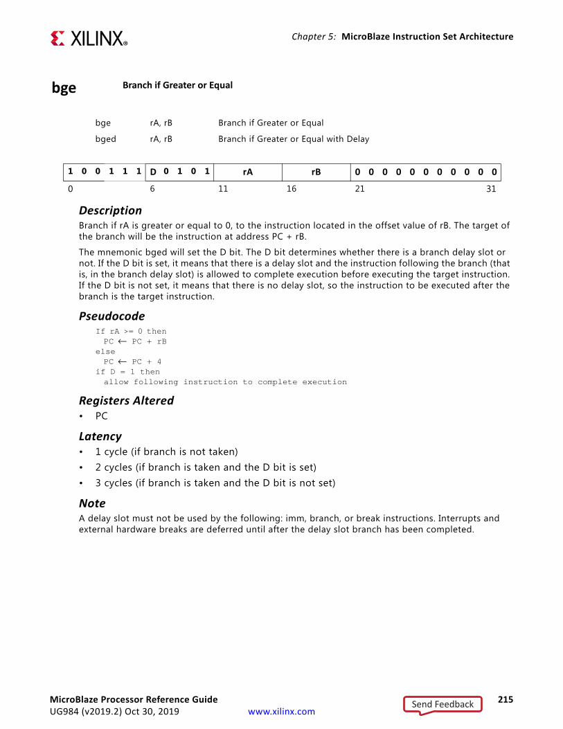
Chapter 5: MicroBlaze Instruction Set Architecture
bge Branch if Greater or Equal
bge rA, rB Branch if Greater or Equal
bged rA, rB Branch if Greater or Equal with Delay
1 0 0 1 1 1 D 0 1 0 1 rA rB 0 0 0 0 0 0 0 0 0 0 0
0 6 11 16 21 31
DescriptionBranch if rA is greater or equal to 0, to the instruction located in the offset value of rB. The target of the branch will be the instruction at address PC + rB.
The mnemonic bged will set the D bit. The D bit determines whether there is a branch delay slot or not. If the D bit is set, it means that there is a delay slot and the instruction following the branch (that is, in the branch delay slot) is allowed to complete execution before executing the target instruction. If the D bit is not set, it means that there is no delay slot, so the instruction to be executed after the branch is the target instruction.
PseudocodeIf rA >= 0 then PC ← PC + rB
else PC ← PC + 4
if D = 1 then allow following instruction to complete execution
Registers Altered• PC
Latency• 1 cycle (if branch is not taken)• 2 cycles (if branch is taken and the D bit is set)• 3 cycles (if branch is taken and the D bit is not set)
NoteA delay slot must not be used by the following: imm, branch, or break instructions. Interrupts and external hardware breaks are deferred until after the delay slot branch has been completed.
MicroBlaze Processor Reference Guide 215UG984 (v2019.2) Oct 30, 2019 www.xilinx.com
Send Feedback
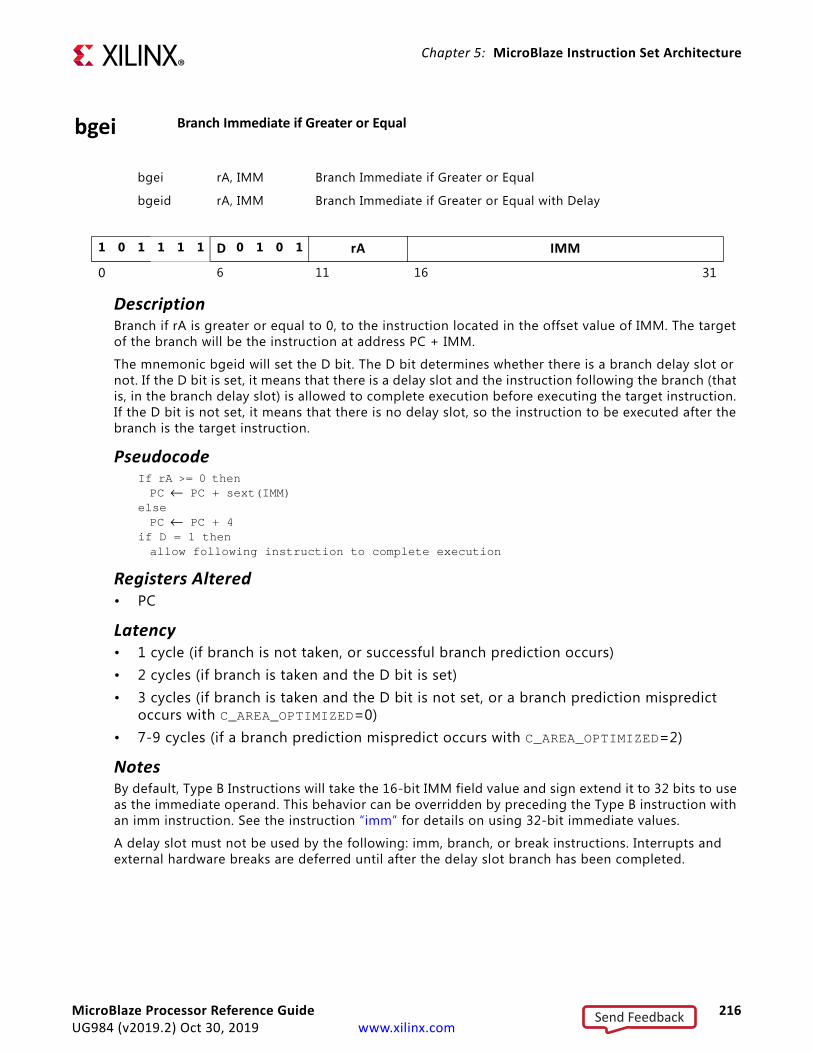
Chapter 5: MicroBlaze Instruction Set Architecture
bgei Branch Immediate if Greater or Equal
bgei rA, IMM Branch Immediate if Greater or Equal
bgeid rA, IMM Branch Immediate if Greater or Equal with Delay
1 0 1 1 1 1 D 0 1 0 1 rA IMM
0 6 11 16 31
DescriptionBranch if rA is greater or equal to 0, to the instruction located in the offset value of IMM. The target of the branch will be the instruction at address PC + IMM.
The mnemonic bgeid will set the D bit. The D bit determines whether there is a branch delay slot or not. If the D bit is set, it means that there is a delay slot and the instruction following the branch (that is, in the branch delay slot) is allowed to complete execution before executing the target instruction. If the D bit is not set, it means that there is no delay slot, so the instruction to be executed after the branch is the target instruction.
PseudocodeIf rA >= 0 then PC ← PC + sext(IMM)
else PC ← PC + 4
if D = 1 then allow following instruction to complete execution
Registers Altered• PC
Latency• 1 cycle (if branch is not taken, or successful branch prediction occurs)• 2 cycles (if branch is taken and the D bit is set)• 3 cycles (if branch is taken and the D bit is not set, or a branch prediction mispredict
occurs with C_AREA_OPTIMIZED=0)• 7-9 cycles (if a branch prediction mispredict occurs with C_AREA_OPTIMIZED=2)
NotesBy default, Type B Instructions will take the 16-bit IMM field value and sign extend it to 32 bits to use as the immediate operand. This behavior can be overridden by preceding the Type B instruction with an imm instruction. See the instruction “imm” for details on using 32-bit immediate values.
A delay slot must not be used by the following: imm, branch, or break instructions. Interrupts and external hardware breaks are deferred until after the delay slot branch has been completed.
MicroBlaze Processor Reference Guide 216UG984 (v2019.2) Oct 30, 2019 www.xilinx.com
Send Feedback

Chapter 5: MicroBlaze Instruction Set Architecture
bgt Branch if Greater Than
bgt rA, rB Branch if Greater Than
bgtd rA, rB Branch if Greater Than with Delay
1 0 0 1 1 1 D 0 1 0 0 rA rB 0 0 0 0 0 0 0 0 0 0 0
0 6 11 16 21 31
DescriptionBranch if rA is greater than 0, to the instruction located in the offset value of rB. The target of the branch will be the instruction at address PC + rB.
The mnemonic bgtd will set the D bit. The D bit determines whether there is a branch delay slot or not. If the D bit is set, it means that there is a delay slot and the instruction following the branch (that is, in the branch delay slot) is allowed to complete execution before executing the target instruction. If the D bit is not set, it means that there is no delay slot, so the instruction to be executed after the branch is the target instruction.
PseudocodeIf rA > 0 then PC ← PC + rB
else PC ← PC + 4
if D = 1 then allow following instruction to complete execution
Registers Altered• PC
Latency• 1 cycle (if branch is not taken)• 2 cycles (if branch is taken and the D bit is set)• 3 cycles (if branch is taken and the D bit is not set)
NoteA delay slot must not be used by the following: imm, branch, or break instructions. Interrupts and external hardware breaks are deferred until after the delay slot branch has been completed.
MicroBlaze Processor Reference Guide 217UG984 (v2019.2) Oct 30, 2019 www.xilinx.com
Send Feedback

Chapter 5: MicroBlaze Instruction Set Architecture
bgti Branch Immediate if Greater Than
bgti rA, IMM Branch Immediate if Greater Than
bgtid rA, IMM Branch Immediate if Greater Than with Delay
1 0 1 1 1 1 D 0 1 0 0 rA IMM
0 6 11 16 31
DescriptionBranch if rA is greater than 0, to the instruction located in the offset value of IMM. The target of the branch will be the instruction at address PC + IMM.
The mnemonic bgtid will set the D bit. The D bit determines whether there is a branch delay slot or not. If the D bit is set, it means that there is a delay slot and the instruction following the branch (that is, in the branch delay slot) is allowed to complete execution before executing the target instruction. If the D bit is not set, it means that there is no delay slot, so the instruction to be executed after the branch is the target instruction.
PseudocodeIf rA > 0 then PC ← PC + sext(IMM)
else PC ← PC + 4
if D = 1 then allow following instruction to complete execution
Registers Altered• PC
Latency• 1 cycle (if branch is not taken, or successful branch prediction occurs)• 2 cycles (if branch is taken and the D bit is set)• 3 cycles (if branch is taken and the D bit is not set, or a branch prediction mispredict
occurs with C_AREA_OPTIMIZED=0)• 7-9 cycles (if a branch prediction mispredict occurs with C_AREA_OPTIMIZED=2)
NotesBy default, Type B Instructions will take the 16-bit IMM field value and sign extend it to 32 bits to use as the immediate operand. This behavior can be overridden by preceding the Type B instruction with an imm instruction. See the instruction “imm” for details on using 32-bit immediate values.
A delay slot must not be used by the following: imm, branch, or break instructions. Interrupts and external hardware breaks are deferred until after the delay slot branch has been completed.
MicroBlaze Processor Reference Guide 218UG984 (v2019.2) Oct 30, 2019 www.xilinx.com
Send Feedback

Chapter 5: MicroBlaze Instruction Set Architecture
ble Branch if Less or Equal
ble rA, rB Branch if Less or Equal
bled rA, rB Branch if Less or Equal with Delay
1 0 0 1 1 1 D 0 0 1 1 rA rB 0 0 0 0 0 0 0 0 0 0 0
0 6 11 16 21 31
DescriptionBranch if rA is less or equal to 0, to the instruction located in the offset value of rB. The target of the branch will be the instruction at address PC + rB.
The mnemonic bled will set the D bit. The D bit determines whether there is a branch delay slot or not. If the D bit is set, it means that there is a delay slot and the instruction following the branch (that is, in the branch delay slot) is allowed to complete execution before executing the target instruction. If the D bit is not set, it means that there is no delay slot, so the instruction to be executed after the branch is the target instruction.
PseudocodeIf rA <= 0 then PC ← PC + rB
else PC ← PC + 4
if D = 1 then allow following instruction to complete execution
Registers Altered• PC
Latency• 1 cycle (if branch is not taken)• 2 cycles (if branch is taken and the D bit is set)• 3 cycles (if branch is taken and the D bit is not set)
NoteA delay slot must not be used by the following: imm, branch, or break instructions. Interrupts and external hardware breaks are deferred until after the delay slot branch has been completed.
MicroBlaze Processor Reference Guide 219UG984 (v2019.2) Oct 30, 2019 www.xilinx.com
Send Feedback
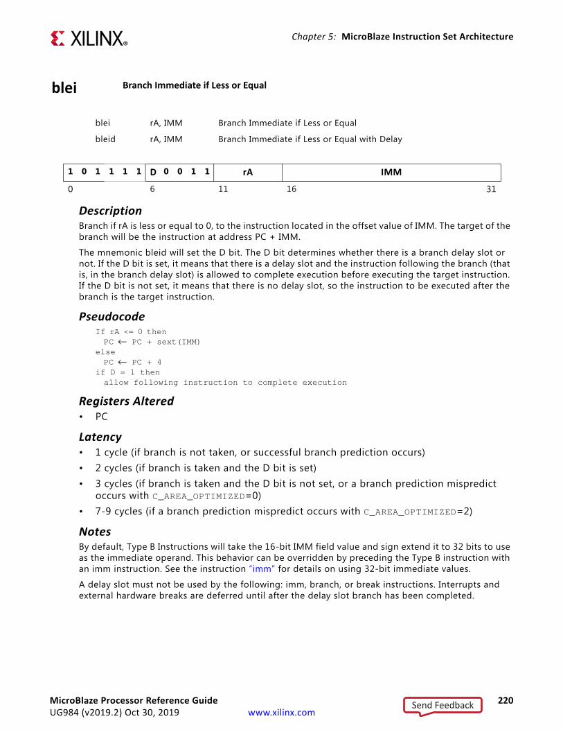
Chapter 5: MicroBlaze Instruction Set Architecture
blei Branch Immediate if Less or Equal
blei rA, IMM Branch Immediate if Less or Equal
bleid rA, IMM Branch Immediate if Less or Equal with Delay
1 0 1 1 1 1 D 0 0 1 1 rA IMM
0 6 11 16 31
DescriptionBranch if rA is less or equal to 0, to the instruction located in the offset value of IMM. The target of the branch will be the instruction at address PC + IMM.
The mnemonic bleid will set the D bit. The D bit determines whether there is a branch delay slot or not. If the D bit is set, it means that there is a delay slot and the instruction following the branch (that is, in the branch delay slot) is allowed to complete execution before executing the target instruction. If the D bit is not set, it means that there is no delay slot, so the instruction to be executed after the branch is the target instruction.
PseudocodeIf rA <= 0 then PC ← PC + sext(IMM)
else PC ← PC + 4
if D = 1 then allow following instruction to complete execution
Registers Altered• PC
Latency• 1 cycle (if branch is not taken, or successful branch prediction occurs)• 2 cycles (if branch is taken and the D bit is set)• 3 cycles (if branch is taken and the D bit is not set, or a branch prediction mispredict
occurs with C_AREA_OPTIMIZED=0)• 7-9 cycles (if a branch prediction mispredict occurs with C_AREA_OPTIMIZED=2)
NotesBy default, Type B Instructions will take the 16-bit IMM field value and sign extend it to 32 bits to use as the immediate operand. This behavior can be overridden by preceding the Type B instruction with an imm instruction. See the instruction “imm” for details on using 32-bit immediate values.
A delay slot must not be used by the following: imm, branch, or break instructions. Interrupts and external hardware breaks are deferred until after the delay slot branch has been completed.
MicroBlaze Processor Reference Guide 220UG984 (v2019.2) Oct 30, 2019 www.xilinx.com
Send Feedback

Chapter 5: MicroBlaze Instruction Set Architecture
blt Branch if Less Than
blt rA, rB Branch if Less Than
bltd rA, rB Branch if Less Than with Delay
1 0 0 1 1 1 D 0 0 1 0 rA rB 0 0 0 0 0 0 0 0 0 0 0
0 6 11 16 21 31
DescriptionBranch if rA is less than 0, to the instruction located in the offset value of rB. The target of the branch will be the instruction at address PC + rB.
The mnemonic bltd will set the D bit. The D bit determines whether there is a branch delay slot or not. If the D bit is set, it means that there is a delay slot and the instruction following the branch (that is, in the branch delay slot) is allowed to complete execution before executing the target instruction. If the D bit is not set, it means that there is no delay slot, so the instruction to be executed after the branch is the target instruction.
PseudocodeIf rA < 0 then PC ← PC + rB
else PC ← PC + 4
if D = 1 then allow following instruction to complete execution
Registers Altered• PC
Latency• 1 cycle (if branch is not taken)• 2 cycles (if branch is taken and the D bit is set)• 3 cycles (if branch is taken and the D bit is not set)
NoteA delay slot must not be used by the following: imm, branch, or break instructions. Interrupts and external hardware breaks are deferred until after the delay slot branch has been completed.
MicroBlaze Processor Reference Guide 221UG984 (v2019.2) Oct 30, 2019 www.xilinx.com
Send Feedback

Chapter 5: MicroBlaze Instruction Set Architecture
blti Branch Immediate if Less Than
blti rA, IMM Branch Immediate if Less Than
bltid rA, IMM Branch Immediate if Less Than with Delay
1 0 1 1 1 1 D 0 0 1 0 rA IMM
0 6 11 16 31
DescriptionBranch if rA is less than 0, to the instruction located in the offset value of IMM. The target of the branch will be the instruction at address PC + IMM.
The mnemonic bltid will set the D bit. The D bit determines whether there is a branch delay slot or not. If the D bit is set, it means that there is a delay slot and the instruction following the branch (that is, in the branch delay slot) is allowed to complete execution before executing the target instruction. If the D bit is not set, it means that there is no delay slot, so the instruction to be executed after the branch is the target instruction.
PseudocodeIf rA < 0 then PC ← PC + sext(IMM)
else PC ← PC + 4
if D = 1 then allow following instruction to complete execution
Registers Altered• PC
Latency• 1 cycle (if branch is not taken, or successful branch prediction occurs)• 2 cycles (if branch is taken and the D bit is set)• 3 cycles (if branch is taken and the D bit is not set, or a branch prediction mispredict
occurs with C_AREA_OPTIMIZED=0)• 7-9 cycles (if a branch prediction mispredict occurs with C_AREA_OPTIMIZED=2)
NotesBy default, Type B Instructions will take the 16-bit IMM field value and sign extend it to 32 bits to use as the immediate operand. This behavior can be overridden by preceding the Type B instruction with an imm instruction. See the instruction “imm” for details on using 32-bit immediate values.
A delay slot must not be used by the following: imm, branch, or break instructions. Interrupts and external hardware breaks are deferred until after the delay slot branch has been completed.
MicroBlaze Processor Reference Guide 222UG984 (v2019.2) Oct 30, 2019 www.xilinx.com
Send Feedback

Chapter 5: MicroBlaze Instruction Set Architecture
bne Branch if Not Equal
bne rA, rB Branch if Not Equal
bned rA, rB Branch if Not Equal with Delay
1 0 0 1 1 1 D 0 0 0 1 rA rB 0 0 0 0 0 0 0 0 0 0 0
0 6 11 16 21 31
DescriptionBranch if rA not equal to 0, to the instruction located in the offset value of rB. The target of the branch will be the instruction at address PC + rB.
The mnemonic bned will set the D bit. The D bit determines whether there is a branch delay slot or not. If the D bit is set, it means that there is a delay slot and the instruction following the branch (that is, in the branch delay slot) is allowed to complete execution before executing the target instruction. If the D bit is not set, it means that there is no delay slot, so the instruction to be executed after the branch is the target instruction.
PseudocodeIf rA ≠ 0 then PC ← PC + rB
else PC ← PC + 4
if D = 1 then allow following instruction to complete execution
Registers Altered• PC
Latency• 1 cycle (if branch is not taken)• 2 cycles (if branch is taken and the D bit is set)• 3 cycles (if branch is taken and the D bit is not set)
NoteA delay slot must not be used by the following: imm, branch, or break instructions. Interrupts and external hardware breaks are deferred until after the delay slot branch has been completed.
MicroBlaze Processor Reference Guide 223UG984 (v2019.2) Oct 30, 2019 www.xilinx.com
Send Feedback

Chapter 5: MicroBlaze Instruction Set Architecture
bnei Branch Immediate if Not Equal
bnei rA, IMM Branch Immediate if Not Equal
bneid rA, IMM Branch Immediate if Not Equal with Delay
1 0 1 1 1 1 D 0 0 0 1 rA IMM
0 6 11 16 31
DescriptionBranch if rA not equal to 0, to the instruction located in the offset value of IMM. The target of the branch will be the instruction at address PC + IMM.
The mnemonic bneid will set the D bit. The D bit determines whether there is a branch delay slot or not. If the D bit is set, it means that there is a delay slot and the instruction following the branch (that is, in the branch delay slot) is allowed to complete execution before executing the target instruction. If the D bit is not set, it means that there is no delay slot, so the instruction to be executed after the branch is the target instruction.
PseudocodeIf rA ≠ 0 then PC ← PC + sext(IMM)
else PC ← PC + 4
if D = 1 then allow following instruction to complete execution
Registers Altered• PC
Latency• 1 cycle (if branch is not taken, or successful branch prediction occurs)• 2 cycles (if branch is taken and the D bit is set)• 3 cycles (if branch is taken and the D bit is not set, or a branch prediction mispredict
occurs with C_AREA_OPTIMIZED=0)• 7-9 cycles (if a branch prediction mispredict occurs with C_AREA_OPTIMIZED=2)
NotesBy default, Type B Instructions will take the 16-bit IMM field value and sign extend it to 32 bits to use as the immediate operand. This behavior can be overridden by preceding the Type B instruction with an imm instruction. See the instruction “imm” for details on using 32-bit immediate values.
A delay slot must not be used by the following: imm, branch, or break instructions. Interrupts and external hardware breaks are deferred until after the delay slot branch has been completed.
MicroBlaze Processor Reference Guide 224UG984 (v2019.2) Oct 30, 2019 www.xilinx.com
Send Feedback

Chapter 5: MicroBlaze Instruction Set Architecture
br Unconditional Branch
br rB Branch
bra rB Branch Absolute
brd rB Branch with Delay
brad rB Branch Absolute with Delay
brld rD, rB Branch and Link with Delay
brald rD, rB Branch Absolute and Link with Delay
1 0 0 1 1 0 rD D A L 0 0 rB 0 0 0 0 0 0 0 0 0 0 0
0 6 11 16 21 31
DescriptionBranch to the instruction located at address determined by rB.
The mnemonics brld and brald will set the L bit. If the L bit is set, linking will be performed. The current value of PC will be stored in rD.
The mnemonics bra, brad and brald will set the A bit. If the A bit is set, it means that the branch is to an absolute value and the target is the value in rB, otherwise, it is a relative branch and the target will be PC + rB.
The mnemonics brd, brad, brld and brald will set the D bit. The D bit determines whether there is a branch delay slot or not. If the D bit is set, it means that there is a delay slot and the instruction following the branch (that is, in the branch delay slot) is allowed to complete execution before executing the target instruction.
If the D bit is not set, it means that there is no delay slot, so the instruction to be executed after the branch is the target instruction.
Pseudocodeif L = 1 then (rD) ← PC
if A = 1 then PC ← (rB)
else PC ← PC + (rB)
if D = 1 then allow following instruction to complete execution
Registers Altered• rD • PC
Latency• 2 cycles (if the D bit is set) • 3 cycles (if the D bit is not set)
MicroBlaze Processor Reference Guide 225UG984 (v2019.2) Oct 30, 2019 www.xilinx.com
Send Feedback
Chapter 5: MicroBlaze Instruction Set Architecture
NoteThe instructions brl and bral are not available. A delay slot must not be used by the following: imm, branch, or break instructions. Interrupts and external hardware breaks are deferred until after the delay slot branch has been completed.
With 64-bit mode, the absolute branch instructions bra, brad, and brald use the entire 64-bit register rBL, brald uses the entire 64-bit register rDL, and the instructions can be used for extended address branches.
MicroBlaze Processor Reference Guide 226UG984 (v2019.2) Oct 30, 2019 www.xilinx.com
Send Feedback

Chapter 5: MicroBlaze Instruction Set Architecture
bri Unconditional Branch Immediate
bri IMM Branch Immediate
brai IMM Branch Absolute Immediate
brid IMM Branch Immediate with Delay
braid IMM Branch Absolute Immediate with Delay
brlid rD, IMM Branch and Link Immediate with Delay
bralid rD, IMM Branch Absolute and Link Immediate with Delay
1 0 1 1 1 0 rD D A L 0 0 IMM
0 6 11 16 31
DescriptionBranch to the instruction located at address determined by IMM, sign-extended to 32 bits.
The mnemonics brlid and bralid will set the L bit. If the L bit is set, linking will be performed. The current value of PC will be stored in rD.
The mnemonics brai, braid and bralid will set the A bit. If the A bit is set, it means that the branch is to an absolute value and the target is the value in IMM, otherwise, it is a relative branch and the target will be PC + IMM.
The mnemonics brid, braid, brlid and bralid will set the D bit. The D bit determines whether there is a branch delay slot or not. If the D bit is set, it means that there is a delay slot and the instruction following the branch (that is, in the branch delay slot) is allowed to complete execution before executing the target instruction. If the D bit is not set, it means that there is no delay slot, so the instruction to be executed after the branch is the target instruction.
As a special case, when MicroBlaze is configured to use an MMU (C_USE_MMU >= 1) and “bralid rD, C_BASE_VECTORS+0x8“ is used to perform a User Vector Exception, the Machine Status Register bits User Mode and Virtual Mode are cleared.
Pseudocodeif L = 1 then (rD) ← PC
if A = 1 then PC ← sext(IMM)
else PC ← PC + sext(IMM)
if D = 1 then allow following instruction to complete execution
if D = 1 and A = 1 and L = 1 and IMM = C_BASE_VECTORS+0x8 thenMSR[UMS] ← MSR[UM]MSR[VMS] ← MSR[VM]MSR[UM] ← 0MSR[VM] ← 0
MicroBlaze Processor Reference Guide 227UG984 (v2019.2) Oct 30, 2019 www.xilinx.com
Send Feedback
Chapter 5: MicroBlaze Instruction Set Architecture
Registers Altered• rD• PC• MSR[UM], MSR[VM]
Latency• 1 cycle (if successful branch prediction occurs)• 2 cycles (if the D bit is set)• 3 cycles (if the D bit is not set, or a branch prediction mispredict occurs with
C_AREA_OPTIMIZED=0)• 7-9 cycles (if a branch prediction mispredict occurs with C_AREA_OPTIMIZED=2)
NotesThe instructions brli and brali are not available.
By default, Type B Instructions will take the 16-bit IMM field value and sign extend it to use as the immediate operand. This behavior can be overridden by preceding the Type B instruction with an imm instruction. See the instruction “imm” for details on using immediate values.
A delay slot must not be used by the following: imm, branch, or break instructions. Interrupts and external hardware breaks are deferred until after the delay slot branch has been completed.
With 64-bit mode, the absolute branch instructions brai, braid, and bralid may also be preceded by an imml instruction, bralid uses the entire 64-bit registers rDL, and the instructions can be used for extended address branches.
MicroBlaze Processor Reference Guide 228UG984 (v2019.2) Oct 30, 2019 www.xilinx.com
Send Feedback
Chapter 5: MicroBlaze Instruction Set Architecture
brk Break
brk rD, rB
1 0 0 1 1 0 rD 0 1 1 0 0 rB 0 0 0 0 0 0 0 0 0 0 0
0 6 11 16 21 31
DescriptionBranch and link to the instruction located at address value in rB. The current value of PC will be stored in rD. The BIP flag in the MSR will be set, and the reservation bit will be cleared.
When MicroBlaze is configured to use an MMU (C_USE_MMU >= 1) this instruction is privileged. This means that if the instruction is attempted in User Mode (MSR[UM] = 1) a Privileged Instruction exception occurs.
Pseudocodeif MSR[UM] = 1 thenESR[EC] ← 00111
else(rD) ← PCPC ← (rB)MSR[BIP] ← 1 Reservation ← 0
Registers Altered• rD• PC• MSR[BIP]• ESR[EC], in case a privileged instruction exception is generated
Latency• 3 cycles
NotesWith 64-bit mode, the instruction uses the entire 64-bit registers rBL and rDL, and can be used for extended address branches.
MicroBlaze Processor Reference Guide 229UG984 (v2019.2) Oct 30, 2019 www.xilinx.com
Send Feedback

Chapter 5: MicroBlaze Instruction Set Architecture
brki Break Immediate
brki rD, IMM
1 0 1 1 1 0 rD 0 1 1 0 0 IMM
0 6 11 16 31
DescriptionBranch and link to the instruction located at address value in IMM, sign-extended to 32 bits. The current value of PC will be stored in rD. The BIP flag in the MSR will be set, except in case of a Software Break, and the reservation bit will be cleared.
When MicroBlaze is configured to use an MMU (C_USE_MMU >= 1) this instruction is privileged, except as a special case when “brki rD, C_BASE_VECTORS+0x8” or “brki rD, C_BASE_VECTORS+0x18” is used to perform a Software Break. This means that, apart from the special case, if the instruction is attempted in User Mode (MSR[UM] = 1) a Privileged Instruction exception occurs.
As a special case, when MicroBlaze is configured to use an MMU (C_USE_MMU >= 1) and “brki rD, C_BASE_VECTORS+0x8” or “brki rD, C_BASE_VECTORS+0x18” is used to perform a Software Break, the Machine Status Register bits User Mode and Virtual Mode are cleared.
Pseudocodeif MSR[UM] and IMM ≠ C_BASE_VECTORS+0x8 and IMM ≠ C_BASE_VECTORS+0x18 thenESR[EC] ← 00111
else(rD) ← PCPC ← sext(IMM)if IMM ≠ 0x18 thenMSR[BIP] ← 1
Reservation ← 0 if IMM = C_BASE_VECTORS+0x8 or IMM = C_BASE_VECTORS+0x18 thenMSR[UMS] ← MSR[UM]MSR[UM] ← 0MSR[VMS] ← MSR[VM]MSR[VM] ← 0
Registers Altered• rD, unless an exception is generated, in which case the register is unchanged• PC• MSR[BIP], MSR[UM], MSR[VM]• ESR[EC], in case a privileged instruction exception is generated
Latency• 3 cycles
MicroBlaze Processor Reference Guide 230UG984 (v2019.2) Oct 30, 2019 www.xilinx.com
Send Feedback

Chapter 5: MicroBlaze Instruction Set Architecture
NotesBy default, Type B Instructions will take the 16-bit IMM field value and sign extend it to use as the immediate operand. This behavior can be overridden by preceding the Type B instruction with an imm instruction. See the instruction “imm” for details on using immediate values.
As a special case, the imm instruction does not override a Software Break “brki rD, 0x18” when C_DEBUG_ENABLED. is greater than zero, irrespective of the value of C_BASE_VECTORS, to allow Software Break after an imm instruction.
With 64-bit mode, the instruction may also be preceded by an imml instruction, uses the entire 64-bit register rDL, and can be used for extended address branches.
MicroBlaze Processor Reference Guide 231UG984 (v2019.2) Oct 30, 2019 www.xilinx.com
Send Feedback

Chapter 5: MicroBlaze Instruction Set Architecture
bs Barrel Shift
bsrl rD, rA, rB Barrel Shift Right Logical
bsra rD, rA, rB Barrel Shift Right Arithmetical
bsll rD, rA, rB Barrel Shift Left Logical
0 1 0 0 0 1 rD rA rB S T 0 0 0 0 0 0 0 0 0
0 6 11 16 21 31
DescriptionShifts the contents of register rA by the amount specified in register rB and puts the result in register rD.
The mnemonic bsll sets the S bit (Side bit). If the S bit is set, the barrel shift is done to the left. The mnemonics bsrl and bsra clear the S bit and the shift is done to the right.
The mnemonic bsra will set the T bit (Type bit). If the T bit is set, the barrel shift performed is Arithmetical. The mnemonics bsrl and bsll clear the T bit and the shift performed is Logical.
Pseudocodeif S = 1 then(rD) ← (rA) << (rB)[27:31]
elseif T = 1 thenif ((rB)[27:31]) ≠ 0 then(rD)[0:(rB)[27:31]-1] ← (rA)[0](rD)[(rB)[27:31]:31] ← (rA) >> (rB)[27:31]
else(rD) ← (rA)
else(rD) ← (rA) >> (rB)[27:31]
Registers Altered• rD
Latency• 1 cycle with C_AREA_OPTIMIZED=0 or 2
• 2 cycles with C_AREA_OPTIMIZED=1
NoteThese instructions are optional. To use them, MicroBlaze has to be configured to use barrel shift instructions (C_USE_BARREL=1).
MicroBlaze Processor Reference Guide 232UG984 (v2019.2) Oct 30, 2019 www.xilinx.com
Send Feedback
Chapter 5: MicroBlaze Instruction Set Architecture
bsi Barrel Shift Immediate
bsrli rD, rA, IMM Barrel Shift Right Logical Immediate
bsrai rD, rA, IMM Barrel Shift Right Arithmetic Immediate
bslli rD, rA, IMM Barrel Shift Left Logical Immediate
bsefi rD, rA, IMMW, IMMS Barrel Shift Extract Field Immediate
bsifi rD, rA, Width1, IMMS Barrel Shift Insert Field Immediate
1. Width = IMMW - IMMS + 1
0 1 1 0 0 1 rD rA 0 0 0 0 0 S T 0 0 0 0 IMM
0 6 11 16 21 27 31
0 1 1 0 0 1 rD rA I E 0 0 0 IMMW 0 IMMS
0 6 11 16 21 25 27 31
DescriptionThe first three instructions shift the contents of register rA by the amount specified by IMM and put the result in register rD.
Barrel Shift Extract Field extracts a bit f ield from register rA and puts the result in register rD. The bit f ield width is specif ied by IMMW and the shift amount is specif ied by IMMS. The bit f ield width must be in the range 1 - 31, and the condition IMMW + IMMS≤32 must apply.
Barrel Shift Insert Field inserts a bit field from register rA into register rD, modifying the existing value in register rD. The bit field width is defined by IMMW - IMMS + 1, and the shift amount is specified by IMMS. The condition IMMW ≥ IMMS must apply.
The mnemonic bslli sets the S bit (Side bit). If the S bit is set, the barrel shift is done to the left. The mnemonics bsrli and bsrai clear the S bit and the shift is done to the right.
The mnemonic bsrai sets the T bit (Type bit). If the T bit is set, the barrel shift performed is Arithmetical. The mnemonics bsrli and bslli clear the T bit and the shift performed is Logical.
The mnemonic bsefi sets the E bit (Extract bit). In this case the S and T bits are not used.
The mnemonic bsifi sets the I bit (Insert bit). In this case the S and T bits are not used.
MicroBlaze Processor Reference Guide 233UG984 (v2019.2) Oct 30, 2019 www.xilinx.com
Send Feedback
Chapter 5: MicroBlaze Instruction Set Architecture
Pseudocodeif E = 1 then(rD)[0:31-IMMW] ← 0 (rD)[32-IMMW:31] ← (rA) >> IMMS
else if I = 1 thenmask ← (0xffffffff << (IMMW + 1)) ⊕ (0xffffffff << IMMS)(rD) ← ((rA) << IMMS) ∧ mask) ∨ ((rD) ∧ mask)
else if S = 1 then(rD) ← (rA) << IMM
else if T = 1 thenif IMM ≠ 0 then(rD)[0:IMM-1] ← (rA)[0](rD)[IMM:31] ← (rA) >> IMM
else(rD) ← (rA)
else(rD) ← (rA) >> IMM
Registers Altered• rD
Latency• 1 cycle with C_AREA_OPTIMIZED=0 or 2• 2 cycles with C_AREA_OPTIMIZED=1
NotesThese are not Type B Instructions. There is no effect from a preceding imm instruction.
These instructions are optional. To use them, MicroBlaze has to be configured to use barrel shift instructions (C_USE_BARREL=1).
The assembler code “bsifi rD, rA, width, shift” denotes the actual bit field width, not the IMMW field, which is computed by IMMW = shift + width - 1.
MicroBlaze Processor Reference Guide 234UG984 (v2019.2) Oct 30, 2019 www.xilinx.com
Send Feedback
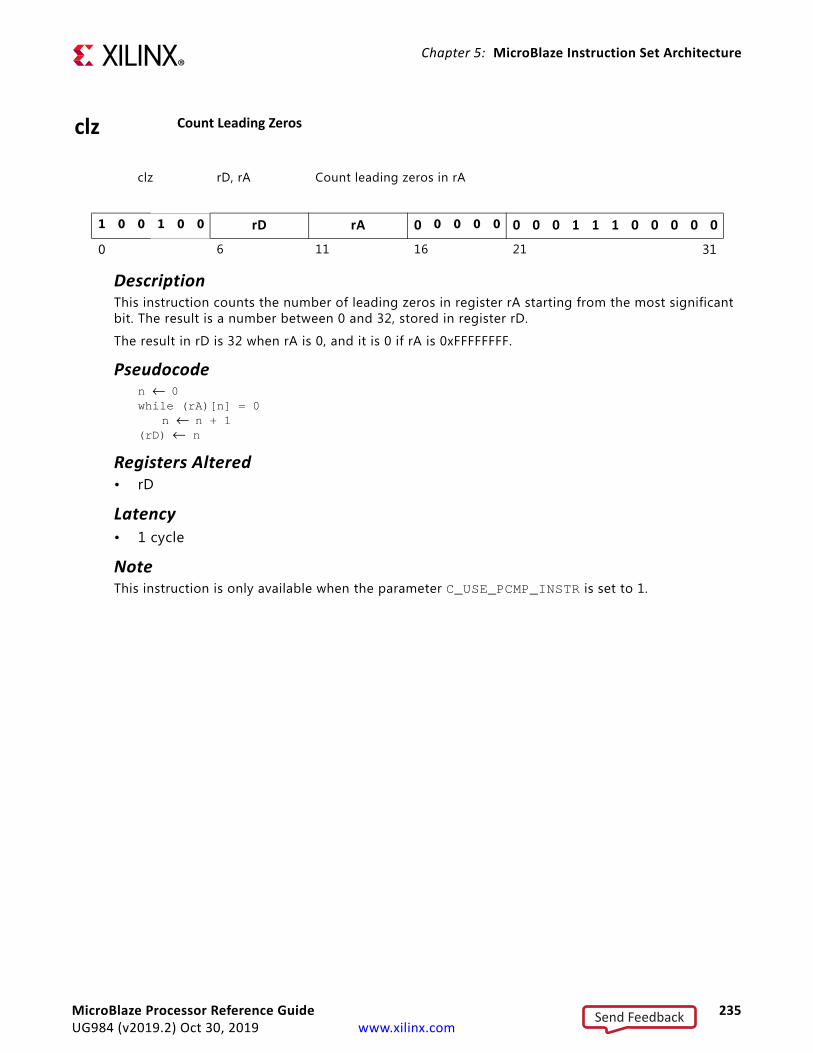
Chapter 5: MicroBlaze Instruction Set Architecture
clz Count Leading Zeros
clz rD, rA Count leading zeros in rA
1 0 0 1 0 0 rD rA 0 0 0 0 0 0 0 0 1 1 1 0 0 0 0 0
0 6 11 16 21 31
DescriptionThis instruction counts the number of leading zeros in register rA starting from the most significant bit. The result is a number between 0 and 32, stored in register rD.
The result in rD is 32 when rA is 0, and it is 0 if rA is 0xFFFFFFFF.
Pseudocoden ← 0while (rA)[n] = 0
n ← n + 1(rD) ← n
Registers Altered• rD
Latency• 1 cycle
NoteThis instruction is only available when the parameter C_USE_PCMP_INSTR is set to 1.
MicroBlaze Processor Reference Guide 235UG984 (v2019.2) Oct 30, 2019 www.xilinx.com
Send Feedback

Chapter 5: MicroBlaze Instruction Set Architecture
cmp Integer Compare
cmp rD, rA, rB compare rB with rA (signed)
cmpu rD, rA, rB compare rB with rA (unsigned)
0 0 0 1 0 1 rD rA rB 0 0 0 0 0 0 0 0 0 U 1
0 6 11 16 21 31
DescriptionThe contents of register rA are subtracted from the contents of register rB and the result is placed into register rD.
The MSB bit of rD is adjusted to shown true relation between rA and rB. If the U bit is set, rA and rB is considered unsigned values. If the U bit is clear, rA and rB is considered signed values.
Pseudocode(rD) ← (rB) + (rA) + 1(rD)(MSB) ← (rA) > (rB)
Registers Altered• rD
Latency• 1 cycle
MicroBlaze Processor Reference Guide 236UG984 (v2019.2) Oct 30, 2019 www.xilinx.com
Send Feedback

Chapter 5: MicroBlaze Instruction Set Architecture
fadd Floating-Point Arithmetic Add
fadd rD, rA, rB Add
0 1 0 1 1 0 rD rA rB 0 0 0 0 0 0 0 0 0 0 0
0 6 11 16 21 31
DescriptionThe floating-point sum of registers rA and rB, is placed into register rD.
Pseudocodeif isDnz(rA) or isDnz(rB) then(rD) ← 0xFFC00000FSR[DO] ← 1ESR[EC] ← 00110
else if isSigNaN(rA) or isSigNaN(rB)or (isPosInfinite(rA) and isNegInfinite(rB)) or(isNegInfinite(rA) and isPosInfinite(rB))) then
(rD) ← 0xFFC00000FSR[IO] ← 1ESR[EC] ← 00110
else if isQuietNaN(rA) or isQuietNaN(rB) then(rD) ← 0xFFC00000
else if isDnz((rA)+(rB)) then(rD) ← signZero((rA)+(rB))FSR[UF] ← 1ESR[EC] ← 00110
else if isNaN((rA)+(rB)) then(rD) ← signInfinite((rA)+(rB))FSR[OF] ← 1ESR[EC] ← 00110
else(rD) ← (rA) + (rB)
Registers Altered• rD, unless an FP exception is generated, in which case the register is unchanged• ESR[EC], if an FP exception is generated• FSR[IO,UF,OF,DO]
Latency• 4 cycles with C_AREA_OPTIMIZED=0• 6 cycles with C_AREA_OPTIMIZED=1• 1 cycle with C_AREA_OPTIMIZED=2
NoteThis instruction is only available when the MicroBlaze parameter C_USE_FPU is greater than 0.
MicroBlaze Processor Reference Guide 237UG984 (v2019.2) Oct 30, 2019 www.xilinx.com
Send Feedback

Chapter 5: MicroBlaze Instruction Set Architecture
frsub Reverse Floating-Point Arithmetic Subtraction
frsub rD, rA, rB Reverse subtract
0 1 0 1 1 0 rD rA rB 0 0 0 1 0 0 0 0 0 0 0
0 6 11 16 21 31
DescriptionThe floating-point value in rA is subtracted from the floating-point value in rB and the result is placed into register rD.
Pseudocodeif isDnz(rA) or isDnz(rB) then(rD) ← 0xFFC00000FSR[DO] ← 1ESR[EC] ← 00110
else if (isSigNaN(rA) or isSigNaN(rB) or (isPosInfinite(rA) and isPosInfinite(rB)) or(isNegInfinite(rA) and isNegInfinite(rB))) then
(rD) ← 0xFFC00000FSR[IO] ← 1ESR[EC] ← 00110
else if isQuietNaN(rA) or isQuietNaN(rB) then(rD) ← 0xFFC00000
else if isDnz((rB)-(rA)) then(rD) ← signZero((rB)-(rA))FSR[UF] ← 1ESR[EC] ← 00110
else if isNaN((rB)-(rA)) then(rD) ← signInfinite((rB)-(rA))FSR[OF] ← 1ESR[EC] ← 00110
else(rD) ← (rB) - (rA)
Registers Altered• rD, unless an FP exception is generated, in which case the register is unchanged• ESR[EC], if an FP exception is generated• FSR[IO,UF,OF,DO]
Latency• 4 cycles with C_AREA_OPTIMIZED=0• 6 cycles with C_AREA_OPTIMIZED=1• 1 cycle with C_AREA_OPTIMIZED=2
NoteThis instruction is only available when the MicroBlaze parameter C_USE_FPU is greater than 0.
MicroBlaze Processor Reference Guide 238UG984 (v2019.2) Oct 30, 2019 www.xilinx.com
Send Feedback

Chapter 5: MicroBlaze Instruction Set Architecture
fmul Floating-Point Arithmetic Multiplication
fmul rD, rA, rB Multiply
0 1 0 1 1 0 rD rA rB 0 0 1 0 0 0 0 0 0 0 0
0 6 11 16 21 31
DescriptionThe floating-point value in rA is multiplied with the floating-point value in rB and the result is placed into register rD.
Pseudocodeif isDnz(rA) or isDnz(rB) then(rD) ← 0xFFC00000FSR[DO] ← 1ESR[EC] ← 00110
else if isSigNaN(rA) or isSigNaN(rB) or (isZero(rA) and isInfinite(rB)) or
(isZero(rB) and isInfinite(rA)) then(rD) ← 0xFFC00000FSR[IO] ← 1ESR[EC] ← 00110
else if isQuietNaN(rA) or isQuietNaN(rB) then(rD) ← 0xFFC00000
else if isDnz((rB)*(rA)) then(rD) ← signZero((rA)*(rB))FSR[UF] ← 1ESR[EC] ← 00110
else if isNaN((rB)*(rA)) then(rD) ← signInfinite((rB)*(rA))FSR[OF] ← 1ESR[EC] ← 00110
else(rD) ← (rB) * (rA)
Registers Altered• rD, unless an FP exception is generated, in which case the register is unchanged• ESR[EC], if an FP exception is generated• FSR[IO,UF,OF,DO]
Latency• 4 cycles with C_AREA_OPTIMIZED=0• 6 cycles with C_AREA_OPTIMIZED=1• 1 cycle with C_AREA_OPTIMIZED=2
NoteThis instruction is only available when the MicroBlaze parameter C_USE_FPU is greater than 0.
MicroBlaze Processor Reference Guide 239UG984 (v2019.2) Oct 30, 2019 www.xilinx.com
Send Feedback
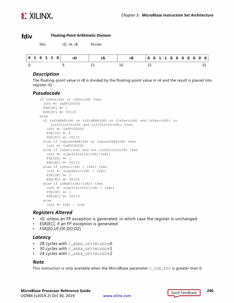
Chapter 5: MicroBlaze Instruction Set Architecture
fdiv Floating-Point Arithmetic Division
fdiv rD, rA, rB Divide
0 1 0 1 1 0 rD rA rB 0 0 1 1 0 0 0 0 0 0 0
0 6 11 16 21 31
DescriptionThe floating-point value in rB is divided by the floating-point value in rA and the result is placed into register rD.
Pseudocodeif isDnz(rA) or isDnz(rB) then(rD) ← 0xFFC00000FSR[DO] ← 1ESR[EC] ← 00110
else if isSigNaN(rA) or isSigNaN(rB) or (isZero(rA) and isZero(rB)) or
(isInfinite(rA) and isInfinite(rB)) then(rD) ← 0xFFC00000FSR[IO] ← 1ESR[EC] ← 00110
else if isQuietNaN(rA) or isQuietNaN(rB) then(rD) ← 0xFFC00000
else if isZero(rA) and not isInfinite(rB) then(rD) ← signInfinite((rB)/(rA))FSR[DZ] ← 1ESR[EC] ← 00110
else if isDnz((rB) / (rA)) then(rD) ← signZero((rB) / (rA))FSR[UF] ← 1ESR[EC] ← 00110
else if isNaN((rB)/(rA)) then(rD) ← signInfinite((rB) / (rA))FSR[OF] ← 1ESR[EC] ← 00110
else(rD) ← (rB) / (rA)
Registers Altered• rD, unless an FP exception is generated, in which case the register is unchanged• ESR[EC], if an FP exception is generated• FSR[IO,UF,OF,DO,DZ]
Latency• 28 cycles with C_AREA_OPTIMIZED=0• 30 cycles with C_AREA_OPTIMIZED=1• 24 cycles with C_AREA_OPTIMIZED=2
NoteThis instruction is only available when the MicroBlaze parameter C_USE_FPU is greater than 0.
MicroBlaze Processor Reference Guide 240UG984 (v2019.2) Oct 30, 2019 www.xilinx.com
Send Feedback

Chapter 5: MicroBlaze Instruction Set Architecture
fcmp Floating-Point Number Comparison
fcmp.un rD, rA, rB Unordered floating-point comparison
fcmp.lt rD, rA, rB Less-than floating-point comparison
fcmp.eq rD, rA, rB Equal floating-point comparison
fcmp.le rD, rA, rB Less-or-Equal floating-point comparison
fcmp.gt rD, rA, rB Greater-than floating-point comparison
fcmp.ne rD, rA, rB Not-Equal floating-point comparison
fcmp.ge rD, rA, rB Greater-or-Equal floating-point comparison
0 1 0 1 1 0 rD rA rB 0 1 0 0 OpSel 0 0 0 0
0 6 11 16 21 25 28 31
DescriptionThe floating-point value in rB is compared with the floating-point value in rA and the comparison result is placed into register rD. The OpSel field in the instruction code determines the type of comparison performed.
Pseudocodeif isDnz(rA) or isDnz(rB) then(rD) ← 0FSR[DO] ← 1ESR[EC] ← 00110
else{read out behavior from Table 5-3}
Registers Altered• rD, unless an FP exception is generated, in which case the register is unchanged• ESR[EC], if an FP exception is generated• FSR[IO,DO]
Latency• 1 cycle with C_AREA_OPTIMIZED=0 or 2• 3 cycles with C_AREA_OPTIMIZED=1
NoteThese instructions are only available when the MicroBlaze parameter C_USE_FPU is greater than 0.
Table 5-3 lists the floating-point comparison operations.
MicroBlaze Processor Reference Guide 241UG984 (v2019.2) Oct 30, 2019 www.xilinx.com
Send Feedback

Chapter 5: MicroBlaze Instruction Set Architecture
Table 5-3: Floating-Point Comparison Operation
Comparison Type Operand Relationship
Description OpSel (rB) > (rA) (rB) < (rA) (rB) = (rA) isSigNaN(rA) or isSigNaN(rB)
isQuietNaN(rA) or isQuietNaN(rB)
Unordered 000 (rD) ← 0 (rD) ← 0 (rD) ← 0 (rD) ← 1FSR[IO] ← 1ESR[EC] ← 00110
(rD) ← 1
Less-than 001 (rD) ← 0 (rD) ← 1 (rD) ← 0 (rD) ← 0FSR[IO] ← 1ESR[EC] ← 00110
(rD) ← 0FSR[IO] ← 1ESR[EC] ← 00110
Equal 010 (rD) ← 0 (rD) ← 0 (rD) ← 1 (rD) ← 0 FSR[IO] ← 1ESR[EC] ← 00110
(rD) ← 0
Less-or-equal 011 (rD) ← 0 (rD) ← 1 (rD) ← 1 (rD) ← 0FSR[IO] ← 1ESR[EC] ← 00110
(rD) ← 0FSR[IO] ← 1ESR[EC] ← 00110
Greater-than 100 (rD) ← 1 (rD) ← 0 (rD) ← 0 (rD) ← 0FSR[IO] ← 1ESR[EC] ← 00110
(rD) ← 0FSR[IO] ← 1ESR[EC] ← 00110
Not-equal 101 (rD) ← 1 (rD) ← 1 (rD) ← 0 (rD) ← 1 FSR[IO] ← 1ESR[EC] ← 00110
(rD) ← 1
Greater-or-equal 110 (rD) ← 1 (rD) ← 0 (rD) ← 1 (rD) ← 0FSR[IO] ← 1ESR[EC] ← 00110
(rD) ← 0FSR[IO] ← 1ESR[EC] ← 00110
MicroBlaze Processor Reference Guide 242UG984 (v2019.2) Oct 30, 2019 www.xilinx.com
Send Feedback
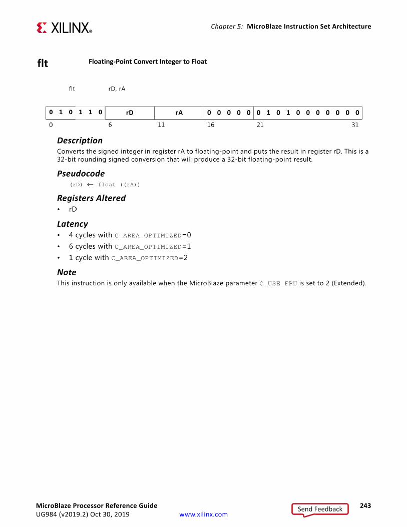
Chapter 5: MicroBlaze Instruction Set Architecture
flt Floating-Point Convert Integer to Float
flt rD, rA
0 1 0 1 1 0 rD rA 0 0 0 0 0 0 1 0 1 0 0 0 0 0 0 0
0 6 11 16 21 31
DescriptionConverts the signed integer in register rA to floating-point and puts the result in register rD. This is a 32-bit rounding signed conversion that will produce a 32-bit floating-point result.
Pseudocode(rD) ← float ((rA))
Registers Altered• rD
Latency• 4 cycles with C_AREA_OPTIMIZED=0• 6 cycles with C_AREA_OPTIMIZED=1• 1 cycle with C_AREA_OPTIMIZED=2
NoteThis instruction is only available when the MicroBlaze parameter C_USE_FPU is set to 2 (Extended).
MicroBlaze Processor Reference Guide 243UG984 (v2019.2) Oct 30, 2019 www.xilinx.com
Send Feedback

Chapter 5: MicroBlaze Instruction Set Architecture
fint Floating-Point Convert Float to Integer
fint rD, rA
0 1 0 1 1 0 rD rA 0 0 0 0 0 0 1 1 0 0 0 0 0 0 0 0
0 6 11 16 21 31
DescriptionConverts the floating-point number in register rA to a signed integer and puts the result in register rD. This is a 32-bit signed conversion that will produce a 32-bit integer result.
Pseudocodeif isDnz(rA) then(rD) ← 0xFFC00000FSR[DO] ← 1ESR[EC] ← 00110
else if isNaN(rA) then(rD) ← 0xFFC00000FSR[IO] ← 1ESR[EC] ← 00110
else if isInf(rA) or (rA) < -231 or (rA) > 231 - 1 then(rD) ← 0xFFC00000FSR[IO] ← 1ESR[EC] ← 00110
else(rD) ← int ((rA))
Registers Altered• rD, unless an FP exception is generated, in which case the register is unchanged• ESR[EC], if an FP exception is generated• FSR[IO,DO]
Latency• 5 cycles with C_AREA_OPTIMIZED=0• 7 cycles with C_AREA_OPTIMIZED=1• 2 cycles with C_AREA_OPTIMIZED=2
NoteThis instruction is only available when the MicroBlaze parameter C_USE_FPU is set to 2 (Extended).
MicroBlaze Processor Reference Guide 244UG984 (v2019.2) Oct 30, 2019 www.xilinx.com
Send Feedback
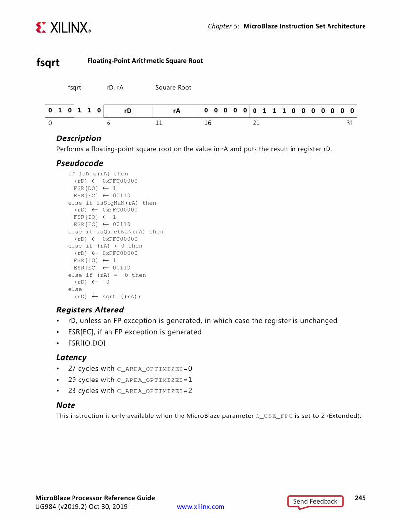
Chapter 5: MicroBlaze Instruction Set Architecture
fsqrt Floating-Point Arithmetic Square Root
fsqrt rD, rA Square Root
0 1 0 1 1 0 rD rA 0 0 0 0 0 0 1 1 1 0 0 0 0 0 0 0
0 6 11 16 21 31
DescriptionPerforms a floating-point square root on the value in rA and puts the result in register rD.
Pseudocodeif isDnz(rA) then(rD) ← 0xFFC00000FSR[DO] ← 1ESR[EC] ← 00110
else if isSigNaN(rA) then(rD) ← 0xFFC00000FSR[IO] ← 1ESR[EC] ← 00110
else if isQuietNaN(rA) then(rD) ← 0xFFC00000
else if (rA) < 0 then(rD) ← 0xFFC00000FSR[IO] ← 1ESR[EC] ← 00110
else if (rA) = -0 then(rD) ← -0
else(rD) ← sqrt ((rA))
Registers Altered• rD, unless an FP exception is generated, in which case the register is unchanged• ESR[EC], if an FP exception is generated• FSR[IO,DO]
Latency• 27 cycles with C_AREA_OPTIMIZED=0• 29 cycles with C_AREA_OPTIMIZED=1• 23 cycles with C_AREA_OPTIMIZED=2
NoteThis instruction is only available when the MicroBlaze parameter C_USE_FPU is set to 2 (Extended).
MicroBlaze Processor Reference Guide 245UG984 (v2019.2) Oct 30, 2019 www.xilinx.com
Send Feedback
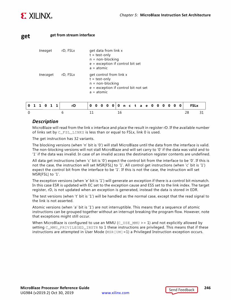
Chapter 5: MicroBlaze Instruction Set Architecture
get get from stream interface
tneaget rD, FSLx get data from link x t = test-only n = non-blocking e = exception if control bit set a = atomic
tnecaget rD, FSLx get control from link x t = test-only n = non-blocking e = exception if control bit not set a = atomic
0 1 1 0 1 1 rD 0 0 0 0 0 0 n c t a e 0 0 0 0 0 0 FSLx
0 6 11 16 28 31
DescriptionMicroBlaze will read from the link x interface and place the result in register rD. If the available number of links set by C_FSL_LINKS is less than or equal to FSLx, link 0 is used.
The get instruction has 32 variants.
The blocking versions (when ‘n’ bit is ‘0’) will stall MicroBlaze until the data from the interface is valid. The non-blocking versions will not stall MicroBlaze and will set carry to ‘0’ if the data was valid and to ‘1’ if the data was invalid. In case of an invalid access the destination register contents are undefined.
All data get instructions (when ‘c’ bit is ‘0’) expect the control bit from the interface to be ‘0’. If this is not the case, the instruction will set MSR[FSL] to ‘1’. All control get instructions (when ‘c’ bit is ‘1’) expect the control bit from the interface to be ‘1’. If this is not the case, the instruction will set MSR[FSL] to ‘1’.
The exception versions (when ‘e’ bit is ‘1’) will generate an exception if there is a control bit mismatch. In this case ESR is updated with EC set to the exception cause and ESS set to the link index. The target register, rD, is not updated when an exception is generated, instead the data is stored in EDR.
The test versions (when ‘t’ bit is ‘1’) will be handled as the normal case, except that the read signal to the link is not asserted.
Atomic versions (when ‘a’ bit is ‘1’) are not interruptible. This means that a sequence of atomic instructions can be grouped together without an interrupt breaking the program flow. However, note that exceptions might still occur.
When MicroBlaze is configured to use an MMU (C_USE_MMU >= 1) and not explicitly allowed by setting C_MMU_PRIVILEGED_INSTR to 1 these instructions are privileged. This means that if these instructions are attempted in User Mode (MSR[UM]=1) a Privileged Instruction exception occurs.
MicroBlaze Processor Reference Guide 246UG984 (v2019.2) Oct 30, 2019 www.xilinx.com
Send Feedback
Chapter 5: MicroBlaze Instruction Set Architecture
Pseudocodeif MSR[UM] = 1 thenESR[EC] ← 00111
elsex ← FSLxif x >= C_FSL_LINKS thenx ← 0
(rD) ← Sx_AXIS_TDATAif (n = 1) thenMSR[Carry] ← Sx_AXIS_TVALID
if Sx_AXIS_TLAST ≠ c and Sx_AXIS_TVALID thenMSR[FSL] ← 1 if (e = 1) thenESR[EC] ← 00000ESR[ESS]← instruction bits [28:31]EDR ← Sx_AXIS_TDATA
Registers Altered• rD, unless an exception is generated, in which case the register is unchanged• MSR[FSL]• MSR[Carry]• ESR[EC], in case a stream exception or a privileged instruction exception is generated• ESR[ESS], in case a stream exception is generated• EDR, in case a stream exception is generated
Latency• 1 cycle with C_AREA_OPTIMIZED=0 or 2• 2 cycles with C_AREA_OPTIMIZED=1The blocking versions of this instruction will stall the pipeline of MicroBlaze until the instruction can be completed. Interrupts are served when the parameter C_USE_EXTENDED_FSL_INSTR is set to 1, and the instruction is not atomic.
NotesTo refer to an FSLx interface in assembly language, use rfsl0, rfsl1, ... rfsl15.
The blocking versions of this instruction should not be placed in a delay slot when the parameter C_USE_EXTENDED_FSL_INSTR is set to 1, since this prevents interrupts from being served.
For non-blocking versions, an rsubc instruction can be used to decrement an index variable.
The ‘e’ bit does not have any effect unless C_FSL_EXCEPTION is set to 1.
These instructions are only available when the MicroBlaze parameter C_FSL_LINKS is greater than 0.
The extended instructions (exception, test and atomic versions) are only available when the MicroBlaze parameter C_USE_EXTENDED_FSL_INSTR is set to 1.
It is not recommended to allow these instructions in user mode, unless absolutely necessary for performance reasons, since that removes all hardware protection preventing incorrect use of a link.
MicroBlaze Processor Reference Guide 247UG984 (v2019.2) Oct 30, 2019 www.xilinx.com
Send Feedback

Chapter 5: MicroBlaze Instruction Set Architecture
getd get from stream interface dynamic
tneagetd rD, rB get data from link rB[28:31] t = test-only n = non-blocking e = exception if control bit set a = atomic
tnecagetd rD, rB get control from link rB[28:31] t = test-only n = non-blocking e = exception if control bit not set a = atomic
0 1 0 0 1 1 rD 0 0 0 0 0 rB 0 n c t a e 0 0 0 0 0
0 6 11 16 21 31
DescriptionMicroBlaze will read from the interface defined by the four least significant bits in rB and place the result in register rD. If the available number of links set by C_FSL_LINKS is less than or equal to the four least significant bits in rB, link 0 is used.
The getd instruction has 32 variants.
The blocking versions (when ‘n’ bit is ‘0’) will stall MicroBlaze until the data from the interface is valid. The non-blocking versions will not stall MicroBlaze and will set carry to ‘0’ if the data was valid and to ‘1’ if the data was invalid. In case of an invalid access the destination register contents are undefined.
All data get instructions (when ‘c’ bit is ‘0’) expect the control bit from the interface to be ‘0’. If this is not the case, the instruction will set MSR[FSL] to ‘1’. All control get instructions (when ‘c’ bit is ‘1’) expect the control bit from the interface to be ‘1’. If this is not the case, the instruction will set MSR[FSL] to ‘1’.
The exception versions (when ‘e’ bit is ‘1’) will generate an exception if there is a control bit mismatch. In this case ESR is updated with EC set to the exception cause and ESS set to the link index. The target register, rD, is not updated when an exception is generated, instead the data is stored in EDR.
The test versions (when ‘t’ bit is ‘1’) will be handled as the normal case, except that the read signal to the link is not asserted.
Atomic versions (when ‘a’ bit is ‘1’) are not interruptible. This means that a sequence of atomic instructions can be grouped together without an interrupt breaking the program flow. However, note that exceptions might still occur.
When MicroBlaze is configured to use an MMU (C_USE_MMU >= 1) and not explicitly allowed by setting C_MMU_PRIVILEGED_INSTR to 1 these instructions are privileged. This means that if these instructions are attempted in User Mode (MSR[UM] = 1) a Privileged Instruction exception occurs.
MicroBlaze Processor Reference Guide 248UG984 (v2019.2) Oct 30, 2019 www.xilinx.com
Send Feedback

Chapter 5: MicroBlaze Instruction Set Architecture
Pseudocodeif MSR[UM] = 1 thenESR[EC] ← 00111
elsex ← rB[28:31]if x >= C_FSL_LINKS thenx ← 0
(rD) ← Sx_AXIS_TDATAif (n = 1) thenMSR[Carry] ← Sx_AXIS_TVALID
if Sx_AXIS_TLAST ≠ c and Sx_AXIS_TVALID thenMSR[FSL] ← 1 if (e = 1) thenESR[EC] ← 00000ESR[ESS]← rB[28:31]EDR ← Sx_AXIS_TDATA
Registers Altered• rD, unless an exception is generated, in which case the register is unchanged• MSR[FSL]• MSR[Carry]• ESR[EC], in case a stream exception or a privileged instruction exception is generated• ESR[ESS], in case a stream exception is generated• EDR, in case a stream exception is generated
Latency• 1 cycle with C_AREA_OPTIMIZED=0 or 2• 2 cycles with C_AREA_OPTIMIZED=1The blocking versions of this instruction will stall the pipeline of MicroBlaze until the instruction can be completed. Interrupts are served unless the instruction is atomic, which ensures that the instruction cannot be interrupted.
NotesThe blocking versions of this instruction should not be placed in a delay slot, since this prevents interrupts from being served.
For non-blocking versions, an rsubc instruction can be used to decrement an index variable.
The ‘e’ bit does not have any effect unless C_FSL_EXCEPTION is set to 1.
These instructions are only available when the MicroBlaze parameter C_FSL_LINKS is greater than 0 and the parameter C_USE_EXTENDED_FSL_INSTR is set to 1.
It is not recommended to allow these instructions in user mode, unless absolutely necessary for performance reasons, since that removes all hardware protection preventing incorrect use of a link.
MicroBlaze Processor Reference Guide 249UG984 (v2019.2) Oct 30, 2019 www.xilinx.com
Send Feedback

Chapter 5: MicroBlaze Instruction Set Architecture
idiv Integer Divide
idiv rD, rA, rB divide rB by rA (signed)
idivu rD, rA, rB divide rB by rA (unsigned)
0 1 0 0 1 0 rD rA rB 0 0 0 0 0 0 0 0 0 U 0
0 6 11 16 21 31
DescriptionThe contents of register rB are divided by the contents of register rA and the result is placed into register rD.
If the U bit is set, rA and rB are considered unsigned values. If the U bit is clear, rA and rB are considered signed values.
If the value of rA is 0 (divide by zero), the DZO bit in MSR will be set and the value in rD will be 0, unless an exception is generated.
If the U bit is clear, the value of rA is -1, and the value of rB is -2147483648 (divide overflow), the DZO bit in MSR will be set and the value in rD will be -2147483648, unless an exception is generated.
Pseudocodeif (rA) = 0 then(rD) <- 0MSR[DZO] <- 1ESR[EC] <- 00101 ESR[DEC] <- 0
else if U = 0 and (rA) = -1 and (rB) = -2147483648 then(rD) <- -2147483648MSR[DZO] <- 1ESR[EC] <- 00101 ESR[DEC] <- 1
else(rD) ← (rB) / (rA)
Registers Altered• rD, unless a divide exception is generated, in which case the register is unchanged• MSR[DZO], if divide by zero or divide overflow occurs• ESR[EC], if divide by zero or divide overflow occurs
Latency• 1 cycle if (rA) = 0, otherwise 34 cycles with C_AREA_OPTIMIZED=0• 1 cycle if (rA) = 0, otherwise 35 cycles with C_AREA_OPTIMIZED=1• 1 cycle if (rA) = 0, otherwise 30 cycles with C_AREA_OPTIMIZED=2
NoteThis instruction is only valid if MicroBlaze is configured to use a hardware divider (C_USE_DIV = 1).
MicroBlaze Processor Reference Guide 250UG984 (v2019.2) Oct 30, 2019 www.xilinx.com
Send Feedback
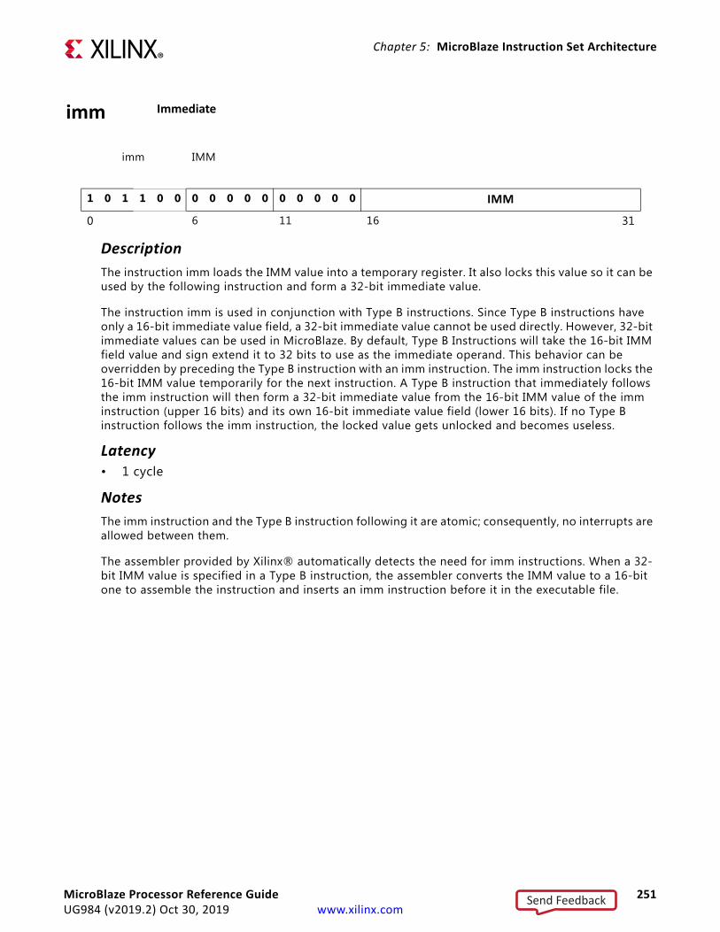
Chapter 5: MicroBlaze Instruction Set Architecture
imm Immediate
imm IMM
1 0 1 1 0 0 0 0 0 0 0 0 0 0 0 0 IMM
0 6 11 16 31
DescriptionThe instruction imm loads the IMM value into a temporary register. It also locks this value so it can be used by the following instruction and form a 32-bit immediate value.
The instruction imm is used in conjunction with Type B instructions. Since Type B instructions have only a 16-bit immediate value field, a 32-bit immediate value cannot be used directly. However, 32-bit immediate values can be used in MicroBlaze. By default, Type B Instructions will take the 16-bit IMM field value and sign extend it to 32 bits to use as the immediate operand. This behavior can be overridden by preceding the Type B instruction with an imm instruction. The imm instruction locks the 16-bit IMM value temporarily for the next instruction. A Type B instruction that immediately follows the imm instruction will then form a 32-bit immediate value from the 16-bit IMM value of the imm instruction (upper 16 bits) and its own 16-bit immediate value field (lower 16 bits). If no Type B instruction follows the imm instruction, the locked value gets unlocked and becomes useless.
Latency• 1 cycle
NotesThe imm instruction and the Type B instruction following it are atomic; consequently, no interrupts are allowed between them.
The assembler provided by Xilinx® automatically detects the need for imm instructions. When a 32-bit IMM value is specified in a Type B instruction, the assembler converts the IMM value to a 16-bit one to assemble the instruction and inserts an imm instruction before it in the executable file.
MicroBlaze Processor Reference Guide 251UG984 (v2019.2) Oct 30, 2019 www.xilinx.com
Send Feedback
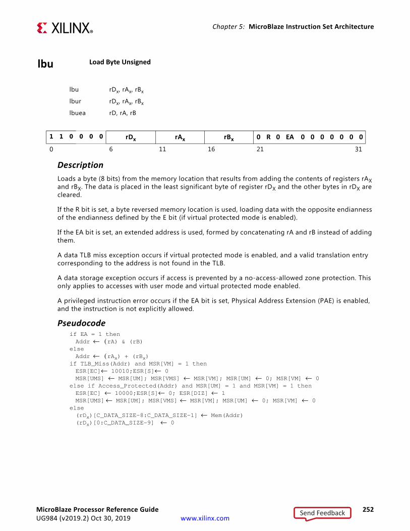
Chapter 5: MicroBlaze Instruction Set Architecture
lbu Load Byte Unsigned
lbu rDx, rAx, rBx
lbur rDx, rAx, rBx
lbuea rD, rA, rB
1 1 0 0 0 0 rDx rAx rBx 0 R 0 EA 0 0 0 0 0 0 0
0 6 11 16 21 31
DescriptionLoads a byte (8 bits) from the memory location that results from adding the contents of registers rAX and rBX. The data is placed in the least significant byte of register rDX and the other bytes in rDX are cleared.
If the R bit is set, a byte reversed memory location is used, loading data with the opposite endianness of the endianness defined by the E bit (if virtual protected mode is enabled).
If the EA bit is set, an extended address is used, formed by concatenating rA and rB instead of adding them.
A data TLB miss exception occurs if virtual protected mode is enabled, and a valid translation entry corresponding to the address is not found in the TLB.
A data storage exception occurs if access is prevented by a no-access-allowed zone protection. This only applies to accesses with user mode and virtual protected mode enabled.
A privileged instruction error occurs if the EA bit is set, Physical Address Extension (PAE) is enabled, and the instruction is not explicitly allowed.
Pseudocodeif EA = 1 thenAddr ← (rA) & (rB)
elseAddr ← (rAx) + (rBx)
if TLB_Miss(Addr) and MSR[VM] = 1 thenESR[EC]← 10010;ESR[S]← 0MSR[UMS] ← MSR[UM]; MSR[VMS] ← MSR[VM]; MSR[UM] ← 0; MSR[VM] ← 0
else if Access_Protected(Addr) and MSR[UM] = 1 and MSR[VM] = 1 thenESR[EC] ← 10000;ESR[S]← 0; ESR[DIZ] ← 1MSR[UMS]← MSR[UM]; MSR[VMS] ← MSR[VM]; MSR[UM] ← 0; MSR[VM] ← 0
else (rDx)[C_DATA_SIZE-8:C_DATA_SIZE-1] ← Mem(Addr) (rDx)[0:C_DATA_SIZE-9] ← 0
MicroBlaze Processor Reference Guide 252UG984 (v2019.2) Oct 30, 2019 www.xilinx.com
Send Feedback
Chapter 5: MicroBlaze Instruction Set Architecture
Registers Altered• rDX, unless an exception is generated, in which case the register is unchanged
• MSR[UM], MSR[VM], MSR[UMS], MSR[VMS], if an exception is generated
• ESR[EC], ESR[S], if an exception is generated
• ESR[DIZ], if a data storage exception is generated
Latency• 1 cycle with C_AREA_OPTIMIZED=0 or 2• 2 cycles with C_AREA_OPTIMIZED=1
NotesThe byte reversed instruction is only valid if MicroBlaze is configured to use reorder instructions (C_USE_REORDER_INSTR = 1).
The extended address instruction is only valid if MicroBlaze is configured to use extended address (C_ADDR_SIZE > 32) and is using 32-bit mode (C_DATA_SIZE = 32).
MicroBlaze Processor Reference Guide 253UG984 (v2019.2) Oct 30, 2019 www.xilinx.com
Send Feedback
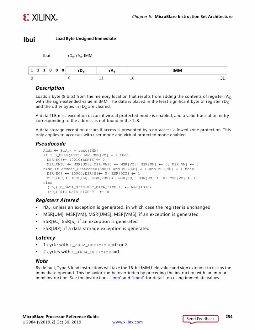
Chapter 5: MicroBlaze Instruction Set Architecture
lbui Load Byte Unsigned Immediate
lbui rDx, rAx, IMM
1 1 1 0 0 0 rDX rAX IMM
0 6 11 16 31
DescriptionLoads a byte (8 bits) from the memory location that results from adding the contents of register rAX with the sign-extended value in IMM. The data is placed in the least significant byte of register rDX and the other bytes in rDX are cleared.
A data TLB miss exception occurs if virtual protected mode is enabled, and a valid translation entry corresponding to the address is not found in the TLB.
A data storage exception occurs if access is prevented by a no-access-allowed zone protection. This only applies to accesses with user mode and virtual protected mode enabled.
PseudocodeAddr ← (rAx) + sext(IMM) if TLB_Miss(Addr) and MSR[VM] = 1 thenESR[EC]← 10010;ESR[S]← 0MSR[UMS] ← MSR[UM]; MSR[VMS] ← MSR[VM]; MSR[UM] ← 0; MSR[VM] ← 0
else if Access_Protected(Addr) and MSR[UM] = 1 and MSR[VM] = 1 thenESR[EC] ← 10000;ESR[S]← 0; ESR[DIZ] ← 1MSR[UMS]← MSR[UM]; MSR[VMS] ← MSR[VM]; MSR[UM] ← 0; MSR[VM] ← 0
else (rDx)[C_DATA_SIZE-8:C_DATA_SIZE-1] ← Mem(Addr) (rDx)[0:C_DATA_SIZE-9] ← 0
Registers Altered• rDX, unless an exception is generated, in which case the register is unchanged• MSR[UM], MSR[VM], MSR[UMS], MSR[VMS], if an exception is generated• ESR[EC], ESR[S], if an exception is generated• ESR[DIZ], if a data storage exception is generated
Latency• 1 cycle with C_AREA_OPTIMIZED=0 or 2• 2 cycles with C_AREA_OPTIMIZED=1
NoteBy default, Type B load instructions will take the 16-bit IMM field value and sign extend it to use as the immediate operand. This behavior can be overridden by preceding the instruction with an imm or imml instruction. See the instructions “imm” and “imml” for details on using immediate values.
MicroBlaze Processor Reference Guide 254UG984 (v2019.2) Oct 30, 2019 www.xilinx.com
Send Feedback

Chapter 5: MicroBlaze Instruction Set Architecture
lhu Load Halfword Unsigned
lhu rDx, rAx, rBx
lhur rDx, rAx, rBx
lhuea rD, rA, rB
1 1 0 0 0 1 rDX rAX rBX 0 R 0 EA 0 0 0 0 0 0 0
0 6 11 16 21 31
DescriptionLoads a halfword (16 bits) from the halfword aligned memory location that results from adding the contents of registers rAX and rBX. The data is placed in the least significant halfword of register rDX and the other halfwords in rDX is cleared.
If the R bit is set, a halfword reversed memory location is used and the two bytes in the halfword are reversed, loading data with the opposite endianness of the endianness defined by the E bit (if virtual protected mode is enabled).
If the EA bit is set, an extended address is used, formed by concatenating rA and rB instead of adding them.
A data TLB miss exception occurs if virtual protected mode is enabled, and a valid translation entry corresponding to the address is not found in the TLB.
A data storage exception occurs if access is prevented by a no-access-allowed zone protection. This only applies to accesses with user mode and virtual protected mode enabled.
An unaligned data access exception occurs if the least significant bit in the address is not zero.
A privileged instruction error occurs if the EA bit is set, Physical Address Extension (PAE) is enabled, and the instruction is not explicitly allowed.
MicroBlaze Processor Reference Guide 255UG984 (v2019.2) Oct 30, 2019 www.xilinx.com
Send Feedback
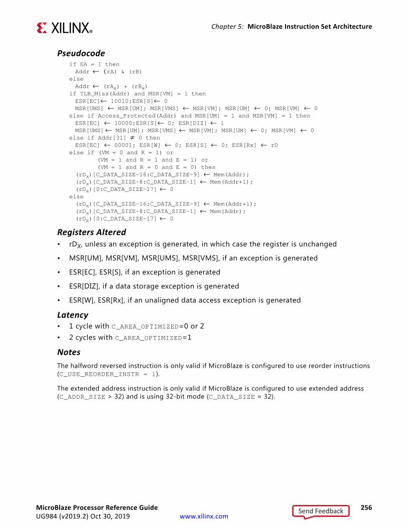
Chapter 5: MicroBlaze Instruction Set Architecture
Pseudocodeif EA = 1 thenAddr ← (rA) & (rB)
elseAddr ← (rAx) + (rBx)
if TLB_Miss(Addr) and MSR[VM] = 1 thenESR[EC]← 10010;ESR[S]← 0MSR[UMS] ← MSR[UM]; MSR[VMS] ← MSR[VM]; MSR[UM] ← 0; MSR[VM] ← 0
else if Access_Protected(Addr) and MSR[UM] = 1 and MSR[VM] = 1 thenESR[EC] ← 10000;ESR[S]← 0; ESR[DIZ] ← 1MSR[UMS]← MSR[UM]; MSR[VMS] ← MSR[VM]; MSR[UM] ← 0; MSR[VM] ← 0
else if Addr[31] ≠ 0 thenESR[EC] ← 00001; ESR[W] ← 0; ESR[S] ← 0; ESR[Rx] ← rD
else if (VM = 0 and R = 1) or (VM = 1 and R = 1 and E = 1) or (VM = 1 and R = 0 and E = 0) then
(rDx)[C_DATA_SIZE-16:C_DATA_SIZE-9] ← Mem(Addr);(rDx)[C_DATA_SIZE-8:C_DATA_SIZE-1] ← Mem(Addr+1);(rDx)[0:C_DATA_SIZE-17] ← 0
else (rDx)[C_DATA_SIZE-16:C_DATA_SIZE-9] ← Mem(Addr+1);(rDx)[C_DATA_SIZE-8:C_DATA_SIZE-1] ← Mem(Addr);(rDx)[0:C_DATA_SIZE-17] ← 0
Registers Altered• rDX, unless an exception is generated, in which case the register is unchanged
• MSR[UM], MSR[VM], MSR[UMS], MSR[VMS], if an exception is generated
• ESR[EC], ESR[S], if an exception is generated
• ESR[DIZ], if a data storage exception is generated
• ESR[W], ESR[Rx], if an unaligned data access exception is generated
Latency• 1 cycle with C_AREA_OPTIMIZED=0 or 2• 2 cycles with C_AREA_OPTIMIZED=1
NotesThe halfword reversed instruction is only valid if MicroBlaze is configured to use reorder instructions (C_USE_REORDER_INSTR = 1).
The extended address instruction is only valid if MicroBlaze is configured to use extended address (C_ADDR_SIZE > 32) and is using 32-bit mode (C_DATA_SIZE = 32).
MicroBlaze Processor Reference Guide 256UG984 (v2019.2) Oct 30, 2019 www.xilinx.com
Send Feedback
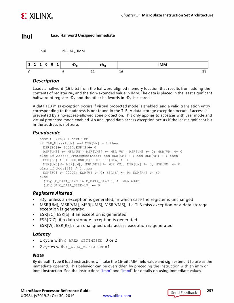
Chapter 5: MicroBlaze Instruction Set Architecture
lhui Load Halfword Unsigned Immediate
lhui rDx, rAx, IMM
1 1 1 0 0 1 rDX rAX IMM
0 6 11 16 31
DescriptionLoads a halfword (16 bits) from the halfword aligned memory location that results from adding the contents of register rAX and the sign-extended value in IMM. The data is placed in the least significant halfword of register rDX and the other halfwords in rDX is cleared.
A data TLB miss exception occurs if virtual protected mode is enabled, and a valid translation entry corresponding to the address is not found in the TLB. A data storage exception occurs if access is prevented by a no-access-allowed zone protection. This only applies to accesses with user mode and virtual protected mode enabled. An unaligned data access exception occurs if the least significant bit in the address is not zero.
PseudocodeAddr ← (rAX) + sext(IMM) if TLB_Miss(Addr) and MSR[VM] = 1 thenESR[EC]← 10010;ESR[S]← 0MSR[UMS] ← MSR[UM]; MSR[VMS] ← MSR[VM]; MSR[UM] ← 0; MSR[VM] ← 0
else if Access_Protected(Addr) and MSR[UM] = 1 and MSR[VM] = 1 thenESR[EC] ← 10000;ESR[S]← 0; ESR[DIZ] ← 1MSR[UMS]← MSR[UM]; MSR[VMS] ← MSR[VM]; MSR[UM] ← 0; MSR[VM] ← 0
else if Addr[31] ≠ 0 thenESR[EC] ← 00001; ESR[W] ← 0; ESR[S] ← 0; ESR[Rx] ← rD
else (rDX)[C_DATA_SIZE-16:C_DATA_SIZE-1] ← Mem(Addr) (rDX)[0:C_DATA_SIZE-17] ← 0
Registers Altered• rDX, unless an exception is generated, in which case the register is unchanged• MSR[UM], MSR[VM], MSR[UMS], MSR[VMS], if a TLB miss exception or a data storage
exception is generated• ESR[EC], ESR[S], if an exception is generated• ESR[DIZ], if a data storage exception is generated• ESR[W], ESR[Rx], if an unaligned data access exception is generated
Latency• 1 cycle with C_AREA_OPTIMIZED=0 or 2• 2 cycles with C_AREA_OPTIMIZED=1
NoteBy default, Type B load instructions will take the 16-bit IMM field value and sign extend it to use as the immediate operand. This behavior can be overridden by preceding the instruction with an imm or imml instruction. See the instructions “imm” and “imml” for details on using immediate values.
MicroBlaze Processor Reference Guide 257UG984 (v2019.2) Oct 30, 2019 www.xilinx.com
Send Feedback

Chapter 5: MicroBlaze Instruction Set Architecture
lw Load Word
lw rDx, rAx, rBx
lwr rDx, rAx, rBx
lwea rD, rA, rB
1 1 0 0 1 0 rDX rAX rBX 0 R 0 EA 0 0 0 0 0 0 0
0 6 11 16 21 31
DescriptionLoads a word (32 bits) from the word aligned memory location that results from adding the contents of registers rAX and rBX. The data is placed in least significant word of register rDX and the most significant word (if any) is cleared.
If the R bit is set, the bytes in the loaded word are reversed , loading data with the opposite endianness of the endianness defined by the E bit (if virtual protected mode is enabled).
If the EA bit is set, an extended address is used, formed by concatenating rA and rB instead of adding them.
A data TLB miss exception occurs if virtual protected mode is enabled, and a valid translation entry corresponding to the address is not found in the TLB.
A data storage exception occurs if access is prevented by a no-access-allowed zone protection. This only applies to accesses with user mode and virtual protected mode enabled.
An unaligned data access exception occurs if the two least significant bits in the address are not zero.
A privileged instruction error occurs if the EA bit is set, Physical Address Extension (PAE) is enabled, and the instruction is not explicitly allowed.
Pseudocodeif EA = 1 thenAddr ← (rA) & (rB)
elseAddr ← (rAX) + (rBX)
if TLB_Miss(Addr) and MSR[VM] = 1 thenESR[EC]← 10010;ESR[S]← 0MSR[UMS] ← MSR[UM]; MSR[VMS] ← MSR[VM]; MSR[UM] ← 0; MSR[VM] ← 0
else if Access_Protected(Addr) and MSR[UM] = 1 and MSR[VM] = 1 thenESR[EC] ← 10000;ESR[S]← 0; ESR[DIZ] ← 1MSR[UMS]← MSR[UM]; MSR[VMS] ← MSR[VM]; MSR[UM] ← 0; MSR[VM] ← 0
else if Addr[30:31] ≠ 0 thenESR[EC] ← 00001; ESR[W] ← 1; ESR[S] ← 0; ESR[Rx] ← rD
else (rDX[C_DATA_SIZE-32:C_DATA_SIZE-1]) ← Mem(Addr) (rDX[0:C_DATA_SIZE-33]) ← 0
MicroBlaze Processor Reference Guide 258UG984 (v2019.2) Oct 30, 2019 www.xilinx.com
Send Feedback
Chapter 5: MicroBlaze Instruction Set Architecture
Registers Altered• rDX, unless an exception is generated, in which case the register is unchanged• MSR[UM], MSR[VM], MSR[UMS], MSR[VMS], if a TLB miss exception or a data storage
exception is generated• ESR[EC], ESR[S], if an exception is generated• ESR[DIZ], if a data storage exception is generated• ESR[W], ESR[Rx], if an unaligned data access exception is generated
Latency• 1 cycle with C_AREA_OPTIMIZED=0 or 2• 2 cycles with C_AREA_OPTIMIZED=1
NotesThe word reversed instruction is only valid if MicroBlaze is configured to use reorder instructions (C_USE_REORDER_INSTR = 1).
The extended address instruction is only valid if MicroBlaze is configured to use extended address (C_ADDR_SIZE > 32) and is using 32-bit mode (C_DATA_SIZE = 32).
MicroBlaze Processor Reference Guide 259UG984 (v2019.2) Oct 30, 2019 www.xilinx.com
Send Feedback

Chapter 5: MicroBlaze Instruction Set Architecture
lwi Load Word Immediate
lwi rDX, rAX, IMM
1 1 1 0 1 0 rDX rAX IMM
0 6 11 16 31
DescriptionLoads a word (32 bits) from the word aligned memory location that results from adding the contents of register rAX and the sign-extended value IMM. The data is placed in the least significant word of register rDX and the most significant word (if any) is cleared.
A data TLB miss exception occurs if virtual protected mode is enabled, and a valid translation entry corresponding to the address is not found in the TLB.
A data storage exception occurs if access is prevented by a no-access-allowed zone protection. This only applies to accesses with user mode and virtual protected mode enabled.
An unaligned data access exception occurs if the two least significant bits in the address are not zero
PseudocodeAddr ← (rAX) + sext(IMM) if TLB_Miss(Addr) and MSR[VM] = 1 thenESR[EC]← 10010;ESR[S]← 0MSR[UMS] ← MSR[UM]; MSR[VMS] ← MSR[VM]; MSR[UM] ← 0; MSR[VM] ← 0
else if Access_Protected(Addr) and MSR[UM] = 1 and MSR[VM] = 1 thenESR[EC] ← 10000;ESR[S]← 0; ESR[DIZ] ← 1MSR[UMS]← MSR[UM]; MSR[VMS] ← MSR[VM]; MSR[UM] ← 0; MSR[VM] ← 0
else if Addr[30:31] ≠ 0 thenESR[EC] ← 00001; ESR[W] ← 1; ESR[S] ← 0; ESR[Rx] ← rD
else (rDX[C_DATA_SIZE-32:C_DATA_SIZE-1]) ← Mem(Addr); (rDX[0:C_DATA_SIZE-33]) ← 0
Registers Altered• rDX, unless an exception is generated, in which case the register is unchanged• MSR[UM], MSR[VM], MSR[UMS], MSR[VMS], if a TLB miss exception or a data storage
exception is generated• ESR[EC], ESR[S], if an exception is generated• ESR[DIZ], if a data storage exception is generated• ESR[W], ESR[Rx], if an unaligned data access exception is generated
Latency• 1 cycle with C_AREA_OPTIMIZED=0 or 2• 2 cycles with C_AREA_OPTIMIZED=1
NoteBy default, Type B load instructions will take the 16-bit IMM field value and sign extend it to use as the immediate operand. This behavior can be overridden by preceding the instruction with an imm or imml instruction. See the instructions “imm” and “imml” for details on using immediate values.
MicroBlaze Processor Reference Guide 260UG984 (v2019.2) Oct 30, 2019 www.xilinx.com
Send Feedback

Chapter 5: MicroBlaze Instruction Set Architecture
lwx Load Word Exclusive
lwx rD, rA, rB
1 1 0 0 1 0 rD rA rB 1 0 0 0 0 0 0 0 0 0 0
0 6 11 16 21 31
DescriptionLoads a word (32 bits) from the word aligned memory location that results from adding the contents of registers rA and rB. The data is placed in register rD, and the reservation bit is set. If an AXI4 interconnect with exclusive access enabled is used, and the interconnect response is not EXOKAY, the carry flag (MSR[C]) is set; otherwise the carry flag is cleared.
A data TLB miss exception occurs if virtual protected mode is enabled, and a valid translation entry corresponding to the address is not found in the TLB.
A data storage exception occurs if access is prevented by a no-access-allowed zone protection. This only applies to accesses with user mode and virtual protected mode enabled.
An unaligned data access exception will not occur, even if the two least significant bits in the address are not zero.
A data bus exception can occur when an AXI4 interconnect with exclusive access enabled is used, and the interconnect response is not EXOKAY, which means that an exclusive access cannot be handled.
Enabling AXI exclusive access ensures that the operation is protected from other bus masters, but requires that the addressed slave supports exclusive access. When exclusive access is not enabled, only the internal reservation bit is used. Exclusive access is enabled using the two parameters C_M_AXI_DP_EXCLUSIVE_ACCESS and C_M_AXI_DC_EXCLUSIVE_ACCESS for the peripheral and cache interconnect, respectively.
PseudocodeAddr ← (rA) + (rB) if TLB_Miss(Addr) and MSR[VM] = 1 then
ESR[EC]← 10010;ESR[S]← 0MSR[UMS] ← MSR[UM]; MSR[VMS] ← MSR[VM]; MSR[UM] ← 0; MSR[VM] ← 0
else if Access_Protected(Addr) and MSR[UM] = 1 and MSR[VM] = 1 thenESR[EC] ← 10000;ESR[S]← 0; ESR[DIZ] ← 1MSR[UMS]← MSR[UM]; MSR[VMS] ← MSR[VM]; MSR[UM] ← 0; MSR[VM] ← 0
else if AXI_Exclusive(Addr) and AXI_Response ≠ EXOKAY and MSR[EE] thenESR[EC] ← 00100;ESR[ECC]← 0;MSR[UMS]← MSR[UM]; MSR[VMS] ← MSR[VM]; MSR[UM] ← 0; MSR[VM] ← 0
else (rD) ← Mem(Addr); Reservation ← 1;if AXI_Exclusive(Addr) and AXI_Response ≠ EXOKAY thenMSR[C] ← 1
elseMSR[C] ← 0
MicroBlaze Processor Reference Guide 261UG984 (v2019.2) Oct 30, 2019 www.xilinx.com
Send Feedback
Chapter 5: MicroBlaze Instruction Set Architecture
Registers Altered• rD and MSR[C], unless an exception is generated, in which case they are unchanged• MSR[UM], MSR[VM], MSR[UMS], MSR[VMS], if a TLB miss exception or a data storage
exception is generated• ESR[EC], ESR[S], if an exception is generated• ESR[DIZ], if a data storage exception is generated
Latency• 1 cycle with C_AREA_OPTIMIZED=0 or 2• 2 cycles with C_AREA_OPTIMIZED=1
NotesThis instruction is used together with SWX to implement exclusive access, such as semaphores and spinlocks.
The carry flag (MSR[C]) might not be set immediately (dependent on pipeline stall behavior). The LWX instruction should not be immediately followed by an MSRCLR, MSRSET, MTS, or SRC instruction, to ensure the correct value of the carry flag is obtained.
MicroBlaze Processor Reference Guide 262UG984 (v2019.2) Oct 30, 2019 www.xilinx.com
Send Feedback
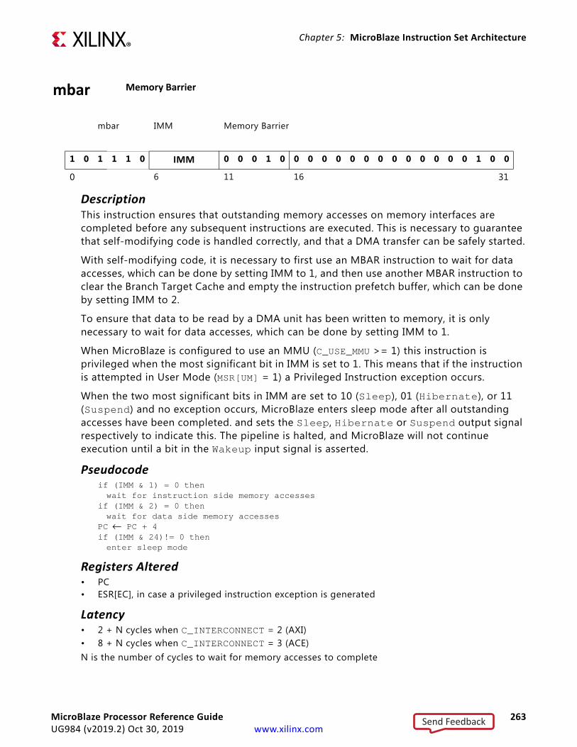
Chapter 5: MicroBlaze Instruction Set Architecture
mbar Memory Barrier
mbar IMM Memory Barrier
1 0 1 1 1 0 IMM 0 0 0 1 0 0 0 0 0 0 0 0 0 0 0 0 0 0 1 0 0
0 6 11 16 31
DescriptionThis instruction ensures that outstanding memory accesses on memory interfaces are completed before any subsequent instructions are executed. This is necessary to guarantee that self-modifying code is handled correctly, and that a DMA transfer can be safely started.
With self-modifying code, it is necessary to first use an MBAR instruction to wait for data accesses, which can be done by setting IMM to 1, and then use another MBAR instruction to clear the Branch Target Cache and empty the instruction prefetch buffer, which can be done by setting IMM to 2.
To ensure that data to be read by a DMA unit has been written to memory, it is only necessary to wait for data accesses, which can be done by setting IMM to 1.
When MicroBlaze is configured to use an MMU (C_USE_MMU >= 1) this instruction is privileged when the most significant bit in IMM is set to 1. This means that if the instruction is attempted in User Mode (MSR[UM] = 1) a Privileged Instruction exception occurs.
When the two most significant bits in IMM are set to 10 (Sleep), 01 (Hibernate), or 11 (Suspend) and no exception occurs, MicroBlaze enters sleep mode after all outstanding accesses have been completed. and sets the Sleep, Hibernate or Suspend output signal respectively to indicate this. The pipeline is halted, and MicroBlaze will not continue execution until a bit in the Wakeup input signal is asserted.
Pseudocodeif (IMM & 1) = 0 then wait for instruction side memory accesses
if (IMM & 2) = 0 then wait for data side memory accesses
PC ← PC + 4if (IMM & 24)!= 0 thenenter sleep mode
Registers Altered• PC• ESR[EC], in case a privileged instruction exception is generated
Latency• 2 + N cycles when C_INTERCONNECT = 2 (AXI)• 8 + N cycles when C_INTERCONNECT = 3 (ACE)N is the number of cycles to wait for memory accesses to complete
MicroBlaze Processor Reference Guide 263UG984 (v2019.2) Oct 30, 2019 www.xilinx.com
Send Feedback

Chapter 5: MicroBlaze Instruction Set Architecture
NotesThis instruction must not be preceded by an imm instruction, and must not be placed in a delay slot.
The assembler pseudo-instructions sleep, hibernate, and suspend can be used instead of “mbar 16”, “mbar 8”, and “mbar 24” respectively to enter sleep mode.
MicroBlaze Processor Reference Guide 264UG984 (v2019.2) Oct 30, 2019 www.xilinx.com
Send Feedback
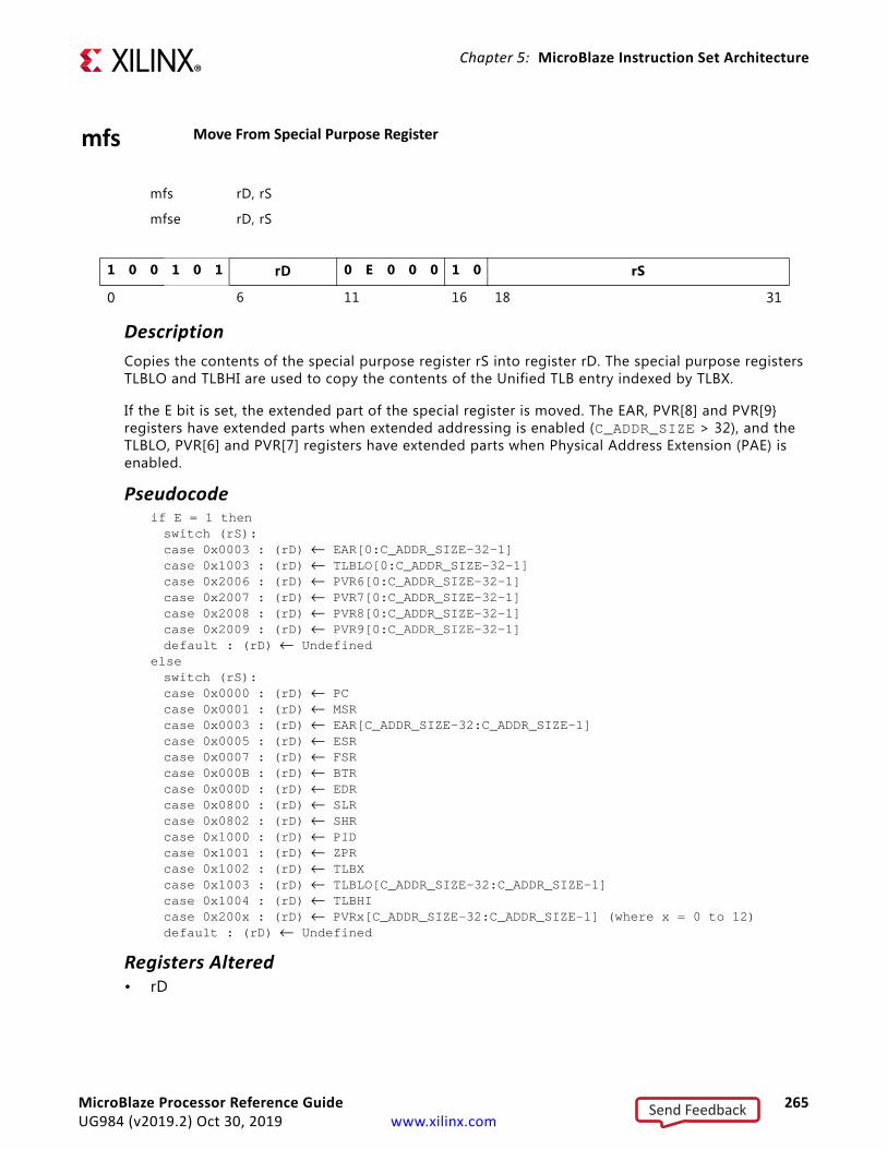
Chapter 5: MicroBlaze Instruction Set Architecture
mfs Move From Special Purpose Register
mfs rD, rS
mfse rD, rS
1 0 0 1 0 1 rD 0 E 0 0 0 1 0 rS
0 6 11 16 18 31
DescriptionCopies the contents of the special purpose register rS into register rD. The special purpose registers TLBLO and TLBHI are used to copy the contents of the Unified TLB entry indexed by TLBX.
If the E bit is set, the extended part of the special register is moved. The EAR, PVR[8] and PVR[9} registers have extended parts when extended addressing is enabled (C_ADDR_SIZE > 32), and the TLBLO, PVR[6] and PVR[7] registers have extended parts when Physical Address Extension (PAE) is enabled.
Pseudocodeif E = 1 thenswitch (rS):case 0x0003 : (rD) ← EAR[0:C_ADDR_SIZE-32-1]case 0x1003 : (rD) ← TLBLO[0:C_ADDR_SIZE-32-1]case 0x2006 : (rD) ← PVR6[0:C_ADDR_SIZE-32-1]case 0x2007 : (rD) ← PVR7[0:C_ADDR_SIZE-32-1]case 0x2008 : (rD) ← PVR8[0:C_ADDR_SIZE-32-1]case 0x2009 : (rD) ← PVR9[0:C_ADDR_SIZE-32-1]default : (rD) ← Undefined
elseswitch (rS):case 0x0000 : (rD) ← PCcase 0x0001 : (rD) ← MSRcase 0x0003 : (rD) ← EAR[C_ADDR_SIZE-32:C_ADDR_SIZE-1]case 0x0005 : (rD) ← ESRcase 0x0007 : (rD) ← FSRcase 0x000B : (rD) ← BTRcase 0x000D : (rD) ← EDRcase 0x0800 : (rD) ← SLRcase 0x0802 : (rD) ← SHRcase 0x1000 : (rD) ← PIDcase 0x1001 : (rD) ← ZPRcase 0x1002 : (rD) ← TLBXcase 0x1003 : (rD) ← TLBLO[C_ADDR_SIZE-32:C_ADDR_SIZE-1]case 0x1004 : (rD) ← TLBHIcase 0x200x : (rD) ← PVRx[C_ADDR_SIZE-32:C_ADDR_SIZE-1] (where x = 0 to 12)default : (rD) ← Undefined
Registers Altered• rD
MicroBlaze Processor Reference Guide 265UG984 (v2019.2) Oct 30, 2019 www.xilinx.com
Send Feedback
Chapter 5: MicroBlaze Instruction Set Architecture
Latency• 1 cycle
NotesTo refer to special purpose registers in assembly language, use rpc for PC, rmsr for MSR, rear for EAR, resr for ESR, rfsr for FSR, rbtr for BTR, redr for EDR, rslr for SLR, rshr for SHR, rpid for PID, rzpr for ZPR, rtlblo for TLBLO, rtlbhi for TLBHI, rtlbx for TLBX, and rpvr0 - rpvr12 for PVR0 - PVR12.
The value read from MSR might not include effects of the immediately preceding instruction (dependent on pipeline stall behavior). An instruction that does not affect MSR must precede the MFS instruction to guarantee correct MSR value.
The value read from FSR might not include effects of the immediately preceding instruction (dependent on pipeline stall behavior). An instruction that does not affect FSR must precede the MFS instruction to guarantee correct FSR value.
EAR, ESR and BTR are only valid as operands when at least one of the MicroBlaze C_*_EXCEPTION parameters are set to 1.
EDR is only valid as operand when the parameter C_FSL_EXCEPTION is set to 1 and the parameter C_FSL_LINKS is greater than 0.
FSR is only valid as an operand when the C_USE_FPU parameter is greater than 0.
SLR and SHR are only valid as an operand when the C_USE_STACK_PROTECTION parameter is set to 1.
PID, ZPR, TLBLO and TLBHI are only valid as operands when the parameter C_USE_MMU > 1 (User Mode) and the parameter C_MMU_TLB_ACCESS = 1 (Read) or 3 (Full).
TLBX is only valid as operand when the parameter C_USE_MMU > 1 (User Mode) and the parameter C_MMU_TLB_ACCESS > 0 (Minimal).
PVR0 is only valid as an operand when C_PVR is 1 (Basic) or 2 (Full), and PVR1 - PVR12 are only valid as operands when C_PVR is set to 2 (Full).
The extended instruction is only valid if MicroBlaze is configured to use extended address (C_ADDR_SIZE > 32).
MicroBlaze Processor Reference Guide 266UG984 (v2019.2) Oct 30, 2019 www.xilinx.com
Send Feedback
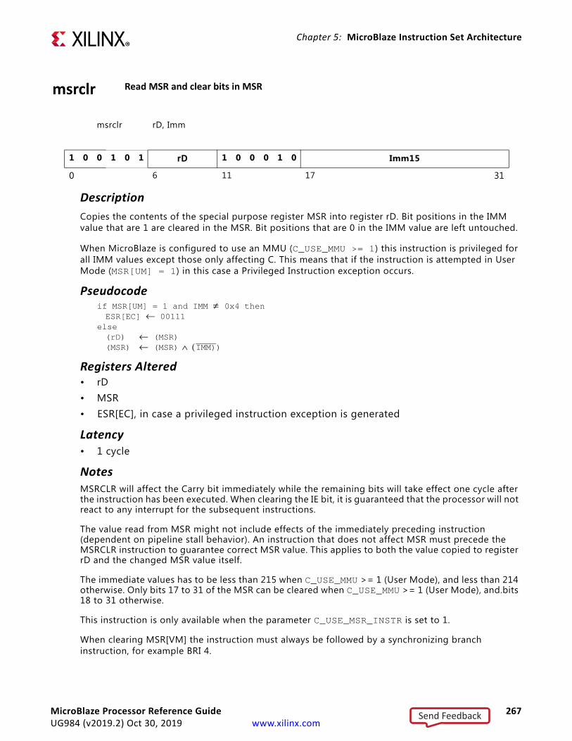
Chapter 5: MicroBlaze Instruction Set Architecture
msrclr Read MSR and clear bits in MSR
msrclr rD, Imm
1 0 0 1 0 1 rD 1 0 0 0 1 0 Imm15
0 6 11 17 31
DescriptionCopies the contents of the special purpose register MSR into register rD. Bit positions in the IMM value that are 1 are cleared in the MSR. Bit positions that are 0 in the IMM value are left untouched.
When MicroBlaze is configured to use an MMU (C_USE_MMU >= 1) this instruction is privileged for all IMM values except those only affecting C. This means that if the instruction is attempted in User Mode (MSR[UM] = 1) in this case a Privileged Instruction exception occurs.
Pseudocodeif MSR[UM] = 1 and IMM ≠ 0x4 thenESR[EC] ← 00111
else(rD) ← (MSR) (MSR) ← (MSR) ∧ (IMM))
Registers Altered• rD• MSR• ESR[EC], in case a privileged instruction exception is generated
Latency• 1 cycle
NotesMSRCLR will affect the Carry bit immediately while the remaining bits will take effect one cycle after the instruction has been executed. When clearing the IE bit, it is guaranteed that the processor will not react to any interrupt for the subsequent instructions.
The value read from MSR might not include effects of the immediately preceding instruction (dependent on pipeline stall behavior). An instruction that does not affect MSR must precede the MSRCLR instruction to guarantee correct MSR value. This applies to both the value copied to register rD and the changed MSR value itself.
The immediate values has to be less than 215 when C_USE_MMU >= 1 (User Mode), and less than 214 otherwise. Only bits 17 to 31 of the MSR can be cleared when C_USE_MMU >= 1 (User Mode), and.bits 18 to 31 otherwise.
This instruction is only available when the parameter C_USE_MSR_INSTR is set to 1.
When clearing MSR[VM] the instruction must always be followed by a synchronizing branch instruction, for example BRI 4.
MicroBlaze Processor Reference Guide 267UG984 (v2019.2) Oct 30, 2019 www.xilinx.com
Send Feedback
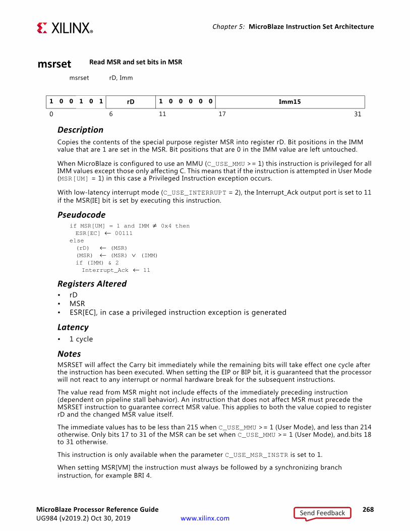
Chapter 5: MicroBlaze Instruction Set Architecture
msrset Read MSR and set bits in MSR
msrset rD, Imm
1 0 0 1 0 1 rD 1 0 0 0 0 0 Imm15
0 6 11 17 31
DescriptionCopies the contents of the special purpose register MSR into register rD. Bit positions in the IMM value that are 1 are set in the MSR. Bit positions that are 0 in the IMM value are left untouched.
When MicroBlaze is configured to use an MMU (C_USE_MMU >= 1) this instruction is privileged for all IMM values except those only affecting C. This means that if the instruction is attempted in User Mode (MSR[UM] = 1) in this case a Privileged Instruction exception occurs.
With low-latency interrupt mode (C_USE_INTERRUPT = 2), the Interrupt_Ack output port is set to 11 if the MSR{IE] bit is set by executing this instruction.
Pseudocodeif MSR[UM] = 1 and IMM ≠ 0x4 thenESR[EC] ← 00111
else(rD) ← (MSR) (MSR) ← (MSR) ∨ (IMM)if (IMM) & 2Interrupt_Ack ← 11
Registers Altered• rD• MSR• ESR[EC], in case a privileged instruction exception is generated
Latency• 1 cycle
NotesMSRSET will affect the Carry bit immediately while the remaining bits will take effect one cycle after the instruction has been executed. When setting the EIP or BIP bit, it is guaranteed that the processor will not react to any interrupt or normal hardware break for the subsequent instructions.
The value read from MSR might not include effects of the immediately preceding instruction (dependent on pipeline stall behavior). An instruction that does not affect MSR must precede the MSRSET instruction to guarantee correct MSR value. This applies to both the value copied to register rD and the changed MSR value itself.
The immediate values has to be less than 215 when C_USE_MMU >= 1 (User Mode), and less than 214 otherwise. Only bits 17 to 31 of the MSR can be set when C_USE_MMU >= 1 (User Mode), and.bits 18 to 31 otherwise.
This instruction is only available when the parameter C_USE_MSR_INSTR is set to 1.
When setting MSR[VM] the instruction must always be followed by a synchronizing branch instruction, for example BRI 4.
MicroBlaze Processor Reference Guide 268UG984 (v2019.2) Oct 30, 2019 www.xilinx.com
Send Feedback

Chapter 5: MicroBlaze Instruction Set Architecture
mts Move To Special Purpose Register
mts rS, rA
mtse rS, rA
1 0 0 1 0 1 0 E 0 0 0 rA 1 1 rS
0 6 11 16 18 31
DescriptionCopies the contents of register rD into the special purpose register rS. The special purpose registers TLBLO and TLBHI are used to copy to the Unified TLB entry indexed by TLBX.
If the E bit is set, the extended part of the special register is moved. The TLBLO register has an extended part when the Physical Address Extension (PAE) is enabled.
When MicroBlaze is configured to use an MMU (C_USE_MMU >= 1) this instruction is privileged. This means that if the instruction is attempted in User Mode (MSR[UM] = 1) a Privileged Instruction exception occurs.
With low-latency interrupt mode (C_USE_INTERRUPT = 2), the Interrupt_Ack output port is set to 11 if the MSR{IE] bit is set by executing this instruction.
Pseudocodeif MSR[UM] = 1 thenESR[EC] ← 00111
elseif E = 1 thenif (rS) = 0x1003 thenTLBLO[0:C_ADDR_SIZE-32-1] ← (rA)
elseswitch (rS)
case 0x0001 : MSR ← (rA) case 0x0007 : FSR ← (rA)
case 0x0800 : SLR ← (rA)case 0x0802 : SHR ← (rA)case 0x1000 : PID ← (rA)
case 0x1001 : ZPR ← (rA) case 0x1002 : TLBX ← (rA) case 0x1003 : TLBLO[C_ADDR_SIZE-32:C_ADDR_SIZE-1] ← (rA) case 0x1004 : TLBHI ← (rA) case 0x1005 : TLBSX ← (rA)
if (rS) = 0x0001 and (rA) & 2Interrupt_Ack ← 11
Registers Altered• rS
• ESR[EC], in case a privileged instruction exception is generated
MicroBlaze Processor Reference Guide 269UG984 (v2019.2) Oct 30, 2019 www.xilinx.com
Send Feedback
Chapter 5: MicroBlaze Instruction Set Architecture
Latency• 1 cycle
NotesWhen writing MSR using MTS, all bits take effect one cycle after the instruction has been executed. An MTS instruction writing MSR should never be followed back-to-back by an instruction that uses the MSR content. When clearing the IE bit, it is guaranteed that the processor will not react to any interrupt for the subsequent instructions. When setting the EIP or BIP bit, it is guaranteed that the processor will not react to any interrupt or normal hardware break for the subsequent instructions.
To refer to special purpose registers in assembly language, use rmsr for MSR, rfsr for FSR, rslr for SLR, rshr for SHR, rpid for PID, rzpr for ZPR, rtlblo for TLBLO, rtlbhi for TLBHI, rtlbx for TLBX, and rtlbsx for TLBSX.
The PC, ESR, EAR, BTR, EDR and PVR0 - PVR12 cannot be written by the MTS instruction.
The FSR is only valid as a destination if the MicroBlaze parameter C_USE_FPU is greater than 0.
The SLR and SHR are only valid as a destination if the MicroBlaze parameter C_USE_STACK_PROTECTION is set to 1.
PID, ZPR and TLBSX are only valid as destinations when the parameter C_USE_MMU > 1 (User Mode) and the parameter C_MMU_TLB_ACCESS > 1 (Read). TLBLO, TLBHI and TLBX are only valid as destinations when the parameter C_USE_MMU > 1 (User Mode).
When changing MSR[VM] or PID the instruction must always be followed by a synchronizing branch instruction, for example BRI 4.
After writing to TLBHI in order to invalidate one or more UTLB entries, an MBAR 1 instruction must be issued to ensure that coherency is preserved in a coherent multi-processor system.
When PAE is enabled, the entire TLBLO register must be written, by first using the extended instruction to write the most significant bits immediately followed by the least significant bits.
The extended instruction is only valid if MicroBlaze is configured to use the MMU in virtual mode (C_USE_MMU = 3) and extended address (C_ADDR_SIZE > 32).
MicroBlaze Processor Reference Guide 270UG984 (v2019.2) Oct 30, 2019 www.xilinx.com
Send Feedback

Chapter 5: MicroBlaze Instruction Set Architecture
mul Multiply
mul rD, rA, rB
0 1 0 0 0 0 rD rA rB 0 0 0 0 0 0 0 0 0 0 0
0 6 11 16 21 31
DescriptionMultiplies the contents of registers rA and rB and puts the result in register rD. This is a 32-bit by 32-bit multiplication that will produce a 64-bit result. The least significant word of this value is placed in rD. The most significant word is discarded.
Pseudocode(rD) ← LSW( (rA) × (rB) )
Registers Altered• rD
Latency• 1 cycle with C_AREA_OPTIMIZED=0 or 2• 3 cycles with C_AREA_OPTIMIZED=1
NoteThis instruction is only valid if the target architecture has multiplier primitives, and if present, the MicroBlaze parameter C_USE_HW_MUL is greater than 0.
MicroBlaze Processor Reference Guide 271UG984 (v2019.2) Oct 30, 2019 www.xilinx.com
Send Feedback
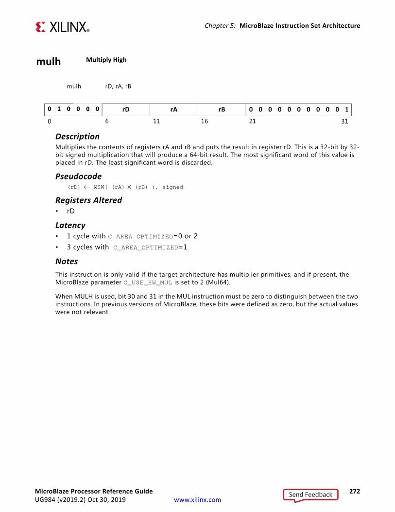
Chapter 5: MicroBlaze Instruction Set Architecture
mulh Multiply High
mulh rD, rA, rB
0 1 0 0 0 0 rD rA rB 0 0 0 0 0 0 0 0 0 0 1
0 6 11 16 21 31
DescriptionMultiplies the contents of registers rA and rB and puts the result in register rD. This is a 32-bit by 32-bit signed multiplication that will produce a 64-bit result. The most significant word of this value is placed in rD. The least significant word is discarded.
Pseudocode(rD) ← MSW( (rA) × (rB) ), signed
Registers Altered• rD
Latency• 1 cycle with C_AREA_OPTIMIZED=0 or 2• 3 cycles with C_AREA_OPTIMIZED=1
NotesThis instruction is only valid if the target architecture has multiplier primitives, and if present, the MicroBlaze parameter C_USE_HW_MUL is set to 2 (Mul64).
When MULH is used, bit 30 and 31 in the MUL instruction must be zero to distinguish between the two instructions. In previous versions of MicroBlaze, these bits were defined as zero, but the actual values were not relevant.
MicroBlaze Processor Reference Guide 272UG984 (v2019.2) Oct 30, 2019 www.xilinx.com
Send Feedback

Chapter 5: MicroBlaze Instruction Set Architecture
mulhu Multiply High Unsigned
mulhu rD, rA, rB
0 1 0 0 0 0 rD rA rB 0 0 0 0 0 0 0 0 0 1 1
0 6 11 16 21 31
DescriptionMultiplies the contents of registers rA and rB and puts the result in register rD. This is a 32-bit by 32-bit unsigned multiplication that will produce a 64-bit unsigned result. The most significant word of this value is placed in rD. The least significant word is discarded.
Pseudocode(rD) ← MSW( (rA) × (rB) ), unsigned
Registers Altered• rD
Latency• 1 cycle with C_AREA_OPTIMIZED=0 or 2• 3 cycles with C_AREA_OPTIMIZED=1
NotesThis instruction is only valid if the target architecture has multiplier primitives, and if present, the MicroBlaze parameter C_USE_HW_MUL is set to 2 (Mul64).
When MULHU is used, bit 30 and 31 in the MUL instruction must be zero to distinguish between the two instructions. In previous versions of MicroBlaze, these bits were defined as zero, but the actual values were not relevant.
MicroBlaze Processor Reference Guide 273UG984 (v2019.2) Oct 30, 2019 www.xilinx.com
Send Feedback

Chapter 5: MicroBlaze Instruction Set Architecture
mulhsu Multiply High Signed Unsigned
mulhsu rD, rA, rB
0 1 0 0 0 0 rD rA rB 0 0 0 0 0 0 0 0 0 1 0
0 6 11 16 21 31
DescriptionMultiplies the contents of registers rA and rB and puts the result in register rD. This is a 32-bit signed by 32-bit unsigned multiplication that will produce a 64-bit signed result. The most significant word of this value is placed in rD. The least significant word is discarded.
Pseudocode(rD) ← MSW( (rA), signed × (rB), unsigned ), signed
Registers Altered• rD
Latency• 1 cycle with C_AREA_OPTIMIZED=0 or 2• 3 cycles with C_AREA_OPTIMIZED=1
NotesThis instruction is only valid if the target architecture has multiplier primitives, and if present, the MicroBlaze parameter C_USE_HW_MUL is set to 2 (Mul64).
When MULHSU is used, bit 30 and 31 in the MUL instruction must be zero to distinguish between the two instructions. In previous versions of MicroBlaze, these bits were defined as zero, but the actual values were not relevant.
MicroBlaze Processor Reference Guide 274UG984 (v2019.2) Oct 30, 2019 www.xilinx.com
Send Feedback

Chapter 5: MicroBlaze Instruction Set Architecture
muli Multiply Immediate
muli rD, rA, IMM
0 1 1 0 0 0 rD rA IMM
0 6 11 16 31
DescriptionMultiplies the contents of registers rA and the value IMM, sign-extended to 32 bits; and puts the result in register rD. This is a 32-bit by 32-bit multiplication that will produce a 64-bit result. The least significant word of this value is placed in rD. The most significant word is discarded.
Pseudocode(rD) ← LSW( (rA) × sext(IMM) )
Registers Altered• rD
Latency• 1 cycle with C_AREA_OPTIMIZED=0 or 2• 3 cycles with C_AREA_OPTIMIZED=1
NotesBy default, Type B Instructions will take the 16-bit IMM field value and sign extend it to 32 bits to use as the immediate operand. This behavior can be overridden by preceding the Type B instruction with an imm instruction. See the instruction “imm” for details on using 32-bit immediate values.
This instruction is only valid if the target architecture has multiplier primitives, and if present, the MicroBlaze parameter C_USE_HW_MUL is greater than 0.
MicroBlaze Processor Reference Guide 275UG984 (v2019.2) Oct 30, 2019 www.xilinx.com
Send Feedback
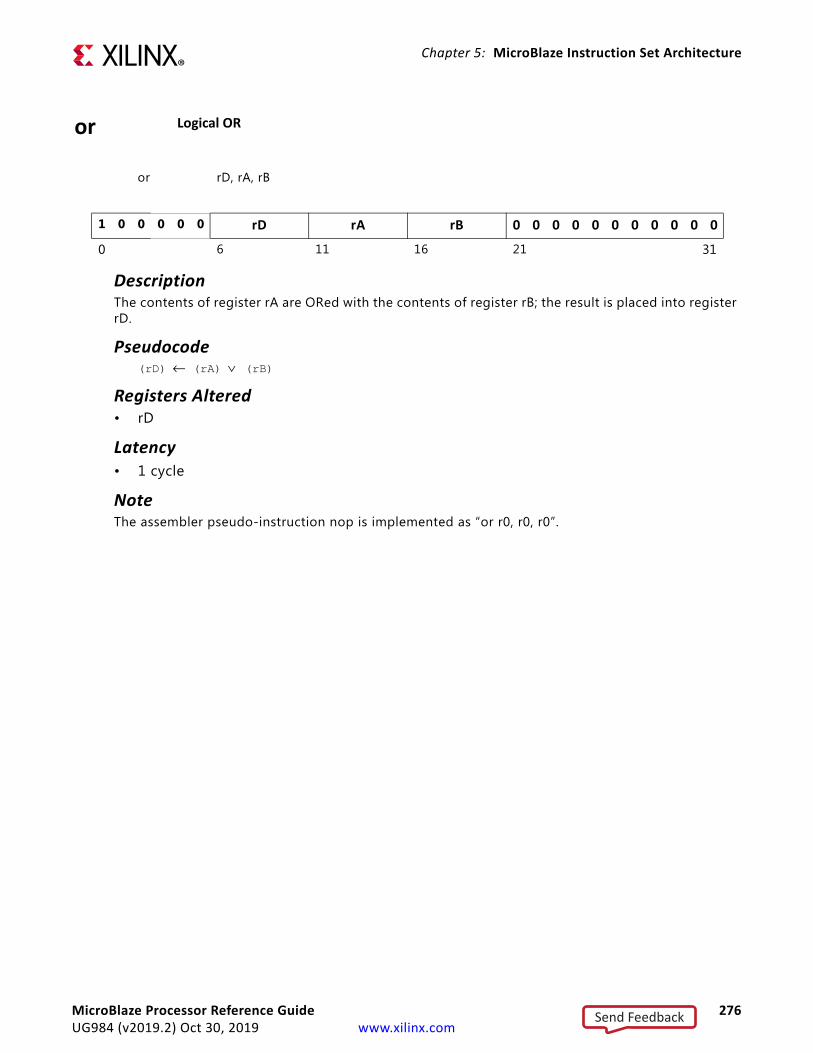
Chapter 5: MicroBlaze Instruction Set Architecture
or Logical OR
or rD, rA, rB
1 0 0 0 0 0 rD rA rB 0 0 0 0 0 0 0 0 0 0 0
0 6 11 16 21 31
DescriptionThe contents of register rA are ORed with the contents of register rB; the result is placed into register rD.
Pseudocode(rD) ← (rA) ∨ (rB)
Registers Altered• rD
Latency• 1 cycle
NoteThe assembler pseudo-instruction nop is implemented as “or r0, r0, r0”.
MicroBlaze Processor Reference Guide 276UG984 (v2019.2) Oct 30, 2019 www.xilinx.com
Send Feedback

Chapter 5: MicroBlaze Instruction Set Architecture
ori Logical OR with Immediate
ori rD, rA, IMM
1 0 1 0 0 0 rD rA IMM
0 6 11 16 31
DescriptionThe contents of register rA are ORed with the extended IMM field, sign-extended to 32 bits; the result is placed into register rD.
Pseudocode(rD) ← (rA) ∨ sext(IMM)
Registers Altered• rD
Latency• 1 cycle
NoteBy default, Type B Instructions will take the 16-bit IMM field value and sign extend it to 32 bits to use as the immediate operand. This behavior can be overridden by preceding the Type B instruction with an imm instruction. See the instruction “imm” for details on using 32-bit immediate values.
MicroBlaze Processor Reference Guide 277UG984 (v2019.2) Oct 30, 2019 www.xilinx.com
Send Feedback
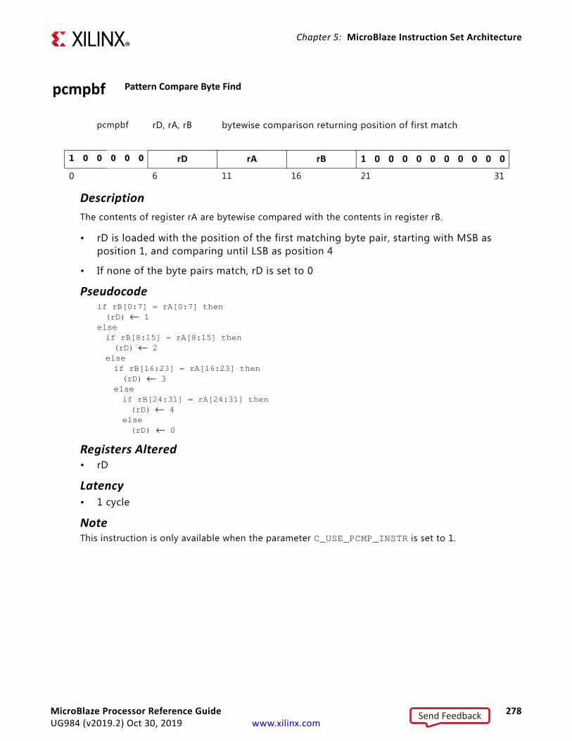
Chapter 5: MicroBlaze Instruction Set Architecture
pcmpbf Pattern Compare Byte Find
pcmpbf rD, rA, rB bytewise comparison returning position of first match
1 0 0 0 0 0 rD rA rB 1 0 0 0 0 0 0 0 0 0 0
0 6 11 16 21 31
DescriptionThe contents of register rA are bytewise compared with the contents in register rB.
• rD is loaded with the position of the first matching byte pair, starting with MSB as position 1, and comparing until LSB as position 4
• If none of the byte pairs match, rD is set to 0
Pseudocodeif rB[0:7] = rA[0:7] then(rD) ← 1
elseif rB[8:15] = rA[8:15] then(rD) ← 2
elseif rB[16:23] = rA[16:23] then(rD) ← 3
elseif rB[24:31] = rA[24:31] then(rD) ← 4
else(rD) ← 0
Registers Altered• rD
Latency• 1 cycle
NoteThis instruction is only available when the parameter C_USE_PCMP_INSTR is set to 1.
MicroBlaze Processor Reference Guide 278UG984 (v2019.2) Oct 30, 2019 www.xilinx.com
Send Feedback

Chapter 5: MicroBlaze Instruction Set Architecture
pcmpeq Pattern Compare Equal
pcmpeq rD, rA, rB equality comparison with a positive boolean result
1 0 0 0 1 0 rD rA rB 1 0 0 0 0 0 0 0 0 0 0
0 6 11 16 21 31
DescriptionThe contents of register rA are compared with the contents in register rB.
• rD is loaded with 1 if they match, and 0 if not
Pseudocodeif (rB) = (rA) then(rD) ← 1
else(rD) ← 0
Registers Altered• rD
Latency• 1 cycle
NoteThis instruction is only available when the parameter C_USE_PCMP_INSTR is set to 1.
MicroBlaze Processor Reference Guide 279UG984 (v2019.2) Oct 30, 2019 www.xilinx.com
Send Feedback

Chapter 5: MicroBlaze Instruction Set Architecture
pcmpne Pattern Compare Not Equal
pcmpne rD, rA, rB equality comparison with a negative boolean result
1 0 0 0 1 1 rD rA rB 1 0 0 0 0 0 0 0 0 0 0
0 6 11 16 21 31
DescriptionThe contents of register rA are compared with the contents in register rB.
• rD is loaded with 0 if they match, and 1 if not
Pseudocodeif (rB) = (rA) then(rD) ← 0
else(rD) ← 1
Registers Altered• rD
Latency• 1 cycle
NoteThis instruction is only available when the parameter C_USE_PCMP_INSTR is set to 1.
MicroBlaze Processor Reference Guide 280UG984 (v2019.2) Oct 30, 2019 www.xilinx.com
Send Feedback

Chapter 5: MicroBlaze Instruction Set Architecture
put Put to stream interface
naput rA, FSLx put data to link xn = non-blockinga = atomic
tnaput FSLx put data to link x test-onlyn = non-blockinga = atomic
ncaput rA, FSLx put control to link xn = non-blockinga = atomic
tncaput FSLx put control to link x test-onlyn = non-blockinga = atomic
0 1 1 0 1 1 0 0 0 0 0 rA 1 n c t a 0 0 0 0 0 0 0 FSLx
0 6 11 16 28 31
DescriptionMicroBlaze will write the value from register rA to the link x interface. If the available number of links set by C_FSL_LINKS is less than or equal to FSLx, link 0 is used.
The put instruction has 16 variants.
The blocking versions (when ‘n’ is ‘0’) will stall MicroBlaze until there is space available in the interface. The non-blocking versions will not stall MicroBlaze and will set carry to ‘0’ if space was available and to ‘1’ if no space was available.
All data put instructions (when ‘c’ is ‘0’) will set the control bit to the interface to ‘0’ and all control put instructions (when ‘c’ is ‘1’) will set the control bit to ‘1’.
The test versions (when ‘t’ bit is ‘1’) will be handled as the normal case, except that the write signal to the link is not asserted (thus no source register is required).
Atomic versions (when ‘a’ bit is ‘1’) are not interruptible. This means that a sequence of atomic instructions can be grouped together without an interrupt breaking the program flow. However, note that exceptions might still occur.
When MicroBlaze is configured to use an MMU (C_USE_MMU >= 1) and not explicitly allowed by setting C_MMU_PRIVILEGED_INSTR to 1 these instructions are privileged. This means that if these instructions are attempted in User Mode (MSR[UM] = 1) a Privileged Instruction exception occurs.
MicroBlaze Processor Reference Guide 281UG984 (v2019.2) Oct 30, 2019 www.xilinx.com
Send Feedback

Chapter 5: MicroBlaze Instruction Set Architecture
Pseudocodeif MSR[UM] = 1 thenESR[EC] ← 00111
elsex ← FSLxif x >= C_FSL_LINKS thenx ← 0
Mx_AXIS_TDATA ← (rA)if (n = 1) thenMSR[Carry] ← Mx_AXIS_TVALID ∧ Mx_AXIS_TREADY
Mx_AXIS_TLAST ← C
Registers Altered• MSR[Carry]• ESR[EC], in case a privileged instruction exception is generated
Latency• 1 cycle with C_AREA_OPTIMIZED=0 or 2• 2 cycles with C_AREA_OPTIMIZED=1
The blocking versions of this instruction will stall the pipeline of MicroBlaze until the instruction can be completed. Interrupts are served when the parameter C_USE_EXTENDED_FSL_INSTR is set to 1, and the instruction is not atomic.
NotesTo refer to an FSLx interface in assembly language, use rfsl0, rfsl1, ... rfsl15.
The blocking versions of this instruction should not be placed in a delay slot when the parameter C_USE_EXTENDED_FSL_INSTR is set to 1, since this prevents interrupts from being served.
These instructions are only available when the MicroBlaze parameter C_FSL_LINKS is greater than 0.
The extended instructions (test and atomic versions) are only available when the MicroBlaze parameter C_USE_EXTENDED_FSL_INSTR is set to 1.
It is not recommended to allow these instructions in user mode, unless absolutely necessary for performance reasons, since that removes all hardware protection preventing incorrect use of a link.
MicroBlaze Processor Reference Guide 282UG984 (v2019.2) Oct 30, 2019 www.xilinx.com
Send Feedback
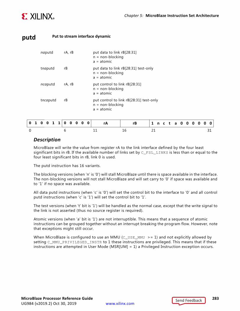
Chapter 5: MicroBlaze Instruction Set Architecture
putd Put to stream interface dynamic
naputd rA, rB put data to link rB[28:31] n = non-blocking a = atomic
tnaputd rB put data to link rB[28:31] test-only n = non-blocking a = atomic
ncaputd rA, rB put control to link rB[28:31] n = non-blocking a = atomic
tncaputd rB put control to link rB[28:31] test-only n = non-blocking a = atomic
0 1 0 0 1 1 0 0 0 0 0 rA rB 1 n c t a 0 0 0 0 0 0
0 6 11 16 21 31
DescriptionMicroBlaze will write the value from register rA to the link interface defined by the four least significant bits in rB. If the available number of links set by C_FSL_LINKS is less than or equal to the four least significant bits in rB, link 0 is used.
The putd instruction has 16 variants.
The blocking versions (when ‘n’ is ‘0’) will stall MicroBlaze until there is space available in the interface. The non-blocking versions will not stall MicroBlaze and will set carry to ‘0’ if space was available and to ‘1’ if no space was available.
All data putd instructions (when ‘c’ is ‘0’) will set the control bit to the interface to ‘0’ and all control putd instructions (when ‘c’ is ‘1’) will set the control bit to ‘1’.
The test versions (when ‘t’ bit is ‘1’) will be handled as the normal case, except that the write signal to the link is not asserted (thus no source register is required).
Atomic versions (when ‘a’ bit is ‘1’) are not interruptible. This means that a sequence of atomic instructions can be grouped together without an interrupt breaking the program flow. However, note that exceptions might still occur.
When MicroBlaze is configured to use an MMU (C_USE_MMU >= 1) and not explicitly allowed by setting C_MMU_PRIVILEGED_INSTR to 1 these instructions are privileged. This means that if these instructions are attempted in User Mode (MSR[UM] = 1) a Privileged Instruction exception occurs.
MicroBlaze Processor Reference Guide 283UG984 (v2019.2) Oct 30, 2019 www.xilinx.com
Send Feedback
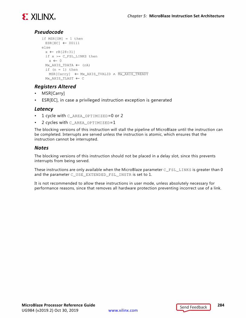
Chapter 5: MicroBlaze Instruction Set Architecture
Pseudocodeif MSR[UM] = 1 thenESR[EC] ← 00111
elsex ← rB[28:31]if x >= C_FSL_LINKS thenx ← 0
Mx_AXIS_TDATA ← (rA)if (n = 1) thenMSR[Carry] ← Mx_AXIS_TVALID ∧ Mx_AXIS_TREADY
Mx_AXIS_TLAST ← C
Registers Altered• MSR[Carry]• ESR[EC], in case a privileged instruction exception is generated
Latency• 1 cycle with C_AREA_OPTIMIZED=0 or 2• 2 cycles with C_AREA_OPTIMIZED=1The blocking versions of this instruction will stall the pipeline of MicroBlaze until the instruction can be completed. Interrupts are served unless the instruction is atomic, which ensures that the instruction cannot be interrupted.
NotesThe blocking versions of this instruction should not be placed in a delay slot, since this prevents interrupts from being served.
These instructions are only available when the MicroBlaze parameter C_FSL_LINKS is greater than 0 and the parameter C_USE_EXTENDED_FSL_INSTR is set to 1.
It is not recommended to allow these instructions in user mode, unless absolutely necessary for performance reasons, since that removes all hardware protection preventing incorrect use of a link.
MicroBlaze Processor Reference Guide 284UG984 (v2019.2) Oct 30, 2019 www.xilinx.com
Send Feedback
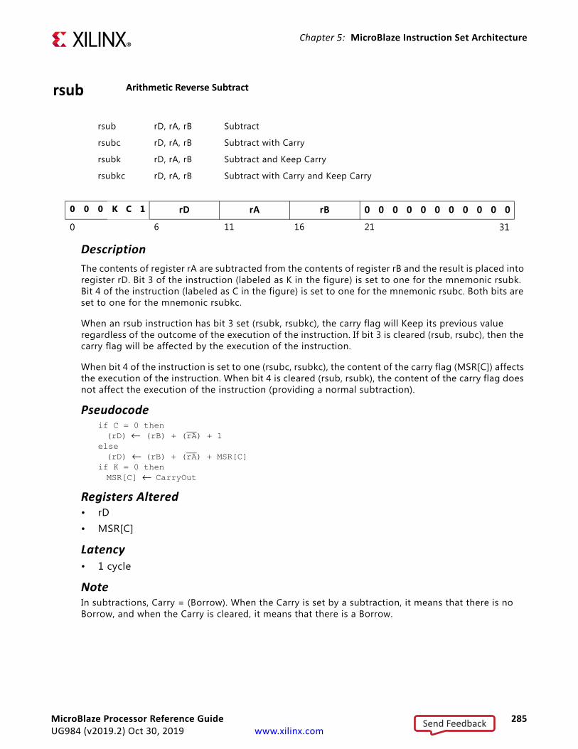
Chapter 5: MicroBlaze Instruction Set Architecture
rsub Arithmetic Reverse Subtract
rsub rD, rA, rB Subtract
rsubc rD, rA, rB Subtract with Carry
rsubk rD, rA, rB Subtract and Keep Carry
rsubkc rD, rA, rB Subtract with Carry and Keep Carry
0 0 0 K C 1 rD rA rB 0 0 0 0 0 0 0 0 0 0 0
0 6 11 16 21 31
DescriptionThe contents of register rA are subtracted from the contents of register rB and the result is placed into register rD. Bit 3 of the instruction (labeled as K in the figure) is set to one for the mnemonic rsubk. Bit 4 of the instruction (labeled as C in the figure) is set to one for the mnemonic rsubc. Both bits are set to one for the mnemonic rsubkc.
When an rsub instruction has bit 3 set (rsubk, rsubkc), the carry flag will Keep its previous value regardless of the outcome of the execution of the instruction. If bit 3 is cleared (rsub, rsubc), then the carry flag will be affected by the execution of the instruction.
When bit 4 of the instruction is set to one (rsubc, rsubkc), the content of the carry flag (MSR[C]) affects the execution of the instruction. When bit 4 is cleared (rsub, rsubk), the content of the carry flag does not affect the execution of the instruction (providing a normal subtraction).
Pseudocodeif C = 0 then(rD) ← (rB) + (rA) + 1
else(rD) ← (rB) + (rA) + MSR[C]
if K = 0 thenMSR[C] ← CarryOut
Registers Altered• rD• MSR[C]
Latency• 1 cycle
NoteIn subtractions, Carry = (Borrow). When the Carry is set by a subtraction, it means that there is no Borrow, and when the Carry is cleared, it means that there is a Borrow.
MicroBlaze Processor Reference Guide 285UG984 (v2019.2) Oct 30, 2019 www.xilinx.com
Send Feedback

Chapter 5: MicroBlaze Instruction Set Architecture
rsubi Arithmetic Reverse Subtract Immediate
rsubi rD, rA, IMM Subtract Immediate
rsubic rD, rA, IMM Subtract Immediate with Carry
rsubik rD, rA, IMM Subtract Immediate and Keep Carry
rsubikc rD, rA, IMM Subtract Immediate with Carry and Keep Carry
0 0 1 K C 1 rD rA IMM
0 6 11 16 31
DescriptionThe contents of register rA are subtracted from the value of IMM, sign-extended to 32 bits, and the result is placed into register rD. Bit 3 of the instruction (labeled as K in the figure) is set to one for the mnemonic rsubik. Bit 4 of the instruction (labeled as C in the figure) is set to one for the mnemonic rsubic. Both bits are set to one for the mnemonic rsubikc.
When an rsubi instruction has bit 3 set (rsubik, rsubikc), the carry flag will Keep its previous value regardless of the outcome of the execution of the instruction. If bit 3 is cleared (rsubi, rsubic), then the carry flag will be affected by the execution of the instruction. When bit 4 of the instruction is set to one (rsubic, rsubikc), the content of the carry flag (MSR[C]) affects the execution of the instruction. When bit 4 is cleared (rsubi, rsubik), the content of the carry flag does not affect the execution of the instruction (providing a normal subtraction).
Pseudocodeif C = 0 then(rD) ← sext(IMM) + (rA) + 1
else(rD) ← sext(IMM) + (rA) + MSR[C]
if K = 0 thenMSR[C] ← CarryOut
Registers Altered• rD• MSR[C]
Latency• 1 cycle
NoteIn subtractions, Carry = (Borrow). When the Carry is set by a subtraction, it means that there is no Borrow, and when the Carry is cleared, it means that there is a Borrow. By default, Type B Instructions will take the 16-bit IMM field value and sign extend it to 32 bits to use as the immediate operand. This behavior can be overridden by preceding the Type B instruction with an imm instruction. See the instruction “imm” for details on using 32-bit immediate values.
MicroBlaze Processor Reference Guide 286UG984 (v2019.2) Oct 30, 2019 www.xilinx.com
Send Feedback

Chapter 5: MicroBlaze Instruction Set Architecture
rtbd Return from Break
rtbd rAX, IMM
1 0 1 1 0 1 1 0 0 1 0 rAX IMM
0 6 11 16 31
DescriptionReturn from break will branch to the location specified by the contents of rAX plus the sign-extended IMM field. It will also enable breaks after execution by clearing the BIP flag in the MSR.
This instruction always has a delay slot. The instruction following the RTBD is always executed before the branch target. That delay slot instruction has breaks disabled.
When MicroBlaze is configured to use an MMU (C_USE_MMU >= 1) this instruction is privileged. This means that if the instruction is attempted in User Mode (MSR[UM] = 1) a Privileged Instruction exception occurs.
Pseudocodeif MSR[UM] = 1 thenESR[EC] ← 00111
elsePC ← (rAX) + sext(IMM)allow following instruction to complete executionMSR[BIP] ← 0MSR[UM] ← MSR[UMS]MSR[VM] ← MSR[VMS]
Registers Altered• PC• MSR[BIP], MSR[UM], MSR[VM]• ESR[EC], in case a privileged instruction exception is generated
Latency• 2 cycles
NotesConvention is to use general purpose register r16 as rAX.
A delay slot must not be used by the following: imm, branch, or break instructions. Interrupts and external hardware breaks are deferred until after the delay slot branch has been completed.
MicroBlaze Processor Reference Guide 287UG984 (v2019.2) Oct 30, 2019 www.xilinx.com
Send Feedback

Chapter 5: MicroBlaze Instruction Set Architecture
rtid Return from Interrupt
rtid rAX, IMM
1 0 1 1 0 1 1 0 0 0 1 rAX IMM
0 6 11 16 31
DescriptionReturn from interrupt will branch to the location specified by the contents of rAX plus the sign-extended IMM field. It will also enable interrupts after execution.
This instruction always has a delay slot. The instruction following the RTID is always executed before the branch target. That delay slot instruction has interrupts disabled.
When MicroBlaze is configured to use an MMU (C_USE_MMU >= 1) this instruction is privileged. This means that if the instruction is attempted in User Mode (MSR[UM] = 1) a Privileged Instruction exception occurs.
With low-latency interrupt mode (C_USE_INTERRUPT = 2), the Interrupt_Ack output port is set to 10 when this instruction is executed, and subsequently to 11 when the MSR{IE] bit is set.
Pseudocodeif MSR[UM] = 1 thenESR[EC] ← 00111
elsePC ← (rAX) + sext(IMM)Interrupt_Ack ← 10allow following instruction to complete executionMSR[IE] ← 1MSR[UM] ← MSR[UMS]MSR[VM] ← MSR[VMS]Interrupt_Ack ← 11
Registers Altered• PC• MSR[IE], MSR[UM], MSR[VM]• ESR[EC], in case a privileged instruction exception is generated
Latency• 2 cycles
NotesConvention is to use general purpose register r14 as rAX.
A delay slot must not be used by the following: imm, branch, or break instructions. Interrupts and external hardware breaks are deferred until after the delay slot branch has been completed.
MicroBlaze Processor Reference Guide 288UG984 (v2019.2) Oct 30, 2019 www.xilinx.com
Send Feedback
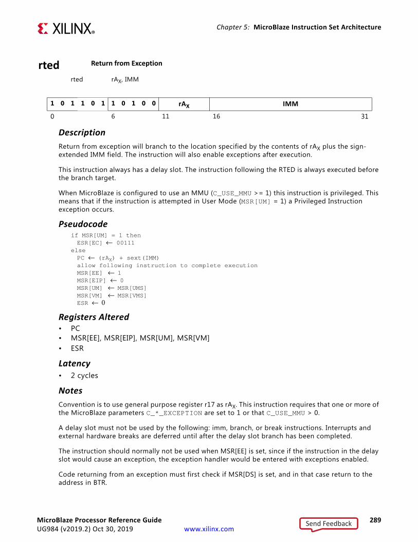
Chapter 5: MicroBlaze Instruction Set Architecture
rted Return from Exception
rted rAX, IMM
1 0 1 1 0 1 1 0 1 0 0 rAX IMM
0 6 11 16 31
DescriptionReturn from exception will branch to the location specified by the contents of rAX plus the sign-extended IMM field. The instruction will also enable exceptions after execution.
This instruction always has a delay slot. The instruction following the RTED is always executed before the branch target.
When MicroBlaze is configured to use an MMU (C_USE_MMU >= 1) this instruction is privileged. This means that if the instruction is attempted in User Mode (MSR[UM] = 1) a Privileged Instruction exception occurs.
Pseudocodeif MSR[UM] = 1 thenESR[EC] ← 00111
elsePC ← (rAX) + sext(IMM)allow following instruction to complete executionMSR[EE] ← 1MSR[EIP] ← 0MSR[UM] ← MSR[UMS]MSR[VM] ← MSR[VMS]ESR ← 0
Registers Altered• PC• MSR[EE], MSR[EIP], MSR[UM], MSR[VM]• ESR
Latency• 2 cycles
NotesConvention is to use general purpose register r17 as rAX. This instruction requires that one or more of the MicroBlaze parameters C_*_EXCEPTION are set to 1 or that C_USE_MMU > 0.
A delay slot must not be used by the following: imm, branch, or break instructions. Interrupts and external hardware breaks are deferred until after the delay slot branch has been completed.
The instruction should normally not be used when MSR[EE] is set, since if the instruction in the delay slot would cause an exception, the exception handler would be entered with exceptions enabled.
Code returning from an exception must first check if MSR[DS] is set, and in that case return to the address in BTR.
MicroBlaze Processor Reference Guide 289UG984 (v2019.2) Oct 30, 2019 www.xilinx.com
Send Feedback

Chapter 5: MicroBlaze Instruction Set Architecture
rtsd Return from Subroutine
rtsd rAX, IMM
1 0 1 1 0 1 1 0 0 0 0 rAX IMM
0 6 11 16 31
DescriptionReturn from subroutine will branch to the location specified by the contents of rAX plus the sign-extended IMM field.
This instruction always has a delay slot. The instruction following the RTSD is always executed before the branch target.
PseudocodePC ← (rAX) + sext(IMM)allow following instruction to complete execution
Registers Altered• PC
Latency• 1 cycle (if successful branch prediction occurs)• 2 cycles (with Branch Target Cache disabled)• 3 cycles (if branch prediction mispredict occurs with C_AREA_OPTIMIZED=0)• 7-9 cycles (if a branch prediction mispredict occurs with C_AREA_OPTIMIZED=2)
NotesConvention is to use general purpose register r15 as rAX.
A delay slot must not be used by the following: imm, branch, or break instructions. Interrupts and external hardware breaks are deferred until after the delay slot branch has been completed.
MicroBlaze Processor Reference Guide 290UG984 (v2019.2) Oct 30, 2019 www.xilinx.com
Send Feedback
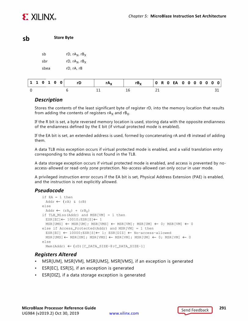
Chapter 5: MicroBlaze Instruction Set Architecture
sb Store Byte
sb rD, rAX, rBX
sbr rD, rAX, rBX
sbea rD, rA, rB
1 1 0 1 0 0 rD rAX rBX 0 R 0 EA 0 0 0 0 0 0 0
0 6 11 16 21 31
DescriptionStores the contents of the least significant byte of register rD, into the memory location that results from adding the contents of registers rAX and rBX.
If the R bit is set, a byte reversed memory location is used, storing data with the opposite endianness of the endianness defined by the E bit (if virtual protected mode is enabled).
If the EA bit is set, an extended address is used, formed by concatenating rA and rB instead of adding them.
A data TLB miss exception occurs if virtual protected mode is enabled, and a valid translation entry corresponding to the address is not found in the TLB.
A data storage exception occurs if virtual protected mode is enabled, and access is prevented by no-access-allowed or read-only zone protection. No-access-allowed can only occur in user mode.
A privileged instruction error occurs if the EA bit is set, Physical Address Extension (PAE) is enabled, and the instruction is not explicitly allowed.
Pseudocodeif EA = 1 thenAddr ← (rA) & (rB)
elseAddr ← (rAX) + (rBX)
if TLB_Miss(Addr) and MSR[VM] = 1 thenESR[EC]← 10010;ESR[S]← 1MSR[UMS] ← MSR[UM]; MSR[VMS] ← MSR[VM]; MSR[UM] ← 0; MSR[VM] ← 0
else if Access_Protected(Addr) and MSR[VM] = 1 thenESR[EC] ← 10000;ESR[S]← 1; ESR[DIZ] ← No-access-allowedMSR[UMS]← MSR[UM]; MSR[VMS] ← MSR[VM]; MSR[UM] ← 0; MSR[VM] ← 0
elseMem(Addr) ← (rD)[C_DATA_SIZE-8:C_DATA_SIZE-1]
Registers Altered• MSR[UM], MSR[VM], MSR[UMS], MSR[VMS], if an exception is generated• ESR[EC], ESR[S], if an exception is generated• ESR[DIZ], if a data storage exception is generated
MicroBlaze Processor Reference Guide 291UG984 (v2019.2) Oct 30, 2019 www.xilinx.com
Send Feedback

Chapter 5: MicroBlaze Instruction Set Architecture
Latency• 1 cycle with C_AREA_OPTIMIZED=0 or 2• 2 cycles with C_AREA_OPTIMIZED=1
NotesThe byte reversed instruction is only valid if MicroBlaze is configured to use reorder instructions (C_USE_REORDER_INSTR = 1).
The extended address instruction is only valid if MicroBlaze is configured to use extended address (C_ADDR_SIZE > 32) and is using 32-bit mode (C_DATA_SIZE = 32).
MicroBlaze Processor Reference Guide 292UG984 (v2019.2) Oct 30, 2019 www.xilinx.com
Send Feedback

Chapter 5: MicroBlaze Instruction Set Architecture
sbi Store Byte Immediate
sbi rD, rAX, IMM
1 1 1 1 0 0 rD rAX IMM
0 6 11 16 31
DescriptionStores the contents of the least significant byte of register rD, into the memory location that results from adding the contents of register rAX and the sign-extended IMM value.
A data TLB miss exception occurs if virtual protected mode is enabled, and a valid translation entry corresponding to the address is not found in the TLB.
A data storage exception occurs if virtual protected mode is enabled, and access is prevented by no-access-allowed or read-only zone protection. No-access-allowed can only occur in user mode.
PseudocodeAddr ← (rAX) + sext(IMM) if TLB_Miss(Addr) and MSR[VM] = 1 thenESR[EC]← 10010;ESR[S]← 1MSR[UMS] ← MSR[UM]; MSR[VMS] ← MSR[VM]; MSR[UM] ← 0; MSR[VM] ← 0
else if Access_Protected(Addr) and MSR[VM] = 1 thenESR[EC] ← 10000;ESR[S]← 1; ESR[DIZ] ← No-access-allowedMSR[UMS]← MSR[UM]; MSR[VMS] ← MSR[VM]; MSR[UM] ← 0; MSR[VM] ← 0
elseMem(Addr) ← (rD)[C_DATA_SIZE-8:C_DATA_SIZE-1]
Registers Altered• MSR[UM], MSR[VM], MSR[UMS], MSR[VMS], if an exception is generated• ESR[EC], ESR[S], if an exception is generated• ESR[DIZ], if a data storage exception is generated
Latency• 1 cycle with C_AREA_OPTIMIZED=0 or 2• 2 cycles with C_AREA_OPTIMIZED=1
NoteBy default, Type B store instructions will take the 16-bit IMM field value and sign extend it to use as the immediate operand. This behavior can be overridden by preceding the instruction with an imm or imml instruction. See the instructions “imm” and “imml” for details on using immediate values.
MicroBlaze Processor Reference Guide 293UG984 (v2019.2) Oct 30, 2019 www.xilinx.com
Send Feedback
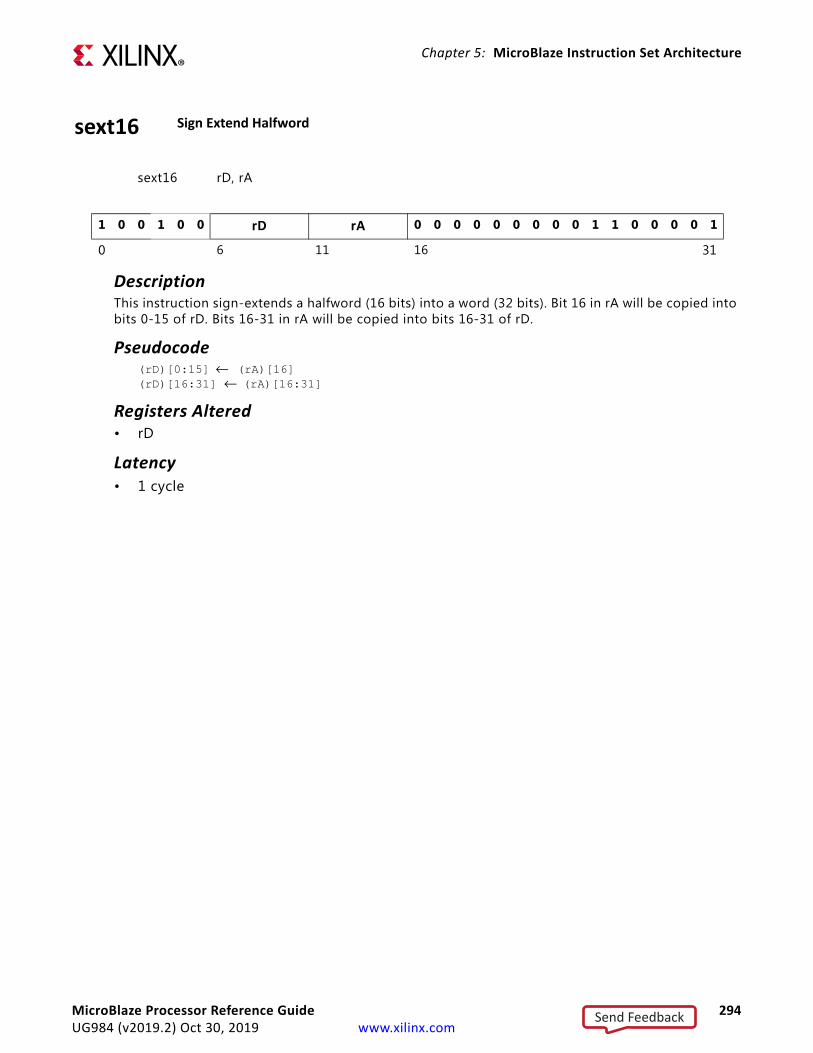
Chapter 5: MicroBlaze Instruction Set Architecture
sext16 Sign Extend Halfword
sext16 rD, rA
1 0 0 1 0 0 rD rA 0 0 0 0 0 0 0 0 0 1 1 0 0 0 0 1
0 6 11 16 31
DescriptionThis instruction sign-extends a halfword (16 bits) into a word (32 bits). Bit 16 in rA will be copied into bits 0-15 of rD. Bits 16-31 in rA will be copied into bits 16-31 of rD.
Pseudocode(rD)[0:15] ← (rA)[16] (rD)[16:31] ← (rA)[16:31]
Registers Altered• rD
Latency• 1 cycle
MicroBlaze Processor Reference Guide 294UG984 (v2019.2) Oct 30, 2019 www.xilinx.com
Send Feedback

Chapter 5: MicroBlaze Instruction Set Architecture
sext8 Sign Extend Byte
sext8 rD, rA
1 0 0 1 0 0 rD rA 0 0 0 0 0 0 0 0 0 1 1 0 0 0 0 0
0 6 11 16 31
DescriptionThis instruction sign-extends a byte (8 bits) into a word (32 bits). Bit 24 in rA will be copied into bits 0-23 of rD. Bits 24-31 in rA will be copied into bits 24-31 of rD.
Pseudocode(rD)[0:23] ← (rA)[24] (rD)[24:31] ← (rA)[24:31]
Registers Altered• rD
Latency• 1 cycle
MicroBlaze Processor Reference Guide 295UG984 (v2019.2) Oct 30, 2019 www.xilinx.com
Send Feedback
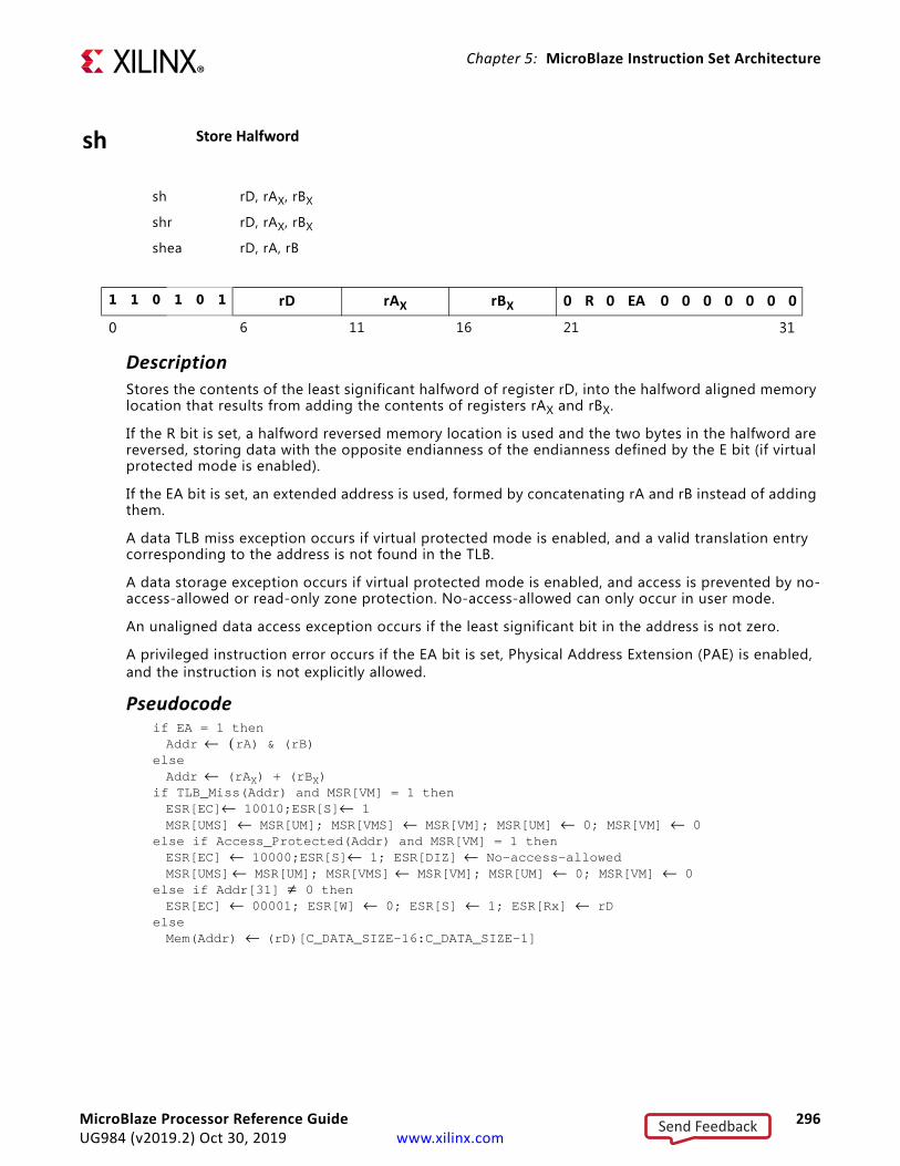
Chapter 5: MicroBlaze Instruction Set Architecture
sh Store Halfword
sh rD, rAX, rBX
shr rD, rAX, rBX
shea rD, rA, rB
1 1 0 1 0 1 rD rAX rBX 0 R 0 EA 0 0 0 0 0 0 0
0 6 11 16 21 31
DescriptionStores the contents of the least significant halfword of register rD, into the halfword aligned memory location that results from adding the contents of registers rAX and rBX.
If the R bit is set, a halfword reversed memory location is used and the two bytes in the halfword are reversed, storing data with the opposite endianness of the endianness defined by the E bit (if virtual protected mode is enabled).
If the EA bit is set, an extended address is used, formed by concatenating rA and rB instead of adding them.
A data TLB miss exception occurs if virtual protected mode is enabled, and a valid translation entry corresponding to the address is not found in the TLB.
A data storage exception occurs if virtual protected mode is enabled, and access is prevented by no-access-allowed or read-only zone protection. No-access-allowed can only occur in user mode.
An unaligned data access exception occurs if the least significant bit in the address is not zero.
A privileged instruction error occurs if the EA bit is set, Physical Address Extension (PAE) is enabled, and the instruction is not explicitly allowed.
Pseudocodeif EA = 1 thenAddr ← (rA) & (rB)
elseAddr ← (rAX) + (rBX)
if TLB_Miss(Addr) and MSR[VM] = 1 thenESR[EC]← 10010;ESR[S]← 1MSR[UMS] ← MSR[UM]; MSR[VMS] ← MSR[VM]; MSR[UM] ← 0; MSR[VM] ← 0
else if Access_Protected(Addr) and MSR[VM] = 1 thenESR[EC] ← 10000;ESR[S]← 1; ESR[DIZ] ← No-access-allowedMSR[UMS]← MSR[UM]; MSR[VMS] ← MSR[VM]; MSR[UM] ← 0; MSR[VM] ← 0
else if Addr[31] ≠ 0 thenESR[EC] ← 00001; ESR[W] ← 0; ESR[S] ← 1; ESR[Rx] ← rD
else Mem(Addr) ← (rD)[C_DATA_SIZE-16:C_DATA_SIZE-1]
MicroBlaze Processor Reference Guide 296UG984 (v2019.2) Oct 30, 2019 www.xilinx.com
Send Feedback
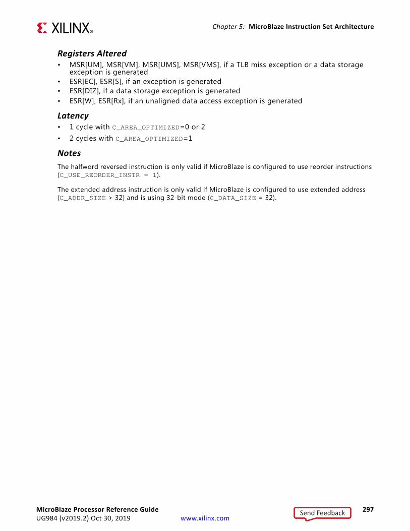
Chapter 5: MicroBlaze Instruction Set Architecture
Registers Altered• MSR[UM], MSR[VM], MSR[UMS], MSR[VMS], if a TLB miss exception or a data storage
exception is generated• ESR[EC], ESR[S], if an exception is generated• ESR[DIZ], if a data storage exception is generated• ESR[W], ESR[Rx], if an unaligned data access exception is generated
Latency• 1 cycle with C_AREA_OPTIMIZED=0 or 2• 2 cycles with C_AREA_OPTIMIZED=1
NotesThe halfword reversed instruction is only valid if MicroBlaze is configured to use reorder instructions (C_USE_REORDER_INSTR = 1).
The extended address instruction is only valid if MicroBlaze is configured to use extended address (C_ADDR_SIZE > 32) and is using 32-bit mode (C_DATA_SIZE = 32).
MicroBlaze Processor Reference Guide 297UG984 (v2019.2) Oct 30, 2019 www.xilinx.com
Send Feedback

Chapter 5: MicroBlaze Instruction Set Architecture
shi Store Halfword Immediate
shi rD, rAX, IMM
1 1 1 1 0 1 rD rAX IMM
0 6 11 16 31
DescriptionStores the contents of the least significant halfword of register rD, into the halfword aligned memory location that results from adding the contents of register rAX and the sign-extended IMM value.
A data TLB miss exception occurs if virtual protected mode is enabled, and a valid translation entry corresponding to the address is not found in the TLB. A data storage exception occurs if virtual protected mode is enabled, and access is prevented by no-access-allowed or read-only zone protection. No-access-allowed can only occur in user mode. An unaligned data access exception occurs if the least significant bit in the address is not zero.
PseudocodeAddr ← (rAX) + sext(IMM) if TLB_Miss(Addr) and MSR[VM] = 1 thenESR[EC]← 10010;ESR[S]← 1MSR[UMS] ← MSR[UM]; MSR[VMS] ← MSR[VM]; MSR[UM] ← 0; MSR[VM] ← 0
else if Access_Protected(Addr) and MSR[VM] = 1 thenESR[EC] ← 10000;ESR[S]← 1; ESR[DIZ] ← No-access-allowedMSR[UMS]← MSR[UM]; MSR[VMS] ← MSR[VM]; MSR[UM] ← 0; MSR[VM] ← 0
else if Addr[31] ≠ 0 thenESR[EC] ← 00001; ESR[W] ← 0; ESR[S] ← 1; ESR[Rx] ← rD
else Mem(Addr) ← (rD)[C_DATA_SIZE-16:C_DATA_SIZE-1]
Registers Altered• MSR[UM], MSR[VM], MSR[UMS], MSR[VMS], if a TLB miss exception or a data storage
exception is generated• ESR[EC], ESR[S], if an exception is generated• ESR[DIZ], if a data storage exception is generated• ESR[W], ESR[Rx], if an unaligned data access exception is generated
Latency• 1 cycle with C_AREA_OPTIMIZED=0 or 2• 2 cycles with C_AREA_OPTIMIZED=1
NoteBy default, Type B store instructions will take the 16-bit IMM field value and sign extend it to use as the immediate operand. This behavior can be overridden by preceding the instruction with an imm or imml instruction. See the instructions “imm” and “imml” for details on using immediate values.
MicroBlaze Processor Reference Guide 298UG984 (v2019.2) Oct 30, 2019 www.xilinx.com
Send Feedback

Chapter 5: MicroBlaze Instruction Set Architecture
sra Shift Right Arithmetic
sra rD, rA
1 0 0 1 0 0 rD rA 0 0 0 0 0 0 0 0 0 0 0 0 0 0 0 1
0 6 11 16 31
DescriptionShifts arithmetically the contents of register rA, one bit to the right, and places the result in rD. The most significant bit of rA (that is, the sign bit) placed in the most significant bit of rD. The least significant bit coming out of the shift chain is placed in the Carry flag.
Pseudocode(rD)[0] ← (rA)[0] (rD)[1:31] ← (rA)[0:30] MSR[C] ← (rA)[31]
Registers Altered• rD• MSR[C]
Latency• 1 cycle
MicroBlaze Processor Reference Guide 299UG984 (v2019.2) Oct 30, 2019 www.xilinx.com
Send Feedback

Chapter 5: MicroBlaze Instruction Set Architecture
src Shift Right with Carry
src rD, rA
1 0 0 1 0 0 rD rA 0 0 0 0 0 0 0 0 0 0 1 0 0 0 0 1
0 6 11 16 31
DescriptionShifts the contents of register rA, one bit to the right, and places the result in rD. The Carry flag is shifted in the shift chain and placed in the most significant bit of rD. The least significant bit coming out of the shift chain is placed in the Carry flag.
Pseudocode(rD)[0] ← MSR[C] (rD)[1:31] ← (rA)[0:30] MSR[C] ← (rA)[31]
Registers Altered• rD• MSR[C]
Latency• 1 cycle
MicroBlaze Processor Reference Guide 300UG984 (v2019.2) Oct 30, 2019 www.xilinx.com
Send Feedback

Chapter 5: MicroBlaze Instruction Set Architecture
srl Shift Right Logical
srl rD, rA
1 0 0 1 0 0 rD rA 0 0 0 0 0 0 0 0 0 1 0 0 0 0 0 1
0 6 11 16 31
DescriptionShifts logically the contents of register rA, one bit to the right, and places the result in rD. A zero is shifted in the shift chain and placed in the most significant bit of rD. The least significant bit coming out of the shift chain is placed in the Carry flag.
Pseudocode(rD)[0] ← 0 (rD)[1:31] ← (rA)[0:30] MSR[C] ← (rA)[31]
Registers Altered• rD• MSR[C]
Latency• 1 cycle
MicroBlaze Processor Reference Guide 301UG984 (v2019.2) Oct 30, 2019 www.xilinx.com
Send Feedback

Chapter 5: MicroBlaze Instruction Set Architecture
sw Store Word
sw rD, rAX, rBX
swr rD, rAX, rBX
swea rD, rA, rB
1 1 0 1 1 0 rD rAX rBX 0 R 0 EA 0 0 0 0 0 0 0
0 6 11 16 21 31
DescriptionStores the contents of register rD, into the word aligned memory location that results from adding the contents of registers rAX and rBX.
If the R bit is set, the bytes in the stored word are reversed , storing data with the opposite endianness of the endianness defined by the E bit (if virtual protected mode is enabled).
If the EA bit is set, an extended address is used, formed by concatenating rA and rB instead of adding them.
A data TLB miss exception occurs if virtual protected mode is enabled, and a valid translation entry corresponding to the address is not found in the TLB.
A data storage exception occurs if virtual protected mode is enabled, and access is prevented by no-access-allowed or read-only zone protection. No-access-allowed can only occur in user mode.
An unaligned data access exception occurs if the two least significant bits in the address are not zero.
A privileged instruction error occurs if the EA bit is set, Physical Address Extension (PAE) is enabled, and the instruction is not explicitly allowed.
Pseudocodeif EA = 1 thenAddr ← (rA) & (rB)
elseAddr ← (rAX) + (rBX)
if TLB_Miss(Addr) and MSR[VM] = 1 thenESR[EC]← 10010;ESR[S]← 1MSR[UMS] ← MSR[UM]; MSR[VMS] ← MSR[VM]; MSR[UM] ← 0; MSR[VM] ← 0
else if Access_Protected(Addr) and MSR[VM] = 1 thenESR[EC] ← 10000;ESR[S]← 1; ESR[DIZ] ← No-access-allowedMSR[UMS]← MSR[UM]; MSR[VMS] ← MSR[VM]; MSR[UM] ← 0; MSR[VM] ← 0
else if Addr[30:31] ≠ 0 thenESR[EC] ← 00001; ESR[W] ← 1; ESR[S] ← 1; ESR[Rx] ← rD
else Mem(Addr) ← (rD)
MicroBlaze Processor Reference Guide 302UG984 (v2019.2) Oct 30, 2019 www.xilinx.com
Send Feedback
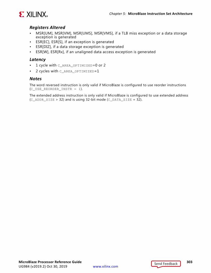
Chapter 5: MicroBlaze Instruction Set Architecture
Registers Altered• MSR[UM], MSR[VM], MSR[UMS], MSR[VMS], if a TLB miss exception or a data storage
exception is generated• ESR[EC], ESR[S], if an exception is generated• ESR[DIZ], if a data storage exception is generated• ESR[W], ESR[Rx], if an unaligned data access exception is generated
Latency• 1 cycle with C_AREA_OPTIMIZED=0 or 2• 2 cycles with C_AREA_OPTIMIZED=1
NotesThe word reversed instruction is only valid if MicroBlaze is configured to use reorder instructions (C_USE_REORDER_INSTR = 1).
The extended address instruction is only valid if MicroBlaze is configured to use extended address (C_ADDR_SIZE > 32) and is using 32-bit mode (C_DATA_SIZE = 32).
MicroBlaze Processor Reference Guide 303UG984 (v2019.2) Oct 30, 2019 www.xilinx.com
Send Feedback

Chapter 5: MicroBlaze Instruction Set Architecture
swapb Swap Bytes
swapb rD, rA
1 0 0 1 0 0 rD rA 0 0 0 0 0 0 0 1 1 1 1 0 0 0 0 0
0 6 11 16 31
DescriptionSwaps the contents of register rA treated as four bytes, and places the result in rD. This effectively converts the byte sequence in the register between endianness formats, either from little-endian to big-endian or vice versa.
Pseudocode(rD)[24:31] ← (rA)[0:7] (rD)[16:23] ← (rA)[8:15] (rD)[8:15] ← (rA)[16:23] (rD)[0:7] ← (rA)[24:31]
Registers Altered• rD
Latency• 1 cycle
NoteThis instruction is only valid if MicroBlaze is configured to use reorder instructions (C_USE_REORDER_INSTR = 1).
MicroBlaze Processor Reference Guide 304UG984 (v2019.2) Oct 30, 2019 www.xilinx.com
Send Feedback
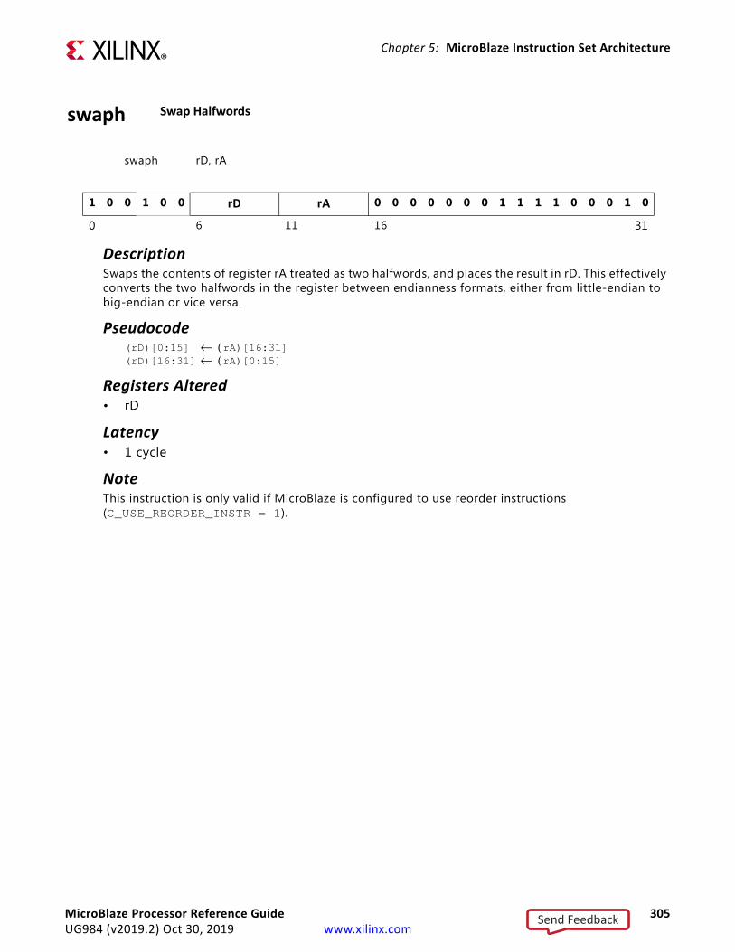
Chapter 5: MicroBlaze Instruction Set Architecture
swaph Swap Halfwords
swaph rD, rA
1 0 0 1 0 0 rD rA 0 0 0 0 0 0 0 1 1 1 1 0 0 0 1 0
0 6 11 16 31
DescriptionSwaps the contents of register rA treated as two halfwords, and places the result in rD. This effectively converts the two halfwords in the register between endianness formats, either from little-endian to big-endian or vice versa.
Pseudocode(rD)[0:15] ← (rA)[16:31] (rD)[16:31] ← (rA)[0:15]
Registers Altered• rD
Latency• 1 cycle
NoteThis instruction is only valid if MicroBlaze is configured to use reorder instructions (C_USE_REORDER_INSTR = 1).
MicroBlaze Processor Reference Guide 305UG984 (v2019.2) Oct 30, 2019 www.xilinx.com
Send Feedback

Chapter 5: MicroBlaze Instruction Set Architecture
swi Store Word Immediate
swi rD, rAX, IMM
1 1 1 1 1 0 rD rAX IMM
0 6 11 16 31
DescriptionStores the contents of register rD, into the word aligned memory location that results from adding the contents of registers rAX and the sign-extended IMM value.
A data TLB miss exception occurs if virtual protected mode is enabled, and a valid translation entry corresponding to the address is not found in the TLB.
A data storage exception occurs if virtual protected mode is enabled, and access is prevented by no-access-allowed or read-only zone protection. No-access-allowed can only occur in user mode.
An unaligned data access exception occurs if the two least significant bits in the address are not zero.
PseudocodeAddr ← (rAX) + sext(IMM) if TLB_Miss(Addr) and MSR[VM] = 1 thenESR[EC]← 10010;ESR[S]← 1MSR[UMS] ← MSR[UM]; MSR[VMS] ← MSR[VM]; MSR[UM] ← 0; MSR[VM] ← 0
else if Access_Protected(Addr) and MSR[VM] = 1 thenESR[EC] ← 10000;ESR[S]← 1; ESR[DIZ] ← No-access-allowedMSR[UMS]← MSR[UM]; MSR[VMS] ← MSR[VM]; MSR[UM] ← 0; MSR[VM] ← 0
else if Addr[30:31] ≠ 0 thenESR[EC] ← 00001; ESR[W] ← 1; ESR[S] ← 1; ESR[Rx] ← rD
else Mem(Addr) ← (rD)
Registers Altered• MSR[UM], MSR[VM], MSR[UMS], MSR[VMS], if a TLB miss exception or a data storage
exception is generated• ESR[EC], ESR[S], if an exception is generated• ESR[DIZ], if a data storage exception is generated• ESR[W], ESR[Rx], if an unaligned data access exception is generated
Latency• 1 cycle with C_AREA_OPTIMIZED=0 or 2• 2 cycles with C_AREA_OPTIMIZED=1
NoteBy default, Type B store instructions will take the 16-bit IMM field value and sign extend it to use as the immediate operand. This behavior can be overridden by preceding the instruction with an imm or imml instruction. See the instructions “imm” and “imml” for details on using immediate values.
MicroBlaze Processor Reference Guide 306UG984 (v2019.2) Oct 30, 2019 www.xilinx.com
Send Feedback

Chapter 5: MicroBlaze Instruction Set Architecture
swx Store Word Exclusive
swx rD, rA, rB
1 1 0 1 1 0 rD rA rB 1 0 0 0 0 0 0 0 0 0 0
0 6 11 16 21 31
DescriptionConditionally stores the contents of register rD, into the word aligned memory location that results from adding the contents of registers rA and rB. If an AXI4 interconnect with exclusive access enabled is used, the store occurs if the interconnect response is EXOKAY, and the reservation bit is set; otherwise the store occurs when the reservation bit is set. The carry flag (MSR[C]) is set if the store does not occur, otherwise it is cleared. The reservation bit is cleared.
A data TLB miss exception occurs if virtual protected mode is enabled, and a valid translation entry corresponding to the address is not found in the TLB.
A data storage exception occurs if virtual protected mode is enabled, and access is prevented by no-access-allowed or read-only zone protection. No-access-allowed can only occur in user mode.
An unaligned data access exception will not occur even if the two least significant bits in the address are not zero.
Enabling AXI exclusive access ensures that the operation is protected from other bus masters, but requires that the addressed slave supports exclusive access. When exclusive access is not enabled, only the internal reservation bit is used. Exclusive access is enabled using the two parameters C_M_AXI_DP_EXCLUSIVE_ACCESS and C_M_AXI_DC_EXCLUSIVE_ACCESS for the peripheral and cache interconnect, respectively.
PseudocodeAddr ← (rA) + (rB) if Reservation = 0 thenMSR[C] ← 1
else if TLB_Miss(Addr) and MSR[VM] = 1 thenESR[EC]← 10010;ESR[S]← 1MSR[UMS] ← MSR[UM]; MSR[VMS] ← MSR[VM]; MSR[UM] ← 0; MSR[VM] ← 0
else if Access_Protected(Addr) and MSR[VM] = 1 thenESR[EC] ← 10000;ESR[S]← 1; ESR[DIZ] ← No-access-allowedMSR[UMS]← MSR[UM]; MSR[VMS] ← MSR[VM]; MSR[UM] ← 0; MSR[VM] ← 0
elseReservation ← 0if AXI_Exclusive(Addr) and AXI_Response ≠ EXOKAY then MSR[C] ← 1
elseMem(Addr) ← (rD)[0:31]MSR[C] ← 0
MicroBlaze Processor Reference Guide 307UG984 (v2019.2) Oct 30, 2019 www.xilinx.com
Send Feedback
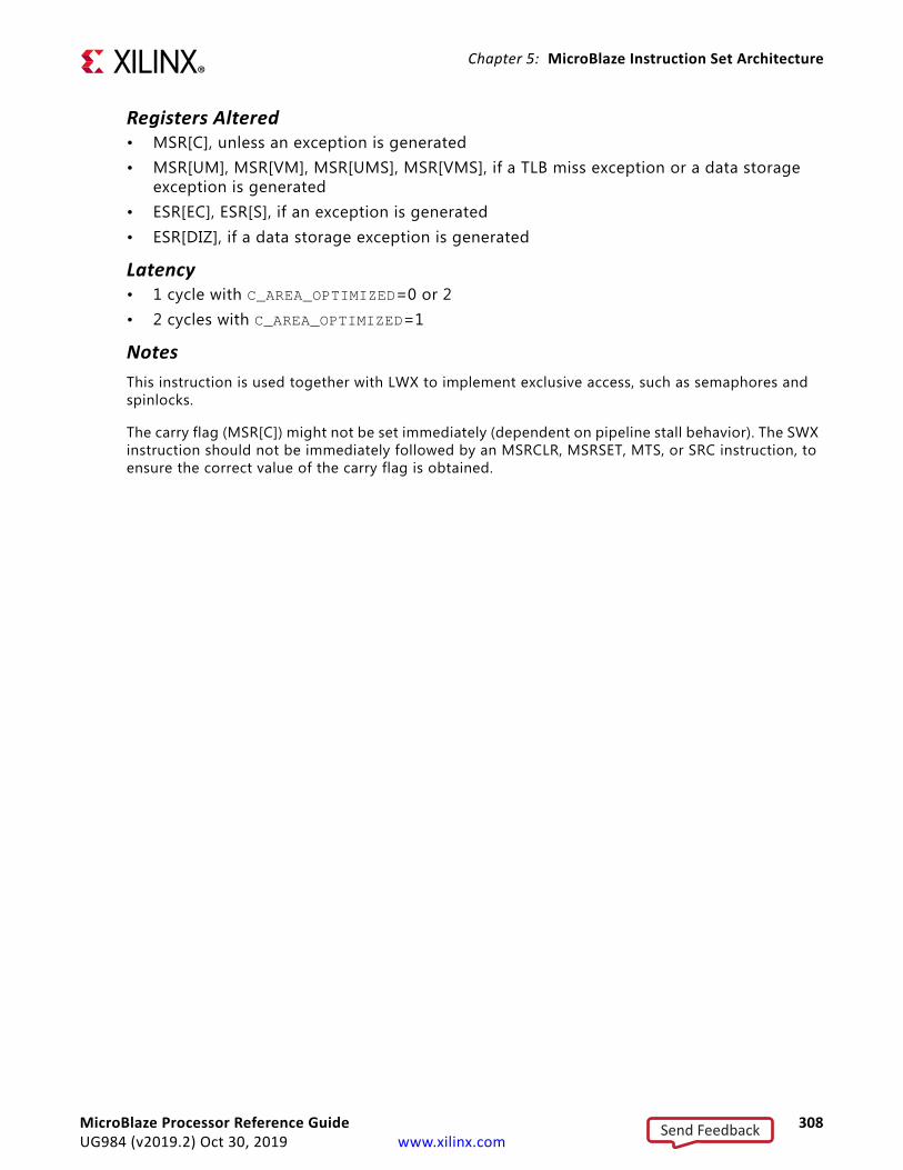
Chapter 5: MicroBlaze Instruction Set Architecture
Registers Altered• MSR[C], unless an exception is generated• MSR[UM], MSR[VM], MSR[UMS], MSR[VMS], if a TLB miss exception or a data storage
exception is generated• ESR[EC], ESR[S], if an exception is generated• ESR[DIZ], if a data storage exception is generated
Latency• 1 cycle with C_AREA_OPTIMIZED=0 or 2• 2 cycles with C_AREA_OPTIMIZED=1
NotesThis instruction is used together with LWX to implement exclusive access, such as semaphores and spinlocks.
The carry flag (MSR[C]) might not be set immediately (dependent on pipeline stall behavior). The SWX instruction should not be immediately followed by an MSRCLR, MSRSET, MTS, or SRC instruction, to ensure the correct value of the carry flag is obtained.
MicroBlaze Processor Reference Guide 308UG984 (v2019.2) Oct 30, 2019 www.xilinx.com
Send Feedback
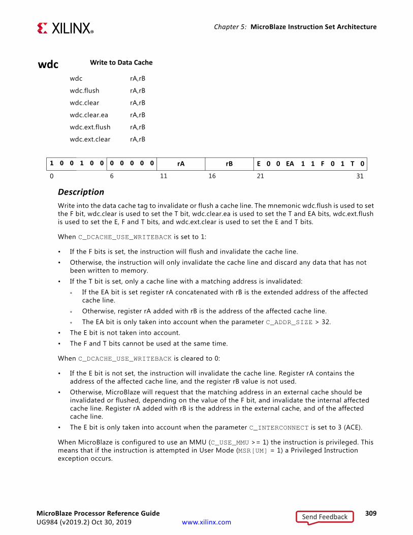
Chapter 5: MicroBlaze Instruction Set Architecture
wdc Write to Data Cache
wdc rA,rB
wdc.flush rA,rB
wdc.clear rA,rB
wdc.clear.ea rA,rB
wdc.ext.flush rA,rB
wdc.ext.clear rA,rB
1 0 0 1 0 0 0 0 0 0 0 rA rB E 0 0 EA 1 1 F 0 1 T 0
0 6 11 16 21 31
DescriptionWrite into the data cache tag to invalidate or flush a cache line. The mnemonic wdc.flush is used to set the F bit, wdc.clear is used to set the T bit, wdc.clear.ea is used to set the T and EA bits, wdc.ext.flush is used to set the E, F and T bits, and wdc.ext.clear is used to set the E and T bits.
When C_DCACHE_USE_WRITEBACK is set to 1:
• If the F bits is set, the instruction will flush and invalidate the cache line.• Otherwise, the instruction will only invalidate the cache line and discard any data that has not
been written to memory.• If the T bit is set, only a cache line with a matching address is invalidated:
° If the EA bit is set register rA concatenated with rB is the extended address of the affected cache line.
° Otherwise, register rA added with rB is the address of the affected cache line.
° The EA bit is only taken into account when the parameter C_ADDR_SIZE > 32.• The E bit is not taken into account.• The F and T bits cannot be used at the same time.
When C_DCACHE_USE_WRITEBACK is cleared to 0:
• If the E bit is not set, the instruction will invalidate the cache line. Register rA contains the address of the affected cache line, and the register rB value is not used.
• Otherwise, MicroBlaze will request that the matching address in an external cache should be invalidated or flushed, depending on the value of the F bit, and invalidate the internal affected cache line. Register rA added with rB is the address in the external cache, and of the affected cache line.
• The E bit is only taken into account when the parameter C_INTERCONNECT is set to 3 (ACE).
When MicroBlaze is configured to use an MMU (C_USE_MMU >= 1) the instruction is privileged. This means that if the instruction is attempted in User Mode (MSR[UM] = 1) a Privileged Instruction exception occurs.
MicroBlaze Processor Reference Guide 309UG984 (v2019.2) Oct 30, 2019 www.xilinx.com
Send Feedback

Chapter 5: MicroBlaze Instruction Set Architecture
Pseudocodeif MSR[UM] = 1 thenESR[EC] ← 00111
elseif C_DCACHE_USE_WRITEBACK = 1 thenif T = 1 and EA = 1 thenaddress ← (rA) & (rB)
elseaddress ← (rA) + (rB)
else if E = 0 thenaddress ← (rA)
elseaddress ← (rA) + (rB)
if C_DCACHE_LINE_LEN = 4 thencacheline_mask ← (1 << log2(C_DCACHE_BYTE_SIZE) - 4) - 1cacheline ← (DCache Line)[(address >> 4) ∧ cacheline_mask]cacheline_addr ← address & 0xfffffff0
if C_DCACHE_LINE_LEN = 8 thencacheline_mask ← (1 << log2(C_DCACHE_BYTE_SIZE) - 5) - 1cacheline ← (DCache Line)[(address >> 5) ∧ cacheline_mask]cacheline_addr ← address & 0xffffffe0
if C_DCACHE_LINE_LEN = 16 thencacheline_mask ← (1 << log2(C_DCACHE_BYTE_SIZE) - 6) - 1cacheline ← (DCache Line)[(address >> 6) ∧ cacheline_mask] cacheline_addr ← address & 0xffffffc0
if E = 0 and F = 1 and cacheline.Dirty thenfor i = 0 .. C_DCACHE_LINE_LEN - 1 loopif cacheline.Valid[i] thenMem(cacheline_addr + i * 4) ← cacheline.Data[i]
if T = 0 or C_DCACHE_USE_WRITEBACK = 0 thencacheline.Tag ← 0
else if cacheline.Address = cacheline_addr thencacheline.Tag ← 0
if E = 1 then if F = 1 thenrequest external cache flush with address
elserequest external cache invalidate with address
Registers Altered• ESR[EC], in case a privileged instruction exception is generated
Latency• 2 cycles for wdc.clear• 2 cycles for wdc with C_AREA_OPTIMIZED=0 or 2• 3 cycles for wdc with C_AREA_OPTIMIZED=0• 2 + N cycles for wdc.flush, where N is the number of clock cycles required to flush the
cache line to memory when necessary
MicroBlaze Processor Reference Guide 310UG984 (v2019.2) Oct 30, 2019 www.xilinx.com
Send Feedback
Chapter 5: MicroBlaze Instruction Set Architecture
NotesThe wdc, wdc.flush, wdc.clear and wdc.clear.ea instructions are independent of data cache enable (MSR[DCE]), and can be used either with the data cache enabled or disabled.
The wdc.clear and wdc.clear.ea instructions are intended to invalidate a specific area in memory, for example a buffer to be written by a Direct Memory Access device.
Using this instruction ensures that other cache lines are not inadvertently invalidated, erroneously discarding data that has not yet been written to memory.
The address of the affected cache line is always the physical address, independent of the parameter C_USE_MMU and whether the MMU is in virtual mode or real mode.
When using wdc.flush in a loop to flush the entire cache, the loop can be optimized by using rA as the cache base address and rB as the loop counter:
addik r5,r0,C_DCACHE_BASEADDRaddik r6,r0,C_DCACHE_BYTE_SIZE-C_DCACHE_LINE_LEN*4
loop: wdc.flush r5,r6bgtid r6,loopaddik r6,r6,-C_DCACHE_LINE_LEN*4
When using wdc.clear in a loop to invalidate a memory area in the cache, the loop can be optimized by using rA as the memory area base address and rB as the loop counter:
addik r5,r0,memory_area_base_addressaddik r6,r0,memory_area_byte_size-C_DCACHE_LINE_LEN*4
loop: wdc.clear r5,r6bgtid r6,loop
addik r6,r6,-C_DCACHE_LINE_LEN*4
MicroBlaze Processor Reference Guide 311UG984 (v2019.2) Oct 30, 2019 www.xilinx.com
Send Feedback

Chapter 5: MicroBlaze Instruction Set Architecture
wic Write to Instruction Cache
wic rA,rB
1 0 0 1 0 0 0 0 0 0 0 rA rB 0 0 0 0 1 1 0 1 0 0 0
0 6 11 16 21 31
DescriptionWrite into the instruction cache tag to invalidate a cache line. The register rB value is not used. Register rA contains the address of the affected cache line.
When MicroBlaze is configured to use an MMU (C_USE_MMU >= 1) this instruction is privileged. This means that if the instruction is attempted in User Mode (MSR[UM] = 1) a Privileged Instruction exception occurs.
Pseudocodeif MSR[UM] = 1 thenESR[EC] ← 00111
elseif C_ICACHE_LINE_LEN = 4 thencacheline_mask ← (1 << log2(C_CACHE_BYTE_SIZE) - 4) - 1(ICache Line)[((Ra) >> 4) ∧ cacheline_mask].Tag ← 0
if C_ICACHE_LINE_LEN = 8 thencacheline_mask ← (1 << log2(C_CACHE_BYTE_SIZE) - 5) - 1(ICache Line)[((Ra) >> 5) ∧ cacheline_mask].Tag ← 0
if C_ICACHE_LINE_LEN = 16 thencacheline_mask ← (1 << log2(C_CACHE_BYTE_SIZE) - 6) - 1(ICache Line)[((Ra) >> 6) ∧ cacheline_mask].Tag ← 0
Registers Altered• ESR[EC], in case a privileged instruction exception is generated
Latency• 2 cycles
NotesThe WIC instruction is independent of instruction cache enable (MSR[ICE]), and can be used either with the instruction cache enabled or disabled.
The address of the affected cache line is the virtual address when the parameter C_USE_MMU = 3 (VIRTUAL) and the MMU is in virtual mode, otherwise it is the physical address.
MicroBlaze Processor Reference Guide 312UG984 (v2019.2) Oct 30, 2019 www.xilinx.com
Send Feedback

Chapter 5: MicroBlaze Instruction Set Architecture
xor Logical Exclusive OR
xor rD, rA, rB
1 0 0 0 1 0 rD rA rB 0 0 0 0 0 0 0 0 0 0 0
0 6 11 16 21 31
DescriptionThe contents of register rA are XORed with the contents of register rB; the result is placed into register rD.
Pseudocode(rD) ← (rA) ⊕ (rB)
Registers Altered• rD
Latency• 1 cycle
MicroBlaze Processor Reference Guide 313UG984 (v2019.2) Oct 30, 2019 www.xilinx.com
Send Feedback

Chapter 5: MicroBlaze Instruction Set Architecture
xori Logical Exclusive OR with Immediate
xori rD, rA, IMM
1 0 1 0 1 0 rD rA IMM
0 6 11 16 31
DescriptionThe IMM field is extended to 32 bits by concatenating 16 0-bits on the left. The contents of register rA are XOR’ed with the extended IMM field; the result is placed into register rD.
Pseudocode(rD) ← (rA) ⊕ sext(IMM)
Registers Altered• rD
Latency• 1 cycle
NotesBy default, Type B Instructions will take the 16-bit IMM field value and sign extend it to 32 bits to use as the immediate operand. This behavior can be overridden by preceding the Type B instruction with an imm instruction. See the instruction “imm” for details on using 32-bit immediate values.
When this instruction is used with rD set to r0, a program trace event is emitted with the 14 least significant bits of the result. Typically this is used to trace operating system events like context switches and system calls, but it can be used by any program to trace significant events. The functionality is enabled by setting C_DEBUG_ENABLED = 2 (Extended) and C_DEBUG_TRACE_SIZE > 0. See “Program and Event Trace” in Chapter 2 for further details.
MicroBlaze Processor Reference Guide 314UG984 (v2019.2) Oct 30, 2019 www.xilinx.com
Send Feedback
Chapter 5: MicroBlaze Instruction Set Architecture
MicroBlaze 64-bit InstructionsAll additional instructions included in the instruction set for 64-bit MicroBlaze are defined in this section.
These instructions use the full 64-bit register size to provide long arithmetic and logical operations.
All Type B 64-bit arithmetic and logical instructions must be preceded by an imml instruction, to indicate that they are 64-bit instructions. See the instruction “imml” for details on using 64-bit immediate values.
The extended instruction set also defines double precision floating point instructions.
MicroBlaze Processor Reference Guide 315UG984 (v2019.2) Oct 30, 2019 www.xilinx.com
Send Feedback

Chapter 5: MicroBlaze Instruction Set Architecture
addl Arithmetic Add Long
addl rDL, rAL, rBL Add Long
addlc rDL, rAL, rBL Add Long with Carry
addlk rDL, rAL, rBL Add Long and Keep Carry
addlkc rDL, rAL, rBL Add Long with Carry and Keep Carry
0 0 0 K C 0 rDL rAL rBL 0 0 1 0 0 0 0 0 0 0 0
0 6 11 16 21 31
DescriptionThe sum of the contents of registers rAL and rBL, is placed into register rDL.
Bit 3 of the instruction (labeled as K in the figure) is set to one for the mnemonic addlk. Bit 4 of the instruction (labeled as C in the figure) is set to one for the mnemonic addlc. Both bits are set to one for the mnemonic addlkc.
When an add instruction has bit 3 set (addlk, addlkc), the carry flag will Keep its previous value regardless of the outcome of the execution of the instruction. If bit 3 is cleared (addl, addlc), then the carry flag will be affected by the execution of the instruction.
When bit 4 of the instruction is set to one (addlc, addlkc), the content of the carry flag (MSR[C]) affects the execution of the instruction. When bit 4 is cleared (addl, addlk), the content of the carry flag does not affect the execution of the instruction (providing a normal addition).
Pseudocodeif C = 0 then(rDL) ← (rAL) + (rBL)
else(rDL) ← (rAL) + (rBL) + MSR[C]
if K = 0 thenMSR[C] ← CarryOut64
Registers Altered• rDL
• MSR[C]
Latency1 cycle
NotesThe C bit in the instruction opcode is not the same as the carry bit in the MSR.
MicroBlaze Processor Reference Guide 316UG984 (v2019.2) Oct 30, 2019 www.xilinx.com
Send Feedback
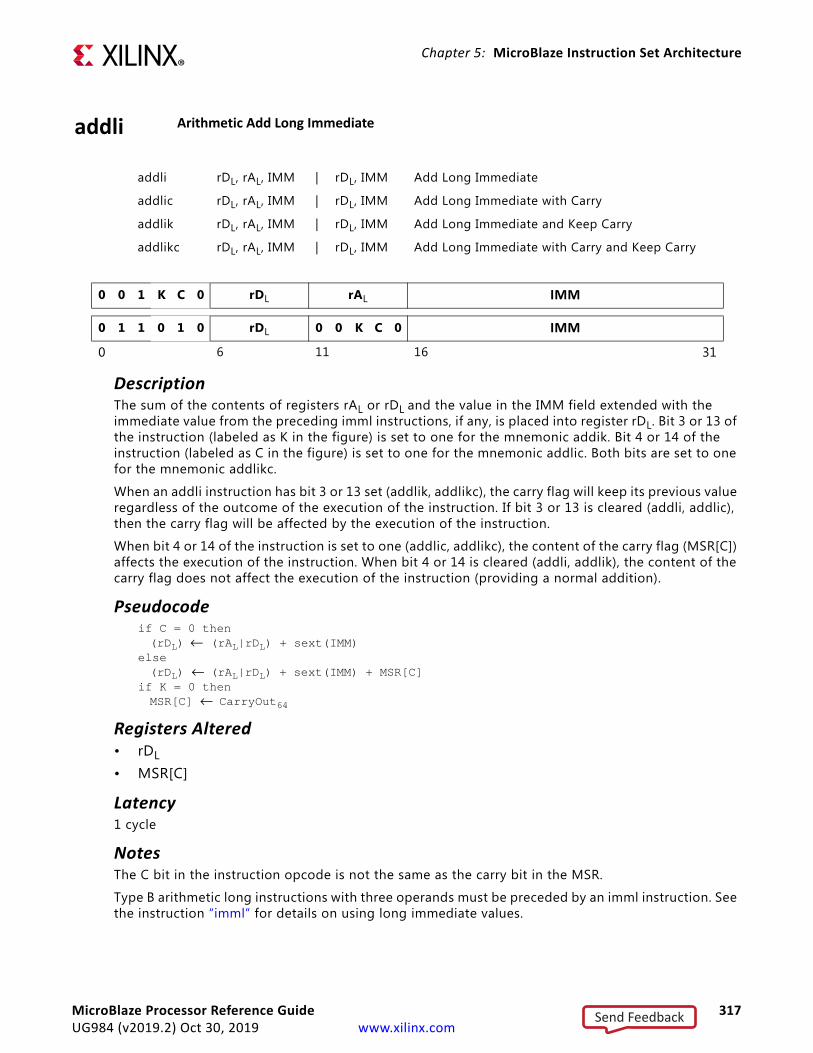
Chapter 5: MicroBlaze Instruction Set Architecture
addli Arithmetic Add Long Immediate
addli rDL, rAL, IMM | rDL, IMM Add Long Immediate
addlic rDL, rAL, IMM | rDL, IMM Add Long Immediate with Carry
addlik rDL, rAL, IMM | rDL, IMM Add Long Immediate and Keep Carry
addlikc rDL, rAL, IMM | rDL, IMM Add Long Immediate with Carry and Keep Carry
0 0 1 K C 0 rDL rAL IMM
0 1 1 0 1 0 rDL 0 0 K C 0 IMM
0 6 11 16 31
DescriptionThe sum of the contents of registers rAL or rDL and the value in the IMM field extended with the immediate value from the preceding imml instructions, if any, is placed into register rDL. Bit 3 or 13 of the instruction (labeled as K in the figure) is set to one for the mnemonic addik. Bit 4 or 14 of the instruction (labeled as C in the figure) is set to one for the mnemonic addlic. Both bits are set to one for the mnemonic addlikc.
When an addli instruction has bit 3 or 13 set (addlik, addlikc), the carry flag will keep its previous value regardless of the outcome of the execution of the instruction. If bit 3 or 13 is cleared (addli, addlic), then the carry flag will be affected by the execution of the instruction.
When bit 4 or 14 of the instruction is set to one (addlic, addlikc), the content of the carry flag (MSR[C]) affects the execution of the instruction. When bit 4 or 14 is cleared (addli, addlik), the content of the carry flag does not affect the execution of the instruction (providing a normal addition).
Pseudocodeif C = 0 then(rDL) ← (rAL|rDL) + sext(IMM)
else(rDL) ← (rAL|rDL) + sext(IMM) + MSR[C]
if K = 0 thenMSR[C] ← CarryOut64
Registers Altered• rDL• MSR[C]
Latency1 cycle
NotesThe C bit in the instruction opcode is not the same as the carry bit in the MSR.
Type B arithmetic long instructions with three operands must be preceded by an imml instruction. See the instruction “imml” for details on using long immediate values.
MicroBlaze Processor Reference Guide 317UG984 (v2019.2) Oct 30, 2019 www.xilinx.com
Send Feedback
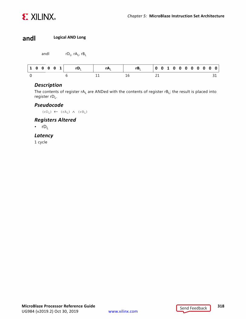
Chapter 5: MicroBlaze Instruction Set Architecture
andl Logical AND Long
andl rDL, rAL, rBL
1 0 0 0 0 1 rDL rAL rBL 0 0 1 0 0 0 0 0 0 0 0
0 6 11 16 21 31
DescriptionThe contents of register rAL are ANDed with the contents of register rBL; the result is placed into register rDL.
Pseudocode(rDL) ← (rAL) ∧ (rBL)
Registers Altered• rDL
Latency1 cycle
MicroBlaze Processor Reference Guide 318UG984 (v2019.2) Oct 30, 2019 www.xilinx.com
Send Feedback
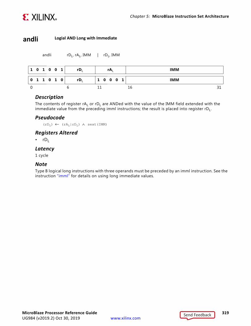
Chapter 5: MicroBlaze Instruction Set Architecture
andli Logial AND Long with Immediate
andli rDL, rAL, IMM | rDL, IMM
1 0 1 0 0 1 rDL rAL IMM
0 1 1 0 1 0 rDL 1 0 0 0 1 IMM
0 6 11 16 31
DescriptionThe contents of register rAL or rDL are ANDed with the value of the IMM field extended with the immediate value from the preceding imml instructions; the result is placed into register rDL.
Pseudocode(rDL) ← (rAL|rDL) ∧ sext(IMM)
Registers Altered• rDL
Latency1 cycle
NoteType B logical long instructions with three operands must be preceded by an imml instruction. See the instruction “imml” for details on using long immediate values.
MicroBlaze Processor Reference Guide 319UG984 (v2019.2) Oct 30, 2019 www.xilinx.com
Send Feedback
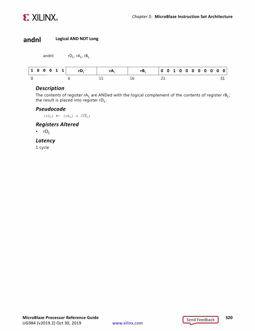
Chapter 5: MicroBlaze Instruction Set Architecture
andnl Logical AND NOT Long
andnl rDL, rAL, rBL
1 0 0 0 1 1 rDL rAL rBL 0 0 1 0 0 0 0 0 0 0 0
0 6 11 16 21 31
DescriptionThe contents of register rAL are ANDed with the logical complement of the contents of register rBL; the result is placed into register rDL.
Pseudocode(rDL) ← (rAL) ∧ (rBL)
Registers Altered• rDL
Latency1 cycle
MicroBlaze Processor Reference Guide 320UG984 (v2019.2) Oct 30, 2019 www.xilinx.com
Send Feedback
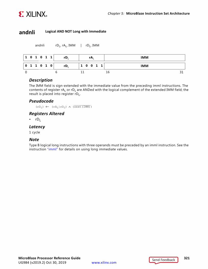
Chapter 5: MicroBlaze Instruction Set Architecture
andnli Logical AND NOT Long with Immediate
andnli rDL, rAL, IMM | rDL, IMM
1 0 1 0 1 1 rDL rAL IMM
0 1 1 0 1 0 rDL 1 0 0 1 1 IMM
0 6 11 16 31
DescriptionThe IMM field is sign-extended with the immediate value from the preceding imml instructions. The contents of register rAL or rDL are ANDed with the logical complement of the extended IMM field; the result is placed into register rDL.
Pseudocode(rDL) ← (rAL|rDL) ∧ (sext(IMM))
Registers Altered• rDL
Latency1 cycle
NoteType B logical long instructions with three operands must be preceded by an imml instruction. See the instruction “imml” for details on using long immediate values.
MicroBlaze Processor Reference Guide 321UG984 (v2019.2) Oct 30, 2019 www.xilinx.com
Send Feedback

Chapter 5: MicroBlaze Instruction Set Architecture
beaeq Branch Extended Address if Equal
beaeq rA, rBL Branch Extended Address if Equal
bealeq rAL, rBL Branch Extended Address if Long Equal
beaeqd rA, rBL Branch Extended Address if Equal with Delay
bealeqd rAL, rBL Branch Extended Address if Long Equal with Delay
1 0 0 1 1 1 D 1 0 0 0 rAL rBL 0 0 L 0 0 0 0 0 0 0 0
0 6 11 16 21 31
DescriptionBranch if rA or rAL is equal to 0, to the instruction located in the offset value of rBL. The target of the branch will be the instruction at address PC + rBL.
The mnemonics bealeq and bealeqd will set the L bit. If the L bit is set, a long comparison using rAL is performed, otherwise a 32-bit comparison using rA is performed.
The mnemonics beaeqd and bealeqd will set the D bit. The D bit determines whether there is a branch delay slot or not. If the D bit is set, it means that there is a delay slot and the instruction following the branch (that is, in the branch delay slot) is allowed to complete execution before executing the target instruction. If the D bit is not set, it means that there is no delay slot, so the instruction to be executed after the branch is the target instruction.
Pseudocodeif L = 1 and rAL = 0 then PC ← PC + rBL
else if rA = 0 then PC ← PC + rBL
else PC ← PC + 4
if D = 1 then allow following instruction to complete execution
Registers Altered• PC
Latency• 1 cycle (if branch is not taken)• 2 cycles (if branch is taken and the D bit is set)• 3 cycles (if branch is taken and the D bit is not set)
NoteA delay slot must not be used by the following: imm, imml, branch, or break instructions. Interrupts and external hardware breaks are deferred until after the delay slot branch has been completed.
MicroBlaze Processor Reference Guide 322UG984 (v2019.2) Oct 30, 2019 www.xilinx.com
Send Feedback
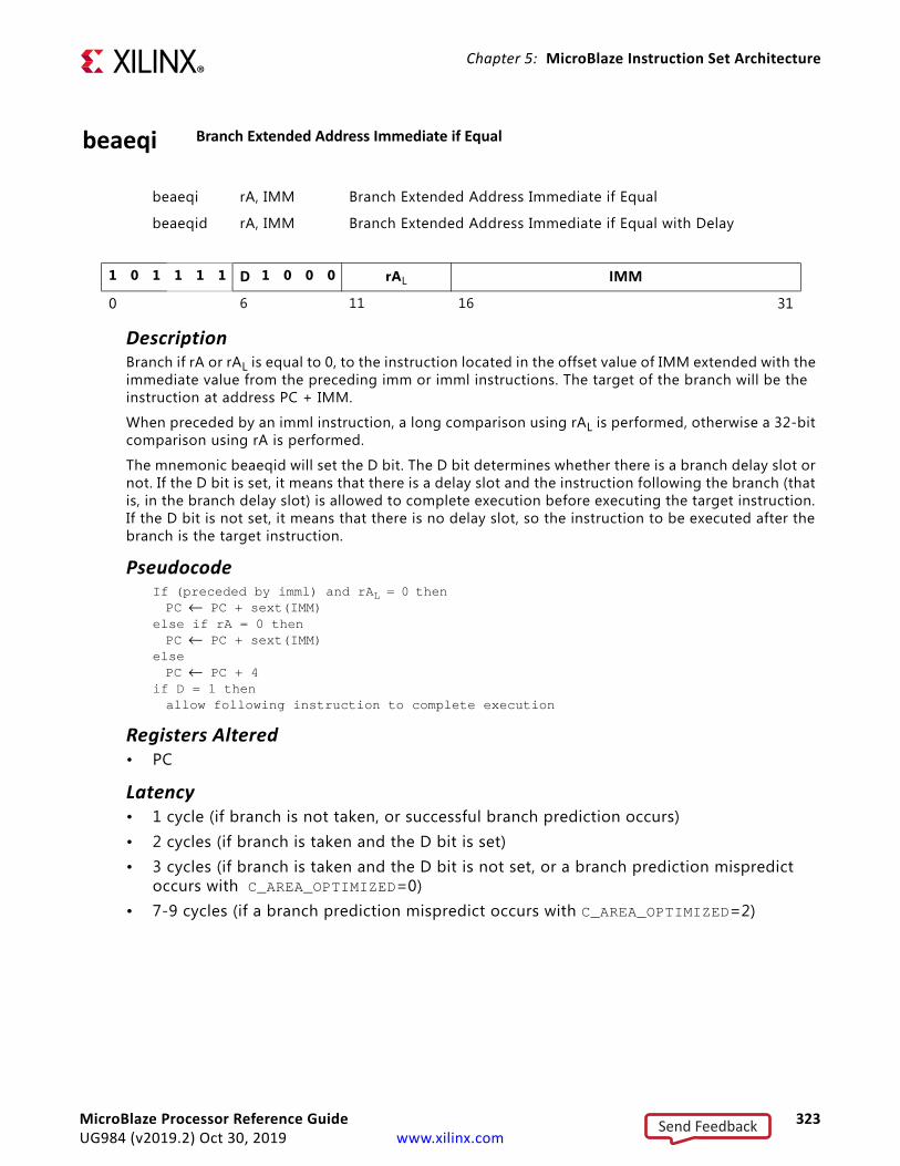
Chapter 5: MicroBlaze Instruction Set Architecture
beaeqi Branch Extended Address Immediate if Equal
beaeqi rA, IMM Branch Extended Address Immediate if Equal
beaeqid rA, IMM Branch Extended Address Immediate if Equal with Delay
1 0 1 1 1 1 D 1 0 0 0 rAL IMM
0 6 11 16 31
DescriptionBranch if rA or rAL is equal to 0, to the instruction located in the offset value of IMM extended with the immediate value from the preceding imm or imml instructions. The target of the branch will be the instruction at address PC + IMM.
When preceded by an imml instruction, a long comparison using rAL is performed, otherwise a 32-bit comparison using rA is performed.
The mnemonic beaeqid will set the D bit. The D bit determines whether there is a branch delay slot or not. If the D bit is set, it means that there is a delay slot and the instruction following the branch (that is, in the branch delay slot) is allowed to complete execution before executing the target instruction. If the D bit is not set, it means that there is no delay slot, so the instruction to be executed after the branch is the target instruction.
PseudocodeIf (preceded by imml) and rAL = 0 then PC ← PC + sext(IMM)
else if rA = 0 thenPC ← PC + sext(IMM)
else PC ← PC + 4
if D = 1 then allow following instruction to complete execution
Registers Altered• PC
Latency• 1 cycle (if branch is not taken, or successful branch prediction occurs)• 2 cycles (if branch is taken and the D bit is set)• 3 cycles (if branch is taken and the D bit is not set, or a branch prediction mispredict
occurs with C_AREA_OPTIMIZED=0)• 7-9 cycles (if a branch prediction mispredict occurs with C_AREA_OPTIMIZED=2)
MicroBlaze Processor Reference Guide 323UG984 (v2019.2) Oct 30, 2019 www.xilinx.com
Send Feedback
Chapter 5: MicroBlaze Instruction Set Architecture
NotesBy default, Type B Branch Long Instructions will take the 16-bit IMM field value and sign extend it to 64 bits to use as the immediate operand. This behavior can be overridden by preceding the Type B instruction with an imm or imml instruction. See the instructions “imm” and “imml” for details on using 64-bit immediate values.
The assembler pseudo-instructions bealeqi and bealeqid are used to indicate a long comparison.
A delay slot must not be used by the following: imm, imml, branch, or break instructions. Interrupts and external hardware breaks are deferred until after the delay slot branch has been completed.
MicroBlaze Processor Reference Guide 324UG984 (v2019.2) Oct 30, 2019 www.xilinx.com
Send Feedback
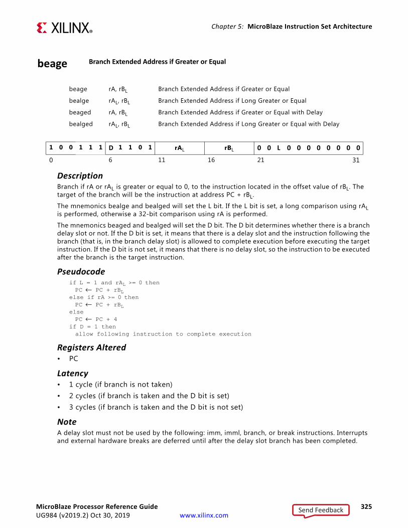
Chapter 5: MicroBlaze Instruction Set Architecture
beage Branch Extended Address if Greater or Equal
beage rA, rBL Branch Extended Address if Greater or Equal
bealge rAL, rBL Branch Extended Address if Long Greater or Equal
beaged rA, rBL Branch Extended Address if Greater or Equal with Delay
bealged rAL, rBL Branch Extended Address if Long Greater or Equal with Delay
1 0 0 1 1 1 D 1 1 0 1 rAL rBL 0 0 L 0 0 0 0 0 0 0 0
0 6 11 16 21 31
DescriptionBranch if rA or rAL is greater or equal to 0, to the instruction located in the offset value of rBL. The target of the branch will be the instruction at address PC + rBL.
The mnemonics bealge and bealged will set the L bit. If the L bit is set, a long comparison using rAL is performed, otherwise a 32-bit comparison using rA is performed.
The mnemonics beaged and bealged will set the D bit. The D bit determines whether there is a branch delay slot or not. If the D bit is set, it means that there is a delay slot and the instruction following the branch (that is, in the branch delay slot) is allowed to complete execution before executing the target instruction. If the D bit is not set, it means that there is no delay slot, so the instruction to be executed after the branch is the target instruction.
Pseudocodeif L = 1 and rAL >= 0 then PC ← PC + rBL
else if rA >= 0 then PC ← PC + rBL
else PC ← PC + 4
if D = 1 then allow following instruction to complete execution
Registers Altered• PC
Latency• 1 cycle (if branch is not taken)• 2 cycles (if branch is taken and the D bit is set)• 3 cycles (if branch is taken and the D bit is not set)
NoteA delay slot must not be used by the following: imm, imml, branch, or break instructions. Interrupts and external hardware breaks are deferred until after the delay slot branch has been completed.
MicroBlaze Processor Reference Guide 325UG984 (v2019.2) Oct 30, 2019 www.xilinx.com
Send Feedback
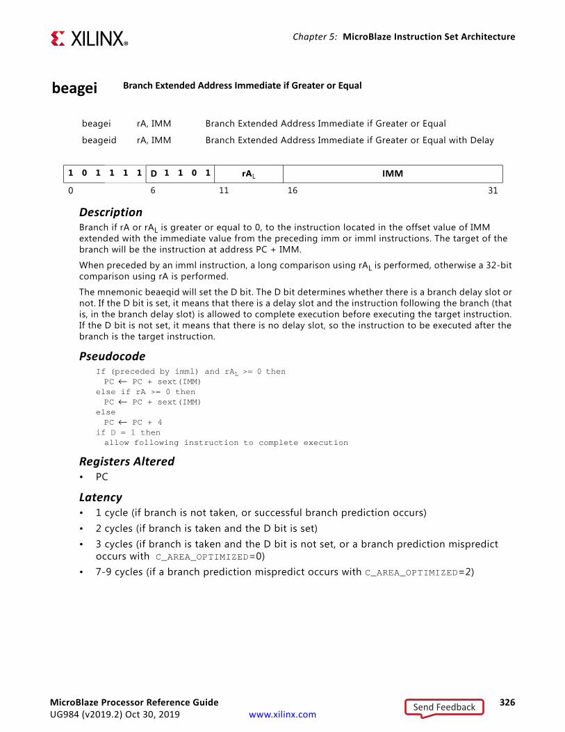
Chapter 5: MicroBlaze Instruction Set Architecture
beagei Branch Extended Address Immediate if Greater or Equal
beagei rA, IMM Branch Extended Address Immediate if Greater or Equal
beageid rA, IMM Branch Extended Address Immediate if Greater or Equal with Delay
1 0 1 1 1 1 D 1 1 0 1 rAL IMM
0 6 11 16 31
DescriptionBranch if rA or rAL is greater or equal to 0, to the instruction located in the offset value of IMM extended with the immediate value from the preceding imm or imml instructions. The target of the branch will be the instruction at address PC + IMM.
When preceded by an imml instruction, a long comparison using rAL is performed, otherwise a 32-bit comparison using rA is performed.
The mnemonic beaeqid will set the D bit. The D bit determines whether there is a branch delay slot or not. If the D bit is set, it means that there is a delay slot and the instruction following the branch (that is, in the branch delay slot) is allowed to complete execution before executing the target instruction. If the D bit is not set, it means that there is no delay slot, so the instruction to be executed after the branch is the target instruction.
PseudocodeIf (preceded by imml) and rAL >= 0 then PC ← PC + sext(IMM)
else if rA >= 0 thenPC ← PC + sext(IMM)
else PC ← PC + 4
if D = 1 then allow following instruction to complete execution
Registers Altered• PC
Latency• 1 cycle (if branch is not taken, or successful branch prediction occurs)• 2 cycles (if branch is taken and the D bit is set)• 3 cycles (if branch is taken and the D bit is not set, or a branch prediction mispredict
occurs with C_AREA_OPTIMIZED=0)• 7-9 cycles (if a branch prediction mispredict occurs with C_AREA_OPTIMIZED=2)
MicroBlaze Processor Reference Guide 326UG984 (v2019.2) Oct 30, 2019 www.xilinx.com
Send Feedback

Chapter 5: MicroBlaze Instruction Set Architecture
NotesBy default, Type B Branch Long Instructions will take the 16-bit IMM field value and sign extend it to 64 bits to use as the immediate operand. This behavior can be overridden by preceding the Type B instruction with an imm or imml instruction. See the instructions “imm” and “imml” for details on using 64-bit immediate values.
The assembler pseudo-instructions bealgei and bealgeid are used to indicate a long comparison.
A delay slot must not be used by the following: imm, imml, branch, or break instructions. Interrupts and external hardware breaks are deferred until after the delay slot branch has been completed.
MicroBlaze Processor Reference Guide 327UG984 (v2019.2) Oct 30, 2019 www.xilinx.com
Send Feedback

Chapter 5: MicroBlaze Instruction Set Architecture
beagt Branch Extended Address if Greater Than
beagt rA, rBL Branch Extended Address if Greater Than
bealgt rAL, rBL Branch Extended Address if Long Greater Than
beagtd rA, rBL Branch Extended Address if Greater Than with Delay
bealgtd rAL, rBL Branch Extended Address if Long Greater Than with Delay
1 0 0 1 1 1 D 1 1 0 0 rAL rBL 0 0 L 0 0 0 0 0 0 0 0
0 6 11 16 21 31
DescriptionBranch if rA or rAL is greater than 0, to the instruction located in the offset value of rBL. The target of the branch will be the instruction at address PC + rBL.
The mnemonics bealgt and bealgtd will set the L bit. If the L bit is set, a long comparison using rAL is performed, otherwise a 32-bit comparison using rA is performed.
The mnemonics beagtd and bealgtd will set the D bit. The D bit determines whether there is a branch delay slot or not. If the D bit is set, it means that there is a delay slot and the instruction following the branch (that is, in the branch delay slot) is allowed to complete execution before executing the target instruction. If the D bit is not set, it means that there is no delay slot, so the instruction to be executed after the branch is the target instruction.
Pseudocodeif L = 1 and rAL > 0 then PC ← PC + rBL
else if rA > 0 then PC ← PC + rBL
else PC ← PC + 4
if D = 1 then allow following instruction to complete execution
Registers Altered• PC
Latency• 1 cycle (if branch is not taken)• 2 cycles (if branch is taken and the D bit is set)• 3 cycles (if branch is taken and the D bit is not set)
NoteA delay slot must not be used by the following: imm, imml, branch, or break instructions. Interrupts and external hardware breaks are deferred until after the delay slot branch has been completed.
MicroBlaze Processor Reference Guide 328UG984 (v2019.2) Oct 30, 2019 www.xilinx.com
Send Feedback
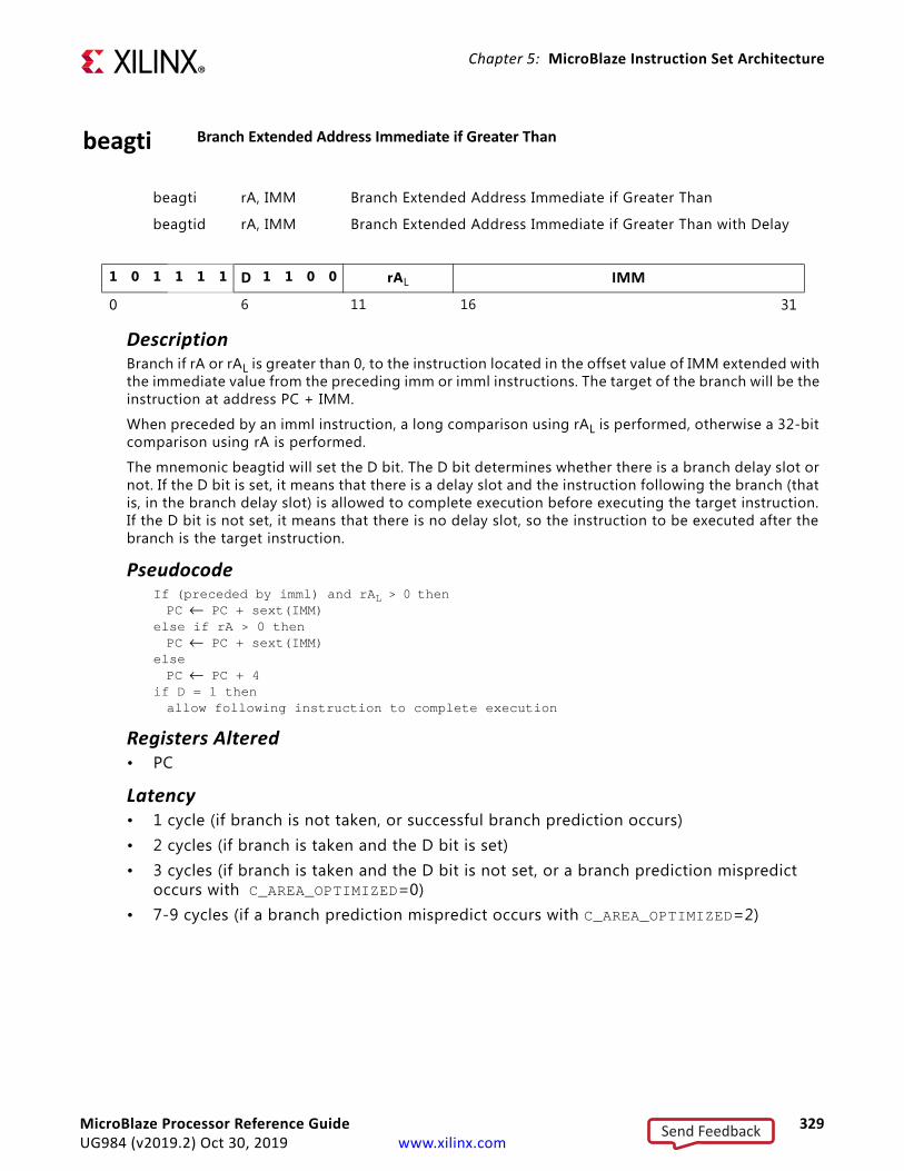
Chapter 5: MicroBlaze Instruction Set Architecture
beagti Branch Extended Address Immediate if Greater Than
beagti rA, IMM Branch Extended Address Immediate if Greater Than
beagtid rA, IMM Branch Extended Address Immediate if Greater Than with Delay
1 0 1 1 1 1 D 1 1 0 0 rAL IMM
0 6 11 16 31
DescriptionBranch if rA or rAL is greater than 0, to the instruction located in the offset value of IMM extended with the immediate value from the preceding imm or imml instructions. The target of the branch will be the instruction at address PC + IMM.
When preceded by an imml instruction, a long comparison using rAL is performed, otherwise a 32-bit comparison using rA is performed.
The mnemonic beagtid will set the D bit. The D bit determines whether there is a branch delay slot or not. If the D bit is set, it means that there is a delay slot and the instruction following the branch (that is, in the branch delay slot) is allowed to complete execution before executing the target instruction. If the D bit is not set, it means that there is no delay slot, so the instruction to be executed after the branch is the target instruction.
PseudocodeIf (preceded by imml) and rAL > 0 then PC ← PC + sext(IMM)
else if rA > 0 thenPC ← PC + sext(IMM)
else PC ← PC + 4
if D = 1 then allow following instruction to complete execution
Registers Altered• PC
Latency• 1 cycle (if branch is not taken, or successful branch prediction occurs)• 2 cycles (if branch is taken and the D bit is set)• 3 cycles (if branch is taken and the D bit is not set, or a branch prediction mispredict
occurs with C_AREA_OPTIMIZED=0)• 7-9 cycles (if a branch prediction mispredict occurs with C_AREA_OPTIMIZED=2)
MicroBlaze Processor Reference Guide 329UG984 (v2019.2) Oct 30, 2019 www.xilinx.com
Send Feedback

Chapter 5: MicroBlaze Instruction Set Architecture
NotesBy default, Type B Branch Long Instructions will take the 16-bit IMM field value and sign extend it to 64 bits to use as the immediate operand. This behavior can be overridden by preceding the Type B instruction with an imm or imml instruction. See the instructions “imm” and “imml” for details on using 64-bit immediate values.
The assembler pseudo-instructions bealgti and bealgtid are used to indicate a long comparison.
A delay slot must not be used by the following: imm, imml, branch, or break instructions. Interrupts and external hardware breaks are deferred until after the delay slot branch has been completed.
MicroBlaze Processor Reference Guide 330UG984 (v2019.2) Oct 30, 2019 www.xilinx.com
Send Feedback
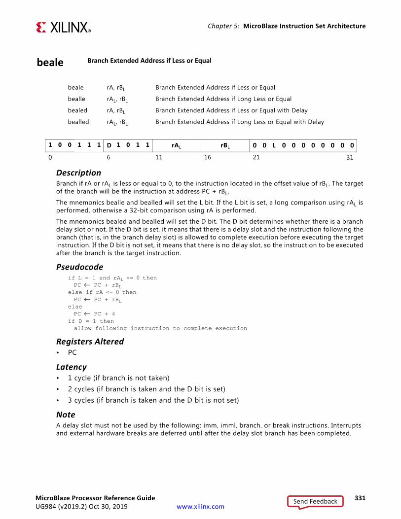
Chapter 5: MicroBlaze Instruction Set Architecture
beale Branch Extended Address if Less or Equal
beale rA, rBL Branch Extended Address if Less or Equal
bealle rAL, rBL Branch Extended Address if Long Less or Equal
bealed rA, rBL Branch Extended Address if Less or Equal with Delay
bealled rAL, rBL Branch Extended Address if Long Less or Equal with Delay
1 0 0 1 1 1 D 1 0 1 1 rAL rBL 0 0 L 0 0 0 0 0 0 0 0
0 6 11 16 21 31
DescriptionBranch if rA or rAL is less or equal to 0, to the instruction located in the offset value of rBL. The target of the branch will be the instruction at address PC + rBL.
The mnemonics bealle and bealled will set the L bit. If the L bit is set, a long comparison using rAL is performed, otherwise a 32-bit comparison using rA is performed.
The mnemonics bealed and bealled will set the D bit. The D bit determines whether there is a branch delay slot or not. If the D bit is set, it means that there is a delay slot and the instruction following the branch (that is, in the branch delay slot) is allowed to complete execution before executing the target instruction. If the D bit is not set, it means that there is no delay slot, so the instruction to be executed after the branch is the target instruction.
Pseudocodeif L = 1 and rAL <= 0 then PC ← PC + rBL
else if rA <= 0 then PC ← PC + rBL
else PC ← PC + 4
if D = 1 then allow following instruction to complete execution
Registers Altered• PC
Latency• 1 cycle (if branch is not taken)• 2 cycles (if branch is taken and the D bit is set)• 3 cycles (if branch is taken and the D bit is not set)
NoteA delay slot must not be used by the following: imm, imml, branch, or break instructions. Interrupts and external hardware breaks are deferred until after the delay slot branch has been completed.
MicroBlaze Processor Reference Guide 331UG984 (v2019.2) Oct 30, 2019 www.xilinx.com
Send Feedback

Chapter 5: MicroBlaze Instruction Set Architecture
bealei Branch Extended Address Immediate if Less or Equal
bealei rA, IMM Branch Extended Address Immediate if Less or Equal
bealeid rA, IMM Branch Extended Address Immediate if Less or Equal with Delay
1 0 1 1 1 1 D 1 0 1 1 rAL IMM
0 6 11 16 31
DescriptionBranch if rA or rAL is less or equal to 0, to the instruction located in the offset value of IMM extended with the immediate value from the preceding imm or imml instructions. The target of the branch will be the instruction at address PC + IMM.
When preceded by an imml instruction, a long comparison using rAL is performed, otherwise a 32-bit comparison using rA is performed.
The mnemonic bealeid will set the D bit. The D bit determines whether there is a branch delay slot or not. If the D bit is set, it means that there is a delay slot and the instruction following the branch (that is, in the branch delay slot) is allowed to complete execution before executing the target instruction. If the D bit is not set, it means that there is no delay slot, so the instruction to be executed after the branch is the target instruction.
PseudocodeIf (preceded by imml) and rAL <= 0 then PC ← PC + sext(IMM)
else if rA <= 0 thenPC ← PC + sext(IMM)
else PC ← PC + 4
if D = 1 then allow following instruction to complete execution
Registers Altered• PC
Latency• 1 cycle (if branch is not taken, or successful branch prediction occurs)• 2 cycles (if branch is taken and the D bit is set)• 3 cycles (if branch is taken and the D bit is not set, or a branch prediction mispredict
occurs with C_AREA_OPTIMIZED=0)• 7-9 cycles (if a branch prediction mispredict occurs with C_AREA_OPTIMIZED=2)
MicroBlaze Processor Reference Guide 332UG984 (v2019.2) Oct 30, 2019 www.xilinx.com
Send Feedback

Chapter 5: MicroBlaze Instruction Set Architecture
NotesBy default, Type B Branch Long Instructions will take the 16-bit IMM field value and sign extend it to 64 bits to use as the immediate operand. This behavior can be overridden by preceding the Type B instruction with an imm or imml instruction. See the instructions “imm” and “imml” for details on using 64-bit immediate values.
The assembler pseudo-instructions beallei and bealleid are used to indicate a long comparison.
A delay slot must not be used by the following: imm, imml, branch, or break instructions. Interrupts and external hardware breaks are deferred until after the delay slot branch has been completed.
MicroBlaze Processor Reference Guide 333UG984 (v2019.2) Oct 30, 2019 www.xilinx.com
Send Feedback

Chapter 5: MicroBlaze Instruction Set Architecture
bealt Branch Extended Address if Less Than
bealt rA, rBL Branch Extended Address if Less Than
beallt rAL, rBL Branch Extended Address if Long Less Than
bealtd rA, rBL Branch Extended Address if Less Than with Delay
bealltd rAL, rBL Branch Extended Address if Long Less Than with Delay
1 0 0 1 1 1 D 1 0 1 0 rAL rBL 0 0 L 0 0 0 0 0 0 0 0
0 6 11 16 21 31
DescriptionBranch if rA or rAL is less than 0, to the instruction located in the offset value of rBL. The target of the branch will be the instruction at address PC + rBL.
The mnemonics beallt and bealltd will set the L bit. If the L bit is set, a long comparison using rAL is performed, otherwise a 32-bit comparison using rA is performed.
The mnemonics bealtd and bealltd will set the D bit. The D bit determines whether there is a branch delay slot or not. If the D bit is set, it means that there is a delay slot and the instruction following the branch (that is, in the branch delay slot) is allowed to complete execution before executing the target instruction. If the D bit is not set, it means that there is no delay slot, so the instruction to be executed after the branch is the target instruction.
Pseudocodeif L = 1 and rAL < 0 then PC ← PC + rBL
else if rA < 0 then PC ← PC + rBL
else PC ← PC + 4
if D = 1 then allow following instruction to complete execution
Registers Altered• PC
Latency• 1 cycle (if branch is not taken)• 2 cycles (if branch is taken and the D bit is set)• 3 cycles (if branch is taken and the D bit is not set)
NoteA delay slot must not be used by the following: imm, imml, branch, or break instructions. Interrupts and external hardware breaks are deferred until after the delay slot branch has been completed.
MicroBlaze Processor Reference Guide 334UG984 (v2019.2) Oct 30, 2019 www.xilinx.com
Send Feedback

Chapter 5: MicroBlaze Instruction Set Architecture
bealti Branch Extended Address Immediate if Less Than
bealti rA, IMM Branch Extended Address Immediate if Less Than
bealtid rA, IMM Branch Extended Address Immediate if Less Than with Delay
1 0 1 1 1 1 D 1 0 1 0 rAL IMM
0 6 11 16 31
DescriptionBranch if rA or rAL is less than 0, to the instruction located in the offset value of IMM extended with the immediate value from the preceding imm or imml instructions. The target of the branch will be the instruction at address PC + IMM.
When preceded by an imml instruction, a long comparison using rAL is performed, otherwise a 32-bit comparison using rA is performed.
The mnemonic bealtid will set the D bit. The D bit determines whether there is a branch delay slot or not. If the D bit is set, it means that there is a delay slot and the instruction following the branch (that is, in the branch delay slot) is allowed to complete execution before executing the target instruction. If the D bit is not set, it means that there is no delay slot, so the instruction to be executed after the branch is the target instruction.
PseudocodeIf (preceded by imml) and rAL < 0 then PC ← PC + sext(IMM)
else if rA < 0 thenPC ← PC + sext(IMM)
else PC ← PC + 4
if D = 1 then allow following instruction to complete execution
Registers Altered• PC
Latency• 1 cycle (if branch is not taken, or successful branch prediction occurs)• 2 cycles (if branch is taken and the D bit is set)• 3 cycles (if branch is taken and the D bit is not set, or a branch prediction mispredict
occurs with C_AREA_OPTIMIZED=0)• 7-9 cycles (if a branch prediction mispredict occurs with C_AREA_OPTIMIZED=2)
MicroBlaze Processor Reference Guide 335UG984 (v2019.2) Oct 30, 2019 www.xilinx.com
Send Feedback

Chapter 5: MicroBlaze Instruction Set Architecture
NotesBy default, Type B Branch Long Instructions will take the 16-bit IMM field value and sign extend it to 64 bits to use as the immediate operand. This behavior can be overridden by preceding the Type B instruction with an imm or imml instruction. See the instructions “imm” and “imml” for details on using 64-bit immediate values.
The assembler pseudo-instructions beallti and bealltid are used to indicate a long comparison.
A delay slot must not be used by the following: imm, imml, branch, or break instructions. Interrupts and external hardware breaks are deferred until after the delay slot branch has been completed.
MicroBlaze Processor Reference Guide 336UG984 (v2019.2) Oct 30, 2019 www.xilinx.com
Send Feedback

Chapter 5: MicroBlaze Instruction Set Architecture
beane Branch Extended Address if Not Equal
beane rA, rBL Branch Extended Address if Not Equal
bealne rAL, rBL Branch Extended Address if Long Not Equal
beaned rA, rBL Branch Extended Address if Not Equal with Delay
bealned rAL, rBL Branch Extended Address if Long Not Equal with Delay
1 0 0 1 1 1 D 1 0 0 1 rAL rBL 0 0 L 0 0 0 0 0 0 0 0
0 6 11 16 21 31
DescriptionBranch if rA or rAL is not equal to 0, to the instruction located in the offset value of rBL. The target of the branch will be the instruction at address PC + rBL.
The mnemonics bealne and bealned will set the L bit. If the L bit is set, a long comparison using rAL is performed, otherwise a 32-bit comparison using rA is performed.
The mnemonics beaned and bealned will set the D bit. The D bit determines whether there is a branch delay slot or not. If the D bit is set, it means that there is a delay slot and the instruction following the branch (that is, in the branch delay slot) is allowed to complete execution before executing the target instruction. If the D bit is not set, it means that there is no delay slot, so the instruction to be executed after the branch is the target instruction.
Pseudocodeif L = 1 and rAL ≠ 0 then PC ← PC + rBL
else if rA ≠ 0 then PC ← PC + rBL
else PC ← PC + 4
if D = 1 then allow following instruction to complete execution
Registers Altered• PC
Latency• 1 cycle (if branch is not taken)• 2 cycles (if branch is taken and the D bit is set)• 3 cycles (if branch is taken and the D bit is not set)
NoteA delay slot must not be used by the following: imm, imml, branch, or break instructions. Interrupts and external hardware breaks are deferred until after the delay slot branch has been completed.
MicroBlaze Processor Reference Guide 337UG984 (v2019.2) Oct 30, 2019 www.xilinx.com
Send Feedback

Chapter 5: MicroBlaze Instruction Set Architecture
beanei Branch Extended Address Immediate if Not Equal
beanei rA, IMM Branch Extended Address Immediate if Not Equal
beaneid rA, IMM Branch Extended Address Immediate if Not Equal with Delay
1 0 1 1 1 1 D 1 0 0 1 rAL IMM
0 6 11 16 31
DescriptionBranch if rA or rAL is not equal to 0, to the instruction located in the offset value of IMM extended with the immediate value from the preceding imm or imml instructions. The target of the branch will be the instruction at address PC + IMM.
When preceded by an imml instruction, a long comparison using rAL is performed, otherwise a 32-bit comparison using rA is performed.
The mnemonic beaneid will set the D bit. The D bit determines whether there is a branch delay slot or not. If the D bit is set, it means that there is a delay slot and the instruction following the branch (that is, in the branch delay slot) is allowed to complete execution before executing the target instruction. If the D bit is not set, it means that there is no delay slot, so the instruction to be executed after the branch is the target instruction.
PseudocodeIf (preceded by imml) and rAL ≠ 0 then PC ← PC + sext(IMM)
else if rA ≠ 0 thenPC ← PC + sext(IMM)
else PC ← PC + 4
if D = 1 then allow following instruction to complete execution
Registers Altered• PC
Latency• 1 cycle (if branch is not taken, or successful branch prediction occurs)• 2 cycles (if branch is taken and the D bit is set)• 3 cycles (if branch is taken and the D bit is not set, or a branch prediction mispredict
occurs with C_AREA_OPTIMIZED=0)• 7-9 cycles (if a branch prediction mispredict occurs with C_AREA_OPTIMIZED=2)
MicroBlaze Processor Reference Guide 338UG984 (v2019.2) Oct 30, 2019 www.xilinx.com
Send Feedback

Chapter 5: MicroBlaze Instruction Set Architecture
NotesBy default, Type B Branch Long Instructions will take the 16-bit IMM field value and sign extend it to 64 bits to use as the immediate operand. This behavior can be overridden by preceding the Type B instruction with an imm or imml instruction. See the instructions “imm” and “imml” for details on using 64-bit immediate values.
The assembler pseudo-instructions bealnei and bealneid are used to indicate a long comparison.
A delay slot must not be used by the following: imm, imml, branch, or break instructions. Interrupts and external hardware breaks are deferred until after the delay slot branch has been completed.
MicroBlaze Processor Reference Guide 339UG984 (v2019.2) Oct 30, 2019 www.xilinx.com
Send Feedback
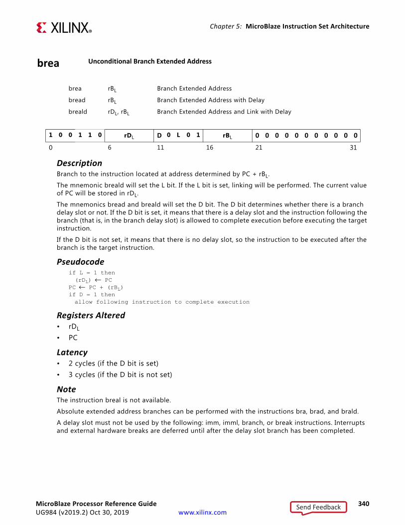
Chapter 5: MicroBlaze Instruction Set Architecture
brea Unconditional Branch Extended Address
brea rBL Branch Extended Address
bread rBL Branch Extended Address with Delay
breald rDL, rBL Branch Extended Address and Link with Delay
1 0 0 1 1 0 rDL D 0 L 0 1 rBL 0 0 0 0 0 0 0 0 0 0 0
0 6 11 16 21 31
DescriptionBranch to the instruction located at address determined by PC + rBL.
The mnemonic breald will set the L bit. If the L bit is set, linking will be performed. The current value of PC will be stored in rDL.
The mnemonics bread and breald will set the D bit. The D bit determines whether there is a branch delay slot or not. If the D bit is set, it means that there is a delay slot and the instruction following the branch (that is, in the branch delay slot) is allowed to complete execution before executing the target instruction.
If the D bit is not set, it means that there is no delay slot, so the instruction to be executed after the branch is the target instruction.
Pseudocodeif L = 1 then (rDL) ← PC
PC ← PC + (rBL)if D = 1 then allow following instruction to complete execution
Registers Altered• rDL • PC
Latency• 2 cycles (if the D bit is set) • 3 cycles (if the D bit is not set)
NoteThe instruction breal is not available.
Absolute extended address branches can be performed with the instructions bra, brad, and brald.
A delay slot must not be used by the following: imm, imml, branch, or break instructions. Interrupts and external hardware breaks are deferred until after the delay slot branch has been completed.
MicroBlaze Processor Reference Guide 340UG984 (v2019.2) Oct 30, 2019 www.xilinx.com
Send Feedback

Chapter 5: MicroBlaze Instruction Set Architecture
breai Unconditional Branch Extended Address Immediate
breai IMM Branch Extended Address Immediate
breaid IMM Branch Extended Address Immediate with Delay
brealid rDL, IMM Branch Extended Address and Link Immediate with Delay
1 0 1 1 1 0 rDL D 0 L 0 1 IMM
0 6 11 16 31
DescriptionBranch to the instruction located at address determined by PC + IMM, extended with the immediate value from the preceding IMM or imml instructions.
The mnemonic brealid will set the L bit. If the L bit is set, linking will be performed. The current value of PC will be stored in rDL.
The mnemonics breaid and brealid will set the D bit. The D bit determines whether there is a branch delay slot or not. If the D bit is set, it means that there is a delay slot and the instruction following the branch (that is, in the branch delay slot) is allowed to complete execution before executing the target instruction. If the D bit is not set, it means that there is no delay slot, so the instruction to be executed after the branch is the target instruction.
Pseudocodeif L = 1 then (rDL) ← PC
PC ← PC + sext(IMM)if D = 1 then allow following instruction to complete execution
Registers Altered• rDL
• PC
Latency• 1 cycle (if successful branch prediction occurs)• 2 cycles (if the D bit is set)• 3 cycles (if the D bit is not set, or a branch prediction mispredict occurs with
C_AREA_OPTIMIZED=0)• 7-9 cycles (if a branch prediction mispredict occurs with C_AREA_OPTIMIZED=2)
MicroBlaze Processor Reference Guide 341UG984 (v2019.2) Oct 30, 2019 www.xilinx.com
Send Feedback

Chapter 5: MicroBlaze Instruction Set Architecture
NotesThe instruction breali is not available.
Absolute extended address branches can be performed with the instructions brai, braid, and bralid.
By default, Type B Branch Long Instructions will take the 16-bit IMM field value and sign extend it to 64 bits to use as the immediate operand. This behavior can be overridden by preceding the Type B instruction with an imm or imml instruction. See the instructions “imm” and “imml” for details on using 64-bit immediate values.
A delay slot must not be used by the following: imm, imml, branch, or break instructions. Interrupts and external hardware breaks are deferred until after the delay slot branch has been completed.
MicroBlaze Processor Reference Guide 342UG984 (v2019.2) Oct 30, 2019 www.xilinx.com
Send Feedback
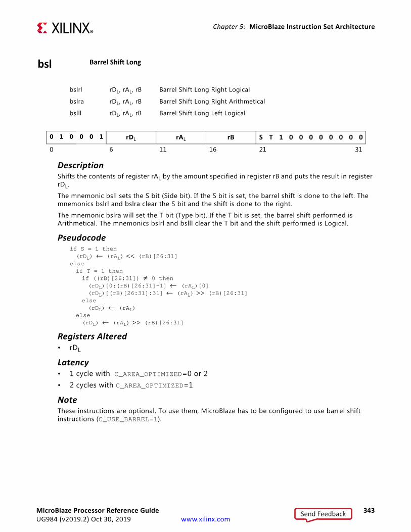
Chapter 5: MicroBlaze Instruction Set Architecture
bsl Barrel Shift Long
bslrl rDL, rAL, rB Barrel Shift Long Right Logical
bslra rDL, rAL, rB Barrel Shift Long Right Arithmetical
bslll rDL, rAL, rB Barrel Shift Long Left Logical
0 1 0 0 0 1 rDL rAL rB S T 1 0 0 0 0 0 0 0 0
0 6 11 16 21 31
DescriptionShifts the contents of register rAL by the amount specified in register rB and puts the result in register rDL.
The mnemonic bsll sets the S bit (Side bit). If the S bit is set, the barrel shift is done to the left. The mnemonics bslrl and bslra clear the S bit and the shift is done to the right.
The mnemonic bslra will set the T bit (Type bit). If the T bit is set, the barrel shift performed is Arithmetical. The mnemonics bslrl and bslll clear the T bit and the shift performed is Logical.
Pseudocodeif S = 1 then(rDL) ← (rAL) << (rB)[26:31]
elseif T = 1 thenif ((rB)[26:31]) ≠ 0 then(rDL)[0:(rB)[26:31]-1] ← (rAL)[0](rDL)[(rB)[26:31]:31] ← (rAL) >> (rB)[26:31]
else(rDL) ← (rAL)
else(rDL) ← (rAL) >> (rB)[26:31]
Registers Altered• rDL
Latency• 1 cycle with C_AREA_OPTIMIZED=0 or 2• 2 cycles with C_AREA_OPTIMIZED=1
NoteThese instructions are optional. To use them, MicroBlaze has to be configured to use barrel shift instructions (C_USE_BARREL=1).
MicroBlaze Processor Reference Guide 343UG984 (v2019.2) Oct 30, 2019 www.xilinx.com
Send Feedback

Chapter 5: MicroBlaze Instruction Set Architecture
bsli Barrel Shift Long Immediate
bslrli rDL, rAL, IMM Barrel Shift Long Right Logical Immediate
bslrai rDL, rAL, IMM Barrel Shift Long Right Arithmetic Immediate
bsllli rDL, rAL, IMM Barrel Shift Long Left Logical Immediate
bslefi rDL, rAL, IMMW, IMMS Barrel Shift Long Extract Field Immediate
bslifi rDL, rAL, Width1, IMMS Barrel Shift Long Insert Field Immediate
1. Width = IMMW - IMMS + 1
0 1 1 0 0 1 rDL rAL 0 0 1 0 0 S T 0 0 0 IMM
0 6 11 16 21 26 31
0 1 1 0 0 1 rDL rAL I E 1 0 IMMW IMMS
0 6 11 16 20 25 26 31
DescriptionThe first three instructions shift the contents of register rAL by the amount specified by IMM and put the result in register rDL.
Barrel Shift Extract Field extracts a bit f ield from register rAL and puts the result in register rDL. The bit f ield width is specif ied by IMMW and the shift amount is specif ied by IMMS. The bit f ield width must be in the range 1 - 63, and the condition IMMW + IMMS ≤ 64 must apply.
Barrel Shift Insert Field inserts a bit field from register rAL into register rDL, modifying the existing value in register rDL. The bit field width is defined by IMMW - IMMS + 1, and the shift amount is specified by IMMS. The condition IMMW ≥ IMMS must apply.
The mnemonic bsllli sets the S bit (Side bit). If the S bit is set, the barrel shift is done to the left. The mnemonics bslrli and bslrai clear the S bit and the shift is done to the right.
The mnemonic bslrai sets the T bit (Type bit). If the T bit is set, the barrel shift performed is Arithmetical. The mnemonics bslrli and bsllli clear the T bit and the shift performed is Logical.
The mnemonic bslefi sets the E bit (Extract bit). In this case the S and T bits are not used.
The mnemonic bslifi sets the I bit (Insert bit). In this case the S and T bits are not used.
MicroBlaze Processor Reference Guide 344UG984 (v2019.2) Oct 30, 2019 www.xilinx.com
Send Feedback
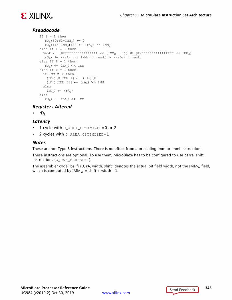
Chapter 5: MicroBlaze Instruction Set Architecture
Pseudocodeif E = 1 then(rDL)[0:63-IMMW] ← 0 (rDL)[64-IMMW:63] ← (rAL) >> IMMS
else if I = 1 thenmask ← (0xffffffffffffffff << (IMMW + 1)) ⊕ (0xffffffffffffffff << IMMS)(rDL) ← ((rAL) << IMMS) ∧ mask) ∨ ((rDL) ∧ mask)
else if S = 1 then(rDL) ← (rAL) << IMM
else if T = 1 thenif IMM ≠ 0 then(rDL)[0:IMM-1] ← (rAL)[0](rDL)[IMM:31] ← (rAL) >> IMM
else(rDL) ← (rAL)
else(rDL) ← (rAL) >> IMM
Registers Altered• rDL
Latency• 1 cycle with C_AREA_OPTIMIZED=0 or 2• 2 cycles with C_AREA_OPTIMIZED=1
NotesThese are not Type B Instructions. There is no effect from a preceding imm or imml instruction.
These instructions are optional. To use them, MicroBlaze has to be configured to use barrel shift instructions (C_USE_BARREL=1).
The assembler code “bslifi rD, rA, width, shift” denotes the actual bit field width, not the IMMW field, which is computed by IMMW = shift + width - 1.
MicroBlaze Processor Reference Guide 345UG984 (v2019.2) Oct 30, 2019 www.xilinx.com
Send Feedback
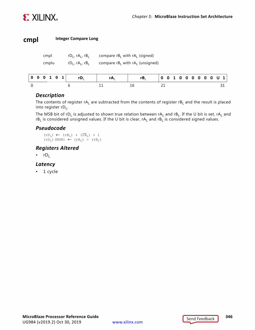
Chapter 5: MicroBlaze Instruction Set Architecture
cmpl Integer Compare Long
cmpl rDL, rAL, rBL compare rBL with rAL (signed)
cmplu rDL, rAL, rBL compare rBL with rAL (unsigned)
0 0 0 1 0 1 rDL rAL rBL 0 0 1 0 0 0 0 0 0 U 1
0 6 11 16 21 31
DescriptionThe contents of register rAL are subtracted from the contents of register rBL and the result is placed into register rDL.
The MSB bit of rDL is adjusted to shown true relation between rAL and rBL. If the U bit is set, rAL and rBL is considered unsigned values. If the U bit is clear, rAL and rBL is considered signed values.
Pseudocode(rDL) ← (rBL) + (rAL) + 1(rDL)(MSB) ← (rAL) > (rBL)
Registers Altered• rDL
Latency• 1 cycle
MicroBlaze Processor Reference Guide 346UG984 (v2019.2) Oct 30, 2019 www.xilinx.com
Send Feedback
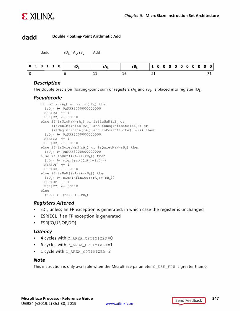
Chapter 5: MicroBlaze Instruction Set Architecture
dadd Double Floating-Point Arithmetic Add
dadd rDL, rAL, rBL Add
0 1 0 1 1 0 rDL rAL rBL 1 0 0 0 0 0 0 0 0 0 0
0 6 11 16 21 31
DescriptionThe double precision floating-point sum of registers rAL and rBL, is placed into register rDL.
Pseudocodeif isDnz(rAL) or isDnz(rBL) then(rDL) ← 0xFFF8000000000000FSR[DO] ← 1ESR[EC] ← 00110
else if isSigNaN(rAL) or isSigNaN(rBL)or (isPosInfinite(rAL) and isNegInfinite(rBL)) or(isNegInfinite(rAL) and isPosInfinite(rBL))) then
(rDL) ← 0xFFF8000000000000FSR[IO] ← 1ESR[EC] ← 00110
else if isQuietNaN(rAL) or isQuietNaN(rBL) then(rDL) ← 0xFFF8000000000000
else if isDnz((rAL)+(rBL)) then(rDL) ← signZero((rAL)+(rBL))FSR[UF] ← 1ESR[EC] ← 00110
else if isNaN((rAL)+(rBL)) then(rDL) ← signInfinite((rAL)+(rBL))FSR[OF] ← 1ESR[EC] ← 00110
else(rDL) ← (rAL) + (rBL)
Registers Altered• rDL, unless an FP exception is generated, in which case the register is unchanged• ESR[EC], if an FP exception is generated• FSR[IO,UF,OF,DO]
Latency• 4 cycles with C_AREA_OPTIMIZED=0• 6 cycles with C_AREA_OPTIMIZED=1• 1 cycle with C_AREA_OPTIMIZED=2
NoteThis instruction is only available when the MicroBlaze parameter C_USE_FPU is greater than 0.
MicroBlaze Processor Reference Guide 347UG984 (v2019.2) Oct 30, 2019 www.xilinx.com
Send Feedback
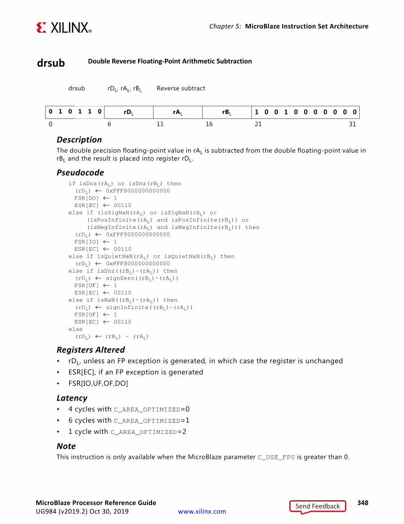
Chapter 5: MicroBlaze Instruction Set Architecture
drsub Double Reverse Floating-Point Arithmetic Subtraction
drsub rDL, rAL, rBL Reverse subtract
0 1 0 1 1 0 rDL rAL rBL 1 0 0 1 0 0 0 0 0 0 0
0 6 11 16 21 31
DescriptionThe double precision floating-point value in rAL is subtracted from the double floating-point value in rBL and the result is placed into register rDL.
Pseudocodeif isDnz(rAL) or isDnz(rBL) then(rDL) ← 0xFFF8000000000000FSR[DO] ← 1ESR[EC] ← 00110
else if (isSigNaN(rAL) or isSigNaN(rBL) or (isPosInfinite(rAL) and isPosInfinite(rBL)) or(isNegInfinite(rAL) and isNegInfinite(rBL))) then
(rDL) ← 0xFFF8000000000000FSR[IO] ← 1ESR[EC] ← 00110
else if isQuietNaN(rAL) or isQuietNaN(rBL) then(rDL) ← 0xFFF8000000000000
else if isDnz((rBL)-(rAL)) then(rDL) ← signZero((rBL)-(rAL))FSR[UF] ← 1ESR[EC] ← 00110
else if isNaN((rBL)-(rAL)) then(rDL) ← signInfinite((rBL)-(rAL))FSR[OF] ← 1ESR[EC] ← 00110
else(rDL) ← (rBL) - (rAL)
Registers Altered• rDL, unless an FP exception is generated, in which case the register is unchanged• ESR[EC], if an FP exception is generated• FSR[IO,UF,OF,DO]
Latency• 4 cycles with C_AREA_OPTIMIZED=0• 6 cycles with C_AREA_OPTIMIZED=1• 1 cycle with C_AREA_OPTIMIZED=2
NoteThis instruction is only available when the MicroBlaze parameter C_USE_FPU is greater than 0.
MicroBlaze Processor Reference Guide 348UG984 (v2019.2) Oct 30, 2019 www.xilinx.com
Send Feedback

Chapter 5: MicroBlaze Instruction Set Architecture
dmul Double Floating-Point Arithmetic Multiplication
dmul rDL, rAL, rBL Multiply
0 1 0 1 1 0 rDL rAL rBL 1 0 1 0 0 0 0 0 0 0 0
0 6 11 16 21 31
DescriptionThe double precision floating-point value in rAL is multiplied with the double floating-point value in rBL and the result is placed into register rDL.
Pseudocodeif isDnz(rAL) or isDnz(rBL) then(rDL) ← 0xFFF8000000000000FSR[DO] ← 1ESR[EC] ← 00110
else if isSigNaN(rAL) or isSigNaN(rBL) or (isZero(rAL) and isInfinite(rBL)) or
(isZero(rBL) and isInfinite(rAL)) then(rDL) ← 0xFFF8000000000000FSR[IO] ← 1ESR[EC] ← 00110
else if isQuietNaN(rAL) or isQuietNaN(rBL) then(rDL) ← 0xFFF8000000000000
else if isDnz((rBL)*(rAL)) then(rDL) ← signZero((rAL)*(rBL))FSR[UF] ← 1ESR[EC] ← 00110
else if isNaN((rBL)*(rAL)) then(rDL) ← signInfinite((rBL)*(rAL))FSR[OF] ← 1ESR[EC] ← 00110
else(rDL) ← (rBL) * (rAL)
Registers Altered• rDL, unless an FP exception is generated, in which case the register is unchanged• ESR[EC], if an FP exception is generated• FSR[IO,UF,OF,DO]
Latency• 4 cycles with C_AREA_OPTIMIZED=0• 6 cycles with C_AREA_OPTIMIZED=1• 1 cycle with C_AREA_OPTIMIZED=2
NoteThis instruction is only available when the MicroBlaze parameter C_USE_FPU is greater than 0.
MicroBlaze Processor Reference Guide 349UG984 (v2019.2) Oct 30, 2019 www.xilinx.com
Send Feedback

Chapter 5: MicroBlaze Instruction Set Architecture
ddiv Double Floating-Point Arithmetic Division
ddiv rDL, rAL, rBL Divide
0 1 0 1 1 0 rDL rAL rBL 1 0 1 1 0 0 0 0 0 0 0
0 6 11 16 21 31
DescriptionThe double precision floating-point value in rBL is divided by the double floating-point value in rAL and the result is placed into register rDL.
Pseudocodeif isDnz(rAL) or isDnz(rBL) then(rDL) ← 0xFFF8000000000000FSR[DO] ← 1ESR[EC] ← 00110
else if isSigNaN(rAL) or isSigNaN(rBL) or (isZero(rAL) and isZero(rBL)) or
(isInfinite(rAL) and isInfinite(rBL)) then(rDL) ← 0xFFF8000000000000FSR[IO] ← 1ESR[EC] ← 00110
else if isQuietNaN(rAL) or isQuietNaN(rBL) then(rDL) ← 0xFFF8000000000000
else if isZero(rAL) and not isInfinite(rBL) then(rDL) ← signInfinite((rBL)/(rAL))FSR[DZ] ← 1ESR[EC] ← 00110
else if isDnz((rBL) / (rAL)) then(rDL) ← signZero((rBL) / (rAL))FSR[UF] ← 1ESR[EC] ← 00110
else if isNaN((rBL)/(rAL)) then(rDL) ← signInfinite((rBL) / (rAL))FSR[OF] ← 1ESR[EC] ← 00110
else(rDL) ← (rBL) / (rAL)
Registers Altered• rDL, unless an FP exception is generated, in which case the register is unchanged• ESR[EC], if an FP exception is generated• FSR[IO,UF,OF,DO,DZ]
Latency• 28 cycles with C_AREA_OPTIMIZED=0• 30 cycles with C_AREA_OPTIMIZED=1• 24 cycles with C_AREA_OPTIMIZED=2
NoteThis instruction is only available when the MicroBlaze parameter C_USE_FPU is greater than 0.
MicroBlaze Processor Reference Guide 350UG984 (v2019.2) Oct 30, 2019 www.xilinx.com
Send Feedback
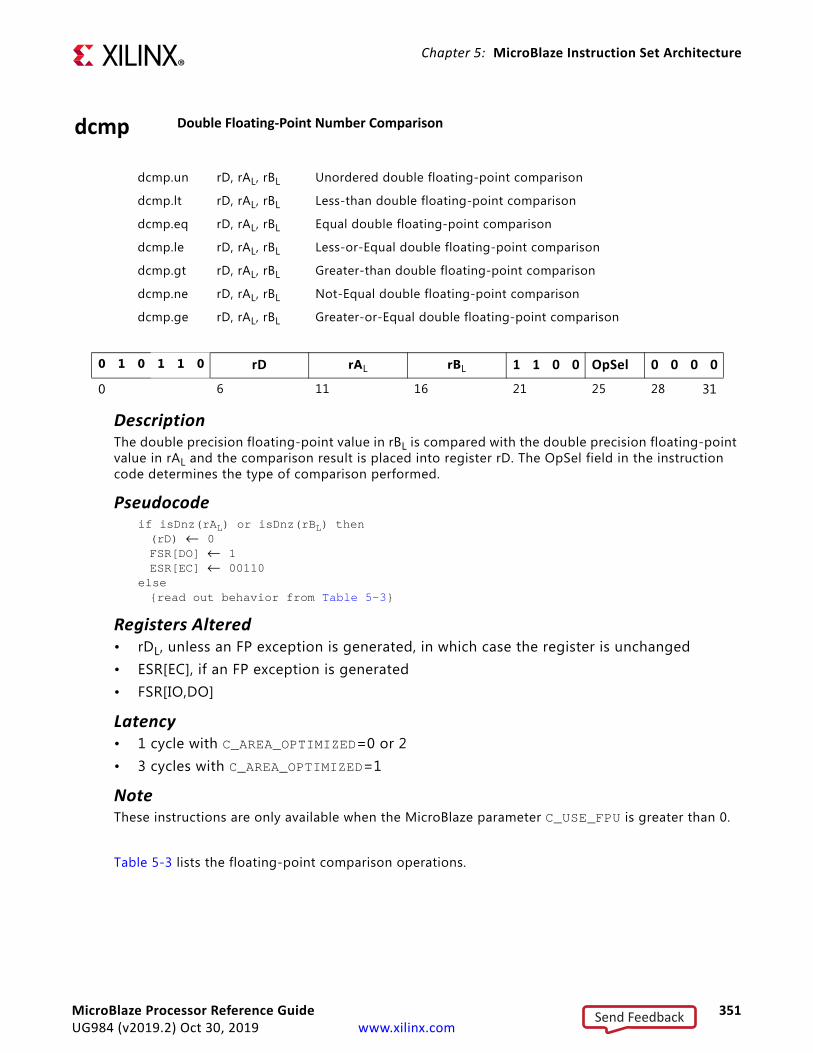
Chapter 5: MicroBlaze Instruction Set Architecture
dcmp Double Floating-Point Number Comparison
dcmp.un rD, rAL, rBL Unordered double floating-point comparison
dcmp.lt rD, rAL, rBL Less-than double floating-point comparison
dcmp.eq rD, rAL, rBL Equal double floating-point comparison
dcmp.le rD, rAL, rBL Less-or-Equal double floating-point comparison
dcmp.gt rD, rAL, rBL Greater-than double floating-point comparison
dcmp.ne rD, rAL, rBL Not-Equal double floating-point comparison
dcmp.ge rD, rAL, rBL Greater-or-Equal double floating-point comparison
0 1 0 1 1 0 rD rAL rBL 1 1 0 0 OpSel 0 0 0 0
0 6 11 16 21 25 28 31
DescriptionThe double precision floating-point value in rBL is compared with the double precision floating-point value in rAL and the comparison result is placed into register rD. The OpSel field in the instruction code determines the type of comparison performed.
Pseudocodeif isDnz(rAL) or isDnz(rBL) then(rD) ← 0FSR[DO] ← 1ESR[EC] ← 00110
else{read out behavior from Table 5-3}
Registers Altered• rDL, unless an FP exception is generated, in which case the register is unchanged• ESR[EC], if an FP exception is generated• FSR[IO,DO]
Latency• 1 cycle with C_AREA_OPTIMIZED=0 or 2• 3 cycles with C_AREA_OPTIMIZED=1
NoteThese instructions are only available when the MicroBlaze parameter C_USE_FPU is greater than 0.
Table 5-3 lists the floating-point comparison operations.
MicroBlaze Processor Reference Guide 351UG984 (v2019.2) Oct 30, 2019 www.xilinx.com
Send Feedback
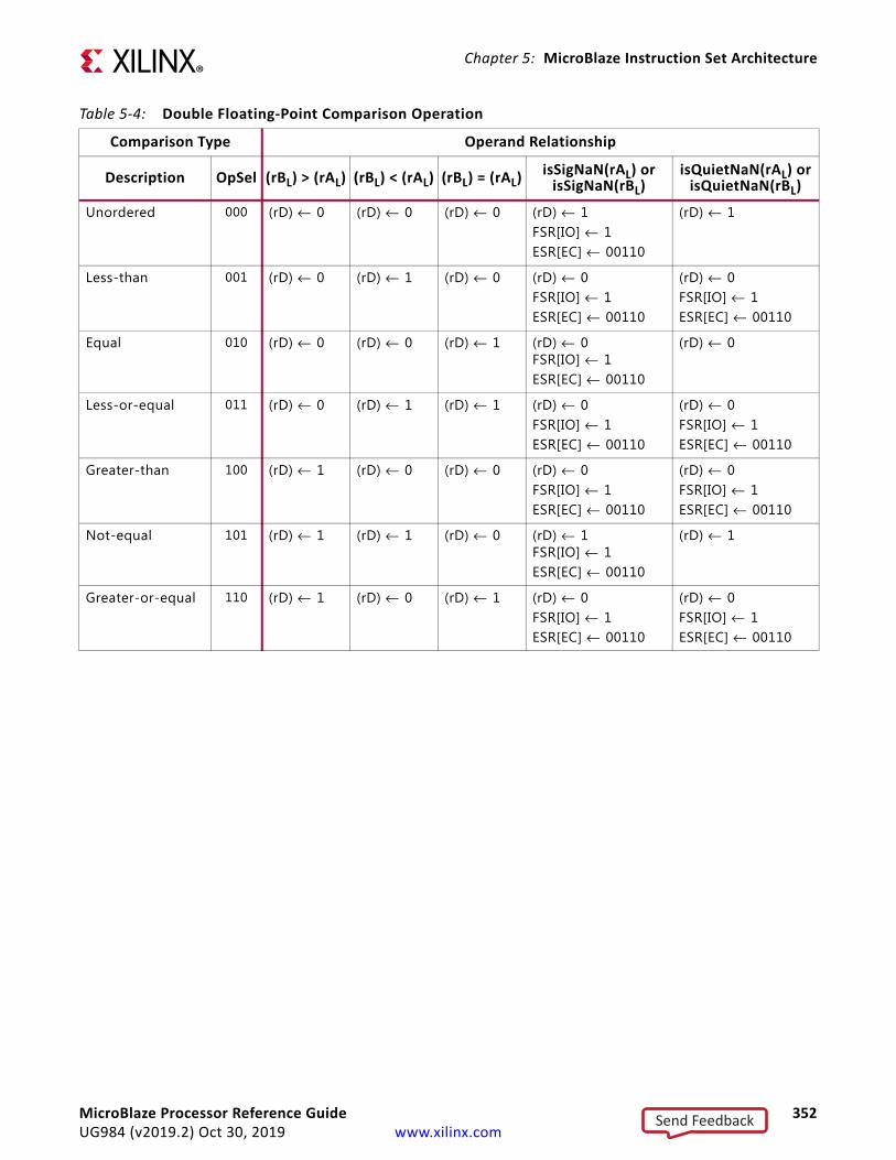
Chapter 5: MicroBlaze Instruction Set Architecture
Table 5-4: Double Floating-Point Comparison Operation
Comparison Type Operand Relationship
Description OpSel (rBL) > (rAL) (rBL) < (rAL) (rBL) = (rAL) isSigNaN(rAL) or isSigNaN(rBL)
isQuietNaN(rAL) or isQuietNaN(rBL)
Unordered 000 (rD) ← 0 (rD) ← 0 (rD) ← 0 (rD) ← 1FSR[IO] ← 1ESR[EC] ← 00110
(rD) ← 1
Less-than 001 (rD) ← 0 (rD) ← 1 (rD) ← 0 (rD) ← 0FSR[IO] ← 1ESR[EC] ← 00110
(rD) ← 0FSR[IO] ← 1ESR[EC] ← 00110
Equal 010 (rD) ← 0 (rD) ← 0 (rD) ← 1 (rD) ← 0 FSR[IO] ← 1ESR[EC] ← 00110
(rD) ← 0
Less-or-equal 011 (rD) ← 0 (rD) ← 1 (rD) ← 1 (rD) ← 0FSR[IO] ← 1ESR[EC] ← 00110
(rD) ← 0FSR[IO] ← 1ESR[EC] ← 00110
Greater-than 100 (rD) ← 1 (rD) ← 0 (rD) ← 0 (rD) ← 0FSR[IO] ← 1ESR[EC] ← 00110
(rD) ← 0FSR[IO] ← 1ESR[EC] ← 00110
Not-equal 101 (rD) ← 1 (rD) ← 1 (rD) ← 0 (rD) ← 1 FSR[IO] ← 1ESR[EC] ← 00110
(rD) ← 1
Greater-or-equal 110 (rD) ← 1 (rD) ← 0 (rD) ← 1 (rD) ← 0FSR[IO] ← 1ESR[EC] ← 00110
(rD) ← 0FSR[IO] ← 1ESR[EC] ← 00110
MicroBlaze Processor Reference Guide 352UG984 (v2019.2) Oct 30, 2019 www.xilinx.com
Send Feedback
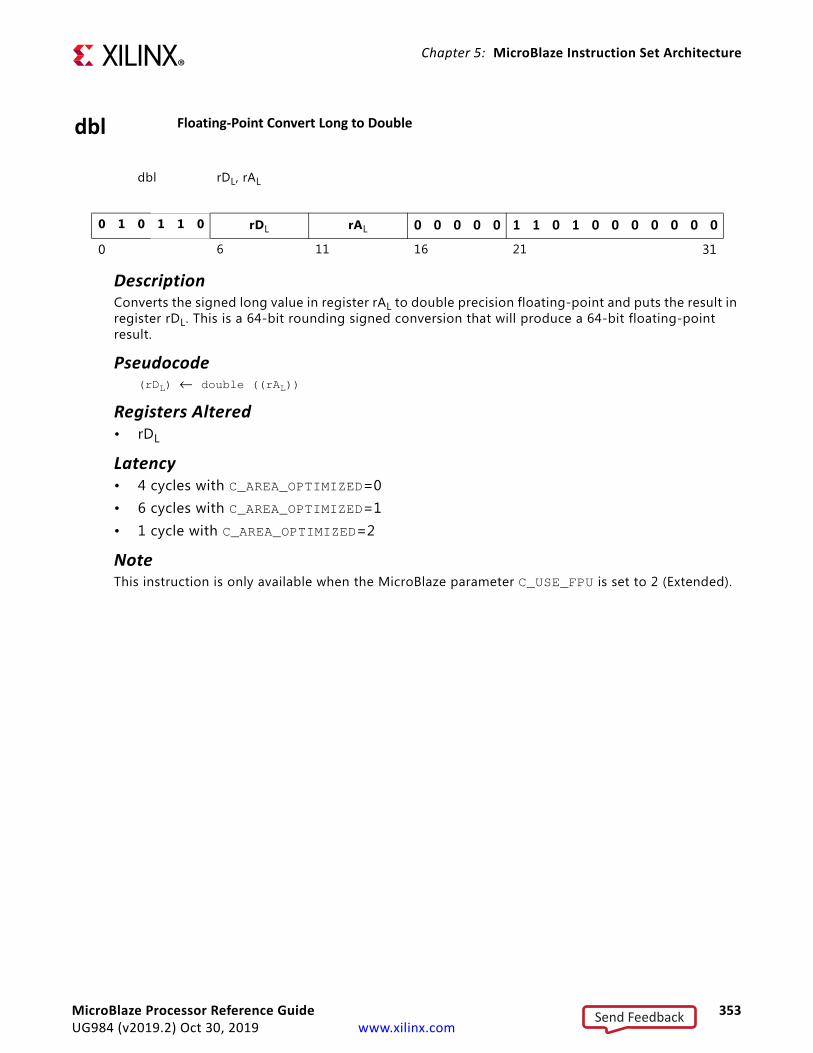
Chapter 5: MicroBlaze Instruction Set Architecture
dbl Floating-Point Convert Long to Double
dbl rDL, rAL
0 1 0 1 1 0 rDL rAL 0 0 0 0 0 1 1 0 1 0 0 0 0 0 0 0
0 6 11 16 21 31
DescriptionConverts the signed long value in register rAL to double precision floating-point and puts the result in register rDL. This is a 64-bit rounding signed conversion that will produce a 64-bit floating-point result.
Pseudocode(rDL) ← double ((rAL))
Registers Altered• rDL
Latency• 4 cycles with C_AREA_OPTIMIZED=0• 6 cycles with C_AREA_OPTIMIZED=1• 1 cycle with C_AREA_OPTIMIZED=2
NoteThis instruction is only available when the MicroBlaze parameter C_USE_FPU is set to 2 (Extended).
MicroBlaze Processor Reference Guide 353UG984 (v2019.2) Oct 30, 2019 www.xilinx.com
Send Feedback

Chapter 5: MicroBlaze Instruction Set Architecture
dlong Floating-Point Convert Double to Long
dlong rDL, rAL
0 1 0 1 1 0 rDL rAL 0 0 0 0 0 1 1 1 0 0 0 0 0 0 0 0
0 6 11 16 21 31
DescriptionConverts the double precision floating-point number in register rAL to a signed long value and puts the result in register rDL. This is a 64-bit signed conversion that will produce a 64-bit long result.
Pseudocodeif isDnz(rAL) then(rDL) ← 0xFFF8000000000000FSR[DO] ← 1ESR[EC] ← 00110
else if isNaN(rAL) then(rDL) ← 0xFFF8000000000000FSR[IO] ← 1ESR[EC] ← 00110
else if isInf(rAL) or (rAL) < -263 or (rAL) > 2
63 - 1 then(rDL) ← 0xFFF8000000000000FSR[IO] ← 1ESR[EC] ← 00110
else(rDL) ← long ((rAL))
Registers Altered• rDL, unless an FP exception is generated, in which case the register is unchanged• ESR[EC], if an FP exception is generated• FSR[IO,DO]
Latency• 5 cycles with C_AREA_OPTIMIZED=0• 7 cycles with C_AREA_OPTIMIZED=1• 2 cycles with C_AREA_OPTIMIZED=2
NoteThis instruction is only available when the MicroBlaze parameter C_USE_FPU is set to 2 (Extended).
MicroBlaze Processor Reference Guide 354UG984 (v2019.2) Oct 30, 2019 www.xilinx.com
Send Feedback
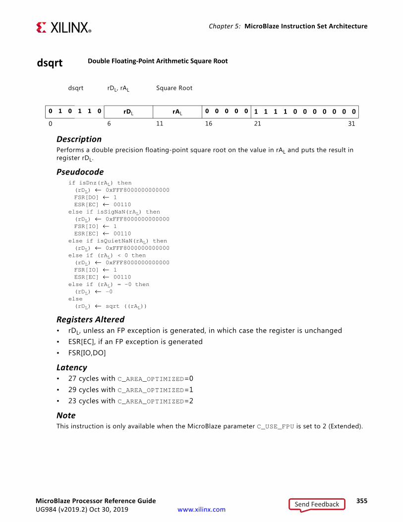
Chapter 5: MicroBlaze Instruction Set Architecture
dsqrt Double Floating-Point Arithmetic Square Root
dsqrt rDL, rAL Square Root
0 1 0 1 1 0 rDL rAL 0 0 0 0 0 1 1 1 1 0 0 0 0 0 0 0
0 6 11 16 21 31
DescriptionPerforms a double precision floating-point square root on the value in rAL and puts the result in register rDL.
Pseudocodeif isDnz(rAL) then(rDL) ← 0xFFF8000000000000FSR[DO] ← 1ESR[EC] ← 00110
else if isSigNaN(rAL) then(rDL) ← 0xFFF8000000000000FSR[IO] ← 1ESR[EC] ← 00110
else if isQuietNaN(rAL) then(rDL) ← 0xFFF8000000000000
else if (rAL) < 0 then(rDL) ← 0xFFF8000000000000FSR[IO] ← 1ESR[EC] ← 00110
else if (rAL) = -0 then(rDL) ← -0
else(rDL) ← sqrt ((rAL))
Registers Altered• rDL, unless an FP exception is generated, in which case the register is unchanged• ESR[EC], if an FP exception is generated• FSR[IO,DO]
Latency• 27 cycles with C_AREA_OPTIMIZED=0• 29 cycles with C_AREA_OPTIMIZED=1• 23 cycles with C_AREA_OPTIMIZED=2
NoteThis instruction is only available when the MicroBlaze parameter C_USE_FPU is set to 2 (Extended).
MicroBlaze Processor Reference Guide 355UG984 (v2019.2) Oct 30, 2019 www.xilinx.com
Send Feedback
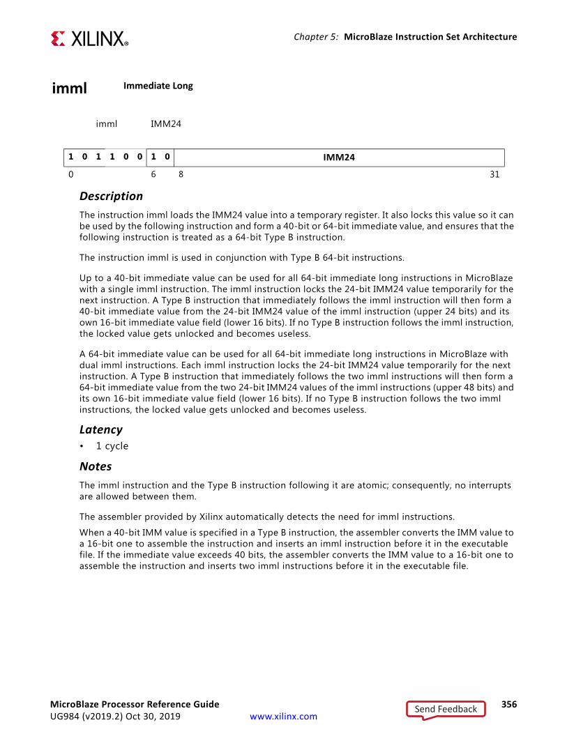
Chapter 5: MicroBlaze Instruction Set Architecture
imml Immediate Long
imml IMM24
1 0 1 1 0 0 1 0 IMM24
0 6 8 31
DescriptionThe instruction imml loads the IMM24 value into a temporary register. It also locks this value so it can be used by the following instruction and form a 40-bit or 64-bit immediate value, and ensures that the following instruction is treated as a 64-bit Type B instruction.
The instruction imml is used in conjunction with Type B 64-bit instructions.
Up to a 40-bit immediate value can be used for all 64-bit immediate long instructions in MicroBlaze with a single imml instruction. The imml instruction locks the 24-bit IMM24 value temporarily for the next instruction. A Type B instruction that immediately follows the imml instruction will then form a 40-bit immediate value from the 24-bit IMM24 value of the imml instruction (upper 24 bits) and its own 16-bit immediate value field (lower 16 bits). If no Type B instruction follows the imml instruction, the locked value gets unlocked and becomes useless.
A 64-bit immediate value can be used for all 64-bit immediate long instructions in MicroBlaze with dual imml instructions. Each imml instruction locks the 24-bit IMM24 value temporarily for the next instruction. A Type B instruction that immediately follows the two imml instructions will then form a 64-bit immediate value from the two 24-bit IMM24 values of the imml instructions (upper 48 bits) and its own 16-bit immediate value field (lower 16 bits). If no Type B instruction follows the two imml instructions, the locked value gets unlocked and becomes useless.
Latency• 1 cycle
NotesThe imml instruction and the Type B instruction following it are atomic; consequently, no interrupts are allowed between them.
The assembler provided by Xilinx automatically detects the need for imml instructions.
When a 40-bit IMM value is specified in a Type B instruction, the assembler converts the IMM value to a 16-bit one to assemble the instruction and inserts an imml instruction before it in the executable file. If the immediate value exceeds 40 bits, the assembler converts the IMM value to a 16-bit one to assemble the instruction and inserts two imml instructions before it in the executable file.
MicroBlaze Processor Reference Guide 356UG984 (v2019.2) Oct 30, 2019 www.xilinx.com
Send Feedback

Chapter 5: MicroBlaze Instruction Set Architecture
ll Load Long
ll rDL, rAL, rBL
llr rDL, rAL, rBL
1 1 0 0 1 0 rDL rAL rBL 0 R 1 0 0 0 0 0 0 0 0
0 6 11 16 21 31
DescriptionLoads a long (64 bits) from the long aligned memory location that results from adding the contents of registers rAL and rBL. The data is placed in register rDL.
If the R bit is set, the bytes in the loaded word are reversed , loading data with the opposite endianness of the endianness defined by the E bit (if virtual protected mode is enabled).
A data TLB miss exception occurs if virtual protected mode is enabled, and a valid translation entry corresponding to the address is not found in the TLB.
A data storage exception occurs if access is prevented by a no-access-allowed zone protection. This only applies to accesses with user mode and virtual protected mode enabled.
An unaligned data access exception occurs if the three least significant bits in the address are not zero.
PseudocodeAddr ← (rAL) + (rBL) if TLB_Miss(Addr) and MSR[VM] = 1 thenESR[EC]← 10010;ESR[S]← 0MSR[UMS] ← MSR[UM]; MSR[VMS] ← MSR[VM]; MSR[UM] ← 0; MSR[VM] ← 0
else if Access_Protected(Addr) and MSR[UM] = 1 and MSR[VM] = 1 thenESR[EC] ← 10000;ESR[S]← 0; ESR[DIZ] ← 1MSR[UMS]← MSR[UM]; MSR[VMS] ← MSR[VM]; MSR[UM] ← 0; MSR[VM] ← 0
else if Addr[C_ADDR_SIZE-3:C_ADDR_SIZE-1] ≠ 0 thenESR[EC] ← 00001; ESR[W] ← 1; ESR[S] ← 0; ESR[Rx] ← rD
else (rDL) ← Mem(Addr)
Registers Altered• rDL, unless an exception is generated, in which case the register is unchanged• MSR[UM], MSR[VM], MSR[UMS], MSR[VMS], if a TLB miss exception or a data storage
exception is generated• ESR[EC], ESR[S], if an exception is generated• ESR[DIZ], if a data storage exception is generated• ESR[W], ESR[Rx], if an unaligned data access exception is generated
Latency• 2 cycles with C_AREA_OPTIMIZED=0 or 2• 3 cycles with C_AREA_OPTIMIZED=1
MicroBlaze Processor Reference Guide 357UG984 (v2019.2) Oct 30, 2019 www.xilinx.com
Send Feedback

Chapter 5: MicroBlaze Instruction Set Architecture
NotesThe long reversed instruction is only valid if MicroBlaze is configured to use reorder instructions (C_USE_REORDER_INSTR = 1).
MicroBlaze Processor Reference Guide 358UG984 (v2019.2) Oct 30, 2019 www.xilinx.com
Send Feedback

Chapter 5: MicroBlaze Instruction Set Architecture
lli Load Long Immediate
lli rDL, rAL, IMM
1 1 1 0 1 1 rDL rAL IMM
0 6 11 16 31
DescriptionLoads a long (64 bits) from the long aligned memory location that results from adding the contents of register rAL and the sign-extended IMM value. The data is placed in register rDL.
A data TLB miss exception occurs if virtual protected mode is enabled, and a valid translation entry corresponding to the address is not found in the TLB.
A data storage exception occurs if access is prevented by a no-access-allowed zone protection. This only applies to accesses with user mode and virtual protected mode enabled.
An unaligned data access exception occurs if the three least significant bits in the address are not zero
PseudocodeAddr ← (rAL) + sext(IMM) if TLB_Miss(Addr) and MSR[VM] = 1 thenESR[EC]← 10010;ESR[S]← 0MSR[UMS] ← MSR[UM]; MSR[VMS] ← MSR[VM]; MSR[UM] ← 0; MSR[VM] ← 0
else if Access_Protected(Addr) and MSR[UM] = 1 and MSR[VM] = 1 thenESR[EC] ← 10000;ESR[S]← 0; ESR[DIZ] ← 1MSR[UMS]← MSR[UM]; MSR[VMS] ← MSR[VM]; MSR[UM] ← 0; MSR[VM] ← 0
else if Addr[C_ADDR_SIZE-3:C_ADDR_SIZE-1] ≠ 0 thenESR[EC] ← 00001; ESR[W] ← 1; ESR[S] ← 0; ESR[Rx] ← rD
else (rDL) ← Mem(Addr)
Registers Altered• rDL, unless an exception is generated, in which case the register is unchanged• MSR[UM], MSR[VM], MSR[UMS], MSR[VMS], if a TLB miss exception or a data storage
exception is generated• ESR[EC], ESR[S], if an exception is generated• ESR[DIZ], if a data storage exception is generated• ESR[W], ESR[Rx], if an unaligned data access exception is generated
Latency• 2 cycles with C_AREA_OPTIMIZED=0 or 2• 3 cycles with C_AREA_OPTIMIZED=1
NoteBy default, Type B load immediate instructions will take the 16-bit IMM field value and sign extend it to 64 bits to use as the immediate operand. This behavior can be overridden by preceding the Type B instruction with an imm or imml instruction. See the instructions “imm” and “imml” for details on using 64-bit immediate values.
MicroBlaze Processor Reference Guide 359UG984 (v2019.2) Oct 30, 2019 www.xilinx.com
Send Feedback

Chapter 5: MicroBlaze Instruction Set Architecture
orl Logical OR Long
orl rDL, rAL, rBL
1 0 0 0 0 0 rDL rAL rBL 0 0 1 0 0 0 0 0 0 0 0
0 6 11 16 21 31
DescriptionThe contents of register rAL are ORed with the contents of register rBL; the result is placed into register rDL.
Pseudocode(rDL) ← (rAL) ∨ (rBL)
Registers Altered• rDL
Latency• 1 cycle
MicroBlaze Processor Reference Guide 360UG984 (v2019.2) Oct 30, 2019 www.xilinx.com
Send Feedback

Chapter 5: MicroBlaze Instruction Set Architecture
orli Logical OR Long with Immediate
orli rDL, rAL, IMM | rDL, IMM
1 0 1 0 0 0 rDL rAL IMM
0 1 1 0 1 0 rDL 1 0 0 0 0 IMM
0 6 11 16 31
DescriptionThe contents of register rAL or rDL are ORed with the IMM field, sign extended with the immediate value from the preceding imml instructions; the result is placed into register rDL.
Pseudocode(rDL) ← (rAL|rDL) ∨ sext(IMM)
Registers Altered• rDL
Latency• 1 cycle
NoteType B logical long instructions with three operands must be preceded by an imml instruction. See the instruction “imml” for details on using long immediate values.
MicroBlaze Processor Reference Guide 361UG984 (v2019.2) Oct 30, 2019 www.xilinx.com
Send Feedback

Chapter 5: MicroBlaze Instruction Set Architecture
pcmplbf Pattern Compare Long Byte Find
pcmplbf rD, rAL, rBL bytewise comparison returning position of first match
1 0 0 0 0 0 rD rAL rBL 1 0 1 0 0 0 0 0 0 0 0
0 6 11 16 21 31
DescriptionThe contents of register rAL are bytewise compared with the contents in register rBL.
• rD is loaded with the position of the first matching byte pair, starting with MSB as position 1, and comparing until LSB as position 8
• If none of the byte pairs match, rD is set to 0
Pseudocodeif rBL[0:7] = rAL[0:7] then(rD) ← 1
else if rBL[8:15] = rAL[8:15] then(rD) ← 2
else if rBL[16:23] = rAL[16:23] then(rD) ← 3
else if rBL[24:31] = rAL[24:31] then(rD) ← 4
else if rBL[32:39] = rAL[32:39] then(rD) ← 5
else if rBL[40:47] = rAL[40:47] then(rD) ← 6
else if rBL[48:55] = rAL[48:55] then(rD) ← 7
else if rBL[56:63] = rAL[56:63] then(rD) ← 8
else(rD) ← 0
Registers Altered• rD
Latency• 1 cycle
NoteThis instruction is only available when the parameter C_USE_PCMP_INSTR is set to 1.
MicroBlaze Processor Reference Guide 362UG984 (v2019.2) Oct 30, 2019 www.xilinx.com
Send Feedback

Chapter 5: MicroBlaze Instruction Set Architecture
pcmpleq Pattern Compare Long Equal
pcmpleq rD, rAL, rBL equality comparison with a positive boolean result
1 0 0 0 1 0 rD rAL rBL 1 0 1 0 0 0 0 0 0 0 0
0 6 11 16 21 31
DescriptionThe contents of register rAL are compared with the contents in register rBL.
• rD is loaded with 1 if they match, and 0 if not
Pseudocodeif (rBL) = (rAL) then(rD) ← 1
else(rD) ← 0
Registers Altered• rD
Latency• 1 cycle
NoteThis instruction is only available when the parameter C_USE_PCMP_INSTR is set to 1.
MicroBlaze Processor Reference Guide 363UG984 (v2019.2) Oct 30, 2019 www.xilinx.com
Send Feedback
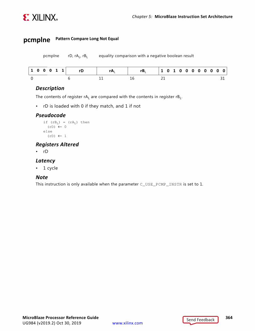
Chapter 5: MicroBlaze Instruction Set Architecture
pcmplne Pattern Compare Long Not Equal
pcmplne rD, rAL, rBL equality comparison with a negative boolean result
1 0 0 0 1 1 rD rAL rBL 1 0 1 0 0 0 0 0 0 0 0
0 6 11 16 21 31
DescriptionThe contents of register rAL are compared with the contents in register rBL.
• rD is loaded with 0 if they match, and 1 if not
Pseudocodeif (rBL) = (rAL) then(rD) ← 0
else(rD) ← 1
Registers Altered• rD
Latency• 1 cycle
NoteThis instruction is only available when the parameter C_USE_PCMP_INSTR is set to 1.
MicroBlaze Processor Reference Guide 364UG984 (v2019.2) Oct 30, 2019 www.xilinx.com
Send Feedback

Chapter 5: MicroBlaze Instruction Set Architecture
rsubl Arithmetic Reverse Subtract Long
rsubl rDL, rAL, rBL Subtract Long
rsublc rDL, rAL, rBL Subtract Long with Carry
rsublk rDL, rAL, rBL Subtract Long and Keep Carry
rsublkc rDL, rAL, rBL Subtract Long with Carry and Keep Carry
0 0 0 K C 1 rDL rAL rBL 0 0 1 0 0 0 0 0 0 0 0
0 6 11 16 21 31
DescriptionThe contents of register rAL are subtracted from the contents of register rBL and the result is placed into register rDL. Bit 3 of the instruction (labeled as K in the figure) is set to one for the mnemonic rsublk. Bit 4 of the instruction (labeled as C in the figure) is set to one for the mnemonic rsublc. Both bits are set to one for the mnemonic rsublkc.
When an rsubl instruction has bit 3 set (rsublk, rsublkc), the carry flag will Keep its previous value regardless of the outcome of the execution of the instruction. If bit 3 is cleared (rsubl, rsublc), then the carry flag will be affected by the execution of the instruction.
When bit 4 of the instruction is set to one (rsublc, rsublkc), the content of the carry flag (MSR[C]) affects the execution of the instruction. When bit 4 is cleared (rsubl, rsublk), the content of the carry flag does not affect the execution of the instruction (providing a normal subtraction).
Pseudocodeif C = 0 then(rDL) ← (rBL) + (rAL) + 1
else(rDL) ← (rBL) + (rAL) + MSR[C]
if K = 0 thenMSR[C] ← CarryOut64
Registers Altered• rDL
• MSR[C]
Latency• 1 cycle
NoteIn subtractions, Carry = (Borrow). When the Carry is set by a subtraction, it means that there is no Borrow, and when the Carry is cleared, it means that there is a Borrow.
MicroBlaze Processor Reference Guide 365UG984 (v2019.2) Oct 30, 2019 www.xilinx.com
Send Feedback
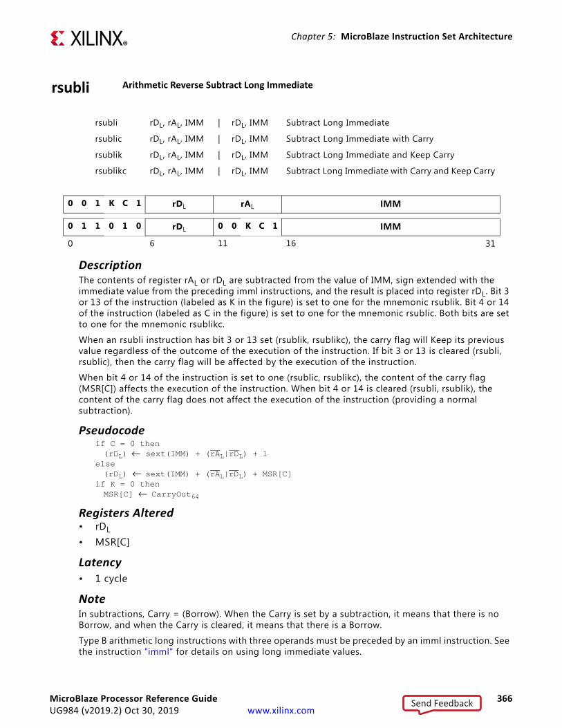
Chapter 5: MicroBlaze Instruction Set Architecture
rsubli Arithmetic Reverse Subtract Long Immediate
rsubli rDL, rAL, IMM | rDL, IMM Subtract Long Immediate
rsublic rDL, rAL, IMM | rDL, IMM Subtract Long Immediate with Carry
rsublik rDL, rAL, IMM | rDL, IMM Subtract Long Immediate and Keep Carry
rsublikc rDL, rAL, IMM | rDL, IMM Subtract Long Immediate with Carry and Keep Carry
0 0 1 K C 1 rDL rAL IMM
0 1 1 0 1 0 rDL 0 0 K C 1 IMM
0 6 11 16 31
DescriptionThe contents of register rAL or rDL are subtracted from the value of IMM, sign extended with the immediate value from the preceding imml instructions, and the result is placed into register rDL. Bit 3 or 13 of the instruction (labeled as K in the figure) is set to one for the mnemonic rsublik. Bit 4 or 14 of the instruction (labeled as C in the figure) is set to one for the mnemonic rsublic. Both bits are set to one for the mnemonic rsublikc.
When an rsubli instruction has bit 3 or 13 set (rsublik, rsublikc), the carry flag will Keep its previous value regardless of the outcome of the execution of the instruction. If bit 3 or 13 is cleared (rsubli, rsublic), then the carry flag will be affected by the execution of the instruction.
When bit 4 or 14 of the instruction is set to one (rsublic, rsublikc), the content of the carry flag (MSR[C]) affects the execution of the instruction. When bit 4 or 14 is cleared (rsubli, rsublik), the content of the carry flag does not affect the execution of the instruction (providing a normal subtraction).
Pseudocodeif C = 0 then(rDL) ← sext(IMM) + (rAL|rDL) + 1
else(rDL) ← sext(IMM) + (rAL|rDL) + MSR[C]
if K = 0 thenMSR[C] ← CarryOut64
Registers Altered• rDL
• MSR[C]
Latency• 1 cycle
NoteIn subtractions, Carry = (Borrow). When the Carry is set by a subtraction, it means that there is no Borrow, and when the Carry is cleared, it means that there is a Borrow.
Type B arithmetic long instructions with three operands must be preceded by an imml instruction. See the instruction “imml” for details on using long immediate values.
MicroBlaze Processor Reference Guide 366UG984 (v2019.2) Oct 30, 2019 www.xilinx.com
Send Feedback
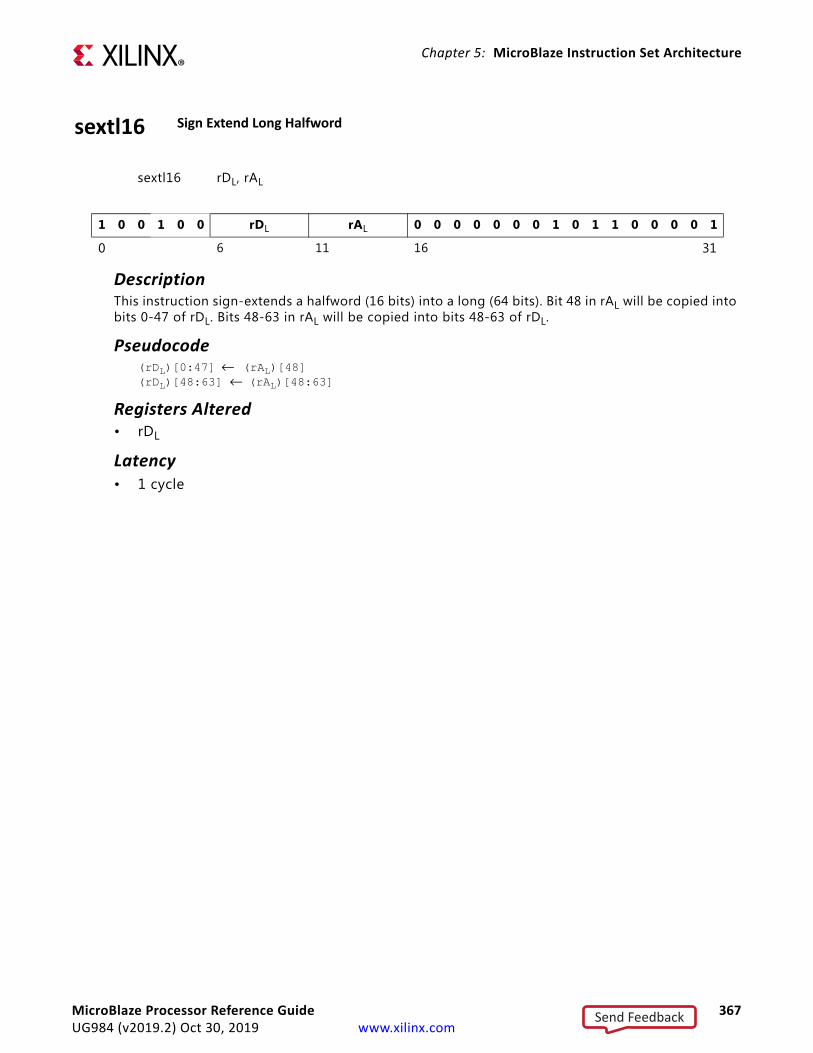
Chapter 5: MicroBlaze Instruction Set Architecture
sextl16 Sign Extend Long Halfword
sextl16 rDL, rAL
1 0 0 1 0 0 rDL rAL 0 0 0 0 0 0 0 1 0 1 1 0 0 0 0 1
0 6 11 16 31
DescriptionThis instruction sign-extends a halfword (16 bits) into a long (64 bits). Bit 48 in rAL will be copied into bits 0-47 of rDL. Bits 48-63 in rAL will be copied into bits 48-63 of rDL.
Pseudocode(rDL)[0:47] ← (rAL)[48] (rDL)[48:63] ← (rAL)[48:63]
Registers Altered• rDL
Latency• 1 cycle
MicroBlaze Processor Reference Guide 367UG984 (v2019.2) Oct 30, 2019 www.xilinx.com
Send Feedback

Chapter 5: MicroBlaze Instruction Set Architecture
sextl32 Sign Extend Long Word
sextl32 rDL, rAL
1 0 0 1 0 0 rDL rAL 0 0 0 0 0 0 0 1 0 1 1 0 0 0 1 0
0 6 11 16 31
DescriptionThis instruction sign-extends a word (32 bits) into a long (64 bits). Bit 32 in rAL will be copied into bits 0-31 of rDL. Bits 32-63 in rAL will be copied into bits 32-63 of rDL.
Pseudocode(rDL)[0:31] ← (rAL)[32] (rDL)[32:63] ← (rAL)[32:63]
Registers Altered• rDL
Latency• 1 cycle
MicroBlaze Processor Reference Guide 368UG984 (v2019.2) Oct 30, 2019 www.xilinx.com
Send Feedback
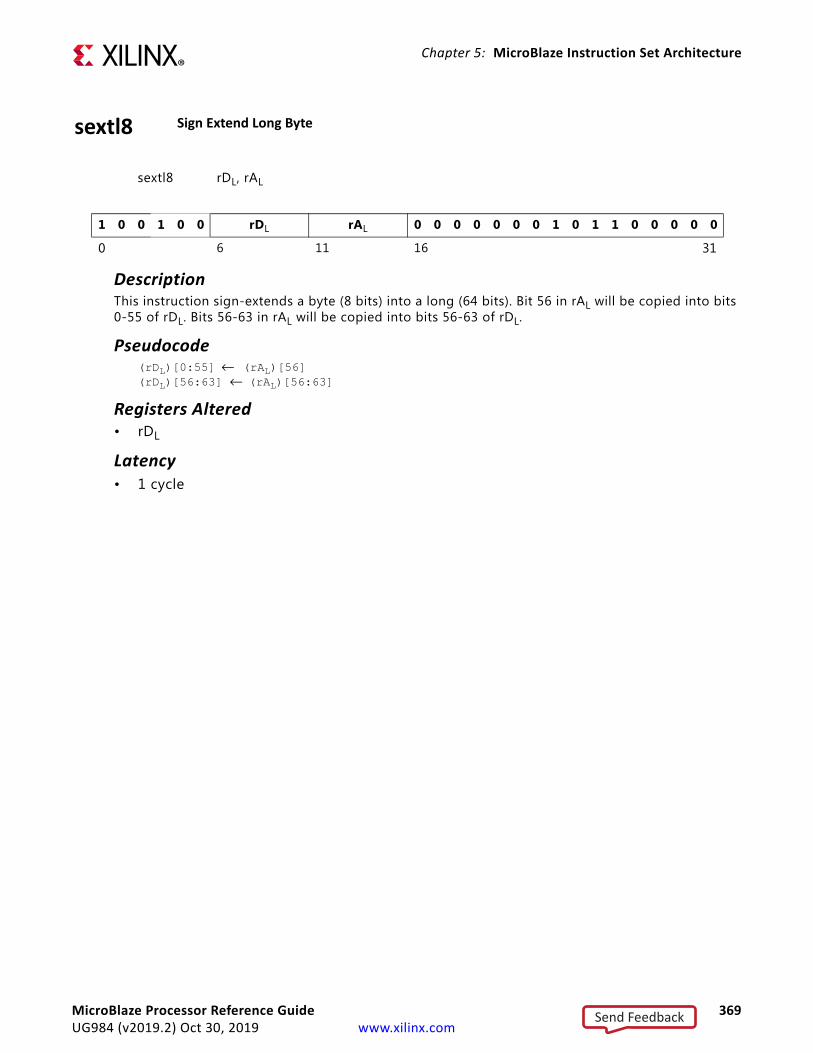
Chapter 5: MicroBlaze Instruction Set Architecture
sextl8 Sign Extend Long Byte
sextl8 rDL, rAL
1 0 0 1 0 0 rDL rAL 0 0 0 0 0 0 0 1 0 1 1 0 0 0 0 0
0 6 11 16 31
DescriptionThis instruction sign-extends a byte (8 bits) into a long (64 bits). Bit 56 in rAL will be copied into bits 0-55 of rDL. Bits 56-63 in rAL will be copied into bits 56-63 of rDL.
Pseudocode(rDL)[0:55] ← (rAL)[56] (rDL)[56:63] ← (rAL)[56:63]
Registers Altered• rDL
Latency• 1 cycle
MicroBlaze Processor Reference Guide 369UG984 (v2019.2) Oct 30, 2019 www.xilinx.com
Send Feedback
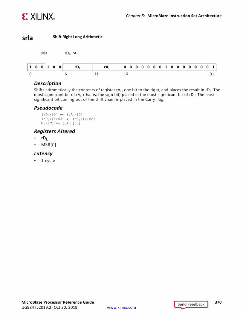
Chapter 5: MicroBlaze Instruction Set Architecture
srla Shift Right Long Arithmetic
srla rDL, rAL
1 0 0 1 0 0 rDL rAL 0 0 0 0 0 0 0 1 0 0 0 0 0 0 0 1
0 6 11 16 31
DescriptionShifts arithmetically the contents of register rAL, one bit to the right, and places the result in rDL. The most significant bit of rAL (that is, the sign bit) placed in the most significant bit of rDL. The least significant bit coming out of the shift chain is placed in the Carry flag.
Pseudocode(rDL)[0] ← (rAL)[0] (rDL)[1:63] ← (rAL)[0:62] MSR[C] ← (rAL)[63]
Registers Altered• rDL
• MSR[C]
Latency• 1 cycle
MicroBlaze Processor Reference Guide 370UG984 (v2019.2) Oct 30, 2019 www.xilinx.com
Send Feedback

Chapter 5: MicroBlaze Instruction Set Architecture
srlc Shift Right Long with Carry
srlc rDL, rAL
1 0 0 1 0 0 rDL rAL 0 0 0 0 0 0 0 1 0 0 1 0 0 0 0 1
0 6 11 16 31
DescriptionShifts the contents of register rAL, one bit to the right, and places the result in rDL. The Carry flag is shifted in the shift chain and placed in the most significant bit of rDL. The least significant bit coming out of the shift chain is placed in the Carry flag.
Pseudocode(rDL)[0] ← MSR[C] (rDL)[1:63] ← (rAL)[0:62] MSR[C] ← (rAL)[63]
Registers Altered• rDL
• MSR[C]
Latency• 1 cycle
MicroBlaze Processor Reference Guide 371UG984 (v2019.2) Oct 30, 2019 www.xilinx.com
Send Feedback

Chapter 5: MicroBlaze Instruction Set Architecture
srll Shift Right Long Logical
srll rDL, rAL
1 0 0 1 0 0 rDL rAL 0 0 0 0 0 0 0 1 0 1 0 0 0 0 0 1
0 6 11 16 31
DescriptionShifts logically the contents of register rAL, one bit to the right, and places the result in rDL. A zero is shifted in the shift chain and placed in the most significant bit of rDL. The least significant bit coming out of the shift chain is placed in the Carry flag.
Pseudocode(rDL)[0] ← 0 (rDL)[1:63] ← (rAL)[0:62] MSR[C] ← (rAL)[63]
Registers Altered• rDL
• MSR[C]
Latency• 1 cycle
MicroBlaze Processor Reference Guide 372UG984 (v2019.2) Oct 30, 2019 www.xilinx.com
Send Feedback
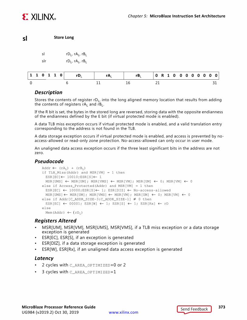
Chapter 5: MicroBlaze Instruction Set Architecture
sl Store Long
sl rDL, rAL, rBL
slr rDL, rAL, rBL
1 1 0 1 1 0 rDL rAL rBL 0 R 1 0 0 0 0 0 0 0 0
0 6 11 16 21 31
DescriptionStores the contents of register rDL, into the long aligned memory location that results from adding the contents of registers rAL and rBL.
If the R bit is set, the bytes in the stored long are reversed, storing data with the opposite endianness of the endianness defined by the E bit (if virtual protected mode is enabled).
A data TLB miss exception occurs if virtual protected mode is enabled, and a valid translation entry corresponding to the address is not found in the TLB.
A data storage exception occurs if virtual protected mode is enabled, and access is prevented by no-access-allowed or read-only zone protection. No-access-allowed can only occur in user mode.
An unaligned data access exception occurs if the three least significant bits in the address are not zero.
PseudocodeAddr ← (rAL) + (rBL) if TLB_Miss(Addr) and MSR[VM] = 1 thenESR[EC]← 10010;ESR[S]← 1MSR[UMS] ← MSR[UM]; MSR[VMS] ← MSR[VM]; MSR[UM] ← 0; MSR[VM] ← 0
else if Access_Protected(Addr) and MSR[VM] = 1 thenESR[EC] ← 10000;ESR[S]← 1; ESR[DIZ] ← No-access-allowedMSR[UMS]← MSR[UM]; MSR[VMS] ← MSR[VM]; MSR[UM] ← 0; MSR[VM] ← 0
else if Addr[C_ADDR_SIZE-3:C_ADDR_SIZE-1] ≠ 0 thenESR[EC] ← 00001; ESR[W] ← 1; ESR[S] ← 1; ESR[Rx] ← rD
else Mem(Addr) ← (rDL)
Registers Altered• MSR[UM], MSR[VM], MSR[UMS], MSR[VMS], if a TLB miss exception or a data storage
exception is generated• ESR[EC], ESR[S], if an exception is generated• ESR[DIZ], if a data storage exception is generated• ESR[W], ESR[Rx], if an unaligned data access exception is generated
Latency• 2 cycles with C_AREA_OPTIMIZED=0 or 2• 3 cycles with C_AREA_OPTIMIZED=1
MicroBlaze Processor Reference Guide 373UG984 (v2019.2) Oct 30, 2019 www.xilinx.com
Send Feedback
Chapter 5: MicroBlaze Instruction Set Architecture
NotesThe long reversed instruction is only valid if MicroBlaze is configured to use reorder instructions (C_USE_REORDER_INSTR = 1).
MicroBlaze Processor Reference Guide 374UG984 (v2019.2) Oct 30, 2019 www.xilinx.com
Send Feedback
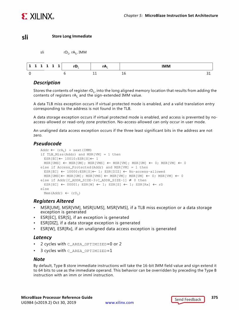
Chapter 5: MicroBlaze Instruction Set Architecture
sli Store Long Immediate
sli rDL, rAL, IMM
1 1 1 1 1 1 rDL rAL IMM
0 6 11 16 31
DescriptionStores the contents of register rDL, into the long aligned memory location that results from adding the contents of registers rAL and the sign-extended IMM value.
A data TLB miss exception occurs if virtual protected mode is enabled, and a valid translation entry corresponding to the address is not found in the TLB.
A data storage exception occurs if virtual protected mode is enabled, and access is prevented by no-access-allowed or read-only zone protection. No-access-allowed can only occur in user mode.
An unaligned data access exception occurs if the three least significant bits in the address are not zero.
PseudocodeAddr ← (rAL) + sext(IMM) if TLB_Miss(Addr) and MSR[VM] = 1 thenESR[EC]← 10010;ESR[S]← 1MSR[UMS] ← MSR[UM]; MSR[VMS] ← MSR[VM]; MSR[UM] ← 0; MSR[VM] ← 0
else if Access_Protected(Addr) and MSR[VM] = 1 thenESR[EC] ← 10000;ESR[S]← 1; ESR[DIZ] ← No-access-allowedMSR[UMS]← MSR[UM]; MSR[VMS] ← MSR[VM]; MSR[UM] ← 0; MSR[VM] ← 0
else if Addr[C_ADDR_SIZE-3:C_ADDR_SIZE-1] ≠ 0 thenESR[EC] ← 00001; ESR[W] ← 1; ESR[S] ← 1; ESR[Rx] ← rD
else Mem(Addr) ← (rDL)
Registers Altered• MSR[UM], MSR[VM], MSR[UMS], MSR[VMS], if a TLB miss exception or a data storage
exception is generated• ESR[EC], ESR[S], if an exception is generated• ESR[DIZ], if a data storage exception is generated• ESR[W], ESR[Rx], if an unaligned data access exception is generated
Latency• 2 cycles with C_AREA_OPTIMIZED=0 or 2• 3 cycles with C_AREA_OPTIMIZED=1
NoteBy default, Type B store immediate instructions will take the 16-bit IMM field value and sign extend it to 64 bits to use as the immediate operand. This behavior can be overridden by preceding the Type B instruction with an imm or imml instruction.
MicroBlaze Processor Reference Guide 375UG984 (v2019.2) Oct 30, 2019 www.xilinx.com
Send Feedback

Chapter 5: MicroBlaze Instruction Set Architecture
xorl Logical Exclusive OR Long
xorl rDL, rAL, rBL
1 0 0 0 1 0 rDL rAL rBL 0 0 1 0 0 0 0 0 0 0 0
0 6 11 16 21 31
DescriptionThe contents of register rAL are XORed with the contents of register rBL; the result is placed into register rDL.
Pseudocode(rDL) ← (rAL) ⊕ (rBL)
Registers Altered• rDL
Latency• 1 cycle
MicroBlaze Processor Reference Guide 376UG984 (v2019.2) Oct 30, 2019 www.xilinx.com
Send Feedback

Chapter 5: MicroBlaze Instruction Set Architecture
xorli Logical Exclusive OR Long with Immediate
xorli rDL, rAL, IMM | rDL, IMM
1 0 1 0 1 0 rDL rAL IMM
0 1 1 0 1 0 rDL 1 0 0 1 0 IMM
0 6 11 16 31
DescriptionThe contents of register rAL or rDL are XOR’ed with the IMM field, sign extended with the immediate value from the preceding imml instructions; the result is placed into register rDL.
Pseudocode(rDL) ← (rAL|rDL) ⊕ sext(IMM24 & IMM)
Registers Altered• rDL
Latency• 1 cycle
NotesType B logical long instructions with three operands must be preceded by an imml instruction. See the instruction “imml” for details on using long immediate values.
MicroBlaze Processor Reference Guide 377UG984 (v2019.2) Oct 30, 2019 www.xilinx.com
Send Feedback
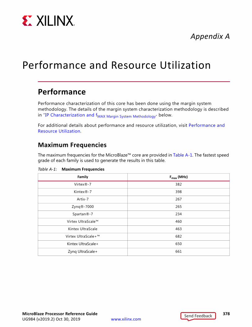
Appendix A
Performance and Resource Utilization
PerformancePerformance characterization of this core has been done using the margin system methodology. The details of the margin system characterization methodology is described in “IP Characterization and fMAX Margin System Methodology” below.
For additional details about performance and resource utilization, visit Performance and Resource Utilization.
Maximum FrequenciesThe maximum frequencies for the MicroBlaze™ core are provided in Table A-1. The fastest speed grade of each family is used to generate the results in this table.
Table A-1: Maximum Frequencies
Family Fmax (MHz)
Virtex®-7 382
Kintex®-7 398
Artix-7 267
Zynq®-7000 265
Spartan®-7 234
Virtex UltraScale™ 460
Kintex UltraScale 463
Virtex UltraScale+™ 682
Kintex UltraScale+ 650
Zynq UltraScale+ 661
MicroBlaze Processor Reference Guide 378UG984 (v2019.2) Oct 30, 2019 www.xilinx.com
Send Feedback

Appendix A: Performance and Resource Utilization
Resource UtilizationThe MicroBlaze core resource utilization for various parameter configurations are measured for the following devices:
• Virtex-7 (Table A-2)
• Kintex-7 (Table A-3)
• Artix-7 (Table A-4)
• Zynq-7000 (Table A-5)
• Spartan-7 (Table A-6)
• Virtex UltraScale (Table A-7)
• Kintex UltraScale (Table A-8)
• Virtex UltraScale+ (Table A-9)
• Kintex UltraScale+ (Table A-10)
• Zynq UltraScale+ (Table A-11)
The parameter values for each of the measured configurations are shown in Table A-12. The configurations directly correspond to the predefined presets and templates in the MicroBlaze Configuration Wizard, defined for the 32-bit processor implementation.
The 32-bit processor implementation data uses the parameters C_DATA_SIZE = 32 and C_ADDR_SIZE = 32, whereas the 64-bit processor implementation data uses the parameters C_DATA_SIZE = 64 and C_ADDR_SIZE = 48.
Table A-2: Device Utilization - Virtex-7 FPGAs (XC7VX485T ffg1761-3)
Configuration
Device Resources
32-bit 64-bit
LUTs FFs BRAMs(36K)
Fmax(MHz) LUTs FFs BRAMs
(36K)Fmax
(MHz)
Microcontroller Preset 1173 811 0 308 2139 1262 0 286
Real-time Preset 2484 2121 6 245 3793 3150 6 241
Application Preset 4340 3807 19 212 6492 4919 19 165
Minimum Area 629 230 0 382 1133 400 0 329
Maximum Performance 4096 3210 19 218 6813 4778 20 172
Maximum Frequency 915 553 0 382 1815 858 0 329
Linux with MMU 3512 3126 11 213 5084 4496 16 198
Low-end Linux with MMU 2986 2511 7 233 4519 3726 10 207
Typical 2007 1680 6 253 3389 2498 8 251
Frequency Optimized 6011 5791 14 252 9398 8735 15 168
MicroBlaze Processor Reference Guide 379UG984 (v2019.2) Oct 30, 2019 www.xilinx.com
Send Feedback

Appendix A: Performance and Resource Utilization
Table A-3: Device Utilization - Kintex-7 FPGAs (XC7K325T ffg900-3)
Configuration
Device Resources
32-bit 64-bit
LUTs FFs BRAMs(36K)
Fmax(MHz) LUTs FFs BRAMs
(36K)Fmax
(MHz)
Microcontroller Preset 1176 811 0 318 2129 1226 0 287
Real-time Preset 2477 2121 6 246 3792 3151 6 220
Application Preset 4368 3779 19 214 6479 4899 19 174
Minimum Area 637 234 0 398 1146 398 0 330
Maximum Performance 4129 3207 19 222 6816 4778 20 171
Maximum Frequency 908 553 0 398 1817 862 0 330
Linux with MMU 3507 3149 11 206 5088 4493 16 205
Low-end Linux with MMU 2986 2537 7 213 4521 3708 10 202
Typical 2017 1679 6 257 3404 2496 8 252
Frequency Optimized 6004 5874 14 263 9425 8765 15 172
Table A-4: Device Utilization - Artix-7 FPGAs (XC7A200T fbg676-3)
Configuration
Device Resources
32-bit 64-bit
LUTs FFs BRAMs(36K)
Fmax(MHz) LUTs FFs BRAMs
(36K)Fmax
(MHz)
Microcontroller Preset 1174 811 0 218 2145 1226 0 187
Real-time Preset 2467 2121 6 177 3797 3153 6 178
Application Preset 4326 3747 19 149 6461 4891 19 136
Minimum Area 625 227 0 267 1141 397 0 221
Maximum Performance 4106 3208 19 153 6802 4799 20 142
Maximum Frequency 911 553 0 267 1815 858 0 221
Linux with MMU 3515 3122 11 150 5081 4492 16 139
Low-end Linux with MMU 2987 2506 7 151 4490 3711 10 136
Typical 2014 1682 6 187 3398 2500 8 190
Frequency Optimized 5956 5787 14 166 9366 8725 15 137
MicroBlaze Processor Reference Guide 380UG984 (v2019.2) Oct 30, 2019 www.xilinx.com
Send Feedback

Appendix A: Performance and Resource Utilization
Table A-5: Device Utilization - Zynq-7000 FPGAs (XC7Z020 clg484-3)
Configuration
Device Resources
32-bit 64-bit
LUTs FFs BRAMs(36K)
Fmax(MHz) LUTs FFs BRAMs
(36K)Fmax
(MHz)
Microcontroller Preset 1174 811 0 221 2148 1226 0 191
Real-time Preset 2465 2120 6 176 3785 3156 6 178
Application Preset 4345 3744 19 148 6496 4979 19 141
Minimum Area 626 226 0 265 1138 400 0 222
Maximum Performance 4105 3197 19 152 6791 4760 20 138
Maximum Frequency 908 553 0 265 1813 858 0 222
Linux with MMU 3507 3125 11 147 5086 4489 16 135
Low-end Linux with MMU 2988 2506 7 159 4489 3711 10 138
Typical 2021 1680 6 191 3416 2501 8 192
Frequency Optimized 5953 5785 14 176 9381 8724 15 134
Table A-6: Device Utilization - Spartan-7 FPGAs (XC7S25 csga225-2)
Configuration
Device Resources
32-bit 64-bit
LUTs FFs BRAMs(36K)
Fmax(MHz) LUTs FFs BRAMs
(36K)Fmax
(MHz)
Microcontroller Preset 1175 811 0 188 2134 1226 0 161
Real-time Preset 2461 2125 6 161 3810 3151 6 148
Application Preset 4342 3812 19 130 6465 4872 19 120
Minimum Area 625 225 0 234 1145 406 0 199
Maximum Performance 4085 3197 19 134 6779 4757 20 118
Maximum Frequency 909 553 0 234 1816 858 0 199
Linux with MMU 3505 3128 11 133 5077 4490 16 118
Low-end Linux with MMU 2980 2509 7 144 4466 3709 10 122
Typical 2020 1680 6 168 3406 2492 8 160
Frequency Optimized 5955 5783 14 154 9363 8724 15 119
MicroBlaze Processor Reference Guide 381UG984 (v2019.2) Oct 30, 2019 www.xilinx.com
Send Feedback

Appendix A: Performance and Resource Utilization
Table A-7: Device Utilization - Virtex UltraScale FPGAs (XCVU095 ffvd1924-3)
Configuration
Device Resources
32-bit 64-bit
LUTs FFs BRAMs(36K)
Fmax(MHz) LUTs FFs BRAMs
(36K)Fmax
(MHz)
Microcontroller Preset 1105 821 0 413 2090 1226 0 345
Real-time Preset 2520 2121 6 295 3822 3158 6 293
Application Preset 4355 3801 19 262 6617 4826 19 238
Minimum Area 567 231 0 460 991 415 0 374
Maximum Performance 4102 3208 19 286 6936 4776 20 244
Maximum Frequency 913 553 0 460 1817 860 0 374
Linux with MMU 3523 3221 11 258 5149 4511 16 239
Low-end Linux with MMU 3002 2518 7 271 4559 3728 10 234
Typical 2035 1680 6 316 3482 2497 8 307
Frequency Optimized 6150 5806 14 301 9579 8814 15 240
Table A-8: Device Utilization - Kintex UltraScale FPGAs (XCKU040 ffva1156-3)
Configuration
Device Resources
32-bit 64-bit
LUTs FFs BRAMs(36K)
Fmax(MHz) LUTs FFs BRAMs
(36K)Fmax
(MHz)
Microcontroller Preset 1106 811 0 417 2046 1261 0 352
Real-time Preset 2507 2119 6 300 3820 3155 6 302
Application Preset 4336 3760 19 255 6621 4961 19 233
Minimum Area 578 240 0 463 988 401 0 391
Maximum Performance 4117 3209 19 285 6943 4784 20 249
Maximum Frequency 913 556 0 463 1832 869 0 391
Linux with MMU 3502 3129 11 247 5142 4492 16 239
Low-end Linux with MMU 2997 2507 7 267 4560 3745 10 233
Typical 2033 1683 6 319 3471 2505 8 313
Frequency Optimized 6172 5837 14 307 9574 8777 15 243
MicroBlaze Processor Reference Guide 382UG984 (v2019.2) Oct 30, 2019 www.xilinx.com
Send Feedback

Appendix A: Performance and Resource Utilization
Table A-9: Device Utilization - Virtex UltraScale+ FPGAs (XCVU3P ffvc1517-3)
Configuration
Device Resources
32-bit 64-bit
LUTs FFs BRAMs(36K)
Fmax(MHz) LUTs FFs BRAMs
(36K)Fmax
(MHz)
Microcontroller Preset 1107 823 0 573 2063 1226 0 462
Real-time Preset 2543 2122 6 399 3911 3156 6 389
Application Preset 4403 3745 19 360 6679 4872 19 333
Minimum Area 563 225 0 682 991 397 0 602
Maximum Performance 4207 3208 19 371 7044 4772 20 330
Maximum Frequency 910 553 0 682 1816 858 0 602
Linux with MMU 3553 3129 11 350 5213 4486 16 333
Low-end Linux with MMU 3020 2508 7 374 4595 3705 10 333
Typical 2064 1679 6 433 3492 2496 8 427
Frequency Optimized 6227 5789 14 416 9649 8773 15 344
Table A-10: Device Utilization - Kintex UltraScale+ FPGAs (XCKU15P ffva1156-3)
Configuration
Device Resources
32-bit 64-bit
LUTs FFs BRAMs(36K)
Fmax(MHz) LUTs FFs BRAMs
(36K)Fmax
(MHz)
Microcontroller Preset 1105 811 0 573 2049 1226 0 522
Real-time Preset 2449 2122 6 416 3914 3151 6 407
Application Preset 4404 3744 19 349 6693 4873 19 341
Minimum Area 566 225 0 650 996 397 0 602
Maximum Performance 4209 3237 19 371 7045 4778 20 340
Maximum Frequency 915 553 0 650 1814 858 0 602
Linux with MMU 3554 3190 11 351 5216 4491 16 323
Low-end Linux with MMU 3023 2507 7 365 4598 3712 10 344
Typical 2067 1681 6 441 3489 2493 8 421
Frequency Optimized 6223 5787 14 433 9652 8766 15 340
MicroBlaze Processor Reference Guide 383UG984 (v2019.2) Oct 30, 2019 www.xilinx.com
Send Feedback

Appendix A: Performance and Resource Utilization
Table A-11: Device Utilization - Zynq UltraScale+ FPGAs (XCZU9EG ffvb1156-3)
Configuration
Device Resources
32-bit 64-bit
LUTs FFs BRAMs(36K)
Fmax(MHz) LUTs FFs BRAMs
(36K)Fmax
(MHz)
Microcontroller Preset 1112 822 0 561 2046 1226 0 476
Real-time Preset 2540 2120 6 409 3912 3150 6 388
Application Preset 4415 3743 19 346 6684 4888 19 336
Minimum Area 566 229 0 661 995 407 0 573
Maximum Performance 4212 3207 19 372 7027 4779 20 336
Maximum Frequency 908 553 0 661 1818 858 0 573
Linux with MMU 3552 3121 11 338 5227 4553 16 335
Low-end Linux with MMU 3018 2501 7 369 4597 3703 10 319
Typical 2068 1681 6 430 3490 2493 8 428
Frequency Optimized 6248 5819 14 413 9647 8781 15 348
MicroBlaze Processor Reference Guide 384UG984 (v2019.2) Oct 30, 2019 www.xilinx.com
Send Feedback
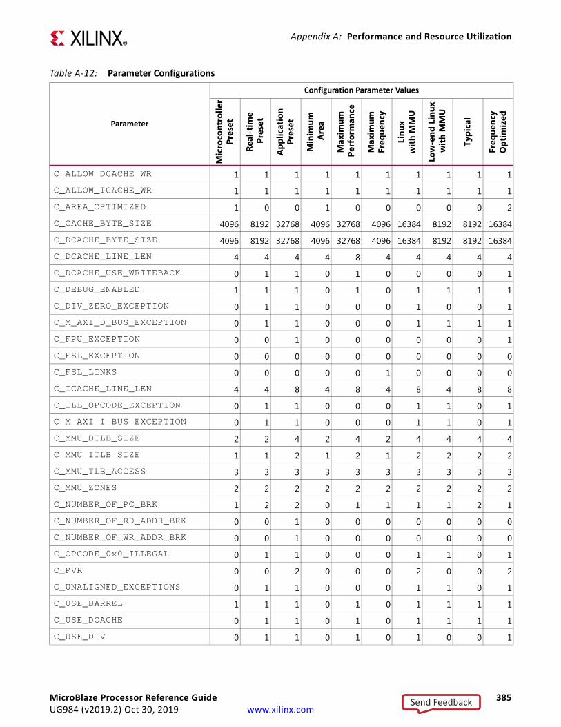
Appendix A: Performance and Resource Utilization
Table A-12: Parameter Configurations
Parameter
Configuration Parameter Values
Mic
roco
ntro
ller
Pres
et
Real
-tim
e P
rese
t
App
licat
ion
Pres
et
Min
imum
Are
a
Max
imum
Per
form
ance
Max
imum
Fr
eque
ncy
Linu
x w
ith
MM
U
Low
-end
Lin
ux w
ith
MM
U
Typi
cal
Freq
uenc
yO
ptim
ized
C_ALLOW_DCACHE_WR 1 1 1 1 1 1 1 1 1 1
C_ALLOW_ICACHE_WR 1 1 1 1 1 1 1 1 1 1
C_AREA_OPTIMIZED 1 0 0 1 0 0 0 0 0 2
C_CACHE_BYTE_SIZE 4096 8192 32768 4096 32768 4096 16384 8192 8192 16384
C_DCACHE_BYTE_SIZE 4096 8192 32768 4096 32768 4096 16384 8192 8192 16384
C_DCACHE_LINE_LEN 4 4 4 4 8 4 4 4 4 4
C_DCACHE_USE_WRITEBACK 0 1 1 0 1 0 0 0 0 1
C_DEBUG_ENABLED 1 1 1 0 1 0 1 1 1 1
C_DIV_ZERO_EXCEPTION 0 1 1 0 0 0 1 0 0 1
C_M_AXI_D_BUS_EXCEPTION 0 1 1 0 0 0 1 1 1 1
C_FPU_EXCEPTION 0 0 1 0 0 0 0 0 0 1
C_FSL_EXCEPTION 0 0 0 0 0 0 0 0 0 0
C_FSL_LINKS 0 0 0 0 0 1 0 0 0 0
C_ICACHE_LINE_LEN 4 4 8 4 8 4 8 4 8 8
C_ILL_OPCODE_EXCEPTION 0 1 1 0 0 0 1 1 0 1
C_M_AXI_I_BUS_EXCEPTION 0 1 1 0 0 0 1 1 0 1
C_MMU_DTLB_SIZE 2 2 4 2 4 2 4 4 4 4
C_MMU_ITLB_SIZE 1 1 2 1 2 1 2 2 2 2
C_MMU_TLB_ACCESS 3 3 3 3 3 3 3 3 3 3
C_MMU_ZONES 2 2 2 2 2 2 2 2 2 2
C_NUMBER_OF_PC_BRK 1 2 2 0 1 1 1 1 2 1
C_NUMBER_OF_RD_ADDR_BRK 0 0 1 0 0 0 0 0 0 0
C_NUMBER_OF_WR_ADDR_BRK 0 0 1 0 0 0 0 0 0 0
C_OPCODE_0x0_ILLEGAL 0 1 1 0 0 0 1 1 0 1
C_PVR 0 0 2 0 0 0 2 0 0 2
C_UNALIGNED_EXCEPTIONS 0 1 1 0 0 0 1 1 0 1
C_USE_BARREL 1 1 1 0 1 0 1 1 1 1
C_USE_DCACHE 0 1 1 0 1 0 1 1 1 1
C_USE_DIV 0 1 1 0 1 0 1 0 0 1
MicroBlaze Processor Reference Guide 385UG984 (v2019.2) Oct 30, 2019 www.xilinx.com
Send Feedback
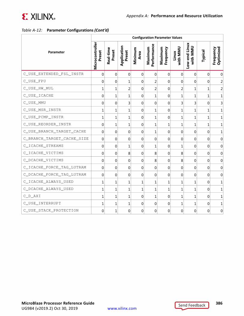
Appendix A: Performance and Resource Utilization
C_USE_EXTENDED_FSL_INSTR 0 0 0 0 0 0 0 0 0 0
C_USE_FPU 0 0 1 0 2 0 0 0 0 2
C_USE_HW_MUL 1 1 2 0 2 0 2 1 1 2
C_USE_ICACHE 0 1 1 0 1 0 1 1 1 1
C_USE_MMU 0 0 3 0 0 0 3 3 0 3
C_USE_MSR_INSTR 1 1 1 0 1 0 1 1 1 1
C_USE_PCMP_INSTR 1 1 1 0 1 0 1 1 1 1
C_USE_REORDER_INSTR 0 1 1 0 1 1 1 1 1 1
C_USE_BRANCH_TARGET_CACHE 0 0 0 0 1 0 0 0 0 1
C_BRANCH_TARGET_CACHE_SIZE 0 0 0 0 0 0 0 0 0 0
C_ICACHE_STREAMS 0 0 1 0 1 0 1 0 0 0
C_ICACHE_VICTIMS 0 0 8 0 8 0 8 0 0 0
C_DCACHE_VICTIMS 0 0 0 0 8 0 8 0 0 0
C_ICACHE_FORCE_TAG_LUTRAM 0 0 0 0 0 0 0 0 0 0
C_DCACHE_FORCE_TAG_LUTRAM 0 0 0 0 0 0 0 0 0 0
C_ICACHE_ALWAYS_USED 1 1 1 1 1 1 1 1 0 1
C_DCACHE_ALWAYS_USED 1 1 1 1 1 1 1 1 0 1
C_D_AXI 1 1 1 0 1 0 1 1 0 1
C_USE_INTERRUPT 1 1 1 0 0 0 1 1 0 1
C_USE_STACK_PROTECTION 0 1 0 0 0 0 0 0 0 0
Table A-12: Parameter Configurations (Cont’d)
Parameter
Configuration Parameter Values
Mic
roco
ntro
ller
Pres
et
Real
-tim
e P
rese
t
App
licat
ion
Pres
et
Min
imum
Are
a
Max
imum
Per
form
ance
Max
imum
Fr
eque
ncy
Linu
x w
ith
MM
U
Low
-end
Lin
ux w
ith
MM
U
Typi
cal
Freq
uenc
yO
ptim
ized
MicroBlaze Processor Reference Guide 386UG984 (v2019.2) Oct 30, 2019 www.xilinx.com
Send Feedback
Appendix A: Performance and Resource Utilization
IP Characterization and fMAX Margin System Methodology
IntroductionThis section describes the methods to determine the maximum frequency (FMAX) of IP operation within a system design. The method enables realistic performance reporting for any Xilinx FPGA architecture. The maximum frequency of a design is the maximum frequency at which the overall system can be implemented without encountering timing issues.
The FMAX Margin System MethodologyIt is important to determine the IP performance in the context of a user system. In the case of the MicroBlaze characterization, the system includes the following items:
• The IP under test (MicroBlaze Processor)
• Local Memory (LMB)
• One level of Interconnect (AXI4, AXI4-Lite, AXI4-Stream)
• Memory controller (EMC)
• On-chip BRAM controller
• Peripherals (UART, Timer, Interrupt Controller, MDM)
Determining the FMAX of an Embedded IP with these components provides a more realistic performance target.
The system above has three types of AXI Interconnect. AXI4-Lite used for peripheral command and control, AXI4 used for memory accesses, and AXI4-Stream used for MicroBlaze streams.
For FMAX Margin System Analysis, the clock frequency of the system is incremented up to the maximum frequency where the system breaks with timing violations (worst case negative slack). The reported frequency is the failing frequency subtracted with this worst case negative slack.
Tool Options and Other FactorsXilinx tools offer a number of options and settings that provide a trade-off between design performance, resource usage, implementation run time, and memory footprint. The settings that produce the best results for one design might not necessarily work for another design.
For the purpose of the FMAX Margin System Analysis, the IP design is characterized with default settings without specific constraints (other than the clocking constraint). This analysis is done with all different FPGA architectures and the maximum speed grade.
MicroBlaze Processor Reference Guide 387UG984 (v2019.2) Oct 30, 2019 www.xilinx.com
Send Feedback

Appendix B
Additional Resources and Legal Notices
Xilinx ResourcesFor support resources such as Answers, Documentation, Downloads, and Forums, see Xilinx Support.
Solution CentersSee the Xilinx Solution Centers for support on devices, software tools, and intellectual property at all stages of the design cycle. Topics include design assistance, advisories, and troubleshooting tips.
Documentation Navigator and Design HubsXilinx® Documentation Navigator provides access to Xilinx documents, videos, and support resources, which you can filter and search to find information. To open the Xilinx Documentation Navigator (DocNav):
• From the Vivado® IDE, select Help > Documentation and Tutorials.
• On Windows, select Start > All Programs > Xilinx Design Tools > DocNav.
• At the Linux command prompt, enter docnav.
Xilinx Design Hubs provide links to documentation organized by design tasks and other topics, which you can use to learn key concepts and address frequently asked questions. To access the Design Hubs:
• In the Xilinx Documentation Navigator, click the Design Hubs View tab.
• On the Xilinx website, see the Design Hubs page.
Note: For more information on Documentation Navigator, see the Documentation Navigator page on the Xilinx website.
MicroBlaze Processor Reference Guide 388UG984 (v2019.2) Oct 30, 2019 www.xilinx.com
Send Feedback

Appendix B: Additional Resources and Legal Notices
ReferencesThe following documents are available using your Vivado® installation.
Relevant individual documents are linked below.
1. PowerPC Processor Reference Guide (UG011)
2. Soft Error Mitigation Controller LogiCORE IP Product Guide (PG036)
3. LMB BRAM Interface Controller LogiCORE IP Product Guide (PG112)
4. MicroBlaze Debug Module (MDM) Product Guide (PG115)
5. Device Reliability Report User Guide (UG116)
6. System Cache LogiCORE IP Product Guide (PG118)
7. Triple Modular Redundancy (TMR) Subsystem Product Guide (PG268)
8. Hierarchical Design Methodology Guide (UG748)
9. Vitis Unified Software Platform Documentation (UG1416)
10. Vivado Design Suite User Guide: Designing With IP (UG896)
11. Vivado Design Suite User Guide: Embedded Processor Hardware Design (UG898)
12. Vivado Design Suite User Guide: Designing IP Subsystems Using IP Integrator (UG994)
13. Embedded System Tools Reference Manual (UG1043)
14. AMBA 4 AXI4-Stream Protocol Specification, Version 1.0 (Arm IHI 0051A)
15. AMBA AXI and ACE Protocol Specification (Arm IHI 0022E)
16. UltraScale Architecture Soft Error Mitigation Controller LogiCORE IP Product Guide (PG187)
The following lists additional resources you can access directly using the provided URLs.
17. The entire set of GNU manuals: https://www.gnu.org/manual
18. IEEE 754-1985 standard https://en.wikipedia.org/wiki/IEEE_754-1985
19. Xilinx Wiki: MicroBlaze, MicroBlaze Tagged Pages
MicroBlaze Processor Reference Guide 389UG984 (v2019.2) Oct 30, 2019 www.xilinx.com
Send Feedback
Appendix B: Additional Resources and Legal Notices
Training ResourcesXilinx provides a variety of QuickTake videos and training courses to help you learn more about the concepts presented in this document. Use these links to explore related training resources:
20. Designing FPGAs Using the Vivado Design Suite 1 Training Course
21. Embedded Systems Design Training Course
22. Advanced Features and Techniques of Embedded Systems Design Training Course
23. Embedded Systems Software Design Training Course
24. Vivado Design Suite QuickTake Video Tutorials
Please Read: Important Legal NoticesThe information disclosed to you hereunder (the “Materials”) is provided solely for the selection and use of Xilinx products. To the maximum extent permitted by applicable law: (1) Materials are made available "AS IS" and with all faults, Xilinx hereby DISCLAIMS ALL WARRANTIES AND CONDITIONS, EXPRESS, IMPLIED, OR STATUTORY, INCLUDING BUT NOT LIMITED TO WARRANTIES OF MERCHANTABILITY, NON-INFRINGEMENT, OR FITNESS FOR ANY PARTICULAR PURPOSE; and (2) Xilinx shall not be liable (whether in contract or tort, including negligence, or under any other theory of liability) for any loss or damage of any kind or nature related to, arising under, or in connection with, the Materials (including your use of the Materials), including for any direct, indirect, special, incidental, or consequential loss or damage (including loss of data, profits, goodwill, or any type of loss or damage suffered as a result of any action brought by a third party) even if such damage or loss was reasonably foreseeable or Xilinx had been advised of the possibility of the same. Xilinx assumes no obligation to correct any errors contained in the Materials or to notify you of updates to the Materials or to product specifications. You may not reproduce, modify, distribute, or publicly display the Materials without prior written consent. Certain products are subject to the terms and conditions of Xilinx’s limited warranty, please refer to Xilinx’s Terms of Sale which can be viewed at https://www.xilinx.com/legal.htm#tos; IP cores may be subject to warranty and support terms contained in a license issued to you by Xilinx. Xilinx products are not designed or intended to be fail-safe or for use in any application requiring fail-safe performance; you assume sole risk and liability for use of Xilinx products in such critical applications, please refer to Xilinx’s Terms of Sale which can be viewed at https://www.xilinx.com/legal.htm#tos.
© Copyright 2013-2019 Xilinx, Inc. Xilinx, the Xilinx logo, Artix, ISE, Kintex, Spartan, Virtex, Vivado, Zynq, and other designated brands included herein are trademarks of Xilinx in the United States and other countries. All other trademarks are the property of their respective owners.
MicroBlaze Processor Reference Guide 390UG984 (v2019.2) Oct 30, 2019 www.xilinx.com
Send Feedback