
Micro4ProbSolutionsChapter1
23
Microelectronics: Circuit Analysis and Design, 4 th edition Chapter 1 By D. A. Neamen Problem Solutions ______________________________________________________________________________________ Chapter 1 1.1 /2 3/2 g E kT i n BT e − = (a) Silicon (i) ( ) ( ) ( ) ( ) [ ] 3/2 15 6 19 8 3 1.1 5.23 10 250 exp 2 86 10 250 2.067 10 exp 25.58 1.61 10 cm i i n n − − ⎡ ⎤ − ⎢ ⎥ = × × ⎢ ⎥ ⎣ ⎦ = × − = × (ii) ( ) ( ) ( ) ( ) [ ] 3/2 15 6 19 11 3 1.1 5.23 10 350 exp 2 86 10 350 3.425 10 exp 18.27 3.97 10 cm i i n n − − ⎡ ⎤ − ⎢ ⎥ = × × ⎢ ⎥ ⎣ ⎦ = × − = × (b) GaAs (i) ( ) ( ) ( ) ( ) ( ) [ ] 3/2 14 6 17 3 3 1.4 2.10 10 250 exp 2 86 10 250 8.301 10 exp 32.56 6.02 10 cm i i n n − − ⎡ ⎤ − ⎢ ⎥ = × × ⎢ ⎥ ⎣ ⎦ = × − = × (ii) ( ) ( ) ( ) ( ) ( ) [ ] 3/2 14 6 18 8 3 1.4 2.10 10 350 exp 2 86 10 350 1.375 10 exp 23.26 1.09 10 cm i i n n − − ⎡ ⎤ − ⎢ ⎥ = × × ⎢ ⎥ ⎣ ⎦ = × − = × ______________________________________________________________________________________ 1.2 a. 3/2 exp 2 i Eg n BT kT − ⎛ ⎞ = ⎜ ⎟ ⎝ ⎠ 12 15 3/2 6 1.1 10 5.23 10 exp 2(86 10 )( ) T T − ⎛ ⎞ − = × ⎜ ⎟ × ⎝ ⎠ 3 4 3/2 6.40 10 1.91 10 exp T T − ⎛ ⎞ × × = − ⎜ ⎟ ⎝ ⎠ By trial and error, 368 K T ≈ b. 9 3 10 cm i n − = ( ) ( ) 9 15 3/2 6 1.1 10 5.23 10 exp 2 86 10 T T − ⎛ ⎞ − ⎜ ⎟ = × ⎜ ⎟ × ⎝ ⎠ 3 7 3/2 6.40 10 1.91 10 exp T T − ⎛ ⎞ × × = − ⎜ ⎟ ⎝ ⎠ By trial and error, 268 K T ≈ ° ______________________________________________________________________________________
-
Upload
bob-stevens -
Category
Documents
-
view
178 -
download
0
description
solutions to chapter one
Transcript of Micro4ProbSolutionsChapter1

Microelectronics: Circuit Analysis and Design, 4th edition Chapter 1 By D. A. Neamen Problem Solutions ______________________________________________________________________________________
Chapter 1 1.1 / 23/ 2 gE kT
in BT e−= (a) Silicon
(i) ( )( ) ( )( )[ ]
3 / 2156
19
8 3
1.15.23 10 250 exp2 86 10 250
2.067 10 exp 25.581.61 10 cm
i
i
n
n
−
−
⎡ ⎤−⎢ ⎥= ××⎢ ⎥⎣ ⎦
= × −= ×
(ii) ( )( ) ( )( )[ ]
3 / 2156
19
11 3
1.15.23 10 350 exp2 86 10 350
3.425 10 exp 18.273.97 10 cm
i
i
n
n
−
−
⎡ ⎤−⎢ ⎥= ××⎢ ⎥⎣ ⎦
= × −= ×
(b) GaAs
(i) ( )( ) ( )( )
( ) [ ]
3/ 2146
17
3 3
1.42.10 10 250 exp2 86 10 250
8.301 10 exp 32.56
6.02 10 cm
i
i
n
n
−
−
⎡ ⎤−⎢ ⎥= ××⎢ ⎥⎣ ⎦
= × −
= ×
(ii) ( )( ) ( )( )
( ) [ ]
3/ 2146
18
8 3
1.42.10 10 350 exp2 86 10 350
1.375 10 exp 23.26
1.09 10 cm
i
i
n
n
−
−
⎡ ⎤−⎢ ⎥= ××⎢ ⎥⎣ ⎦
= × −
= ×
______________________________________________________________________________________ 1.2
a. 3 / 2 exp2i
Egn BTkT
−⎛ ⎞= ⎜ ⎟⎝ ⎠
12 15 3 / 26
1.110 5.23 10 exp2(86 10 )( )
TT−
⎛ ⎞−= × ⎜ ⎟×⎝ ⎠
3
4 3/ 2 6.40 101.91 10 expTT
− ⎛ ⎞×× = −⎜ ⎟
⎝ ⎠
By trial and error, 368 KT ≈ b. 9 310 cmin −=
( )( )
9 15 3 / 26
1.110 5.23 10 exp2 86 10
TT−
⎛ ⎞−⎜ ⎟= ×⎜ ⎟×⎝ ⎠
3
7 3 / 2 6.40 101.91 10 expTT
− ⎛ ⎞×× = −⎜ ⎟
⎝ ⎠
By trial and error, 268 KT ≈ °______________________________________________________________________________________

Microelectronics: Circuit Analysis and Design, 4th edition Chapter 1 By D. A. Neamen Problem Solutions ______________________________________________________________________________________ 1.3 Silicon
(a) ( )( ) ( )( )
( ) [ ]
3/ 2156
18
10 3
1.15.23 10 100 exp2 86 10 100
5.23 10 exp 63.95
8.79 10 cm
i
i
n
n
−
− −
⎡ ⎤−⎢ ⎥= ××⎢ ⎥⎣ ⎦
= × −
= ×
(b) ( )( ) ( )( )
( ) [ ]
3 / 2156
19
10 3
1.15.23 10 300 exp2 86 10 300
2.718 10 exp 21.32
1.5 10 cm
i
i
n
n
−
−
⎡ ⎤−⎢ ⎥= ××⎢ ⎥⎣ ⎦
= × −
= ×
(c) ( )( ) ( )( )
( ) [ ]
3 / 2156
19
14 3
1.15.23 10 500 exp2 86 10 500
5.847 10 exp 12.79
1.63 10 cm
i
i
n
n
−
−
⎡ ⎤−⎢ ⎥= ××⎢ ⎥⎣ ⎦
= × −
= ×
Germanium.
(a) ( ) ( ) ( )( )( ) [ ]3 / 215 18
6
3
0.661.66 10 100 exp 1.66 10 exp 38.372 86 10 100
35.9 cm
i
i
n
n
−
−
⎡ ⎤−⎢ ⎥= × = × −×⎢ ⎥⎣ ⎦
=
(b) ( )( ) ( )( )( ) [ ]3 / 215 18
6
13 3
0.661.66 10 300 exp 8.626 10 exp 12.792 86 10 300
2.40 10 cm
i
i
n
n
−
−
⎡ ⎤−⎢ ⎥= × = × −×⎢ ⎥⎣ ⎦
= ×
(c) ( )( ) ( )( )( ) [ ]3 / 215 19
6
15 3
0.661.66 10 500 exp 1.856 10 exp 7.6742 86 10 500
8.62 10 cm
i
i
n
n
−
−
⎡ ⎤−⎢ ⎥= × = × −×⎢ ⎥⎣ ⎦
= ×
______________________________________________________________________________________ 1.4
(a) n-type; cm ; 1510=on 3− ( ) 1115
2132
1076.510
104.2×=
×==
o
io n
np cm 3−
(b) n-type; cm ; 1510=on 3− ( ) 515
2102
1025.210
105.1×=
×==
o
io n
np cm 3−
______________________________________________________________________________________

Microelectronics: Circuit Analysis and Design, 4th edition Chapter 1 By D. A. Neamen Problem Solutions ______________________________________________________________________________________ 1.5
(a) p-type; cm ; 1610=op 3− ( ) 416
262
1024.310
108.1 −×=×
==o
io p
nn cm 3−
(b) p-type; cm ; 1610=op 3− ( ) 1016
2132
1076.510
104.2×=
×==
o
io p
nn cm 3−
______________________________________________________________________________________ 1.6 (a) n-type (b)
( )
16 3
21023 3
16
5 10 cm
1.5 104.5 10 cm
5 10
o d
io
o
n N
np
n
−
−
= = ×
×= = = ×
×
(c) 16 35 10 cmo dn N −= = ×
From Problem 1.1(a)(ii) 11 33.97 10 cmin −= ×
( )211
6 316
3.97 103.15 10 cm
5 10op −×
= = ××
______________________________________________________________________________________ 1.7
(a) p-type; cm ; 16105×=op 3− ( ) 316
2102
105.4105105.1
×=××
==o
io p
nn cm 3−
(b) p-type; cm ; 16105×=op 3− ( ) 516
262
1048.6105108.1 −×=
××
==o
io p
nn cm 3−
______________________________________________________________________________________ 1.8
(a) Add boron atoms (b) cm 17102×== oa pN 3−
(c) ( ) 317
2102
10125.1102105.1
×=××
==o
io p
nn cm 3−
______________________________________________________________________________________ 1.9 (a)
( )
15 3
21024 3
15
5 10
1.5 104.5 10
5 10
o
io o
o
n cm
np p
n
−
cm−
= ×
×= = ⇒ = ×
×
(b) n-type ⇒> oo pn (c) 15 35 10 o dn N cm−≅ = ×______________________________________________________________________________________

Microelectronics: Circuit Analysis and Design, 4th edition Chapter 1 By D. A. Neamen Problem Solutions ______________________________________________________________________________________ 1.10 a. Add Donors 15 37 10 cmdN −= ×
6 3 210 cm /o i d
n N−= = b. Want p
So ( )( )2 6 15
2 3
10 7 10 7 10
exp
in
EgB TkT
= × = ×
−⎛ ⎞= ⎜ ⎟⎝ ⎠
21
( ) ( )( )221 15 3
6
1.17 10 5.23 10 exp86 10
TT−
⎛ ⎞−⎜ ⎟× = ×⎜ ⎟×⎝ ⎠
By trial and error, 324 KT ≈ °______________________________________________________________________________________ 1.11
(a) mA ( )( )( ) 15.0105.110 5 =⇒=Ε= − IAI σ
(b) ( )( )( ) 4.2
1024.0102.1
4
3
=×
×==Ε⇒
Ε=
−
−
AIAI ρ
ρV/cm
______________________________________________________________________________________ 1.12
( ) 167.618120 −−Ω==
Ε=⇒Ε= cmJJ σσ
( )( )( )
1619 1033.3
1250106.167.6
×=×
==⇒≅−
nddn e
NNeμσμσ cm 3−
______________________________________________________________________________________ 1.13
(a) ( )( )( )15
19 1069.765.01250106.1
111×=
×==⇒≅
−ρμμρ
nd
dn eN
Necm 3−
(b) ( )( ) 10416065.0 ===Ε⇒Ε
= JJ ρρ
V/cm
______________________________________________________________________________________ 1.14
(a) ( )( )15
19 10375.91000106.1
5.1×=
×==⇒≅
−n
ddn eNNe
μσμσ cm 3−
(b) ( )( )16
19 1025.1400106.1
8.0×=
×== −
pa e
Nμσ cm 3−
______________________________________________________________________________________ 1.15 (a) For n-type, ( )( )191.6 10 8500n d de N Nσ μ −≅ = ×
For ( ) 115 19 3 410 10 1.36 1.36 10dN cm cmσ −−≤ ≤ ⇒ ≤ ≤ × Ω −
(b) ( ) 3 20.1 0.136 1.36 10 /J E Jσ σ= = ⇒ ≤ ≤ × A cm ______________________________________________________________________________________

Microelectronics: Circuit Analysis and Design, 4th edition Chapter 1 By D. A. Neamen Problem Solutions ______________________________________________________________________________________ 1.16 cm 2 /s; ( )( ) 5.321250026.0 ==nD ( )( ) 7.11450026.0 ==pD cm /s 2
( )( ) 52001.0010105.32106.1
121619 −=⎟⎟
⎠
⎞⎜⎜⎝
⎛−−
×== −
dxdneDJ nn A/cm 2
( )( ) 72.18001.0010107.11106.1
161219 −=⎟⎟
⎠
⎞⎜⎜⎝
⎛−−
×−=−= −
dxdpeDJ pp A/cm 2
Total diffusion current density A/cm 2 7.7072.1852 −=−−=J______________________________________________________________________________________ 1.17
( )
( )( )( )
15
19 15
4
/
110 exp
1.6 10 15 10exp
10 10
2.4 p
p p
pp p
pp
x Lp
dpJ eDdx
xeDL L
xJL
J e
−
−
−
= −
⎛ ⎞ ⎛ ⎞− −= − ⎜ ⎟ ⎜ ⎟⎜ ⎟ ⎜ ⎟
⎝ ⎠ ⎝ ⎠
× ⎛ ⎞−= ⎜ ⎟⎜ ⎟× ⎝ ⎠
=
(a) x = 0 22.4 A/cmpJ =
(b) 10 mx μ= 1 22.4 0.883 A/cmpJ e−= =
(c) 30 mx μ= 3 22.4 0.119 A/cmpJ e−= =______________________________________________________________________________________ 1.18 a. 17 3 17 310 cm 10 cma oN p− −= ⇒ =
( )262
5 317
1.8 103.24 10 cm
10i
o oo
nn n
p− −
×= = ⇒ = ×
b. 5 15 15 3
17 15 17 3
3.24 10 10 10 cm10 10 1.01 10 cm
o
o
n n n np p p p
δδ
− −
−
= + = × + ⇒ == + = + ⇒ = ×
______________________________________________________________________________________
1.19 ⎟⎟⎠
⎞⎜⎜⎝
⎛= 2ln
i
daTbi n
NNVV
(a) (i) ( ) ( )( )( ) 661.0
105.1
105105ln026.0 210
1515
=⎥⎥⎦
⎤
⎢⎢⎣
⎡
×
××=biV V
(ii) ( ) ( )( )( )
739.0105.1
10105ln026.0 210
1517
=⎥⎥⎦
⎤
⎢⎢⎣
⎡
×
×=biV V
(iii) ( ) ( )( )( ) 937.0
105.1
1010ln026.0 210
1818
=⎥⎥⎦
⎤
⎢⎢⎣
⎡
×=biV V

Microelectronics: Circuit Analysis and Design, 4th edition Chapter 1 By D. A. Neamen Problem Solutions ______________________________________________________________________________________
(b) (i) ( ) ( )( )( ) 13.1
108.1
105105ln026.0 26
1515
=⎥⎥⎦
⎤
⎢⎢⎣
⎡
×
××=biV V
(ii) ( ) ( )( )( ) 21.1
108.1
10105ln026.0 26
1517
=⎥⎥⎦
⎤
⎢⎢⎣
⎡
×
×=biV V
(iii) ( ) ( )( )( ) 41.1
108.1
1010ln026.0 26
1818
=⎥⎥⎦
⎤
⎢⎢⎣
⎡
×=biV V
______________________________________________________________________________________ 1.20
⎟⎟⎠
⎞⎜⎜⎝
⎛= 2ln
i
daTbi n
NNVV
or
( ) ( ) 16
16
22
1076.1026.0712.0exp
10105.1exp ×=⎟
⎠⎞
⎜⎝⎛×
=⎟⎟⎠
⎞⎜⎜⎝
⎛=
T
bi
d
ia V
VNn
N cm 3−
______________________________________________________________________________________ 1.21
( )( )16
2 1
10ln 0.026 ln
(1.5 10 )aa d
bi Ti
NN NV V
n
⎡ ⎤⎛ ⎞⎢ ⎥= =⎜ ⎟ ×⎢ ⎥⎝ ⎠ ⎣ ⎦
0 2
VV
For 15 310 , 0.637 a biN cm V−= =
For 18 310 , 0.817 a biN cm V−= =
______________________________________________________________________________________ 1.22
(0.026)300TkT ⎛ ⎞= ⎜ ⎟
⎝ ⎠
kT (T)3/2
200 0.01733 2828.4 250 0.02167 3952.8 300 0.026 5196.2 350 0.03033 6547.9 400 0.03467 8000.0 450 0.0390 9545.9 500 0.04333 11,180.3
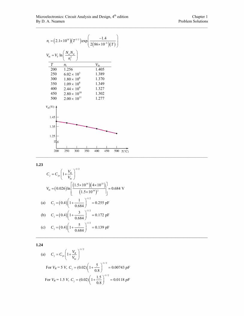
Microelectronics: Circuit Analysis and Design, 4th edition Chapter 1 By D. A. Neamen Problem Solutions ______________________________________________________________________________________
( )( ) ( )( )14 3/ 2
6
1.42.1 10 exp2 86 10in T
T−
⎛ ⎞−⎜ ⎟= ×⎜ ⎟×⎝ ⎠
2ln a dbi T
i
N NV V
n⎛ ⎞
= ⎜ ⎟⎝ ⎠
T ni Vbi200 1.256 1.405 250 6.02 × 10³ 1.389 300 1.80 × 10⁶ 1.370 350 1.09 × 10⁸ 1.349 400 2.44 × 10⁹ 1.327 450 2.80 × 10¹⁰ 1.302 500 2.00 × 10¹¹ 1.277
______________________________________________________________________________________ 1.23
1/ 2
1 Rj jo
bi
VC C
V
−⎛ ⎞
= +⎜ ⎟⎝ ⎠
( )( )( )
( )16 15
10 2
1.5 10 4 100.026 ln 0.684 V
1.5 10biV⎡ ⎤× ×⎢ ⎥= =
×⎢ ⎥⎣ ⎦
(a) ( )1/ 210.4 1 0.255 pF
0.684jC−
⎛ ⎞= + =⎜ ⎟⎝ ⎠
(b) ( )1/ 230.4 1 0.172 pF
0.684jC−
⎛ ⎞= + =⎜ ⎟⎝ ⎠
(c) ( )1/ 250.4 1 0.139 pF
0.684jC−
⎛ ⎞= + =⎜ ⎟⎝ ⎠
______________________________________________________________________________________ 1.24
(a) 1 2
1/
Rj jo
bi
VC C
V
−⎛ ⎞
= +⎜ ⎟⎝ ⎠
For VR = 5 V, 1 25(0 02) 1 0 00743
0 8
/
jC . . p.
−⎛ ⎞= + =⎜ ⎟⎝ ⎠
F
For VR = 1.5 V, 1 21 5(0 02) 1 0 0118
0 8
/
j.C . . p.
−⎛ ⎞= + =⎜ ⎟⎝ ⎠
F

Microelectronics: Circuit Analysis and Design, 4th edition Chapter 1 By D. A. Neamen Problem Solutions ______________________________________________________________________________________
0 00743 0 0118( ) 0 00962 2j
. .C avg . pF+= =
( ) ( ) ( ) ( )( ) t /C C C Cv t v final v initial v final e τ−= + −
where 3 1( ) (47 10 )(0 00962 10 )jRC RC avg .τ −= = = × × 2
or 104 52 10 . sτ −= × Then ( ) ( )1 5 0 5 0 it /
Cv t . e τ−= = + −
1 /1
5 5ln1.5 1.5
re tτ τ+ ⎛ ⎞= ⇒ = ⎜ ⎟⎝ ⎠
101 5.44 10 t s−= ×
(b) For VR = 0 V, Cj = Cjo = 0.02 pF
For VR = 3.5 V, ( )1/ 23.50.02 1 0.00863
0.8jC p−
⎛ ⎞= + =⎜ ⎟⎝ ⎠
F
0.02 0.00863( ) 0.0143 2jC avg pF+
= =
( ) 106.72 10jRC avg sτ −= = ×
( ) ( ) ( ) ( )( ) /tC C C Cv t v final v initial v final e τ−= + −
( )2 2/ /3.5 5 (0 5) 5 1t te eτ τ− −= + − = −
so that 102 8.09 10 t s−= ×
______________________________________________________________________________________ 1.25
2/1
1−
⎟⎟⎠
⎞⎜⎜⎝
⎛+=
bi
Rjoj V
VCC ; ( ) ( )( )( )
739.0105.1
10105ln026.0 210
1715
=⎥⎥⎦
⎤
⎢⎢⎣
⎡
×
×=biV V
For V, 1=RV
391.0
739.011
60.0=
+
=jC pF
For V, 3=RV
267.0
739.031
60.0=
+
=jC pF
For V, 5=RV
215.0
739.051
60.0=
+
=jC pF
(a) ( )( )
57.610391.0105.12
12
1123
=⇒××
==−−
oo fLC
fππ
MHz
(b) ( )( )
MHzff oo 95.710267.0105.12
1123
=⇒××
=−−π

Microelectronics: Circuit Analysis and Design, 4th edition Chapter 1 By D. A. Neamen Problem Solutions ______________________________________________________________________________________
(c) ( )( )
86.810215.0105.12
1123
=⇒××
=−−
oo ffπ
MHz
______________________________________________________________________________________ 1.26
a. exp 1 0.90 exp 1D DS
T T
V VI IV V
⎡ ⎤⎛ ⎞ ⎛ ⎞= − − =⎢ ⎥⎜ ⎟ ⎜ ⎟
⎝ ⎠ ⎝ ⎠⎣ ⎦−
exp 1 0.90 0.10D
T
VV
⎛ ⎞= − =⎜ ⎟
⎝ ⎠
( )ln 0.10 0.0599 VD T DV V V= ⇒ = − b.
0.2exp 1 exp 10.026
0.2exp 1exp 1 0.026
21901
2190
F
TSF
R S R
T
F
R
VVII
I I VV
II
⎡ ⎤⎛ ⎞ ⎛ ⎞−⎢ ⎥ −⎜ ⎟ ⎜ ⎟⎝ ⎠⎣ ⎦ ⎝= ⋅ =−⎡ ⎤ ⎛⎛ ⎞
⎠⎞ −− ⎜ ⎟⎢ ⎥⎜ ⎟ ⎝ ⎠⎝ ⎠⎣ ⎦
=−
=
______________________________________________________________________________________
1.27 ⎥⎥⎦
⎤
⎢⎢⎣
⎡−⎟⎟
⎠
⎞⎜⎜⎝
⎛= 1exp
T
DSD V
VII
(a) (i) ( ) μ03.1026.0
3.0exp10 11 ⇒⎟⎠⎞
⎜⎝⎛= −
DI A
(ii) ( ) 25.2026.05.0exp10 11 ⇒⎟
⎠⎞
⎜⎝⎛= −
DI mA
(iii) ( ) 93.4026.07.0exp10 11 ⇒⎟
⎠⎞
⎜⎝⎛= −
DI A
(iv) ( ) 1211 1037.51026.0
02.0exp10 −− ×−=⎥⎦
⎤⎢⎣
⎡−⎟
⎠⎞
⎜⎝⎛ −=DI A
(v) ( ) 1111 101026.0
20.0exp10 −− −≅⎥⎦
⎤⎢⎣
⎡−⎟
⎠⎞
⎜⎝⎛ −=DI A
(vi) A ( )1110−−=DI
(b) (i) ( ) μ0103.0026.0
3.0exp10 13 ⇒⎟⎠⎞
⎜⎝⎛= −
DI A
(ii) ( ) μ5.22026.05.0exp10 13 ⇒⎟
⎠⎞
⎜⎝⎛= −
DI A
(iii) ( ) 3.49026.07.0exp10 13 ⇒⎟
⎠⎞
⎜⎝⎛= −
DI mA
Microelectronics: Circuit Analysis and Design, 4th edition Chapter 1 By D. A. Neamen Problem Solutions ______________________________________________________________________________________
(iv) ( ) 1413 1037.51026.0
02.0exp10 −− ×−=⎥⎦
⎤⎢⎣
⎡−⎟
⎠⎞
⎜⎝⎛ −=DI A
(v) A 1310−−≅DI
(vi) A 1310−−≅DI______________________________________________________________________________________
1.28 ⎟⎟⎠
⎞⎜⎜⎝
⎛=
S
DTD I
IVV ln
(a) (i) ( ) 359.010
1010ln026.0 11
6
=⎟⎟⎠
⎞⎜⎜⎝
⎛ ×= −
−
DV V
( ) 419.010
10100ln026.0 11
6
=⎟⎟⎠
⎞⎜⎜⎝
⎛ ×=
−
−
DV V
( ) 479.01010ln026.0 11
3
=⎟⎟⎠
⎞⎜⎜⎝
⎛= −
−
DV V
(ii) 018.01026.0
exp10105 1112 −=⇒⎥⎦
⎤⎢⎣
⎡−⎟
⎠
⎞⎜⎝
⎛=×− −−D
D VV
V
(b) (i) ( ) 479.010
1010ln026.0 13
6
=⎟⎟⎠
⎞⎜⎜⎝
⎛ ×= −
−
DV V
( ) 539.010
10100ln026.0 13
6
=⎟⎟⎠
⎞⎜⎜⎝
⎛ ×=
−
−
DV V
( ) 599.01010ln026.0 13
3
=⎟⎟⎠
⎞⎜⎜⎝
⎛= −
−
DV V
(ii) 00274.01026.0
exp1010 1314 −=⇒⎥⎦
⎤⎢⎣
⎡−⎟
⎠
⎞⎜⎝
⎛=− −−D
D VV
V
______________________________________________________________________________________ 1.29
(a) 3 0.710 exp0.026SI− ⎛ ⎞= ⎜ ⎟
⎝ ⎠
152.03 10 ASI −= × (b)
DV ( ) ( 1)DI A n = ( )( )2DI A n =
0.1 149.50 10 −× 141.39 10 −× 0.2 124.45 10 −× 149.50 10 −× 0.3 102.08 10 −× 136.50 10 −× 0.4 99.75 10 −× 124.45 10 −× 0.5 74.56 10 −× 113.04 10 −× 0.6 52.14 10 −× 102.08 10 −× 0.7 310 − 91.42 10 −× ______________________________________________________________________________________

Microelectronics: Circuit Analysis and Design, 4th edition Chapter 1 By D. A. Neamen Problem Solutions ______________________________________________________________________________________ 1.30 (a) 1210SI A−= VD(v) ID(A) log10ID0.10 114 68 10. −× 10 3.− 0.20 92 19 10. −× 8 66.− 0.30 71 03 10. −× 6 99.− 0.40 64 80 10. −× 5 32.− 0.50 42 25 10. −× 3 65.− 0.60 21 05 10. −× 1 98.− 0.70 14 93 10. −× 0 307.− (b) 1410SI A−= VD(v) ID(A) log10ID0.10 134 68 10. −× 12 3.− 0.20 112 19 10. −× 10 66.− 0.30 91 03 10. −× 8 99.− 0.40 84 80 10. −× 7 32.− 0.50 62 25 10. −× 5 65.− 0.60 41 05 10. −× 3 98.− 0.70 34 93 10. −× 2 31.− ______________________________________________________________________________________ 1.31 a.
2 2 1
1
10 exp
ln (10) 59.9 mV 60 mV
D D D
D T
D T D
I V VI VV V V
⎛ ⎞−= = ⎜ ⎟
⎝ ⎠Δ = ⇒ Δ = ≈
b. ( )ln 100 119.7 mV 120 mVD T DV V VΔ = ⇒ Δ = ≈ ______________________________________________________________________________________ 1.32
(a) (i) ( ) 539.01022ln026.0 9 =⎟
⎠⎞
⎜⎝⎛
×=
−DV V
(ii) ( ) 599.010220ln026.0 9 =⎟
⎠⎞
⎜⎝⎛
×=
−DV V
(b) (i) ( ) 60.9026.04.0exp102 9 ⇒⎟
⎠⎞
⎜⎝⎛×= −
DI mA
(ii) ( ) 144026.065.0exp102 9 ⇒⎟
⎠⎞
⎜⎝⎛×= −
DI A
______________________________________________________________________________________
Microelectronics: Circuit Analysis and Design, 4th edition Chapter 1 By D. A. Neamen Problem Solutions ______________________________________________________________________________________ 1.33
3
14
3
12
2 10ln (0 026) ln 0 6347 V5 10
2 10(0 026) ln 0 5150 V5 10
0 5150 0 6347 V
DD t
S
D
D
IV V . .I
V . .
. V .
−
−
−
−
⎛ ⎞ ⎛ ⎞×= = =⎜ ⎟ ⎜ ⎟×⎝ ⎠⎝ ⎠
⎛ ⎞×= =⎜ ⎟×⎝ ⎠
≤ ≤
______________________________________________________________________________________ 1.34
(a) AII SS83 1046.1
026.030.0exp105.1 −− ×=⇒⎟
⎠⎞
⎜⎝⎛=×
(b) (i) ( ) 3.10026.035.0exp10462.1 8 =⇒⎟
⎠⎞
⎜⎝⎛×= −
DD II mA
(ii) ( ) 219.0026.025.0exp10462.1 8 =⇒⎟
⎠⎞
⎜⎝⎛×= −
DD II mA
______________________________________________________________________________________ 1.35
(a) ( ) 31.2026.08.0exp10 22 ⇒⎟
⎠⎞
⎜⎝⎛= −
DI nA
( ) μ05.5026.00.1exp10 22 ⇒⎟
⎠⎞
⎜⎝⎛= −
DI A
( ) 1.11026.02.1exp10 22 ⇒⎟
⎠⎞
⎜⎝⎛= −
DI mA
( ) 2322 1037.51026.0
02.0exp10 −− ×−=⎥⎦
⎤⎢⎣
⎡−⎟
⎠⎞
⎜⎝⎛ −=DI A
For V, A 20.0−=DV 2210−−=DI
For V, A 2−=DV 2210−−=DI (b)
( ) 115026.08.0exp105 24 ⇒⎟
⎠⎞
⎜⎝⎛×= −
DI pA
( ) μ253.0026.00.1exp105 24 ⇒⎟
⎠⎞
⎜⎝⎛×= −
DI A
( ) 554.0026.02.1exp105 24 ⇒⎟
⎠⎞
⎜⎝⎛×= −
DI mA
( ) 2424 1068.21026.0
02.0exp105 −− ×−=⎥⎦
⎤⎢⎣
⎡−⎟
⎠⎞
⎜⎝⎛ −×=DI A
For V, A 20.0−=DV 24105 −×−=DI
For V, A 2−=DV 24105 −×−=DI______________________________________________________________________________________

Microelectronics: Circuit Analysis and Design, 4th edition Chapter 1 By D. A. Neamen Problem Solutions ______________________________________________________________________________________ 1.36 IS doubles for every 5C increase in temperature. 1210 SI A−= at T = 300K For 120.5 10 T 295 KSI A−= × ⇒ = For 1250 10 , (2) 50 5.64n
SI A n−= × = ⇒ = Where n equals number of 5C increases. Then ( )( )5.64 5 28.2 T KΔ = =
So 295 328.2 T K≤ ≤ ______________________________________________________________________________________ 1.37
/ 5( )2 , 155 C
( 55)TS
S
I TT
IΔ= Δ =
−°
155 / 5 9(100)2 2.147 1
( 55)S
S
II
= = ×−
0
@100 C 373 K 0.03220T TV V° ⇒ ° ⇒ = @ 55 C 216 K 0.01865T TV V− ° ⇒ ° ⇒ =
( )(( )
)
9
9 8
13
3
0.6exp(100) 0.0322(2.147 10 )
0.6( 55) exp0.01865
2.147 10 1.237 10
9.374 10
(100) 2.83 10( 55)
D
D
D
D
II
II
⎛ ⎞⎜ ⎟⎝ ⎠= × ×
− ⎛ ⎞⎜ ⎟⎝ ⎠
× ×=
×
= ×−
______________________________________________________________________________________ 1.38
(a) DDPS VRIV +=
; ( ) DD VI += 6108.2 ( ) ⎟⎠
⎞⎜⎝
⎛×= −
026.0exp105 11 D
DV
I
By trial and error, V, 282.0=DV μ52.2=DI A (b) A, V 11105 −×−≅DI 8.2−=DV
______________________________________________________________________________________

Microelectronics: Circuit Analysis and Design, 4th edition Chapter 1 By D. A. Neamen Problem Solutions ______________________________________________________________________________________ 1.39
( )410 2 10D DI V= × + and ( ) 120.026 ln10
DD
IV −
⎛ ⎞= ⎜ ⎟⎝ ⎠
Trial and error. VD(v) ID(A) VD(v) 0.50 44.75 10−× 0.5194 0.517 44.7415 10−× 0.5194 0.5194 44.740 10−× 0.5194
0.5194 V
0.4740 mAD
D
V
I
=
=
______________________________________________________________________________________ 1.40 135 10 AsI −= ×
2
1 2
30(1.2) (1.2) 0.45 V80TH
RV
R R⎛ ⎞ ⎛ ⎞= = =⎜ ⎟ ⎜ ⎟+ ⎝ ⎠⎝ ⎠
0.45 , ln DD TH D D T
S
II R V V V
I⎛ ⎞
= + = ⎜ ⎟⎝ ⎠
By trial and error: 2.56 A, 0.402 VD DI Vμ= = ______________________________________________________________________________________

Microelectronics: Circuit Analysis and Design, 4th edition Chapter 1 By D. A. Neamen Problem Solutions ______________________________________________________________________________________ 1.41
(a) mA 121 == DD II
(i) ( ) 599.01010ln026.0 13
3
21 =⎟⎟⎠
⎞⎜⎜⎝
⎛==
−
−
DD VV V
(ii) ( ) 617.0105
10ln026.0 14
3
1 =⎟⎟⎠
⎞⎜⎜⎝
⎛
×=
−
−
DV V
( ) 557.0105
10ln026.0 13
3
2 =⎟⎟⎠
⎞⎜⎜⎝
⎛
×=
−
−
DV V
(b) 21 DD VV =
(i) 5.0221 === i
DDI
II mA
( ) 581.010
105.0ln026.0 13
3
21 =⎟⎟⎠
⎞⎜⎜⎝
⎛ ×== −
−
DD VV V
(ii) 10.0105105
13
14
2
1
2
1 =××
==−
−
S
S
D
D
II
II
So 21 10.0 DD II = mA 11.1 221 ==+ DDD III So mA, mA 909.02 =DI 0909.01 =DI Now
( ) 554.0105
100909.0ln026.0 14
3
1 =⎟⎟⎠
⎞⎜⎜⎝
⎛
××
=−
−
DV V
( ) 554.0105
10909.0ln026.0 13
3
2 =⎟⎟⎠
⎞⎜⎜⎝
⎛
××
= −
−
DV V
______________________________________________________________________________________ 1.42
(a) ( ) 426.2026.0635.0exp106 14
3 ⇒⎟⎠⎞
⎜⎝⎛×= −
DI mA
635.01635.0
==RI mA
mA 061.3635.0426.221 =+== DD II
( ) 641.0106
10061.3ln026.0 14
3
21 =⎟⎟⎠
⎞⎜⎜⎝
⎛
××
==−
−
DD VV V
V ( ) 917.1635.0641.02 =+=IV(b) mA 426.23 =DI
27.15.0
635.0==RI mA
mA 696.327.1426.221 =+== DD II
( ) 6459.0106
10696.3ln026.0 14
3
21 =⎟⎟⎠
⎞⎜⎜⎝
⎛
××
==−
−
DD VV V
V ( ) 927.1635.06459.02 =+=IV
Microelectronics: Circuit Analysis and Design, 4th edition Chapter 1 By D. A. Neamen Problem Solutions ______________________________________________________________________________________ ______________________________________________________________________________________ 1.43 (a) Assume diode is conducting. Then, 0.7 DV V Vγ= =
So that 20 7 23 3 30R.I . Aμ= ⇒
11 2 0 7 50
10R. .I Aμ−
= ⇒
Then 1 2 50 23 3D R RI I I .= − = − Or 26 7 DI . Aμ=
(b) Let Diode is cutoff. 1 50 R k= Ω
30 (1 2) 0 45 30 50DV .= ⋅ =
+. V
Since , 0D DV V Iγ< =
______________________________________________________________________________________ 1.44
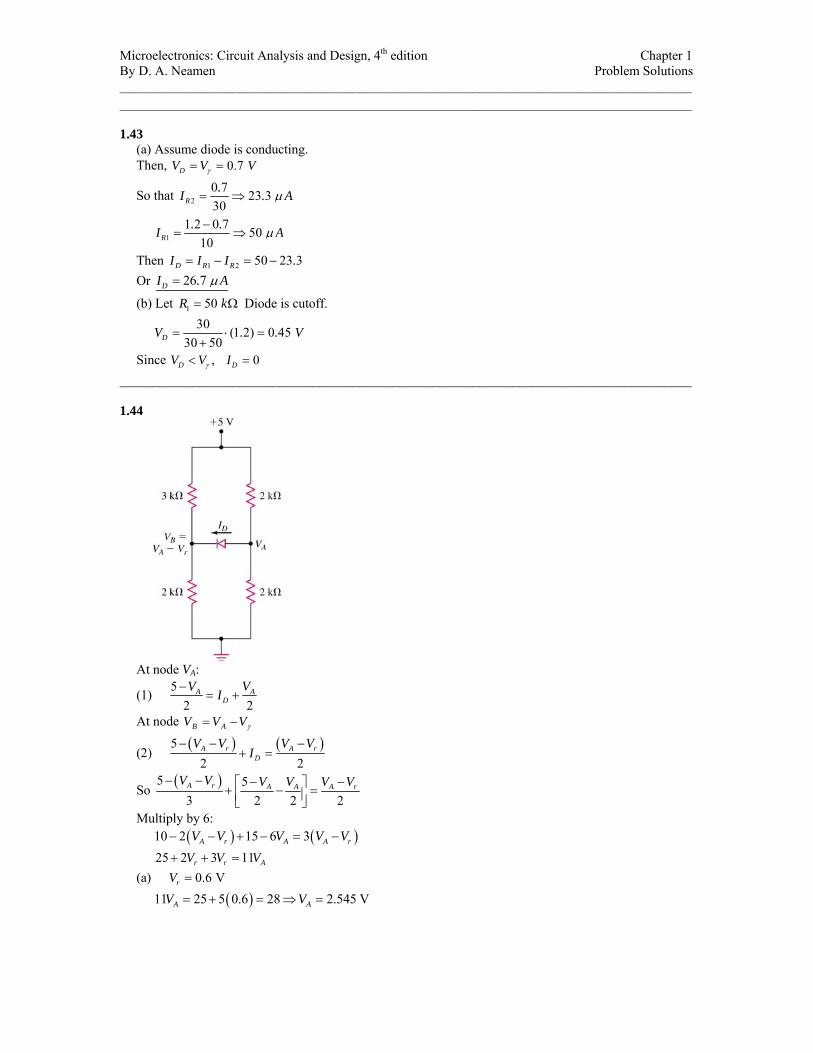
At node VA:
(1) 52 2
A AD
V VI
−= +
At node γVVV AB −=
(2) ( ) ( )52 2A r A r
D
V V V VI
− − −+ =
So ( )5 5
3 2 2A r A A AV V V V V V− − − −⎡ ⎤+ − =⎢ ⎥⎣ ⎦ 2
r
)A
Multiply by 6: ( ) (10 2 15 6 3A r A A rV V V V V− − + − = −
25 2 3 11r rV V V+ + = (a) 0.6 VrV =
( )11 25 5 0.6 28 2.545 VA AV V= + = ⇒ =
Microelectronics: Circuit Analysis and Design, 4th edition Chapter 1 By D. A. Neamen Problem Solutions ______________________________________________________________________________________
From (1) 52.5
2 2A A
D AV V
DI V I−
= − = − ⇒ Neg. 0DI⇒ =
Both (a), (b) 0DI =
VA = 2.5, 2 5 2 V 0.50 V5B DV V= ⋅ = ⇒ =
______________________________________________________________________________________ 1.45
(a) ; ; for mA ( )1iO IV = 0=DI 7.00 ≤≤ iI V; mA; for mA 7.0=OV ( 7.0−= iD II ) 7.0≥iI (b) ; ; for ( )1iO IV = 0=DI 7.10 ≤≤ iI mA V; mA; for mA 7.1=OV ( 7.1−= iD II ) 7.1≥iI (c) V; ; ; for 7.0=OV iD II =1 02 =DI 20 ≤≤ iI mA
______________________________________________________________________________________ 1.46 Minimum diode current for VPS (min) (min) 2 , 0.7 D DI mA V V= =
2 12 1
0 7 5 0 7 4 3, . .I IR R
−= = =
1
.R
We have 1 2 DI I I= +
so (1) 1 2
4 3 0 7 2. .R R
= +
Maximum diode current for VPS (max) ( )10 0 7 14 3 D D D DP I V I . I . mA= = ⇒ = 1 2 DI I I= + or
(2) 1 2
9 3 0 7 14 3. . .R R
= +
Using Eq. (1), 11 1
9 3 4 3 2 14 3 0 41 Ω. . . R . kR R
= − + ⇒ =
Then 2 82 5 82 5R . .= Ω Ω ______________________________________________________________________________________ 1.47
(a) (i) 215.020
7.05=
−=I mA, 7.0=OV V
(ii) 220.020
6.05=
−=I mA, 6.0=OV V
(b) (i) ( ) 2325.040
57.05=
−−−=I mA, ( )( ) 35.05202325.0 −=−=OV V
(iii) ( ) 235.040
56.05=
−−−=I mA, ( )( ) 30.0520235.0 −=−=OV V

Microelectronics: Circuit Analysis and Design, 4th edition Chapter 1 By D. A. Neamen Problem Solutions ______________________________________________________________________________________
(c) (i) ( ) 372.025
87.02=
−−−=I mA, ( )( ) 14.05372.02 =−=OV V
(ii) ( ) 376.025
86.02=
−−−=I mA, ( )( ) 12.05376.02 =−=OV V
(d) (i) , V 0=I 5−=OV(ii) , V 0=I 5−=OV
______________________________________________________________________________________ 1.48
(a) 20
5 OVI
−= , ( ) ⎟
⎠
⎞⎜⎝
⎛×= −
026.0exp105 14 DV
I
By trial and error, =DV 5775.0=OV V, 221.0=I mA
(b) 40
10 DVI −= , ( ) DO VIV −−= 205
mA, V, 2355.0=I 579.0=DV 289.0−=OV
(c) 25
10 DVI −= , ( )52 IVO −=
mA, V, 3763.0=I 5913.0=DV 1185.0=OV
(d) A, V 14105 −×−=I 5−≅OV______________________________________________________________________________________ 1.49 (a) Diode forward biased VD = 0.7 V 5 (0.4)(4.7) 0.7 2.42 VV V= + + ⇒ = (b) (0.4)(0.7) 0.28 mωDP I V P= ⋅ = ⇒ = ______________________________________________________________________________________ 1.50
(a) 2 1 1
2
02 1
1 1
0.65 0.65 mA1
2(0.65) 1.30 mA2 5 3(0.65) 1.30 2.35 K
R D D
D
I rD
I I I
IV V VI R
R R
= = = =
= =− − −
= = = ⇒ =
(b) 2
2 2
1 2 2
1
0.65 0.65 mA1
8 3(0.65) 3.025 mA2
3.025 0.652.375 mA
R
D D
D D R
D
I
I I
I I II
= =
−= ⇒ =
= − = −=
______________________________________________________________________________________ 1.51

Microelectronics: Circuit Analysis and Design, 4th edition Chapter 1 By D. A. Neamen Problem Solutions ______________________________________________________________________________________
a. (0 026) 0 026 k 26
1
0 05 50 A peak-to-peak
(26)(50) A 1 30 mV peak-to-peak
Td
DQ
d DQ
d d d d
V . .I
i . I
v i v .
τ
μ
τ μ
= = = Ω = Ω
= =
= = ⇒ =
b. For (0 026)0 1 mA 2600 1DQ d.I .
.τ= ⇒ = = Ω
0 05 5 A peak-to-peakd DQi . I μ= = (260)(5) V 1 30 mV peak-to-peakd d d dv i v .τ μ= = ⇒ = ______________________________________________________________________________________ 1.52
(a) 1026.0026.0
===DQ
Td I
Vr k Ω
(b) Ω⇒= 10026.0
026.0dr
(c) Ω⇒= 106.2
026.0dr
______________________________________________________________________________________ 1.53
a. diode resistance d Tr V I= /
d Td S
Td SS
Td s o
T S
r V Iv vVr R RI
Vv v vV IR
⎛ ⎞⎜ ⎟⎛ ⎞ /
= = ⎜ ⎟⎜ ⎟+⎝ ⎠ ⎜ ⎟+⎜ ⎟⎝ ⎠
⎛ ⎞= =⎜ ⎟+⎝ ⎠
Sv
b. 260SR = Ω
( ) ( )
0 0
0 0
0 0
0 0261 mA, 0 09090 026 (1)(0 26)
0 0260 1 mA, 0 500 026 0 1 0 26
0 0260 01 mA. 0 9090 026 (0 01)(0 26)
T
S T S S
s S
S S
v vV .I .v V IR . . v
v v.I . .v . . . v
v v.I . .v . . . v
⎛ ⎞= = = ⇒ =⎜ ⎟+ +⎝ ⎠
= = ⇒ =+
= = ⇒ =+
______________________________________________________________________________________

Microelectronics: Circuit Analysis and Design, 4th edition Chapter 1 By D. A. Neamen Problem Solutions ______________________________________________________________________________________ 1.54 pn junction diode
( ) 548.0105
1072.0ln026.0 13
3
=⎟⎟⎠
⎞⎜⎜⎝
⎛
××
=−
−
DV V
Schottky diode
( ) 249.0105
1072.0ln026.0 8
3
=⎟⎟⎠
⎞⎜⎜⎝
⎛
××
=−
−
DV V
______________________________________________________________________________________ 1.55
Schottky: exp aS
T
VI I
V⎛ ⎞
≅ ⎜ ⎟⎝ ⎠
3
7
0.5 10ln (0.026) ln5 10
0.1796
a TS
IV VI
V
−
−
⎛ ⎞ ⎛ ⎞×= =⎜ ⎟ ⎜ ⎟×⎝ ⎠⎝ ⎠
=
Then
of pn junction 0.1796 0.30
0.4796aV = +
=
30 5 10
0 4796exp exp 0 026
Sa
T
I .I.V.V
−×= =
⎛ ⎞ ⎛ ⎞⎜ ⎟⎜ ⎟ ⎝ ⎠⎝ ⎠
124 87 10 ASI . −= × ______________________________________________________________________________________ 1.56 (a)
Microelectronics: Circuit Analysis and Design, 4th edition Chapter 1 By D. A. Neamen Problem Solutions ______________________________________________________________________________________ 3
1 2 0 5 10I I . −+ = ×
8 125 10 exp 10 exp 0 5 10D D
T T
V V.
V V− −⎛ ⎞ ⎛ ⎞
× + =⎜ ⎟ ⎜ ⎟⎝ ⎠ ⎝ ⎠
3−×
8 35 0001 10 exp 0 5 10D
T
V. .
V− −⎛ ⎞
× =⎜ ⎟⎝ ⎠
×
3
8
0 5 10(0 026) ln 0 23955 0001 10D D
.V . V ..
−
−
⎛ ⎞×= ⇒⎜ ⎟×⎝ ⎠
=
Schottky diode, 2 0 49999 mAI .=
pn junction, 1 0 00001 mAI .= (b)
12 81 210 exp 5 10 expD D
T T
V VI
V V− −⎛ ⎞ ⎛
= = ×⎜ ⎟ ⎜⎝ ⎠ ⎝
⎞⎟⎠
1 2 0.9D DV V+ =
12 81 1
8 1
0.910 exp 5 10 exp
0.95 10 exp exp
D D
T T
D
T T
V VV V
VV V
− −
−
⎛ ⎞ ⎛ ⎞−= ×⎜ ⎟ ⎜ ⎟
⎝ ⎠ ⎝ ⎠⎛ ⎞ ⎛ −
= × ⎜ ⎟ ⎜⎝ ⎠ ⎝
⎞⎟⎠
8
112
2 5 10 0 9exp exp0 02610
D
T
V .V .
−
−
⎛ ⎞ ⎛ ⎞× ⎛ ⎞=⎜ ⎟ ⎜ ⎟ ⎜ ⎟⎝ ⎠⎝ ⎠⎝ ⎠
8
1 12
5 102 ln 0 9 1 181310D TV V . .
−
−
⎛ ⎞×= + =⎜ ⎟
⎝ ⎠
1 0 5907 pn junctionDV .=
2 0 3093 Schottky diodeDV .=
12 0 590710 exp 7 35 mA0 026.I I.
− ⎛ ⎞= ⇒ =⎜ ⎟⎝ ⎠
.
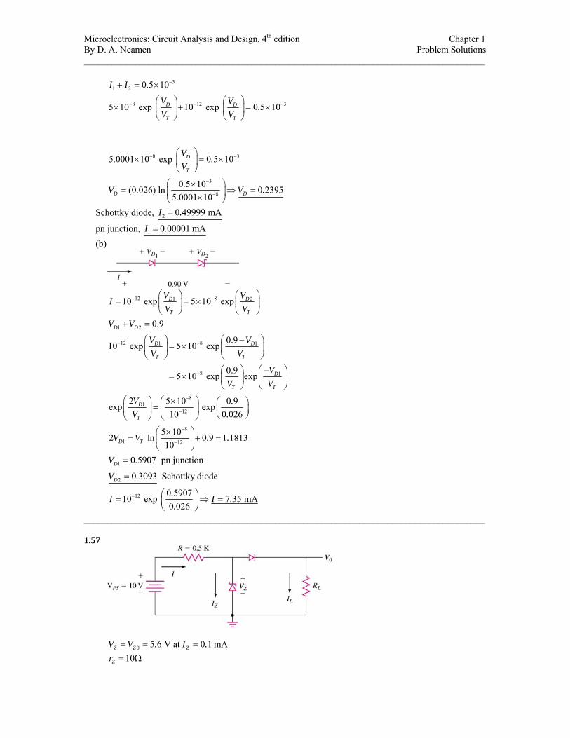
______________________________________________________________________________________ 1.57
0 5 6 V at 0 1 mAZ Z ZV V . I .= = = 10Zr = Ω
Microelectronics: Circuit Analysis and Design, 4th edition Chapter 1 By D. A. Neamen Problem Solutions ______________________________________________________________________________________ ( )( )0 1 10 1 mVZ ZI r .= = VZ0 = 5.599 a. LR →∞⇒
10 5 599 4 401 8 63 mA0 50 0 01Z
Z
. .I .R r . .−
= = =+ +
( )( )0 5.599 0.00863 10Z Z Z ZV V I r= + = + 0 5 685 VZV V .= =
b. 11 5 59911 V 10 59 mA0 51PS Z
.V I ..
−= ⇒ = =
( )( )0 5.599 0.01059 10 5.7049 VZV V= = + =
9 5 5999 V 6 669 mA0 51PS Z
.V I ..
−= ⇒ = =
( )( )0 5.599 0.006669 10 5.66569 VZV V= = + =
0 05 7049 5 66569 0 0392 VV . . V .Δ = − ⇒ Δ = c. I = IZ + IL
0 0 0, , 0PS ZL Z
L Z
V V V V VI I IR R r
− −= = =
0 010 5 5990 50 0 010 2
V V . V. .− −
= + 0
010 5 599 1 1 1
0 50 0 010 0 50 0 010 2. V
. . . .⎡ ⎤+ = + +⎢ ⎥⎣ ⎦
20.0 + 559.9 = V0 (102.5) 0 5.658 VV = ______________________________________________________________________________________ 1.58
(a) 4.65.0
8.610=
−=ZI mA
mW ( )( ) 5.438.64.6 === ZZVIP(b) mA ( )( ) 64.04.61.0 ==ZI 76.564.04.6 =−=LI mA
18.176.58.6===⇒=
Z
ZL
L
ZL I
VRRVI kΩ
______________________________________________________________________________________ 1.59 ( )( )0.1 20 2 mVZ ZI r = =
0 6 8 0 002 6 798 VZV . . .= − = a. LR = ∞
10 6 798 6 158 mA0 5 0 02Z Z
.I I .. .−
= ⇒ =+

Microelectronics: Circuit Analysis and Design, 4th edition Chapter 1 By D. A. Neamen Problem Solutions ______________________________________________________________________________________ ( )( )0 0 6.798 0.006158 20Z Z Z ZV V V I r= = + = + 0 6 921 VV .= b. Z LI I I= +
0 010 6 7980 50 0 020 1
V V . V. .− −
= + 0
010 6 798 1 1 1
0 30 0 020 0 50 0 020 1. V
. . . .⎡ ⎤+ = + +⎢ ⎥⎣ ⎦
359.9 = V0 (53) V0 = 6.791 V 0 6 791 6 921V . .Δ = − 0 0.13 VVΔ = − ______________________________________________________________________________________ 1.60 For VD = 0, 0.1 ASCI =
For ID = 0 14
0.2ln 15 10D TV V −
⎛ ⎞= +⎜ ⎟×⎝ ⎠
0.754 VD DCV V= = ______________________________________________________________________________________ 1.61 A 2.0,0 == DD IV V, A 60.0=DV 1995.0=DI V, A 65.0=DV 1964.0=DI V, A 70.0=DV 1754.0=DI V, A 72.0=DV 1468.0=DI V, A 74.0=DV 0853.0=DI V, 7545.0=DV 0=DI______________________________________________________________________________________ 1.62
(a) ( ) 7126.01026.0
exp10520.016.0 14 =⇒⎥⎦
⎤⎢⎣
⎡−⎟
⎠
⎞⎜⎝
⎛×−= −D
D VV
V
(b) W ( )( ) 114.07126.016.0 ==P______________________________________________________________________________________


