Micro- and nano-scale organic light-emitting devices ...thesis... · Micro- and nano-scale organic...
114
Micro- and nano-scale organic light-emitting devices driven by alternating-current voltage Ph.D. thesis NanoSYD Mads Clausen Institute University of Southern Denmark Supervisors: Assoc. Prof. Jakob Kjelstrup-Hansen Prof. Horst-Günter Rubahn Xuhai Liu March 15, 2013
-
Upload
nguyencong -
Category
Documents
-
view
218 -
download
0
Transcript of Micro- and nano-scale organic light-emitting devices ...thesis... · Micro- and nano-scale organic...
Micro- and nano-scale organic light-emitting devices
driven by alternating-current voltage
Ph.D. thesis
NanoSYD
Mads Clausen Institute
University of Southern Denmark
Supervisors:
Assoc. Prof. Jakob Kjelstrup-Hansen
Prof. Horst-Günter Rubahn
Xuhai Liu
March 15, 2013

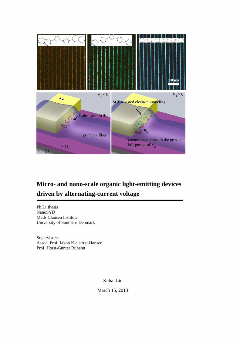
Front cover image captions
Image 1: Electroluminescence from AC-driven light-emitting transistors based on
different organic thin films.
Image 2: Schematic illustration of the operating mechanism of AC-driven light-
emitting transistors based on organic nanofibers.
3
Curriculum vitae
Xuhai Liu was born in 1985 in Qingdao, China. In 2007, he received a Bachelor of
Science degree in Mechanical Design and Automation from Northwestern
Polytechnical University in Xi’an, China. Afterwards, he came to Denmark to study
Embedded Software and one year later shifted his research interest to
nanotechnology. In 2009, he received a Master of Science in Engineering degree in
Mechatronics from University of Southern Denmark, Sønderborg. He then pursued
his doctorate degree in Functional Materials and Nanotechnology in the same
research group under the supervision of Assoc. Prof. Jakob Kjelstrup-Hansen and
Prof. Horst-Günter Rubahn. His research interests include organic light-emitting
devices in a transistor configuration and charge transport properties of organic
materials.

4
5
Preface
This Ph.D. thesis regarding organic light-emitting devices is based on my theoretical
study and experimental research carried out from March 15th, 2010 to March 15
th,
2013 at NanoSYD at the Mads Clausen Institute, University of Southern Denmark.
During the project period I mainly worked on light-emitting devices based on organic
thin films and nanofibers, and also contributed in other experimental investigations
with colleagues in our group and visiting international researchers. A number of
publications have been made during this project and they are listed in Appendix A.
Apart from the research project, I also took part in other academic activities. Firstly, I
succeeded in all the mandatory courses covering 30 ECTS, including two individual
courses about microfabrication and computational chemistry. This provided me with
solid theoretical background and a better vision of my experimental plan and
outcome. Secondly, I contributed in building a probe station for electrical
characterization of semiconductor devices, and a vacuum chamber system for
thermal evaporation of organic materials. This improved my experimental skills and
allowed me to better understand the experimental tools and facilities. Thirdly, I
participated in four nanotechnology related conferences and gave one oral
presentation and three poster presentations, which provided me with an excellent
platform to meet talented researchers from around the world and improve my
academic communicating skills. Next, I had two pleasant research stay in Institute of
Electrical and Information Engineering of Christian-Albrechts-University of Kiel,
and National Center for Nanoscience and Technology (NCNST) of the Chinese
Academy of Sciences. During the visiting period, I experienced different research
habits and surroundings and it strengthened my capability to quickly adapt to new
academic environment. Last but not least, I delivered lectures regarding Elasticity
and COMSOL simulation to Master students.
I sincerely hope that this thesis will be helpful for the readers.
Xuhai Liu
NanoSYD, Mads Clausen Institute
University of Southern Denmark
Alsion 2, 6400 Sønderborg, Denmark
March, 2013

6
7
Acknowledgements
First and foremost, I would like to thank my project supervisor Prof. Jakob Kjelstrup-
Hansen. I have been studying and working under his supervision for four years in
terms of experimental work and theoretical discussion, as well as the preparation of
manuscripts for journals. I would not grow into the scientist I am today without him.
His example of being sincere, diligent, persistent, meticulous in scientific details has
inspired me a great deal. I would also like to thank my main supervisor Horst-Günter
Rubahn for helpful and critical discussion and guidance in many aspects of my Ph. D.
work. His great personality and academic success will always inspire me to pursue a
successful career. Also special thanks should go for the visiting professor, Henri
Boudinov, from UFRGS Brazil. It was a pleasant experience to work with him for
several months.
I am grateful to other collaborators of journal and conference articles. Dr. Henrik
Hartmann Henrichsen helped me a lot with initial experimental setup. Dr. Ivonne
Wallmann, Andreas Osadnik and Prof. Arne Lützen from University of Bonn
together with our previous group member Dr. Manuela Schiek synthesized and
provided important organic materials which are essential to the semiconductor
devices in my work. Prof. Jacob Kongsted from Department of Physics, Chemistry
and Pharmacy of University of Southern Denmark taught me computational
chemistry and helped me in great details regarding the output analysis of Gaussian
calculations. Dr. Roana Melina de Oliveira Hansen initially taught me electron beam
lithography, and she also assisted me in many aspects of my experimental work. I
would also like to thank Mr. Fei Liu, who is currently a Ph.D. student in University
of Twente, for his important work on self-assembled monolayer modified organic
devices. Many thanks are also due to Mr. Henrik Høyer and Prof. Matti Knaapila
from NTNU Norway for the pleasant cleanroom work.
I am also very grateful to Prof. Martina Gerken for allowing me to stay in her
research group in Christian-Albrechts-University of Kiel for a short visit. It was my
great pleasure to work with her Ph.D. student Christian Kluge on experimental setup
and optical measurements. Also, I would like to thank Prof. Chao Jiang from Chinese
Academy of Sciences in Beijing for offering me a short visit to his group. A lot of
gratitude is due to his colleagues and students, such as Dr. Dexing Li, Nan Ai, and
Mr. Yiwei Zhang, Jieze Wang, and Miss Misbah Mirza.
I would like to acknowledge other colleagues in our group for their direct and
indirect help. In particular, I wish to thank the technician team, Dr. Kasper Thilsing-
Hansen, Mogens Melskens Petersen, and Reiner Hübel for their excellent

8
maintenance of all the experimental equipment in different laboratories. Also kind
thanks are due to our group secretary Ms. Zora Milde for her administrative help.
Finally, I would like to thank my family for their unconditional support and
encouragement.
9
Abstract
Organic optoelectronics has experienced significant development and success both in
research and on the market level during the past decade. The concept of optical-to-
electrical or electrical-to-optical energy conversion, together with property tunability
of organic materials via chemical synthesis as well as advanced micro- and nano-
scale fabrication processes on various substrates, enable a great number of novel
applications in our daily life. For instance, organic light-emitting diodes (OLEDs)
have been widely used in portable consumer electronics and large flat panel displays.
Also, the integration of light sources such as OLEDs, and light detectors such as
organic phototransistors (OPTs), can enable novel lab-on-a-chip system for medical
diagnosis.
The main purpose of this thesis is to describe the result of investigations on novel
organic light-emitting devices driven by alternating-current (AC) gate voltage on a
transistor platform, as well as to present light detectors based on organic crystals in
the same transistor configuration, so as to illustrate the possibility to integrate
organic light sources and detectors in micro- and nano-scale devices.
Organic small molecule-based thin films were mainly used as the active materials to
study the charge carrier injection, transport and light generation mechanism on a
micro-scale transistor platform operated by AC gate voltage. Combining time-
resolved experiments, low-temperature investigations as well as corresponding
calculations, an operating model mainly involving space-charge field assisted charge
carrier injection was proposed. This operating mechanism was subsequently
implemented in more crystalline organic nanofiber-based nano-scale transistor
platform, and corresponding electroluminescence from these nano-scale devices were
obtained.
Density functional theory (DFT) calculations have been carried out to estimate the
device properties related to charge transport and photon absorption. Micro-scale
OPTs based on organic nanofibers and thin films have been fabricated and
subsequently characterized in darkness and under illumination. The obvious superior
photoresponsivity of the nanofiber-based OPTs compared with thin film OPTs
demonstrates that nanofibers have great potential for high-performance
photosensitive devices, mainly attributed to the highly ordered molecular packing in
the crystalline structures.

10
11
Dansk resumé
Organisk optoelektronik har oplevet en betydelig udvikling og succes både i
forskningsverdenen og på markedsniveau i løbet af det seneste årti. Konceptet om
optisk-til-elektrisk eller elektrisk-til-optisk energi konvertering kombineret med
muligheden for at tilpasse egenskaberne af organiske materialer ved kemisk syntese
samt avancerede mikro-og nano-skala fremstillingsprocesser på forskellige substrater
muliggør et stort antal nye applikationer i vores daglige liv. For eksempel har
organiske lysdioder (OLED) været meget anvendt i bærbar forbrugerelektronik og
store fladskærme. Desuden kan integration af lyskilder såsom OLED’er og
lysdetektorer såsom organiske fototransistorer (OPT) muliggøre nye lab-on-a-chip
systemer til medicinsk diagnose.
Hovedformålet med denne afhandling er at beskrive resultatet af undersøgelser af
nye organiske lys-udsenende komponenter drevet af vekselspænding (AC) på gate-
kontakten af en transistor platform, samt at præsentere lysdetektorer baserede på
organiske krystaller i en lignende transistor-konfiguration for at illustrere muligheden
for at integrere organiske lyskilder og -detektorer i mikro-og nano-skala enheder.
Organiske tyndfilm baserede på små molekyler blev hovedsagelig benyttet som det
aktive materiale til at undersøge ladningsbærer-injektion og -transport og
mekanismen hvorved lys bliver genereret på en mikroskala transistor platform drevet
af en AC gatespænding. Ved at kombinere tidsopløste eksperimenter, lav-temperatur
undersøgelser samt tilsvarende beregninger blev en model udviklet, som
hovedsageligt involverer et rumladningsfelt som bidrager til ladningsbærerinjektion.
Den virkningsmåde blev efterfølgende implementeret i mere krystallinske, organisk
nanofiber-baserede, nano-skala transistorer, og tilsvarende elektroluminescens fra
disse nano-skala komponenter blev opnået.
Density Functional Theory (DFT) beregninger er blevet udført for at vurdere
komponentens egenskaber relateret til at ladningstransport og foton-absorption.
Mikro-skala OPT’er baseret på organiske nanofibre og tyndfilm er blevet fremstillet
og efterfølgende karakteriseret både i mørke og under belysning. Den væsentligt
højere fotoresponsivitet af de nanofiber-baserede OPT’er sammenlignet med
tyndfilm OPT’er viser, at nanofibrene har et stort potentiale som højtydende
lysfølsomme komponenter, hvilket primært tilskrives den meget ordnede molekylære
pakning i de krystallinske strukturer.

12
13
Contents
Abbreviations ............................................................................................................. 15
Chapter 1: Introduction .............................................................................................. 17
1.1 Devices ............................................................................................................. 18
1.1.1 Organic light-emitting diodes (OLEDs) .................................................... 18
1.1.2 Organic light-emitting transistors (OLETs) .............................................. 20
1.1.3 Organic phototransistors (OPTs) ............................................................... 23
1.2 Materials ........................................................................................................... 24
1.2.1 Molecules .................................................................................................. 24
1.2.2 Morphology: thin films and nanofibers ..................................................... 26
1.3 Materials and devices used in this project ........................................................ 27
1.4 Structure of the thesis ....................................................................................... 28
Chapter 2: Charge injection and transport .................................................................. 31
2.1 Theory .............................................................................................................. 31
2.1.1 Energy levels ............................................................................................. 31
2.1.2 Theoretical approaches to charge injection ............................................... 33
2.1.3 Introduction of density functional theory (DFT) and basis sets ................ 35
2.1.4 Intrinsic charge transport ........................................................................... 36
2.2 Calculations ...................................................................................................... 39
2.2.1 Energy levels ............................................................................................. 39
2.2.2 Transfer integral ........................................................................................ 40
2.2.3 Reorganization energy............................................................................... 42
2.2.4 Intrinsic mobility ....................................................................................... 44
2.3 Chapter summary ............................................................................................. 45
Chapter 3: OLETs based on thin films and transferred nanofibers ............................ 47
3.1 Photoluminescence (PL) of organic thin films ................................................. 47
3.2 Operating mechanism ....................................................................................... 48
3.2.1 Preparation of micro-scale transistors ....................................................... 48
14
3.2.2 Electrical characteristics ........................................................................... 49
3.2.3 Electroluminescence (EL) from p6P thin films and operating mechanism
........................................................................................................................... 51
3.2.4 Self-assembled monolayer (SAM) modification ...................................... 59
3.3 OLETs based on PPTPP, NaT and NaT2 thin films ........................................ 61
3.4 OLETs based on transferred p6P nanofibers ................................................... 64
3.4.1 Growth of nanofibers and transfer ............................................................ 65
3.4.1 Low-temperature study of transferred nanofibers ..................................... 65
3.4.2 Electroluminescence from transferred nanofibers .................................... 66
3.5 Chapter summary ............................................................................................. 67
Chapter 4: Nano-scale OLETs ................................................................................... 69
4.1 Preparation of nano-scale transistors ............................................................... 69
4.2 Electroluminescence from in-situ grown nanofibers ....................................... 71
4.3 Chapter summary ............................................................................................. 74
Chapter 5: OPTs based on thin films and nanofibers ................................................ 75
5.1 Experimental .................................................................................................... 75
5.2 Chapter summary ............................................................................................. 82
Chapter 6: Conclusions and outlook .......................................................................... 83
Appendices ................................................................................................................ 85
A: List of publications ........................................................................................... 85
B: Derivations of drain-source current .................................................................. 87
C: HOMO and LUMO orbitals .............................................................................. 91
D: Micro-scale device fabrication recipe ............................................................... 93
E: Extraction of emission intensity of p6P thin film based OLET ........................ 95
Bibliography .............................................................................................................. 99
15
Abbreviations
6T Sexithiophene
AC voltage Alternating-Current voltage
ADF Amsterdam density functional
AFM Atomic force microscope
Alq3 Tris(8-hydroxyquinolinato) aluminum
BC/BG Bottom Contact/Bottom Gate
BC/TG Bottom Contact/Top Gate
BPE N,N -bis(2-phenylethyl)-perylene-3,4:9,10-tetracarboxylic
diimide
CCDs Charge-coupled devices
CI Configuration interaction
CMOS Complementary metal-oxide semiconductor
DC voltage Direct-Current voltage
DFT Density functional theory
DZP Double zeta polarization
EBL Electron beam lithography
EL Electroluminescence
EML Light emitting layer
EQE External quantum efficiency
F-N Fowler-Nordheim
HIL Hole injection layer
HOMO Highest Occupied Molecule Orbital
HTL Hole transport layer
ITO Indium tin oxide
KCL Potassium chloride
LUMO Lowest Unoccupied Molecule Orbital
MP2 Second-order Møller-Plesset
16
NaT 2,5-bis(naphthyl)-thiophene
NaT2 5,5-bis(naphthyl)-2,2′-bithiophene
NaT3 5,5’’-bis(naphtha-2-yl)-2,2’:5’,2’’-terthiophene
ODT Octadecanethiol
OFET Organic field-effect transistor
OLED Organic light-emitting diode
OLET Organic light-emitting transistor
OPT Organic phototransistor
OTS Octadecylchlorosilane
P3HT Poly-3-hexylthiophene
p6P Para-hexaphenylene
PFDT 1H,1H,2H,2H-Perfluorodecanethiol
PL Photoluminescence
PMMA Poly(methyl methacrylate)
PMT Photomultiplier tube
PPTPP 2,5-bis (4-biphenylyl) thiophene
PPTTPP 5,5’-di-4-biphenylyl-2-2’-bithiophene
PPV Poly(p-phenylene vinylene)
PTCDI-C8 N,N -dioctyl-3,4,9,10-perylene tetracarboxylic diimide
RT Room temperature
SAMs Self-assembled monolayers
SCF Space-charge field
SEM Scanning electron microscope
TC/BG Top Contact/Bottom Gate
TTPPTT 4,4’-di-2,2’-bithienylbiphenyl
UV Ultraviolet
17
Chapter 1: Introduction
Optoelectronics, which is the study of the electronic devices that source and detect
light, constitutes a vibrant research field due to its wide applications and its huge
potential to lead to novel devices. The past decades have witnessed a great number of
fully commercialized optoelectronic products, which include light-emitting diodes
(LEDs) for lighting and as display components, photodiodes as detectors,
photovoltaic cells as a renewable energy technology, photomultiplier tubes (PMTs)
as ultra-sensitive detectors, charge-coupled devices (CCDs) for imaging, high power
laser diodes for industrial machining and so on. Intensive investigations on
optoelectronics are continuing, particularly in an attempt for minimization into
micro- and nano-scale for more power efficient devices [1-4].
The above mentioned optoelectronic devices are all typically based on inorganic
semiconductors, e.g. silicon, germanium, gallium arsenide, etc. In inorganic
semiconductors, electrons can be excited from the valence band (formed due to
valence electrons bound to atoms) onto the conduction band (formed due to
conduction electrons, which can move freely among the atomic lattice) via external
stimuli, and these electrons subsequently become free moving charge carriers. The
vacancies in the valence band are treated also as free mobile charge carriers, namely
holes. The resulting electrons and holes can move as highly delocalized waves, and
with mean free paths on the order of three magnitudes higher compared with the
lattice constant of the inorganic semiconductor, which can result in charge carrier
mobility as high as ~103 cm
2V
-1s
-1 [5].
The high charge carrier mobility of inorganic semiconductors is the vital factor to lay
the foundation of modern computing era, which requires higher processing speed in
complementary metal-oxide semiconductor (CMOS) logic. However, such high
charge carrier mobility is not crucial to many optoelectronic applications. For
instance, thin-film amorphous silicon (a-Si), which is widely used in current display
applications, only possesses a carrier mobility of ~1 cm2V
-1s
-1 [6]. On the other hand,
the inorganic semiconductor-based optoelectronic devices generally require complex
processing and fabrication techniques, which result in high product cost, especially in
large-area applications [7-8].
Organic semiconductors, which have been improved to have comparable carrier
mobility to a-Si, have attracted great research attention due to their potential for more
efficient, large-area, low-cost, light weight, and mechanical flexible optoelectronic
18
devices [9-14]. The organic materials can be roughly classified into small molecules
which are mainly deposited by vacuum evaporation [15-16], and semiconducting
polymers which are usually solution processed [17-18].
In the consumer market view, organic light-emitting sources, such as OLEDs, have
been implemented in various prototypes and commercialized large-area display
applications. For instance, Kodak and Sanyo introduced the prototype of a full color
display based on white OLED with integrated color filters in 2002. Epson produced a
40 inch OLED display in 2004, demonstrating a serious candidate to replace
conventional large-area displays. Sony introduced the world’s first OLED television,
11 inch XEL-1, in 2007. Both Samsung and LG showcased their 55 inch super
OLED television with full 3D support in 2012. In the small display market, various
displays based on less expensive passive-matrix OLED have been integrated into
watch, cell phone, walkman, MP3 player, etc. The consumer market can also
envisage novel applications, such as ‘electronic paper’ which integrates flexible and
even stretchable optoelectronics [19-21], and bio-compatible devices which can be
implemented in the medical field [22-23].
Investigations on organic optoelectronics are continuing to further optimize the
device structure and system configuration, to increase the power efficiency, and to
explore the integration possibility of different optoelectronic devices. This thesis
focuses on the AC-driven OLETs, as well as nanofiber-based OPTs. They act as light
sources and detectors, respectively, and they have great potential to be integrated into
novel lab-on-a-chip system [24-25]. Since the operating mechanism of OLETs in this
project can be regarded as the mixture of OLED and conventional direct-current (DC)
voltage-driven OLET, the background information of all these devices are provided
in the following introduction. The active organic materials are also elaborated in this
section. In this work, we focus on the organic materials based on small molecules.
The morphology of the small molecule-based materials can be divided into
amorphous-like thin films [26-28] and crystalline nanofibers [29-31].
1.1 Devices
1.1.1 Organic light-emitting diodes (OLEDs)
This thesis focuses on AC-driven light-emitting transistors, and interestingly, the first
investigations on electroluminescence from organic materials were also driven by
AC voltage in a diode configuration. In 1950s, Bernanose et al. firstly obtained
electroluminescence from thin films of acridine orange and quinacrine, which was
driven by a high AC field [32-34]. Later in 1963, Pope et.al utilized DC voltage as
high as 400 V as well as AC voltage and observed electroluminescence from a thin
layer of single crystal anthracene [35]. The requirement of high electric field could
be due to unsuitable electrodes used, e.g. silver paste electrode and simple electrolyte
19
electrode, and the inserted dielectric layer could also be responsible for the strict
operating conditions. These first investigations on organic electroluminescence did
not draw much research attention, and industrial interests were also lacking due to
the high voltage requirement.
The critical breakthrough showing practical importance of OLED was achieved by
Tang et al. in 1987 [36]. They initiated the utilization of a transparent hole injection
electrode of indium tin oxide (ITO), which was aimed to improve the extraction
efficiency of electroluminescence, and the electron injection electrode of
magnesium:silver (Mg:Ag) was employed to facilitate the injection of electrons.
They also firstly utilized a vapor deposited double layer of small molecule materials
sandwiched between the metal electrodes, i.e. aromatic diamine as the hole
transporting layer and tris(8-hydroxyquinolinato) aluminum (Alq3) as the electron
transporting layer. The properly chosen electrodes and organic materials together
with a suitable device configuration enabled an external quantum efficiency of 1%,
luminous efficiency of 1.5 lm W-1
, and brightness larger than 1000 cd m-2
at a driving
voltage of below 10 V. This landmark work paved the way for the currently
commercialized OLED displays, which are mostly based on small-molecule organic
materials.
Instead of small-molecule materials, Burroughes et al. implemented the conjugated
polymer poly(p-phenylene vinylene) (PPV) as the single active organic layer
sandwiched between metal electrodes of bottom indium oxide and top aluminum (Al)
in early 1990 [37]. They demonstrated that large-area organic light-emitting displays
could be fabricated using the easily prepared solution-processed polymer. This work
on polymer OLED was followed immediately by Braun et al. using a soluble
derivative of PPV [38-40]. Based on these initial investigations on polymer OLEDs,
novel television display fabricated by polymer-printing techniques are nowadays on
the verge of becoming fully commercialized [41-42].
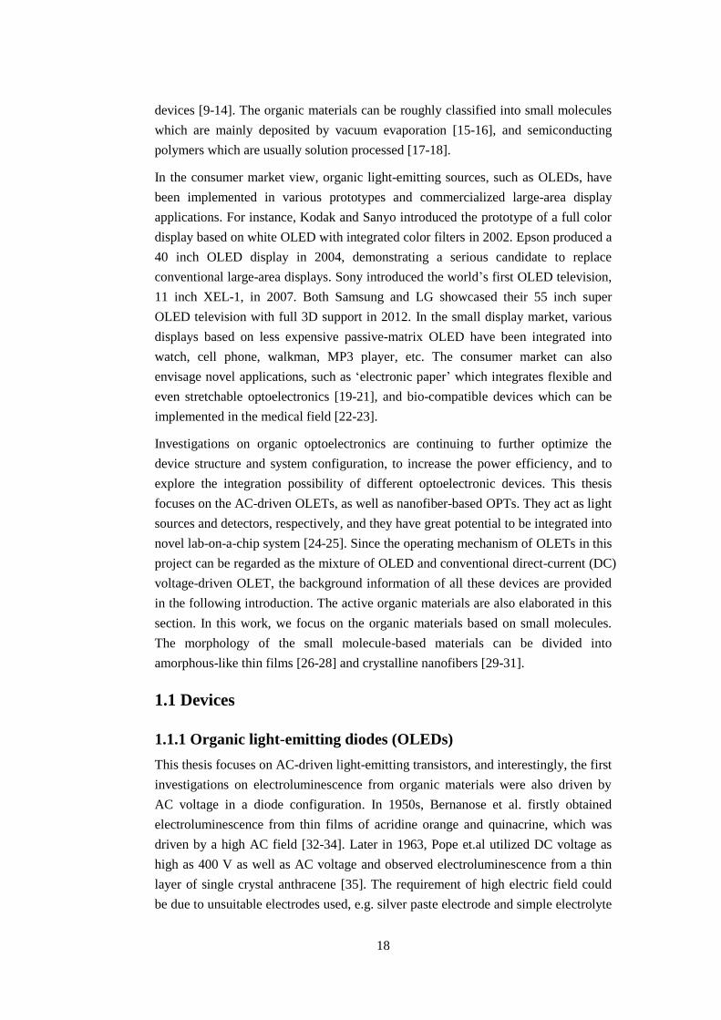
The standard OLED structure, both for small-molecule and polymer based devices,
consists of the organic material sandwiched between two electrodes with different
work functions. Take the polymer OLED for instance, the basic device configuration
is illustrated in Figure 1.1. Based on the outcoupling direction of the light, the device
configuration can be classified as the bottom emission device (a) and the top
emission device (b). In the bottom emission configuration for example, a hole
injection layer (HIL) is deposited onto the anode ITO with glass as the substrate. A
hole transport layer (HTL) is made on top of the HIL layer, and over the HTL layer is
applied the light emitting layer (EML), which also acts as the electron transport layer.
A cathode with a low work function is finally prepared on top to provide the electron
injection. The easily fabricated bottom emission device normally possess a smaller
20
external quantum efficiency ηext as a component in a display system, compared with
the top emission device [43].
Figure 1.1: Device configuration of a polymer OLED. (a) Bottom-surface emission design. (b) Top-
surface emission design. Reproduced from [43].
The external quantum efficiency (EQE) of an OLED can be described by [44]:
ext st PL outcR Eq. (1.1)
where Rst is the singlet to triplet ratio, γ is the charge balance factor, ΦPL is the
intrinsic quantum efficiency of radiative decay, Φoutc is the outcoupling efficiency.
For fluorescent materials, Rst is normally 0.25, because the injection holes and
electrons recombine to form singlet to triplet excitons in a ratio of 1:3 and only the
singlet excitons can yield fluorescence [45]. Unlike fluorescent materials,
phosphorescent materials can make use of both singlet and triplet excited states,
which means that the value of Rst is not necessary to be considered for
phosphorescence [44,46]. Recently, a method for promoting spin up-conversion from
triplet states to singlet states was proposed by Adachi et al., and this novel technique
involving delayed fluorescence has great potential to break the conventional limit of
internal quantum efficiency of fluorescent materials [47-49].
1.1.2 Organic light-emitting transistors (OLETs)
Organic field-effect transistors (OFETs) are usually used as the driving circuit
components for OLEDs in the organic active matrix display technology [50-51]. The
integration of OFETs normally leads to higher complexity of the components and
circuitry. Therefore, OLETs, which combine the electrical switching functionality of
OFETs and the light-emitting capability, could simplify the circuit design of an
active matrix display system [52-53]. Intensive investigations have been carried out
since the report of the first OLET in 2003 [54], and OLETs have recently been
shown to outperform OLEDs in terms of efficiency and brightness, mainly because
the exciton-charge annihilation and electrode photon losses can be prevented in the
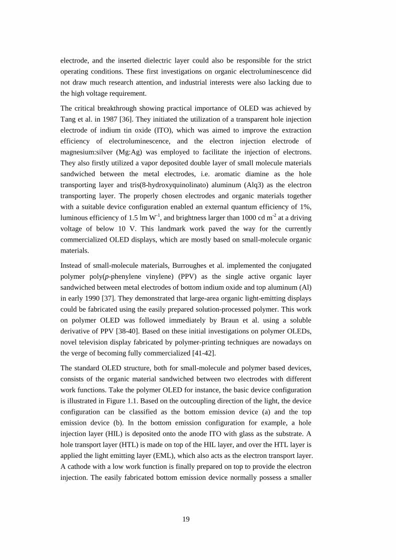
21
planar transistor configuration illustrated in Figure 1.2 [55]. These advantages of
OLETs render them as the potential new components for the next generation of
displays.
Figure 1.2: Schematic illustration of an OLET in a side view (a) and a top view (b). Reproduced from
[52].
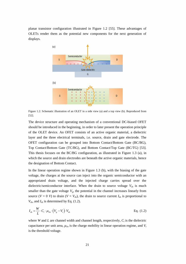
The device structure and operating mechanism of a conventional DC-biased OFET
should be introduced in the beginning, in order to later present the operation principle
of the OLET device. An OFET consists of an active organic material, a dielectric
layer and the three electrical terminals, i.e. source, drain and gate electrode. The
OFET configuration can be grouped into Bottom Contact/Bottom Gate (BC/BG),
Top Contact/Bottom Gate (TC/BG), and Bottom Contact/Top Gate (BC/TG) [53].
This thesis focuses on the BC/BG configuration, as illustrated in Figure 1.3 (a), in
which the source and drain electrodes are beneath the active organic materials, hence
the designation of Bottom Contact.
In the linear operation regime shown in Figure 1.3 (b), with the biasing of the gate
voltage, the charges at the source can inject into the organic semiconductor with an
appropriated drain voltage, and the injected charge carries spread over the
dielectric/semiconductor interface. When the drain to source voltage Vds is much
smaller than the gate voltage Vg, the potential in the channel increases linearly from
source (V = 0 V) to drain (V = Vds), the drain to source current Ids is proportional to
Vds, and Ids is determined by Eq. (1.2).
ds i lin g t ds
WI C V V V
L Eq. (1.2)
where W and L are channel width and channel length, respectively, Ci is the dielectric
capacitance per unit area, µlin is the charge mobility in linear operation regime, and Vt
is the threshold voltage.
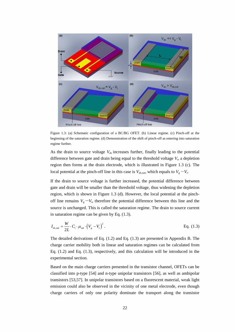
22
Figure 1.3: (a) Schematic configuration of a BC/BG OFET. (b) Linear regime. (c) Pinch-off at the
beginning of the saturation regime. (d) Demonstration of the shift of pinch-off as entering into saturation
regime further.
As the drain to source voltage Vds increases further, finally leading to the potential
difference between gate and drain being equal to the threshold voltage Vt, a depletion
region then forms at the drain electrode, which is illustrated in Figure 1.3 (c). The
local potential at the pinch-off line in this case is Vds,sat, which equals to Vg-Vt.
If the drain to source voltage is further increased, the potential difference between
gate and drain will be smaller than the threshold voltage, thus widening the depletion
region, which is shown in Figure 1.3 (d). However, the local potential at the pinch-
off line remains Vg-Vt, therefore the potential difference between this line and the
source is unchanged. This is called the saturation regime. The drain to source current
in saturation regime can be given by Eq. (1.3).
2
,2
ds sat i sat g t
WI C V V
L . Eq. (1.3)
The detailed derivations of Eq. (1.2) and Eq. (1.3) are presented in Appendix B. The
charge carrier mobility both in linear and saturation regimes can be calculated from
Eq. (1.2) and Eq. (1.3), respectively, and this calculation will be introduced in the
experimental section.
Based on the main charge carriers presented in the transistor channel, OFETs can be
classified into p-type [54] and n-type unipolar transistors [56], as well as ambipolar
transistors [53,57]. In unipolar transistors based on a fluorescent material, weak light
emission could also be observed in the vicinity of one metal electrode, even though
charge carriers of only one polarity dominate the transport along the transistor
23
channel [54]. This is because charge carriers of another polarity can tunnel through
the high injection barrier and contribute to the radiative recombination. However, the
output light is normally extremely weak due to the unbalanced charge carrier
injection and exciton quenching at the metal electrode. In contrast, the light emission
from ambipolar transistors, characterized by the comparable injection and transport
of holes and electrons, can be optimized by varying the DC biasing voltage and be
obtained in the center of the transistor channel, thus having balanced charge carrier
recombination and negligible exciton quenching [53,58].
A novel biasing approach of OLET involving AC gate voltage was demonstrated by
Yamao et al., which facilitated clear light emission both from amorphous films and
single crystals [59-61]. In their work, the electroluminescence (EL) of the organic
materials is assumed to be due to the recombination of holes and electrons injected
from the source and drain electrode, respectively, during different half-periods of the
AC gate voltage. However, the low resolution of the optical image of the
electroluminescence they provided cannot well demonstrate and support their
argument that an emission line between metal electrodes should exist due to
recombination of the charge carriers injected from separate electrodes.
In contrast, we have demonstrated AC-driven light emission from a BC/BG OLET
platform and observed light emission near an individual electrode as well as from
both sides of the transistor channel. We revealed a device operating mechanism that
combines hole injection and space-charge field (SCF) assisted electron tunneling
from an individual metal electrode. Our proposed device operating mechanism can
explain well the light emission from a unipolar transistor platform driven by AC gate
voltage [62-65]. Similar electroluminescence from AC biased OLET was also
reported by Ohtsuka et al. using a BC/TG transistor platform [66]. The detailed
investigation is documented in the experimental section, and more discussion on the
operation mechanism of AC-driven OLET will be presented later.
1.1.3 Organic phototransistors (OPTs)
In OPTs, in addition to the three terminals of a transistor platform, an external light
source can be used as the fourth terminal in OPTs to control the density of photo
carriers in the transistor channel, thus integrating electrical switching and light
detection into an individual optoelectronic device. The possibility of realizing high
sensitivity and low noise photoconductive systems render OPTs as an intensive
research target, and various active organic semiconductors and metal/dielectric
combinations have been investigated [67-71].
Various factors determine the performance of OPTs, such as the photoresponsivity,
the spectrum response, etc. The photoresponsivity is usually denoted as R, and it can
be defined as [67]
24
, ,ds illum ds dark
inc
I IR
A P
Eq. (1.4)
where Ids,illum and Ids,dark are the drain-source current under illumination and in
darkness, respectively, and A is the effective device area; Pinc is the intensity of the
incident light. The photoresponsivity determines whether the OPT is an efficient
photodetector, which means that a higher value of the photoresponsivity suggests
better functionality of the OPT even under a weak illumination. The spectrum
response is mainly determined by the intrinsic property of the active organic
semiconductor. For instance, OPTs based on materials with small energy gap are
only suitable for detecting visible light or infrared light, whereas OPTs based on
materials with large energy gap may be also utilized to detect ultraviolet (UV) light.
The energy gap will be introduced in the theoretical section later.
The performance of OPTs has been improved significantly. The highest responsivity
reported until today observed by Cho et al. was 4300 AW-1
under illumination with a
light intensity of 7 µW cm-2
by using soluble star-shaped oligothiophenes with four-
armed π-conjugation paths [72]. Kim et al. reported that the current on-off ratio of a
6,13-bis(pentylphenylethynyl) pentacene-based OPT can be up to 107 [73]. However,
only few studies in the literature have demonstrated OPTs made of organic
crystalline structures [74-75], and particularly, the direct comparison of crystalline
materials to amorphous-like thin film-based OPTs is rare [76-77]. Mukherjee et al.
obtained 40 times higher photoresponsivity from n-type phototransistors based on
solution grown ordered N,N -dioctyl-3,4,9,10-perylene tetracarboxylic diimide
(PTCDI-C8) nanowires compared with thin film-based OPTs of the same material
[76]. Yu et al. observed that N,N -bis(2-phenylethyl)-perylene-3,4:9,10-
tetracarboxylic diimide (BPE-PTCDI) nanowire-based n-type OPTs exhibit more
than 103 times larger photoresponsivity than that of thin film OPTs at a gate voltage
of 50 V [77].
1.2 Materials
1.2.1 Molecules
In this thesis, we focus on small molecules-based organic materials. Among the vast
variety of organic semiconductor based on small molecules, acene, phenylene and
thiophene oligomers along with their derivatives have been intensively investigated
[78-81]. In particular, pentacene is considered to be the organic material with the
most outstanding transport properties both for crystalline and amorphous
configurations [82-83]. Moreover, thiophene-phenylene co-oligomers [84] and
naphthyl end-capped thiophenes [85] are also appealing materials to be applied in
optoelectronic devices due to their various intermolecular packing and the ability to
self-assembled into nanofibers [86].
25
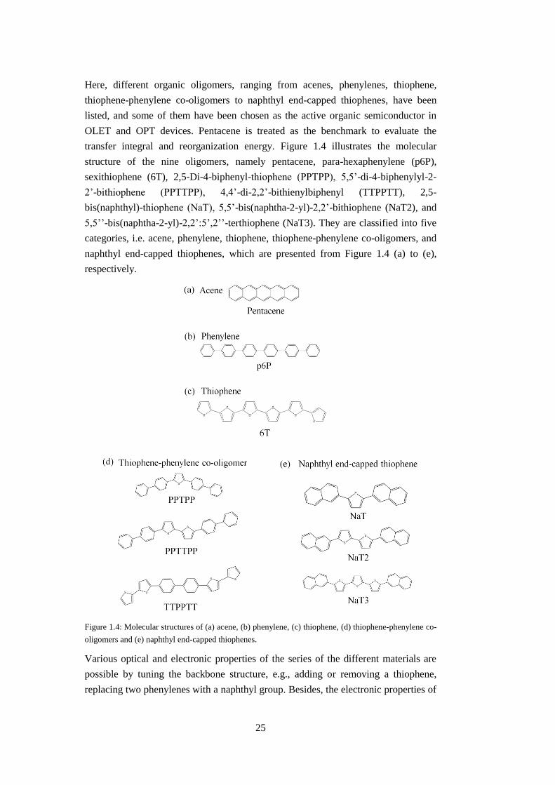
Here, different organic oligomers, ranging from acenes, phenylenes, thiophene,
thiophene-phenylene co-oligomers to naphthyl end-capped thiophenes, have been
listed, and some of them have been chosen as the active organic semiconductor in
OLET and OPT devices. Pentacene is treated as the benchmark to evaluate the
transfer integral and reorganization energy. Figure 1.4 illustrates the molecular
structure of the nine oligomers, namely pentacene, para-hexaphenylene (p6P),
sexithiophene (6T), 2,5-Di-4-biphenyl-thiophene (PPTPP), 5,5’-di-4-biphenylyl-2-
2’-bithiophene (PPTTPP), 4,4’-di-2,2’-bithienylbiphenyl (TTPPTT), 2,5-
bis(naphthyl)-thiophene (NaT), 5,5’-bis(naphtha-2-yl)-2,2’-bithiophene (NaT2), and
5,5’’-bis(naphtha-2-yl)-2,2’:5’,2’’-terthiophene (NaT3). They are classified into five
categories, i.e. acene, phenylene, thiophene, thiophene-phenylene co-oligomers, and
naphthyl end-capped thiophenes, which are presented from Figure 1.4 (a) to (e),
respectively.
Figure 1.4: Molecular structures of (a) acene, (b) phenylene, (c) thiophene, (d) thiophene-phenylene co-
oligomers and (e) naphthyl end-capped thiophenes.
Various optical and electronic properties of the series of the different materials are
possible by tuning the backbone structure, e.g., adding or removing a thiophene,
replacing two phenylenes with a naphthyl group. Besides, the electronic properties of
26
the organic crystals are also determined by the intermolecular interactions of
oligomers coupled by the van der Waals force. The parameters governing the
electronic transport characteristics will be discussed in Section 2.1.4.
1.2.2 Morphology: thin films and nanofibers
The morphology of organic semiconductors is usually the thin film. Organic thin
films are normally prepared by thermal vacuum evaporation [27], spin-coating [26]
or inkjet printing [28], which can lead to amorphous or semi-crystalline micro
structure. It is widely known that the performance of these thin film-based
optoelectronic devices can be affected by the presence of grain boundaries, charge
carrier traps and defects.
Under certain conditions, the organic materials can exhibit well ordered crystalline
structure, such as nanofibers. In contrast to the organic thin films, one-dimensional
organic nanofibers possess superior defect-free and highly ordered crystalline micro
structure, which are more suitable to be integrated into high-performance micro- or
nano-scale optoelectronic devices [29-31]. They can be grown by thermal
evaporation of organic small molecules under high vacuum conditions onto specific
surfaces, e.g. muscovite mica [29,86] and potassium chloride (KCl) [87]. For
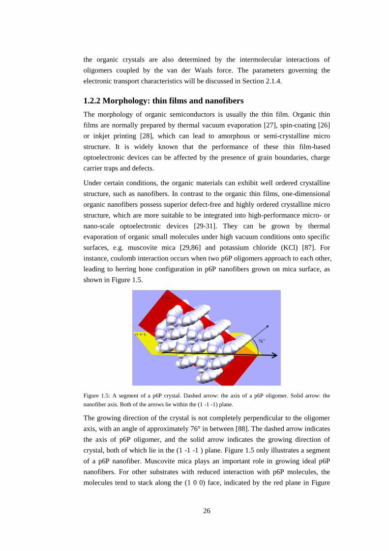
instance, coulomb interaction occurs when two p6P oligomers approach to each other,
leading to herring bone configuration in p6P nanofibers grown on mica surface, as
shown in Figure 1.5.
Figure 1.5: A segment of a p6P crystal. Dashed arrow: the axis of a p6P oligomer. Solid arrow: the
nanofiber axis. Both of the arrows lie within the (1 -1 -1) plane.
The growing direction of the crystal is not completely perpendicular to the oligomer
axis, with an angle of approximately 76° in between [88]. The dashed arrow indicates
the axis of p6P oligomer, and the solid arrow indicates the growing direction of
crystal, both of which lie in the (1 -1 -1 ) plane. Figure 1.5 only illustrates a segment
of a p6P nanofiber. Muscovite mica plays an important role in growing ideal p6P
nanofibers. For other substrates with reduced interaction with p6P molecules, the
molecules tend to stack along the (1 0 0) face, indicated by the red plane in Figure
27
1.5, resulting in layers of upright molecules [88]. In contrast to such substrates, the
surface of muscovite mica has relatively high interaction with p6P molecules due to
being positively charged and polar after cleavage. The p6P nanofiber dimension is
normally several ten nanometers in height, several hundred nanometers in width and
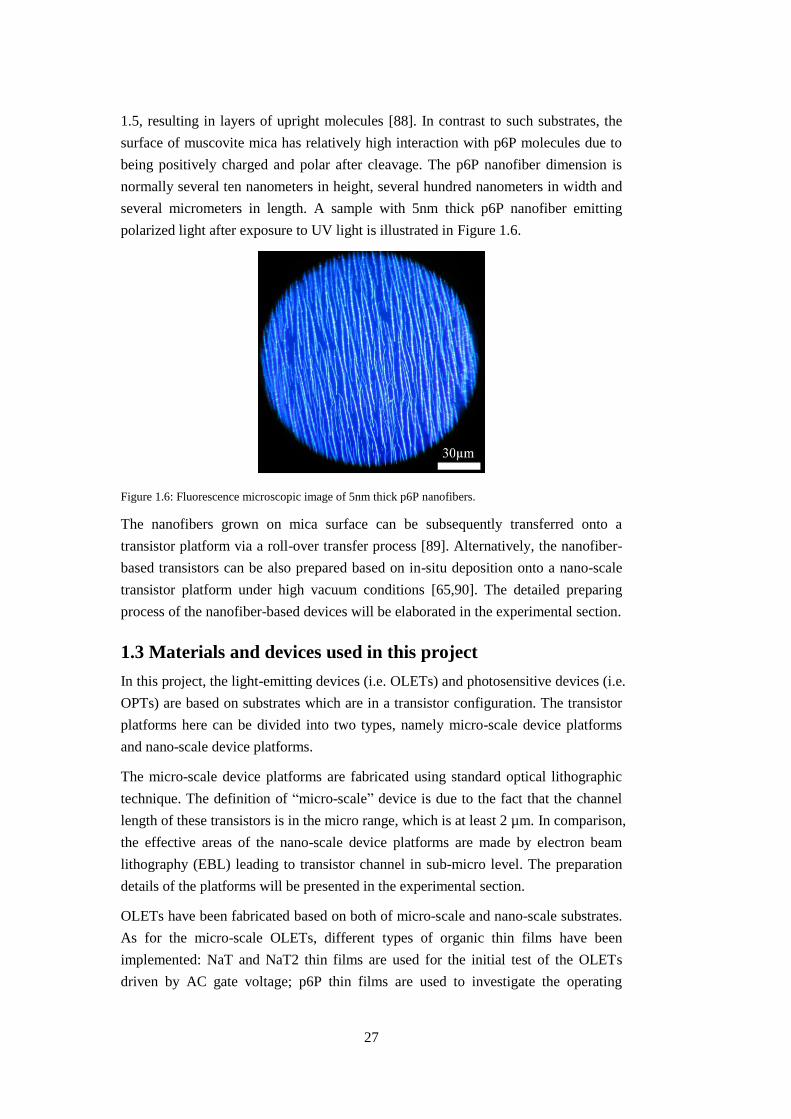
several micrometers in length. A sample with 5nm thick p6P nanofiber emitting
polarized light after exposure to UV light is illustrated in Figure 1.6.
Figure 1.6: Fluorescence microscopic image of 5nm thick p6P nanofibers.
The nanofibers grown on mica surface can be subsequently transferred onto a
transistor platform via a roll-over transfer process [89]. Alternatively, the nanofiber-
based transistors can be also prepared based on in-situ deposition onto a nano-scale
transistor platform under high vacuum conditions [65,90]. The detailed preparing
process of the nanofiber-based devices will be elaborated in the experimental section.
1.3 Materials and devices used in this project
In this project, the light-emitting devices (i.e. OLETs) and photosensitive devices (i.e.
OPTs) are based on substrates which are in a transistor configuration. The transistor
platforms here can be divided into two types, namely micro-scale device platforms
and nano-scale device platforms.
The micro-scale device platforms are fabricated using standard optical lithographic
technique. The definition of “micro-scale” device is due to the fact that the channel
length of these transistors is in the micro range, which is at least 2 µm. In comparison,
the effective areas of the nano-scale device platforms are made by electron beam
lithography (EBL) leading to transistor channel in sub-micro level. The preparation
details of the platforms will be presented in the experimental section.
OLETs have been fabricated based on both of micro-scale and nano-scale substrates.
As for the micro-scale OLETs, different types of organic thin films have been
implemented: NaT and NaT2 thin films are used for the initial test of the OLETs
driven by AC gate voltage; p6P thin films are used to investigate the operating
28
mechanism of AC biased OLET. Transferred p6P nanofibers have also been applied
in the micro-scale OLETs for the initial test. Regarding the nano-scale devices, in-
situ grown p6P and 6T nanofibers can bridge across the transistor channel directly
due to the narrow sub-micro channel between the EBL fabricated electrodes.
OPTs have been fabricated only on micro-scale substrates, using both of NaT2 thin
films and transferred NaT2 nanofibers. NaT2 thin film transistors are treated as the
reference to compare with the crystalline nanofiber-based OPT devices.
For clarity, the organic semiconductors in different morphologies implemented in
OLETs and OPTs are listed in Table 1.1.
Table 1.1: Organic semiconductors in different morphologies implemented in OLETs and OPTs.
micro-scale OLET nano-scale OLET micro-scale OPT
thin films NaT, NaT2, p6P,PPTPP (none) NaT2
transferred nanofibers p6P (none) NaT2
in-situ grown nanofibers (none) p6P, 6T (none)
1.4 Structure of the thesis
The thesis consists of six chapters, and brief descriptions of each chapter are as
follows:
Chapter 1: This chapter has presented an overview of applications of organic
optoelectronics, and in particular, OLEDs and OLETs as light sources, as well as
OPTs as light detectors are introduced in more details. Afterwards, organic materials
based on small molecules, which can form thin films with inferior molecular
ordering and crystalline nanofibers as the building blocks of the optoelectronic
devices, are described.
Chapter 2: This chapter presents a theoretical description of the charge carrier
injection from metal electrodes to organic semiconductors, e.g., space-charge field
assisted tunneling. It also provides a computational chemistry view of the molecular
orbitals, energy levels and intrinsic charge transport in organic crystals.
Chapter 3: This chapter provides the detailed experimental work of micro-scale
OLETs based on organic thin films and transferred nanofibers. It includes optical
measurements of OLETs and related electrical measurements of OFETs. An
operating mechanism of the AC biased OLETs, which involves space-charge field
assisted charge carrier injection is proposed.
29
Chapter 4: The nano-scale OLETs based on in-situ grown nanofibers have been
investigated. The proposed operating mechanism involving space-charge field
assisted charge carrier injection can also be applied to nano-scale devices.
Chapter 5: This chapter provides the experimental work of the OPTs based on micro-
scale transistor platforms. Both of organic thin films and nanofibers have been
implemented as the active organic materials, and the device performance based on
the materials with different morphologies has been compared.
Chapter 6: This chapter gives a summary of the theoretical and experimental work
presented in this thesis, and it envisions possible improvement and potential novel
applications of the organic optoelectronic devices.

30
31
Chapter 2: Charge injection and transport
The combination of metal electrodes and organic semiconductors is widely applied in
organic optoelectronic devices. The interfacial electronic structure between metal and
an organic material is therefore one critical factor to determine the device
performance. The alignment between the metal work function and the organic energy
level is essential in light-emitting mechanism.
The performance of optoelectronic devices depends on a large number of factors,
such as the intrinsic properties of active organic materials, the device configuration,
the characteristics of the semiconductor/insulator interface, etc. Among them, the
intrinsic property of the active organic material is the prerequisite factor to determine
the charge transport in the semiconductor device.
This chapter begins with a theoretical introduction of the charge injection and
transport, which involves energy levels, different theoretical models regarding charge
injection, calculation tools, and various intrinsic parameters (i.e., transfer integral,
reorganization energy, and charge carrier mobility) regarding the charge transport.
The corresponding calculations are subsequently provided.
2.1 Theory
2.1.1 Energy levels
In organic semiconductors, charge is localized on single molecules. The most
important molecular orbitals of these molecules are the highest occupied molecular
orbital (HOMO) and lowest unoccupied molecular orbital (LUMO), which can be
regarded as being equivalent to the valence bands and the conduction bands in
inorganic semiconductors, respectively [91]. The energy gap (Eg) of HOMO and
LUMO levels, together with vibronic energy levels of each electronic energy level,
determine the characteristics of the absorption and emission spectra of the organic
material [92-94].
When the organic semiconductor of an organic transistor has intimate contact with
metal electrodes, the band structure for the organic material and two metal electrodes
can be simplified as Figure 2.1. The vacuum level is defined as the level from which
electrons can escape from the atoms. The energy separation from HOMO level or
LUMO level to the vacuum level is defined as the ionization energy and the electron
affinity of the organic semiconductor, respectively. Under voltage bias, the holes or
32
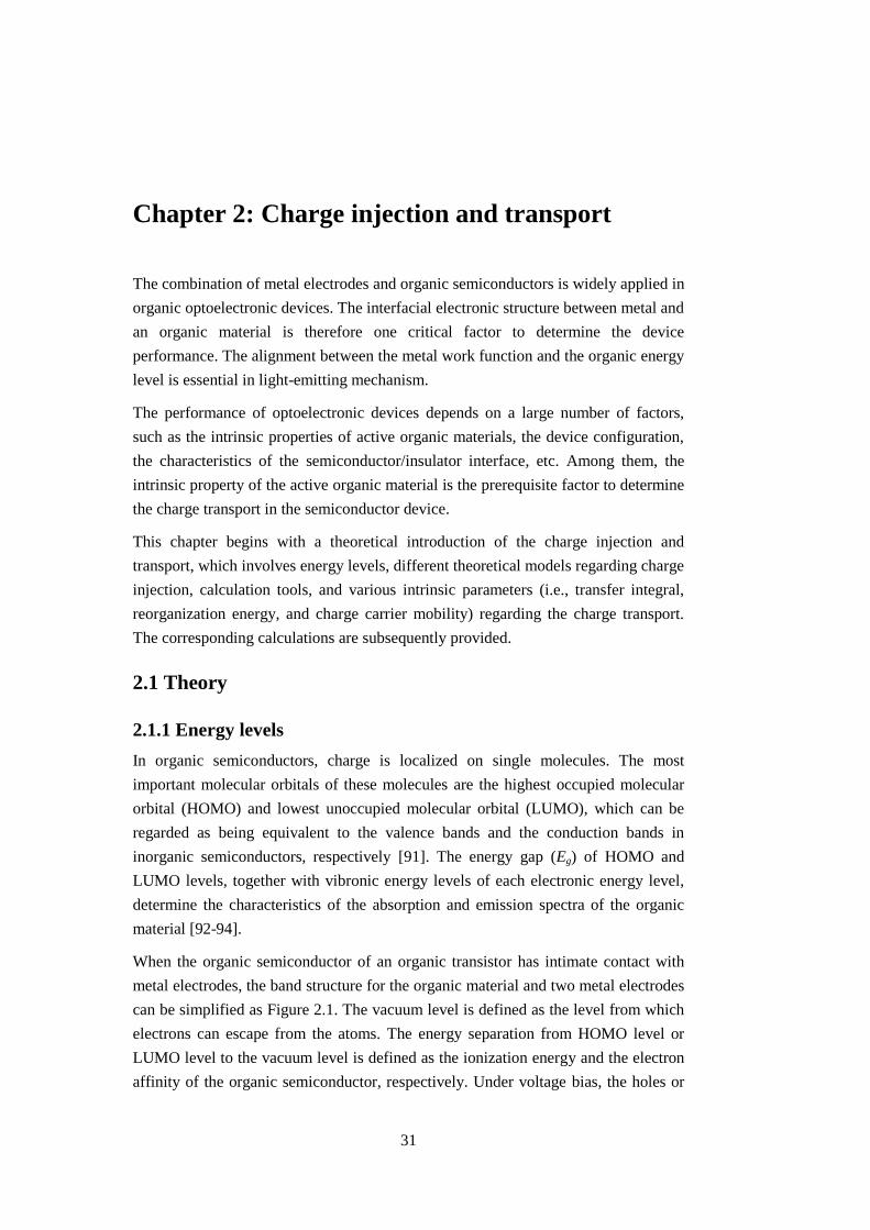
electrons can be injected from the metal electrode to the organic semiconductor. If
the HOMO level is shallower than the metal work function, the energy separation
from the gold work function to the HOMO level of organic semiconductor is the hole
injection barrier Φh. Likewise, if the LUMO level is higher than the metal work
function, the energy separation from the metal work function to the LUMO level of
organic semiconductor is the electron injection barrier Φe.
Figure 2.1: Schematic illustration of energy levels when the organic semiconductor and metal electrodes
have contact. Φh and Φe are the energy barriers for hole and electron injection, respectively.
Based on the dominant charge carriers injected and transported in the transistor
channel, the organic transistors can be classified as p-type (holes as main charge
carriers) and n-type (electrons as main charge carriers). When the holes and electrons
are nearly symmetrically injected from metal electrodes on both sides into organic
semiconductor, it is denoted as the ambipolar transport [53]. If the work function of
metal electrode is aligned with the LUMO or HOMO level of organic layer well, an
ohmic contact is formed at the interface, which can facilitate efficient charge
injection. However in practice, the work function of the metal electrode is usually
misaligned with the energy levels of the organic semiconductor, a Schottky barrier is
formed and the holes or electrons from metal electrodes should surmount the above-
mentioned injection barrier so as to inject into the organic semiconductor [95-96].
Self-assembled monolayer (SAM) can be used to modify the metal electrodes in
order to facilitate the charge carrier injection, and SAM deposition is especially
suitable for transistors with BC/BG configuration due to the fact that the SAM can be
prepared directly on the electrodes before deposition of the organic semiconductors
[97-100]. For the surface of gold (Au) electrodes, alkanethiols are often used to
modify the work function and affect the interface dipole because of the tight bond
between thiol and Au [101-102]. In this work, two types of SAMs, i.e.,
octadecanethiol (ODT, linear formula: CF3(CH2)17SH) and 1H,1H,2H,2H-
Perfluorodecanethiol (PFDT, linear formula: CF3(CF2)7(CH2)2SH) were utilized to
modify the Au surface before depositing PPTPP organic thin films to investigate the
change in charge injection in a transistor platform. Also, the SAM ODT and PFDT
were applied to modify the Au/p6P thin film interface in OLETs. Due to opposite
dipoles of the two monolayers, ODT is expected to lower the electrode work function,
33
while PFDT is expected to increase the electrode work function [103-105]. Therefore,
in a view of charge injection from the Au electrode to organic semiconductor, the
monolayer ODT will increase the hole injection barrier, while PFDT will decrease
the injection barrier.
2.1.2 Theoretical approaches to charge injection
There have been a great number of investigations on the charge injection from metal
electrodes to organic semiconductors [106-110]. The early theoretical investigations
generally neglected the localized polarons formed by charge carriers in organic
semiconductors. The theory developed by Richardson et al. considered the
thermionic emission of electrons from a metal surface and the electrons are
considered to be wave-like [111], which can only be generalized to the injection from
a metal into a theoretically perfect crystalline semiconductor [5]. Bethe et al.
investigated the case that charge carriers leave a crystalline semiconductor and enter
a metal ballistically, and a counter flowing electron current was considered [109].
Schottky and Crowell considered the effect of scattering and diffusion, and a
preexponential factor containing the charge density of states was utilized in their
drift-diffusion equation [112-113].
Various models considering the energetic disorder of organic semiconductors have
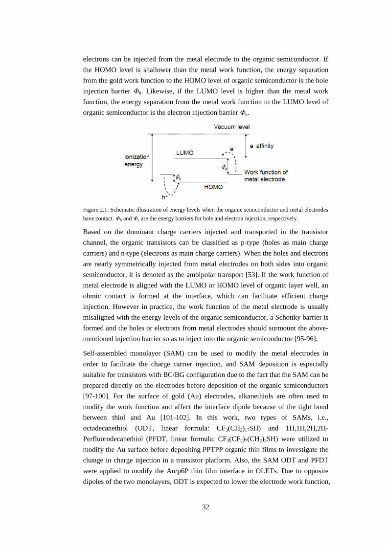
been developed [108,114-115], and the energy distributions follow a Gaussian
density of states, as illustrated in Figure 2.2. Here, p6P and Au are treated as the
organic semiconductor and metal electrode, respectively. The practical work function
of the Au electrode is typically 5.1 eV [116], and the HOMO level of p6P is 6.0 eV
[63]. Therefore a hole injection barrier of 0.9 eV can be expected. The charge
injection in these models considering energetic disorders normally has two steps. The
first step is that the charge carriers inject from the metal into the localized states of
the organic semiconductor as shown in Figure 2.2; the second step is that the carriers
either return to the metal or escape diffusively into the organic material.
Figure 2.2: Schematic illustration of the hole injection from metal to a localized state into p6P.
Reproduced from [30].
34
In this work, the model based on thermally assisted tunneling developed by Arkhipov
et al. has been applied to study hole injection into the hopping state distribution of
the organic semiconductor (p6P here) [108]. In this model, the hole injection occurs
over/through a potential barrier U(x) given by
2
0
( )16 r
qU x qFx
x
Eq. (2.1)
where x is distance from the metal electrode, φ is the energy difference between the
work function of Au and the HOMO level of p6P, ε0εr is the dielectric constant, q is
the elementary charge, and F is the external field strength. The hole injection is
considered including either the return of the charge-carrier to the metal electrode or
the diffusive escape from the image potential to the semiconductor bulk. Therefore,
the injected current Iinj can be described in terms of the tunneling probability
0exp( 2 )x (x0 is the distance from the contact the charge-carrier made the first
jump) and the escape probability wexc (x0)
0 0 0 0exp( 2 ) ( ) ( ) [ ( ) ]inj esca
I dx x w x dEBol E g U x E
Eq. (2.2)
where is the inverse localization radius and a is the nearest neighbor distance. The
escape probability wexc (x0) is the probability that a jumped carrier will avoid surface
recombination, which is determined by
0
00
0
exp[ ( )]16
( )
exp[ ( )]16
x
aB r
exc
aB r
e edx F x
k T xw x
e edx F x
k T x
. Eq. (2.3)
Bol(E) is a Boltzmann factor defined as
exp( ) 0;( )
1 0.
B
EE
k TBol E
E
Eq. (2.4)
The Gaussian energy distribution with an energy width σ is given by
2
0
2( ) exp( )
22
N Eg E
Eq. (2.5)
where N0 is the density of p6P molecules.
It should be noted that a model based on Fowler-Nordheim (F-N) tunneling is usually
considered in terms of inorganic devices when extremely high electrical field is
involved [117]. Even though an F-N plot can also be used to describe the relation
between the current and stimulated electrical field in organic optoelectronic devices,
the F-N tunneling is not part of the underlying operating mechanism [63-64].
35
2.1.3 Introduction of density functional theory (DFT) and basis sets
Quantum chemical modeling is useful to predict the intrinsic properties of organic
semiconductors, so as to facilitate the synthesis and selection of novel organic
optoelectronic materials. The powerful theoretical tool DFT is usually involved
[93,118-122]. The basis of the quantum chemical calculations is the well-known
Schrödinger equation [123]. It describes the changes of the quantum state of a
physical system, with the general form
2 ( , ) ( , )
2
r tV r t i
m t
Eq. (2.6)
where 2 is the Laplace operator in three dimensions. The Schrödinger equation
describes a single particle with mass m moving through space and time under the
influence of an external field .V is the reduced Planck’s constant, is the wave
function representing the probability amplitude for the particle to be found at position
r and at time t. The Schrödinger equation can only be exactly solved for atoms with
only one electron. Regarding a multi-electron system, no exact solutions can be
found. In this case, the Hartree-Fock method can be used to solve the Schrödinger
equation approximately. The Hartree-Fock method is based on the variation theorem,
which states that any approximation will have an expectation energy value being
greater than or equal to the true energy. Consequently, the better approximated wave
function is obtained with the first derivative of the energy approaching to zero. More
detailed can be found in Ref. [123].
The Hartree-Fock method provides the basis for the ab initio molecular orbital
calculation, which refers to a quantum mechanical method in which only physical
constants are provided as the calculation input. The most basic ab initio method
assumes that the electrons move in an averaged potential of the other electrons
without considering the instantaneous Coulombic repulsion among adjacent electrons.
Unlike the Hartree-Fock method, in DFT calculations, the properties of a multi-
electron system can be expressed as functional, which is a function of another
function, i.e. electron density. By doing so, the total electronic energy of a system
and its overall electronic density are correlated, which transfers the study object from
the wavefunctions of a N electron system with 3N spatial coordinates in Hartree-Fock
method to the same N electron system with only 3 spatial coordinates for its electron
density.
The basis sets used in the quantum chemical modeling are a set of trial orbitals,
which can give another set of solutions after iteration during calculations, and then
this set of solutions is used for the next iteration, likewise, until the convergence is
achieved. The basis sets are typically a combination of Gaussian orbitals, which have
the form of xay
bz
cexp(-α∙r
2) in Cartesian coordinates, where α determines the degree
36
of spreading of the Gaussian function, e.g. a function with a small value of α spreads
relatively far. The sum of a, b and c determines the type of orbital. For instance,
a+b+c=1 indicates a p-orbital.
Since generally only the valence electrons take part in most of the molecular bonding,
it is common to double the functions used to describe the valence orbitals, whereas
the inner shells are represented by single functions. This is called split valence
double zeta basis sets, with a typical notation of X-YZg, where X represents the
number of Gaussian functions describing the core orbitals, Y and Z indicate that the
valence orbitals are consisted of two basis functions, Y for contracted part and Z for
diffuse part. For instance, 6-31g indicates that six Gaussian functions are used to
describe the inner orbitals, while the valence orbitals are represented by three
Gaussian functions for the contracted part and one Gaussian function for the diffuse
part. Usually, polarization functions need to be added into the basis sets, which is
indicated by one asterisk (*) for adding polarization only for heavy atoms, or two
asterisks (**) for adding polarization both for heavy atoms and hydrogen atoms.
When it comes to anions and other molecules with a significant amount of electron
density away from the nuclear centers, highly diffuse functions are important to be
introduced, which are denoted by one plus sign (+) for heavy atoms, or two plus
signs (++) both for heavy atoms and hydrogen atoms.
The abovementioned basis sets are examples used in the computational chemistry
software Gaussian 09 [124], while some similar basis sets can only be used in
another computational type of software. For instance, Double Zeta Polarization (DZP)
is implemented in Amsterdam Density Functional (ADF).
2.1.4 Intrinsic charge transport
In organic semiconductors, charges are localized on single molecule, and the charge
transport in this localized system is mainly a hopping process from one molecule to a
neighboring molecule. This hopping regime of charge transport in organic materials
is important in determining the performance of optoelectronic devices. The intersite
charge transfer rate kij in this hopping regime is given in the semi-classical
approximation by the Marcus equation [125],
2
2
2
( )exp( )
4
ij ij
ij ij
B ij ij B
Ek t
k T k T
Eq. (2.7)
where is the reduced Planck’s constant, ΔEij is the energy difference between the
initial and final site energy, kB and T are the Boltzmann constant and the temperature,
respectively. The transfer integral tij and the reorganization energy λij are the
predominant factors to determine the charge transfer rate, whereas ΔEij is often
insignificant [126].
37
The transfer integral describes the energy gained by electron delocalization among
neighboring molecules, and it depends largely on orbital overlap [127]. The
calculation of the transfer integral, considering the polarization effects between
asymmetry molecules, is usually based on the Kohn-Sham equation [123]. The
Kohn-Sham equation can be described in a matrix form when only a dimer is
considered
HC SCE Eq. (2.8)
where S is the overlap matrix and the Kohn-Sham matrix H is given by
1 12
12 2
e tH
t e
. Eq. (2.9)
The elements of the Kohn-Sham matrix can be expressed as
ij i jH Eq. (2.10)
where H is the Hamiltonian operator of the Kohn-Sham equation. In Eq. (2.10), Hij
stands for the site energy e when i = j; while Hij is the transfer integral t when i ≠ j.
The orbitals i used in Eq. (2.10) are nonorthogonal. An orthogonal basis set is
required and the effective transfer integral can be obtained using Löwdin’s
symmetric transformation [128] as
12 1 2 12
12 2
12
1( )
2
1
eff
t e e S
tS
. Eq. (2.11)
Next, the matrix S is set to identity matrix, and Eq. (2.8) can be expressed in the
orthonormal basis as a standard eigenvalue equation
effH C CE . Eq. (2.12)
The reorganization energy is the energy cost accompanying the geometric relaxation
of an oligomer associated with the charge transfer [127]. Assuming the transfer
integral is constant, the charge transfer rate increases with decreasing reorganization
energy. The reorganization energy consists of inter- and intra-molecule contributions.
The inter-molecule reorganization energy is attributed to the electronic and nuclear
polarization/relaxation of the surrounding environment, which means that the
adjacent molecules with respect to the target molecule should also be considered
during calculation. The intra-molecule reorganization energy results from the
changes in equilibrium geometries of the donor and acceptor molecules during the
charge transfer process. It can be determined by summing up two relaxation energies:
the relaxation of the donor molecule upon going from the charged-state geometry to
the neutral-state geometry, i.e., λ0 = E01-E00; and the relaxation of the acceptor
38
molecule upon going from the neutral-state geometry to the charged-state geometry,
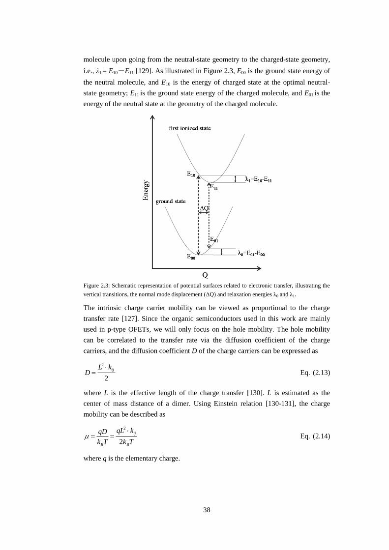
i.e., λ1 = E10-E11 [129]. As illustrated in Figure 2.3, E00 is the ground state energy of
the neutral molecule, and E10 is the energy of charged state at the optimal neutral-
state geometry; E11 is the ground state energy of the charged molecule, and E01 is the
energy of the neutral state at the geometry of the charged molecule.
Figure 2.3: Schematic representation of potential surfaces related to electronic transfer, illustrating the
vertical transitions, the normal mode displacement (ΔQ) and relaxation energies λ0 and λ1.
The intrinsic charge carrier mobility can be viewed as proportional to the charge
transfer rate [127]. Since the organic semiconductors used in this work are mainly
used in p-type OFETs, we will only focus on the hole mobility. The hole mobility
can be correlated to the transfer rate via the diffusion coefficient of the charge
carriers, and the diffusion coefficient D of the charge carriers can be expressed as
2
2
ijL kD
Eq. (2.13)
where L is the effective length of the charge transfer [130]. L is estimated as the
center of mass distance of a dimer. Using Einstein relation [130-131], the charge
mobility can be described as
2
2
ij
B B
qL kqD
k T k T
Eq. (2.14)
where q is the elementary charge.
39
2.2 Calculations
2.2.1 Energy levels
An appropriate organic semiconductor with suitable HOMO/LUMO level is very
important for photosensitive devices, such as phototransistors. The energy gap Eg
between HOMO and LUMO levels determines the range of incident light which can
be absorbed or detected by the phototransistor, because only incident photons with
higher energy than Eg can excite the electrons from the HOMO to the LUMO level
[93,132-133]. The better alignment of HOMO/LUMO levels with metal work
function is also important to the subsequent charge carrier collection through the
metal electrodes.
Figure 2.4: HOMO/LUMO of various materials calculated by PW91 using Gaussian 09. The values
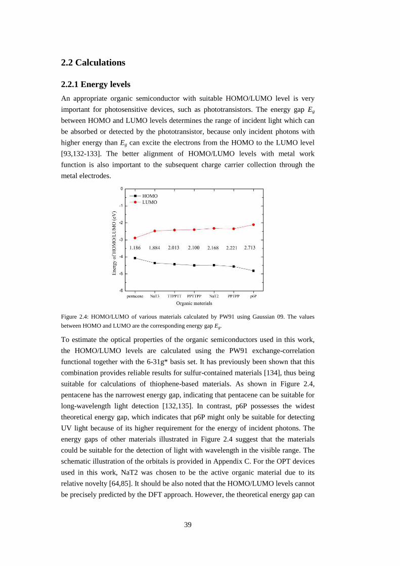
between HOMO and LUMO are the corresponding energy gap Eg.
To estimate the optical properties of the organic semiconductors used in this work,
the HOMO/LUMO levels are calculated using the PW91 exchange-correlation
functional together with the 6-31g* basis set. It has previously been shown that this
combination provides reliable results for sulfur-contained materials [134], thus being
suitable for calculations of thiophene-based materials. As shown in Figure 2.4,
pentacene has the narrowest energy gap, indicating that pentacene can be suitable for
long-wavelength light detection [132,135]. In contrast, p6P possesses the widest
theoretical energy gap, which indicates that p6P might only be suitable for detecting
UV light because of its higher requirement for the energy of incident photons. The
energy gaps of other materials illustrated in Figure 2.4 suggest that the materials
could be suitable for the detection of light with wavelength in the visible range. The
schematic illustration of the orbitals is provided in Appendix C. For the OPT devices
used in this work, NaT2 was chosen to be the active organic material due to its
relative novelty [64,85]. It should be also noted that the HOMO/LUMO levels cannot
be precisely predicted by the DFT approach. However, the theoretical energy gap can
40
be reliable. For instance, the theoretical energy gap of p6P is about 10%
underestimated by the DFT calculations, in comparison with the experimental value
(3.0 eV) [63].
2.2.2 Transfer integral
The transfer integral calculations were carried out using a combination of PW91/6-
31g* level of theory. Since the transfer integral is assimilated to the electronic
coupling among neighboring molecules during the hopping regime of the charge
transfer process [127], it is largely dictated by the orbital overlap, which describes
the overlap of particular obitals determined by the mutual separation and orientations
of the neighboring molecules [136]. Therefore, larger values of transfer integral are
usually expected along the direction in which the distance between the two
neighboring molecules is nearer. In practice, this distance along the transverse
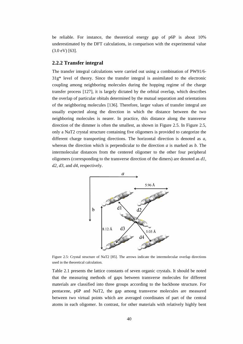
direction of the dimmer is often the smallest, as shown in Figure 2.5. In Figure 2.5,
only a NaT2 crystal structure containing five oligomers is provided to categorize the
different charge transporting directions. The horizontal direction is denoted as a,
whereas the direction which is perpendicular to the direction a is marked as b. The
intermolecular distances from the centered oligomer to the other four peripheral
oligomers (corresponding to the transverse direction of the dimers) are denoted as d1,
d2, d3, and d4, respectively.
Figure 2.5: Crystal structure of NaT2 [85]. The arrows indicate the intermolecular overlap directions
used in the theoretical calculation.
Table 2.1 presents the lattice constants of seven organic crystals. It should be noted
that the measuring methods of gaps between transverse molecules for different
materials are classified into three groups according to the backbone structure. For
pentacene, p6P and NaT2, the gap among transverse molecules are measured
between two virtual points which are averaged coordinates of part of the central
atoms in each oligomer. In contrast, for other materials with relatively highly bent
41
backbone structure, the virtual points are averaged coordinates of all the atoms in
each oligomer.
Table 2.1 Lattice constants in direction a and b, and distances between transverse molecules in various
organic materials.
materials lattice constant in
direction a [Å]
lattice constant in
direction b [Å]
gaps between transverse
oligomers [Å]
pentacene 6.266 7.775 d1=d4=4.76; d2=d3=5.21#
p6P 5.568 8.091 d1=d2=d3=d4=4.911*
PPTPP 5.793 7.497 d1=d2=4.64; d3=d4=4.77§
PPTTPP 5.708 7.604 d1=d3=5.0; d2=d4=5.0§
TTPPTT 5.824 7.294 d1=d3=5.0; d2=d4=5.0§
NaT2 5.964 8.120 d1=d2=d3=d4=5.05*
NaT3 5.917 7.866 d1=d3=4.74; d2=d4=5.10§
#: The gap is measured as the distance between two virtual points of corresponding oligomers, and each
virtual point is the averaged coordinate of the six carbon atoms in the center of each oligomer.
*: The gap is measured as the distance between two virtual points of corresponding oligomers, and each
virtual point is the averaged coordinate of the two carbon atoms in the center of each oligomer.
§: The gap is measured as the distance between two virtual points of corresponding oligomers, and each
virtual point is the averaged coordinate of all the atoms of each oligomer.
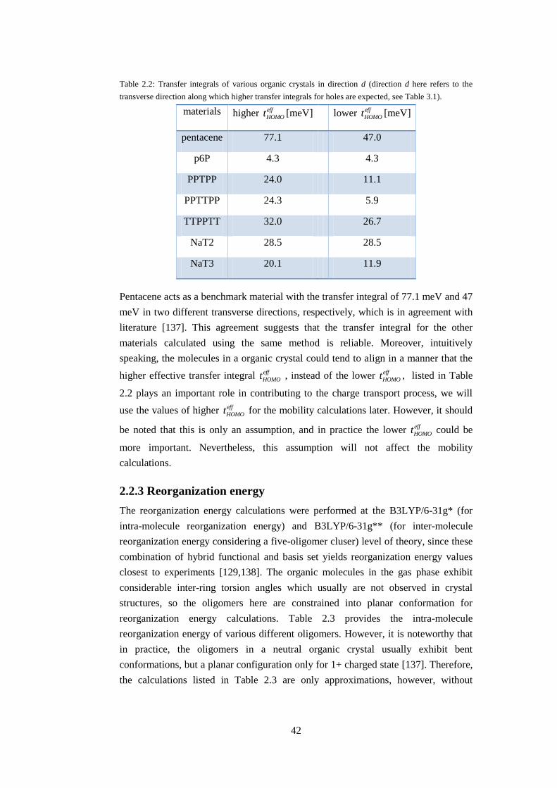
Since the transfer integral along the transverse direction is of great importance in
determining charge transport properties of organic crystals, the transfer integrals for
HOMO in direction d are listed in Table 2.2. It is necessary to be careful when
dealing with different transverse direction in organic crystals, since the symmetry is
not the same for different materials, as shown in Table 2.1. The symmetry
determination for different materials listed in Table 2.1 is further verified by direct
calculation of corresponding transfer integrals. For instance, the d directions of p6P
are all identical due to the same distance of mass center between the central oligomer
and the four peripheral oligomers, and this is confirmed by the fact that the transfer
integrals in the four directions are exactly the same. In contrast, according to the
distance measurement, the d1, d4 directions and the d2, d3 directions of the
pentacene crystal are identical, respectively. This is also confirmed by the
calculations that the transfer integrals of d1 and d4 direction of pentacene are the
same, and the transfer integrals of d2 and d3 direction are the same. It is noteworthy
that the effective transfer integral along d1 and d4 direction of pentacene is higher
than that along d2 and d3 direction, hence the denotation of higher eff
HOMOt and lower
eff
HOMOt , respectively, as shown in Table 2.2.
42
Table 2.2: Transfer integrals of various organic crystals in direction d (direction d here refers to the
transverse direction along which higher transfer integrals for holes are expected, see Table 3.1).
materials higher eff
HOMOt [meV] lower eff
HOMOt [meV]
pentacene 77.1 47.0
p6P 4.3 4.3
PPTPP 24.0 11.1
PPTTPP 24.3 5.9
TTPPTT 32.0 26.7
NaT2 28.5 28.5
NaT3 20.1 11.9
Pentacene acts as a benchmark material with the transfer integral of 77.1 meV and 47
meV in two different transverse directions, respectively, which is in agreement with
literature [137]. This agreement suggests that the transfer integral for the other
materials calculated using the same method is reliable. Moreover, intuitively
speaking, the molecules in a organic crystal could tend to align in a manner that the
higher effective transfer integral eff
HOMOt , instead of the lower eff
HOMOt , listed in Table
2.2 plays an important role in contributing to the charge transport process, we will
use the values of higher eff
HOMOt for the mobility calculations later. However, it should
be noted that this is only an assumption, and in practice the lower eff
HOMOt could be
more important. Nevertheless, this assumption will not affect the mobility
calculations.
2.2.3 Reorganization energy
The reorganization energy calculations were performed at the B3LYP/6-31g* (for
intra-molecule reorganization energy) and B3LYP/6-31g** (for inter-molecule
reorganization energy considering a five-oligomer cluser) level of theory, since these
combination of hybrid functional and basis set yields reorganization energy values
closest to experiments [129,138]. The organic molecules in the gas phase exhibit
considerable inter-ring torsion angles which usually are not observed in crystal
structures, so the oligomers here are constrained into planar conformation for
reorganization energy calculations. Table 2.3 provides the intra-molecule
reorganization energy of various different oligomers. However, it is noteworthy that
in practice, the oligomers in a neutral organic crystal usually exhibit bent
conformations, but a planar configuration only for 1+ charged state [137]. Therefore,
the calculations listed in Table 2.3 are only approximations, however, without
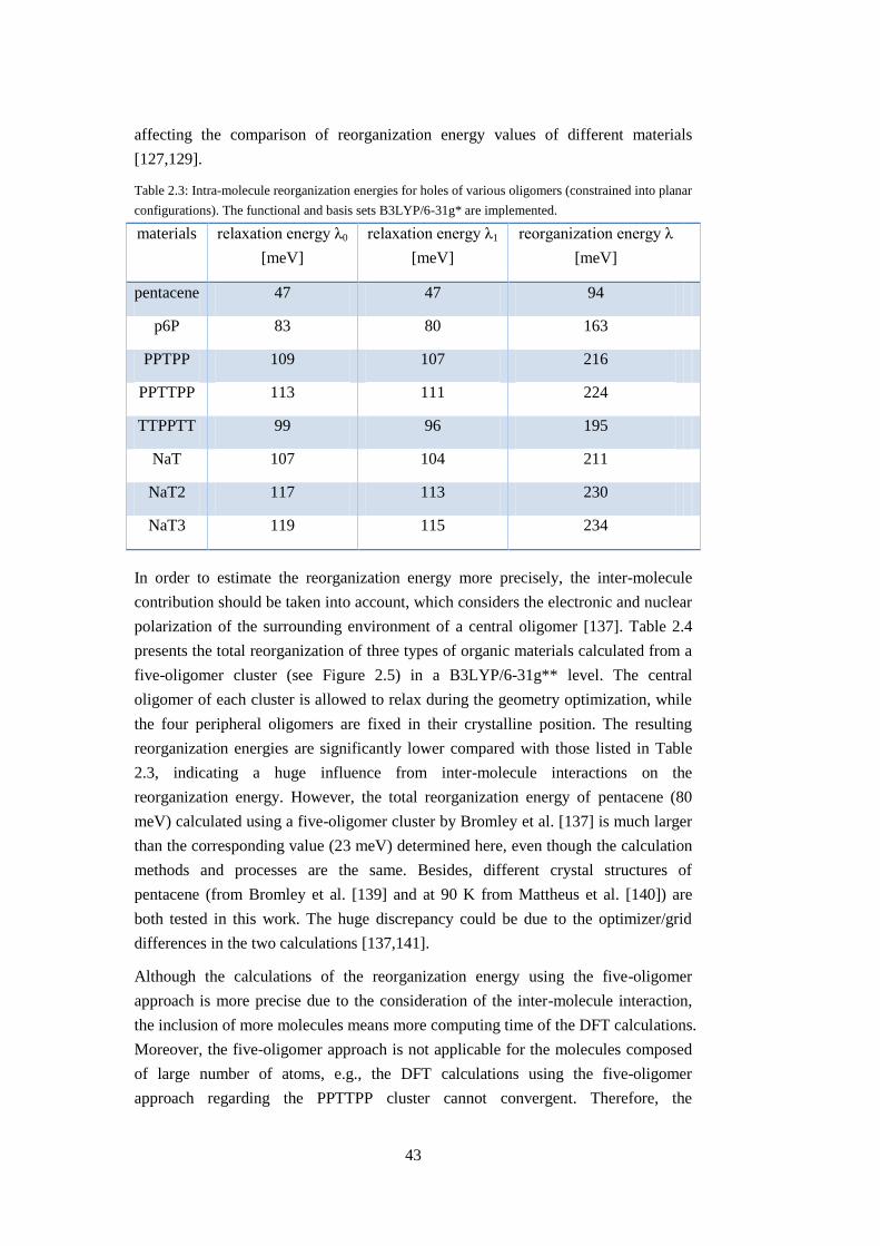
43
affecting the comparison of reorganization energy values of different materials
[127,129].
Table 2.3: Intra-molecule reorganization energies for holes of various oligomers (constrained into planar
configurations). The functional and basis sets B3LYP/6-31g* are implemented.
materials relaxation energy λ0
[meV]
relaxation energy λ1
[meV]
reorganization energy λ
[meV]
pentacene 47 47 94
p6P 83 80 163
PPTPP 109 107 216
PPTTPP 113 111 224
TTPPTT 99 96 195
NaT 107 104 211
NaT2 117 113 230
NaT3 119 115 234
In order to estimate the reorganization energy more precisely, the inter-molecule
contribution should be taken into account, which considers the electronic and nuclear
polarization of the surrounding environment of a central oligomer [137]. Table 2.4
presents the total reorganization of three types of organic materials calculated from a
five-oligomer cluster (see Figure 2.5) in a B3LYP/6-31g** level. The central
oligomer of each cluster is allowed to relax during the geometry optimization, while
the four peripheral oligomers are fixed in their crystalline position. The resulting
reorganization energies are significantly lower compared with those listed in Table
2.3, indicating a huge influence from inter-molecule interactions on the
reorganization energy. However, the total reorganization energy of pentacene (80
meV) calculated using a five-oligomer cluster by Bromley et al. [137] is much larger
than the corresponding value (23 meV) determined here, even though the calculation
methods and processes are the same. Besides, different crystal structures of
pentacene (from Bromley et al. [139] and at 90 K from Mattheus et al. [140]) are
both tested in this work. The huge discrepancy could be due to the optimizer/grid
differences in the two calculations [137,141].
Although the calculations of the reorganization energy using the five-oligomer
approach is more precise due to the consideration of the inter-molecule interaction,
the inclusion of more molecules means more computing time of the DFT calculations.
Moreover, the five-oligomer approach is not applicable for the molecules composed
of large number of atoms, e.g., the DFT calculations using the five-oligomer
approach regarding the PPTTPP cluster cannot convergent. Therefore, the
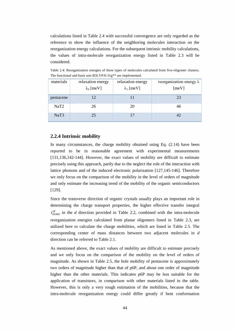
44
calculations listed in Table 2.4 with successful convergence are only regarded as the
reference to show the influence of the neighboring molecules interaction on the
reorganization energy calculations. For the subsequent intrinsic mobility calculations,
the values of intra-molecule reorganization energy listed in Table 2.3 will be
considered.
Table 2.4: Reorganization energies of three types of molecules calculated from five-oligomer clusters.
The functional and basis sets B3LYP/6-31g** are implemented.
materials relaxation energy
λ0 [meV]
relaxation energy
λ1 [meV]
reorganization energy λ
[meV]
pentacene 12 11 23
NaT2 26 20 46
NaT3 25 17 42
2.2.4 Intrinsic mobility
In many circumstances, the charge mobility obtained using Eq. (2.14) have been
reported to be in reasonable agreement with experimental measurements
[131,136,142-144]. However, the exact values of mobility are difficult to estimate
precisely using this approach, partly due to the neglect the role of the interaction with
lattice phonons and of the induced electronic polarization [127,145-146]. Therefore
we only focus on the comparison of the mobility in the level of orders of magnitude
and only estimate the increasing trend of the mobility of the organic semiconductors
[129].
Since the transverse direction of organic crystals usually plays an important role in
determining the charge transport properties, the higher effective transfer integral
eff
HOMOt in the d direction provided in Table 2.2, combined with the intra-molecule
reorganization energies calculated from planar oligomers listed in Table 2.3, are
utilized here to calculate the charge mobilities, which are listed in Table 2.5. The
corresponding center of mass distances between two adjacent molecules in d
direction can be referred to Table 2.1.
As mentioned above, the exact values of mobility are difficult to estimate precisely
and we only focus on the comparison of the mobility on the level of orders of
magnitude. As shown in Table 2.5, the hole mobility of pentacene is approximately
two orders of magnitude higher than that of p6P, and about one order of magnitude
higher than the other materials. This indicates p6P may be less suitable for the
application of transistors, in comparison with other materials listed in the table.
However, this is only a very rough estimation of the mobilities, because that the
intra-molecule reorganization energy could differ greatly if bent conformation
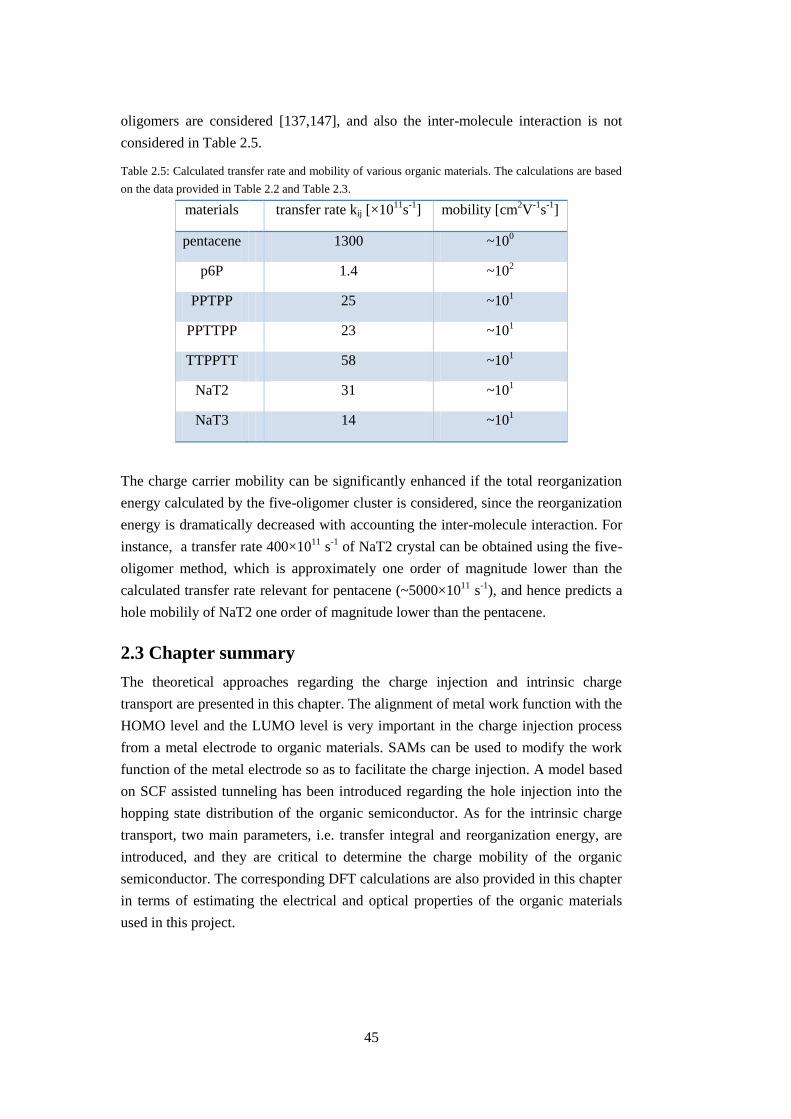
45
oligomers are considered [137,147], and also the inter-molecule interaction is not
considered in Table 2.5.
Table 2.5: Calculated transfer rate and mobility of various organic materials. The calculations are based
on the data provided in Table 2.2 and Table 2.3.
materials transfer rate kij [×1011
s-1
] mobility [cm2V
-1s
-1]
pentacene 1300 ~100
p6P 1.4 ~102
PPTPP 25 ~101
PPTTPP 23 ~101
TTPPTT 58 ~101
NaT2 31 ~101
NaT3 14 ~101
The charge carrier mobility can be significantly enhanced if the total reorganization
energy calculated by the five-oligomer cluster is considered, since the reorganization
energy is dramatically decreased with accounting the inter-molecule interaction. For
instance, a transfer rate 400×1011
s-1
of NaT2 crystal can be obtained using the five-
oligomer method, which is approximately one order of magnitude lower than the
calculated transfer rate relevant for pentacene (~5000×1011
s-1
), and hence predicts a
hole mobilily of NaT2 one order of magnitude lower than the pentacene.
2.3 Chapter summary
The theoretical approaches regarding the charge injection and intrinsic charge
transport are presented in this chapter. The alignment of metal work function with the
HOMO level and the LUMO level is very important in the charge injection process
from a metal electrode to organic materials. SAMs can be used to modify the work
function of the metal electrode so as to facilitate the charge injection. A model based
on SCF assisted tunneling has been introduced regarding the hole injection into the
hopping state distribution of the organic semiconductor. As for the intrinsic charge
transport, two main parameters, i.e. transfer integral and reorganization energy, are
introduced, and they are critical to determine the charge mobility of the organic
semiconductor. The corresponding DFT calculations are also provided in this chapter
in terms of estimating the electrical and optical properties of the organic materials
used in this project.

46
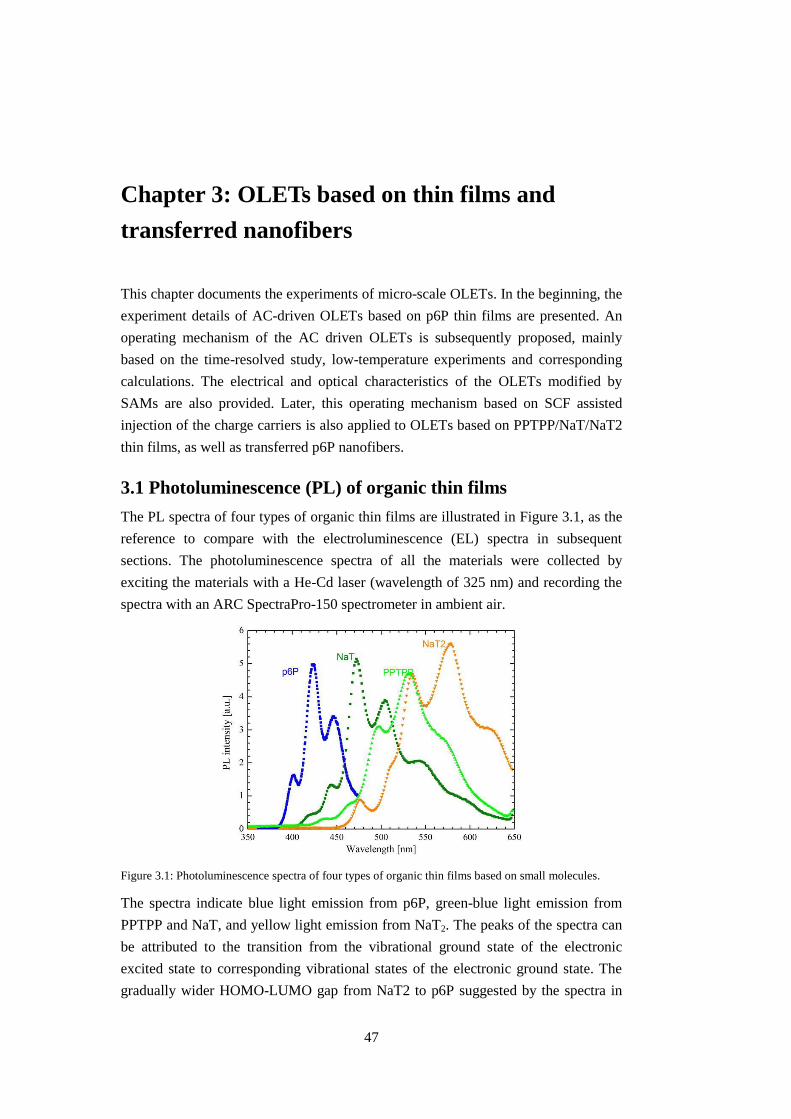
47
Chapter 3: OLETs based on thin films and
transferred nanofibers
This chapter documents the experiments of micro-scale OLETs. In the beginning, the
experiment details of AC-driven OLETs based on p6P thin films are presented. An
operating mechanism of the AC driven OLETs is subsequently proposed, mainly
based on the time-resolved study, low-temperature experiments and corresponding
calculations. The electrical and optical characteristics of the OLETs modified by
SAMs are also provided. Later, this operating mechanism based on SCF assisted
injection of the charge carriers is also applied to OLETs based on PPTPP/NaT/NaT2
thin films, as well as transferred p6P nanofibers.
3.1 Photoluminescence (PL) of organic thin films
The PL spectra of four types of organic thin films are illustrated in Figure 3.1, as the
reference to compare with the electroluminescence (EL) spectra in subsequent
sections. The photoluminescence spectra of all the materials were collected by
exciting the materials with a He-Cd laser (wavelength of 325 nm) and recording the
spectra with an ARC SpectraPro-150 spectrometer in ambient air.
Figure 3.1: Photoluminescence spectra of four types of organic thin films based on small molecules.
The spectra indicate blue light emission from p6P, green-blue light emission from
PPTPP and NaT, and yellow light emission from NaT2. The peaks of the spectra can
be attributed to the transition from the vibrational ground state of the electronic
excited state to corresponding vibrational states of the electronic ground state. The
gradually wider HOMO-LUMO gap from NaT2 to p6P suggested by the spectra in
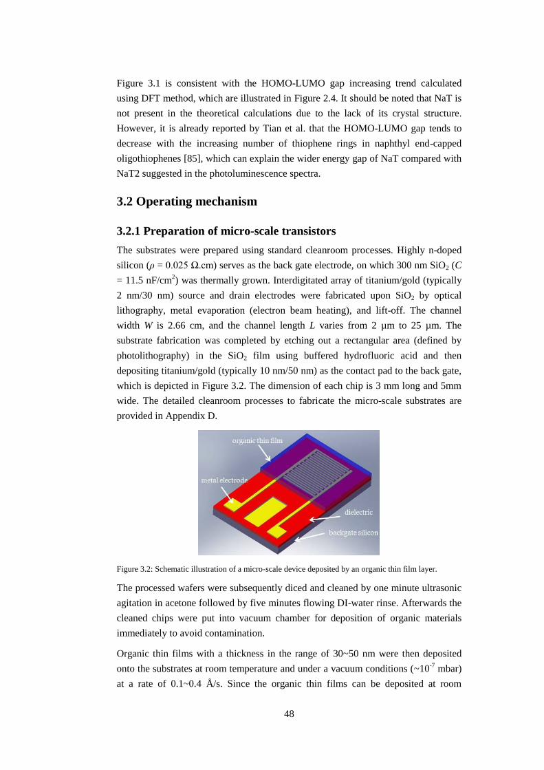
48
Figure 3.1 is consistent with the HOMO-LUMO gap increasing trend calculated
using DFT method, which are illustrated in Figure 2.4. It should be noted that NaT is
not present in the theoretical calculations due to the lack of its crystal structure.
However, it is already reported by Tian et al. that the HOMO-LUMO gap tends to
decrease with the increasing number of thiophene rings in naphthyl end-capped
oligothiophenes [85], which can explain the wider energy gap of NaT compared with
NaT2 suggested in the photoluminescence spectra.
3.2 Operating mechanism
3.2.1 Preparation of micro-scale transistors
The substrates were prepared using standard cleanroom processes. Highly n-doped
silicon (ρ = 0.025 Ω.cm) serves as the back gate electrode, on which 300 nm SiO2 (C
= 11.5 nF/cm2) was thermally grown. Interdigitated array of titanium/gold (typically
2 nm/30 nm) source and drain electrodes were fabricated upon SiO2 by optical
lithography, metal evaporation (electron beam heating), and lift-off. The channel
width W is 2.66 cm, and the channel length L varies from 2 µm to 25 µm. The
substrate fabrication was completed by etching out a rectangular area (defined by
photolithography) in the SiO2 film using buffered hydrofluoric acid and then
depositing titanium/gold (typically 10 nm/50 nm) as the contact pad to the back gate,
which is depicted in Figure 3.2. The dimension of each chip is 3 mm long and 5mm
wide. The detailed cleanroom processes to fabricate the micro-scale substrates are
provided in Appendix D.
Figure 3.2: Schematic illustration of a micro-scale device deposited by an organic thin film layer.
The processed wafers were subsequently diced and cleaned by one minute ultrasonic
agitation in acetone followed by five minutes flowing DI-water rinse. Afterwards the
cleaned chips were put into vacuum chamber for deposition of organic materials
immediately to avoid contamination.
Organic thin films with a thickness in the range of 30~50 nm were then deposited
onto the substrates at room temperature and under a vacuum conditions (~10-7
mbar)
at a rate of 0.1~0.4 Å/s. Since the organic thin films can be deposited at room
49
temperature, carbon taps which are vacuum compatible were directly put onto the
sample holder to carry the transistor substrates, as shown in Figure 3.3.
Figure 3.3: Schematic illustration of the micro-scale devices on the sample holder surface.
3.2.2 Electrical characteristics
In conventional DC-driven OLETs, electrons and holes are injected from opposite
metal electrodes and subsequently recombine in the transistor channel, leading to
light emission [53]. Sufficient injection and good transport of charge carriers are the
prerequisite factor to influence the optical property of the OLETs. For AC-driven
OLETs, electrons and holes can be injected from an individual metal electrode
during different operating regimes of the AC gate voltage, leading to EL in the
vicinity of one metal electrode [63-64,66]. The injection of electrons, for example,
can be affected by the space-charge field formed by previously injected holes, and
the injection of holes is the predominant factor to determine the AC-driven OLETs
[63]. Therefore, the electrical characterization of the corresponding OFETs is
necessary to evaluate the device performance of OLETs. In this project, The
electrical measurement was made using a home-made setup based on a Labview-
controlled data acquisition card in combination with a Stanford Research SR 570
current preamplifier and a Falco Systems WMA-280 voltage amplifier.
Figure 3.4 (a) and (b) show the p-type output characteristics of organic transistors
based on p6P and PPTPP thin films, respectively. The drain-source voltage Vds was
biased from 0 V to -60 V, while gate voltage Vg was increased from 0 V to -60 V in
steps of 10 V. It can be seen that the output characteristics of p6P thin film-based
OFET illustrated in (a) are inferior compared to that of the PPTPP thin film-based
OFET shown in (b), in terms of the threshold voltage. This indicates that the hole
injection barrier in the p6P transistor can be higher than that in the p6P transistor, and
there are more charge traps near the Au/p6P interface compared to the Au/PPTPP
[53]. It should be noted that the maximum absolute current of p6P transistor is higher
than that of the PPTPP transistor, which is due to the difference of the channel length
of the p6P transistor (5 µm) and the PPTPP transistor (10 µm).
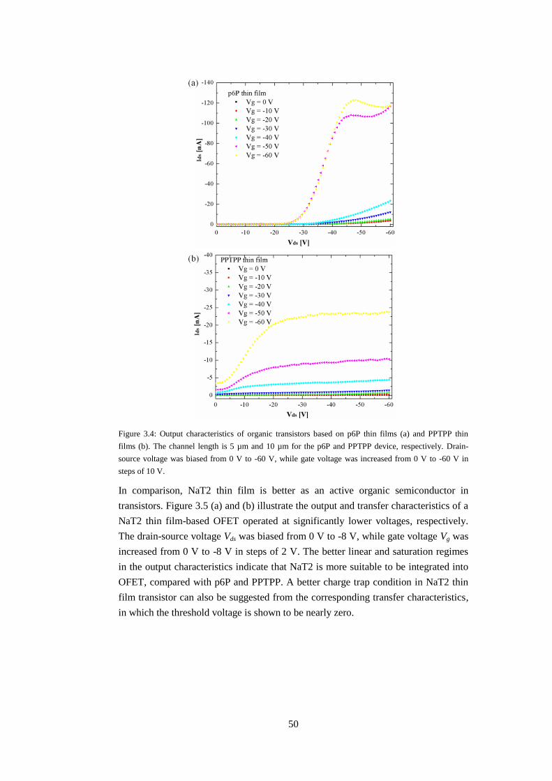
50
Figure 3.4: Output characteristics of organic transistors based on p6P thin films (a) and PPTPP thin
films (b). The channel length is 5 µm and 10 µm for the p6P and PPTPP device, respectively. Drain-
source voltage was biased from 0 V to -60 V, while gate voltage was increased from 0 V to -60 V in
steps of 10 V.
In comparison, NaT2 thin film is better as an active organic semiconductor in
transistors. Figure 3.5 (a) and (b) illustrate the output and transfer characteristics of a
NaT2 thin film-based OFET operated at significantly lower voltages, respectively.
The drain-source voltage Vds was biased from 0 V to -8 V, while gate voltage Vg was
increased from 0 V to -8 V in steps of 2 V. The better linear and saturation regimes
in the output characteristics indicate that NaT2 is more suitable to be integrated into
OFET, compared with p6P and PPTPP. A better charge trap condition in NaT2 thin
film transistor can also be suggested from the corresponding transfer characteristics,
in which the threshold voltage is shown to be nearly zero.
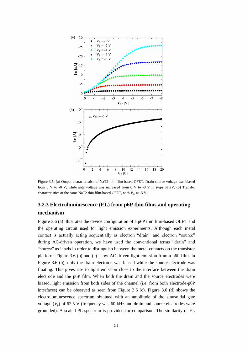
51
Figure 3.5: (a) Output characteristics of NaT2 thin film-based OFET. Drain-source voltage was biased
from 0 V to -8 V, while gate voltage was increased from 0 V to -8 V in steps of 2V. (b) Transfer
characteristics of the same NaT2 thin film-based OFET, with Vds at -5 V.
3.2.3 Electroluminescence (EL) from p6P thin films and operating
mechanism
Figure 3.6 (a) illustrates the device configuration of a p6P thin film-based OLET and
the operating circuit used for light emission experiments. Although each metal
contact is actually acting sequentially as electron “drain” and electron “source”
during AC-driven operation, we have used the conventional terms “drain” and
“source” as labels in order to distinguish between the metal contacts on the transistor
platform. Figure 3.6 (b) and (c) show AC-driven light emission from a p6P film. In
Figure 3.6 (b), only the drain electrode was biased while the source electrode was
floating. This gives rise to light emission close to the interface between the drain
electrode and the p6P film. When both the drain and the source electrodes were
biased, light emission from both sides of the channel (i.e. from both electrode-p6P
interfaces) can be observed as seen from Figure 3.6 (c). Figure 3.6 (d) shows the
electroluminescence spectrum obtained with an amplitude of the sinusoidal gate
voltage (Vp) of 62.5 V (frequency was 60 kHz and drain and source electrodes were
grounded). A scaled PL spectrum is provided for comparison. The similarity of EL
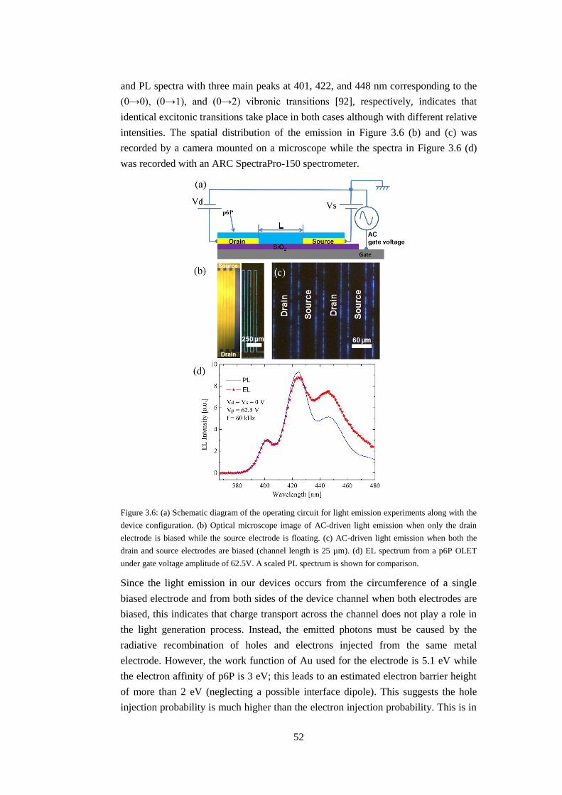
52
and PL spectra with three main peaks at 401, 422, and 448 nm corresponding to the
(0→0), (0→1), and (0→2) vibronic transitions [92], respectively, indicates that
identical excitonic transitions take place in both cases although with different relative
intensities. The spatial distribution of the emission in Figure 3.6 (b) and (c) was
recorded by a camera mounted on a microscope while the spectra in Figure 3.6 (d)
was recorded with an ARC SpectraPro-150 spectrometer.
Figure 3.6: (a) Schematic diagram of the operating circuit for light emission experiments along with the
device configuration. (b) Optical microscope image of AC-driven light emission when only the drain
electrode is biased while the source electrode is floating. (c) AC-driven light emission when both the
drain and source electrodes are biased (channel length is 25 µm). (d) EL spectrum from a p6P OLET
under gate voltage amplitude of 62.5V. A scaled PL spectrum is shown for comparison.
Since the light emission in our devices occurs from the circumference of a single
biased electrode and from both sides of the device channel when both electrodes are
biased, this indicates that charge transport across the channel does not play a role in
the light generation process. Instead, the emitted photons must be caused by the
radiative recombination of holes and electrons injected from the same metal
electrode. However, the work function of Au used for the electrode is 5.1 eV while
the electron affinity of p6P is 3 eV; this leads to an estimated electron barrier height
of more than 2 eV (neglecting a possible interface dipole). This suggests the hole
injection probability is much higher than the electron injection probability. This is in
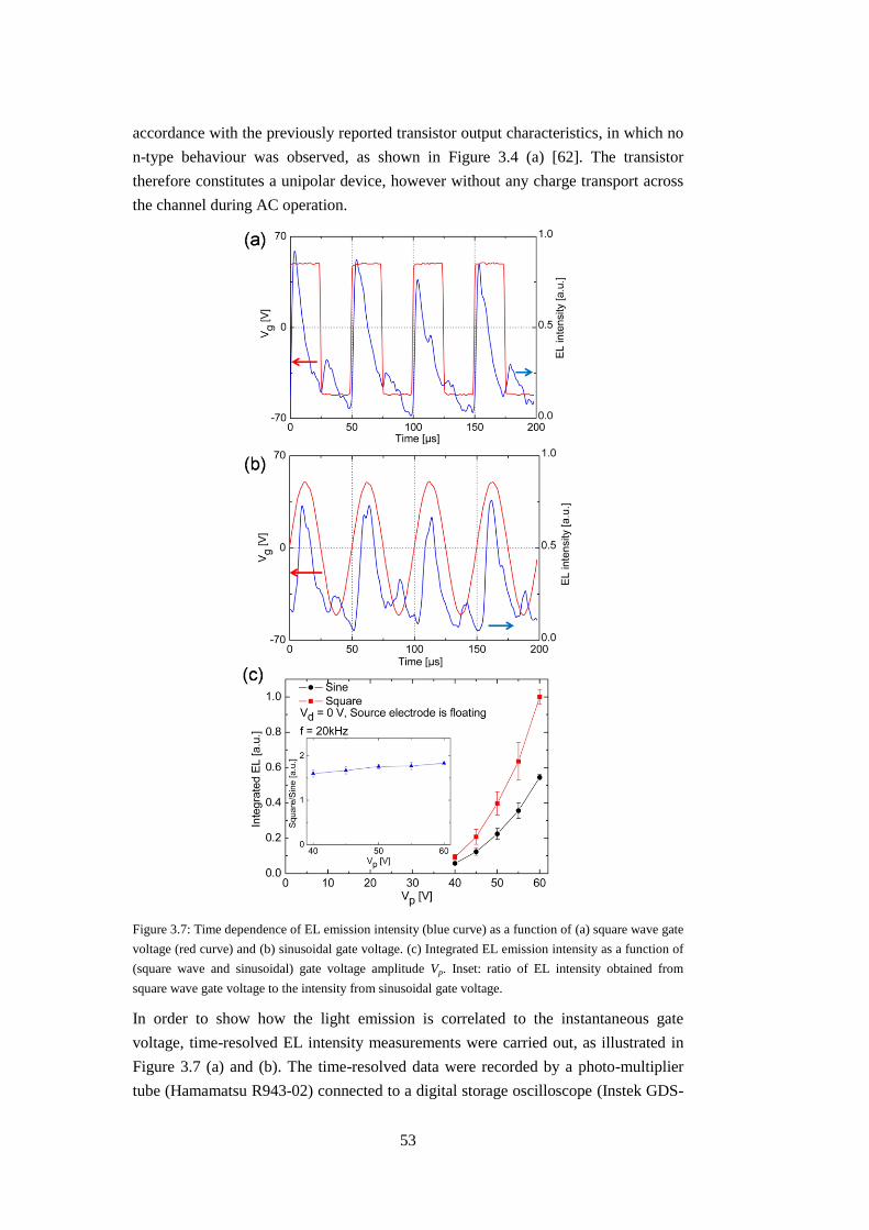
53
accordance with the previously reported transistor output characteristics, in which no
n-type behaviour was observed, as shown in Figure 3.4 (a) [62]. The transistor
therefore constitutes a unipolar device, however without any charge transport across
the channel during AC operation.
Figure 3.7: Time dependence of EL emission intensity (blue curve) as a function of (a) square wave gate
voltage (red curve) and (b) sinusoidal gate voltage. (c) Integrated EL emission intensity as a function of
(square wave and sinusoidal) gate voltage amplitude Vp. Inset: ratio of EL intensity obtained from
square wave gate voltage to the intensity from sinusoidal gate voltage.
In order to show how the light emission is correlated to the instantaneous gate
voltage, time-resolved EL intensity measurements were carried out, as illustrated in
Figure 3.7 (a) and (b). The time-resolved data were recorded by a photo-multiplier
tube (Hamamatsu R943-02) connected to a digital storage oscilloscope (Instek GDS-
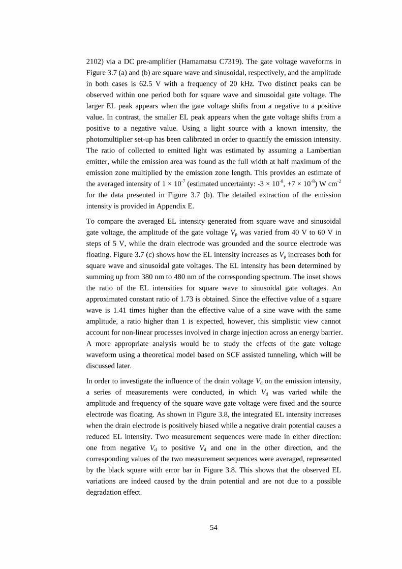
54
2102) via a DC pre-amplifier (Hamamatsu C7319). The gate voltage waveforms in
Figure 3.7 (a) and (b) are square wave and sinusoidal, respectively, and the amplitude
in both cases is 62.5 V with a frequency of 20 kHz. Two distinct peaks can be
observed within one period both for square wave and sinusoidal gate voltage. The
larger EL peak appears when the gate voltage shifts from a negative to a positive
value. In contrast, the smaller EL peak appears when the gate voltage shifts from a
positive to a negative value. Using a light source with a known intensity, the
photomultiplier set-up has been calibrated in order to quantify the emission intensity.
The ratio of collected to emitted light was estimated by assuming a Lambertian
emitter, while the emission area was found as the full width at half maximum of the
emission zone multiplied by the emission zone length. This provides an estimate of
the averaged intensity of 1 × 10⁻⁷
(estimated uncertainty: -3 × 10⁻⁸
, +7 × 10⁻⁸
) W cm-2
for the data presented in Figure 3.7 (b). The detailed extraction of the emission
intensity is provided in Appendix E.
To compare the averaged EL intensity generated from square wave and sinusoidal
gate voltage, the amplitude of the gate voltage Vp was varied from 40 V to 60 V in
steps of 5 V, while the drain electrode was grounded and the source electrode was
floating. Figure 3.7 (c) shows how the EL intensity increases as Vp increases both for
square wave and sinusoidal gate voltages. The EL intensity has been determined by
summing up from 380 nm to 480 nm of the corresponding spectrum. The inset shows
the ratio of the EL intensities for square wave to sinusoidal gate voltages. An
approximated constant ratio of 1.73 is obtained. Since the effective value of a square
wave is 1.41 times higher than the effective value of a sine wave with the same
amplitude, a ratio higher than 1 is expected, however, this simplistic view cannot
account for non-linear processes involved in charge injection across an energy barrier.
A more appropriate analysis would be to study the effects of the gate voltage
waveform using a theoretical model based on SCF assisted tunneling, which will be
discussed later.
In order to investigate the influence of the drain voltage Vd on the emission intensity,
a series of measurements were conducted, in which Vd was varied while the
amplitude and frequency of the square wave gate voltage were fixed and the source
electrode was floating. As shown in Figure 3.8, the integrated EL intensity increases
when the drain electrode is positively biased while a negative drain potential causes a
reduced EL intensity. Two measurement sequences were made in either direction:
one from negative Vd to positive Vd and one in the other direction, and the
corresponding values of the two measurement sequences were averaged, represented
by the black square with error bar in Figure 3.8. This shows that the observed EL
variations are indeed caused by the drain potential and are not due to a possible
degradation effect.
55
Figure 3.8: Integrated EL intensity as a function of drain electrode voltage Vd (source electrode was
floating). The gate voltage amplitude was Vp = 45 V and the frequency was f = 20 kHz.
On the basis of the experiments presented before, an operating mechanism of the
AC-driven OLET is proposed: Charge transport across the channel is not part of the
light generation process. Rather, the two types of charge-carriers are sequentially
injected from the same contact. This must mean that one type of charge is piled up in
the organic film close to the electrode interface during one half-period of the gate
voltage effectively forming a space-charge region at this position. During the
subsequent half-period of the gate voltage, the opposite charge-carrier is injected,
recombines with the first type of carrier, and thereby causes light emission. Since the
injection of holes is much more probable than the injection of electrons in our device,
the space-charge region must be formed by holes piling up either due to deep hole
traps or short hole transport distance under high frequency operation. The positive
space-charge region is therefore formed during the negative half-period of the gate
voltage, as illustrated in Figure 3.9 (a).
In the next (positive) half-period, electrons are injected into the organic material to
recombine with the previously injected holes. Since the injection barrier of electrons
between Au and p6P is very high, the electrons are most likely to tunnel into the p6P.
The electron tunneling process is primarily influenced by the positive space-charge
region rather than the positive gate voltage, as shown in Figure 3.9 (b). This can be
argued as follows: During the negative half-period of the gate voltage, holes are
injected. If the DC potential of the drain electrode is increased (positive Vd), this
leads to an increased hole injection and therefore a larger space-charge. In the
following, positive half-period of the gate voltage, electrons are tunneling into the
organic material. The positive value of Vd means that the drain to gate voltage
difference is effectively reduced. If the main factor driving the electron tunneling
would be the gate voltage, then the electron tunneling and thus also the emission
intensity should be less than at zero Vd. On the contrary, if the main driving
mechanism for electron injection is tunneling assisted by the positive space-charge
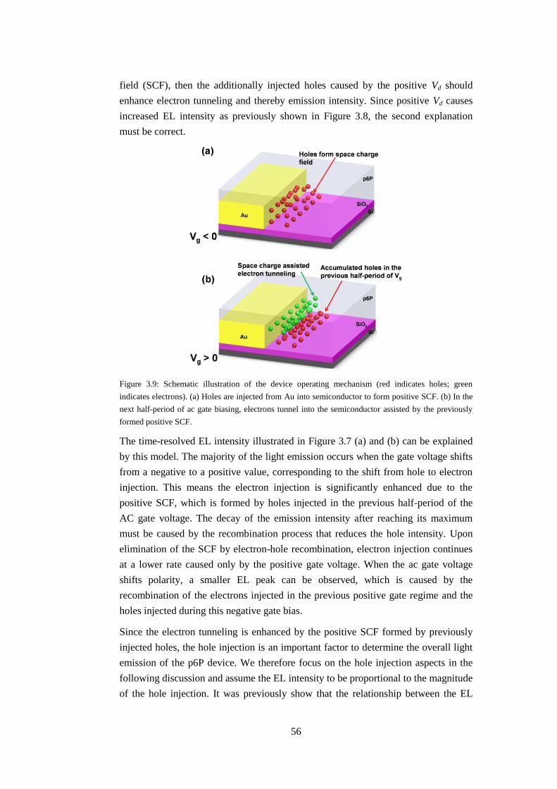
56
field (SCF), then the additionally injected holes caused by the positive Vd should
enhance electron tunneling and thereby emission intensity. Since positive Vd causes
increased EL intensity as previously shown in Figure 3.8, the second explanation
must be correct.
Figure 3.9: Schematic illustration of the device operating mechanism (red indicates holes; green
indicates electrons). (a) Holes are injected from Au into semiconductor to form positive SCF. (b) In the
next half-period of ac gate biasing, electrons tunnel into the semiconductor assisted by the previously
formed positive SCF.
The time-resolved EL intensity illustrated in Figure 3.7 (a) and (b) can be explained
by this model. The majority of the light emission occurs when the gate voltage shifts
from a negative to a positive value, corresponding to the shift from hole to electron
injection. This means the electron injection is significantly enhanced due to the
positive SCF, which is formed by holes injected in the previous half-period of the
AC gate voltage. The decay of the emission intensity after reaching its maximum
must be caused by the recombination process that reduces the hole intensity. Upon
elimination of the SCF by electron-hole recombination, electron injection continues
at a lower rate caused only by the positive gate voltage. When the ac gate voltage
shifts polarity, a smaller EL peak can be observed, which is caused by the
recombination of the electrons injected in the previous positive gate regime and the
holes injected during this negative gate bias.
Since the electron tunneling is enhanced by the positive SCF formed by previously
injected holes, the hole injection is an important factor to determine the overall light
emission of the p6P device. We therefore focus on the hole injection aspects in the
following discussion and assume the EL intensity to be proportional to the magnitude
of the hole injection. It was previously show that the relationship between the EL
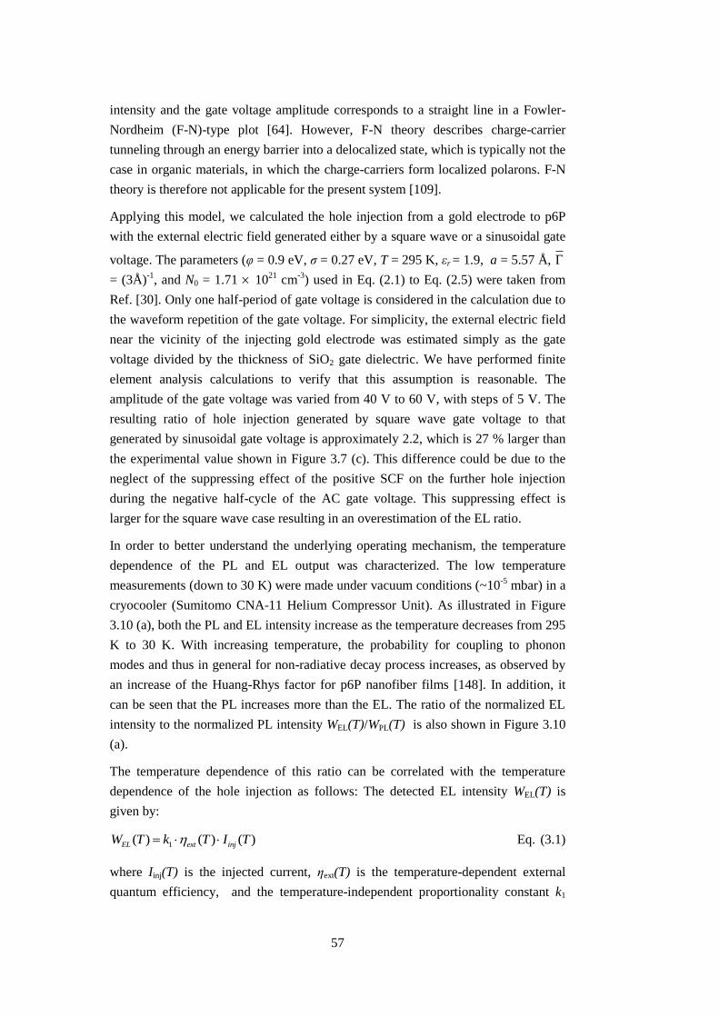
57
intensity and the gate voltage amplitude corresponds to a straight line in a Fowler-
Nordheim (F-N)-type plot [64]. However, F-N theory describes charge-carrier
tunneling through an energy barrier into a delocalized state, which is typically not the
case in organic materials, in which the charge-carriers form localized polarons. F-N
theory is therefore not applicable for the present system [109].
Applying this model, we calculated the hole injection from a gold electrode to p6P
with the external electric field generated either by a square wave or a sinusoidal gate
voltage. The parameters (φ = 0.9 eV, σ = 0.27 eV, T = 295 K, εr = 1.9, a = 5.57 Å,
= (3Å)-1
, and N0 = 1.71 1021
cm-3
) used in Eq. (2.1) to Eq. (2.5) were taken from
Ref. [30]. Only one half-period of gate voltage is considered in the calculation due to
the waveform repetition of the gate voltage. For simplicity, the external electric field
near the vicinity of the injecting gold electrode was estimated simply as the gate
voltage divided by the thickness of SiO2 gate dielectric. We have performed finite
element analysis calculations to verify that this assumption is reasonable. The
amplitude of the gate voltage was varied from 40 V to 60 V, with steps of 5 V. The
resulting ratio of hole injection generated by square wave gate voltage to that
generated by sinusoidal gate voltage is approximately 2.2, which is 27 % larger than
the experimental value shown in Figure 3.7 (c). This difference could be due to the
neglect of the suppressing effect of the positive SCF on the further hole injection
during the negative half-cycle of the AC gate voltage. This suppressing effect is
larger for the square wave case resulting in an overestimation of the EL ratio.
In order to better understand the underlying operating mechanism, the temperature
dependence of the PL and EL output was characterized. The low temperature
measurements (down to 30 K) were made under vacuum conditions (~10-5
mbar) in a
cryocooler (Sumitomo CNA-11 Helium Compressor Unit). As illustrated in Figure
3.10 (a), both the PL and EL intensity increase as the temperature decreases from 295
K to 30 K. With increasing temperature, the probability for coupling to phonon
modes and thus in general for non-radiative decay process increases, as observed by
an increase of the Huang-Rhys factor for p6P nanofiber films [148]. In addition, it
can be seen that the PL increases more than the EL. The ratio of the normalized EL
intensity to the normalized PL intensity WEL(T)/WPL(T) is also shown in Figure 3.10
(a).
The temperature dependence of this ratio can be correlated with the temperature
dependence of the hole injection as follows: The detected EL intensity WEL(T) is
given by:
1( ) ( ) ( )EL ext injW T k T I T Eq. (3.1)
where Iinj(T) is the injected current, ηext(T) is the temperature-dependent external
quantum efficiency, and the temperature-independent proportionality constant k1
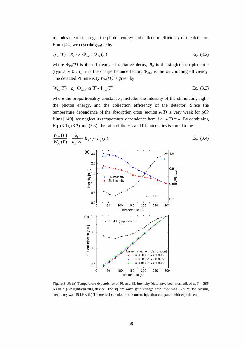
58
includes the unit charge, the photon energy and collection efficiency of the detector.
From [44] we describe ηext(T) by:
( ) ( )ext st outc PLT R T Eq. (3.2)
where ΦPL(T) is the efficiency of radiative decay, Rst is the singlet to triplet ratio
(typically 0.25), γ is the charge balance factor, Φoutc is the outcoupling efficiency.
The detected PL intensity WPL(T) is given by:
2( ) ( ) ( )PL outc PLW T k T T Eq. (3.3)
where the proportionality constant k2 includes the intensity of the stimulating light,
the photon energy, and the collection efficiency of the detector. Since the
temperature dependence of the absorption cross section α(T) is very weak for p6P
films [149], we neglect its temperature dependence here, i.e. α(T) = α. By combining
Eq. (3.1), (3.2) and (3.3), the ratio of the EL and PL intensities is found to be
1
2
( )( ).
( )
ELst inj
PL
W T kR I T
W T k
Eq. (3.4)
Figure 3.10: (a) Temperature dependence of PL and EL intensity (data have been normalized at T = 295
K) of a p6P light-emitting device. The square wave gate voltage amplitude was 37.5 V; the biasing
frequency was 15 kHz. (b) Theoretical calculation of current injection compared with experiment.
59
Since all factors in Eq. (3.4) except the injected current have negligible temperature
dependence, the ratio WEL(T)/WPL(T) should therefore have the same temperature
dependence as the injected current.
Figure 3.10 (b) shows the temperature dependence of the current injection calculated
using the approach based on Arkhipov’s model (see Section 2.1.2), and the ratio
derived from experiment is again illustrated for comparison. The calculated current
injection varies only slightly if the hole injection barrier or the energy width σ is
varied. Also, it can be seen that the theory predicts a stronger temperature
dependence than what is observed experimentally. This large deviation could be due
to the inadequacy of the Gaussian energy distribution of the hopping state [150].
Nevertheless, the calculation based on Arkhipov’s model reproduces qualitatively the
trend observed experimentally, which is not captured by the F-N formalism.
We have focused on the hole injection between gold and p6P because the hole
injection barrier in this case (typically 0.9 eV) is much lower than the electron
injection barrier (2.1 eV). In contrast, electron injection should be mainly studied for
the organic materials which possesses lower electron injection barrier with respect to
the injecting electrodes.
To rule out the possibility that impact ionization could be involved in the light
generation process, similar substrates but with aluminum rather than gold electrodes
were fabricated. Since aluminum electrodes oxidize under ambient conditions, there
will be an insulating layer of aluminum oxide between the electrode and the p6P, and
light emission would under such circumstances only be possible via impact
ionization [151]. Based on the sensitivity of our detection system, we estimate that
the light emission from aluminum electrode devices is at least two orders of
magnitude lower than that from gold electrode devices under similar biasing
parameters, indicating that impact ionization plays an insignificant role for the light
generation.
3.2.4 Self-assembled monolayer (SAM) modification
As described in Section 2.1.1, SAMs can be applied to modify the metal electrodes in
order to facilitate the charge carrier injection. ODT (powder, 286.57g/mol) and
PFDT (liquid, 480.18g/mol) were purchased from Aldrich and used without further
purification. The micro-scale substrates with Au electrode were separated into two
groups and rinsed in pure ethanol and 2-propanol, and blown dry with N2. The two
groups of substrates were subsequently immersed into ethanol solutions of ODT
(10mg/20ml, i.e., 1.75 mM) and PFDT (0.011ml/20ml, i.e., 1.75 mM), respectively,
for at least 16 hours. After the assembly process, the substrates were immediately
rinsed in pure ethanol and 2-propanol, and dried with N2 before the deposition of
PPTPP or p6P thin films.
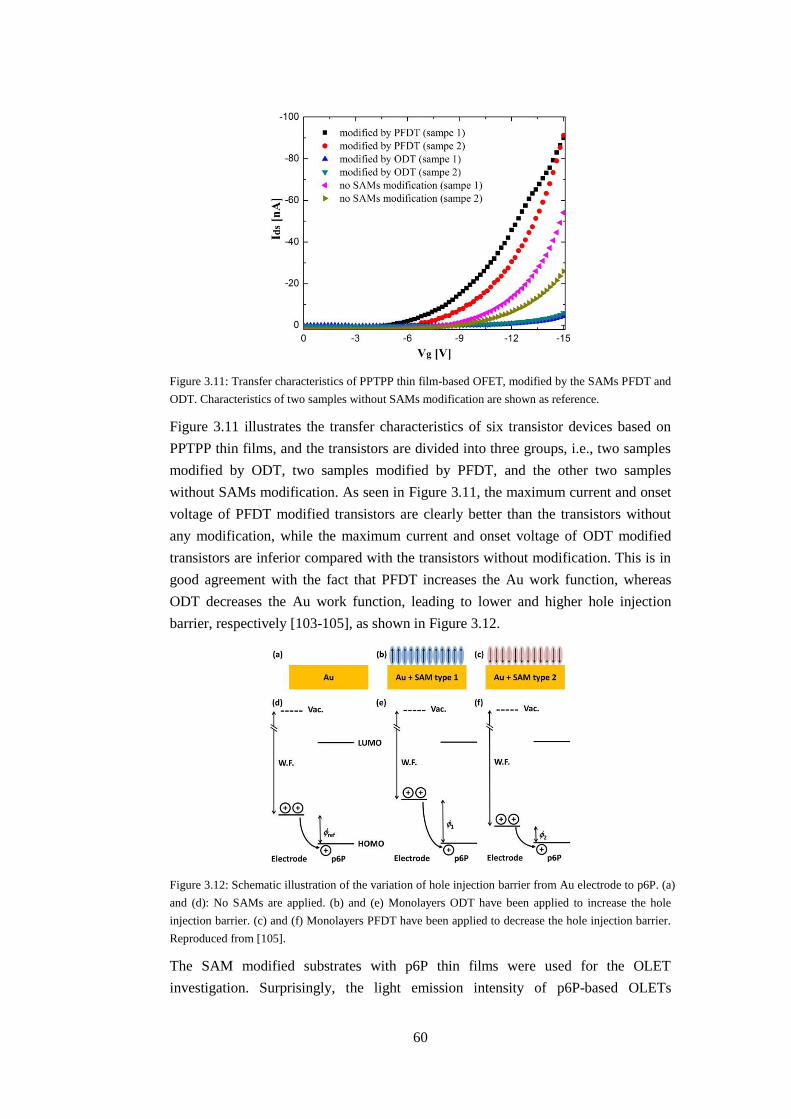
60
Figure 3.11: Transfer characteristics of PPTPP thin film-based OFET, modified by the SAMs PFDT and
ODT. Characteristics of two samples without SAMs modification are shown as reference.
Figure 3.11 illustrates the transfer characteristics of six transistor devices based on
PPTPP thin films, and the transistors are divided into three groups, i.e., two samples
modified by ODT, two samples modified by PFDT, and the other two samples
without SAMs modification. As seen in Figure 3.11, the maximum current and onset
voltage of PFDT modified transistors are clearly better than the transistors without
any modification, while the maximum current and onset voltage of ODT modified
transistors are inferior compared with the transistors without modification. This is in
good agreement with the fact that PFDT increases the Au work function, whereas
ODT decreases the Au work function, leading to lower and higher hole injection
barrier, respectively [103-105], as shown in Figure 3.12.
Figure 3.12: Schematic illustration of the variation of hole injection barrier from Au electrode to p6P. (a)
and (d): No SAMs are applied. (b) and (e) Monolayers ODT have been applied to increase the hole
injection barrier. (c) and (f) Monolayers PFDT have been applied to decrease the hole injection barrier.
Reproduced from [105].
The SAM modified substrates with p6P thin films were used for the OLET
investigation. Surprisingly, the light emission intensity of p6P-based OLETs
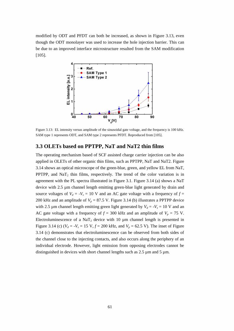
61
modified by ODT and PFDT can both be increased, as shown in Figure 3.13, even
though the ODT monolayer was used to increase the hole injection barrier. This can
be due to an improved interface microstructure resulted from the SAM modification
[105].
Figure 3.13: EL intensity versus amplitude of the sinusoidal gate voltage, and the frequency is 100 kHz.
SAM type 1 represents ODT, and SAM type 2 represents PFDT. Reproduced from [105].
3.3 OLETs based on PPTPP, NaT and NaT2 thin films
The operating mechanism based of SCF assisted charge carrier injection can be also
applied in OLETs of other organic thin films, such as PPTPP, NaT and NaT2. Figure
3.14 shows an optical microscope of the green-blue, green, and yellow EL from NaT,
PPTPP, and NaT2 thin films, respectively. The trend of the color variation is in
agreement with the PL spectra illustrated in Figure 3.1. Figure 3.14 (a) shows a NaT
device with 2.5 µm channel length emitting green-blue light generated by drain and
source voltages of Vd = -Vs = 10 V and an AC gate voltage with a frequency of f =
200 kHz and an amplitude of Vp = 87.5 V. Figure 3.14 (b) illustrates a PPTPP device
with 2.5 µm channel length emitting green light generated by Vd = -Vs = 10 V and an
AC gate voltage with a frequency of f = 300 kHz and an amplitude of Vp = 75 V.
Electroluminescence of a NaT2 device with 10 µm channel length is presented in
Figure 3.14 (c) (Vd = -Vs = 15 V, f = 200 kHz, and Vp = 62.5 V). The inset of Figure
3.14 (c) demonstrates that electroluminescence can be observed from both sides of
the channel close to the injecting contacts, and also occurs along the periphery of an
individual electrode. However, light emission from opposing electrodes cannot be
distinguished in devices with short channel lengths such as 2.5 µm and 5 µm.
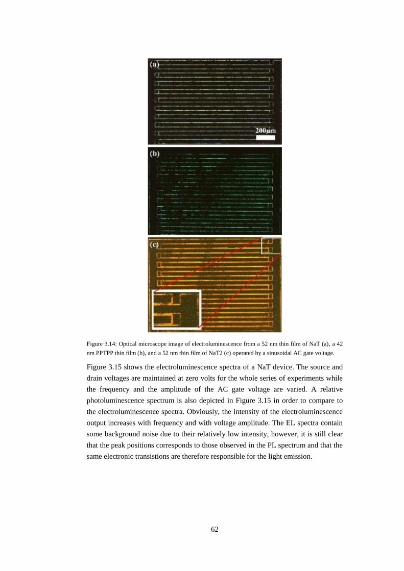
62
Figure 3.14: Optical microscope image of electroluminescence from a 52 nm thin film of NaT (a), a 42
nm PPTPP thin film (b), and a 52 nm thin film of NaT2 (c) operated by a sinusoidal AC gate voltage.
Figure 3.15 shows the electroluminescence spectra of a NaT device. The source and
drain voltages are maintained at zero volts for the whole series of experiments while
the frequency and the amplitude of the AC gate voltage are varied. A relative
photoluminescence spectrum is also depicted in Figure 3.15 in order to compare to
the electroluminescence spectra. Obviously, the intensity of the electroluminescence
output increases with frequency and with voltage amplitude. The EL spectra contain
some background noise due to their relatively low intensity, however, it is still clear
that the peak positions corresponds to those observed in the PL spectrum and that the
same electronic transistions are therefore responsible for the light emission.
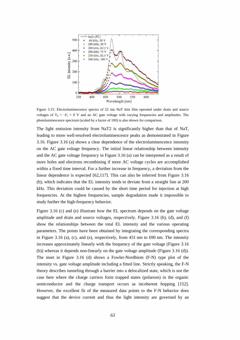
63
Figure 3.15: Electroluminescence spectra of 52 nm NaT thin film operated under drain and source
voltages of Vd = -Vs = 0 V and an AC gate voltage with varying frequencies and amplitudes. The
photoluminescence spectrum (scaled by a factor of 100) is also shown for comparison.
The light emission intensity from NaT2 is significantly higher than that of NaT,
leading to more well-resolved electroluminescence peaks as demonstrated in Figure
3.16. Figure 3.16 (a) shows a clear dependence of the electroluminescence intensity
on the AC gate voltage frequency. The initial linear relationship between intensity
and the AC gate voltage frequency in Figure 3.16 (a) can be interpreted as a result of
more holes and electrons recombining if more AC voltage cycles are accomplished
within a fixed time interval. For a further increase in frequency, a deviation from the
linear dependence is expected [62,117]. This can also be inferred from Figure 3.16
(b), which indicates that the EL intensity tends to deviate from a straight line at 200
kHz. This deviation could be caused by the short time period for injection at high
frequencies. At the highest frequencies, sample degradation made it impossible to
study further the high-frequency behavior.
Figure 3.16 (c) and (e) illustrate how the EL spectrum depends on the gate voltage
amplitude and drain and source voltages, respectively. Figure 3.16 (b), (d), and (f)
show the relationships between the total EL intensity and the various operating
parameters. The points have been obtained by integrating the corresponding spectra
in Figure 3.16 (a), (c), and (e), respectively, from 431 nm to 690 nm. The intensity
increases approximately linearly with the frequency of the gate voltage (Figure 3.16
(b)) whereas it depends non-linearly on the gate voltage amplitude (Figure 3.16 (d)).
The inset in Figure 3.16 (d) shows a Fowler-Nordhiem (F-N) type plot of the
intensity vs. gate voltage amplitude including a fitted line. Strictly speaking, the F-N
theory describes tunneling through a barrier into a delocalized state, which is not the
case here where the charge carriers form trapped states (polarons) in the organic
semiconductor and the charge transport occurs as incoherent hopping [152].
However, the excellent fit of the measured data points to the F-N behavior does
suggest that the device current and thus the light intensity are governed by an
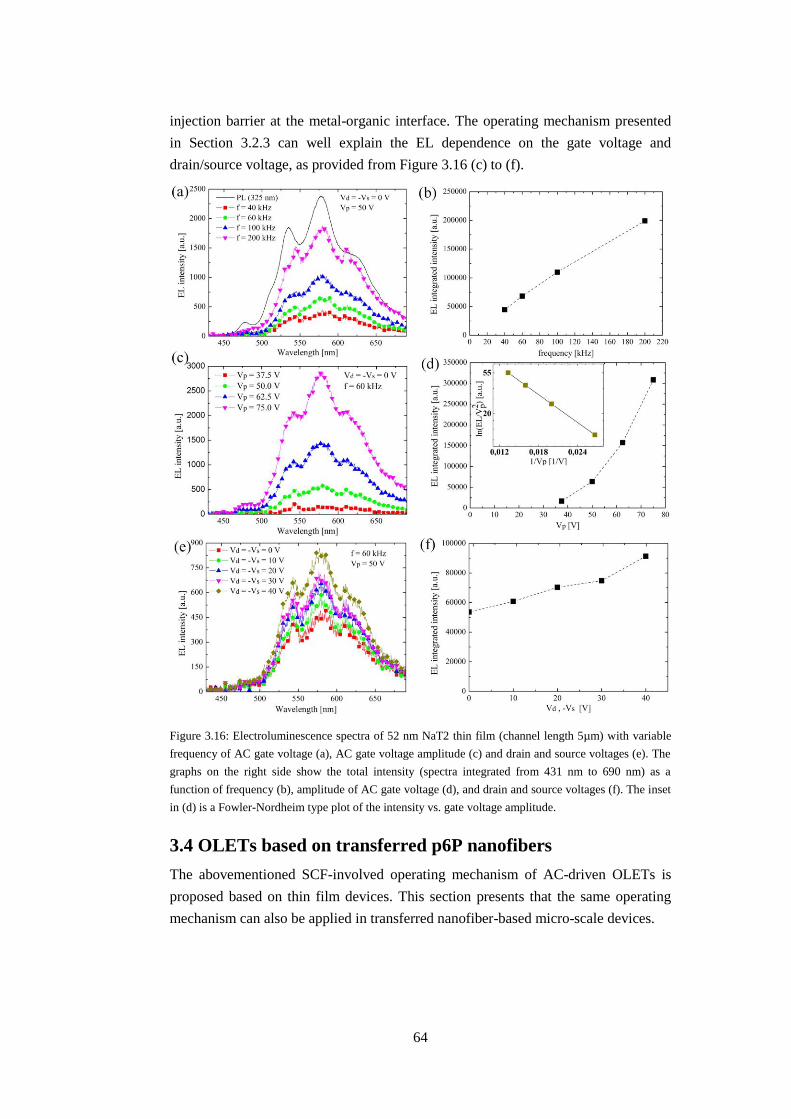
64
injection barrier at the metal-organic interface. The operating mechanism presented
in Section 3.2.3 can well explain the EL dependence on the gate voltage and
drain/source voltage, as provided from Figure 3.16 (c) to (f).
Figure 3.16: Electroluminescence spectra of 52 nm NaT2 thin film (channel length 5µm) with variable
frequency of AC gate voltage (a), AC gate voltage amplitude (c) and drain and source voltages (e). The
graphs on the right side show the total intensity (spectra integrated from 431 nm to 690 nm) as a
function of frequency (b), amplitude of AC gate voltage (d), and drain and source voltages (f). The inset
in (d) is a Fowler-Nordheim type plot of the intensity vs. gate voltage amplitude.
3.4 OLETs based on transferred p6P nanofibers
The abovementioned SCF-involved operating mechanism of AC-driven OLETs is
proposed based on thin film devices. This section presents that the same operating
mechanism can also be applied in transferred nanofiber-based micro-scale devices.
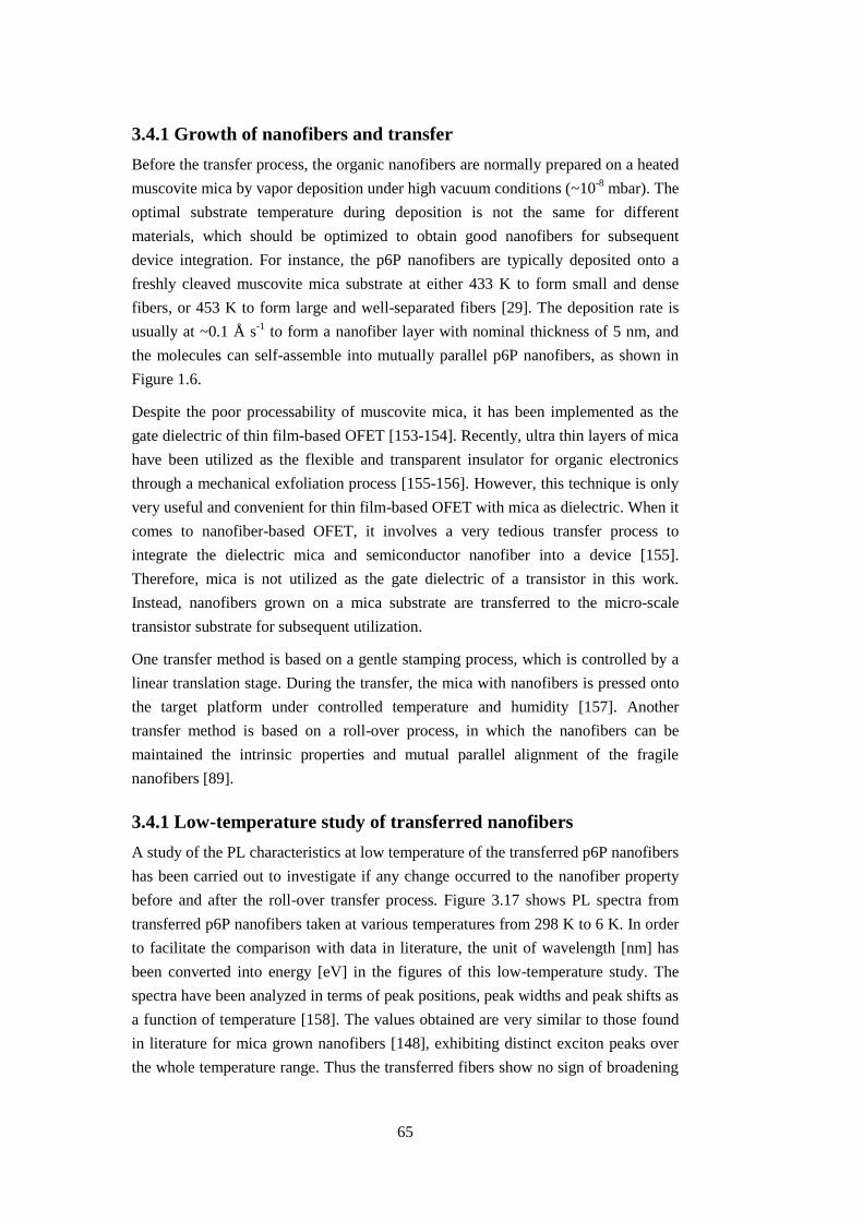
65
3.4.1 Growth of nanofibers and transfer
Before the transfer process, the organic nanofibers are normally prepared on a heated
muscovite mica by vapor deposition under high vacuum conditions (~10-8
mbar). The
optimal substrate temperature during deposition is not the same for different
materials, which should be optimized to obtain good nanofibers for subsequent
device integration. For instance, the p6P nanofibers are typically deposited onto a
freshly cleaved muscovite mica substrate at either 433 K to form small and dense
fibers, or 453 K to form large and well-separated fibers [29]. The deposition rate is
usually at ~0.1 Å s-1
to form a nanofiber layer with nominal thickness of 5 nm, and
the molecules can self-assemble into mutually parallel p6P nanofibers, as shown in
Figure 1.6.
Despite the poor processability of muscovite mica, it has been implemented as the
gate dielectric of thin film-based OFET [153-154]. Recently, ultra thin layers of mica
have been utilized as the flexible and transparent insulator for organic electronics
through a mechanical exfoliation process [155-156]. However, this technique is only
very useful and convenient for thin film-based OFET with mica as dielectric. When it
comes to nanofiber-based OFET, it involves a very tedious transfer process to
integrate the dielectric mica and semiconductor nanofiber into a device [155].
Therefore, mica is not utilized as the gate dielectric of a transistor in this work.
Instead, nanofibers grown on a mica substrate are transferred to the micro-scale
transistor substrate for subsequent utilization.
One transfer method is based on a gentle stamping process, which is controlled by a
linear translation stage. During the transfer, the mica with nanofibers is pressed onto
the target platform under controlled temperature and humidity [157]. Another
transfer method is based on a roll-over process, in which the nanofibers can be
maintained the intrinsic properties and mutual parallel alignment of the fragile
nanofibers [89].
3.4.1 Low-temperature study of transferred nanofibers
A study of the PL characteristics at low temperature of the transferred p6P nanofibers
has been carried out to investigate if any change occurred to the nanofiber property
before and after the roll-over transfer process. Figure 3.17 shows PL spectra from
transferred p6P nanofibers taken at various temperatures from 298 K to 6 K. In order
to facilitate the comparison with data in literature, the unit of wavelength [nm] has
been converted into energy [eV] in the figures of this low-temperature study. The
spectra have been analyzed in terms of peak positions, peak widths and peak shifts as
a function of temperature [158]. The values obtained are very similar to those found
in literature for mica grown nanofibers [148], exhibiting distinct exciton peaks over
the whole temperature range. Thus the transferred fibers show no sign of broadening
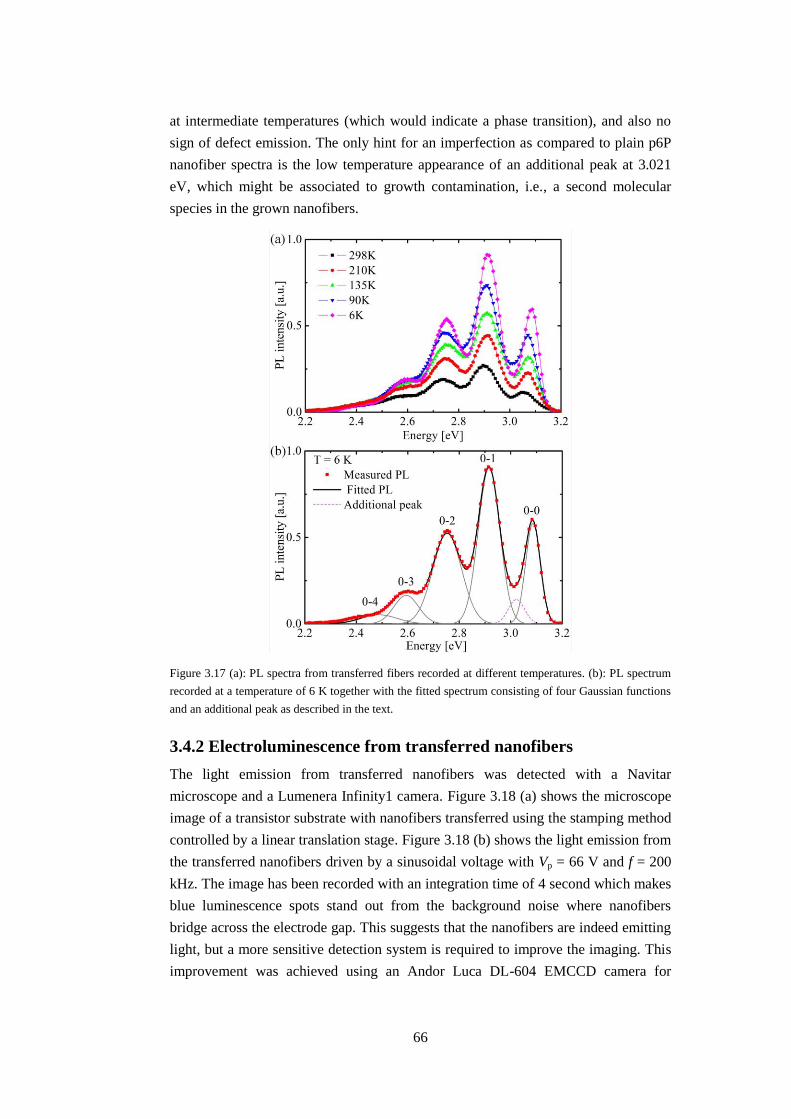
66
at intermediate temperatures (which would indicate a phase transition), and also no
sign of defect emission. The only hint for an imperfection as compared to plain p6P
nanofiber spectra is the low temperature appearance of an additional peak at 3.021
eV, which might be associated to growth contamination, i.e., a second molecular
species in the grown nanofibers.
Figure 3.17 (a): PL spectra from transferred fibers recorded at different temperatures. (b): PL spectrum
recorded at a temperature of 6 K together with the fitted spectrum consisting of four Gaussian functions
and an additional peak as described in the text.
3.4.2 Electroluminescence from transferred nanofibers
The light emission from transferred nanofibers was detected with a Navitar
microscope and a Lumenera Infinity1 camera. Figure 3.18 (a) shows the microscope
image of a transistor substrate with nanofibers transferred using the stamping method
controlled by a linear translation stage. Figure 3.18 (b) shows the light emission from
the transferred nanofibers driven by a sinusoidal voltage with Vp = 66 V and f = 200
kHz. The image has been recorded with an integration time of 4 second which makes
blue luminescence spots stand out from the background noise where nanofibers
bridge across the electrode gap. This suggests that the nanofibers are indeed emitting
light, but a more sensitive detection system is required to improve the imaging. This
improvement was achieved using an Andor Luca DL-604 EMCCD camera for
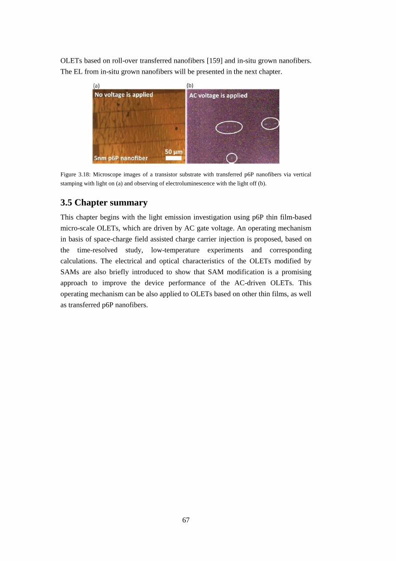
67
OLETs based on roll-over transferred nanofibers [159] and in-situ grown nanofibers.
The EL from in-situ grown nanofibers will be presented in the next chapter.
Figure 3.18: Microscope images of a transistor substrate with transferred p6P nanofibers via vertical
stamping with light on (a) and observing of electroluminescence with the light off (b).
3.5 Chapter summary
This chapter begins with the light emission investigation using p6P thin film-based
micro-scale OLETs, which are driven by AC gate voltage. An operating mechanism
in basis of space-charge field assisted charge carrier injection is proposed, based on
the time-resolved study, low-temperature experiments and corresponding
calculations. The electrical and optical characteristics of the OLETs modified by
SAMs are also briefly introduced to show that SAM modification is a promising
approach to improve the device performance of the AC-driven OLETs. This
operating mechanism can be also applied to OLETs based on other thin films, as well
as transferred p6P nanofibers.

68
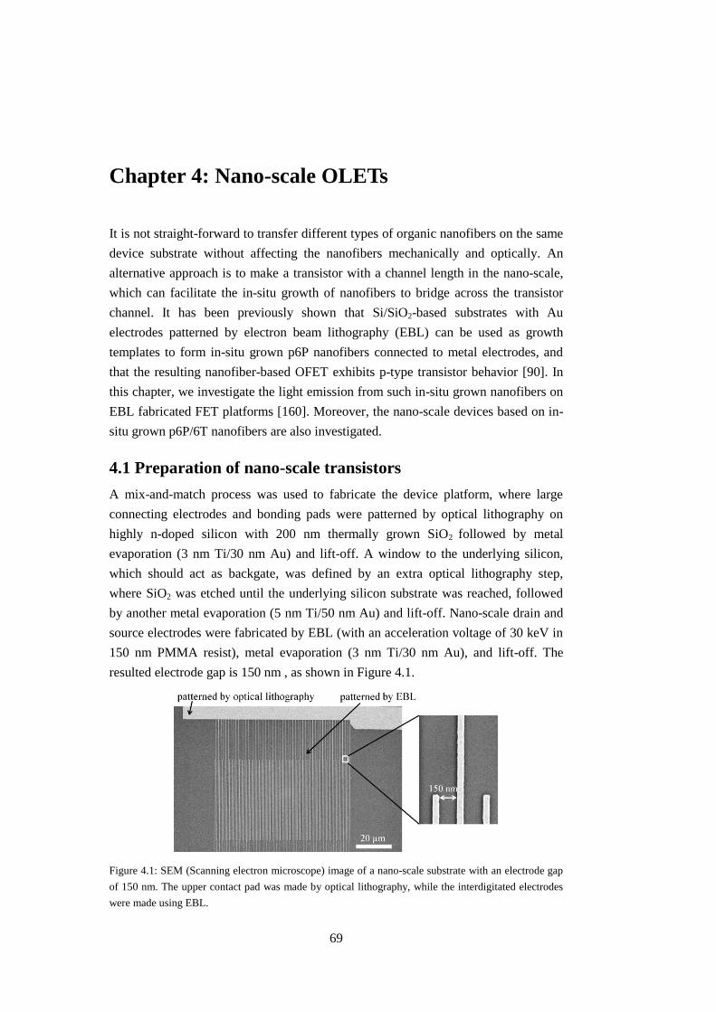
69
Chapter 4: Nano-scale OLETs
It is not straight-forward to transfer different types of organic nanofibers on the same
device substrate without affecting the nanofibers mechanically and optically. An
alternative approach is to make a transistor with a channel length in the nano-scale,
which can facilitate the in-situ growth of nanofibers to bridge across the transistor
channel. It has been previously shown that Si/SiO2-based substrates with Au
electrodes patterned by electron beam lithography (EBL) can be used as growth
templates to form in-situ grown p6P nanofibers connected to metal electrodes, and
that the resulting nanofiber-based OFET exhibits p-type transistor behavior [90]. In
this chapter, we investigate the light emission from such in-situ grown nanofibers on
EBL fabricated FET platforms [160]. Moreover, the nano-scale devices based on in-
situ grown p6P/6T nanofibers are also investigated.
4.1 Preparation of nano-scale transistors
A mix-and-match process was used to fabricate the device platform, where large
connecting electrodes and bonding pads were patterned by optical lithography on
highly n-doped silicon with 200 nm thermally grown SiO2 followed by metal
evaporation (3 nm Ti/30 nm Au) and lift-off. A window to the underlying silicon,
which should act as backgate, was defined by an extra optical lithography step,
where SiO2 was etched until the underlying silicon substrate was reached, followed
by another metal evaporation (5 nm Ti/50 nm Au) and lift-off. Nano-scale drain and
source electrodes were fabricated by EBL (with an acceleration voltage of 30 keV in
150 nm PMMA resist), metal evaporation (3 nm Ti/30 nm Au), and lift-off. The
resulted electrode gap is 150 nm , as shown in Figure 4.1.
Figure 4.1: SEM (Scanning electron microscope) image of a nano-scale substrate with an electrode gap
of 150 nm. The upper contact pad was made by optical lithography, while the interdigitated electrodes
were made using EBL.
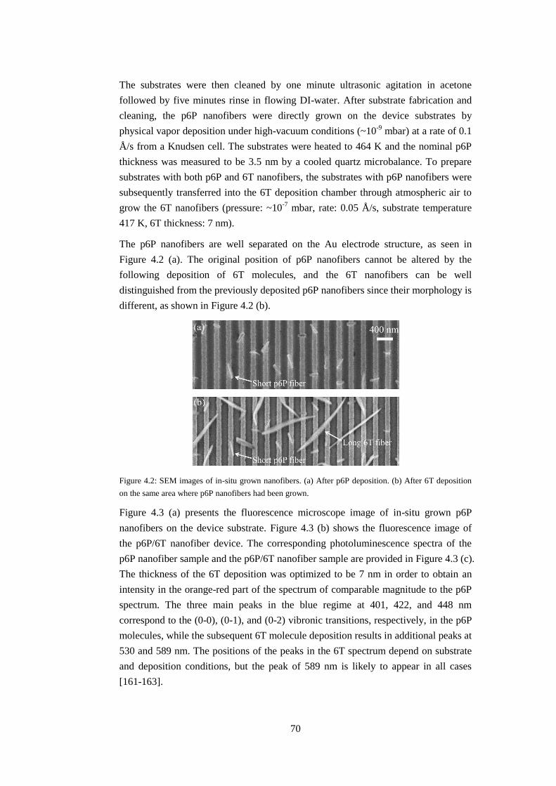
70
The substrates were then cleaned by one minute ultrasonic agitation in acetone
followed by five minutes rinse in flowing DI-water. After substrate fabrication and
cleaning, the p6P nanofibers were directly grown on the device substrates by
physical vapor deposition under high-vacuum conditions (~10-9
mbar) at a rate of 0.1
Å/s from a Knudsen cell. The substrates were heated to 464 K and the nominal p6P
thickness was measured to be 3.5 nm by a cooled quartz microbalance. To prepare
substrates with both p6P and 6T nanofibers, the substrates with p6P nanofibers were
subsequently transferred into the 6T deposition chamber through atmospheric air to
grow the 6T nanofibers (pressure: ~10-7
mbar, rate: 0.05 Å/s, substrate temperature
417 K, 6T thickness: 7 nm).
The p6P nanofibers are well separated on the Au electrode structure, as seen in
Figure 4.2 (a). The original position of p6P nanofibers cannot be altered by the
following deposition of 6T molecules, and the 6T nanofibers can be well
distinguished from the previously deposited p6P nanofibers since their morphology is
different, as shown in Figure 4.2 (b).
Figure 4.2: SEM images of in-situ grown nanofibers. (a) After p6P deposition. (b) After 6T deposition
on the same area where p6P nanofibers had been grown.
Figure 4.3 (a) presents the fluorescence microscope image of in-situ grown p6P
nanofibers on the device substrate. Figure 4.3 (b) shows the fluorescence image of
the p6P/6T nanofiber device. The corresponding photoluminescence spectra of the
p6P nanofiber sample and the p6P/6T nanofiber sample are provided in Figure 4.3 (c).
The thickness of the 6T deposition was optimized to be 7 nm in order to obtain an
intensity in the orange-red part of the spectrum of comparable magnitude to the p6P
spectrum. The three main peaks in the blue regime at 401, 422, and 448 nm
correspond to the (0-0), (0-1), and (0-2) vibronic transitions, respectively, in the p6P
molecules, while the subsequent 6T molecule deposition results in additional peaks at
530 and 589 nm. The positions of the peaks in the 6T spectrum depend on substrate
and deposition conditions, but the peak of 589 nm is likely to appear in all cases
[161-163].
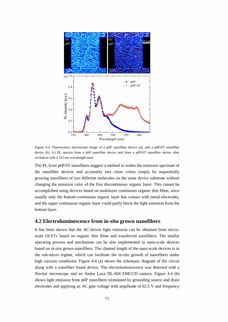
71
Figure 4.3: Fluorescence microscope image of a p6P nanofiber device (a), and a p6P/6T nanofiber
device (b). (c) PL spectra from a p6P nanofiber device and from a p6P/6T nanofiber device after
excitation with a 325 nm wavelength laser.
The PL from p6P/6T nanofibers suggest a method to widen the emission spectrum of
the nanofiber devices and accurately mix clean colors simply by sequentially
growing nanofibers of two different molecules on the same device substrate without
changing the emission color of the first discontinuous organic layer. This cannot be
accomplished using devices based on multilayer continuous organic thin films, since
usually only the bottom continuous organic layer has contact with metal electrodes,
and the upper continuous organic layer could partly block the light emission from the
bottom layer.
4.2 Electroluminescence from in-situ grown nanofibers
It has been shown that the AC-driven light emission can be obtained from micro-
scale OLETs based on organic thin films and transferred nanofibers. The similar
operating process and mechanism can be also implemented in nano-scale devices
based on in-situ grown nanofibers. The channel length of the nano-scale devices is in
the sub-micro regime, which can facilitate the in-situ growth of nanofibers under
high vacuum conditions. Figure 4.4 (a) shows the schematic diagram of the circuit
along with a nanofiber based device. The electroluminescence was detected with a
Navitar microscope and an Andor Luca DL-604 EMCCD camera. Figure 4.4 (b)
shows light emission from p6P nanofibers stimulated by grounding source and drain
electrodes and applying an AC gate voltage with amplitude of 62.5 V and frequency
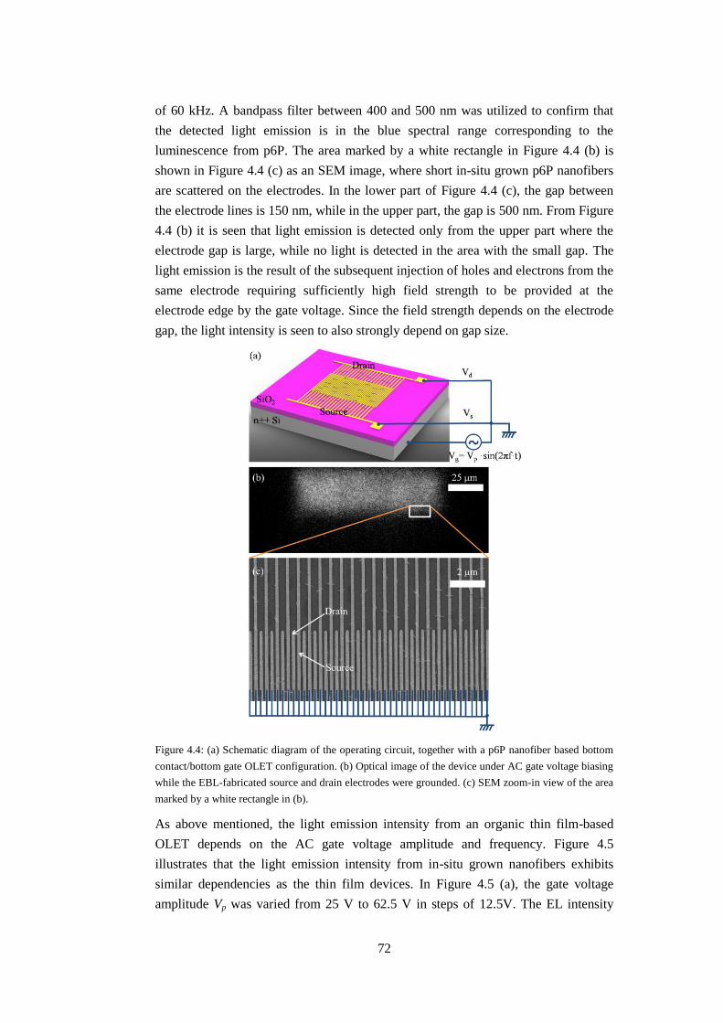
72
of 60 kHz. A bandpass filter between 400 and 500 nm was utilized to confirm that
the detected light emission is in the blue spectral range corresponding to the
luminescence from p6P. The area marked by a white rectangle in Figure 4.4 (b) is
shown in Figure 4.4 (c) as an SEM image, where short in-situ grown p6P nanofibers
are scattered on the electrodes. In the lower part of Figure 4.4 (c), the gap between
the electrode lines is 150 nm, while in the upper part, the gap is 500 nm. From Figure
4.4 (b) it is seen that light emission is detected only from the upper part where the
electrode gap is large, while no light is detected in the area with the small gap. The
light emission is the result of the subsequent injection of holes and electrons from the
same electrode requiring sufficiently high field strength to be provided at the
electrode edge by the gate voltage. Since the field strength depends on the electrode
gap, the light intensity is seen to also strongly depend on gap size.
Figure 4.4: (a) Schematic diagram of the operating circuit, together with a p6P nanofiber based bottom
contact/bottom gate OLET configuration. (b) Optical image of the device under AC gate voltage biasing
while the EBL-fabricated source and drain electrodes were grounded. (c) SEM zoom-in view of the area
marked by a white rectangle in (b).
As above mentioned, the light emission intensity from an organic thin film-based
OLET depends on the AC gate voltage amplitude and frequency. Figure 4.5
illustrates that the light emission intensity from in-situ grown nanofibers exhibits
similar dependencies as the thin film devices. In Figure 4.5 (a), the gate voltage
amplitude Vp was varied from 25 V to 62.5 V in steps of 12.5V. The EL intensity
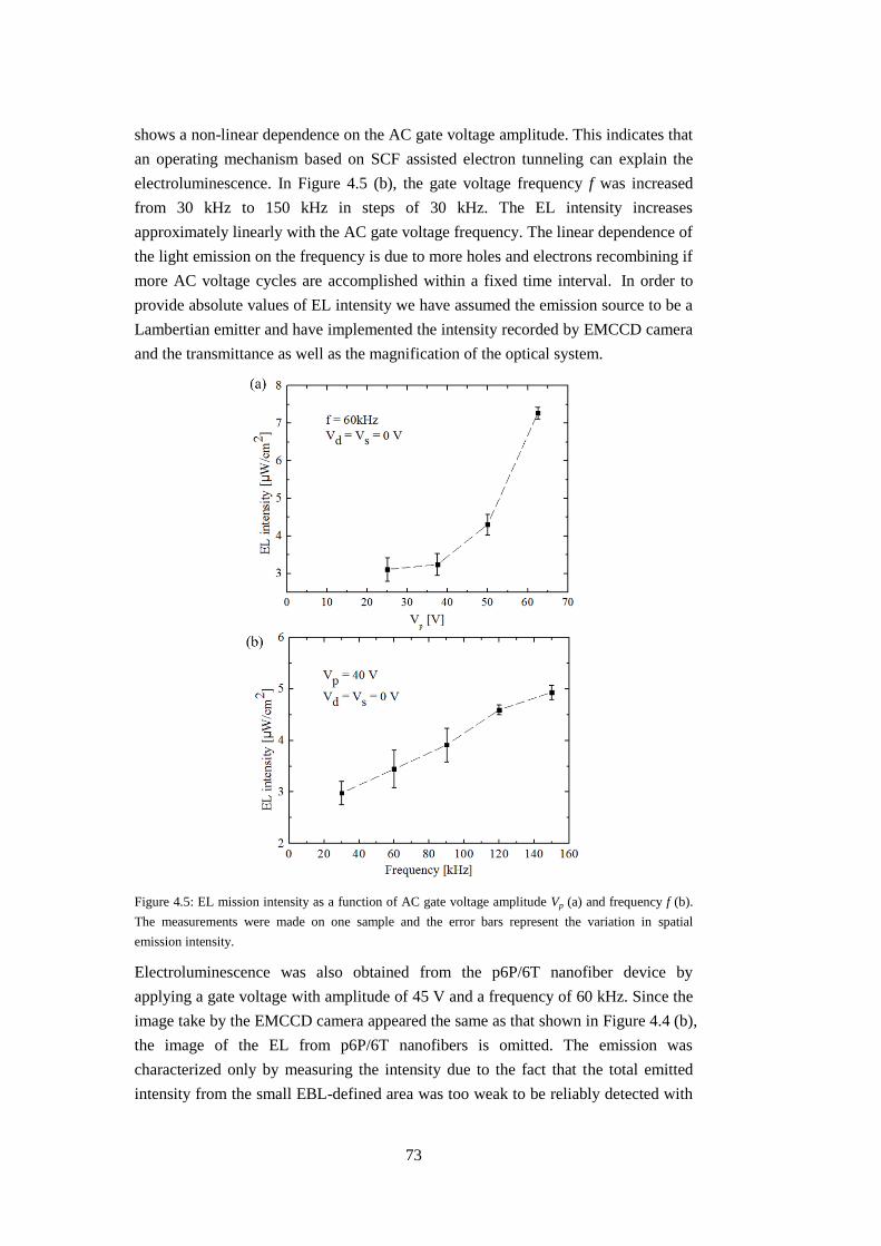
73
shows a non-linear dependence on the AC gate voltage amplitude. This indicates that
an operating mechanism based on SCF assisted electron tunneling can explain the
electroluminescence. In Figure 4.5 (b), the gate voltage frequency f was increased
from 30 kHz to 150 kHz in steps of 30 kHz. The EL intensity increases
approximately linearly with the AC gate voltage frequency. The linear dependence of
the light emission on the frequency is due to more holes and electrons recombining if
more AC voltage cycles are accomplished within a fixed time interval. In order to
provide absolute values of EL intensity we have assumed the emission source to be a
Lambertian emitter and have implemented the intensity recorded by EMCCD camera
and the transmittance as well as the magnification of the optical system.
Figure 4.5: EL mission intensity as a function of AC gate voltage amplitude Vp (a) and frequency f (b).
The measurements were made on one sample and the error bars represent the variation in spatial
emission intensity.
Electroluminescence was also obtained from the p6P/6T nanofiber device by
applying a gate voltage with amplitude of 45 V and a frequency of 60 kHz. Since the
image take by the EMCCD camera appeared the same as that shown in Figure 4.4 (b),
the image of the EL from p6P/6T nanofibers is omitted. The emission was
characterized only by measuring the intensity due to the fact that the total emitted
intensity from the small EBL-defined area was too weak to be reliably detected with
74
a spectrometer. Two intensity measurements were made, one of total emitted
intensity, and one in which a Thorlabs FEL 500 filter (longpass, cut-off wavelength
of 500 nm) was inserted into the optical path to detect the contribution from the 6T
nanofibers. The contribution of 6T nanofibers was quantified by extracting and
comparing the background-excluded signal from three different emission areas and it
turned out that the intensity above 500 nm corresponds to approx. 0.6 of the total
AC-driven light emission. As the spectrum in Figure 4.3 (c) shows, p6P has some
spectral content at wavelengths higher than 500 nm, which would be detected
through the filter. However, this part corresponds to only 0.1 of the total intensity.
Since the EL data show that more than half of the intensity appears at wavelengths
longer than 500 nm, this indicates that color tuning via subsequent in-situ growth of a
second type of nanofiber is feasible. This might open up a way to make facile
fabricated multi-color devices based on in-situ grown nanofibers, which are suitable
for large-area light-emitting components.
4.3 Chapter summary
In-situ grown p6P nanofibers on EBL fabricated device substrates have been utilized
to investigate AC-driven electroluminescence. The light emission depends non-
linearly on the amplitude of the AC gate voltage and linearly on the frequency of the
gate voltage. This similarity to the dependence extracted from thin film-based
OLETs indicates that a model involving thermally assisted charge-carrier tunneling
can be also applied to the nanofiber based devices. The subsequent in-situ growth of
6T nanofibers on a device substrate with previously deposited p6P nanofibers
enables tuning of the photoluminescence spectrum and EL measurements indicate a
similar spectral change. Further work could focus on optimizing the nanofiber in-situ
growth on the EBL fabricated transistor substrate in order to achieve a higher growth
density. A systematic investigation can be carried out on how the relative nominal
thickness of the two types of organic materials affects the spectral content.
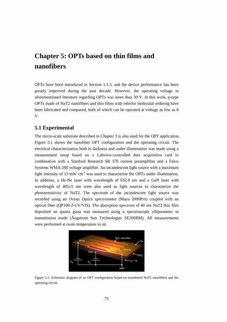
75
Chapter 5: OPTs based on thin films and
nanofibers
OPTs have been introduced in Section 1.1.3, and the device performance has been
greatly improved during the past decade. However, the operating voltage in
aforementioned literature regarding OPTs was more than 30 V. In this work, p-type
OPTs made of NaT2 nanofibers and thin films with inferior molecular ordering have
been fabricated and compared, both of which can be operated at voltage as low as 8
V.
5.1 Experimental
The micro-scale substrate described in Chapter 3 is also used for the OPT application.
Figure 5.1 shows the nanofiber OPT configuration and the operating circuit. The
electrical characterization both in darkness and under illumination was made using a
measurement setup based on a Labview-controlled data acquisition card in
combination with a Stanford Research SR 570 current preamplifier and a Falco
Systems WMA-280 voltage amplifier. An incandescent light source with a maximum
light intensity of 15 mW cm-2
was used to characterize the OPTs under illumination.
In addition, a He-Ne laser with wavelength of 632.8 nm and a GaN laser with
wavelength of 405±5 nm were also used as light sources to characterize the
photosensitivity of NaT2. The spectrum of the incandescent light source was
recorded using an Ocean Optics spectrometer (Maya 2000Pro) coupled with an
optical fiber (QP100-2-UV/VIS). The absorption spectrum of 40 nm NaT2 thin film
deposited on quartz glass was measured using a spectroscopic ellipsometer in
transmission mode (Ångstrom Sun Technologies SE200BM). All measurements
were performed at room temperature in air.
Figure 5.1: Schematic diagram of an OPT configuration based on transferred NaT2 nanofibers and the
operating circuit.
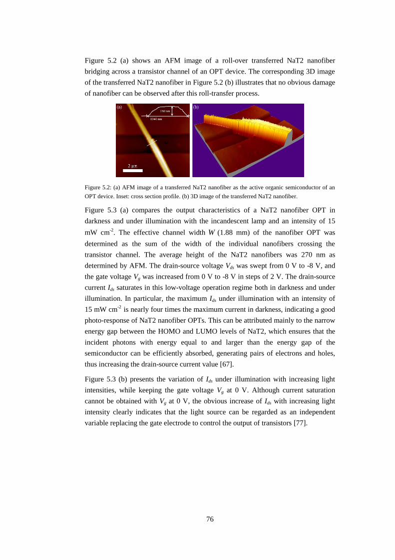
76
Figure 5.2 (a) shows an AFM image of a roll-over transferred NaT2 nanofiber
bridging across a transistor channel of an OPT device. The corresponding 3D image
of the transferred NaT2 nanofiber in Figure 5.2 (b) illustrates that no obvious damage
of nanofiber can be observed after this roll-transfer process.
Figure 5.2: (a) AFM image of a transferred NaT2 nanofiber as the active organic semiconductor of an
OPT device. Inset: cross section profile. (b) 3D image of the transferred NaT2 nanofiber.
Figure 5.3 (a) compares the output characteristics of a NaT2 nanofiber OPT in
darkness and under illumination with the incandescent lamp and an intensity of 15
mW cm-2
. The effective channel width W (1.88 mm) of the nanofiber OPT was
determined as the sum of the width of the individual nanofibers crossing the
transistor channel. The average height of the NaT2 nanofibers was 270 nm as
determined by AFM. The drain-source voltage Vds was swept from 0 V to -8 V, and
the gate voltage Vg was increased from 0 V to -8 V in steps of 2 V. The drain-source
current Ids saturates in this low-voltage operation regime both in darkness and under
illumination. In particular, the maximum Ids under illumination with an intensity of
15 mW cm-2
is nearly four times the maximum current in darkness, indicating a good
photo-response of NaT2 nanofiber OPTs. This can be attributed mainly to the narrow
energy gap between the HOMO and LUMO levels of NaT2, which ensures that the
incident photons with energy equal to and larger than the energy gap of the
semiconductor can be efficiently absorbed, generating pairs of electrons and holes,
thus increasing the drain-source current value [67].
Figure 5.3 (b) presents the variation of Ids under illumination with increasing light
intensities, while keeping the gate voltage Vg at 0 V. Although current saturation
cannot be obtained with Vg at 0 V, the obvious increase of Ids with increasing light
intensity clearly indicates that the light source can be regarded as an independent
variable replacing the gate electrode to control the output of transistors [77].
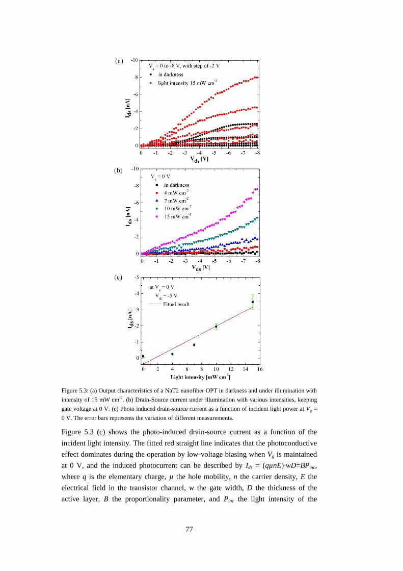
77
Figure 5.3: (a) Output characteristics of a NaT2 nanofiber OPT in darkness and under illumination with
intensity of 15 mW cm-2. (b) Drain-Source current under illumination with various intensities, keeping
gate voltage at 0 V. (c) Photo induced drain-source current as a function of incident light power at Vg =
0 V. The error bars represents the variation of different measurements.
Figure 5.3 (c) shows the photo-induced drain-source current as a function of the
incident light intensity. The fitted red straight line indicates that the photoconductive
effect dominates during the operation by low-voltage biasing when Vg is maintained
at 0 V, and the induced photocurrent can be described by Ids = (qµnE)∙wD=BPinc,
where q is the elementary charge, µ the hole mobility, n the carrier density, E the
electrical field in the transistor channel, w the gate width, D the thickness of the
active layer, B the proportionality parameter, and Pinc the light intensity of the
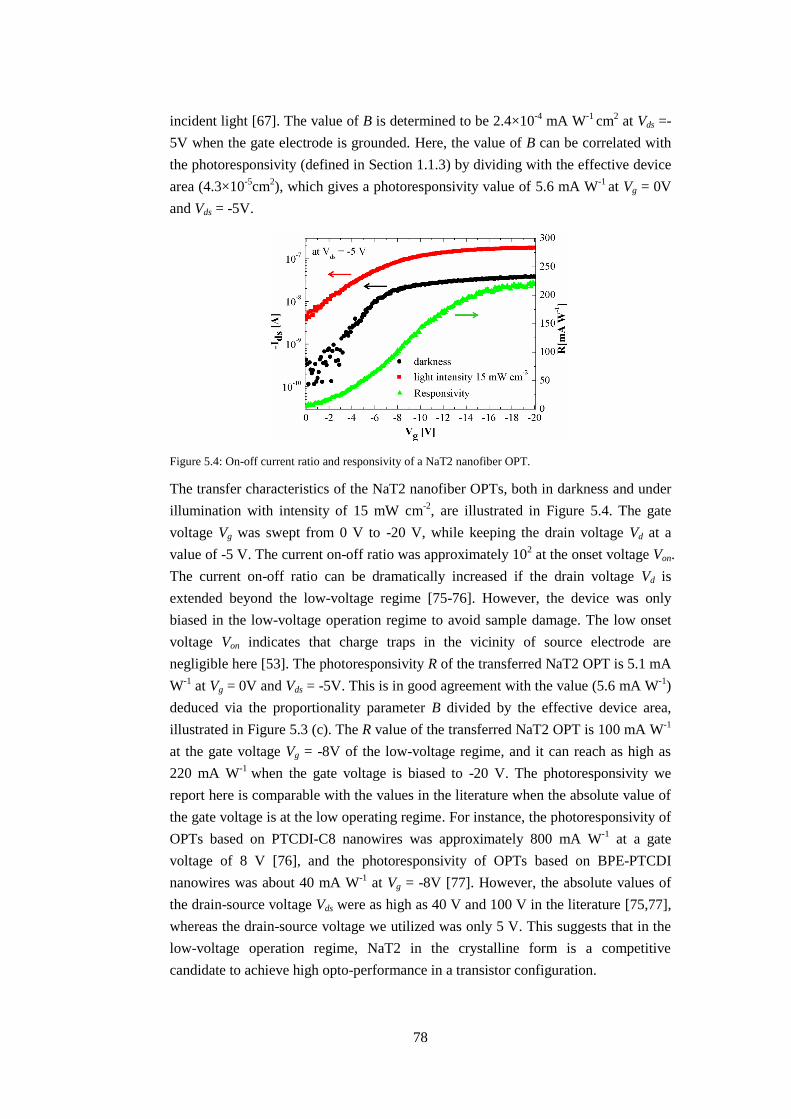
78
incident light [67]. The value of B is determined to be 2.4×10⁻⁴
mA W-1
cm2 at Vds =-
5V when the gate electrode is grounded. Here, the value of B can be correlated with
the photoresponsivity (defined in Section 1.1.3) by dividing with the effective device
area (4.3×10⁻⁵
cm2), which gives a photoresponsivity value of 5.6 mA W
-1 at Vg = 0V
and Vds = -5V.
Figure 5.4: On-off current ratio and responsivity of a NaT2 nanofiber OPT.
The transfer characteristics of the NaT2 nanofiber OPTs, both in darkness and under
illumination with intensity of 15 mW cm-2
, are illustrated in Figure 5.4. The gate
voltage Vg was swept from 0 V to -20 V, while keeping the drain voltage Vd at a
value of -5 V. The current on-off ratio was approximately 102 at the onset voltage Von.
The current on-off ratio can be dramatically increased if the drain voltage Vd is
extended beyond the low-voltage regime [75-76]. However, the device was only
biased in the low-voltage operation regime to avoid sample damage. The low onset
voltage Von indicates that charge traps in the vicinity of source electrode are
negligible here [53]. The photoresponsivity R of the transferred NaT2 OPT is 5.1 mA
W-1
at Vg = 0V and Vds = -5V. This is in good agreement with the value (5.6 mA W-1
)
deduced via the proportionality parameter B divided by the effective device area,
illustrated in Figure 5.3 (c). The R value of the transferred NaT2 OPT is 100 mA W-1
at the gate voltage Vg = -8V of the low-voltage regime, and it can reach as high as
220 mA W-1
when the gate voltage is biased to -20 V. The photoresponsivity we
report here is comparable with the values in the literature when the absolute value of
the gate voltage is at the low operating regime. For instance, the photoresponsivity of
OPTs based on PTCDI-C8 nanowires was approximately 800 mA W-1
at a gate
voltage of 8 V [76], and the photoresponsivity of OPTs based on BPE-PTCDI
nanowires was about 40 mA W-1
at Vg = -8V [77]. However, the absolute values of
the drain-source voltage Vds were as high as 40 V and 100 V in the literature [75,77],
whereas the drain-source voltage we utilized was only 5 V. This suggests that in the
low-voltage operation regime, NaT2 in the crystalline form is a competitive
candidate to achieve high opto-performance in a transistor configuration.
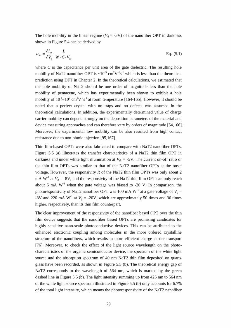
79
The hole mobility in the linear regime (Vd = -5V) of the nanofiber OPT in darkness
shown in Figure 5.4 can be derived by
dslin
g ds
I L
V W C V
Eq. (5.1)
where C is the capacitance per unit area of the gate dielectric. The resulting hole
mobility of NaT2 nanofiber OPT is ~10-5
cm2V
-1s
-1 which is less than the theoretical
prediction using DFT in Chapter 2. In the theoretical calculations, we estimated that
the hole mobility of NaT2 should be one order of magnitude less than the hole
mobility of pentacene, which has experimentally been shown to exhibit a hole
mobility of 10-1
~100 cm
2V
-1s
-1 at room temperature [164-165]. However, it should be
noted that a perfect crystal with no traps and no defects was assumed in the
theoretical calculations. In addition, the experimentally determined value of charge
carrier mobility can depend strongly on the deposition parameters of the material and
device measuring approaches and can therefore vary by orders of magnitude [54,166].
Moreover, the experimental low mobility can be also resulted from high contact
resistance due to non-ohmic injection [95,167].
Thin film-based OPTs were also fabricated to compare with NaT2 nanofiber OPTs.
Figure 5.5 (a) illustrates the transfer characteristics of a NaT2 thin film OPT in
darkness and under white light illumination at Vds = -5V. The current on-off ratio of
the thin film OPTs was similar to that of the NaT2 nanofiber OPTs at the onset
voltage. However, the responsivity R of the NaT2 thin film OPTs was only about 2
mA W-1
at Vg = -8V, and the responsivity of the NaT2 thin film OPT can only reach
about 6 mA W-1
when the gate voltage was biased to -20 V. In comparison, the
photoresponsivity of NaT2 nanofiber OPT was 100 mA W-1
at a gate voltage of Vg =
-8V and 220 mA W-1
at Vg = -20V, which are approximately 50 times and 36 times
higher, respectively, than its thin film counterpart.
The clear improvement of the responsivity of the nanofiber based OPT over the thin
film device suggests that the nanofiber based OPTs are promising candidates for
highly sensitive nano-scale photoconductive devices. This can be attributed to the
enhanced electronic coupling among molecules in the more ordered crystalline
structure of the nanofibers, which results in more efficient charge carrier transport
[76]. Moreover, to check the effect of the light source wavelength on the photo-
characteristics of the organic semiconductor device, the spectrum of the white light
source and the absorption spectrum of 40 nm NaT2 thin film deposited on quartz
glass have been recorded, as shown in Figure 5.5 (b). The theoretical energy gap of
NaT2 corresponds to the wavelength of 564 nm, which is marked by the green
dashed line in Figure 5.5 (b). The light intensity summing up from 425 nm to 564 nm
of the white light source spectrum illustrated in Figure 5.5 (b) only accounts for 6.7%
of the total light intensity, which means the photoresponsivity of the NaT2 nanofiber
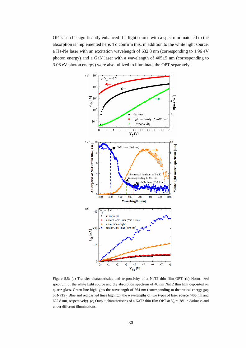
80
OPTs can be significantly enhanced if a light source with a spectrum matched to the
absorption is implemented here. To confirm this, in addition to the white light source,
a He-Ne laser with an excitation wavelength of 632.8 nm (corresponding to 1.96 eV
photon energy) and a GaN laser with a wavelength of 405±5 nm (corresponding to
3.06 eV photon energy) were also utilized to illuminate the OPT separately.
Figure 5.5: (a) Transfer characteristics and responsivity of a NaT2 thin film OPT. (b) Normalized
spectrum of the white light source and the absorption spectrum of 40 nm NaT2 thin film deposited on
quartz glass. Green line highlights the wavelength of 564 nm (corresponding to theoretical energy gap
of NaT2). Blue and red dashed lines highlight the wavelengths of two types of laser source (405 nm and
632.8 nm, respectively). (c) Output characteristics of a NaT2 thin film OPT at Vg = -8V in darkness and
under different illuminations.
81
As shown in the output characteristics in Figure 5.5 (c), under the illumination of the
white light source, the drain-source current is more than doubled compared with that
in darkness at Vds = -8V. However, even though the intensity of the HeNe laser was
tuned to be 24 mW cm-2
, which is 60% higher than the maximum light intensity of
the white light source (15 mW cm-2
), no obvious difference of the drain-source
current at Vds = -8V can be observed between the output characteristics of the
illuminated and non-illuminated NaT2 thin film-based OPT. This can be explained
by the fact that a photon energy of 1.96 eV is not sufficient to generate additional
photo carriers to contribute to the drain-source current in the transistor channel.
When we utilized the GaN laser with a wavelength of 405±5 nm as another
independent light source, however, we could observe an approximately four-fold
increase of the drain-source current compared to the current measured in darkness,
even though the light intensity of the 405 nm diode laser was tuned to be 8 mW cm-2
,
which is only half the maximum light intensity of the white light source. Thus, a
good matching of the light source spectrum with the absorption spectrum of the
organic semiconductor in OPTs is of great importance to maximize the device
performance. In particular, a light source spectrum with wavelengths predominantly
below 564 nm should be considered to fully match with the absorption spectrum of
NaT2.
The ratio of GaN laser-induced drain-source current and the current induced by white
light, which can be found from the data in Figure 5.5 (c) as
( ) / ( ) 3.3 0.4GaN dark WL darkI I I I , can indicate that the HOMO/LUMO energy
gap of NaT2 is underestimated by DFT calculation shown in Figure 2.4. This is
because the input number of photons per second and the illumination induced
number of holes per second can be correlated as
GaN GaN darkGaN
GaN
P I I
e q
Eq. (5.2)
WL WL darkWL
WL
P I I
e q
Eq. (5.3)
where P is the input power of the GaN laser or the white light, e is the photon energy,
α is the absorption coefficient, I is drain-source current under different illuminating
conditions, and q is the elementary charge. From Eq. (5.2) and (5.3), the following
equation can be obtained
/
/
GaN GaN GaN GaN dark
WL WL WL WL dark
P e I I
P e I I
. Eq. (5.4)
Since the light intensity integrated from 425 nm to 564 nm of the white light source
spectrum in Figure 5.5 (b) only accounts for 6.7% of the total light intensity, the
82
input power ratio /GaN WLP P is equal to the light intensity ratio /GaN WL
inc incP P , which
is8 / (15 0.067) 7.96 . The ratio of ( / ) / ( / )GaN GaN WL WLe e can be determined by
integration of the absorption spectrum corresponding to the GaN laser (from 400 nm
to 410 nm) and the white light source (from 425 nm to 564 nm), respectively, and
this ratio is found to be 0.14. Therefore, using the DFT calculated energy gap
(corresponding to 564 nm) of NaT2, the left-hand side of Eq. (5.4) can be determined
to be 7.96 0.14 1.1 , which is only 33% of the current ratio. However, as
mentioned previously, the theoretical value of the NaT2 energy gap could be
underestimated by roughly 10%. Thus, we took the wavelength of 512 nm,
corresponding to 2.2×(1+0.1) eV, as another reference point and repeat the above
integration process. Following this approach the left-hand side of Eq. (5.4) is
determined to be 22.42 0.17 3.8 , which is only 15% larger than the value of the
current ratio ( ) / ( )GaN dark WL darkI I I I . Therefore, this suggests that the DFT
calculations underestimate the energy gap of NaT2. Moreover, it reveals that the light
source wavelength plays an important role in determining the phototransistor
performance.
5.2 Chapter summary
OPTs based on transferred NaT2 nanofibers with highly crystallinity and NaT2 thin
films with lower molecular ordering have been fabricated and characterized in
darkness and under illumination. The obvious superior responsivity of the nanofiber-
based OPTs compared with thin film OPTs clearly demonstrates that the transferred
NaT2 nanofiber have great potential for high-performance photosensitive devices,
mainly attributed to the highly ordered molecular packing in the crystalline structures.
83
Chapter 6: Conclusions and outlook
Organic light-emitting transistors (OLETs) have the potential to replace organic
light-emitting diodes (OLEDs) as the critical components of the next generation
light-emitting devices. In the planar configuration of a bottom contact transistor
platform, the electroluminescence from recombination of charge carriers can be
directly extracted without being blocked by a top metal electrode. The transistor
configuration also provides an excellent platform to investigate the charge injection
from metal electrode to organic semiconductor.
Organic materials based on small molecules both in the form of thin films and
nanofibers have been used in this work as the active organic semiconductor in the
transistor platform. The organic thin films can be directly deposited on transistor
substrates under high vacuum conditions to form amorphous-like semiconductors.
The nanofibers are mainly deposited on particular surface, namely the surface of
muscovite mica, to form one dimensional nano-aggregates, and then transferred onto
transistor substrates via a directly vertical stamping or a roll-on transfer technique.
The photoluminescence from the organic thin films and nanofibers have been
characterized mainly using fluorescence microscopy and spectrometer. The main
peaks of the photoluminescence spectra are in agreement with the energy difference
between HOMO/LUMO levels and their corresponding vibrational energy levels.
The emission spectra of transferred p6P nanofibers have also been studied in a
temperature dependent manner to show that the nanofibers resemble the good fiber
arrays after transfer.
Theoretical investigations have been carried out regarding various small-molecule
based organic materials. Density functional theory (DFT) calculations have been
performed to estimate and compare the charge carrier transport property and the
optical property of the organic materials.
Conventional OLETs are driven by a DC gate voltage together with DC voltage
applied to metal electrodes. Electrons and holes are injected from opposite metal
electrodes to recombine in the transistor channel to give rise to electroluminescence.
Unlike the DC biasing method, the OLETs driven by AC gate voltage have been
investigated. In the AC-driven OLETs, charge carriers of opposite polarities can be
injected from an individual metal electrode in the different operating regimes of the
AC voltage. The injection of one type of charge carriers is facilitated by the space-
charge field formed by previously injected charge carriers of the other polarity.
84
Organic thin films are mainly applied as the active organic semiconductors in the
transistor platform to investigate the operating mechanism of the AC-driven OLETs.
This operating mechanism is also valid in the organic nanofiber-based OLETs.
Organic phototransistors (OPTs) as the light detectors can be integrated into novel
optoelectronic devices, particularly in an OLET-included lab-on-a-chip system.
OPTs based on organic nanofibers and thin films have been fabricated and
characterized in darkness and under illumination. The obvious superior
photoresponsivity of the nanofiber-based OPTs compared with thin film OPTs
demonstrates that nanofibers have great potential for high-performance
photosensitive devices, mainly attributed to the highly ordered molecular packing in
the crystalline structures.
Future work could involve more integration of self-assembled monolayers (SAMs),
both in modifying the metal electrode and the semiconductor/dielectric interface, so
as to optimize the charge carrier injection and transport. The spatial variation of the
emission zone in AC-driven OLETs could be also optimized by the SAMs
modification.
The gate dielectric in transistor used in this work is mainly silicon dioxide which
prohibits the integration of flexible substrates. In the future, apart from the possibility
of utilizing polymer dielectric, ultra thin layers of muscovite mica could be
implemented as the gate dielectric of organic nanofiber-based transistors. For
fabricating this type of transistors, it is not necessary to firstly deposit organic
nanofibers on mica and subsequently transfer the fibers onto transistor platform.
Instead, the organic nanofibers can be in-situ grown onto the transistor substrates
with thin layers of mica as the dielectric.
As for the application of OPTs, a top contact transistor configuration can be
implemented in future work to enhance the charge carrier mobility under low-voltage
operation. Besides, a better matching of the light source spectrum with the absorption
spectrum of the organic semiconductor should be realized to optimize the device
performance.
85
Appendices
A: List of publications
Conduction and electroluminescence from organic continuous and nanofiber
thin films, Jakob Kjelstrup-Hansen, Xuhai Liu, Henrik H. Henrichsen,
Kasper Thilsing-Hansen, and Horst-Günter Rubahn, Physica Status Solidi C,
Vol. 7, Nr. 11-12, 2763-2766 (2010).
AC-biased organic light-emitting field-effect transistors from naphthyl end-
capped oligothiophenes, Xuhai Liu, Ivonne Wallmann, Henri Boudinov,
Jakob Kjelstrup-Hansen, Manuela Schiek, Arne Lützen, and Horst-Günter
Rubahn, Organic Electronics, Vol. 11, 1096-1102 (2010).
Charge-carrier injection assisted by space-charge field in AC-driven organic
light-emitting transistors, Xuhai Liu, Jakob Kjelstrup-Hansen, Henri
Boudinov, and Horst-Günter Rubahn, Organic Electronics, Vol. 12, 1724-
1730 (2011).
Optical properties of microstructured surface-grown and transferred organic
nanofibers, Jakob Kjelstrup-Hansen, Luciana Tavares, Roana Melina de
Oliveira Hansen, Xuhai Liu, Kirill Bordo, and Horst-Günter Rubahn,
Journal of Nanophotonics, Vol. 5, Nr. 051701 (2011).
A strain sensor based on an aligned carbon particle string in a UV-cured
polymer matrix, Henrik Høyer, Matti Knaapila, Jakob Kjelstrup-Hansen,
Xuhai Liu, and Geir Helgesen, Applied Physics Letters, Vol. 99, Nr. 213106
(2011).
AC-driven light emission from in-situ grown organic nanofibers, Xuhai Liu,
Jakob Kjelstrup-Hansen, Roana Melina de Oliveira Hansen, Morten Madsen,
and Horst-Günter Rubahn, Proceedings of SPIE, the International Society
for Optical Engineering, Vol. 8435, Nr. 843524 (2012).
Organic light-emitting transistors optimized by self-assembled monolayers,
Fei Liu, Jakob Kjelstrup-Hansen, Xuhai Liu, and Horst-Günter Rubahn,
Proceedings of SPIE, the International Society for Optical Engineering, Vol.
8435, s. 84351C/1-7 (2012).
Individual strings of conducting carbon cones and discs in a polymer matrix:
Electric field-induced alignment and their use as a strain sensor, Henrik
Høyer, Matti Knaapila, Jakob Kjelstrup-Hansen, Xuhai Liu, and Geir
Helgesen, Journal of Polymer Science, Part B, Polymer Physics, Vol. 50,
Nr. 7, 477-483 (2012).
86
A.1: Conference participation
TNT 2009 Trends in NanoTechnology
Barcelona, Spain Sep. 07-11, 2009
Presented a poster on “Conduction and electroluminescence from organic
continuous and nanofiber thin films”.
12th Conference “Advanced Materials and Technologies” and summer
school “European Doctorate in Physics and Chemistry of Advanced
Materials”
Palanga, Lithuania Aug. 27-31, 2010
Presented a poster on “Space-charge assisted electron tunneling in AC-
driven organic light emitting transistors”.
E-MRS Spring Meeting 2011
Nice, France May. 9-13, 2011
Oral presentation on “Light emission from organic thin film transistors”.
SPIE 2012 Photonics Europe
Brussels, Belgium Apr. 16-19, 2012
Presented a poster on “AC-driven light emission from in-situ grown organic
nanofibers”.
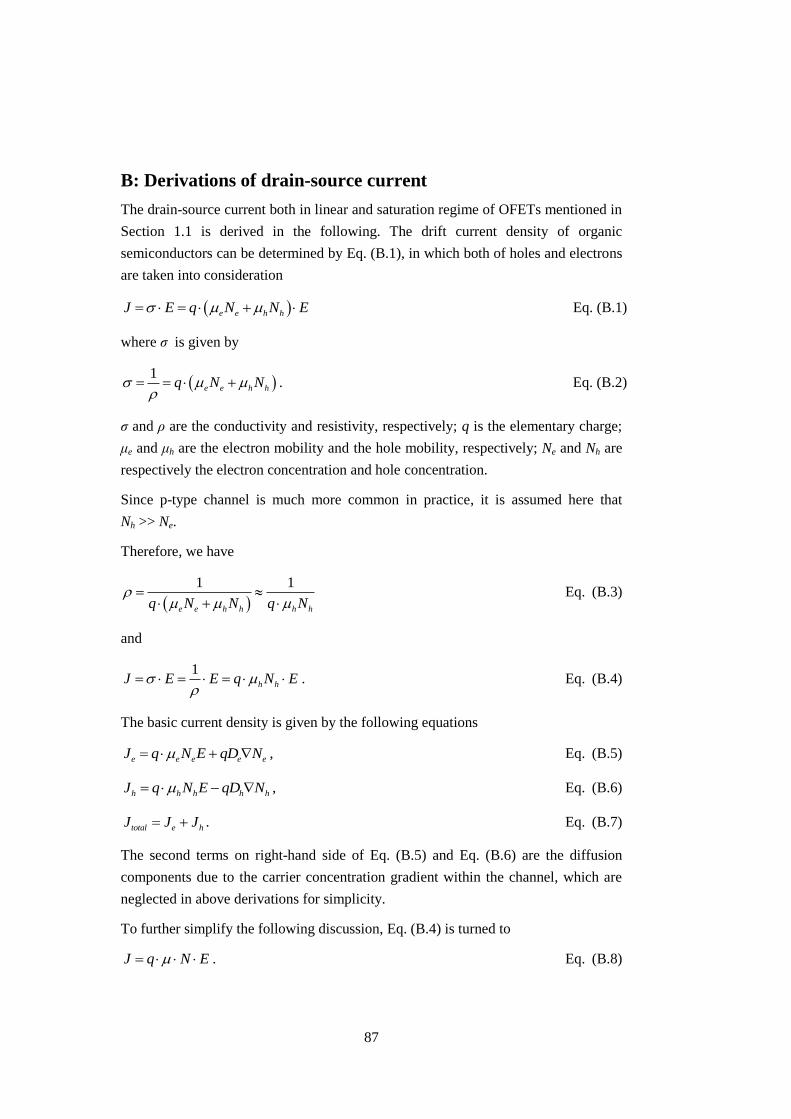
87
B: Derivations of drain-source current
The drain-source current both in linear and saturation regime of OFETs mentioned in
Section 1.1 is derived in the following. The drift current density of organic
semiconductors can be determined by Eq. (B.1), in which both of holes and electrons
are taken into consideration
e e h hJ E q N N E Eq. (B.1)
where σ is given by
1
e e h hq N N
. Eq. (B.2)
σ and ρ are the conductivity and resistivity, respectively; q is the elementary charge;
μe and μh are the electron mobility and the hole mobility, respectively; Ne and Nh are
respectively the electron concentration and hole concentration.
Since p-type channel is much more common in practice, it is assumed here that
Nh >> Ne.
Therefore, we have
1 1
e e h h h hq N N q N
Eq. (B.3)
and
1h hJ E E q N E
. Eq. (B.4)
The basic current density is given by the following equations
e e e e eJ q N E qD N , Eq. (B.5)
h h h h hJ q N E qD N , Eq. (B.6)
total e hJ J J . Eq. (B.7)
The second terms on right-hand side of Eq. (B.5) and Eq. (B.6) are the diffusion
components due to the carrier concentration gradient within the channel, which are
neglected in above derivations for simplicity.
To further simplify the following discussion, Eq. (B.4) is turned to
J q N E . Eq. (B.8)
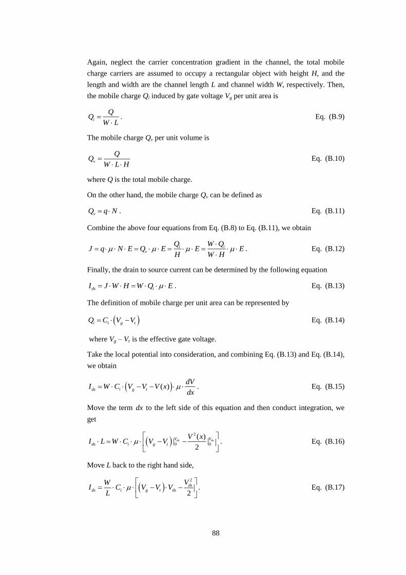
88
Again, neglect the carrier concentration gradient in the channel, the total mobile
charge carriers are assumed to occupy a rectangular object with height H, and the
length and width are the channel length L and channel width W, respectively. Then,
the mobile charge Qi induced by gate voltage Vg per unit area is
i
W L
. Eq. (B.9)
The mobile charge Qv per unit volume is
v
W L H
Eq. (B.10)
where Q is the total mobile charge.
On the other hand, the mobile charge Qv can be defined as
vQ q N . Eq. (B.11)
Combine the above four equations from Eq. (B.8) to Eq. (B.11), we obtain
i iv
Q W QJ q N E Q E E E
H W H
. Eq. (B.12)
Finally, the drain to source current can be determined by the following equation
ds iI J W H W Q E . Eq. (B.13)
The definition of mobile charge per unit area can be represented by
i i g tQ C V V Eq. (B.14)
where Vg – Vt is the effective gate voltage.
Take the local potential into consideration, and combining Eq. (B.13) and Eq. (B.14),
we obtain
( )ds i g t
dVI W C V V V x
dx . Eq. (B.15)
Move the term dx to the left side of this equation and then conduct integration, we
get
2
0 0
( )| |
2ds dsV V
ds i g t
V xI L W C V V
. Eq. (B.16)
Move L back to the right hand side,
2
2
dsds i g t ds
VWI C V V V
L
. Eq. (B.17)
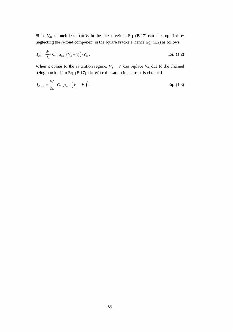
89
Since Vds is much less than Vg in the linear regime, Eq. (B.17) can be simplified by
neglecting the second component in the square brackets, hence Eq. (1.2) as follows.
ds i lin g t ds
WI C V V V
L . Eq. (1.2)
When it comes to the saturation regime, Vg – Vt can replace Vds due to the channel
being pinch-off in Eq. (B.17), therefore the saturation current is obtained
2
,2
ds sat i sat g t
WI C V V
L . Eq. (1.3)

90
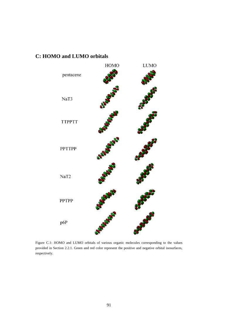
91
C: HOMO and LUMO orbitals
Figure C.1: HOMO and LUMO orbitals of various organic molecules corresponding to the values
provided in Section 2.2.1. Green and red color represent the positive and negative orbital isosurfaces,
respectively.

92
93
D: Micro-scale device fabrication recipe
The micro-scale transistor substrate which is started with a 4-inch Si/SiO2 wafer, is
patterned by optical lithography and fabricated through standard cleanroom process.
The recipe of making Au electrode is described in the following.
Hexamethyldisilane (HMDS) treatment for 30 min. in HMDS oven. The
HMDS monolayer is the adhesion promoter between SiO2 of the wafer and
subsequently deposited photoresist.
Spincoat of an image reversal photoresist AZ 5214 (paras: 500 rpm for 5 sec.;
4000 rpm for 30 sec.).
Pre-bake the wafer on hotplate at 100 °C for 60 sec.
UV exposure of the photoresist for 2.5 sec on mask aligner. Note that the
exposure time could be altered after equipment maintenance, and new
optimized exposure time should be tested in this case.
Post-bake the wafer on hotplate at 120 °C for 100 sec, to make the exposed
soluble photoresist insoluble in developer.
Flood exposure of the photoresist for 30 sec, to make the previously
unexposed photoresist soluble in developer.
Development in AZ 351B at 22 °C for 1 min., which is followed by 2 min.
water rinse.
Spin-dry the wafer and deposit Ti/Au using an e-beam evaporator (Cryofox
600) at a rate of 2 Å/sec.
Lift-off in acetone wet bench, then repeat the rinse and spin-dry process.
The process to fabricate the back gate electrode (see Figure 3.2) is generally the same
as the above procedure, except that the SiO2 corresponding to the gate contact pad
has to be etched using buffered HF before depositing Ti/Au

94
95
E: Extraction of emission intensity of p6P thin film based
OLET
The extraction of emission intensity of p6P-based OLET in Section 3.2.3 is presented
in the following.
Firstly, a photomultiplier tube (PMT) (Hamamatsu R943-02) as the light detector
was calibrated. A He-Ne laser with wavelength of 632.8 nm (input power: 3000 µW)
was used as the known light source. A group of filters (three Neutral Density filters
and one VBA-200 beam splitter) were used to reduce the laser light input into the
PMT. The input number of photons per second and the output number of electrons
per second can be correlated as
int
0
P IG
e q Eq. (E.1)
where Pint is the input power, e0 is the energy of one photon (632.8 nm), q is the
elementary charge, I is the output current (monitored by a 610C Solid State
Electrometer), η is the quantum efficiency of the PMT. The calibrated gain of the
PMT is thus written as
0
int
1eIG
P q Eq. (E.2)
where e0 = 1.96×1.6×10-19
J, I = 1.1×10⁻⁶
A (directly read from the electrometer when
the PMT was powered by a voltage of 900 V), η = 14% at the wavelength of 632.8
nm, q = 1.6×10⁻¹⁹
A·s. Pint is the laser power after passing through the filters. Based
on the above parameters, the calibrated PMT gain is G = 2600±600.
Next, the collecting efficiency of the incident light was estimated. The p6P-based
device is assumed as a Lambert emitter, and the luminous intensity of the p6P emitter
is defined by the well-known Lambert’s cosine law, with peak luminous intensity in
the normal direction. The collecting efficiency σ is defined as
eff
total
F
F Eq. (E.3)
where Ftotal is the total luminous flux, which is
/2
max
0
sin(2 )2
2totalF I d
Eq. (E.4)
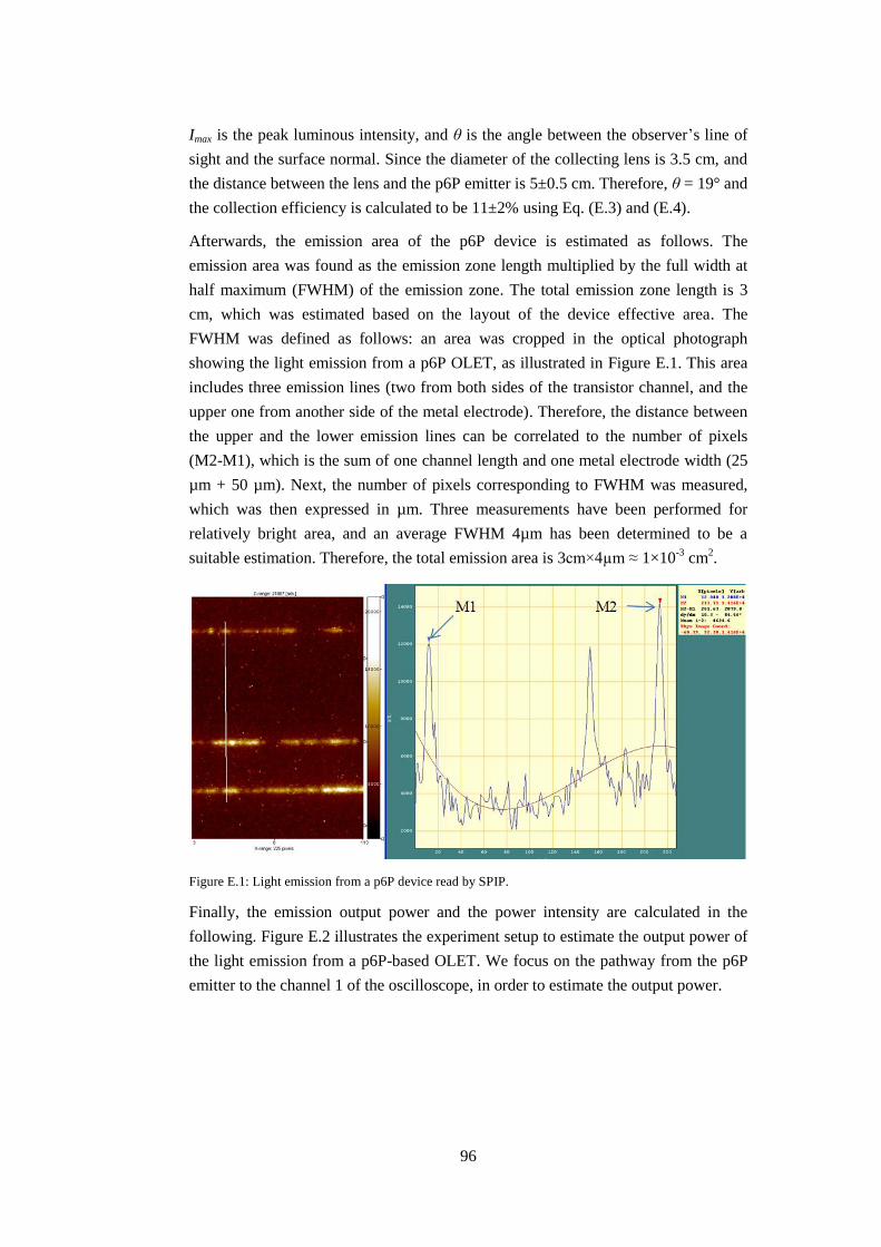
96
Imax is the peak luminous intensity, and θ is the angle between the observer’s line of
sight and the surface normal. Since the diameter of the collecting lens is 3.5 cm, and
the distance between the lens and the p6P emitter is 5±0.5 cm. Therefore, θ = 19° and
the collection efficiency is calculated to be 11±2% using Eq. (E.3) and (E.4).
Afterwards, the emission area of the p6P device is estimated as follows. The
emission area was found as the emission zone length multiplied by the full width at
half maximum (FWHM) of the emission zone. The total emission zone length is 3
cm, which was estimated based on the layout of the device effective area. The
FWHM was defined as follows: an area was cropped in the optical photograph
showing the light emission from a p6P OLET, as illustrated in Figure E.1. This area
includes three emission lines (two from both sides of the transistor channel, and the
upper one from another side of the metal electrode). Therefore, the distance between
the upper and the lower emission lines can be correlated to the number of pixels
(M2-M1), which is the sum of one channel length and one metal electrode width (25
µm + 50 µm). Next, the number of pixels corresponding to FWHM was measured,
which was then expressed in µm. Three measurements have been performed for
relatively bright area, and an average FWHM 4µm has been determined to be a
suitable estimation. Therefore, the total emission area is 3cm×4µm ≈ 1×10⁻³
cm2.
Figure E.1: Light emission from a p6P device read by SPIP.
Finally, the emission output power and the power intensity are calculated in the
following. Figure E.2 illustrates the experiment setup to estimate the output power of
the light emission from a p6P-based OLET. We focus on the pathway from the p6P
emitter to the channel 1 of the oscilloscope, in order to estimate the output power.
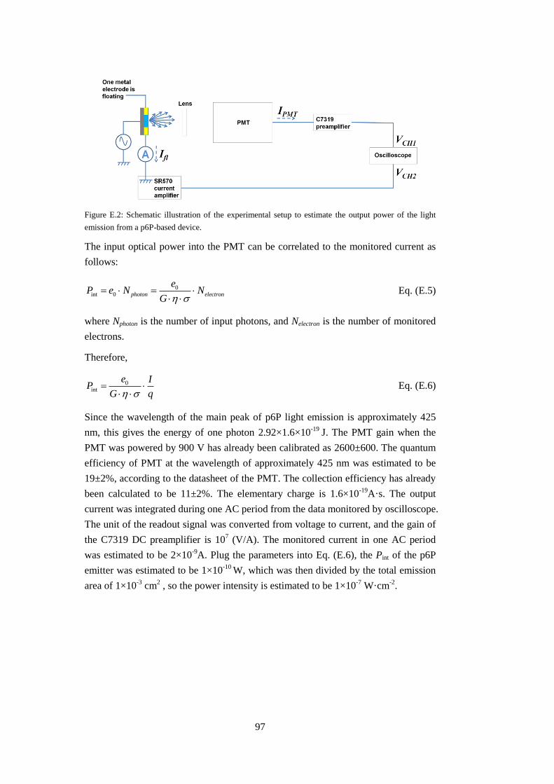
97
Figure E.2: Schematic illustration of the experimental setup to estimate the output power of the light
emission from a p6P-based device.
The input optical power into the PMT can be correlated to the monitored current as
follows:
0int 0 photon electron
eP e N N
G
Eq. (E.5)
where Nphoton is the number of input photons, and Nelectron is the number of monitored
electrons.
Therefore,
0int
e IP
G q
Eq. (E.6)
Since the wavelength of the main peak of p6P light emission is approximately 425
nm, this gives the energy of one photon 2.92×1.6×10-19
J. The PMT gain when the
PMT was powered by 900 V has already been calibrated as 2600±600. The quantum
efficiency of PMT at the wavelength of approximately 425 nm was estimated to be
19±2%, according to the datasheet of the PMT. The collection efficiency has already
been calculated to be 11±2%. The elementary charge is 1.6×10⁻¹⁹
A·s. The output
current was integrated during one AC period from the data monitored by oscilloscope.
The unit of the readout signal was converted from voltage to current, and the gain of
the C7319 DC preamplifier is 107 (V/A). The monitored current in one AC period
was estimated to be 2×10⁻⁹
A. Plug the parameters into Eq. (E.6), the Pint of the p6P
emitter was estimated to be 1×10⁻¹⁰
W, which was then divided by the total emission
area of 1×10⁻³
cm2 , so the power intensity is estimated to be 1×10
-7 W·cm
-2.

98
99
Bibliography
1 Huang, M. H., Mao, S., Feick, H., Yan, H. Q., Wu, Y. Y., Kind, H., Weber, E.,
Russo, R. & Yang, P. D. Room-temperature ultraviolet nanowire nanolasers.
Science 292, 1897-1899, (2001).
2 Huang, Y., Duan, X. F. & Lieber, C. M. Nanowires for integrated multicolor
nanophotonics. Small 1, 142-147, (2005).
3 Pettersson, H., Tragardh, J., Persson, A. I., Landin, L., Hessman, D. &
Samuelson, L. Infrared photodetectors in heterostructure nanowires. Nano
Letters 6, 229-232, (2006).
4 Wang, Z. L. Progress in Piezotronics and Piezo-Phototronics. Advanced
Materials 24, 4632-4646, (2012).
5 Sze, S. E. Semiconductor devices: Physics and technology, 2nd ed. John
Wiley&Sons, New York, (2002).
6 Lee, H., Yoo, G., Yoo, J. S. & Kanicki, J. Asymmetric electrical properties of
fork a-Si:H thin-film transistor and its application to flat panel displays. Journal
of Applied Physics 105, (2009).
7 Kuo, A., Won, T. K. & Kanicki, J. Advanced amorphous silicon thin-film
transistors for AM-OLEDs: Electrical performance and stability. Ieee
Transactions on Electron Devices 55, 1621-1629, (2008).
8 Cherenack, K. H., Hekmatshoar, B., Sturm, J. C. & Wagner, S. Self-Aligned
Amorphous Silicon Thin-Film Transistors Fabricated on Clear Plastic at 300
degrees C. Ieee Transactions on Electron Devices 57, 2381-2389, (2010).
9 Zhang, D., Choy, W. C. H., Xie, F. X. & Li, X. C. Large-area, high-quality self-
assembly electron transport layer for organic optoelectronic devices. Organic
Electronics 13, 2042-2046, (2012).
10 Wright, M. & Uddin, A. Organic-inorganic hybrid solar cells: A comparative
review. Sol. Energy Mater. Sol. Cells 107, 87-111, (2012).
11 Sirringhaus, H., Tessler, N. & Friend, R. H. Integrated optoelectronic devices
based on conjugated polymers. Science 280, 1741-1744, (1998).
12 Sessolo, M. & Bolink, H. J. Hybrid Organic-Inorganic Light-Emitting Diodes.
Advanced Materials 23, 1829-1845, (2011).
100
13 Lipomi, D. J., Lee, J. A., Vosgueritchian, M., Tee, B. C. K., Bolander, J. A. &
Bao, Z. A. Electronic Properties of Transparent Conductive Films of
PEDOT:PSS on Stretchable Substrates. Chem. Mat. 24, 373-382, (2012).
14 Henson, Z. B., Mullen, K. & Bazan, G. C. Design strategies for organic
semiconductors beyond the molecular formula. Nat. Chem. 4, 699-704, (2012).
15 Irimia-Vladu, M., Marjanovic, N., Vlad, A., Ramil, A. M., Hernandez-Sosa, G.,
Schwodiauer, R., Bauer, S. & Sariciftci, N. S. Vacuum-Processed Polyaniline-
C-60 Organic Field Effect Transistors. Advanced Materials 20, 3887-+, (2008).
16 Zhao, Q., Kim, T. H., Park, J. W., Kim, S. O., Jung, S. O., Kim, J. W., Ahn, T.,
Kim, Y. H., Yi, M. H. & Kwon, S. K. High-Performance Semiconductors based
on Alkoxylnaphthyl End-Capped Oligomers for Organic Thin-Film Transistors.
Advanced Materials 20, 4868-+, (2008).
17 Sandberg, H. G. O., Backlund, T. G., Osterbacka, R. & Stubb, H. High-
performance all-polymer transistor utilizing a hygroscopic insulator. Advanced
Materials 16, 1112-+, (2004).
18 Wang, S. H., Kappl, M., Liebewirth, I., Muller, M., Kirchhoff, K., Pisula, W. &
Mullen, K. Organic Field-Effect Transistors based on Highly Ordered Single
Polymer Fibers. Advanced Materials 24, 417-+, (2012).
19 Cooper, K. P. & Tms. MATERIALS AND MANUFACTURING CHALLENGES
IN HYBRID FLEXIBLE ELECTRONICS. (Minerals, Metals & Materials Soc,
2010).
20 Fujisaki, Y., Nakajima, Y., Takei, T., Fukagawa, H., Yamamoto, T. & Fujikake,
H. Flexible Active-Matrix Organic Light-Emitting Diode Display Using Air-
Stable Organic Semiconductor of Dinaphtho 2, 3-b: 2 ', 3 '-f thieno 3, 2-b -
thiophene. Ieee Transactions on Electron Devices 59, 3442-3449, (2012).
21 Ramuz, M., Tee, B. C. K., Tok, J. B. H. & Bao, Z. N. Transparent, Optical,
Pressure-Sensitive Artificial Skin for Large-Area Stretchable Electronics.
Advanced Materials 24, 3223-3227, (2012).
22 Lipomi, D. J., Vosgueritchian, M., Tee, B. C. K., Hellstrom, S. L., Lee, J. A.,
Fox, C. H. & Bao, Z. N. Skin-like pressure and strain sensors based on
transparent elastic films of carbon nanotubes. Nature Nanotechnology 6, 788-
792, (2011).
23 Shang, S. M., Zeng, W. & Tao, X. M. High stretchable MWNTs/polyurethane
conductive nanocomposites. Journal of Materials Chemistry 21, 7274-7280,
(2011).
101
24 Pais, A., Banerjee, A., Klotzkin, D. & Papautsky, I. High-sensitivity, disposable
lab-on-a-chip with thin-film organic electronics for fluorescence detection. Lab
Chip 8, 794-800, (2008).
25 Sun, Q. J., Dong, G. F., Wang, L. D. & Qiu, Y. Organic optocouplers. Sci.
China-Chem. 54, 1017-1026, (2011).
26 Anthopoulos, T. D., Tanase, C., Setayesh, S., Meijer, E. J., Hummelen, J. C.,
Blom, P. W. M. & de Leeuw, D. M. Ambipolar organic field-effect transistors
based on a solution-processed methanofullerene. Advanced Materials 16, 2174-
+, (2004).
27 Baeg, K. J., Noh, Y. Y., Ghim, J., Kang, S. J., Lee, H. & Kim, D. Y. Organic
non-volatile memory based on pentacene field-effect transistors using a
polymeric gate electret. Advanced Materials 18, 3179-+, (2006).
28 Madec, M. B., Morrison, J. J., Sanchez-Romaguera, V., Turner, M. L. & Yeates,
S. G. Organic field effect transistors from ambient solution processed
poly(triarylamine)-insulator blends. Journal of Materials Chemistry 19, 6750-
6755, (2009).
29 Balzer, F. & Rubahn, H. G. Growth control and optics of organic
nanoaggregates. Advanced Functional Materials 15, 17-24, (2005).
30 Kjelstrup-Hansen, J., Boggild, P. & Rubahn, H. G. Charge Injection and
Transport in Organic Nanofibers. Proceedings of the International Conference
on Nanoscience and Technology 61, 565-569, (2007).
31 Schiek, M., Lutzen, A., Koch, R., Al-Shamery, K., Balzer, F., Frese, R. &
Rubahn, H. G. Nanofibers from functionalized para-phenylene molecules.
Applied Physics Letters 86, (2005).
32 Bernanose, A. ELECTROLUMINESCENCE OF ORGANIC COMPOUNDS.
British Journal of Applied Physics, S54-S56, (1955).
33 Bernanose, A., Comte, M. & Vouaux, P. *SUR UN NOUVEAU MODE
DEMISSION LUMINEUSE CHEZ CERTAINS COMPOSES ORGANIQUES.
J. Chim. Phys.-Chim. Biol. 50, 64-68, (1953).
34 Bernanose, A. & Vouaux, P. *ELECTROLUMINESCENCE ORGANIQUE -
ETUDE DU MODE DEMISSION. J. Chim. Phys.-Chim. Biol. 50, 261-&,
(1953).
35 Pope, M., Magnante, P. & Kallmann, H. P. ELECTROLUMINESCENCE IN
ORGANIC CRYSTALS. J. Chem. Phys. 38, 2042-&, (1963).
102
36 Tang, C. W. & Vanslyke, S. A. ORGANIC ELECTROLUMINESCENT
DIODES. Applied Physics Letters 51, 913-915, (1987).
37 Burroughes, J. H., Bradley, D. D. C., Brown, A. R., Marks, R. N., Mackay, K.,
Friend, R. H., Burns, P. L. & Holmes, A. B. LIGHT-EMITTING-DIODES
BASED ON CONJUGATED POLYMERS. Nature 347, 539-541, (1990).
38 Braun, D. & Heeger, A. J. VISIBLE-LIGHT EMISSION FROM
SEMICONDUCTING POLYMER DIODES. Applied Physics Letters 58, 1982-
1984, (1991).
39 Braun, D., Moses, D., Zhang, C. & Heeger, A. J. NANOSECOND
TRANSIENT ELECTROLUMINESCENCE FROM POLYMER LIGHT-
EMITTING-DIODES. Applied Physics Letters 61, 3092-3094, (1992).
40 Sariciftci, N. S., Braun, D., Zhang, C., Srdanov, V. I., Heeger, A. J., Stucky, G.
& Wudl, F. SEMICONDUCTING POLYMER-BUCKMINSTERFULLERENE
HETEROJUNCTIONS - DIODES, PHOTODIODES, AND PHOTOVOLTAIC
CELLS. Applied Physics Letters 62, 585-587, (1993).
41 Budzelaar, F. P. M., Cordes, C. N., Hoppenbrouwers, J. J. L., van der Vaart, N.
C., van Beek, W. H. M., Vossen, F. J., Hoevenaars, A. A. M. & Boom, R. G. H.
Video processing for active-matrix polymer OLED TV. J. Soc. Inf. Disp. 14,
461-466, (2006).
42 Chen, S. Z., Peng, S. H., Ting, T. Y., Wu, P. S., Lin, C. H., Chang, C. Y., Shyue,
J. J. & Jou, J. H. Organic light-emitting diodes with direct contact-printed red,
green, blue, and white light-emitting layers. Applied Physics Letters 101, (2012).
43 Fyfe, D. Organic displays come of age. Nat. Photonics 3, 453-455, (2009).
44 Adachi, C., Baldo, M. A., Thompson, M. E. & Forrest, S. R. Nearly 100%
internal phosphorescence efficiency in an organic light-emitting device. Journal
of Applied Physics 90, 5048-5051, (2001).
45 Cao, Y., Parker, I. D., Yu, G., Zhang, C. & Heeger, A. J. Improved quantum
efficiency for electroluminescence in semiconducting polymers. Nature 397,
414-417, (1999).
46 Baldo, M. A., Lamansky, S., Burrows, P. E., Thompson, M. E. & Forrest, S. R.
Very high-efficiency green organic light-emitting devices based on
electrophosphorescence. Applied Physics Letters 75, 4-6, (1999).
47 Endo, A., Ogasawara, M., Takahashi, A., Yokoyama, D., Kato, Y. & Adachi, C.
Thermally Activated Delayed Fluorescence from Sn4+-Porphyrin Complexes
103
and Their Application to Organic Light-Emitting Diodes - A Novel Mechanism
for Electroluminescence. Advanced Materials 21, 4802-+, (2009).
48 Endo, A., Sato, K., Yoshimura, K., Kai, T., Kawada, A., Miyazaki, H. & Adachi,
C. Efficient up-conversion of triplet excitons into a singlet state and its
application for organic light emitting diodes. Applied Physics Letters 98, (2011).
49 Uoyama, H., Goushi, K., Shizu, K., Nomura, H. & Adachi, C. Highly efficient
organic light-emitting diodes from delayed fluorescence. Nature 492, 234-+,
(2012).
50 Mizukami, M., Hirohata, N., Iseki, T., Ohtawara, K., Tada, T., Yagyu, S., Abe,
T., Suzuki, T., Fujisaki, Y., Inoue, Y., Tokito, S. & Kurita, T. Flexible AM
OLED panel driven by bottom-contact OTFTs. IEEE Electron Device Lett. 27,
249-251, (2006).
51 Zhou, L. S., Park, S. N., Bai, B., Sun, J., Wu, S. C., Jackson, T. N., Nelson, S.,
Freeman, D. & Hong, Y. Pentacene TFT driven AM OLED displays. IEEE
Electron Device Lett. 26, 640-642, (2005).
52 Muccini, M. A bright future for organic field-effect transistors. Nature
Materials 5, 605-613, (2006).
53 Zaumseil, J. & Sirringhaus, H. Electron and ambipolar transport in organic
field-effect transistors. Chemical Reviews 107, 1296-1323, (2007).
54 Hepp, A., Heil, H., Weise, W., Ahles, M., Schmechel, R. & von Seggern, H.
Light-Emitting Field-Effect Transistor Based on a Tetracene Thin Film.
Physical Review Letters 91, 157406, (2003).
55 Capelli, R., Toffanin, S., Generali, G., Usta, H., Facchetti, A. & Muccini, M.
Organic light-emitting transistors with an efficiency that outperforms the
equivalent light-emitting diodes. Nature Materials 9, 496-503, (2010).
56 Anthopoulos, T. D., Singh, B., Marjanovic, N., Sariciftci, N. S., Ramil, A. M.,
Sitter, H., Colle, M. & de Leeuw, D. M. High performance n-channel organic
field-effect transistors and ring oscillators based on C-60 fullerene films.
Applied Physics Letters 89, (2006).
57 Babel, A., Wind, J. D. & Jenekhe, S. A. Ambipolar charge transport in air-stable
polymer blend thin-film transistors. Advanced Functional Materials 14, 891-898,
(2004).
58 Zaumseil, J., Friend, R. H. & Sirringhaus, H. Spatial control of the
recombination zone in an ambipolar light-emitting organic transistor. Nature
Materials 5, 69-74, (2006).
104
59 Yamao, T., Shimizu, Y., Terasaki, K. & Hotta, S. Organic Light-Emitting Field-
Effect Transistors Operated by Alternating-Current Gate Voltages. Advanced
Materials 20, 4109-+, (2008).
60 Yamao, T., Sakurai, Y., Terasaki, K., Shimizu, Y., Jinnai, H. & Hotta, S.
Current-Injected Spectrally-Narrowed Emissions from an Organic Transistor.
Advanced Materials 22, 3708-+, (2010).
61 Yamao, T., Terasaki, K., Shimizu, Y. & Hotta, S. Organic-Crystal Light-
Emitting Field-Effect Transistors Driven by Square-Wave Gate Voltages.
Journal of Nanoscience and Nanotechnology 10, 1017-1020, (2010).
62 Kjelstrup-Hansen, J., Liu, X., Henrichsen, H. H., Thilsing-Hansen, K. &
Rubahn, H.-G. Conduction and electroluminescence from organic continuous
and nanofiber thin films. physica status solidi (c) 7, 2763-2766, (2010).
63 Liu, X., Kjelstrup-Hansen, J., Boudinov, H. & Rubahn, H.-G. Charge-carrier
injection assisted by space-charge field in AC-driven organic light-emitting
transistors. Organic Electronics 12, 1724-1730, (2011).
64 Liu, X., Wallmann, I., Boudinov, H., Kjelstrup-Hansen, J., Schiek, M., Luetzen,
A. & Rubahn, H.-G. AC-biased organic light-emitting field-effect transistors
from naphthyl end-capped oligothiophenes. Organic Electronics 11, 1096-1102,
(2010).
65 Liu, X. H., Kjelstrup-Hansen, J., Hansen, R. M. D., Madsen, M. & Rubahn, H.
G. AC-driven light emission from in-situ grown organic nanofibers.
Proceedings of SPIE 8435, 843524, (2012).
66 Ohtsuka, Y., Ishizumi, A. & Yanagi, H. Light-emitting field-effect transistors
with pi-conjugated liquid crystalline polymer driven by AC-gate voltages.
Organic Electronics 13, 1710-1715, (2012).
67 Dong, H. L., Li, H. X., Wang, E. J., Nakashima, H., Torimitsu, K. & Hu, W. P.
Phototransistors of a Rigid Rod Conjugated Polymer. Journal of Physical
Chemistry C 112, 19690-19693, (2008).
68 Guo, X. F., Xiao, S. X., Myers, M., Miao, Q., Steigerwald, M. L. & Nuckolls, C.
Photoresponsive nanoscale columnar transistors. Proceedings of the National
Academy of Sciences of the United States of America 106, 691-696, (2009).
69 Konstantatos, G., Badioli, M., Gaudreau, L., Osmond, J., Bernechea, M., de
Arquer, F. P. G., Gatti, F. & Koppens, F. H. L. Hybrid graphene-quantum dot
phototransistors with ultrahigh gain. Nature Nanotechnology 7, 363-368, (2012).
105
70 Noh, Y. Y., Kim, D. Y., Yoshida, Y., Yase, K., Jung, B. J., Lim, E. & Shim, H.
K. High-photosensitivity p-channel organic phototransistors based on a biphenyl
end-capped fused bithiophene oligomer. Applied Physics Letters 86, (2005).
71 Saragi, T. P. I., Pudzich, R., Fuhrmann, T. & Salbeck, J. Organic phototransistor
based on intramolecular charge transfer in a bifunctional spiro compound.
Applied Physics Letters 84, 2334-2336, (2004).
72 Cho, M. Y., Kim, S. J., Han, Y. D., Park, D. H., Kim, K. H., Choi, D. H. & Joo,
J. Highly Sensitive, Photocontrolled, Organic Thin-Film Transistors Using
Soluble Star-shaped Conjugated Molecules. Advanced Functional Materials 18,
2905-2912, (2008).
73 Kim, C. H., Kim, S. H., Lee, S. H., Han, S. H., Choi, M. H., Jeon, T. W. & Jang,
J. Bimolecular recombination in solution-processed 6, 13-
bis(pentylphenylethynyl) pentacene thin-film transistor. Applied Physics Letters
94, (2009).
74 Mas-Torrent, M., Hadley, P., Crivillers, N., Veciana, J. & Rovira, C. Large
photoresponsivity in high-mobility single-crystal organic field-effect
phototransistors. ChemPhysChem 7, 86-88, (2006).
75 Tang, Q. X., Li, L. Q., Song, Y. B., Liu, Y. L., Li, H. X., Xu, W., Liu, Y. Q., Hu,
W. P. & Zhu, D. B. Photoswitches and phototransistors from organic single-
crystalline sub-micro/nanometer ribbons. Advanced Materials 19, 2624-+,
(2007).
76 Mukherjee, B., Sim, K., Shin, T. J., Lee, J., Mukherjee, M., Ree, M. & Pyo, S.
Organic phototransistors based on solution grown, ordered single crystalline
arrays of a pi-conjugated molecule. Journal of Materials Chemistry 22, 3192-
3200, (2012).
77 Yu, H., Bao, Z. & Oh, J. H. High-performace phototransistors based on single-
crystalline n-channel organic nanowires and photogenerated charge-carrier
behaviors. Adv. Funct. Mater., (2012).
78 Ito, K., Suzuki, T., Sakamoto, Y., Kubota, D., Inoue, Y., Sato, F. & Tokito, S.
Oligo(2,6-anthrylene)s: Acene-oligomer approach for organic field-effect
transistors. Angew. Chem.-Int. Edit. 42, 1159-1162, (2003).
79 Simonsen, A. C. & Rubahn, H. G. Local spectroscopy of individual hexaphenyl
nanofibers. Nano Letters 2, 1379-1382, (2002).
106
80 Sundar, V. C., Zaumseil, J., Podzorov, V., Menard, E., Willett, R. L., Someya,
T., Gershenson, M. E. & Rogers, J. A. Elastomeric transistor stamps: Reversible
probing of charge transport in organic crystals. Science 303, 1644-1646, (2004).
81 Mizokuro, T., Takeuchi, K., Heck, C., Aota, H. & Tanigaki, N. Orientation
management of alpha-sexithiophene layer for the application in organic
photovoltaic devices. Organic Electronics 13, 3130-3137, (2012).
82 Jurchescu, O. D., Baas, J. & Palstra, T. T. M. Effect of impurities on the
mobility of single crystal pentacene. Applied Physics Letters 84, 3061-3063,
(2004).
83 Klauk, H., Halik, M., Zschieschang, U., Schmid, G., Radlik, W. & Weber, W.
High-mobility polymer gate dielectric pentacene thin film transistors. Journal of
Applied Physics 92, 5259-5263, (2002).
84 Hotta, S. & Yamao, T. The thiophene/phenylene co-oligomers: exotic molecular
semiconductors integrating high-performance electronic and optical
functionalities. Journal of Materials Chemistry 21, 1295-1304, (2011).
85 Tian, H., Shi, J., He, B., Hu, N., Dong, S., Yan, D., Zhang, J., Geng, Y. & Wang,
F. Naphthyl and thionaphthyl end-capped oligothiophenes as organic
semiconductors: Effect of chain length and end-capping groups. Advanced
Functional Materials 17, 1940-1951, (2007).
86 Schiek, M., Balzer, F., Al-Shamery, K., Lutzen, A. & Rubahn, H. G.
Nanoaggregates from Thiophene/Phenylene Co-Oligomers. Journal of Physical
Chemistry C 113, 9601-9608, (2009).
87 Yanagi, H., Araki, Y., Ohara, T., Hotta, S., Ichikawa, M. & Taniguchi, Y.
Comparative carrier transport characteristics in organic field-effect transistors
with vapor-deposited thin films and epitaxially grown crystals of biphenyl-
capped thiophene oligomers. Advanced Functional Materials 13, 767-773,
(2003).
88 Shamery, K. A., Rubahn, H. G. & Sitter, H. Organic Nanostructures for Next
Generation Devices. Springer ISBN 978-3-540-71922-9, (2008).
89 Tavares, L., Kjelstrup-Hansen, J. & Rubahn, H. G. Efficient Roll-On Transfer
Technique for Well-Aligned Organic Nanofibers. Small 7, 2460-2463, (2011).
90 Hansen, R. M. d. O., Madsen, M., Kjelstrup-Hansen, J. & Rubahn, H.-G. In
situ-Directed Growth of Organic Nanofibers and Nanoflakes: Electrical and
Morphological Properties. Nanoscale Research Letters 6:11, (2011).
107
91 Ishii, H., Sugiyama, K., Ito, E. & Seki, K. Energy level alignment and
interfacial electronic structures at organic metal and organic organic interfaces.
Advanced Materials 11, 605-+, (1999).
92 Guha, S., Rice, J. D., Yau, Y. T., Martin, C. M., Chandrasekhar, M.,
Chandrasekhar, H. R., Guentner, R., de Freitas, P. S. & Scherf, U. Temperature-
dependent photoluminescence of organic semiconductors with varying
backbone conformation. Physical Review B 67, (2003).
93 Sanchez-Carrera, R. S., Delgado, M. C. R., Ferron, C. C., Osuna, R. M.,
Hernandez, V., Navarrete, J. T. L. & Aspuru-Guzik, A. Optical absorption and
emission properties of end-capped oligothienoacenes: A joint theoretical and
experimental study. Organic Electronics 11, 1701-1712, (2010).
94 Pope, M. Electronic processes in organic crystals and polymers; 2nd ed. Oxford
University Press ISBN: 978-0195129632, (1999).
95 Gruber, M., Schurrer, F. & Zojer, K. Relation between injection barrier and
contact resistance in top-contact organic thin-film transistors. Organic
Electronics 13, 1887-1899, (2012).
96 Scheinert, S. & Paasch, G. Interdependence of contact properties and field- and
density-dependent mobility in organic field-effect transistors. Journal of
Applied Physics 105, (2009).
97 Acton, O., Dubey, M., Weidner, T., O'Malley, K. M., Kim, T. W., Ting, G. G.,
Hutchins, D., Baio, J. E., Lovejoy, T. C., Gage, A. H., Castner, D. G., Ma, H. &
Jen, A. K. Y. Simultaneous Modification of Bottom-Contact Electrode and
Dielectric Surfaces for Organic Thin-Film Transistors Through Single-
Component Spin-Cast Monolayers. Advanced Functional Materials 21, 1476-
1488, (2011).
98 Cheng, X. Y., Noh, Y. Y., Wang, J. P., Tello, M., Frisch, J., Blum, R. P.,
Vollmer, A., Rabe, J. P., Koch, N. & Sirringhaus, H. Controlling Electron and
Hole Charge Injection in Ambipolar Organic Field-Effect Transistors by Self-
Assembled Monolayers. Advanced Functional Materials 19, 2407-2415, (2009).
99 Nouchi, R. & Kubozono, Y. Anomalous hysteresis in organic field-effect
transistors with SAM-modified electrodes: Structural switching of SAMs by
electric field. Organic Electronics 11, 1025-1030, (2010).
100 de Boer, B., Hadipour, A., Mandoc, M. M., van Woudenbergh, T. & Blom, P.
W. M. Tuning of metal work functions with self-assembled monolayers.
Advanced Materials 17, 621-+, (2005).
108
101 Noh, J., Kato, H. S., Kawai, M. & Hara, M. Surface structure and interface
dynamics of alkanethiol self-assembled monolayers on Au(111). J. Phys. Chem.
B 110, 2793-2797, (2006).
102 Oncins, G., Vericat, C. & Sanz, F. Mechanical properties of alkanethiol
monolayers studied by force spectroscopy. J. Chem. Phys. 128, (2008).
103 Ge, Y. & Whitten, J. E. Interfacial electronic properties of thiophene and
sexithiophene adsorbed on a fluorinated alkanethiol monolayer. Journal of
Physical Chemistry C 112, 1174-1182, (2008).
104 Iwami, Y., Hobara, D., Yamamoto, M. & Kakiuchi, T. Determination of the
potential of zero charge of Au(111) electrodes modified with thiol self-
assembled monolayers using a potential-controlled sessile drop method. J.
Electroanal. Chem. 564, 77-83, (2004).
105 Liu, F., Kjelstrup-Hansen, J., Liu, X. H. & Rubahn, H. G. Organic light-emitting
transistors optimized by self-assembled monolayers. Proceedings of SPIE 8435,
(2012).
106 Hwang, J., Wan, A. & Kahn, A. Energetics of metal-organic interfaces: New
experiments and assessment of the field. Mater. Sci. Eng. R-Rep. 64, 1-31,
(2009).
107 Kahn, A., Koch, N. & Gao, W. Y. Electronic structure and electrical properties
of interfaces between metals and pi-conjugated molecular films. J. Polym. Sci.
Pt. B-Polym. Phys. 41, 2529-2548, (2003).
108 Arkhipov, V. I., Wolf, U. & Bassler, H. Current injection from a metal to a
disordered hopping system. II. Comparison between analytic theory and
simulation. Physical Review B 59, 7514-7520, (1999).
109 Scott, J. C. Metal-organic interface and charge injection in organic electronic
devices. Journal of Vacuum Science & Technology A 21, 521-531, (2003).
110 Shen, Y. L., Hosseini, A. R., Wong, M. H. & Malliaras, G. G. How to make
ohmic contacts to organic semiconductors. ChemPhysChem 5, 16-25, (2004).
111 Richardson, O. W. The distribution of the molecules of a gas in a field of force,
with applications to the theory of electrons. Philos. Mag. 28, 633-647, (1914).
112 Crowell, C. R. & Sze, S. M. CURRENT TRANSPORT IN METAL-
SEMICONDUCTOR BARRIERS. Solid-State Electron. 9, 1035-&, (1966).
113 Schottky, W. Simplified and advanced Theory of the Boundary Layer Rectifiers.
Z. Phys. 118, 539-592, (1942).
109
114 Arkhipov, V. I., Emelianova, E. V., Tak, Y. H. & Bassler, H. Charge injection
into light-emitting diodes: Theory and experiment. Journal of Applied Physics
84, 848-856, (1998).
115 Bassler, H. CHARGE TRANSPORT IN DISORDERED ORGANIC
PHOTOCONDUCTORS - A MONTE-CARLO SIMULATION STUDY. Phys.
Status Solidi B-Basic Res. 175, 15-56, (1993).
116 Wan, A., Hwang, J., Amy, F. & Kahn, A. Impact of electrode contamination on
the alpha-NPD/Au hole injection barrier. Organic Electronics 6, 47-54, (2005).
117 Walters, R. J., Bourianoff, G. I. & Atwater, H. A. Field-effect
electroluminescence in silicon nanocrystals. Nature Materials 4, 143-146,
(2005).
118 Blouin, N., Michaud, A., Gendron, D., Wakim, S., Blair, E., Neagu-Plesu, R.,
Belletete, M., Durocher, G., Tao, Y. & Leclerc, M. Toward a rational design of
poly(2,7-carbazole) derivatives for solar cells. Journal of the American
Chemical Society 130, 732-742, (2008).
119 Irfan, A., Ijaz, F., Al-Sehemi, A. G. & Asiri, A. M. Quantum chemical approach
toward rational designing of highly efficient oxadiazole based oligomers used in
organic field effect transistors. J. Comput. Electron. 11, 374-384, (2012).
120 Lin, B. C., Cheng, C. P. & Lao, Z. P. M. Reorganization energies in the
transports of holes and electrons in organic amines in organic
electroluminescence studied by density functional theory. J. Phys. Chem. A 107,
5241-5251, (2003).
121 Podzorov, V. & Gershenson, M. E. Photoinduced charge transfer across the
interface between organic molecular crystals and polymers. Physical Review
Letters 95, (2005).
122 Toufik, H., Bouzzine, S. M., Ninis, O., Lamchouri, F., Aberkane, M., Hamidi,
M. & Bouachrine, M. Opto-electronic properties and molecular design of new
materials based on pyrrole studied by DFT. Res. Chem. Intermed. 38, 1375-
1388, (2012).
123 Jensen, F. Introduction to computational chemistry, 2nd ed. Wiley ISBN: 978-
0470011874 (2007).
124 Gaussian 09, R. A., M. J. Frisch, G. W. Trucks, H. B. Schlegel, G. E. Scuseria,
M. A. Robb, J. R. Cheeseman, G. Scalmani, V. Barone, B. Mennucci, G. A.
Petersson, H. Nakatsuji, M. Caricato, X. Li, H. P. Hratchian, A. F. Izmaylov, J.
Bloino, G. Zheng, J. L. Sonnenberg, M. Hada, M. Ehara, K. Toyota, R. Fukuda,
110
J. Hasegawa, M. Ishida, T. Nakajima, Y. Honda, O. Kitao, H. Nakai, T. Vreven,
J. A. Montgomery, Jr., J. E. Peralta, F. Ogliaro, M. Bearpark, J. J. Heyd, E.
Brothers, K. N. Kudin, V. N. Staroverov, R. Kobayashi, J. Normand, K.
Raghavachari, A. Rendell, J. C. Burant, S. S. Iyengar, J. Tomasi, M. Cossi, N.
Rega, J. M. Millam, M. Klene, J. E. Knox, J. B. Cross, V. Bakken, C. Adamo, J.
Jaramillo, R. Gomperts, R. E. Stratmann, O. Yazyev, A. J. Austin, R. Cammi, C.
Pomelli, J. W. Ochterski, R. L. Martin, K. Morokuma, V. G. Zakrzewski, G. A.
Voth, P. Salvador, J. J. Dannenberg, S. Dapprich, A. D. Daniels, O. Farkas, J. B.
Foresman, J. V. Ortiz, J. Cioslowski, D. J. Fox. Gaussian, Inc., Wallingford CT,
(2009).
125 Marcus, R. A. ELECTRON-TRANSFER REACTIONS IN CHEMISTRY -
THEORY AND EXPERIMENT. Reviews of Modern Physics 65, 599-610,
(1993).
126 Valeev, E. F., Coropceanu, V., da Silva, D. A., Salman, S. & Bredas, J. L.
Effect of electronic polarization on charge-transport parameters in molecular
organic semiconductors. Journal of the American Chemical Society 128, 9882-
9886, (2006).
127 Bredas, J. L., Beljonne, D., Coropceanu, V. & Cornil, J. Charge-transfer and
energy-transfer processes in pi-conjugated oligomers and polymers: A
molecular picture. Chemical Reviews 104, 4971-5003, (2004).
128 Lowdin, P. O. ON THE NON-ORTHOGONALITY PROBLEM CONNECTED
WITH THE USE OF ATOMIC WAVE FUNCTIONS IN THE THEORY OF
MOLECULES AND CRYSTALS. J. Chem. Phys. 18, 365-375, (1950).
129 Kjelstrup-Hansen, J., Norton, J. E., da Silva, D. A., Bredas, J. L. & Rubahn, H.
G. Charge transport in oligo phenylene and phenylene-thiophene nanofibers.
Organic Electronics 10, 1228-1234, (2009).
130 Kuo, M.-Y., Chen, H.-Y. & Chao, I. Cyanation: Providing a three-in-one
advantage for the design of n-type organic field-effect transistors. Chemistry-a
European Journal 13, 4750-4758, (2007).
131 Hutchison, G. R., Ratner, M. A. & Marks, T. J. Hopping transport in conductive
heterocyclic oligomers: Reorganization energies and substituent effects. Journal
of the American Chemical Society 127, 2339-2350, (2005).
132 Noh, Y. Y. & Kim, D. Y. Organic phototransistor based on pentacene as an
efficient red light sensor. Solid-State Electron. 51, 1052-1055, (2007).
111
133 Wang, X. H., Wasapinyokul, K., De Tan, W., Rawcliffe, R., Campbell, A. J. &
Bradley, D. D. C. Device physics of highly sensitive thin film polyfluorene
copolymer organic phototransistors. Journal of Applied Physics 107, (2010).
134 Huang, J. S. & Kertesz, M. Validation of intermolecular transfer integral and
bandwidth calculations for organic molecular materials. J. Chem. Phys. 122,
(2005).
135 Chang, S., Chung, M. H., Kwon, J. H., Shin, S. I., Oh, T. Y., Dong, K. Y., Lee,
S. J., Cho, K. H., Nahm, S. & Ju, B. K. Low-Voltage-Driven Pentacene Thin-
Film Transistors with Cross-Linked Poly(4-vinylphenol)/High-k Bi5Nb3O15
Hybrid Dielectric for Phototransistor. Journal of Nanoscience and
Nanotechnology 12, 3355-3359, (2012).
136 Hutchison, G. R., Ratner, M. A. & Marks, T. J. Intermolecular charge transfer
between heterocyclic oligomers. Effects of heteroatom and molecular packing
on hopping transport in organic semiconductors. Journal of the American
Chemical Society 127, 16866-16881, (2005).
137 Bromley, S. T., Mas-Torrent, M., Hadley, P. & Rovira, C. Importance of
intermolecular interactions in assessing hopping mobilities in organic field
effect transistors: Pentacene versus dithiophene-tetrathiafulvalene. Journal of
the American Chemical Society 126, 6544-6545, (2004).
138 Sokolov, A. N., Atahan-Evrenk, S., Mondal, R., Akkerman, H. B., Sanchez-
Carrera, R. S., Granados-Focil, S., Schrier, J., Mannsfeld, S. C. B., Zoombelt, A.
P., Bao, Z. N. & Aspuru-Guzik, A. From computational discovery to
experimental characterization of a high hole mobility organic crystal. Nature
Communications 2, (2011).
139 Cornil, J., Calbert, J. P. & Bredas, J. L. Electronic structure of the pentacene
single crystal: Relation to transport properties. Journal of the American
Chemical Society 123, 1250-1251, (2001).
140 Mattheus, C. C., Dros, A. B., Baas, J., Meetsma, A., de Boer, J. L. & Palstra, T.
T. M. Polymorphism in pentacene. Acta Crystallographica Section C-Crystal
Structure Communications 57, 939-941, (2001).
141 Gruhn, N. E., da Silva, D. A., Bill, T. G., Malagoli, M., Coropceanu, V., Kahn,
A. & Bredas, J. L. The vibrational reorganization energy in pentacene:
Molecular influences on charge transport. Journal of the American Chemical
Society 124, 7918-7919, (2002).
112
142 Cornil, J., Lemaur, V., Calbert, J. P. & Bredas, J. L. Charge transport in discotic
liquid crystals: A molecular scale description. Advanced Materials 14, 726-+,
(2002).
143 Deng, W. Q. & Goddard, W. A. Predictions of hole mobilities in oligoacene
organic semiconductors from quantum mechanical calculations. J. Phys. Chem.
B 108, 8614-8621, (2004).
144 Lemaur, V., Da Silva Filho, D. A., Coropceanu, V., Lehmann, M., Geerts, Y.,
Piris, J., Debije, M. G., Van de Craats, A. M., Senthilkumar, K., Siebbeles, L. D.
A., Warman, J. M., Bredas, J. L. & Cornil, J. Charge transport properties in
discotic liquid crystals: A quantum-chemical insight into structure-property
relationships. Journal of the American Chemical Society 126, 3271-3279,
(2004).
145 Hannewald, K. & Bobbert, P. A. Anisotropy effects in phonon-assisted charge-
carrier transport in organic molecular crystals. Physical Review B 69, (2004).
146 Stojanovic, V. M., Bobbert, P. A. & Michels, M. A. J. Nonlocal electron-
phonon coupling: Consequences for the nature of polaron states. Physical
Review B 69, (2004).
147 Demiralp, E. & Goddard, W. A. Structures and energetics study of
tetrathiafulvalene-based donors of organic superconductors. J. Phys. Chem. A
101, 8128-8131, (1997).
148 Balzer, F., Pogantsch, A. & Rubahn, H. G. Temperature dependent analysis of
three classes of fluorescence spectra from p-6P nanofiber films. Journal of
Luminescence 129, 784-789, (2009).
149 Piaggi, A., Lanzani, G., Bongiovanni, G., Mura, A., Graupner, W., Meghdadi,
F., Leising, G. & Nisoli, M. Emission properties of para-hexaphenyl
polycrystalline films. Physical Review B 56, 10133-10137, (1997).
150 Hanwell, M. D., Madison, T. A. & Hutchison, G. R. Charge Transport in
Imperfect Organic Field Effect Transistors: Effects of Explicit Defects and
Electrostatics. Journal of Physical Chemistry C 114, 20417-20423, (2010).
151 Kalinowski, J. Electronic processes in organic electroluminescence, in: Miyata,
S., Nalwa H.S. (Eds.). Organic electroluminescent materials and devices, OPA,
Amsterdam, 1-72, (1997).
152 Hamadani, B. H., Corley, D. A., Ciszek, J. W., Tour, J. M. & Natelson, D.
Controlling charge injection in organic field-effect transistors using self-
assembled monolayers. Nano Letters 6, 1303-1306, (2006).
113
153 Lu, X. F., Majewski, L. A. & Song, A. M. Electrical characterization of mica as
an insulator for organic field-effect transistors. Organic Electronics 9, 473-480,
(2008).
154 Matsumoto, A., Onoki, R., Ueno, K., Ikeda, S. & Saiki, K. Fabrication of an
organic field-effect transistor on a mica gate dielectric. Chemistry Letters 35,
354-355, (2006).
155 He, Y. D., Dong, H. L., Meng, Q., Jiang, L., Shao, W., He, L. F. & Hu, W. P.
Mica, a Potential Two-Dimensional-Crystal Gate Insulator for Organic Field-
Effect Transistors. Advanced Materials 23, 5502-+, (2011).
156 Low, C. G. & Zhang, Q. Ultra-thin and Flat Mica as Gate Dielectric Layers.
Small 8, 2178-2183, (2012).
157 Thilsing-Hansen, K. Growth and integration of organic nanofibers in devices.
University of Southern Denmark, Ph.D. Thesis, (2010).
158 Kjelstrup-Hansen, J., Tavares, L., Hansen, R. M. D., Liu, X. H., Bordo, K. &
Rubahn, H. G. Optical properties of microstructured surface-grown and
transferred organic nanofibers. Journal of Nanophotonics 5, 05170, (2011).
159 Tavares, L., Kjelstrup-Hansen, J. & Rubahn, H. G. Localized and guided
electroluminescence from roll printed organic nanofibres. Nanotechnology 23,
425203, (2012).
160 Hansen, R. M. d. O., Kjelstrup-Hansen, J. & Rubahn, H.-G. Light-emission
from in-situ grown organic nanostructures. Proceedings of SPIE 8102, 81020M,
(2011).
161 Huisman, C. L., Huijser, A., Donker, H., Schoonman, J. & Goossens, A. UV
polymerization of oligothiophenes and their application in nanostructured
heterojunction solar cells. Macromolecules 37, 5557-5564, (2004).
162 Simbrunner, C., Quochi, F., Hernandez-Sosa, G., Oehzelt, M., Resel, R., Hesser,
G., Arndt, M., Saba, M., Mura, A., Bongiovanni, G. & Sitter, H. Organic-
Organic Heteroepitaxy of Red-, Green-, and Blue-Emitting Nanofibers. Acs
Nano 4, 6244-6250, (2010).
163 Yassar, A., Horowitz, G., Valat, P., Wintgens, V., Hmyene, M., Deloffre, F.,
Srivastava, P., Lang, P. & Garnier, F. EXCITON COUPLING EFFECTS IN
THE ABSORPTION AND PHOTOLUMINESCENCE OF SEXITHIOPHENE
DERIVATIVES. Journal of Physical Chemistry 99, 9155-9159, (1995).
114
164 Goldmann, C., Haas, S., Krellner, C., Pernstich, K. P., Gundlach, D. J. &
Batlogg, B. Hole mobility in organic single crystals measured by a "flip-crystal"
field-effect technique. Journal of Applied Physics 96, 2080-2086, (2004).
165 Takeya, J., Goldmann, C., Haas, S., Pernstich, K. P., Ketterer, B. & Batlogg, B.
Field-induced charge transport at the surface of pentacene single crystals: A
method to study charge dynamics of two-dimensional electron systems in
organic crystals. Journal of Applied Physics 94, 5800-5804, (2003).
166 de Boer, R. W. I., Jochemsen, M., Klapwijk, T. M., Morpurgo, A. F., Niemax, J.,
Tripathi, A. K. & Pflaum, J. Space charge limited transport and time of flight
measurements in tetracene single crystals: A comparative study. Journal of
Applied Physics 95, 1196-1202, (2004).
167 Weis, M., Lin, J., Taguchi, D., Manaka, T. & Iwamoto, M. Insight into the
contact resistance problem by direct probing of the potential drop in organic
field-effect transistors. Applied Physics Letters 97, (2010).


![SCATTERING EFFECTS BY SiO NANO-MICROPARTICLE ...jestec.taylors.edu.my/Vol 13 issue 11 November 2018/13_11...Light Fidelity or as Li-Fi [1]. The wide availability of light emitting](https://static.fdocuments.us/doc/165x107/60a023a37541bd603f1a22e5/scattering-effects-by-sio-nano-microparticle-13-issue-11-november-20181311.jpg)