MiCOM P521 - Schneider Electric · PDF fileMiCOM P521 Current Differential Relay P521/EN M/A83...
522
MiCOM P521 Current Differential Relay P521/EN M/A83 Software Version 12 Hardware Suffix B Technical Manual
Transcript of MiCOM P521 - Schneider Electric · PDF fileMiCOM P521 Current Differential Relay P521/EN M/A83...

MiCOM P521
Current Differential Relay
P521/EN M/A83
Software Version 12 Hardware Suffix B
Technical Manual
Note: The technical manual for this device gives instructions for its installation, commissioning, and operation. However, the manual cannot cover all conceivable circumstances or include detailed information on all topics. In the event of questions or specific problems, do not take any action without proper authorization. Contact the appropriate Schneider Electric technical sales office and request the necessary information.
Any agreements, commitments, and legal relationships and any obligations on the part of Schneider Electric including settlements of warranties, result solely from the applicable purchase contract, which is not affected by the contents of the technical manual.
This device MUST NOT be modified. If any modification is made without the express permission of Schneider Electric, it will invalidate the warranty, and may render the product unsafe.
The Schneider Electric logo and any alternative version thereof are trademarks and service marks of Schneider Electric.
MiCOM is a registered trademark of Schneider Electric. All trade names or trademarks mentioned herein whether registered or not, are the property of their owners.
This manual is provided for informational use only and is subject to change without notice.
© 2010, Schneider Electric. All rights reserved.

Pxxx/EN SS/G11
SAFETY SECTION


Pxxx/EN SS/G11 Safety Section Page 1/8
STANDARD SAFETY STATEMENTS AND EXTERNAL LABEL INFORMATION FOR SCHNEIDER ELECTRIC EQUIPMENT
1. INTRODUCTION 3
2. HEALTH AND SAFETY 3
3. SYMBOLS AND EXTERNAL LABELS ON THE EQUIPMENT 4
3.1 Symbols 4 3.2 Labels 4
4. INSTALLING, COMMISSIONING AND SERVICING 4
5. DECOMMISSIONING AND DISPOSAL 7
6. TECHNICAL SPECIFICATIONS FOR SAFETY 8
6.1 Protective fuse rating 8 6.2 Protective Class 8 6.3 Installation Category 8 6.4 Environment 8

Pxxx/EN SS/G11 Page 2/8 Safety Section
BLANK PAGE
Pxxx/EN SS/G11 Safety Section Page 3/8
1. INTRODUCTION
This guide and the relevant equipment documentation provide full information on safe handling, commissioning and testing of this equipment. This Safety Guide also includes descriptions of equipment label markings.
Documentation for equipment ordered from Schneider Electric is despatched separately from manufactured goods and may not be received at the same time. Therefore this guide is provided to ensure that printed information which may be present on the equipment is fully understood by the recipient.
The technical data in this safety guide is typical only, see the technical data section of the relevant product publication(s) for data specific to a particular equipment.
Before carrying out any work on the equipment the user should be familiar with the contents of this Safety Guide and the ratings on the equipment’s rating label.
Reference should be made to the external connection diagram before the equipment is installed, commissioned or serviced.
Language specific, self-adhesive User Interface labels are provided in a bag for some equipment.
2. HEALTH AND SAFETY
The information in the Safety Section of the equipment documentation is intended to ensure that equipment is properly installed and handled in order to maintain it in a safe condition.
It is assumed that everyone who will be associated with the equipment will be familiar with the contents of that Safety Section, or this Safety Guide.
When electrical equipment is in operation, dangerous voltages will be present in certain parts of the equipment. Failure to observe warning notices, incorrect use, or improper use may endanger personnel and equipment and also cause personal injury or physical damage.
Before working in the terminal strip area, the equipment must be isolated.
Proper and safe operation of the equipment depends on appropriate shipping and handling, proper storage, installation and commissioning, and on careful operation, maintenance and servicing. For this reason only qualified personnel may work on or operate the equipment.
Qualified personnel are individuals who:
• Are familiar with the installation, commissioning, and operation of the equipment and of the system to which it is being connected;
• Are able to safely perform switching operations in accordance with accepted safety engineering practices and are authorised to energize and de-energize equipment and to isolate, ground, and label it;
• Are trained in the care and use of safety apparatus in accordance with safety engineering practices;
• Are trained in emergency procedures (first aid).
The equipment documentation gives instructions for its installation, commissioning, and operation. However, the manual cannot cover all conceivable circumstances or include detailed information on all topics. In the event of questions or specific problems, do not take any action without proper authorization. Contact the appropriate Schneider Electric technical sales office and request the necessary information.

Pxxx/EN SS/G11 Page 4/8 Safety Section
3. SYMBOLS AND EXTERNAL LABELS ON THE EQUIPMENT
For safety reasons the following symbols and external labels, which may be used on the equipment or referred to in the equipment documentation, should be understood before the equipment is installed or commissioned.
3.1 Symbols
Caution: refer to equipment documentation
Caution: risk of electric shock
Protective Conductor (*Earth) terminal
Functional/Protective Conductor (*Earth) terminal. Note: This symbol may also be used for a Protective Conductor (Earth) Terminal if that terminal is part of a terminal block or sub-assembly e.g. power supply.
*NOTE: THE TERM EARTH USED THROUGHOUT THIS GUIDE IS THE DIRECT EQUIVALENT OF THE NORTH AMERICAN TERM GROUND.
3.2 Labels
See Safety Guide (SFTY/4L M/G11) for equipment labelling information.
4. INSTALLING, COMMISSIONING AND SERVICING
Equipment connections
Personnel undertaking installation, commissioning or servicing work for this equipment should be aware of the correct working procedures to ensure safety.
The equipment documentation should be consulted before installing, commissioning, or servicing the equipment.
Terminals exposed during installation, commissioning and maintenance may present a hazardous voltage unless the equipment is electrically isolated.
The clamping screws of all terminal block connectors, for field wiring, using M4 screws shall be tightened to a nominal torque of 1.3 Nm.
Equipment intended for rack or panel mounting is for use on a flat surface of a Type 1 enclosure, as defined by Underwriters Laboratories (UL).
Any disassembly of the equipment may expose parts at hazardous voltage, also electronic parts may be damaged if suitable electrostatic voltage discharge (ESD) precautions are not taken.
If there is unlocked access to the rear of the equipment, care should be taken by all personnel to avoid electric shock or energy hazards.
Voltage and current connections shall be made using insulated crimp terminations to ensure that terminal block insulation requirements are maintained for safety.
Watchdog (self-monitoring) contacts are provided in numerical relays to indicate the health of the device. Schneider Electric strongly recommends that these contacts are hardwired into the substation's automation system, for alarm purposes.

Pxxx/EN SS/G11 Safety Section Page 5/8
To ensure that wires are correctly terminated the correct crimp terminal and tool for the wire size should be used.
The equipment must be connected in accordance with the appropriate connection diagram.
Protection Class I Equipment
- Before energizing the equipment it must be earthed using the protective conductor terminal, if provided, or the appropriate termination of the supply plug in the case of plug connected equipment.
- The protective conductor (earth) connection must not be removed since the protection against electric shock provided by the equipment would be lost.
- When the protective (earth) conductor terminal (PCT) is also used to terminate cable screens, etc., it is essential that the integrity of the protective (earth) conductor is checked after the addition or removal of such functional earth connections. For M4 stud PCTs the integrity of the protective (earth) connections should be ensured by use of a locknut or similar.
The recommended minimum protective conductor (earth) wire size is 2.5 mm² (3.3 mm² for North America) unless otherwise stated in the technical data section of the equipment documentation, or otherwise required by local or country wiring regulations.
The protective conductor (earth) connection must be low-inductance and as short as possible.
All connections to the equipment must have a defined potential. Connections that are pre-wired, but not used, should preferably be grounded when binary inputs and output relays are isolated. When binary inputs and output relays are connected to common potential, the pre-wired but unused connections should be connected to the common potential of the grouped connections.
Before energizing the equipment, the following should be checked:
- Voltage rating/polarity (rating label/equipment documentation),
- CT circuit rating (rating label) and integrity of connections,
- Protective fuse rating,
- Integrity of the protective conductor (earth) connection (where applicable),
- Voltage and current rating of external wiring, applicable to the application.
Accidental touching of exposed terminals
If working in an area of restricted space, such as a cubicle, where there is a risk of electric shock due to accidental touching of terminals which do not comply with IP20 rating, then a suitable protective barrier should be provided.
Equipment use
If the equipment is used in a manner not specified by the manufacturer, the protection provided by the equipment may be impaired.
Removal of the equipment front panel/cover
Removal of the equipment front panel/cover may expose hazardous live parts, which must not be touched until the electrical power is removed.
Pxxx/EN SS/G11 Page 6/8 Safety Section
UL and CSA/CUL Listed or Recognized equipment
To maintain UL and CSA/CUL Listing/Recognized status for North America the equipment should be installed using UL or CSA Listed or Recognized parts for the following items: connection cables, protective fuses/fuseholders or circuit breakers, insulation crimp terminals and replacement internal battery, as specified in the equipment documentation.
For external protective fuses a UL or CSA Listed fuse shall be used. The Listed type shall be a Class J time delay fuse, with a maximum current rating of 15 A and a minimum d.c. rating of 250 Vd.c., for example type AJT15.
Where UL or CSA Listing of the equipment is not required, a high rupture capacity (HRC) fuse type with a maximum current rating of 16 Amps and a minimum d.c. rating of 250 Vd.c. may be used, for example Red Spot type NIT or TIA.
Equipment operating conditions
The equipment should be operated within the specified electrical and environmental limits.
Current transformer circuits
Do not open the secondary circuit of a live CT since the high voltage produced may be lethal to personnel and could damage insulation. Generally, for safety, the secondary of the line CT must be shorted before opening any connections to it.
For most equipment with ring-terminal connections, the threaded terminal block for current transformer termination has automatic CT shorting on removal of the module. Therefore external shorting of the CTs may not be required, the equipment documentation should be checked to see if this applies.
For equipment with pin-terminal connections, the threaded terminal block for current transformer termination does NOT have automatic CT shorting on removal of the module.
External resistors, including voltage dependent resistors (VDRs)
Where external resistors, including voltage dependent resistors (VDRs), are fitted to the equipment, these may present a risk of electric shock or burns, if touched.
Battery replacement
Where internal batteries are fitted they should be replaced with the recommended type and be installed with the correct polarity to avoid possible damage to the equipment, buildings and persons.
Insulation and dielectric strength testing
Insulation testing may leave capacitors charged up to a hazardous voltage. At the end of each part of the test, the voltage should be gradually reduced to zero, to discharge capacitors, before the test leads are disconnected.
Insertion of modules and pcb cards
Modules and PCB cards must not be inserted into or withdrawn from the equipment whilst it is energized, since this may result in damage.
Insertion and withdrawal of extender cards
Extender cards are available for some equipment. If an extender card is used, this should not be inserted or withdrawn from the equipment whilst it is energized. This is to avoid possible shock or damage hazards. Hazardous live voltages may be accessible on the extender card.

Pxxx/EN SS/G11 Safety Section Page 7/8
External test blocks and test plugs
Great care should be taken when using external test blocks and test plugs such as the MMLG, MMLB and MiCOM P990 types, hazardous voltages may be accessible when using these. *CT shorting links must be in place before the insertion or removal of MMLB test plugs, to avoid potentially lethal voltages.
*Note: When a MiCOM P992 Test Plug is inserted into the MiCOM P991 Test Block, the secondaries of the line CTs are automatically shorted, making them safe.
Fiber optic communication
Where fiber optic communication devices are fitted, these should not be viewed directly. Optical power meters should be used to determine the operation or signal level of the device.
Cleaning
The equipment may be cleaned using a lint free cloth dampened with clean water, when no connections are energized. Contact fingers of test plugs are normally protected by petroleum jelly, which should not be removed.
5. DECOMMISSIONING AND DISPOSAL
De-commissioning The supply input (auxiliary) for the equipment may include capacitors across the supply or to earth. To avoid electric shock or energy hazards, after completely isolating the supplies to the equipment (both poles of any dc supply), the capacitors should be safely discharged via the external terminals prior to de-commissioning.
Disposal
It is recommended that incineration and disposal to water courses is avoided. The equipment should be disposed of in a safe manner. Any equipment containing batteries should have them removed before disposal, taking precautions to avoid short circuits. Particular regulations within the country of operation, may apply to the disposal of the equipment.

Pxxx/EN SS/G11 Page 8/8 Safety Section
6. TECHNICAL SPECIFICATIONS FOR SAFETY
Unless otherwise stated in the equipment technical manual, the following data is applicable.
6.1 Protective fuse rating
The recommended maximum rating of the external protective fuse for equipments is 16A, high rupture capacity (HRC) Red Spot type NIT, or TIA, or equivalent. Unless otherwise stated in equipment technical manual, the following data is applicable. The protective fuse should be located as close to the unit as possible.
CAUTION - CTs must NOT be fused since open circuiting them may produce lethal hazardous voltages.
6.2 Protective Class
IEC 60255-27: 2005
EN 60255-27: 2006
Class I (unless otherwise specified in the equipment documentation). This equipment requires a protective conductor (earth) connection to ensure user safety.
6.3 Installation Category
IEC 60255-27: 2005
EN 60255-27: 2006
Installation Category III (Overvoltage Category III):
Distribution level, fixed installation.
Equipment in this category is qualification tested at 5 kV peak, 1.2/50 µs, 500 Ω, 0.5 J, between all supply circuits and earth and also between independent circuits.
6.4 Environment
The equipment is intended for indoor installation and use only. If it is required for use in an outdoor environment then it must be mounted in a specific cabinet or housing which will enable it to meet the requirements of IEC 60529 with the classification of degree of protection IP54 (dust and splashing water protected).
Pollution Degree - Pollution Degree 2 Compliance is demonstrated by reference Altitude - Operation up to 2000m to safety standards.
IEC 60255-27:2005
EN 60255-27: 2006

CONTENTS
Update Documentation P521/EN AD/xxx
Section 1 Introduction P521/EN IT/A83
Section 2 Handling, Installation and Case Dimensions P521/EN IN/A83
Section 3 User Guide P521/EN FT/A83
Section 4 Menu Content Tables P521/EN HI/A83
Section 5 Technical Data and Curve Characteristics P521/EN TD/A83
Section 6 Application Guide P521/EN AP/A83
Section 7 MODBUS & DNP Database / IEC 60870-5-103 P521/EN GC/A83
Section 8 Commissioning and Maintenance Guide P521/EN CM/A83
Section 9 Connection Diagrams P521/EN CO/A83
Section 10 Modem Configuration P521/EN MC/A83
Section 11 Accessories P521/EN AC/A83
Section 12 Commissioning Test and Setting Record Sheets P521/EN RS/A83
Section 13 Hardware/Software Version History and Compatibility P521/EN VC/A83


Introduction P521/EN IT/A83 MiCOM P521
INTRODUCTION
Date: 1st October 2010
Software version: 12
Connection diagram: 10P52101

P521/EN IT/A83 Introduction MiCOM P521

Introduction P521/EN IT/A83 MiCOM P521 Page 1/6
CONTENT
1. INTRODUCTION 3
2. HOW TO USE THIS MANUAL 3
3. INTRODUCTION TO THE MICOM P521 4
4. MAIN FUNCTIONS 5

P521/EN IT/A83 Introduction Page 2/6 MiCOM P521

Introduction P521/EN IT/A83 MiCOM P521 Page 3/6
1. INTRODUCTION
The MiCOM P521 is a numerical current differential relay designed to control, protect and monitor overhead lines and cables of low to medium voltage systems.
2. HOW TO USE THIS MANUAL
This manual provides a description of the MiCOM P521 functions and settings. It enables the user to become familiar with the application, installation, setting and commissioning of this relay.
This manual has the following format:
P521/EN IT Introduction
Contents of the manual and general introduction to the MiCOM P521.
P521/EN IN Handling, Installation and Case Dimensions
Discusses the precautions to be taken when handling and installing electronic equipment.
P521/EN FT User Guide
A detailed description of the features of the MiCOM P521 relay.
P521/EN HI Menu Content Tables
Relay Menu Map
P521/EN TD Technical Data and Curves Characteristics
Comprehensive details of nominal values, setting ranges, specifications and characteristics
P521/EN AP Application Guide
Introduction to the applications of the MiCOM P521 relay including setting guidelines and explanations of special features provided.
P521/EN CT MODBUS Database/IEC 60870-5-103
P521/EN CM Commissioning and Maintenance Guide
Guide to commissioning, problem solving and maintenance of MiCOM P521.
P521/EN CO Connection Diagrams
All wiring connections to the relay.
P521/EN MC Modem Configuration
Guide to configuration of the modem’s compatible with the MiCOM P521
P521/EN AC Accessories
Comprehensive details of the accessories available for the P521
P521/EN RS Commissioning Test and Setting Record Sheets
P521/EN VC Hardware / Software Version History and Compatibility

P521/EN IT/A83 Introduction Page 4/6 MiCOM P521
3. INTRODUCTION TO THE MICOM P521
The MiCOM protection relay range follows on from the success of the MIDOS, K and MODN ranges by incorporating the latest developments in digital technology. The MiCOM P521 relay uses the same modular box concept but provides more protection for the most demanding applications.
The relay has a large number of functions for controlling and collecting data. This can form part of a fully integrated system covering protection, control, instrumentation, data acquisition and the recording of faults, events and disturbances. The relay front panel has a liquid crystal display (LCD) with 2 x 16 back-lit alphanumerical characters, a tactile 7 button keypad (to gain access to all the settings, alarms and measurements) and 8 LEDs to display the state of the MiCOM P521 relay. In addition, the use of the front EIA(RS)232 and rear EIA(RS)485 communication ports makes it possible to read, reinitialize and change the settings of the relay, if required, from a local or remote PC equipped with the MiCOM S1 software.
Its flexibility of use, reduced maintenance requirements and ease of integration allow the MiCOM P521 to provide an evolving solution for the problems of the protection of electric networks.
The MiCOM P521 relay provides comprehensive unit protection of overhead lines underground cables and ring mains. The integration of many protection features, including phase overcurrent and earth fault protection, allows application to wide range of medium and low voltage applications.

Introduction P521/EN IT/A83 MiCOM P521 Page 5/6
4. MAIN FUNCTIONS
The following table shows the functions available in the MiCOM P521 relay.
Functions ANSI Code
Phase segregated current differential protection 87L
Instantaneous / time delayed overcurrent protection 50/51
Instantaneous / time delayed earth fault protection 50N/51N
Thermal overload protection 49
Broken conductor detection 46BC
Undercurrent protection 37
Negative sequence overcurrent protection 46
Direct Intertripping
Permissive intertripping
Programmable inter-trip
Trip circuit supervision
Circuit breaker monitoring and control
Circuit breaker failure detection 50BF
Current transformer supervision
Cold load pickup (O/C and E/F only)
2 Setting groups 86
Instantaneous/start contact (O/C and E/F only)
Latching output contacts 50BF
Blocking logic
Selective relay scheme logic
A-B-C and A-C-B phase rotation operation
Measurements (True RMS)
Peak and rolling values
Event records
Fault records
Instantaneous records
Disturbance records
EIA(RS)232 front communication
EIA(RS)485 rear communication
Commissioning features
Logic equations

P521/EN IT/A83 Introduction Page 6/6 MiCOM P521

Handling, Installation and P521/EN IN/C63 Case Dimensions MiCOM P521
HANDLING, INSTALLATION AND CASE DIMENSIONS
Date: 1st December 2009
Software version: 10
Connection diagrams: 10P52101

P521/EN IN/C63 Handling, Installation and Case Dimensions MiCOM P521

Handling, Installation and P521/EN IN/C63 Case Dimensions MiCOM P521 Page 1/6
CONTENT
1. GENERAL CONSIDERATIONS 3
1.1 Receipt of relays 3
1.2 Electrostatic discharge (ESD) 3
2. HANDLING OF ELECTRONIC EQUIPMENT 3
3. RELAY MOUNTING 4
4. UNPACKING 4
5. STORAGE 4
6. CASE DIMENSIONS 5
FIGURES
Figure 1: MiCOM P521 relay case dimensions 5

P521/EN IN/C63 Handling, Installation and Case Dimensions Page 2/6 MiCOM P521

Handling, Installation and P521/EN IN/C63 Case Dimensions MiCOM P521 Page 3/6
1. GENERAL CONSIDERATIONS
1.1 Receipt of relays
Protective relays, although generally of robust construction, require careful treatment prior to installation on site. On receipt, relays should be examined immediately to ensure no damage has been sustained in transit. If damage has been sustained during transit a claim should be made to the transport contractor and Schneider Electric T&D should be promptly notified.
Relays that are supplied unmounted and not intended for immediate installation should be returned to their protective polythene bags.
1.2 Electrostatic discharge (ESD)
The relays use components that are sensitive to electrostatic discharges.
The electronic circuits are well protected by the metal case and the internal module should not be withdrawn unnecessarily. When handling the module outside its case, care should be taken to avoid contact with components and electrical connections. If removed from the case for storage, the module should be placed in an electrically conducting antistatic bag.
There are no setting adjustments within the module and it is advised that it is not unnecessarily disassembled. Although the printed circuit boards are plugged together, the connectors are a manufacturing aid and not intended for frequent dismantling; in fact considerable effort may be required to separate them. Touching the printed circuit board should be avoided, since complementary metal oxide semiconductors (CMOS) are used, which can be damaged by static electricity discharged from the body.
2. HANDLING OF ELECTRONIC EQUIPMENT
A person’s normal movements can easily generate electrostatic potentials of several thousand volts. Discharge of these voltages into semiconductor devices, when handling electronic circuits, can cause serious damage, which often may not be immediately apparent but the reliability of the circuit will have been reduced.
The electronic circuits are completely safe from electrostatic discharge when housed in the case. Do not expose them to risk of damage by withdrawing modules unnecessarily.
Each module incorporates the highest practicable protection for its semiconductor devices. However, if it becomes necessary to withdraw a module, the following precautions should be taken to preserve the high reliability and long life for which the equipment has been designed and manufactured.
1. Before removing a module, ensure that you are at the same electrostatic potential as the equipment by touching the case.
2. Handle the module by its frontplate, frame or edges of the printed circuit board. Avoid touching the electronic components, printed circuit tracks or connectors.
3. Do not pass the module to another person without first ensuring you are both at the same electrostatic potential. Shaking hands helps to achieve an equal potential.

P521/EN IN/C63 Handling, Installation and Case Dimensions Page 4/6 MiCOM P521
4. Place the module on an antistatic surface, or on a conducting surface which is at the same potential as yourself.
5. Store or transport the module in a conductive bag.
If you are making measurements on the internal electronic circuitry of any equipment in service, it is preferable that you are earthed to the case with a conductive wrist strap. Wrist straps should have a resistance to ground between 500 kΩ – 10 MΩ.
If a wrist strap is not available you should maintain regular contact with the case to prevent a build-up of static. Instrumentation which may be used for making measurements should be earthed to the case whenever possible.
More information on safe working procedures for all electronic equipment can be found in BS5783 and IEC 147-OF. It is strongly recommended that detailed investigations on electronic circuitry or modification work should be carried out in a special handling area such as described in the above-mentioned BS and IEC documents.
3. RELAY MOUNTING
Relays are dispatched either individually or as part of a panel/rack assembly.
If an MMLG test block is to be included it should be positioned at the right-hand side of the assembly (viewed from the front). Modules should remain protected by their metal case during assembly into a panel or rack.
For individually mounted relays an outline diagram is supplied in section 6 of Handling, Installation and Case Dimensions (P521/EN IN) showing the panel cut-outs and hole centers.
4. UNPACKING
Care must be taken when unpacking and installing the relays so that none of the parts are damaged or the settings altered. Relays must only be handled by skilled persons. The installation should be clean, dry and reasonably free from dust and excessive vibration. The site should be well lit to facilitate inspection. Relays that have been removed from their cases should not be left in situations where they are exposed to dust or damp. This particularly applies to installations which are being carried out at the same time as construction work.
5. STORAGE
If relays are not to be installed immediately upon receipt they should be stored in a place free from dust and moisture in their original cartons. Where de-humidifier bags have been included in the packing they should be retained. The action of the de-humidifier crystals will be impaired if the bag has been exposed to ambient conditions and may be restored by gently heating the bag for about an hour, prior to replacing it in the carton.
Dust which collects on a carton may, on subsequent unpacking, find its way into the relay; in damp conditions the carton and packing may become impregnated with moisture and the de-humidifier will lose its efficiency.
Storage temperature: –25°C to +70°C.
Handling, Installation and P521/EN IN/C63 Case Dimensions MiCOM P521 Page 5/6
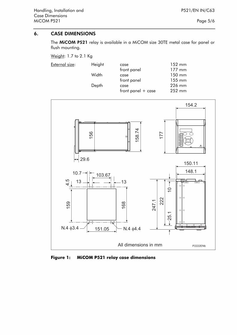
6. CASE DIMENSIONS
The MiCOM P521 relay is available in a MiCOM size 30TE metal case for panel or flush mounting.
Weight: 1.7 to 2.1 Kg
External size: Height case 152 mm front panel 177 mm Width case 150 mm front panel 155 mm Depth case 226 mm front panel + case 252 mm
Figure 1: MiCOM P521 relay case dimensions

P521/EN IN/C63 Handling, Installation and Case Dimensions Page 6/6 MiCOM P521
User Guide P521/EN FT/A83 MiCOM P521
USER GUIDE
Date: 1stOctober 2010
Software version: 12
Connection diagrams: 10P52101

P521/EN FT/A83 User Guide MiCOM P521

User Guide P521/EN FT/A83 MiCOM P521 Page 1/94
CONTENT
1. DESCRIPTION OF THE MiCOM P521 RELAY 5
2. USER INTERFACE 6
2.1 LCD display and keypad description 6
2.1.1 LCD display 6 2.1.2 Keypad 6
2.1.2.1 Alarm keys 6
2.1.2.2 Programming keypad 7
2.2 LEDs 7
2.3 The two areas under the top and bottom flaps 8
2.4 The battery box 9
2.5 Tripping output 9
3. MENUS 9
3.1 Default display 9
3.2 Access to the menu 10
3.3 Password 10
3.3.1 Password protection 10 3.3.2 Entering the password 10
3.3.3 Changing the password 11 3.3.4 Deactivating the password 11
3.4 Alarm display 11
3.4.1 Electrical system alarms 11 3.4.2 Relay hardware or software alarms 14
3.5 Menu contents description 15
3.5.1 OP Parameters menu 16
3.5.2 Configuration menu 18
3.5.2.1 Display sub menu 18
3.5.2.2 CT ratio sub menu 19
3.5.2.3 LED 5 to 8 configuration sub menus 20
3.5.2.4 Group select sub menu 28
3.5.2.5 Alarms sub menu 28
3.5.2.6 Configuration inputs sub menu 29
3.5.2.7 Phase rotation sub menu 30
3.5.3 Measurements menu 31
3.5.3.1 Measurements - Currents Diff sub menu 31
3.5.3.2 Measurements - Current/General sub menu 32

P521/EN FT/A83 User Guide Page 2/94 MiCOM P521
3.5.3.3 Measurements – Protection Comms sub menu 35
3.5.4 Communication menu 36
3.5.4.1 MODBUS communication menu 36
3.5.4.2 IEC 60870-5-103 (VDEW) communication menu 37
3.5.4.3 DNP3.0 communication menu 37
3.5.4.4 Protection communication menu 38
3.5.5 Protection menu 39
3.5.5.1 [87] Current diff sub menu 39
3.5.5.2 [50/51] Phase OC sub menu 43
3.5.5.3 [50N/51N] Earth OC sub menu 46
3.5.5.4 [46] Negative phase sequence I2> sub menu 50
3.5.5.5 [49] Therm OL sub menu 52
3.5.5.6 [37] Undercurrent I< sub menu 53
3.5.6 Automat. ctrl menu 54
3.5.6.1 Commissioning sub menu 54
3.5.6.2 Trip commands sub menu 56
3.5.6.3 Latch functions sub menu 59
3.5.6.4 Blocking logic sub menu 62
3.5.6.5 Logic select sub menus 64
3.5.6.6 Output relays sub menu 65
3.5.6.7 Latch of the auxiliary output relays 71
3.5.6.8 Inversion of the auxiliary output relays 72
3.5.6.9 Inputs sub menu 73
3.5.6.10 Broken conductor sub menu 75
3.5.6.11 Cold load pick-up sub menu 75
3.5.6.12 Circuit breaker failure sub menu 77
3.5.6.13 Circuit breaker supervision sub menu 78
3.5.6.14 Logic Equations 80
3.5.6.15 Program. I-Trip Sub menu 84
3.5.6.16 CT Supervision Sub menu 85
3.5.7 Records menu 86
3.5.7.1 CB monitoring sub menu 87
3.5.7.2 Fault record sub menu 88
3.5.7.3 Instantaneous sub menu 89
3.5.7.4 Disturbance record sub menu 90
3.5.7.5 Time peak value sub menu 91
3.5.7.6 Rolling demand sub menu 91

User Guide P521/EN FT/A83 MiCOM P521 Page 3/94
4. WIRING 93
4.1 Auxiliary supply 93
4.2 Current measurement inputs 93
4.3 Logic inputs 93
4.4 Output relays 93
4.5 Communication 93
4.5.1 EIA(RS)485 rear communication port 93 4.5.2 EIA(RS)232 front communication port 94
FIGURES
FIGURE 1: MICOM P521 FRONT PANEL 6
FIGURE 2: BATTERY BOX MICOM E1 9
FIGURE 3: ORGANIZATION OF MICOM P521 MAIN MENU 15
FIGURE 4: EIA(RS)232 FRONT PORT COMMUNICATION CABLE WIRING 94

P521/EN FT/A83 User Guide Page 4/94 MiCOM P521

User Guide P521/EN FT/A83 MiCOM P521 Page 5/94
1. DESCRIPTION OF THE MiCOM P521 RELAY
MiCOM P521 is a fully numerical relay that is designed to perform electrical protection and control functions.
3 phase and 1 earth current inputs are available at both 1 and 5 Amps ratings on the relay (4 inputs for 1 A and 4 inputs for 5 A). It is possible to use a combination of input ratings on the same relay (i.e. a mix of 1 A for earth fault and 5 A for phase connections).
All output relays can be programmed to respond to any of the available control or protection functions. Logic inputs can also be allocated to the various control functions.
The MiCOM relays are powered from either a DC or an AC auxiliary supply (2 ranges of auxiliary supply). Any short supply interruptions (< 50 ms) are filtered and regulated through the auxiliary supply.
The front panel enables the user to navigate through the menu to access data, change the settings, read the measurements, etc. Eight LEDs on the front panel allows a clear and simple indication of events. The various alarms detected are displayed on the back-lit LCD display. No password is required to read or clear these alarm messages. However, the modification of settings can only be carried out with a password.
MiCOM P521 relay continuously measures the phase and earth currents and calculates the true RMS component up to 10th harmonic.
MiCOM P521 relay has available via its rear connectors, a standard EIA(RS)485 port. Communication protocols can be chosen at the time of order, from MODBUS RTU, IEC 60870-5-103 or DNP3.0. Using the communication channel, all stored information (measurements, alarms and settings) can be read, and the settings can be modified if necessary.
Consultation and modification of this data can be carried out on site with a PC and the appropriate Schneider Electric T&D software (e.g. MiCOM S1 Studio).
EIA(RS)485 based communication allows the MiCOM P521 relay to be directly linked to a digital control system (MiCOM S10 for example). All the available data is then placed at the disposal of the supervisor and can be processed either locally or remotely.
The MiCOM P521 relay gives the user more flexibility to adapt the relay to the desired applications. With regard to low installation costs, this relay offers an economic solution, providing integrated protection and control functions.
P521/EN FT/A83 User Guide Page 6/94 MiCOM P521
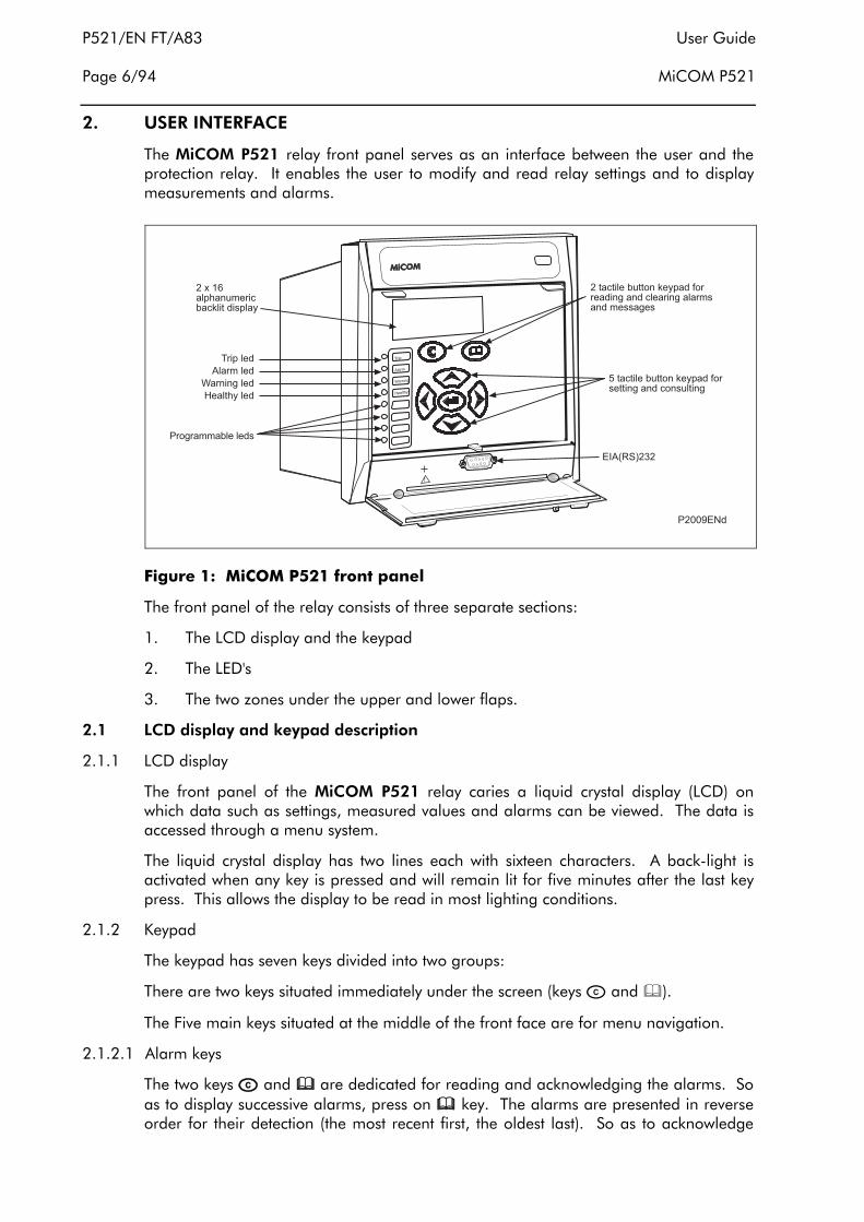
2. USER INTERFACE
The MiCOM P521 relay front panel serves as an interface between the user and the protection relay. It enables the user to modify and read relay settings and to display measurements and alarms.
!"#$%&
''( )
Figure 1: MiCOM P521 front panel
The front panel of the relay consists of three separate sections:
1. The LCD display and the keypad
2. The LED's
3. The two zones under the upper and lower flaps.
2.1 LCD display and keypad description
2.1.1 LCD display
The front panel of the MiCOM P521 relay caries a liquid crystal display (LCD) on which data such as settings, measured values and alarms can be viewed. The data is accessed through a menu system.
The liquid crystal display has two lines each with sixteen characters. A back-light is activated when any key is pressed and will remain lit for five minutes after the last key press. This allows the display to be read in most lighting conditions.
2.1.2 Keypad
The keypad has seven keys divided into two groups:
There are two keys situated immediately under the screen (keys and ).
The Five main keys situated at the middle of the front face are for menu navigation.
2.1.2.1 Alarm keys
The two keys and are dedicated for reading and acknowledging the alarms. So as to display successive alarms, press on key. The alarms are presented in reverse order for their detection (the most recent first, the oldest last). So as to acknowledge
User Guide P521/EN FT/A83 MiCOM P521 Page 7/94
the alarms, the user can either acknowledge each alarm using or go to the end of the ALARM menu and carry out a general acknowledgement.
Latched indications/contacts will also be reset once the key has been pressed.
2.1.2.2 Programming keypad
The five keys situated in the middle of the MiCOM front panel are dedicated to menu navigation and setting changes.
The keys , , and make it possible to move in the direction indicated to the various levels of the menus.
The key validates a choice or value (modification of settings).
2.2 LEDs
The LED labels on the front panel are by default written in English, however the user also has self-adhesive labels, available with MiCOM relays, in French. Additional blank labels are provided on which it is possible to write using a ball point pen.
The top four LEDs indicate to the status of the relay (Trip condition, alarm LED, equipment failure and auxiliary supply).
The four lower LEDs can be freely programmed by the user to correspond to operation of the various thresholds and / or the state of the logic inputs.
Eight LEDs are located in the left portion of the front plate (numbered from 1 to 8 starting from the top):
LED 1 Color : RED Label : Trip
LED 1 indicates when a trip order has been issued by the relay to the circuit breaker or contactor. This LED copies the trip order issued to the Trip output (output RELAY 1). Its normal state is unlit. It is illuminated as soon as a tripping order is issued. It goes out when the associated alarm is acknowledged, provided the initiating protection element has fully reset.
LED 2 Color : ORANGE Label : ALARM
LED 2 indicates that an alarm has been registered by MiCOM P521 relay. The alarms are either threshold crossings (instantaneous), or tripping orders (possibly time delayed, depending upon which protection element operates). In addition to threshold crossings and trips an alarm will also be given in the event of a protection comms channel failure. As soon as an alarm is registered, the LED flashes. When all the stored alarms are read ( ), the LED is illuminated continuously.
When all the alarms are acknowledged , the LED goes out.
Note: The instantaneous alarms can be selected to manual or automatic reset. This can be set in CONFIGURATION/ALARMS/Inst. Self Reset? YES / NO
Choose YES for automatic reset. The default setting is NO.
LED 3 Color : ORANGE Label : Warning
LED 3 is dedicated to the internal alarms of the MiCOM P521. When a « non critical » internal alarm (typically a control comms fault i.e. MODBUS etc.) is detected, the LED will flash. When the fault is classed as « critical », the LED is illuminated continuously. The extinction of this LED is only possible by the disappearance of the cause that provoked it (repair of the module, disappearance of the Fault).
P521/EN FT/A83 User Guide Page 8/94 MiCOM P521
LED 4 Color : GREEN Label : Healthy
LED 4 indicates that the MiCOM P521 has a healthy auxiliary supply in the nominal range.
LED 5 to 8 Color : RED Label : Left Blank
These LEDs can be programmed by the user on the basis of information on available thresholds (instantaneous and time-delayed) and the state of the logic inputs. The user selects the information he wishes to see associated with each LED from the menu element. A single LED can be associated with more than one protection / control function. Each LED illuminates when the associated information is valid. The extinction of each LED occurs when the associated alarm is acknowledged.
2.3 The two areas under the top and bottom flaps
Under the upper flap, a label identifies the relay according to its model (ordering code) and serial number. This information defines the product uniquely and specifically.
In making all requests for information from Schneider Electric T&D After Sales Department, please quote these two numbers.
Information indicated in the lower portion of this label covers the auxiliary supply voltage and the nominal earth current value.
Under the lower flap, an EIA(RS)232 port is available. This can be used to download a setting file from a PC with the MiCOM S1 setting software. Alternatively, the EIA(RS)232 port can be used to download new application software versions into the relay flash memory.
The removal of the MiCOM active part (chassis) from the case is performed by opening the two flaps, then with a 3 mm screwdriver, turn the extractor cam situated under the upper flap, and pull using the two slots situated behind these flaps.
Note: When re-inserting the chassis into the case, ensure that the extractor cam is pushed back flat, and that the chassis is then pushed fully back into the case as far as it can go.

User Guide P521/EN FT/A83 MiCOM P521 Page 9/94
2.4 The battery box
Battery Box MiCOM E 1
To MiCOM EIA(RS)232
Input for external supply12V dc - 24V dc
P0005ENc
Figure 2: Battery box MiCOM E1
The battery box performs the two following functions:
1. Temporary powering of the relay in order to allow the user to view or modify data when the auxiliary power supply has failed. The battery box uses a 6LR61 (9 V) battery, which can power the relay up to 3 hours. When the battery is flat it is possible to power the battery box with an external dc supply. The dc voltage value must be between 12 Vdc and 24 Vdc.
2. EIA(RS)232 interface between the MiCOM relay and the PC equipped with the setting software MiCOM S1 Studio.
2.5 Tripping output
The trip output for the MiCOM P521 relay is dedicated to output relay RL1. Operation of only RL1 will result in illumination of the red trip LED.
3. MENUS
The menu of the MiCOM P521 relay is organized into main and sub menus, much like a PC directory structure.
3.1 Default display
By default, the current value (selected phase, earth or all phases and earth) is continuously displayed.
As soon as an alarm is generated by the MiCOM relay, that information is considered as priority and replaces the default value.
The default display choice is made in the CONFIGURATION/Display menu.

P521/EN FT/A83 User Guide Page 10/94 MiCOM P521
3.2 Access to the menu
Complete menu access is performed by manipulation of the keys , , and . The general arrangement of the menus is shown in Figure 3 for P521.
Reading of parameters and measurements is possible without entering the password. However, modification of the parameters does require the password. Should an error be made in entering a parameter, press to cancel.
Except for reading and canceling, the keys and are inactive.
Note: The letter P is displayed when the password is entered. However If no key is pressed for 5 minutes, the password mode becomes inactive.
3.3 Password
3.3.1 Password protection
Password protection is applicable to the relay settings, especially to the selection of the various thresholds, time delays, communication parameters, allocation of inputs and outputs relays.
The password consists of four alphabetical capital characters. When leaving the factory, the password is AAAA. If necessary the user can define their own combination of characters.
Should the password be lost or forgotten, modification of the relay settings is prohibited. In these circumstances the manufacturer or agent can supply a “master” password when given the relay serial number.
Note: The programming mode is indicated by a letter "P" on the lower right hand side of the display, but only when a column heading is displayed. The letter “P” is present as long as the password is active (5 minutes if no key is pressed).
3.3.2 Entering the password
The password is requested as soon as an attempt is made to modify a relay setting. The user must enter the password (4 characters/letters) and accept the entire password with . If the password is correct “PASSWORD OK” is displayed and setting changes can then commence. If the password is incorrect “PASSWORD NOK” displayed.
After 5 seconds, the display returns to the cell prior to password entry.
If no action is taken on the keypad for 5 minutes, the password is deactivated. A new request shall be associated with any subsequent setting change. A temporary interruption in the auxiliary supply will also serve to de-activate the password.
Note: If the password has been entered via the keypad, the following remote access is possible:
Front port - None
Rear port - Read access only
The relay will remain in this state until the password has been deactivated.
User Guide P521/EN FT/A83 MiCOM P521 Page 11/94
3.3.3 Changing the password
To change the active password, go to the OP. PARAMETERS menu and then to the point of the “Password” sub menu. Enter the old password and validate. Then press and enter the new password character by character and validate the new password using
.
The message “NEW PASSWORD OK” is displayed to indicate that the password has changed.
3.3.4 Deactivating the password
To deactivate the active password, go to the OP. PARAMETERS menu and then to the point of the “Password” sub menu. Press . Password protection is deactivated, and remote access via all communication ports is reactivated.
3.4 Alarm display
The presence of any alarm is displayed on the LCD. The display of alarm messages has priority over the default current value. As soon as an alarm is detected by the relay (threshold crossing for example), the message is displayed on the MiCOM LCD and the Alarm LED (2nd LED) lights up.
The alarm messages are classed as follows:
⇒ Electrical system alarm message
⇒ Hardware or software fault message from the relay.
3.4.1 Electrical system alarms
Any crossing of a threshold (instantaneous or time delay) generates an "electrical system alarm". The threshold that has been exceeded will be displayed on the LCD together with the phase/phases (A, B or C) involved in the fault.
If several alarms are triggered, they are all stored in their order of appearance the most recent alarm first, the oldest alarm last. Each message is numbered and the total number of messages is shown.
The user can read all the alarm messages using the key without entering the password. The user can then acknowledge the alarm using the key. The alarms can be acknowledged one by one or all of them simultaneously by going to the end of the list and pressing the key.
The management of the ALARM LED is directly linked to the status of the stored alarms.
⇒ If one or several messages are NOT READ and NOT ACKNOWLEDGED, the alarm LED flashes.
⇒ If all the messages have been READ but NOT ACKNOWLEDGED, the alarm LED remains lights up continuously.
⇒ If all the messages have been READ and ACKNOWLEDGED, the alarm LED goes out.
Note: The alarms concerning the instantaneous (start indications) can be selected self reset Yes or No in the CONFIGURATION/Alarms Menu
P521/EN FT/A83 User Guide Page 12/94 MiCOM P521
The different electrical system alarms are described below:
Ι DIFF Differential protection trip
Ιe> 1st stage earth fault pick-up
Ιe>> 2nd stage earth fault pick-up
Ιe>>> 3rd stage earth fault pick-up
Ιe>>>> 4th stage earth fault pick-up
Ι> 1st stage overcurrent pick-up
Ι>> 2nd stage overcurrent pick-up
Ι>>> 3rd stage overcurrent pick-up
Ι>>>> 4th stage overcurrent pick-up
tIe> 1st stage earth fault time delay
tIe>> 2nd stage earth fault time delay
tIe>>> 3rd stage earth fault time delay
tIe>>>> 4th stage earth fault time delay
tI> 1st stage overcurrent time delay
tI>> 2nd stage overcurrent time delay
tI>>> 3rd stage overcurrent time delay
tI>>>> 4th stage overcurrent time delay
THERMAL ALARM Thermal alarm threshold pick-up
THERMAL TRIP Thermal trip threshold pick-up
Ι< Undercurrent element pick-up
tΙ< Undercurrent fault time delay
BRKN COND. Broken conductor indication. Ι2/I1 element pick-up for longer than tBC (breaker fail timer). TBC is settable in the AUTOMAT. CTRL/Broken Cond. Menu.
t AUX 1 t AUX1 time delay
t AUX 2 t AUX2 time delay
CB FAILURE Circuit breaker failure indication (the CB did not trip on tBf time delay) tBF is settable in the AUTOMAT. CTRL/CB Fail menu.
Ι 2> Negative sequence current threshold pick-up (1st stage)
tI 2> Negative sequence current threshold time delay (1st stage)
Ι2>> Negative sequence current threshold pick-up (2nd stage)
tI2>> Negative sequence current threshold time delay (2nd stage)
DIRECT Ι-TRIP Indicates that the relay received and tripped on direct intertrip.
Ι DIFF Ι-TRIP Indicates that the relay has received an intertrip signal from the remote relay that has performed a differential trip.

User Guide P521/EN FT/A83 MiCOM P521 Page 13/94
PERMISSIVE Indicates that the relay has tripped due to a permissive intertrip command.
T operating CB Operating (or tripping) time of the circuit breaker longer than the value set in the AUTOMAT. CTRL/CB Supervision menu.
CB CLOSE FAILURE Closing time of the circuit breaker longer than the value set in the AUTOMAT. CTRL/CB Supervision menu.
CB OPEN NB Number of circuit breaker operation higher that the value set in the AUTOMAT. CTRL/CB Supervision menu.
Sum A n Broken current measured higher than the value set in the AUTOMAT. CTRL/CB Supervision menu.
TRIP CIRCUIT Trip circuit failure. Failure condition present for longer than the supervision timer tSUP, settable in the AUTOMAT. CTRL/CB Supervision menu.
LATCH RELAY A least one relay is latched.
CB CLOSE FAILURE Circuit breaker closing time longer than the value set in the AUTOMAT. CTRL/CB Supervision menu.
COMMS ALARM Differential protection communication channel failure. Back-up protection (e.g. overcurrent) can be enabled in the event of COMMS FAILURE.
Ι DIFF FAIL Indicates that the differential protection is not functioning due to either COMMS FAIL or a hardware fault. Back-up protection may still be functioning.
REM TRIP Indicates that the circuit breaker has been given a remote trip command. A remote trip can be initiated by the front user interface, a logic input or via the remote communications link.
CB STATUS DBΙ This alarm stands for "Circuit Breaker Status Don’t Believe It". In the event when the 52a and 52b contacts are both open or both closed, this alarm will be given after 5 seconds.
LOOPBACK MODE Indicates that the protection communications are looped back on themselves for commissioning purposes. The relay will accept messages from its own address. This mode can be enabled/disabled in the AUTOMAT. CTRL/Commissioning menu.
ISOLATED RELAYS Output relays will not operate for fault conditions but alarms and LED’s function as usual. This mode can be used for commissioning purposes.
DISABLED Ι DIFF Indicates that the current differential protection has been disabled. The current differential protection can be disabled via the relay menu or via a blocking input. Blocking/Disabling either local or remote relays will cause this alarm to be displayed at both ends simultaneously.

P521/EN FT/A83 User Guide Page 14/94 MiCOM P521
3.4.2 Relay hardware or software alarms
Any software or hardware fault of the MiCOM relay generates a "hardware/software alarm". If several alarms are generated they are all stored in their order of appearance. The alarms are displayed in reverse order (the most recent first and the oldest last). Each message is numbered and the total number of messages is indicated below.
The user can read all the alarm messages with the aid of , without entering the password.
The acknowledgement of the relay alarm messages is IMPOSSIBLE if the fault is still present. The alarm can only be acknowledged when the cause of the alarm has disappeared.
The management of the WARNING LED is directly linked to the status of the alarms stored in the memory.
⇒ If the fault is major (the relay cannot perform protection functions), the WARNING LED is continuously illuminated and the watchdog contact will operate.
⇒ If the fault is minor (no influence on the protection and automation function e.g. SCADA communication failure), the WARNING LED flashes. This will not cause operation of the watchdog contact.
Possible Hardware or Software alarm messages:
Major fault
SETTING ERROR: Setting error occurred due to data memory fault
EEPROM ERROR CALIBR.: Calibration memory faulty
CT ERROR: Analogue channel faulty
PROT. COMMS FAIL: Protections comms card faulty
DEFAULT CONFIG.: Factory settings restored due to data memory fault. This message will also be displayed following a firmware upgrade.
Minor fault-
RAM ERROR: RAM supplied by battery faulty
BATTERY FAIL: Battery faulty (flat or not correctly fitted)
Note: The “Battery backed RAM memory” and “Battery failure” alarm messages can be configured to display or not; YES or NO in CONFIGURATION/Alarms menu. If NO is selected an alarm will not be raised in the event of a Battery Fault.
COMM.ERROR: Internal communications faulty
CLOCK ERROR: Real time clock faulty
PROT. COMMS RECOVER: Recovering from transient comms fault (back-up protection available)

User Guide P521/EN FT/A83 MiCOM P521 Page 15/94
3.5 Menu contents description
The menu of the MiCOM P521 relay is divided into 8 sections:
⇒ OP PARAMETERS
⇒ CONFIGURATION
⇒ MEASUREMENTS
⇒ COMMUNICATION
⇒ PROTECTION G1
⇒ PROTECTION G2
⇒ AUTOMAT. CTRL
⇒ RECORDS
To access these menus from the default display use .
To return to the default display from these menus or sub menus press .
Figure 3: Organization of MiCOM P521 main menu
Note: The menu content tables are supplied in the Menu Content Tables section, P521/EN HI.

P521/EN FT/A83 User Guide Page 16/94 MiCOM P521
3.5.1 OP Parameters menu
To gain access to the OP PARAMETERS menu from the default display, press .
OP PARAMETERS Heading of the OP PARAMETERS menu To gain access to the menu content, press .
Password * * * *
Entry of the password to be able to modify the MiCOM relay settings and parameters. To enter the password, press . To deactivate the active password, press .
Password
AAAA
Entry of the password is made letter by letter using and to go up or down the alphabet. After each letter, press
, to enter the following letter. At the end, press to validate the password. If the password is correct, the message « PASSWORD OK » is displayed on the screen. Note: The password is initially set in the factory to AAAA.
WARNING: AS SOON AS THE PASSWORD HAS BEEN ENTERED, NO SETTING CHANGE USING THE COMMUNICATION (EIA(RS)485 OR EIA(RS)232) CAN BE
ACCEPTED.
LANGUAGE =
ENGLISH
Choose the language for HMI. Can be selected from the following: ENGLISH, FRANCAIS, DEFAULT, CHINESE, POLSKI, RUSSIAN, ITALIANO, DEUTSCH and ESPANOL.
Description
P521xxxxxxxxxx
Displays the MiCOM applicable relay model (full code).
SERIAL NUM =
00000001
Displays the serial number of the relay.
Reference
MiCO
Displays the name of the equipment associated with the relay. The entry of the reference is made character by character using , . After each character (letter, number or symbol), press to move to the next character. At the end of entering, press to accept the reference. Note: The reference is initially set in the factory to MiCO.
Software version 12.A
Displays the version of the software.
User Guide P521/EN FT/A83 MiCOM P521 Page 17/94
Frequency 50 Hz
Nominal value of the network frequency. Select either 50 or 60 Hz. To modify this value, press followed by , to select the desired value. Validate your choice using .
Active Group 1
Display the active group (Protection G1 or Protection G2).
Input 54321 Status 10110
Displays the state of the logic Inputs. The Logic Inputs are numbered from 1 to 5, starting from the right. The state of each input is : - state 0 : input inactive - state 1 : input active
Relay 87654321 Status 01011101
Displays the state of the logic outputs. The logic outputs are numbered from 1 to 8, starting from the right. The state of each output is : - state 0 : output relay not operated - state 1 : output relay operated Pressing the cancel key , in this cell, will reset any latched contacts/relays, this is with the exception of trip relay RL1. Note: The Watch-dog output (RL0) is not displayed in the output status menu.
Date 30/01/02
Displays the date. To modify this date press then use , , to enter the required value. Accept your choice using . With this example the date is : 30 January 2002.
Time
13:57:44
Displays the Time. To modify this time press then use , to enter the required value. Accept your choice
using . With this example the time is : 13 hours, 57 minutes, 44 seconds.
Trip and Close
No Operation
Enables the user to Trip or Close the circuit breaker. Select from “No Operation”, “Trip” or “Close”.
To Trip or Close the circuit select either “Trip” or “Close” and then press the key. The relevant output contacts will close for the “Open Pulse” or “t Close Pulse” times found under AUTOMAT. CTRL/CB Monitoring.
Disturb Trigger
No
Enables the user to create a disturbance record manually.
To trigger a disturbance record, press the key and then select “Yes” using , .

P521/EN FT/A83 User Guide Page 18/94 MiCOM P521
3.5.2 Configuration menu
The various sub menus are:
⇒ Display
⇒ CT Ratio
⇒ Led 5
⇒ Led 6
⇒ Led 7
⇒ Led 8
⇒ Group Select
⇒ Alarms
⇒ Configuration Inputs
⇒ Phase Rotation
To gain access to the CONFIGURATION menu from the default display, press then .
3.5.2.1 Display sub menu
CONFIGURATION Heading of the CONFIGURATION menu. To gain access to the DISPLAY submenu, press .
Display Heading of the DISPLAY sub menu. To gain access to the sub menu content, press .
Default Display
RMS I A
Edit the default display to show either Phase A, Phase B, Phase C, Earth currents or all four simultaneously. To modify the default display, press then use either or
to enter the required choice. Enable your choice using .
Phase A Text L1
Edit phase A label by selecting L1, A or R. This value can be modified after entering the password and is displayed with the corresponding measurement.
Phase B Text L2
Edit phase B label by selecting L2, B, S, Y or W. This value can be modified after entering the password and is displayed with the corresponding measurement.
Phase C Text L3
Edit phase C label by selecting L3, C, T or B. This value can be modified after entering the password and is displayed with the corresponding measurement.

User Guide P521/EN FT/A83 MiCOM P521 Page 19/94
E/Gnd Text
E
Edit earth label by selecting N, E, or o. This value can be modified after entering the password and is displayed with the corresponding measurement.
3.5.2.2 CT ratio sub menu
CONFIGURATION Heading of the CONFIGURATION menu. To gain access to the CT RATIOS menu, press , .
CT Ratio Heading of the CT RATIOS sub menu. To gain access to the sub menu content, press .
Line CT primary 1000
Display of the primary rating of the phase CT. The value consists of 4 digits : Minimum 1, Maximum 9999. Press to modify this value and use , , , to display the new primary phase CT ratio. Enable your choice by pressing at the end of selection.
Line CT sec 5
Display of the secondary rating of the phase CT.
This value toggles between 1 and 5.
E/Gnd CT primary 1000
Display of the primary rating of the earth CT. The value consists of 4 digits : Minimum 1, Maximum 9999.
Press to modify this value and use , , , to display the new primary earth CT ratio. Enable your choice by pressing at the end of selection.
E/Gnd CT sec 5
Display of the secondary rating of the earth CT.
This value toggles between 1 and 5.
CT Correct Ratio 1.0
Displays the ratio correction factor that the local current is multiplied by. The correction factor has a setting range of 0.05 to 2.
Press ↵ to modify this value and use ⇑, ⇓, ⇒, ⇐ to display the new correction factor. Enable your choice by pressing ↵ at the end of selection.
Vectorial Comp. Off
Displays the vector group that is in use.
P521/EN FT/A83 User Guide Page 20/94 MiCOM P521
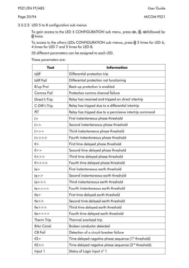
3.5.2.3 LED 5 to 8 configuration sub menus
To gain access to the LED 5 CONFIGURATION sub menu, press , , followed by twice.
To access to the others LEDs CONFIGURATION sub menus, press 3 times for LED 6, 4 times for LED 7 and 5 times for LED 8.
35 different parameters can be assigned to each LED.
These parameters are:
Text Information
Ιdiff Differential protection trip
Ιdiff Fail Differential protection not functioning
B/up Prot Back-up protection is enabled
Comms Fail Protection comms channel failure
Direct Ι-Trip Relay has received and tripped on direct intertrip
C-Diff Ι-Trip Relay has tripped due to a differential intertrip
PIT Relay has tripped due to a permissive intertrip command
Ι> First instantaneous phase threshold
Ι>> Second instantaneous phase threshold
Ι>>> Third instantaneous phase threshold
Ι>>>> Fourth instantaneous phase threshold
tI> First time delayed phase threshold
tI>> Second time delayed phase threshold
tI>>> Third time delayed phase threshold
tI>>>> Fourth time delayed phase threshold
Ιe> First instantaneous earth threshold
Ιe>> Second instantaneous earth threshold
Ιe>>> Third instantaneous earth threshold
Ιe>>>> Fourth instantaneous earth threshold
tIe> First time delayed earth threshold
tIe>> Second time delayed earth threshold
tIe>>> Third time delayed earth threshold
tIe>>>> Fourth time delayed earth threshold
Therm Trip Thermal overload trip
Brkn Cond. Broken conductor detected
CB Fail Detection of a circuit breaker failure
tI2> Time delayed negative phase sequence (1st threshold)
tI2>> Time delayed negative phase sequence (2nd threshold)
Input 1 Status of Logic Input n° 1

User Guide P521/EN FT/A83 MiCOM P521 Page 21/94
Text Information
Input 2 Status of Logic Input n° 2
Input 3 Status of Logic Input n° 3
Input 4 Status of Logic Input n° 4
Input 5 Status of Logic Input n° 5
t Aux 1 Aux Timer 1 operated
t Aux 2 Aux Timer 2 operated
CB Alarm Circuit breaker alarm
Equation A Equation A operated
Equation B Equation B operated
Equation C Equation C operated
Equation D Equation D operated
Equation E Equation E operated
Equation F Equation F operated
Equation G Equation G operated
Equation H Equation H operated
Prgm IT 1 Programmable Inter-trip 1 operated
Prgm IT 2 Programmable Inter-trip 2 operated
Prgm IT 3 Programmable Inter-trip 3 operated
Prgm IT 4 Programmable Inter-trip 4 operated
CTS Local Local CT failure detected
CTS Remote Remote end CT failure detected
CTS Block CT failure is detected and relevant protections are blocked (undercurrent, negative sequence overcurrent, broken conductor).
CTS Restrain CT failure is detected and differential protection is in Restraint mode.
Convention
Mode
Protection communication uses convention mode, i.e., not extended with the functions of CTS and Programmable Inter-trip.
CDiff Disabled Current differential protection is disabled.
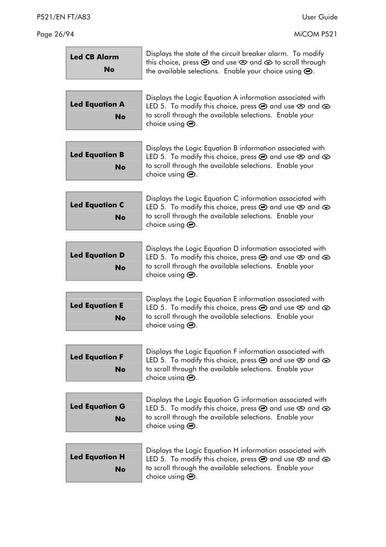
Notes: ⇒ Each parameter can be assigned to one or more LED's. ⇒ Each LED can be lit by one or more parameters (OR logic).
Example of LED 5 setting:
CONFIGURATION Heading of the CONFIGURATION menu. To gain access to the LED 5 submenu, press , followed by 2 times.

P521/EN FT/A83 User Guide Page 22/94 MiCOM P521
Led 5 Heading of the LED 5 sub menu. To gain access to the sub menu content, press .
Led Idiff
No
Indicates that the differential protection has tripped. To modify this choice, press and use and to scroll through the available selections. Enable your choice using
.
Led Idiff Fail
No
Indicates that the differential protection is not functioning. To modify this choice, press and use and to scroll through the available selections. Enable your choice using
.
Led B/up Prot
No
Displays that the back-up protection has been enabled. To modify this choice, press and use and to scroll through the available selections. Enable your choice using
.
Led Comms Fail
No
Indicates that the protection comms channel has failed. To modify this choice, press and use and to scroll through the available selections. Enable your choice using
.
Led Direct
I-Trip No
Indicates that the relay has received and tripped on a direct intertrip. To modify this choice, press and use and
to scroll through the available selections. Enable your choice using .
Led C-Diff
I-Trip No
Indicates that the relay has tripped due to a differential intertrip. To modify this choice, press and use and
to scroll through the available selections. Enable your choice using .
Led PIT
No
Indicates that the relay has tripped due to a permissive intertrip command. To modify this choice, press and use
and to scroll through the available selections. Enable your choice using .
Led I> No
Displays the instantaneous threshold I> associated with LED 5. To modify this choice, press and use and to scroll through the available selections. Enable your choice using .

User Guide P521/EN FT/A83 MiCOM P521 Page 23/94
Led tI> No
Displays the time delay threshold tI> associated with LED 5. To modify this choice, press and use and to scroll through the available selections. Enable your choice using
.
Led I>> No
Displays the instantaneous threshold I>> associated with LED 5. To modify this choice, press and use and to scroll through the available selections. Enable your choice using .
Led tI>> No
Displays the time delay threshold tI>> associated with LED 5. To modify this choice, press and use and to scroll through the available selections. Enable your choice using .
Led I>>> No
Displays the instantaneous threshold I>>> associated with LED 5. To modify this choice, press and use and to scroll through the available selections. Enable your choice using .
Led tI>>> No
Displays the time delay threshold tI>>> associated with LED 5. To modify this choice, press and use and to scroll through the available selections. Enable your choice using .
Led I>>>> No
Displays the instantaneous threshold I>>>> associated with LED 5. To modify this choice, press and use and
to scroll through the available selections. Enable your choice using .
Led tI>>>> No
Displays the time delay threshold tI>>>> associated with LED 5. To modify this choice, press and use and to scroll through the available selections. Enable your choice using .
Led Ie> No
Displays the instantaneous threshold Ie> associated with LED 5. To modify this choice, press and use and to scroll through the available selections. Enable your choice using .
Led tIe> No
Displays the time delay threshold tIe> associated with LED 5. To modify this choice, press and use and to scroll through the available selections. Enable your choice using .

P521/EN FT/A83 User Guide Page 24/94 MiCOM P521
Led Ie>> No
Displays the instantaneous threshold Ie>> associated with LED 5. To modify this choice, press and use and
to scroll through the available selections. Enable your choice using .
Led tIe>> No
Displays the time delay threshold tIe>> associated with LED 5. To modify this choice, press and use and to scroll through the available selections. Enable your choice using .
Led Ie>>> No
Displays the instantaneous threshold Ie>>> associated with LED 5. To modify this choice, press and use and to scroll through the available selections. Enable your choice using .
Led tIe>>> No
Displays the time delay threshold tIe>>> associated with LED 5. To modify this choice, press and use and to scroll through the available selections. Enable your choice using .
Led Ie>>>> No
Displays the instantaneous threshold Ie>>>> associated with LED 5. To modify this choice, press and use and
to scroll through the available selections. Enable your choice using .
Led tIe>>>> No
Displays the time delay threshold tIe>>>> associated with LED 5. To modify this choice, press and use and to scroll through the available selections. Enable your choice using .
Led Therm
Trip No
Displays the thermal threshold tIθ trip order associated with LED 5. To modify this choice, press and use and to scroll through the available selections. Enable your choice using .
Led Brkn. Cond
No
Displays the broken conductor information associated with LED 5. To modify this choice, press and use and to scroll through the available selections. Enable your choice using .
Led CB Fail
No
Displays the circuit breaker failure information associated with LED 5. To modify this choice, press and use and
to scroll through the available selections. Enable your choice using .

User Guide P521/EN FT/A83 MiCOM P521 Page 25/94
Led tI2>
No
Displays the negative phase sequence 1st threshold tI2> associated with LED 5. To modify this choice, press and use and to scroll through the available selections. Enable your choice using .
Led tI2>>
No
Displays the negative phase sequence 2nd threshold tI2>> associated with LED 5. To modify this choice, press and use and to scroll through the available selections. To this LED. Enable your choice using .
Led Input 1
No
Displays the state of the logic input 1 associated with LED 5. To modify this choice, press and use and to scroll through the available selections. Enable your choice using
.
Led Input 2
No
Displays the state of the logic input 2 associated with LED 5. To modify this choice, press and use and to scroll through the available selections. Enable your choice using
.
Led Input 3
No
Displays the state of the logic input 3 associated with LED 5. To modify this choice, press and use and to scroll through the available selections. Enable your choice using
.
Led Input 4
No
Displays the state of the logic input 4 associated with LED 5. To modify this choice, press and use and to scroll through the available selections. Enable your choice using
.
Led Input 5
No
Displays the state of the logic input 5 associated with LED 5. To modify this choice, press and use and to scroll through the available selections. Enable your choice using
.
Led t Aux 1
No
Displays the state of the logic input delayed by t Aux 1. To modify this choice, press and use and to scroll through the available selections. Enable your choice using
.
Led t Aux 2
No
Displays the state of the logic input delayed by t Aux 2. To modify this choice, press and use and to scroll through the available selections. Enable your choice using
.
P521/EN FT/A83 User Guide Page 26/94 MiCOM P521
Led CB Alarm
No
Displays the state of the circuit breaker alarm. To modify this choice, press and use and to scroll through the available selections. Enable your choice using .
Led Equation A
No
Displays the Logic Equation A information associated with LED 5. To modify this choice, press and use and to scroll through the available selections. Enable your choice using .
Led Equation B
No
Displays the Logic Equation B information associated with LED 5. To modify this choice, press and use and to scroll through the available selections. Enable your choice using .
Led Equation C
No
Displays the Logic Equation C information associated with LED 5. To modify this choice, press and use and to scroll through the available selections. Enable your choice using .
Led Equation D
No
Displays the Logic Equation D information associated with LED 5. To modify this choice, press and use and to scroll through the available selections. Enable your choice using .
Led Equation E
No
Displays the Logic Equation E information associated with LED 5. To modify this choice, press and use and to scroll through the available selections. Enable your choice using .
Led Equation F
No
Displays the Logic Equation F information associated with LED 5. To modify this choice, press and use and to scroll through the available selections. Enable your choice using .
Led Equation G
No
Displays the Logic Equation G information associated with LED 5. To modify this choice, press and use and to scroll through the available selections. Enable your choice using .
Led Equation H
No
Displays the Logic Equation H information associated with LED 5. To modify this choice, press and use and to scroll through the available selections. Enable your choice using .
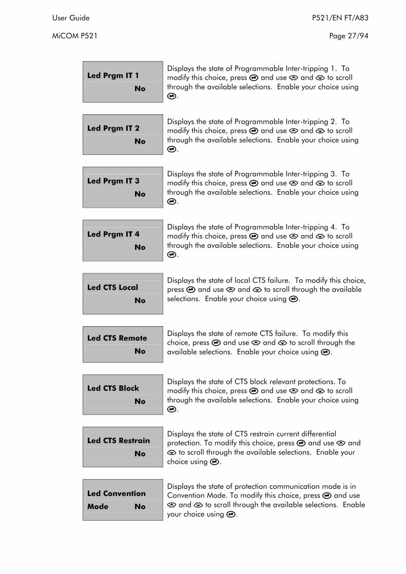
User Guide P521/EN FT/A83 MiCOM P521 Page 27/94
Led Prgm IT 1
No
Displays the state of Programmable Inter-tripping 1. To modify this choice, press and use and to scroll through the available selections. Enable your choice using
.
Led Prgm IT 2
No
Displays the state of Programmable Inter-tripping 2. To modify this choice, press and use and to scroll through the available selections. Enable your choice using
.
Led Prgm IT 3
No
Displays the state of Programmable Inter-tripping 3. To modify this choice, press and use and to scroll through the available selections. Enable your choice using
.
Led Prgm IT 4
No
Displays the state of Programmable Inter-tripping 4. To modify this choice, press and use and to scroll through the available selections. Enable your choice using
.
Led CTS Local
No
Displays the state of local CTS failure. To modify this choice, press and use and to scroll through the available selections. Enable your choice using .
Led CTS Remote
No
Displays the state of remote CTS failure. To modify this choice, press and use and to scroll through the available selections. Enable your choice using .
Led CTS Block
No
Displays the state of CTS block relevant protections. To modify this choice, press and use and to scroll through the available selections. Enable your choice using
.
Led CTS Restrain
No
Displays the state of CTS restrain current differential protection. To modify this choice, press and use and
to scroll through the available selections. Enable your choice using .
Led Convention
Mode No
Displays the state of protection communication mode is in Convention Mode. To modify this choice, press and use
and to scroll through the available selections. Enable your choice using .

P521/EN FT/A83 User Guide Page 28/94 MiCOM P521
3.5.2.4 Group select sub menu
CONFIGURATION Heading of the CONFIGURATION menu. To gain access to the menu, press , , , followed by ⇒ 6 times.
Group Select Heading of the GROUP SELECT sub menu. To gain access to the sub menu content, press .
Change Group Input = EDGE
Displays the operation mode of the digital input associated to the change of protection setting group: "EDGE" or "LEVEL". To change the operation mode, press then use and
to scroll through the available selections. Enable your choice using .
Setting Group 1
Displays of the active setting group (1 or 2). To manually change the active setting group, press then use and
to enter the required value (1 or 2). Enable your choice using . Manual changes are only possible if “EDGE” is selected in the previous cell
3.5.2.5 Alarms sub menu
CONFIGURATION Heading of the configuration menu. To gain access to alarms menu, press , , , followed by ⇒ 7 times.
Alarms Heading of the alarms sub menu. To gain access to the sub menu content, press .
Inst. Self-reset? No
Displays the reset mode of the alarms concerning the instantaneous (protection start indications): self-reset Yes or No. If the user chooses No, the reset must be done by the push button. To change the reset mode press then use
and to select either Yes or No. Enable your choice using .
Comm.Fail-reset? No
Displays the reset mode of the Communication Failure alarm: self-reset Yes or No. If the user chooses No, the reset must be done by the push button. If the user chooses Yes, the Communication Failure alarm will automatically reset when the protection communication is re-established. To change the reset mode press then use and to select either Yes or No. Enable your choice using .

User Guide P521/EN FT/A83 MiCOM P521 Page 29/94
CDiff Disabled
Alarm? No
Select the mode of alarm displaying when the Current Differential is disabled. If Yes is chosen, Alarm will be raised when differential protection is disabled. Otherwise alarm will not be raised. To change the setting press then use and to select either Yes or No. Enable your choice using
.
3.5.2.6 Configuration inputs sub menu
It is possible to configure individual digital inputs to be active from either a falling edge/low level, or on a rising edge/high level. This can be done using the “inputs” cell in the “CONFIGURATION” column A “0” means that the opto is active low, if the associated function is LEVEL dependent, or active for a falling edge if EDGE dependent. Conversely, a “1” means that the opto is active high, if the associated function is LEVEL dependent, or active for a rising edge if EDGE dependent. The choice of how the digital inputs are activated is dependent upon the application.
The table below shows which functions are LEVEL or EDGE dependent.
Example: a digital input configured "blocking logic" will operate on level, on the other hand a digital input configured "cold load pick up" will operate on edge.
ONLY a digital input configured "change of setting group" can operate either on edge or on level (selectable).
Function allocated to the Digital Input Operation of the Digital Input
Unlatch of the output relays On level
Position of the CB, 52a or 52b On level
Blocking logic 1 & 2 On level
Logic selectivity 1 & 2 On level
Aux 1 & Aux 2 On level
CB fault On level
Reset of the thermal state On edge
Blocking of the auto-recluse On level
Cold load pick up On edge
Start of disturbance record On edge
Trip circuit supervision On level
Change of setting group On edge or on level
CB fail start On edge
The user has to set in the CONFIGURATION Menu the auxiliary voltage (AC or DC) for the operation of the digital inputs. This setting is necessary due to the time filtering being different if DC or AC is chosen.
CONFIGURATION Heading of the CONFIGURATION menu. To gain access to Configuration Inputs menu, press , , , followed by 8 times.

P521/EN FT/A83 User Guide Page 30/94 MiCOM P521
Configuration Inputs
Heading of the Configuration Inputs sub menu. To gain access to the sub menu content, press .
Inputs 5 4 3 2 1 1 1 1 1 1
Displays how the digital Inputs are activated either on a falling edge/low level, or on a rising edge/high level: 0 = falling edge/low level 1 = rising edge/high level To change the operation mode press then use , to highlight each input followed by and to toggle between 0 and 1. Enable your choice using .
Voltage input =
DC
Displays the voltage (AC or DC) on the digital Inputs. To change the voltage press then use and to toggle between AC or DC. Enable your choice using .
3.5.2.7 Phase rotation sub menu
CONFIGURATION
Heading of the CONFIGURATION menu. To gain access to the Phase rotation menu, press , , , followed by 9 times.
Phase Rotation Heading of the PHASE ROTATION sub menu. To gain access to the Phase Rotation menu, press .
Phase Rotation A-B-C
Displays the phase rotation either A-B-C or A-C-B. To change the phase rotation press then use and to toggle between A-B-C or A-C-B. Enable your choice using
.
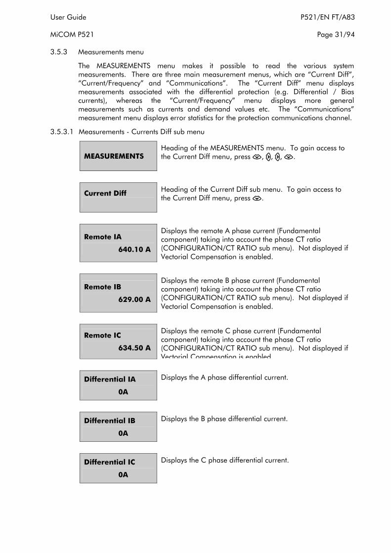
User Guide P521/EN FT/A83 MiCOM P521 Page 31/94
3.5.3 Measurements menu
The MEASUREMENTS menu makes it possible to read the various system measurements. There are three main measurement menus, which are “Current Diff”, “Current/Frequency” and “Communications”. The “Current Diff” menu displays measurements associated with the differential protection (e.g. Differential / Bias currents), whereas the “Current/Frequency” menu displays more general measurements such as currents and demand values etc. The “Communications” measurement menu displays error statistics for the protection communications channel.
3.5.3.1 Measurements - Currents Diff sub menu
MEASUREMENTS Heading of the MEASUREMENTS menu. To gain access to the Current Diff menu, press , , , .
Current Diff
Heading of the Current Diff sub menu. To gain access to the Current Diff menu, press .
Remote IA
640.10 A
Displays the remote A phase current (Fundamental component) taking into account the phase CT ratio (CONFIGURATION/CT RATIO sub menu). Not displayed if Vectorial Compensation is enabled.
Remote IB
629.00 A
Displays the remote B phase current (Fundamental component) taking into account the phase CT ratio (CONFIGURATION/CT RATIO sub menu). Not displayed if Vectorial Compensation is enabled.
Remote IC
634.50 A
Displays the remote C phase current (Fundamental component) taking into account the phase CT ratio (CONFIGURATION/CT RATIO sub menu). Not displayed if Vectorial Compensation is enabled
Differential IA
0A
Displays the A phase differential current.
Differential IB
0A
Displays the B phase differential current.
Differential IC
0A
Displays the C phase differential current.
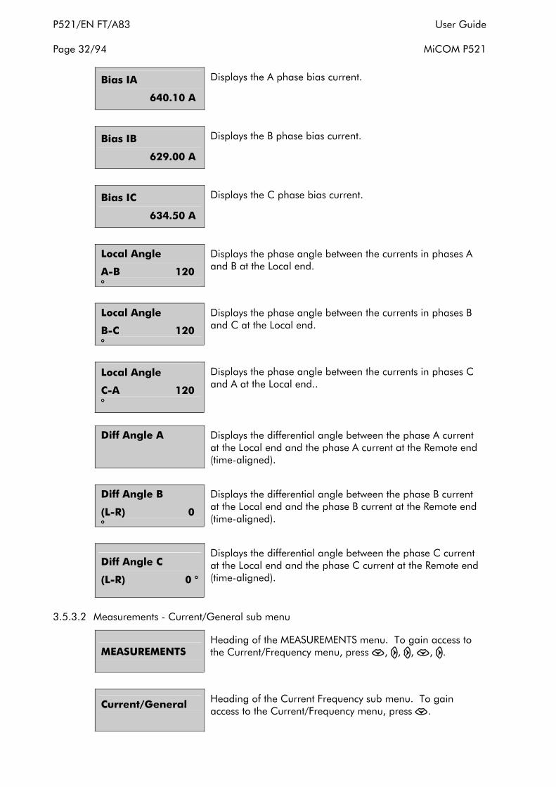
P521/EN FT/A83 User Guide Page 32/94 MiCOM P521
Bias IA
640.10 A
Displays the A phase bias current.
Bias IB
629.00 A
Displays the B phase bias current.
Bias IC
634.50 A
Displays the C phase bias current.
Local Angle
A-B 120 °
Displays the phase angle between the currents in phases A and B at the Local end.
Local Angle
B-C 120 °
Displays the phase angle between the currents in phases B and C at the Local end.
Local Angle
C-A 120 °
Displays the phase angle between the currents in phases C and A at the Local end..
Diff Angle A Displays the differential angle between the phase A current at the Local end and the phase A current at the Remote end (time-aligned).
Diff Angle B
(L-R) 0 °
Displays the differential angle between the phase B current at the Local end and the phase B current at the Remote end (time-aligned).
Diff Angle C
(L-R) 0 °
Displays the differential angle between the phase C current at the Local end and the phase C current at the Remote end (time-aligned).
3.5.3.2 Measurements - Current/General sub menu
MEASUREMENTS Heading of the MEASUREMENTS menu. To gain access to the Current/Frequency menu, press , , , , .
Current/General
Heading of the Current Frequency sub menu. To gain access to the Current/Frequency menu, press .

User Guide P521/EN FT/A83 MiCOM P521 Page 33/94
I A
640.10 A
Displays the A phase current (True RMS value) taking into account the phase CT ratio (CONFIGURATION/CT RATIO sub menu).
I B
629.00 A
Displays the B phase current (True RMS value) taking into account the phase CT ratio (CONFIGURATION/CT RATIO sub menu).
I C
634.50 A
Displays the C phase current (True RMS value) taking into account the phase CT ratio (CONFIGURATION/CT RATIO sub menu).
I N
3.15 A
Displays the earth current (True RMS value) taking into account the earth CT ratio (CONFIGURATION/CT RATIO sub menu).
I1 =
103A
Displays the positive sequence current.
I2 =
50A
Displays the negative sequence current.
RATIO I2/I1 =
50%
Displays the ratio of I2/I1.
I N - fn RST = [C] 0.0A
Displays the earth current (True RMS value) minus the current value at the fundamental frequency (value of the harmonics). To clear the value, press (password needed).
Thermal θ RST = [C] 67%
Displays the % thermal state based on true RMS values. To clear the % values, press (password needed).
Max & Average I RST = [C]
Allows the user to clear the maximum (peak) and average (rolling) memorized values of the current. To clear these values, press (password needed).
Max IA Rms
127.36 A
Displays the maximum (peak) value for phase A. The value is the true RMS maximum value.
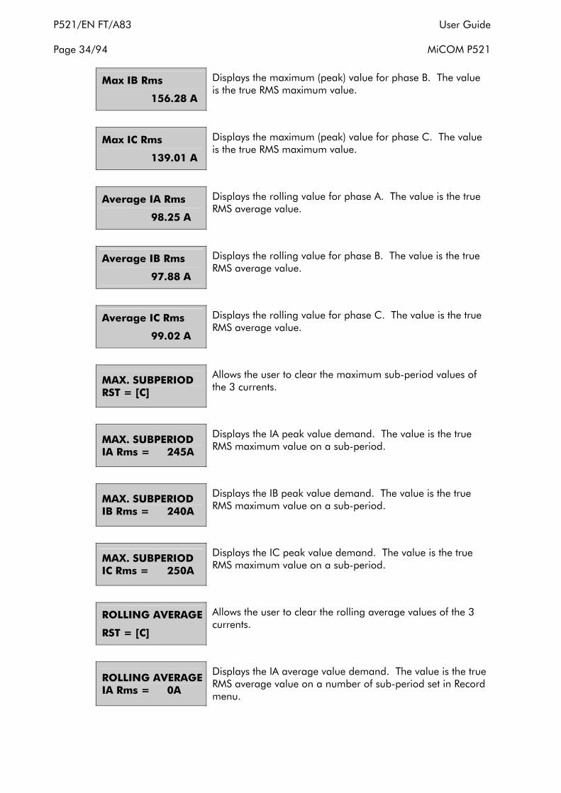
P521/EN FT/A83 User Guide Page 34/94 MiCOM P521
Max IB Rms
156.28 A
Displays the maximum (peak) value for phase B. The value is the true RMS maximum value.
Max IC Rms
139.01 A
Displays the maximum (peak) value for phase C. The value is the true RMS maximum value.
Average IA Rms
98.25 A
Displays the rolling value for phase A. The value is the true RMS average value.
Average IB Rms
97.88 A
Displays the rolling value for phase B. The value is the true RMS average value.
Average IC Rms
99.02 A
Displays the rolling value for phase C. The value is the true RMS average value.
MAX. SUBPERIOD RST = [C]
Allows the user to clear the maximum sub-period values of the 3 currents.
MAX. SUBPERIOD IA Rms = 245A
Displays the IA peak value demand. The value is the true RMS maximum value on a sub-period.
MAX. SUBPERIOD IB Rms = 240A
Displays the IB peak value demand. The value is the true RMS maximum value on a sub-period.
MAX. SUBPERIOD IC Rms = 250A
Displays the IC peak value demand. The value is the true RMS maximum value on a sub-period.
ROLLING AVERAGE
RST = [C]
Allows the user to clear the rolling average values of the 3 currents.
ROLLING AVERAGE IA Rms = 0A
Displays the IA average value demand. The value is the true RMS average value on a number of sub-period set in Record menu.
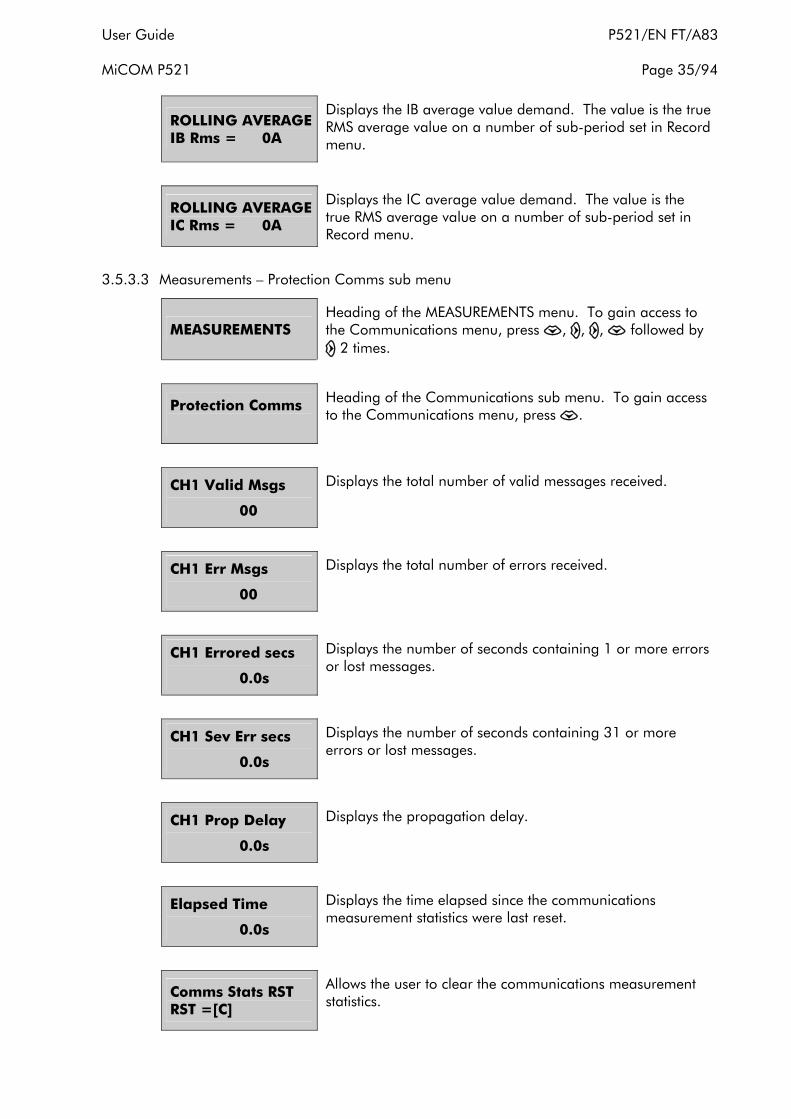
User Guide P521/EN FT/A83 MiCOM P521 Page 35/94
ROLLING AVERAGE IB Rms = 0A
Displays the IB average value demand. The value is the true RMS average value on a number of sub-period set in Record menu.
ROLLING AVERAGE IC Rms = 0A
Displays the IC average value demand. The value is the true RMS average value on a number of sub-period set in Record menu.
3.5.3.3 Measurements – Protection Comms sub menu
MEASUREMENTS Heading of the MEASUREMENTS menu. To gain access to the Communications menu, press , , , followed by
2 times.
Protection Comms
Heading of the Communications sub menu. To gain access to the Communications menu, press .
CH1 Valid Msgs
00
Displays the total number of valid messages received.
CH1 Err Msgs
00
Displays the total number of errors received.
CH1 Errored secs
0.0s
Displays the number of seconds containing 1 or more errors or lost messages.
CH1 Sev Err secs
0.0s
Displays the number of seconds containing 31 or more errors or lost messages.
CH1 Prop Delay
0.0s
Displays the propagation delay.
Elapsed Time
0.0s
Displays the time elapsed since the communications measurement statistics were last reset.
Comms Stats RST RST =[C]
Allows the user to clear the communications measurement statistics.

P521/EN FT/A83 User Guide Page 36/94 MiCOM P521
3.5.4 Communication menu
There are two sub-menus under the COMMUNICATION menu: Ctrl Comms and Protection.
The Ctrl Comms sub-menu contains the configuration parameters for the rear EIA(RS)485 communication port, which depend on the protocol (order option): MODBUS, IEC 60870-5-103 or DNP3.0.
The Protection sub-menu contains the configuration parameters for the protection signaling interface to the remote P521.
3.5.4.1 MODBUS communication menu
COMMUNICATION Heading of the COMMUNICATION menu. To gain access to the Control Comms menu, press , 3 times then . To gain access to the sub menu points, press .
Ctrl Comms Heading of the Control Comms menu. To gain access to the Control Comms menu press .
Ctrl Comms?
Yes
Enables / disables MODBUS RTU communication via the EIA(RS)485 port on the rear of the relay. To activate communications, press the key and use to select Yes. Enable your choice using .
Baud Rate
19200 bd
Displays the speed of the MODBUS transmission. Select from: 300, 600, 1200, 2400, 4800, 9600, 19200, 38400 bauds using or and enable your choice using .
Parity
None
Displays the parity in the MODBUS frame. Select Even, Odd or None using or and enable your choice using .
Stop bits
1
Displays the number of stop bits in the MODBUS frame. Select 1 or 2 using or and enable your choice using
.
Relay Address
1
Displays the network address of the MiCOM relay in the MODBUS network. Select from 1 to 255 using or and enable your choice using .
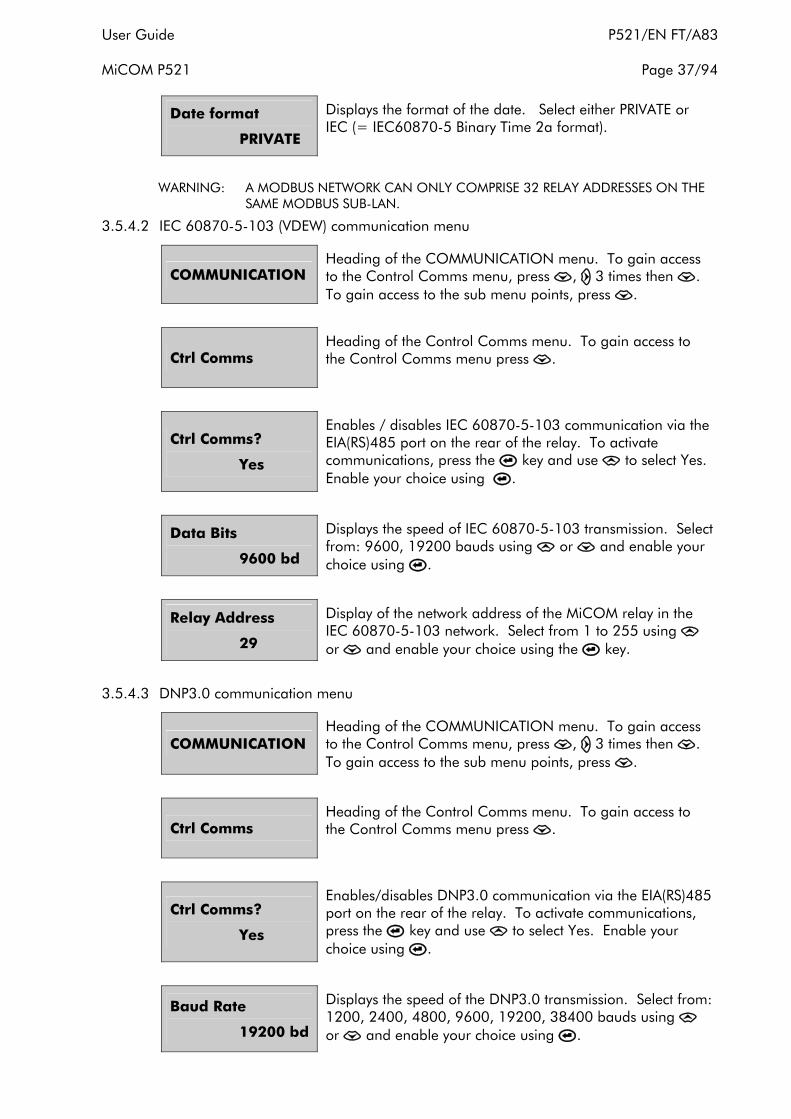
User Guide P521/EN FT/A83 MiCOM P521 Page 37/94
Date format
PRIVATE
Displays the format of the date. Select either PRIVATE or IEC (= IEC60870-5 Binary Time 2a format).
WARNING: A MODBUS NETWORK CAN ONLY COMPRISE 32 RELAY ADDRESSES ON THE
SAME MODBUS SUB-LAN.
3.5.4.2 IEC 60870-5-103 (VDEW) communication menu
COMMUNICATION Heading of the COMMUNICATION menu. To gain access to the Control Comms menu, press , 3 times then . To gain access to the sub menu points, press .
Ctrl Comms Heading of the Control Comms menu. To gain access to the Control Comms menu press .
Ctrl Comms?
Yes
Enables / disables IEC 60870-5-103 communication via the EIA(RS)485 port on the rear of the relay. To activate communications, press the key and use to select Yes. Enable your choice using .
Data Bits
9600 bd
Displays the speed of IEC 60870-5-103 transmission. Select from: 9600, 19200 bauds using or and enable your choice using .
Relay Address
29
Display of the network address of the MiCOM relay in the IEC 60870-5-103 network. Select from 1 to 255 using or and enable your choice using the key.
3.5.4.3 DNP3.0 communication menu
COMMUNICATION Heading of the COMMUNICATION menu. To gain access to the Control Comms menu, press , 3 times then . To gain access to the sub menu points, press .
Ctrl Comms Heading of the Control Comms menu. To gain access to the Control Comms menu press .
Ctrl Comms?
Yes
Enables/disables DNP3.0 communication via the EIA(RS)485 port on the rear of the relay. To activate communications, press the key and use to select Yes. Enable your choice using .
Baud Rate
19200 bd
Displays the speed of the DNP3.0 transmission. Select from: 1200, 2400, 4800, 9600, 19200, 38400 bauds using or and enable your choice using .

P521/EN FT/A83 User Guide Page 38/94 MiCOM P521
Parity
None
Displays the parity in the DNP3.0 frame. Select Even, Odd or None using or and enable your choice using .
Stop Bits
1
Displays the number of stop bits in the DNP3.0 frame. Select 1 or 2 using or and enable your choice using
.
Relay Address
1
Displays the network address of the MiCOM relay in the DNP3.0 network. Select from 1 to 59999 using or and enable your choice using .
3.5.4.4 Protection communication menu
COMMUNICATION
Heading of the COMMUNICATION menu. To gain access to the Protection Comms menu, press , 3 times then and . To gain access to the sub menu points, press .
Protection Heading of the Protection Comms menu. To gain access to the Protection Comms menu, press .
Protocol SDLC
Displays the currently selected protocol for the protection comms. Select from SDLC, NRZ and Inverted_NRZ using or and enable your choice using .
Data Rate
64 k
Displays the speed of protection comms transmission. Select from: 9.6 k, 19.2 k, 56 k and 64 kbits per second using or and enable your choice using .
Relay Address
1A
Displays the relays protection comms address. Select from: 1A, 2A, 3A, 1B etc. through to 16 B using or and enable your choice using the key.
Clock Source Ch1
INTERNAL
Displays the source of the protection comms clock. Select from INTERNAL or EXTERNAL using or and enable your choice using .
Comm Fail Timer
0 ms
Allows a settable delay for which a comms failure must be present before an alarm is issued.

User Guide P521/EN FT/A83 MiCOM P521 Page 39/94
Comm Delay Tol
1 ms
Displays the maximum allowable propagation time variation. Variations greater than the set value will result in a bias characteristic modification, in order to stabilize the relay.
Char Mod Time
1 s
Displays the duration the bias characteristic is modified for, following a variation in the propagation delay greater than the "Comm Delay Tol".
FRAME MODE
Extension
Displays the frame structure of the protection communication. Select from Extension or Convention using
or and enable your choice using .
Note: to use the following three functions, the relay must be set in Extension mode: CTS, Programmable Inter-trip, Block mode for inrush option.
While a relay of V12 communicate with earlier versions, it must be set in Convention mode.
3.5.5 Protection menu
The PROTECTION menu (designated as PROTECTION G1 and PROTECTION G2 menus) enables the user to program various protection functions and settings (thresholds, time delay etc.) associated with all the protection functions.
The various sub menus are:
⇒ [87] Current Diff
⇒ [50/51] Phase OC
⇒ [50N/51N] E/Gnd
⇒ [46] Neg Seq OC
⇒ [49] Therm OL
⇒ [37] Under Current
To gain access to the PROTECTION G1 menu press then 4 times. For PROTECTION G2 menu press then 5 times.
3.5.5.1 [87] Current diff sub menu
PROTECTION G1 Heading of the PROTECTION G1 menu. To gain access to the [87] Current Diff menu, press , 4 times, then .
[87] Current Diff Heading of the [87] Current Diff sub menu. To gain access to the sub menu points, press .

P521/EN FT/A83 User Guide Page 40/94 MiCOM P521
Current Diff?
Yes
Enables / disables Current Differential protection. To activate the current differential protection, press the key and use to select Yes. Enable your choice using .
Is1
0.2 In
Displays Is1 threshold value. The Is1threshold is adjustable from 0.1 to 2 In. To modify this value, press followed by or to select the desired value. Enable your choice using the key.
Is2
2.0 In
Displays Is2 threshold value. To modify this value, press . The Is2 threshold is adjustable from 1 to 30 In. Press to enable your adjustment.
k1
30 %
Displays the gradient of the K1 slope. To modify this value, press . The k1 setting is adjustable from 0 to 150%. Press to enable your adjustment. If setting below 30%, see P521/EN AP section 2.1.5.3.
k2
150 %
Displays the gradient of the k2 slope. To modify this value, press . The k2 setting is adjustable from 30 to 150%. Press to enable your adjustment.
IDiff Delay Type
DMT
Selects the delay type for the Current Differential protection. Select from DMT or IDMT using or and enable your choice using .
tIdiff
0 ms
Displays the desired operating time for the current differential protection if the delay type is DMT. Select 0 ms for instantaneous. To modify this value, press followed by or . Press to enable your adjustment.
I Diff Curve
IEC SI
Displays the desired operating curve for the current differential protection if the delay type is IDMT. Select from IEC SI, IEC STI, IEC VI, IEC EI, IEC LTI, CO2, IEEE MI, CO8, IEEE VI or IEEE EI using or and enable your choice using .
IDiff Tms
1.0
Displays the Time Multiplier Setting (TMS) associated with the I Diff Curve. TMS is visible when any of the IEC curves are selected. To modify this value, press followed by or . Press to enable your adjustment.
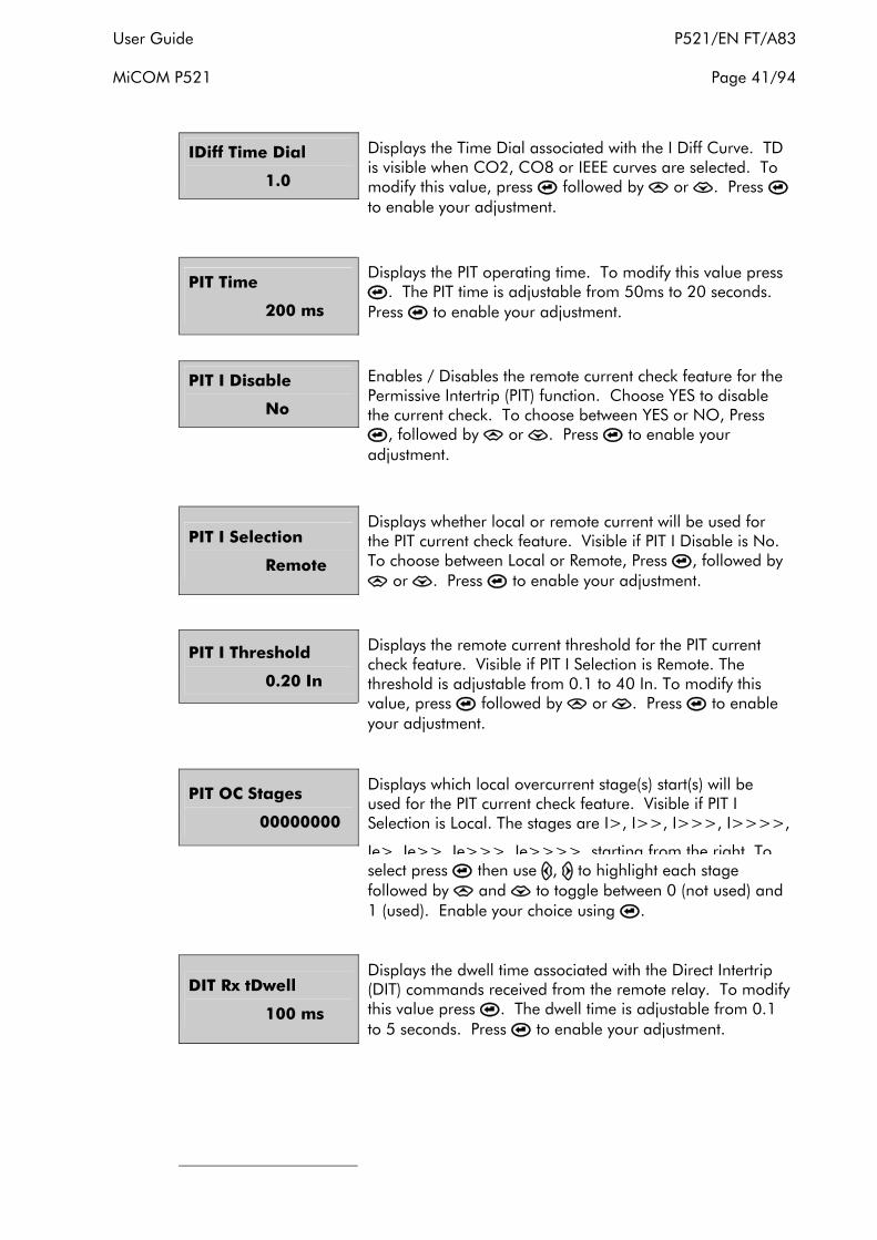
User Guide P521/EN FT/A83 MiCOM P521 Page 41/94
IDiff Time Dial
1.0
Displays the Time Dial associated with the I Diff Curve. TD is visible when CO2, CO8 or IEEE curves are selected. To modify this value, press followed by or . Press to enable your adjustment.
PIT Time
200 ms
Displays the PIT operating time. To modify this value press . The PIT time is adjustable from 50ms to 20 seconds.
Press to enable your adjustment.
PIT I Disable
No
Enables / Disables the remote current check feature for the Permissive Intertrip (PIT) function. Choose YES to disable the current check. To choose between YES or NO, Press
, followed by or . Press to enable your adjustment.
PIT I Selection
Remote
Displays whether local or remote current will be used for the PIT current check feature. Visible if PIT I Disable is No. To choose between Local or Remote, Press , followed by
or . Press to enable your adjustment.
PIT I Threshold
0.20 In
Displays the remote current threshold for the PIT current check feature. Visible if PIT I Selection is Remote. The threshold is adjustable from 0.1 to 40 In. To modify this value, press followed by or . Press to enable your adjustment.
PIT OC Stages
00000000
Displays which local overcurrent stage(s) start(s) will be used for the PIT current check feature. Visible if PIT I Selection is Local. The stages are I>, I>>, I>>>, I>>>>,
Ie>, Ie>>, Ie>>>, Ie>>>>, starting from the right To
select press then use , to highlight each stage followed by and to toggle between 0 (not used) and 1 (used). Enable your choice using .
DIT Rx tDwell
100 ms
Displays the dwell time associated with the Direct Intertrip (DIT) commands received from the remote relay. To modify this value press . The dwell time is adjustable from 0.1 to 5 seconds. Press to enable your adjustment.

P521/EN FT/A83 User Guide Page 42/94 MiCOM P521
DIT Alarm
Yes
Enables / Disables the Alarm LED illumination when a DIT signal is received. Choose YES to enable the illumination of yellow Alarm LED. To choose between YES or NO press , followed by or . Press to enable your adjustment.
PIT Alarm
Yes
Enables / Disables the Alarm LED illumination when a PIT signal is received. Choose YES to enable the illumination of yellow Alarm LED. To choose between YES or NO press , followed by or . Press to enable your adjustment.
CTS Is1
0.2 IN
Displays the Is1 threshold value for the situation when CT failure is detected and “Restraint” mode is chosen for differential. This Is1 threshold is adjustable from 0.2 to 4 In. To modify this value, press followed by or to select the desired value. Enable your choice using the key.
Inrush Option
Disabled
Display options for the inrush restraint/block facility. Choose from Disabled, Block and Restraint. To modify the setting, press , followed by or . Press to enable your adjustment.
High Set
4.0 IN
Displays the Idiff High Set setting when Inrush Option is enabled. To modify this value press . The High Set is adjustable from 4 to 32 In. Press to enable your adjustment.
Kr
4
Displays the Kr setting when Restraint mode is selected. The Kr is adjustable from 3 to 20. To modify this value press , followed by or . Press to enable your adjustment.
Harmonic Ratio
15%
Displays the I2/I1 setting when Block mode is selected. It is adjustable from 5% to 50%. To modify this value press , followed by or . Press to enable your adjustment.
Transient Bias
No
Enables/Disables the transient bias facility. Choose YES to enable transient bias facility. To choose between YES or NO press , followed by or . Press to enable

User Guide P521/EN FT/A83 MiCOM P521 Page 43/94
3.5.5.2 [50/51] Phase OC sub menu
PROTECTION G1 Heading of the PROTECTION G1 menu. To gain access to the [50/51] Phase OC sub menu, press , 4 times, then
and .
[50/51] Phase OC Heading of the [50/51] Phase OC sub menu. To gain access to the sub menu press .
I>?
Yes
Selection of the first phase threshold (I>). Select Yes, No or Backup. If the user enters I>(Yes or Backup), the following menu is displayed. If the user enters I> (No), go to I>> menu. If “Backup” is selected I> will only function in the event of a Protection Comms Failure.
I>
1 In
Displays the threshold current value I>. To modify this value, press . The threshold I> is adjustable from 0.1 to 25 In. Press to enable your adjustment.
I> Delay Type
DMT
Selection of the I> threshold time delay type. Select DMT for definite time, IDMT for inverse time curves or RI for the electromechanical inverse time curve.
3.5.5.2.1 I> DMT threshold menu
I> Delay Type
DMT
Displays the I> DMT time delay.
tI >
100 ms
Selection of the I> time delay. Select the time delay from 0 to 150 s using or and enable your choice using .
3.5.5.2.2 I> IDMT threshold, IEC or IEEE/ANSI curve menu
I> Delay Type
IDMT
Display the I> inverse time delay (IEC or IEEE/ANSI curves).
I> Curve
IEC SI
Selection of the I> curve. Select from IEC SI, IEC STI, IEC VI, IEC EI, IEC LTI, CO2, IEEE MI, CO8, IEEE VI, IEEE EI using or and enable your choice using the key .

P521/EN FT/A83 User Guide Page 44/94 MiCOM P521
I> Tms Displays the Time Multiplier Setting (TMS) associated with the IDMT Curve. TMS is visible when any of the IEC curves are selected. Select the curve TMS value. Select from
II> Time Dial
1.0
Displays the Time Dial associated with the IDMT Curve. Time Dial is visible when CO2, CO8 or IEEE curves are selected. Select from 0.1 to 100 using or and enable your choice using .
3.5.5.2.3 I> DMT reset time, IEEE/ANSI curves menu
Reset Type DMT
Selection of the type of reset time delay. Select between DMT (Definite Time) and IDMT (Inverse Time) using or
and enable your choice using .
tReset 40 ms Selection of the tReset value associated with the DMT reset time choice. Select from 40 ms to 100 s using or and enable your choice using .
3.5.5.2.4 I> IDMT reset time, IEEE/ANSI curves menu
Reset Type IDMT
Selection of the type of reset time delay. Select between DMT (Definitive Time) and IDMT (Inverse Time) using or
and enable your choice using .
Rtms 1.0 Selection of the Rtms value associated with the IDMT reset time choice. Select from 0.025 to 1.5 using or and enable your choice using .
3.5.5.2.5 I> IDMT threshold, electromechanical RI curve menu
I> Delay Type
RI
Display of the I> inverse time delay (electromechanical RI curve).
K
1.0
Selection of the RI curve K value. Select from 0.100 to 10 using or and enable your choice using .
3.5.5.2.6 I> DMT reset time, IEC / electromechanical RI curves menu
tReset
60 ms
Selection of the tReset value from 40 ms to 100 s using or and enable your choice using .
3.5.5.2.7 I>> threshold menu
I>>?
No
Selection of the I>> second phase threshold. Select Yes, No or Backup. If the user enters I>>(Yes or Backup), the following menu is displayed. If the user enters I>> (No) go

User Guide P521/EN FT/A83 MiCOM P521 Page 45/94
I>>
10 In
Selection of the I>> second threshold current value. To modify this value, press . The threshold I>> is adjustable from 0.5 to 40 In using or . Press to enable your adjustment.
I>> Delay Type
DMT
Selection of the I>> time delay type threshold. Select DMT for definite time, IDMT for inverse time curves, RI for electromechanical inverse time curve. According to this setting, additional settings appear, as shown for I> above.
tI >>
100 ms
Selection of the second threshold I>> time delay. Select the time delay from 0 to 150 s using or and enable your choice using .
3.5.5.2.8 I>>> threshold menu
I>>>?
No
Selection of the I>>> third phase threshold. Select Yes, No or Backup. If the user enters I>>>(Yes or Backup), the following menu is displayed. If the user enters I>>> (No) go to I>>>> menu.
If “Backup” is selected I>>> will only function in the event of a Protection Comms Failure.
I>>>
10 In
Selection of the I>>> third threshold current value. To modify this value, press . The threshold I>>> is adjustable from 0.5 to 40 In. Press to enable your adjustment.
tI >>>
100 ms
Selection of the third threshold I>>> time delay. Select the time delay from 0 to 150 s using or and enable your choice using .

P521/EN FT/A83 User Guide Page 46/94 MiCOM P521
3.5.5.2.9 I>>>> threshold menu
I>>>>?
No
Selection of the I>>>> fourth phase threshold. Select Yes, No or Backup. If the user enters I>>>> (Yes or Backup), the following menu is displayed. If the user enters I>>>> (No), the LCD display returns to the heading of the menu [50/51] Phase OC.
If “Backup” is selected I>>>> will only function in the event of a Protection Comms Failure.
I>>>>
10 In
Selection of the I>>>> fourth threshold current value. To modify this value, press . The threshold I>>>> is adjustable from 0.5 to 40 In. Press to enable your adjustment.
tI >>>>
100 ms
Selection of the fourth threshold I>>>> time delay. Select the time delay from 0 to 150 s using or and enable your choice using .
3.5.5.3 [50N/51N] Earth OC sub menu
PROTECTION G1 Heading of the PROTECTION G1 menu. To gain access to the [50N/51N] E/Gnd sub menu, press , 4 times, and twice.
[50N/51N] E/Gnd Heading of the [50N/51N] E/Gnd sub menu. To gain access to the sub menu content, press .
Ie>?
Yes
Selection of the first earth threshold (Ie>). Select Yes, No or Backup. If the user enters Ie>(Yes or Backup), the following menu is displayed. If the user enters > (No), go to Ie>> menu.
If “Backup” is selected Ie> will only function in the event of a Protection Comms Failure.
le >
0.05 Ien
Displays the current threshold value Ie>. To modify this value, press . The threshold Ie> is adjustable from: 0.002 to 1 Ien (0.002 to 1 Ien Range), 0.01 to Ien (0.01 to 8 Ien Range) and 0.1 to 25 Ien (0.1 to 40 Ien Range). Press
to enable your adjustment.
Ie> Delay Type
DMT
Selection of the Ie> threshold time delay type. Select from DMT for definite time, IDMT for inverse time curves, RI for the electromechanical inverse time curve or LABOR. for

User Guide P521/EN FT/A83 MiCOM P521 Page 47/94
3.5.5.3.1 Ie> DMT threshold menu
Ie> Delay Type
DMT
Displays the Ie> DMT time delay.
tIe >
100 ms
Selection of the Ie> time delay. Select the time delay from 0 to 150 s using or and enable your choice using .
3.5.5.3.2 Ie> IDMT threshold, IEC or IEEE/ANSI curves menu
Ie> Delay Type
IDMT
Displays the Ie> inverse time delay (IEC or IEEE/ANSI curves).
Ie> Curve
IEC SI
Selection of the Ie> curve. Select from IEC SI, IEC STI, IEC VI, IEC EI, IEC LTI, CO2, IEEE MI, CO8, IEEE VI, IEEE EI using or and enable your choice using the key .
Ie> Tms
1.0
Displays the Time Multiplier Setting (TMS) associated with the IDMT Curve. TMS is visible when any of the IEC curves are selected. Select the curve TMS value. Select from 0.025 to 1.5 using or and enable your choice using .
Ie> Time Dial
1.0
Displays the Time Dial associated with the IDMT Curve. Time Dial is visible when CO2, CO8 or IEEE curves are selected. Select from 0.1 to 100 using or and enable your choice using .
3.5.5.3.3 Ie> DMT reset time, IEEE/ANSI curves menu
Reset Type DMT
Selection of the type of reset time delay. Select between DMT (Definitive Time) and IDMT (Inverse Time) using or
and enable your choice using .
TReset
40 ms
Selection of the tReset value associated with the DMT reset time choice. Select from 40 ms to 100 s using or and enable your choice using .
3.5.5.3.4 Ie> IDMT reset time, ANSI curves menu
Reset Type IDMT
Selection of the type of reset time delay. Select between DMT (Definitive Time) and IDMT (Inverse Time) using or
and enable your choice using .

P521/EN FT/A83 User Guide Page 48/94 MiCOM P521
Rtms 1.0 Selection of the Rtms value associated with the IDMT reset time choice. Select from 0.025 to 1.5 using or and enable your choice using .
3.5.5.3.5 Ie> IDMT threshold, electromechanical RI curve menu
Ie> Delay type
RI
Displays the Ie> inverse time delay (electromechanical RI curve).
K
1.0
Selection of the RI curve K value. Select from 0.100 to 10 using or and enable your choice using .
3.5.5.3.6 Ie> DMT reset time, IEC/RI curves menu
tReset
60 ms
Selection of the tReset value from 40 ms to 100 s using or and enable your choice using .
3.5.5.3.7 Ie> IDMT threshold, Laborelec curve menu
Ie> Delay type
LABOR.
Displays the Ie> inverse time delay (Laborelec curve).
Ie> Curve
1
Selection of the Laborelec curve. Select from Curve 1, 2 or 3 using or and enable your choice using .
tReset
40 ms
Selection of the tReset value from 40 ms to 100 s using or and enable your choice using .
3.5.5.3.8 Ie>> threshold menu
Ie>>?
No
Selection of the Ie>> second earth threshold. Select Yes, No or Backup. If the user enters Ie>>(Yes or Backup), the following menu is displayed. If the user enters Ie>> (No) go to Ie>>> menu.
If “Backup” is selected Ie>> will only function in the event of a Protection Comms Failure.
Ie>> 5 Ien Selection of the Ie>> second threshold current value. To modify this value, press . The threshold Ie>> is adjustable from : 0.002 to 1Ien (0.002 to 1 Ien Range)
Ie>> Delay Type
DMT
Selection of the Ie>> threshold time delay type. Select DMT for definite time, IDMT for inverse time curves, RI for electromechanical inverse time curve. According to this

User Guide P521/EN FT/A83 MiCOM P521 Page 49/94
tIe>>
100 ms
Selection of the second threshold Ie>> time delay. Select the time delay from 0 to 150 s using or and validate your choice using .
3.5.5.3.9 Ie>>> threshold menu
Ie>>>?
No
Selection of the Ie>>> third earth threshold. Select Yes, No or Backup. If the user enters Ie>>> (Yes or Backup), the following menu is displayed. If the user enters Ie>>> (No) go to Ie>>> menu.
If “Backup” is selected Ie>>> will only function in the event of a Protection Comms Failure.
Ie>>>
10 Ien
Selection of the Ie>>> third threshold current value. To modify this value, press . The threshold Ie>>> is adjustable from 0.5 to 40 Ien. Press to validate your adjustment.
tIe>>>
100 ms
Selection of the third threshold Ie>>> time delay. Select the time delay from 0 to 150 s using or and validate your choice using .
3.5.5.3.10 Ie>>>> threshold menu
Ie>>>>?
Yes
Selection of the Ie>>>> fourth earth threshold. Select Yes, No or Backup. If the user validates Ie>>>(Yes), the following menu is displayed. If the user enters Ie>>> (No), the LCD display returns to the heading of the menu [50N/51N] E/Gnd.
If “Backup” is selected Ie>>>> will only function in the event of a Protection Comms Failure.
Ie>>>>
10 Ien
Selection of the Ie>>>> fourth threshold current value. To modify this value, press . The threshold Ie>>>> is adjustable from 0.5 to 40 Ien. Press to validate your adjustment.
tIe>>>>
100 ms
Selection of the third threshold Ie>>>> time delay. Select the time delay from 0 to 150 s using or and validate your choice using .

P521/EN FT/A83 User Guide Page 50/94 MiCOM P521
3.5.5.4 [46] Negative phase sequence I2> sub menu
PROTECTION G1 Heading of the PROTECTION G1 menu. To gain access to the [46] Neg Seq OC sub menu, press , 4 times, then
and 3 times.
[46] Neg Seq OC Heading of the [46] NEGATIVE Phase SEQUENCE I2>sub menu. To gain access to the sub menu content, press .
I2>?
No
Selection of the negative phase sequence overcurrent function. Select Yes or No. If the user validates (Yes), the following menu is displayed. If the user selects (No), the menu is deactivated.
I2>
0.1 In
Displays the negative sequence current threshold value I2>. To modify this value, press . The threshold I2> is adjustable from 0.1 to 40 In, in steps of 0.01 In. Press to validate your adjustment.
I2> Delay Type
DMT
Selection of the I2> threshold time delay type. Select from DMT for definite time, IDMT for inverse time curves or RI for the electromechanical inverse time curve. To make a selection use or and validate your choice using .
3.5.5.4.1 I2> DMT threshold menu
I2> Delay Type
DMT
Displays the I2> DMT time delay.
t I2 >
100 ms
Selection of the I2> time delay. Select the time delay from 0 to 150 s using or and validate your choice using .
3.5.5.4.2 I2> IDMT threshold, IEC or IEEE/ANSI curves menu
I2> Delay Type
IDMT
Displays the I2> inverse time delay (IEC or IEEE/ANSI curves).
I2> Curve
IEC SI
Selection of the I2> curve. Select from IEC SI, IEC STI, IEC VI, IEC EI, IEC LTI, CO2, IEEE MI, CO8, IEEE VI, IEEE EI using or and validate your choice using the key .

User Guide P521/EN FT/A83 MiCOM P521 Page 51/94
I2> Tms
0,025
Displays the Time Multiplier Setting (TMS) associated with the IDMT Curve. TMS is visible when any of the IEC curves are selected. Select from 0.025 to 1.5 using or and validate your choice using .
I2> Time Dial
1.0
Displays the Time Dial associated with the IDMT Curve. Time Dial is visible when CO2, CO8 or IEEE curves are selected. Select from 0.1 to 100 using or and enable your choice using .
3.5.5.4.2.1 I2> DMT reset time, IEC curves menu
tReset
60 ms
Selection of the tReset value from 40 ms to 100 s using or and validate your choice using .
3.5.5.4.2.2 I2> DMT reset time, IEEE/ANSI curves menu
Reset Type DMT
Selection of the type of reset time delay. Select between DMT (Definitive Time) and IDMT (Inverse Time) using or
and validate your choice using .
tReset
40 ms
Selection of the tReset value associated with the DMT reset time choice. Select from 40 ms to 100 s using or and validate your choice using .
3.5.5.4.2.3 I2> IDMT reset time, IEEE/ANSI curves menu
Reset Type IDMT
Selection of the type of reset time delay. Select between DMT (Definitive Time) and IDMT (Inverse Time) using or
and validate your choice using .
Rtms
0.025
Selection of the Rtms value associated with the IDMT reset time choice. Select from 0.025 to 1.5 using or and validate your choice using .
3.5.5.4.3 I2> IDMT threshold, electromechanical RI curve menu
I2> Delay Type
RI
Display of the I2> inverse time delay (electromechanical RI curve).
K
2.500
Selection of the RI curve K value. Select from 0.100 to 10 using or and validate your choice using .

P521/EN FT/A83 User Guide Page 52/94 MiCOM P521
3.5.5.4.3.1 I2> DMT reset time, RI curves
t Reset
60 ms
Selection of the t Reset value from 40 ms to 100 s using or and validate your choice using .
3.5.5.4.4 I2>> threshold menu
I2>>?
Yes
Selection of the 2nd threshold of the negative phase sequence overcurrent function. Select Yes or No. If the user validates (Yes), the following menu is displayed. If the user selects (No), the menu is deactivated.
I2>>
1 In
Displays the value of the 2nd threshold of the negative phase sequence overcurrent function. To modify this value, press . The threshold I2>> is adjustable from 0.1 In to 40 In, in steps of 0.01 In. Press to validate your adjustment.
tI2>>
150 ms
Selection of the 2nd threshold I2>> time delay. Select the time delay from 0 to 150 s using or and validate your choice using .
3.5.5.5 [49] Therm OL sub menu
PROTECTION G1 Heading of the PROTECTION G1 menu. To gain access to the [49] Thermal OL sub menu, press , 4 times, then
and 4 times.
[49] Therm OL Heading of the Thermal OL menu. To gain access to the sub menu content press .
Therm OL?
Yes
Selection of the thermal overload function. Select Yes or No. If the user enters Yes, the following menu is displayed. If the user enters No, the menu is deactivated.
Iθ >
0.5 In
Displays the thermal current threshold value Iθ>. To modify this value, press . The threshold Iθ> is adjustable from 0.1 to 3.2 In, in steps of 0.01.
Press to validate your choice.
Te
10 mn
Displays the thermal time constant (Te) associated with the thermal overload formula. To modify this value, press . The time constant Te is adjustable from 1 to 200 minutes, in steps of 1 min.

User Guide P521/EN FT/A83 MiCOM P521 Page 53/94
K
1.05
Displays the k factor associated with the thermal overload function. To modify this value, press . The k factor is adjustable from 1 to 1.5, in steps of 0.01.
Press to validate your adjustment.
θ Trip
110 %
Displays the percentage applicable to the thermal overload trip threshold. To modify this value, press . θ Trip is adjustable from 50 % to 200 % in steps of 1%.
Press to validate your adjustment.
θ Alarm?
Yes
Selection of the thermal overload alarm function. Select Yes or No. If the user validates (Yes), the following menu is displayed. If the user selects (No), the thermal overload alarm will be disabled.
θ Alarm
90 %
Displays the percentage applicable to the thermal overload alarm threshold. To modify this value, press . θ Trip is adjustable from 50 % to 200 % step of 1%.
Press to validate your adjustment.
3.5.5.6 [37] Undercurrent I< sub menu
[37] Under Current
Heading of the [37] Under-Current sub menu. To gain access to the sub menu content, press .
I<?
Yes
Selection of the undercurrent function. Select Yes or No. If the user validates (Yes), the following menu is displayed. If the user selects (no) the menu is deactivated.
I<
0.2 In
Displays the undercurrent threshold value I<. To modify this value, press . The threshold I< is adjustable from 0.02 In to 1 In, in steps of 0.01 In. Press to validate
tI<
200 ms
Selection of the time delay associated with the undercurrent threshold. Select the time delay from 0 s to 150 s using or and validate your choice using .

P521/EN FT/A83 User Guide Page 54/94 MiCOM P521
3.5.6 Automat. ctrl menu
The AUTOMAT. CTRL Menu makes it possible to programme the various automation functions included in the MiCOM P521.
The various sub menus are:
⇒ Commissioning
⇒ Trip Commands
⇒ Latch Functions (latch of the trip output relay RL1)
⇒ Blocking Logic 1
⇒ Blocking Logic 2
⇒ Logic Select. 1
⇒ Logic Select. 2
⇒ Outputs Relays
⇒ Latch Output Relays (latch of the auxiliary output relays)
⇒ Invert Output Relays
⇒ Inputs
⇒ Broken Conductor
⇒ Cold Load PU
⇒ CB Fail
⇒ CB Supervision
⇒ Logic Equations
⇒ Program. I-Trip (inter-trips)
⇒ CT Supervision
To access the AUTOMAT. CTRL Menu, press followed by six times.
3.5.6.1 Commissioning sub menu
This sub menu has been designed as a commissioning tool to aid testing. It makes it possible to disable output contacts and freeze circuit breaker measurements (such as number of operation etc.). In addition, this menu allows the user to perform a contact and LED test. A “Loopback” facility is also provided so that the relay can be fully tested in the absence of a remote relay (see also section 4.2.6 of the Commissioning and Maintenance chapter (P521/EN CM) for more information).
AUTOMAT.CTRL Heading of the AUTOMAT. CTRL Menu. To gain access to the commissioning menu, press , 6 times then .
Commissioning Heading of the Commissioning sub menu. To gain access to the sub menu points, press .

User Guide P521/EN FT/A83 MiCOM P521 Page 55/94
Commissioning?
No
Enables / Disables of the Commissioning facilities. Select Yes or No.
If the user validates (Yes), the following menu is displayed. If the user selects (No) the menu is deactivated.
LED Test
No
Allows the user to illuminate all eight LED’s on the front of the P521. To illuminate the LED’s select (Yes) and Press . The LED’s will remain illuminated for 5 seconds after the key is pressed. If (No) is selected the relay will not perform an LED test.
Disable Relays
No
Enables / Disables all outputs contacts. To disable the output contacts select (Yes). The TRIP LED and LCD will continue to function correctly even with the contacts disabled. An “ISOLATED RELAYS” ALARM (accompanied by the alarm LED) will be generated when the contacts are disabled. The alarm can only be reset when output contacts are re-enabled by selecting (No).
Trip 87654321 Test: 00000000
Allocation of contacts to be tested.
To allocate the trip test to the output relay(s), press , then select the desired output relay with the value 1 using . Repeat the operation on the other output relays if desired, then validate using .
Contact Test
No
Allows the user to operate the selected contacts. To operate the selected contacts press followed by to select (Yes). The contacts will remain operated whilst (Yes) is selected. To deactivate the contacts select (No).
Disable CB Stats:
No
Allows the user to “freeze” the Circuit breaker measurements in the RECORDS/CB Monitoring menu. To freeze the measurements press followed by to select (Yes). To re-activate the CB measurements, select (No) and validate your choice using .
Loopback Test
OFF
Allows the user to set the Loopback Test to CHANNEL_1 or INTERNAL. In these modes the relay will only accept messages from itself and no other relay. When choosing CHANNEL_1, to avoid a COMMS FAIL alarm the transmit (Tx) and receive (Rx) must be connected together on the protection comms channel. While in INTERNAL mode, it is not necessary to connect Tx and Rx. To enable the Loopback Test press followed by to select (CHANNEL_1 or INTERNAL). This will be accompanied by the LOOPBACK MODE alarm. To deactivate the Loopback Test, select (OFF).

P521/EN FT/A83 User Guide Page 56/94 MiCOM P521
I Diff Trip Flags
TRIP: A, B, C
Indicates which phase (A, B or C) is currently operating due to the current differential protection. Indication is given as soon as the current enters the “trip region” but will reset once the current exits this region.
3.5.6.2 Trip commands sub menu
This sub menu makes it possible to assign selected thresholds to the trip output (RL1).
AUTOMAT. CTRL Heading of the AUTOMAT. CTRL Menu. To gain access to the Trip Commands menu, press , 6 times, , then .
Trip Commands Heading of the Trip ORDER sub menu. To gain access to the sub menu points, press .
Trip Idiff
Yes
Allocates the current differential protection to the trip output (select Yes or No). If the user validates Yes, the trip output relay (RL1) will be activated when the current differential
Trip Direct
I-Trip Yes
Allocates the Direct Intertrip function to the trip output. Select Yes or No.
Trip C Diff
I-Trip Yes
Allocates the Current Differential Intertrip function to the trip output relay. Select Yes or No.
Trip PIT
Yes
Allocates the Permissive Intertrip function to the trip output relay. Select Yes or No.
Trip tI>
Yes
Allocates the first phase time delay overcurrent threshold (tI>) to the trip output (select Yes or No). If the user validates Yes, the trip output relay (RL1) will be activated at the end of the time delay tI>. If the user validates No, the trip output relay (RL1) will never be activated, even at the end of the time delay tI>.
Trip tI>>
Yes
Allocates the second phase time delay overcurrent threshold (tI>>) to the trip output. Select Yes or No.

User Guide P521/EN FT/A83 MiCOM P521 Page 57/94
Trip tI>>>
Yes
Allocates the third phase time delay overcurrent threshold (tI>>>) to the trip output. Select Yes or No.
Trip tI>>>>
Yes
Allocates the fourth phase time delay overcurrent threshold (tI>>>>) to the trip output. Select Yes or No.
Trip tIe>
Yes
Allocates the first earth fault time delay threshold (tIe>) to the trip output. Select Yes or No.
Trip tIe>>
Yes
Allocates the second earth fault time delay threshold (tIe>>) to the trip output. Select Yes or No.
Trip tIe>>>
Yes
Allocates the third earth fault time delay threshold (tIe>>>) to the trip output. Select Yes or No.
Trip tIe>>>>
Yes
Allocates the fourth earth fault time delay threshold (tIe>>>>) to the trip output. Select Yes or No.
Trip tI<
Yes
Allocates of the under current threshold (tI<) to the trip output. Select Yes or No.
Trip tI2>
Yes
Allocates the first time delayed negative phase sequence overcurrent threshold (tI2>) to the trip output. Select Yes or No.
Trip tI2>>
Yes
Allocates the second time delayed negative phase sequence overcurrent threshold (tI2>>) to the trip output. Select Yes or No.
Trip Thermal θ
Yes
Allocates the thermal overload Trip (θTrip) to the trip output. Select Yes or No.
Trip Brkn.Cond
Yes
Allocates the broken conductor detection to the trip output. Select Yes or No.

P521/EN FT/A83 User Guide Page 58/94 MiCOM P521
Trip tAux 1
Yes
Allocates the auxiliary timer Aux 1 to the trip output. Select Yes or No.
Trip tAux 2
Yes
Allocates the auxiliary timer Aux 2 to the trip output. Select Yes or No.
TCS Block
No
Allocates the TCS Block signal to the trip output. Select Yes or No.
Trip Equ A
No
Allocates the Logic Equation A operate signal to the trip output. Select Yes or No.
Trip Equ B
No
Allocates the Logic Equation B operate signal to the trip output. Select Yes or No.
Trip Equ C
No
Allocates the Logic Equation C operate signal to the trip output. Select Yes or No.
Trip Equ D
No
Allocates the Logic Equation D operate signal to the trip output. Select Yes or No.
Trip Equ E
No
Allocates the Logic Equation E operate signal to the trip output. Select Yes or No.
Trip Equ F
No
Allocates the Logic Equation F operate signal to the trip output. Select Yes or No.
Trip Equ G
No
Allocates the Logic Equation G operate signal to the trip output. Select Yes or No.

User Guide P521/EN FT/A83 MiCOM P521 Page 59/94
Trip Equ H
No
Allocates the Logic Equation H operate signal to the trip output. Select Yes or No.
3.5.6.3 Latch functions sub menu
This sub menu makes it possible to latch the trip output relay RL1 after being operated by one or several thresholds.
AUTOMAT. CTRL Heading of the AUTOMAT. CTRL Menu. To gain access to the Latch Functions menu, press , , 6 times, , then twice.
Latch Functions Heading of the Latch Functions sub menu. To gain access to the sub menu points, press .
Latch Idiff
No
Latches the trip output relay RL1 once the current differential protection (Idiff) has operated (select Yes or No). If the user validates Yes, RL1 will be latched even after Idiff has reset. If the user validates No, RL1 will “drop off” after Idiff has reset.
Latch Direct
I-Trip No
Latch the trip output RL1 once the Direct Intertrip function has operated.
Latch C Diff
I-Trip No
Latch the trip output RL1 once the Current Differential Intertrip function has operated.
Latch PIT
No
Latch the trip output RL1 once the Permissive Intertrip function has operated.
Latch tI>
No
Latches the trip output relay RL1 once the first time delayed phase overcurrent threshold (tI>) has operated. Select Yes or No.
Latch tI>>
No
Latches the trip output relay RL1 once the second time delayed phase overcurrent threshold (tI>>) has operated. Select Yes or No.
Latch tI>>>
No
Latches the trip output relay RL1 once the third time delayed phase overcurrent threshold (tI>>>) has operated. Select Yes or No.

P521/EN FT/A83 User Guide Page 60/94 MiCOM P521
Latch tI>>>>
No
Latches the trip output relay RL1 once the fourth time delayed phase overcurrent threshold (tI>>>>) has operated. Select Yes or No.
Latch tIe>
No
Latches the trip output relay RL1 once the first time delayed earth fault threshold (tIe>) has operated. Select Yes or No.
Latch tIe>>
No
Latches the trip output relay RL1 once the second time delayed earth fault threshold (tIe>>) has operated. Select Yes or No.
Latch tIe>>>
No
Latches the trip output relay RL1 once the third time delayed earth fault threshold (tIe>>>) has operated. Select Yes or No.
Latch tIe>>>>
No
Latches the trip output relay RL1 once the fourth time delayed earth fault threshold (tIe>>>>) has operated. Select Yes or No.
Latch tI<
No
Latches the trip output relay RL1 once the time delayed under current threshold (tI<) has operated. Select Yes or No.
Latch tI2>
No
Latches the trip output relay RL1 once the first time delayed negative sequence over current threshold (tI2>) has operated. Select Yes or No.
Latch tI2>>
No
Latches the trip output relay RL1 once the second time delayed negative sequence over current threshold (tI2>>) has operated. Select Yes or No.
Latch Thermal θ
No
Latches the trip output relay RL1 once the thermal element has operated. Select Yes or No.
Latch Brkn.Cond
No
Latches the trip output relay RL1 once the broken conductor protection has operated. Select Yes or No.
Latch t Aux 1
No
Latches the trip output relay RL1 once auxiliary timer 1 has operated. Select Yes or No.

User Guide P521/EN FT/A83 MiCOM P521 Page 61/94
Latch t Aux 2
No
Latches the trip output relay RL1 once auxiliary timer 2 has operated. Select Yes or No.
Latch TCS Block
No
Latches the trip output relay RL1 once TCS Block has operated. Select Yes or No.
Latch Equ A
No
Latches the trip output relay RL1 once Logic Equation A has operated. Select Yes or No.
Latch Equ B
No
Latches the trip output relay RL1 once Logic Equation B has operated. Select Yes or No.
Latch Equ C
No
Latches the trip output relay RL1 once Logic Equation C has operated. Select Yes or No.
Latch Equ D
No
Latches the trip output relay RL1 once Logic Equation D has operated. Select Yes or No.
Latch Equ E
No
Latches the trip output relay RL1 once Logic Equation E has operated. Select Yes or No.
Latch Equ F
No
Latches the trip output relay RL1 once Logic Equation F has operated. Select Yes or No.
Latch Equ G
No
Latches the trip output relay RL1 once Logic Equation G has operated. Select Yes or No.
Latch Equ H
No
Latches the trip output relay RL1 once Logic Equation H has operated. Select Yes or No.
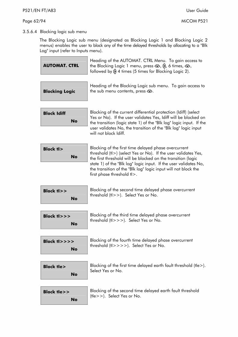
P521/EN FT/A83 User Guide Page 62/94 MiCOM P521
3.5.6.4 Blocking logic sub menu
The Blocking Logic sub menu (designated as Blocking Logic 1 and Blocking Logic 2 menus) enables the user to block any of the time delayed thresholds by allocating to a "Blk Log" input (refer to Inputs menu).
AUTOMAT. CTRL Heading of the AUTOMAT. CTRL Menu. To gain access to the Blocking Logic 1 menu, press , , 6 times, , followed by 4 times (5 times for Blocking Logic 2).
Blocking Logic Heading of the Blocking Logic sub menu. To gain access to the sub menu contents, press .
Block Idiff
No
Blocking of the current differential protection (Idiff) (select Yes or No). If the user validates Yes, Idiff will be blocked on the transition (logic state 1) of the "Blk log" logic input. If the user validates No, the transition of the "Blk log" logic input will not block Idiff.
Block tI>
No
Blocking of the first time delayed phase overcurrent threshold (tI>) (select Yes or No). If the user validates Yes, the first threshold will be blocked on the transition (logic state 1) of the "Blk log" logic input. If the user validates No, the transition of the "Blk log" logic input will not block the first phase threshold tI>.
Block tI>>
No
Blocking of the second time delayed phase overcurrent threshold (tI>>). Select Yes or No.
Block tI>>>
No
Blocking of the third time delayed phase overcurrent threshold (tI>>>). Select Yes or No.
Block tI>>>>
No
Blocking of the fourth time delayed phase overcurrent threshold (tI>>>>). Select Yes or No.
Block tIe>
No
Blocking of the first time delayed earth fault threshold (tIe>). Select Yes or No.
Block tIe>>
No
Blocking of the second time delayed earth fault threshold (tIe>>). Select Yes or No.

User Guide P521/EN FT/A83 MiCOM P521 Page 63/94
Block tIe>>>
No
Blocking of the third time delayed earth fault threshold (tIe>>>). Select Yes or No.
Block tIe>>>>
No
Blocking of the fourth time delayed earth fault threshold (tIe>>>>). Select Yes or No.
Block tI2 >
No
Blocking of the first time delayed negative phase sequence overcurrent threshold (tI2>). Select Yes or No.
Block tI2 >>
No
Blocking of the second time delayed negative phase sequence overcurrent threshold (tI2>>). Select Yes or No.
Block Thermal θ
No
Blocking of the thermal protection. Select Yes or No.
Block Brkn.Cond
No
Blocking of the broken conductor protection. Select Yes or No.
Block t Aux 1
No
Blocking of the auxiliary timer 1 (tAux1). Select Yes or No.
Block t Aux 2
No
Blocking of the auxiliary timer 2 (tAux2). Select Yes or No.
Block Equation
A No
Blocking of the Logic Equation A. Select Yes or No.
Block Equation
B No
Blocking of the Logic Equation B. Select Yes or No.
Block Equation
C No
Blocking of the Logic Equation C. Select Yes or No.

P521/EN FT/A83 User Guide Page 64/94 MiCOM P521
Block Equation
D No
Blocking of the Logic Equation D. Select Yes or No.
Block Equation
E No
Blocking of the Logic Equation E. Select Yes or No.
Block Equation
F No
Blocking of the Logic Equation F. Select Yes or No.
Block Equation
G No
Blocking of the Logic Equation G. Select Yes or No.
Block Equation
H No
Blocking of the Logic Equation H. Select Yes or No.
3.5.6.5 Logic select sub menus
The Logic Select sub menus (designated as Logic Select. 1 and Logic Select. 2) sub menus enable the user to allocate a time delay threshold to the "Log sel" input (refer to Inputs menu). When the "Log sel" input is energized the selected overcurrent and earth fault time delays will change to the tSEL1 or tSEL2 time.
AUTOMAT. CTRL Heading of the AUTOMAT. CTRL Menu. To gain access to the Logic Select. 1 menu, press , , 6 times, , followed by 6 times (7 times for Logic Select. 2).
Logic Select. 1 Heading of the Logic Select. 1 sub menu. To gain access to the sub menu contents, press .
Sel1 tI>>
No
Logic selectivity of the second time delayed phase overcurrent threshold (tI>>) (select Yes or No). If the user validates Yes, operation of the second threshold will be delayed for tSel1 on the transition (logic state 1) of the "Log Sel 1" logic input. If the user validates No, the transition of the "Log Sel 1" logic input will not alter the second threshold tI>>.
Sel1 tI>>>
No
Logic selectivity of the third time delayed phase overcurrent threshold (tI>>>). Select Yes or No.

User Guide P521/EN FT/A83 MiCOM P521 Page 65/94
Sel1 tI>>>>
No
Logic selectivity of the fourth time delayed phase overcurrent threshold (tI>>>). Select Yes or No.
Sel1 tIe>>
No
Logic selectivity of the second time delayed earth fault threshold (tIe>>). Select Yes or No.
Sel1 tIe>>>
No
Logic selectivity of the third time delayed earth fault threshold (tIe>>>). Select Yes or No.
Sel1 tIe>>>>
No
Logic selectivity of the fourth time delayed earth fault threshold (tIe>>>>). Select Yes or No.
tSel1
0 ms
Displays the selective scheme logic time delay t Sel1. To modify this value, press . The tSel1 is adjustable from 0 ms to 150 s in steps of 10 ms. Press to validate your adjustment.
3.5.6.6 Output relays sub menu
This sub menu makes it possible to allocate an output relay (except Watchdog RL0) to the various thresholds (instantaneous and/or time delay). Note that the TRIP contact RL1 is allocated in the “Trip Commands” menu (under AUTOMAT. CTRL).
Output relay RL2 has change over contacts, whereas relays RL3 to RL8 have only normally open contacts.
AUTOMAT. CTRL Heading of the AUTOMAT. CTRL Menu. To gain access to the Output Relays menu, press , , 6 times, , followed by 8 times.
Output Relays Heading of the Output Relays sub menu. To gain access to the sub menu contents, press .
Trip 8765432
0000000
Allocates any trip order to the selected output relays (copies the trip contact onto one or several selected relays).
To select the desired output relay(s), press , then select the desired output relay with a value 1 using .Repeat the operation on the other output relays if desired, then validate using .
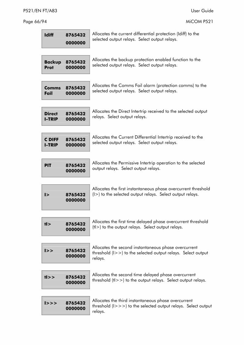
P521/EN FT/A83 User Guide Page 66/94 MiCOM P521
Idiff 8765432
0000000
Allocates the current differential protection (Idiff) to the selected output relays. Select output relays.
Backup 8765432 Prot 0000000
Allocates the backup protection enabled function to the selected output relays. Select output relays.
Comms 8765432 Fail 0000000
Allocates the Comms Fail alarm (protection comms) to the selected output relays. Select output relays.
Direct 8765432 I-TRIP 0000000
Allocates the Direct Intertrip received to the selected output relays. Select output relays.
C DIFF 8765432 I-TRIP 0000000
Allocates the Current Differential Intertrip received to the selected output relays. Select output relays.
PIT 8765432 0000000
Allocates the Permissive Intertrip operation to the selected output relays. Select output relays.
I> 8765432 0000000
Allocates the first instantaneous phase overcurrent threshold (I>) to the selected output relays. Select output relays.
tI> 8765432 0000000
Allocates the first time delayed phase overcurrent threshold (tI>) to the output relays. Select output relays.
I>> 8765432 0000000
Allocates the second instantaneous phase overcurrent threshold (I>>) to the selected output relays. Select output relays.
tI>> 8765432 0000000
Allocates the second time delayed phase overcurrent threshold (tI>>) to the output relays. Select output relays.
I>>> 8765432 0000000
Allocates the third instantaneous phase overcurrent threshold (I>>>) to the selected output relays. Select output relays.

User Guide P521/EN FT/A83 MiCOM P521 Page 67/94
tI>>> 8765432 0000000
Allocates the third time delayed phase overcurrent threshold (tI>>>) to the selected output relays. Select output relays.
I>>>> 8765432 0000000
Allocates the fourth instantaneous phase overcurrent threshold (I>>>) to the selected output relays. Select output relays.
tI>>>> 8765432 0000000
Allocates the fourth time delayed phase overcurrent threshold (tI>>>) to the selected output relays. Select output relays.
Ie> 8765432 0000000
Allocates the first instantaneous earth fault threshold (Ie>) to the selected output relays. Select output relays.
tIe> 8765432 0000000
Allocates the first time delayed earth fault threshold (tIe>) to the selected output relays. Select output relays.
Ie>> 8765432 0000000
Allocates the second instantaneous earth fault threshold (Ie>>) to the selected output relays. Select output relays.
tIe>> 8765432 0000000
Allocates the second time delayed earth fault threshold (tIe>>) to the selected output relays. Select output relays.
Ie>>> 8765432 0000000
Allocates the third instantaneous earth fault threshold (Ie>>>) to the selected output relays. Select output relays.
tIe>>> 8765432 0000000
Allocates the third time delayed earth fault threshold (tIe>>>) to the selected output relays. Select output relays.
Ie>>>> 8765432 0000000
Allocates the fourth instantaneous earth fault threshold (Ie>>>>) to the selected output relays. Select output relays.
tIe>>>> 8765432 0000000
Allocates the fourth time delayed earth fault threshold (tIe>>>>) to the selected output relays. Select output relays.
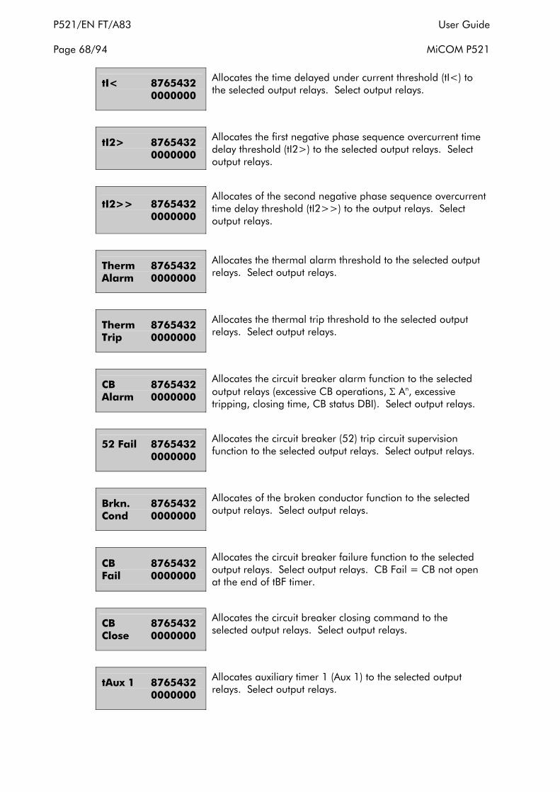
P521/EN FT/A83 User Guide Page 68/94 MiCOM P521
tI< 8765432 0000000
Allocates the time delayed under current threshold (tI<) to the selected output relays. Select output relays.
tI2> 8765432 0000000
Allocates the first negative phase sequence overcurrent time delay threshold (tI2>) to the selected output relays. Select output relays.
tI2>> 8765432 0000000
Allocates of the second negative phase sequence overcurrent time delay threshold (tI2>>) to the output relays. Select output relays.
Therm 8765432 Alarm 0000000
Allocates the thermal alarm threshold to the selected output relays. Select output relays.
Therm 8765432 Trip 0000000
Allocates the thermal trip threshold to the selected output relays. Select output relays.
CB 8765432 Alarm 0000000
Allocates the circuit breaker alarm function to the selected output relays (excessive CB operations, Σ An, excessive tripping, closing time, CB status DBI). Select output relays.
52 Fail 8765432 0000000
Allocates the circuit breaker (52) trip circuit supervision function to the selected output relays. Select output relays.
Brkn. 8765432 Cond 0000000
Allocates of the broken conductor function to the selected output relays. Select output relays.
CB 8765432 Fail 0000000
Allocates the circuit breaker failure function to the selected output relays. Select output relays. CB Fail = CB not open at the end of tBF timer.
CB 8765432 Close 0000000
Allocates the circuit breaker closing command to the selected output relays. Select output relays.
tAux 1 8765432 0000000
Allocates auxiliary timer 1 (Aux 1) to the selected output relays. Select output relays.

User Guide P521/EN FT/A83 MiCOM P521 Page 69/94
tAux 2 8765432 0000000
Allocates auxiliary timer 2 (Aux 2) to the selected output relays. Select output relays.
Active 8765432 Group 0000000
Allocates setting group 2 indication to the selected output relays. Select output relays.
TCS 8765432 Block 0000000
Allocates the TCS Block signal to the selected output relays. Select Yes or No.
Input1 8765432 0000000
Allocates the Input1 signal to the selected output relays. Select Yes or No.
Input2 8765432 0000000
Allocates the Input2 signal to the selected output relays. Select Yes or No.
Input3 8765432 0000000
Allocates the Input3 signal to the selected output relays. Select Yes or No.
Input4 8765432 0000000
Allocates the Input4 signal to the selected output relays. Select Yes or No.
Input5 8765432 0000000
Allocates the Input5 signal to the selected output relays. Select Yes or No.
Equ A 8765432 0000000
Allocates the Logic Equation A operate signal to the selected output relays. Select Yes or No.
Equ B 8765432 0000000
Allocates the Logic Equation B operate signal to the selected output relays. Select Yes or No.
Equ C 8765432 0000000
Allocates the Logic Equation C operate signal to the selected output relays. Select Yes or No.
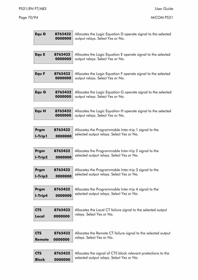
P521/EN FT/A83 User Guide Page 70/94 MiCOM P521
Equ D 8765432 0000000
Allocates the Logic Equation D operate signal to the selected output relays. Select Yes or No.
Equ E 8765432 0000000
Allocates the Logic Equation E operate signal to the selected output relays. Select Yes or No.
Equ F 8765432 0000000
Allocates the Logic Equation F operate signal to the selected output relays. Select Yes or No.
Equ G 8765432 0000000
Allocates the Logic Equation G operate signal to the selected output relays. Select Yes or No.
Equ H 8765432 0000000
Allocates the Logic Equation H operate signal to the selected output relays. Select Yes or No.
Prgm 8765432
I-Trip1 0000000
Allocates the Programmable Inter-trip 1 signal to the selected output relays. Select Yes or No.
Prgm 8765432
I-Trip2 0000000
Allocates the Programmable Inter-trip 2 signal to the selected output relays. Select Yes or No.
Prgm 8765432
I-Trip3 0000000
Allocates the Programmable Inter-trip 3 signal to the selected output relays. Select Yes or No.
Prgm 8765432
I-Trip4 0000000
Allocates the Programmable Inter-trip 4 signal to the selected output relays. Select Yes or No.
CTS 8765432
Local 0000000
Allocates the Local CT failure signal to the selected output relays. Select Yes or No.
CTS 8765432
Remote 0000000
Allocates the Remote CT failure signal to the selected output relays. Select Yes or No.
CTS 8765432
Block 0000000
Allocates the signal of CTS block relevant protections to the selected output relays. Select Yes or No.

User Guide P521/EN FT/A83 MiCOM P521 Page 71/94
CTS 8765432
Res. 0000000
Allocates the signal of CTS Restraint differential protections to the selected output relays. Select Yes or No.
Mode 8765432
Convent 0000000
Allocates the signal of protection communication frame in Convention mode to the selected output relays. Select Yes or No.
CDiff 8765432
Disable 0000000
Allocates the signal of current differential disabled to the selected output relays. Select Yes or No.
3.5.6.7 Latch of the auxiliary output relays
This sub menu makes it possible to latch the individual output relays. The latch can be reset by key once the function that initiated the relay has reset.
AUTOMAT. CTRL Heading of the AUTOMAT. CTRL Menu. To gain access to the Latch Output Relays menu, press , , 6 times, , followed by 9 times.
Latch Output Relays
Heading of the Latch Output Relays sub menu. To gain access to the sub menu content, press .
Output 2 No
Latch output relay RL2. Select Yes or No.
Output 3 No
Latch output relay RL3. Select Yes or No.
Output 4 No
Latch output relay RL4. Select Yes or No.
Output 5 No
Latch output relay RL5. Select Yes or No.
Output 6 No
Latch output relay RL6. Select Yes or No.

P521/EN FT/A83 User Guide Page 72/94 MiCOM P521
Output 7 No
Latch output relay RL7. Select Yes or No.
Output 8 No
Latch output relay RL8. Select Yes or No.
3.5.6.8 Inversion of the auxiliary output relays
This sub menu makes it possible to invert the state of the individual output relays while the relay is energized.
AUTOMAT. CTRL Heading of the AUTOMAT. CTRL Menu. To gain access to the Invert Output Relays menu, press , , 6 times, , followed by 10 times.
Invert Output Relays
Heading of the Invert Output Relays sub menu. To gain access to the sub menu content, press .
Output 2 No
Invert output relay RL2. Select Yes or No.
Output 3 No
Invert output relay RL3. Select Yes or No.
Output 4 No
Invert output relay RL4. Select Yes or No.
Output 5 No
Invert output relay RL5. Select Yes or No.
Output 6 No
Invert output relay RL6. Select Yes or No.
Output 7 No
Invert output relay RL7. Select Yes or No.
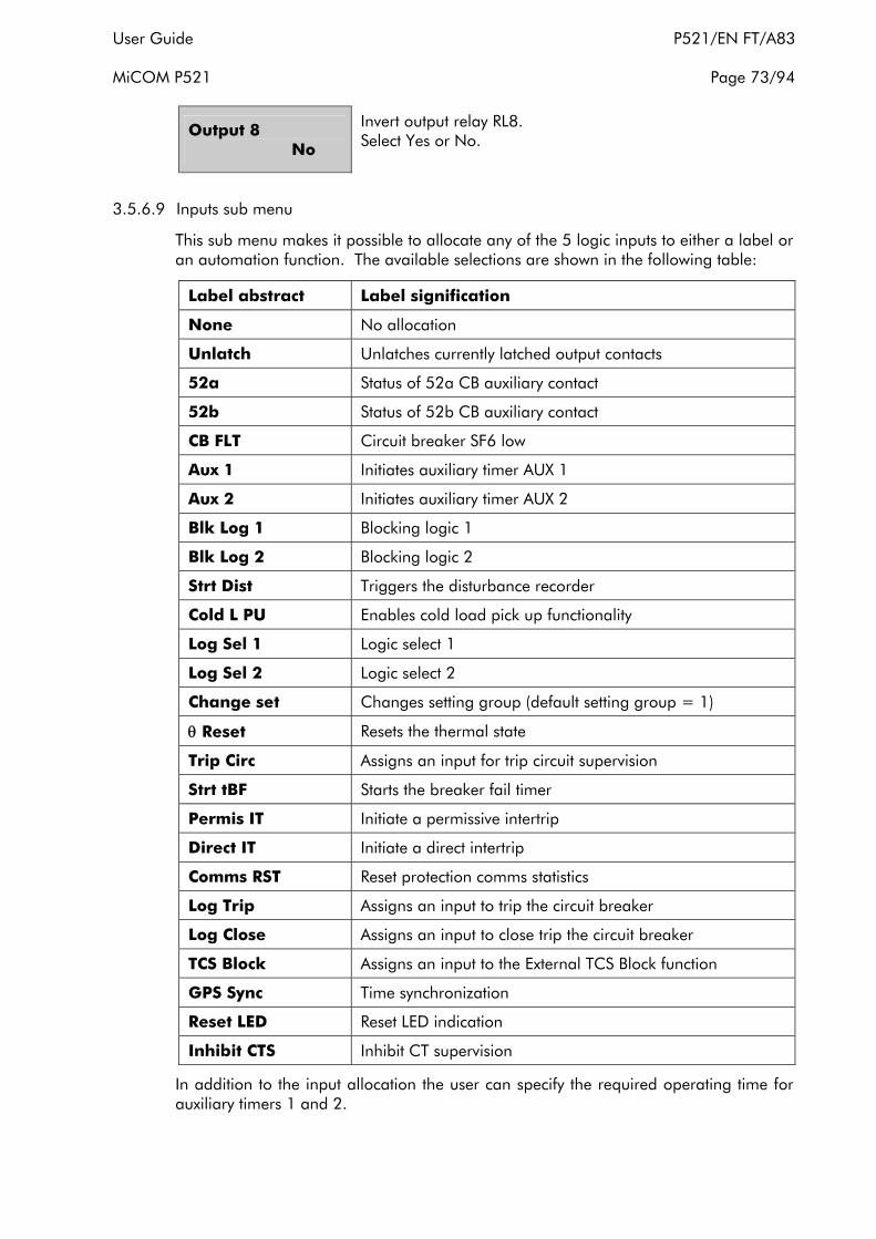
User Guide P521/EN FT/A83 MiCOM P521 Page 73/94
Output 8 No
Invert output relay RL8. Select Yes or No.
3.5.6.9 Inputs sub menu
This sub menu makes it possible to allocate any of the 5 logic inputs to either a label or an automation function. The available selections are shown in the following table:
Label abstract Label signification
None No allocation
Unlatch Unlatches currently latched output contacts
52a Status of 52a CB auxiliary contact
52b Status of 52b CB auxiliary contact
CB FLT Circuit breaker SF6 low
Aux 1 Initiates auxiliary timer AUX 1
Aux 2 Initiates auxiliary timer AUX 2
Blk Log 1 Blocking logic 1
Blk Log 2 Blocking logic 2
Strt Dist Triggers the disturbance recorder
Cold L PU Enables cold load pick up functionality
Log Sel 1 Logic select 1
Log Sel 2 Logic select 2
Change set Changes setting group (default setting group = 1)
θ Reset Resets the thermal state
Trip Circ Assigns an input for trip circuit supervision
Strt tBF Starts the breaker fail timer
Permis IT Initiate a permissive intertrip
Direct IT Initiate a direct intertrip
Comms RST Reset protection comms statistics
Log Trip Assigns an input to trip the circuit breaker
Log Close Assigns an input to close trip the circuit breaker
TCS Block Assigns an input to the External TCS Block function
GPS Sync Time synchronization
Reset LED Reset LED indication
Inhibit CTS Inhibit CT supervision
In addition to the input allocation the user can specify the required operating time for auxiliary timers 1 and 2.

P521/EN FT/A83 User Guide Page 74/94 MiCOM P521
AUTOMAT. CTRL Heading of the AUTOMAT. CTRL Menu. To gain access to the Inputs menu, press , , 6 times, , followed by 11 times.
Inputs Heading of the Inputs sub menu. To gain access to the sub menu content, press .
Input 1 None
Allocation of logic input 1. To allocate a function to logic input 1, press then use or to select the desired function from the available list. Validate your choice using .
Input 2 None
Allocation of logic input 2. To allocate a function to logic input 2, press then use or to select the desired function from the available list. Validate your choice using .
Input 3 None
Allocation of logic input 3. To allocate a function to logic input 3, press then use or to select the desired function from the available list. Validate your choice using .
Input 4 None
Allocation of logic input 4. To allocate a function to logic input 4, press then use or to select the desired function from the available list. Validate your choice using .
Input 5 None
Allocation of logic input 5. To allocate a function to logic input 5, press then use or to select the desired function from the available list. Validate your choice using .
Aux1 Time tAux1 0 ms
Displays the time delay for auxiliary timer 1 (tAux1). To adjust the time, press . The tAux1 time is adjustable from 0 ms to 200 s in steps of 10 ms. Validate your choice using .
Aux2 Time tAux2 0 ms
Displays the time delay for auxiliary timer 2 (tAux2). To adjust the time, press . The tAux1 time is adjustable from 0 ms to 200 s in steps of 10 ms. Validate your choice using .

User Guide P521/EN FT/A83 MiCOM P521 Page 75/94
3.5.6.10 Broken conductor sub menu
This menu enables the broken conductor detection and its associated settings.
AUTOMAT. CTRL Heading of the AUTOMAT. CTRL Menu. To gain access to the Broken Conductor menu, press , , 6 times, , followed by 12 times.
Broken Cond. Heading of the Broken Conductor sub menu. To gain access to the sub menu content, press .
Brkn. Cond.? Yes
Enables the broken conductor function. Select Yes or No. If the user selects (Yes), the following menu is displayed. If the user selects (No), the broken conductor function is disabled.
Brkn. Cond Time tBC 1 ms
Displays the broken conductor time delay tBC. To modify this value, press . The tBC is adjustable from 0 to 14400 s in steps of 1 s. Press to validate your adjustment.
Ratio I2/I1 20 %
Displays the broken conductor threshold. This threshold is a ratio between the negative phase sequence and the positive phase sequence currents. To modify this value, press .
The I2/I1 ratio is adjustable from 20% to 100 % in steps of 1 %. Press to validate your adjustment.
3.5.6.11 Cold load pick-up sub menu
The Cold Load PU allows the user to enable the cold load pick-up function and its associated settings.
AUTOMAT. CTRL Heading of the AUTOMAT. CTRL Menu. To gain access to the Cold Load PU menu, press , , 6 times, , followed by 13 times.
Cold Load PU Heading of the Cold Load PU sub menu. To gain access to the sub menu points, press .
Cold Load PU? No
Enables the cold load pick-up function. Select Yes or No. If the user selects (Yes), the following menu is displayed. If the user selects (No), the cold load pick-up function is disabled.
Cold Load PU tI>? No
Associates the I> time delay threshold with the cold load pick up function. To associate tI> with the cold load pick up function, press and select (Yes). Select (No) if the user does not wish to associate tI> with the cold load pick up function. Validate your choice using .

P521/EN FT/A83 User Guide Page 76/94 MiCOM P521
Cold Load PU tI>>? No
Associates the I>> time delay threshold with the cold load pick up function. To associate tI>> with the cold load pick up function, press and select (Yes). Select (No) if the user does not wish to associate tI>> with the cold load pick up function. Validate your choice using .
Cold Load PU tI>>>? No
Associates the I>>> time delay threshold with the cold load pick up function. To associate tI>>> with the cold load pick up function, press and select (Yes). Select (No) if the user does not wish to associate tI>>> with the cold load pick up function. Validate your choice using .
Cold Load PU tI>>>>? No
Associates the I>>>> time delay threshold with the cold load pick up function. To associate tI>>>> with the cold load pick up function, press and select (Yes). Select (No)
Cold Load PU tIe>? No
Associates the Ie> time delay threshold with the cold load pick up function. To associate tIe> with the cold load pick up function, press and select (Yes). Select (No) if the user does not wish to associate tIe> with the cold load pick up function. Validate your choice using .
Cold Load PU tIe>>? No
Associates the Ie>> time delay threshold with the cold load pick up function. To associate tIe>> with the cold load pick up function, press and select (Yes). Select (No) if the user does not wish to associate tIe>> with the cold load pick up function. Validate your choice using .
Cold Load PU tIe>>>? No
Associates the Ie>>> time delay threshold with the cold load pick up function. To associate tIe>>> with the cold load pick up function, press and select (Yes). Select (No) if the user does not wish to associate tIe>>> with the cold load pick up function. Validate your choice using .
Cold Load PU tIe>>>>? No
Associates the Ie>>>> time delay threshold with the cold load pick up function. To associate tIe>>>> with the cold load pick up function, press and select (Yes). Select (No) if the user does not wish to associate tIe>>>> with the cold load pick up function. Validate your choice using .
Cold Load PU tI2>? No
Associates the I2> time delay threshold with the cold load pick up function. To associate tI2> with the cold load pick up function, press and select (Yes). Select (No) if the user does not wish to associate tI2> with the cold load pick up function. Validate your choice using .

User Guide P521/EN FT/A83 MiCOM P521 Page 77/94
Cold Load PU tI2>>? No
Associates the I2>> time delay threshold with the cold load pick up function. To associate tI2>> with the cold load pick up function, press and select (Yes). Select (No) if the user does not wish to associate tI2>> with the cold load pick up function. Validate your choice using .
Cold Load PU t Therm.? Yes
Associates the thermal threshold with the cold load pick up function. To associate the thermal threshold with the cold load pick up function, press and select (Yes). Select (No) if the user does not wish to associate the thermal threshold with the cold load pick up function. Validate your choice using .
Cold Load PU level 200 %
Selection of the cold load pick up percentage scaling value associated with the selected thresholds. Select from 20% to 500% in steps of 1 % using or and validate your choice using .
Cold Load PU tCL = 400 ms
Selection of the cold load pick up time delay. Select from 100 ms to 3600 s in steps of 10 ms using or and validate your choice using .
3.5.6.12 Circuit breaker failure sub menu
The CB Fail sub menu makes it possible to enable the circuit breaker failure detection function and its associated settings.
AUTOMAT. CTRL Heading of the AUTOMAT. CTRL Menu. To gain access to the CB Fail menu, press , , 6 times, , followed by 14 times.
CB Fail Heading of the CB Fail sub menu. To gain access to the sub-menu points, press .
CB Fail? No
Enables / Disables the circuit breaker failure function. If the user validates (Yes), the following menu is displayed. If the user selects (No), the breaker failure function is inactive.
I<= 0.1 In
Selects the under current threshold associated with the CB failure detection function. Select from 0.02 In to 1 In in steps of 0.01 In.

P521/EN FT/A83 User Guide Page 78/94 MiCOM P521
CB Fail Time tBF 100 ms
Selects the circuit breaker failure time delay. Select from 30 ms to 10 s in steps of 10 ms using or and validate your choice using .
Block I>? No
Select the possibility to block the instantaneous signal I> in the event of a circuit breaker failure. Select Yes or No.
Block Ie>? No
Select the possibility to block the instantaneous signal Ie> in the event of a circuit breaker failure detection. Select Yes or No.
3.5.6.13 Circuit breaker supervision sub menu
The CB Supervision sub menu makes it possible to enable the circuit breaker supervision and monitoring function and the various settings associated with this function.
AUTOMAT. CTRL Heading of the AUTOMAT. CTRL Menu. To gain access to the CB Supervision menu, press , , 6 times, , followed by 15 times.
CB Supervision Heading of the CB Supervision sub menu.
To gain access to the sub menu points, press .
TC Supervision Yes
Enables / Disables the trip circuit supervision function. Select Yes or No. If the user selects (Yes), the function is active. If the user selects (No) the TC supervision is disabled (go to CB Open Time menu).
t Trip Circuit t SUP 200 ms
Selects the Trip circuit supervision time. Select from 0.1 s to 10s in steps of 10 ms using or and validate your choice using .
CB Open S'vision Yes
Enables / Disables the CB operating time supervision function. Select Yes or No. If the user selects (Yes) the following menu is displayed. If the user selects (No) the CB operating time supervision function is disabled (go to CB Close menu).
CB Open Time 50 ms
Selects the maximum allowable CB operating time (tCBO). Select from 50 ms to 1.0 s in steps of 10 ms using or and validate your choice using .
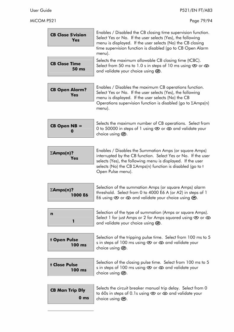
User Guide P521/EN FT/A83 MiCOM P521 Page 79/94
CB Close S'vision Yes
Enables / Disabled the CB closing time supervision function. Select Yes or No. If the user selects (Yes), the following menu is displayed. If the user selects (No) the CB closing time supervision function is disabled (go to CB Open Alarm menu).
CB Close Time 50 ms
Selects the maximum allowable CB closing time (tCBC). Select from 50 ms to 1.0 s in steps of 10 ms using or and validate your choice using .
CB Open Alarm? Yes
Enables / Disables the maximum CB operations function. Select Yes or No. If the user selects (Yes), the following menu is displayed. If the user selects (No) the CB Operations supervision function is disabled (go to ΣAmps(n) menu).
CB Open NB = 0
Selects the maximum number of CB operations. Select from 0 to 50000 in steps of 1 using or and validate your choice using .
ΣAmps(n)? Yes
Enables / Disables the Summation Amps (or square Amps) interrupted by the CB function. Select Yes or No. If the user selects (Yes), the following menu is displayed. If the user selects (No) the CB ΣAmps(n) function is disabled (go to t Open Pulse menu).
ΣAmps(n)? 1000 E6
Selection of the summation Amps (or square Amps) alarm threshold. Select from 0 to 4000 E6 A (or A2) in steps of 1 E6 using or and validate your choice using .
n
1
Selection of the type of summation (Amps or square Amps). Select 1 for just Amps or 2 for Amps squared using or and validate your choice using .
t Open Pulse 100 ms
Selection of the tripping pulse time. Select from 100 ms to 5 s in steps of 100 ms using or and validate your choice using .
t Close Pulse 100 ms
Selection of the closing pulse time. Select from 100 ms to 5 s in steps of 100 ms using or and validate your choice using .
CB Man Trip Dly
0 ms
Selects the circuit breaker manual trip delay. Select from 0 to 60s in steps of 0.1s using or and validate your choice using .
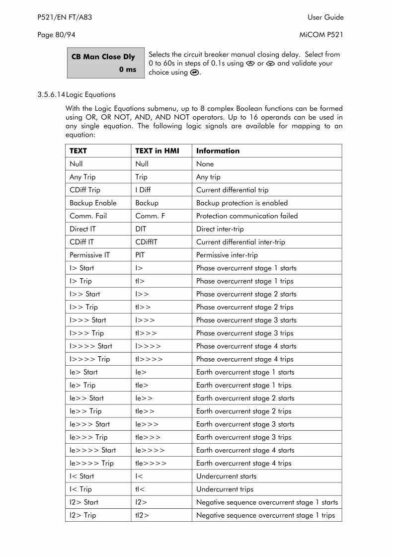
P521/EN FT/A83 User Guide Page 80/94 MiCOM P521
CB Man Close Dly
0 ms
Selects the circuit breaker manual closing delay. Select from 0 to 60s in steps of 0.1s using or and validate your choice using .
3.5.6.14 Logic Equations
With the Logic Equations submenu, up to 8 complex Boolean functions can be formed using OR, OR NOT, AND, AND NOT operators. Up to 16 operands can be used in any single equation. The following logic signals are available for mapping to an equation:
TEXT TEXT in HMI Information
Null Null None
Any Trip Trip Any trip
CDiff Trip I Diff Current differential trip
Backup Enable Backup Backup protection is enabled
Comm. Fail Comm. F Protection communication failed
Direct IT DIT Direct inter-trip
CDiff IT CDiffIT Current differential inter-trip
Permissive IT PIT Permissive inter-trip
I> Start I> Phase overcurrent stage 1 starts
I> Trip tI> Phase overcurrent stage 1 trips
I>> Start I>> Phase overcurrent stage 2 starts
I>> Trip tI>> Phase overcurrent stage 2 trips
I>>> Start I>>> Phase overcurrent stage 3 starts
I>>> Trip tI>>> Phase overcurrent stage 3 trips
I>>>> Start I>>>> Phase overcurrent stage 4 starts
I>>>> Trip tI>>>> Phase overcurrent stage 4 trips
Ie> Start Ie> Earth overcurrent stage 1 starts
Ie> Trip tIe> Earth overcurrent stage 1 trips
Ie>> Start Ie>> Earth overcurrent stage 2 starts
Ie>> Trip tIe>> Earth overcurrent stage 2 trips
Ie>>> Start Ie>>> Earth overcurrent stage 3 starts
Ie>>> Trip tIe>>> Earth overcurrent stage 3 trips
Ie>>>> Start Ie>>>> Earth overcurrent stage 4 starts
Ie>>>> Trip tIe>>>> Earth overcurrent stage 4 trips
I< Start I< Undercurrent starts
I< Trip tI< Undercurrent trips
I2> Start I2> Negative sequence overcurrent stage 1 starts
I2> Trip tI2> Negative sequence overcurrent stage 1 trips

User Guide P521/EN FT/A83 MiCOM P521 Page 81/94
TEXT TEXT in HMI Information
I2>> Start I2>> Negative sequence overcurrent stage 2 starts
I2>> Trip tI2>> Negative sequence overcurrent stage 2 trips
Thermal Alarm Th Alar Thermal overload alarm
Thermal Trip Th Trip Thermal overload trips
CB Alarm CB Alar CB status discrepancy
52 Fail 52 Fail Trip circuit alarm
Broken Cond. Brk Co. Broken conductor protection trips
CB Fail CB Fail CB failure
CB Close CB Clos CB Close
Aux1 Trip tAux1 Auxiliary timer1 trips
Aux2 Trip tAux2 Auxiliary timer2 trips
Active Group Act Grp =1 when active setting group is group 2
TCS Block TCS Blk Trip circuit supervision block operates
Input 1 Input 1 Input 1
Input 2 Input 2 Input 2
Input 3 Input 3 Input 3
Input 4 Input 4 Input 4
Input 5 Input 5 Input 5
Equ A Equ A Logic equation A signal
Equ B Equ B Logic equation B signal
Equ C Equ C Logic equation C signal
Equ D Equ D Logic equation D signal
Equ E Equ E Logic equation E signal
Equ F Equ F Logic equation F signal
Equ G Equ G Logic equation G signal
Equ H Equ H Logic equation H signal
Prgm IT 1 I-Trip1 Programmable inter-trip signal 1
Prgm IT 2 I-Trip2 Programmable inter-trip signal 2
Prgm IT 3 I-Trip3 Programmable inter-trip signal 3
Prgm IT 4 I-Trip4 Programmable inter-trip signal 4
CTS Local Alarm CTS L CT fail alarm local
CTS Remote Alarm
CTS R CT fail alarm remote
CTS Block CTS Blk CT fail block relevant protections
CTS Restrain CTS Res CT fail restraint differential protection
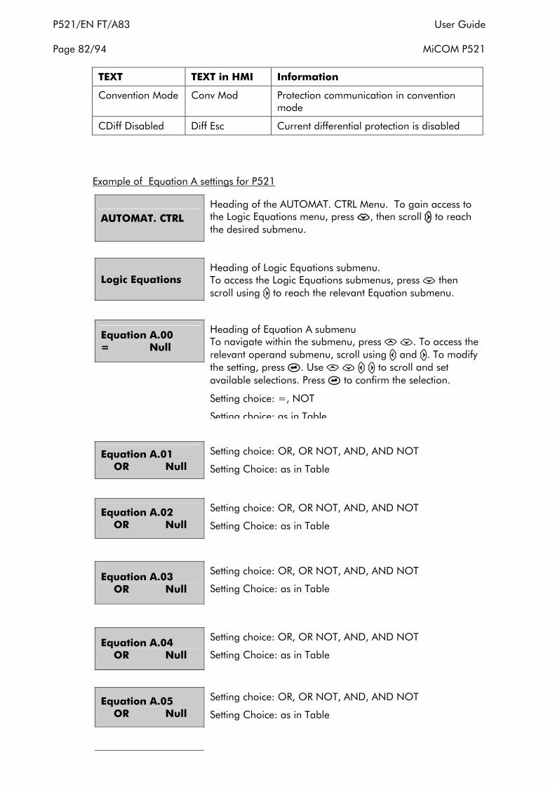
P521/EN FT/A83 User Guide Page 82/94 MiCOM P521
TEXT TEXT in HMI Information
Convention Mode Conv Mod Protection communication in convention mode
CDiff Disabled Diff Esc Current differential protection is disabled
Example of Equation A settings for P521
AUTOMAT. CTRL Heading of the AUTOMAT. CTRL Menu. To gain access to the Logic Equations menu, press , then scroll to reach the desired submenu.
Logic Equations Heading of Logic Equations submenu. To access the Logic Equations submenus, press then scroll using to reach the relevant Equation submenu.
Equation A.00 = Null
Heading of Equation A submenu To navigate within the submenu, press . To access the relevant operand submenu, scroll using and . To modify the setting, press . Use to scroll and set available selections. Press to confirm the selection.
Setting choice: =, NOT
Setting choice: as in Table
Equation A.01 OR Null
Setting choice: OR, OR NOT, AND, AND NOT
Setting Choice: as in Table
Equation A.02 OR Null
Setting choice: OR, OR NOT, AND, AND NOT
Setting Choice: as in Table
Equation A.03 OR Null
Setting choice: OR, OR NOT, AND, AND NOT
Setting Choice: as in Table
Equation A.04 OR Null
Setting choice: OR, OR NOT, AND, AND NOT
Setting Choice: as in Table
Equation A.05 OR Null
Setting choice: OR, OR NOT, AND, AND NOT
Setting Choice: as in Table
User Guide P521/EN FT/A83 MiCOM P521 Page 83/94
Equation A.06 OR Null
Setting choice: OR, OR NOT, AND, AND NOT
Setting Choice: as in Table
Equation A.07 OR Null
Setting choice: OR, OR NOT, AND, AND NOT
Setting Choice: as in Table
Equation A.08 OR Null
Setting choice: OR, OR NOT, AND, AND NOT
Setting Choice: as in Table
Equation A.09 OR Null
Setting choice: OR, OR NOT, AND, AND NOT
Setting Choice: as in Table
Equation A.10 OR Null
Setting choice: OR, OR NOT, AND, AND NOT
Setting Choice: as in Table
Equation A.11 OR Null
Setting choice: OR, OR NOT, AND, AND NOT
Setting Choice: as in Table
Equation A.12 OR Null
Setting choice: OR, OR NOT, AND, AND NOT
Setting Choice: as in Table
Equation A.13 OR Null
Setting choice: OR, OR NOT, AND, AND NOT
Setting Choice: as in Table
Equation A.14 OR Null
Setting choice: OR, OR NOT, AND, AND NOT
Setting Choice: as in Table
Equation A.15 OR Null
Setting choice: OR, OR NOT, AND, AND NOT
Setting Choice: as in Table

P521/EN FT/A83 User Guide Page 84/94 MiCOM P521
3.5.6.15 Program. I-Trip Sub menu
This sub menu makes it possible to assign functions to any of the 4 inter-trip commands, to initiate an inter-trip to the remote relay without additional wiring of logic inputs or output relays.
The available selections are shown in the following table:
Label abstract Label signification
tI> Phase overcurrent stage 1 trips
tI>> Phase overcurrent stage 2 trips
tI>>> Phase overcurrent stage 3 trips
tI>>>> Phase overcurrent stage 4 trips
tIe> Earth overcurrent stage 1 trips
tIe>> Earth overcurrent stage 2 trips
tIe>>> Earth overcurrent stage 3 trips
tIe>>>> Earth overcurrent stage 4 trips
tI< Undercurrent trips
tI2> Negative sequence overcurrent stage 1 trips
tI2>> Negative sequence overcurrent stage 2 trips
CB Fail CB fail operates
Broken Cond. Broken conductor trips
tAux1 Auxiliary timer 1 trips
tAux2 Auxiliary timer 2 trips
Input 1 Logic input 1
Input 2 Logic input 2
Input 3 Logic input 3
Input 4 Logic input 4
Input 5 Logic input 5
Equ A Logic equation A operates
Equ B Logic equation B operates
Equ C Logic equation C operates
Equ D Logic equation D operates
Equ E Logic equation E operates
Equ F Logic equation F operates
Equ G Logic equation G operates
Equ H Logic equation H operates
In addition to the input allocation the user can specify the required dwell time for programmable inter-trip command 1 to 4.

User Guide P521/EN FT/A83 MiCOM P521 Page 85/94
AUTOMAT. CTRL Heading of the AUTOMAT. CTRL Menu. To gain access to the Program. I-Trip Functions menu, press , followed by 16 times.
Program. I-Trip Heading of the Program. I-Trip sub menu. To gain access to the sub menu points, press .
Program. I-Trip1 Heading of the Program. I-Trip 1 sub menu. To gain access to the sub menu points, press .
Program. I-Trip2 Heading of the Program. I-Trip 2 sub menu. To gain access to the sub menu points, press .
Program. I-Trip3 Heading of the Program. I-Trip 3 sub menu. To gain access to the sub menu points, press .
Program. I-Trip4 Heading of the Program. I-Trip 4 sub menu. To gain access to the sub menu points, press .
Dwell Timer
100ms
Set the dwell timer for the inter-trip command. To adjust the time, press . The dwell time is adjustable from 0.1s to 5s in steps of 0.05s. Validate your choice using .
3.5.6.16 CT Supervision Sub menu
The CT Supervision sub menu makes it possible to enable the current transformer supervision function and the various settings associated with this function.
AUTOMAT. CTRL Heading of the AUTOMAT. CTRL Menu. To gain access to the CT Supervision menu, press , , 6 times, , followed by 18 times.
CT Supervision Heading of the CB Supervision sub menu.
To gain access to the sub menu points, press .
CTS? No
Enables / Disables the current transformer supervision function. Select Yes or No. If the user selects (Yes), the function is active. If the user selects (No) the CT supervision is disabled.

P521/EN FT/A83 User Guide Page 86/94 MiCOM P521
CTS Reset mode Manual
Selects the CTS reset mode. Select from Manual or Auto using or and validate your choice using .
CTS Reset RST = [C]
To clear the CTS alarm, press .
CTS I1> 0.1IN
Selects the CTS positive current threshold for local current. Select from 0.05In to 4In in steps of 0.01In using or and validate your choice using .
CTS I2/I1> 5%
Selects the CTS low positive/negative current ratio threshold. Select from 5% to 100% in steps of 5% using or and validate your choice using .
CTS I2/I1>> 40%
Selects the CTS high positive/negative current ratio threshold. Select from 5% to 100% in steps of 5% using or and validate your choice using .
CTS TIME DLY 5.0s
Selects the time delay for raising CTS alarm. Select from 0 to 10s in steps of 0.01s using or and validate your choice using .
CTS Restrain ? No
Enables / Disables the restraint function of current differential protection when a CT failure is detected. Select Yes or No by press , followed by or and validate your choice using .
3.5.7 Records menu
The RECORDS menu makes it possible to read the various records generated by the relay The various sub menus are:
⇒ CB Monitoring
⇒ Fault Record
⇒ Instantaneous
⇒ Disturb Record
⇒ Time Peak Value
⇒ Rolling Demand
To gain access to the RECORDING menu, press then 7 times.

User Guide P521/EN FT/A83 MiCOM P521 Page 87/94
3.5.7.1 CB monitoring sub menu
The CB Monitoring sub menu makes possible to read and clear the parameters and measurements associated to this function.
RECORDS Heading of the RECORD Menu. To gain access to the CB Monitoring menu, press , , 7 times followed by .
CB Monitoring Heading the CB Monitoring sub menu. To gain access to the sub menu points, press .
CB Opening Time 95 ms
Displays the most recent circuit breaker opening time in ms.
CB Closing Time 115 ms
Displays the most recent circuit breaker closing time in ms.
CB Operations RST = [C] 5489
Displays the number of opening commands executed by the circuit breaker. To reset these values, press .
Σ Amps (n) RST = [C]
Allows the user to clear the memorized summation of interrupted currents. All 3 phase currents are clear simultaneously. To clear these values, press .
Σ Amps (n) IA 4 E4
Displays the summation of the Amps (or Amps squared) interrupted by the A phase circuit breaker.
Σ Amps (n) IB 2 E4
Displays the summation of the Amps (or Amps squared) interrupted by the B phase circuit breaker.
Σ Amps (n) IC 8 E3
Displays the summation of the Amps (or Amps squared) interrupted by the C phase circuit breaker.
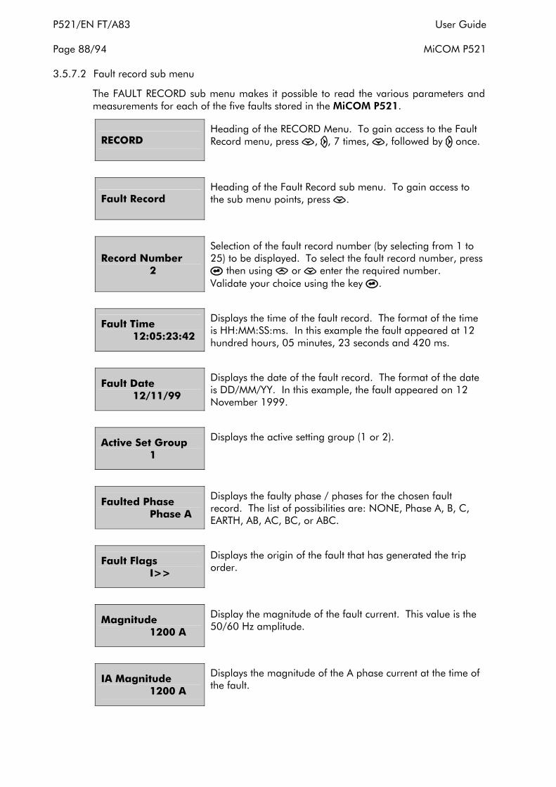
P521/EN FT/A83 User Guide Page 88/94 MiCOM P521
3.5.7.2 Fault record sub menu
The FAULT RECORD sub menu makes it possible to read the various parameters and measurements for each of the five faults stored in the MiCOM P521.
RECORD Heading of the RECORD Menu. To gain access to the Fault Record menu, press , , 7 times, , followed by once.
Fault Record Heading of the Fault Record sub menu. To gain access to the sub menu points, press .
Record Number 2
Selection of the fault record number (by selecting from 1 to 25) to be displayed. To select the fault record number, press
then using or enter the required number. Validate your choice using the key .
Fault Time 12:05:23:42
Displays the time of the fault record. The format of the time is HH:MM:SS:ms. In this example the fault appeared at 12 hundred hours, 05 minutes, 23 seconds and 420 ms.
Fault Date 12/11/99
Displays the date of the fault record. The format of the date is DD/MM/YY. In this example, the fault appeared on 12 November 1999.
Active Set Group 1
Displays the active setting group (1 or 2).
Faulted Phase Phase A
Displays the faulty phase / phases for the chosen fault record. The list of possibilities are: NONE, Phase A, B, C, EARTH, AB, AC, BC, or ABC.
Fault Flags I>>
Displays the origin of the fault that has generated the trip order.
Magnitude 1200 A
Display the magnitude of the fault current. This value is the 50/60 Hz amplitude.
IA Magnitude 1200 A
Displays the magnitude of the A phase current at the time of the fault.

User Guide P521/EN FT/A83 MiCOM P521 Page 89/94
IB Magnitude 500 A
Displays the magnitude of the B phase current at the time of the fault.
IC Magnitude 480 A
Displays the magnitude of the C phase current at the time of the fault.
IN Magnitude 103 A
Displays the magnitude of the earth fault current at the time of the fault.
IA Differential 1200 A
Displays the magnitude of the A phase differential current at the time of the fault.
IB Differential 500 A
Displays the magnitude of the B phase differential current at the time of the fault.
IC Differential 480 A
Displays the magnitude of the C phase differential current at the time of the fault.
Max I Bias 103 A
Displays the largest bias current of the three phases at the time of the fault.
Chann 1 Status Comms OK
Displays the status of the protection comms channel. Relays display either “Comms OK” or Comms Fail”.
3.5.7.3 Instantaneous sub menu
The INSTANTANEOUS sub menu makes is possible to read the various parameters for each of the last five “starts”.
RECORDS Heading of the AUTOMAT. CTRL Menu. To gain access to the CB Monitoring menu, press , , , 7 times, , followed by twice.
Instantaneous Heading of the Instantaneous sub menu.
To gain access to the sub menu points, press .

P521/EN FT/A83 User Guide Page 90/94 MiCOM P521
Number 5
Selection of the Instantaneous record number (by selecting either 1, 2, 3, 4 or 5) to be displayed. To select the Instantaneous record number, press then using or enter the required number. Validate your choice using .
Time 13:07:15:53
Display the time of the instantaneous record. The format is HH:MM:SS:ms. In this example the start information appeared at 13 hundred hours, 07 minutes, 15 seconds and 530 ms.
Date 09/01/01
Display the date of the instantaneous record. The format is DD/MM/YY. In this example the start information appeared on 09 January 2001.
Origin Ie>
Displays the origin of the start signal.
Length 57 ms
Displays the length of the start information.
Trip No
Displays if a trip has occurred due to the start.
3.5.7.4 Disturbance record sub menu
The DISTURBANCE sub menu makes it possible to set the various parameters and thresholds associated with this recording function.
RECORD Heading of the RECORD Menu. To gain access to the Disturbance Record menu, press , , 7 times, , followed by 3 times.
Disturb Record Heading of the Disturb Record sub menu.
To gain access to the sub menu points, press .
Record Number 5
Set the number of disturbance records that the relay can be stored (from 1 to 5). To set the number, press then using
or to input the required number.
Validate your choice using the key .
Pre-Time 100 ms
Selection of the disturbance record pre-trigger time. Select from 100 ms to 3s in steps of 100 ms using or and validate your choice using .

User Guide P521/EN FT/A83 MiCOM P521 Page 91/94
Post-Time 100 ms
Selection of the disturbance record post-trigger time. Select from 100ms to 3s in steps of 100 ms using or and validate your choice using .
WARNING: THE TOTAL DISTURBANCE RECORDING TIME FOR EACH RECORD DEPENDS ON THE NUMBERS OF RECORDS SET.
Disturb Rec Trig ON INST.
Selects the start criteria for the disturbance recorder function. Select between ON INST. (start from instantaneous thresholds) or ON Trip (start from trip conditions) using or and validate your choice using .
3.5.7.5 Time peak value sub menu
The Time Peak Value sub menu makes it possible to set parameters associated with the Peak and Average values displayed in the Measurements menu.
RECORD Heading of the RECORD Menu. To gain access to the Time Peak Value menu, press , , 7 times, , followed by 4 times.
Time Peak Value Heading of the Time Peak Value sub menu. To gain access to the sub menu points, press .
Time Window 5 mn
Selects the length of the time window over which the peak and average values are stored. Select from either 5mn, 10mn, 15mn, 30mn, or 60mn using or and validate your choice using .
3.5.7.6 Rolling demand sub menu
The Rolling Demand sub menu makes it possible to set the rolling sub-period and the number of the sub-periods for the calculation of the 3 phase Rolling Average and Peak Demand values, available in the Measurement menu.
RECORDS Heading of the RECORD Menu. To gain access to the Rolling Demand menu, press , , 7 times, , followed by 5 times.
Rolling Demand Heading of the Rolling Demand sub menu. To gain access to the sub menu points, press .
Sub period 5 mn
Selects the duration of the sub-period during over which the rolling average values are calculated. Select from either 5mn, 10mn, 15mn, 30mn, or 60mn using or and
validate your choice using .

P521/EN FT/A83 User Guide Page 92/94 MiCOM P521
Num of Sub Per 1
Selects the number of sub-periods for the calculation of the average of the average values.

User Guide P521/EN FT/A83 MiCOM P521 Page 93/94
4. WIRING
The connection diagrams for the MiCOM P521 are provided in section P521/EN CO of this Technical Guide.
4.1 Auxiliary supply
The auxiliary supply of the MiCOM P521 relay can be either AC or DC (the ranges are 24-60 Vdc, 24-250 Vdc or 24-240 Vac 50-60 Hz). The auxiliary voltage range is specified on the relay data plate under the upper flap on the front plate. Supply must only be connected to terminals 33 (+ve) and 34 (-ve).
4.2 Current measurement inputs
The MiCOM P521 relay has eight current inputs. The nominal current value of these measuring inputs is either 1 Ampere or 5 Amperes (labeled in the connection diagrams). For the same relay the user can mix the 1 and 5 Ampere inputs between phases and earth.
Note: All phases must have the same rated current value (1 or 5 Amps).
4.3 Logic inputs
The MiCOM P521 relay has 5 opto-isolated logic inputs. Each input is electrically isolated from all other inputs.
Refer to the Technical Data (P521_EN_TD) for the voltage range of the inputs.
The automation operations and signaling functions to which these logic inputs respond can be selected from the AUTOMAT. CTRL Menu.
Note: Do not forget to select in the CONFIGURATION/Configuration Inputs Menu if the voltage input is "AC" or "DC".
4.4 Output relays
Nine output relays are available on MiCOM P521.
The first output relay (RL0) is dedicated to indicate a relay fault (Watchdog). It is normally closed (NC) and cannot be configured.
Relay RL1 is the main trip output. The trip functions which will operate RL1 are selected in the AUTOMAT. CTRL/Trip Commands menu.
RL2 to RL8 are freely programmable. The protection and control functions to which these relays respond can be selected by means of the AUTOMAT. CTRL menu.
RL1 and RL2 have changeover contacts (1 common, 1 normally open contact, 1 normally closed contact). The other relays (RL3 to RL8) are of the normally open (NO) type.
4.5 Communication
4.5.1 EIA(RS)485 rear communication port
All MiCOM relays have an EIA(RS)485 rear communication port.
The connection of communications is allocated to terminals 29-30-31-32, shown in the connection diagrams in section P521/EN CO of this Technical Guide.

P521/EN FT/A83 User Guide Page 94/94 MiCOM P521
4.5.2 EIA(RS)232 front communication port
MiCOM P521 relay provides the user with an EIA(RS)232 communication port. This link is dedicated to the MiCOM Setting software MiCOM S1.
A standard EIA(RS)232 shielded cable should be used to connect the P521 front EIA(RS)232 port to a PC. The connecter on the P521 side must be male in gender.
The wiring of this EIA(RS)232 cable must follow the following scheme.
''*& )
!"#$%&+,#(
&
-
*
.
(
/+,/(
&
-
*
.
(
Figure 4: EIA(RS)232 front port communication cable wiring

Menu Content Tables P521/EN HI/A83 MiCOM P521
MENU CONTENT TABLES
Date: 1st October 2010
Software version: 12
Connection diagrams: 10P52101

P521/EN HI/A83 Menu Content Tables MiCOM P521

Menu Content Tables P521/EN HI/A83 MiCOM P521 Page 1/12
CONTENT
1. MICOM P521 – V12.A SOFTWARE MENU CONTENT 3

P521/EN HI/A83 Menu Content Tables Page 2/12 MiCOM P521

Menu Content Tables P521/EN HI/A83 MiCOM P521 Page 3/12
1. MICOM P521 – V12.A SOFTWARE MENU CONTENT
DE
FA
ULT
DIS
PLA
YΙA
= 1
245
A
Pas
swor
d**
**
Des
crip
tion
P52
1A0E
Z1D
3CA
0
Ref
eren
ceM
iCO
Fre
quen
cy50
Hz
Inpu
t 54
321
Sta
tus
1011
0
OP
P
AR
AM
ET
ER
S
Rel
ay87
6543
21S
tatu
s01
0111
01
Dis
play
Def
ault
Dis
play RM
S Ι
A
Pha
se A
Tex
tL1
Pha
se B
Tex
tL2
Pha
se C
Tex
tL3
E/G
ndTe
xtE
CO
NF
IGU
RA
TIO
N
CT
Rat
ios
Line
CT
prim
ary 10
00
Line
CT
sec
5
LED
5/6
/7/8
Led
Ιdiff
Ιdiff
Fail
B/u
p P
rot.
Com
ms
Fai
lD
irect
I-Tr
ipC
-Diff
I-Tr
ipP
ITΙ> Ι>
>Ι>
>>Ι>
>>>
tΙ>
tΙ>>
tΙ>>
>tΙ
>>>>
Ιe>
Ιe>>
Ιe>>
>Ιe
>>>>
tΙe>
tΙe>
>tΙ
e>>>
tΙe>
>>>
The
rmTr
ipB
rkn.
Con
d.C
B F
ail
tΙ2>
tΙ2>
>In
put 1
Inpu
t 2In
put 3
Inpu
t 4In
put 5
tAux
1tA
ux2
CB
Ala
rmE
quat
ion
A ~
HP
rgm
IT 1
~ 4
CT
S L
ocal
CT
S R
emot
eC
TS
Blo
ckC
TS
Res
trai
nC
onve
ntio
n M
ode
CD
iffD
isab
led
Gro
up S
elec
t
Cha
nge
Gro
upIn
put =
ED
GE
E/G
ndC
T pr
imar
y10
00
E/G
ndC
T se
c5
Sof
twar
e ve
rsio
n12
.A
Dat
e30
/01/
02
Tim
e13
: 57
: 44
Act
ive
Gro
up1
Set
ting
Gro
up1
Ala
rms
Inst
. Sel
f-re
set ?
No
Trip
and
Clo
seN
o O
pera
tion
CT
Cor
rect
Rat
io 1.0
Vec
toria
lCom
p.O
ff
Com
m.F
ail-r
eset
? No
Lang
uage
= EN
GLI
SH
SE
RIA
L N
UM
0000
0002
Dis
turb
Trig
ger
No
CD
iffD
isab
led
Ala
rm?
Yes

P521/EN HI/A83 Menu Content Tables Page 4/12 MiCOM P521
Pha
se R
otat
ion
Pha
se R
otat
ion A-B
-C
ME
AS
UR
EM
EN
TS
Cur
rent
Diff
DE
FA
ULT
DIS
PLA
YΙA
= 1
245
A
Con
figur
atio
n In
puts
CO
NF
IGU
RA
TIO
N
Cur
rent
/Gen
eral
ΙA64
0.10
A
ΙB62
9.00
A
Ι1 =
10
3A
ΙC63
4.50
A
ΙN3.
15A
Inpu
ts
5432
111
111
Ι2 =
50
A
Max
ΙA
RM
S 127.
36A
Max
ΙB
RM
S 156.
28A
Max
ΙC
RM
S 139.
01A
Ave
rage
ΙB R
MS
97.8
8A
MA
X. S
UB
PE
RIO
DΙA
RM
S =
2
45A
MA
X. S
UB
PE
RIO
DΙC
RM
S =
2
50A
Ave
rage
ΙA R
MS
98.2
5A
MA
X. S
UB
PE
RIO
DR
ST
= [C
]
Ave
rage
ΙC R
MS
99.0
2A
MA
X. S
UB
PE
RIO
DΙB
RM
S =
240A
Vol
tage
Inpu
t
= DC
Ther
mal
θR
ST
= [C
]
67%
RA
TIO
Ι2/
ΙI
50%
ΙN -
fnR
ST
= [C
]
0.0
A
Max
& A
vera
geΙ
RS
T =
[C]
Bia
sΙB
629.
00A
Bia
sΙC
634.
50A
Rem
ote
ΙA64
0.10
A
Rem
ote
ΙB62
9.00
A
Rem
ote
ΙC63
4.50
A
Diff
eren
tialΙ
B0A
Diff
eren
tialΙ
C0A
Diff
eren
tialΙ
A0A
Bia
sΙA
640.
10A
RO
LLIN
G A
VE
RA
GE
RS
T =
[C]
RO
LLIN
G A
VE
RA
GE
I A R
MS
=
0.0
0A
RO
LLIN
G A
VE
RA
GE
I B R
MS
=
0.0
0A
RO
LLIN
G A
VE
RA
GE
I C R
MS
=
0.0
0A
Bia
sΙC
634.
50A
Loca
l Ang
leA
-B
120
o
Loca
l Ang
leB
-C
120
o
Loca
l Ang
leC
-A
120
o
Diff
Ang
le A
(L-R
)
0
o
Diff
Ang
le B
(L-R
)
1
o
Diff
Ang
le C
(L-R
)
2
o
Pha
se R
otat
ion
Pha
se R
otat
ion A-B
-C
ME
AS
UR
EM
EN
TS
Cur
rent
Diff
DE
FA
ULT
DIS
PLA
YΙA
= 1
245
A
Con
figur
atio
n In
puts
CO
NF
IGU
RA
TIO
N
Cur
rent
/Gen
eral
ΙA64
0.10
A
ΙB62
9.00
A
Ι1 =
10
3A
ΙC63
4.50
A
ΙN3.
15A
Inpu
ts
5432
111
111
Ι2 =
50
A
Max
ΙA
RM
S 127.
36A
Max
ΙB
RM
S 156.
28A
Max
ΙC
RM
S 139.
01A
Ave
rage
ΙB R
MS
97.8
8A
MA
X. S
UB
PE
RIO
DΙA
RM
S =
2
45A
MA
X. S
UB
PE
RIO
DΙC
RM
S =
2
50A
Ave
rage
ΙA R
MS
98.2
5A
MA
X. S
UB
PE
RIO
DR
ST
= [C
]
Ave
rage
ΙC R
MS
99.0
2A
MA
X. S
UB
PE
RIO
DΙB
RM
S =
240A
Vol
tage
Inpu
t
= DC
Ther
mal
θR
ST
= [C
]
67%
RA
TIO
Ι2/
ΙI
50%
ΙN -
fnR
ST
= [C
]
0.0
A
Max
& A
vera
geΙ
RS
T =
[C]
Bia
sΙB
629.
00A
Bia
sΙC
634.
50A
Rem
ote
ΙA64
0.10
A
Rem
ote
ΙB62
9.00
A
Rem
ote
ΙC63
4.50
A
Diff
eren
tialΙ
B0A
Diff
eren
tialΙ
C0A
Diff
eren
tialΙ
A0A
Bia
sΙA
640.
10A
RO
LLIN
G A
VE
RA
GE
RS
T =
[C]
RO
LLIN
G A
VE
RA
GE
I A R
MS
=
0.0
0A
RO
LLIN
G A
VE
RA
GE
I B R
MS
=
0.0
0A
RO
LLIN
G A
VE
RA
GE
I C R
MS
=
0.0
0A
Bia
sΙC
634.
50A
Loca
l Ang
leA
-B
120
o
Loca
l Ang
leB
-C
120
o
Loca
l Ang
leC
-A
120
o
Diff
Ang
le A
(L-R
)
0
o
Diff
Ang
le B
(L-R
)
1
o
Diff
Ang
le C
(L-R
)
2
o

Menu Content Tables P521/EN HI/A83 MiCOM P521 Page 5/12
ME
AS
UR
EM
EN
TS
Pro
tect
ion
Com
ms
CH
1 V
alid
Msg
s00
CH
1 E
rrM
sgs
00
CH
1 E
rror
edS
ecs
0.05
CH
1 S
evE
rrS
ecs
0.05
CH
1 P
rop
Del
ay 0.05
Ela
psed
Tim
e0.
05
Com
ms
Sta
tsR
ST
= [C
]
Com
mun
icat
ion
Ctr
l Com
ms
Ctr
l Com
ms
?Y
es
Bau
d R
ate 19
200B
d
Par
ityN
one
Sto
p B
its1
Rel
ay A
ddre
ss1
Dat
e fo
rmat P
RIV
AT
E
Not
e: M
enu
for
MO
DB
US
prot
ocol
on
ly.
For m
enus
on
othe
r pro
toco
ls s
ee
Use
r Gui
de (P
521/
EN
FT
), se
ctio
n 3.
5.4.
Pro
tect
ion
Pro
toco
lS
DLC
Dat
a R
ate
64k
Rel
ay A
ddre
ss1A
Clo
ckS
ourc
e C
h1IN
TE
RN
AL
Com
ms
Del
ay T
ol1m
s
Cha
r M
odT
ime
Ιs
Pro
tect
ion
G1/
G2
[87]
Cur
rent
Diff
Ιs1
0.2Ι
n
Ιs2
2.0Ι
n
k130
%
k215
0%
Ιdiff
Del
ay T
ype D
MT
tΙdi
ff0m
s
Ιdiff
Cur
veIE
C S
Ι
Ιdi
ffT
ms
1.0
Ιdi
ffTi
me
Dia
l1.
0
PIT
Tim
e50
ms
PIT
ΙD
isab
leN
o
Cur
rent
Diff
?Y
es
Com
mF
ail T
imer 0m
s
DE
FA
ULT
D
ISP
LAY
ΙA =
124
5A
DIT
Rx
tDw
ell
5.0s
Inru
shO
ptio
nN
o
Hig
h S
et4
IN
PIT
ΙS
elec
tion
Rem
ote
PIT
ΙT
hres
hold 0.
2In
Tra
nsie
ntB
ias
No
DIT
Ala
rmY
es
PIT
Ala
rmY
es
FR
AM
E M
OD
EC
onve
ntio
nC
TS
Is1
1.2
IN
Kr
4
Har
mon
icR
atio 50
%

P521/EN HI/A83 Menu Content Tables Page 6/12 MiCOM P521
[46]
Neg
Seq
OC
Ι2 >
?Y
es
Ι2 >
0.1Ι
n
Ι2 >
Del
ay T
ype
ΙDM
T
Ι2 >
Tm
s0.
025
Ι2 >
Cur
veΙE
C S
Ι
t Res
et60
ms
Ι2>>
0.5Ι
n
Ι2>
> ?
Yes
tΙ2>>
110m
s
[50N
/51N
] E
/Gn
d
Ιe >
?Y
es
Ιe >
0.05
Ιen
Ιe >
Del
ay T
ype ΙD
MT
Ιe >
Tm
s1.
0
t Res
et60
ms
Ιe >
> 1.
0Ιen
tΙe
>>
300m
s
Ιe >
>> ?
Yes
Ιe >
>>1.
0Ιn
tΙe
>>>
100m
s
Ιe >
Cur
veΙE
C S
Ι
Ιe >
> ?
Yes
[49]
Th
erm
OL
The
rmO
L ?
Yes
Ιθ>
0.1Ι
n
Te
10 m
n
θT
rip10
0%
θA
larm
?Y
es
k1.
05
θA
larm
90%
Ιe >
> D
elay
Typ
eD
MT
DE
FA
ULT
DIS
PLA
Y ΙA
= 1
245
A
[50/
51] P
hase
O/C
Ι> ?
Yes
Ι>
1.0Ι
n
Ι>
Del
ay T
ype ID
MT
Ι>
Tm
s1.
0
t Res
et60
ms
Ι>>
10
Ιn
tΙ>>
30
0ms
Ι>>
> ?
Yes
Ι>>
>10
Ιn
tΙ>>
>10
0ms
Ι>
Cur
veIE
C S
Ι
Ι>>
?Y
es
PR
OT
EC
TIO
N
G1/
G2
Ι>>
Del
ay T
ype DM
T
Ι>>
>> ?
Yes
Ι>>
>>10
Ιn
tΙ>>
>>10
0ms
Ιe >
>>>
?Y
es
Ιe >
>>>
1.0Ι
en
tΙe
>>>>
100m
s

Menu Content Tables P521/EN HI/A83 MiCOM P521 Page 7/12
Latc
hF
unct
ions
Latc
hΙd
iffN
o
Latc
hD
irect
Ι-T
rip No
Latc
hC
Diff
Ι-Trip N
o
Latc
htΙ
>N
o
Latc
hP
ΙTN
o
Latc
htΙ
>>N
o
Latc
htΙ
>>>>
No
Latc
htΙ
>>>
No
Latc
htΙ
e >
No
Trip
Com
man
ds
Trip
Ιdiff
Yes
Dire
ct Ι-
Trip
Yes
C D
iffΙ-
Trip
Yes
Trip
tΙ>
Yes
Trip
tΙ>>
Yes
Trip
tΙ>>
>>Y
es
Trip
tΙe
>>Y
es
Trip
tΙe
>>>
Yes
Trip
tΙe
>>>>
Yes
Trip
tΙ<
Yes
PΙT
Yes
Trip
tΙ>>
>Y
es
Latc
htΙe
>>>
No
Latc
htΙe
>>>
>N
o
Latc
htΙ
<N
o
Latc
htΙ
2 >>
No
Latc
hThe
rmal
θ No
Latc
htΙ
2 >
No
Trip
tΙe
>Y
es
DE
FA
ULT
DIS
PLA
Y ΙA
= 1
245
A
[37]
Und
er C
urre
nt
Ι<
?Y
es
Ι<
0.2Ι
n
tΙ<
200m
s
Com
mis
sion
ing N
o
LED
Tes
tN
o
Dis
able
Rel
ays Y
es
PR
OT
EC
TIO
N
G1/
G2
Trip
8765
4321
Tes
t00
0000
00
Con
tact
Tes
tN
o
Dis
able
CB
Sta
ts:
No
Trip
tΙ2
>Y
es
Trip
tΙ2
>>Y
es
Trip
The
rmal
θY
es
AU
TO
MA
T. C
TR
L.
Com
mis
sion
ing
Loop
back
Tes
t Off
ΙDiff
Trip
Fla
gsTrip
:
Latc
htΙ
e >>
No
Trip
Brk
n. C
ond. Y
es
Trip
tAux
1Y
es
Trip
tAux
2Y
es
Latc
htA
ux1
No
Latc
htA
ux2
No
Latc
hB
rkn.
Con
d. No
Trip
TC
S B
lock
Yes
Trip
Equ
A ~
HY
es
Latc
hTC
S B
lock N
o
Latc
hE
quA
~ H
No
Latc
hF
unct
ions
Latc
hΙd
iffN
o
Latc
hD
irect
Ι-T
rip No
Latc
hC
Diff
Ι-Trip N
o
Latc
htΙ
>N
o
Latc
hP
ΙTN
o
Latc
htΙ
>>N
o
Latc
htΙ
>>>>
No
Latc
htΙ
>>>
No
Latc
htΙ
e >
No
Trip
Com
man
ds
Trip
Ιdiff
Yes
Dire
ct Ι-
Trip
Yes
C D
iffΙ-
Trip
Yes
Trip
tΙ>
Yes
Trip
tΙ>>
Yes
Trip
tΙ>>
>>Y
es
Trip
tΙe
>>Y
es
Trip
tΙe
>>>
Yes
Trip
tΙe
>>>>
Yes
Trip
tΙ<
Yes
PΙT
Yes
Trip
tΙ>>
>Y
es
Latc
htΙe
>>>
No
Latc
htΙe
>>>
>N
o
Latc
htΙ
<N
o
Latc
htΙ
2 >>
No
Latc
hThe
rmal
θ No
Latc
htΙ
2 >
No
Trip
tΙe
>Y
es
DE
FA
ULT
DIS
PLA
Y ΙA
= 1
245
A
[37]
Und
er C
urre
nt
Ι<
?Y
es
Ι<
0.2Ι
n
tΙ<
200m
s
Com
mis
sion
ing N
o
LED
Tes
tN
o
Dis
able
Rel
ays Y
es
PR
OT
EC
TIO
N
G1/
G2
Trip
8765
4321
Tes
t00
0000
00
Con
tact
Tes
tN
o
Dis
able
CB
Sta
ts:
No
Trip
tΙ2
>Y
es
Trip
tΙ2
>>Y
es
Trip
The
rmal
θY
es
AU
TO
MA
T. C
TR
L.
Com
mis
sion
ing
Loop
back
Tes
t Off
ΙDiff
Trip
Fla
gsTrip
:
Latc
htΙ
e >>
No
Trip
Brk
n. C
ond. Y
es
Trip
tAux
1Y
es
Trip
tAux
2Y
es
Latc
htA
ux1
No
Latc
htA
ux2
No
Latc
hB
rkn.
Con
d. No
Trip
TC
S B
lock
Yes
Trip
Equ
A ~
HY
es
Latc
hTC
S B
lock N
o
Latc
hE
quA
~ H
No

P521/EN HI/A83 Menu Content Tables Page 8/12 MiCOM P521
Latc
hO
utpu
t Rel
ays
Out
put 2
No
Out
put 3
No
Out
put 4
No
Out
put 6
No
Out
put 5
No
Out
put 7
No
Out
put 8
No
Logi
cS
elec
t 1/2
Sel
1 tΙ
>>N
o
Sel
1 tΙ
>>>
No
Sel
1 tΙ
>>>>
No
Sel
1 tΙ
e>>>
No
Sel
1 tΙ
e>>>
>N
o
Out
put R
elay
s
Sel
1 tΙ
e>>
No
tSel
10m
s
Inpu
ts 1
/2/3
/4/5
DE
FA
ULT
DIS
PLA
Y ΙA
= 1
245
A
Blo
ckin
gLo
gic
1/2
Blo
ck Ι
diff
No
Blo
ck tΙ
>N
o
Blo
ck tΙ
>>N
o
Blo
ck tΙ
2 >>
No
Blo
ck T
herm
al θ N
o
Blo
ck B
rkn.
Con
d. No
AU
TO
MA
T. C
TR
L.
Blo
ck tA
ux1
No
Blo
ck tA
ux2
No
Blo
ck tΙ
>>>
No
Blo
ck tΙ
>>>>
No
Blo
ck tΙ
e >
No
Blo
ck tΙ
e >>
No
Blo
ck tΙ
e >>
>N
o
Blo
ck tΙ
2 >
No
Blo
ck tΙ
e >>
>>N
o
Trip
87
6543
210
0010
0Ιd
iffB
ack-
upP
rot.
Com
ms
Fai
l D
irect
Ι-T
rip
C-d
iffΙ-
Trip
PΙT
Ι> tΙ>
Ι>>
tΙ>>
Ι>>>
tΙ>>
>>Ιe
>tΙ
e>Ιe
>>tΙ
e>>
Ιe>>
>tΙ
e>>>
Ιe>>
>>tΙ
e>>>
>tΙ
<tΙ
2 >
tΙ2
>>Th
erm
Ala
rmTh
erm
Trip
CB
Ala
rm52
Fai
lB
rkn.
Con
d.C
B F
ail
CB
Clo
setA
ux1
tAux
2A
ctiv
e G
roup
TC
S B
lock
Inpu
t1 ~
5E
quA
~ H
Prg
mI-
Trip
1 ~
4C
TS
Loc
alC
TS
Rem
ote
CT
S B
lock
CT
S R
es.
Mod
e C
onve
ntC
Diff
Dis
able
Non
eU
nlat
ch52
a52
bC
B F
ail
Aux
1A
ux2
Blk
Log
1B
lkLo
g 2
Sta
rt D
ist
Col
d L
PU
Log
Sel
1Lo
g S
el 2
Cha
nge
Set
θR
eset
Trip
Circ
Str
ttB
FP
erm
iss
ΙTD
irect
ΙT
Com
ms
RS
TR
emot
eTr
ipR
emot
eC
lose
TC
S B
lock
GP
S S
ync
Res
et L
ED
Inhi
bitC
TS
Aux
1 T
ime
tAux
1
Aux
2 T
ime
tAux
2
Blo
ck E
quat
ion
A ~
HN
o
Inve
rtO
utpu
tR
elay
s
Out
put 2
No
Out
put 3
No
Out
put 4
No
Out
put 6
No
Out
put 5
No
Out
put 7
No
Out
put 8
No

Menu Content Tables P521/EN HI/A83 MiCOM P521 Page 9/12
D
EF
AU
LT D
ISP
LAY
ΙA =
124
5 A
AU
TO
MA
T. C
TR
L.
Bro
ken
Con
duct
or
Brk
n. C
ond.
?Y
es
Brk
n. C
ond.
Tim
etB
C1s
Rat
io Ι2
/Ι120
%
Col
d Lo
adP
UtΙ2
>>
?N
o
Col
d Lo
adP
Ut T
herm
?N
o
Col
d Lo
adP
ULe
vel
200%
Col
d Lo
adP
UtC
L40
0ms
Col
d Lo
adP
U ? N
o
Col
d Lo
adP
UtΙ
> ?
No
Col
d Lo
adP
UtΙ
>> ?
No
Col
d Lo
adP
UtΙ
>>>
?N
o
Col
d Lo
adP
UtΙ
>>>>
?N
o
Col
d Lo
adP
UtΙe
> ?
No
Col
d Lo
adP
U
Col
d Lo
adP
UtΙ
e >>
?N
o
Col
d Lo
adP
UtΙe
>>>
?N
o
Col
d Lo
adP
UtΙ
2 >
?N
o
Col
d Lo
adP
UtΙ
e >>
>> ?
No
CB
Sup
ervi
sion
TC
Sup
ervi
sion
Yes
tTrip
Circ
uit
tSup
200m
s
CB
Ope
n S
’vis
ion
Yes
CB
Clo
se S
’vis
ion
Yes
CB
Ope
n Tim
e 50m
s
CB
Clo
se T
ime
CB
Ope
n N
B =
0
CB
Ope
n A
larm
?Y
es
ΣA
mps
(n) ?
Yes
CB
Fai
l
CB
Fai
l ?N
o
Ι<
= 0.
1Ιn
n1
t Ope
n P
ulse 10
0ms
t Clo
se P
ulse 10
0ms
CB
Fai
l Tim
etB
F10
0ms
Blo
ck Ι
> ?
No
Blo
ck Ιe
> ?
No
ΣA
mps
(n) ? 10
00 E
6
CB
Man
Trip
Dly
0ms
CB
Man
Clo
se D
ly0m
s
DE
FA
ULT
DIS
PLA
Y ΙA
= 1
245
A
AU
TO
MA
T. C
TR
L.
Bro
ken
Con
duct
or
Brk
n. C
ond.
?Y
es
Brk
n. C
ond.
Tim
etB
C1s
Rat
io Ι2
/Ι120
%
Col
d Lo
adP
UtΙ2
>>
?N
o
Col
d Lo
adP
Ut T
herm
?N
o
Col
d Lo
adP
ULe
vel
200%
Col
d Lo
adP
UtC
L40
0ms
Col
d Lo
adP
U ? N
o
Col
d Lo
adP
UtΙ
> ?
No
Col
d Lo
adP
UtΙ
>> ?
No
Col
d Lo
adP
UtΙ
>>>
?N
o
Col
d Lo
adP
UtΙ
>>>>
?N
o
Col
d Lo
adP
UtΙe
> ?
No
Col
d Lo
adP
U
Col
d Lo
adP
UtΙ
e >>
?N
o
Col
d Lo
adP
UtΙe
>>>
?N
o
Col
d Lo
adP
UtΙ
2 >
?N
o
Col
d Lo
adP
UtΙ
e >>
>> ?
No
CB
Sup
ervi
sion
TC
Sup
ervi
sion
Yes
tTrip
Circ
uit
tSup
200m
s
CB
Ope
n S
’vis
ion
Yes
CB
Clo
se S
’vis
ion
Yes
CB
Ope
n Tim
e 50m
s
CB
Clo
se T
ime
CB
Ope
n N
B =
0
CB
Ope
n A
larm
?Y
es
ΣA
mps
(n) ?
Yes
CB
Fai
l
CB
Fai
l ?N
o
Ι<
= 0.
1Ιn
n1
t Ope
n P
ulse 10
0ms
t Clo
se P
ulse 10
0ms
CB
Fai
l Tim
etB
F10
0ms
Blo
ck Ι
> ?
No
Blo
ck Ιe
> ?
No
ΣA
mps
(n) ? 10
00 E
6
CB
Man
Trip
Dly
0ms
CB
Man
Clo
se D
ly0m
s

P521/EN HI/A83 Menu Content Tables Page 10/12 MiCOM P521
DE
FA
ULT
DIS
PLA
Y ΙA
= 1
245
A
AU
TO
MA
T. C
TR
L.
Logi
cE
quat
ions
Equ
atio
n A
~ H
Equ
atio
n A
.00
~ 15
=
N
ULL
T O
pera
te=
0 m
s
Pro
gram
. I-T
rip
Dw
ellT
imer
5.0
s
CT S
uper
visi
on
CTS
?N
o
CTS
Res
et M
ode
Man
ual
CTS
Res
etR
ST=[
C]
CTS
I1>
0.1
IN
CTS
I2/I1
>10
%
T R
eset
=0
ms
Pro
gram
. I-T
rip1~
4
tI> tΙ>>
tΙ>>
>tΙ
>>>>
tΙe>
tΙe>
>tΙ
e>>>
tΙe>
>>>
The
rmTrip
tΙ<
tΙ2
>tΙ
2 >>
CB
Fai
lB
rkn.
Con
d.tA
ux1
tAux
2In
put 1
~ 5
Equ
A ~
H
CTS
I2/I1
>>40
%
CTS
TIM
E D
LY 5.0
s
CTS
Res
trai
n? No

Menu Content Tables P521/EN HI/A83 MiCOM P521 Page 11/12
Dis
turb
Rec
ord
Pre
-tim
e10
0ms
Dis
turb
Rec
Trig
On
Inst
ΙN M
agni
tude
103A
ΙA D
iffer
entia
l 1200
A
ΙB D
iffer
entia
l 500A
Inst
anta
neou
s
Num
ber
5
Tim
e12
: 05
: 23
: 42
ΙC D
iffer
entia
l 480A
Tim
e P
eak
Val
ue
Tim
e W
indo
w5m
n
DE
FA
ULT
DIS
PLA
Y ΙA
= 1
245
A
CB
Mon
itorin
g
CB
Ope
ning
Tim
e95
ms
CB
Clo
sing
Tim
e11
5ms
CB
Ope
ratio
nsR
ST
= [C
]54
89
Rec
ord
Num
ber
2
Fau
ltTim
e12
: 05
: 23
: 42
Fau
ltD
ate 12
/11/
99
RE
CO
RD
S
Act
ive
Set
Gro
up1
Fau
lted
Pha
seP
hase
A
Fau
ltF
lags
Ι>>
Dat
e09
/01/
01
Orig
inΙe
>
Leng
th57
ms
Fau
ltR
ecor
d
Mag
nitu
de12
00A
ΙA M
agni
tude 12
00A
ΙC M
agni
tude
480A
ΙB M
agni
tude
500A
ΣA
mps
(n)
RS
T =
[C]
ΣA
mps
(n)
ΙA4E
4
ΣA
mps
(n)
ΙB2E
4
ΣA
mps
(n)
ΙC8E
3
Max
ΙB
ias
103A
Cha
nn1
Sta
tus
Com
ms
OK
Trip
N
o
Rec
ord
Num
ber
5
Rol
ling
Dem
and
Sub
Per
iod
1 m
n
Num
of S
ubP
er 1
Dis
turb
Rec
ord
Pre
-tim
e10
0ms
Dis
turb
Rec
Trig
On
Inst
ΙN M
agni
tude
103A
ΙA D
iffer
entia
l 1200
A
ΙB D
iffer
entia
l 500A
Inst
anta
neou
s
Num
ber
5
Tim
e12
: 05
: 23
: 42
ΙC D
iffer
entia
l 480A
Tim
e P
eak
Val
ue
Tim
e W
indo
w5m
n
DE
FA
ULT
DIS
PLA
Y ΙA
= 1
245
A
CB
Mon
itorin
g
CB
Ope
ning
Tim
e95
ms
CB
Clo
sing
Tim
e11
5ms
CB
Ope
ratio
nsR
ST
= [C
]54
89
Rec
ord
Num
ber
2
Fau
ltTim
e12
: 05
: 23
: 42
Fau
ltD
ate 12
/11/
99
RE
CO
RD
S
Act
ive
Set
Gro
up1
Fau
lted
Pha
seP
hase
A
Fau
ltF
lags
Ι>>
Dat
e09
/01/
01
Orig
inΙe
>
Leng
th57
ms
Fau
ltR
ecor
d
Mag
nitu
de12
00A
ΙA M
agni
tude 12
00A
ΙC M
agni
tude
480A
ΙB M
agni
tude
500A
ΣA
mps
(n)
RS
T =
[C]
ΣA
mps
(n)
ΙA4E
4
ΣA
mps
(n)
ΙB2E
4
ΣA
mps
(n)
ΙC8E
3
Max
ΙB
ias
103A
Cha
nn1
Sta
tus
Com
ms
OK
Trip
N
o
Rec
ord
Num
ber
5
Rol
ling
Dem
and
Sub
Per
iod
1 m
n
Num
of S
ubP
er 1

P521/EN HI/A83 Menu Content Tables Page 12/12 MiCOM P521
Technical Data and Curve P521/EN TD/A83 Characteristics MiCOM P521
TECHNICAL DATA AND CURVE CHARACTERISTICS
Date: 1st October 2010
Software Version: 12
Connection Diagrams: 10P52101

P521/EN TD/A83 Technical Data and Curve Characteristics MiCOM P521

Technical Data and Curve P521/EN TD/A83 Characteristics MiCOM P521 Page 1/46
CONTENTS
1. PROTECTION FUNCTIONS 5 1.1 Current differential protection 5 1.2 Phase overcurrent protection 6 1.3 Neutral/ground/earth overcurrent protection 7 1.4 Thermal overload protection 10 1.5 Undercurrent protection 10 1.6 Negative sequence overcurrent protection 10
2. AUTOMATION FUNCTIONS 12 2.1 Cold load pickup 12 2.2 Auxiliary timers 12 2.3 Broken conductor detection 12 2.4 Circuit breaker failure 12 2.5 Trip circuit supervision 12 2.6 Circuit breaker control and monitoring 12 2.7 Logic selectivity 13
3. RECORDING FUNCTIONS 13 3.1 Event recorder 13 3.2 Fault recorder 13 3.3 Instantaneous recorder 13 3.4 Disturbance recorder 14
4. RELAY COMMUNICATIONS 14
5. PROTECTION COMMUNICATIONS 14 5.1 Propagation delays 15 5.1.1 Maximum allowable propagation delay 15 5.1.2 Maximum propagation delay difference between send and receive communications
paths 15
6. INPUTS AND OUTPUTS 16 6.1 AC inputs 16 6.2 Logic inputs and outputs 16 6.3 Power supply 17
7. ACCURACY 18
8. CT DATA 18
9. HIGH VOLTAGE WITHSTAND 19

P521/EN TD/A83 Technical Data and Curve Characteristics Page 2/46 MiCOM P521
9.1 Dielectric withstand 19 9.2 Impulse 19 9.3 Insulation resistance 19
10. ELECTRICAL ENVIRONMENT 19 10.1 Performance criteria 19 10.1.1 Class A 19 10.1.2 Class B 20 10.1.3 Class C 20 10.2 Auxiliary supply tests, dc interruption, etc. 20 10.2.1 DC voltage interruptions 20 10.2.2 DC voltage fluctuations 20 10.3 AC voltage dips and short interruptions 20 10.3.1 AC voltage short interruptions 20 10.3.2 AC voltage dips 21 10.4 High frequency disturbance 21 10.5 Fast transients 21 10.6 Conducted/radiated emissions 21 10.6.1 Conducted emissions 21 10.6.2 Radiated emissions 21 10.7 Conducted/radiated immunity 22 10.7.1 Conducted immunity 22 10.7.2 Radiated immunity 22 10.7.3 Radiated immunity from digital radio telephones 22 10.8 Electrostatic discharge 22 10.9 Surge immunity 22 10.10 Power frequency magnetic field 23 10.11 Pulse magnetic field immunity 23 10.12 Damped oscillatory magnetic field immunity 23 10.13 Power frequency interference 23 10.14 Surge withstand capability (SWC) 24 10.15 Radiated immunity 24
11. ATMOSPHERIC ENVIRONMENT 24 11.1 Temperature 24 11.2 Humidity 25 11.3 Enclosure protection 25
12. MECHANICAL ENVIRONMENT 25 12.1 Performance criteria 25

Technical Data and Curve P521/EN TD/A83 Characteristics MiCOM P521 Page 3/46
12.1.1 Severity classes 25 12.1.2 Vibration (sinusoidal) 26 12.1.3 Shock and bump 26 12.1.4 Seismic 26
13. EC EMC COMPLIANCE 26
14. EC LVD COMPLIANCE 27
15. BATTERY LIFE 27
16. FREQUENCY RESPONSE 27
17. CURVES 27 17.1 IDMT curves 28 17.1.1 Pick-up IDMT mathematical formula 28 17.1.2 Reset timer IDMT mathematical formula 29 17.1.3 IEC curves 31 17.1.4 RI curves 37 17.1.5 IEEE/ANSI & CO curves 38 17.1.6 Laborelec curve 44 17.2 Thermal overload curves 45 17.2.1 Mathematical formula 45 17.2.2 Tripping curve 46

P521/EN TD/A83 Technical Data and Curve Characteristics Page 4/46 MiCOM P521
FIGURES
Figure 1: Frequency Response 27 Figure 2: IEC & UK curves 31 Figure 3: Short Time Inverse (IEC) 32 Figure 4: Standard Inverse (IEC) 33 Figure 5: Very Inverse (IEC) 34 Figure 6: Extremely Inverse (IEC) 35 Figure 7: Long Time Inverse (UK) 36 Figure 8: RI Curves 37 Figure 9: ANSI/IEEE & CO curves 38 Figure 10: Short Time Inverse (CO2) 39 Figure 11: Moderately Inverse (ANSI/IEEE) 40 Figure 12: Inverse (CO8) 41 Figure 13: Very Inverse (ANSI/IEEE) 42 Figure 14: Extremely Inverse (ANSI/IEEE) 43 Figure 15: Laborele Curve 44 Figure 16: Thermal Overload Tripping curve 46

Technical Data and Curve P521/EN TD/A83 Characteristics MiCOM P521 Page 5/46
1. PROTECTION FUNCTIONS
1.1 Current differential protection
− Current Fundamental only
− Characteristic Standard two slope
Ιs1 0.1 Ιn to 2.0 Ιn, steps of 0.05 Ιn
Default value 0.2 Ιn (see note)
Ιs2 1.0 Ιn to 30.0 Ιn, steps of 0.05 Ιn
Default value 2.0 Ιn (see note)
k1 0% to 150%, steps of 5%
Default value 30% (see note)
k2 30% to 150%, steps of 5%
Default value 150% (see note)
Note: Use of default setting values is recommended.
− Hysteresis 75%
− Instantaneous Time < 45 ms + signaling delays *
Note: Valid for X/R ratios up to 120 and fault levels between 0.5 In and 25 In
− Drop-off Time < 60 ms + signaling delays *
Note: Valid for X/R ratios up to 120 and fault levels between 0.5 In and 25 In
− Time Delays:
DMT
IDMT Curves:
Time Multiplier Setting (TMS)
0 s to 150 s, steps of 0.01 s
IEC:
Short Time Inverse (IEC),
Standard Inverse (IEC),
Very Inverse (IEC),
Extremely Inverse (IEC),
Long Time Inverse (UK).
0.025 to 1.5, steps of 0.025
Time Dial Setting (TD)
IEEE/ANSI:
Short Time Inverse (CO2),
Moderately Inverse (ANSI),
Inverse (CO8),
Very Inverse (ANSI),
Extremely Inverse (ANSI).
0.1 to 100, steps of 0.1

P521/EN TD/A83 Technical Data and Curve Characteristics Page 6/46 MiCOM P521
IDMT Curve Tolerance
±2% (or 50 ms whichever is greater) at greater than 2 Ιs1.
−
Intertrip Operating Times
Permissive Intertrip Time
Direct Intertrip Time
Current Differential Intertrip Time
≤ 15 ms + PIT Time + signaling delay *
≤ 15 ms + signaling delay *
≤ 5 ms + signaling delay *
* Refer to Accuracy section for calculation of signaling delays.
1.2 Phase overcurrent protection
− Current Fundamental only
− Current Range 0.1 to 40 x rated current, steps of 0.01 Ιn
− Thresholds 4 Independent (Ι>, Ι>>, Ι>>>, Ι>>>>)
0.1 Ιn to 25 Ιn (see note)
Ι>> 0.5 Ιn to 40 Ιn (see note)
Ι>>> 0.5 Ιn to 40 Ιn
Ι>>>> 0.5 Ιn to 40 Ιn
Note: When Ι> or Ι>> is associated with an IDMT curve, the maximum setting recommended should be 2.0 Ιn.
− Hysteresis 95%
− Instantaneous Time < 40 ms
− Drop-off Time < 30 ms
− Time Delays:
DMT
IDMT Curves:
Time Multiplier Setting (TMS)
(tΙ>, tΙ>>, tΙ>>>, tΙ>>>>)
0 s to 150 s, steps of 0.01 s
IEC:
Short Time Inverse (IEC),
Standard Inverse (IEC),
Very Inverse (IEC),
Extremely Inverse (IEC),
Long Time Inverse (UK).
0.025 to 1.5, steps of 0.025
IEEE/ANSI:
Short Time Inverse (CO2),
Moderately Inverse (ANSI),
Inverse (CO8),
Very Inverse (ANSI),
Extremely Inverse (ANSI).
Technical Data and Curve P521/EN TD/A83 Characteristics MiCOM P521 Page 7/46
Time Dial Setting (TD) 0.1 to 100, steps of 0.1
RI:
K Factor Setting (K)
IDMT Curve Tolerance
Electromechanical Type
0.1 to 10, steps of 0.005
±2% (or 50 ms whichever is greater) at >2 Ιn
−
−
Reset Time
IEEE Time Delay:
RTMS
DMT
IEC Time Delay:
DMT
Transient Overreach
Stages 1 & 2 (Ι> & Ι>>)
Stages 3 & 4 (Ι>>> & Ι>>>>)
0.025 to 3.2, steps of 0.025
0.04 s to 100 s, steps of 0.01 s
0.04 s to 100 s, steps of 0.01 s
< 4% for X/R ratios up to 90
< 12% for X/R ratios up to 90
1.3 Ground/earth overcurrent protection
− Current Fundamental only
− Current Ranges 0.002 to 1 x rated current, steps of 0.001 Ιen
0.01 to 8 x rated current, steps of 0.005 Ιen
0.1 to 40 x rated current, steps of 0.005 Ιen

P521/EN TD/A83 Technical Data and Curve Characteristics Page 8/46 MiCOM P521
− Thresholds:
Range:
Range:
Range:
4 Independent (Ιe>, Ιe>>, Ιe>>>, Ιe>>>>)
0.002 to 1 x Ιen
Ιe> 0.002 Ιen to 1Ιen (see note 1)
Ιe>> 0.002 Ιen to 1Ιen (see note 1)
Ιe>>> 0.002 Ιen to 1 Ιen
Ιe>>>> 0.002 Ιen to 1 Ιen
0.01 to 8 x Ιen
Ιe> 0.01 Ιen to 1 Ιen (see note 2)
Ιe>> 0.01 Ιen to 8 Ιen (see note 2)
Ιe>>> 0.01 Ιen to 8 Ιen
Ιe>>>> 0.01 Ιen to 8 Ιen
0.1 to 40 x Ιen
Ιe> 0.1 Ιen to 25 Ιen (see note 2)
Ιe>> 0.5 Ιen to 40 Ιen (see note 2)
Ιe>>> 0.5 Ιen to 40 Ιen
Ιe>>>> 0.5 Ιen to 40 Ιen
Note 1: When Ιe> or Ιe>> is associated with an IDMT curve the maximum setting recommended should be 0.05 Ιen.
Note 2: When Ιe> or Ιe>> is associated with an IDMT curve, the maximum setting recommended should be the maximum of the range / 20.
− Hysteresis 95%
− Instantaneous Time < 40 ms
− Drop-off Time < 30 ms

Technical Data and Curve P521/EN TD/A83 Characteristics MiCOM P521 Page 9/46
− Time Delays:
DMT
IDMT Curves:
Time Multiplier Setting (TMS)
Time Dial Setting (TD)
RI:
K Factor Setting (K)
LABORELEC:
IDMT Curve Tolerance
(tΙe>, tΙe>>, tΙe>>>, tΙe>>>>)
0 s to 150 s, steps of 0.01 s
IEC:
Short Time Inverse (IEC),
Standard Inverse (IEC),
Very Inverse (IEC),
Extremely Inverse (IEC),
Long Time Inverse (UK).
0.025 to 1.5, steps of 0.025
IEEE/ANSI:
Short Time Inverse (CO2),
Moderately Inverse (ANSI),
Inverse (CO8),
Very Inverse (ANSI),
Extremely Inverse (ANSI).
0.1 to 100, steps of 0.1
Electromechanical Type
0.1 to 10, steps of 0.005
Curves 1, 2 and 3 (0.01 to 8 Range only)
±2% (or 50 ms whichever is greater) at >2 Ιen
− Reset Time
IEEE Time Delay:
RTMS
DMT
IEC Time Delay:
DMT
0.025 to 3.2, steps of 0.025
0.04 s to 100 s, steps of 0.01 s
0.04 s to 100 s, steps of 0.01 s

P521/EN TD/A83 Technical Data and Curve Characteristics Page 10/46 MiCOM P521
− Transient Over-reach
Figures quoted are for X/R ratios up to 90
0.1 to 40 Ιn earth fault board:
Stages 1 & 2 (Ιe> & Ιe>>)
Stages 3 & 4 (Ιe>>> & Ιe>>>>)
0.01 to 80 Ιn earth fault board:
Stages 1 & 2 (Ιe> & Ιe>>)
Stages 3 & 4 (Ιe>>> & Ιe>>>>)
0.002 to 1 Ιen earth fault board:
Stages 1 & 2 (Ιe> & Ιe>>)
Stages 3 & 4 (Ιe>>> & Ιe>>>>)
< 4%
< 12%
< 3%
< 12% < 2 %
< 5%
1.4 Thermal overload protection
− Current RMS
− Current Threshold (Ιθ>) 0.1 to 3.2 x rated current, steps of 0.01
− Thermal State (alarm and trip)
50% to 200% x θ, steps of 1%
− Constant Time (Te) 1 min to 200 mins, steps of 1 min
− K Factor 1 to 1.5, steps of 0.01
1.5 Undercurrent protection
− Current Fundamental only
− Phase Current Range (Ι<) 2% to 100% x rated current, steps of 1%
− Time Delay (tΙ<) 0 s to 150 s, steps of 0.01 s
− Hysteresis 105%
1.6 Negative sequence overcurrent protection
− Current Fundamental only
− Current Range 0.1 to 40 x rated current, steps of 0.01 Ιn
− Thresholds 2 Independent (Ι2>, Ι2>>)
Ι2> 0.1Ιn to 40 Ιn (see note)
Ι2>> 0.1Ιn to 40 Ιn
Note: When Ι2> is associated with an IDMT curve the maximum setting 6 recommended should be 2 Ιn.
− Hysteresis 95%
− Instantaneous Time < 40 ms
− Drop-off Time < 30 ms
Technical Data and Curve P521/EN TD/A83 Characteristics MiCOM P521 Page 11/46
− Time Delays:
DMT
IDMT Curves:
Time Multiplier Setting (TMS)
Time Dial Setting (TD)
(tΙ2>, tΙ2>>)
0 s to 150 s, steps of 0.01 s
IEC:
Short Time Inverse (IEC),
Standard Inverse (IEC),
Very Inverse (IEC),
Extremely Inverse (IEC),
Long Time Inverse (UK).
0.025 to 1.5, steps of 0.025
IEEE/ANSI:
Short Time Inverse (CO2),
Moderately Inverse (ANSI),
Inverse (CO8),
Very Inverse (ANSI),
Extremely Inverse (ANSI).
0.1 to 100, steps of 0.1
RI:
K Factor Setting (K)
IDMT Curve Tolerance
Electromechanical Type
0.1 to 10, steps of 0.005
±2% (or 50 ms whichever is greater) at default values.
− Reset Time
IEEE Time Delay:
RTMS
DMT
IEC Time Delay:
DMT
0.025 to 3.2, steps of 0.025
0.04 s to 100 s, steps of 0.01 s
0.04 s to 100 s, steps of 0.01 s

P521/EN TD/A83 Technical Data and Curve Characteristics Page 12/46 MiCOM P521
2. AUTOMATION FUNCTIONS
2.1 Cold load pickup
− Range 20% to 500% x nominal settings, steps of 1%
− Time Delay (tCL) 0.1 s to 3600 s, steps of 0.1 s
2.2 Auxiliary timers
− Auxiliary Timer Numbers 2 independent associated to the Logic Inputs Aux 1 and Aux2
− tAux1 & tAux2 Range 0 s to 200 s, steps of 0.01 s
2.3 Broken conductor detection
− Principle Used Ι2/Ι1
− Threshold 20% to 100%, steps of 1%
− Time Delay (tBC) 1 s to 14400 s, steps of 1 s
2.4 Circuit breaker failure
− Undercurrent Threshold (Ι<) 2% to 100% x rated current, step of 1%
− Threshold Accuracy from 0.02Ιn to 0.1 Ιn :0.006 Ιn
from 0.1 Ιn to 1 Ιn : 2%Ιs
− Threshold Hysteresis Max. 0.008 Ιn or 0.95 Ιs
− CB Failure Time (tBF) 0.03 s to 10 s, steps of 0.01 s
2.5 Trip circuit supervision
− Time Value (tSUP) 0.1 s to 10 s, steps 0.05 s
2.6 Circuit breaker control and monitoring
− CB Opening Time (tOpen) 0.05 s to 1 s, steps of 0.01 s
− CB Closing Time (tClose) 0.05 s to 1 s, steps of 0.01 s
− CB Opening Alarm Threshold
0 to 50000 Operations
− ∑Amps Alarm Threshold 0 to 4x10⁹, steps of 106
− CB Trip Time Alarm Threshold
0.1 s to 5 s, steps of 0.1 s
− CB Close Time Alarm Threshold
0.1 s to 5 s, steps of 0.1 s
Technical Data and Curve P521/EN TD/A83 Characteristics MiCOM P521 Page 13/46
2.7 Logic selectivity
− Timer Number 2 Independent : tSel1 and tSel2
− tSel1 & tSel2 Range 0 to 150 s, steps of 0.01 s
3. RECORDING FUNCTIONS
3.1 Event recorder
− Capacity 75 Events
− Time-Tag to 1 millisecond
− Triggers Any selected Protection Alarm and Threshold
Logic input state change
Self test events
Setting changes
3.2 Fault recorder
− Capacity 5 Faults
− Time-Tag to 1 millisecond
− Triggers Any selected protection alarm and threshold
− Data Stored Fault date
Protection thresholds
Setting group
AC inputs measurements (RMS)
Fault magnitudes
3.3 Instantaneous recorder
− Capacity 5 Starting records (instantaneous threshold pick-up)
− Time-Tag 1 millisecond resolution
− Triggers Any selected phase or earth threshold
− Data Stored Time and date
Origin of fault (threshold)
Duration of the instantaneous flag
Trip (Yes or No)

P521/EN TD/A83 Technical Data and Curve Characteristics Page 14/46 MiCOM P521
3.4 Disturbance recorder
− Capacity 5 Records of up to 3s each
− Sampling Rate 32 Samples per frequency cycle
− Settings: Pre-Time
Post-Time
0.1 s to 3 s. steps of 0.1 s
0.1 s to 3 s. steps of 0.1 s
− Triggers Any selected protection alarm and threshold
Logic input
Remote command
− Data Stored AC Input channels
Digital input/output states
4. RELAY COMMUNICATIONS
− EIA(RS)485 Port:
Connectors
Protocols
Data Rate
Rear Port, Screened Twisted Pair
Screws or Snap-On
MODBUSTM RTU
IEC 60870-5-103
DNP3.0
300 to 38400 Baud (Programmable)
− EIA(RS)232 Port:
Connector
Protocol
Data Rate
Front Port, Screened twisted cable
Sub-D 9 pin female connector
MODBUSTM RTU
19200 Baud
Asynchronous
5. PROTECTION COMMUNICATIONS
− EIA(RS)485 Port:
Connectors
Transmission Mode
Data Rate
Rear Port, Screened twisted pair
Full Duplex Connection
Phoenix Contact model KGG-MC 1,5/ 7
NRZ (recommended)
SDLC
9600 to 64000 Baud (Programmable)
− EIA(RS)232 Port:
Connector
Transmission Mode
Data Rate
Rear Port, Screened twisted cable
Phoenix Contact Model KGG-MC 1,5/ 7
NRZ (recommended)
SDLC
9600 to 64000 Baud (Programmable)
Technical Data and Curve P521/EN TD/A83 Characteristics MiCOM P521 Page 15/46
− Fiber Port:
Connector:
Transmission Mode
Data Rate
850 nm Multi-Mode
1300 nm Multi-Mode
1300 nm Single-Mode
ST Type Fiber Connector
NRZ
SDLC (recommended)
9600 to 64000 Baud (Programmable)
− Errored Secs
Time Available <0.02 ITU-T G.821
− Severe Error Secs
Time Available <0.008 ITU-T G.821
5.1 Propagation delays
5.1.1 Maximum allowable propagation delay
Data Rate System Frequency 9.6 kB/s 19.2 kB/s 56 kB/s 64 kB/s
50 Hz 162 ms 94 ms 29 ms 29 ms
60 Hz 158 ms 80 ms 24 ms 24 ms
5.1.2 Maximum propagation delay difference between send and receive communications paths
Data Rate System Frequency 9.6 kB/s 19.2 kB/s 56 kB/s 64 kB/s
50 Hz 2 ms 2 ms 2 ms 1 ms
60 Hz 1 ms 1 ms 1 ms 1 ms

P521/EN TD/A83 Technical Data and Curve Characteristics Page 16/46 MiCOM P521
6. INPUTS AND OUTPUTS
6.1 AC inputs
− Phase Current Inputs 1 and 5 Amps by connection
− Earth Current Inputs 1 and 5 Amps by connection
− Frequency:
Nominal
Range
50 or 60 Hz by setting selection
Nominal ±5 Hz
− Current Inputs Burden:
Phase
Earth
<0.025 VA (1 A)
<0.3 VA (5 A)
<0.008 VA at 0.1Ιe (1 A)
<0.01 VA for 0.1Ιe (5 A)
− Thermal Withstand 1s @ 100 x Rated Current with 400 A Maximum
2s @ 40 x Rated Current
Continuous @ 4 x Rated Current
6.2 Logic inputs and outputs
Logic input
The logic inputs should be powered with a DC voltage, except for the A, F, T auxiliary voltage range which accepts both DC and AC voltage.
RELAY AUXILIARY POWER SUPPLY
LOGIC INPUT VOLTAGES
Ordering Code (Cortec)
Nominal voltage range
Vx
Operating range
Nominal voltage range
Minimal polarization
voltage
Maximum polarization
current
Holding current
after 2ms
Maximum continuous withstand
A 24 – 60 Vdc 19.2 - 76 Vdc
F 48 - 250 Vdc
48 –240 Vac
38.4 - 300 Vdc
38.4 - 264 Vac
24 – 250 Vdc
24 - 240 Vac
19.2 Vdc
19.2 Vac 35 mA 2.3 mA
300 Vdc
264 Vac
T
48 - 250 Vdc
48 –240 Vac
Special EA (**)
38.4 - 300 Vdc
38.4 - 264 Vac
24 - 250 Vdc
24 - 240 Vac
19.2 Vdc
19.2 Vac 35 mA 2.3 mA
300 Vdc
264 Vac
H 48 - 250 Vdc
48 –240 Vac
38.4 – 300 Vdc
38.4 - 264 Vac 129 Vdc 105 Vdc 3.0 mA @ 129 Vdc 145 Vdc
V 48 - 250 Vdc
48 –240 Vac
38.4 - 300 Vdc
38.4 - 264 Vac 110 Vdc 77 Vdc 7.3 mA @ 110 Vdc 132 Vdc
W 48 - 250 Vdc
48 –240 Vac
38.4 - 300 Vdc
38.4 - 264 Vac 220 Vdc 154 Vdc 3.4 mA @ 220 Vdc 262 Vdc
Z 24 - 250 Vdc
24 - 240 Vac
19.2 - 300 Vdc
19.2 - 264 Vac
24 - 250 Vdc
24 - 240 Vac
19.2 Vdc
19.2 Vac 35 mA 2.3 mA
300 Vdc
264 Vac
(**) Logic input recognition time for EA approval. Dedicated filtering on 24 samples (15 ms at 50 Hz).
Technical Data and Curve P521/EN TD/A83 Characteristics MiCOM P521 Page 17/46
Logic output
− Type Dry Contact Ag CdO
− Rating:
Make
Carry
Break
30 Amps and carry for 3 s
5 Amps continuous
135 Vdc, 0.3 Amps (L/R=30 ms)
250 Vdc, 50 W resistive or 25 W inductive (L/R=40 ms)
220 Vac, 5 Amps (cos ϕ=0.6)
− Operation Time <7 ms
− Mechanical Durability >100 000 Operations
6.3 Power supply
− Auxiliary Voltages, Vaux 24 – 60 Vdc
24 – 250 Vdc/24 – 240 Vac, 50/60 Hz
− Power Supply Variations dc ±20%
ac –20%, +10%
− Ripple 12%
− DC Interruption 50 ms
− Burden 3 W Standby + 0.4 W per Energized Relay + 10 mA per logic input
6 VA Standby + 0.4 VA per Energized Relay + 10 mA per logic input

P521/EN TD/A83 Technical Data and Curve Characteristics Page 18/46 MiCOM P521
7. ACCURACY
− Protection Thresholds ±2% (5% - current differential)
− Time Delay ±2 % with a minimum of 0.05 s
− Measurements Typical ±0.2% at Ιn for measured quantities and 0.5% for derived quantities
− Additional Error Due to Frequency Variation
± Erreur !% between 45 and 65 Hz
where f = actual frequency
fn = nominal frequency (e.g. 50/60 Hz)
− Calculation of Signaling Delay
= ⎩⎪⎨⎪⎧
⎭⎪⎬⎪⎫
2 ⎣⎢⎡
⎦⎥⎤ Integer ⎝⎜
⎛⎠⎟⎞NB/BR ,KF + 1 . KF + Dp
Where:
BR = Baud rate setting (e.g. 9600, 19200, 56000, 64000)
NB = Number of bits in the message (NRZ = 210 bits, SDLC = 204 bits)
Dp = Propagation delay of system (select zero seconds for direct fiber connected systems, or refer to modem configuration section for typical modem propagation delays)
Integer = Nearest whole number (rounded up)
KF = Erreur !
FS = System frequency setting (50 Hz or 60 Hz)
8. CT DATA
− Phase CT Primary 1 to 9999, steps of 1
− Earth CT Primary 1 to 9999, steps of 1
− Phase CT Secondary 1 or 5
− Earth CT Secondary 1 or 5
− CT Correction Factor 0.05 to 2.0, steps of 0.001
− Earth Current Residual Connection or Core Balanced CT (preferred in isolated and compensated neutral systems)
Signaling Delay (in seconds)

Technical Data and Curve P521/EN TD/A83 Characteristics MiCOM P521 Page 19/46
9. HIGH VOLTAGE WITHSTAND
9.1 Dielectric withstand
IEC 60255-5: 2000
2.0 kVrms for one minute between all terminals and case earth (including EIA(RS)485/EIA(RS)232 socket SK1).
2.0 kVrms for one minute between all terminals of each independent circuit grouped together, and all other terminals (including EIA(RS)485/EIA(RS)232 socket SK1).
1.0 kVrms for one minute across dedicated normally open contacts of output relays.
1.0 kVrms for 1 minute across normally open contacts of changeover and watchdog output relays.
9.2 Impulse
IEC 60255-5: 2000
The product will withstand without damage impulses of 5 kV peak, 1.2/50 µs, 0.5J across:
Each independent circuit and the case with the terminals of each independent circuit connected together.
Independent circuits with the terminals of each independent circuit connected together.
Terminals of the same circuit except normally open metallic contacts.
9.3 Insulation resistance
IEC 60255-5: 2000
The insulation resistance is greater than 100 MΩ at 500 Vdc.
10. ELECTRICAL ENVIRONMENT
10.1 Performance criteria
The following three classes of performance criteria are used to specify the performance of the MiCOM relay when subjected to the electrical interference. The performance criteria are based on the performance criteria specified in EN 50082-2:1995.
10.1.1 Class A
During the testing, the relay will not mal-operate and upon completion of testing the relay will function as specified. A mal-operation will include a transient operation of the output contacts, operation of the watchdog contacts, reset of any of the relay’s microprocessors or an alarm indication.
The relay communications must continue uncorrupted via the communications ports during the test, however, relay communications may be momentarily interrupted, provided they recover with no external intervention.

P521/EN TD/A83 Technical Data and Curve Characteristics Page 20/46 MiCOM P521
10.1.2 Class B
During the testing, the relay will not mal-operate and upon completion of the testing, the relay will function as specified. A mal-operation will include a transient operation of the output contacts, operation of the watchdog contacts, reset of any of the relay’s microprocessors or an alarm indication. Transitory operation of the output LEDs is acceptable, provided no permanent false indications are recorded.
The relay communications must continue uncorrupted via the communications ports during the test. However, relay communications may be momentarily interrupted, provided they recover with no external intervention.
10.1.3 Class C
The relay will power down and power up again in a controlled manner within 5 seconds. The output relays are permitted to change state during the test as long as they reset once the relay powers up.
Communications to the relay may be suspended during the testing, as long as communication recovers with no external intervention after the testing.
10.2 Auxiliary supply tests, dc interruption, etc.
10.2.1 DC voltage interruptions
IEC 60255-11: 1979.
DC Auxiliary Supply Interruptions 2, 5, 10, 20, 50 ms.
Performance criteria - Class A.
DC Auxiliary Supply Interruptions 100, 200 ms, 40 s.
Performance criteria - Class C.
10.2.2 DC voltage fluctuations
IEC 60255-11: 1979.
AC 100 Hz ripple superimposed on the DC max. and min. auxiliary supply at 12% of highest rated DC.
Performance criteria - Class A.
10.3 AC voltage dips and short interruptions
10.3.1 AC voltage short interruptions
IEC 61000-4-11: 1994.
AC Auxiliary Supply Interruptions 2, 5, 10, 20, 50 ms.
Performance criteria - Class A.
AC Auxiliary Supply Interruptions 100, 200 ms, 1 s, 40 s.
Performance criteria - Class C.
Technical Data and Curve P521/EN TD/A83 Characteristics MiCOM P521 Page 21/46
10.3.2 AC voltage dips
IEC 61000-4-11: 1994
AC Auxiliary Supply 100% Voltage Dips 2, 5, 10, 20, 50 ms.
Performance criteria - Class A.
AC Auxiliary Supply 100% Voltage Dips 100, 200 ms, 1 s, 40 s.
Performance criteria - Class C.
10.4 High frequency disturbance
IEC 60255-22-1: 1988 Class III.
1 MHz burst disturbance test.
IEC 61000-4-12: 1995 Class III.
100 kHz burst disturbance test.
2.5 kV common mode.
Power supply, CTs, opto inputs, output contacts, rear EIA(RS)485 protection communications port.
1 kV differential mode.
Power supply, CTs, opto inputs and output contacts.
Performance criteria Class A.
10.5 Fast transients
IEC 60255-22-4: 2002 (EN 61000-4-4: 1995), Class III and Class IV.
2 kV 5 kHz (Class III) and 4 kV 2.5 kHz (Class IV) direct coupling.
Power supply, opto inputs, output contacts, CTs.
2 kV 5 kHz (Class III) and 4 kV 2.5 kHz (Class IV) capacitive clamp.
EIA(RS)485 / EIA(RS)232 protection communications port.
Performance criteria Class A.
10.6 Conducted/radiated emissions
10.6.1 Conducted emissions
EN 55022: 1995 Class A, IEC 60255-25: 2000 Class A.
0.15 - 0.5 MHz, 79 dBµV (quasi peak) 66 dBµV (average).
0.5 – 30 MHz, 73 dBµV (quasi peak) 60 dBµV (average).
10.6.2 Radiated emissions
EN 55022: 1995 Class A, IEC 60255-25: 2000 Class A.
30 – 230 MHz, 40 dBµV/m at 10 m measurement distance.
230 – 1000 MHz, 47 dBµV/m at 10 m measurement distance.

P521/EN TD/A83 Technical Data and Curve Characteristics Page 22/46 MiCOM P521
10.7 Conducted/radiated immunity
10.7.1 Conducted immunity
IEC 60255-22-6: 1996/A1 2001, IEC 61000-4-6: 2002 Level 3.
10 V emf @ 1 kHz 80% AM, 150 kHz to 80 MHz. Spot tests at 27 MHz, 68 MHz.
Performance criteria Class A.
10.7.2 Radiated immunity
IEC 60255-22-3: 2000 Class III, IEC 61000-4-3: 1995 Level 3.
10 V/m 80 MHz - 1GHz @ 1 kHz 80% AM.
Spot tests at 80 MHz, 160 MHz, 450 MHz, 900 MHz (10 V/m).
Performance criteria Class A.
10.7.3 Radiated immunity from digital radio telephones
IEC 60255-22-3: 2000 Class III, IEC 61000-4-3: 2002 Class 4.
30 V/m 800 MHz – 960 MHz @ 1 kHz 80% AM.
30 V/m 1.4 GHz - 2.0 GHz @ 1 kHz 80% AM.
10 V/m 900 MHz ± 5 MHz and 1.89 GHz ± 5 MHz, 200 Hz rep. Freq., 50% duty cycle pulse modulated.
Performance criteria Class A.
10.8 Electrostatic discharge
IEC 60255-22-2: 1996 Class 3 & Class 4, IEC 61000-4-2: 1995.
Class 4: 15 kV air discharge (front panel excluding front comms.).
Class 3: 8 kV air discharge (communications port).
Class 3: 6 kV contact discharge (front panel).
Performance criteria Class A.
10.9 Surge immunity
IEC 60255-22-5: 2002, IEC 61000-4-5: 1995 Levels 3 and 4.
Level 4 - AC/DC PSU, CTs, optos, output contacts.
Level 3 - DC PSU, EIA(RS)485 rear protection communications channel.
Performance criteria Class A under reference conditions.

Technical Data and Curve P521/EN TD/A83 Characteristics MiCOM P521 Page 23/46
10.10 Power frequency magnetic field
IEC 61000-4-8: 1993 Level 5.
100 A/m field applied continuously in all planes with the EUT configured in its quiescent and tripping states.
1000 A/m field applied for 3 s in all planes with the EUT configured in its quiescent and tripping states.
Performance criteria Class A.
10.11 Pulse magnetic field immunity
IEC 61000-4-9: 1993 Level 5.
6.4 µs/16 µs magnetic pulse, 1000 A/m, applied in both polarities in each plane with the EUT configured in its quiescent state.
Performance criteria Class A.
10.12 Damped oscillatory magnetic field immunity
IEC 61000-4-10: 1993 Level 5.
0.1 MHz and 1 MHz damped oscillatory pulses, 100 A/m, applied in both polarities in each plane with the EUT configured in its quiescent state.
Performance criteria Class A.
10.13 Power frequency interference
IEC 60255-22-7: 2003
NGTS* 2.13 Issue 1 Dec 2000, section 7.55
EATS 48-5, Issue 2: 2000.
300 Vrms common mode.
250 Vrms differential mode.
Voltage applied to all non-mains frequency inputs. Permanently connected communications circuits tested to Class 3 (100-1000 m) test level 50 mV.
Performance criteria Class A.
* National Grid Technical Specification

P521/EN TD/A83 Technical Data and Curve Characteristics Page 24/46 MiCOM P521
10.14 Surge withstand capability (SWC)
ANSI/IEEE C37.90.1 (2002)
Oscillatory SWC Test
2.5 kV – 3 kV, 1 - 1.5 MHz - common and differential mode - applied to all circuits except for terminal block communications, which are tested common mode only via the cable screen.
Fast Transient SWC Tests
4 – 5 kV crest voltage - common and differential mode - applied to all circuits except for terminal block communications, which are tested common mode only via the cable screen.
Performance criteria Class A
10.15 Radiated immunity
ANSI/IEEE C37.90.2 1995
35 V/m 25 MHz – 1 GHz, no modulation, applied to all sides.
35 V/m 25 MHz – 1 GHz, 100% pulse modulated, to front only.
Performance criteria Class A.
11. ATMOSPHERIC ENVIRONMENT
11.1 Temperature
IEC 60068-2-1: 2007
-25°C storage (96 hours)
-40°C operation (96 hours)
IEC 60068-2-2: 2007
+70°C storage (96 hours)
+85°C operation (96 hours)

Technical Data and Curve P521/EN TD/A83 Characteristics MiCOM P521 Page 25/46
11.2 Humidity
IEC 60068-2-3: 1969
Damp heat, steady state, 40° C ± 2° C and 93% relative humidity (RH) +2% −3%, duration 56 days.
IEC 60068-2-30: 1980
Damp heat cyclic, six (12 + 12 hour cycles) of 55°C ±2°C 93% ±3% RH and 25°C ±3°C 93% ±3% RH.
11.3 Enclosure protection
IEC 60529: 2001
IP52 Category 2
IP5x – Protected against dust, limited ingress permitted.
IPx2 – Protected against vertically falling drops of water with the product in 4 fixed positions of 15° tilt with a flow rate of 3 mm/minute for 2.5 minutes.
12. MECHANICAL ENVIRONMENT
12.1 Performance criteria
The following two classes of performance criteria are used within sections to (where applicable) to specify the performance of the MiCOM relay when subjected to mechanical testing.
12.1.1 Severity classes
The following table details the Class and Typical Applications of the vibration, shock bump and seismic tests detailed previously
Class Typical Application
1 Measuring relays and protection equipment for normal use in power plants, substations and industrial plants and for normal transportation conditions
2
Measuring relays and protection equipment for which a very high security margin is required or where the vibration (shock and bump) (seismic shock) levels are very high, e.g. shipboard application and for severe transportation conditions.
P521/EN TD/A83 Technical Data and Curve Characteristics Page 26/46 MiCOM P521
12.1.2 Vibration (sinusoidal)
IEC 60255-21-1: 1988
Cross over frequency - 58 to 60 Hz
Vibration response
Severity Class
Peak Displacement Below Cross Over Frequency (mm)
Peak Acceleration Above Cross Over
Frequency (gn )
Number of Sweeps in Each Axis
Frequency Range (Hz)
2 0.075 1 1 10 – 150
Vibration endurance
Severity Class Peak Acceleration (gn ) Number of Sweeps
in Each Axis Frequency Range
(Hz)
2 2.0 20 10 – 150
12.1.3 Shock and bump
IEC 60255-21-2: 1988
Type of Test Severity Class
Peak Acceleration ( gn )
Duration of Pulse ( ms )
Number of Pulses in Each
Direction
Shock Response
2 10 11 3
Shock Withstand 1 15 11 3
Bump 1 10 16 1000
12.1.4 Seismic
IEC 60255-21-3: 1993
Cross over frequency - 8 to 9 Hz
x = horizontal axis, y = vertical axis
Peak Displacement Below Cross Over Frequency (mm)
Peak Acceleration Above Cross Over
Frequency (gn) Severity Class
x y x y
Number Of
Sweep Cycles In
Each Axis
Frequency Range (Hz)
2 7.5 3.5 2.0 1.0 1 1- 35
13. EC EMC COMPLIANCE
Compliance to the European Community Directive 89/336/EEC amended by 93/68/EEC is claimed via the Standards route.
The following Product Specific Standard was used to establish conformity:
EN 50263: 2000

Technical Data and Curve P521/EN TD/A83 Characteristics MiCOM P521 Page 27/46
14. EC LVD COMPLIANCE
Compliance with European Community Directive on Low Voltage 73/23/EEC is demonstrated by reference to generic safety standards:
EN 61010-1: 2001
EN 60950-1: 2001
15. BATTERY LIFE (WHEN FITTED IN PHASE 1)
Battery life (assuming relay energized for >90% of time) > 10 years.
16. FREQUENCY RESPONSE
With exception of the RMS measurements and thermal overload protection all other measurements are based upon the Fourier derived fundamental component. The fundamental component is extracted by using a 16 sample Discrete Fourier Transform (DFT). This gives good harmonic rejection for frequencies up to the 15th harmonic. The 15th is the first predominant harmonic that is not attenuated by the fourier filter and is known as an ‘Alias’. The Alias, however, is attenuated by approximately 70% by an additional analogue, ‘anti-aliasing’ filter (low pass filter). The combined affect of the anti-aliasing and fourier filters is shown below.
!
"
Figure 1: Frequency Response

P521/EN TD/A83 Technical Data and Curve Characteristics Page 28/46 MiCOM P521
17. CURVES
17.1 IDMT curves
17.1.1 Pick-up IDMT mathematical formula
Inverse Time Curves Formulae:
The first and second stage phase and earth overcurrent threshold can be selected with a dependent time characteristic. The time delay is calculated with a mathematical formula. There are eleven inverse time characteristics available.
The mathematical formula applicable to the first ten curves is:
t = T x ⎝⎜⎛
⎠⎟⎞
K ,, (Ι/Ιs) α - 1 + L
Where:
t = Operating time (secs)
K = Coefficient (see table)
Ι = Value of measured current
ΙS = Value of the programmed threshold (Pick-up value)
α = Coefficient (see table)
L = ANSI/IEEE coefficient (zero for IEC curves)
T = Time Multiplier Setting (TMS) for IEC curves or Time Dial (TD) for ANSI/IEEE curves.
Type of curve Standard K Factor α Factor L Factor
Short Time Inverse IEC 0.05 0.04 0
Standard Inverse IEC 0.14 0.02 0
Very Inverse IEC 13.5 1 0
Extremely Inverse IEC 80 2 0
Long time Inverse UK 120 1 0
Short Time Inverse CO2 0.02394 0.02 0.01694
Moderately Inverse ANSI/IEEE 0.0515 0.02 0.114
Inverse CO8 5.95 2 0.18
Very Inverse ANSI/IEEE 19.61 2 0.491
Extremely Inverse ANSI/IEEE 28.2 2 0.1215
The RI curve (electromechanical) is given by the following formula:
t = K x ( ) 1,, 0.339 - 0.236 /(Ι/Ιs) when 1.1 < = (Ι/Ιs) < = 20
Although the curves tend towards infinity when the current approaches Ιs, the minimum guaranteed value of the operating current for all the curves with the inverse time characteristic is 1.1 Ιs (with a tolerance of ±0.05 Ιs).

Technical Data and Curve P521/EN TD/A83 Characteristics MiCOM P521 Page 29/46
Laborelec Curves:
The first and second earth thresholds can be selected with dedicated Laborelec curves. There are 3 curves available with the following formula:
t = αΙ + b
Where:
t = Tripping time
α = Coefficient (see table)
b = Coefficient (see table)
Ι = Primary residual current (between 1 and 40A)
Type of Curve α b
LABORELEC 1 – 0.0897 4.0897
LABORELEC 2 – 0.0897 4.5897
LABORELEC 3 – 0.0897 5.0897
In order to be compliant with the Laborelec specifications the relay must be used with:
− An earth current range 0.01 Ιen to 8 Ιen
− A rated current wiring 1 A
− A core balanced CT with a ratio 20/1.
For a complete operating of the curve, the relay must be set to 0.05Ιen (secondary residual current).
17.1.2 Reset timer IDMT mathematical formula
Reset Timer Description:
The first and second phase and earth overcurrent stages are provided with a timer hold facility ‘tReset’, which may be set to a definite time value or to an inverse time characteristic (IEEE/ANSI curves only). This may be useful in certain applications, for example when grading with upstream electromechanical overcurrent relays which have inherent reset time delays.
Another possible situation where the timer hold facility may be used to reduce fault clearance times is where intermittent faults occur. An example of this may occur in a plastic insulated cable. In this application, it is possible that the fault energy melts and reseals the cable insulation, thereby extinguishing the fault. This process repeats to give a succession of fault current pulses, each of increasing duration with reducing intervals between the pulses, until the fault becomes permanent.
When the reset time of the overcurrent relay is minimum the relay will be repeatedly reset and not be able to trip until the fault becomes permanent. By using the Timer Hold facility the relay will integrate the fault current pulses, thereby reducing fault clearance time.
The reset timer ‘tReset’ facility can be found in the following menu configurations:
− If the threshold is selected with an IDMT IEC or RI curve, the reset timer ‘tReset’ with DMT characteristic is settable in the menu and can be found at the following locations:

P521/EN TD/A83 Technical Data and Curve Characteristics Page 30/46 MiCOM P521
− Phase fault reset timer setting:
− Protection → [50/51] Phase OC → tReset
− Earth fault reset timer setting:
− Protection → [50N/51N] E/Gnd → tReset
− If the threshold is selected with an IDMT IEEE or CO curve, the reset timer ‘tReset’ with a DMT or IDMT characteristic is settable in the menu at the following locations:
− Phase fault reset timer setting:
− Protection → [50/51] Phase OC → Reset Type
− Earth fault reset timer setting:
− Protection → [50N/51N] E/Gnd → Reset Type
Inverse Time Curves Formulae:
The mathematical formula applicable to the five curves is:
t = T x ⎝⎛
⎠⎞K ,, 1 - (Ι/Ιs)α
Where:
t = Reset time
K = Coefficient (see table)
Ι = Value of the measured current
ΙS = Value of the programmed threshold (pick-up value)
α = Coefficient (see table)
T = Reset Time Multiplier (Rtms) between 0.025 and 3.2
Type of Curves Standard K Factor α Factor
Short Time Inverse CO2 2.261 2
Moderately Inverse ANSI/IEEE 4.85 2
Inverse CO8 5.95 2
Very Inverse ANSI/IEEE 21.6 2
Extremely Inverse ANSI/IEEE 29.1 2

Technical Data and Curve P521/EN TD/A83 Characteristics MiCOM P521 Page 31/46
17.1.3 IEC curves
P0006ENa
Figure 2: IEC & UK curves
Short Time Inverse
Very Inverse
Long Time Inverse (UK)
Standard Inverse
Extremely Inverse
IEC & UK Curves
(TMS=0,025)
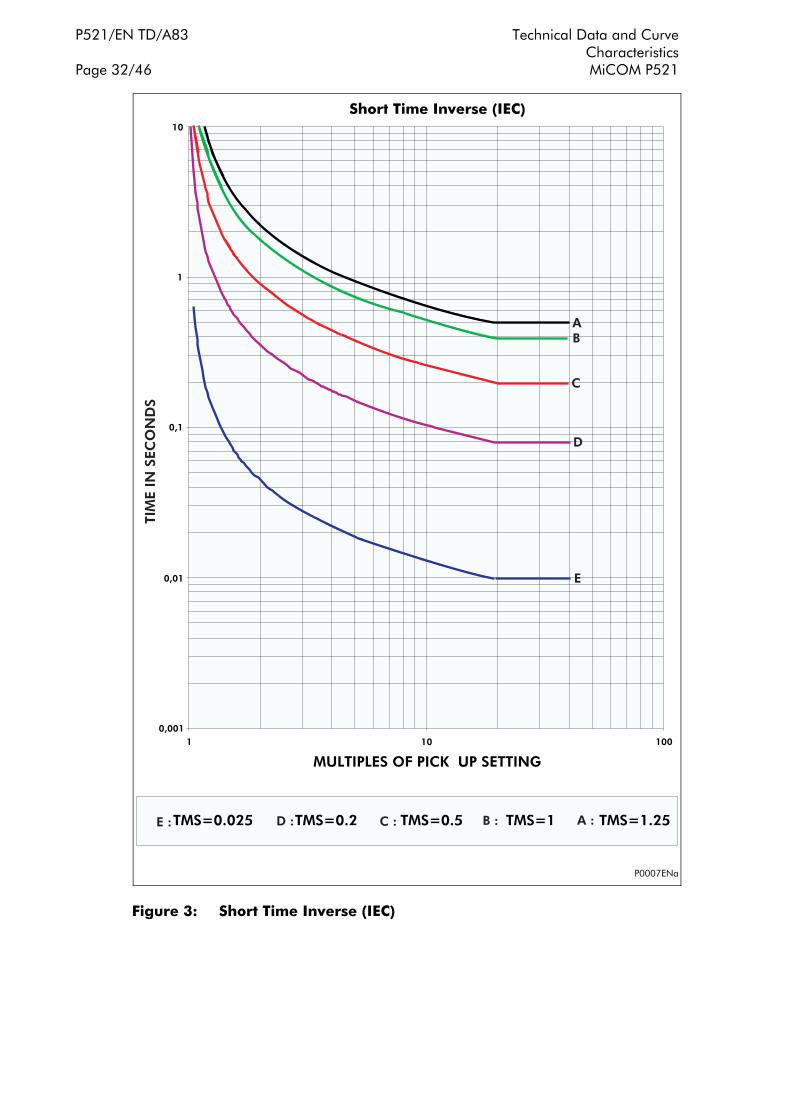
P521/EN TD/A83 Technical Data and Curve Characteristics Page 32/46 MiCOM P521
P0007ENa
Figure 3: Short Time Inverse (IEC)
Short Time Inverse (IEC)

Technical Data and Curve P521/EN TD/A83 Characteristics MiCOM P521 Page 33/46
P0008ENa
Figure 4: Standard Inverse (IEC)

P521/EN TD/A83 Technical Data and Curve Characteristics Page 34/46 MiCOM P521
P0009ENa
Figure 5: Very Inverse (IEC)
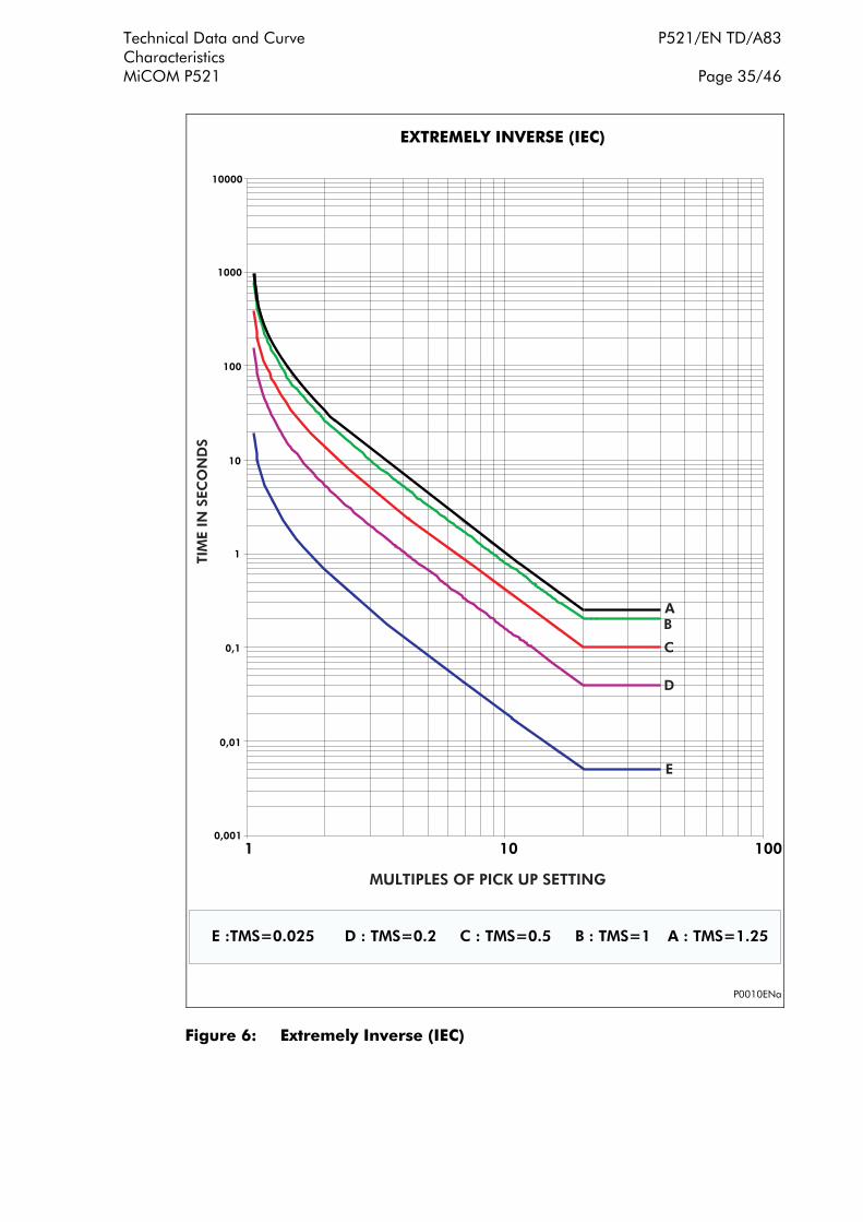
Technical Data and Curve P521/EN TD/A83 Characteristics MiCOM P521 Page 35/46
P0010ENa
Figure 6: Extremely Inverse (IEC)
EXTREMELY INVERSE (IEC)
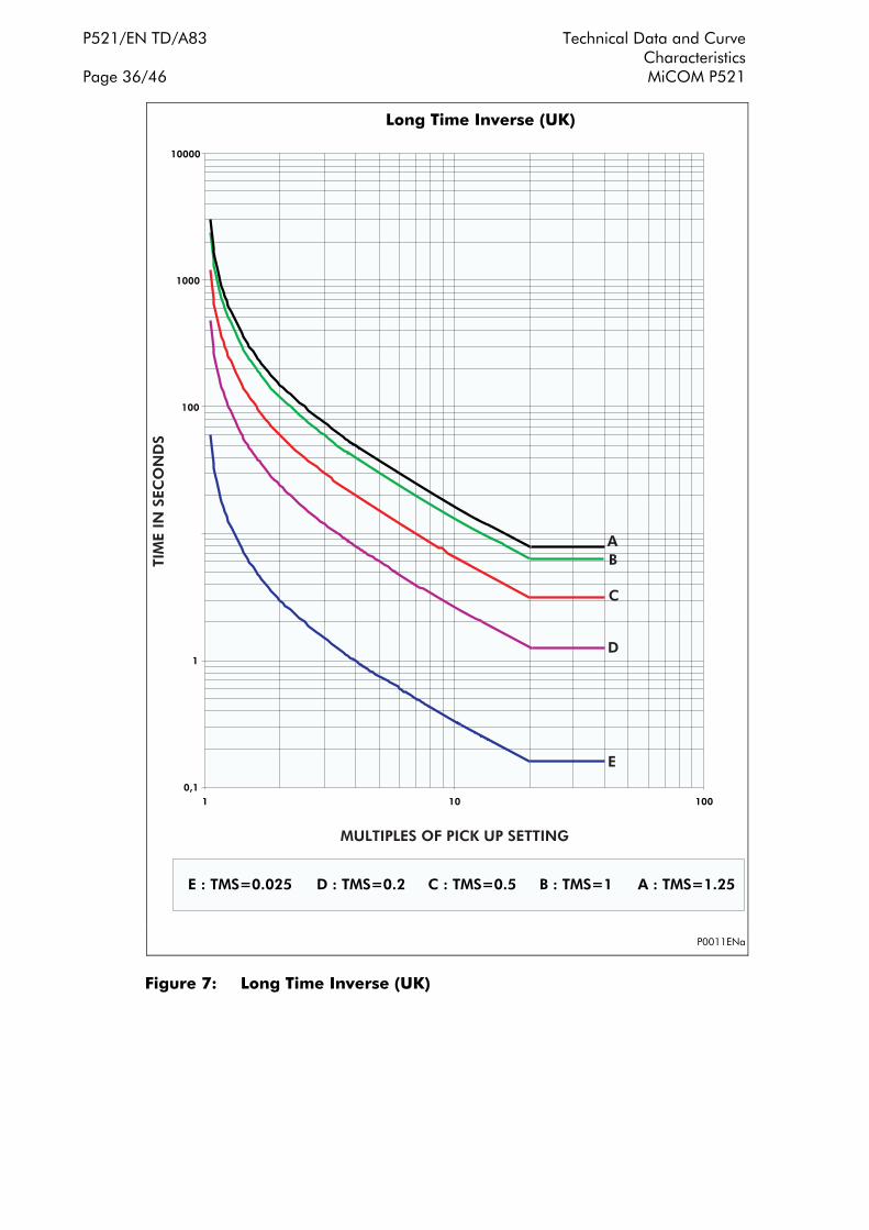
P521/EN TD/A83 Technical Data and Curve Characteristics Page 36/46 MiCOM P521
P0011ENa
Figure 7: Long Time Inverse (UK)
Long Time Inverse (UK)

Technical Data and Curve P521/EN TD/A83 Characteristics MiCOM P521 Page 37/46
17.1.4 RI curves
P0012ENa
Figure 8: RI Curves

P521/EN TD/A83 Technical Data and Curve Characteristics Page 38/46 MiCOM P521
17.1.5 IEEE/ANSI & CO curves
P0013ENa
Figure 9: ANSI/IEEE & CO curves
Short Time Inverse (CO2) Inverse (CO8) Extremely Inverse
Moderately InverseVery Inverse
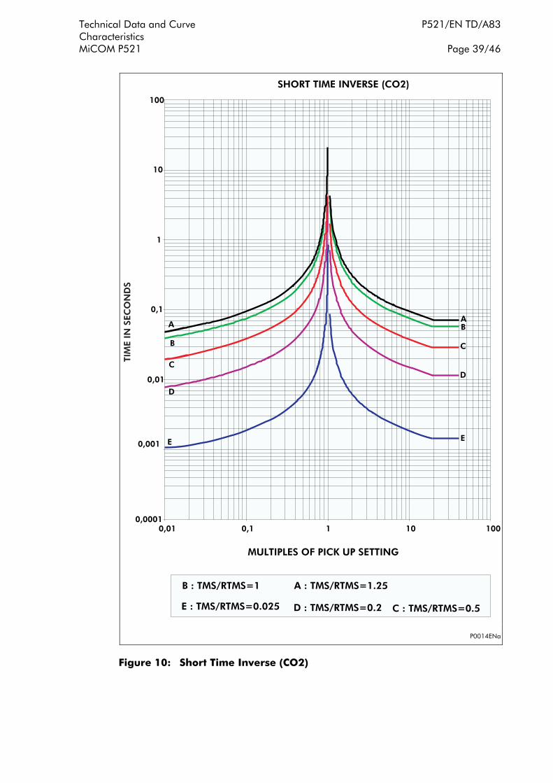
Technical Data and Curve P521/EN TD/A83 Characteristics MiCOM P521 Page 39/46
P0014ENa
Figure 10: Short Time Inverse (CO2)

P521/EN TD/A83 Technical Data and Curve Characteristics Page 40/46 MiCOM P521
P0015ENa
Figure 11: Moderately Inverse (ANSI/IEEE)

Technical Data and Curve P521/EN TD/A83 Characteristics MiCOM P521 Page 41/46
P0016ENa
Figure 12: Inverse (CO8)
TIM
E IN
SEC
ON
DS
Inverse (CO8)
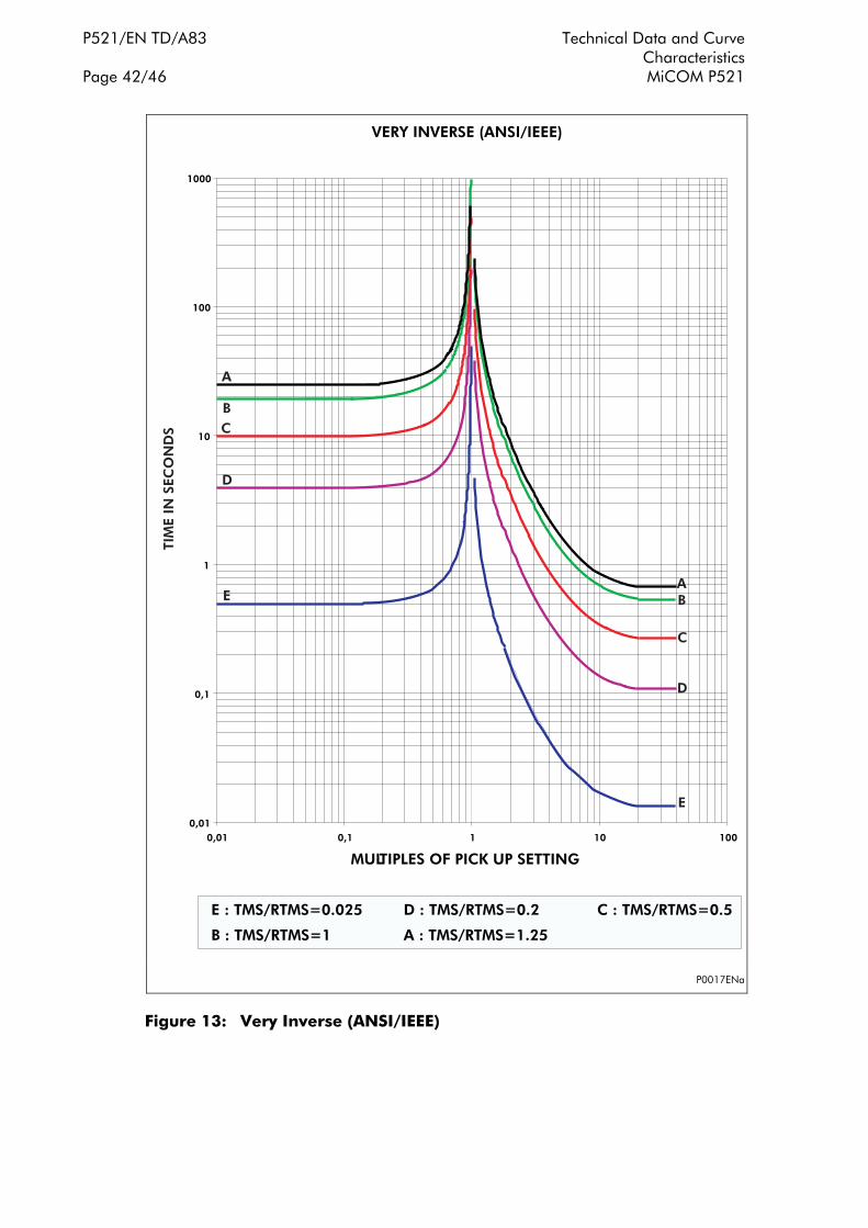
P521/EN TD/A83 Technical Data and Curve Characteristics Page 42/46 MiCOM P521
P0017ENa
Figure 13: Very Inverse (ANSI/IEEE)
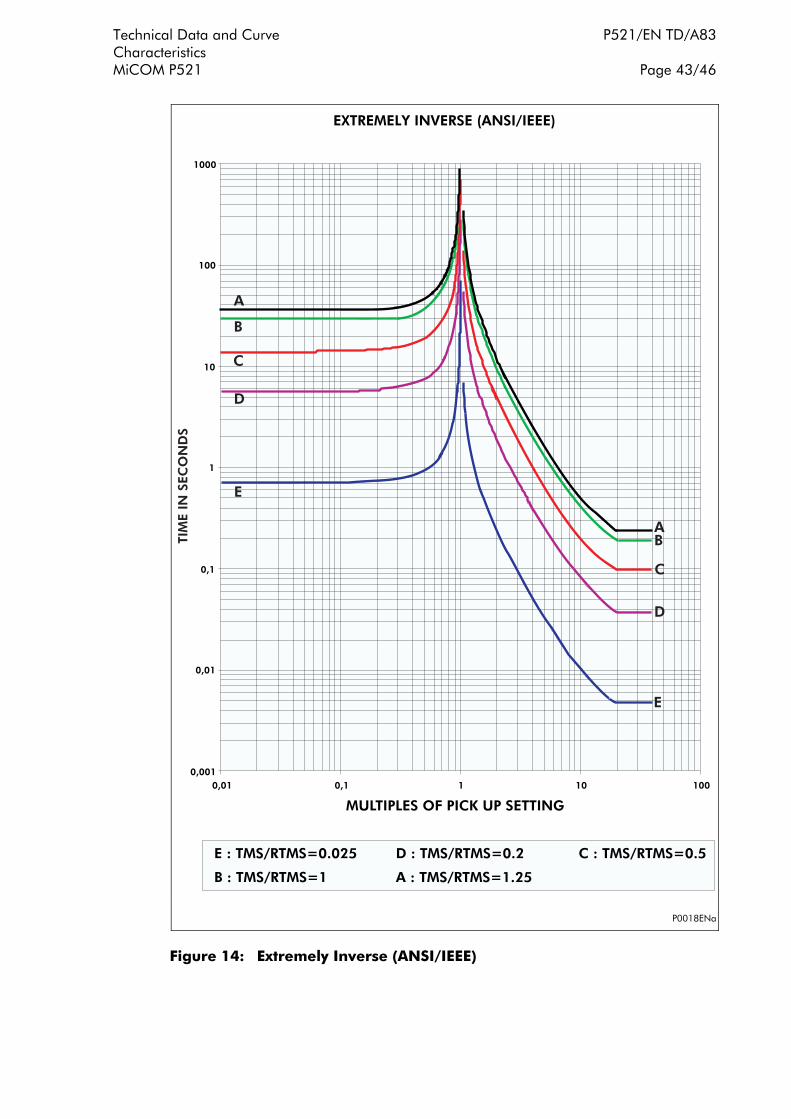
Technical Data and Curve P521/EN TD/A83 Characteristics MiCOM P521 Page 43/46
P0018ENa
Figure 14: Extremely Inverse (ANSI/IEEE)

P521/EN TD/A83 Technical Data and Curve Characteristics Page 44/46 MiCOM P521
17.1.6 Laborelec curve
Time (sec)
Prim
ary
zero
seq
uenc
e cu
rren
t (A
)
5
1.5
1.0
0.5
1
1
123
2345
1020
3040
50
P0020ENa
Figure 15: Laborele Curve

Technical Data and Curve P521/EN TD/A83 Characteristics MiCOM P521 Page 45/46
17.2 Thermal overload curves
17.2.1 Mathematical formula
The thermal time characteristic is given by:
( )( ) ⎟
⎟
⎠
⎞
⎜⎜
⎝
⎛
−
×−=⎟
⎠⎞
⎜⎝⎛ −
2
22
2
logP
FLCe II
IkItτ
Where:
t = Time to trip, following application of the overload current, Ι
τ = Heating and cooling time constant of the protected plant
Ι = Largest phase current (RMS value)
ΙFLC = Full load current rating (relay setting 'Thermal Trip')
k = 1.05 constant, allows continuous operation up to < 1.05 ΙFLC
ΙP = Steady state pre-loading before application of the overload
The time to trip varies depending on the load current carried before application of the overload, i.e. whether the overload was applied from "hot" or "cold".
Mathematical formula applicable to the MiCOM Relays:
The calculation of the time to trip is given by:
( )( )⎟
⎟⎠
⎞⎜⎜⎝
⎛
−−
=trip
eetrip IxIxxTT
θθ
2
2
log
Where:
Ttrip = Time to trip (in seconds)
Te = Thermal time constant of the protected element (in seconds)
Ix = Thermal overload equal to Ιeq, k . Ιθ >
Ιeq = Equivalent current corresponding to the RMS value of the largest phase current
Ιθ> = Full load current rating (ΙFLC) given by the national standard or by the supplier
k = Factor associated to the thermal state formula
θ2 = Initial thermal state. If the initial thermal state = 30% then
θ2 = 0.3
θtrip = Trip thermal state. If the trip thermal state is set at 100%, then θtrip = 1
The calculation of the thermal state is given by the following formula:
Erreur !
where θ is being calculated every 0.1 s.

P521/EN TD/A83 Technical Data and Curve Characteristics Page 46/46 MiCOM P521
17.2.2 Tripping curve
P0021Ena
Figure 16: Thermal Overload Tripping curve

Application Guide P521/EN AP/A83 MiCOM P521
APPLICATION GUIDE
Date: 1st October 2010
Software version: 12
Connection diagram: 10P52101

P521/EN AP/A83 Application Guide MiCOM P521

Application Guide P521/EN AP/A83 MiCOM P521 Page 1/98
CONTENTS
1. INTRODUCTION 7
1.1 P521 protection features 7
1.2 Non-protection features 8
2. APPLICATION OF INDIVIDUAL PROTECTION FUNCTIONS 9
2.1 Current differential protection 9
2.1.1 Current differential characteristics 9
2.1.2 Time alignment of current vectors 12
2.1.3 Capacitive charging current 14
2.1.4 Ratio compensation 15
2.1.5 Additional protection considerations 16
2.1.5.1 The minimum operating current 16
2.1.5.2 Relay sensitivity under heavy load conditions 16
2.1.5.3 Setting k1 less than 30% 18 2.1.6 Example settings 18
2.1.6.1 Differential element (Is1) 18
2.1.6.2 CT ratio correction 19 2.1.7 Protection of transformer feeders 20
2.1.7.1 Transformer magnetizing inrush 20
2.1.7.2 Ratio correction 24
2.1.7.3 Phase correction and zero sequence current filtering 24
2.1.7.4 Setting example of transformer feeders 26 2.1.8 In zone ‘teed’ loads 27
2.2 Overcurrent and earth fault protection 28
2.2.1 Instantaneous (start) function (50/50N) 31
2.2.2 Definite time operation (DMT) 31
2.2.3 ΙDMT thresholds 32
2.2.3.1 Inverse time curves 32 2.2.4 Laborelec curves 33
2.2.5 Reset timer 33
2.2.6 Time graded protection 35
2.3 Thermal overload protection 35

P521/EN AP/A83 Application Guide Page 2/98 MiCOM P521
2.3.1 Thermal overload characteristic 36
2.3.2 Setting guidelines 36
2.4 Circuit breaker failure protection (CBF) 38
2.4.1 Circuit breaker failure protection operation 38
2.4.2 Breaker fail timer settings 42
2.4.3 Breaker fail undercurrent settings 42
2.4.4 CBF fail logic 42
2.5 Broken conductor detection 42
2.5.1 Setting guidelines 43
2.5.2 Example setting 44
2.6 Intertripping facilities 44
2.6.1 Permissive intertrip 44
2.6.2 Direct intertrip 46
2.6.3 Programmable inter-trip 46
2.7 Negative sequence overcurrent protection 48
2.7.1 Ι2> and Ι2>> setting guidelines 49
2.8 Undercurrent protection function 50
2.9 Blocked overcurrent protection 52
2.10 Selective scheme logic 53
2.11 Cold load pick-up 54
2.11.1 Air conditioning/resistive heating loads 55
2.11.2 Motor feeders 55
2.11.3 Earth fault protection applied to transformers 56
2.11.4 Switch onto fault protection (SOTF) 56
3. APPLICATION OF NON-PROTECTION FUNCTIONS 57
3.1 Auxiliary timers (tAux 1 and tAux 2) 57
3.2 Setting group selection 57
3.2.1 Change of setting group by a logic input 58
3.2.2 Manual setting group change via front interface 58
3.3 Latch functions 58
3.4 Blocking functions 59
3.5 Circuit breaker state monitoring 60
3.6 CB control 61

Application Guide P521/EN AP/A83 MiCOM P521 Page 3/98
3.6.1 CB trip and close via user interface 61
3.6.2 CB trip and close via opto inputs 62
3.6.3 CB manual trip and close delays 62
3.7 Circuit breaker condition monitoring 62
3.7.1 Circuit breaker condition monitoring features 62
3.7.2 CB supervision settings 63
3.7.3 Setting the operating time thresholds (CB Open Time/CB Close Time) 64
3.7.4 Setting the number of operations thresholds (CB Open NB =) 64
3.7.5 Setting the Σ Ιn thresholds (Σ Amps (n)) 65
3.7.6 Setting the trip and close pulse times (t Open Pulse/t Close Pulse) 65
3.8 Trip circuit supervision 65
3.8.1 MiCOM P521 trip circuit supervision mechanism 66
3.8.2 Calculation of external resistor R1 68
3.9 Event records 69
3.10 Fault records 70
3.11 Instantaneous recorder 71
3.12 Disturbance recorder 71
3.13 Rolling and peak demand values 72
3.13.1 Rolling demand 72
3.13.2 Peak value demand 73
3.14 Measurements 73
3.14.1 Current diff 73
3.14.2 Current/general 74
3.14.2.1 Measured currents 74
3.14.2.2 Ratio of Ι2/Ι1 74
3.14.2.3 Residual harmonic currents (ΙN – fn) 74
3.14.2.4 Peak and average currents 74
3.14.2.5 Demand values 74 3.14.3 Protection comms 74
3.15 Logic Equations 75
3.16 Current transformer supervision 75
4. CURRENT TRANSFORMER REQUIREMENTS 78
4.1 Current differential protection 78

P521/EN AP/A83 Application Guide Page 4/98 MiCOM P521
4.1.1 Ks calculation 78
4.1.2 Kt calculation 78
4.2 Typical equations for current differential protection 79
4.3 Selection of X/R ratio and fault level 79
4.4 SEF protection – as fed by core-balance CT 80
5. COMMUNICATION BETWEEN RELAYS 81
5.1 Communications link options 81
5.2 Direct optical fiber 81
5.2.1 Direct optical fiber link, 850 nm multi-mode fiber 81
5.2.2 Direct optical fiber link, 1300 nm multi-mode fiber 82
5.2.3 Direct optical fiber link, 1300 nm single-mode fiber 82
5.2.4 Switched communication networks 82
5.2.5 Optical budgets 85
5.3 Multiplexer link via P59x optical fiber to electrical interface units 86
5.3.1 Multiplexer link with G.703 electrical interface using auxiliary optical fibers and type P591 interface 86
5.3.2 Multiplexer link with V.35 electrical interface using auxiliary optical fibers and type P592 interface 87
5.3.3 Multiplexer link with X.21 electrical interface using auxiliary optical fibers and type P593 interface 88
5.4 Unconditioned 4 wire pilot communications for distances greater than 1.2 km (P595) 90
5.5 Unconditioned 2 wire pilot communications for distances greater than 1.2 km91
5.5.1 Leased line modem set up (e.g. TD36 modem) 92
5.5.2 Baseband modem set up (Patton “Netlink” 1095 mDSL modem, Patton “Campus” 1092A modem) 92
5.5.3 Modem isolation 92
5.5.4 Clock source settings 92
5.6 Conditioned pilot communications 92
5.6.1 Gas discharge tubes (GDT’s) 93
5.7 Direct 4 wire EIA(RS)485 up to 1.2 km 93
5.8 Pilot isolation 94
5.9 Protection communications address 94
5.10 Clock Source 95
Application Guide P521/EN AP/A83 MiCOM P521 Page 5/98
5.10.1 Internal Clock Source signaling 95
5.10.2 External Clock Source 95
5.11 Data Rate 95
5.12 Communication failure 96
5.12.1 ‘I DIFF FAIL’ alarm 96
5.12.2 ‘COMMS ALARM CH1’ alarm 96
5.12.3 Communications failure logic 96
5.13 Communication error statistics 97
5.14 Communications delay tolerance timer 97
5.15 Communication compatibility 97
FIGURES
Figure 1 Relay bias characteristic 10
Figure 2 Propagation delay measurement 13
Figure 3 Typical plain feeder circuit 18
Figure 4 Plain feeder with unmatched CT’s 19
Figure 5 Transformer magnetizing characteristic 21
Figure 6 Magnetizing inrush waveforms 23
Figure 7 Block mode for magnetizing inrush 23
Figure 8 Need for zero-sequence current filtering 25
Figure 9 First stage phase overcurrent protection (Ι>/tΙ>) logic 29
Figure 10 Logic for overcurrent stages two, three and four 29
Figure 11 CB fail detection principle 40
Figure 12 CB open before TBF expired 40
Figure 13 CB not yet open before TBF expired 41
Figure 14 De-energization of the phase CT 41
Figure 15 Circuit breaker failure protection logic 42
Figure 16 Permissive intertrip 45
Figure 17 Direct intertrip 46
Figure 18 Digital signal transfer 47
Figure 19 Undercurrent protection logic 50
Figure 20 Blocked overcurrent scheme 52
Figure 21 Typical scheme logic 53
Figure 22 Blocking logic for selected protection features 60
Figure 23 CB Status DBI logic diagram 61
P521/EN AP/A83 Application Guide Page 6/98 MiCOM P521
Figure 24 Trip circuit supervision logic diagram 66
Figure 25 Trip coil monitoring 67
Figure 26 Trip coil and auxiliary contact monitoring 67
Figure 27 Trip coil and auxiliary contact monitoring regardless of CB position 68
Figure 28 Example of logic equation 75
Figure 29 Current transformer supervision 76
Figure 30 Switched communication network 84
Figure 31 Modified bias characteristic 84
Figure 32 MT-RS485 connection diagram 93
Figure 33 Communications failure logic 96

Application Guide P521/EN AP/A83 MiCOM P521 Page 7/98
1. INTRODUCTION
The MiCOM P521 relay has been designed to provide more functionality in terms of protection, measuring, automatic operation and control in any low/medium voltage electrical network.
These relays can be used at industrial and distribution levels to overcome grading difficulties in complex networks. For distribution systems, continuity of supply is of paramount importance. Faults within the protected zone will be cleared very quickly by the MiCOM P521, therefore minimizing damage and disruption to the rest of the system. The majority of overhead line faults are semi-permanent in nature. Multi-shot auto-reclose can therefore be used in conjunction with the P521 once again minimizing disruption to the system. The relay also has various other protection features such as overcurrent and earth fault protection. These features can be either permanently enabled or enabled when the differential communication channel fails. The phase and earth fault protection have four stages that can be set either instantaneous or ΙDMT (stages 1 and 2 only). There is also a wide choice of operating time curves (ΙEC, UK, ANSI/IEEE, C0, LABORELEC and Rectifier) which makes it possible to adapt these relays to an existing protection scheme, irrespective of the other relays already installed on the network.
A choice of protection communications mediums are also available; these include electrical (i.e. pilot wires etc.), modem communications, multiplexed networks and direct fiber optic links.
The P521 also offers the ability to change the protection communications interface from electrical to fiber optic without the need for a software/firmware upgrade. This allows the P521 to be applied to networks that are to have their protection communication upgraded in the future.
1.1 P521 protection features
The P521 has the following protection features:
− Phase current differential protection [87] - Phase segregated biased differential protection provides the main protection element for the relay. Provides high speed, discriminative protection for all fault types. Provides differential protection for the feeders with transformer in-zone.
− Phase fault overcurrent protection [50/51] - Four stage time delayed or instantaneous backup protection.
− Earth fault protection [50N/51N] - Four stage backup time delayed or instantaneous protection. (Normal, sensitive and very sensitive earth fault ranges are available at the ordering stage).
− True RMS thermal protection [49] - Thermal protection for overhead lines and cables.
− Undercurrent protection [37] - To detect loss of load conditions.
− Broken conductor protection - To detect open circuit faults
− Negative sequence overcurrent protection [46] - This can be selected to provide remote backup protection for phase to phase or phase to earth faults.
− Circuit breaker fail protection - To take remedial action in the event of slow or inoperable circuit breaker.
− Trip circuit supervision - Checks the integrity of the trip circuit and the trip circuit supply voltage. In the event that the trip circuit becomes open circuit, or the trip circuit supply voltage is lost, the relay will issue a trip circuit fail alarm.

P521/EN AP/A83 Application Guide Page 8/98 MiCOM P521
− Direct/permissive intertrip - Independent intertripping facility using the relay's protection communications channels.
− Programmable inter-trip commands – Four independent inter-trip commands are provided in addition to the Direct/permissive inter-trips. Protection, binary input and logic equation signals can be assigned to initiate an inter-trip.
− Protection communications supervision - To detect failure of protection communications and enable remedial action to be taken, i.e. switch in communication independent backup protections (e.g. overcurrent and earth fault protection).
− Cold load pick-up logic - May be used to transiently raise the setting for both the phase and the earth fault protection.
− Selective overcurrent logic - Provides the capability of temporarily altering the time settings of stages 2, 3 and 4 of the phase overcurrent and earth fault elements.
− CTS – Current transformer supervision can detect CT failures and prevent differential, negative sequence overcurrent and undercurrent protection from mal-operation.
1.2 Non-protection features
Below is a summary of the P521 relay non-protection features.
− Local/remote measurements - Various measurement values from the local and remote line ends available for display on the relay or accessed from the serial communications.
− Front EIA(RS)232 communication port (MODBUS only).
− Rear EIA(RS)485 communication port - Provides remote serial communications. The following communications protocols are supported: MODBUS, IEC 60870-5-103, DNP3.0.
− Fault/event/disturbance records - Available from the serial communications or on the relay LCD (fault and event records only).
− Two setting groups - Independent setting groups to cater for switched feeding or customer specific applications.
− Selectable phase rotation.
− Circuit breaker control - Control of the circuit breaker can be achieved either locally via the user interface or remotely.
− Circuit breaker condition monitoring - Provides records/alarm outputs regarding the number of CB operations, cumulative interruption duty, and the breaker operating/closing time.
− Commissioning test facilities - Allows the user to test the LEDs, energize selected output relays, freeze circuit breaker measurements and enable LOOPBACK mode.
− Continuous self-monitoring - Power on diagnostics and self checking routines to provide maximum relay reliability and availability.
− Logic equations – Eight Boolean logic equations are available, each with maximum 16 variants, which can be chosen from signals of protection, binary input, alarm and output of other logic equations.

Application Guide P521/EN AP/A83 MiCOM P521 Page 9/98
2. APPLICATION OF INDIVIDUAL PROTECTION FUNCTIONS
The following sections detail the individual protection functions in addition to where and how they may be applied. Each section also gives an extract from the respective menu columns to demonstrate how the settings are actually applied to the relay.
2.1 Current differential protection
The primary protection element of the P521 relay is the current differential protection. This technique involves the comparison of the currents at each end of the line. A communications path is therefore an essential requirement of any such scheme. The P521 relay utilizes a 9.6/19.2/56/64 kbits/s digital communications system either for direct optical fiber between ends, direct EIA(RS)485 link, modem connections, or via a multiplexed link.
2.1.1 Current differential characteristics
The basic operating principle of differential protection is to calculate the difference between the currents entering and leaving a protected zone. The protection operates when this difference exceeds a set threshold.
Differential currents may also be generated during external fault conditions due to CT saturation. To provide stability for through fault conditions, the relay adopts a biasing technique. This method effectively raises the setting of the relay in proportion to the value of through fault current to prevent relay maloperation. Figure 1 shows the operating characteristics of the P521 phase differential element.
The differential current is calculated as the vector summation of the currents entering the protected zone. The bias current is the average of the measured current at each line end. It is found by the scalar sum of the current at each terminal, divided by two. Both of these calculations are based upon the fundamental component of the line currents only.
Each of these calculations is done on a phase by phase basis. The level of bias used for each element is the highest of the three calculated for optimum stability.

P521/EN AP/A83 Application Guide Page 10/98 MiCOM P521
Figure 1 Relay bias characteristic
The characteristic is determined by four protection settings:
Ιs1 The basic differential current setting which determines the minimum pick-up level of the relay.
k1 The lower percentage bias setting used when the bias current is below
Ιs2. This provides stability for small CT mismatches, whilst ensuring good sensitivity to resistive faults under heavy load conditions.
Ιs2 A bias current threshold setting, above which the higher percentage bias k2 is used.
k2 The higher percentage bias setting used to improve relay stability under heavy through fault current conditions.
The tripping criteria can be formulated as:
1. for |Ιbias| < Ιs2,
|Ιdiff| > k1.| Ιbias| + Ιs1
2. for |Ιbias| > Ιs2,
|Ιdiff| > k2.| Ιbias| - (k2 - k1). Ιs2 + Ιs1
When a trip is issued by the differential element, in addition to tripping the local breaker, the relay will send a differential intertrip signal to the remote relay. This will ensure tripping of both ends of the protected line, even for marginal fault conditions. The relay receiving the intertrip signal will indicate that it has operated due to a differential intertrip by displaying “Ι DIFF Ι-TRIP”.
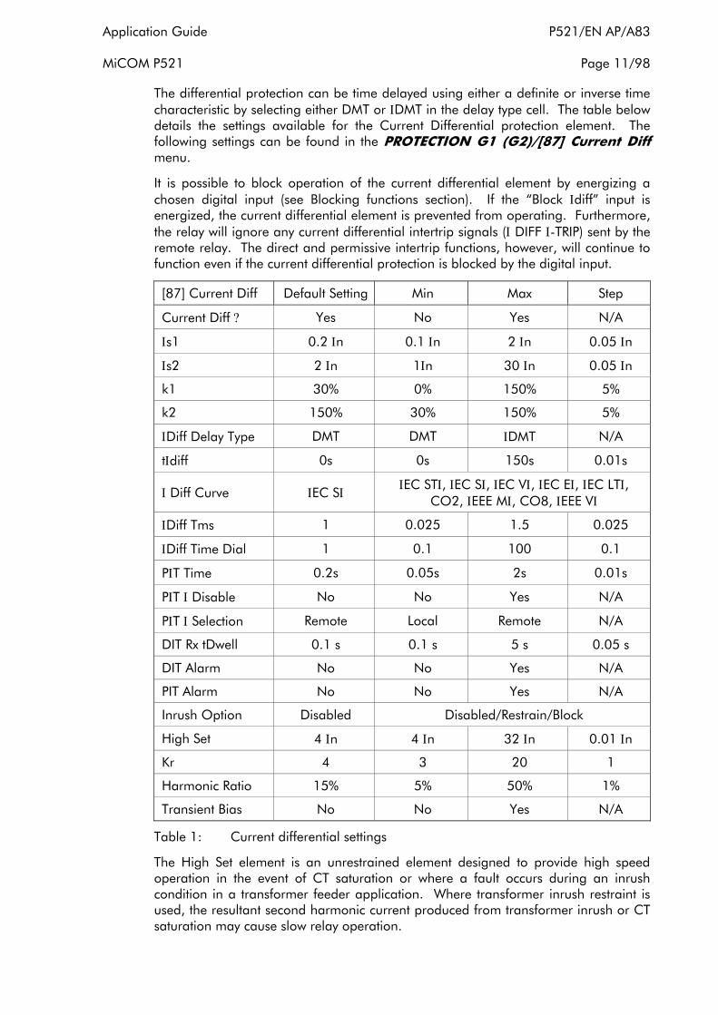
Application Guide P521/EN AP/A83 MiCOM P521 Page 11/98
The differential protection can be time delayed using either a definite or inverse time characteristic by selecting either DMT or ΙDMT in the delay type cell. The table below details the settings available for the Current Differential protection element. The following settings can be found in the PROTECTION G1 (G2)/[87] Current Diff menu.
It is possible to block operation of the current differential element by energizing a chosen digital input (see Blocking functions section). If the “Block Ιdiff” input is energized, the current differential element is prevented from operating. Furthermore, the relay will ignore any current differential intertrip signals (Ι DIFF Ι-TRIP) sent by the remote relay. The direct and permissive intertrip functions, however, will continue to function even if the current differential protection is blocked by the digital input.
[87] Current Diff Default Setting Min Max Step
Current Diff ? Yes No Yes N/A
Ιs1 0.2 Ιn 0.1 Ιn 2 Ιn 0.05 Ιn
Ιs2 2 Ιn 1Ιn 30 Ιn 0.05 Ιn
k1 30% 0% 150% 5%
k2 150% 30% 150% 5%
ΙDiff Delay Type DMT DMT ΙDMT N/A
tΙdiff 0s 0s 150s 0.01s
Ι Diff Curve ΙEC SΙ ΙEC STΙ, ΙEC SΙ, ΙEC VΙ, ΙEC EΙ, ΙEC LTΙ,
CO2, ΙEEE MΙ, CO8, ΙEEE VΙ
ΙDiff Tms 1 0.025 1.5 0.025
ΙDiff Time Dial 1 0.1 100 0.1
PΙT Time 0.2s 0.05s 2s 0.01s
PΙT Ι Disable No No Yes N/A
PΙT Ι Selection Remote Local Remote N/A
DIT Rx tDwell 0.1 s 0.1 s 5 s 0.05 s
DIT Alarm No No Yes N/A
PIT Alarm No No Yes N/A
Inrush Option Disabled Disabled/Restrain/Block
High Set 4 Ιn 4 Ιn 32 Ιn 0.01 Ιn
Kr 4 3 20 1
Harmonic Ratio 15% 5% 50% 1%
Transient Bias No No Yes N/A
Table 1: Current differential settings
The High Set element is an unrestrained element designed to provide high speed operation in the event of CT saturation or where a fault occurs during an inrush condition in a transformer feeder application. Where transformer inrush restraint is used, the resultant second harmonic current produced from transformer inrush or CT saturation may cause slow relay operation.

P521/EN AP/A83 Application Guide Page 12/98 MiCOM P521
The High Set element is only visible and activated when Inrush Restraint is enabled, to overcome this condition. The High Set element should be set in excess of 40% of the peak magnetizing inrush current.
Transient Bias is a new feature that increases relay stability during local-end primary CT saturation under external fault conditions.
When CT saturation occurs, the waveforms sampled by the relay can become distorted, leading to unwanted differential currents. The CT saturation will normally dissipate over time, so it is transient in nature.
It is not necessary for differential protection to be blocked when CT saturation is detected - the P521 ensures stability under this condition by temporarily raising the differential current characteristic threshold by applying an additional bias component.
This additional bias component is allowed to decay to ensure it is transient in nature and mimics the behavior of the CT saturation. As a result the relay is able to withstand larger amounts of CT saturation without tripping. The Transient Bias function can be used to mitigate transient CT saturation only, as sustained saturation will remain after the decay has elapsed.
2.1.2 Time alignment of current vectors
To calculate differential current between line ends it is necessary that the current samples from each end are taken at the same moment in time. This can be achieved by time synchronizing the sampling, or alternatively, by the continuous calculation of the propagation delay between line ends. The P521 relay has adopted this second technique.
Consider the two-ended system as shown in Figure 2.
Two identical relays, A and B are placed at the two ends of the line. Relay A samples its current signals at time tA1, tA2 etc., and relay B at time tB1, tB2 etc.
Note: The sampling instants at the two ends will not, in general, be coincidental or of a fixed relationship, due to slight drifts in sampling frequencies.

Application Guide P521/EN AP/A83 MiCOM P521 Page 13/98
!""#!
$#" "%&'
!! (")%&&'
*#+!
, & " ! (, & " ! ( & !! ("!" (! & !! ("!" (! & "-.+ !"
(.!" & + "!" ( & + "!" ( & ."#" "!( (
*#+!
Figure 2 Propagation delay measurement
Assume that at time tA1, relay A sends a data message to relay B. The message contains a time tag, tA1, together with other timing and status information and the current vector values calculated at tA1. The message arrives at end B after a channel propagation delay time, tp1. Relay B registers the arrival time of the message as tB*.
Since relays A and B are identical, relay B also sends out data messages to end A. Assume relay B sends out a data message at tB3. The message therefore contains the time tag tB3. It also returns the last received time tag from relay A (i.e. tA1) and the delay time, td, between the arrival time of the received message, tB*, and the sampling time, tB3, i.e. td = (tB3 - tB*).
The message arrives at end A after a channel propagation delay time, tp2. Its arrival time is registered by relay A as tA*. From the returned time tag, tA1, relay A can measure the total elapsed time as (tA* - tA1). This equals the sum of the propagation delay times tp1, tp2 and the delay time td at end B.
Hence,
(tA* - tA1) = (td + tp1 + tp2)
The relay assumes the transmit and receive channels follow the same path so they have the same propagation delay time. This time is calculated as follows:
tp1 = tp2 = ½ (tA* - tA1 - td)

P521/EN AP/A83 Application Guide Page 14/98 MiCOM P521
Note: The propagation delay time is measured for each received sample and this can be used to monitor any change on the communication link.
As the propagation delay time has now been deduced, the sampling instant of the received data from relay B (tB3*) can be calculated. As shown in Figure 2, the sampling time tB3* is measured by relay A as:
tB3* = (tA* - tp2)
In Figure 2, tB3* is between tA3 and tA4. To calculate the differential and bias currents, the vector samples at each line end must correspond to the same point in time. It is necessary therefore to time align the received tB3* data to tA3 and tA4. This can be achieved by rotating the received current vector by an angle corresponding to the time difference between tB3* and tA3 (and tA4). For example a time difference of 1ms would require a vector rotation of 1/
20 * 360° = 18° for a 50Hz system.
As two data samples can be compared with each data message, this process will have the effect of increasing the operating speed for any given bandwidth.
Note: The current vectors of the three phases need to be time aligned separately.
2.1.3 Capacitive charging current
The charging current of a line or cable will be seen as differential current. If this current is of a sufficiently high magnitude, as is the case for cables and long feeders, then relay maloperation could occur. Two issues are apparent with charging current; the first being inrush during line energization and the second being steady state charging current.
Inrush charging current is normally a high order harmonic (9th or 11th for example). The Fourier filtering used by the P521 relay will remove these frequency components and hence provide stability.
Steady state charging current is nominally at fundamental frequency and hence may cause relay maloperation.
To overcome this problem it must be ensured that the base current setting on the relay (Ιs1) is set to at least 2.5x the steady state line charging current to avoid possible maloperation.
The table below shows some typical steady state charging currents for various lines and cables.
Voltage (kV) Core Formation and
Spacing Conductor Size
in mm2 Charging
Current A/km
11 kV Cable Three-core 120 1.2
33 kV Cable Three-core 120 1.8
33 kV Cable Close-trefoil 300 2.5
66 kV Cable Flat, 127 mm 630 10
132 kV Overhead Line - 175 0.22
132 kV Overhead Line - 400 0.44
132 kV Cable Three-core 500 10
132 kV Cable Flat, 520 mm 600 20

Application Guide P521/EN AP/A83 MiCOM P521 Page 15/98
Voltage (kV) Core Formation and
Spacing Conductor Size
in mm2 Charging
Current A/km
275 kV Overhead Line - 2 x 175 0.58
275 kV Overhead Line - 2 x 400 0.58
275 kV Cable Flat, 205 mm 1150 19
275 kV Cable Flat, 260 mm 2000 24
400 kV Overhead Line - 2 x 400 0.85
400 kV Overhead Line - 4 x 400 0.98
400 kV Cable Flat, 145 mm 2000 28
400 kV Cable Tref., 585 mm 3000 33
Table 2: Typical cable/line charging currents (UK, 50 Hz)
2.1.4 Ratio compensation
To ensure correct operation of the differential element, it is important that under load and through fault conditions, the currents into the differential element of the relay are balanced. In some cases, the current transformer primary ratings at each end of the line will not exactly match. A ratio correction factor (CONFIGURATION/CT Ratio/CT Correct Ratio) is therefore provided which is adjustable from 0.05 to 2 in steps of 0.01. The CT ratio correction factor is applied to ensure that the signals to the differential algorithm are correct.
Ideally, the compensated current values should be arranged to be as close as possible to the relay rated current to provide optimum relay sensitivity. The corrected currents should not, however, be arranged to exceed relay rated current under through load conditions.
In general, CT Correction Ration can be calculated as below.
For end each end a and b, their Correction Ration ka and kb can be defined as:
aref
ana I
Ik
,
,=
bref
bnb I
Ik
,
,=
Where,
In,a Rated current of CT primary at end a
In,b Rated current of CT primary at end b
Iref,a Reference current of end a
Iref,b Reference current of end b
Reference currents are determined as follows:
an
refaref V
SI
,, 3
=

P521/EN AP/A83 Application Guide Page 16/98 MiCOM P521
bn
refbref V
SI
,, 3
=
Where
Sref Reference power. For feeder application, it can be determined by rated current multiplying rated voltage. Alternatively, use the rated current of the feeder as Iref. For transformer application, the rated power of the transformer can be used.
Note 1: CT rated current In and reference current Iref in above calculation are all in primary values. Secondary values can also be used in calculation, see section 2.1.6.2 as an example.
Note 2: Since software version V12.A, the upper range of CT correction factor is increased from 2 to 10. This allows proper setting of this factor for the situation where the primary rating current of a CT is too higher than the actual rating current.
2.1.5 Additional protection considerations
2.1.5.1 The minimum operating current
Note: The minimum operating current is related, but not equal to, the Is1 setting.
Consider a single end fed fault with no load but fault current, I:
|Ιdiff| = Ι |Ιbias|= ½Ι
Assuming |Ιbias| < Ιs2, then, using the equation 1 from section 2.1.1, the relay will operate if:
|Ιdiff| > k1.| Ιbias| + Ιs1 or Ι > k1.½Ι + Ιs1 or Ι > Ιs1 / (1 - 0.5 k1)
The minimum operating current is therefore a function of the Ιs1 and k1 settings. Since k1 is recommended to be set to 30%, the minimum operating current will be:
Ιmin = 1.176 Ιs1
For most applications a minimum setting of 0.2 pu is recommended. This will give the relay a sensitivity of 0.235 pu.
2.1.5.2 Relay sensitivity under heavy load conditions
The sensitivity of the relay is governed by its settings and also the magnitude of load current in the system. For a two-ended system, with relays X and Y, the following applies:
|Ιdiff| = |(ΙX + ΙY)|
|Ιbias| = 0.5 (|ΙX| + |ΙY|)
Assume a load current of ΙL flowing from end X to Y. Assume also a high resistance fault of current ΙF being singly fed from end X. For worst case analysis, we can assume also ΙF to be in phase with ΙL:
ΙX = ΙL + ΙF

Application Guide P521/EN AP/A83 MiCOM P521 Page 17/98
ΙY = ΙL
|Ιdiff| = |ΙF|
|Ιbias| = |ΙL| + 0.5 |ΙF|
Relay sensitivity when |Ιbias| < Ιs2:
For |Ιbias| < Ιs2, the relay would operate if |Ιdiff| > k1 |Ιbias| + Ιs1
or |ΙF| > k1 (|ΙL| + 0.5 |ΙF|) + Ιs1
or (1 - 0.5 k1) |ΙF| > (k1 |ΙL| + Ιs1)
or |ΙF| > (k1 |ΙL| + Ιs1) / (1 - 0.5 k1)
For Ιs1 = 0.2 pu, k1 = 30% and Ιs2 =2.0 pu, then
1. for |ΙL| = 1.0 pu, the relay would operate if |ΙF| > 0.59 pu
2. for |ΙL| = 1.59 pu, the relay would operate if |ΙF| > 0.80 pu
If |ΙF| = 0.80 pu and |ΙF| = 1.59 pu, then |Ιbias| = 1.99 pu which reaches the limit of the low percentage bias curve.
Relay sensitivity when |Ιbias| > Is2:
For |Ιbias| > Ιs2, the relay would operate if
|Ιdiff| > k2 |Ιbias| - (k2 - k1) Ιs2 + Ιs1
or |ΙF| > k2 (|ΙL| + 0.5 |ΙF|) - (k2 - k1) Ιs2 + Ιs1
or (1 - 0.5 k2) |ΙF| > (k2 |ΙL| - (k2 - k1) Ιs2 + Ιs1)
or |ΙF| > (k2 |ΙL| - (k2 - k1) Ιs2 + Ιs1) / (1 - 0.5 k2)
For Ιs1 = 0.2 pu, k1 = 30%, Ιs2 = 2.0 pu and k2 = 100%, then,
3. for |ΙL| = 2.0 pu, the relay would operate if |ΙF| > 1.6 pu
4. for |ΙL| = 2.5 pu, the relay would operate if |ΙF| > 2.6 pu
Fault resistance coverage:
Assuming the fault resistance, RF, is much higher than the line impedance and source impedance, then for a 33kV system and 400/1 CT:
|ΙF| = ( Vph-n /RF ) * ( 1/CT ratio) pu
= ((33000 / 3 ) / RF) / 400 pu
= 47.63/RF pu
Based on the above analysis, the relay will detect a fault current in excess of 0.59 pu with a load current of 1 pu flowing. The fault resistance would have to be less than 47.63/0.59 = 81Ω in this case.
With a short time overload current of 2.0 pu, the relay will be able to detect a fault resistance of 47.63/1.6 = 30 Ω or lower.

P521/EN AP/A83 Application Guide Page 18/98 MiCOM P521
2.1.5.3 Setting k1 less than 30%
If desired, k1 can be set to less than the recommended setting of 30%, down to a minimum of 0%, to increase relay sensitivity. However, if doing so the user should consult Schneider Electric T&D concerning the CT requirements. This is because under certain conditions on systems with high X/R ratio and low fault currents there may be stability issues with a very low k1 setting.
2.1.6 Example settings
2.1.6.1 Differential element (Is1)
All four settings are user adjustable. This flexibility in settings allows the relay characteristic to be tailored to suit a particular sensitivity and CT requirements. To simplify the protection engineer’s task, we strongly recommend three of the settings be fixed to:
Ιs2 = 2.0 pu k1 = 30% k2 = 150%
These settings will give a relay characteristic suitable for most applications. It leaves only the Is1 setting to be decided by the user. The value of this setting should be in excess of any mismatch between line ends although the CT ratio correction factor can be used to alleviate this problem. The effects of capacitive line charging current, if any, must also be considered when deciding the Ιs1 setting.
By considering the circuit shown in Figure 3, the settings for the current differential element can be established.
!"# !"$
Figure 3 Typical plain feeder circuit
The following settings should be set as follows:
Ιs2 = 2.0 pu
k1 = 30 %
k2 = 150 % (for a two terminal application)
This leaves the setting of Ιs1 to be established.

Application Guide P521/EN AP/A83 MiCOM P521 Page 19/98
The Is1 setting for the P521 relay must be set above 2.5 times the steady state line charging current value. In this example, assume a cable is used:
Ιs1 > 2.5 x Ιch
Ιs1 > 2.5 x (25 km x 2.5 A/km)
Ιs1 > 156.25 A
The line CTs are rated at 400 amps primary. The setting of Ιs1 must therefore exceed 156.25/400 = 0.391 pu.
Therefore select:
Ιs1 = 0.4 pu
2.1.6.2 CT ratio correction
In cases where different CT ratios are used at each line end the relay can be set with a CT ratio correction factor “CT Correct Ratio” (CONFIGURATION/CT Ratio). Assuming the relay is applied to the system shown in Figure 4 and the maximum full load current was 375 Amps the relay can be set as follows.
/
( (
400) 0)
/
035 304
!""#!
Figure 4 Plain feeder with unmatched CT’s
It is good practice to correct the mismatched current to rated current to maintain good sensitivity for high resistance faults. In this example the current entering relay 1 must be scaled upwards, whereas the current entering relay 2 must be scaled down.
To calculate the correction factor for relay 1:
Current entering relay 1 = 375 / 400 = 0.938 A
To correct to rated current our correction factor must be 1/0.938 = 1.071
The same can be done for relay 2.
To calculate the correction factor for relay 2:
Current entering relay 1 = 375 / 350 = 1.071 A
To correct to rated current our correction factor must be 1/1.071 = 0.938
The differential spill current will now be reduced to practically zero instead of 0.133 A (1.071-0.938) which was the current before the any correction.

P521/EN AP/A83 Application Guide Page 20/98 MiCOM P521
2.1.7 Protection of transformer feeders
In applying the well established principles of differential protection to transformers, a variety of considerations have to be taken into account. These include compensation for any phase shift across the transformer, possible unbalance of signals from current transformers either side of windings, and the effects of the variety of earthing and winding arrangements. In addition to these factors, which can be compensated for by correct application of the relay, the effects of normal system conditions on relay operation must also be considered. The differential element must restrain for system conditions which could result in maloperation of the relay, such as high levels of magnetizing current during inrush conditions.
In traditional transformer feeder differential schemes, the requirements for phase and ratio compensation were met by correct selection of the line current transformers. The P521 (from software version 2.A) provides software interposing current transformers (ICTs) to give the required vector compensation. The advantage of having replica ICTs is that they give the P521 relays the flexibility to cater for line CTs connected in either star or delta, as well as being able to compensate for a variety of system earthing arrangements.
A further consideration is the operation of differential protection for faults during transformer inrush conditions. An unrestrained differential High Set element is provided to ensure high speed operation under these conditions, as well as in the event of CT saturation, which produces second harmonics.
Ratio compensation, however, is provided by adjusting a software CT ratio correction factor (see section 2.1.6.2).
2.1.7.1 Transformer magnetizing inrush
The magnetizing inrush current to a transformer appears as a large operating signal to the differential protection. Special measures are taken with the relay design to ensure that no maloperation occurs during inrush.
Figure 5 shows a transformer magnetizing characteristic. To minimize material costs, weight and size, transformers are generally operated near to the ‘knee point’ of the magnetizing characteristic. Consequently, only a small increase in core flux above normal operating levels will result in a high magnetizing current.

Application Guide P521/EN AP/A83 MiCOM P521 Page 21/98
Figure 5 Transformer magnetizing characteristic
Under normal steady state conditions, the magnetizing current associated with the operating flux level is relatively small (usually less than 1% of rated current). However, if a transformer winding is energized at a voltage zero, with no remnant flux, the flux level during the first voltage cycle (2 x normal max. flux) will result in core saturation and in a high, non-sinusoidal magnetizing current waveform. This current is commonly referred to as magnetizing inrush current and may persist for several cycles. The magnitude and duration of magnetizing inrush current waveforms are dependent upon a number of factors, such as transformer design, size, system fault level, point on wave of switching, number of banked transformers, etc. Figure 6 shows typical transformer magnetizing currents for steady state and inrush conditions.
The magnetizing inrush current contains a high percentage of second harmonic. The MiCOM P521 relay filters out this component of the waveform and makes use of it to achieve stability. There are two options available, Restrain and Block. To enable the inrush option facility the user can select from the menu cell PROTECTION G1 (G2)/[87] Current Diff/ Inrush Option.
Restrain mode:
In this mode, the relay uses the second harmonic component as an additional bias quantity. The total bias used by the relay will therefore be a combination of the average load current on the line plus a multiple of the second harmonic component of the current. The multiplying factor used to ensure stability is set by Kr.
Kr is a setting that allows compensation for the effects of 2nd harmonic and CT ratio correction on the bias current. When set correctly it will ensure stability under magnetising inrush conditions. Kr is described by the following equations, and it is our recommendation that it is set taking into account the level of 2nd harmonic likely to be generated by the transformer under typical inrush conditions. Section 2.1.7.4 gives an example of calcuation of Kr.
P521/EN AP/A83 Application Guide Page 22/98 MiCOM P521
The additional bias is calculated by:
2_ IhKrI biasadditional ×=
Now the tripping criteria can be formulated as:
For ( )( ) 222/ IsIhKrIremIloc ≤×++ ,
( )( )22/11 IhKrIremIlockIsIdiff ×++×+>
For ( )( ) 222/ IsIhKrIremIloc >×++ ,
( )( ) ( ) 21222/21 IskkIhKrIremIlockIsIdiff ×−−×++×+>
The value of Ih2 used above is the maximum second harmonic in three phases, obtained from both local and remote ends.
As Kr directly affects the bias curve, it should be noted that it operates as a restrain function, and in the absence of any information on 2nd harmonic content, setting Kr too high to ensure stability may result in longer operating times for internal faults currents below the high set value.
Block mode:
For any of the three phases, if the level of phase current is above 5% In, and if the ratio of Ih2 to fundamental in the line is above the Harmonic Ratio setting, the differential protection will be blocked at both local and remote end, unless the differential current is larger than the high set value. (refer to Figure 7).
Note1: If block mode is required, it should be set at both ends. If block mode is set at only one end, an alarm “Conf. Alarm Inrush” will be generated on the front panel LCD at both end relays. The relay that is not set in block mode will not be blocked by the local nor remote end inrush current.
Note2: To work in Block mode, the relays must be set in Extension communication mode in the menu COMMUNICATION/Protection/FRAME MODE.

Application Guide P521/EN AP/A83 MiCOM P521 Page 23/98
/"
&"
"
/
2(
2-.!+! 6!
Figure 6 Magnetizing inrush waveforms
IAIh2/Ih1 > Setting
&
ICIh2/Ih1 > Setting
IBIh2/Ih1 > Setting
Set: 2nd Harmonic
Disabled
Restraint
Blocking
&
&
Idiff no trip 1Intsig: Ih(2) Local Inrush Blk
1Intsig: Ih(2) Block AIntsig: Ih(2) Block BIntsig: Ih(2) Block C
*
*
* *
Intsig received in message
Intsig sent in message
Intsig: Ih(2) Rem Inrush Blk
Reserved
Reserved
Reserved
Figure 7 Block mode for magnetizing inrush

P521/EN AP/A83 Application Guide Page 24/98 MiCOM P521
2.1.7.2 Ratio correction
To ensure correct operation of the differential element, it is important that under load and through fault conditions, the currents into the differential element of the relay balance. In many cases, the HV and LV current transformer primary ratings will not exactly match the transformer winding rated currents. Ratio correction factors are therefore provided to ensure that the signals to the differential algorithm are correct. Section 2.1.6.2 explains how this feature can be applied to a plain feeder with different CT ratios at each end of the line. The same method can be used when applying the relay to a transformer feeder, although extra attention must be paid to transformers with tap changers. To minimize unbalance due to tap changer operation, current inputs to the differential element should be matched for the mid-tap position. Ideally, the compensated current values should be arranged to be as close as possible to relay rated current to provide optimum relay sensitivity. The corrected currents should not, however, be arranged to exceed relay rated current under through load conditions.
2.1.7.3 Phase correction and zero sequence current filtering
To compensate for any phase shift between two windings of a transformer, it is necessary to provide phase correction. This was traditionally provided by the appropriate delta connection of main line CTs.
Phase correction is provided in the P521 relay via software interposing CTs. The phase correction (vector compensation) settings available in the P521 relay (CONFIGURATION/CT Ratio/Vector Comp) are given in the following table:
Setting Phase Shift Action
Off - None
Yy0 0° None
Yd1 30° lag Ia = (IA - IC) / √3 Ib = (IB - IA) / √3 Ic = (IC - IB) / √3
Yy2 60° lag Yy8 and Invert
Yd3 90° lag Ia = (IB - IC) / √3 Ib = (IC - IA) / √3 Ic = (IA - IB) / √3
Yy4 120° lag Ia = IB Ib = IC Ic = IA
Yd5 150° lag Yd11 and Invert
Yy6 180° lag Invert currents
Yd7 150° lead Yd1 and Invert
Yy8 120° lead Ia = IC Ib = IA Ic = IB
Yd9 90° lead Yd3 and Invert
Yy10 60° lead Yy4 and Invert

Application Guide P521/EN AP/A83 MiCOM P521 Page 25/98
Setting Phase Shift Action
Yd11 30° lead Ia = (IA - IB) / √3 Ib = (IB - IC) / √3 Ic = (IC - IA) / √3
Ydy0 0° Ia = IA - (IA + IB + IC) / 3 Ib = IB - (IA + IB + IC) / 3 Ic = IC - (IA + IB + IC) / 3
Ydy6 180° lag Ydy0 and Invert
Table 3: Vector compensation settings
Note1: Ia, Ib and Ic are the corrected currents and IA, IB and IC are the uncorrected phase currents.
Note2: Any setting other than “OFF” will disable the remote current measurements and they will become invisible.
In addition to compensating for the phase shift of the protected transformer, it is also necessary to mimic the distribution of primary zero sequence current in the protection scheme.
Figure 8 shows the need for zero sequence current filtering for differential protection across a transformer. The power transformer delta winding acts as a ‘trap’ to zero sequence current. This current is therefore only seen on the star connection side of the transformer and hence as differential current.
The filtering of zero sequence current has traditionally been provided by appropriate delta connection of main line CT secondary windings. In the P521 relay, zero sequence current filtering is automatically implemented in software when a delta connection is set for a software interposing CT. Where a transformer winding can pass zero sequence current to an external earth fault, it is essential that some form of zero sequence current filtering is employed. This would also be applicable where in-zone earthing transformers are used.
Figure 8 Need for zero-sequence current filtering
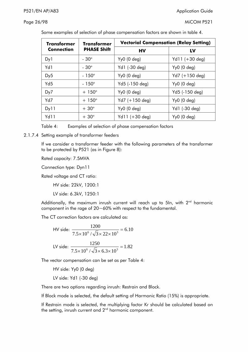
P521/EN AP/A83 Application Guide Page 26/98 MiCOM P521
Some examples of selection of phase compensation factors are shown in table 4.
Vectorial Compensation (Relay Setting) Transformer Connection
Transformer PHASE Shift HV LV
Dy1 - 30o Yy0 (0 deg) Yd11 (+30 deg)
Yd1 - 30o Yd1 (-30 deg) Yy0 (0 deg)
Dy5 - 150o Yy0 (0 deg) Yd7 (+150 deg)
Yd5 - 150o Yd5 (-150 deg) Yy0 (0 deg)
Dy7 + 150o Yy0 (0 deg) Yd5 (-150 deg)
Yd7 + 150o Yd7 (+150 deg) Yy0 (0 deg)
Dy11 + 30o Yy0 (0 deg) Yd1 (-30 deg)
Yd11 + 30o Yd11 (+30 deg) Yy0 (0 deg)
Table 4: Examples of selection of phase compensation factors
2.1.7.4 Setting example of transformer feeders
If we consider a transformer feeder with the following parameters of the transformer to be protected by P521 (as in Figure 8):
Rated capacity: 7.5MVA
Connection type: Dyn11
Rated voltage and CT ratio:
HV side: 22kV, 1200:1
LV side: 6.3kV, 1250:1
Additionally, the maximum inrush current will reach up to 5In, with 2nd harmonic component in the rage of 20~60% with respect to the fundamental.
The CT correction factors are calculated as:
HV side: 10.610223/105.7
120036
=×××
LV side: 82.1103.63/105.7
125036
=×××
The vector compensation can be set as per Table 4:
HV side: Yy0 (0 deg)
LV side: Yd1 (-30 deg)
There are two options regarding inrush: Restrain and Block.
If Block mode is selected, the default setting of Harmonic Ratio (15%) is appropriate.
If Restrain mode is selected, the multiplying factor Kr should be calculated based on the setting, inrush current and 2nd harmonic component.
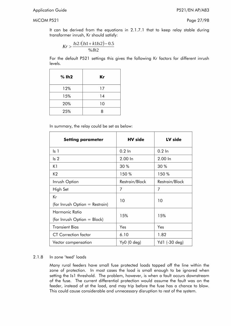
Application Guide P521/EN AP/A83 MiCOM P521 Page 27/98
It can be derived from the equations in 2.1.7.1 that to keep relay stable during transformer inrush, Kr should satisfy:
( )
2%5.0211/2
IhIskIsIsKr −+
>
For the default P521 settings this gives the following Kr factors for different inrush levels.
% Ih2 Kr
12% 17
15% 14
20% 10
25% 8
In summary, the relay could be set as below:
Setting parameter HV side LV side
Is 1 0.2 In 0.2 In
Is 2 2.00 In 2.00 In
K1 30 % 30 %
K2 150 % 150 %
Inrush Option Restrain/Block Restrain/Block
High Set 7 7
Kr
(for Inrush Option = Restrain) 10 10
Harmonic Ratio
(for Inrush Option = Block) 15% 15%
Transient Bias Yes Yes
CT Correction factor 6.10 1.82
Vector compensation Yy0 (0 deg) Yd1 (-30 deg)
2.1.8 In zone ‘teed’ loads
Many rural feeders have small fuse protected loads tapped off the line within the zone of protection. In most cases the load is small enough to be ignored when setting the Ιs1 threshold. The problem, however, is when a fault occurs downstream of the fuse. The current differential protection would assume the fault was on the feeder, instead of at the load, and may trip before the fuse has a chance to blow. This could cause considerable and unnecessary disruption to rest of the system.

P521/EN AP/A83 Application Guide Page 28/98 MiCOM P521
To prevent this from occurring the operating time of the current differential element can be time delayed to grade with the fuse. The time delay can be either definite time (DMT) or Inverse time (ΙDMT), selectable in the “ΙDiff Delay Type” cell under PROTECTION G1 (G2)/[87] Current Diff. If DMT is chosen the relay can be set with a definite time delay setting. If, however, ΙDMT is chosen a curve and its associated TMS/Time dial can be selected to grade with the fuse. To reduce fault clearance times for heavy internal faults the ΙDMT delay type is preferable as the operating time reduces for larger fault currents.
2.2 Overcurrent and earth fault protection
The overcurrent and earth fault protection is provided as an alternative form of back-up protection. The P521 relay has four stages overcurrent and four stages of earth fault. The first two stages have a selectable ΙDMT or DMT characteristic. The third and fourth stages have a DMT characteristic only. The overcurrent and earth fault protection can be selectively enabled or disabled in the “Ι> ?” cell (Yes = enabled, No = disabled). A feature also exists whereby the protection can be enabled upon failure of the differential protection communication channel (select “backup” in the “Ι> ?” cell).
The overcurrent protection stages are labeled Ι>/tΙ>, Ι>>/tΙ>>, Ι>>>/tΙ>>> and Ι>>>>/tΙ>>>>. The earth fault protection stages are labeled Ιe>/tΙe>, Ιe>>/tΙe>>, Ιe>>>/tΙe>>> and Ιe>>>>/tΙe>>>>.
Figure 9 shows the logic associated with the first stage phase overcurrent protection (Ι>/tΙ>). Figure 9 shows the logic for overcurrent stages two, three and four (logic is duplicated for each stage). The logic diagrams in Figure 9 and Figure 10 are identical, which is why the earth fault logic is not shown.

Application Guide P521/EN AP/A83 MiCOM P521 Page 29/98
789:;
<<9
<
789::
9
<
< 7=9
;>?:
;;:<
@ A!
9
8!
>
"#
9 !$
B
"!9
8!
>
B B
;%:# !
;%:#9
8!
>
!B
Figure 9 First stage phase overcurrent protection (Ι>/tΙ>) logic
!"!# $% &'
(
)%
*
+
'%,
$%$,,,
-./) 0-
10 .&'2
10 3 . "4
% "4
+
45
60<
70* ',%
70*
)%
-./) 30/-0
Figure 10 Logic for overcurrent stages two, three and four
Note: Both the overcurrent and earth fault protection operate from only the fundamental component of the line current.

P521/EN AP/A83 Application Guide Page 30/98 MiCOM P521
The overcurrent and earth fault elements will need to be co-ordinated with any other protection elements on the system, in order to provide discriminative fault clearance. The overcurrent menu column is shown in table 5 below followed by the earth fault settings in table 6.
[50/51] Phase OC
Default Setting
Min Max Step
Ι> ? No Yes, No, Backup
Ι> 1 Ιn 0.1 Ιn 25 Ιn 0.01 Ιn
Ι> Delay Type DMT DMT, ΙDMT, RΙ
tΙ> 40 ms 0 s 150 s 0.01 s
Ι> Curve ΙEC SΙ ΙEC STΙ, ΙEC SΙ, ΙEC VΙ, ΙEC EΙ, ΙEC LTΙ, CO2, ΙEEE MΙ, CO8, ΙEEE VΙ, ΙEEE EΙ
Ι> Tms 1 0.025 1.5 0.025
Ι> Time Dial 1 0.1 100 0.1
K 0.1 0.1 10 0.005
Reset Type DMT DMT ΙDMT N/A
tReset 40 ms 40 ms 100 s 0.01 s
Rtms 0.025 0.025 3.2 0.025
Ι> ? No Yes, No, Backup
Ι>> 1 Ιn 0.5 Ιn 40 Ιn 0.05 Ιn
Remaining Ι>> cells are identical to Ι> above
Ι>>> ? No Yes, No, Backup
Ι>>> 20 Ιn 0.5 Ιn 40 Ιn 0.05 Ιn
tΙ>>> 10 ms 0 s 150 s 0.01 s
Ι>>>> ? No Yes, No, Backup
Ι>>>> 20 Ιn 0.5 Ιn 40 Ιn 0.05 Ιn
tΙ>>>> 10 ms 0 s 150 s 0.01 s
Table 5: Overcurrent protection settings
[50N/51N] E/Gnd
Default Setting
Min Max Step
Ιe> ? Yes Yes, No, Backup
Ιe> 0.1 Ιen*, 0.01 Ιen**, 0.002 Ιen***
0.1 Ιen*, 0.01 Ιen**, 0.002 Ιen***
25 Ιen*, 1 Ιen**, 1 Ιen***
0.01 Ιen*, 0.005 Ιen**, 0.001***
Ιe> Delay Type DMT DMT, ΙDMT, RΙ, LABOR
tΙe> 40 ms 0 s 150 s 0.01 s
Ιe> Curve ΙEC SΙ ΙEC STΙ, ΙEC SΙ, ΙEC VΙ, ΙEC EΙ, ΙEC LTΙ,
CO2, ΙEEE MΙ, CO8, ΙEEE EΙ; 1, 2, 3
Ιe> Tms 1 0.025 1.5 0.025

Application Guide P521/EN AP/A83 MiCOM P521 Page 31/98
[50N/51N] E/Gnd
Default Setting
Min Max Step
Ιe> Time Dial 1 0.1 100 0.1
K 0.1 0.1 10 0.005
Reset Type DMT DMT ΙDMT N/A
tReset 40 ms 40 ms 100 s 0.01 s
Rtms 0.025 0.025 3.2 0.025
Ιe>> ? No Yes, No, Backup
Ιe>> 1 Ιn 0.5 Ιen*, 0.01 Ιen**, 0.002 Ιen***
40 Ιen*, 8 Ιen**, 1 Ιen***
0.01 Ιen*, 0.005 Ιen**, 0.001 Ιen***
Remaining Ιe>> cells are identical to Ιe> above
Ιe>>> ? No Yes, No, Backup
Ιe>>> 1 Ιn 0.5 Ιen*, 0.01 Ιen**, 0.002 Ιen***
40 Ιen*, 8 Ιen**, 1 Ιen***
0.01 Ιen*, 0.005 Ιen**, 0.001 Ιen***
tΙe>>> 10 ms 0 s 150 s 0.01 s
Ιe>>>> ? No Yes, No, Backup
Ιe>>>> 20 Ιn 0.5 Ιen*, 0.01 Ιen**, 0.002 Ιen***
40 Ιen*, 8 Ιen**, 1 Ιen***
0.01 Ιen*, 0.005 Ιen**, 0.001 Ιen***
tΙe>>>> 10 ms 0 s 150 s 0.01s
Table 6: Earth fault protection settings
* - denotes the standard earth fault board (0.1 to 40 Ιen)
** - denotes the sensitive earth fault board (0.01 to 8 Ιen)
*** - denotes the very sensitive earth fault board (0.002 to 1 Ιen)
2.2.1 Instantaneous (start) function (50/50N)
As soon as a phase (earth) threshold is exceeded, the instantaneous (start) output associated with this threshold is active. This output indicates that the protection has detected a phase (earth) fault and that the time delay associated with the threshold has started. This time delay can be blocked via the logic input "Blk Log" associated with this threshold. If this blocking input is activated by an output contact of a downstream relay, operation is blocked so that the relay closest to the fault can trip. This principle is known as «Blocking logic» or merely «Blocking». It is described in more detail later in this document.
2.2.2 Definite time operation (DMT)
The four phase (earth) overcurrent thresholds can be selected with a definite time delay. The operating time is equal to the set time delay, plus the operating time of the output contact (typically 20 to 30 ms; 20 ms for a current greater than or equal to twice the threshold) and the time required to detect the overcurrent state (maximum 20 ms at 50 Hz and 16.7 ms at 60 Hz).

P521/EN AP/A83 Application Guide Page 32/98 MiCOM P521
2.2.3 ΙDMT thresholds
2.2.3.1 Inverse time curves
The first and second phase (earth) overcurrent thresholds can be selected with an inverse time characteristic (ΙDMT). There are eleven ΙDMT characteristics in total. The operating time for all but the RI curve can be calculated with the following equation. The sensitive earth fault protection (0.01 to 8 Ιen) has 3 additional LABORELEC curves. These are explained in section 2.2.4.
t = T x ⎝⎜⎛
⎠⎟⎞
K ,, (Ι/Ιs) α - 1 + L
Where:
t = Operating time (seconds)
K = Constant (see table 7)
Ι = Value of measured current
ΙS = Value of the selected threshold (Pick-up value)
α = Constant (see table 7)
L = ANSI/IEEE coefficient (zero for ΙEC curves)
T = Time multiplier setting (Tms) for ΙEC curves or Time Dial for ΙEEE/CO2/CO8 curves.
Type of Curve Standard K Factor α Factor L Factor
ΙEC STI (Short Time Inverse) ΙEC 0.05 0.04 0
ΙEC SI (Standard Inverse) ΙEC 0.14 0.02 0
ΙEC VI (Very Inverse) ΙEC 13.5 1 0
ΙEC EI (Extremely Inverse) ΙEC 80 2 0
UK LTI (Long Time Inverse) UK 120 1 0
CO2 (Short Time Inverse) CO2 0.02394 0.02 0.01694
ΙEEE MI (Moderately Inverse) ANSI/ΙEEE 0.0515 0.02 0.114
CO8 (Inverse) CO8 5.95 2 0.18
ΙEEE VI (Very Inverse) ANSI/ΙEEE 19.61 2 0.491
ΙEEE EI (Extremely Inverse) ANSI/ΙEEE 28.2 2 0.1215
Table 7: ΙDMT characteristic coefficients
The operating time for the RI curve (electromechanical) is given by the following formula:
t = K x ( ) 1,, 0.339 - 0.236 /(Ι/Ιs)
With K adjustable from 0.10 to 10 in steps of 0.05
This equation is valid for 1.1<= (I/Is) <= 20
Although the curves tend towards infinity, as the current approaches Is, the minimum guaranteed current, for all inverse time characteristics, is 1.1Ιs (with a tolerance of ±0.05Ιs). If DMT (definite time characteristic) is chosen the minimum operating current is equal to the selected threshold, which also has a tolerance of ±0.05Ιs.
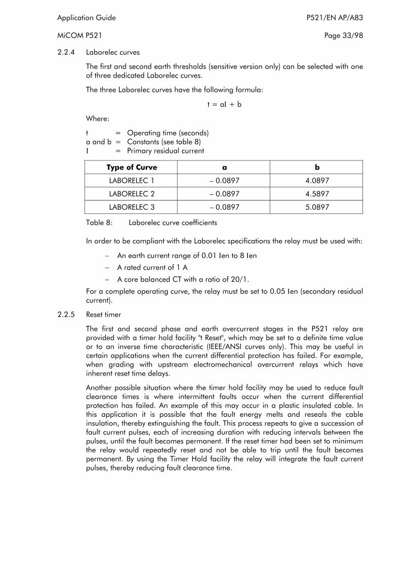
Application Guide P521/EN AP/A83 MiCOM P521 Page 33/98
2.2.4 Laborelec curves
The first and second earth thresholds (sensitive version only) can be selected with one of three dedicated Laborelec curves.
The three Laborelec curves have the following formula:
t = aΙ + b
Where:
t = Operating time (seconds) a and b = Constants (see table 8) I = Primary residual current
Type of Curve a b
LABORELEC 1 – 0.0897 4.0897
LABORELEC 2 – 0.0897 4.5897
LABORELEC 3 – 0.0897 5.0897
Table 8: Laborelec curve coefficients
In order to be compliant with the Laborelec specifications the relay must be used with:
− An earth current range of 0.01 Ιen to 8 Ιen
− A rated current of 1 A
− A core balanced CT with a ratio of 20/1.
For a complete operating curve, the relay must be set to 0.05 Ιen (secondary residual current).
2.2.5 Reset timer
The first and second phase and earth overcurrent stages in the P521 relay are provided with a timer hold facility "t Reset", which may be set to a definite time value or to an inverse time characteristic (IEEE/ANSI curves only). This may be useful in certain applications when the current differential protection has failed. For example, when grading with upstream electromechanical overcurrent relays which have inherent reset time delays.
Another possible situation where the timer hold facility may be used to reduce fault clearance times is where intermittent faults occur when the current differential protection has failed. An example of this may occur in a plastic insulated cable. In this application it is possible that the fault energy melts and reseals the cable insulation, thereby extinguishing the fault. This process repeats to give a succession of fault current pulses, each of increasing duration with reducing intervals between the pulses, until the fault becomes permanent. If the reset timer had been set to minimum the relay would repeatedly reset and not be able to trip until the fault becomes permanent. By using the Timer Hold facility the relay will integrate the fault current pulses, thereby reducing fault clearance time.

P521/EN AP/A83 Application Guide Page 34/98 MiCOM P521
If the first and second phase (earth) threshold is selected with an ΙDMT IEC or RI curve, the reset timer "t Reset" has a definite time characteristic, settable between 40 ms and 100 s in steps of 10 ms. The reset time “tReset” can be found in the following locations:
− PROTECTION G1 (G2)/[50/51] Phase OC /t Reset
and
− PROTECTION G1 (G2)/[50N/51N] E/Gnd /t Reset
If the first phase (earth) threshold is selected with an ΙDMT IEEE or CO curve, the reset timer can be set either DMT or ΙDMT in the “Reset Type” cell. If DMT is chosen the reset time becomes definite time with the time set in the "t Reset" cell. If ΙDMT is chosen the reset time is based upon an inverse curve which is current dependent. A time multiplier “Rtms” can also be applied to this curve so that it can be tailored to the application. The reset function menu cells are located as follows:
− PROTECTION G1 (G2)/[50/51] Phase OC /Reset Type
− PROTECTION G1 (G2)/[50/51] Phase OC /t Reset (if Reset Type = DMT)
− PROTECTION G1 (G2)/[50/51] Phase OC /Rtms (if Reset Type = ΙDMT)
and
− PROTECTION G1 (G2)/[50N/51N] E/Gnd /Reset Type
− PROTECTION G1 (G2)/[50N/51N] Phase OC /t Reset (if Reset Type = DMT)
− PROTECTION G1 (G2)/[50N/51N] Phase OC /Rtms (if Reset Type = ΙDMT)
The ΙDMT reset time is dependent upon the chosen operating time curve and the selected “Rtms” value. The ΙDMT reset time formula, applicable to the 5 CO/ANSI/IEEE curves, is as follows:
t = T x ⎝⎛
⎠⎞K ,, 1 - (Ι/Ιs) 2
Where: t = Reset time
K = Constant (see table 9)
Ι = Value of the measured current
ΙS = Value of the selected threshold (pick-up value)
T = Reset Time Multiplier (Rtms) between 0.025 and 3.2
Type of Curves Standard K Factor
CO2 (Short time inverse) CO2 2.261
IEEE MI (Moderately inverse) ANSI/IEEE 4.85
CO8 (Inverse) CO8 5.95
IEEE VI (Very inverse) ANSI/IEEE 21.6
IEEE EI (Extremely inverse) ANSI/IEEE 29.1
Table 9: Reset curve coefficients

Application Guide P521/EN AP/A83 MiCOM P521 Page 35/98
2.2.6 Time graded protection
Inverse definite minimum time relays are time graded such that the relay nearer to the fault operates faster than the upstream relays. This is referred to as relay co-ordination because if the relay nearest to the fault fails operate, the upstream relay will trip in a slightly longer time. The time grading steps are typically 400 ms, therefore the operating time for each upstream relay becomes progressively longer.
Where difficulty is experienced in arranging the required time grading steps the use of a blocked overcurrent scheme should be considered (described in a later section).
2.3 Thermal overload protection
Thermal overload protection can be used to prevent electrical plant from operating at temperatures in excess of the designed maximum withstand. Prolonged overloading causes excessive heating, which may result in premature deterioration of the insulation, or in extreme cases, insulation failure.
The MiCOM P521 incorporates a current based thermal replica, using the RMS load current to model the heating and cooling of the protected plant. The element can be set with both alarm and trip stages.
The heat generated within an item of plant, such as a cable or a transformer, is created by the resistive loss (Ι2R x t). Thus, heating is directly proportional to current squared. The thermal time characteristic used in the relay is therefore based on current squared, integrated over time. MiCOM relays automatically use the largest phase current for input to the thermal model.
Equipment is designed to operate continuously at a temperature corresponding to its full load rating, where heat generated is balanced with heat dissipated by radiation etc. Over-temperature conditions therefore occur when currents in excess of rating are allowed to flow for a period of time. It can be shown that temperatures during heating follow exponential time constants and a similar exponential decrease of temperature occurs during cooling.
In order to apply this protection element, the thermal time constant for the protected item of plant is therefore required. The settings associated with the thermal menu are shown in table 10. These settings can found under PROTECTION G1 (G2)/[49] Therm OL.
[49] Thermal OL
Default Setting
Min Max Step
Therm OL ? No Yes, No
Ιθ> 1 Ιn 0.1 Ιn 3.2 Ιn 0.01 Ιn
Te 1 mn 1 mn 200 mn 1 mn
K 1.05 1 1.5 0.01
θ Trip 100% 50% 200% 1%
θ Alarm ? No Yes, No
θ Alarm 90% 50% 200% 1%
Table 10: Thermal overload settings
The following sections will show that different items of plant possess different thermal characteristics, due to the nature of their construction.

P521/EN AP/A83 Application Guide Page 36/98 MiCOM P521
2.3.1 Thermal overload characteristic
This characteristic is used to protect cables, dry type transformers (e.g. type AN), and capacitor banks. When protecting these devices, the trip time varies depending on the load current carried before application of the overload, i.e. whether the overload was applied from “hot” or “cold”.
Curves of the thermal overload time characteristic are given in the Technical Data and Curve Characteristics (P521/EN TD) section of the service manual.
The operating time of the thermal element is given by:
Ttrip = Te. loge
⎝⎜⎜⎛
⎠⎟⎟⎞K2 - ( )Ιp/Ιθ>
2
K2 - Trip2
With:
Ttrip = Time to trip (in seconds).
Te = Thermal time constant of the protected element (in seconds).
K = Thermal overload equal to Ιeq/k Ιθ >.
Ιeq = Equivalent current, corresponds to the RMS value of the largest phase current.
Ιθ> = Thermal current setting.
k = Overload factor by which the Ιθ> setting must be multiplied to determine the trip threshold.
Ιp = Steady state pre-loading before application of the overload.
Trip = Trip thermal state. If the trip thermal state is set at 100%, then Trip = 1
The calculation of the thermal state is given by the following formula:
θι+1 = ( Ιeq/ Iθ >)2 [1- exp(-t/Te)] + θι exp(-t/Te)
θ being calculated every 100 ms
2.3.2 Setting guidelines
The thermal trip level in terms of current can be determined as follows:
Thermal trip = Trip x K2
100 x 1θ>
Note: The ‘Trip’ setting must be entered as a percentage i.e. 90 for 90%.
There are two methods of setting the Ιθ> and ‘k’ settings in the P521. The selected method may depend upon company standards or personal preference. This also assumes that the ‘Trip’ value is set to 100%.
The first method assumes that the Ιθ> setting is set to the maximum current that the plant can withstand before it becomes damaged. This is normally greater than the permissible continuous load current. In this case the plant can not tolerate any further loading, which means the overload factor ‘k’ should be set to 1. Hence the thermal trip level, in amps, will be equal to Ιθ>.
If, however, the Ιθ> setting was set equal to the permissible continuous load current, an overload factor ‘k’ may be applied, since it is likely that the plant has been designed to tolerate a current in excess of this amount. For example, if a line has a permissible continuous load current of 762 A (Ιθ> setting), but the line can actually tolerate 800 A, the ‘k’ factor can set to 1.05 (800 A/762 A). Hence the thermal trip level, in amps, will be ‘k x Ιθ>’.
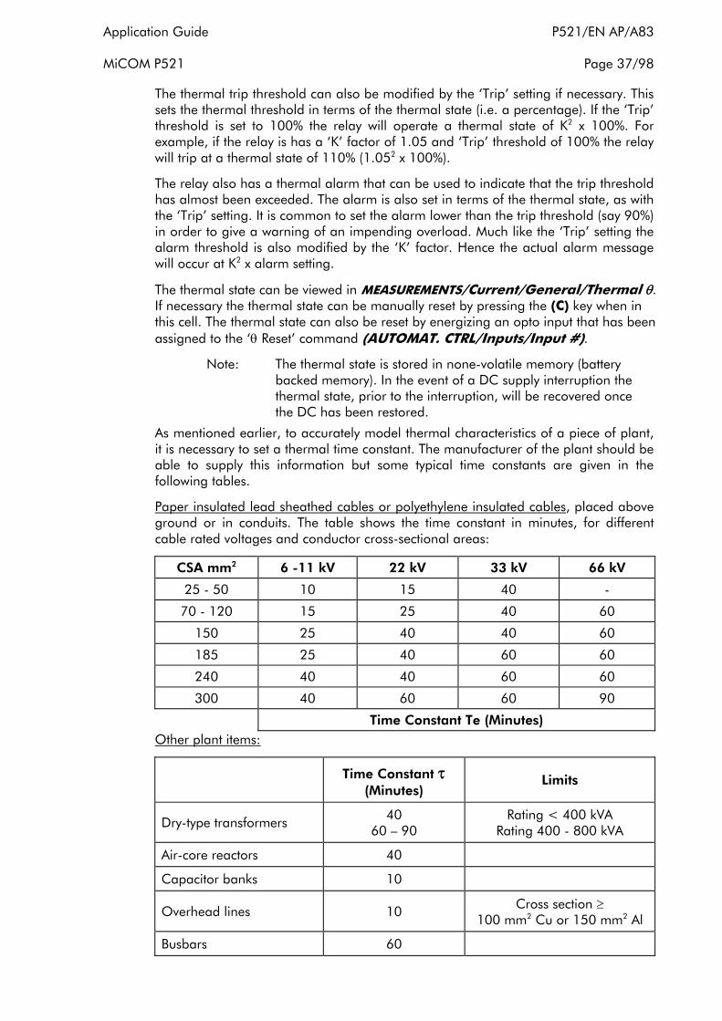
Application Guide P521/EN AP/A83 MiCOM P521 Page 37/98
The thermal trip threshold can also be modified by the ‘Trip’ setting if necessary. This sets the thermal threshold in terms of the thermal state (i.e. a percentage). If the ‘Trip’ threshold is set to 100% the relay will operate a thermal state of K2 x 100%. For example, if the relay is has a ‘K’ factor of 1.05 and ‘Trip’ threshold of 100% the relay will trip at a thermal state of 110% (1.052 x 100%).
The relay also has a thermal alarm that can be used to indicate that the trip threshold has almost been exceeded. The alarm is also set in terms of the thermal state, as with the ‘Trip’ setting. It is common to set the alarm lower than the trip threshold (say 90%) in order to give a warning of an impending overload. Much like the ‘Trip’ setting the alarm threshold is also modified by the ‘K’ factor. Hence the actual alarm message will occur at K2 x alarm setting.
The thermal state can be viewed in MEASUREMENTS/Current/General/Thermal θ. If necessary the thermal state can be manually reset by pressing the (C) key when in this cell. The thermal state can also be reset by energizing an opto input that has been assigned to the ‘θ Reset’ command (AUTOMAT. CTRL/Inputs/Input #).
Note: The thermal state is stored in none-volatile memory (battery backed memory). In the event of a DC supply interruption the thermal state, prior to the interruption, will be recovered once the DC has been restored.
As mentioned earlier, to accurately model thermal characteristics of a piece of plant, it is necessary to set a thermal time constant. The manufacturer of the plant should be able to supply this information but some typical time constants are given in the following tables.
Paper insulated lead sheathed cables or polyethylene insulated cables, placed above ground or in conduits. The table shows the time constant in minutes, for different cable rated voltages and conductor cross-sectional areas:
CSA mm2 6 -11 kV 22 kV 33 kV 66 kV
25 - 50 10 15 40 -
70 - 120 15 25 40 60
150 25 40 40 60
185 25 40 60 60
240 40 40 60 60
300 40 60 60 90
Time Constant Te (Minutes) Other plant items:
Time Constant τ (Minutes)
Limits
Dry-type transformers 40 60 – 90
Rating < 400 kVA Rating 400 - 800 kVA
Air-core reactors 40
Capacitor banks 10
Overhead lines 10 Cross section ≥ 100 mm2 Cu or 150 mm2 Al
Busbars 60

P521/EN AP/A83 Application Guide Page 38/98 MiCOM P521
2.4 Circuit breaker failure protection (CBF)
Following inception of a fault one or more main protection devices will operate and issue a trip output to the circuit breaker(s) associated with the faulted circuit. Operation of the circuit breaker is essential to isolate the fault, and prevent damage/further damage to the power system.
For transmission/sub-transmission systems, slow fault clearance can also threaten system stability. It is therefore common practice to install circuit breaker failure protection, which monitors that the circuit breaker has opened within a reasonable time. If the fault current has not been interrupted following a set time delay from circuit breaker trip initiation, breaker failure protection (CBF) will operate.
CBF operation can be used to backtrip upstream circuit breakers to ensure that the fault is isolated correctly. CBF operation can also reset all start output contacts, ensuring that any blocks asserted on upstream protection are removed.
The settings associated with the circuit breaker fail protection is shown in table 11 below. They can be found in AUTOMAT. CTRL/CB Fail.
CB Fail Default Setting
Min Max Step
CB Fail ? No Yes, No
Ι< 0.1 Ιn 0.02 Ιn 1 Ιn 0.01 Ιn
CB Fail Time tBF 100 ms 30 ms 10 s 0.01 s
Block Ι> ? No Yes, No
Block Ιe> ? No Yes, No
Table 11: Circuit breaker fail settings
2.4.1 Circuit breaker failure protection operation
When a trip order is given through the output relay RL1, the t BF timer is started. The trip order can be issued either from a protection element, or a logic input. In order to initiate the tBF timer by a logic input the ‘Start tBF’ command must be assigned to that input (AUTOMAT. CTRL/Inputs/Input #). The MiCOM relay then monitors the currents in each phase and compares them with the zone defined by the undercurrent Ι< threshold (not to be confused with the [37] under current protection function). This threshold value is settable within the AUTOMAT. CTRL/CB Fail menu.
Following the start of the t BF timer, the relay detects the first time that current goes out of the Ι< zone. On detection of this transition, the relay starts another timer which has a non-settable duration of 20 samples.
Since the relay sampling rate is 32 samples by cycle, this timer duration is 12.5 ms for a 50 Hz system and 10.4 ms for a 60 Hz system. During this time, the relay is checking if the current goes out of the Ι< zone again. In the case where the current is not switched off (CB has failed to trip), the current signal should again go out of the Ι< zone at a time equal to 16 samples after the former detection (i.e. half a cycle).
Each time the relay detects the current going out of the Ι< zone, the relay once again starts a timer which has a duration of 20 samples and it checks if the current goes out of the Ι< zone once again.
In the window of 20 samples, the relay checks that the current signal going out of the Ι< zone is in the opposite direction.

Application Guide P521/EN AP/A83 MiCOM P521 Page 39/98
• If there is no current signal going out in the opposite direction within the 20 sample duration, the relay states that the CB pole has opened. The « CB pole open » internal signal is then initiated.
• If there is a current signal going out in opposite direction within the 20 sample duration the relay states that the CB pole has not yet opened. The « CB pole closed » internal signal is maintained.
Once the t BF time delay has elapsed, the relay checks the status of the « CB pole » internal signal for each pole of the circuit breaker. If one or more internal signals indicate that their CB poles have not yet opened, the relay initiates the CB FAIL signal. The CB fail signal can be arranged to remove the start signals of the Ι> and Ιe> elements, in order to remove blocking signals from any upstream protection. Alternatively, the CB fail signal can operate a selectable contact (AUTOMAT. CTRL/ Output relays/ CB Fail).
This contact can be used to backtrip upstream switchgear, generally tripping all infeeds connected to the same busbar section.
To remove the Ι> and Ιe> start signals once the breaker fail timer has elapsed the following cells must be set to ‘Yes’:
− AUTOMAT. CTRL/CB Fail/Block Ι> ? and
− AUTOMAT. CTRL /CB Fail/Block Ιe> ? As mentioned earlier the CB fail timer can be started by an external input that can be connected to external protection equipment. Note the option to start the CB fail detection function by a digital input (labeled Strt TBF) without a trip order given by the MiCOM relay. In this case the tBF timer starts from the digital input. If the CB is not opened (by an another protection relay) at the end of tBF, the MiCOM relay outputs the CB FAIL signal.
It is possible to automatically send a direct intertrip command to the remote relay whenever a CB fail condition occurs. This is enabled by selecting ‘Yes’ in the “I-Trip CB Fail” cell (AUTOMAT. CTRL/I-Trip Commands).
Figure 11 shows a CB Fail detection start following a trip command:

P521/EN AP/A83 Application Guide Page 40/98 MiCOM P521
&C..!
'"
(!""
0"
0"
0" 0" 0" 0" 0"
0" 0" 0" 0" 0"
&C..!
00)
Figure 11 CB fail detection principle
The Figure 12 shows a normal CB operation before tBF expires. No CB fail signal is given.
! ""
! ""
#
Figure 12 CB open before TBF expired
Figure 13 below shows a CB failure condition. At the drop off of the t BF timer, the relay has not detected an opening of the CB pole, hence a CB FAIL signal is initiated.

Application Guide P521/EN AP/A83 MiCOM P521 Page 41/98
! ""
! ""
$% &
Figure 13 CB not yet open before TBF expired
The Figure 14 shows another case of normal CB operation. On fault clearance, the removal of the phase current signal takes time, often due to the de-energization of the phase CT. This is a typical case for TPY class CTs which are built with an air gap in their magnetic core. Before the drop off of the t BF timer, the relay has detected an opening of the CB pole, thus no CB failure signal is given. A basic Breaker Failure element based on a simple undercurrent element would detect a false CB failure condition as the current signal value is still outside the Ι< zone after the t BF timer has elapsed.
Note: Both « CB pole closed » and « CB pole opened » internal signals mentioned in the above diagrams are derived from the Circuit Breaker Failure function algorithm. They are not affected by the status of the relay opto-inputs wired to the 52a and 52b CB auxiliary contacts.
! ""
! ""
'
Figure 14 De-energization of the phase CT

P521/EN AP/A83 Application Guide Page 42/98 MiCOM P521
2.4.2 Breaker fail timer settings
A typical timer setting used with a 2½ cycle circuit breaker is around 150 ms.
2.4.3 Breaker fail undercurrent settings
The phase undercurrent settings (Ι<) must be set to less than load current, to ensure that Ι< operation indicates that the circuit breaker pole is open. A typical setting for overhead lines or cable circuits is 20% Ιn.
2.4.4 CBF fail logic
Figure 15 shows the logic associated with circuit breaker failure protection.
8
' 1, %
8
8
+
-. ,
-./) ' ' ,
'
(
)%
'
(
)%
10 3
+
3
3
4!
60
70* ',%
70* '
)%
Figure 15 Circuit breaker failure protection logic
2.5 Broken conductor detection
The majority of faults on a power system occur between one phase and ground or two phases and ground. These are known as shunt faults and arise from lightning discharges and other overvoltages which initiate flashovers. Alternatively, they may arise from other causes such as birds on overhead lines or mechanical damage to cables etc. Such faults result in an appreciable increase in current and in the majority of applications are easily detectable.
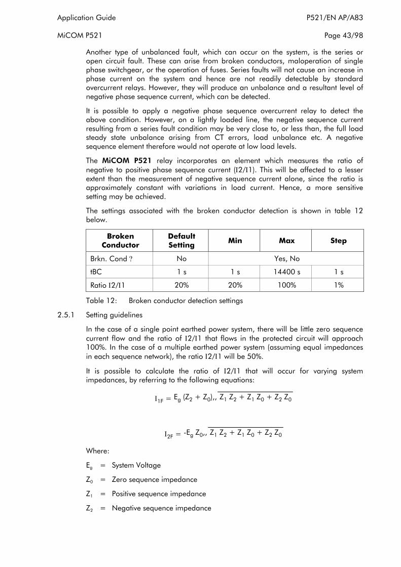
Application Guide P521/EN AP/A83 MiCOM P521 Page 43/98
Another type of unbalanced fault, which can occur on the system, is the series or open circuit fault. These can arise from broken conductors, maloperation of single phase switchgear, or the operation of fuses. Series faults will not cause an increase in phase current on the system and hence are not readily detectable by standard overcurrent relays. However, they will produce an unbalance and a resultant level of negative phase sequence current, which can be detected.
It is possible to apply a negative phase sequence overcurrent relay to detect the above condition. However, on a lightly loaded line, the negative sequence current resulting from a series fault condition may be very close to, or less than, the full load steady state unbalance arising from CT errors, load unbalance etc. A negative sequence element therefore would not operate at low load levels.
The MiCOM P521 relay incorporates an element which measures the ratio of negative to positive phase sequence current (Ι2/Ι1). This will be affected to a lesser extent than the measurement of negative sequence current alone, since the ratio is approximately constant with variations in load current. Hence, a more sensitive setting may be achieved.
The settings associated with the broken conductor detection is shown in table 12 below.
Broken Conductor
Default Setting
Min Max Step
Brkn. Cond ? No Yes, No
tBC 1 s 1 s 14400 s 1 s
Ratio Ι2/Ι1 20% 20% 100% 1%
Table 12: Broken conductor detection settings
2.5.1 Setting guidelines
In the case of a single point earthed power system, there will be little zero sequence current flow and the ratio of Ι2/Ι1 that flows in the protected circuit will approach 100%. In the case of a multiple earthed power system (assuming equal impedances in each sequence network), the ratio Ι2/Ι1 will be 50%.
It is possible to calculate the ratio of Ι2/Ι1 that will occur for varying system impedances, by referring to the following equations:
Ι1F = Eg (Z2 + Z0),, Z1 Z2 + Z1 Z0 + Z2 Z0
Ι2F = -Eg Z0,, Z1 Z2 + Z1 Z0 + Z2 Z0
Where:
Eg = System Voltage
Z0 = Zero sequence impedance
Z1 = Positive sequence impedance
Z2 = Negative sequence impedance

P521/EN AP/A83 Application Guide Page 44/98 MiCOM P521
Therefore:
Ι2F, Ι1F = Z0,, Z0 + Z2
It follows that, for an open circuit in a particular part of the system, Ι2/Ι1 can be determined from the ratio of zero sequence to negative sequence impedance. It must be noted however, that this ratio may vary depending upon the fault location. It is desirable therefore to apply as sensitive a setting as possible. In practice, this minimum setting is governed by the levels of standing negative phase sequence current present on the system. This can be determined from a system study, or by making use of the relay measurement facilities at the commissioning stage. If the latter method is adopted, it is important to take the measurements during maximum system load conditions, to ensure that all single phase loads are accounted for.
Since sensitive settings are employed, it can be expected that the element will operate for any unbalance condition occurring on the system (for example, during a single pole auto-reclose cycle). Therefore, a long time delay is necessary to ensure co-ordination with other protective devices. A 60 second time delay setting may be typical.
2.5.2 Example setting
The following information was recorded by the relay during commissioning;
Ιfull load = 500 A
Ι2 = 50 A
Therefore the quiescent Ι2/Ι1 ratio is given by:
Ι2/Ι1 = 50/500 = 0.1
To allow for tolerances and load variations a setting of 200% of this value may be typical: Therefore set RATIO Ι2/Ι1 = 20%
Set tBC = 60 s to allow adequate time for short circuit fault clearance by time delayed protections.
2.6 Intertripping facilities
2.6.1 Permissive intertrip
The P521 relay includes a facility to send a permissive intertrip command over the protection communication channel, as shown in Figure 16.
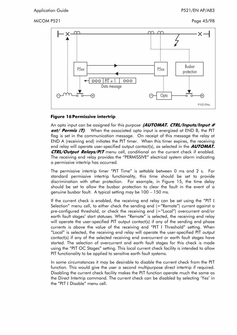
Application Guide P521/EN AP/A83 MiCOM P521 Page 45/98
"
11 11
Figure 16 Permissive intertrip
An opto input can be assigned for this purpose (AUTOMAT. CTRL/Inputs/Input # ext/ Permis ΙT). When the associated opto input is energized at END B, the PΙT flag is set in the communication message. On receipt of this message the relay at END A (receiving end) initiates the PΙT timer. When this timer expires, the receiving end relay will operate user-specified output contact(s), as selected in the AUTOMAT. CTRL/Output Relays/PΙT menu cell, conditional on the current check if enabled. The receiving end relay provides the “PERMISSIVE” electrical system alarm indicating a permissive intertrip has occurred.
The permissive intertrip timer “PΙT Time” is settable between 0 ms and 2 s. For standard permissive intertrip functionality, this time should be set to provide discrimination with other protection. For example, in Figure 15, the time delay should be set to allow the busbar protection to clear the fault in the event of a genuine busbar fault. A typical setting may be 100 – 150 ms.
If the current check is enabled, the receiving end relay can be set using the “PΙT Ι Selection” menu cell, to either check the sending end (=“Remote”) current against a pre-configured threshold, or check the receiving end (=“Local”) overcurrent and/or earth fault stages’ start statuses. When “Remote” is selected, the receiving end relay will operate the user-specified PIT output contact(s) if any of the sending end phase currents is above the value of the receiving end “PΙT Ι Threshold” setting. When “Local” is selected, the receiving end relay will operate the user-specified PIT output contact(s) if any of the selected receiving end overcurrent or earth fault stages have started. The selection of overcurrent and earth fault stages for this check is made using the “PΙT OC Stages” setting. This local current check facility is intended to allow PIT functionality to be applied to sensitive earth fault systems.
In some circumstances it may be desirable to disable the current check from the PΙT function. This would give the user a second multipurpose direct intertrip if required. Disabling the current check facility makes the PΙT function operate much the same as the Direct Intertrip command. The current check can be disabled by selecting ‘Yes’ in the “PΙT Ι Disable” menu cell.

P521/EN AP/A83 Application Guide Page 46/98 MiCOM P521
The PΙT function menu cells are located as follows:
− PROTECTION G1 (G2)/[87] Current Diff /PΙT Time
− PROTECTION G1 (G2)/[87] Current Diff /PΙT Ι Disable
− PROTECTION G1 (G2)/[87] Current Diff /PΙT Ι Selection
− PROTECTION G1 (G2)/[87] Current Diff /PΙT OC Stages
− PROTECTION G1 (G2)/[87] Current Diff /PΙT Ι Threshold 2.6.2 Direct intertrip
This is an example of user defined intertripping. The P521 relay includes a facility to send a direct intertrip command over the protection communication channel as shown in Figure 17.
(
!
(!"!!
"
Figure 17 Direct intertrip
An opto input can be assigned for this purpose. When energized, the DIT flag is set in the communication message. Upon receipt of this message the receiving end remote relay will operate user specified output contact(s) for a time not less than the value in the “DIT Rx tDwell” cell (PROTECTION G1 (G2)/[87] Current Diff). The receiving end remote relay will also provide indication of the direct intertrip by displaying the “DIRECT I-TRIP” system alarm.
2.6.3 Programmable inter-trip
In certain applications it may be desirable to send a digital signal to the remote end. For example, operation of overcurrent or earth fault protection will trip the local circuit breaker, but not the remote side. To initiate a remote trip, a digital signal should be transferred. Another example is circuit breaker operation inter-locking. As shown in Figure 18, when try to close the circuit breaker at End A, it is necessary to obtain the status of the earth switch at End B. Some users will also take into accounting the voltage signal status at End B. These signals can be collected by the P521 at End B and transferred to End A via the digital link.
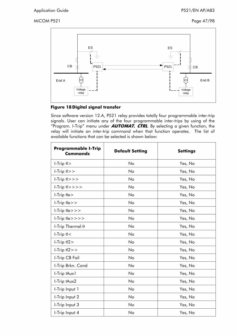
Application Guide P521/EN AP/A83 MiCOM P521 Page 47/98
CB
ES
End A End B
CB
ES
P521 P521
Voltage relay
Voltage relay
Figure 18 Digital signal transfer
Since software version 12.A, P521 relay provides totally four programmable inter-trip signals. User can initiate any of the four programmable inter-trips by using of the “Program. I-Trip” menu under AUTOMAT. CTRL. By selecting a given function, the relay will initiate an inter-trip command when that function operates. The list of available functions that can be selected is shown below:
Programmable I-Trip Commands
Default Setting Settings
I-Trip tI> No Yes, No
I-Trip tI>> No Yes, No
I-Trip tI>>> No Yes, No
I-Trip tI>>>> No Yes, No
I-Trip tIe> No Yes, No
I-Trip tIe>> No Yes, No
I-Trip tIe>>> No Yes, No
I-Trip tIe>>>> No Yes, No
I-Trip Thermal θ No Yes, No
I-Trip tI< No Yes, No
I-Trip tI2> No Yes, No
I-Trip tI2>> No Yes, No
I-Trip CB Fail No Yes, No
I-Trip Brkn. Cond No Yes, No
I-Trip tAux1 No Yes, No
I-Trip tAux2 No Yes, No
I-Trip Input 1 No Yes, No
I-Trip Input 2 No Yes, No
I-Trip Input 3 No Yes, No
I-Trip Input 4 No Yes, No
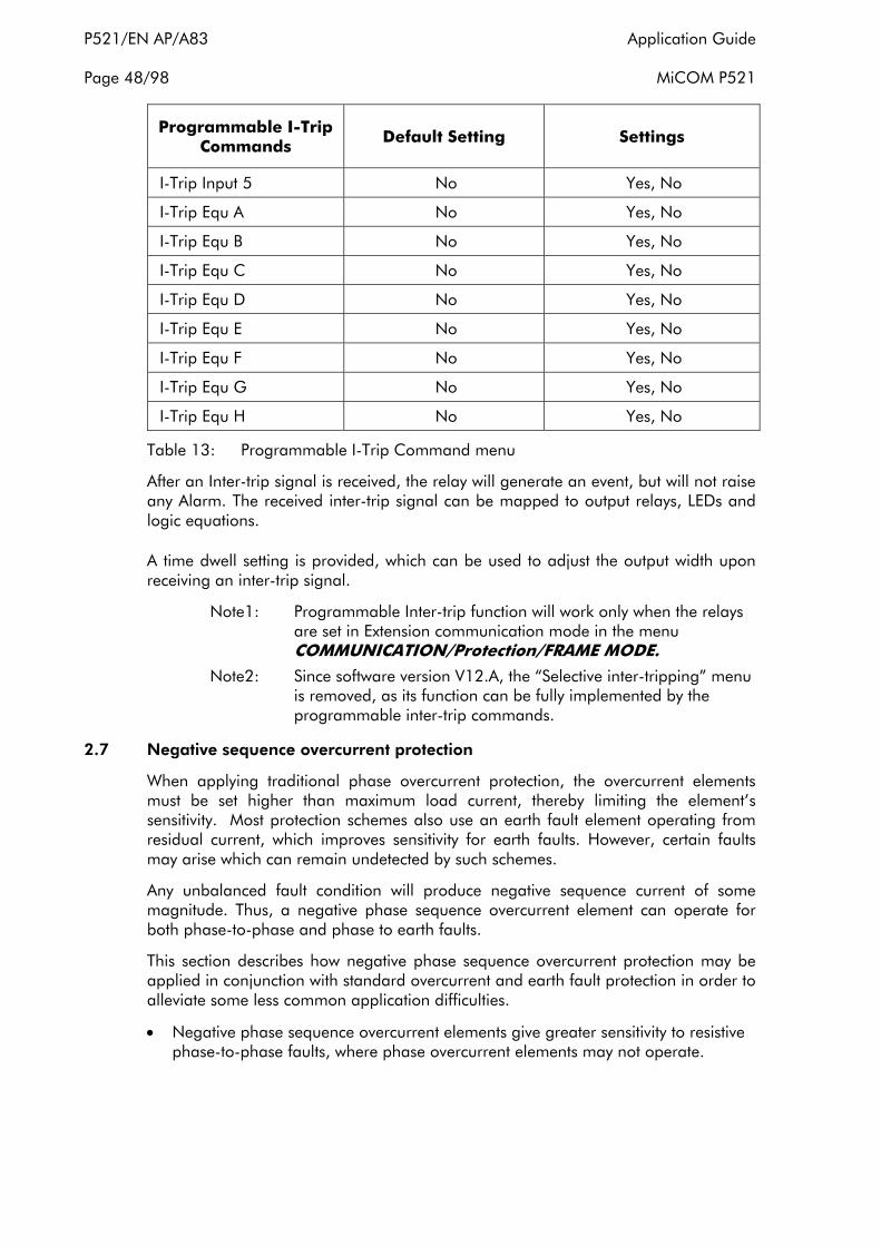
P521/EN AP/A83 Application Guide Page 48/98 MiCOM P521
Programmable I-Trip Commands
Default Setting Settings
I-Trip Input 5 No Yes, No
I-Trip Equ A No Yes, No
I-Trip Equ B No Yes, No
I-Trip Equ C No Yes, No
I-Trip Equ D No Yes, No
I-Trip Equ E No Yes, No
I-Trip Equ F No Yes, No
I-Trip Equ G No Yes, No
I-Trip Equ H No Yes, No
Table 13: Programmable I-Trip Command menu
After an Inter-trip signal is received, the relay will generate an event, but will not raise any Alarm. The received inter-trip signal can be mapped to output relays, LEDs and logic equations.
A time dwell setting is provided, which can be used to adjust the output width upon receiving an inter-trip signal.
Note1: Programmable Inter-trip function will work only when the relays are set in Extension communication mode in the menu COMMUNICATION/Protection/FRAME MODE.
Note2: Since software version V12.A, the “Selective inter-tripping” menu is removed, as its function can be fully implemented by the programmable inter-trip commands.
2.7 Negative sequence overcurrent protection
When applying traditional phase overcurrent protection, the overcurrent elements must be set higher than maximum load current, thereby limiting the element’s sensitivity. Most protection schemes also use an earth fault element operating from residual current, which improves sensitivity for earth faults. However, certain faults may arise which can remain undetected by such schemes.
Any unbalanced fault condition will produce negative sequence current of some magnitude. Thus, a negative phase sequence overcurrent element can operate for both phase-to-phase and phase to earth faults.
This section describes how negative phase sequence overcurrent protection may be applied in conjunction with standard overcurrent and earth fault protection in order to alleviate some less common application difficulties.
• Negative phase sequence overcurrent elements give greater sensitivity to resistive phase-to-phase faults, where phase overcurrent elements may not operate.

Application Guide P521/EN AP/A83 MiCOM P521 Page 49/98
• In certain applications, residual current may not be detected by an earth fault relay due to the system configuration. For example, an earth fault relay applied on the delta side of a delta-star transformer is unable to detect earth faults on the star side. However, negative sequence current will be present on both sides of the transformer for any fault condition, irrespective of the transformer configuration. Therefore, a negative phase sequence overcurrent element may be employed to provide time-delayed back-up protection for any un-cleared asymmetrical faults.
• Where rotating machines are protected by fuses, a blown fuse produces a large amount of negative sequence current. This is a dangerous condition for the machine due to the heating effects of negative phase sequence current at double frequency. A negative phase sequence overcurrent element may be applied to provide efficient back-up protection for dedicated motor protection relays.
• It may also be required to simply alarm for the presence of negative phase sequence currents on the system. Operators are then prompted to investigate the cause of the unbalance.
The negative phase sequence overcurrent element has a current pick up setting ‘Ι2>’, and is time delayed in operation by the adjustable timer ‘tΙ2> Delay Time.’
2.7.1 Ι2> and Ι2>> setting guidelines
The current pick-up threshold (PROTECTION G1 (G2)/[46] Neg Seq OC menu) must be set higher than the normal negative phase sequence current due to the normal load unbalance on the system. This can be set at the commissioning stage, making use of the relay measurement function to display the standing negative phase sequence current, and apply a setting at least 20% above this figure.
Where the negative phase sequence element is required to operate for specific un-cleared asymmetric faults, a precise threshold setting has to be based on an individual fault analysis for that particular system due to the complexities involved. However, to ensure operation of the protection, the current pick-up setting must be set approximately 20% below the lowest calculated negative phase sequence fault current for a specific remote fault condition.
The correct setting of the time delay for this function is vital. It should also be noted that this element is applied primarily to provide back-up protection to other protective devices or to provide an alarm. Therefore, it would be associated with a long time delay.
It must be ensured that the time delay is set greater than the operating time of any other protective device (at minimum fault level) on the system which may respond to unbalanced faults, such as:
• Phase overcurrent elements
• Earth fault elements
• Broken conductor elements
• Negative phase sequence influenced thermal elements
The Ι2> element can be set to either DMT, IDMT, RI inverse or definite time delay in the “Ι2> Delay Type” cell. The Ι2>> threshold is definite time only. The Ι2 settings are located in the PROTECTION G1 (G2)/[46] Neg Seq OC menu. The time multiplier setting, time dial, curve selection and reset time, associated with the Ι2> threshold, are set in much the same way as the [50] phase overcurrent menu.

P521/EN AP/A83 Application Guide Page 50/98 MiCOM P521
The settings associated with the negative sequence overcurrent protection are shown in table 14 below:
[46] Neg Seq OC
Default Setting
Min Max Step
Ι2> ? No Yes, No
Ι2> 1 Ιn 0.1 Ιn 40 Ιn 0.01 Ιn
Ι2> Delay Type DMT DMT, IDMT, RI
tΙ2> 0 ms 0 s 150 s 0.01 s
Ι2> Curve IEC SΙ IEC STI, IEC SI, IEC VI, IEC EI, IEC LTI, CO2,
IEEE MI, CO8, IEEE VI, IEEE EI
Ι2> Tms 1 0.025 1.5 0.025
Ι2> Time Dial 0.1 0.1 100 0.1
K 0.1 0.1 10 0.005
Reset Type DMT DMT IDMT N/A
tReset 40 ms 40 ms 100 s 0.01 s
Rtms 0.025 0.025 3.2 0.025
Ι2>> ? No Yes, No
Ι2>> 1 Ιn 0.1 Ιn 40 Ιn 0.01 Ιn
tΙ2>> 0 ms 0 s 150 s 0.01 s
Table 14: Negative sequence overcurrent settings
2.8 Undercurrent protection function
The MiCOM P521 relay includes 2 undercurrent elements, one of which is dedicated to the CB fail detection (see CB failure protection section). Another undercurrent element is provided as a protection function to detect loss of load conditions.
1, %
+-./)
10 !4
8
8
8
8 0-
Figure 19 Undercurrent protection logic

Application Guide P521/EN AP/A83 MiCOM P521 Page 51/98
The undercurrent protection function is available only if the 52a auxiliary contact, indicating the CB status, is connected to one of the 5 logic inputs in the relay. The chosen logic input should be energized via the 52a contact of the circuit breaker.
To allocate a logic input to the 52a auxiliary contact, ‘52a’ must be selected in the following location:
− AUTOMAT. CTRL/Inputs/Input #/ 52a
An “Ι<” alarm is given when at least one of the 3 phase current falls below the Ι< threshold and the CB is closed (indicated by the 52a input). When the alarm condition has been present for longer than the set time tΙ<, one or more output relays can be energized.
See the AUTOMAT. CTRL/Trip Commands/ Trip tΙ< menu for the allocation of tΙ< to the trip output relay RL1.
See the AUTOMAT. CTRL/Output Relays/ tΙ< menu for the allocation of tΙ< to the auxiliary output relays RL2 to RL8.
Table 15 below shows the undercurrent protection settings:
[37] Undercurrent
Default Setting
Min Max Step
Ι< ? No Yes, No
Ι< 0.2 Ιn 0.02 Ιn 1 Ιn 0.01 Ιn
tΙ< 0 ms 0 s 150 s 0.01 s
Table 15: Undercurrent protection settings
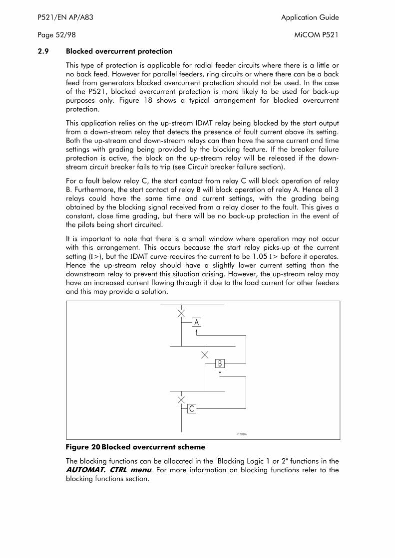
P521/EN AP/A83 Application Guide Page 52/98 MiCOM P521
2.9 Blocked overcurrent protection
This type of protection is applicable for radial feeder circuits where there is a little or no back feed. However for parallel feeders, ring circuits or where there can be a back feed from generators blocked overcurrent protection should not be used. In the case of the P521, blocked overcurrent protection is more likely to be used for back-up purposes only. Figure 18 shows a typical arrangement for blocked overcurrent protection.
This application relies on the up-stream IDMT relay being blocked by the start output from a down-stream relay that detects the presence of fault current above its setting. Both the up-stream and down-stream relays can then have the same current and time settings with grading being provided by the blocking feature. If the breaker failure protection is active, the block on the up-stream relay will be released if the down-stream circuit breaker fails to trip (see Circuit breaker failure section).
For a fault below relay C, the start contact from relay C will block operation of relay B. Furthermore, the start contact of relay B will block operation of relay A. Hence all 3 relays could have the same time and current settings, with the grading being obtained by the blocking signal received from a relay closer to the fault. This gives a constant, close time grading, but there will be no back-up protection in the event of the pilots being short circuited.
It is important to note that there is a small window where operation may not occur with this arrangement. This occurs because the start relay picks-up at the current setting (Ι>), but the ΙDMT curve requires the current to be 1.05 Ι> before it operates. Hence the up-stream relay should have a slightly lower current setting than the downstream relay to prevent this situation arising. However, the up-stream relay may have an increased current flowing through it due to the load current for other feeders and this may provide a solution.
%
Figure 20 Blocked overcurrent scheme
The blocking functions can be allocated in the "Blocking Logic 1 or 2" functions in the AUTOMAT. CTRL menu. For more information on blocking functions refer to the blocking functions section.

Application Guide P521/EN AP/A83 MiCOM P521 Page 53/98
2.10 Selective scheme logic
The blocked overcurrent protection section describes the use of non-cascade protection schemes which use the start contacts from downstream relays to block operation of upstream relays. In the case of Selective Overcurrent Logic (SOL), the start contacts are used to temporarily increase the time delays of upstream relays, instead of blocking them. This provides an alternative approach to achieving a non-cascade type of overcurrent scheme. It may be more familiar to some utilities than the blocked overcurrent arrangement.
%
Figure 21 Typical scheme logic
The SOL function temporarily changes the time delay settings of the second, third and fourth stages of phase overcurrent and earth fault elements (Ι>>, Ι>>>, Ι>>>>, Ιe>>, Ιe>>> and Ιe>>>>) to the tSel1 or tSel2 timer settings. The choice of timers will depend upon which selective logic function is enabled, either Log Sel1 or Log Sel 2. The Log Sel1 or Log Sel2 functions are enabled by selecting, then energizing, one of the 5 opto inputs (AUTOMAT.CTRL/Inputs/Input #).
The Logic Select 1 settings (AUTOMAT. CTRL) are shown in the table 16 below. These settings are identical to the Logic Select 2 menu.
Logic Select. 1 (2) Default Setting
Min Max Step
Sel1 tΙ>> No Yes, No
Sel1 tΙ>>> No Yes, No
Sel1 tΙ>>>> No Yes, No
Sel1 tΙe>> No Yes, No
Sel1 tΙe>>> No Yes, No
Sel1 tΙe>>>> No Yes, No
tsel1 0 ms 0 s 150 s 0.01 s
Table 16: Selective logic settings
Note: Choosing ‘Yes’ selects the function to modified by the Logic Select function.
P521/EN AP/A83 Application Guide Page 54/98 MiCOM P521
To allow time for a start contact to initiate a change of setting, the time settings of the second, third and fourth stages should include a nominal delay. Guidelines for minimum time settings are identical to those given for blocked overcurrent schemes.
2.11 Cold load pick-up
The cold load pickup feature enables the selected settings of the MiCOM P521 relay to be changed to cater for temporary overload conditions that may occur during cold starts, such as switching on large heating loads after a sufficient cooling period, or loads that draw high initial starting currents.
When a feeder is energized, the current levels for a period of time following energization may differ greatly from the normal load levels. Although this will not affect the current differential protection, the back-up overcurrent settings that have been applied may not be suitable during this period.
The Cold Load Pick-Up (CLP) logic serves to raise the settings of selected stages for a selectable duration. This allows the protection settings to be set closer to the load profile by automatically increasing them after energization. The CLP logic provides stability, without compromising protection performance during starting. Note that any of the disabled overcurrent stages in the main relay menu will not appear in the Cold Load PU Menu.
Table 17 below shows the relay menu for the ‘Cold Load Pick-up’ logic, including the available setting ranges and factory defaults.
Cold Load PU Default Setting
Min Max Step
Cold Load PU ? No Yes, No
tΙ>? No Yes, No
tΙ>>? No Yes, No
tΙ>>>? No Yes, No
tΙ>>>>? No Yes, No
tΙe>? No Yes, No
tΙe>>? No Yes, No
tΙe>>>? No Yes, No
tΙe>>>> No Yes, No
tΙ2>? No Yes, No
tΙ2>>? No Yes, No
tTherm? No Yes, No
Level 50% 20% 500% 1%
tCL 1 s 0.1 s 3600 s 0.1 s
Table 17: Cold load pick-up settings
The tCL timer controls the time for which the relevant overcurrent and earth fault settings are altered following an external input (e.g. circuit breaker closure). When the set tCL time has elapsed, all of the relevant settings revert back to their original values. The tCL timer is initiated via a dedicated logic input (refer to AUTOMAT. CTRL/Inputs/Input #/ Cold L PU) signal generated by connecting an auxiliary contact from the circuit breaker or starting device to the relay’s opto-inputs.

Application Guide P521/EN AP/A83 MiCOM P521 Page 55/98
The Level setting indicates by what percentage the current thresholds are modified. For example, a 0.8 A setting will be increased to 1.6 A if the Level setting is 200%.
The following sections describe applications where the CLP logic may be useful and the settings that need to be applied.
2.11.1 Air conditioning/resistive heating loads
Where a feeder is used to supply air conditioning or resistive heating loads there may be a conflict between the ‘steady state’ overcurrent settings and those required following energization. This is due to the temporary increase in load current that may arise during starting. The CLP logic is used to alter the applied settings during this time.
With the Cold Load PU enabled, the affected thresholds are selected to be adjusted for the required time to allow the start condition to subside. A percentage value is selected as the amount by which the selected threshold is increased/decreased.
The time for which the adjusted thresholds are valid is defined by the tCL setting. After this time, the settings return to normal.
It may not be necessary to alter the protection settings following a short supply interruption. In this case the CLP function is not activated.
2.11.2 Motor feeders
In general, feeders supplying motor loads would be protected by a dedicated motor protection device, such as the MiCOM P220 or P241 relay. However, if no specific protection has been applied (possibly due to economic reasons) then the CLP function in the MiCOM P521 relay may be used to modify the overcurrent settings accordingly during starting.
Depending upon the magnitude and duration of the motor starting current, it may be sufficient to simply block operation of instantaneous elements or, if the start duration is long, the time delayed protection settings may also need to be raised. Hence, a combination of both blocking and raising of settings of the relevant overcurrent stages may be adopted. The CLP overcurrent settings in this case must be chosen with regard to the motor starting characteristic.
As previously described, the CLP logic includes the option of raising the current settings of the overcurrent and earth fault protection. This may be useful where instantaneous earth fault protection needs to be applied to the motor. During conditions of motor starting, it is likely that incorrect operation of the earth fault element would occur due to asymmetric CT saturation. This is a result of the high level of starting current causing saturation of one or more of the line CT’s feeding the overcurrent/earth fault protection. The resultant transient imbalance in the secondary line current quantities is thus detected by the residually connected earth fault element. For this reason, it is normal to either apply a nominal time delay to the element, or to utilize a series stabilizing resistor.
The CLP logic may be used to allow reduced operating times or current settings to be applied to the earth fault element under normal running conditions. These settings could then be raised prior to motor starting, via the logic.

P521/EN AP/A83 Application Guide Page 56/98 MiCOM P521
2.11.3 Earth fault protection applied to transformers
Where an earth fault relay is residually connected on the primary side of a delta-star transformer, no time delay is required for co-ordination purposes, due to the presence of the delta winding. However, a nominal time delay or stabilizing resistor is recommended to ensure transient stability during transformer energization.
The CLP logic may be used in a similar manner to that previously described for the motor application.
It should be noted that this method will not provide stability in the event of asymmetric CT saturation which occurs as a result of an unbalanced fault condition. If problems of this nature are encountered, the best solution would still be the use of a stabilizing resistor.
2.11.4 Switch onto fault protection (SOTF)
In some feeder applications, fast tripping may be required if a fault is present on the feeder when it is energized.
Such faults may be due to a fault condition not having been removed from the feeder, or due to earthing clamps having been left on following maintenance. In either case, it may be desirable to clear the fault condition in an accelerated time, rather than waiting for the time delay associated with ΙDMT overcurrent protection.
The above situation may be catered for by the CLP logic. Selected overcurrent/earth fault stages could be set to a lower threshold (typically 30% of the nominal threshold) for a defined period following circuit breaker closure (typically 200 ms). Hence, fault clearance would be achieved for a switch onto fault (SOTF) condition.

Application Guide P521/EN AP/A83 MiCOM P521 Page 57/98
3. APPLICATION OF NON-PROTECTION FUNCTIONS
3.1 Auxiliary timers (tAux 1 and tAux 2)
Two auxiliary timers tAux1 and tAux2 are available associated to Aux1 and Aux2 logic inputs (refer to AUTOMAT.CRTL/INPUTS menu). When these inputs are energized, the associated timers start and after the set time, the output relays close (refer to AUTOMAT.CRTL/OUTPUTS menu). The time delays are independently settable from 0 ms to 200 s. The timer settings tAux1 and tAux2 can be found under AUTOMAT.CRTL/INPUTS/Aux1 Time (or Aux2 Time).
3.2 Setting group selection
The MiCOM P521 relay has two setting groups related to the protection functions named PROTECTION G1 and PROTECTION G2. Only one group is active at any one time. Changes between the two groups are done via the front interface (CONFIGURATION/Group Select/Setting Group 1 or 2), a dedicated logic input (AUTOMAT CTRL/Inputs/Input #/Changeset) where # is the chosen logic input or through the communication ports (refer to Communication Mapping Guide P521/EN GC for more detailed information).
The relative priority of the different ways of changing the active setting group is listed below:
ORIGIN OF THE ORDER PRIORITY LEVEL
FRONT PANEL HIGHEST
LOGIC INPUT MEDIUM
REMOTE COMMUNICATION LOWEST
To avoid nuisance tripping the setting group change is only executed when no protection function (except for current differential and thermal overload functions) or automation function is running. If a setting group change is received during any protection or automation function it is stored and executed after the last protection timer has elapsed.
The active group is displayed in the OP PARAMETERS menu.
The active group can also be assigned to an output relay by selecting “Active Group” in AUTOMAT. CTRL/Output relays. If a normally open contact is chosen:
− an open contact will indicate Group 1
− a closed contact will indicate Group 2
P521/EN AP/A83 Application Guide Page 58/98 MiCOM P521
3.2.1 Change of setting group by a logic input
It is possible to configure how the digital inputs are activated, either on a falling edge/ low level or on a rising edge/ high level. The choice is made in the CONFIGURATION/Configuration Inputs/Inputs menu (0=falling edge/ low level, 1=rising edge/ high level). The setting group input mode (EDGE or LEVEL) can be selected in the CONFIGURATION/Group Select/Change Group Input menu.
3.2.2 Manual setting group change via front interface
The setting group can be selected to be 1 or 2 in the CONFIGURATION/Group Select/Setting group menu. Manual changes can only be made if “EDGE” is selected in the “Change Group Input” cell.
3.3 Latch functions
Following a protection trip the trip contact (RL1) remains closed until the current falls below the undercurrent threshold or for the “tOpen Pulse” time (AUTOMAT. CTRL/CB Supervision menu), whichever is the greater. Some applications, however, demand that the trip contact must latch following a protection trip. The MiCOM P521 caters for this requirement by allowing the user to latch RL1 after being operated by one or several thresholds. This means, for example, that RL1 can be latched for a current differential trip, but could be selected not to latch for an overcurrent trip. Table 18 below shows the “Latch Functions” menu; to latch a given function, following a trip, select “Yes”. Selecting “No” means that the function will not be latched.
The “Latch Functions” menu can be found under AUTOMAT. CTRL.
Latch Functions Default Setting Choices
Latch Ιdiff No Yes, No
Latch Direct I-Trip No Yes, No
Latch C Diff I-Trip No Yes, No
Latch PIT No Yes, No
Latch tΙ> No Yes, No
Latch tΙ>> No Yes, No
Latch tΙ>>> No Yes, No
Latch tΙ>>>> No Yes, No
Latch tΙe> No Yes, No
Latch tΙe>> No Yes, No
Latch tΙe>>> No Yes, No
Latch tΙe>>>> No Yes, No
Latch tΙ< No Yes, No
Latch tΙ2> No Yes, No
Latch tΙ2>> No Yes, No
Latch Thermal θ No Yes, No
Latch Brkn. Cond No Yes, No

Application Guide P521/EN AP/A83 MiCOM P521 Page 59/98
Latch Functions Default Setting Choices
Latch t Aux 1 No Yes, No
Latch t Aux 2 No Yes, No
Table 18: Latch functions menu
The latched RL1 contact can be reset by reading ( ) and clearing (C) the relevant protection alarm.
3.4 Blocking functions
The P521 allows the user to block operation of any protection function by energizing a selected digital input. To block operation of a protection function the user must first select the function to be blocked, followed by a digital input to perform the block.
The Blocking Logic 1 and Blocking Logic 2 (AUTOMAT. CTRL) contain a list of protection functions that can be blocked. Selecting ‘Yes’ adds the chosen function to the list of functions that will be blocked when the appropriate input is energized. Table 19 below shows a list of the protection functions available in the Blocking Logic 1 and Blocking Logic 2 menus.
Blocking Logic 1 (2) Default Setting Choices
Block Ιdiff No Yes, No
Block tΙ> No Yes, No
Block tΙ>> No Yes, No
Block tΙ>>> No Yes, No
Block tΙ>>>> No Yes, No
Block tΙe> No Yes, No
Block tΙe>> No Yes, No
Block tΙe>>> No Yes, No
Block tΙe>>>> No Yes, No
Block tΙ2> No Yes, No
Block tΙ2>> No Yes, No
Block Therm θ No Yes, No
Block Brkn. Cond No Yes, No
Block t Aux 1 No Yes, No
Block t Aux 2 No Yes, No
Table 19: Blocking logic menu
Energizing the chosen digital input will block every protection function that has been selected. To perform the blocking function the digital input must be allocated to either Blk Log 1 or Blk Log 2.
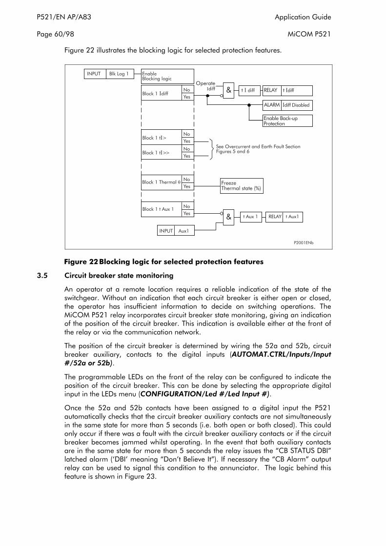
P521/EN AP/A83 Application Guide Page 60/98 MiCOM P521
Figure 22 illustrates the blocking logic for selected protection features.
( )& )
)$$*
) +*
) ++*
,-
$$ $$ .&%*
$$
%&%./ $$0
)12
3-42 "2 3 2'
)" *
) %25 *
6" 789
, %25 .&%* %25
(%25
Figure 22 Blocking logic for selected protection features
3.5 Circuit breaker state monitoring
An operator at a remote location requires a reliable indication of the state of the switchgear. Without an indication that each circuit breaker is either open or closed, the operator has insufficient information to decide on switching operations. The MiCOM P521 relay incorporates circuit breaker state monitoring, giving an indication of the position of the circuit breaker. This indication is available either at the front of the relay or via the communication network.
The position of the circuit breaker is determined by wiring the 52a and 52b, circuit breaker auxiliary, contacts to the digital inputs (AUTOMAT.CTRL/Inputs/Input #/52a or 52b).
The programmable LEDs on the front of the relay can be configured to indicate the position of the circuit breaker. This can be done by selecting the appropriate digital input in the LEDs menu (CONFIGURATION/Led #/Led Input #).
Once the 52a and 52b contacts have been assigned to a digital input the P521 automatically checks that the circuit breaker auxiliary contacts are not simultaneously in the same state for more than 5 seconds (i.e. both open or both closed). This could only occur if there was a fault with the circuit breaker auxiliary contacts or if the circuit breaker becomes jammed whilst operating. In the event that both auxiliary contacts are in the same state for more than 5 seconds the relay issues the “CB STATUS DBI” latched alarm (‘DBI’ meaning “Don’t Believe It”). If necessary the “CB Alarm” output relay can be used to signal this condition to the annunciator. The logic behind this feature is shown in Figure 23.

Application Guide P521/EN AP/A83 MiCOM P521 Page 61/98
&) *(
&) *(
DD
*("
+$ *2((*2&
+, *+$
D
00
00
00
''
Figure 23 CB Status DBI logic diagram
3.6 CB control
The P521 allows the circuit breaker to be manually tripped or closed by any one of the following three methods:
1. Via user interface
2. Via opto inputs
3. Via control communications (SCADA etc.)
Methods 1 and 2 are explained below. Method 3, via control communications, is clearly described in the P521 communication mapping guide (P521/EN GC).
If an attempt to close the breaker is being made, and a protection trip signal is generated, the protection trip command overrides the close command.
3.6.1 CB trip and close via user interface
To manually trip or close the circuit breaker via the user interface the user must first locate the “Trip and Close” cell in the OP PARAMETERS menu. Pressing the key in this cell, followed by or will display either “Trip”, “Close” or “No Operation”. If “No Operation” is selected a CB trip or close will not be performed. Selecting “Trip” will cause the trip contact (RL1) to operate for a duration equal to the “t Open Pulse” time (AUTOMAT. CTRL/CB Supervision). The operation will be accompanied by the illumination of the Trip LED and the “REM TRIP” alarm (indicating a remote trip has been performed). An event and fault record will be generated every time a remote trip is performed.
If “Close” is selected in the “Trip and Close” cell the relay closes the output contact assigned to “CB Close” for a duration equal o the “t Close Pulse” time. The “CB Close” command will also generate a protection event.

P521/EN AP/A83 Application Guide Page 62/98 MiCOM P521
3.6.2 CB trip and close via opto inputs
If necessary the circuit breaker can be tripped or closed by energizing the appropriate opto input. To assign an opto to either of these functions the user must select either “Log Trip” or “Log Close” in the inputs column (AUTOMAT. CTRL). Energizing the Log Trip input will cause the trip contact to operation for a duration equal to the “t Trip Pulse” time + the total time the opto input is energized. The operation will be accompanied by the TRIP LED illuminating and the “REM TRIP” alarm being displayed. An event and fault record will be generated every time a remote trip is performed.
Energizing the “Log Close” input causes the contact assigned to “CB Close” to operate for a duration equal to “t Close Pulse” time + the total time the opto input is energized. Closing the breaker via an opto input will also generate a protection event.
3.6.3 CB manual trip and close delays
The P521 relay also offers the facility of delaying the manual trip or close operation. This would give personnel time to move away from the circuit breaker following a trip or close command. The associated delays are set using the “CB Man Trip Dly” and “CB Man Close Dly” settings (AUTOMAT. CTRL/CB Supervision). Once a manual trip or close has been initiated the relay displays either “Tripping” or “Closing” for the duration of the selected delays. Pressing the key, while either of the messages are being displayed, will cancel the operation. The manual delay time will apply to all manual CB trip or close commands from any interface (keypad, opto input, front port or rear port).
3.7 Circuit breaker condition monitoring
Periodic maintenance of circuit breakers is necessary to ensure that the trip circuit mechanism operates correctly and also that the interrupting capability has not been compromised due to previous fault interruptions. Generally such maintenance is based on a fixed time interval or a fixed number of fault current interruptions. These methods of monitoring circuit breaker condition give a rough guide only and can lead to excessive maintenance.
The relay records various statistics related to each circuit breaker trip operation, allowing a more accurate assessment of the circuit breaker condition to be determined. These monitoring features are discussed in the following section.
3.7.1 Circuit breaker condition monitoring features
For each circuit breaker trip operation the relay records statistics as shown in the following table, taken from the relay menu. The RECORDS/CB Monitoring menu cells shown, are counter values only. In the event that any of the counters exceed a settable threshold (explained later), an output contact or LED can be operated (both labeled “CB Alarm”). In addition to operating an LED or contact, the relay will also display an alarm message, on the LCD, which is unique to each monitoring feature.
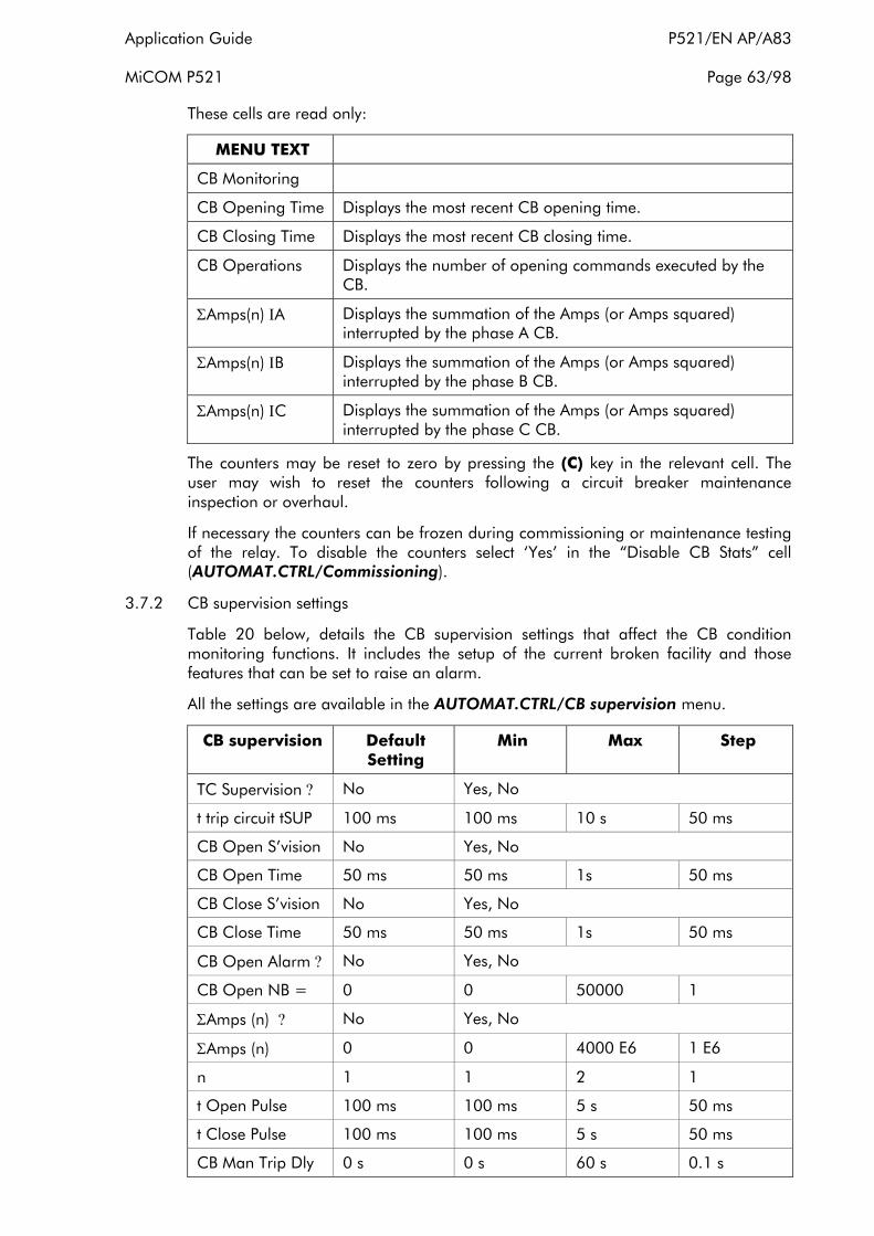
Application Guide P521/EN AP/A83 MiCOM P521 Page 63/98
These cells are read only:
MENU TEXT
CB Monitoring
CB Opening Time Displays the most recent CB opening time.
CB Closing Time Displays the most recent CB closing time.
CB Operations Displays the number of opening commands executed by the CB.
ΣAmps(n) ΙA Displays the summation of the Amps (or Amps squared) interrupted by the phase A CB.
ΣAmps(n) ΙB Displays the summation of the Amps (or Amps squared) interrupted by the phase B CB.
ΣAmps(n) ΙC Displays the summation of the Amps (or Amps squared) interrupted by the phase C CB.
The counters may be reset to zero by pressing the (C) key in the relevant cell. The user may wish to reset the counters following a circuit breaker maintenance inspection or overhaul.
If necessary the counters can be frozen during commissioning or maintenance testing of the relay. To disable the counters select ‘Yes’ in the “Disable CB Stats” cell (AUTOMAT.CTRL/Commissioning).
3.7.2 CB supervision settings
Table 20 below, details the CB supervision settings that affect the CB condition monitoring functions. It includes the setup of the current broken facility and those features that can be set to raise an alarm.
All the settings are available in the AUTOMAT.CTRL/CB supervision menu.
CB supervision Default Setting
Min Max Step
TC Supervision ? No Yes, No
t trip circuit tSUP 100 ms 100 ms 10 s 50 ms
CB Open S’vision No Yes, No
CB Open Time 50 ms 50 ms 1s 50 ms
CB Close S’vision No Yes, No
CB Close Time 50 ms 50 ms 1s 50 ms
CB Open Alarm ? No Yes, No
CB Open NB = 0 0 50000 1
ΣAmps (n) ? No Yes, No
ΣAmps (n) 0 0 4000 E6 1 E6
n 1 1 2 1
t Open Pulse 100 ms 100 ms 5 s 50 ms
t Close Pulse 100 ms 100 ms 5 s 50 ms
CB Man Trip Dly 0 s 0 s 60 s 0.1 s
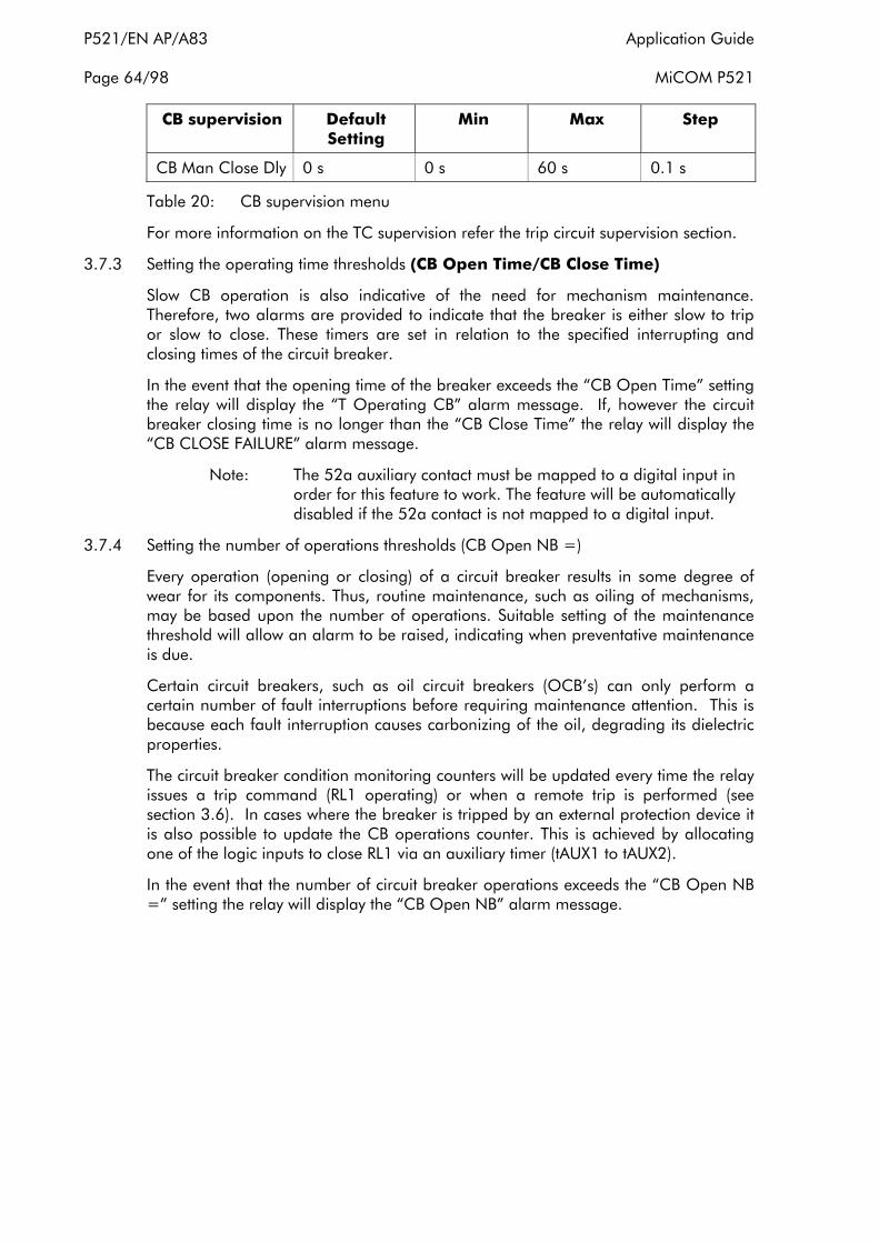
P521/EN AP/A83 Application Guide Page 64/98 MiCOM P521
CB supervision Default Setting
Min Max Step
CB Man Close Dly 0 s 0 s 60 s 0.1 s
Table 20: CB supervision menu
For more information on the TC supervision refer the trip circuit supervision section.
3.7.3 Setting the operating time thresholds (CB Open Time/CB Close Time)
Slow CB operation is also indicative of the need for mechanism maintenance. Therefore, two alarms are provided to indicate that the breaker is either slow to trip or slow to close. These timers are set in relation to the specified interrupting and closing times of the circuit breaker.
In the event that the opening time of the breaker exceeds the “CB Open Time” setting the relay will display the “T Operating CB” alarm message. If, however the circuit breaker closing time is no longer than the “CB Close Time” the relay will display the “CB CLOSE FAILURE” alarm message.
Note: The 52a auxiliary contact must be mapped to a digital input in order for this feature to work. The feature will be automatically disabled if the 52a contact is not mapped to a digital input.
3.7.4 Setting the number of operations thresholds (CB Open NB =)
Every operation (opening or closing) of a circuit breaker results in some degree of wear for its components. Thus, routine maintenance, such as oiling of mechanisms, may be based upon the number of operations. Suitable setting of the maintenance threshold will allow an alarm to be raised, indicating when preventative maintenance is due.
Certain circuit breakers, such as oil circuit breakers (OCB’s) can only perform a certain number of fault interruptions before requiring maintenance attention. This is because each fault interruption causes carbonizing of the oil, degrading its dielectric properties.
The circuit breaker condition monitoring counters will be updated every time the relay issues a trip command (RL1 operating) or when a remote trip is performed (see section 3.6). In cases where the breaker is tripped by an external protection device it is also possible to update the CB operations counter. This is achieved by allocating one of the logic inputs to close RL1 via an auxiliary timer (tAUX1 to tAUX2).
In the event that the number of circuit breaker operations exceeds the “CB Open NB =” setting the relay will display the “CB Open NB” alarm message.

Application Guide P521/EN AP/A83 MiCOM P521 Page 65/98
3.7.5 Setting the Σ Ιn thresholds (Σ Amps (n))
Where overhead lines are prone to frequent faults and are protected by oil circuit breakers (OCB’s), oil changes account for a large proportion of the life cycle cost of the switchgear. Generally, oil changes are performed at a fixed interval of circuit breaker fault operations. However, this may result in premature maintenance where fault currents tend to be low, and hence oil degradation is slower than expected.
The Σ Ιn counter monitors the cumulative severity of the duty placed on the interrupter, allowing a more accurate assessment of the circuit breaker condition to be made.
For OCB’s, the dielectric withstand of the oil generally decreases as a function of Σ Ι2t. This is where ‘Ι’ is the fault current broken, and ‘t’ is the arcing time within the interrupter tank (not the interrupting time). As the arcing time cannot be determined accurately, the relay would normally be set to monitor the sum of the broken current squared, by setting n = 2.
For other types of circuit breaker, especially those operating on higher voltage systems, practical evidence suggests that the value of n = 2 may be inappropriate. In such applications n may be set to 1.
An alarm in this instance may be indicative of the need for gas/vacuum interrupter HV pressure testing, for example.
It is imperative that any maintenance programme must be fully compliant with the switchgear manufacturer’s instructions.
The P521 relay records the fault current at the instant the trip output (RL1) is initiated. This current is then summed with the value previously recorded. If the summed current exceeds the “Σ Amps (n)” threshold the relay will display the “Sum A n” alarm message.
In cases where the circuit breaker is tripped by an external protection device it is also possible to update the ΣΙn counter. This is achieved by allocating one of the logic inputs to close RL1 via an auxiliary timer (tAUX1 and tAUX2).
3.7.6 Setting the trip and close pulse times (t Open Pulse/t Close Pulse)
The length of the trip or close pulse can be set via the ‘t Open Pulse’ and ‘t Close Pulse’ settings respectively. These should be set long enough to ensure the breaker has completed its open or close cycle before the pulse has elapsed.
The duration of the opening time is measured from the trip pulse being issued to the opening of the 52a auxiliary contact. Conversely, the duration of the closing time is measured from the close pulse being issued to the 52a closing.
3.8 Trip circuit supervision
The trip circuit extends beyond the relay enclosure and passes through more components, such as fuse, links, relay contacts, auxiliary contacts and so on. These complications, coupled with the importance of the circuit, have directed attention to its supervision.

P521/EN AP/A83 Application Guide Page 66/98 MiCOM P521
3.8.1 MiCOM P521 trip circuit supervision mechanism
The Trip Circuit Supervision function included in the MiCOM P521 relay is performed as follows:
A logic input can be assigned in the AUTOMAT.CTRL/Inputs/ Input #/Trip Circ menu cell. This logic input must be inserted in the trip circuit according to one of the typical application diagrams, shown later.
When the function TC Supervision is enabled by selecting ‘Yes’ within the AUTOMAT.CTRL/CB Supervision sub-menu, the relay continuously checks the trip circuit continuity whatever the CB status – opened CB or closed CB. This function is enabled when the trip output contact (relay RL1) is not energized and it is disabled as long as the trip output contact is operating.
A “TRIP CIRCUIT” alarm signal (trip circuit failure) is generated if the opto-input detects no voltage signal for a time longer than the settable timer tSUP (AUTOMAT.CTRL/CB Supervision). The “52 Fail” contact can be selectively closed in the event of a trip coil failure.
As the TC supervision function is disabled when the trip output contact is operating, this function is suitable for use with the product latching logic on.
The TC supervision function can be selectively blocked from an external trip contact, so that any external trip (not using the P521 to trip the CB) can be used, without the P521 giving the “TRIP CIRCUIT” alarm. The external trip contact is wired into a logic input, which is assigned in the AUTOMAT.CTRL/Inputs/ Input #/TCS Block menu cell.
The following table shows the setting associated with the trip circuit supervision function:
Setting Range Menu
Min Max Step
TC Supervision ? Yes No
tSUP 100 ms 10 s 50 ms
& 2
. : 6
,
3
Figure 24 Trip circuit supervision logic diagram
Three application examples are shown below.
Example 1
In this example only the 52a auxiliary contact is available, the MiCOM P521 relay monitors the trip coil whatever the CB status (CB open or CB closed ). However, in this example the relay does not supervise the trip circuit prior to the trip contact.

Application Guide P521/EN AP/A83 MiCOM P521 Page 67/98
; <
<
9
0* '
&*7*0'3 0* '
Figure 25 Trip coil monitoring
Example 2
In this example both the 52a and 52b auxiliary contacts are available, the MiCOM P521 relay monitors the whole of the trip circuit when the CB is closed and part of the trip circuit when the CB is open. When the circuit breaker is open the supervision current bypasses the trip coil via the 52b contact, thus trip coil supervision is not provided whilst in this condition. If the circuit breaker is open, a fault in the trip path will only be detected on CB closing, after the tSUP delay time (typically set to 400 ms).
In this example resistor R1 needs to be placed in series with the 52b contact to prevent damage if the trip contact (RL1) is latched, stays involuntarily closed, or a long trip pulse time is programmed.
; <
<
=
0*'
Figure 26 Trip coil and auxiliary contact monitoring

P521/EN AP/A83 Application Guide Page 68/98 MiCOM P521
Example 3
As with example 2, both the 52a and 52b auxiliary contacts are available. The MiCOM P521 relay monitors the whole of the trip circuit whatever the CB status (CB open or CB closed).
In this example resistor R1 needs to be fitted to prevent permanent trip coil energization, if the trip contact (RL1) is latched, stays involuntarily closed, or a long trip pulse time is programmed.
!"
-.&
- 12 '
1 "
#
. .
Figure 27 Trip coil and auxiliary contact monitoring regardless of CB position
3.8.2 Calculation of external resistor R1
The calculation of the R1 resistor value takes into account a minimum current value flowing through the opto-input. This minimum current value is a function of the relay auxiliary voltage range.
1 - Case of example No 2:
The R1 resistor maximum value (in Ohms) is defined by the following formula:
R1 ≤ (0.8 x Vdc – Vmin)/Ιmin
Where:
Vdc = auxiliary voltage value (dc voltage)
Vmin = minimum voltage required for opto-input operation
Ιmin = minimum current required for opto-input operation

Application Guide P521/EN AP/A83 MiCOM P521 Page 69/98
Relay Auxiliary Voltage Range
24 – 60 Vdc 48 – 150 Vdc 130 – 250 Vdc/ 110-250 Vac
R1≤(0.8 x Vdc – 15) /0.0035 R1≤(0.8 x Vdc - 25)/0.0035 R1≤(0.8 x Vdc - 38)/0.0022
In addition, the R1 resistor withstand value (in Watts) is defined below:
PR1 > 2 x (1.2 x Vdc)2 / R1
2 - Case of example No 3:
The R1 resistor maximum value (in Ohm) is defined by the following formula:
R1 ≤ [ ] (0.8 x Vdc - Vmin) ,, Ιmin - Rcoil
Where:
Vdc = auxiliary voltage value (dc voltage).
Vmin = minimum voltage required for opto-input operation
Ιmin = minimum current required for opto-input operation
Rcoil = Trip coil resistance value
Relay Auxiliary Voltage Range
24 – 60 Vdc 48 – 150 Vdc 130 – 250 Vdc/ 110-250 Vac
R1 ≤ ⎣⎢⎡
⎦⎥⎤
(0.8 x Vdc - 15)
0.0035 - Rcoil R1 ≤
⎣⎢⎡
⎦⎥⎤
(0.8 x Vdc - 25)
0.0035 - Rcoil R1 ≤
⎣⎢⎡
⎦⎥⎤
(0.8 x Vdc - 38)
0.0022 - Rcoil
In addition, the R1 resistor withstand value (in Watts) is defined below:
PR1 > 2 * (1,2 * Vdc)2 / (R1 + Rcoil)
Note:
• Any additional series impedances, such as anti-pumping relays, must be taken into account when calculating the value of resistor R1.
• It is assumed that the maximum auxiliary voltage variation is ±20%.
3.9 Event records
The relay records and time tags up to 250 events and stores them in non-volatile (battery backed) memory. This enables the system operator to establish the sequence of events that occurred within the relay following a particular power system condition, switching sequence etc. When the available space is exhausted, the oldest event is automatically overwritten by the new one.
The real time clock within the relay provides the time tag to each event, to a resolution of 1ms.
The event records are available for viewing either via the front panel EIA(RS)232 port or remotely, via the rear EIA(RS)485 port.
For extraction from a remote source via communications, refer to the Communications Mapping Guide P521/EN GC, where the procedure is fully explained.
P521/EN AP/A83 Application Guide Page 70/98 MiCOM P521
3.10 Fault records
Each time any programmed threshold is exceeded a fault record is created and stored in memory. The fault record logs up to 25 faults and stores them in non-volatile (battery backed up) memory. This enables the system operator to read and analyze information regarding the network failures. When the available space is exhausted, the oldest fault is automatically overwritten by the new one.
Any of the 25 stored fault records can be viewed in the RECORDS/Fault Record menu. The desired fault record can be selected in the “Record Number” cell which is selectable from up to 25 records, 25 being the most recent record and 1 being the oldest. These records consist of fault flags, fault measurements etc. Also note that the time stamp given in the fault record itself will be more accurate than the corresponding stamp given in the event record as the event is logged some time after the actual fault record is generated.
The fault records are available for viewing either on the display, or via the front panel EIA(RS)232 port or remotely, via the rear EIA(RS)485 port.
For extraction from a remote source via communications, refer to the Communications Mapping Guide P521/EN GC, where the procedure is fully explained.

Application Guide P521/EN AP/A83 MiCOM P521 Page 71/98
3.11 Instantaneous recorder
Each time any programmed threshold is crossed an instantaneous record is created and displayed in the RECORDS/Instantaneous menu. The last five protection starts, with the duration of the information are available. The number of the faults, hour, date, origin (Ι>, Ι>>, Ι>>> or Ιe>, Ιe>>, Ιe>>>), length (duration of start signal), trip (a trip has appeared, yes or no) are displayed.
3.12 Disturbance recorder
The integral disturbance recorder has an area of memory specifically set aside for record storage. A total of 5 records can be stored while the total duration is 15s. The user can select the total number of disturbance records in the setting and then the duration of each record is determined, as below:
Number of Record Duration of Each Record
5 3 s
4 3 s
3 5 s
2 7 s
1 9 s
Disturbance records continue to be recorded until the available memory is exhausted, at which time the oldest record(s) are overwritten to make space for the newest one.
The recorder stores actual samples which are taken at a rate of 32 samples per cycle.
Each disturbance record consists of analogue data channels and digital data channels. The relay also provides the relevant CT ratios for the analogue channels, to enable scaling to primary quantities.
The RECORDS/Disturb Record settings are shown in table 21:
Disturb Record Default Setting
Min Max Step
Record Number 5 1 5 1
Pre-Time 0.1 s 0.1 s 3 s 0.1 s
Disturb Rec Trig ON INST ON INST, ON TRIP
Table 21: Disturbance record menu
The total recording time consists of a combination of the pre and post fault recording times. For example, the default settings show that the total record number is 5 and the pre-time time is set to 100 ms, then post fault time is:
3 - 0.1 = 2.9 s.
The disturbance recorder can be triggered by a trip condition (operation of RL1) by selecting “ON TRIP”, in the disturbance recorder trigger cell. Alternatively, the disturbance recorder can be triggered by any start condition by selecting “ON INST”. It is also possible to trigger the disturbance recorder by energizing one of the programmable opto inputs (labeled “Strt Dist”), or via the remote control communications, or via the HMI in the menu OP Parameter/Disturb Trigger.
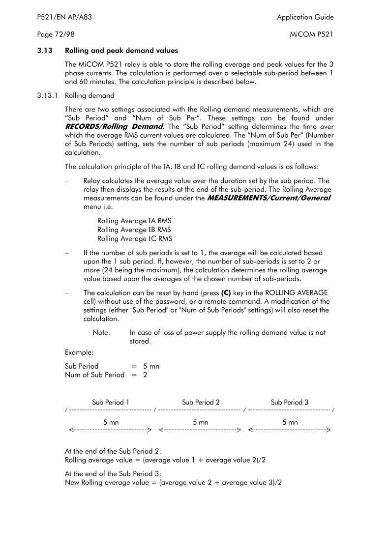
P521/EN AP/A83 Application Guide Page 72/98 MiCOM P521
3.13 Rolling and peak demand values
The MiCOM P521 relay is able to store the rolling average and peak values for the 3 phase currents. The calculation is performed over a selectable sub-period between 1 and 60 minutes. The calculation principle is described below.
3.13.1 Rolling demand
There are two settings associated with the Rolling demand measurements, which are “Sub Period” and “Num of Sub Per”. These settings can be found under RECORDS/Rolling Demand. The “Sub Period” setting determines the time over which the average RMS current values are calculated. The “Num of Sub Per” (Number of Sub Periods) setting, sets the number of sub periods (maximum 24) used in the calculation.
The calculation principle of the ΙA, ΙB and ΙC rolling demand values is as follows:
− Relay calculates the average value over the duration set by the sub period. The relay then displays the results at the end of the sub-period. The Rolling Average measurements can be found under the MEASUREMENTS/Current/General menu i.e.
Rolling Average ΙA RMS Rolling Average ΙB RMS Rolling Average ΙC RMS
− If the number of sub periods is set to 1, the average will be calculated based upon the 1 sub period. If, however, the number of sub-periods is set to 2 or more (24 being the maximum), the calculation determines the rolling average value based upon the averages of the chosen number of sub-periods.
− The calculation can be reset by hand (press (C) key in the ROLLING AVERAGE cell) without use of the password, or a remote command. A modification of the settings (either "Sub Period" or "Num of Sub Periods" settings) will also reset the calculation.
Note: In case of loss of power supply the rolling demand value is not stored.
Example:
Sub Period = 5 mn Num of Sub Period = 2
Sub Period 1 Sub Period 2 Sub Period 3
5 mn 5 mn 5 mn
At the end of the Sub Period 2: Rolling average value = (average value 1 + average value 2)/2
At the end of the Sub Period 3: New Rolling average value = (average value 2 + average value 3)/2
Application Guide P521/EN AP/A83 MiCOM P521 Page 73/98
3.13.2 Peak value demand
The Peak demand value calculation principle, for ΙA, ΙB and ΙC currents, is as follows:
Every "Rolling Sub Period", a new average value is calculated and compared with the value calculated during the previous "Rolling Sub Period". If this new value is greater than the previous value already stored, then the previous value is overwritten with the new one. However, if this new value is lower than the previous value, already stored, then the previous value is kept. In this way, an average peak value will be refreshed each Sub Period;
The Sub Period setting, used for the peak value calculation, is the same as that used for the rolling average calculation (RECORDS/Rolling Demand).
The 3 phase Peak value demand are displayed in the MEASUREMENTS/Current/General menu:
MAX SUBPERIOD ΙA RMS MAX SUBPERIOD ΙB RMS MAX SUBPERIOD ΙC RMS
− The calculation can be reset by hand (press (C) key in the MAX. SUBPERIOD cell) without use of the password, or a remote command. A modification of the "Sub Period" setting will also reset the calculation.
Note: In case of loss of power supply the Peak average values are stored in battery backed RAM.
3.14 Measurements
The MiCOM P521 relay has three different measurement columns, each one dedicated to specific relay functions. The three measurement columns are as follows:
− Current Diff
− Current/General
− Protection Comms
The following section describes the contents of the three measurement columns.
Note: All measurements listed below are updated on a per second basis.
3.14.1 Current diff
The measurements contained with the Current Diff column are associated with the current differential protection. These include remote phase currents and per phase differential and bias currents. Relays with firmware version 3 provide additional phase angle measurements: the phase angles between the currents in adjacent phases at the Local end, and the differential angles between each phase current at the Local end and the same phase current at the Remote end (time-aligned).
All measurements within this column are based upon the fundamental frequency only. All measurements contained within this column are multiplied by the local CT ratio setting, with the exception of the remote phase currents, which are scaled as follows:
Remote Current (primary) = Remote Secondary Current x Local CT Ratio
CT Correct Ratio
This calculation accounts for any CT mismatch between ends.

P521/EN AP/A83 Application Guide Page 74/98 MiCOM P521
3.14.2 Current/general
The relay produces a variety of directly measured and calculated power system quantities. The list of measurements include:
− Local Phase and Neutral RMS Currents
− Positive and negative sequence currents (Ι1 and Ι2 respectively)
− Ratio of Ι2/Ι1
− Residual harmonic currents
− Thermal state (%)
− Peak and average currents
− Demand values
The following section describes some of these measurements in more detail.
3.14.2.1 Measured currents
The RMS phase and earth currents are calculated by using the sum of the samples squared over a cycle of data.
3.14.2.2 Ratio of Ι2/Ι1
The ratio of Ι2/Ι1 is used to detect broken conductors. Refer to the broken conductor section for more information.
3.14.2.3 Residual harmonic currents (ΙN – fn)
This measurement allows the user to determine the harmonic currents (typically 3rd harmonic) flowing in the earth path. On pressing the (C) key, in the “ΙN – fn” cell, the relay will update the measurement of the actual RMS earth current minus the fundamental component. This measurement will only be updated on subsequent presses of the (C) key.
3.14.2.4 Peak and average currents
These measurements display the peak and average RMS currents over a settable time window of 5 to 60 minutes. The time window is set in the “Time Window” cell under the RECORDS/Time Peak Value menu. Once the time window has elapsed, the peak and average measurements will be stored until they are reset. To reset these measurements, and trigger another time window, the user must either press the (C) key, in the “Max & Average” cell, or modify the “Time Window” setting.
Note: The peak and average measurements will be lost in the event of an auxiliary supply interruption.
3.14.2.5 Demand values
See “Rolling and peak demand values” section.
3.14.3 Protection comms
This column allows the user to view various statistics relating to the protection communications channel.
A brief explanation of every measurement, contained in this column, can be found in section 3.5.3.3 of the User Guide (P521/EN FT).

Application Guide P521/EN AP/A83 MiCOM P521 Page 75/98
The protection comms statistics can be reset (with the exception of the propagation delay) by either pressing the (C) key, in the “Comms Stats RST cell” or by energizing an opto input, which has been assigned to “Comms RST”.
3.15 Logic Equations
The logic equations can be used to construct complex Boolean logic using the following operators: OR, OR NOT, AND, AND NOT.
An example logic implementation using Equation A is shown below:
&CB Fail
Input 1
1tAux1
0
0.5s
Ouptut
Figure 28 Example of logic equation
There are 8 equations of 16 operands chosen within all instantaneous and time-delayed events (thresholds and protections flags, tAux ...) and all inputs.
Every result of equation can be time delayed and assigned to any output relays, trip command, trip latching and/or HMI LEDs.
Every equation has a pick up time delay settable from 0 s to 600 s with a step of 0.01 s.
Every equation has a drop off time delay settable from 0 s to 600 s with a step of 0.01 s.
3.16 Current transformer supervision
Failure of current transformer circuit will result in mal-operation of any current depending protections, such as current differential, negative sequence, broken conductor and undercurrent. Now the P521 relay includes a current transformer supervision, which is called “Differential CTS”.
There are two modes of operation of CTS, Indication and Restrain. In Indication mode, a CTS alarm will be raised after the time delay expires but no effect on protection will occur. In Restrain mode, the Is1 setting of the Current Differential will be raised to the “CTS Is1” setting, which should normally be set to above load current. At same time, the local Broken Conductor, Under Current and Negative Sequence Overcurrent protections will be blocked.
The Differential CTS uses the following principle to detect a single phase or two phases CT failure: when a CT failure happens, the negative sequence current reflected into the relay will occur at only one side, while the primary currents at both sides keep normal.
The CTS function works on two current detectors:
I1 level detector – positive sequence current detector
The value of I1 shall be calculated compared with a user setting (I1>). The purpose of this element is to detect there is load current flowing in the line.

P521/EN AP/A83 Application Guide Page 76/98 MiCOM P521
The output of this element shall be transferred to the remote ends via the signaling message.
I2/I1 level detector – negative to positive ratio
The value of I2/I1 will be calculated and compared with two user settings (low set is I2/I1>, and high set is I2/I1>>). If the result is lower than I2/I1>, it means that the currents are balanced. When the result is higher than I2/I1>>, it means that a significant unbalanced current has occurred.
The output from each element will be transferred to the remote ends via the signaling message.
The purpose of these elements is to discriminate CT problems from asymmetrical faults including Broken Conductor fault.
Intsig: REM CTS I2/1>
Intsig:REM CTS I2/1>>
*
*
*
*
Intsig received in message
Intsig: REM CTS Enable ?
Intsig: REM CTS I1>&
&
&
*
0Pickupt
Auto ResetManual Reset 1
SR
QRemote CTS Alarm
0Pickupt
Auto ResetManual Reset 1
SR
Q Local CTS Alarm
Restrain Mode
0Pickup
20ms
&
1CTS Block&
CTS Block Diff
CTS Restrain Diff1
&Restrain Mode
Any Trip
CTS prohibited
&
XORCTS Config AlarmIntsig:LOC CTS Enable
Intsig:LOC CTS I1>
Intsig: LOC CTS I2/1>>
° Intsig Calculated Locally
°
°Intsig: LOC CTS I2/1>
°
°
&
&
Figure 29 Current transformer supervision
The logic diagram is shown in Figure 29. The “CTS Block” signal is used to inhibit the operating of broken conductor, negative sequence and undercurrent protections.
To use the CTS function, choose “Yes” under the menu AUTOMATIC. CTRL/CT Supervision/CTS ?. The settings are as below.
CT Supervision Default Setting
Min Max Step
CTS ? No Yes, No
CTS Reset mode Manual Manual, Auto

Application Guide P521/EN AP/A83 MiCOM P521 Page 77/98
CT Supervision Default Setting
Min Max Step
CTS Reset
RST=[C]
Press key (C) to reset CTS alarm. Visible only when CTS Reset mode is set in Manual.
CTS I1> 0.1 In 0.050 In 4 In 0.01 In
CTS I2/I1> 5% 5% 100% 5%
CTS I2/I1>> 40% 5% 100% 5%
CTS TIME DLY 5 s 0 s 10 s 0.01 s
CTS Restrain? No Yes, No
Note1: CTS function will work only when the relays are set in Extension communication mode in the menu COMMUNICATION/Protection/FRAME MODE.

P521/EN AP/A83 Application Guide Page 78/98 MiCOM P521
4. CURRENT TRANSFORMER REQUIREMENTS
4.1 Current differential protection
For accuracy, class X or class 5P current transformers (CTs) are strongly recommended, with a knee point voltage that complies with the requirements of the formula shown below. Simplified versions of the formula are shown in section 4.2, but these should only be used within the specified limits.
Vk ≥ Ks . Kt . In (Rct + 2RL)
Where:
Vk = Required IEC knee point voltage
Ks = Dimensioning factor
Kt = Operating time factor
In = CT nominal secondary current
Rct = CT dc resistance
RL = One-way lead impedance from CT to relay
4.1.1 Ks calculation
Ks is a constant depending upon:
If = Maximum value of through fault current for stability (multiple of In)
X/R = Primary system X/R ratio
Ks is determined as follows:
For X/R < 40
Ks = 0.023 x If (X/R + 55) + 0.9 (X/R+26)
For X/R ≥ 40
Ks = 0.024 x If (X/R + 44) + 0.06 (X/R+725)
4.1.2 Kt calculation
Kt is a constant depending upon:
X/R = Primary system X/R ratio
tIdiff = Current differential operating time setting (seconds)
For applications where the CT knee point is critical (e.g. a retrofit application where the CTs already exists), it may be possible to reduce the CT requirements by adding a small time delay to the relay. The ‘tIdiff’ (PROTECTION G1 (G2)/[87] Current Diff/tIdiff) setting allows the user to increase the relay operating time thus making the relay more stable. For some applications a time setting of 50ms may reduce the required CT knee point voltage by as much as 30%. Further reductions in CT knee point are possible with longer time delays.

Application Guide P521/EN AP/A83 MiCOM P521 Page 79/98
Kt is determined as follows:
For X/R < 40
Kt = 1 – (6.2 x tIdiff) for tIdiff ≤ 0.15s
Kt = 0.07 for tIdiff > 0.15s
For X/R ≥ 40
Kt = 1 – (2.5 x tIdiff) for tIdiff not exceeding 0.25s
For applications where the relay is set to instantaneous (tIdiff=0), a Kt value of 1 should be used.
4.2 Typical equations for current differential protection
The following equations can be applied for simplicity. Care must be taken to ensure that X/R and fault levels conform to the limits specified. If the calculated Vk appears to be too large, it may be necessary to ‘fine tune’ the calculation by using the equations specified in section 4.1.
For X/R ≤ 20 and a fault level ≤ 25 In
Vk ≥ 85 . Kt . In (Rct + 2RL)
For X/R < 40 and a fault level ≤ 25 In
Vk ≥ 99 . Kt . In (Rct + 2RL)
Where Kt is determined as follows:
Kt = 1 – (6.2 x tIdiff) for tIdiff ≤ 0.15 s
Kt = 0.07 for tIdiff > 0.15 s
Note: The equations shown in this section are based upon the equations in section 4.1 with the associated X/R and fault level figures already substituted.
4.3 Selection of X/R ratio and fault level
The value of X/R ratio and fault level will vary from one system to another, but selecting the correct value for the CT requirements is critical. In the case of single end fed (radial) systems the through fault level and X/R ratio should be calculated assuming the fault occurs at the location of the remote CT. For systems where the current can feed through the protected feeder in both directions, such as parallel feeders and ring main circuits, further consideration is required. In this case the fault level and X/R ratio should be calculated at both the local and remote CT’s. In doing this the X/R ratio and fault level will be evaluated for both fault directions. The CT requirements, however, should be based upon the fault direction that gives the highest knee point voltage. Under no circumstances should the X/R ratio from one fault direction and the fault level from the other be used to calculate the knee point. Doing this may result in exaggerated and unrealistic CT requirements.

P521/EN AP/A83 Application Guide Page 80/98 MiCOM P521
4.4 SEF protection – as fed by core-balance CT
Core balance current transformers of metering class accuracy are required and should have a limiting secondary voltage satisfying the formula given below:
Vk ≥ Ιfn x (Rct + 2RL + Rrn)
Where:
Vk = Required IEC knee point voltage
Ifn = Maximum prospective secondary earth fault current
Rct = CT dc resistance
RL = One-way lead impedance from CT to relay
Rrn = Impedance of neutral current input

Application Guide P521/EN AP/A83 MiCOM P521 Page 81/98
5. COMMUNICATION BETWEEN RELAYS
5.1 Communications link options
A number of communications options are available for the communication channel between P521 system ends. The various connection options are described below. Choosing between each of these options will depend on the type of communications equipment that is available.
Where existing suitable multiplexer communication equipment is installed, for other communication between substations, interfaces conforming to the G.703, V.35, and X.21 recommendations are available, by using the 850 nm fiber interface in the P521 plus a P591, P592 or P593 interface unit. For further information on the P591, P592 and P593 optical fiber to electrical interface units, refer to section 5.3.
Where no multiplexer is installed, the direct optical fiber connection can be used. The type of fiber used (multi-mode or single-mode) will be determined by the distance between the ends of the P521 relay system, refer to section 5.2.5.
For multiplexed or direct fiber communications the data rate may be selected as either 56 kbit/sec or 64 kbit/sec using the SDLC protocol. Slower data rates can be selected for these applications, but this is not recommended, as it would result in increased relay operating times.
Where a 2 wire unconditioned pilot wire circuit is available (i.e. pilot wires without any signal equalization equipment), baseband or mDSL modems can be used in conjunction with the P521 relays to communicate at 64 kbit/sec, refer also to section 5.5.
Where a 4 wire unconditioned pilot wire circuit is available a P595 can be used, refer also to section 5.4.
For 2 wire conditioned pilots (provided by a telecommunications company), a suitable type of modem must be used, and there is no strict limit to the distance. Refer to section 5.6.
For distances of 1.2 km or less and two twisted pairs of wires are available, EIA(RS)485 can be utilized at data rates of 64 kbit/sec, 56 kbit/sec, 19.2 kbit/sec and 9.6 kbit/sec, refer also to section 5.7.
In certain circumstances the user may want to change the relay protection communications interface. For example, from electrical (EIA(RS)485/232) to fiber optic, when the P521 is fitted in a substation with existing pilot/telephone wires, which are to be replaced with fiber optic cables at a later date. With a minor hardware change the relay can be upgraded without the need for a software/firmware change. Refer to section 9.4.4 of the Commissioning and Maintenance section of this manual (P521/EN CM) for information regarding communications interface changes.
5.2 Direct optical fiber
5.2.1 Direct optical fiber link, 850 nm multi-mode fiber
The relays are fitted with the 850 nm multi-mode fiber interface, and connected directly using two 850 nm multi-mode optical fibers for the signaling channel. Multi-mode fiber type 50/125µm or 62.5/125µm is suitable. BFOC/2.5 type fiber optic connectors are used. These are commonly known as “ST” connectors (“ST” is a registered trademark of AT&T).

P521/EN AP/A83 Application Guide Page 82/98 MiCOM P521
P521850nm MM
P521850nm MM
This is typically suitable for connection up to 1 km.
5.2.2 Direct optical fiber link, 1300 nm multi-mode fiber
The relays are fitted with the 1300 nm multi-mode fiber interface, and connected directly using two 1300 nm multi-mode fibers for the signaling channel. Multi-mode fiber type 50/125 µm or 62.5/125 µm is suitable. BFOC/2.5 type fiber optic connectors are used.
P5211300nm MM
P5211300nm MM
This is typically suitable for connection up to approximately 50 km (from December 2008). Pre-December 2008 relays were suitable for connection up to approximately 30 km.
5.2.3 Direct optical fiber link, 1300 nm single-mode fiber
The relays are fitted with the 130 nm single-mode fiber interface, and connected directly using two 1300 nm single-mode fibers, type 9/125 µm for the signaling channel. BFOC/2.5 type fiber optic connectors are used.
P5211300nm SM
P5211300nm SM
This is typically suitable for connection up to approximately 100 km (from December 2008). Pre-December 2008 relays were suitable for connection up to approximately 60 km.
5.2.4 Switched communication networks
The P521 relay makes use of digital communication signaling channels for the differential protection. For the P521 a requirement of this link is that ‘go’ (tp1) and ‘return’ (tp2) times are similar (a difference of up to 1 ms can be tolerated). Times greater than this can result in relay instability.
Where switched communications networks are used, it is possible that during switching, a transient time period may exist with different ‘go’ and ‘return’ times. The P521 relay includes a facility to ensure protection stability during this transient period.
One of the checks performed on the communications link is a check on the calculated propagation delay for each data message. During normal operation the difference in calculated time should be minimal (possible delays being introduced by multiplexers or other intermediary communication equipment). If successive calculated propagation delay times exceed a user settable value (200 – 10000 µs)

Application Guide P521/EN AP/A83 MiCOM P521 Page 83/98
then the data message is discarded. This check is used to overcome switching problems.
Figure 30 shows a possible scenario for a switched network. Initially the P521 relays are communicating via path 1. The go and return times for this path are 2 ms and hence the calculated propagation delay is (2 + 2)/2 = 2 ms. When the channel is switched to path 2, a small time period exists where the P521’s could be sending messages via path 1 and returning via path 2.
The calculated propagation delay will now be (2 + 5)/2 = 3.5 ms. The resultant 1.5 ms error at each line end may cause the relay to maloperate due to incorrect time alignment of current vectors (see section 2.1.2). After a short delay, both ‘go’ and ‘return’ paths will follow route 2 and the calculated propagation delay will be (5 + 5)/2 = 5 ms. The relay will now be stable, as correct current vector time alignment exists at each line end.
The P521 relay uses the change in calculated propagation delay to initiate a change in relay characteristic for a short time period (COMMUNICATION/Protection/ Char Mod Time setting) to overcome any switching delay. The Char Mod timer is settable in the range 0 to 100 seconds, default 10 seconds. The change in characteristic is shown in Figure 26 whereby the relay Ιs1 setting is increased to 200% of Ιs2 and the k1 slope is changed to 0%. This characteristic provides stability for all load conditions and will still allow tripping for most internal fault conditions.
The Char Mod timer is started when a change in propagation delay is detected. Any subsequent change during this period will not cause the timer to restart. In the above example the timer will start for the first change (2 to 3.5 ms). The second change (3.5 ms to 5 ms) will not cause the timer to restart, which would prolong the setting change.
Any transient “jitter” occurring on the communications path, which affected the propagation delay time, could therefore unnecessarily desensitize the relay. To overcome this possible problem, the P521 relay includes a feature whereby the Char Mod timer is reset if a change is detected during its timing period that returns the propagation delay to its original value. The dotted line of Figure 30 shows this, where the propagation delay changes from 2 to 3.5 ms and back to 2 ms.

P521/EN AP/A83 Application Guide Page 84/98 MiCOM P521
! (" !!
"
C("!-%*.$!("'
("
* # !!
(
"
3"
"
*!""#&!
E#"
*!""#&!
E#" .
F!F"
F#F"
.
F!F"
F#F"
Figure 30 Switched communication network
Figure 31 Modified bias characteristic

Application Guide P521/EN AP/A83 MiCOM P521 Page 85/98
5.2.5 Optical budgets
When applying the P521 current differential relay, it is important to select the appropriate fiber interface. This will depend on the fiber used and distance between devices. The following table shows the optical budgets of the available communications interfaces.
From December 2008 850 nm Multi-Mode
1300 nm Multi-Mode
1300 nm Single-Mode
Min. transmit output level (average power)
-19.8 dBm -6 dBm -6 dBm
Receiver sensitivity (average power)
-25.4 dBm -49 dBm -49 dBm
Optical budget 5.6 dB 43.0 dB 43.0 dB
Less safety margin (3 dB) 2.6 dB 40.0 dB 40.0 dB
Typical cable loss 2.6 dB/km 0.8 dB/km 0.4 dB/km
Max. transmission distance 1 km 50.0 km 100.0 km
Table 22: Optical budgets
Note: From December 2008, the optical budgets and hence also the maximum transmission distances of the 1300 nm multi-mode and 1300 nm single-mode fiber interfaces have been increased, to the values shown in the table above.
The new interface cards are identified by “43dB” marked in the centre of the backplate, visible from the rear of the relay. These new fiber interfaces are fully backward-compatible with the original equivalent interface. However, in order to achieve the increased distance, both ends of the P521 scheme would need to use the new interface.
Pre-December 2008 relays will have the original optical budgets and maximum transmission distances, as shown below.
Pre-December 2008 850 nm Multi Mode
1300 nm Multi Mode
1300 nm Single Mode
Min. transmit output level (average power) -19.8 dBm -10 dBm -10 dBm
Receiver sensitivity (average power) -25.4 dBm -37 dBm -37 dBm
Optical budget 5.6 dB 27.0 dB 27.0 dB
Less safety margin (3dB) 2.6 dB 24.0 dB 24.0 dB
Typical cable loss 2.6 dB/km 0.8 dB/km 0.4 dB/km
Max. transmission distance 1 km 30.0 km 60.0 km
Table 23: Optical budgets

P521/EN AP/A83 Application Guide Page 86/98 MiCOM P521
The total optical budget is given by the transmitter output level minus the receiver sensitivity and will indicate the total allowable losses that can be tolerated between devices. A safety margin of 3 dB is also included in the above table. This allows for degradation of the fiber as a result of ageing and any losses in cable joints. The remainder of the losses will come from the fiber itself. The figures given are typical only and should only be used as a guide.
In general, the 1300 nm interfaces will be used for direct connections between relays. The 850 nm would be used where multiplexing equipment is employed.
5.3 Multiplexer link via P59x optical fiber to electrical interface units
In order to connect the P521 relay via a pulse code modulation (PCM) multiplexer network or digital communication channel the P59x interface units are required. The following interface units are available:
− P591 interface to multiplexing equipment supporting ITU-T (formerly CCITT) Recommendation G.703 co-directional electrical interface
− P592 interface to multiplexing equipment supporting ITU-T Recommendation V.35 electrical interface
− P593 interface to multiplexing or ISDN equipment supporting ITU-T Recommendation X.21 electrical interface
The data rate for each unit can be 56kbit/sec or 64kbit/sec as required for the data communications link, refer to section 5.11.
One P59x unit is required per relay signaling channel (i.e. for each transmit and receive signal pair). It provides optical to electrical and electrical to optical signal conversion between the P521 relay and the multiplexer. The interface unit should be located as close to the PCM multiplexer as possible, to minimize any effects on the data of electromagnetic noise or interference.
The units are housed in a 20 TE MiCOM case.
Fiber optic connections to the unit are made through BFOC/2.5 type connectors, more commonly known as ‘ST’ connectors.
The optical characteristics are similar to the P521 850 nm multi-mode fiber optic interface (refer to section 5.2.5 above).
5.3.1 Multiplexer link with G.703 electrical interface using auxiliary optical fibers and type P591 interface
The relays are fitted with the 850 nm optical interface, and connected to a P591 unit by 850 nm multi-mode optical fiber. Multi-mode fiber type 50/125 µm or 62.5/125 µm is suitable. BFOC/2.5 type fiber optic connectors are used. The P591 unit converts the data between optical fiber and ITU-T compatible G.703 co-directional electrical interface. The G.703 output must be connected to an ITU-T compatible G.703 co-directional channel on the multiplexer.
!:&"&"
!:1;
1;
<=9 <=9
4:
!4!
!4!
The P591 unit supports the ITU-T Recommendation G.703 co-directional interface.

Application Guide P521/EN AP/A83 MiCOM P521 Page 87/98
The P591 interface unit should be located as close to the PCM multiplexer as possible, to minimize any effects on the data of electromagnetic noise or interference.
The G.703 signals are isolated by pulse transformers to 1kV.
Since the G.703 signals are only of ±1V magnitude, the cable connecting the P591 unit and the multiplexer must be properly screened against electromagnetic noise and interference. The interface cable should consist of twisted pairs of 24 AWG, overall shielded, and have a characteristic impedance of about 120 Ω. It is generally recommended that the interface cable shield should be connected to the multiplexer frame ground only. The choice of grounding depends upon the local codes of practice.
Electrical connections to the P591 unit are made via a standard 28-way Midos connector. Please refer to P521/EN CO for the external connection diagram.
The P521 must be set with Clock Source as ‘External’, refer to section 5.10.
5.3.2 Multiplexer link with V.35 electrical interface using auxiliary optical fibers and type P592 interface
The relays are fitted with the 850 nm optical interface, and connected to a P592 unit by 850 nm multi-mode optical fiber. Multi-mode fiber type 50/125 µm or 62.5/125 µm is suitable. BFOC/2.5 type fiber optic connectors are used. The P592 unit converts the data between optical fiber and ITU-T compatible V.35 electrical interface. The V.35 output must be connected to an ITU-T compatible V.35 channel on the multiplexer.
4:
!:4&"&"
!:41;
1;
>9! >9!!4!
!4!
The P592 unit supports the ITU-T Recommendation V.35 interface.
The P592 interface unit should be located as close to the PCM multiplexer as possible, to minimize any effects on the data of electromagnetic noise or interference.

P521/EN AP/A83 Application Guide Page 88/98 MiCOM P521
Connections of V.35 signals to the P592 unit are made via a standard female 34 pin ‘M’ block connector. Since the V.35 signals are either of ±0.55 V or ±12 V magnitude, the cable connecting the unit to the multiplexer must be properly screened against electromagnetic noise and interference. The interface cable should consist of twisted pairs of wires which are shielded, and have a characteristic impedance of about 100 Ω. It is generally recommended that the interface cable shield is connected to the multiplexer frame ground. The choice of grounding depends upon the local codes of practice.
The P592 front panel consists of five indicating LEDs and six DIL (dual in line) switches.
The switch labeled ‘Clockswitch’ is provided to invert the V.35 transmit timing clock signal if required.
The switch labeled ‘Fiber-optic Loopback’ is provided to allow a test loopback of the communication signal across the fiber optic terminals. When switched on, the red LED labeled 'Fiber-optic Loopback' is illuminated.
The switch labeled ‘V.35 Loopback’ is provided to allow a test loopback of the communication signal across the X.21 terminals. It loops the incoming V.35 ‘Rx’ data lines internally back to the outgoing V.35 ‘Tx’ data lines. When switched on, the red LED labeled ‘V.35 Loopback’ is illuminated.
The switch labeled ‘DSR’ is provided to select/ignore the DSR (Data Set Ready) handshaking control signal. The red LED labeled DSR Off is extinguished either when DSR is asserted or when overridden by setting the DSR switch On.
The switch labeled ‘CTS’ is provided to select/ignore the CTS (Clear To Send) handshaking control signal. The red LED labeled CTS Off is extinguished either when CTS is asserted or when overridden by setting the CTS switch On.
The switch labeled ‘Data Rate’ is provided to allow the selection of 56 or 64 kbit/sec data rate, as required by the PCM multiplexing equipment.
The green LED labeled ‘Supply Healthy’ provides indication that the unit is correctly powered.
Please refer to P521/EN CO for the external connection diagram.
The P521 may be set either with Clock Source as ‘External’ for a multiplexer network which is supplying a master clock signal, or with Clock Source as ‘Internal’ for a multiplexer network deriving its signal timing from the equipment. Refer to section 5.10.
5.3.3 Multiplexer link with X.21 electrical interface using auxiliary optical fibers and type P593 interface
The P593 unit supports the ITU-T Recommendation X.21 interface. It is approved as line interface equipment by the British Approvals Board for Telecommunications (BABT) for connection to the services described in this section; License Certificate Number NS/1423/1/T/605362.

Application Guide P521/EN AP/A83 MiCOM P521 Page 89/98
The relays are fitted with the 850 nm optical interface, and connected to a P593 unit by 850 nm multi-mode optical fiber. Multi-mode fiber type 50/125 µm or 62.5/125 µm is suitable. BFOC/2.5 type fiber optic connectors are used. The P593 unit converts the data between optical fiber and ITU-T compatible X.21 electrical interface. The X.21 output must be connected to an ITU-T compatible X.21 channel on the multiplexer or ISDN digital data transmission link.
=
= >#
?$@A
,
,
>#?$
=@A
The P593 interface unit should be located as close to the PCM multiplexer as possible, to minimize any effects on the data of electromagnetic noise or interference.
The P521 relays require a permanently open communications channel. Consequently, no communications handshaking is required, and it is not supported in the P593 unit. The signals supported are shown in table 23.
ITU-T Recommendation X.21 is closely associated with specifications EIA(RS)422 and EIA(RS)449. The P593 can be used with EIA(RS)422 or EIA(RS)449 communications channels which require only the signals shown overleaf.
ITU-T Designation
Description Connector
Pin Direction
- Case earth 1 -
G Common return 8 -
T Transmit data A 2 From P593
T Transmit data B 9 From P593
R Receive data A 4 To P593
R Receive data B 11 To P593
S Signal element timing A 6 To P593
S Signal element timing B 13 To P593
Table 24: X.21 circuits supported by P593 unit
Connections of X.21 signals to the P593 unit are made via a standard male 15 way D-type connector, wired as a DTE device. The interface cable should consist of twisted pairs of 24 AWG, overall shielded, and have a characteristic impedance of about 100 Ω. It is generally recommended that the interface cable shield is connected to the multiplexer frame ground. The choice of grounding depends upon the local codes of practice.
Refer to P521/EN CO for the external connection diagram.
The P521 must be set with Clock Source as ‘External’, refer to section 5.10.
The P593 front panel consists of four indicating LEDs and two switches.
The green LED labeled ‘Supply healthy’ provides indication that the unit is correctly powered.
The green LED labeled ‘Clock’ provides indication that an appropriate X.21 signal element timing signal is presented to the unit.

P521/EN AP/A83 Application Guide Page 90/98 MiCOM P521
One of the switches is labeled ‘Fiber Optic Loopback’. This is provided to allow a test loopback of the communication signal across the fiber optic terminals. When switched on, the red LED labeled ‘Fiber Optic Loopback’ is illuminated.
The second switch is labeled ‘X.21 Loopback’. This is provided to allow a test loopback of the communication signal across the X.21 terminals. It loops the incoming X.21 ‘Rx’ data lines internally back to the outgoing X.21 ‘Tx’ data lines, and also loops the incoming fiber optic ‘Rx’ data line (via the X.21 signal conversion circuitry) back to the outgoing fiber optic ‘Tx’ data line. When switched on, the red LED labeled ‘X.21 Loopback’ is illuminated.
5.4 Unconditioned 4 wire pilot communications for distances greater than 1.2 km (P595)
In order to increase the transmission distance of EIA(RS)485 up to 25 kilometres the P595 Interfacing Device can be used at each end of the line. To gain maximum performance of the P521, the data rate must be set to 19.2 kbit/sec and the protocol set to “NRZ” (Non Return to Zero).
The relays are fitted with the EIA(RS)485 interface, and connected using two pairs of unconditioned pilot wires of 0.4 mm (26 AWG) or larger gauge, twisted and shielded to ensure secure and reliable communications.
Pilot isolation must also be considered, when connecting the P595. If the longitudinal voltage exceeds 900 V the PCM-FLÜ 10 kV or 20 kV isolating transformers must be fitted in series with the P595. The PCM-FLÜ isolating transformer has “a”, “m” and “b” taps on both primary and secondary windings. For all P521 applications, connection must be made between taps ‘a’ and ‘m’, which has a maximum frequency of 2 MHz. Connection between ‘a’ and ‘b’ may result in unreliable communications as the maximum frequency for this tap configuration is 6 kHz. Connection to ‘a’ and ‘m’ taps must be adhered to on both primary and secondary so as to maintain a 1:1 ratio.
Refer to section P521/EN CO for connection diagrams.
Refer to the P595 manual (P595/EN M) for further information.
Note: The P595 interface device is identical to the Schneider Electric T&D PZ511 interface except that the P595 has accessible setting switches. The switch settings, to allow communications between P521 relays, can be found in the P595 manual.

Application Guide P521/EN AP/A83 MiCOM P521 Page 91/98
5.5 Unconditioned 2 wire pilot communications for distances greater than 1.2 km
When communicating via a pair of unconditioned pilots for distances greater than 1.2 km, a leased line or baseband modem can be used. For maximum security and performance it is strongly recommended that a screened twisted pair of 0.5 mm (or greater) conductors are used. Typical connection diagrams are shown in section P521/EN CO.
When choosing between leased line or baseband modems the following aspects should be considered:
− Leased line modems have a maximum transmission speed of 19.2 kbit/sec, whereas baseband modems can transmit at 64 kbit/sec.
− Baseband modems have longer re-training times, typically between 10 to 60 s. If the connection between is temporarily lost, the protection communications will be interrupted until the re-training period has elapsed.
− Since baseband modems use synchronous communication protocols, there is typically a 20% performance gain over leased line modems that use asynchronous protocols.
Modems tested:
− Westermo TD-32 leased line and dial-up modem. This model is obsolete and its replacement is:
− TD-36 modem
− Patton “Netlink” 1095 mDSL Baseband modem.
− Patton “Campus” 1092A Baseband Modem. This model is obsolete and its replacement is:
− Keymile LineRunner DTM modem with V36 interface.
Modem summary table. For full information see the modem configuration document P521/EN MC.
Type Max Distance
(km)
Recommended Data Rate (kbit/sec)
Typical Re-train Time (Seconds)
TD32 (Obsolete) 20 9.6 14
TD36 20 19.2 5
“Netlink”1095 9.4 64 25
“Campus” 1092A (Obsolete)
17.2 64 10
LineRunner DTM 19.8 64 -
The “Campus” 1092A modem may also be used for 4 wire pilot communications, giving extra security and a slightly improved maximum distance (18.2 km).
P521/EN AP/A83 Application Guide Page 92/98 MiCOM P521
5.5.1 Leased line modem set up (e.g. TD36 modem)
The data rate can be set to either 9.6 or 19.2 kbit/sec and the protocol set to “NRZ” (Non Return to Zero). Since the transmission speed is limited to 19.2 kbit/sec, connections to the modem can be made via EIA(RS)232 or EIA(RS)485 depending upon the type of modem.
Refer to P521/EN MC (modem configuration) for more information on setting up the modem.
5.5.2 Baseband modem set up (Patton “Netlink” 1095 mDSL modem, Patton “Campus” 1092A modem)
The data rate must be set to 64 kbit/sec, the protocol set to “NRZ”. For more information, on setting up the modem, refer to P521/EN MC (modem configuration).
5.5.3 Modem isolation
Pilot isolation must be considered when connecting modems to unconditioned circuits. Additional isolation can be provided by the PCM-FLÜ 10 kV or 20 kV isolating transformers. The PCM-FLÜ isolating transformer has “a”, “m” and “b” taps on both primary and secondary windings. For all P521 applications, connection must be made between taps ‘a’ and ‘m’, which has a maximum frequency of 2 MHz. Connection between ‘a’ and ‘b’ may result in unreliable communications as the maximum frequency for this tap configuration is 6 kHz. Connection to ‘a’ and ‘m’ taps must be adhered to on both primary and secondary so as to maintain a 1:1 ratio.
Refer to P521/EN AC for more information.
5.5.4 Clock source settings
Set relay Clock Source setting (COMMUNICATION/Protection/Clock Source CH1).
Modem Type Clock Source Setting
Synchronous External
Asynchronous Internal
5.6 Conditioned pilot communications
When communicating via conditioned pilot wires (i.e. leased telecom circuits that run through signal equalization equipment) the P521 should be connected to leased line modems at each end of the line. The data rate can be set to either 9.6 or 19.2 kbit/sec. The protocol must be set to “NRZ” (Non Return to Zero).
Modem summary table: For full information see the modem configuration document P521/EN MC.
Type Max Distance
(km)
Recommended Data Rate (kbit/sec)
Typical Re-train Time (Seconds)
TD36 n/a 9.6 5
Connection to the modem can be made via the EIA(RS)485 or EIA(RS)232 outputs (of SK1), depending upon the type of modem. Typical connection diagrams are shown in section P521/EN CO. For more information on setting up the modem refer to P521/EN MC (modem configuration).

Application Guide P521/EN AP/A83 MiCOM P521 Page 93/98
5.6.1 Gas discharge tubes (GDT’s)
Gas discharge tubes are commonly used to provide overvoltage/surge protection for conditioned pilots circuits. These are dispersed at intervals along the pilot circuit to limit the voltage between pilots and ground during heavy earth faults. The GDT’s limit the high potential by transiently shorting the pilots to both each other and ground. This, however, will temporarily interrupt the protection communications, thus preventing the protection from operating when required to do so. To prevent interruptions in the protection communications it is recommended that either:
• The earth fault level is checked to ensure that the resulting pilot voltage is less than the voltage threshold of the GDT’s (use equations from section 5.8)
or
• The GDT’s be removed and replaced with pilot isolation transformers
5.7 Direct 4 wire EIA(RS)485 up to 1.2 km
Direct connection between two P521 relays using 4 wire EIA(RS)485 can be used at data rates of 9.6, 19.2, 56 and 64 kbit/sec. The protocol for this communication method can be either “SDLC” or “NRZ”. Ideally the interconnecting wires should be 2 screened twisted pairs.
For the direct EIA(RS)485 connections up to 1.2 km it is strongly recommended that the MT-RS485 be fitted. The MT-RS485 protects the relay communications interface from excessive transverse voltages (voltage between pilot cores) and static spikes. However, for reliable communications it must be ensured that the longitudinal voltage never exceeds 600 V as the MT-RS485 surge protection may corrupt the protection signaling. Figure 29 shows the connection diagram for the MT-RS485.
5
4
G
5
4
G
(1
(1&
1
1&
& #
+!-" *"
%
H0/I.#!!
Figure 32 MT-RS485 connection diagram
Refer to section P521/EN CO for application diagram.
P521/EN AP/A83 Application Guide Page 94/98 MiCOM P521
5.8 Pilot isolation
During primary earth faults the strong magnetic field generated can induce a significant voltage between the pilots and ground (longitudinal voltage). To prevent damage to any equipment connected to the pilot circuit it must be ensured that the modem can provide an adequate isolation barrier between the pilot itself and all other electrically isolated circuits. Although it may be difficult to accurately predict the induced pilot voltage during an earth fault, the following equations can be used to give an approximation:
Induced voltage for un-screened pilots ≈ 0.3 x ΙF x L
Induced voltage for screened pilots ≈ 0.1 x ΙF x L
Where:
ΙF = Maximum prospective earth fault current in amperes
L = Length of pilot circuit in miles
In cases where the calculated voltage exceeds, typically 60% of the relay/modem isolation level, additional isolation must be added. Schneider Electric T&D offer the PCM-FLÜ 10kV or 20kV isolating transformers (see P521/EN AC for more information). If necessary, these can be used in conjunction with leased line or mDSL modems. The choice of 10 kV or 20 kV will depend upon the magnitude of the induced voltage. Typical application diagrams of the PCM-FLÜ isolating transformer are shown in section P521/EN CO (connection diagrams).
5.9 Protection communications address
The protection communication messages include an address field to ensure correct scheme connection.
There are 32 addresses arranged into 16 groups (COMMUNICATION/ Protection/Relay Address) to select from. Each protection system has a single group applied to it.
All the address patterns are carefully chosen so as to provide optimum noise immunity against bit corruption. There is no preference as to which address group is better than another.
The groups of addresses available for a “2 Terminal” scheme are as follows:
Relay A Relay B
Address Group 1 1A 1B
Address Group 2 2A 2B
Address Group 3 3A 3B
Address Group 4 4A 4B
Address Group 5 5A 5B
Address Group 6 6A 6B
Address Group 7 7A 7B
Address Group 8 8A 8B
Address Group 9 9A 9B
Address Group 10 10A 10B
Application Guide P521/EN AP/A83 MiCOM P521 Page 95/98
Relay A Relay B
Address Group 11 11A 11B
Address Group 12 12A 12B
Address Group 13 13A 13B
Address Group 14 14A 14B
Address Group 15 15A 15B
Address Group 16 16A 16B
Table 24: Relay addresses
For two relays to communicate with one another their addresses have to be in the same address group. One relay should be assigned with address A and the other with address B. For example, if the group 1 addresses are to be used, the one relay should be set to address “1A” and the other relay should be set to address “1B”.
A relay with address “1A” will only accept messages from a relay with address “1B”, and vice versa.
5.10 Clock Source
A clock Source is required to synchronize data transmissions between the system ends. This may be provided either by the P521 relay (internal) or may be a function of the telecommunications equipment (external). The P521 relay has a setting that allows the Clock Source to either “Internal” or “External” according to the communications system configuration (COMMUNICATION/Protection/Clock Source Ch1).
5.10.1 Internal Clock Source signaling
The Clock Source should be set to “Internal” at all system ends, where they are connected by direct optical fiber as the P521 at each end has to supply the clock.
5.10.2 External Clock Source
The Clock Source should be set to “External” at all system ends, where the ends are connected by multiplexer equipment which is receiving a master clock signal from the multiplexer network. It is important that there is a single master Clock Source on the multiplexer network and that the multiplexer equipment at each end is synchronized to this clock.
5.11 Data Rate
The Data Rate for signaling between the two ends is application specific (COMMUNICATION/Protection/Data Rate).
If there is a direct fiber connection between the ends, the data rate would usually be set to 64kbit/sec, as this gives a slightly faster trip time.
If there is a multiplexer network between the ends, then this will determine the Data Rate to be used by the P521 system. The electrical interface to the multiplexer (G.703 co-directional, V.35, or X.21) will be provided on either a 64 kbit/sec or 56 kbit/sec channel, and the P521 at each end must be set to match this data rate.
Generally, North American multiplexer networks are based on 56 kbit/sec (and multiples thereof) channels, whereas multiplexer networks in the rest of the world are normally based on 64 kbit/sec (and multiples thereof) channels.

P521/EN AP/A83 Application Guide Page 96/98 MiCOM P521
Refer to sections 5.4 to 5.7 for typical data rates for metallic/modem communications.
5.12 Communication failure
An internal communication failure flag is raised if a valid message is not received by the time three power system cycles have elapsed. The flag is used to trigger the communications fail timer. The flag and timer reset when the first valid message is received.
5.12.1 ‘I DIFF FAIL’ alarm
The ‘Ι DIFF FAIL’ alarm is generated when the communication failure flag is raised (if a valid message is not received by the time three power system cycles have elapsed). At this time, the current differential protection is inhibited.
If the CONFIGURATION/Alarms/Inst.Self-reset? menu cell is set to “Yes”, then the ‘Ι DIFF FAIL’ alarm automatically resets when the internal communication flag is reset; otherwise the alarm reset must be done by the push button.
5.12.2 ‘COMMS ALARM CH1’ alarm
The communication fail timer (COMMUNICATION/Protection/Comm Fail Timer) is the time for which communication errors must be continuously detected before the channel is declared failed. Expiry of the communication fail timer results in the generation of the ‘COMMS ALARM CH1’ alarm. The COMMUNICATION/Protection/Comm Fail Timer setting is normally set to the maximum of 9.9 seconds so that the alarm will not be given for short bursts of noise or interruptions.
If the CONFIGURATION/Alarms/Comm.Fail-reset? menu cell is set to “Yes”, then the ‘COMMS ALARM CH1’ alarm automatically resets when the internal communication flag is reset; otherwise the alarm reset must be done by the push button.
5.12.3 Communications failure logic
Figure 33 details the operation of the communications fail logic.
44$
:
##
$79
)12/% 4
1%)12
&&"-'!'B
%&%./ -//3%&%./C
+, -//3
&0 -//3
$$
12 $$ "
.&%* )12
&0 )12
%&%./
&0
0 % &
0 % &
Figure 33 Communications failure logic
Application Guide P521/EN AP/A83 MiCOM P521 Page 97/98
5.13 Communication error statistics
To aid the bit error evaluation of the communication link, communication error statistics are kept by the relay. These give the number of Errored messages detected and the number of Valid Messages received for the communications channel. The number of errored messages detected complies with ITU-T G.821.
The stored error statistics are:
Valid messages - Number of messages received OK
Errored messages - Number of messages received and rejected
Errored seconds - Number of seconds containing 1 or more errored messages. This is not updated for severely errored seconds
Severely errored seconds - Number of seconds containing ≥30% errored messages
Propagation delay - The delay introduced by the communications channel
Elapsed time since reset - The number of seconds since the communications error statistics were last reset
The error statistics are automatically restored on power-up. They can also be cleared using the Clear Statistics setting in Measurements column of the menu.
5.14 Communications delay tolerance timer
The communications delay tolerance timer (COMMUNICATION/Protection/ Comms Delay Tol) is the maximum difference in the measured channel propagation delay time between consecutive messages that the relay will tolerate before switching the settings, as described in section 5.2.4.
It is settable in the range 200 µs to 10 ms. The default value is 10 ms, which is suitable for protection communications using metallic/modem communications at lower data rates. A setting of 200 µs is more appropriate for a data rate of 56 or 64 kbit/sec. It can be increased to a suitable value if the propagation delay time is expected to vary considerably such as in the case of a microwave link with multiple repeaters.
5.15 Communication compatibility
The compatibilities among various software versions are (also refer to the chapter P521_EN_VC):
− Among phase 1: all V1 up to V5.A
− Between phase 1 and phase 2: V5.B and later to V10.A and later
− Among all phase 2: V10.A and later

P521/EN AP/A83 Application Guide Page 98/98 MiCOM P521
Communication P521/EN GC/A83 MiCOM P521
MODBUS AND DNP3.0 DATABASE IEC 60870-5-103
MiCOM P521
Date: 1st October 2010
Software version: 12
Connection diagram: 10P52101

P521/EN GC/A83 Communication MiCOM P521

Communication P521/EN GC/A83 MiCOM P521 Page 1/90
CONTENTS
1. INTRODUCTION 5
1.1 Purpose of this document 5
2. MODBUS PROTOCOL 5
2.1 Technical characteristics of the MODBUS connection 5
2.1.1 MODBUS setting parameters 5
2.1.2 Message synchronization 6
2.1.3 Message validity check 6
2.1.4 MiCOM relay addressing 6
2.2 MODBUS functions of the MiCOM relays 6
2.3 MODBUS function operation 6
2.3.1 Introduction 6
2.3.2 Request by the master 6
2.3.2.1 Slave address 6
2.3.2.2 Function codes 7
2.3.2.3 Structure of the information field by MODBUS function 7
2.3.2.4 CRC16 7
2.3.3 Format of the P521 response to a request from a master 7
2.3.3.1 Slave number 7
2.3.3.2 Function code 7
2.3.3.3 Structure of the data field by MODBUS function 7
2.3.3.4 Byte and word order 8
2.3.3.5 CRC16 8
2.3.4 Messages validity check 8
2.3.4.1 Exception response 8
2.3.4.2 Slave number 9
2.3.4.3 Function code 9
2.3.4.4 Exception code 9
2.3.4.5 CRC16 9
2.3.5 Slave access control 9
3. MODBUS IMPLEMENTATION 9
3.1 Overview 9
3.2 3 Dimensional MODBUS registers 10

P521/EN GC/A83 Communication Page 2/104 MiCOM P521
3.3 Mapping 10
3.3.1 Page 0H: product information 10
3.3.2 Page 1: non protection settings 15
3.3.3 Page 2h: group 1 protection settings 23
3.3.4 Page 4h: remote control words 27
3.3.5 Pages 5h: Boolean Equation 27
3.3.6 Page 6h: Boolean equation timers, programmable inter-trip and CTS 34
3.3.7 Page 7h: quick read relay status (MODBUS 07 function) 36
3.3.8 Page 8h: time synchronization 36
3.3.8.1 Private format 36
3.3.8.2 IEC time and date format 36
3.3.9 Diagnostics and communications event counters 37
3.3.9.1 Diagnostics counters (MODBUS Function 8) 37
3.3.9.2 Communications event counter (MODBUS Function 11) 38
3.4 Register format 39
3.5 Event record 60
3.5.1 Specific event record extraction 60
3.5.1.1 Page 35h: contains 75 event records from 3500h to 354Ah 60
3.5.1.2 Event record format 61
3.5.1.3 Event table 61
3.5.2 Page 36h: oldest event record 65
3.5.3 Event acknowledgement 66
3.5.3.1 Event acknowledgement mode 66
3.5.3.2 Automatic event acknowledgement mode 66
3.5.3.3 Manual event acknowledgement 66
3.5.3.4 Event acknowledgement control 66
3.6 Fault record 66
3.6.1 Specific fault record 66
3.6.1.1 Page 37h: fault record mapping 66
3.6.1.2 Fault record format 67
3.6.1.3 Fault record calculation formulae 69
3.6.1.4 Internal CT value for each sensitivity range 69
3.6.2 Oldest non acknowledged fault record 70
3.6.2.1 Page 3Eh: oldest non acknowledged fault record 70
3.6.3 Fault record acknowledgement 70
3.6.4 Event acknowledgement 70

Communication P521/EN GC/A83 MiCOM P521 Page 3/90
3.6.4.1 Event acknowledgement mode 70
3.6.4.2 Automatic event acknowledgement mode 70
3.6.4.3 Manual event acknowledgement 70
3.7 Disturbance records 70
3.7.1 Summary disturbance records 71
3.7.1.1 Page 3Dh: summary disturbance records 71
3.7.1.2 Format of summary disturbance records 71
3.7.2 Channel selection and configuration 72
3.7.2.1 Pages 38h to 3Ch: data mapping 72
3.7.2.2 Disturbance record channel selection and configuration format 73
3.7.3 Channel data 74
3.7.3.1 Page 9h to 21h: channel data mapping 74
3.7.3.2 Format of the disturbance record channel data 74
3.7.3.3 Calculation formulae 75
3.7.4 Disturbance recorder index frame 76
3.7.4.1 Page 22h: index frame mapping 76
3.7.4.2 Index frame format 76
3.8 Commonly required functionality 76
3.8.1 CB trip and close 76
3.8.2 Bit address 76
3.8.3 Bit value 76
3.8.4 Change setting group 77
3.8.4.1 Change setting group request 77
4. IEC 60870-5-103 PROTOCOL 77
4.1 Technical characteristics of the IEC 60870-5-103 connection 77
4.2 IEC 60870-5-103 compatible application functions 77
4.3 Application functions 78
4.3.1 Initialization (reset) 78
4.3.2 Time synchronization 78
4.3.3 Event record extraction 78
4.3.4 General interrogation 79
4.3.5 Cyclic measurements 79
4.3.6 General commands 79
4.3.7 Disturbance record extraction 79
4.3.7.1 Extracting disturbance records via the MODBUS front port 79
P521/EN GC/A83 Communication Page 4/104 MiCOM P521
4.3.8 Blocking of monitor direction 80
4.3.9 Test mode 80
5. IEC 60870-5-103 DETAILED IMPLEMENTATION 81
5.1 Compatible range information numbers in monitor direction 81
5.2 Compatible range information numbers in control direction 83
5.3 Private range information numbers in monitor direction 83
5.4 Private range information numbers in control direction 84
6. DNP3.0 INTRODUCTION 85
6.1 Purpose of this document 85
6.2 DNP V3.00 device profile 85
6.3 Implementation Table 88
6.4 Point list 92
6.4.1 Binary input points 92
6.4.2 Binary output status points and control relay output block 98
6.4.3 Counters 99
6.4.4 Analog Inputs 100

Communication P521/EN GC/A83 MiCOM P521 Page 5/90
1. INTRODUCTION
1.1 Purpose of this document
This chapter describes the data model of the different communication protocols of the P521 relay.
The available communication protocols of the MiCOM P521 relay are as follows:
− MODBUS RTU
− IEC 60870-5-103
− DNP3.0
2. MODBUS PROTOCOL
MiCOM P521 relays can communicate by an EIA(RS)485 link behind the unit following the MODBUS RTU protocol.
2.1 Technical characteristics of the MODBUS connection
2.1.1 MODBUS setting parameters
• Isolated two-point EIA(RS)485 connection (2 kV 50 Hz)
• MODBUS line protocol using RTU mode
• Selectable baud rate
Baud Rate
300
600
1200
2400
4800
9600
19200
38400
• Selectable parity and No of stop bits parameters
No. of Start Bits (Fixed at
1)
No. of Data Bits (Fixed at 8)
Parity No Stop
Bits Total Word
Length
1 8 None 1 10
1 8 Even 1 11
1 8 Odd 1 11
1 8 None 2 11

P521/EN GC/A83 Communication Page 6/104 MiCOM P521
2.1.2 Message synchronization
A firm start is defined as an absence of data transmission after the last transmission for a time equal or greater to that required to send 3 characters.
2.1.3 Message validity check
The frame validity checking used is a 16-bit cyclical redundancy code (CRC).
The generator polynomial used is:
1 + x2 + x15 + x16 = 1010 0000 0000 0001 binary = A001h
2.1.4 MiCOM relay addressing
MiCOM relay addresses on the same MODBUS network should be set between 1 and 255. The 0 address is reserved for broadcast messages.
2.2 MODBUS functions of the MiCOM relays
The MODBUS functions implemented on the MiCOM relays are:
Function No. Function Name Description
Function 1 Read Coils Read n bits
Function 2 Read Discrete Inputs Read n bits
Function 3 Read Holding Registers Read n words
Function 4 Read Input Registers Read n words
Function 5 Write Single Coil Write 1 bit
Function 6 Write Single Register Write 1 word
Function 7 Read Exception Status Fast 1 byte read
Function 8 Diagnostics Communications Diagnostics
Function 11 Get Comm Event Counter No. of Message Completions
Function 15 Write Multiple Coils Write n bits
Function 16 Write Multiple Registers Write n words
2.3 MODBUS function operation
2.3.1 Introduction
MODBUS is a master/slave protocol that requires a data model of each slave device it is to communicate with. The master initiates all communication therefore the slave can only respond with either the requested data or an exception.
2.3.2 Request by the master
Slave Address Function Code Information 16 Bit CRC
1 byte 1 byte n bytes 2 bytes
2.3.2.1 Slave address
The slave number can be between 1 and 255.
A network broadcast frame is available in MODBUS and has an address of 0 but is unsupported in the P521.

Communication P521/EN GC/A83 MiCOM P521 Page 7/90
2.3.2.2 Function codes
See ref. [2.2].
2.3.2.3 Structure of the information field by MODBUS function
Functions 1 to 4
Starting Address No. of Registers Requested (N)
2 bytes 2 bytes
Functions 5 and 6
Register Address Register Value
2 bytes 2 bytes
Function 8
Sub-Function code Loopback Data
2 bytes N * 2 bytes
Functions 15 and 16
Starting Address
No. of Registers to be Written to (N)
No. of Bytes Requested
Register Value
2 bytes 2 bytes 1 byte N * 2 bytes
The information field is blank for MODBUS functions 7 and 11.
2.3.2.4 CRC16
See ref. [2.1.3].
2.3.3 Format of the P521 response to a request from a master
Frame sent by the MiCOM relay (response).
Slave Number Function Code Data CRC16
1 byte 1 byte n bytes 2 bytes
2.3.3.1 Slave number
The slave number is situated between 1 and 255.
2.3.3.2 Function code
See ref. [2.2].
2.3.3.3 Structure of the data field by MODBUS function
Functions 1 and 2
Byte Count (N) Coil Value
1 byte N ,,8 * 1 byte

P521/EN GC/A83 Communication Page 8/104 MiCOM P521
Functions 3 and 4
Byte Count (N) Register Value
1 byte N * 2 bytes
Functions 5 and 6
Register Address Register Value
2 bytes 2 bytes
Function 7
Output Data
1 byte
Function 8
Sub-Function Code Data
2 bytes N * 2 bytes
Function 11
Status Event Count
2 bytes N * 2 bytes
Functions 15 and 16
Starting Address No. of Register Written
2 bytes 2 bytes
2.3.3.4 Byte and word order
Each MODBUS word consists of 2 bytes. The bytes are transmitted in the order, low byte then high byte. If a MODBUS register consists of 2 words then the high word is transmitted before the low word.
2.3.3.5 CRC16
See ref. [2.1.3].
2.3.4 Messages validity check
When MiCOM P521 relays receive a master query, it validates the frame:
If the CRC is incorrect, the frame is invalid. MiCOM P521 relays do not reply to the query. The master must re-transmit its query.
If the CRC is correct but the MiCOM relay can not process the query, it sends an exception response.
2.3.4.1 Exception response
Slave Number Function Code Exception Code CRC16
1 byte 1 byte 1 byte 2 bytes

Communication P521/EN GC/A83 MiCOM P521 Page 9/90
2.3.4.2 Slave number
The slave number can be between 1 and 255.
2.3.4.3 Function code
The function code returned by the MiCOM relay in the exception response is the function code sent by the master but with the most significant bit (Bit 7) forced to 1.
2.3.4.4 Exception code
The MiCOM P521 relay supports 4 exception codes.
• Code 01 Illegal Function: The function code received in the request is invalid
• Code 03 Illegal Data Value: A value contained in a request data field is invalid
The No. of registers written to/read from is incorrect
The address of registers written to/read from is incorrect
• Code 05 Acknowledge: If the MiCOM P521 is processing a request from the master and a further request is sent from the master this exception code is sent to prevent any timeouts occurring in the master device.
• Code 0F: No disturbance record available
2.3.4.5 CRC16
See ref. [2.1.3].
2.3.5 Slave access control
The front panel access takes priority over rear panel control communication. While the password is active due to a front panel setting change, access via the front and rear control communications is prevented by the P521 responding to all requests with an exception.
3. MODBUS IMPLEMENTATION
The MODBUS implementation of the relay is based on a number of memory pages being available for access via one or more MODBUS functions.
3.1 Overview
Page Address Range
Access Rights
MODBUS Function Usage
Page 0 0000-00FF h Read only 1, 2, 3 or 4 Product information, event flags and measurements
Page 1 0100-01FF h Read/Write 3, 4, 6 or 16 Non-protection settings
Page 2 0200-02FF h Read/Write 3, 4, 6 or 16
Group 1 protection settings
Page 3 0300-03FF h Read/Write 3, 4, 6 or 16
Group 2 protection settings
Page 4 0400-0403 h Read only 5 or 6 or 15 Remote control words

P521/EN GC/A83 Communication Page 10/104 MiCOM P521
Page Address Range
Access Rights
MODBUS Function Usage
Pages 5 & 6 N/A Reserved N/A Relay calibration
Page 7 0700 h Read only 7 Quick read status byte
Page 8 0800-0803 h Write only 16 Time synchronization
Pages 9 to 21 0900-21FA h Read only 3 or 4 Disturbance record
channel data
Page 22 2200 h Read only 3 or 4 Disturbance record index frame
Page 35 3500-354A h Read only 3 or 4 Event records
Page 36 3600 h Read only 3 or 4 Oldest event records
Page 37 3700 – 3704 h Read only 3 or 4 Fault records
Pages 38 to 3C 3800-3C06 h Read only 3 or 4
Disturbance recorder channel selection and configuration
Page 3D 3D00 h Read only 3 or 4 Summary disturbance records
Page 3E 3E00 h Read only 3 or 4 Oldest fault record
Note: The recommended MODBUS functions for each page are in bold type.
3.2 3 Dimensional MODBUS registers
MODBUS registers from page 9 onwards i.e. event, fault and disturbance records are three-dimensional. In order to read all the data the register contains, the specified number of words must be read. If an incorrect number of words are requested then a MODBUS exception code 03 will be returned. The number of words contained and the format of the data to be read has been documented in the format section included with each register type.
3.3 Mapping
The detailed mapping of the relay pages 0 to 8 are shown in sections 3.3.1 to 3.3.8.
The codes shown in the cell types columns are detailed in the table of register formats in section 3.4.
3.3.1 Page 0H: product information
MODBUS Address
(Hex) MODBUS Text
Start End
Cell Type Min Max Step Default
Value Units
Product Information
Description 0000 0002 F10 32 127 1 P521 -
Reference 0003 0004 F10 32 127 1 MICO -
Software version 0005 0005 F21 10 65536 1 12.A -
Rear Communications Type
0006 0006 F41 0 2 1 -
Internal Phase Ratio 0007 0007 F1 N/A N/A N/A 800 -

Communication P521/EN GC/A83 MiCOM P521 Page 11/90
MODBUS Address
(Hex) MODBUS Text
Start End
Cell Type Min Max Step Default
Value Units
Internal Earth Ratio 0008 0008 F1 N/A N/A N/A 1 -
Reserved 0009 000C -
Active Setting Group 000D 000D F1 1 2 1 1 -
Password Active 000E 000E F24 N/A N/A N/A 0 -
Hardware Alarm Status 000F 000F F45 N/A N/A N/A -
Remote Signaling
Logical Inputs Status 0010 0010 F12 0 31 2N -
Logical Setting Status 0011 0011 F20 0 FFFF 2N -
Logical Setting Status Ext. 0012 0012 F20' 0 FFFF 2N -
Internal Latching 0013 0013 F22 0 FFFF 2N -
Output Contact Hardware State
0014 0014 F13 0 511 2N -
Current Differential Inst. Trip Flags
0015 0015 F52 0 FFFF 2N -
I> Inst. Trip Flags 0016 0016 F17 0 FFFF 2N -
I>> Inst. Trip Flags 0017 0017 F17 0 FFFF 2N -
I>>> Inst. Trip Flags 0018 0018 F17 0 FFFF 2N -
I>>>> Inst. Trip Flags 0019 0019 F17 0 FFFF 2N -
Ie> Inst. Trip Flags 001A 001A F16 0 FFFF 2N -
Ie>> Inst. Trip Flags 001B 001B F16 0 FFFF 2N -
Ie>>> Inst. Trip Flags 001C 001C F16 0 FFFF 2N -
Ie>>>> Inst. Trip Flags 001D 001D F16 0 FFFF 2N -
Cdiff Fault Flags 001E 001E F53 0 FFFF 2N -
Intertrip Fault Flags 001F 001F F54 0 FFFF 2N -
Reserved 0020 0020 -
I> Fault Flags 0021 0021 F17 0 FFFF 2N -
I>> Fault Flags 0022 0022 F17 0 FFFF 2N -
I>>> Fault Flags 0023 0023 F17 0 FFFF 2N -
I>>>> Fault Flags 0024 0024 F17 0 FFFF 2N -
tI> Fault Flags 0025 0025 F17 0 FFFF 2N -
tI>> Fault Flags 0026 0026 F17 0 FFFF 2N -
tI>>> Fault Flags 0027 0027 F17 0 FFFF 2N -
tI>>>> Fault Flags 0028 0028 F17 0 FFFF 2N -
Thermal state Fault Flags 0029 0029 F37 0 3 2N -
I< Fault Flags 002A 002A F17 0 FFFF 2N -
1
Sensitivity Range 0.1 to 40 Ιen 0.01 to 8 Ιen 0.002 to 1 Ιen Internal CT Value 800 3277 32700

P521/EN GC/A83 Communication Page 12/104 MiCOM P521
MODBUS Address
(Hex) MODBUS Text
Start End
Cell Type Min Max Step Default
Value Units
I2> Fault Flags 002B 002B F16 0 FFFF 2N -
I2>> Fault Flags 002C 002C F16 0 FFFF 2N -
Broken Conductor / CB Failure /CB Alarm Flags
002D 002D F38 0 FFFF 2N -
tI< Fault Flags 002E 002E F17 0 FFFF 2N -
Non Acknowledge Alarm Flags 002F 002F F36 0 FFFF 2N -
Non Acknowledge Alarm Flags 2 0030 0030 F44 0 FFFF 2N -
Number of Disturbance Records Available
0031 0031 F31 0 5 1 -
Disturbance Recorder Triggering Status via RL1
0032 0032 F1 0 1 1 -
CB supervision flag 0033 0033 F43 0 FFFF 2N -
Maintained Relay Memorization Variable
0034 0034 F1 0 FFFF 2N -
TC Internal Reset of Maintained Relays
0035 0035 F1 0 FFFF 2N -
Commissioning Flags 0036 0036 F56 0 FFFF 2N -
Latest Fault Record Register 0037 0038 F64 0 FFFF 2N -
Latest Fault Record Register2
0038 0038 F65 0 FFFF 2N -
Output Contact Function State
0039 0039 F13 0 511 2N -
Manual CB Trip State 0039 0039 F63 0 2 1 -
Boolean Equation Status Flags 003A 003A F81 2 FFFF 2N -
Boolean Equation Alarm Flags 003B 003B F81 2 FFFF 2N -
Programmable Intertrip Status Flags
003C 003C F82 2 FFFF 2N -
Reserved 003D 003F
General Measurements
Phase A Current RMS Value
0040 0041 F18 0 41000000 1 1/100 A
Phase B Current RMS Value
0042 0043 F18 0 41000000 1 1/100 A
Phase C Current RMS Value
0044 0045 F18 0 41000000 1 1/100 A
Earth Current RMS Value 0046 0047 F18 0 41000000 1 1/100
Thermal State 0048 0048 F1 %
Reserved 0049 0049 -
Phase A Current Peak RMS Value 004A 004B F18 0 41000000 1 1/100 A
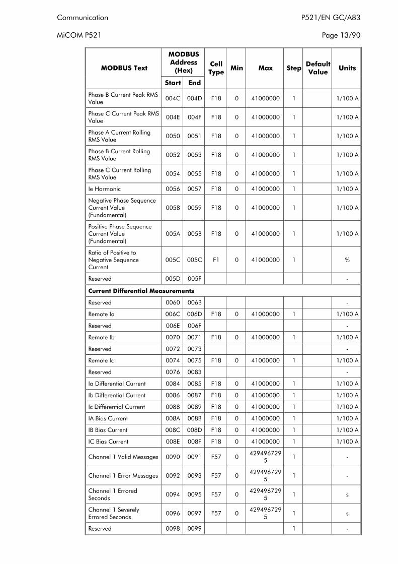
Communication P521/EN GC/A83 MiCOM P521 Page 13/90
MODBUS Address
(Hex) MODBUS Text
Start End
Cell Type Min Max Step Default
Value Units
Phase B Current Peak RMS Value
004C 004D F18 0 41000000 1 1/100 A
Phase C Current Peak RMS Value
004E 004F F18 0 41000000 1 1/100 A
Phase A Current Rolling RMS Value
0050 0051 F18 0 41000000 1 1/100 A
Phase B Current Rolling RMS Value
0052 0053 F18 0 41000000 1 1/100 A
Phase C Current Rolling RMS Value
0054 0055 F18 0 41000000 1 1/100 A
Ie Harmonic 0056 0057 F18 0 41000000 1 1/100 A
Negative Phase Sequence Current Value (Fundamental)
0058 0059 F18 0 41000000 1 1/100 A
Positive Phase Sequence Current Value (Fundamental)
005A 005B F18 0 41000000 1 1/100 A
Ratio of Positive to Negative Sequence Current
005C 005C F1 0 41000000 1 %
Reserved 005D 005F -
Current Differential Measurements
Reserved 0060 006B -
Remote Ia 006C 006D F18 0 41000000 1 1/100 A
Reserved 006E 006F -
Remote Ib 0070 0071 F18 0 41000000 1 1/100 A
Reserved 0072 0073 -
Remote Ic 0074 0075 F18 0 41000000 1 1/100 A
Reserved 0076 0083 -
Ia Differential Current 0084 0085 F18 0 41000000 1 1/100 A
Ib Differential Current 0086 0087 F18 0 41000000 1 1/100 A
Ic Differential Current 0088 0089 F18 0 41000000 1 1/100 A
IA Bias Current 008A 008B F18 0 41000000 1 1/100 A
IB Bias Current 008C 008D F18 0 41000000 1 1/100 A
IC Bias Current 008E 008F F18 0 41000000 1 1/100 A
Channel 1 Valid Messages 0090 0091 F57 0 429496729
5 1 -
Channel 1 Error Messages 0092 0093 F57 0 429496729
5 1 -
Channel 1 Errored Seconds 0094 0095 F57 0
4294967295 1 s
Channel 1 Severely Errored Seconds
0096 0097 F57 0 429496729
5 1 s
Reserved 0098 0099 1 -

P521/EN GC/A83 Communication Page 14/104 MiCOM P521
MODBUS Address
(Hex) MODBUS Text
Start End
Cell Type Min Max Step Default
Value Units
Channel 1 Propagation Delay
009A 009B F57 0 200000 1 µs
Reserved 009C 00A7 1 -
Comms. Time Elapsed 00A8 00A9 F57 0 429496729
5 1 s
Local Angle A-B 00AA 00AA F2 -180 179 1 degrees
Local Angle B-C 00AB 00AB F2 -180 179 1 degrees
Local Angle C-A 00AC 00AC F2 -180 179 1 degrees
Diff Angle A 00AD 00AD F2 -180 179 1 degrees
Diff Angle B 00AE 00AE F2 -180 179 1 degrees
Diff Angle C 00AF 00AF F2 -180 179 1 degrees
Fourier Module
Modulus IA 00B0 00B0 F1 -
Modulus IB 00B1 00B1 F1 -
Modulus IC 00B2 00B2 F1 -
Modulus IE 00B3 00B3 F1 -
Fourier Argument
Argument IA 00B4 00B4 F1 -
Argument IB 00B5 00B5 F1 -
Argument IC 00B6 00B6 F1 -
Argument IE 00B7 00B7 F1 -
Module I2 00B8 00B8 F1 -
Module I1 00B9 00B9 F1 -
Reserved 00BA 00C0 F1 -
Rolling Demand
RMS IA Average Rolling Demand
00C1 00C2 F57 0 41000000 1 1/100 A
RMS IB Average Rolling Demand
00C3 00C4 F57 0 41000000 1 1/100 A
RMS IC Average Rolling Demand
00C5 00C6 F57 0 41000000 1 1/100 A
RMS IA Peak Rolling Demand
00C7 00C8 F57 0 41000000 1 1/100 A
RMS IB Peak Rolling Demand 00C9 00CA F57 0 41000000 1 1/100 A
RMS IC Peak Rolling Demand 00CB 00CC F57 0 41000000 1 1/100 A
Inrush
Inrush Block Control Flags 00CD 00CD F70 0 FFFF 2N
Inrush Block Alarm Flags 00CE 00CE F71 0 FFFF 2N
CTS

Communication P521/EN GC/A83 MiCOM P521 Page 15/90
MODBUS Address
(Hex) MODBUS Text
Start End
Cell Type Min Max Step Default
Value Units
CTS Control Flags 00CF 00CF F72 0 FFFF 2N
CTS Alarm Flags 00D0 00D0 F73 0 FFFF 2N
Frame Mode
Frame Mode Flag 00D1 00D1 F80 0 1 1
Frame Mode Alarm Flag 00D2 00D2 F80 0 1 1
CORTEC Information
Model Number 00D3 00DA F86
Serial Number 00DB 00DE F86
Reserved 00DF 00FF -
3.3.2 Page 1: non protection settings
MODBUS Address
(Hex) MODBUS Text
Start End
Cell Type Min Max Step Default
Value Units
Remote Parameters
Address 0100 0100 F1 1 255 1 1 -
Language 0101 0101 -
Password 0102 0103 F10 65 90 1 AAAA -
Frequency 0104 0104 F1 50 60 10 50 Hz
Phase A Label 0105 0105 F25 L1 R 1 L1 -
Phase B Label 0106 0106 F25 L2 W 1 L2 -
Phase C Label 0107 0107 F25 L3 B 1 L3 -
Earth Label 0108 0108 F25 N E 1 N -
Default Display 0109 0109 F26 1 4 1 1 -
User Reference (characters 1, 2, 3 and 4)
010A 010B F10 48 90 1 MiCO -
Fault Number Selected 010C 010C F31 1 5 1 5 -
Digital Inputs Setting 010D 010D F12 0 31 1 0
Number of Instantaneous Faults to Display
010E 010E F31 1 5 1 5 -
Voltage Input Setting on the Digital Inputs 010F 010F F50 0 1 1 0 -
CB Monitoring Measurements
Operation Number 0110 0110 F1 1 -
CB Operating Time 0111 0111 F1 0 600000 1 1/100 s

P521/EN GC/A83 Communication Page 16/104 MiCOM P521
MODBUS Address
(Hex) MODBUS Text
Start End
Cell Type Min Max Step Default
Value Units
Sum of Phase A Broken CB Current Squared
0112 0113 F18 An
Sum of Phase B Broken CB Current Squared
0114 0115 F18 An
Sum of Phase C Broken CB Current Squared
0116 0117 F18 An
CB Closing Time 0118 0118 F1 0 600000 1 1/100 s
Manual CB Trip 0119 0119 F63 0 2 1 -
CB Trip Manual Delay 011A 011A F1 0 6000 100 0 1/100 s
CB Close Manual Delay 011B 011B F1 0 6000 100 0 1/100 s
Reserved 011C 011E N/A N/A N/A N/A -
Status of Output Latched Relays 011F 011F F14 0 3FF 2 N
Ratio
Primary Phase CT Value 0120 0120 F1 1 9999 1 1000 -
Secondary Phase CT Value 0121 0121 F1 1 5 4 1 -
Primary Earth CT Value 0122 0122 F1 1 9999 1 1000 -
Secondary Earth CT Value 0123 0123 F1 1 5 4 1 -
CT Ratio Correction 0124 0124 F1 50 10000 1 1000 1/1000
Vector Compensation 0125 0125 F66 0 14 1 0 -
Reserved 0126 012E -
Phase Rotation 012F 012F F51 0 1 1 0 -
Communications
Speed 0130 0130 F4 0 7 1 6 = 19200 -
Parity 0131 0131 F5 0 2 1 0 = None -
Stop Bit 0132 0132 F29 0 1 1 0= 1 stop bit -
COM Available 0133 0133 F30 0 1 1 1 = com available -
Date Format 0134 0134 F48 0 1 1 0 = Private -
Reserved 0135 013F -

Communication P521/EN GC/A83 MiCOM P521 Page 17/90
MODBUS Address
(Hex) MODBUS Text
Start End
Cell Type Min Max Step Default
Value Units
Protection Comms.
Protocol 0140 0140 F58 0 1 1 0 = SDLC -
Data Rate 0141 0141 F59 0 3 1 0 = 64 kbps -
Relay Address 0142 0142 F60 0 31 1 0 = 1A -
Clock Source Ch1 0143 0143 F61 0 1 1 0 = Internal -
Reserved 0144 0147 -
Comm Fail Timer 0148 0148 F1 0 999 1 999 1/100 s
Comm Delay Tol. 0149 014A F57 20 1000 2 1000 1/100 ms
Char Mod Time 014B 014C F57 0 10000 10 10000 1/100 s
Reserved 014D 014F -
Configuration
Comm. Fail Reset 014F 014F F1 0 1 1 0 -
Active Setting Group2 0150 0150 F1 1 2 1 1 -
Inst. Self Reset 0151 0151 F1 0 1 1 1 -
Change Group Input 0152 0152 F47 0 1 1 1 -
Reserved 0153 0153 F1 0 1 1 1 -
LEDs Allocation
Led 5 0154 0154 F19 0 FFFF 1 0 -
Led 6 0155 0155 F19 0 FFFF 1 0 -
Led 7 0156 0156 F19 0 FFFF 1 0 -
Led 8 0157 0157 F19 0 FFFF 1 0 -
Led PF 5 0158 0158 F19' 0 FFFF 1 0 -
Led PF 6 0159 0159 F19' 0 FFFF 1 0 -
Led PF 7 015A 015A F19' 0 FFFF 1 0 -
Led PF 8 015B 015B F19' 0 FFFF 1 0 -
Led PFA 5 015C 015C F19'' 0 FFFF 1 0 -
Led PFA 6 015D 015D F19'' 0 FFFF 1 0 -
Led PFA 7 015E 015E F19'' 0 FFFF 1 0 -
Led PFA 8 015F 015F F19'' 0 FFFF 1 0 -
Commissioning Options
Commissioning Options?
0160 0160 F24 0 1 1 0 = No -
2 * Note: Edge must be set in change group input.

P521/EN GC/A83 Communication Page 18/104 MiCOM P521
MODBUS Address
(Hex) MODBUS Text
Start End
Cell Type Min Max Step Default
Value Units
Led Testing 0161 0161 F24 0 1 1 0 = No -
Output Contacts 0162 0162 F24 0 1 1 0 = No -
Relays selected for Test 0163 0163 F62 0 FFFF 2N 0 -
Test Relays 0164 0164 F24 0 1 1 0 = No -
Circuit breaker Measurements 0165 0165 F24 0 1 1 0 = No -
Communications Loopback 0166 0166 F24 0 1 1 0 = No -
Logic Input Allocation
Logic Input 1 0167 0167 F15 0 FFFF 2N 0 -
Logic Input 2 0168 0168 F15 0 FFFF 2N 0 -
Logic Input 3 0169 0169 F15 0 FFFF 2N 0 -
Logic Input 4 016A 016A F15 0 FFFF 2N 0 -
Logic Input 5 016B 016B F15 0 FFFF 2N 0 -
Reserved 016C 016F -
Logic Input 1F 0170 0170 F15’ '0 FFFF 2N 0 -
Logic Input 2F 0171 0171 F15’ 0 FFFF 2N 0 -
Logic Input 3F 0172 0172 F15’ 0 FFFF 2N 0 -
Logic Input 4F 0173 0173 F15’ 0 FFFF 2N 0 -
Logic Input 5F 0174 0174 F15’ 0 FFFF 2N 0 -
Reserved 0175 0178 -
Auxiliary Timer 1 0179 0179 F1 0 20000 1 0 1/100 s
Auxiliary Timer 2 017A 017A F1 0 20000 1 0 1/100 s
Output Contact Inversion 01A4 01A4 F14 0 FFFF 2N 0 -
Reserved 01A5 017F -
Output Relay Allocation
Broken Conductor Detection 0180 0180 F14 0 FFFF 1 0 -
CB Failure 0181 0181 F14 0 FFFF 1 0 -
I< 0182 0182 F14 0 FFFF 1 0 -
I2> 0183 0183 F14 0 FFFF 1 0 -
I2>> 0184 0184 F14 0 FFFF 1 0 -
Thermal Overload Alarm 0185 0185 F14 0 FFFF 1 0 -
Thermal Overload Trip 0186 0186 F14 0 FFFF 1 0 -
tAUX1 0187 0187 F14 0 FFFF 1 0 -

Communication P521/EN GC/A83 MiCOM P521 Page 19/90
MODBUS Address
(Hex) MODBUS Text
Start End
Cell Type Min Max Step Default
Value Units
tAUX2 0188 0188 F14 0 FFFF 1 0 -
CB Close 0189 0189 F14 0 FFFF 1 0 -
CB Alarm 018A 018A F14 0 FFFF 1 0 -
Trip Circuit Supervision Failure 018B 018B F14 0 FFFF 1 0 -
Active Setting Group 018C 018C F14 0 FFFF 1 0 -
Trip 018D 018D F14 0 FFFF 1 0 -
tI> 018E 018E F14 0 FFFF 1 0 -
tI>> 018F 018F F14 0 FFFF 1 0 -
tI>>> 0190 0190 F14 0 FFFF 1 0 -
tI>>>> 0191 0191 F14 0 FFFF 1 0 -
tIe> 0192 0192 F14 0 FFFF 1 0 -
tIe>> 0193 0193 F14 0 FFFF 1 0 -
tIe>>> 0194 0194 F14 0 FFFF 1 0 -
tIe>>>> 0195 0195 F14 0 FFFF 1 0 -
I> 0196 0196 F14 0 FFFF 1 0 -
I>> 0197 0197 F14 0 FFFF 1 0 -
I>>> 0198 0198 F14 0 FFFF 1 0 -
I>>>> 0199 0199 F14 0 FFFF 1 0 -
Ie> 019A 019A F14 0 FFFF 1 0 -
Ie>> 019B 019B F14 0 FFFF 1 0 -
Ie>>> 019C 019C F14 0 FFFF 1 0 -
Ie>>>> 019D 019D F14 0 FFFF 1 0 -
Idiff 019E 019E F14 0 FFFF 1 0 -
Backup 019F 019F F14 0 FFFF 1 0 -
C fail 01A0 01A0 F14 0 FFFF 1 0 -
Direct Intertrip 01A1 01A1 F14 0 FFFF 1 0 -
C-Diff Intertrip 01A2 01A2 F14 0 FFFF 1 0 -
PIT 01A3 01A3 F14 0 FFFF 1 0 -
Reserved 01A4 01A5 -
Relay Logic
Trip 01A6 01A6 F6 0 FFFF 1 FFFF -
Trip 2 01A7 01A7 F6' 0 FFFF 1 7 -
Relay Latching 01A8 01A8 F8 0 FFFF 1 0 -
Relay Latching 2 01A9 01A9 F8' 0 FFFF 1 0 -
Blocking Logic 1 01AA 01AA F8''' 0 FFFF 1 0 -

P521/EN GC/A83 Communication Page 20/104 MiCOM P521
MODBUS Address
(Hex) MODBUS Text
Start End
Cell Type Min Max Step Default
Value Units
Blocking Logic 2 01AB 01AB F8''' 0 FFFF 1 0 -
Broken Conductor Detection
Broken Conductor Detection 01AC 01AC F24 0 1 0.44 0 -
TBC 01AD 01AD F1 5 14400 1 5 s
I2/I1 Threshold 01AE 01AE F1 20 100 1 20 %
Cold Load Start
Cold Load Start 01AF 01AF F24 0 1 1 0 -
Cold Load Start Thresholds 01B0 01B0 F33 0 FFFF 1 0 -
Cold Load Start % 01B1 01B1 F1 20 500 1 200 %
Cold Load Start Delay 01B2 01B2 F1 1 36000 1 400 1/10s
Selective Scheme Logic
Selective Scheme Logic 1 01B3 01B3 F40 0 FFFF 1 0 -
tSEL1 01B4 01B4 F1 0 15000 1 0 1/100 s
Selective Scheme Logic 2 01B5 01B5 F40 0 FFFF 1 0 -
tSEL2 01B6 01B6 F1 0 15000 1 0 1/100 s
Reserved 01B7 01BF -
Selective Intertripping
Direct Intertrip 01B7 01B7 F67 0 FFFF 1 0 -
Reserved 01B8 01BF -
Disturbance
Pre-Time 01C0 01C0 F1 1 90 1 1 1/10 s
Reserved 01C1 01C1
Disturbance Starting Condition 01C2 01C2 F32 0 1 1 1 =
on trip -
Circuit Breaker Supervision
TC Supervision? 01C3 01C3 F24 0 1 1 0 -
t Trip Circuit 01C4 01C4 F1 10 10000 5 40 1/100s
CB Open Supervision? 01C5 01C5 F24 0 1 1 0 -
CB Open Time 01C6 01C6 F1 5 100 5 5 1/100s
CB Close Supervision? 01C7 01C7 F24 0 1 1 0 -
CB Close Time 01C8 01C8 F1 5 100 5 5 1/100s
CB Open Alarm? 01C9 01C9 F1 0 1 2 0 -
CB Open NB 01CA 01CA F1 0 50000 1 0 -

Communication P521/EN GC/A83 MiCOM P521 Page 21/90
MODBUS Address
(Hex) MODBUS Text
Start End
Cell Type Min Max Step Default
Value Units
Sum Amps (n)? 01CB 01CB F24 0 1 1 0 -
Sum Amps (n) 01CC 01CC F1 0 4000 1 0 MA^n
N 01CD 01CD F1 1 2 1 1 -
t Open Pulse 01CE 01CE F1 10 500 5 10 1/100 s
t Close Pulse 01CF 01CF F1 10 500 5 10 1/100 s
Time Peak Value
Peak Value 01D0 01D0 F42 5 60 TI 5 Min
CB Fail
CB Failure 01D1 01D1 F24 0 1 1 0 -
I< 01D2 01D2 F1 2 100 1 10 1/100In
TBF 01D3 01D3 F1 3 1000 1 10 1/100s
Block Instantaneous Phase 01D4 01D4 F24 0 1 1 0 = No -
Block Instantaneous Earth 01D5 01D5 F24 0 1 1 0 = No -
Rolling Demand
Rolling Sub Periods 01D6 01D6 F1 1 60 1 5 MN
Number of Sub Periods 01D7 01D7 F1 1 24 1 1 -
Non Protection Settings - Output Relay Allocation (Addtional)
Equation A 01D8 01D8 F14 0 FFFF 2N -
Equation B 01D9 01D9 F14 0 FFFF 2N
Equation C 01DA 01DA F14 0 FFFF 2N
Equation D 01DB 01DB F14 0 FFFF 2N
Equation E 01DC 01DC F14 0 FFFF 2N
Equation F 01DD 01DD F14 0 FFFF 2N
Equation G 01DE 01DE F14 0 FFFF 2N
Equation H 01DF 01DF F14 0 FFFF 2N
Input 1 01E0 01E0 F14 0 FFFF 2N
Input 2 01E1 01E1 F14 0 FFFF 2N
Input 3 01E2 01E2 F14 0 FFFF 2N
Input 4 01E3 01E3 F14 0 FFFF 2N
Input 5 01E4 01E4 F14 0 FFFF 2N
Programmable Intertrip A 01E5 01E5 F14 0 FFFF 2N
Programmable Intertrip B 01E6 01E6 F14 0 FFFF 2N

P521/EN GC/A83 Communication Page 22/104 MiCOM P521
MODBUS Address
(Hex) MODBUS Text
Start End
Cell Type Min Max Step Default
Value Units
Programmable Intertrip C 01E7 01E7 F14 0 FFFF 2N
Programmable Intertrip D 01E8 01E8 F14 0 FFFF 2N
CTS local CT Alarm 01E9 01E9 F14 0 FFFF 2N
CTS remote CT Alarm 01EA 01EA F14 0 FFFF 2N
CTS Block 01EB 01EB F14 0 FFFF 2N
CTS Cdiff Restrain 01EC 01EC F14 0 FFFF 2N
Convention Mode 01ED 01ED F14 0 FFFF 2N
Non Protection Settings -Block Allocation (Addtional)
Blocking Logic 1 Function Allocation (Word 2)
01EE 01EE F8” 0 FFFF 2N
Blocking Logic 2 Function Allocation (Word 2)
01EF 01EF F8” 0 FFFF 2N
Non Protection Settings - LED Allocation (Addtional)
LED 5 Function Allocation (Word 4) 01F0 01F0 F19” 0 FFFF 2N
LED 6 Function Allocation (Word 4) 01F1 01F1 F19” 0 FFFF 2N
LED 7 Function Allocation (Word 4) 01F2 01F2 F19” 0 FFFF 2N
LED 8 Function Allocation (Word 4) 01F3 01F3 F19” 0 FFFF 2N
Non Protection Settings - Record (Addtional)
Disturb Trigger 01F4 01F4 F24 0 1 1
Frame Mode 01F5 01F5 F80 0 1 1
Record Number 01F6 01F6 F1 1 5 1
Non Protection Settings - Configuration (Addtional)
Diff Disable Alarm 01F7 01F7 F24 0 1 1
Non Protection Settings - Output Relay Allocation (Addtional2)
Diff Disable (Output Relay Allocation) 01F8 01F8 F14 0 FFFF 2N
Reserved 01F9 01FF

Communication P521/EN GC/A83 MiCOM P521 Page 23/90
3.3.3 Page 2h: group 1 protection settings
MODBUS Address
(Hex) MODBUS Text
Start End
Cell Type Min Max Step Default
Value Units
Setting Group 1
Current Differential
Current Diff.? 0200 0200 F24 0 1 1 1 = Yes -
Is1 0201 0201 F1 10 200 2 20 1/100
Is2 0202 0202 F1 100 3000 5 200 1/100
K1 0203 0203 F1 0 150 5 30 %
K2 0204 0204 F1 30 150 5 150 %
Time Delay Type 0205 0205 F27 0 1 1 0 = DMT
tIdiff Value 0206 0206 F1 0 15000 1 0 1/100s
IDMT Curve Type 0207 0207 F3 0 9 1 1 = SI -
TMS 0208 0208 F1 25 1500 25 1000 1/1000
Time Dial 0209 020A F57 100 100000 100 100 1/1000
PIT Time 020B 020B F1 0 200 1 20 1/100s
PIT I Disable 020C 020C F24 0 1 1 0 -
PIT I Selection 0270 0270 F68 0 1 1 0 -
PIT I Threshold 0271 0271 F1 10 4000 1 20 1/100 In
PIT OC Stages 0272 0272 F69 0 FFFF 2N 0 -
Inrush Restraint 020D 020D F24 0 1 1 0 -
Transient Bias 0273 0273 F24 0 1 1 0 -
DIT Alarm 0274 0274 F24 0 1 1 1 -
PIT Alarm 0275 0275 F24 0 1 1 1 -
Rx DIT Dwell Time 020E 020E F1 10 500 0 10 1/100s
IDiff High Set 020F 020F F1 400 3200 1 400 1/100 In
Kr 0276 0276 F1 3 20 1 4
Reserved 0277 02FF -
Overcurrent
I> 0210 0210 F24 0 2 1 0 = No -
I> Threshold 0211 0211 F1 10 2500 1 100 1/100 In
I> Delay Type 0212 0212 F27 0 2 1 0 = DMT -
I> Curve Type 0213 0213 F3 0 9 1 1 = SI -
I> TMS Value 0214 0214 F1 25 1500 25 1000 1/1000
t> TD Value 0215 0216 F57 100 100000 100 1000 1/1000
I> K Value (RI Curve) 0217 0217 F1 100 10000 5 100 1/1000s
tI> Value 0218 0218 F1 0 15000 1 4 1/100s
I> Reset Type 0219 0219 F27 0 1 1 0 -

P521/EN GC/A83 Communication Page 24/104 MiCOM P521
MODBUS Address
(Hex) MODBUS Text
Start End
Cell Type Min Max Step Default
Value Units
I> RTMS Value 021A 021A F1 25 3200 25 25 1/1000
I> tRESET Value 021B 021B F1 4 10000 1 4 1/100 s
I>> 021C 021C F24 0 2 1 0 = No -
I>> Threshold 021D 021D F1 50 4000 5 100 1/100 In
I>> Delay Type 021E 021E F27 0 2 1 0 = DMT -
I>> Curve Type 021F 021F F3 0 9 1 1 = SI -
I>> TMS Value 0220 0220 F1 25 1500 25 1000 1/1000
I>> TD Value 0221 0222 F57 100 100000 100 100 1/1000
I>> K Value (RI Curve) 0223 0223 F1 100 10000 5 100 1/1000
tI>> Value 0224 0224 F1 0 15000 1 4 1/100 s
I>> Reset Type 0225 0225 F27 0 1 1 0 -
I>> RTMS Value 0226 0226 F1 25 3200 25 25 1/1000
I>> tRESET Value 0227 0227 F1 4 10000 1 4 1/100s
I>>> 0228 0228 F24 0 2 1 0 = No -
I>>> Value 0229 0229 F1 50 4000 5 2000 1/100 In
tI>>> Value 022A 022A F1 0 15000 1 1 1/100 s
I>>>> 022B 022B F24 0 2 1 0 = No -
I>>>> Value 022C 022C F1 50 4000 5 2000 1/100
tI>>>> Value 022D 022D F1 0 15000 1 1 1/100 s
Ie> 022E 022E F24 0 2 1 0 = No -
Ie> Value (Normal) 022F 022F F1 10 2500 1 10 1/100 Ion
Ie> Value (Sensitive) 022F 022F F1 10 1000 5 10 1/1000 Ion
Ie> Value (V. Sensitive) 022F 022F F1 2 1000 1 2 1/1000
Ion
Ie> Time Delay Type 0230 0230 F27 0 3 1 0 = DMT -
Ie> IDMT Curve Type 0231 0231 F3 0 9 1 1 = SI -
Ie> TMS Value 0232 0232 F1 25 1500 25 1000 1/1000
Ie> TD Value 0233 0234 F57 100 100000 100 100 1/1000
Ie> K Value RI Curve) 0235 0235 F1 100 10000 5 100 1/1000
tIe> Value 0236 0236 F1 0 15000 1 4 1/100
Ie> Reset Type 0237 0237 F27 0 1 1 0 = DMT -
Ie> RTMS Value 0238 0238 F1 25 3200 25 25 1/1000
Ie> tRESET Value 0239 0239 F1 4 10000 1 4 1/100s

Communication P521/EN GC/A83 MiCOM P521 Page 25/90
MODBUS Address
(Hex) MODBUS Text
Start End
Cell Type Min Max Step Default
Value Units
Ie> Laborlec 023A 023A F3' 0 2 1 0 = Curve 1 -
Ie>> 023B 023B F24 0 2 1 0 = No -
Ie>> Value (Normal) 023C 023C F1 50 4000 1 100 1/100 Ion
Ie>> Value (Sensitive) 023C 023C F1 10 8000 5 100 1/1000 Ion
Ie>> Value (V. Sensitive) 023C 023C F1 2 1000 1 100 1/1000
Ion
Ie>> Time Delay Type 023D 023D F1 0 3 1 0 =DMT -
Ie>> IDMT Curve Type 023E 023E F3 0 9 1 1 = SI -
Ie>> TMS Value 023F 023F F1 25 1500 25 1000 1/1000
Ie>> TD Value 0240 0241 F57 100 100000 100 100 1/1000
Ie>> K Value (RI Curve) 0242 0242 F1 100 10000 5 100 1/1000
tIe>> Value 0243 0243 F1 0 15000 1 1 1/100
Ie>> Reset Type 0244 0244 F27 0 1 1 0 = DMT -
Ie>> RTMS Value 0245 0245 F1 25 3200 25 25 1/1000
Ie>> tRESET Value 0246 0246 F1 4 10000 1 4 1/100s
Ie>>Laborlec 0247 0247 F3' 0 2 1 0 = Curve 1 -
Ie>>> 0248 0248 F24 0 2 1 0 = No -
Ie>>> Value (Normal) 0249 0249 F1 50 4000 1 100 1/100 Ion
Ie>>> Value (Sensitive) 0249 0249 F1 10 8000 5 100 1/1000
Ion
Ie>>> Value (V. Sensitive) 0249 0249 F1 2 1000 1 100 1/1000
Ion
tIe>>> Value 024A 024A F1 0 15000 1 1 1/100
Ie>>>> 024B 024B F24 0 2 1 0 = No -
Ie>>>> Value (Normal) 024C 024C F1 50 4000 1 100 1/100 Ion
Ie>>>> Value (Sensitive) 024C 024C F1 10 8000 5 100 1/1000
Ion
Ie>>>> Value (V. Sensitive) 024C 024C F1 2 1000 1 100 1/1000
Ion
tIe>>>> Value 024D 024D F1 0 15000 1 1 1/100
Thermal
Ith> 024E 024E F24 0 1 1 0 = No -
Ith> Value 024F 024F F1 10 320 1 100 1/100

P521/EN GC/A83 Communication Page 26/104 MiCOM P521
MODBUS Address
(Hex) MODBUS Text
Start End
Cell Type Min Max Step Default
Value Units
Reserved 0250 0250 -
Ith> K Value 0251 0251 F1 100 150 1 105 1/100 %
Ith> Trip Threshold 0252 0252 F1 50 200 1 100 -
Ith> Alarm 0253 0253 F24 0 1 1 0 = No -
Ith> Alarm Threshold 0254 0254 F1 50 200 1 90 %
Te1 0255 0255 F1 1 200 1 1 Mn
Reserved 0256 0256
Negative sequence
I2> 0257 0257 F24 0 1 1 0 = No -
I2> Threshold 0258 0258 F1 10 4000 1 100 In/100
I2> Delay Type 0259 0259 F27 0 2 1 0 = DMT -
I2> Curve 025A 025A F3 0 9 1 1 = SI -
I2> TMS Value 025B 025B F1 25 1500 25 1000 1/1000
I2> TD Value 25C 025D F57 100 100000 100 100 1/1000
I2> K Value (RI) 025E 025E F1 100 10000 5 100 1/1000
tI2> Value 025F 025F F1 0 15000 1 0 1/100s
I2> Reset Type 0260 0260 F27 0 1 1 0 = DMT -
I2> RTMS Value 0261 0261 F1 25 3200 25 25 1/1000
I2> tRESET Value 0262 0262 F1 4 10000 1 4 1/100 s
I2>> 0263 0263 F27 0 1 1 0 = No -
I2>> Threshold 0264 0264 F1 10 4000 1 100 1/100
tI2>> 0265 0265 F1 0 15000 1 0 1/100s
Undercurrent
I< 0266 0266 F24 0 1 1 0 = No -
I< Threshold 0267 0267 F1 2 100 1 20 1/100
tI2< Value 0268 0268 F1 0 15000 1 0 1/100
Reserved 0269 02FF -
Protection Settings - Current Differential (Additional)
Harmonic Ratio 0277 0277 F1 5 50 1 1%
Reserved 0278 0278
CTS Is1 0279 0279 F1 20 400 5 1/100 In
Reserved 027A 02FF

Communication P521/EN GC/A83 MiCOM P521 Page 27/90
3.3.4 Page 4h: remote control words
MODBUS Address
(Hex) MODBUS Text
Start End
Cell Type Min Max Step Default
Value Units
Remote Control
Remote Control Word 1 0400 0400 F9 0 31 1 0 -
Reserved 0401 0401 N/A N/A N/A N/A -
Reserved 0402 0402 N/A N/A N/A N/A -
Remote Control Word 3 0403 0403 F46 0 511 1 0 -
3.3.5 Pages 5h: Boolean Equation
MODBUS Address
(Hex) MODBUS Text
Start End
Cell Type Min Max Step Default
Value Units
Boolean Equation
Equation A Operator 0 0500 0500 F84 0 3 1 0 -
Equation A Operator 0 0501 0501 F83 0 61 1 0 -
Equation A Operator 1 0502 0502 F84 0 3 1 0 -
Equation A Operator 1 0503 0503 F83 0 61 1 0 -
Equation A Operator 2 0504 0504 F84 0 3 1 0 -
Equation A Operator 2 0505 0505 F83 0 61 1 0 -
Equation A Operator 3 0506 0506 F84 0 3 1 0 -
Equation A Operator 3 0507 0507 F83 0 61 1 0 -
Equation A Operator 4 0508 0508 F84 0 3 1 0 -
Equation A Operator 4 0509 0509 F83 0 61 1 0 -
Equation A Operator 5 050A 050A F84 0 3 1 0 -
Equation A Operator 5 050B 050B F83 0 61 1 0 -
Equation A Operator 6 050C 050C F84 0 3 1 0 -
Equation A Operator 6 050D 050D F83 0 61 1 0 -
Equation A Operator 7 050E 050E F84 0 3 1 0 -
Equation A Operator 7 050F 050F F83 0 61 1 0 -
Equation A Operator 8 0510 0510 F84 0 3 1 0 -
Equation A Operator 8 0511 0511 F83 0 61 1 0 -
Equation A Operator 9 0512 0512 F84 0 3 1 0 -
Equation A Operator 9 0513 0513 F83 0 61 1 0 -
Equation A Operator 10 0514 0514 F84 0 3 1 0 -
Equation A Operator 10 0515 0515 F83 0 61 1 0 -

P521/EN GC/A83 Communication Page 28/104 MiCOM P521
MODBUS Address
(Hex) MODBUS Text
Start End
Cell Type Min Max Step Default
Value Units
Equation A Operator 11 0516 0516 F84 0 3 1 0 -
Equation A Operator 11 0517 0517 F83 0 61 1 0 -
Equation A Operator 12 0518 0518 F84 0 3 1 0 -
Equation A Operator 12 0519 0519 F83 0 61 1 0 -
Equation A Operator 13 051A 051A F84 0 3 1 0 -
Equation A Operator 13 051B 051B F83 0 61 1 0 -
Equation A Operator 14 051C 051C F84 0 3 1 0 -
Equation A Operator 14 051D 051D F83 0 61 1 0 -
Equation A Operator 15 051E 051E F84 0 3 1 0 -
Equation A Operator 15 051F 051F F83 0 61 1 0 -
Equation B Operator 0 0520 0520 F84 0 3 1 0 -
Equation B Operator 0 0521 0521 F83 0 61 1 0 -
Equation B Operator 1 0522 0522 F84 0 3 1 0 -
Equation B Operator 1 0523 0523 F83 0 61 1 0 -
Equation B Operator 2 0524 0524 F84 0 3 1 0 -
Equation B Operator 2 0525 0525 F83 0 61 1 0 -
Equation B Operator 3 0526 0526 F84 0 3 1 0 -
Equation B Operator 3 0527 0527 F83 0 61 1 0 -
Equation B Operator 4 0528 0528 F84 0 3 1 0 -
Equation B Operator 4 0529 0529 F83 0 61 1 0 -
Equation B Operator 5 052A 052A F84 0 3 1 0 -
Equation B Operator 5 052B 052B F83 0 61 1 0 -
Equation B Operator 6 052C 052C F84 0 3 1 0 -
Equation B Operator 6 052D 052D F83 0 61 1 0 -
Equation B Operator 7 052E 052E F84 0 3 1 0 -
Equation B Operator 7 052F 052F F83 0 61 1 0 -
Equation B Operator 8 0530 0530 F84 0 3 1 0 -
Equation B Operator 8 0531 0531 F83 0 61 1 0 -
Equation B Operator 9 0532 0532 F84 0 3 1 0 -
Equation B Operator 9 0533 0533 F83 0 61 1 0 -
Equation B Operator 10 0534 0534 F84 0 3 1 0 -
Equation B Operator 10 0535 0535 F83 0 61 1 0 -
Equation B Operator 11 0536 0536 F84 0 3 1 0 -
Equation B Operator 11 0537 0537 F83 0 61 1 0 -
Equation B Operator 12 0538 0538 F84 0 3 1 0 -
Equation B Operator 12 0539 0539 F83 0 61 1 0 -

Communication P521/EN GC/A83 MiCOM P521 Page 29/90
MODBUS Address
(Hex) MODBUS Text
Start End
Cell Type Min Max Step Default
Value Units
Equation B Operator 13 053A 053A F84 0 3 1 0 -
Equation B Operator 13 053B 053B F83 0 61 1 0 -
Equation B Operator 14 053C 053C F84 0 3 1 0 -
Equation B Operator 14 053D 053D F83 0 61 1 0 -
Equation B Operator 15 053E 053E F84 0 3 1 0 -
Equation B Operator 15 053F 053F F83 0 61 1 0 -
Equation C Operator 0 0540 0540 F84 0 3 1 0 -
Equation C Operator 0 0541 0541 F83 0 61 1 0 -
Equation C Operator 1 0542 0542 F84 0 3 1 0 -
Equation C Operator 1 0543 0543 F83 0 61 1 0 -
Equation C Operator 2 0544 0544 F84 0 3 1 0 -
Equation C Operator 2 0545 0545 F83 0 61 1 0 -
Equation C Operator 3 0546 0546 F84 0 3 1 0 -
Equation C Operator 3 0547 0547 F83 0 61 1 0 -
Equation C Operator 4 0548 0548 F84 0 3 1 0 -
Equation C Operator 4 0549 0549 F83 0 61 1 0 -
Equation C Operator 5 054A 054A F84 0 3 1 0 -
Equation C Operator 5 054B 054B F83 0 61 1 0 -
Equation C Operator 6 054C 054C F84 0 3 1 0 -
Equation C Operator 6 054D 054D F83 0 61 1 0 -
Equation C Operator 7 054E 054E F84 0 3 1 0 -
Equation C Operator 7 054F 054F F83 0 61 1 0 -
Equation C Operator 8 0550 0550 F84 0 3 1 0 -
Equation C Operator 8 0551 0551 F83 0 61 1 0 -
Equation C Operator 9 0552 0552 F84 0 3 1 0 -
Equation C Operator 9 0553 0553 F83 0 61 1 0 -
Equation C Operator 10 0554 0554 F84 0 3 1 0 -
Equation C Operator 10 0555 0555 F83 0 61 1 0 -
Equation C Operator 11 0556 0556 F84 0 3 1 0 -
Equation C Operator 11 0557 0557 F83 0 61 1 0 -
Equation C Operator 12 0558 0558 F84 0 3 1 0 -
Equation C Operator 12 0559 0559 F83 0 61 1 0 -
Equation C Operator 13 055A 055A F84 0 3 1 0 -
Equation C Operator 13 055B 055B F83 0 61 1 0 -
Equation C Operator 14 055C 055C F84 0 3 1 0 -
Equation C Operator 14 055D 055D F83 0 61 1 0 -

P521/EN GC/A83 Communication Page 30/104 MiCOM P521
MODBUS Address
(Hex) MODBUS Text
Start End
Cell Type Min Max Step Default
Value Units
Equation C Operator 15 055E 055E F84 0 3 1 0 -
Equation C Operator 15 055F 055F F83 0 61 1 0 -
Equation D Operator 0 0560 0560 F84 0 3 1 0 -
Equation D Operator 0 0561 0561 F83 0 61 1 0 -
Equation D Operator 1 0562 0562 F84 0 3 1 0 -
Equation D Operator 1 0563 0563 F83 0 61 1 0 -
Equation D Operator 2 0564 0564 F84 0 3 1 0 -
Equation D Operator 2 0565 0565 F83 0 61 1 0 -
Equation D Operator 3 0566 0566 F84 0 3 1 0 -
Equation D Operator 3 0567 0567 F83 0 61 1 0 -
Equation D Operator 4 0568 0568 F84 0 3 1 0 -
Equation D Operator 4 0569 0569 F83 0 61 1 0 -
Equation D Operator 5 056A 056A F84 0 3 1 0 -
Equation D Operator 5 056B 056B F83 0 61 1 0 -
Equation D Operator 6 056C 056C F84 0 3 1 0 -
Equation D Operator 6 056D 056D F83 0 61 1 0 -
Equation D Operator 7 056E 056E F84 0 3 1 0 -
Equation D Operator 7 056F 056F F83 0 61 1 0 -
Equation D Operator 8 0570 0570 F84 0 3 1 0 -
Equation D Operator 8 0571 0571 F83 0 61 1 0 -
Equation D Operator 9 0572 0572 F84 0 3 1 0 -
Equation D Operator 9 0573 0573 F83 0 61 1 0 -
Equation D Operator 10 0574 0574 F84 0 3 1 0 -
Equation D Operator 10 0575 0575 F83 0 61 1 0 -
Equation D Operator 11 0576 0576 F84 0 3 1 0 -
Equation D Operator 11 0577 0577 F83 0 61 1 0 -
Equation D Operator 12 0578 0578 F84 0 3 1 0 -
Equation D Operator 12 0579 0579 F83 0 61 1 0 -
Equation D Operator 13 057A 057A F84 0 3 1 0 -
Equation D Operator 13 057B 057B F83 0 61 1 0 -
Equation D Operator 14 057C 057C F84 0 3 1 0 -
Equation D Operator 14 057D 057D F83 0 61 1 0 -
Equation D Operator 15 057E 057E F84 0 3 1 0 -
Equation D Operator 15 057F 057F F83 0 61 1 0 -
Equation E Operator 0 0580 0580 F84 0 3 1 0 -
Equation E Operator 0 0581 0581 F83 0 61 1 0 -

Communication P521/EN GC/A83 MiCOM P521 Page 31/90
MODBUS Address
(Hex) MODBUS Text
Start End
Cell Type Min Max Step Default
Value Units
Equation E Operator 1 0582 0582 F84 0 3 1 0 -
Equation E Operator 1 0583 0583 F83 0 61 1 0 -
Equation E Operator 2 0584 0584 F84 0 3 1 0 -
Equation E Operator 2 0585 0585 F83 0 61 1 0 -
Equation E Operator 3 0586 0586 F84 0 3 1 0 -
Equation E Operator 3 0587 0587 F83 0 61 1 0 -
Equation E Operator 4 0588 0588 F84 0 3 1 0 -
Equation E Operator 4 0589 0589 F83 0 61 1 0 -
Equation E Operator 5 058A 058A F84 0 3 1 0 -
Equation E Operator 5 058B 058B F83 0 61 1 0 -
Equation E Operator 6 058C 058C F84 0 3 1 0 -
Equation E Operator 6 058D 058D F83 0 61 1 0 -
Equation E Operator 7 058E 058E F84 0 3 1 0 -
Equation E Operator 7 058F 058F F83 0 61 1 0 -
Equation E Operator 8 0590 0590 F84 0 3 1 0 -
Equation E Operator 8 0591 0591 F83 0 61 1 0 -
Equation E Operator 9 0592 0592 F84 0 3 1 0 -
Equation E Operator 9 0593 0593 F83 0 61 1 0 -
Equation E Operator 10 0594 0594 F84 0 3 1 0 -
Equation E Operator 10 0595 0595 F83 0 61 1 0 -
Equation E Operator 11 0596 0596 F84 0 3 1 0 -
Equation E Operator 11 0597 0597 F83 0 61 1 0 -
Equation E Operator 12 0598 0598 F84 0 3 1 0 -
Equation E Operator 12 0599 0599 F83 0 61 1 0 -
Equation E Operator 13 059A 059A F84 0 3 1 0 -
Equation E Operator 13 059B 059B F83 0 61 1 0 -
Equation E Operator 14 059C 059C F84 0 3 1 0 -
Equation E Operator 14 059D 059D F83 0 61 1 0 -
Equation E Operator 15 059E 059E F84 0 3 1 0 -
Equation E Operator 15 059F 059F F83 0 61 1 0 -
Equation F Operator 0 05A0 05A0 F84 0 3 1 0 -
Equation F Operator 0 05A1 05A1 F83 0 61 1 0 -
Equation F Operator 1 05A2 05A2 F84 0 3 1 0 -
Equation F Operator 1 05A3 05A3 F83 0 61 1 0 -
Equation F Operator 2 05A4 05A4 F84 0 3 1 0 -
Equation F Operator 2 05A5 05A5 F83 0 61 1 0 -
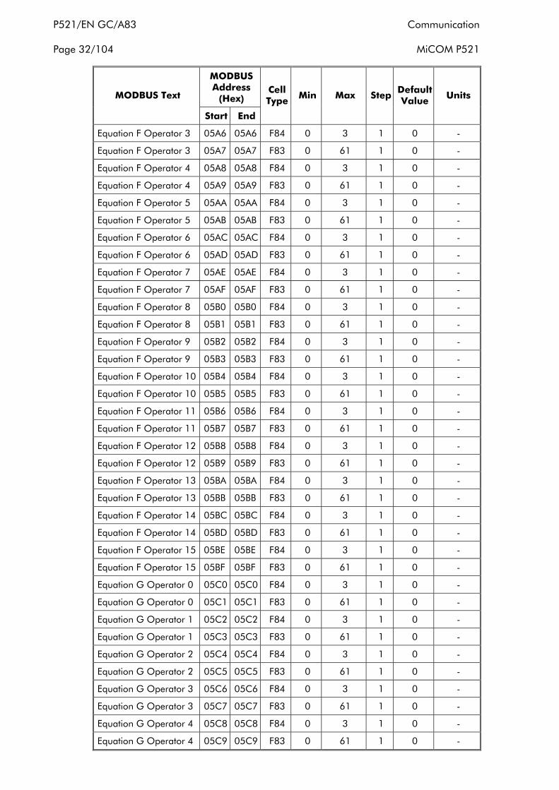
P521/EN GC/A83 Communication Page 32/104 MiCOM P521
MODBUS Address
(Hex) MODBUS Text
Start End
Cell Type Min Max Step Default
Value Units
Equation F Operator 3 05A6 05A6 F84 0 3 1 0 -
Equation F Operator 3 05A7 05A7 F83 0 61 1 0 -
Equation F Operator 4 05A8 05A8 F84 0 3 1 0 -
Equation F Operator 4 05A9 05A9 F83 0 61 1 0 -
Equation F Operator 5 05AA 05AA F84 0 3 1 0 -
Equation F Operator 5 05AB 05AB F83 0 61 1 0 -
Equation F Operator 6 05AC 05AC F84 0 3 1 0 -
Equation F Operator 6 05AD 05AD F83 0 61 1 0 -
Equation F Operator 7 05AE 05AE F84 0 3 1 0 -
Equation F Operator 7 05AF 05AF F83 0 61 1 0 -
Equation F Operator 8 05B0 05B0 F84 0 3 1 0 -
Equation F Operator 8 05B1 05B1 F83 0 61 1 0 -
Equation F Operator 9 05B2 05B2 F84 0 3 1 0 -
Equation F Operator 9 05B3 05B3 F83 0 61 1 0 -
Equation F Operator 10 05B4 05B4 F84 0 3 1 0 -
Equation F Operator 10 05B5 05B5 F83 0 61 1 0 -
Equation F Operator 11 05B6 05B6 F84 0 3 1 0 -
Equation F Operator 11 05B7 05B7 F83 0 61 1 0 -
Equation F Operator 12 05B8 05B8 F84 0 3 1 0 -
Equation F Operator 12 05B9 05B9 F83 0 61 1 0 -
Equation F Operator 13 05BA 05BA F84 0 3 1 0 -
Equation F Operator 13 05BB 05BB F83 0 61 1 0 -
Equation F Operator 14 05BC 05BC F84 0 3 1 0 -
Equation F Operator 14 05BD 05BD F83 0 61 1 0 -
Equation F Operator 15 05BE 05BE F84 0 3 1 0 -
Equation F Operator 15 05BF 05BF F83 0 61 1 0 -
Equation G Operator 0 05C0 05C0 F84 0 3 1 0 -
Equation G Operator 0 05C1 05C1 F83 0 61 1 0 -
Equation G Operator 1 05C2 05C2 F84 0 3 1 0 -
Equation G Operator 1 05C3 05C3 F83 0 61 1 0 -
Equation G Operator 2 05C4 05C4 F84 0 3 1 0 -
Equation G Operator 2 05C5 05C5 F83 0 61 1 0 -
Equation G Operator 3 05C6 05C6 F84 0 3 1 0 -
Equation G Operator 3 05C7 05C7 F83 0 61 1 0 -
Equation G Operator 4 05C8 05C8 F84 0 3 1 0 -
Equation G Operator 4 05C9 05C9 F83 0 61 1 0 -
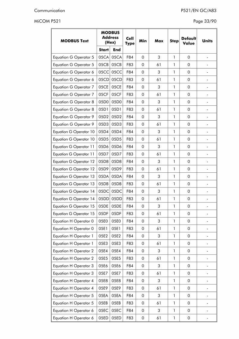
Communication P521/EN GC/A83 MiCOM P521 Page 33/90
MODBUS Address
(Hex) MODBUS Text
Start End
Cell Type Min Max Step Default
Value Units
Equation G Operator 5 05CA 05CA F84 0 3 1 0 -
Equation G Operator 5 05CB 05CB F83 0 61 1 0 -
Equation G Operator 6 05CC 05CC F84 0 3 1 0 -
Equation G Operator 6 05CD 05CD F83 0 61 1 0 -
Equation G Operator 7 05CE 05CE F84 0 3 1 0 -
Equation G Operator 7 05CF 05CF F83 0 61 1 0 -
Equation G Operator 8 05D0 05D0 F84 0 3 1 0 -
Equation G Operator 8 05D1 05D1 F83 0 61 1 0 -
Equation G Operator 9 05D2 05D2 F84 0 3 1 0 -
Equation G Operator 9 05D3 05D3 F83 0 61 1 0 -
Equation G Operator 10 05D4 05D4 F84 0 3 1 0 -
Equation G Operator 10 05D5 05D5 F83 0 61 1 0 -
Equation G Operator 11 05D6 05D6 F84 0 3 1 0 -
Equation G Operator 11 05D7 05D7 F83 0 61 1 0 -
Equation G Operator 12 05D8 05D8 F84 0 3 1 0 -
Equation G Operator 12 05D9 05D9 F83 0 61 1 0 -
Equation G Operator 13 05DA 05DA F84 0 3 1 0 -
Equation G Operator 13 05DB 05DB F83 0 61 1 0 -
Equation G Operator 14 05DC 05DC F84 0 3 1 0 -
Equation G Operator 14 05DD 05DD F83 0 61 1 0 -
Equation G Operator 15 05DE 05DE F84 0 3 1 0 -
Equation G Operator 15 05DF 05DF F83 0 61 1 0 -
Equation H Operator 0 05E0 05E0 F84 0 3 1 0 -
Equation H Operator 0 05E1 05E1 F83 0 61 1 0 -
Equation H Operator 1 05E2 05E2 F84 0 3 1 0 -
Equation H Operator 1 05E3 05E3 F83 0 61 1 0 -
Equation H Operator 2 05E4 05E4 F84 0 3 1 0 -
Equation H Operator 2 05E5 05E5 F83 0 61 1 0 -
Equation H Operator 3 05E6 05E6 F84 0 3 1 0 -
Equation H Operator 3 05E7 05E7 F83 0 61 1 0 -
Equation H Operator 4 05E8 05E8 F84 0 3 1 0 -
Equation H Operator 4 05E9 05E9 F83 0 61 1 0 -
Equation H Operator 5 05EA 05EA F84 0 3 1 0 -
Equation H Operator 5 05EB 05EB F83 0 61 1 0 -
Equation H Operator 6 05EC 05EC F84 0 3 1 0 -
Equation H Operator 6 05ED 05ED F83 0 61 1 0 -
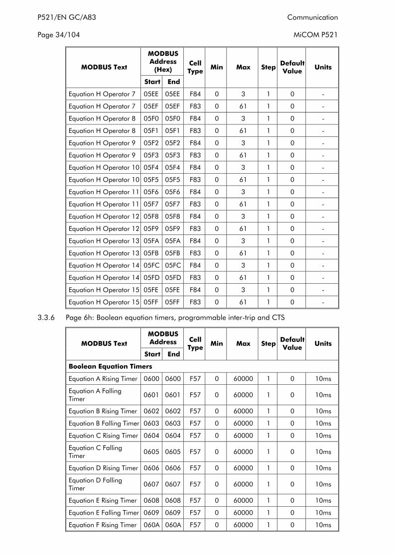
P521/EN GC/A83 Communication Page 34/104 MiCOM P521
MODBUS Address
(Hex) MODBUS Text
Start End
Cell Type Min Max Step Default
Value Units
Equation H Operator 7 05EE 05EE F84 0 3 1 0 -
Equation H Operator 7 05EF 05EF F83 0 61 1 0 -
Equation H Operator 8 05F0 05F0 F84 0 3 1 0 -
Equation H Operator 8 05F1 05F1 F83 0 61 1 0 -
Equation H Operator 9 05F2 05F2 F84 0 3 1 0 -
Equation H Operator 9 05F3 05F3 F83 0 61 1 0 -
Equation H Operator 10 05F4 05F4 F84 0 3 1 0 -
Equation H Operator 10 05F5 05F5 F83 0 61 1 0 -
Equation H Operator 11 05F6 05F6 F84 0 3 1 0 -
Equation H Operator 11 05F7 05F7 F83 0 61 1 0 -
Equation H Operator 12 05F8 05F8 F84 0 3 1 0 -
Equation H Operator 12 05F9 05F9 F83 0 61 1 0 -
Equation H Operator 13 05FA 05FA F84 0 3 1 0 -
Equation H Operator 13 05FB 05FB F83 0 61 1 0 -
Equation H Operator 14 05FC 05FC F84 0 3 1 0 -
Equation H Operator 14 05FD 05FD F83 0 61 1 0 -
Equation H Operator 15 05FE 05FE F84 0 3 1 0 -
Equation H Operator 15 05FF 05FF F83 0 61 1 0 -
3.3.6 Page 6h: Boolean equation timers, programmable inter-trip and CTS
MODBUS Address MODBUS Text
Start End
Cell Type Min Max Step Default
Value Units
Boolean Equation Timers
Equation A Rising Timer 0600 0600 F57 0 60000 1 0 10ms
Equation A Falling Timer 0601 0601 F57 0 60000 1 0 10ms
Equation B Rising Timer 0602 0602 F57 0 60000 1 0 10ms
Equation B Falling Timer 0603 0603 F57 0 60000 1 0 10ms
Equation C Rising Timer 0604 0604 F57 0 60000 1 0 10ms
Equation C Falling Timer 0605 0605 F57 0 60000 1 0 10ms
Equation D Rising Timer 0606 0606 F57 0 60000 1 0 10ms
Equation D Falling Timer 0607 0607 F57 0 60000 1 0 10ms
Equation E Rising Timer 0608 0608 F57 0 60000 1 0 10ms
Equation E Falling Timer 0609 0609 F57 0 60000 1 0 10ms
Equation F Rising Timer 060A 060A F57 0 60000 1 0 10ms

Communication P521/EN GC/A83 MiCOM P521 Page 35/90
MODBUS Address MODBUS Text
Start End
Cell Type Min Max Step Default
Value Units
Equation F Falling Timer 060B 060B F57 0 60000 1 0 10ms
Equation G Rising Timer 060C 060C F57 0 60000 1 0 10ms
Equation G Falling Timer 060D 060D F57 0 60000 1 0 10ms
Equation H Rising Timer 060E 060E F57 0 60000 1 0 10ms
Equation H Falling Timer 060F 060F F57 0 60000 1 0 10ms
Reserved 0610 061F
Programmable Inter-trip
Programmable Intertrip 1 Function Allocation Word 1
0620 0620 F85 0 FFFF 2N
Programmable Intertrip 1 Function Allocation Word 2
0621 0621 F85’ 0 FFFF 2N
Programmable Intertrip 2 Function Allocation Word 1
0622 0622 F85 0 FFFF 2N
Programmable Intertrip 2 Function Allocation Word 2
0623 0623 F85’ 0 FFFF 2N
Programmable Intertrip 3 Function Allocation Word 1
0624 0624 F85 0 FFFF 2N
Programmable Intertrip 3 Function Allocation Word 2
0625 0625 F85’ 0 FFFF 2N
Programmable Intertrip 4 Function Allocation Word 1
0626 0626 F85 0 FFFF 2N
Programmable Intertrip 4 Function Allocation Word 2
0627 0627 F85’ 0 FFFF 2N
Dwell Timer 0628 0628 F1 10 500 5 10 10ms
CTS
CTS ? 0629 0629 F24 0 1 1 0
CTS Reset Mode 062A 062A F74 0 1 1 0
CTS I>1 062B 062B F1 5 400 1 10 1/100In
CTS I2/I1> 062C 062C F1 5 100 1 5 1%
CTS I2/I1>> 062D 062D F1 5 100 1 40 1%
CTS TIME DLY 062E 062E F1 0 1000 1 500 10ms
CTS Restrain ? 062F 062F F24 0 1 1 0
Reserved 0630 06FF

P521/EN GC/A83 Communication Page 36/104 MiCOM P521
3.3.7 Page 7h: quick read relay status (MODBUS 07 function)
MODBUS Address MODBUS Text
Start End
Cell Type Min Max Step Default
Value Units
Relay Status
0700 0700 0701 F23 0 7 1 -
3.3.8 Page 8h: time synchronization
The time synchronization format is set by the date format setting at MODBUS address 134h.
Following successful time synchronization via the rear port communications, an acknowledgement bit is set at address 0700h for a period of 60 s.
3.3.8.1 Private format
MODBUS Address MODBUS Text
Start End
Min Max Step Default Value Units
Year (MSB + LSB) 0800 0800 1994 2092 1 1994 Years
Month (MSB) 0801 0801 1 12 1 01 Months
Day (LSB) 0801 0801 1 31 1 01 Days
Hour (MSB) 0802 0802 0 23 1 01 Hours
Minute (LSB) 0802 0802 0 59 1 01 Minutes
millisecond (MSB + LSB) 0803 0803 0 59999 1 0 Milliseconds
3.3.8.2 IEC time and date format
Inverted IEC 870-5-4 CP56Time2a:
MODBUS Address 7 6 5 4 3 2 1 0 7 6 5 4 3 2 1 0
0800 R R R
0801 R Month Day of Week Day of Month
0802 S R Hours IV R Minutes
0803 Millisecond (MSB) Millisecond (LSB)
Notes: Summer time (SU): Standard = 0, Summer Time = 1
Iv = Invalid value: Valid = 0, Non valid or non synchronized in system case = 1
The first day of the week is Monday
R = Reserved bit

Communication P521/EN GC/A83 MiCOM P521 Page 37/90
3.3.9 Diagnostics and communications event counters
The MODBUS Diagnostics and Communications Event Counters can be accessed by the use of MODBUS Functions 8 and 11 respectively. These counters allow users to monitor the performance of the communications system, alongside the aiding in the detection of the communication systems internal error conditions.
3.3.9.1 Diagnostics counters (MODBUS Function 8)
The MODBUS sub-functions supported by the MODBUS Diagnostics function are:
Sub-Function No. (Decimal)
Sub-Function Name
0 Return Query Data
1 Restart Communications Option
4 Force Listen Only Mode
10 Clear Counter and Diagnostic Register
11 Return Bus Message Count
12 Return Bus Communication Error Count
13 Return Bus Exception Error Count
14 Return Slave Message Count
15 Return Slave No Response Count
Return Query Data:
Data sent in the Information Field is echoed back in the response allowing a loopback test to be performed.
Restart Communications Option:
Forces the communications in the slave device to be re-initialized and all event counters to be cleared. This command is the only command that will bring the slave device out of the Listen Only Mode.
Force Listen Mode Only:
Forces the slave device to enter the Listen Only Mode isolating the device from other devices on the network. While in this mode, no actions will be taken to any messages sent to the slave device via the slave or broadcast address. To remove the slave device from this mode, the Restart Communications Option command must be used.
Clear Counters and Diagnostic Register:
Forces all counters to be cleared.
Note: All counters are cleared on slave power-up.
P521/EN GC/A83 Communication Page 38/104 MiCOM P521
Return Bus Message Count:
A response to this request returns the number of valid messages seen on the communications system by the slave device since the counters were previously cleared3.
Return Bus Communication Error Count:
A response to this request returns the number of CRC errors that the slave device has detected on the communications system since the counters were previously cleared4.
Return Bus Exception Error Count:
A response to this request returns the number of exception responses that have been sent by the slave device since the counters were previously cleared.
Return Slave Message Count:
A response to this request returns the number of processed messages that have been addressed to the slave device via the slave or broadcast address since the counters were previously cleared.
Return Slave No Response Count:
A response to this request returns the number of processed messages that have been addressed to the slave device but no response has been sent to the master.
3.3.9.2 Communications event counter (MODBUS Function 11)
This counter allows the user to determine the number of successful message completions that have been performed by the slave device. The counter does not include the following message completions:
Exception responses
Poll commands
Fetch event counter commands
Using the following diagnostics sub-functions the event counter can be reset:
Restart communications option
Clear counters and diagnostics register
The status word in the response shows the busy state of the relay communications. This value is always zero due to the nature of the communications implemented in the slave device.
3 For rear port communications only, a hardware address filter is used to increase the efficiency of the
communications processing, therefore the counter value is only valid for messages addressed to the slave device via the slave or broadcast address.
4 For rear port communications only, a hardware address filter is used to increase the efficiency of the communications processing, therefore the counter value is only valid for messages addressed to the slave device via the slave or broadcast address.

Communication P521/EN GC/A83 MiCOM P521 Page 39/90
3.4 Register format
Flag Information Code Description
Bit Value Data
F1 Unsigned Integer – Numerical Data: 65535
F2 Signed Integer – Numerical Data: -32768 – 32767
F3 Unsigned Integer – Curves Type
- 0 STI (IEC)
- 1 SI (IEC)
- 2 VI (IEC)
- 3 EI (IEC)
- 4 LTI (IEC)
- 5 TI (C02)
- 6 MI (ANSI)
- 7 LTI (CO8)
- 8 VI (ANSI)
- 9 EI (ANSI)
F3' Unsigned Integer Type Ground Curves
- 0 Network 1
- 1 Network 2
- 2 Source 3
F4 Unsigned Integer: Rear Port Data Rate
- 0 300
- 1 600
- 2 1200
- 3 2400
- 4 4800
- 5 9600
- 6 19200
- 7 38400
- 8-15 Reserved
F5 Unsigned Integer: Parity - 0 None
- 1 Even
- 2 Odd
3-15 Reserved
F6 Unsigned Integer: Tripping Configuration
0 1 tI>
1 2 tI>>
2 4 tI>>>
3 8 tIe>
4 16 tIe>>
5 32 tIe>>>

P521/EN GC/A83 Communication Page 40/104 MiCOM P521
Flag Information Code Description
Bit Value Data
6 64 I<
7 128 tIth>
8 256 Broken Conductor Detection
9 512 tAux 1
10 1024 tAux 2
11 2048 tI2>
12 4096 tI2>>
13 8192 tI>>>>
14 16384 tIe>>>>
15 32768 tidiff
F6’ Unsigned Integer: Extended Tripping Configuration
0 1 Trip Direct Intertrip
1 2 Trip Current Differential Intertrip
2 3 Trip Permissive Intertrip
3 8 Trip Circuit Supervision Block
4 16 Equation A
5 32 Equation B
6 64 Equation C
7 128 Equation D
8 256 Equation E
9 512 Equation F
10 1024 Equation G
11 2048 Equation H
12 - 15 - Reserved
F7 Reserved
F8 Unsigned Integer: Latching Configuration
0 1 I> Latching
1 2 I>>
2 4 I>>>
3 8 Ie>
4 16 Ie>>
5 32 Ie>>>
6 64 I<
7 128 tIth>
8 256 Broken Conductor Detection
9 512 tAux 1
10 1024 tAux 2
11 2048 I2>
12 4096 I2>>
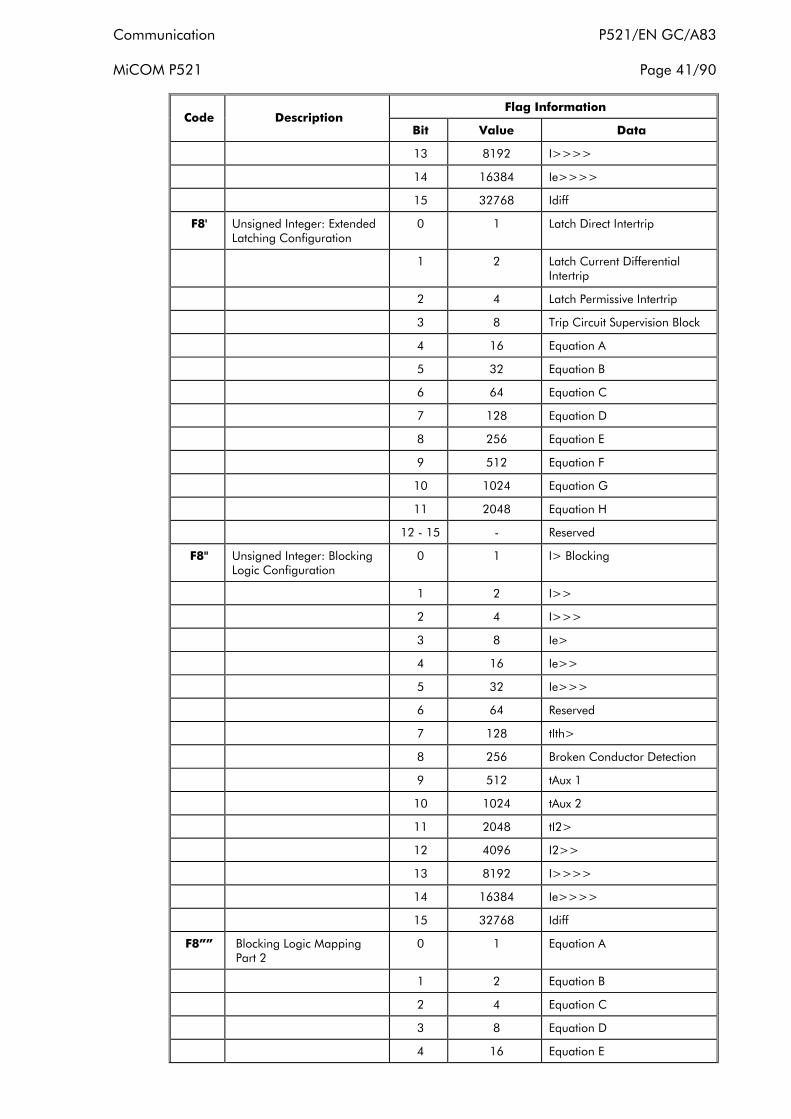
Communication P521/EN GC/A83 MiCOM P521 Page 41/90
Flag Information Code Description
Bit Value Data
13 8192 I>>>>
14 16384 Ie>>>>
15 32768 Idiff
F8' Unsigned Integer: Extended Latching Configuration
0 1 Latch Direct Intertrip
1 2 Latch Current Differential Intertrip
2 4 Latch Permissive Intertrip
3 8 Trip Circuit Supervision Block
4 16 Equation A
5 32 Equation B
6 64 Equation C
7 128 Equation D
8 256 Equation E
9 512 Equation F
10 1024 Equation G
11 2048 Equation H
12 - 15 - Reserved
F8'' Unsigned Integer: Blocking Logic Configuration
0 1 I> Blocking
1 2 I>>
2 4 I>>>
3 8 Ie>
4 16 Ie>>
5 32 Ie>>>
6 64 Reserved
7 128 tIth>
8 256 Broken Conductor Detection
9 512 tAux 1
10 1024 tAux 2
11 2048 tI2>
12 4096 I2>>
13 8192 I>>>>
14 16384 Ie>>>>
15 32768 Idiff
F8”” Blocking Logic Mapping Part 2
0 1 Equation A
1 2 Equation B
2 4 Equation C
3 8 Equation D
4 16 Equation E

P521/EN GC/A83 Communication Page 42/104 MiCOM P521
Flag Information Code Description
Bit Value Data
5 32 Equation F
6 64 Equation G
7 128 Equation H
F9 Unsigned Integer: Remote Control 1
0 1 Tripping Contact De-latched
1 2 1st Alarm Acknowledge
2 4 All Alarms Acknowledge
3 8 Remote Tripping
4 16 Remote Closing
5 32 Setting Group Change5
6 64 Thermal State Reset
7 128 Reset Max and Average Current Measurements
8 256 Disturbance Record Remote Start
9 512 Reserved
10 1024 Reserved
11 2048 Reserved
12 4096 Acknowledgement
13 8192 Oldest Event Acknowledge
14 16384 Oldest Fault Acknowledge
15 32768 Hardware SRAM Alarm Acknowledge
F10 2 Characters ASCII 32-127 ASCII Character1
32-127 ASCII Character 2
F11 Reserved
F12 Unsigned Integer: Logic Input Status
0 1 Logic Input Number 1
1 2 Logic Input Number 2
2 4 Logic Input Number 3
3 8 Logic Input Number 4
4 16 Logic Input Number 5
5 - 15 Reserved
F13 Unsigned Integer: Logic Outputs Status
0 1 Logic Output Number RL1 (Tripping)
1 2 Logic Output Number RL2
2 4 Logic Output Number RL3
3 8 Logic Output Number RL4
4 16 Logic Output Number RL0 (Watchdog)
5 Note: The Change Group Input setting must be set to EDGE.
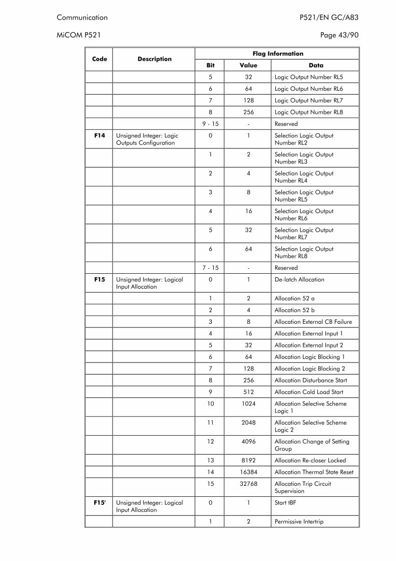
Communication P521/EN GC/A83 MiCOM P521 Page 43/90
Flag Information Code Description
Bit Value Data
5 32 Logic Output Number RL5
6 64 Logic Output Number RL6
7 128 Logic Output Number RL7
8 256 Logic Output Number RL8
9 - 15 - Reserved
F14 Unsigned Integer: Logic Outputs Configuration
0 1 Selection Logic Output Number RL2
1 2 Selection Logic Output Number RL3
2 4 Selection Logic Output Number RL4
3 8 Selection Logic Output Number RL5
4 16 Selection Logic Output Number RL6
5 32 Selection Logic Output Number RL7
6 64 Selection Logic Output Number RL8
7 - 15 - Reserved
F15 Unsigned Integer: Logical Input Allocation
0 1 De-latch Allocation
1 2 Allocation 52 a
2 4 Allocation 52 b
3 8 Allocation External CB Failure
4 16 Allocation External Input 1
5 32 Allocation External Input 2
6 64 Allocation Logic Blocking 1
7 128 Allocation Logic Blocking 2
8 256 Allocation Disturbance Start
9 512 Allocation Cold Load Start
10 1024 Allocation Selective Scheme Logic 1
11 2048 Allocation Selective Scheme Logic 2
12 4096 Allocation Change of Setting Group
13 8192 Allocation Re-closer Locked
14 16384 Allocation Thermal State Reset
15 32768 Allocation Trip Circuit Supervision
F15' Unsigned Integer: Logical Input Allocation
0 1 Start tBF
1 2 Permissive Intertrip

P521/EN GC/A83 Communication Page 44/104 MiCOM P521
Flag Information Code Description
Bit Value Data
2 4 Direct Intertrip
3 8 Communication Reset
4 16 Remote Trip via Logic Input
5 32 Remote Close via Logic Input
6 64 Trip Circuit Supervision Block
7 128 GPS Sync
8 256 LED RESET
9 512 CTS Inhibite
6 - 15 - Reserved
F16 Unsigned Integer: Threshold Earth Information Status
0 1 Overcurrent start (Ie>, Ie>>, Ie>>>, Ie>>>>)
1 2 Reserved
1 - 4 - Reserved
5 32 Start Information Ie> or Ie>> or Ie>>> or Ie>>>>
6 64 Tripping Information tIe> or tIe>> or tIe>>> or tIe>>>>
7 - 15 - Reserved
F17 Unsigned Integer: Threshold Phase Information Status
0 1 Overcurrent Start (I>, I>>, I>>>, I>>>>)
1 2 Instantaneous IA
2 4 Instantaneous IB
3 8 Instantaneous IC
4 16 Reserved
5 32 Instantaneous Information I> or I>> or I>>> or I>>>>
6 64 Tripping Information tI> or tI>> or tI>>> tI>>>>
7 - 15 - Reserved
F18 Long Integer:
- -2147483648 to
2147483647
Numerical Data
F19 Unsigned Integer: LEDs Allocation
0 1 I>
1 2 tI>
2 4 I>>
3 8 tI>>
4 16 I>>>
5 32 tI>>>
6 64 Ie>
7 128 tIe>
8 256 Ie>>

Communication P521/EN GC/A83 MiCOM P521 Page 45/90
Flag Information Code Description
Bit Value Data
9 512 tIe>>
10 1024 Ie>>>
11 2048 tIe>>>
12 4096 Thermal Overload Trip
13 8192 tI2>
14 16384 Broken Conductor Trip
15 32768 CB Failure
F19' Unsigned Integer: Extended LEDs Allocation
0 1 Logic Input 1
1 2 Logic Input 2
2 4 Logic Input 3
3 8 Logic Input 4
4 16 Logic Input 5
5 32 Reserved
6 64 Reserved
7 128 Aux 1
8 256 Aux2
9 512 t12>>
10 1024 I>>>>
11 2048 tI>>>>
12 4096 Ie>>>>
13 8192 tIe>>>>
14 - 15 Reserved
F19'' Unsigned Integer: 2nd Extension LEDs Allocation
0 - 1 Reserved
2 4 Idiff
3 8 Idiff Fail
4 16 Back-up Protection Enabled
5 32 Protection Comms Fail
6 64 Direct Intertrip
7 128 Current Differential Intertrip
8 256 Permissive Intertrip
9 512 CB Alarm
10 1024 Convention Mode
11 - 15 - Reserved
F19''' User Configurable LED Mapping (Part 4)
0 1 Equation A
1 2 Equation B
2 4 Equation C
3 8 Equation D
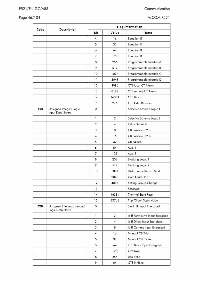
P521/EN GC/A83 Communication Page 46/104 MiCOM P521
Flag Information Code Description
Bit Value Data
4 16 Equation E
5 32 Equation F
6 64 Equation B
7 128 Equation B
8 256 Programmable Intertrip A
9 512 Programmable Intertrip B
10 1024 Programmable Intertrip C
11 2048 Programmable Intertrip D
12 4096 CTS local CT Alarm
13 8192 CTS remote CT Alarm
14 16384 CTS Block
15 32768 CTS Cdiff Restrain
F20 Unsigned Integer: Logic Input Data Status
0 1 Selective Scheme Logic 1
1 2 Selective Scheme Logic 2
2 4 Relay De-latch
3 8 CB Position (52 a)
4 16 CB Position (52 b)
5 32 CB Failure
6 64 Aux. 1
7 128 Aux. 2
8 256 Blocking Logic 1
9 512 Blocking Logic 2
10 1024 Disturbance Record Start
11 2048 Cold Load Start
12 4096 Setting Group Change
13 Reserved
14 16384 Thermal State Reset
15 32768 Trip Circuit Supervision
F20' Unsigned Integer: Extended Logic Data Status
0 1 Start tBF Input Energized
1 2 Idiff Permissive Input Energized
2 4 Idiff Direct Input Energized
3 8 Idiff Comms Input Energized
4 16 Manual CB Trip
5 32 Manual CB Close
6 64 TCS Block Input Energized
7 128 GPS Sync
8 256 LED RESET
9 64 CTS Inhibite

Communication P521/EN GC/A83 MiCOM P521 Page 47/90
Flag Information Code Description
Bit Value Data
10-15 - Reserved
F21 Unsigned Integer: Software Version
10 e.g.10 = Version 1.A
F22 Unsigned Integer: Internal Logic Data
0 1 Latching
1 - 15 - Reserved
F23 Unsigned Integer: Relay Status
0 1 Major Hardware Alarm
1 2 Minor Hardware Alarm
2 4 Presence of Non Acknowledged Event
3 8 Time Synchronization Acknowledgement
4 16 Presence of Non Acknowledged Disturbance Record
5 32 Presence of Non Acknowledged Fault Record
6 - 7 - Reserved
F24 Unsigned Integer: Relay Function Status
0 - Function disabled
1 - Function enabled
2 - 15 Reserved
F25 Phase Indication Text Selection
- 0 L1, L2, L3 and N
1 A, B, C and E
2 R, S, T and O
3 Y and B
4 W
F26 IA, IB, IC, IN Measurement Display (True RMS)
- 1 IA Measurement Display (True RMS)
- 2 IB Measurement Display (True RMS)
- 3 IC Measurement Display (True RMS)
- 4 IN Measurement Display (True RMS)
F27 Time Delay Type - 0 DMT Time Delay
- 1 IDMT Time Delay
- 2 RI Time Delay
F27' Time Delay Type - 0 DMT Time Delay
- 1 IDMT Time Delay
- 2 RI Time Delay
- 3 Belgium Curves

P521/EN GC/A83 Communication Page 48/104 MiCOM P521
Flag Information Code Description
Bit Value Data
F28 Reserved
F29 Communications Stop Bits - 0 1 Stop Bit
- 1 2 Stop Bits
F30 Communication Availability 0 Communications Non Available
1 Communications Available
F31 Unsigned Integer: Number of Available Disturbance Records
0 None
1 1 Disturbance Record Available
2 2 Disturbance Record Available
3 3 Disturbance Record Available
4 4 Disturbance Record Available
5 5 Disturbance Record Available
F32 Unsigned Integer: Disturbance Record Start Status
0 Disturbance Record Start on any Instantaneous Event.
1 Disturbance Record Start on any Trip Event
F33 Cold Load Start Thresholds 0 1 tI>
1 2 tI>>
2 4 tI>>>
3 8 tIe>
4 16 tIe>>
5 32 tIe>>>
6 64 Thermal Overload Trip
7 128 tI2>
8 256 tI2>>
9 512 tI2>>>>
10 1024 tIe>>>>
11 - 15 - Reserved
F34 Reserved
F35 Disturbance Record Uploading Status
- 0 No Disturbance Record Uploaded
- 1 Disturbance Record Upload Running
F36 Memorized Flags of Non Acknowledged Alarms:
0 1 Ie>
1 2 tIe>
2 4 Ie>>

Communication P521/EN GC/A83 MiCOM P521 Page 49/90
Flag Information Code Description
Bit Value Data
3 8 tIe>>
4 16 Ie>>>
5 32 tIe>>>
6 64 Thermal Overload Alarm
7 128 Thermal Overload Trip
8 256 Broken Conductor
9 512 CB Failure
10 1024 I2>
11 2048 I2>>
12 4096 tI2>
13 8192 tAux1
14 16384 tAux2
15 32768 tI2>>
F36' Memorized Flags of Non Acknowledged Alarms 2:
0 1 CB Open Timer Expired
1 2 CB Number of Operations
2 4 Summation Amps Exceeded Threshold
3 8 CB Supervision
4 16 CB Supervision CB Close Timer Expired
5 32 Ie>>>> Start Alarm
6 64 Ie>>>> Trip Alarm
7 - 15 - Reserved
F37 Unsigned Integer: Thermal Overload Information
0 1 Thermal Overload Alarm
1 2 Thermal Overload Trip
2 - 15 - Reserved
F38 Unsigned Integer: CB Alarm/CB Failure/Broken Conductor Flags
0 1 Reserved
1 2 CB Failure
2 4 Pole A Opening
3 8 Pole B Opening
4 16 Pole C Opening
5 32 Broken Conductor
6 64 tAux1
7 128 tAux2
8 256 Broken Conductor Time Delay
9 512 CB Failure Time Delay
10 1024 Cold Load Pickup Time Delay
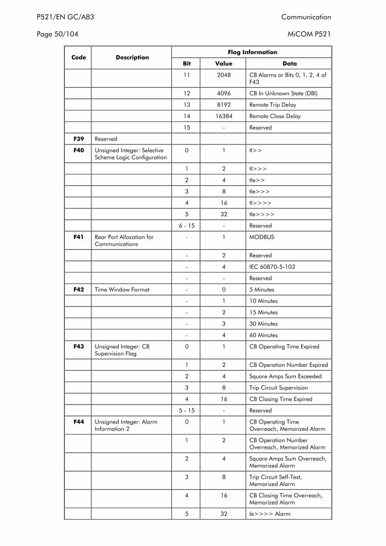
P521/EN GC/A83 Communication Page 50/104 MiCOM P521
Flag Information Code Description
Bit Value Data
11 2048 CB Alarms or Bits 0, 1, 2, 4 of F43
12 4096 CB In Unknown State (DBI)
13 8192 Remote Trip Delay
14 16384 Remote Close Delay
15 - Reserved
F39 Reserved
F40 Unsigned Integer: Selective Scheme Logic Configuration
0 1 tI>>
1 2 tI>>>
2 4 tIe>>
3 8 tIe>>>
4 16 tI>>>>
5 32 tIe>>>>
6 - 15 - Reserved
F41 Rear Port Allocation for Communications
- 1 MODBUS
- 2 Reserved
- 4 IEC 60870-5-103
- - Reserved
F42 Time Window Format - 0 5 Minutes
- 1 10 Minutes
- 2 15 Minutes
- 3 30 Minutes
- 4 60 Minutes
F43 Unsigned Integer: CB Supervision Flag
0 1 CB Operating Time Expired
1 2 CB Operation Number Expired
2 4 Square Amps Sum Exceeded
3 8 Trip Circuit Supervision
4 16 CB Closing Time Expired
5 - 15 - Reserved
F44 Unsigned Integer: Alarm Information 2
0 1 CB Operating Time Overreach, Memorized Alarm
1 2 CB Operation Number Overreach, Memorized Alarm
2 4 Square Amps Sum Overreach, Memorized Alarm
3 8 Trip Circuit Self-Test, Memorized Alarm
4 16 CB Closing Time Overreach, Memorized Alarm
5 32 Ie>>>> Alarm

Communication P521/EN GC/A83 MiCOM P521 Page 51/90
Flag Information Code Description
Bit Value Data
6 64 tIe>>>> Alarm
7 128 TCS Block
8-15 - Reserved
F45 Unsigned Integer: Relay Status
0 1 Watchdog
1 2 Communication Failure
2 4 EEPROM Data Failure
3 8 CT Failure
4 16 Real Time Clock Failure
5 32 EEPROM Calibration Failure
6 64 SRAM Failure
7 128 Reserved
8 256 Comms FPGA Total Failure
9 512 Reprogramming Comms FPGA in Progress
10 1024 Factory Default Settings Restored
11 - 15 - Reserved
F46 Unsigned Integer: Remote Control Word 3
0 1 Initiate Ie Harmonic Calculation
1 2 De-latch Trip Relay Only (RL1)
2 4 Acknowledge Oldest Disturbance Record
3 8 Reserved
4 16 Reset Rolling Demand Measurements
5 32 Reset Peak Average Measurements
6 64 Clear the Protection Communication Statistics
7 128 Cancel Remote Trip Sequence
8 256 Cancel Remote Close Sequence
9 512 Reserved
10 1024 Reserved
11 2048 Reserved
12 4096 Reserved
13 8192 Reserved
14 16384 Erase all records (events, faults, alarms, disturbances, etc)
15 32768 Reserved
F47 Change Group Input 0 Edge triggered changes of logic inputs
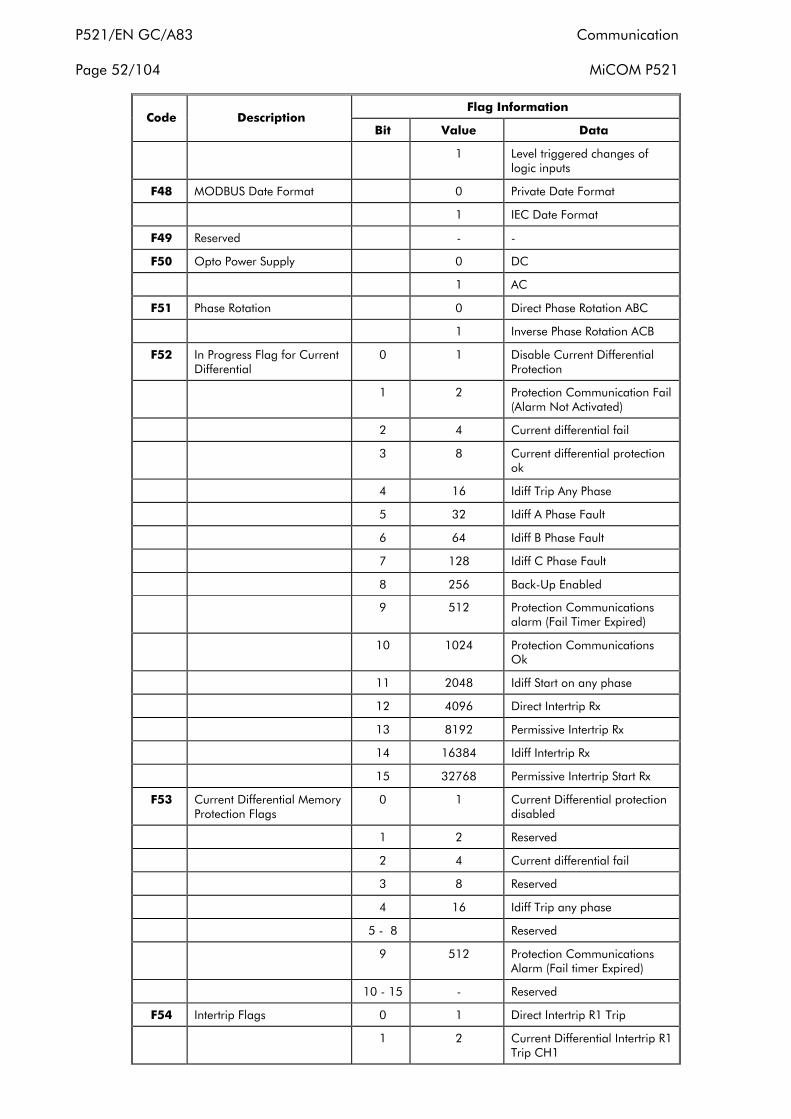
P521/EN GC/A83 Communication Page 52/104 MiCOM P521
Flag Information Code Description
Bit Value Data
1 Level triggered changes of logic inputs
F48 MODBUS Date Format 0 Private Date Format
1 IEC Date Format
F49 Reserved - -
F50 Opto Power Supply 0 DC
1 AC
F51 Phase Rotation 0 Direct Phase Rotation ABC
1 Inverse Phase Rotation ACB
F52 In Progress Flag for Current Differential
0 1 Disable Current Differential Protection
1 2 Protection Communication Fail (Alarm Not Activated)
2 4 Current differential fail
3 8 Current differential protection ok
4 16 Idiff Trip Any Phase
5 32 Idiff A Phase Fault
6 64 Idiff B Phase Fault
7 128 Idiff C Phase Fault
8 256 Back-Up Enabled
9 512 Protection Communications alarm (Fail Timer Expired)
10 1024 Protection Communications Ok
11 2048 Idiff Start on any phase
12 4096 Direct Intertrip Rx
13 8192 Permissive Intertrip Rx
14 16384 Idiff Intertrip Rx
15 32768 Permissive Intertrip Start Rx
F53 Current Differential Memory Protection Flags
0 1 Current Differential protection disabled
1 2 Reserved
2 4 Current differential fail
3 8 Reserved
4 16 Idiff Trip any phase
5 - 8 Reserved
9 512 Protection Communications Alarm (Fail timer Expired)
10 - 15 - Reserved
F54 Intertrip Flags 0 1 Direct Intertrip R1 Trip
1 2 Current Differential Intertrip R1 Trip CH1

Communication P521/EN GC/A83 MiCOM P521 Page 53/90
Flag Information Code Description
Bit Value Data
2 4 Permissive Intertrip Start CH1
3 8 Permissive Intertrip Trip CH1
4-15 - Reserved
F55 Reserved
F56 Commissioning Flags 0 Output Contacts Disabled
1 Protection Communications Loopback Mode Enabled
2 Reserved
F57 Unsigned Long Integer 4294967295 Numerical Data
F58 Protection Communication Protocol
0 SDLC
1 NRZ
2 Inverted NRZ
F59 Protection Communication Data Rate
0 64 kbits/Sec
1 56 kbits/Sec
2 19.2 kbits/Sec
3 9.6 kbits/Sec
F60 Protection Communication Relay Address
0 1A
1 1B
2 2A
3 2B
4 3A
5 3B
6 4A
7 4B
8 5A
9 5B
10 6A
11 6B
12 7A
13 7B
14 8A
15 8B
16 9A
17 9B
18 10A

P521/EN GC/A83 Communication Page 54/104 MiCOM P521
Flag Information Code Description
Bit Value Data
19 10B
20 11A
21 11B
22 12A
23 12B
24 13A
25 13B
26 14A
27 14B
28 15A
29 15B
30 16A
31 16B
F61 Protection Communication Clock Source
0 Internal
1 External
F62 Unsigned Integer : Logic Outputs Configuration
0 Selection Logic Output Number RL1
1 Selection Logic Output Number RL2
2 Selection Logic Output Number RL3
3 Selection Logic Output Number RL4
4 Selection Logic Output Number RL5
5 Selection Logic Output Number RL6
6 Selection Logic Output Number RL7
7 Selection Logic Output Number RL8
F63 Unsigned Integer: Manual CB Trip and Close
0 No Operation
1 Trip
2 Close
F64 Latest Fault Record Register 0 1 I2> Fault
1 2 I2>> Fault
2 4 Thermal Fault
3 8 Aux. 1
4 16 Aux. 2
5 32 I<
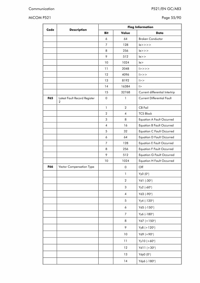
Communication P521/EN GC/A83 MiCOM P521 Page 55/90
Flag Information Code Description
Bit Value Data
6 64 Broken Conductor
7 128 Ie>>>>
8 256 Ie>>>
9 512 Ie>>
10 1024 Ie>
11 2048 I>>>>
12 4096 I>>>
13 8192 I>>
14 16384 I>
15 32768 Current differential Intertrip
F65 Latest Fault Record Register 2
0 1 Current Differential Fault
1 2 CB Fail
2 4 TCS Block
3 8 Equation A Fault Occurred
4 16 Equation B Fault Occurred
5 32 Equation C Fault Occurred
6 64 Equation D Fault Occurred
7 128 Equation E Fault Occurred
8 256 Equation F Fault Occurred
9 512 Equation G Fault Occurred
10 1024 Equation H Fault Occurred
F66 Vector Compensation Type 0 Off
1 Yy0 (0°)
2 Yd1 (-30°)
3 Yy2 (-60°)
4 Yd3 (-90°)
5 Yy4 (-120°)
6 Yd5 (-150°)
7 Yy6 (-180°)
8 Yd7 (+150°)
9 Yy8 (+120°)
10 Yd9 (+90°)
11 Yy10 (+60°)
12 Yd11 (+30°)
13 Ydy0 (0°)
14 Ydy6 (-180°)

P521/EN GC/A83 Communication Page 56/104 MiCOM P521
Flag Information Code Description
Bit Value Data
F67 Selective Intertripping 0 1 DIT on tI> Trip
1 2 DIT on tI>> Trip
2 4 DIT on tI>>> Trip
3 8 DIT on tI>>>> Trip
4 16 DIT on tIe> Trip
5 32 DIT on tIe>> Trip
6 64 DIT on tIe>>> Trip
7 128 DIT on tIe>>>> Trip
8 256 DIT on tI< Trip
9 512 DIT on tI2> Trip
10 1024 DIT on tI2>> Trip
11 2048 DIT on Thermal Trip
12 4096 DIT on Broken Conductor Trip
13 8192 DIT on tAux1 Trip
14 16384 DIT on tAux2 Trip
15 32768 DIT on CB Fail
F68 PIT I Selection 0 1 Remote
1 2 Local
F69 PIT OC Stages 0 1 I>
1 2 I>>
2 4 I>>>
3 8 I>>>>
4 16 Ie>
4 32 Ie>>
5 64 Ie>>>
7 128 Ie>>>>
F70 Inrush Block Control Flags 0 1 Local Cross Block
1 2 Local Phase A Block
2 4 Local Phase B Block
3 8 Local Phase C Block
4 16 Remote Cross Block
5 32 Remote Phase A Block
6 64 Remote Phase B Block
7 128 Remote Phase C Block
8 256 Remote Inrush Block Enabled
9 512 Inrush Block Configure Error

Communication P521/EN GC/A83 MiCOM P521 Page 57/90
Flag Information Code Description
Bit Value Data
F71 Inrush Block Control alarms 0 1 Inrush Block Configure Error Alarm
F72 CTS Control Flags 0 1 Local CTS Fail
1 2 Remote CTS Fail
2 4 CTS Block
3 8 CTS Cdiff Block
4 16 CTS Cdiff Restrain
5 32 CTS Inhibited
6 64 CTS Conf Fail
F73 CTS Control Alarms 0 1 Local CTS Fail Alarm
1 2 Remote CTS Fail Alarm
2 4 CTS Block Alarm
3 8 Reserved
4 16 CTS Cdiff Restrain Alarm
5 32 CTS Inhibited Alarm
6 64 CTS Conf Fail Alarm
F74 CTS reset mode 0 Manual
1 Auto
F75 Loopback mode 0 Off
1 Channel 1
2 Internal
F76 Reserved
F77 Reserved
F78 Reserved
F79 Reserved
F80 FRAME mode 0 Extension
1 Convention
F81 Logic Equation Flag 0 1 Equation A
1 2 Equation B
2 4 Equation C
3 8 Equation D
4 16 Equation E
5 32 Equation F
6 64 Equation G
7 128 Equation H
F82 Programmable Intertrip 0 1 Intertrip 1
1 2 Intertrip 2
2 4 Intertrip 3
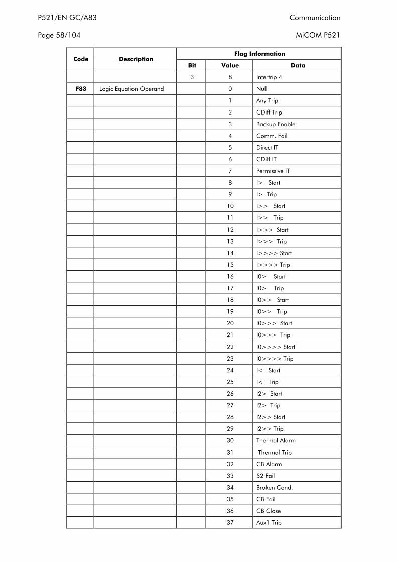
P521/EN GC/A83 Communication Page 58/104 MiCOM P521
Flag Information Code Description
Bit Value Data
3 8 Intertrip 4
F83 Logic Equation Operand 0 Null
1 Any Trip
2 CDiff Trip
3 Backup Enable
4 Comm. Fail
5 Direct IT
6 CDiff IT
7 Permissive IT
8 I> Start
9 I> Trip
10 I>> Start
11 I>> Trip
12 I>>> Start
13 I>>> Trip
14 I>>>> Start
15 I>>>> Trip
16 I0> Start
17 I0> Trip
18 I0>> Start
19 I0>> Trip
20 I0>>> Start
21 I0>>> Trip
22 I0>>>> Start
23 I0>>>> Trip
24 I< Start
25 I< Trip
26 I2> Start
27 I2> Trip
28 I2>> Start
29 I2>> Trip
30 Thermal Alarm
31 Thermal Trip
32 CB Alarm
33 52 Fail
34 Broken Cond.
35 CB Fail
36 CB Close
37 Aux1 Trip

Communication P521/EN GC/A83 MiCOM P521 Page 59/90
Flag Information Code Description
Bit Value Data
38 Aux2 Trip
39 Active Group
40 TCS Block
41 Input 1
42 Input 2
43 Input 3
44 Input 4
45 Input 5
46 Equ A
47 Equ B
48 Equ C
49 Equ D
50 Equ E
51 Equ F
52 Equ G
53 Equ H
54 Prgm IT 1
55 Prgm IT 2
56 Prgm IT 3
57 Prgm IT 4
58 CTS Local Alarm
59 CTS Remote Alarm
60 CTS Block
61 CTS Restrain
62 Convention Mode
63 Cdiff Disabled
F84 Logic Equation Operator 0 OR
1 OR NOT
2 AND
3 AND NOT
F85 Programmable Intertrip Allocation 0 0 I> Trip
1 2 I>> Trip
2 4 I>>> Trip
3 8 I>>>> Trip
4 16 I0> Trip
5 32 I0>> Trip
6 64 I0>>> Trip
7 128 I0>>>> Trip
8 256 Thermal Trip

P521/EN GC/A83 Communication Page 60/104 MiCOM P521
Flag Information Code Description
Bit Value Data
9 512 I< Trip
10 1024 I2> Trip
11 2048 I2>> Trip
12 4096 CB Fail
13 8192 Broken Cond.
14 16384 Aux1 Trip
15 32768 Aux2 Trip
F85’ Porgrammable Intertrip Allocation Word 2 0 1 Input 1
1 2 Input 2
2 4 Input 3
3 8 Input 4
4 16 Input 5
5 32 Equ A
6 64 Equ B
7 128 Equ C
8 256 Equ D
9 512 Equ E
10 1024 Equ F
11 2048 Equ G
12 4096 Equ H
F86 message display
F87 FRAME mode 0 1 Convention
1 2 Reserved
2 4 Conf conflict comms
3.5 Event record
There are two methods of event record extraction.
1. Request a specific event record (Ref. section 3.5.1)
2. Request the oldest non-acknowledged event record (Ref. section 3.5.2)
3.5.1 Specific event record extraction
3.5.1.1 Page 35h: contains 75 event records from 3500h to 354Ah
One event record can be accessed from each address.
Each event is one 3 dimensional MODBUS register (see ref. [3.2]) that consists of 9 data words. The format is detailed in 3.5.1.2 below.

Communication P521/EN GC/A83 MiCOM P521 Page 61/90
3.5.1.2 Event record format
Word N° 1: Event meaning see ref. 3.5.1.3
Word N° 2: MODBUS associated value
Word N° 3: MODBUS address
Word N° 4: Reserved
Word N° 5 & 6: Event date (second) number of second since 01/01/94
Word N° 7 & 8: Event date (millisecond)
Word N° 9: Acknowledge
0 = Event Non acknowledged
1 = Event Acknowledged
3.5.1.3 Event table
Code Event Meaning Type MODBUS Address
0 No Event -
1 Remote Closing F9 014H
2 Remote Tripping F9 014H
3 Disturbance Recording Start F9
4 Trip Output De-latch F46 014H
5 Setting Change ADDRESS
6 Remote Thermal Reset F46
7 NULL -
8 NULL -
9 I> F17↑↓ 016H
10 I>> F17↑↓ 017H
11 I>>> F17↑↓ 018H
12 I>>>> F17↑↓ 019H
13 Ie> F16↑↓ 01AH
14 Ie>> F16↑↓ 01BH
15 Ie>>> F16↑↓ 01CH
16 Ie>>>> F16↑↓ 01DH
17 Thermal Overload Alarm F37↑↓ 02AH
18 Thermal Overload Threshold F37↑↓ 02AH
19 tI> F17↑↓ 016H
20 tI>> F17↑↓ 017H
21 tI>>> F17↑↓ 018H

P521/EN GC/A83 Communication Page 62/104 MiCOM P521
Code Event Meaning Type MODBUS Address
22 tI>>>> F17↑↓ 019H
23 tIe> F16↑↓ 01AH
24 tIe>> F16↑↓ 01BH
25 tIe>>> F16↑↓ 01CH
26 tIe>>>> F16↑↓ 01DH
27 tI< F16↑↓ 02AH
28 Broken Conductor F38↑↓ 02DH
29 t Aux 1 F38↑↓ 02DH
30 t Aux 2 F38↑↓ 02DH
31 CB Failure F38↑↓ 033H
32 Selective Scheme Logic 1 F20↑↓ 011H
33 Selective Scheme Logic 2 F20↑↓ 011H
34 Blocking Logic 1 F20↑↓ 011H
35 Blocking Logic 2 F20↑↓ 011H
36 Setting Group Change F20↑↓ 011H
37 52a F20↑↓ 011H
38 52b F20↑↓ 011H
39 Acknowledgement of the Output Relay Latched by Logic Input F20↑↓ 011H
40 NULL -
41 Cold Load Start F20↑↓ 011H
42 NULL -
43 NULL -
44 NULL -
45 Input Logic State Change F12↑↓ 010H
46 NULL -
47 NULL -
48 NULL -
49 NULL -
50 NULL -
51 NULL -
52 NULL -
53 NULL -
54 NULL -

Communication P521/EN GC/A83 MiCOM P521 Page 63/90
Code Event Meaning Type MODBUS Address
55 NULL -
56 NULL -
57 NULL -
58 NULL -
59 Output Relays Command F39↑↓ 014H
60 Front Panel Single Alarm Acknowledgement -
61 Front Panel All Alarms Acknowledgement -
62 Remote Single Alarm Acknowledgement -
63 Remote All Alarms Acknowledgement -
64 Major Hardware Alarms F45↑↓ 00FH
65 Minor Hardware Alarms F45↑↓ 00FH
66 I2> F16↑↓ 02BH
67 tI2> F16↑↓ 02BH
68 CB Supervision CB Open Timer Expired Event F43↑↓ 033H
69 CB Supervision Number of Operations Expired Event F43↑↓ 033H
70 Summation Amps Exceeded Threshold Event F43↑↓ 033H
71 Trip Circuit Supervision F43↑↓ 033H
72 CB Supervision CB Closed Timer Expired Flag F43↑↓ 033H
73 CB Status is Indeterminate F38↑↓ 033H
74 NULL -
75 NULL -
76 NULL -
77 NULL -
78 NULL -
79 NULL -
80 NULL -
81 Relay Update Event F13↑↓ 033H
82 Start tBF Input Energized Event F20'↑↓ 012H
83 I< F16↑↓ 02BH
84 I2>> F16↑↓ 02BH
85 tI2>> F16↑↓ 02BH
86 NULL -
87 NULL -
88 Protection Comms Alarms Channel 1 F52↑ 015H

P521/EN GC/A83 Communication Page 64/104 MiCOM P521
Code Event Meaning Type MODBUS Address
89 NULL -
90 Differential Protection Trip F52↑↓ 015H
91 Direct Intertrip Channel 1 F52↑ 015H
92 Current Differential Intertrip Channel 1 F52↑ 015H
93 Permissive Intertrip Channel 1 F52↑ 015H
94 NULL -
95 NULL -
96 NULL -
97 Differential Protection Fail F52↑ 015H
98 Cdiff Protection Disabled F52↑↓ 015H
99 Protection Communications Loopback F56↑↓ 036H
100 Output Contacts Disabled F24↑↓ 036H
101 Differential Protection Start F52↑↓ 015H
102 NULL -
103 NULL -
104 NULL -
105 NULL -
106 NULL -
107 NULL -
108 Protection Comms Fail F52↑↓ 015H
109 Differential Communications Channel 1 OK F52↑↓ 015H
110 NULL -
111 Backup Protection Active F52↑↓ 015H
112 Differential Protection OK F52↑ 015H
113 Permissive Intertrip Start Channel 1 F52↑↓ 015H
114 NULL -
115 NULL -
116 NULL -
117 NULL -
118 NULL -
119 Manual Trip Delay Timer Start F38↑↓ 02DH
120 Manual Close Delay Timer Start F38↑↓ 02DH
121 Communication Statistics reset
122 TCS Block Input Energized F20’↑↓ 012H
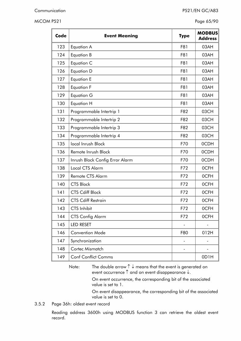
Communication P521/EN GC/A83 MiCOM P521 Page 65/90
Code Event Meaning Type MODBUS Address
123 Equation A F81 03AH
124 Equation B F81 03AH
125 Equation C F81 03AH
126 Equation D F81 03AH
127 Equation E F81 03AH
128 Equation F F81 03AH
129 Equation G F81 03AH
130 Equation H F81 03AH
131 Programmable Intertrip 1 F82 03CH
132 Programmable Intertrip 2 F82 03CH
133 Programmable Intertrip 3 F82 03CH
134 Programmable Intertrip 4 F82 03CH
135 local Inrush Block F70 0CDH
136 Remote Inrush Block F70 0CDH
137 Inrush Block Config Error Alarm F70 0CDH
138 Local CTS Alarm F72 0CFH
139 Remote CTS Alarm F72 0CFH
140 CTS Block F72 0CFH
141 CTS Cdiff Block F72 0CFH
142 CTS Cdiff Restrain F72 0CFH
143 CTS Inhibit F72 0CFH
144 CTS Config Alarm F72 0CFH
145 LED RESET - -
146 Convention Mode F80 012H
147 Synchronization - -
148 Cortec Mismatch - -
149 Conf Conflict Comms 0D1H
Note: The double arrow ↑ ↓ means that the event is generated on event occurrence ↑ and on event disappearance ↓.
On event occurrence, the corresponding bit of the associated value is set to 1.
On event disappearance, the corresponding bit of the associated value is set to 0.
3.5.2 Page 36h: oldest event record
Reading address 3600h using MODBUS function 3 can retrieve the oldest event record.

P521/EN GC/A83 Communication Page 66/104 MiCOM P521
3.5.3 Event acknowledgement
There are two ways to acknowledge an event, automatically or manually.
3.5.3.1 Event acknowledgement mode
In order to set the acknowledgement mode for events and faults, bit 12 in remote control word 1 (0400h) has to be written to with the required mode see ref. [3.5.3.4 Event acknowledgement control]
3.5.3.2 Automatic event acknowledgement mode
Acknowledgement of the oldest non-acknowledged event record takes place on retrieval.
3.5.3.3 Manual event acknowledgement
With the acknowledgement mode set to manual, the oldest non-acknowledged event record must be retrieved. Bit 13 of remote control word 1 (0400h) can then be set to 1 to acknowledge the oldest non-acknowledged event ref. [3.5.3.4 Event acknowledgement control].
3.5.3.4 Event acknowledgement control
Remote Control Word 1 : 0400h
Function
Bit 12 0 = Automatic event/fault acknowledgement mode
1 = Manual event/fault acknowledgement mode
Bit 13 0 = Event not acknowledged manually
1 = Event acknowledged manually
3.6 Fault record
There are two methods of fault record extraction.
1. Request a specific fault record (ref. section 3.6.1)
2. Request the oldest non-acknowledged fault record (ref. section 3.6.2).
3.6.1 Specific fault record
3.6.1.1 Page 37h: fault record mapping
Each fault record is one 3 dimensional MODBUS register (see ref. [3.2]) that consists of 25 data words. The format is detailed in 3.6.1.2 below.
Address Contents
3700h Fault Record N° 1
3701h Fault Record N° 2
3702h Fault Record N° 3
3703h Fault Record N° 4
3704h Fault Record N° 5
3705h Fault Record N° 6

Communication P521/EN GC/A83 MiCOM P521 Page 67/90
Address Contents
3706h Fault Record N° 7
3707h Fault Record N° 8
3708h Fault Record N° 9
3709h Fault Record N° 10
370Ah Fault Record N° 11
370Bh Fault Record N° 12
370Ch Fault Record N° 13
370Dh Fault Record N° 14
370Eh Fault Record N° 15
370Fh Fault Record N° 16
3710h Fault Record N° 17
3711h Fault Record N° 18
3712h Fault Record N° 19
3713h Fault Record N° 20
3714h Fault Record N° 21
3715h Fault Record N° 22
3716h Fault Record N° 23
3717h Fault Record N° 24
3718h Fault Record N° 25
3E00h Oldest Non-Acknowledged Fault Record
3.6.1.2 Fault record format
Word Number Contents
1 Fault number
2 & 3 Fault time in seconds since 01/01/94
4 & 5 Fault time (milliseconds)
6 Fault date (season) 0 = winter 1= Summer 2 = Undefined
7 Active setting group
8 Fault type (see table 1)
9 Fault element (see table 2)
10 & 11 Fault value current (see note 1)
12 Phase A current (see note 2)
13 Phase B current (see note 2)
14 Phase C current (see note 2)
15 Earth current value (see note 2)

P521/EN GC/A83 Communication Page 68/104 MiCOM P521
Word Number Contents
16 & 17 IA differential current (see note 3)
18 & 19 IB differential current (see note 3)
20 & 21 IC differential current (see note 3)
22 & 23 Ibias highest current (see note 3)
24 Cdiff control flags (see F52)
25 Acknowledge fault : Fault non acknowledged = 0 Fault acknowledged = 1
Table 1: table of fault types
0 None
1 Phase A
2 Phase B
3 Phase C
4 Phases A - B
5 Phases A - C
6 Phases B - C
7 Phases A – B - C
8 Earth
Table 2: table of fault element meanings
Code Fault Origin
00 Null event
01 Remote trip
02 Thermal overload trip
03 tI> trip
04 tI>> trip
05 tI>>> trip
06 tI>>>> trip
07 tIe> trip
08 tIe>> trip
09 tIe>>> trip
10 tIe>>>> trip
11 tI < trip
12 Broken conductor trip
13 t Aux 1 trip
14 t Aux 2 trip
15 tI2> trip

Communication P521/EN GC/A83 MiCOM P521 Page 69/90
Code Fault Origin
16 tI2>> trip
17 Idiff trip
18 Intertrip
19 TCS Block
20 EQU A Trip
21 EQU B Trip
22 EQU C Trip
23 EQU D Trip
24 EQU E Trip
25 EQU F Trip
26 EQU G Trip
27 EQU H Trip
Note 1: For trip codes 17 & 18 (in table 2) refer to note 3 to calculate the value. For all other trip codes refer to note 2 to calculate the value.
Note 2: The nominal current value not including any CT ratio settings.
3.6.1.3 Fault record calculation formulae
Line Current Differential/Bias Value =
Differential or Bias Current (word 16 & 17 or 18 & 19 or 20 & 21 or 22 & 23)
100
Line Phase Current Value =
Phase Sampled Value (word 11, 12, 13 or 14) *Phase Primary CT Ratio (0120h)
Phase Internal CT Ratio (0007h)
Line Earth Current Value =
Earth Sampled Value (word 10 or 15) *Earth Primary CT Ratio (0122h)
Earth Internal CT Ratio (0008h)
The earth internal CT ratio is dependent on the earth current range as shown in the table below:
3.6.1.4 Internal CT value for each sensitivity range
Sensitivity Range 0.1 to 40 Ιen 0.01 to 8 Ιen 0.002 to 1 Ιen
Internal CT Value 800 3277 32700
Note 3: Current differential value calculation.
Line Current Differential/Bias Value =
Differential or Bias Current (word 16 & 17 or 18 & 19 or 20 & 21 or 22 & 23)
100

P521/EN GC/A83 Communication Page 70/104 MiCOM P521
3.6.2 Oldest non acknowledged fault record
3.6.2.1 Page 3Eh: oldest non acknowledged fault record
Reading address 3E00h using MODBUS function 3 can retrieve the oldest non-acknowledged fault record.
3.6.3 Fault record acknowledgement
3.6.4 Event acknowledgement
There are two ways to acknowledge an event, automatically or manually.
3.6.4.1 Event acknowledgement mode
In order to set the acknowledgement mode for events and faults, bit 12 in remote control word 1 (0400h) has to be written to with the required mode see ref. [3.5.3.4 Event acknowledgement control]
3.6.4.2 Automatic event acknowledgement mode
Acknowledgement of the oldest non acknowledged event record takes place on retrieval.
3.6.4.3 Manual event acknowledgement
With the acknowledgement mode set to manual, the oldest non-acknowledged event record must be retrieved. Bit 14 of remote control word 1 (0400h) can then be set to 1 to acknowledge the oldest non-acknowledged event ref. [3.5.3.4 Event acknowledgement control].
Remote Control Word 1 : 0400h
Function
Bit 12 0 = Automatic event/fault acknowledgement mode
1 = Manual event/fault acknowledgement mode
Bit 14 0 = Fault record not acknowledged manually
1 = Fault record acknowledged manually
3.7 Disturbance records
In order to extract a disturbance record the following requests need to be sent to the relay.
1. An optional request can be sent to extract a summary of all the disturbance records in SRAM, the mapping and format of the data returned is shown in section 3.6.1.
2. Read the configuration information for the first set of channel data. The first set is IA. The MODBUS mapping and format are detailed in section 3.7.2. Reading the channel configuration data is required to selects which channel data is available for reading.
3. Read the first 250 words of the selected channel data. The MODBUS mapping and format is detailed in section 3.7.3 Channel data.
4. Continue to request configuration information and then channel data in 250 word blocks until all the disturbance record has been extracted. Data words 10 and 11 of the configuration information specify the end of the channel extraction.

Communication P521/EN GC/A83 MiCOM P521 Page 71/90
5. Read the upload index frame to complete the disturbance record extraction and to acknowledge the disturbance record extraction. Refer to section 3.7.3 for the format and MODBUS mapping details.
3.7.1 Summary disturbance records
3.7.1.1 Page 3Dh: summary disturbance records
The summary disturbance record is one 3 dimensional MODBUS register (see ref. [3.2]) that consists of 36 data words. The format is detailed in 3.7.1.2 below.
MODBUS function 3 can be used to read the 5 summary disturbance records.
3.7.1.2 Format of summary disturbance records
Word Number Contents
1 Number of disturbance records available
2 Oldest disturbance record number
3 & 4 Oldest disturbance record time (seconds)
5 & 6 Oldest disturbance record time (milliseconds)
7 Disturbance record starting origin
1 = Trip relay (RL1), 2 = Instantaneous threshold, 3 = Remote command, 4 = Logic input
8 Acknowledge
9 Oldest disturbance record number +1
10 & 11 Disturbance record time (seconds)
12 & 13 Disturbance record time (milliseconds)
14 Disturbance record starting origin
1 = Trip relay (RL1), 2 = Instantaneous threshold, 3 = Remote command, 4 = Logic input
15 Acknowledge
16 Oldest disturbance record number +2
17 & 18 Disturbance record time (seconds)
19 & 20 Disturbance record time (milliseconds)
21 Disturbance record starting origin
1 = Trip relay (RL1), 2 = Instantaneous threshold, 3 = Remote command, 4 = Logic input
22 Acknowledge
23 Oldest disturbance record number +3
24 & 25 Disturbance record time (seconds)
26 & 27 Disturbance record time (milliseconds)
28 Disturbance record starting origin
1 = Trip relay (RL1) , 2 = Instantaneous threshold, 3 = Remote command, 4 = Logic input

P521/EN GC/A83 Communication Page 72/104 MiCOM P521
Word Number Contents
29 Acknowledge
30 Latest disturbance record
31 & 32 Latest disturbance record time (seconds)
33 & 34 Latest disturbance record time (milliseconds)
35 Disturbance record starting origin
1 = Trip relay (RL1), 2 = Instantaneous threshold, 3 = Remote command, 4 = Logic input
36 Acknowledge
3.7.2 Channel selection and configuration
3.7.2.1 Pages 38h to 3Ch: data mapping
All channel selection and configuration registers are 3 dimensional MODBUS registers (see ref. [3.2]) which consist of 11 data words. The format is detailed in 3.7.2.2 below.
MODBUS function 3 can be used to read the summary disturbance records.
Address Disturbance Record No. Format
3800h 1 IA
3801h 1 IB
3802h 1 IC
3803h 1 IE
3804h 1 Timing
3805h 1 Logic input and output 1
3806h 1 Logic input and output 2
3900h 2 IA
3901h 2 IB
3902h 2 IC
3903h 2 IE
3904h 2 Timing
3905h 2 Logic input and output 1
3906h 2 Logic input and output 2
3A00h 3 IA
3A01h 3 IB
3A02h 3 IC
3A03h 3 IE
3A04h 3 Timing
3A05h 3 Logic input and output 1

Communication P521/EN GC/A83 MiCOM P521 Page 73/90
Address Disturbance Record No. Format
3A06h 3 Logic input and output 2
3B00h 4 IA
3B01h 4 IB
3B02h 4 IC
3B03h 4 IE
3B04h 4 Timing
3B05h 4 Logic input and output 1
3B06h 4 Logic input and output 2
3C00h 5 IA
3C01h 5 IB
3C02h 5 IC
3C03h 5 IE
3C04h 5 Timing
3C05h 5 Logic input and output 1
3C06h 5 Logic input and output 2
3.7.2.2 Disturbance record channel selection and configuration format
Word Number
Format
Word No 1 Number of samples to be extracted
Word No 2 Number of samples in pre-time
Word No 3 Number of samples in post-time
Word No 4 Primary phase CT ratio
Word No 5 Secondary phase CT ratio
Word No 6 Primary earth CT ratio
Word No 7 Secondary earth CT ratio
Word No 8 Internal phase CT ratio
Word No 9 Internal earth CT ratio
Word No 10 Address of the last page of disturbance record data
Word No 11 Number of data words on the last page of the disturbance record for this channel

P521/EN GC/A83 Communication Page 74/104 MiCOM P521
3.7.3 Channel data
3.7.3.1 Page 9h to 21h: channel data mapping
Addresses Contents
0900H to 09FAH 250 Disturbance data words
0A00H to 0AFAH 250 Disturbance data words
0B00H to 0BFAH 250 Disturbance data words
0C00H to 0CFAH 250 Disturbance data words
0D00H to 0DFAH 250 Disturbance data words
0E00H to 0EFAH 250 Disturbance data words
0F00H to 0FFAH 250 Disturbance data words
1000H to 10FAH 250 Disturbance data words
1100H to 11FAH 250 Disturbance data words
1200H to 12FAH 250 Disturbance data words
1300H to 13FAH 250 Disturbance data words
1400H to 14FAH 250 Disturbance data words
1500H to 15FAH 250 Disturbance data words
1600H to 16FAFH 250 Disturbance data words
1700H to 17AFH 250 Disturbance data words
1800H to 18AFH 250 Disturbance data words
1900H to 19AFH 250 Disturbance data words
1A00H to 1AAFH 250 Disturbance data words
1B00H to 1BAFH 250 Disturbance data words
1C00H to 1CAFH 250 Disturbance data words
1D00H to 1DAFH 250 Disturbance data words
1E00H to 1EAFH 250 Disturbance data words
1F00H to 1FAFH 250 Disturbance data words
2000H to 20FAH 250 Disturbance data words
2100H to 21FAH 250 Disturbance data words
3.7.3.2 Format of the disturbance record channel data
Channel Name Format
IA 16 bit word equivalent to the ADC count (Ref. Note 1)
IB 16 bit word equivalent to the ADC count (Ref. Note 1)
IC 16 bit word equivalent to the ADC count (Ref. Note 1)
IE 16 bit word equivalent to the ADC count (Ref. Note 2)
Timing Time between two samples in microseconds

Communication P521/EN GC/A83 MiCOM P521 Page 75/90
Channel Name Format
Logic channel 1 16 bit word (see table 1 for format)
Logic channel 2 16 bit word (see table 2 for format)
3.7.3.3 Calculation formulae
Line Phase Current Value =
Phase Sampled Value (word 11, 12, 13 or 14) *Phase Primary CT Ratio (0120h)
Phase Internal CT Ratio (0007h)
Line Earth Current Value =
Earth Sampled Value (word 10 or 15) *Earth Primary CT Ratio (0122h)
Earth Internal CT Ratio (0008h)
The earth internal CT ratio is dependent on the earth current range as shown in the table below:
Sensitivity range 0.1 to 40 Ιen 0.01 to 8 Ιen 0.002 to 1 Ιen
Internal CT Value 800 3277 32700
Table 1: Format Of Logic Channel 1
Table 2:
Format Of Logic Channel 2
Logic Channel
Content Logic
Channel Content
Bit 0 Trip Relay (RL1) Bit 0 Cdiff Trip
Bit 1 Output Relay 2 (RL2) Bit 1 Cdiff IA
Bit 2 Output Relay 3 (RL3) Bit 2 Cdiff IB
Bit 3 Output Relay 4 (RL4) Bit 3 Cdiff IC
Bit 4 Watch Dog Relay 0 (RL0) Bit 4 Cdiff Comms Fail
Bit 5 Output Relay 5 (RL5) Bit 5 Cdiff Protection Fail
Bit 6 Output Relay 6 (RL6) Bit 6 Direct I-Trip
Bit 7 Output Relay 7 (RL7) Bit 7 Permissive I-Trip
Bit 8 Output Relay 8 (RL8) Bit 8 Cdiff I-Trip
Bit 9 Reserved Bit 9 CDiff HighSet Element
Bit 10 Logic Input 1 (EL1) Bit 10 CDiff Start
Bit 11 Logic Input 2 (EL2) Bit 11 Reserved
Bit 12 Logic Input 3 (EL3) Bit 12 Reserved
Bit 13 Logic Input 4 (EL4) Bit 13 Reserved
Bit 14 Logic Input 5 (EL5) Bit 14 Reserved
Bit 15 Reserved Bit 15 Reserved
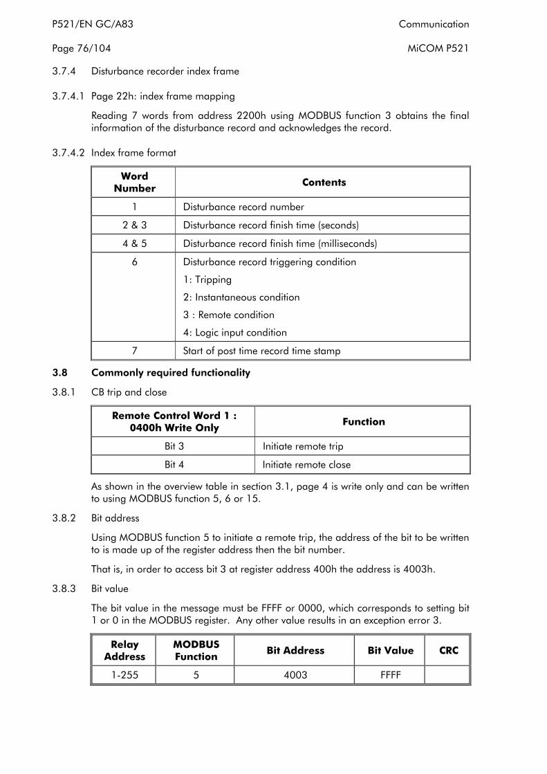
P521/EN GC/A83 Communication Page 76/104 MiCOM P521
3.7.4 Disturbance recorder index frame
3.7.4.1 Page 22h: index frame mapping
Reading 7 words from address 2200h using MODBUS function 3 obtains the final information of the disturbance record and acknowledges the record.
3.7.4.2 Index frame format
Word Number
Contents
1 Disturbance record number
2 & 3 Disturbance record finish time (seconds)
4 & 5 Disturbance record finish time (milliseconds)
6 Disturbance record triggering condition
1: Tripping
2: Instantaneous condition
3 : Remote condition
4: Logic input condition
7 Start of post time record time stamp
3.8 Commonly required functionality
3.8.1 CB trip and close
Remote Control Word 1 : 0400h Write Only
Function
Bit 3 Initiate remote trip
Bit 4 Initiate remote close
As shown in the overview table in section 3.1, page 4 is write only and can be written to using MODBUS function 5, 6 or 15.
3.8.2 Bit address
Using MODBUS function 5 to initiate a remote trip, the address of the bit to be written to is made up of the register address then the bit number.
That is, in order to access bit 3 at register address 400h the address is 4003h.
3.8.3 Bit value
The bit value in the message must be FFFF or 0000, which corresponds to setting bit 1 or 0 in the MODBUS register. Any other value results in an exception error 3.
Relay Address
MODBUS Function
Bit Address Bit Value CRC
1-255 5 4003 FFFF

Communication P521/EN GC/A83 MiCOM P521 Page 77/90
3.8.4 Change setting group
Remote Control Word 1 : 0400h Write Only
Function
Bit 5 Change setting group
As for the previous example, function 5 can be used to write to bit 5 of the control word and change the setting group.
Note: The setting group can only be remotely changed if the ‘change group input’ setting is set to edge.
3.8.4.1 Change setting group request
Relay Address
MODBUS Function
Register Address Command Data
CRC
1-255 5 4005 FFFF
4. IEC 60870-5-103 PROTOCOL
The IEC 60870-5-103 protocol operates a master/slave interface with the relay as the slave. This protocol is based on the VDEW communications protocol and conforms to the IEC 60870-5-103 standard.
A detailed implementation of the protocol is provided in Section 4.3, but an Interoperability statement can be found in Appendix 1.
4.1 Technical characteristics of the IEC 60870-5-103 connection
The connection parameters are:
• Isolated two-point EIA(RS)485 connection (2 kV, 50 Hz)
• Communications baud rates of 9600 or 19200, configurable via the local interfaces
• Communication Parameters of Even Parity, 8 Data Bits and 1 Stop Bit
• Address Range of 1 to 255 (255 as the Broadcast Address), configurable via the local interfaces.
4.2 IEC 60870-5-103 compatible application functions
The following application functions are supported by this interface:
• Initialization (reset)
• Time Synchronization
• Event Record Extraction
• General Interrogation
• Cyclic Measurements
• General Commands
• Disturbance Record Extraction

P521/EN GC/A83 Communication Page 78/104 MiCOM P521
4.3 Application functions
4.3.1 Initialization (reset)
Whenever the relay has been powered up, or if the communications parameters have been changed, a Reset Command is required to initialize the communications. The following two reset commands are supported:
• Reset CU
• Reset FCB
The difference between the two commands is that the Reset CU will clear any unsent messages in the relays transmit buffer and Reset FCB will reset the frame control bit in the connection layer protocol.
The relay will respond to the reset command with the ASDU 5 identification message. The Cause of Transmission value in the message shall be dependent upon the nature of the reset command. The following information will be contained in the data section of this ASDU:
Manufacturers Name and Product Type: MiCOM P
The software identification section of the ASDU 5 message will contain the first four characters of the relay model number to identify the type of relay, and the current software version. The breakdown of the information contained in the data and identification sections can be shown as:
“MiCOM P” + 16bit Model + 8bit Major Version + 1 character Minor Version
e.g. “MiCOM P” + 521 + 3 + ‘A’
In addition to the above identification message, if the relay has been powered up, a power up event will be generated.
4.3.2 Time synchronization
Using the time synchronization feature of the IEC 60870-5-103 protocol allows the relay time and date to be modified. The relay will correct for the transmission delay as specified in the IEC 60870-5-103 standard.
If the time synchronization message is sent as a send/confirm message then the relay will respond with a confirm. If a time synchronization message is sent as either a send/confirm or a send/no reply (broadcast message), a time synchronization message will be returned as Class 1 data.
4.3.3 Event record extraction
The events generated by the relay can be transmitted to the IEC 60870-5-103 master station using either standard information numbers or private information numbers. All standard information numbers are transmitted using the standard function types; all private information numbers are transmitted using private function types.
Therefore the events are categorized using the following information:
• Function Type
• Information Number
Section 5 contains a complete listing of all events produced by the relay.
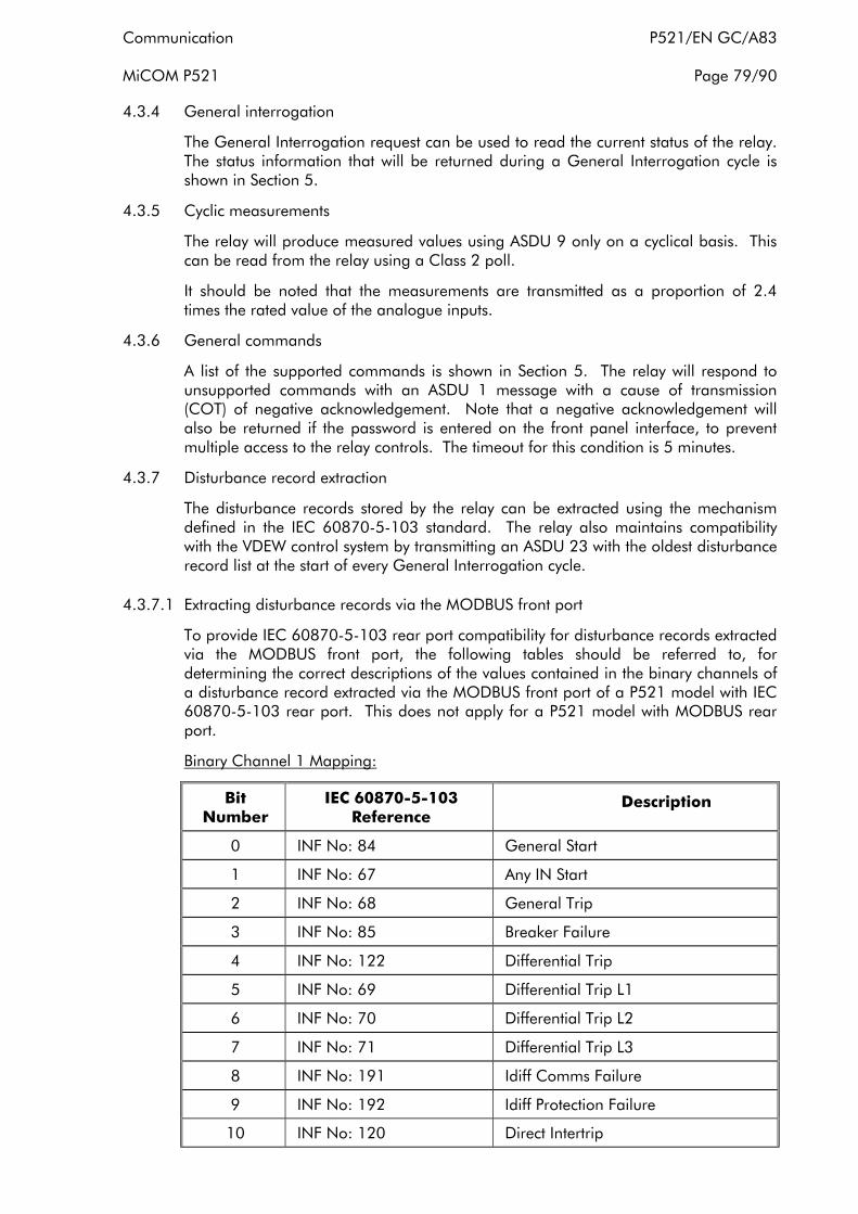
Communication P521/EN GC/A83 MiCOM P521 Page 79/90
4.3.4 General interrogation
The General Interrogation request can be used to read the current status of the relay. The status information that will be returned during a General Interrogation cycle is shown in Section 5.
4.3.5 Cyclic measurements
The relay will produce measured values using ASDU 9 only on a cyclical basis. This can be read from the relay using a Class 2 poll.
It should be noted that the measurements are transmitted as a proportion of 2.4 times the rated value of the analogue inputs.
4.3.6 General commands
A list of the supported commands is shown in Section 5. The relay will respond to unsupported commands with an ASDU 1 message with a cause of transmission (COT) of negative acknowledgement. Note that a negative acknowledgement will also be returned if the password is entered on the front panel interface, to prevent multiple access to the relay controls. The timeout for this condition is 5 minutes.
4.3.7 Disturbance record extraction
The disturbance records stored by the relay can be extracted using the mechanism defined in the IEC 60870-5-103 standard. The relay also maintains compatibility with the VDEW control system by transmitting an ASDU 23 with the oldest disturbance record list at the start of every General Interrogation cycle.
4.3.7.1 Extracting disturbance records via the MODBUS front port
To provide IEC 60870-5-103 rear port compatibility for disturbance records extracted via the MODBUS front port, the following tables should be referred to, for determining the correct descriptions of the values contained in the binary channels of a disturbance record extracted via the MODBUS front port of a P521 model with IEC 60870-5-103 rear port. This does not apply for a P521 model with MODBUS rear port.
Binary Channel 1 Mapping:
Bit Number
IEC 60870-5-103 Reference
Description
0 INF No: 84 General Start
1 INF No: 67 Any IN Start
2 INF No: 68 General Trip
3 INF No: 85 Breaker Failure
4 INF No: 122 Differential Trip
5 INF No: 69 Differential Trip L1
6 INF No: 70 Differential Trip L2
7 INF No: 71 Differential Trip L3
8 INF No: 191 Idiff Comms Failure
9 INF No: 192 Idiff Protection Failure
10 INF No: 120 Direct Intertrip

P521/EN GC/A83 Communication Page 80/104 MiCOM P521
Bit Number
IEC 60870-5-103 Reference
Description
11 INF No: 121 Permissive Intertrip Trip
12 INF No: 123 Idiff Intertrip
13 INF No: 90 I> Trip
14 INF No: 91 I>> Trip
15 INF No: 94 I>>> Trip
Binary Channel 2 Mapping:
Bit number
IEC 60870-5-103 reference
Description
0 INF No: 95 I>>>> Trip
1 INF No: 92 IN> Trip
2 INF No: 93 IN>> Trip
3 INF No: 96 IN>>> Trip
4 INF No: 97 IN>>>> Trip
5 INF No: 161 Logic Input 1
6 INF No: 162 Logic Input 2
7 INF No: 163 Logic Input 3
8 INF No: 164 Logic Input 4
9 INF No: 165 Logic Input 5
10 Reserved Reserved
11 Reserved Reserved
12 Reserved Reserved
13 Reserved Reserved
14 Reserved Reserved
15 Reserved Reserved
4.3.8 Blocking of monitor direction
The relay does not support the facility to Block Messages in the Monitor direction.
4.3.9 Test mode
The relay does not support the Test Mode function.

Communication P521/EN GC/A83 MiCOM P521 Page 81/90
5. IEC 60870-5-103 DETAILED IMPLEMENTATION
5.1 Compatible range information numbers in monitor direction
ASDU TYPE
COT FUN INF NO.
Description GI Interpretation
System Functions
8 10 255 0 End of General Interrogation
6 8 255 0 Time Synchronization
5 3 192 2 Reset FCB
5 4 192 3 Reset CU
5 5 192 4 Start/Restart
5 6 192 5 Power On
Status Indication
1 12,20,21 192 19 LED Reset Indications and Latches Reset
1 9,12 192 22 Local Parameter Setting * Password Entered Locally
1 9,12,20,21 192 23 Characteristic 1 * Setting Group 1 Changed
1 9,12,20,21 192 24 Characteristic 2 * Setting Group 2 Changed
1 1,9 192 27 Auxiliary Input 1 * Auxiliary 1 Timer Expiry
1 1,9 192 28 Auxiliary Input 2 * Auxiliary 2 Timer Expiry
Supervision Indications
1 1,9 192 36 Trip Circuit Supervision * Trip Circuit Supervision Trip
Fault Indications
2 1,9 192 64 Start /Pickup L1 * Differential Start L1
2 1,9 192 65 Start /Pickup L2 * Differential Start L2
2 1,9 192 66 Start /Pickup L3 * Differential Start L3
2 1,9 192 67 Start /Pickup N * Any IN Start
2 1 192 68 General Trip Any Trip
2 1 192 69 Trip L1 Differential Trip L1
2 1 192 70 Trip L2 Differential Trip L2
2 1 192 71 Trip L3 Differential Trip L3
2 1,9 192 84 General Start * Any Start
1 1 192 85 Breaker Failure Breaker Failure (tBF)
2 1 192 90 Trip I> I> Overcurrent Trip
2 1 192 91 Trip I>> I>> Overcurrent Trip
2 1 192 92 Trip IN> IN> Overcurrent Trip
2 1 192 93 Trip IN>> IN>> Overcurrent Trip
2 1,9 192 94 Equation A
2 1,9 192 95 Equation B
2 1,9 192 96 Equation C
2 1,9 192 97 Equation D
2 1,9 192 98 Equation E
2 1,9 192 99 Equation F
2 1,9 192 100 Equation G
2 1,9 192 101 Equation H

P521/EN GC/A83 Communication Page 82/104 MiCOM P521
ASDU TYPE
COT FUN INF NO.
Description GI Interpretation
2 1 192 102 Inter-Trip 1
2 1 192 103 Inter-Trip 2
2 1 192 104 Inter-Trip 3
2 1 192 105 Inter-Trip 4
1 1,9 192 106 Local Inrush Block
1 1,9 192 107 Local Phase A Block
1 1,9 192 108 Local Phase B Block
1 1,9 192 109 Local Phase C Block
1 1,9 192 110 Remote Inrush Block
1 1,9 192 111 Remotel Phase A Block
1 1,9 192 112 Remotel Phase B Block
1 1,9 192 113 Remotel Phase C Block
1 1,9 192 114 Inrush Block Configure Error
1 1,9 192 115 CTS Cdiff Block
1 1,9 192 116 Local CTS Fail
1 1,9 192 117 Remote CTS Fail
1 1,9 192 118 CTS Block
1 1,9 192 119 CTS Cdiff Restrain
1 1,9 192 120 CTS Inhibited
1 1,9 192 121 CTS Conf Fail
1 1,9 192 122 Convention Mode
1 1,9 192 123 Time Synchronization
1 1 192 124 reset led
1 1 192 125 cortec mismatch
1 1 192 126 Conf Conflict Comms
Measurands
9 2 192 148 Measurands IL1,2,3,VL1,2,3,P,Q,f
Measurement = 2.4 x Rated Value

Communication P521/EN GC/A83 MiCOM P521 Page 83/90
5.2 Compatible range information numbers in control direction
ASDU TYPE
COT FUN INF NO.
Description GI Interpretation
System Functions
7 9 255 0 Init. General Interrogation
6 8 255 0 Time Synchronization
General Commands
20 20 192 19 LED Reset Reset Indications and Latches
20 20 192 23 Characteristic 1 6 Activate Setting Group 1
20 20 192 24 Characteristic 2 7 Activate Setting Group 2
5.3 Private range information numbers in monitor direction
ASDU TYPE
COT FUN INF NO.
Description GI Interpretation
Fault Indications
2 1 194 94 Trip I>>> I>>> Overcurrent Trip
2 1 194 95 Trip I>>>> I>>>> Overcurrent Trip
2 1 194 96 Trip IN>>> IN>>> Overcurrent Trip
2 1 194 97 Trip IN>>>> IN>>>> Overcurrent Trip
2 1,9 194 98 Start I> * I> Overcurrent Start
2 1,9 194 99 Start I>> * I>> Overcurrent Start
2 1,9 194 100 Start I>>> * I>>> Overcurrent Start
2 1,9 194 101 Start I>>>> * I>>>> Overcurrent Start
2 1,9 194 102 Start IN> * IN> Overcurrent Start
2 1,9 194 103 Start IN>> * IN>> Overcurrent Start
2 1,9 194 104 Start IN>>> * IN>>> Overcurrent Start
2 1,9 194 105 Start IN>>>> * IN>>>> Overcurrent Start
2 1,9 194 106 Start I< * I< Undercurrent Start
2 1 194 107 Trip I< I< Undercurrent Trip
2 1,9 194 108 Start I2> * I2> Negative Sequence Start
2 1 194 109 Trip I2> I2> Negative Sequence Trip
2 1,9 194 110 Start I2>> * I2>> Negative Sequence Start
2 1 194 111 Trip I2>> I2>> Negative Sequence Trip
2 1,9 194 112 Alarm Thermal * Thermal Overload Alarm
2 1 194 113 Trip Thermal Thermal Overload Trip
2 1 194 114 Broken Conductor Broken Conductor Trip
1 1 194 120 CH1 Direct Intertrip Direct Intertrip Received on CH1
2 1 194 121 CH1 Permissive Intertrip Trip Permissive Intertrip Trip from CH1
2 1 194 122 Current Differential Trip Current Diff Trip
6 Must be in Edge Mode.
7 Must be in Edge Mode.

P521/EN GC/A83 Communication Page 84/104 MiCOM P521
ASDU TYPE
COT FUN INF NO.
Description GI Interpretation
Fault Indications
1 1 194 123 CH1 IDiff Intertrip Current Diff Intertrip RX on CH1
2 1,9 194 124 CH1 Permissive Intertrip Start * Permissive Intertrip Start from CH1
Relay Indications
1 1,9 194 140 CB Closed * CB Change of State - Closed State
1 1,9 194 141 CB Open * CB Change of State - Open State
1 12,20,21 194 142 Remote CB Trip Remote CB Trip Acknowledged
1 12,20,21 194 143 Remote CB Close Remote CB Close Acknowledged
Logical Statuses
1 1,9 194 161 Logic Input 1 * Change of Logic Input 1 State
1 1,9 194 162 Logic Input 2 * Change of Logic Input 2 State
1 1,9 194 163 Logic Input 3 * Change of Logic Input 3 State
1 1,9 194 164 Logic Input 4 * Change of Logic Input 4 State
1 1,9 194 165 Logic Input 5 * Change of Logic Input 5 State
1 1,9 194 176 Relay Contact 0 * Change of Trip Relay State
1 1,9 194 177 Relay Contact 1 * Change of Relay Output 1 State
1 1,9 194 178 Relay Contact 2 * Change of Relay Output 2 State
1 1,9 194 179 Relay Contact 3 * Change of Relay Output 3 State
1 1,9 194 180 Relay Contact 4 * Change of Watchdog Relay State
1 1,9 194 181 Relay Contact 5 * Change of Relay Output 5 State
1 1,9 194 182 Relay Contact 6 * Change of Relay Output 6 State
1 1,9 194 183 Relay Contact 7 * Change of Relay Output 7 State
1 1,9 194 184 Relay Contact 8 * Change of Relay Output 8 State
Alarm Indications
1 1,9 194 190 IDiff CH1 Comms Alarm * CH1 Protection Comms Alarm
1 1,9 194 191 IDiff Comms Failure * Total Protection Comms Failure
1 1,9 194 192 IDiff Protection Failure * Current Diff Protection Failure
1 1,9 194 193 Backup Protection Active * Overcurrent Backup Protection Active
1 1,9 194 195 Output Contacts Disabled * Commissioning Mode
1 1,9 194 196 Loopback Mode Selected * Commissioning Mode
1 1,9 194 197 IDiff Protection Disabled * Current Diff Protection Disabled
1 1,9 194 198 CB Status DBI * CB Fail
5.4 Private range information numbers in control direction
ASDU TYPE
COT FUN Description GI Interpretation
General Commands
20 20 194 142 Remote CB Trip Perform a Remote CB Trip
20 20 194 143 Remote CB Close Perform a Remote CB Close

Communication P521/EN GC/A83 MiCOM P521 Page 85/90
6. DNP3.0 INTRODUCTION
6.1 Purpose of this document
The purpose of this document is to describe the specific implementation of the Distributed Network Protocol (DNP) 3.0 within P521 MiCOM relay.
P521 uses the Triangle MicroWorks, Inc. DNP 3.0 Slave Source Code Library Version 2.18.
This document, in conjunction with the DNP 3.0 Basic 4 Document Set, and the DNP Subset Definitions Document, provides complete information on how to communicate with P521 via the DNP 3.0 protocol.
This implementation of DNP 3.0 is fully compliant with DNP 3.0 Subset Definition Level 2, contains many Subset Level 3 features, and contains some functionality even beyond Subset Level 3.
6.2 DNP V3.00 device profile
The following table provides a “Device Profile Document” in the standard format defined in the DNP 3.0 Subset Definitions Document. While it is referred to in the DNP 3.0 Subset Definitions as a “Document,” it is only a component of a total interoperability guide. This table, in combination with the following should provide a complete interoperability/configuration guide for P521:
• The Implementation Table provided in Section 6.3 (beginning on page 72),
• The Point List Tables provided in Section 6.4 (beginning on page 77),
• And a description of configuration methods and user-interface in Sections

P521/EN GC/A83 Communication Page 86/104 MiCOM P521
DNP 3.0 Device Profile Document
(Also see the implementation table in section 6.3, beginning on page 72)
Vendor Name: Schneider Electric T&D – Energy Automation and Information Systems
Device Name: SERIAL 20 Platform using the Triangle MicroWorks, Inc. DNP 3.0 Slave
Source Code Library, Version 2.18.
Highest DNP Level Supported: For Requests: Level 2 For Responses: Level 2
Device Function:
Master
Slave
Notable objects, functions, and/or qualifiers supported in addition to the highest DNP levels supported (the complete list is described in the DNP 3.0 Implementation Table):
For static (non-change event) object requests, request qualifier codes 00 and 01 (start-stop), 07 and 08 (limited quantity), and 17 and 28 (index) are supported in addition to the request qualifier code 06 (no range (all points). Static object requests sent with qualifiers 00, 01, 06, 07, or 08 will be responded with qualifiers 00 or 01. Static object requests sent with qualifiers 17 or 28 will be responded with qualifiers 17 or 28. For change-event object requests, qualifiers 17 or 28 are always responded 16-bit and 32-bit analog change events with time may be requested. The read function code for Object 50 (time and date) variation 1 is supported
Maximum Data Link Frame Size (octets): Transmitted: 292 Received: 292
Maximum Application Fragment Size (octets) Transmitted: 2048 Received: 2048
Maximum Data Link Retries: . None Fixed at 2 Configurable
Maximum Application Layer Retries: None . Configurable
Requires Data Link Layer Confirmation: Never Always Sometimes Configurable
Requires Application Layer Confirmation: Never Always When reporting event data When sending multi-fragment responses Sometimes Configurable

Communication P521/EN GC/A83 MiCOM P521 Page 87/90
DNP 3.0 Device Profile Document
(Also see the implementation table in section 6.3, beginning on page 72)
Timeouts while waiting for:
Data Link Confirm: None Fixed at 100ms Variable Configurable
Complete Appl. Fragment: None Fixed at ___ Variable Configurable
Application Confirm: None Fixed at 1s ___ Variable Configurable
Complete Appl. Response: None Fixed at ___ Variable Configurable
Others:
Binary input change scanning period: 5ms
Analogue input change scanning period: 1s
Sends/Executes Control Operations:
Write Binary Outputs: Never Always Sometimes Configurable
Select/Operate: Never Always Sometimes Configurable
Direct Operate: Never Always Sometimes Configurable
Direct Operate – No Ack: Never Always Sometimes Configurable
Count > 1 Never Always Sometimes Configurable
Pulse On/NUL/Trip/Close Never Always Sometimes Configurable
Pulse Off/NUL/Trip/Close Never Always Sometimes Configurable
Latch On/NUL Never Always Sometimes Configurable
Latch Off/NUL Never Always Sometimes Configurable
Queue Never Always Sometimes Configurable
Clear Queue Never Always Sometimes Configurable
Reports Binary Input Change Events when no specific variation requested: Never Only time-tagged Only non-time-tagged Configurable
Reports time-tagged Binary Input Change Events when no specific variation requested: Never Binary input change with time Binary input change with relative
time Configurable

P521/EN GC/A83 Communication Page 88/104 MiCOM P521
DNP 3.0 Device Profile Document
(Also see the implementation table in section 6.3, beginning on page 72)
Sends Unsolicited Responses: Never Configurable Certain objects only Sometimes Enable/Disable unsolicited functions
codes supported
Sends Static Data in Unsolicited Responses: Never When device restarts When status flags changes
No other options are permitted
Default Counter Object/Variation:
No counters reported
Configurable
Default object: 20
Default variation: 5
Point-by-point list attached
Counters Roll Over at:
No counters reported
Configurable
16 bits
32 bits
Other value: _____
Point-by-point list attached
Sends multi-fragment responses:
Yes
No
6.3 Implementation Table
The following table identifies the variations, function codes, and qualifiers supported by the P521 in both request and response messages.
In the table below the text shaded as indicates Subset Level 3 functionality (beyond Subset Level 2), and text shaded as Indicates functionality beyond Subset Level 3.
Subset Level 3
Subset Level 3

Communication P521/EN GC/A83 MiCOM P521 Page 89/90
Object Request Response
Object Number
Variation Number Description Function Codes
(Dec) Qualifier Codes
(Hex) Function
Codes (Dec) Qualifier Codes
(Hex)
1 0 Binary Input (Variation 0 is used to request default variation)
1 (read) 00, 01
06
07, 08
17, 28
(start-stop)
(no range, or all)
limited qty)
(index)
1 1
(default - see note 1)
Binary Input 1 (read) 00, 01
06
07, 08
17, 28
(start-stop)
(no range, or all)
limited qty)
(index)
129 response 00, 01
17, 28
(start-stop)
(index - see note 2)
1 2 Binary Input with status 1 (read) 00, 01
06
07, 08
17, 28
(start-stop)
(no range, or all)
limited qty)
(index)
129 response 00, 01
17, 28
(start-stop)
(index - see note 2)
2 0 Binary Input Change (Variation 0 is used to request default variation)
1 (read) 06
07, 08
(no range, or all)
(limited qty)
2 1 Binary Input Change without Time
1 (read) 06
07, 08
(no range, or all)
(limited qty)
129 response 17, 28 (index)
2 2
(default - see note 1)
Binary Input Change with Time
1 (read) 06
07, 08
(no range, or all)
(limited qty)
129 response 17, 28 (index)
10 0 Binary Output Status (Variation 0 is used to request default variation)
1 (read) 00, 01
06
07, 08
17, 28
(start-stop)
(no range, or all)
limited qty)
(index)
10 2
(default - see note 1)
Binary Output Status 1 (read) 00, 01
06
07, 08
17, 28
(start-stop)
(no range, or all)
limited qty)
(index)
129 response 00, 01
17, 28
(start-stop)
(index - see note 2)
12 1 Control Relay Output Block
3
4
5
6
(select)
(operate)
(direct op)
(dir. op, no ack)
00, 01
06
07, 08
17, 28
(start-stop)
(limited qty)
(index)
129 response echo of request
20 0 Binary Counter (Variation 0 is used to request default variation)
1
7
8
9
10
(read)
(freeze)
(freeze no ack)
(freeze clear)
(frz. cl. no ack)
00, 01
06
07, 08
17, 28
(start-stop)
(no range, or all)
limited qty)
(index)
20 1 32-Bit Binary Counter with Flag
1
7
8
9
10
(read)
(freeze)
(freeze no ack)
(freeze clear)
(frz. cl. no ack)
00, 01
06
07, 08
17, 28
(start-stop)
(no range, or all)
limited qty)
(index)
129 response 00, 01
17, 28
(start-stop)
(index - see note 2)
20 2 16-Bit Binary Counter with Flag
1
7
8
9
10
(read)
(freeze)
(freeze no ack)
(freeze clear)
(frz. cl. no ack)
00, 01
06
07, 08
17, 28
(start-stop)
(no range, or all)
limited qty)
(index)
129 response 00, 01
17, 28
(start-stop)
(index - see note 2)
20 5
(default - see note 1)
32-Bit Binary Counter without Flag
1
7
8
9
10
(read)
(freeze)
(freeze no ack)
(freeze clear)
(frz. cl. no ack)
00, 01
06
07, 08
17, 28
(start-stop)
(no range, or all)
limited qty)
(index)
129 response 00, 01
17, 28
(start-stop)
(index - see note 2)

P521/EN GC/A83 Communication Page 90/104 MiCOM P521
Object Request Response
Object Number
Variation Number Description Function Codes
(Dec) Qualifier Codes
(Hex) Function
Codes (Dec) Qualifier Codes
(Hex)
20 6 16-Bit Binary Counter without Flag
1
7
8
9
10
(read)
(freeze)
(freeze no ack)
(freeze clear)
(frz. cl. no ack)
00, 01
06
07, 08
17, 28
(start-stop)
(no range, or all)
limited qty)
(index)
129 response 00, 01
17, 28
(start-stop)
(index - see note 2)
21 0 Frozen Counter (Variation 0 is used to request default variation)
1 (read) 00, 01
06
07, 08
17, 28
(start-stop)
(no range, or all)
limited qty)
(index)
21 1 32-Bit Frozen Counter with Flag
1 (read) 00, 01
06
07, 08
17, 28
(start-stop)
(no range, or all)
limited qty)
(index)
129 response 00, 01
17, 28
(start-stop)
(index - see note 2)
21 2 16-Bit Frozen Counter with Flag
1 (read) 00, 01
06
07, 08
17, 28
(start-stop)
(no range, or all)
limited qty)
(index)
129 response 00, 01
17, 28
(start-stop)
(index - see note 2)
21 9
(default - see note 1)
32-Bit Frozen Counter without Flag
1 (read) 00, 01
06
07, 08
17, 28
(start-stop)
(no range, or all)
limited qty)
(index)
129 response 00, 01
17, 28
(start-stop)
(index - see note 2)
21 10 16-Bit Frozen Counter without Flag
1 (read) 00, 01
06
07, 08
17, 28
(start-stop)
(no range, or all)
limited qty)
(index)
129 response 00, 01
17, 28
(start-stop)
(index - see note 2)
30 0 Analog Input (Variation 0 is used to request default variation)
1 (read) 00, 01
06
07, 08
17, 28
(start-stop)
(no range, or all)
limited qty)
(index)
30 1
(default - see note 1)
32-Bit Analog Input 1 (read) 00, 01
06
07, 08
17, 28
(start-stop)
(no range, or all)
limited qty)
(index)
129 response 00, 01
17, 28
(start-stop)
(index - see note 2)
30 2
(default - see note 1)
16-Bit Analog Input 1 (read) 00, 01
06
07, 08
17, 28
(start-stop)
(no range, or all)
limited qty)
(index)
129 response 00, 01
17, 28
(start-stop)
(index - see note 2)
30 3 32-Bit Analog Input without Flag
1 (read) 00, 01
06
07, 08
17, 28
(start-stop)
(no range, or all)
limited qty)
(index)
129 response 00, 01
17, 28
(start-stop)
(index - see note 2)
30 4 16-Bit Analog Input without Flag
1 (read) 00, 01
06
07, 08
17, 28
(start-stop)
(no range, or all)
limited qty)
(index)
129 response 00, 01
17, 28
(start-stop)
(index - see note 2)
32 0 Analog Change Event (Variation 0 is used to request default variation)
1 (read) 06
07, 08
(no range, or all)
(limited qty)
32 1 32-Bit Analog Change Event without Time
1 (read) 06
07, 08
(no range, or all)
(limited qty)
129 response 17, 28 (index)
32 2
(default - see note 1)
16-Bit Analog Change Event without Time
1 (read) 06
07, 08
(no range, or all)
(limited qty)
129 response 17, 28 (index)

Communication P521/EN GC/A83 MiCOM P521 Page 91/90
Object Request Response
Object Number
Variation Number Description Function Codes
(Dec) Qualifier Codes
(Hex) Function
Codes (Dec) Qualifier Codes
(Hex)
32 3 32-Bit Analog Change Event with Time
1 (read) 06
07, 08
(no range, or all)
(limited qty)
129 response 17, 28 (index)
32 4 16-Bit Analog Change Event with Time
1 (read) 06
07, 08
(no range, or all)
(limited qty)
129 response 17, 28 (index)
50 0 Time and Date 1 (read) 00, 01
06
07, 08
17, 28
(start-stop)
(no range, or all)
limited qty)
(index)
129 response 00, 01
17, 28
(start-stop)
(index - see note 2)
50 1
(default - see note 1)
Time and Date 1
2
(read)
(write)
00, 01
06
07
08
17, 28
(start-stop)
(no range, or all)
(limited qty = 1)
(limited qty)
(index)
129 response 00, 01
17, 28
(start-stop)
(index - see note 2)
52 2 Time Delay Fine 129 response 07 (limited qty)
(qty = 1)
60 0 Class 0, 1, 2, and 3 Data
1 (read) 06 (no range, or all)
60 1 Class 0 Data 1 (read) 06 (no range, or all) 129 response 17, 28 (index)
60 2 Class 1 Data 1 (read) 06
07, 08
(no range, or all)
(limited qty)
129 response 17, 28 (index)
60 3 Class 2 Data 1 (read) 06
07, 08
(no range, or all)
(limited qty)
129 response 17, 28 (index)
60 4 Class 3 Data 1 (read) 06
07, 08
(no range, or all)
(limited qty)
129 response 17, 28 (index)
80 1 Internal Indications 2 (write) 00 (start–stop) (index must = 7)
No Object (function code only)
13 (cold restart)
No Object (function code only)
14 (warm restart)
No Object (function code only)
23 (delay meas.)
Note 1: A Default variation refers to the variation responded when
variation 0 is requested and/or in class 0, 1, 2, or 3 scans.
Note 2: For static (non-change-event) objects, qualifiers 17 or 28 are only responded when a request is sent with qualifiers 17 or 28, respectively. Otherwise, static object requests sent with qualifiers 00, 01, 06, 07, or 08, will be responded with qualifiers 00 or 01. (For change-event objects, qualifiers 17 or 28 are always responded.)
Note 3: For P521, a cold restart is implemented as a warm restart – the
executable is not restarted, but the DNP process is restarted.

P521/EN GC/A83 Communication Page 92/104 MiCOM P521
6.4 Point list
The tables in the following sections identify all the individual data points provided by this implementation of DNP 3.0.
6.4.1 Binary input points
Every Binary Input Status points are included in class 0 polls, because they are included in one of classes 1, 2 or 3.
Binary Input Points
Static (Steady-State) Object Number: 1 Change Event Object Number: 2 Request Function Codes supported: 1 (read) Static Variation reported when variation 0 requested: 1 (Binary input without status) Change Event Variation reported when variation 0 requested: 2 (Binary input change with time)
P521Point Index
Name/Description
Latched Alarm
(See Note 1)
Initial Value
Change Event Class (1, 2, 3, or
none)
Inputs and Outputs
0 Output Relay 1 (Trip) 0 1
1 Output Relay 2 0 2
2 Output Relay 3 0 2
3 Output Relay 4 0 2
4 Output Relay 0 (Watchdog) 0 2
5 Output Relay 5 0 2
6 Output Relay 6 0 2
7 Output Relay 7 0 2
8 Output Relay 8 0 2
9 Logic Input 1 0 2
10 Logic Input 2 0 2
11 Logic Input 3 0 2
12 Logic Input 4 0 2
13 Logic Input 5 0 2
Protection
14 Current Differential Start 0 1
15 Current Differential Trip 0 1
16 Current Differential Intertrip Received 0 1
17 Permissive Intertrip Start 0 1
18 Permissive Intertrip Trip 0 1
19 Direct Intertrip Received 0 1
20 Phase Overcurrent 1st Stage Start (I>) 0 1
21 Phase Overcurrent 1st Stage Trip (tI>) 0 1
22 Phase Overcurrent 2nd Stage Start (I>>) 0 1
23 Phase Overcurrent 2nd Stage Trip (tI>>) 0 1

Communication P521/EN GC/A83 MiCOM P521 Page 93/90
Binary Input Points
Static (Steady-State) Object Number: 1 Change Event Object Number: 2 Request Function Codes supported: 1 (read) Static Variation reported when variation 0 requested: 1 (Binary input without status) Change Event Variation reported when variation 0 requested: 2 (Binary input change with time)
P521Point Index
Name/Description
Latched Alarm
(See Note 1)
Initial Value
Change Event Class (1, 2, 3, or
none)
24 Phase Overcurrent 3rd Stage Start (I>>>)
0 1
25 Phase Overcurrent 3rd Stage Trip (tI>>>)
0 1
26 Phase Overcurrent 4th Stage Start (I>>>>)
0 1
27 Phase Overcurrent 4th Stage Trip (tI>>>>)
0 1
28 Earth Overcurrent 1st Stage Start (Ie>) 0 1
29 Earth Overcurrent 1st Stage Trip (tIe>) 0 1
30 Earth Overcurrent 2nd Stage Start (Ie>>) 0 1
31 Earth Overcurrent 2nd Stage Trip (tIe>>) 0 1
32 Earth Overcurrent 3rd Stage Start (Ie>>>)
0 1
33 Earth Overcurrent 3rd Stage Trip (tIe>>>)
0 1
34 Earth Overcurrent 4th Stage Start (Ie>>>>)
0 1
35 Earth Overcurrent 4th Stage Trip (tIe>>>>)
0 1
36 Undercurrent Start (I<) 0 1
37 Undercurrent Trip (tI<) 0 1
38 Negative Sequence 1st Stage Start (I2>) 0 1
39 Negative Sequence 1st Stage Trip (tI2>) 0 1
40 Negative Sequence 2nd Stage Start (I2>>)
0 1
41 Negative Sequence 2nd Stage Trip (tI2>>)
0 1
42 Thermal Start 0 1
43 Thermal Trip 0 1
44 Broken Conductor 0 1
Non-Protection Functions
45 Auxiliary Timer 1 (tAux1) 0 1
46 Auxiliary Timer 2 (tAux2) 0 1
47 Logic Select Timer Enabled (tSEL1) 0 1
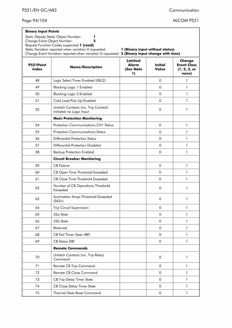
P521/EN GC/A83 Communication Page 94/104 MiCOM P521
Binary Input Points
Static (Steady-State) Object Number: 1 Change Event Object Number: 2 Request Function Codes supported: 1 (read) Static Variation reported when variation 0 requested: 1 (Binary input without status) Change Event Variation reported when variation 0 requested: 2 (Binary input change with time)
P521Point Index
Name/Description
Latched Alarm
(See Note 1)
Initial Value
Change Event Class (1, 2, 3, or
none)
48 Logic Select Timer Enabled (tSEL2) 0 1
49 Blocking Logic 1 Enabled 0 1
50 Blocking Logic 2 Enabled 0 1
51 Cold Load Pick-Up Enabled 0 1
52 Unlatch Contacts (inc. Trip Contact) Initiated via Logic Input
0 1
Main Protection Monitoring
54 Protection Communications CH1 Status 0 1
55 Protection Communications Status 0 1
56 Differential Protection Status 0 1
57 Differential Protection Disabled 0 1
58 Backup Protection Enabled 0 1
Circuit Breaker Monitoring
59 CB Failure 0 1
60 CB Open Time Threshold Exceeded 0 1
61 CB Close Time Threshold Exceeded 0 1
62 Number of CB Operations Threshold Exceeded
0 1
63 Summation Amps Threshold Exceeded (SA2n)
0 1
64 Trip Circuit Supervision 0 1
65 52a State 0 1
66 52b State 0 1
67 Reserved 0 1
68 CB Fail Timer State (tBF) 0 1
69 CB Status DBI 0 1 Remote Commands
70 Unlatch Contacts (inc. Trip Relay) Command
0 1
71 Remote CB Trip Command 0 1
72 Remote CB Close Command 0 1
73 CB Trip Delay Timer State 0 1
74 CB Close Delay Timer State 0 1
75 Thermal State Reset Command 0 1

Communication P521/EN GC/A83 MiCOM P521 Page 95/90
Binary Input Points
Static (Steady-State) Object Number: 1 Change Event Object Number: 2 Request Function Codes supported: 1 (read) Static Variation reported when variation 0 requested: 1 (Binary input without status) Change Event Variation reported when variation 0 requested: 2 (Binary input change with time)
P521Point Index
Name/Description
Latched Alarm
(See Note 1)
Initial Value
Change Event Class (1, 2, 3, or
none)
Hardware Status Monitoring
77 Major Hardware Alarm Present 0 1
78 Minor Hardware Alarm Present 0 1
Latched Alarms
79 Current Differential Trip * 0 3
80 Current Differential Intertrip Received * 0 3
81 Permissive Intertrip Trip * 0 3
82 Direct Intertrip Received * 0 3
83 Phase Overcurrent 1st Stage Trip (tI>) * 0 3
84 Phase Overcurrent 2nd Stage Trip (tI>>) * 0 3
85 Phase Overcurrent 3rd Stage Trip (tI>>>)
* 0 3
86 Phase Overcurrent 4th Stage Trip (tI>>>>)
* 0 3
87 Earth Overcurrent 1st Stage Trip (tIe>) * 0 3
88 Earth Overcurrent 2nd Stage Trip (tIe>>) * 0 3
89 Earth Overcurrent 3rd Stage Trip (tIe>>>) * 0 3
90 Earth Overcurrent 4th Stage Trip (tIe>>>>) * 0 3
91 Undercurrent Trip (tI<) * 0 3
92 Negative Sequence 1st Stage Trip (tI2>) * 0 3
93 Negative Sequence 2nd Stage Trip (tI2>>)
* 0 3
94 Thermal Start * 0 3
95 Thermal Trip * 0 3
96 Auxiliary Timer 1 (tAux1) * 0 3
97 Auxiliary Timer 2 (tAux2) * 0 3
98 Broken Conductor * 0 3
99 Protection Communications CH1 Status * 0 3
100 Differential Protection Status * 0 3
101 Differential Protection Disabled * 0 3
102 CB Failure * 0 3

P521/EN GC/A83 Communication Page 96/104 MiCOM P521
Binary Input Points
Static (Steady-State) Object Number: 1 Change Event Object Number: 2 Request Function Codes supported: 1 (read) Static Variation reported when variation 0 requested: 1 (Binary input without status) Change Event Variation reported when variation 0 requested: 2 (Binary input change with time)
P521Point Index
Name/Description
Latched Alarm
(See Note 1)
Initial Value
Change Event Class (1, 2, 3, or
none)
103 CB Open Time Threshold Exceeded * 0 3
104 CB Close Time Threshold Exceeded * 0 3
105 Number of CB Operations Threshold Exceeded
* 0 3
106 Summation Amps Threshold Exceeded (SA2n)
* 0 3
107 Trip Circuit Supervision * 0 3
108 CB Status DBI * 0 3
109 Equation A 0 1
110 Equation B 0 1
111 Equation C 0 1
112 Equation D 0 1
113 Equation E 0 1
114 Equation F 0 1
115 Equation G 0 1
116 Equation H 0 1
117 Inter-Trip 1 0 1
118 Inter-Trip 2 0 1
119 Inter-Trip 3 0 1
120 Inter-Trip 4 0 1
121 Local Inrush Block 0 1
122 Local Phase A Block 0 1
123 Local Phase B Block 0 1
124 Local Phase C Block 0 1
125 Remote Inrush Block 0 1
126 Remote Phase A Block 0 1
127 Remote Phase B Block 0 1
128 Remote Phase C Block 0 1
129 Inrush Block Configure Error 0 1
130 Local CTS Fail 0 1
131 Remote CTS Fail 0 1
132 CTS Block 0 1
133 CTS Cdiff Block 0 1
134 CTS Cdiff Restrain 0 1
135 CTS Inhibited 0 1

Communication P521/EN GC/A83 MiCOM P521 Page 97/90
Binary Input Points
Static (Steady-State) Object Number: 1 Change Event Object Number: 2 Request Function Codes supported: 1 (read) Static Variation reported when variation 0 requested: 1 (Binary input without status) Change Event Variation reported when variation 0 requested: 2 (Binary input change with time)
P521Point Index
Name/Description
Latched Alarm
(See Note 1)
Initial Value
Change Event Class (1, 2, 3, or
none)
136 CTS Conf Fail 0 1
137 Equation A Alarm 0 3
138 Equation B Alarm 0 3
139 Equation C Alarm 0 3
140 Equation D Alarm 0 3
141 Equation E Alarm 0 3
142 Equation F Alarm 0 3
143 Equation G Alarm 0 3
144 Equation H Alarm 0 3
145 Inrush Block Alarm 0 3
146 Local CTS Fail Alarm 0 3
147 Remote CTS Fail Alarm 0 3
148 CTS Block Alarm 0 3
149 CTS Cdiff Block Alarm 0 3
150 CTS Cdiff Restrain Alarm 0 3
151 CTS Inhibited Alarm 0 3
152 CTS Conf Fail Alarm 0 3
153 Led Reset 0 3
154 Convention Mode 0 3
155 Time Synchronization 0 3
156 Conf Conflict Comms 0 1
Note 1:, Points marked as Latched Alarms are latched on when the condition has occurred and not cleared until the alarms are acknowledged (cleared) via the Remote Communications or Front Panel Interface. Note that if the Alarm is an auto-clear type then the alarm will automatically be removed when the condition is cleared (Controlled via the Auto Alarm acknowledgement Setting in the Configuration Menu). Points not marked as Latched Alarms shall follow the state of the relevant condition (real-time value).

P521/EN GC/A83 Communication Page 98/104 MiCOM P521
6.4.2 Binary output status points and control relay output block
The following table lists both the Binary Output Status Points (Object 10) and the Control Relay Output Block (Object 12). Binary Output Status Points are not included in class 0 polls.
Binary Output Status Points
Object Number: 10
Request Function Code supported: 1 (read)
Default Variation reported when variation 0 requested: 2 (Binary Output Status)
Control Relay Output Blocks (CROB)
Object Number: 12
Request Function Code supported: 5 (direct operate), 6 (direct operate, Nack)
P521Point Index
Name/Description Initial Value Include in Class 0 Poll
Supported CROB Fields
0 Reset All Latched Contacts (inc Trip Contact) 0 Yes
Pulse On/Trip/Close /Unpaired
1 Acknowledge First Alarm Only 0 Yes Pulse On/Trip/Close /Unpaired
2 Acknowledge All Alarms 0 Yes Pulse On/Trip/Close /Unpaired
3 Remote CB Trip Command 0 Yes Pulse On/Trip/Unpaired
4 Remote CB Close Command 0 Yes Pulse On/Close/Unpaired
5 Cancel CB Trip 0 Yes Pulse On/Trip/Close /Unpaired
6 Cancel CB Close 0 Yes Pulse On/Trip/Close /Unpaired
7 Setting Goup Change (See Note 2) 0 Yes
Pulse On/Trip/Close /Unpaired
8 Thermal State Reset 0 Yes Pulse On/Trip/Close /Unpaired
9 Reset Average and Max Measurements 0 Yes
Pulse On/Trip/Close /Unpaired
10 Reset Rolling Average Measurements 0 Yes
Pulse On/Trip/Close
/Unpaired
11 Reset Rolling Max Measurements 0 Yes Pulse On/Trip/Close /Unpaired
12 Reset Protection Communications Statistics
0 Yes Pulse On/Trip/Close /Unpaired
Note 2: Edge Mode must be selected in the Change Input Group Menu Setting.

Communication P521/EN GC/A83 MiCOM P521 Page 99/90
6.4.3 Counters
The following table lists both Binary Counters (Object 20) and Frozen Counters (Object 21). When a freeze function is performed on a Binary Counter point, the frozen value is available in the corresponding Frozen Counter point.
Binary Counters and Frozen Counters are not included in class 0 polls.
Binary Counters
Static (Steady State) Object Number: 20
Change Event Object Number: Not Supported
Request Function Codes Supported: 1 (Read), 7 (Freeze), 8 (Freeze NoAck) 9 (Freeze and Clear), 10 (Freeze and Clear, NoAck)
Static Variation reported when Variation 0 requested: 5 (32-Bit Binary Counter without Flag) Change Event Variation reported when Variation 0 requested: None - Not Supported
Frozen Counters
Static (Steady State) Object Number 21
Change Event Object Number: Not Supported
Request Function Codes Supported: 1 (Read)
Static Variation reported when Variation 0 requested: 9 (32-Bit Frozen Binary without Flag)
Change Event Variation reported when Variation 0 requested: None - Not Supported
P521 Point Index
Name/Description Clear Group Note 3
Scaling See Note 4 Valid Range
Units
Max and Average Measurements
0 Max IA RMS 1 x In/100 0 … 400000In A
1 Max IB RMS 1 x In/100 0 … 400000In A
2 Max IC RMS 1 x In/100 0 … 400000In A
3 Average IA RMS 1 x In/100 0 … 400000In A
4 Average IB RMS 1 x In/100 0 … 400000In A
5 Average IC RMS 1 x In/100 0 … 400000In A
CB Monitoring Measurements
6 Number of CB Operations 2 x 1 0 … 65535 -
7 IA Summation Amps 3 x In 0 … 4294967295In An
8 IB Summation Amps 3 x In 0 … 4294967295In An
9 IC Summation Amps 3 x In 0 … 4294967295In An
Rolling Average and Max Measurements
10 IA RMS Rolling Average 4 x In/100 0 … 400000In A
11 IB RMS Rolling Average 4 x In/100 0 … 400000In A
12 IC RMS Rolling Average 4 x In/100 0 … 400000In A
13 IA RMS Rolling Max 5 x In/100 0 … 400000In A
14 IB RMS Rolling Max 5 x In/100 0 … 400000In A
15 IC RMS Rolling Max 5 x In/100 0 … 400000In A

P521/EN GC/A83 Communication Page 100/104 MiCOM P521
Binary Counters
Static (Steady State) Object Number: 20
Change Event Object Number: Not Supported
Request Function Codes Supported: 1 (Read), 7 (Freeze), 8 (Freeze NoAck) 9 (Freeze and Clear), 10 (Freeze and Clear, NoAck)
Static Variation reported when Variation 0 requested: 5 (32-Bit Binary Counter without Flag) Change Event Variation reported when Variation 0 requested: None - Not Supported
Frozen Counters
Static (Steady State) Object Number 21
Change Event Object Number: Not Supported
Request Function Codes Supported: 1 (Read)
Static Variation reported when Variation 0 requested: 9 (32-Bit Frozen Binary without Flag)
Change Event Variation reported when Variation 0 requested: None - Not Supported
Protection Communications Statistics
16 Number of Valid Messages 6 x 1 0 … 4294967295 -
17 Number of Error Messages 6 x 1 0 … 4294967295 -
18 Number of Errored Seconds 6 x 1 0 … 4294967295 -
19 Number of Severely Errored Seconds
6 x 1 0 … 4294967295 -
20 CH1 Propagation Delay 6 x 1 0 … 200000 µs
21 Elapsed Time since Last Protection Comms Reset
6 x 1 0 … 4294967295 s
Note 3: A Freeze & Clear Command should only be requested on 1 point within each Group in any 1 request. For a Freeze & Clear All, it is recommended that a List Of Points is used were the list specifies 1 Point in each group.
Note 4: In' related Counter Values are not Per Unit Values and include the CT Ratio Factor.
The Per Unit Value can be determined by:
PU Value = -Value Output from Slave
CT Ratio Factor
6.4.4 Analog Inputs
The following table lists Analog Inputs (Object 30). It is important to note that 16-bit and 32-bit variations of Analog Inputs, Analog Output Control Blocks, and Analog Output Statuses are transmitted through DNP as signed numbers. Even for analog input points that are not valid as negative values, the maximum positive representation is 32767. For each point, the “Scaling and Units” column indicates the value of a transmitted 32767. This also implies the value of a transmitted –32767. The entry in the column does not imply a valid value for the point.
Always indicating the representation of 32767 in the tables below is a consistent method for representing scale, applicable to all scaling possibilities.

Communication P521/EN GC/A83 MiCOM P521 Page 101/90
The “Default Deadband,” and the “Default Change Event Assigned Class” columns are used to represent the absolute amount by which the point must change before an analog change event will be generated, and once generated in which class poll (1, 2, 3) will the change event be reported. Only the default values for these columns are documented here because the values may change in operation due to either local (user-interface) or remote (through DNP) control.
Every Analog Inputs points are included in class 0 polls, because they are included in one of classes 1, 2 or 3.
Analog Inputs
Static (Steady State) Object Number: 30
Change Event Object Number: 32
Request Function Codes supported: 1 (read)
Static Variation reported when variation 0 requested: 2 (16-Bit Analog Input)
Change Event Variation reported when variation 0 requested: 2 (Analog Change Event without Time)
Change Event Scan Rate: Fixed at 1s
P521 Point Index
Name/
Description
Scaling
See Note 5
Valid Range
Change Event
Deadband
Change Event Class (1, 2, 3 or
none)
Initial Value
Units
Active Setting Group
0 Active Setting Group x 1 1…2 1 3 1 (None
)
Peak (Fundamental) Measurements
1 IA Modulus x In/800 0 … 40In 0.1In 3 0 A
2 IB Modulus x In/800 0 … 40In 0.1In 3 0 A
3 IC Modulus x In/800 0 … 40In 0.1In 3 0 A
4 IN Modulus See Note 6 See Note 6 See Note 6 3 0 A
5 Negative Sequence (I2) Modulus
x In/800 0 … 40In 0.1In 3 0 A
6 Positive Sequence (I1) Modulus
x In/800 0 … 40In 0.1In 3 0 A
RMS Measurements
7 IA RMS x In/100 0 … 40In 0.1In 3 0 A
8 IB RMS x In/100 0 … 40In 0.1In 3 0 A
9 IC RMS x In/100 0 … 40In 0.1In 3 0 A
10 IN RMS x In/1000 See Note 6 See Note 6 3 0 A
General Measurements
11 Thermal State x 1 0 … 500 10 3 0 %
CB Monitoring Measurements
12 CB Open Time x 0.01 0 … 10 01 3 0 s
13 CB Close Time x 0.01 0 … 10 01 3 0 s
Current Differential Measurements
14 IA Differential x In/100 0 … 40In 0.1In 3 0 A
15 IB Differential x In/100 0 … 40In 0.1In 3 0 A

P521/EN GC/A83 Communication Page 102/104 MiCOM P521
Analog Inputs
Static (Steady State) Object Number: 30
Change Event Object Number: 32
Request Function Codes supported: 1 (read)
Static Variation reported when variation 0 requested: 2 (16-Bit Analog Input)
Change Event Variation reported when variation 0 requested: 2 (Analog Change Event without Time)
Change Event Scan Rate: Fixed at 1s
16 IC Differential x In/100 0 … 40In 0.1In 3 0 A
17 IA Remote x In/100 0 … 40In 0.1In 3 0 A
18 IB Remote x In/100 0 … 40In 0.1In 3 0 A
19 IC Remote x In/100 0 … 40In 0.1In 3 0 A
20 IA Bias x In/100 0 … 40In 0.1In 3 0 A
21 IB Bias x In/100 0 … 40In 0.1In 3 0 A
22 IC Bias x In/100 0 … 40In 0.1In 3 0 A
23 IA Local Angle (IA-IB) x1 -180 … 179 5 3 0 degs
24 IB Local Angle (IB-IC) x1 -180 … 179 5 3 0 degs
25 IC Local Angle (IC-IA) x1 -180 … 179 5 3 0 degs
26 IA Differential Angle x1 -180 … 179 5 3 0 degs
27 IB Differential Angle x1 -180 … 179 5 3 0 degs
28 IC Differential Angle x1 -180 … 179 5 3 0 degs
Latest Fault Record
29 Fault Number x 1 1 … 65535 1 2 0 None
30 Active Setting Group x 1 1 … 2 Each New
Fault 2 0 None
31 Faulted Phase x 1 0 … 8 Each New
Fault 2 0 See Note
7
32 Fault Flags x 1 0 … 19 Each New
Fault 2 0
See Note
8
33 Fault Magnitude See Note 10
See Note 10 Each New Fault
2 0 A
34 Fault IA Magnitude x In/800 0 … 40In Each New Fault
2 0 A
35 Fault IB Magnitude x In/800 0 … 40In Each New Fault 2 0 A
36 Fault IC Magnitude x In/800 0 … 40In Each New Fault 2 0 A
37 Fault IN Magnitude See Note 6 See Note 6 Each New Fault
2 0 A
38 Fault IA Differential Magnitude
x In/100 0 … 40In Each New Fault
2 0 A
39 Fault IB Differential Magnitude
x In/100 0 … 40In Each New Fault
2 0 A
40 Fault IC Differential Magnitude
x In/100 0 … 40In Each New Fault
2 0 A
41 Fault Max Bias Magnitude x In/100 0 … 40In Each New Fault
2 0 A
42 Channel 1 Communications Status
x 1 0 … 1 Each New Fault
2 0 See Note
9

Communication P521/EN GC/A83 MiCOM P521 Page 103/90
Note 5: All Analog Input Values are specified as Per Unit Values (i.e. do not consider the CT Ratio Factor).
Note 6: For Normal Earth Fault Sensitivity:
Scaling: x In/800
Valid Range: 0.1 … 40 In
Change Event Deadband: 0.1In
For Sensitive Earth Fault Sensitivity:
Scaling: x In/3277
Valid Range: 0.01 … 8 In
Change Event Deadband: 0.04 In
For Very Sensitive Earth Fault Sensitivity:
Scaling: x In/32700
Valid Range: 0.002 … 1In
Change Event Deadband: 0.005 In
Note 7: 0 None
1 Phase A
2 Phase B
3 Phase C
4 Phase A B
5 Phase A C
6 Phase B C
7 Phase A B C
8 Phase N
Note 8: 0 Null
1 Remote Trip
2 Thermal Overload
3 tI>
4 tI>>
5 tI>>>
6 tI>>>>
7 tIe>
8 tIe>>
9 tIe>>>
10 tIe>>>>
11 tI<
12 Broken Conductor
13 tAux1
14 tAux2
15 tI2>

P521/EN GC/A83 Communication Page 104/104 MiCOM P521
16 tI2>>
17 Idiff
18 Intertrip
19 TCS Block
Note 9: 0 Comms OK
1 Comms Failed
Note 10: Fault Type
Fault Magnitude Scaling
Description
(See Note 8)
0 N/A N/A
1 N/A N/A
2 N/A N/A
3 x In/800 Phase Peak (Fundamental) Current
4 x In/800 Phase Peak (Fundamental) Current
5 x In/800 Phase Peak (Fundamental) Current
6 x In/800 Phase Peak (Fundamental) Current
7 See Note 6 Earth Peak (Fundamental) Current
8 See Note 6 Earth Peak (Fundamental) Current
9 See Note 6 Earth Peak (Fundamental) Current
10 See Note 6 Earth Peak (Fundamental) Current
11 x In/800 Phase Peak (Fundamental) Current
12 x In/800 Phase Peak (Fundamental) Current
13 N/A N/A
14 N/A N/A
15 x In/800
Negative Sequence Peak (Fundamental) Current
16 x In/800
Negative Sequence Peak (Fundamental) Current
17 x In/100 Differential Current
18 x In/100 Differential Current
19 N/A N/A

Commissioning and P521/EN CM/A83 Maintenance MiCOM P521
COMMISSIONING AND MAINTENANCE
Date: 1st October 2010
Software version: 12
Connection diagram: 10P52101

P521/EN CM/A83 Commissioning and Maintenance MiCOM P521

Commissioning and P521/EN CM/A83 Maintenance MiCOM P521 Page 1/38
CONTENT
1. REQUIREMENTS PRIOR TO COMMISSIONING 5
2. SETTING FAMILIARISATION 5
3. EQUIPMENT REQUIRED FOR COMMISSIONING 6
3.1 Minimum equipment required 6
3.2 Optional equipment 6
4. PRODUCT CHECKS 6
4.1 With the relay de-energized 7
4.1.1 Visual inspection 7
4.1.2 Insulation 7
4.1.3 External wiring 8
4.1.4 Watchdog contact 8
4.1.5 Auxiliary supply 8
4.2 With the relay energized 9
4.2.1 Date and time 9
4.2.2 Light emitting diodes (LEDs) 9
4.2.3 Input opto-isolators 9
4.2.4 Output relays 10
4.2.5 Rear communications port 10
4.2.5.1 MODBUS communications 11
4.2.5.2 IEC 60870-5-103 (VDEW) communications 11
4.2.5.3 DNP3.0 communications 11
4.2.6 Current differential communications 11
4.2.6.1 Direct fiber optic communications 11
4.2.6.2 Direct EIA(RS)485 communications 12
4.2.6.3 EIA(RS)232 communications 12
4.2.6.4 Communications using modems 12
4.2.6.5 Communications using P595 interfacing device 13
4.2.6.6 Communications using P591 interface units 13
4.2.6.6.1 P591 visual inspection 13

P521/EN CM/A83 Commissioning and Maintenance Page 2/38 MiCOM P521
4.2.6.6.2 P591 insulation 13
4.2.6.6.3 P591 external wiring 14
4.2.6.6.4 P591 auxiliary supply 14
4.2.6.6.5 P591 light emitting diodes (LEDs) 14
4.2.6.6.6 Loopback test with P591 14
4.2.6.6.7 Final checks 15
4.2.6.7 Communications using P592 interface units 15
4.2.6.7.1 P592 visual inspection 15
4.2.6.7.2 P592 insulation 15
4.2.6.7.3 P592 external wiring 15
4.2.6.7.4 P592 auxiliary supply 15
4.2.6.7.5 P592 light emitting diodes (LEDs) 16
4.2.6.7.6 Loopback test 16
4.2.6.7.7 Final checks 16
4.2.6.8 Communications using P593 interface units 16
4.2.6.8.1 P593 visual inspection 17
4.2.6.8.2 P593 insulation 17
4.2.6.8.3 P593 external wiring 17
4.2.6.8.4 P593 auxiliary supply 17
4.2.6.8.5 P593 light emitting diodes (LEDs) 18
4.2.6.8.6 Loopback test 18
4.2.6.8.7 Final checks 18
4.2.7 Current inputs 18
5. SETTING CHECKS 20
5.1 Apply application-specific settings 20
5.2 Demonstrate correct relay operation 20
5.2.1 Current differential bias characteristic 20
5.2.1.1 Connect the test circuit 21
5.2.1.2 Lower slope 21
5.2.1.3 Upper slope 22
5.2.2 Current differential operating time 22
5.2.3 Backup phase overcurrent protection 23
5.2.3.1 Connect the test circuit 23
5.2.3.2 Perform the test 23
Commissioning and P521/EN CM/A83 Maintenance MiCOM P521 Page 3/38
5.2.3.3 Check the operating time 23
5.3 Check application settings 24
6. END TO END TESTS 25
6.1 Remove the loopback test 25
6.1.1 Direct fiber optic communications 25
6.1.2 Direct EIA(RS)485 communications 25
6.1.3 EIA(RS)232 communications 25
6.1.3.1 Communications using modems 25
6.1.3.2 Communications using P595 interfacing device 25
6.1.4 Communications using P591 interface units 26
6.1.5 Communications using P592 interface units 26
6.1.6 Communications using P593 interface units 26
6.2 Verify communications between relays 26
6.2.1 Communication checks for direct fiber or P59x connected relays 26
6.2.2 Communication checks for metallic communications (direct EIA(RS)485, P595, EIA(RS)232 and modem connected relays) 27
7. ON-LOAD CHECKS 27
7.1 Confirm current transformer wiring 28
7.2 Measure capacitive charging current 28
7.3 Check differential current 28
7.4 Check consistency of current transformer polarity 29
8. FINAL CHECKS 29
9. MAINTENANCE 29
9.1 Maintenance period 29
9.2 Maintenance checks 30
9.2.1 Alarms 30
9.2.2 Opto-isolators 30
9.2.3 Output relays 30
9.2.4 Measurement accuracy 30
9.3 Equipment failure 31
9.3.1 Minor fault 31

P521/EN CM/A83 Commissioning and Maintenance Page 4/38 MiCOM P521
9.3.2 Protection comms fault 32
9.3.3 Major fault 33
9.3.3.1 Hardware and software faults 33
9.4 Method of repair 34
9.4.1 Replacing the active part 34
9.4.2 Replacing the complete relay 34
9.4.3 Changing the battery 35
9.4.4 Extracting the rear communications board from the relay 35
9.5 Problem solving 37
9.5.1 Password lost or not accepted 37
9.5.2 Communication 37
9.5.2.1 Values measured locally and remotely 37
9.5.2.2 MiCOM relay no longer responds 37
9.5.2.3 A remote command is not taken into account 38
FIGURES
Figure 1: Connection for bias characteristic testing 21
Figure 2: Application of P520L loopback test box 33
Figure 3: Screw locations (front view) 36
Figure 4: Screw locations (back view) 36

Commissioning and P521/EN CM/A83 Maintenance MiCOM P521 Page 5/38
1. REQUIREMENTS PRIOR TO COMMISSIONING
The MiCOM P521 relay is fully numerical in its design, implementing all protection and non-protection functions in software. The MiCOM relay employs a high degree of self-checking and, in the unlikely event of a failure, will give an alarm. As a result of this, the commissioning tests do not need to be as extensive as with non-numerical relays (static or electromechanical).
To commission MiCOM relays it is only necessary to verify that the hardware is functioning correctly and the application-specific software settings have been applied to the MiCOM relay. It is considered unnecessary to test every function of the relay if the settings have been verified by one of the following methods:
• Extracting the settings applied to the relay using the appropriate setting software (preferred method)
• Via the front panel user interface.
Reminder: It is not possible to download a new setting file as long as the programming mode is active (i.e. password entered via key pad).
To confirm that the product is operating correctly once the application-specific settings have been applied a test should be performed on at least one protection element.
Unless previously agreed to the contrary, the customer will be responsible for determining the application-specific settings to be applied to the MiCOM relays and for testing of any scheme logic applied by external wiring.
Blank commissioning test and setting records are provided in chapter P521/EN RS of the Technical Guide for completion as required.
When P59x interface units are used to convert the optical signal from the P521 relay to an electrical signal for the multiplexer, the P59x units should be commissioned in conjunction with the relay.
Before carrying out any work on the equipment, the user should be familiar with the contents of the Safety and Technical Data Chapters and the ratings on the equipment’s rating label.
2. SETTING FAMILIARISATION
When commissioning a MiCOM P521 relay for the first time, sufficient time should be allowed to become familiar with the method by which the settings are applied.
The User Guide contains a detailed description of the menu structure of the P521 relay.
To change any of the settings via the relay key pad the appropriate password must first be entered. When attempting to change a setting the user will be prompted to enter the password if it has not already been entered.
Alternatively, if a portable PC is available together with suitable setting software (such as MiCOM S1 Studio), the menu can be viewed a page at a time to display a full column of data and text. This PC software also allows settings to be entered more easily, saved to a file on disk for future reference or printed to produce a setting record. Refer to the PC software user manual for details. If the software is being used for the first time, allow sufficient time to become familiar with its operation.

P521/EN CM/A83 Commissioning and Maintenance Page 6/38 MiCOM P521
3. EQUIPMENT REQUIRED FOR COMMISSIONING
3.1 Minimum equipment required
Overcurrent test set with interval timer.
Multimeter with suitable ac current ranges.
Continuity tester (if not included in multimeter)
2 Lengths of 50/125 µm fiber optic cable (approximately 1 meter long) terminated at each end with a ST connector
Optical power meter with sensitivity 0 to –50 dBm (to measure the optical signal level)
Note: Modern test equipment may contain many of the above features in one unit.
3.2 Optional equipment
Multi-finger test plug type P992 (if test block type P991 installed) or MMLB (if using MMLG blocks)
An electronic or brushless insulation tester with a dc output not exceeding 500 V (for insulation resistance testing when required).
A portable PC, with appropriate software (this enables the front or rear communication ports to be tested and will also save considerable time during commissioning).
KITZ K-Bus to EIA(RS)232 protocol converter.
EIA(RS)485 to EIA(RS)232 converter (if EIA(RS)485 MODBUS rear port is being tested).
A printer (for printing a setting record from the portable PC).
4. PRODUCT CHECKS
Product checks cover all aspects of the relay and should be checked to ensure that it has not been physically damaged prior to commissioning is functioning correctly and all input quantity measurements are within the stated tolerances.
If the application-specific settings have been applied to the relay prior to commissioning, it is advisable to make a copy of the settings so as to allow their restoration later. This could be done by:
− Obtaining a setting file on a diskette from the customer (this requires a portable PC with appropriate setting software for transferring the settings from the PC to the relay)
− Extracting the settings from the relay itself (this again requires a portable PC with appropriate setting software)
− Manually creating a setting record. This could be done using a copy of the setting record, located in section P521/EN RS, to record the settings as the relay’s menu is sequentially stepped through via the front panel user interface.
Commissioning and P521/EN CM/A83 Maintenance MiCOM P521 Page 7/38
4.1 With the relay de-energized
The following group of tests should be carried out without the auxiliary supply being applied to the relay and with the trip circuit isolated.
The current transformer connections must be isolated from the relay for these checks. If a P991 test block is provided the required isolation can easily be achieved by inserting test plug type P992, which effectively open-circuits all wiring routed through the test block.
Before inserting the test plug, reference should be made to the scheme (wiring) diagram to ensure that this will not potentially cause damage or a safety hazard. For example, the test block may be associated with protection current transformer circuits. It is essential that the sockets in the test plug which correspond to the current transformer secondary windings are linked before the test plug is inserted into the test block.
DANGER: Never open the secondary circuit of a current transformer since the high voltage produced may be lethal and could damage insulation.
If a test block is not provided the line current transformers should be short-circuited and disconnected from the relay terminals. Where means of isolating the auxiliary supply and trip circuit (e.g. isolation links, fuses, MCB, etc.) are provided, these should be used. If this is not possible, the wiring to these circuits will have to be disconnected and the exposed ends suitably terminated to prevent them from being a safety hazard.
4.1.1 Visual inspection
Carefully examine the relay to see that no physical damage has occurred since installation.
The rating information given under the top access cover on the front of the relay should be checked to ensure it is correct for the particular installation.
Visually check that the current transformer shorting switches, fitted on the terminal block inside the rear of the case, are wired into the correct circuit. The shorting switches are between terminals 41 and 42, 43 and 44, 45 and 46, 47 and 48, 49 and 50, 51 and 52, 53 and 54, 55 and 56. Ensure that while the relay module is withdrawn the shorting switches are closed by checking with a continuity tester.
Ensure that the case earthing connections are used to connect the relay to a local earth bar using an adequate conductor. Where there is more than one relay in a tier, it is recommended that a copper bar should be fitted connecting the earth terminals of each case in the same tier together. However, as long as an adequate earth connection is made between relays, the use of a copper earth bar is not essential.
4.1.2 Insulation
Insulation resistance tests are only necessary during commissioning if it is required for them to be done and they have not been performed during installation.
Isolate all wiring from the earth and test the insulation with an electronic or brushless insulation tester at a dc voltage not exceeding 500 V. Terminals of the same circuits should be temporarily connected together.
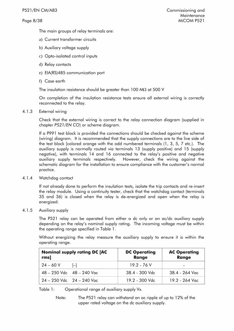
P521/EN CM/A83 Commissioning and Maintenance Page 8/38 MiCOM P521
The main groups of relay terminals are:
a) Current transformer circuits
b) Auxiliary voltage supply
c) Opto-isolated control inputs
d) Relay contacts
e) EIA(RS)485 communication port
f) Case earth
The insulation resistance should be greater than 100 MΩ at 500 V
On completion of the insulation resistance tests ensure all external wiring is correctly reconnected to the relay.
4.1.3 External wiring
Check that the external wiring is correct to the relay connection diagram (supplied in chapter P521/EN CO) or scheme diagram.
If a P991 test block is provided the connections should be checked against the scheme (wiring) diagram. It is recommended that the supply connections are to the live side of the test block [colored orange with the odd numbered terminals (1, 3, 5, 7 etc.). The auxiliary supply is normally routed via terminals 13 (supply positive) and 15 (supply negative), with terminals 14 and 16 connected to the relay’s positive and negative auxiliary supply terminals respectively. However, check the wiring against the schematic diagram for the installation to ensure compliance with the customer’s normal practice.
4.1.4 Watchdog contact
If not already done to perform the insulation tests, isolate the trip contacts and re-insert the relay module. Using a continuity tester, check that the watchdog contact (terminals 35 and 36) is closed when the relay is de-energized and open when the relay is energized.
4.1.5 Auxiliary supply
The P521 relay can be operated from either a dc only or an ac/dc auxiliary supply depending on the relay’s nominal supply rating. The incoming voltage must be within the operating range specified in Table 1.
Without energizing the relay measure the auxiliary supply to ensure it is within the operating range.
Nominal supply rating DC [AC rms]
DC Operating Range
AC Operating Range
24 – 60 V [–] 19.2 - 76 V -
48 – 250 Vdc 48 – 240 Vac 38.4 - 300 Vdc 38.4 - 264 Vac
24 – 250 Vdc 24 – 240 Vac 19.2 - 300 Vdc 19.2 - 264 Vac
Table 1: Operational range of auxiliary supply Vx.
Note: The P521 relay can withstand an ac ripple of up to 12% of the upper rated voltage on the dc auxiliary supply.

Commissioning and P521/EN CM/A83 Maintenance MiCOM P521 Page 9/38
Do not energize the relay or interface unit using the battery charger with the battery disconnected as this can irreparably damage the relay’s power supply circuitry.
Energize the relay only if the auxiliary supply is within the specified operating ranges. If a test block is provided, it may be necessary to link across the front of the test plug to connect the auxiliary supply to the relay.
4.2 With the relay energized
The following group of tests verify that the relay hardware and software is functioning correctly and should be carried out with the auxiliary supply applied to the relay and, if installed, the P590 interface units.
The current transformer connections must remain isolated from the relay for these checks. The trip circuit should also remain isolated to prevent accidental operation of the associated circuit breaker.
4.2.1 Date and time
Before setting the date and time ensure that the factory-fitted battery isolation strip, that prevents battery drain during transportation and storage, has been removed. With the lower access cover open presence of the battery isolation strip can be checked by a red tab protruding from the positive side of the battery compartment. Lightly press on the battery to prevent it from falling out of the battery compartment and pull the red tab to remove the isolation strip.
Set the date and time to the correct local time and date using cells “Date” and “Time” in the PARAMETERS menu.
In the event of the auxiliary supply failing, with a battery fitted in the compartment behind the bottom access cover, the time and date will be maintained. Therefore when the auxiliary supply is restored the time and date will be correct and not need to be set again.
To test this remove the auxiliary supply from the relay for approximately 30 seconds. On re-energization the date and time should be correct.
4.2.2 Light emitting diodes (LEDs)
On power up the green LED should have illuminated and stayed on indicating that the relay is healthy. The relay has non-volatile memory which remembers the state (on or off) of the alarm and trip LEDs when the relay was last energized from an auxiliary supply. Therefore these indicators may also illuminate when the auxiliary supply is applied.
The 8 LED’s, on the front of the relay, can be tested selecting “Yes” in the “LED Test” cell (AUTOMAT. CTRL/Commissioning). The LEDs should remain illuminated for approximately 5 seconds after the LED test is initiated.
4.2.3 Input opto-isolators
This test checks that all the opto-isolated inputs on the relay are functioning correctly. The P521 relay has a total of 5 opto-isolated inputs.
The opto-isolated inputs should be energized one at a time, see external connection diagrams (chapter, P51/EN CO) for terminal numbers. Ensuring correct polarity, connect the auxiliary supply voltage to the appropriate terminals for the input being tested.

P521/EN CM/A83 Commissioning and Maintenance Page 10/38 MiCOM P521
The status of each opto-isolated input can be viewed using the “Input Status” cell, in the OP PARAMETERS menu, a ‘1’ indicating an energized input and a ‘0’ indicating a de-energized input. When each opto-isolated input is energized one of the characters on the bottom line of the display will change to indicate the new state of the inputs.
4.2.4 Output relays
This test checks that all the output relays are functioning correctly. The P521 relay has a total of 8 output relays (not including the watchdog).
Ensure that the commissioning menu is enabled (AUTOMAT. CTRL/Commissioning). The output relays to be tested can be selected in the “Trip Test” cell, 0 = do not close relay and 1 = close relay. Once the output relays have been selected, they can be operated by selecting “yes” in the “Contact Test” cell. The contacts will remain closed until “No” is selected once again.
Note: The contact test will be disabled if “Yes” is selected in the “Disable Relays” cell (also in COMMISSIONING menu).
The output relays should be energized one at a time and the appropriate terminals should be checked with a continuity tester. Operation will be confirmed by the continuity tester operating for a normally open contact and ceasing to operate for a normally closed contact.
Reset the output relays by selecting “No” in the Contact Test” cell.
Note: Ensure that thermal ratings of anything connected to the output relays during the contact test procedure are not exceeded by the associated output relay being operated for too long. It is therefore advised that the time between application and removal of contact test is kept to the minimum.
4.2.5 Rear communications port
This test should only be performed where the relay is to be accessed from a remote location and will vary depending on the communications standard being adopted.
It is not the intention of the test to verify the operation of the complete system from the relay to the remote location, just the relay’s rear communications port and any protocol converter necessary.
Note: The rear communications port must be enabled before access can commence. The port is enabled by selecting “Yes” in the “CTRL Comms” cell (COMMUNICATIONS menu).
EIA(RS)485 connection P521 terminal
Screen 29
+ve 31
–ve 32
Table 2: Rear communications port terminals

Commissioning and P521/EN CM/A83 Maintenance MiCOM P521 Page 11/38
4.2.5.1 MODBUS communications
Connect a portable PC running the appropriate MODBUS Master Station software to the relay’s EIA(RS)485 port via an EIA(RS)485 to EIA(RS)232 interface converter. The terminal numbers for the relay’s EIA(RS)485 port are given in Table 2.
Ensure that the relay address, baud rate, stop bits and parity settings in the application software are set the same as those in cells “Relay Address”, “Baud rate”, “stop bits” and “Parity” (COMMUNICATIONS menu) of the relay.
Check that communications with this relay can be established.
4.2.5.2 IEC 60870-5-103 (VDEW) communications
IEC 60870-5-103/VDEW communication systems are designed to have a local Master Station and this should be used to verify that the relay’s EIA(RS)485 port is working. The terminal numbers for the relay’s EIA(RS)485 port are given in Table 2.
Ensure that the relay address and baud rate settings in the application software are set the same as those in cells “Relay Address” and “Baud rate” (COMMUNICATIONS menu) of the relay.
Check that, using the Master Station, communications with the relay can be established.
4.2.5.3 DNP3.0 communications
Connect a portable PC running appropriate DNP3.0 Master Station software to the relay’s EIA(RS)485 port via an EIA(RS)485 to EIA(RS)232 interface converter. The terminal numbers for the relay’s EIA(RS)485 port are given in Table 2.
Ensure that the relay address, baud rate, stop bits and parity settings in the application software are set the same as those in cells Relay Address”, “Baud rate”, “Stop bits” and “Parity” (COMMUNICATIONS menu) of the relay.
Check that communications with this relay can be established.
4.2.6 Current differential communications
This test verifies that the relay’s current differential EIA(RS)232/EIA(RS)485/fiber optic communications ports and any other peripheral devices (P59x, P595 etc.) used for communications between the P521 current differential relays, at each end of the feeder being protected, are operating correctly.
4.2.6.1 Direct fiber optic communications
Set the “Loopback Test” cell (AUTOMAT. CTRL/Commissioning menu) to “CHANNEL_1” (=ON).
Using a length of fiber optic cable, terminated with an ST connector at each end, connect the transmit (Tx) and receive (Rx) ports on the rear of the relay together. The relay will now respond as if it is connected to a remote relay with the current at the remote end equal to and in phase with the current injected at the local end. Reset any alarm indications and check that no further communications failure alarms are raised. As the loopback alarm is still active it will not reset. Check communication statistics (errored messages etc.) in the “Protection Comms” column (MEASUREMENTS menu).
When connecting or disconnecting optical fibers care should be taken not to look directly into the transmit port or end of the optical fiber.

P521/EN CM/A83 Commissioning and Maintenance Page 12/38 MiCOM P521
Note: since software version V12, the P521 relay provides an “INTERNAL” loopback test facility. By setting the “Loopback Test” cell (AUTOMAT. CTRL/Commissioning menu) to “INTERNAL”, the relay behaviors just as there is a fiber optic linking its Tx and Rx ports.
4.2.6.2 Direct EIA(RS)485 communications
Set the “Loopback Test” cell (AUTOMAT. CTRL/Commissioning menu) to “CHANNEL_1” (=ON).
Using 2 short link wires connect the following:
SK1 terminal 4 to SK1 terminal 6
And
SK1 terminal 5 to SK1 terminal 7
The relay will now respond as if it is connected to a remote relay with the current at the remote end equal to and in phase with the current injected at the local end. Reset any alarm indications and check that no further communications failure alarms are raised. As the loopback alarm is still active it will not reset. Check the communication statistics (e.g. Errored messages etc.) in the “Protection Comms” column (MEASUREMENTS menu).
4.2.6.3 EIA(RS)232 communications
The EIA(RS)232 connections would normally be used to connect the P521 to a modem, or similar device, as a direct link between relays would be practically impossible with EIA(RS)232’s limited transmission distance.
Set the “Loopback Test” cell (AUTOMAT. CTRL/Commissioning menu) to “ON”.
Using a short link wire connect the transmit (SK1 terminal 1) and receive (SK1 terminal 2) ports on the rear of the relay together. The relay will now respond as if it is connected to a remote relay with the current at the remote end equal to and in phase with the current injected at the local end. Reset any alarm indications and check that no further communications failure alarms are raised. As the loopback alarm is still active it will not reset. Check the communication statistics (e.g. Errored messages etc.) in the “Protection Comms” column (MEASUREMENTS menu).
4.2.6.4 Communications using modems
Carefully examine the unit to see that no physical damage has occurred since installation. Check that the external wiring to the modem is correct to the relevant connection diagram or scheme diagram, supplied by the modem manufacturer. Ensure that the modem is being supplied with the correct auxiliary voltage.
Initiate a “Local Analog Loopback” test following the modem user manual.
Return to the P521 relay and select “CHANNEL_1” (=ON) in the “Loopback” cell (AUTOMAT. CTRL/Commissioning). The relay will then respond as if it is connected to a remote relay with the current at the remote end equal to and in phase with the current injected at the local end.
Reset any alarm indications and check that no further communications failure alarms are raised. As the loopback alarm is still active it will not reset. Check channel status, propagation delays and communication statistics in “Protection Comms” column (MEASUREMENTS menu).
Commissioning and P521/EN CM/A83 Maintenance MiCOM P521 Page 13/38
4.2.6.5 Communications using P595 interfacing device
Carefully examine the unit to see that no physical damage has occurred since installation. Check that the external wiring to the P595 is correct to the relevant connection diagram or scheme diagram. Ensure that the applied auxiliary supply voltage corresponds to that stated on the rating label. The rating label is located on the underside of the unit and on the lower side face in front of the terminal strip.
Set the “Loopback Test” cell (AUTOMAT. CTRL/Commissioning menu) to “ON”.
Using 2 short link wires connect the following:
-X9 terminal 4 to –X9 terminal 1
And
-X9 terminal 5 to –X9 terminal 2
The relay will now respond as if it is connected to a remote relay with the current at the remote end equal to and in phase with the current injected at the local end. Reset any alarm indications and check that no further communications failure alarms are raised. As the loopback alarm is still active it will not reset. Check the communication statistics (e.g. Errored messages etc.) in the “Protection Comms” column (MEASUREMENTS menu).
4.2.6.6 Communications using P591 interface units
The P591 converts the optical output of the P521 relay to an electrical signal for a PCM multiplexer with G.703 interfaces. The unit is housed in a size 20TE case and should be located near to the multiplexer.
Before loopback testing can begin some other checks must be completed.
4.2.6.6.1 P591 visual inspection
Carefully examine the unit to see that no physical damage has occurred since installation.
The rating information given under the top access cover on the front of the unit should be checked to ensure it is correct for the particular installation.
Ensure that the case earthing connection, top left-hand corner at the rear of the case, is used to connect the unit to a local earth bar using an adequate conductor.
4.2.6.6.2 P591 insulation
Insulation resistance tests are only necessary during commissioning if it is required for them to be done and they haven’t been performed during installation.
Isolate all wiring from the earth and test the insulation with an electronic or brushless insulation tester at a dc voltage not exceeding 500 V. The auxiliary dc supply terminals should be temporarily connected together.
The insulation resistance should be greater than 100 MΩ at 500 V.
On completion of the insulation resistance tests, ensure all external wiring is correctly reconnected to the P591.
P521/EN CM/A83 Commissioning and Maintenance Page 14/38 MiCOM P521
4.2.6.6.3 P591 external wiring
Check that the external wiring is correct to the relevant connection diagram or scheme diagram. The connection diagram number appears on the rating label under the top access cover on the front of the P591. The corresponding connection diagram will have been supplied with the Schneider Electric T&D order acknowledgement for the P591.
Note: It is especially important that the dc supplies are wired with the correct polarity.
4.2.6.6.4 P591 auxiliary supply
P591 units operate from a dc only auxiliary supply within the operative range of 19 V to 65 V for a 24 – 48 V version and 87.5 V to 300 V for a 110 – 250 V version.
Without energizing the P591 units measure the auxiliary supply to ensure it is within the operating range.
Note: The P591 interface unit is designed to withstand an ac ripple component of up to 12% of the normal dc auxiliary supply. However, in all cases the peak value of the dc supply must not exceed the maximum specified operating limit.
Do not energize the P591 using the battery charger with the battery disconnected as this can irreparably damage the unit’s power supply circuitry.
Energize the P591 only if the auxiliary supply is within the specified operating ranges. If a P991 test block is provided, it may be necessary to link across the front of the test plug to connect the auxiliary supply to the P591.
4.2.6.6.5 P591 light emitting diodes (LEDs)
On power up the green ‘SUPPLY HEALTHY’ LED should illuminate and stay on, thus indicating that the P591 is healthy.
4.2.6.6.6 Loopback test with P591
Remove any external wiring from terminals 3, 4, 7 and 8 at the rear of each P591 unit. Loopback the G.703 signals on each unit by connecting a wire link between terminals 3 and 7, and a second wire between terminals 4 and 8.
Measure and record the optical signal strength received by the P591 by disconnecting the optical fiber from the receive port on the rear of the unit and connecting it to an optical power meter. The mean level should be in the range –16.8 dBm to –25.4 dBm. If the mean level is outside of this range check the size and type of fiber being used.
Measure and record the optical output power of the transmit port of the P591 using the optical power meter and length of 50/125 mm optical fiber. The mean value should be –19.8 dBm ±3 dBm.
Ensure that the transmit (Tx) and receive (Rx) optical fibers between the P521 relay and P591 units are connected.
Return to the P521 relay and select “CHANNEL_1” (=ON) in the “Loopback” cell (AUTOMAT. CTRL/Commissioning). The relay will then respond as if it is connected to a remote relay with the current at the remote end equal to and in phase with the current injected at the local end.
Reset any alarm indications and check that no further communications failure alarms are raised. As the loopback alarm is still active it will not reset. Check channel status, propagation delays and communication statistics in “Protection Comms” column (MEASUREMENTS menu).

Commissioning and P521/EN CM/A83 Maintenance MiCOM P521 Page 15/38
4.2.6.6.7 Final checks
If removed, the secondary front cover should now be re-fitted to the P591.
4.2.6.7 Communications using P592 interface units
The P592 converts the optical output of the P521 relay to an electrical signal for a PCM multiplexer with V.35 interfaces. The unit is housed in a size 20TE case and should be located near to the multiplexer.
Before loopback testing can begin some other checks must be completed.
4.2.6.7.1 P592 visual inspection
Carefully examine the unit to see that no physical damage has occurred since installation.
The rating information given under the top access cover on the front of the unit should be checked to ensure it is correct for the particular installation.
Ensure that the case earthing connection, top left-hand corner at the rear of the case, is used to connect the unit to a local earth bar using an adequate conductor.
4.2.6.7.2 P592 insulation
Insulation resistance tests are only necessary during commissioning if it is required for them to be done and they haven’t been performed during installation.
Isolate all wiring from the earth and test the insulation with an electronic or brushless insulation tester at a dc voltage not exceeding 500 V. The auxiliary dc supply terminals should be temporarily connected together.
Note: The V.35 circuits of the P592 are isolated from all other circuits but are electrically connected to the outer case. The circuits must not therefore be insulation or impulse tested to the case.
The insulation resistance should be greater than 100 MΩ at 500 V.
On completion of the insulation resistance tests ensure all external wiring is correctly reconnected to the P592.
4.2.6.7.3 P592 external wiring
Check that the external wiring is correct to the relevant connection diagram or scheme diagram. The connection diagram number appears on the rating label under the top access cover on the front of the P592. The corresponding connection diagram will have been supplied with the Schneider Electric T&D order acknowledgement for the P592.
Note: It is especially important that the dc supplies are wired with the correct polarity.
4.2.6.7.4 P592 auxiliary supply
P592 units operate from a dc only auxiliary supply within the operative range of 19 V to 300 V.
Without energizing the P592 units measure the auxiliary supply to ensure it is within the operating range.
Note: The P592 interface unit is designed to withstand an ac ripple component of up to 12% of the normal dc auxiliary supply. However, in all cases the peak value of the dc supply must not exceed the maximum specified operating limit.

P521/EN CM/A83 Commissioning and Maintenance Page 16/38 MiCOM P521
Do not energize the P592 using the battery charger with the battery disconnected as this can irreparably damage the unit’s power supply circuitry.
Energize the P592 only if the auxiliary supply is within the specified operating ranges. If a P991 test block is provided, it may be necessary to link across the front of the test plug to connect the auxiliary supply to the P592.
4.2.6.7.5 P592 light emitting diodes (LEDs)
On power up the green ‘SUPPLY HEALTHY’ LED should illuminate and stay on indicating that the P592 is healthy.
The four red LEDs can be tested by appropriate setting of the DIL switches on the unit’s front plate. Set the data rate switch according to the communication channel bandwidth available. Set all other switches to 0. To illuminate the ‘DSR OFF’ and ‘CTS OFF’ LEDs, disconnect the V.35 connector from the rear of the P592 and set the ‘DSR’ and ‘CTS’ switches to ‘0’. The ‘OPTO LOOPBACK’ and ‘V.35 LOOPBACK’ LEDs can be illuminated by setting their corresponding switches to ‘1’.
Once operation of the LEDs has been established set all DIL switches, except for the ‘OPTO LOOPBACK’ switch, to ‘0’ and reconnect the V.35 connector.
4.2.6.7.6 Loopback test
With the ‘OPTO LOOPBACK’ switch in the ‘1’ position the receive and transmit optical ports are electrically connected together. This allows the optical fiber communications between the P521 relay and the P592 to be tested, but not the internal circuitry of the P592 itself.
Measure and record the optical signal strength received by the P592 by disconnecting the optical fiber from the receive port on the rear of the unit and connecting it to an optical power meter. The mean level should be in the range -16.8 dBm to -25.4 dBm. If the mean level is outside of this range check the size and type of fiber being used.
Measure and record the optical output power of the transmit port of the P592 using the optical power meter and length of 50/125 mm optical fiber. The mean value should be –19.8 dBm ±3 dBm.
Ensure that the transmit (Tx) and receive (Rx) optical fibers between the P521 relay and P592 units are connected.
Return to the P521 relay and select “CHANNEL_1” (=ON) in the “Loopback” cell (AUTOMAT. CTRL/Commissioning). The relay will then respond as if it is connected to a remote relay with the current at the remote end equal to and in phase with the current injected at the local end.
Reset any alarm indications and check that no further communications failure alarms are raised. As the loopback alarm is still active it will not reset. Check channel status, propagation delays and communication statistics in “Protection Comms” column (MEASUREMENTS menu).
4.2.6.7.7 Final checksErreur ! Signet non défini.
If removed, the secondary front cover should now be re-fitted to the P592.
4.2.6.8 Communications using P593 interface units
The P593 converts the optical output of the P521 relay to an electrical signal for a PCM multiplexer with X.21 interfaces. The unit is housed in a size 20TE case and should be located near to the multiplexer.
Before loopback testing can begin some other checks must be completed.

Commissioning and P521/EN CM/A83 Maintenance MiCOM P521 Page 17/38
4.2.6.8.1 P593 visual inspection
Carefully examine the unit to see that no physical damage has occurred since installation.
The rating information given under the top access cover on the front of the unit should be checked to ensure it is correct for the particular installation.
Ensure that the case earthing connection, top left-hand corner at the rear of the case, is used to connect the unit to a local earth bar using an adequate conductor.
4.2.6.8.2 P593 insulation
Insulation resistance tests are only necessary during commissioning if it is required for them to be done and they have not been performed during installation.
Isolate all wiring from the earth and test the insulation with an electronic or brushless insulation tester at a dc voltage not exceeding 500 V. The auxiliary dc supply terminals should be temporarily connected together.
Note: The X.21 circuits of the P593 are isolated from all other circuits but are electrically connected to the outer case. The circuits must not therefore be insulation or impulse tested to the case.
The insulation resistance should be greater than 100 MΩ at 500 V.
On completion of the insulation resistance tests ensure all external wiring is correctly reconnected to the P593.
4.2.6.8.3 P593 external wiring
Check that the external wiring is correct to the relevant connection diagram or scheme diagram. The connection diagram number appears on the rating label under the top access cover on the front of the P593. The corresponding connection diagram will have been supplied with the Schneider Electric T&D order acknowledgement for the P593.
Note: It is especially important that the dc supplies are wired with the correct polarity.
4.2.6.8.4 P593 auxiliary supply
P593 units operate from a dc only auxiliary supply within the operative range of 19.5 V to 300 V.
Without energizing the P593 units measure the auxiliary supply to ensure it is within the operating range.
Note: The P593 interface unit is designed to withstand an ac ripple component of up to 12% of the normal dc auxiliary supply. However, in all cases the peak value of the dc supply must not exceed the maximum specified operating limit.
Do not energize the P593 using the battery charger with the battery disconnected as this can irreparably damage the unit’s power supply circuitry.
Energize the P593 only if the auxiliary supply is within the specified operating ranges. If a P991 test block is provided, it may be necessary to link across the front of the test plug to connect the auxiliary supply to the P593.

P521/EN CM/A83 Commissioning and Maintenance Page 18/38 MiCOM P521
4.2.6.8.5 P593 light emitting diodes (LEDs)
On power up the green ‘SUPPLY’ LED should illuminate and stay on indicating that the P593 is healthy.
Set the ‘X.21 LOOPBACK’ switch to ‘ON’. The green ‘CLOCK’ and red ‘X.21 LOOPBACK’ LEDs should illuminate. Reset the ‘X.21 LOOPBACK’ switch to the ‘OFF’ position.
Set the ‘OPTO LOOPBACK’ switch to ‘ON’. The red ‘OPTO LOOPBACK’ LED should illuminate. Do not reset the “OPTO LOOPBACK’ switch as it is required in this position for the next test.
4.2.6.8.6 Loopback test
With the ‘OPTO LOOPBACK’ switch in the ‘ON’ position the receive and transmit optical ports are electrically connected together. This allows the optical fiber communications between the P521 relay and the P593 to be tested, but not the internal circuitry of the P593 itself.
Measure and record the optical signal strength received by the P593 by disconnecting the optical fiber from the receive port on the rear of the unit and connecting it to an optical power meter. The mean level should in the range –16.8 dBm to –25.4 dBm. If the mean level is outside of this range check the size and type of fiber being used.
Measure and record the optical output power of the transmit port of the P593 using the optical power meter and length of 50/125 mm optical fiber. The mean value should be –19.8 dBm ±3 dBm.
Ensure that the transmit (Tx) and receive (Rx) optical fibers between the P521 relay and P593 units are connected.
Set the ‘OPTO LOOPBACK’ and ‘X.21 LOOPBACK’ switch to ‘OFF’ and ‘ON’ respectively. With the ‘X.21 LOOPBACK’ switch in this position the ‘Receive Data’ and ‘Transmit Data’ lines of the X.21 communication interface are connected together. This allows the optical fiber communications between the P521 relay and the P593, and the internal circuitry of the P593 itself to be tested.
Return to the P521 relay and select “CHANNEL_1” (=ON) in the “Loopback” cell (AUTOMAT. CTRL/Commissioning). The relay will then respond as if it is connected to a remote relay with the current at the remote end equal to and in phase with the current injected at the local end.
Reset any alarm indications and check that no further communications failure alarms are raised. As the loopback alarm is still active it will not reset. Check channel status, propagation delays and communication statistics in “Protection Comms” column (MEASUREMENTS menu).
4.2.6.8.7 Final checks
If removed, the secondary front cover should now be re-fitted to the P593.
4.2.7 Current inputs
This test verifies that the accuracy of current measurement is within the acceptable tolerances.
All relays will leave the factory set for operation at a system frequency of 50 Hz. If operation at 60 Hz is required then this must be set in the “Frequency” cell in the OP PARAMETERS menu.

Commissioning and P521/EN CM/A83 Maintenance MiCOM P521 Page 19/38
Apply current equal to the line current transformer secondary winding rating to each current transformer input of the corresponding rating in turn, see table 1 or external connection diagram, see chapter P521/EN CO for appropriate terminal numbers, checking its magnitude using a multimeter. The corresponding reading can then be checked in the MEASUREMENTS/Current/General column and value displayed recorded.
Note: Some of the relay protection elements may operate during this test, depending upon the relay setting.
CT Rating (Amps) Terminals
1 A 49 and 50
1 B 51 and 52
1 C 53 and 54
1 N 55 and 56
5 A 41 and 42
5 B 43 and 44
5 C 45 and 46
5 N 47 and 48
Table 3: Current input connections
The measured current values displayed on the relay LCD, or a portable PC connected to the front communication port, will be in primary amperes, providing the CT ratio has been set. The values displayed should be equal to the applied current multiplied by the corresponding current transformer ratio set in the “CT Ratio” column (CONFIGURATION menu).
The measurement accuracy of the relay is typically ±0.2% at rated current. However, an additional allowance must be made for the accuracy of the test equipment being used.

P521/EN CM/A83 Commissioning and Maintenance Page 20/38 MiCOM P521
5. SETTING CHECKS
The setting checks ensure that all of the application-specific relay settings (i.e. both the relay’s function and programmable scheme logic settings), for the particular installation, have been correctly applied to the relay.
If the application-specific settings are not available, ignore sections 5.1 and 5.2.
Note: The trip circuit should remain isolated during these checks to prevent accidental operation of the associated circuit breaker.
For additional security the P521 output contacts can be disabled using the commissioning menu. For more information on this feature refer to section 3.5.4.1 of the User Guide, see chapter P521/EN FT.
5.1 Apply application-specific settings
There are two methods of applying the settings to the relay:
− Transferring them from a pre-prepared setting file to the relay using a portable PC running the appropriate software via the relay’s front EIA(RS)232 port, located under the bottom access cover, or rear EIA(RS)485/K Bus communications port. This method is preferred for transferring function settings as it is much faster and there is less margin for error.
− If a setting file has been created for the particular application and provided on a diskette this will further reduce the commissioning time.
− Enter them manually via the relay’s user interface.
5.2 Demonstrate correct relay operation
Test 4.2.7 has already demonstrated that the relay is within calibration, therefore the purpose of these tests are as follows:
− To determine that the primary protection function of the relay, current differential, can trip according to the correct application settings.
− To verify correct setting of any backup phase overcurrent protection.
− To verify correct assignment of the trip contacts, by monitoring the response to a selection of fault injections.
5.2.1 Current differential bias characteristic
To avoid spurious operation of any overcurrent, earth fault, negative sequence overcurrent, thermal overload, broken conductor, under current or breaker fail elements these should be disabled for the duration of the differential element tests. Refer to the User Guide for information on how this can be done. Make a note of which elements need to be re-enabled after testing. The relay should also be set to loopback mode isolating it from the remote end. Refer to section 4.2.6.1.

Commissioning and P521/EN CM/A83 Maintenance MiCOM P521 Page 21/38
5.2.1.1 Connect the test circuit
The following tests require a variable auto transformer (variac) and two resistors connected as shown in Figure 1. Alternatively an injection test set can be used to supply Ιa and Ιb.
Figure 1: Connection for bias characteristic testing
A current is injected into the A phase which is used as the bias current and another current is injected into the B phase which is used as differential current. Ιa is always greater than Ιb.
5.2.1.2 Lower slope
Make sure that the relay is in loopback mode as described in 4.2.6.1.
Adjust the variac and the resistor to give a bias current of 1 pu in the A-phase.
Note: 1 pu = 1 A into terminals 49-50 for 1 A applications; or 1 pu = 5 A into terminals 41-42 for 5 A applications). The relay will trip and any contacts associated with the current differential protection will operate, this will be accompanied by the “I DIFF” and “I DIFF I-TRIP” alarms. Some LEDs may illuminate and the yellow alarm LED will start to flash. Acknowledge the alarm by pressing the key followed by key. The yellow LED will stop flashing and become continuously illuminated.
Operation of the A Phase element will be indicated by an “A” appearing in the “IDiff Trip Flags” cell, (AUTOMAT. CTRL/Commissioning) as shown below.
IDiff Trip Flags
TRIP: A
This indication will remain until the A-Phase differential current exits the tripping region of the biased differential characteristic.
When the current in the A Phase is established, close the switch and slowly increase the current in the B phase from zero until Phase B trips. This will be indicated by a “B” appearing in the “IDiff Trip Flags” menu, in addition to “A” that is already indicated, as shown below.
IDiff Trip Flags
TRIP: A B
P521/EN CM/A83 Commissioning and Maintenance Page 22/38 MiCOM P521
Record the phase B current magnitude and check that it corresponds to the formula below.
Switch OFF the ac supply, read and clear all alarms.
The formula below can be used to calculate the B phase operate current (enter slope ‘k1’ in pu form, i.e. percentage/100).
B phase operate current = 0.5 x (Ιs1 + k1) pu +/- 10%
5.2.1.3 Upper slope
Repeat the test in 5.2.1.2 with the bias current set in the A-phase to be 3 pu.
When the current in A Phase is established, close the switch and slowly increase the current in the B phase from zero until phase B trips. Record the phase B current magnitude and check that it corresponds to the information below.
Switch OFF the ac supply and reset the alarms.
The formula below can be used to calculate the B phase operate current (enter slope ‘k1’ in pu form, i.e. percentage/100).
B Phase operate current = 0.5 x [(3 x k2) – (k2 – k1) x Ιs2 + Ιs1] pu +/- 20%
Note: For 5 A applications the duration of current injections should be short to avoid overheating of the variac, resistors or injection test set.
5.2.2 Current differential operating time
Retaining the same test circuit as before, prepare for an instantaneous injection of 3 pu current in the A phase with no current in the B phase (B phase switch open). Connect a timer to start when the fault injection is applied and to stop when the trip occurs. The operating time of the relay should be recorded. Repeat the test for phases B and C, reconfiguring the test equipment accordingly.
The average of the recorded operating times for the three phases should be less than the values shown in table 4. Switch OFF the ac supply and reset the alarms.
Baud rate (Protection Comms) Maximum Operating Times
9.6 kb/s 100 ms
19.2 kb/s 80 ms
56 kb/s 45 ms
64 kb/s 45 ms
Table 4: P521 Instantaneous operating times
Note: Where an IDMT or DMT delay is set, in the PROTECTION G1 /[87] Current Diff menu column, the expected operating time is typically within +/- 5% of that for the curve equation plus the “instantaneous” delay quoted above.
On completion of the tests any overcurrent, earth fault, negative sequence overcurrent, thermal overload, broken conductor, under current or breaker fail elements which were disabled for testing purposes must have their original settings restored in the appropriate menu columns.
Commissioning and P521/EN CM/A83 Maintenance MiCOM P521 Page 23/38
5.2.3 Backup phase overcurrent protection
If the overcurrent protection function is being used, the Ι> element should be tested. If not, skip to section 5.3
To avoid spurious operation of any other protection functions, such as current differential, breaker fail etc. these should be disabled for the duration of the overcurrent tests. Make a note of which elements need to be re-enabled after testing.
Note: If the Ι> element is set to be enabled on “Backup” only (i.e. when the protection communications fail), it will be necessary to deliberately force a communications channel failure in order to test it. This can be achieved by removing the loopback test, and ensuring that the relay cannot communicate with the remote end relay.
− Set “Loopback” cell (AUTOMAT. CTRL /Commissioning) to “OFF”
− Observe that the relay raises a COMMS FAIL alarm. This may take up to 10 seconds depending upon the setting of the “Comms Fail Timer” (COMMUNICATIONS menu).
5.2.3.1 Connect the test circuit
Determine which output relay has been selected to operate when an Ι> trip occurs by viewing the “tI>” cell in the AUTOMAT. CTRL/Output Relays menu.
The associated terminal numbers can be found in the external connection diagram (chapter P521/EN CO).
Connect the output relay so that its operation will trip the test set and stop the timer.
Connect the current output of the test set to the ‘A’ phase current input of the relay (terminals 49 and 50 where 1 A current transformers are being used and terminals 41 and 42 for 5 A current transformers).
Ensure that the timer will start when the current is applied to the relay.
5.2.3.2 Perform the test
Ensure that the timer is reset.
Apply a current of twice the setting in “I>” cell (PROTECTION G1/[50/51] Phase OC) to the relay and note the time displayed when the timer stops.
Check that the red trip LED has illuminated.
5.2.3.3 Check the operating time
Check that the operating time recorded by the timer is within the range shown in Table 5.
Note: Except for the definite time characteristic, the operating times given in Table 5 are for a time multiplier or time dial setting of 1. Therefore, to obtain the operating time at other time multiplier or time dial settings, the time given in Table 5 must be multiplied by the appropriate TMS or TD setting.
In addition, for definite time and inverse characteristics there is an additional delay of up to 0.02 second and 0.08 second respectively that may need to be added to the relay’s acceptable range of operating times.

P521/EN CM/A83 Commissioning and Maintenance Page 24/38 MiCOM P521
For all characteristics allowance must be made for the accuracy of the test equipment being used.
Characteristic Operating Time at Twice Current Setting and
Time Multiplier/Time Dial Setting of 1.0
Nominal (Seconds) Range (Seconds)
DMT tΙ>1 setting Setting ±2%
IEC STI (Short Time Inverse) 1.78 1.60 – 1.96
IEC SI (Standard Inverse) 10.03 9.00 – 11.0
IEC VI (Very Inverse) 13.50 12.2 – 14.5
IEC EI (Extremely Inverse) 26.67 24.0 – 29.3
UK LTI (Long Time Inverse) 120.00 108 – 132
CO2 (Short Time Inverse) 1.73 1.56 – 1.90
IEEE MI (Moderately Inverse) 3.80 3.42 – 4.18
CO8 (Inverse) 2.16 1.94 – 2.38
IEEE VI (Very Inverse) 7.03 6.33 – 7.73
IEEE EI (Extremely Inverse) 9.52 8.57 – 10.5
RI 4.52 4.07 – 4.97
Table 5: Characteristic operating times for Ι>
On completion of the tests any current differential, negative sequence overcurrent, thermal overload, broken conductor, under current or breaker fail elements which were disabled for testing purposes must have their original settings restored in the appropriate menu columns.
5.3 Check application settings
The settings applied should be carefully checked against the required application-specific settings to ensure that they are correct, and have not been mistakenly altered during the injection test.
There are two methods of checking the settings:
− Extract the settings from the relay using a portable PC running the appropriate software via the front EIA(RS)232 port, located under the bottom access cover, or rear communications port (with an appropriate protocol converter connected). Compare the settings transferred from the relay with the original written application-specific setting record. (For cases where the customer has only provided a printed copy of the required settings but a portable PC is available).
− Step through the settings using the relays user interface and compare them with the original application-specific setting record.

Commissioning and P521/EN CM/A83 Maintenance MiCOM P521 Page 25/38
6. END TO END TESTS
In section 4.2.6 a loopback test was initiated on the relay fiber optic communications channels, together with the P59x/modem interface units, if installed, to verify correct operation of the communications channel local to the P521 relay whilst completing the remaining tests. In this test the loopback is removed and, if possible, satisfactory communications between P521 relays in the same group will be confirmed.
Note: The trip circuit should remain isolated during these checks to prevent accidental operation of the associated circuit breaker.
6.1 Remove the loopback test
As well as removing the loopback, this section checks that all wiring and optical fibers/pilots are reconnected. If modems, P592 or P593 interface units are installed the application-specific settings will also be applied.
Check the relay alarms to ensure that no communications failure alarms have occurred whilst the loopback test has been in progress.
Set cell the Loopback cell to ‘OFF’.
Restore the communications channels as per the appropriate sub-section below.
6.1.1 Direct fiber optic communications
Remove the loopback test fiber and reconnect the fiber optic cables for communications between relays, ensuring correct placement.
When connecting or disconnecting optical fibers care should be taken not to look directly into the transmit port or end of the optical fiber.
6.1.2 Direct EIA(RS)485 communications
Remove the 2 short link wires between SK1 terminals 4 and 6 and SK1 terminals 5 and 7.
Ensure that all external wiring that has been removed to facilitate testing is replaced in accordance with the relevant connection diagram or scheme diagram.
6.1.3 EIA(RS)232 communications
Remove the short link wire between SK1 terminals 1 and 2.
Ensure that all external wiring that has been removed to facilitate testing is replaced in accordance with the relevant connection diagram or scheme diagram.
6.1.3.1 Communications using modems
Remove “Local Analog Loopback” test following the modem user manual.
6.1.3.2 Communications using P595 interfacing device
Remove the short link wires between –X9 terminals 1 and 4 and –X9 terminals 2 and 5.
Ensure that all external wiring that has been removed to facilitate testing is replaced in accordance with the relevant connection diagram or scheme diagram.
If isolation transformers are not used between long communications wires, these should be handled as pilot wire circuits to avoid the risk of electric shock.
P521/EN CM/A83 Commissioning and Maintenance Page 26/38 MiCOM P521
6.1.4 Communications using P591 interface units
Return to the P591 units.
Ensure that all external wiring that has been removed to facilitate testing is replaced in accordance with the relevant connection diagram or scheme diagram.
If applicable, replace the secondary front cover on the P591 units.
6.1.5 Communications using P592 interface units
Return to the P592 units.
Ensure that all external wiring that has been removed to facilitate testing is replaced in accordance with the relevant connection diagram or scheme diagram.
Set the ‘V.35 LOOPBACK’ switch to the ‘0’ position.
Set the ‘CLOCK SWITCH’, ‘DSR’, ‘CTS’ and ‘DATA RATE’ DIL switches on each unit to the positions required for the specific application and ensure the ‘OPTO LOOPBACK’ switch is in the ‘0’ position.
If applicable, replace the secondary front cover on the P592 units.
Note: V.35 Loopback on the remote P592 can be selected to check the communications between the local relay, the local P592 and the communication link itself.
6.1.6 Communications using P593 interface units
Return to the P593 units.
Ensure that all external wiring that has been removed to facilitate testing is replaced in accordance with the relevant connection diagram or scheme diagram.
Set the ‘X.21 LOOPBACK’ switch to the ‘OFF’ position and ensure the ‘OPTO LOOPBACK’ switch is also in the ‘OFF’ position.
If applicable, replace the secondary front cover on the P593 units.
Note: X.21 Loopback on the remote P593 can be selected to check the communications between the local relay, the local P593 and the X.21 communication link itself. This setting on the local P593 can also be used to check the communications between the local relay and the local P593 if required.
6.2 Verify communications between relays
Check for correct communications between relays as per the appropriate sub-section below.
6.2.1 Communication checks for direct fiber or P59x connected relays
The following communication checks confirm that the optical power at the transmit and receive ports of the local relay are within the recommended operating limits. However, these checks can only be performed with the relays (and P59x interface units if installed) at the other end of the feeder known to be functional and energized.
Measure and record the optical signal strength received by the local P521 relay by disconnecting the optical fiber from the Channel 1 receive port and connecting it to an optical power meter. The mean level should be in the range –16.8 dBm to -25.4 dBm for an 850 nm port. For relays delivered from December 2008 (optical fiber interface card marked with “43 dB”), the mean level should be in the range -6 dBm to -49 dBm for a 1300 nm port. For relays delivered pre-December 2008, the mean level should
Commissioning and P521/EN CM/A83 Maintenance MiCOM P521 Page 27/38
be in the range –7 dBm to – 37 dBm for a 1300 nm port. If the mean level is outside of this range check the size and type of fiber being used.
When connecting or disconnecting optical fibers care should be taken not to look directly into the transmit port or end of the optical fiber.
Measure and record the optical power of the Channel 1 transmit port using the optical power meter and length of optical fiber. The mean value should be in the range - 16.8 dBm to -22.8 dBm for an 850 nm port. For relays delivered from December 2008 (optical fiber interface card marked with “43 dB”), the mean level should be in the range -3 dBm to -9 dBm for a 1300 nm port. For relays delivered pre-December 2008, the mean level should be in the range -7 dBm to -13 dBm for a 1300 nm port.
Ensure that all transmit (Tx) and receive (Rx) optical fibers are reconnected to the P521, ensuring correct placement.
Reset any alarm indications and check that no further communications failure alarms are raised. Check that the number of valid messages is increasing and that the number of errored messages stops increasing. These cells can be found in the MEASUREMENTS/Protection Comms column.
To reset the protection comms statistics, press in the “Comms Stats RST” cell.
6.2.2 Communication checks for metallic communications (direct EIA(RS)485, P595, EIA(RS)232 and modem connected relays)
If isolation transformers are not used between long communications wires, these should be handled as pilot wire circuits to avoid the risk of electric shock.
Ensure that all transmit (Tx) and receive (Rx) leads are reconnected to the P521.
Note: For EIA(RS)232 communications it must be ensured that the SK1 terminal 3 is also connected. Failure to do this may result in unreliable communications.
Reset any alarm indications and check that no further communications failure alarms are raised. Check that the number of valid messages is increasing and that the number of errored messages stops increasing. These cells can be found in the MEASUREMENTS/Protection Comms column.
The protection comms statistics can be reset, if necessary, by pressing in the “Comms Stats RST” cell.
7. ON-LOAD CHECKS
The objectives of the on-load checks are to:
− Confirm the external wiring to the current inputs is correct.
− Measure the magnitude of capacitive current.
− Ensure the on-load differential current is well below the relay setting.
− Check the polarity of the line current transformers at each end is consistent.
However, these checks can only be carried out if there are no restrictions preventing the energization of the plant being protected and the other P521 relays in the group have been commissioned.

P521/EN CM/A83 Commissioning and Maintenance Page 28/38 MiCOM P521
Remove all test leads, temporary shorting leads, etc. and replace any external wiring that has been removed to allow testing.
If it has been necessary to disconnect any of the external wiring from the relay in order to perform any of the foregoing tests, it should be ensured that all connections are replaced in accordance with the relevant external connection or scheme diagram.
7.1 Confirm current transformer wiring
Measure the current transformer secondary values for each input using a multimeter connected in series with the corresponding relay current input.
Ensure the current flowing in the neutral circuit of the current transformers is negligible.
Compare the values of the secondary phase currents with the relay’s measured values, which can be found in the MEASUREMENTS/Current/General menu column.
Note: Under normal load conditions the earth fault function will measure little, if any, current. It is therefore necessary to simulate a phase to neutral fault. This can be achieved by temporarily disconnecting one or two of the line current transformer connections to the relay and shorting the terminals of these current transformer secondary windings. However, if a single dedicated current transformer is used for the earth fault function, it is not possible to check the relay’s measured values.
If no CT ratio has been entered (CONFIGURATION/CT Ratios) the currents displayed on the LCD or a portable PC connected to the front EIA(RS)232 communication port of the relay should be equal to the applied secondary current. The values should be within 1% of the applied secondary currents. However, an additional allowance must be made for the accuracy of the test equipment being used.
If a CT ratio has been entered the currents displayed on the relay should be equal to the applied secondary current multiplied by the corresponding current transformer ratio. Again the values should be within 1% of the expected value, plus an additional allowance for the accuracy of the test equipment being used.
7.2 Measure capacitive charging current
With the feeder energized from one end only, compare the local and remote measured currents in the MEASUREMENTS/Current Diff menu column to confirm that the feeder capacitive charging current is similar to that expected on all three phases.
Check that the Ιs1 setting is higher than 2.5 times the capacitive charging current. If this is not the case notify the Engineer who determined the original settings of the setting required to ensure stability under normal operating conditions.
7.3 Check differential current
With the feeder supplying load current check that the relay measurements in the “Current/General” menu column are as expected and that the differential current is similar to the value of the capacitive charging current previously measured for all three phases.

Commissioning and P521/EN CM/A83 Maintenance MiCOM P521 Page 29/38
7.4 Check consistency of current transformer polarity
The load current should be high enough to be certain beyond doubt that the main current transformers are connected with the same polarity to each relay in the group.
There is a possibility on cable circuits with high line capacitance that the load current could be masked by the capacitive charging current. If necessary reverse the connections to the main current transformers and check that the ‘A’ phase differential current in cell “Differential IA” (MEASUREMENTS/Current Diff) is significantly higher than for the normal connection. If the differential current falls with the connection reversed the main current transformers may not be correct and should be thoroughly checked. Repeat the test for phases ‘B’ and ‘C’ using the “Differential IB” and “Differential IC” cells respectively.
8. FINAL CHECKS
The tests are now complete.
Remove all test or temporary shorting leads, etc. If you have disconnected any of the external wiring from the relay in order to perform the wiring verification tests, make sure all connections are replaced in accordance with the relevant external connection or scheme diagram.
If the relay is in a new installation, or the circuit breaker has just been maintained, the circuit breaker maintenance and current counters should be zero. These counters can be reset using the “CB Operation RST” and “ΣAmps (n) RST” cells in the (RECORD/CB Monitoring).
If a P991/MMLG test block is installed, remove the P992/MMLB test plug and replace the cover so that the protection is put into service.
Ensure that all event records, fault records, disturbance records, alarms and LEDs have been reset before leaving the relay.
9. MAINTENANCE
9.1 Maintenance period
It is recommended that products supplied by Schneider Electric T&D receive periodic monitoring after installation. As with all products some deterioration with time is inevitable. In view of the critical nature of protective relays, and their infrequent operation, it is desirable to confirm that they are operating correctly at regular intervals.
Schneider Electric T&D protective relays are designed for a life in excess of 20 years.
MiCOM P521 current differential relay is self-supervising and so requires less maintenance than earlier designs of relay. Most problems will result in an alarm so that remedial action can be taken. However, some periodic tests should be done to ensure that the relay is functioning correctly and the external wiring is intact.
The operation of the P59x interface units, when installed, is continuously monitored by the P521 relay and a communication failure alarm will therefore be given if a P59x should cease to work properly.

P521/EN CM/A83 Commissioning and Maintenance Page 30/38 MiCOM P521
Note: A communication failure alarm could be caused by the failure of the equipment forming the communication link and can not in itself be conclusive evidence of a faulty P59x interface unit.
If a Preventative Maintenance Policy exists within the customer’s organization then the recommended product checks should be included in the regular programme. Maintenance periods will depend on many factors, such as:
− Operating environment
− Accessibility of the site
− Amount of available manpower
− Importance of the installation in the power system
− Consequences of failure
9.2 Maintenance checks
Although some functionality checks can be performed from a remote location by utilizing the communications ability of the relays, these are predominantly restricted to checking that the relay is measuring the applied currents and voltages accurately, and checking the circuit breaker maintenance counters. Therefore it is recommended that maintenance checks are performed locally (i.e. at the substation itself).
Before carrying out any work on the equipment, the user should be familiar with the contents of the Safety and Technical Data chapters and the ratings on the equipment’s rating label.
9.2.1 Alarms
The alarm status LED should first be checked to identify if any alarm conditions exist. If so, press the read key [ ] repeatedly to step through the alarms.
Clear the alarms to extinguish the LED.
9.2.2 Opto-isolators
The opto-isolated inputs can be checked to ensure that the relay responds to their energization by repeating the commissioning test detailed in section 4.2.3 of this Commissioning and Maintenance Guide.
9.2.3 Output relays
The output relays can be checked to ensure that they operate by repeating the commissioning test detailed in section 4.2.4 of this Commissioning and Maintenance Guide.
9.2.4 Measurement accuracy
If the power system is energized, the values measured by the relay can be compared with known system values to check that they are in the approximate range that is expected. If they are then the analog/digital conversion and calculations are being performed correctly by the relay. Suitable test methods can be found in section 7.1 of this Commissioning and Maintenance Guide.
Alternatively, the values measured by the relay can be checked against known values injected into the relay via the test block, if fitted, or injected directly into the relay terminals. A suitable test method can be found in section 4.2.7 of this Commissioning and Maintenance Guide. These tests will prove the calibration accuracy is being maintained.

Commissioning and P521/EN CM/A83 Maintenance MiCOM P521 Page 31/38
9.3 Equipment failure
Before carrying out any work on the equipment, the user should be familiar with the content of the Safety and Technical Data chapters and the ratings on the equipment’s rating label.
The MiCOM P521 relay is fully digital and performs constant self-diagnosis. Any failure of software or hardware elements is instantly detected. As soon as an internal fault is detected, depending on its type (minor or major), an alarm message is displayed as a priority on the front panel LCD before the fault LED is illuminated (fixed or flashing) and the watchdog relay is closed (if the fault is a major one).
An equipment failure (major or minor) cannot be acknowledged on the front panel (using the dedicated tactile button keypad). Only the disappearance of the cause will acknowledge the fault and hence reset the fault LED.
9.3.1 Minor fault
A control communications failure would be regarded as a minor fault by the P521. If the control communications are faulty, the protection and automation modules are not affected.
Message:
"COMM.ERROR": Control communication faulty
Cause:
Hardware or software failure of the control communications module.
Action:
Withdraw the active part and return it to the factory for repair.
Alternative: If the control communication is not used, disable communication in the COMMUNICATION/ CTRL Comms menu (CTRL Comms? = No).
Message:
“RAM ERROR” : Battery backed RAM faulty
“BATTERY FAIL”: Battery faulty or flat.
Cause:
See section 9.4.3 of this Commissioning and Maintenance Guide. If the message still remains after restart return the module to the factory for repair.

P521/EN CM/A83 Commissioning and Maintenance Page 32/38 MiCOM P521
9.3.2 Protection comms fault
As soon as a problem with the protection comms is detected the operation of the main protection is stopped. All other protection elements continue to operate and those selected as backup in the current setting group will be enabled.
Message:
“COMMS ALARM CH1”: communications channel failure detected.
Cause:
Hardware or software failure of the communications card.
Hardware failure of the communications module retained in the case when the active part is withdrawn.
Failure of the relay at the distant end of the communications link.
Failure of a device in the communications path or break in the communications link.
Live parts exposed within the P521 case, when the P521 module is removed.
Action:
Determine the location of the failure using the P520L loopback test box (see Accessories section).
Initiate a loopback test on the back of each of the relays. If the protection comms alarm resets then the fault is with the communications link not the relays. The relays should assist with diagnosing the location of the fault by indicating the faulty path (Tx, Rx or both). If the protection comms alarm does not reset on one relay it is likely that the relay is faulty.
To diagnose if the fault is in the active (removal) part of the relay or the protection communications card, remove the relay and plug in the P520L loopback test box as shown in Figure 2. It is recommended that the battery is tested, before inserting the test box, by selecting battery test and checking that the green LED illuminates. With the loopback tester inserted select “Loopback Test” using the selector switch and ensure that the green LED illuminates. Initiate a loopback test from the remote relay so that the comms signal passes through the local relay communications card. If the comms fail alarm on the remote relay disappears, then the protection comms card is functioning correctly, hence the problem is with only the active part. If the comms fail alarm does not reset then the local protection comms card is faulty.

Commissioning and P521/EN CM/A83 Maintenance MiCOM P521 Page 33/38
! "
#$ % &'#(
& )*+
Figure 2: Application of P520L loopback test box
If the fault is with the active part of the relay, withdraw the active part and return it to the factory for repair.
If the fault is with the communications module the whole relay, including the case, must be returned to the factory for repair.
If the fault is in any other part of the system the relays will automatically resume communication as soon as the link is restored.
9.3.3 Major fault
Major faults for the MiCOM P521 relay are all software and hardware failures, except the communication faults. As soon as this type of failure is detected the watchdog (WD) is closed and all operations are stopped (protection, automation, communication).
9.3.3.1 Hardware and software faults
Messages:
"SETTING ERROR": Data zone in fault
"EEPROM ERROR CALIBR.": Calibration data faulty
"CT ERROR": Analog channel faulty
“DEFAULT SETTING” : Default settings restored
“PROT COMMS FAIL” : Protection Comms card faulty
Cause:
Hardware or software failure.
Action:
Restart the protection software by interrupting the auxiliary supply for approximately ten seconds. In the case of the “DEFAULT SETTING” and “SETTING ERROR” alarms the in-service settings should be re-applied. If the software fault still remains after restart withdraw the active part and return the module to the factory for repair.

P521/EN CM/A83 Commissioning and Maintenance Page 34/38 MiCOM P521
9.4 Method of repair
9.4.1 Replacing the active part
The case and the rear terminals blocks have been designed to facilitate removal of the MiCOM P521 relay without disconnecting the scheme wiring, should replacement or repair become necessary.
Note: The MiCOM range of relays have integral current transformer shorting switches which will close when the active part is removed from the case.
Remove the upper and lower flap without exerting excessive force. Remove the external screws. Under the upper flap, turn the extractor with a 3mm screwdriver and extract the active part of the relay by pulling from the upper and lower notches on the front panel of the MiCOM relay.
Then reinstall the repaired or replacement relay following the above instruction in reverse, ensuring that no modification has been made to the scheme wiring.
Note: The rear protection communications interface is designed to be retained inside the case to avoid disconnection of the communications.
9.4.2 Replacing the complete relay
To remove the complete relay (active part and case) the entire wiring must be removed from the rear connector.
Before working at the rear of the relay isolate all current supplies to the MiCOM relay and ensure that the relay is no longer energized.
DANGER: NEVER OPEN THE SECONDARY CIRCUIT OF A CURRENT TRANSFORMER SINCE THE HIGH VOLTAGE PRODUCED MAY BE LETHAL AND COULD DAMAGE INSULATION.
Remove all wiring (communication, logic inputs, outputs, auxiliary voltage, current inputs). Disconnect the relay earth connection from the rear of the relay.
If isolation transformers are not used between long communications wires, these should be handled as pilot wire circuits to avoid the risk of electric shock.
Remove the screws used to fasten the relay to the panel, rack, etc. These are the screws with the larger diameter heads that are accessible when the upper and lower flaps are installed.
Withdraw the relay from the panel, rack, etc. taking care because it will be heavy due to the internal transformers.
To reinstall the repaired or replacement relay follow the above instructions in reverse, ensuring that each terminal block is relocated in the correct position and the case earth and communications are replaced.
Once reinstallation is complete the relay should be re-commissioned using the instruction in sections 1 to 8 of this Commissioning and Maintenance Guide.
Commissioning and P521/EN CM/A83 Maintenance MiCOM P521 Page 35/38
9.4.3 Changing the battery
The MiCOM P521 has a battery to maintain recorded data and the correct time when the auxiliary voltage fails. The data maintained include event, fault and disturbance records and the thermal state at the time of supply failure.
The battery is designed for a life of 10 years in standard atmospheric conditions.
"Battery backed RAM memory" message could be the result of a battery failure.
"Battery Fail" message is the result of a battery failure.
To replace the battery follow the following instructions.
• Open the lower flap on the front of the relay
• Gently extract the battery from its socket. If necessary, use a small screwdriver.
• Ensure that metal terminals in the battery socket are free from corrosion, grease and dust.
• The replacement battery should be removed from its packaging and placed into the battery holder, ensure that the polarity markings on the battery agree with those adjacent to the socket.
Note: Only use a type 1/2 AA lithium battery with a nominal voltage of 3.6 V.
• Ensure that the battery is securely held in its socket and that the battery terminals are making good contact with the metal terminals of the socket.
• Close the lower flap on the front of the relay.
• The battery that has been removed should be disposed of in accordance with the disposal procedure for Lithium batteries in the country in which the relay is installed.
9.4.4 Extracting the rear communications board from the relay
• Remove the two screws from under the top access panel on the front interface, followed by the two screws from under the bottom access panel.
• Utilizing the extractor cams located under the top and bottom access panels, extract the relay from the casing.
• Remove the 4 mounting screws at the rear of the case that are situated around the communications mounting plate.
• Pull the plate through to the front of the case taking care not to cause damage to the inside of the casing and the communications card.
• Insert the new communications card by carefully pushing the card from the front to the rear of the casing.
• Re-fit the 4 screws to securely hold the communications mounting plate in position.
• Reset the extractor cams to the normal flush state and insert the relay into the case, taking care to align the relay with the communications card connector.
• Re-fit the two screws under the top access panel on the front interface, followed by the two screws under the bottom access panel.

P521/EN CM/A83 Commissioning and Maintenance Page 36/38 MiCOM P521
Note: It is strongly recommended that the tests contained within sections 4.2.6 of this section be repeated once the communications interface has been changed.
!"#$
%#"
%##"
Figure 3: Screw locations (front view)
$$, *
--
Figure 4: Screw locations (back view)

Commissioning and P521/EN CM/A83 Maintenance MiCOM P521 Page 37/38
9.5 Problem solving
9.5.1 Password lost or not accepted
Problem:
Password lost or not accepted
Cause:
The MiCOM P521 relay is supplied with the password set to AAAA. This password can be changed by the user (refer to OP PARAMETERS menu in the User Guide of this manual).
Action:
There is an additional unique recovery password associated with the relay which can be supplied by the factory or service agent, if given details of its serial number (under the upper flap of the front panel). With this serial number, contact your Schneider Electric T&D local dealer or Schneider Electric T&D, After Sales Dept.
9.5.2 Communication
9.5.2.1 Values measured locally and remotely
Problem:
The measurements noted remotely and locally (via EIA(RS)485 communication) differ.
Cause:
The values accessible on the front face via the Measurement menu are refreshed every second. Those fed back via the communication and accessible by the Schneider Electric T&D setting software generally have variable refreshing frequencies. If the refreshing frequency of the supervision software differs from that of MiCOM P521 relay (1 s), there may be a difference between indicated values.
Action:
Adjust the frequency for refreshing the measurements of the supervision software or of the setting software to 1 second.
9.5.2.2 MiCOM relay no longer responds
Problem:
No response from MiCOM P521 relay when asked by the supervision software without any communication fault message.
Cause:
Mainly, this type of problem is linked to an error in the MiCOM P521 communication parameters.
Action:
Check MiCOM P521 communication parameters (data rate, parity, etc.) are in accordance with the supervision settings.
Check MiCOM P521 network address.
Check that this address is not used by another device connected on the same LAN.
Check that the other devices on the same LAN answer to supervision requests.

P521/EN CM/A83 Commissioning and Maintenance Page 38/38 MiCOM P521
9.5.2.3 A remote command is not taken into account
Problem:
The communication between the relay and the PC is correct, but the relay does not accept any remote command or file downloading.
Cause:
Generally this is due to the fact that the relay is in a programming situation. This means that the password is active (password by on key pad).
Action:
Check that the password has not been set in the relay within the last 5 minutes.

Connection Diagrams P521/EN CO/C63 MiCOM P521
CONNECTION DIAGRAMS
Date: 1st December 2009
Software version: 10
Connection diagram: 10P52101

P521/EN CO/C63 Connection Diagrams MiCOM P521

Connection Diagrams P521/EN CO/C63 MiCOM P521 Page 1/12
Figure 1: External connections - with fiber optic communications

P521/EN CO/C63 Connection Diagrams Page 2/12 MiCOM P521
Figure 2: External connections - with direct EIA(RS)485 communications
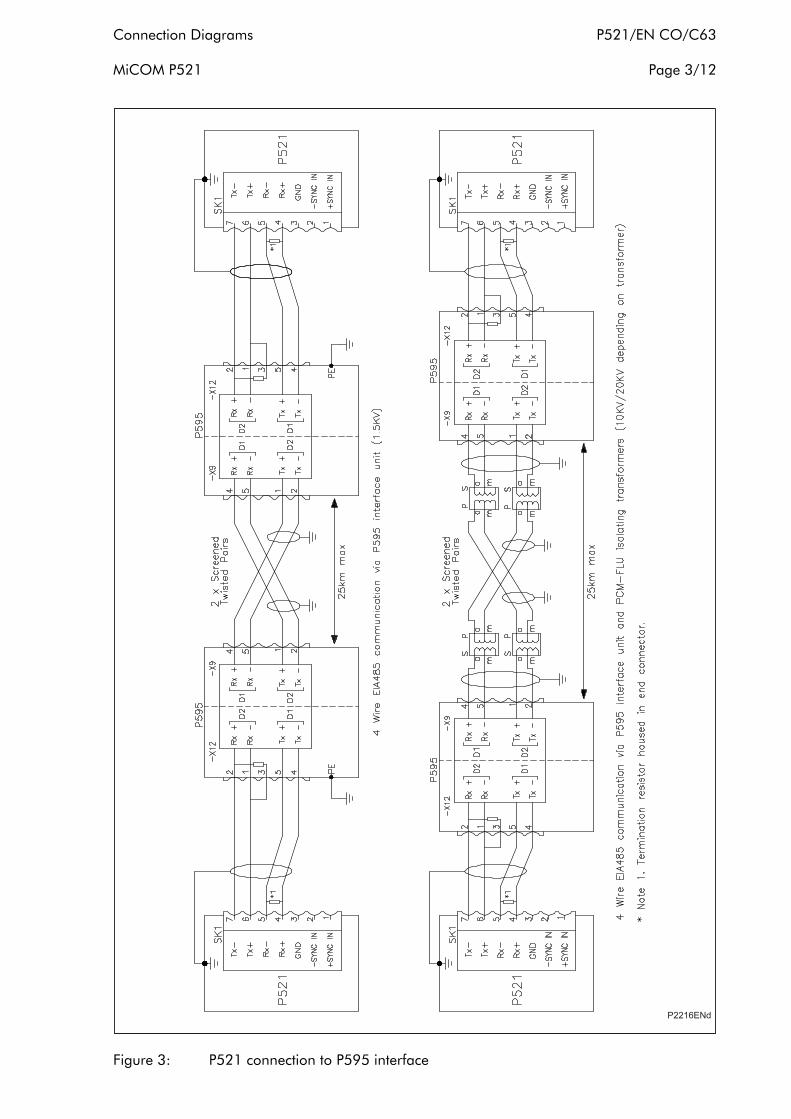
Connection Diagrams P521/EN CO/C63 MiCOM P521 Page 3/12
Figure 3: P521 connection to P595 interface

P521/EN CO/C63 Connection Diagrams Page 4/12 MiCOM P521
Figure 4: P521 connection to baseband 1092A and mDSL 1095 modems (see also Figure 6)

Connection Diagrams P521/EN CO/C63 MiCOM P521 Page 5/12
Figure 5: P521 connection to Westermo TD36B modem (see also Figure 6)

P521/EN CO/C63 Connection Diagrams Page 6/12 MiCOM P521
Figure 6: Line connection diagrams
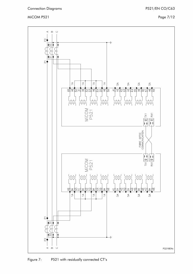
Connection Diagrams P521/EN CO/C63 MiCOM P521 Page 7/12
Figure 7: P521 with residually connected CT’s

P521/EN CO/C63 Connection Diagrams Page 8/12 MiCOM P521
Figure 8: P521 with core balanced CT’s

Connection Diagrams P521/EN CO/C63 MiCOM P521 Page 9/12
Figure 9: P521 with DY11 in zone transformer

P521/EN CO/C63 Connection Diagrams Page 10/12 MiCOM P521
Figure 10: External connections - with EIA(RS)232 communications

Connection Diagrams P521/EN CO/C63 MiCOM P521 Page 11/12
Figure 11: P521 connection to Keymile Line Runner DTM modem

P521/EN CO/C63 Connection Diagrams Page 12/12 MiCOM P521
Modem Configuration P521/EN MC/A83 MiCOM P521
MODEM CONFIGURATION
Date: 1st October 2010
Software version: 12
Connection diagram: 10P52101

P521/EN MC/A83 Modem Configuration MiCOM P521

Modem Configuration P521/EN MC/A83 MiCOM P521 Page 1/16
CONTENTS
1. INTRODUCTION 3
2. DEFINITIONS 3
3. LEASED LINE MODEM WESTERMO TD32 4 3.1 DIP switch set “S1” 4 3.1.1 Operating modes 4 3.2 DIP switch set “S2” 4 3.2.1 DCE to DTE communication types 4 3.3 DIP switch set “S3” 5 3.3.1 DCE to DCE communication hardware 5 3.4 DIP switch set “S4” 6 3.5 DIP switch set “S5” 7 3.5.1 Control line pull-up 7 3.6 Line requirements 7 3.7 Propagation delay 7
4. TD-36 MODEM 8
5. “NETLINK” 1095 MDSL MODEM 9 5.1 DIP switch set “S2” 9 5.2 DIP switch set “S3” 10 5.3 Line requirements 10 5.4 Propagation delay 10
6. 2 WIRE “CAMPUS” 1092A DRIVER MODEM 11 6.1 DIP switch set “S1” 11 6.2 DIP switch set “S2” 11 6.3 Line requirements 12 6.4 Relay settings for 2 wire 1092A modem 12 6.5 Propagation delay 12
7. 4 WIRE “CAMPUS” 1092A DRIVER MODEM 13 7.1 DIP switch set “S1” 13 7.2 DIP switch set “S2” 13 7.3 Line requirements 14 7.4 Relay settings for 4 wire 1092A modem 14 7.5 Propagation delay 14

P521/EN MC/A83 Modem Configuration Page 2/16 MiCOM P521
8. LINERUNNER DTM MODEM WITH V36 INTERFACE 15 8.1 Connection between relay and modem 15 8.2 Setting of modem 15
9. P595 16 9.1 Propagation delay 16
10. WIRE PARAMETERS 16
FIGURES
Figure 1: Standard dial up 4 Figure 2: Asynchronous comms DTR/DSR disconnected 5 Figure 3: Flow control off – 2 or 4 wire 5 Figure 4: Typical TD-32 line connections - 1 6 Figure 5: 9.6 kbits/s Direct mode data bits no parity 6 Figure 6: V.32 bis 9.6 kbits/s line modulation 7 Figure 7: Using the top connector block RTS to DSR and DCS to DTR 7 Figure 8: Clock configuration 10 Figure 9: DTE rate of 64 kbits/s 10 Figure 10: Modem setting switches 12 Figure 11: Modem setting switches 14

Modem Configuration P521/EN MC/A83 MiCOM P521 Page 3/16
1. INTRODUCTION
This chapter outlines the basic setting up procedure for leased line, baseband ‘campus’ and ‘NetLink’ mDSL modems, and P595 device. Although the setting up procedure is specific to these modems it is hoped that the setting principle could be used as a guide for modems of a similar design.
2. DEFINITIONS
Unconditioned pilot wires:
Twisted pair of metallic wire between 19 (0.9 mm) and 26 AWG (0.4 mm). Standard dial-up telephone circuits, leased circuits that run through signal equalization equipment or standard flat modular telephone cable are not acceptable.
Conditioned leased lines:
Leased circuits that run through signal equalization equipment using the standard flat modular telephone cable.
Modem: Generic name for a converter of digital data to a format suitable for transmission over unconditioned pilot wires or conditioned leased lines.
Baud: The number of data symbols transmitted every second.
DCE: Data Communication Equipment i.e. modems, protocol converters and line drivers.
DTE: Data Terminal Equipment i.e. PCs, terminals and protection relays.
Handshaking: Confirmation and status signals sent between communicating devices in order to check the data stream. There are two general types, hardware (RTS/CTS) and software (XON/XOFF).
TD: Transmitted data. Data going from DTE to DCE.
RD: Received data. Data going from DCE to DTE.
RTS: Ready To Send. Hardware handshake generated by the DTE to determine if the DCE is ready to receive data. Expected response is from the CTS line.
CTS: Clear To Send. Hardware handshake generated by the DCE in response to a RTS signal.
DSR: Data Set Ready. A signal from the DCE used to indicate that it is powered and useable.
DTR: Data Terminal Ready. A signal from the DTE showing it is powered and ready.
DCD: Data Carrier Detect. A signal from the DCE showing that a carrier is present and the line is ready for data transmission.
Switch shown in ON position.

P521/EN MC/A83 Modem Configuration Page 4/16 MiCOM P521
3. LEASED LINE MODEM WESTERMO TD32
The simplest way to set the modem is to use the DIP switch sets. There are five DIP switch sets in total and each sets a different aspect of the modem operation.
Non defined switches are to be set to the off position.
3.1 DIP switch set “S1”
S1 sets the operating mode of the modem.
3.1.1 Operating modes
There are three modem operating modes to choose from. These are:
1. Dial up
2. Leased line answering
3. Leased line originating
For a leased line one modem must be in originate mode (mode 3) to initiate communication and the other in answer mode (mode 2) to wait for communication to be initialized by the originate modem. On standard telephone networks (i.e. conditioned leased lines) both modems should be set to dial-up mode. See switch settings below:
Figure 1: Standard dial up
3.2 DIP switch set “S2”
S2 sets the type of communication between the DCE and the DTE. In this case the modem is the DCE and the MICOM P521 is the DTE.
3.2.1 DCE to DTE communication types
There is a choice of 5 communication types. These are:
1. Asynchronous
2. Synchronous using the clock from the P521
3. Synchronous using a clock generated from the local modem
4. Synchronous using a clock recovered from the local modem via the line
5. DTR/DSR disconnected
The P521 electrical protection communications port conforms to 3 wire EIA(RS)232 or 4 wire EIA(RS)485. Consequently the modem should be set as asynchronous with DTR/DSR disconnected.

Modem Configuration P521/EN MC/A83 MiCOM P521 Page 5/16
!"#$%"$
Figure 2: Asynchronous comms DTR/DSR disconnected
3.3 DIP switch set “S3”
S3 is the setting switch that indicates the type of line being used between the modems.
3.3.1 DCE to DCE communication hardware
Three line type options are available. These are:
1. 4 wire connection
2. 2 wire connection
3. Flow control
The choice between 4 and 2 wire connection depends on whether one or two twisted pairs of conductors are available for use between the modems.
For all P521 applications no flow control is required, so the flow control should always be turned off. Flow control provides handshaking between the DCE and the DTE, but this also requires additional signal lines on top of the usual 2 or 4.
&'((
Figure 3: Flow control off – 2 or 4 wire
&'((

P521/EN MC/A83 Modem Configuration Page 6/16 MiCOM P521
)
)*
)
)*
Figure 4: Typical TD-32 line connections - 1
3.4 DIP switch set “S4”
S4 sets the serial speed (input to modem) and format of the data between the modem and the relay.
For optimum performance the TD32 modem should be set at 9.6 kbits/s in direct mode 8 data bits, 1 stop bit and no parity (see switch setting below). Higher baud rates may be available on other modems, however, it is essential that the data rate is common throughout the communications link; i.e. the relay data rate must be the same as the serial speed of the modem and the line modulation (output from modem).
+!,-%" -
(
Figure 5: 9.6 kbits/s Direct mode data bits no parity
Modem Configuration P521/EN MC/A83 MiCOM P521 Page 7/16
3.5 DIP switch set “S5”
S5 sets the line modulation (output from modem) used between the modems.
For optimum performance the TD32 modem should be set to V.32 bis 9.6 kbits/s.
.!-+!,-%
Figure 6: V.32 bis 9.6 kbits/s line modulation
3.5.1 Control line pull-up
Since the modem will not be making use of the control lines they need to be forced high so they are permanently enabled. This is done by connecting RTS to DSR and DCD to DTR using the connector block at the top of the modem.
+
$ #" $" $# /# "/" "# $ " $ 0
1 1 1 1 1 + 1 1 1
Figure 7: Using the top connector block RTS to DSR and DCS to DTR
3.6 Line requirements
The maximum transmission distance depends on the attenuation of the line. The maximum value of attenuation is 30 dBm. To have a good error rate it is recommended to keep the attenuation under 20 dBm which is approximately 20 km.
3.7 Propagation delay
Typical propagation delay = 24.3 ms.

P521/EN MC/A83 Modem Configuration Page 8/16 MiCOM P521
4. TD-36 MODEM
The TD-32 modem has gone obsolete and is replaced by TD-36 modem. The setting of DIP switches of TD-36 are shown in the table below.
Calling Modem Answering Modem
DIP Switch Switch Position
Setting Description DIP Switch Switch Position
Setting Description
S1 1 On S1 1 On
2 On 2 On
3 On 3 On
4 Off
19.2 K
4 Off
19.2 K
5 On 5 On
6 On 6 On
7 Off 7 Off
8 Off
8N 1S
8 Off
8N 1S
S2 1 On S2 1 Off
2 On
Leased Line Calling
2 On
Leased Line Answering
3 Off RS232 3 Off RS232
4 On RS-422/485 4W 4 On RS-422/485 4W
5 On 4 Wire Leased Line 5 On 4 Wire Leased Line
6 Off Back Up of Leased Line Disabled
6 Off Back Up of Leased Line Disabled
7 Off PSTN Answering 7 Off PSTN Answering
8 Off Use Stored Values 8 Off Use Stored Values
S3 1 Off Use Stored Values S3 1 Off Use Stored Values
2 Off Use Stored Values 2 Off Use Stored Values
3 On 3 On
4 Off
Reliable Mode Enabled
4 Off
Reliable Mode Enabled
5 Off Use Stored Values 5 Off Use Stored Values
6 Off Use Stored Values 6 Off Use Stored Values
7 On 7 On
8 Off
Termination Receiver in 4 Wire Mode
8 Off
Termination Receiver in 4 Wire Mode
S4 1 Off Use Stored Values S4 1 Off Use Stored Values
2 Off Use Stored Values 2 Off Use Stored Values
3 On Data Compression Disabled
3 On Data Compression Disabled
4 Off Use Stored Values 4 Off Use Stored Values

Modem Configuration P521/EN MC/A83 MiCOM P521 Page 9/16
Calling Modem Answering Modem
DIP Switch Switch Position
Setting Description DIP Switch Switch Position
Setting Description
5 On 5 On
6 On 6 On
7 On 7 On
8 On
Automatic Line Speed
8 On
Automatic Line Speed
S5 1 On S5 1 On
2 On 2 On
3 Off 3 Off
4 Off
Termination of R in 4 Wire
4 Off
Termination of R in 4 Wire
5. “NETLINK” 1095 MDSL MODEM
The simplest way to set the modem is to use the DIP switch sets. There are three DIP switch sets in total but only DIP switch sets S2 and S3 need to be set, as all of the switches on DIP switch set S1 are reserved for future use and are to be set to the On position.
For DIP switch set S3, non defined switches are to be set to the off position.
5.1 DIP switch set “S2”
S2-6 and S2-7 control the clock configuration for the data transmission. One modem must be set as Originating, with Internal clock mode (transmit clock generated internally), and the other modem must be set as Receive, with Receive Recover clock mode (clock recovered from the received data).
Clock Mode Description S2-6 S2-7
Internal Transmit clock generated internally
On On
External Transmit clock derived from the P521
Off On
Receive Recover Transmit clock derived from the line
On Off
Disabled Reserved Off Off

P521/EN MC/A83 Modem Configuration Page 10/16 MiCOM P521
Example:
)2# 32( (
End A - Originating End B - Receive
Figure 8: Clock configuration
5.2 DIP switch set “S3”
S3 controls the data rate between the modem and the P521. The most appropriate rate for this is 64 kbits/s. All other data rates are unsuitable for the P521.
"#4(3-%
Figure 9: DTE rate of 64 kbits/s
5.3 Line requirements
Transmission Distance
No Cross Talk
DTE Rates 26 AWG (0.4
mm) 24 AWG (0.5
mm) Link Rate (kbps)
km km
144 64 6.6 9.4
5.4 Propagation delay
Typical propagation delay = 2.3 ms.
)23

Modem Configuration P521/EN MC/A83 MiCOM P521 Page 11/16
6. 2 WIRE “CAMPUS” 1092A DRIVER MODEM
The simplest way to set the modem is to use the DIP switch sets. There are 2 DIP switch sets in total.
Non defined switches are to be set to the off position.
6.1 DIP switch set “S1”
S1-1 and S1-2 control the data rate between the modem and the P521. The most appropriate rate for this is 64 kbits/s.
Sync Data Rate S1-1 S1-2
56 kbps Off On
64 kbps On Off
S1-6 and S1-7 control the clock configuration for the data transmission. One modem must be set as Originating, with Internal clock mode (transmit clock generated internally), and the other modem must be set as Receive, with Receive Recover clock mode (clock recovered from the received data).
Clock Mode Description S1-6 S1-7
Internal Transmit clock generated internally
On On
External Transmit clock derived from the P521
Off On
Receive Recover Transmit clock derived from the line
On Off
Disabled Reserved Off Off
6.2 DIP switch set “S2”
S2-4 selects either 2-wire or 4-wire operation. For 2-wire operation, it should be set Off.
S2-6 allows remote loopback tests to be performed
P521/EN MC/A83 Modem Configuration Page 12/16 MiCOM P521
End A - Originating (Internal clock mode)
End B - Receive (Receive recover clock mode)
Figure 10: Modem setting switches
6.3 Line requirements
Wire Gauge Wire Diameter Distance
19 AWG 0.9 mm 17.2 km
22 AWG 0.64 mm 11.5 km
24 AWG 0.5 mm 8 km
26 AWG 0.4 mm 5.5 km
6.4 Relay settings for 2 wire 1092A modem
Relay Setting Value
Protocol NRZ
Data Rate 64 K (as recommended above)
Clock Source CH1 External
6.5 Propagation delay
Typical propagation delay = 1.02 ms.
Modem Configuration P521/EN MC/A83 MiCOM P521 Page 13/16
7. 4 WIRE “CAMPUS” 1092A DRIVER MODEM
The simplest way to set the modem is to use the DIP switch sets. There are 2 DIP switch sets in total.
Non defined switches are to be set to the off position.
7.1 DIP switch set “S1”
S1-1 and S1-2 control the data rate between the modem and the P521. The most appropriate rate for this is 64kbits/s.
Sync Data Rate S1-1 S1-2
56 kbps Off On
64 kbps On Off
S1-6 and S1-7 control the clock configuration for the data transmission. One modem must be set as Originating, with Internal clock mode (transmit clock generated internally), and the other modem must be set as Receive, with Receive Recover clock mode (clock recovered from the received data).
Clock Mode Description S1-6 S1-7
Internal Transmit clock generated internally
On On
External Transmit clock derived from the P521
Off On
Receive Recover Transmit clock derived from the line
On Off
Disabled Reserved Off Off
7.2 DIP switch set “S2”
S2-4 selects either 2-wire or 4-wire operation. For 4-wire operation, it should be set On.
S2-6 allows remote loopback tests to be performed
P521/EN MC/A83 Modem Configuration Page 14/16 MiCOM P521
End A - Originating (Internal clock mode)
End B - Receive (Receive recover clock mode)
Figure 11: Modem setting switches
7.3 Line requirements
Wire Gauge Wire Diameter Distance
19 AWG 0.9 mm 18.2 km
22 AWG 0.64 mm 12.1 km
24 AWG 0.5 mm 8.5 km
26 AWG 0.4 mm 5.7 km
7.4 Relay settings for 4 wire 1092A modem
Relay Setting Value
Protocol NRZ
Data Rate 64 K (as recommended above)
Clock Source CH1 External
7.5 Propagation delay
Typical propagation delay = 1.02 ms.

Modem Configuration P521/EN MC/A83 MiCOM P521 Page 15/16
8. LINERUNNER DTM MODEM WITH V36 INTERFACE
The “Campus” 1092A modem from Patton has gone obsolete and is replaced by LineRunner DTM modem with V36 interface from Keymile. The EIA(RS)485 communication interface of P521 relay should be chosen to work with this modem.
8.1 Connection between relay and modem
The connection between P521 and modem is listed below:
P521: Phoenix Contact KGG-MC 1,5/7 Connector
DTM Modem: V.36 (37 Way Male D-type) Connector
Pin 7 : TX - Pin 22 : Send Data -
Pin 6 : TX + Pin 4 : Send Data +
Pin 5 : RX - Pin 24 : Receive Data -
Pin 4 : RX + Pin 6 : Receive Data +
Pin 2: Receive Clock - Pin 26 : Receive Timing -
Pin 1: Receive Clock + Pin 8 : Receive Timing +
Note: All other pins not specified above are not connected.
8.2 Setting of modem
The modems come with setting software ASMOS on a CD. The following settings need changing from the default to make them work.
Local Modem Setting:
User Interface -> General Tab -> User Interface Mode : V.36 Sub Bit Rates
User Interface -> General Tab -> XV Interface : Port Enabled
User Interface -> V.36 Config Tab ->User Data Rate : 1x 64Kbit/s
User Interface -> V.36 Config Tab ->Clock Mode : Intern
User Interface -> V.36 Config Tab ->Edge Select : Rising
User Interface -> V.36 Config Tab ->Sub rate Configuration -> Mode (Sub Rate Transmission) : Off (Synchronous)
User Interface -> V.36 Config Tab ->Control Flow -> Request to send : Forced to 1
User Interface -> V.36 Config Tab ->Control Flow -> Data Set Ready : Forced to 1
User Interface -> V.36 Config Tab ->Control Flow -> Data Channel Recieved : Forced to 1
Line Interface -> General Tab-> Port Pair Mode : 1 Pair
Line Interface -> General Tab-> Span Config ->Min Line Rate: 32x64 K +8 K
Line Interface -> General Tab-> Span Config ->Max Line Rate: 32x64 K +8 K

P521/EN MC/A83 Modem Configuration Page 16/16 MiCOM P521
Remote Modem Settings:
User Interface -> General Tab -> User Interface Mode : V.36 Sub Bit Rates
User Interface -> General Tab -> XV Interface : Port Enabled
User Interface -> V.36 Config Tab ->Edge Select : Rising
User Interface -> V.36 Config Tab ->Control Flow -> Request to send : Forced to 1
User Interface -> V.36 Config Tab ->Control Flow -> Data Set Ready : Forced to 1
User Interface -> V.36 Config Tab ->Control Flow -> Data Channel Recieved : Forced to 1
9. P595
See separate P595 manual (P595/EN M).
9.1 Propagation delay
Typical propagation delay = 1.08 ms.
10. WIRE PARAMETERS
Wire Gauge Capacitance Resistance
19 AWG 51.5 nF/km 53.45 Ω/km
22 AWG 51.5 nF/km 106.96 Ω/km
24 AWG 51.5 nF/km 169.46 Ω/km
26 AWG 51.5 nF/km 273.86 Ω/km

Accessories P521/EN AC/A83 MiCOM P521
ACCESSORIES
Date: 1st October 2010
Software version: 12
Connection diagram: 10P52101

P521/EN AC/A83 Accessories MiCOM P521

Accessories P521/EN AC/A83 MiCOM P521 Page 1/8
CONTENTS
1. INTRODUCTION 3
2. ACCESSORIES ORDER CODES 3
3. MT-RS485 SURGE PROTECTION DEVICE 4
3.1 Interface details 4
3.1.1 Transmission rate 4
3.1.2 Transmission method 4
3.1.3 Nominal discharge current 4
3.1.4 Output voltage limiting 4
3.1.5 Response time 4
3.2 Environmental conditions 4
3.2.1 Temperature range 4
3.2.2 Enclosure protection 4
3.3 Mounting and connection 4
3.3.1 Weight 4
3.3.2 Case design 4
3.3.3 Case dimensions 5
3.3.4 Installation position 5
3.3.5 Terminations 5
4. PCM-FLU 10 KV OR 20 KV ISOLATING TRANSFORMERS 5
4.1 General data 5
4.2 Connection diagrams 6
5. P520L LOOPBACK TEST BOX 7
5.1 Function of loopback test box 7
5.2 General data 8
5.3 Battery data 8
5.4 Circuit diagram 8

P521/EN AC/A83 Accessories Page 2/8 MiCOM P521
FIGURES
Figure 1: PCM-FLÜ isolating transformer 20 kV 6 Figure 2: PCM-FLÜ isolating transformer 10 kV 6 Figure 3: Application of P520L loopback test box 7 Figure 4: Circuit diagram for P520L loopback test box 8
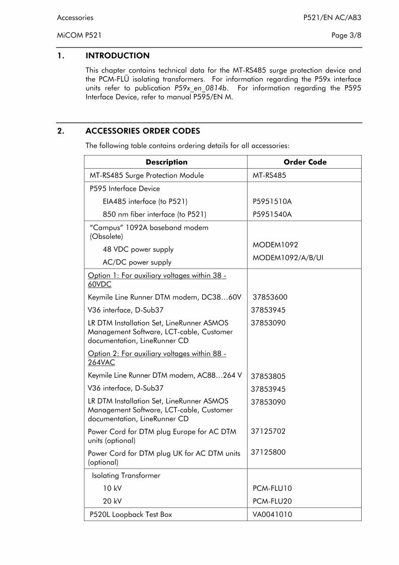
Accessories P521/EN AC/A83 MiCOM P521 Page 3/8
1. INTRODUCTION
This chapter contains technical data for the MT-RS485 surge protection device and the PCM-FLÜ isolating transformers. For information regarding the P59x interface units refer to publication P59x_en_0814b. For information regarding the P595 Interface Device, refer to manual P595/EN M.
2. ACCESSORIES ORDER CODES
The following table contains ordering details for all accessories:
Description Order Code
MT-RS485 Surge Protection Module MT-RS485
P595 Interface Device
EIA485 interface (to P521)
850 nm fiber interface (to P521)
P5951510A
P5951540A
“Campus” 1092A baseband modem (Obsolete)
48 VDC power supply
AC/DC power supply
MODEM1092
MODEM1092/A/B/UI
Option 1: For auxiliary voltages within 38 - 60VDC
Keymile Line Runner DTM modem, DC38…60V
V36 interface, D-Sub37
LR DTM Installation Set, LineRunner ASMOS Management Software, LCT-cable, Customer documentation, LineRunner CD
Option 2: For auxiliary voltages within 88 - 264VAC
Keymile Line Runner DTM modem, AC88…264 V
V36 interface, D-Sub37
LR DTM Installation Set, LineRunner ASMOS Management Software, LCT-cable, Customer documentation, LineRunner CD
Power Cord for DTM plug Europe for AC DTM units (optional)
Power Cord for DTM plug UK for AC DTM units (optional)
37853600
37853945
37853090
37853805
37853945
37853090
37125702
37125800
Isolating Transformer
10 kV
20 kV
PCM-FLU10
PCM-FLU20
P520L Loopback Test Box VA0041010

P521/EN AC/A83 Accessories Page 4/8 MiCOM P521
Description Order Code
Interface card of P521 (for spare/upgrade)
EIA232
EIA485
850 nm multi-mode fiber
1300 nm multi-mode fiber
1300 nm single-mode fiber
GN0230002
GN0230010
GN0230004
GN0230006
GN0230008
Note: The P595 Interface Device is identical to the Schneider Electric T&D PZ511 interface except that the P595 has accessible setting switches. The switch settings are detailed in the P595 Interface Device manual, P595/EN M.
3. MT-RS485 SURGE PROTECTION DEVICE
3.1 Interface details
3.1.1 Transmission rate
Maximum baud rate of 64 kbps.
3.1.2 Transmission method
Half or full duplex.
3.1.3 Nominal discharge current
Ιd,nom (8/20 µs) : 10 kA.
3.1.4 Output voltage limiting
At 1kV/µs : <22 V (sym./asym. [GND]).
<650 V (asym. [PE]).
3.1.5 Response time
tr : <1 ns (sym./asym. [GND]).
<100 ns (asym. [PE]).
3.2 Environmental conditions
3.2.1 Temperature range
Operating Temperature : -20°C to +60°C or -4°F to 140°F.
3.2.2 Enclosure protection
IP20 according to DIN VDE 0470 and EN 60529 or IEC 529.
3.3 Mounting and connection
3.3.1 Weight
Approximately 150g.
3.3.2 Case design
Suitable for installation on a top-hat rail per DIN EN 50022.
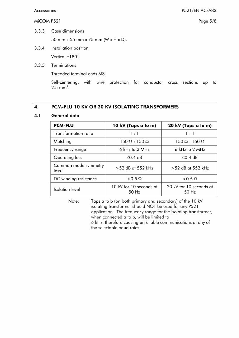
Accessories P521/EN AC/A83 MiCOM P521 Page 5/8
3.3.3 Case dimensions
50 mm x 55 mm x 75 mm (W x H x D).
3.3.4 Installation position
Vertical ±180°.
3.3.5 Terminations
Threaded terminal ends M3.
Self-centering, with wire protection for conductor cross sections up to 2.5 mm2.
4. PCM-FLU 10 KV OR 20 KV ISOLATING TRANSFORMERS
4.1 General data
PCM-FLU 10 kV (Taps a to m) 20 kV (Taps a to m)
Transformation ratio 1 : 1 1 : 1
Matching 150 Ω : 150 Ω 150 Ω : 150 Ω
Frequency range 6 kHz to 2 MHz 6 kHz to 2 MHz
Operating loss ≤0.4 dB ≤0.4 dB
Common mode symmetry loss
>52 dB at 552 kHz >52 dB at 552 kHz
DC winding resistance <0.5 Ω <0.5 Ω
Isolation level 10 kV for 10 seconds at
50 Hz 20 kV for 10 seconds at
50 Hz
Note: Taps a to b (on both primary and secondary) of the 10 kV isolating transformer should NOT be used for any P521 application. The frequency range for the isolating transformer, when connected a to b, will be limited to 6 kHz, therefore causing unreliable communications at any of the selectable baud rates.

P521/EN AC/A83 Accessories Page 6/8 MiCOM P521
4.2 Connection diagrams
Figure 1: PCM-FLÜ isolating transformer 20 kV
Figure 2: PCM-FLÜ isolating transformer 10 kV
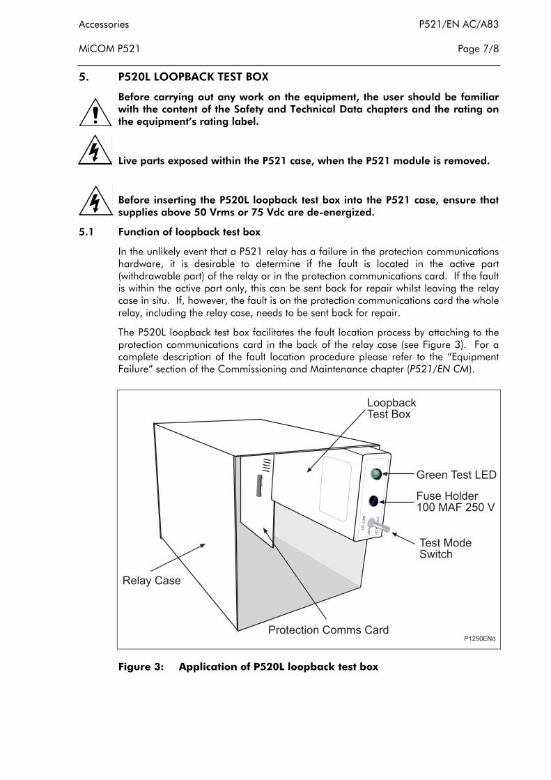
Accessories P521/EN AC/A83 MiCOM P521 Page 7/8
5. P520L LOOPBACK TEST BOX
Before carrying out any work on the equipment, the user should be familiar with the content of the Safety and Technical Data chapters and the rating on the equipment’s rating label.
Live parts exposed within the P521 case, when the P521 module is removed.
Before inserting the P520L loopback test box into the P521 case, ensure that supplies above 50 Vrms or 75 Vdc are de-energized.
5.1 Function of loopback test box
In the unlikely event that a P521 relay has a failure in the protection communications hardware, it is desirable to determine if the fault is located in the active part (withdrawable part) of the relay or in the protection communications card. If the fault is within the active part only, this can be sent back for repair whilst leaving the relay case in situ. If, however, the fault is on the protection communications card the whole relay, including the relay case, needs to be sent back for repair.
The P520L loopback test box facilitates the fault location process by attaching to the protection communications card in the back of the relay case (see Figure 3). For a complete description of the fault location procedure please refer to the “Equipment Failure” section of the Commissioning and Maintenance chapter (P521/EN CM).
!"#
$%
&'( )
(*+
Figure 3: Application of P520L loopback test box

P521/EN AC/A83 Accessories Page 8/8 MiCOM P521
5.2 General data
The P520L loopback test box has a 3 position switch:
• BATTERY TEST
• OFF
• LOOPBACK TEST
Selecting the “BATTERY TEST” momentary position will illuminate the green LED if the battery is healthy. It is recommended that the battery is checked before a loopback test is performed.
The “LOOPBACK TEST” option should be selected once the test box is securely attached to the protection communications card. The LED should illuminate if the test box is correctly fitted.
The “OFF” position should be selected during storage of the loopback test box in order to prevent unnecessary battery drain.
5.3 Battery data
A PP3 (9 V) battery must be used to power the P520L loopback test box.
5.4 Circuit diagram
,-
)..&
,/01
& )
-)2 )&
"
%
!"
3+3& &!*++.! "
-)
4
,
5
-
/
6
4
,
5
7
)
33
Figure 4: Circuit diagram for P520L loopback test box

Commissioning Test and P521/EN RS/A83 Record Sheets MiCOM P521
COMMISSIONING TEST AND RECORD SHEETS
Date: 1st October 2010
Software version: 12
Connection diagram: 10P52101

P521/EN RS/A83 Commissioning Test and Record Sheets MiCOM P521

Commissioning Test and P521/EN RS/A83 Record Sheets MiCOM P521 Page 1/34
CONTENTS
1. COMMISSIONING TEST RECORD 3
2. SETTING RECORD 13
2.1 OP Parameters 13
2.2 Configuration 13
2.2.1 Display 13
2.2.2 CT ratios 14
2.2.3 LED 14
2.2.4 Group select 15
2.2.5 Alarms 15
2.2.6 Configuration inputs 16
2.2.7 Phase rotation 16
2.3 Communication 16
2.3.1 Ctrl comms (MODBUS protocol) 16
2.3.2 Ctrl comms (IEC 60870-5-103 protocol) 16
2.3.3 Ctrl comms (DNP3.0) 16
2.3.4 Protection 17
2.4 Protection G1/G2 17
2.4.1 [87] Current diff 17
2.4.2 [50/51] Phase O/C 18
2.4.3 [50N/51N] E/Gnd 18
2.4.4 [46] Neg seq OC 19
2.4.5 [49] Therm OL 20
2.4.6 [37] Undercurrent 20
2.5 Automat. ctrl 20
2.5.1 Trip commands 20
2.5.2 Latch functions 21
2.5.3 Blocking logic 1/2 22
2.5.4 Logic select 1/2 23
2.5.5 Output relays 23
2.5.6 Latch output relays 24
2.5.7 Invert output relays 24
2.5.8 Inputs 1/2/3/4/5 25
2.5.9 Brkn. cond 26
2.5.10 Cold load pu 26
2.5.11 CB fail 27

P521/EN RS/A83 Commissioning Test and Record Sheets Page 2/34 MiCOM P521
2.5.12 CB supervision 27
2.5.13 Logic Equations 27
2.5.14 Program. I-Trip 32
2.5.15 CT supervision 33
2.6 Records 33
2.6.1 Disturb record 33
2.6.2 Time peak value 33
2.6.3 Rolling demand 34

Commissioning Test and P521/EN RS/A83 Record Sheets MiCOM P521 Page 3/34
1. COMMISSIONING TEST RECORD
Date: Engineer:
Station: Circuit:
System Frequency:
Front Plate Information
Current differential protection relay P521
Model number
Serial number
Auxiliary voltage Vx
Test Equipment Used
This section should be completed to allow future identification of protective devices that have been commissioned using equipment that is later found to be defective or incompatible but may not be detected during the commissioning procedure.
Overcurrent test set Model:
Serial No:
Optical power meter Model:
Serial No:
Insulation tester Model:
Serial No:
Setting software: Type:
Version:

P521/EN RS/A83 Commissioning Test and Record Sheets Page 4/34 MiCOM P521
Have all relevant safety instructions been followed? Yes No
4. PRODUCT CHECKS
4.1 With the relay de-energized
4.1.1 Visual inspection
Relay damaged? Yes No
Rating information correct for installation? Yes No
Case earth installed? Yes No
Current transformer shorting contacts close? Yes No
4.1.2 Insulation resistance >100 MΩ at 500 V dc Yes No
4.1.3 External wiring
Wiring checked against diagram? Yes No
Test block connections checked? Yes No
4.1.4 Watchdog contact (auxiliary supply off)
Terminals 35 and 36 Contact closed? Yes No
Contact resistance Ω
Not measured
Watchdog Contact (auxiliary supply on)
Terminals 35 and 36 Contact open? Yes No
4.1.5 Measured auxiliary supply V ac/dc
4.2 With the relay energized
4.2.1 Date and time
Clock set to local time? Yes No
Time maintained when auxiliary supply removed?
Yes No

Commissioning Test and P521/EN RS/A83 Record Sheets MiCOM P521 Page 5/34
4.2.2 Light emitting diodes
4.2.2.1 Relay healthy (green) LED working? Yes No
Warning (orange) LED working? Yes No
Alarm (yellow) LED working? Yes No
Trip (red) LED working? Yes No
All 4 programmable (red) LEDs working? Yes No
4.2.3 Input opto-isolators
Opto input 1 working? Yes No
Opto input 2 working? Yes No
Opto input 3 working? Yes No
Opto input 4 working? Yes No
Opto input 5 working? Yes No
4.2.4 Output relays
Relay 1 Working? Yes No
Contact resistance (N/C) Ω
Not measured
(N/O) Ω
Not measured
Relay 2 Working? Yes No
Contact resistance (N/C) Ω
Not measured
(N/O) Ω
Not measured
Relay 3 Working? Yes No
Contact resistance Ω
Not measured
Relay 4 Working? Yes No
Contact resistance Ω
Not measured

P521/EN RS/A83 Commissioning Test and Record Sheets Page 6/34 MiCOM P521
Relay 5 Working? Yes No
Contact resistance Ω
Not measured
Relay 6 Working? Yes No
Contact resistance Ω
Not measured
Relay 7 Working? Yes No
Contact resistance Ω
Not measured
Relay 8 Working? Yes No
Contact resistance Ω
Not measured
4.2.5 Communication standard
MODBUS
IEC 60870-5-103
DNP 3.0
Communications established? Yes No
Protocol converter tested? Yes No
4.2.6 Current differential protection communications
Type of communications:
Dedicated fiber
Via P59x
EIA(RS)485
EIA(RS)232
Modem
4.2.6.1 Direct fiber communication
Communication working? Yes No
Commissioning Test and P521/EN RS/A83 Record Sheets MiCOM P521 Page 7/34
4.2.6.2 Direct EIA(RS)485
Communication working? Yes No
4.2.6.3 EIA(RS)232
Communication working? Yes No
4.2.6.4 Communication using modems
Unit damaged? Yes No
Communication working? Yes No
4.2.6.5 Communication using P595
Unit damaged? Yes No
Communication working? Yes No
4.2.6.x.1 Visual inspection (P59x units only)
Unit damaged?
Channel 1 unit Yes No
Rating information correct?
Channel 1 unit Yes No
Case earth installed?
Channel 1 unit Yes No
4.2.6.x.2 Insulation resistance (P59x units only)
Channel 1 unit
Yes No

P521/EN RS/A83 Commissioning Test and Record Sheets Page 8/34 MiCOM P521
4.2.6.x.3 External wiring (P59x units only)
Wiring checked against diagram?
Channel 1 unit Yes No
4.2.6.x.4 Measured auxiliary supply (P59x units only)
Channel 1 unit
V dc
V ac
N/A
All LED’s working?
Channel 1 unit Yes No
4.2.6.x.5 Loopback test
Signal strength received by P59x
Channel 1 unit dBm
N/A
Signal strength transmitted by P59x
Channel 1 unit dBm
N/A
Signal Strength within tolerance Yes No
Loopback test applied?
Channel 1 unit Yes No
Communications working Yes No
4.2.7 Current inputs
Displayed Current Primary
Secondary Phase CT Ratio N/A
Earth Fault CT Ratio N/A
CT Correction Ratio N/A

Commissioning Test and P521/EN RS/A83 Record Sheets MiCOM P521 Page 9/34
Input CT Applied value Displayed value
ΙA A A
ΙB A A
ΙC A A
ΙN A A
5. SETTING CHECKS
5.1 Application-specific function settings applied? Yes No
5.2.1.2 Current differential lower slope pickup A
5.2.1.3 Current differential upper slope pickup A
5.2.2 Current differential operating time
Current Differential Phase A trip time s
Current Differential Phase B trip time s
Current Differential Phase C trip time s
5.2.3 Backup phase overcurrent protection enabled? Yes No
5.2.3.2 Applied current A
5.2.3.3 Expected operating time s
Measured operating time s
6. END TO END TESTS
6.1 Remove the loopback test
Communications alarms? Yes No
Loopback test removed? Yes No
All connections restored? Yes No
Application-specific settings applied? Yes No
Cover replaced? (P59x units only) Yes No
6.2 Verify communications between relays
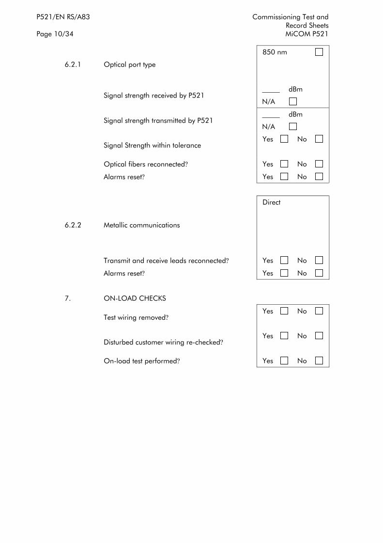
P521/EN RS/A83 Commissioning Test and Record Sheets Page 10/34 MiCOM P521
6.2.1 Optical port type
850 nm
Signal strength received by P521 dBm
N/A
Signal strength transmitted by P521 dBm
N/A
Signal Strength within tolerance Yes No
Optical fibers reconnected? Yes No
Alarms reset? Yes No
6.2.2 Metallic communications
Direct
Transmit and receive leads reconnected? Yes No
Alarms reset? Yes No
7. ON-LOAD CHECKS
Test wiring removed? Yes No
Disturbed customer wiring re-checked? Yes No
On-load test performed? Yes No

Commissioning Test and P521/EN RS/A83 Record Sheets MiCOM P521 Page 11/34
7.1 Confirm current transformer wiring
CT wiring checked? Yes No
CT polarities correct? Yes No
Phase CT ratio N/A
Earth fault CT ratio N/A
Currents: Applied value Displayed value
ΙA A A
ΙB A A
ΙC A A
ΙN A N/A A N/A
7.2 Capacitive charging current
Measured capacitive charging current
‘A’ phase A
‘B’ phase A
‘C’ phase A
Differential setting ΙS1 A
7.3 Differential current checked? Yes No
7.4 Consistency of current transformer polarity
Polarity at each end consistent?
‘A’ phase Yes No
‘B’ phase Yes No
‘C’ phase Yes No

P521/EN RS/A83 Commissioning Test and Record Sheets Page 12/34 MiCOM P521
8. FINAL CHECKS
Test wiring removed? Yes No
Disturbed customer wiring re-checked? Yes No
Commissioning test mode disabled? Yes No
Circuit breaker operations counter reset? Yes No
Current counters reset? Yes No
Event records reset? Yes No
Fault records reset? Yes No
Disturbance records reset? Yes No
Alarms reset? Yes No
LED’s reset? Yes No
Front cover replaced? Yes No
Commissioning Engineer Customer Witness
Date: Date:

Commissioning Test and P521/EN RS/A83 Record Sheets MiCOM P521 Page 13/34
2. SETTING RECORD
Date: Engineer:
Station: Circuit:
System Frequency:
Front Plate Information
Current Differential Protection Relay P521
Model Number
Serial Number
Auxiliary Voltage Vx
*Delete as appropriate
Setting Groups Used
Group 1 Yes No
Group 2 Yes No
2.1 OP Parameters
Language
Description
SERIAL NUM =
Reference
Software Version
Frequency
2.2 Configuration
2.2.1 Display
Default Display
Phase A Text
Phase B Text
Phase C Text
E/Gnd Text
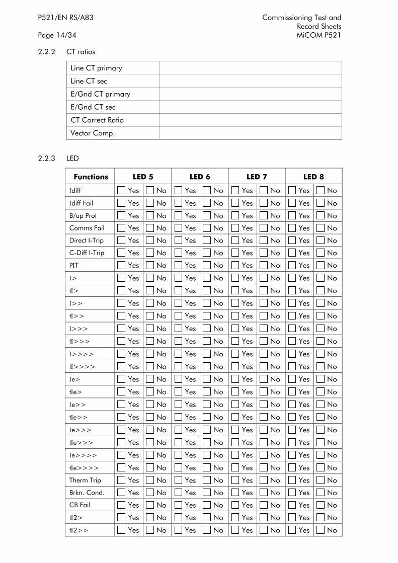
P521/EN RS/A83 Commissioning Test and Record Sheets Page 14/34 MiCOM P521
2.2.2 CT ratios
Line CT primary
Line CT sec
E/Gnd CT primary
E/Gnd CT sec
CT Correct Ratio
Vector Comp.
2.2.3 LED
Functions LED 5 LED 6 LED 7 LED 8
Ιdiff Yes No Yes No Yes No Yes No
Ιdiff Fail Yes No Yes No Yes No Yes No
B/up Prot Yes No Yes No Yes No Yes No
Comms Fail Yes No Yes No Yes No Yes No
Direct I-Trip Yes No Yes No Yes No Yes No
C-Diff I-Trip Yes No Yes No Yes No Yes No
PΙT Yes No Yes No Yes No Yes No
Ι> Yes No Yes No Yes No Yes No
tΙ> Yes No Yes No Yes No Yes No
Ι>> Yes No Yes No Yes No Yes No
tΙ>> Yes No Yes No Yes No Yes No
Ι>>> Yes No Yes No Yes No Yes No
tΙ>>> Yes No Yes No Yes No Yes No
Ι>>>> Yes No Yes No Yes No Yes No
tΙ>>>> Yes No Yes No Yes No Yes No
Ιe> Yes No Yes No Yes No Yes No
tΙe> Yes No Yes No Yes No Yes No
Ιe>> Yes No Yes No Yes No Yes No
tΙe>> Yes No Yes No Yes No Yes No
Ιe>>> Yes No Yes No Yes No Yes No
tΙe>>> Yes No Yes No Yes No Yes No
Ιe>>>> Yes No Yes No Yes No Yes No
tΙe>>>> Yes No Yes No Yes No Yes No
Therm Trip Yes No Yes No Yes No Yes No
Brkn. Cond. Yes No Yes No Yes No Yes No
CB Fail Yes No Yes No Yes No Yes No
tΙ2> Yes No Yes No Yes No Yes No
tΙ2>> Yes No Yes No Yes No Yes No

Commissioning Test and P521/EN RS/A83 Record Sheets MiCOM P521 Page 15/34
Functions LED 5 LED 6 LED 7 LED 8
Input 1 Yes No Yes No Yes No Yes No
Input 2 Yes No Yes No Yes No Yes No
Input 3 Yes No Yes No Yes No Yes No
Input 4 Yes No Yes No Yes No Yes No
Input 5 Yes No Yes No Yes No Yes No
tAux 1 Yes No Yes No Yes No Yes No
tAux 2 Yes No Yes No Yes No Yes No
CB Alarm Yes No Yes No Yes No Yes No
Equation A Yes No Yes No Yes No Yes No
Equation B Yes No Yes No Yes No Yes No
Equation C Yes No Yes No Yes No Yes No
Equation D Yes No Yes No Yes No Yes No
Equation E Yes No Yes No Yes No Yes No
Equation F Yes No Yes No Yes No Yes No
Equation G Yes No Yes No Yes No Yes No
Equation H Yes No Yes No Yes No Yes No
Prgm IT 1 Yes No Yes No Yes No Yes No
Prgm IT 2 Yes No Yes No Yes No Yes No
Prgm IT 3 Yes No Yes No Yes No Yes No
Prgm IT 4 Yes No Yes No Yes No Yes No
CTS Local Yes No Yes No Yes No Yes No
CTS Remote Yes No Yes No Yes No Yes No
CTS Block Yes No Yes No Yes No Yes No
CTS Restrain Yes No Yes No Yes No Yes No
Convention Mode Yes No Yes No Yes No Yes No
CDiff Disabled Yes No Yes No Yes No Yes No
2.2.4 Group select
Change Group Input
Setting Group
2.2.5 Alarms
Inst. Self-reset?
Comm.Fail-reset?
CDiff Disabled Alarm?
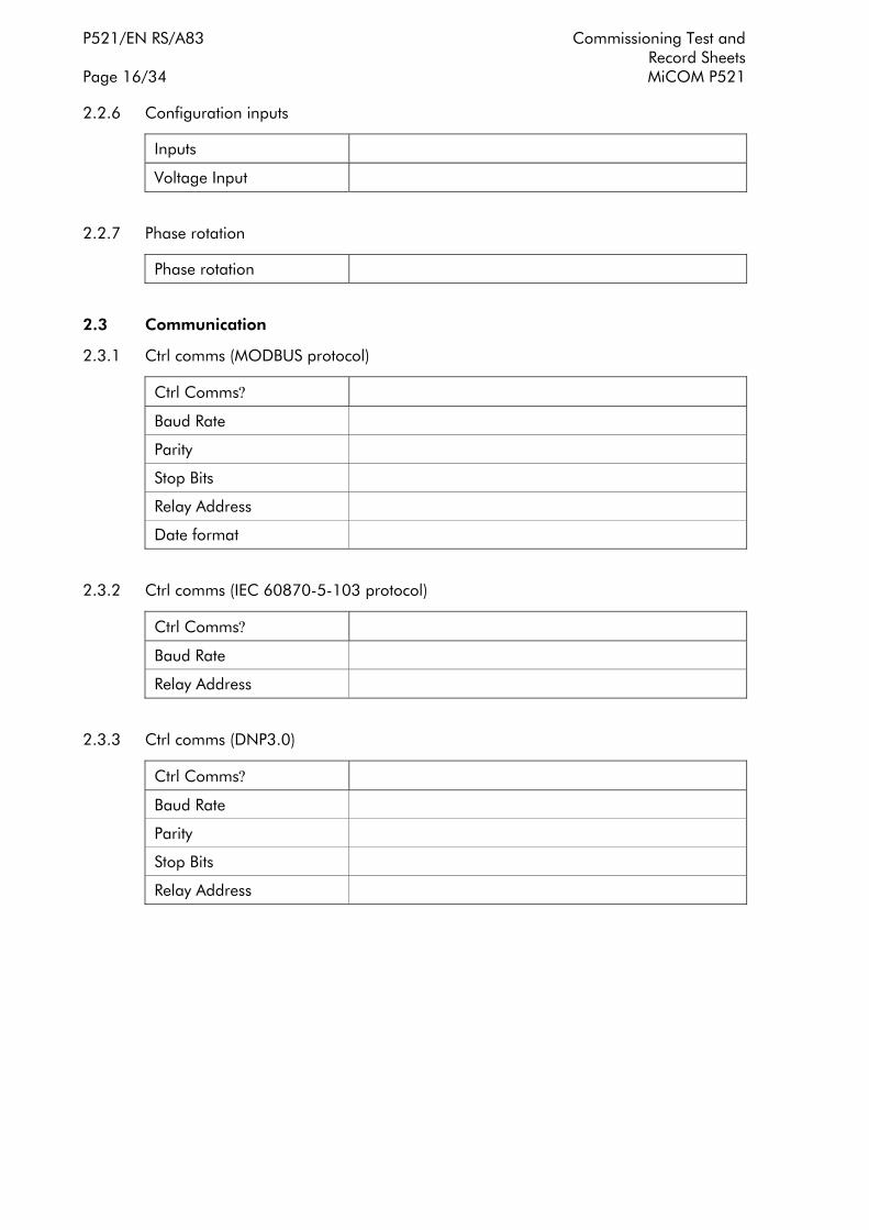
P521/EN RS/A83 Commissioning Test and Record Sheets Page 16/34 MiCOM P521
2.2.6 Configuration inputs
Inputs
Voltage Input
2.2.7 Phase rotation
Phase rotation
2.3 Communication
2.3.1 Ctrl comms (MODBUS protocol)
Ctrl Comms?
Baud Rate
Parity
Stop Bits
Relay Address
Date format
2.3.2 Ctrl comms (IEC 60870-5-103 protocol)
Ctrl Comms?
Baud Rate
Relay Address
2.3.3 Ctrl comms (DNP3.0)
Ctrl Comms?
Baud Rate
Parity
Stop Bits
Relay Address

Commissioning Test and P521/EN RS/A83 Record Sheets MiCOM P521 Page 17/34
2.3.4 Protection
Protocol
Data Rate
Relay Address
Clock Source Ch1
Comm Fail Timer
Comms Delay Tol
Char Mod Time
FRAME MODE
2.4 Protection G1/G2
2.4.1 [87] Current diff
Functions Group 1 Group 2
Current Diff?
Ιs1
Ιs2
K1
K2
Ι Diff Delay Type
tΙdiff
Ι Diff Curve
Ι Diff Tms
Ι Diff Time Dial
PΙT Time
PΙT Ι Disable
PΙT Ι Selection
PΙT Ι Threshold
DIT Rx tDwell
DIT Alarm
PIT Alarm
CTS Is1
Inrush Option
High Set
Harmonic Ratio
Kr
Transient Bias

P521/EN RS/A83 Commissioning Test and Record Sheets Page 18/34 MiCOM P521
2.4.2 [50/51] Phase O/C
Functions Group 1 Group 2
Ι>?
Ι>
Ι> Delay Type
Ι> Curve
Ι> Tms
tΙ>
Reset Type
K
tReset
Time Dial
Ι>>?
Ι>>
tΙ>> Delay Type
Ι>> Curve
Ι>> Tms
tΙ>>
Reset Type
K
tReset
Time Dial
Ι>>>?
Ι>>>
tΙ>>>
Ι>>>>?
Ι>>>>
tΙ>>>>
2.4.3 [50N/51N] E/Gnd
Functions Group 1 Group 2
Ιe>?
Ιe>
Ιe> Delay Type
Ιe> Curve
Ιe> Tms

Commissioning Test and P521/EN RS/A83 Record Sheets MiCOM P521 Page 19/34
tΙe>
Reset Type
K
tReset
Time Dial
Ιe>>?
Ιe>>
tΙe>> Delay Type
Ιe> Curve
Ιe>> Tms
tΙe>>
Reset Type
K
tReset
Time Dial
Ιe>>>?
Ιe>>>
tΙe>>>
Ιe>>>>?
Ιe>>>>
tΙe>>>>
2.4.4 [46] Neg seq OC
Functions Group 1 Group 2
Ι2>?
Ι2>
Ι2> Delay Type
Ι2> Curve
Ι2> Tms
tΙ2>
Reset Type
K
tReset
Time Dial
t Reset
Ι2>>?
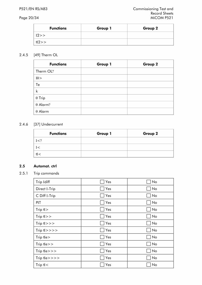
P521/EN RS/A83 Commissioning Test and Record Sheets Page 20/34 MiCOM P521
Functions Group 1 Group 2
Ι2>>
tΙ2>>
2.4.5 [49] Therm OL
Functions Group 1 Group 2
Therm OL?
Ιθ>
Te
k
θ Trip
θ Alarm?
θ Alarm
2.4.6 [37] Undercurrent
Functions Group 1 Group 2
Ι<?
Ι<
tΙ<
2.5 Automat. ctrl
2.5.1 Trip commands
Trip Ιdiff Yes No
Direct Ι-Trip Yes No
C Diff Ι-Trip Yes No
PΙT Yes No
Trip tΙ> Yes No
Trip tΙ>> Yes No
Trip tΙ>>> Yes No
Trip tΙ>>>> Yes No
Trip tΙe> Yes No
Trip tΙe>> Yes No
Trip tΙe>>> Yes No
Trip tΙe>>>> Yes No
Trip tΙ< Yes No
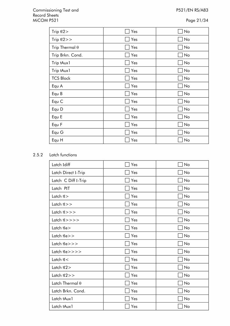
Commissioning Test and P521/EN RS/A83 Record Sheets MiCOM P521 Page 21/34
Trip tΙ2> Yes No
Trip tΙ2>> Yes No
Trip Thermal θ Yes No
Trip Brkn. Cond. Yes No
Trip tAux1 Yes No
Trip tAux1 Yes No
TCS Block Yes No
Equ A Yes No
Equ B Yes No
Equ C Yes No
Equ D Yes No
Equ E Yes No
Equ F Yes No
Equ G Yes No
Equ H Yes No
2.5.2 Latch functions
Latch Ιdiff Yes No
Latch Direct Ι-Trip Yes No
Latch C Diff Ι-Trip Yes No
Latch PΙT Yes No
Latch tΙ> Yes No
Latch tΙ>> Yes No
Latch tΙ>>> Yes No
Latch tΙ>>>> Yes No
Latch tΙe> Yes No
Latch tΙe>> Yes No
Latch tΙe>>> Yes No
Latch tΙe>>>> Yes No
Latch tΙ< Yes No
Latch tΙ2> Yes No
Latch tΙ2>> Yes No
Latch Thermal θ Yes No
Latch Brkn. Cond. Yes No
Latch tAux1 Yes No
Latch tAux1 Yes No

P521/EN RS/A83 Commissioning Test and Record Sheets Page 22/34 MiCOM P521
TCS Block Yes No
Equ A Yes No
Equ B Yes No
Equ C Yes No
Equ D Yes No
Equ E Yes No
Equ F Yes No
Equ G Yes No
Equ H Yes No
2.5.3 Blocking logic 1/2
Functions Blocking Logic 1 Blocking Logic 2
Block Ιdiff Yes No Yes No
Block tΙ> Yes No Yes No
Block tΙ>> Yes No Yes No
Block tΙ>>> Yes No Yes No
Block tΙ>>>> Yes No Yes No
Block tΙe> Yes No Yes No
Block tΙe>> Yes No Yes No
Block tΙe>>> Yes No Yes No
Block tΙe>>>> Yes No Yes No
Block tΙ2> Yes No Yes No
Block tΙ2>> Yes No Yes No
Block Thermal θ Yes No Yes No
Block Brkn. Cond. Yes No Yes No
Block tAux 1 Yes No Yes No
Block tAux 2 Yes No Yes No
Equ A Yes No Yes No
Equ B Yes No Yes No
Equ C Yes No Yes No
Equ D Yes No Yes No
Equ E Yes No Yes No
Equ F Yes No Yes No
Equ G Yes No Yes No
Equ H Yes No Yes No

Commissioning Test and P521/EN RS/A83 Record Sheets MiCOM P521 Page 23/34
2.5.4 Logic select 1/2
Functions Logic Select 1 Logic Select 2
Sel tΙ>> Yes No Yes No
Sel tΙ>>> Yes No Yes No
Sel tΙ>>>> Yes No Yes No
Sel tΙe>> Yes No Yes No
Sel tΙe>>> Yes No Yes No
Sel tΙe>>>> Yes No Yes No
tSel 1
2.5.5 Output relays
Functions Setting Functions Setting
Trip Brkn. Cond.
ΙDiff CB fail
Back-up Prot. CB Close
Comms Fail tAux1
Direct Ι-Trip tAux2
C-Diff Ι-Trip Active Group
PΙT TCS Block
Ι> Input1
tΙ> Input2
Ι>> Input3
tΙ>> Input4
Ι>>> Input5
tΙ>>> Equ A
Ι>>>> Equ B
tΙ>>>> Equ C
Ιe> Equ D
tΙe> Equ E
Ιe>> Equ F
tΙe>> Equ G
Ιe>>> Equ H
tΙe>>> Prgm I-Trip1
Ιe>>>> Prgm I-Trip2
tΙe>>>> Prgm I-Trip3
tΙ< Prgm I-Trip4

P521/EN RS/A83 Commissioning Test and Record Sheets Page 24/34 MiCOM P521
Functions Setting Functions Setting
tΙ2> CTS Local
tΙ2>> CTS Remote
Therm Alarm CTS Block
Therm Trip CTS Res.
CB Alarm Mode Convent
52 Fail CDiff Disable
2.5.6 Latch output relays
Output 2 Yes No
Output 3 Yes No
Output 4 Yes No
Output 5 Yes No
Output 6 Yes No
Output 7 Yes No
Output 8 Yes No
2.5.7 Invert output relays
Output 2 Yes No
Output 3 Yes No
Output 4 Yes No
Output 5 Yes No
Output 6 Yes No
Output 7 Yes No
Output 8 Yes No
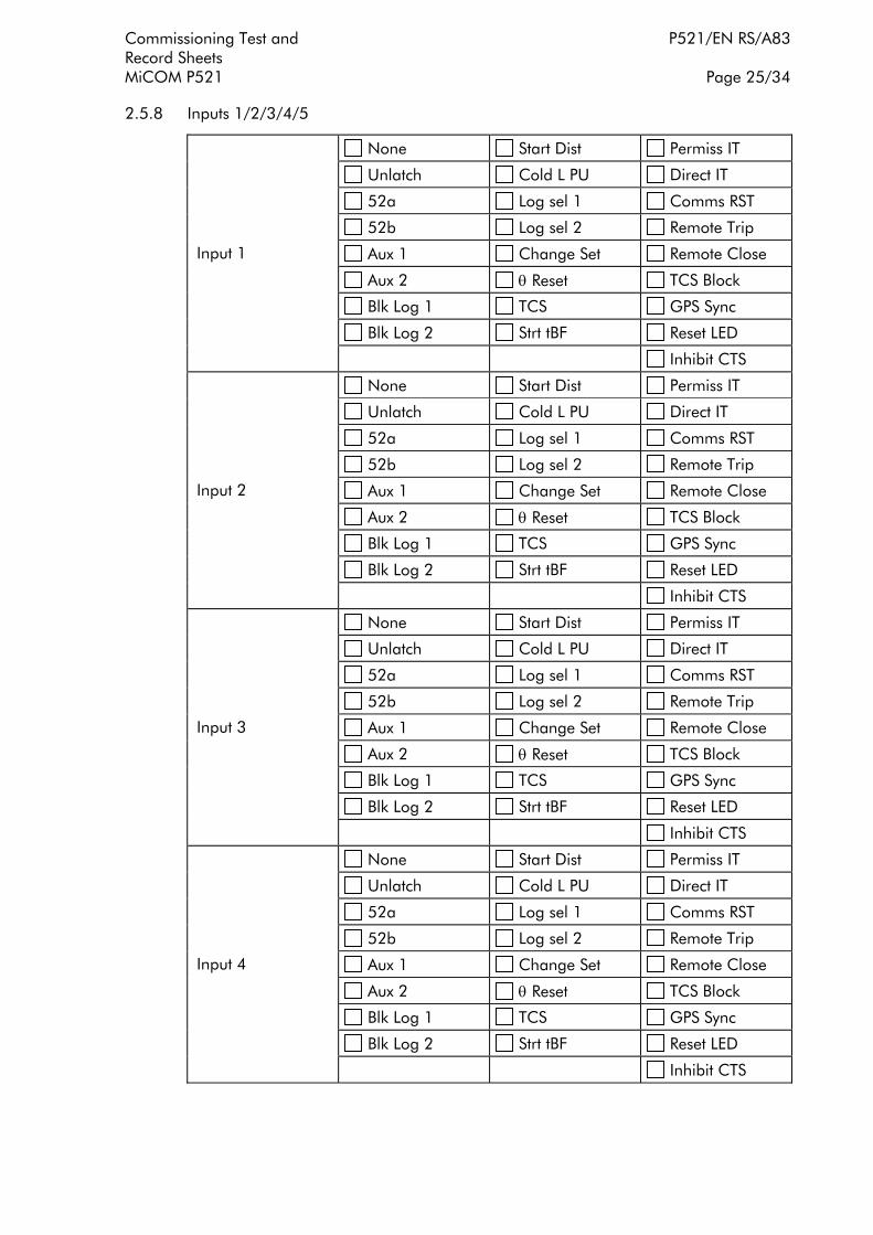
Commissioning Test and P521/EN RS/A83 Record Sheets MiCOM P521 Page 25/34
2.5.8 Inputs 1/2/3/4/5
None Start Dist Permiss IT
Unlatch Cold L PU Direct IT
52a Log sel 1 Comms RST
52b Log sel 2 Remote Trip
Aux 1 Change Set Remote Close
Aux 2 θ Reset TCS Block
Blk Log 1 TCS GPS Sync
Blk Log 2 Strt tBF Reset LED
Input 1
Inhibit CTS
None Start Dist Permiss IT
Unlatch Cold L PU Direct IT
52a Log sel 1 Comms RST
52b Log sel 2 Remote Trip
Aux 1 Change Set Remote Close
Aux 2 θ Reset TCS Block
Blk Log 1 TCS GPS Sync
Blk Log 2 Strt tBF Reset LED
Input 2
Inhibit CTS
None Start Dist Permiss IT
Unlatch Cold L PU Direct IT
52a Log sel 1 Comms RST
52b Log sel 2 Remote Trip
Aux 1 Change Set Remote Close
Aux 2 θ Reset TCS Block
Blk Log 1 TCS GPS Sync
Blk Log 2 Strt tBF Reset LED
Input 3
Inhibit CTS
None Start Dist Permiss IT
Unlatch Cold L PU Direct IT
52a Log sel 1 Comms RST
52b Log sel 2 Remote Trip
Aux 1 Change Set Remote Close
Aux 2 θ Reset TCS Block
Blk Log 1 TCS GPS Sync
Blk Log 2 Strt tBF Reset LED
Input 4
Inhibit CTS

P521/EN RS/A83 Commissioning Test and Record Sheets Page 26/34 MiCOM P521
None Start Dist Permiss IT
Unlatch Cold L PU Direct IT
52a Log sel 1 Comms RST
52b Log sel 2 Remote Trip
Aux 1 Change Set Remote Close
Aux 2 θ Reset TCS Block
Blk Log 1 TCS GPS Sync
Blk Log 2 Strt tBF Reset LED
Input 5
Inhibit CTS
Aux 1 Time tAux1
Aux 2 Time tAux2
2.5.9 Brkn. cond
Brkn. Cond?
Brkn. Cond. Time tBC
Ratio Ι2/Ι1
2.5.10 Cold load pu
Cold Load PU? Yes No
tΙ>? Yes No
tΙ>>? Yes No
tΙ>>>? Yes No
tΙ>>>>? Yes No
tΙe>? Yes No
tΙe>>? Yes No
tΙe>>>? Yes No
tΙe>>>>? Yes No
tΙ2>? Yes No
tΙ2>>? Yes No
t Therm? Yes No
Cold Load PU Level
Cold Load tCL

Commissioning Test and P521/EN RS/A83 Record Sheets MiCOM P521 Page 27/34
2.5.11 CB fail
CB Fail?
Ι< =
CB Fail Time tBF
Block Ι>
Block Ιe>
2.5.12 CB supervision
TC Supervision?
t tripcircuit tSUP
CB Open S’vision
CB Open Time
CB Close S’vision
CB Close Time
CB Close Alarm?
CB Open NB
Σ Amps(n)?
Σ Amps(n)
n
t Open Pulse
t Close Pulse
CB Man Trip Dly
CB Man Close Dly
2.5.13 Logic Equations
Equ. A Boolean Logic operand
A.00 =/ = NOT
A.01 OR / OR NOT / AND / AND NOT
A.02 OR / OR NOT / AND / AND NOT
A.03 OR / OR NOT / AND / AND NOT
A.04 OR / OR NOT / AND / AND NOT
A.05 OR / OR NOT / AND / AND NOT
A.06 OR / OR NOT / AND / AND NOT
A.07 OR / OR NOT / AND / AND NOT
A.08 OR / OR NOT / AND / AND NOT
A.09 OR / OR NOT / AND / AND NOT

P521/EN RS/A83 Commissioning Test and Record Sheets Page 28/34 MiCOM P521
Equ. A Boolean Logic operand
A.10 OR / OR NOT / AND / AND NOT
A.11 OR / OR NOT / AND / AND NOT
A.12 OR / OR NOT / AND / AND NOT
A.13 OR / OR NOT / AND / AND NOT
A.14 OR / OR NOT / AND / AND NOT
A.15 OR / OR NOT / AND / AND NOT
T Operate ms
T Reset ms
Equ. B Boolean Logic operand
B.00 =/ = NOT
B.01 OR / OR NOT / AND / AND NOT
B.02 OR / OR NOT / AND / AND NOT
B.03 OR / OR NOT / AND / AND NOT
B.04 OR / OR NOT / AND / AND NOT
B.05 OR / OR NOT / AND / AND NOT
B.06 OR / OR NOT / AND / AND NOT
B.07 OR / OR NOT / AND / AND NOT
B.08 OR / OR NOT / AND / AND NOT
B.09 OR / OR NOT / AND / AND NOT
B.10 OR / OR NOT / AND / AND NOT
B.11 OR / OR NOT / AND / AND NOT
B.12 OR / OR NOT / AND / AND NOT
B.13 OR / OR NOT / AND / AND NOT
B.14 OR / OR NOT / AND / AND NOT
B.15 OR / OR NOT / AND / AND NOT
T Operate ms
T Reset ms
Equ. C Boolean Logic operand
C.00 =/ = NOT
C.01 OR / OR NOT / AND / AND NOT
C.02 OR / OR NOT / AND / AND NOT
C.03 OR / OR NOT / AND / AND NOT
C.04 OR / OR NOT / AND / AND NOT
C.05 OR / OR NOT / AND / AND NOT
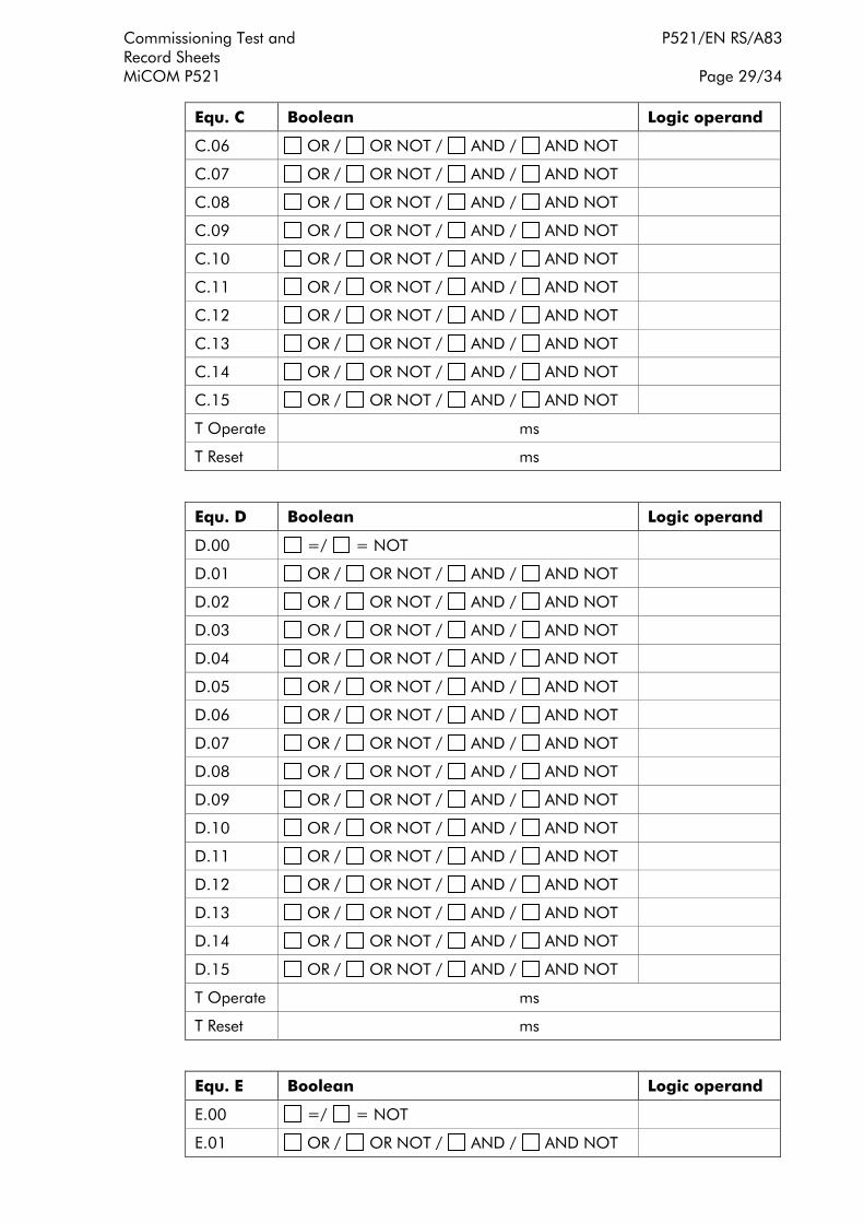
Commissioning Test and P521/EN RS/A83 Record Sheets MiCOM P521 Page 29/34
Equ. C Boolean Logic operand
C.06 OR / OR NOT / AND / AND NOT
C.07 OR / OR NOT / AND / AND NOT
C.08 OR / OR NOT / AND / AND NOT
C.09 OR / OR NOT / AND / AND NOT
C.10 OR / OR NOT / AND / AND NOT
C.11 OR / OR NOT / AND / AND NOT
C.12 OR / OR NOT / AND / AND NOT
C.13 OR / OR NOT / AND / AND NOT
C.14 OR / OR NOT / AND / AND NOT
C.15 OR / OR NOT / AND / AND NOT
T Operate ms
T Reset ms
Equ. D Boolean Logic operand
D.00 =/ = NOT
D.01 OR / OR NOT / AND / AND NOT
D.02 OR / OR NOT / AND / AND NOT
D.03 OR / OR NOT / AND / AND NOT
D.04 OR / OR NOT / AND / AND NOT
D.05 OR / OR NOT / AND / AND NOT
D.06 OR / OR NOT / AND / AND NOT
D.07 OR / OR NOT / AND / AND NOT
D.08 OR / OR NOT / AND / AND NOT
D.09 OR / OR NOT / AND / AND NOT
D.10 OR / OR NOT / AND / AND NOT
D.11 OR / OR NOT / AND / AND NOT
D.12 OR / OR NOT / AND / AND NOT
D.13 OR / OR NOT / AND / AND NOT
D.14 OR / OR NOT / AND / AND NOT
D.15 OR / OR NOT / AND / AND NOT
T Operate ms
T Reset ms
Equ. E Boolean Logic operand
E.00 =/ = NOT
E.01 OR / OR NOT / AND / AND NOT

P521/EN RS/A83 Commissioning Test and Record Sheets Page 30/34 MiCOM P521
Equ. E Boolean Logic operand
E.02 OR / OR NOT / AND / AND NOT
E.03 OR / OR NOT / AND / AND NOT
E.04 OR / OR NOT / AND / AND NOT
E.05 OR / OR NOT / AND / AND NOT
E.06 OR / OR NOT / AND / AND NOT
E.07 OR / OR NOT / AND / AND NOT
E.08 OR / OR NOT / AND / AND NOT
E.09 OR / OR NOT / AND / AND NOT
E.10 OR / OR NOT / AND / AND NOT
E.11 OR / OR NOT / AND / AND NOT
E.12 OR / OR NOT / AND / AND NOT
E.13 OR / OR NOT / AND / AND NOT
E.14 OR / OR NOT / AND / AND NOT
E.15 OR / OR NOT / AND / AND NOT
T Operate ms
T Reset ms
Equ. F Boolean Logic operand
F.00 =/ = NOT
F.01 OR / OR NOT / AND / AND NOT
F.02 OR / OR NOT / AND / AND NOT
F.03 OR / OR NOT / AND / AND NOT
F.04 OR / OR NOT / AND / AND NOT
F.05 OR / OR NOT / AND / AND NOT
F.06 OR / OR NOT / AND / AND NOT
F.07 OR / OR NOT / AND / AND NOT
F.08 OR / OR NOT / AND / AND NOT
F.09 OR / OR NOT / AND / AND NOT
F.10 OR / OR NOT / AND / AND NOT
F.11 OR / OR NOT / AND / AND NOT
F.12 OR / OR NOT / AND / AND NOT
F.13 OR / OR NOT / AND / AND NOT
F.14 OR / OR NOT / AND / AND NOT
F.15 OR / OR NOT / AND / AND NOT
T Operate ms
T Reset ms
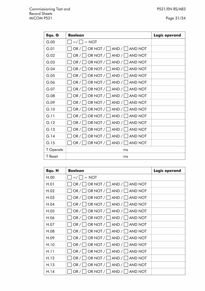
Commissioning Test and P521/EN RS/A83 Record Sheets MiCOM P521 Page 31/34
Equ. G Boolean Logic operand
G.00 =/ = NOT
G.01 OR / OR NOT / AND / AND NOT
G.02 OR / OR NOT / AND / AND NOT
G.03 OR / OR NOT / AND / AND NOT
G.04 OR / OR NOT / AND / AND NOT
G.05 OR / OR NOT / AND / AND NOT
G.06 OR / OR NOT / AND / AND NOT
G.07 OR / OR NOT / AND / AND NOT
G.08 OR / OR NOT / AND / AND NOT
G.09 OR / OR NOT / AND / AND NOT
G.10 OR / OR NOT / AND / AND NOT
G.11 OR / OR NOT / AND / AND NOT
G.12 OR / OR NOT / AND / AND NOT
G.13 OR / OR NOT / AND / AND NOT
G.14 OR / OR NOT / AND / AND NOT
G.15 OR / OR NOT / AND / AND NOT
T Operate ms
T Reset ms
Equ. H Boolean Logic operand
H.00 =/ = NOT
H.01 OR / OR NOT / AND / AND NOT
H.02 OR / OR NOT / AND / AND NOT
H.03 OR / OR NOT / AND / AND NOT
H.04 OR / OR NOT / AND / AND NOT
H.05 OR / OR NOT / AND / AND NOT
H.06 OR / OR NOT / AND / AND NOT
H.07 OR / OR NOT / AND / AND NOT
H.08 OR / OR NOT / AND / AND NOT
H.09 OR / OR NOT / AND / AND NOT
H.10 OR / OR NOT / AND / AND NOT
H.11 OR / OR NOT / AND / AND NOT
H.12 OR / OR NOT / AND / AND NOT
H.13 OR / OR NOT / AND / AND NOT
H.14 OR / OR NOT / AND / AND NOT

P521/EN RS/A83 Commissioning Test and Record Sheets Page 32/34 MiCOM P521
Equ. H Boolean Logic operand
H.15 OR / OR NOT / AND / AND NOT
T Operate ms
T Reset ms
2.5.14 Program. I-Trip
tI> tI2> Input 5
tI>> tI2>> Equ A
tI>>> CB Fail Equ B
tI>>>> Broken Cond. Equ C
tIe> tAux1 Equ D
tIe>> tAux2 Equ E
tIe>>> Input 1 Equ F
tIe>>>> Input 2 Equ G
Therm Trip Input 3 Equ H
Program. I-Trip1
tI< Input 4
tI> tI2> Input 5
tI>> tI2>> Equ A
tI>>> CB Fail Equ B
tI>>>> Broken Cond. Equ C
tIe> tAux1 Equ D
tIe>> tAux2 Equ E
tIe>>> Input 1 Equ F
tIe>>>> Input 2 Equ G
Therm Trip Input 3 Equ H
Program. I-Trip2
tI< Input 4
tI> tI2> Input 5
tI>> tI2>> Equ A
tI>>> CB Fail Equ B
tI>>>> Broken Cond. Equ C
tIe> tAux1 Equ D
tIe>> tAux2 Equ E
tIe>>> Input 1 Equ F
tIe>>>> Input 2 Equ G
Therm Trip Input 3 Equ H
Program. I-Trip3
tI< Input 4
tI> tI2> Input 5
tI>> tI2>> Equ A
tI>>> CB Fail Equ B
Program. I-Trip4
tI>>>> Broken Cond. Equ C

Commissioning Test and P521/EN RS/A83 Record Sheets MiCOM P521 Page 33/34
tIe> tAux1 Equ D
tIe>> tAux2 Equ E
tIe>>> Input 1 Equ F
tIe>>>> Input 2 Equ G
Therm Trip Input 3 Equ H
tI< Input 4
tI> tI2> Input 5
tI>> tI2>> Equ A
tI>>> CB Fail Equ B
tI>>>> Broken Cond. Equ C
tIe> tAux1 Equ D
tIe>> tAux2 Equ E
tIe>>> Input 1 Equ F
tIe>>>> Input 2 Equ G
Therm Trip Input 3 Equ H
Program. I-Trip5
tI< Input 4
Dwell Timer
2.5.15 CT supervision
CTS?
CTS Reset mode
CTS I1>
CTS I2/I1>
CTS I2/I1>>
CTS TIME DLY
CTS Restrain?
2.6 Records
2.6.1 Disturb record
Record Number
Pre-time
Disturb Rec Trig
2.6.2 Time peak value
Time Window

P521/EN RS/A83 Commissioning Test and Record Sheets Page 34/34 MiCOM P521
2.6.3 Rolling demand
Sub Period
Num of Sub Per
Commissioning Engineer Customer Witness
Date: Date:

Hardware/Software Version P521/EN VC/A83 History and Compatibility MiCOM P521
HARDWARE/SOFTWARE VERSION HISTORY AND COMPATIBILITY
Date: 1st October 2010
Software version: 12
Connection diagram: 10P52101


Hardw
are/Software Version
P521/EN
VC/A
83 H
istory and Com
patibility
M
iCO
M P521
Page 1/6
Relay type: P521 …
Software Version
Major Minor
Hardware Suffix
Original Date of Issue
Description of Changes S1
Compatibility Technical
Documentation
A A Jul 2003 Original Issue V2.09 or Later P521/EN M/B11
B A Oct 2003
Current differential blocking logic functionality changed to inhibit protection timer when blocking enabled. This fix prevents the current differential from mal-tripping upon removal of the blocking input
V2.09 or Later P521/EN M/B11
C A Apr 2004
Modification to ensure that the loopback alarm is re-instated following an interruption to the auxiliary supply
Enhancement to prevent both manual trip and close commands from operating simultaneously
Modification to summation amps function in order to improve measurement accuracy
Correction to fault records to include the magnitude of negative sequence current when the Ι2>> element operates
Modification to allow fault records to be acknowledged via remote communications
Improvements made to setting group 2 dependencies to ensure all menu cells are displayed correctly
Enhancement to allow the contact test, in the commissioning menu, to be operated via remote communications
V2.09 or Later P521/EN M/B11
1
D A Jun 2004 Correction to ensure erroneous ΙDIFF FAIL alarms not
generated V2.09 or Later P521/EN AD/B21

P521/EN VC
/A83
H
ardware/Softw
are Version
H
istory and Com
patibility Page 2/6
M
iCO
M P521
Relay type: P521 …
Software Version
Major Minor
Hardware Suffix
Original Date of Issue
Description of Changes S1
Compatibility Technical
Documentation
F A Nov 2005 Improved compatibility with P59x units V2.09 or Later P521/EN AD/B21 1
cont. G A Jun 2006 Correction to ensure correct CB fail operation when
tBFtimer < 180 ms V2.09 or Later P521/EN AD/B21
A A Jun 2005
k1 setting minimum value changed to 0 %
Vector compensation added for transformer applications
High Set added for inrush restraint
Selective intertripping added
Output contact inversion settings added
Extended protection communication addresses (increased to 20)
Correction to ensure new alarms do cause front panel LCD to jump to alarms display, unless on default display
IEC 60870-5-103 GI expanded and sequence corrected
V2.11 or Later P521/EN M/C31
B A Nov 2005 Improved compatibility with P59x units V2.11 or Later P521/EN M/C31
C A Mar 2006
IEC 60870-5-103 GI sequence number in end of GI message corrected
IEC 60870-5-103 Blocking of P922 relays after time synchronization corrected
V2.11 or Later P521/EN M/C31
2
D A Jun 2006 Correction to ensure correct CB fail operation when
tBFtimer < 180 ms V2.11 or Later P521/EN M/C31
3 A A Mar 2007
DNP3.0 protocol option added
Phase angle measurements added
PIT current check functionality modified, including addition of local current check option
External TCS Block function added for H7 compliance
V2.13 or Later P521/EN AD/C41
Hardw
are/Software Version
P521/EN
VC/A
83 H
istory and Com
patibility
M
iCO
M P521
Page 3/6
Relay type: P521 …
Software Version
Major Minor
Hardware Suffix
Original Date of Issue
Description of Changes S1
Compatibility Technical
Documentation
Additional Phase label settings added
Password reset via front panel added
Comms Alarm self reset setting added
Transient Bias functionality added to mitigate CT saturation
Modified Reference to ‘MiCO’ (front panel and Modbus) and identification to ‘MiCOM P521’ (IEC60870-5-103)
Russian language option for front panel added
Correction of Vector Compensation groups Yy2 and Yy10
4 A A July 2007 PIT & DIT Alarm Enabled/Disabled added V2.13 or later P521/EN AD/C51
5 A A February 2010 New version enabling the setting of 2nd harmonic
restraint factor. Studio 3.1
5 B A June 2010 New version resolving the incompatibility problem
between phase 1 and phase 2. Studio 3.1
10 A B August 2009 Upgraded into Phase 2 Studio 3.1 P521/EN M/C63
11 A B February 2010 New version enabling the setting of 2nd harmonic
restraint factor. Studio 3.1
12 B B October
New version with software enhancements:
CTS
Programmable inter-trip
Boolean logic equations
Studio 3.1

P521/EN VC
/A83
H
ardware/Softw
are Version
H
istory and Com
patibility Page 4/6
M
iCO
M P521
Relay Communication Compatibility Table
Relay software version
1.A 1.B 1.C 1.D 1.F 1.G 2.A 2.B 2.C 2.D 3.A 4.A 5.A 5.B 10.A 11.A 12.B
1.A
1.B
1.C
1.D
1.F
2.A
2.B
2.C
2.D
3.A
4.A
5.A
5.B
10.A
11.A
Rela
y so
ftwar
e ve
rsio
n
12.B
Hardware/Software Version P521/EN VC/A83 History and Compatibility MiCOM P521 Page 5/6
Information Required with Order
P 5 2 1 A 0 A A 1 0 1 1 0
MiCOM Range Protection and control
P
Device Type Current Differential Protection
5
Platform x20 Platform
2
Model Standard (2 ended)
1
E/F CT Rating 0.1 - 40 Ιon A 0.01 - 8 Ιon B 0.002 - 1 Ιon C
Not used
Default 0
Protection Communication
EIA (RS) 232 single channel A
EIA (RS) 485 single channel B
850 nm single channel C
1300 nm multi-mode/single channel (27 dB) Obsolete from July 2009
D
1300 nm single-mode/single channel (27 dB) Obsolete from July 2009
E
1300 nm multi-mode/single channel (43 dB) F
1300 nm single-mode/single channel (43 dB) G
Auxiliary Power Supply
Digital Input Voltage
24 - 60 Vdc 24 - 250 Vdc/24 - 240 Vac
A
48 – 250 Vdc/48- 240 Vac
24 - 250 Vdc/24 - 240 Vac
F
48 – 250 Vdc/48- 240 Vac Special EA
24 - 250 Vdc/24 - 240 Vac
T
48 – 250 Vdc/48- 240 Vac
129 Vdc H
48 – 250 Vdc/48- 240 Vac 110 Vdc V
48 – 250 Vdc/48- 240 Vac
220 Vdc W
Communication Protocol
MODBUS 1
IEC 60870-5-103 3
DNP3 4

P521/EN VC/A83 Hardware/Software Version History and Compatibility Page 6 of 6 MiCOM P521
P 5 2 1 A 0 A A 1 0 1 1 0
Language
French
English/American
Spanish
German
Italian
Russian
Polish
Portuguese – Not yet available
Dutch – Not yet available
Czech – Not yet available
Hungarian – Not yet available
Greek – Not yet available
Chinese
Turkish – Not yet available
0
1
2
3
4
5
6
7
8
A
B
C
D
E
Platform
Phase 1
Phase 2
Phase 2 with large graph
1
2
3
Software Version 12


Schneider Electric 35 rue Joseph Monier 92506 Rueil-Malmaison FRANCE
Phone: +33 (0) 1 41 29 70 00 Fax: +33 (0) 1 41 29 71 00 www.schneider-electric.com Publishing: Schneider Electric
Publication: P521/EN M/A83 SV.12 HS.B 11/2010
© 2
010
Sch
neid
er E
lect
ric. A
ll rig
hts
rese
rved
.