MIC2044/2045 Micrel MIC2044/2045
15
January 2005 1 MIC2044/2045 MIC2044/2045 Single Channel, High Current, Low Voltage, Protected Power Distribution Switch General Description The MIC2044 and MIC2045 are high-side MOSFET switches optimized for general purpose power distribution applications that require circuit protection. These devices switch up to 5.5V and as low as 0.8V while offering both programmable current limiting and thermal shutdown to protect the device and the load. A fault status output is provided to indicate overcurrent and thermal shutdown fault conditions. Both devices employ soft-start circuitry to minimize the inrush current in applications that employ highly capacitive loads. Additionally, for tighter control over inrush current during start up, the output slew-rate may be adjusted by an external capacitor. The MIC2045 features a auto-reset circuit breaker that latches the output OFF upon detecting an overcurrent condition lasting more than 32ms. The output is reset by removing or reducing the load. Data sheets and support documentation can be found on Micrel’s web site at www.micrel.com. Typical Application "Applications Information." Features • 30mΩ maximum on-resistance • 0.8V to 5.5V operating range • Adjustable current limit • Up to 6A continuous output current • Short circuit protection • Very fast reaction to short circuits • Thermal shutdown • Adjustable slew-rate control • Circuit breaker mode (MIC2045) • Fault status flag • Power-Good detection • Undervoltage lockout • No reverse current flow through the switching MOSFET when OFF or disabled • Low quiescent current Applications • Docking stations • LAN servers • WAN switches • Hot swap board insertions • Notebook PCs • PDAs • Base stations • RAID controllers • USB hosts Micrel, Inc. • 1849 Fortune Drive • San Jose, CA 95131 • USA • tel + 1 (408) 944-0800 • fax + 1 (408) 944-0970 • http://www.micrel.com
Transcript of MIC2044/2045 Micrel MIC2044/2045

January 2005 1 MIC2044/2045
MIC2044/2045 Micrel
MIC2044/2045Single Channel, High Current, Low Voltage,
Protected Power Distribution Switch
General DescriptionThe MIC2044 and MIC2045 are high-side MOSFET switchesoptimized for general purpose power distribution applicationsthat require circuit protection. These devices switch up to5.5V and as low as 0.8V while offering both programmablecurrent limiting and thermal shutdown to protect the deviceand the load. A fault status output is provided to indicateovercurrent and thermal shutdown fault conditions. Bothdevices employ soft-start circuitry to minimize the inrushcurrent in applications that employ highly capacitive loads.Additionally, for tighter control over inrush current during startup, the output slew-rate may be adjusted by an externalcapacitor.
The MIC2045 features a auto-reset circuit breaker that latchesthe output OFF upon detecting an overcurrent conditionlasting more than 32ms. The output is reset by removing orreducing the load.
Data sheets and support documentation can be found onMicrel’s web site at www.micrel.com.
Typical Application
! " #$%& ' ()$*
+, ! " #$%& ' ()$*
-. / *
+!! 01$23' / **
45 %* "Applications Information."
54*6
5*6
-(75$$
+8+66
+5,
9
86,-
-.
-:*
+,
036
0:3;
,-+
3;
<
<=
*<=
3;
+,
5-+;6
+,*> *
<
+0
?*01$ !&
+, +,
5*6
5*6
Features• 30mΩ maximum on-resistance• 0.8V to 5.5V operating range• Adjustable current limit• Up to 6A continuous output current• Short circuit protection• Very fast reaction to short circuits• Thermal shutdown• Adjustable slew-rate control• Circuit breaker mode (MIC2045)• Fault status flag• Power-Good detection• Undervoltage lockout• No reverse current flow through the switching MOSFET
when OFF or disabled• Low quiescent current
Applications• Docking stations• LAN servers• WAN switches• Hot swap board insertions• Notebook PCs• PDAs• Base stations• RAID controllers• USB hosts
Micrel, Inc. • 1849 Fortune Drive • San Jose, CA 95131 • USA • tel + 1 (408) 944-0800 • fax + 1 (408) 944-0970 • http://www.micrel.com
MIC2044/2045 Micrel
MIC2044/2045 2 January 2005
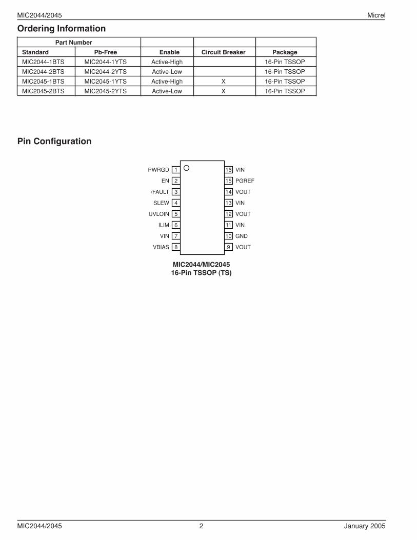
Pin Configuration
1PWRGD
EN
/FAULT
SLEW
UVLOIN
ILIM
VIN
VBIAS
16 VIN
PGREF
VOUT
VIN
VOUT
VIN
GND
VOUT
15
14
13
12
11
10
9
2
3
4
5
6
7
8
MIC2044/MIC204516-Pin TSSOP (TS)
Ordering InformationPart Number
Standard Pb-Free Enable Circuit Breaker Package
MIC2044-1BTS MIC2044-1YTS Active-High 16-Pin TSSOP
MIC2044-2BTS MIC2044-2YTS Active-Low 16-Pin TSSOP
MIC2045-1BTS MIC2045-1YTS Active-High X 16-Pin TSSOP
MIC2045-2BTS MIC2045-2YTS Active-Low X 16-Pin TSSOP
January 2005 3 MIC2044/2045
MIC2044/2045 Micrel
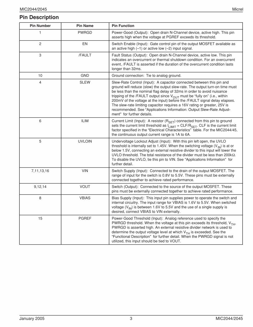
Pin DescriptionPin Number Pin Name Pin Function
1 PWRGD Power-Good (Output): Open drain N-Channel device, active high. This pinasserts high when the voltage at PGREF exceeds its threshold.
2 EN Switch Enable (Input): Gate control pin of the output MOSFET available asan active high (–1) or active low (–2) input signal.
3 /FAULT Fault Status (Output): Open drain N-Channel device, active low. This pinindicates an overcurrent or thermal shutdown condition. For an overcurrentevent, /FAULT is asserted if the duration of the overcurrent condition lastslonger than 32ms.
10 GND Ground connection: Tie to analog ground.
4 SLEW Slew-Rate Control (Input): A capacitor connected between this pin andground will reduce (slow) the output slew-rate. The output turn-on time mustbe less than the nominal flag delay of 32ms in order to avoid nuisancetripping of the /FAULT output since VOUT must be “fully on” (i.e., within200mV of the voltage at the input) before the /FAULT signal delay elapses.The slew-rate limiting capacitor requires a 16V rating or greater, 25V isrecommended. See “Applications Information: Output Slew-Rate Adjust-ment” for further details.
6 ILIM Current Limit (Input): A resistor (RSET) connected from this pin to groundsets the current limit threshold as ILIMIT = CLF/RSET. CLF is the current limitfactor specified in the “Electrical Characteristics” table. For the MIC2044/45,the continuous output current range is 1A to 6A.
5 UVLOIN Undervoltage Lockout Adjust (Input): With this pin left open, the UVLOthreshold is internally set to 1.45V. When the switching voltage (VIN) is at orbelow 1.5V, connecting an external resistive divider to this input will lower theUVLO threshold. The total resistance of the divider must be less than 200kΩ.To disable the UVLO, tie this pin to VIN. See “Applications Information” forfurther detail.
7,11,13,16 VIN Switch Supply (Input): Connected to the drain of the output MOSFET. Therange of input for the switch is 0.8V to 5.5V. These pins must be externallyconnected together to achieve rated performance.
9,12,14 VOUT Switch (Output): Connected to the source of the output MOSFET. Thesepins must be externally connected together to achieve rated performance.
8 VBIAS Bias Supply (Input): This input pin supplies power to operate the switch andinternal circuitry. The input range for VBIAS is 1.6V to 5.5V. When switchedvoltage (VIN) is between 1.6V to 5.5V and the use of a single supply isdesired, connect VBIAS to VIN externally.
15 PGREF Power-Good Threshold (Input): Analog reference used to specify thePWRGD threshold. When the voltage at this pin exceeds its threshold, VTH,PWRGD is asserted high. An external resistive divider network is used todetermine the output voltage level at which VTH is exceeded. See the“Functional Description” for further detail. When the PWRGD signal is notutilized, this input should be tied to VOUT.
MIC2044/2045 Micrel
MIC2044/2045 4 January 2005
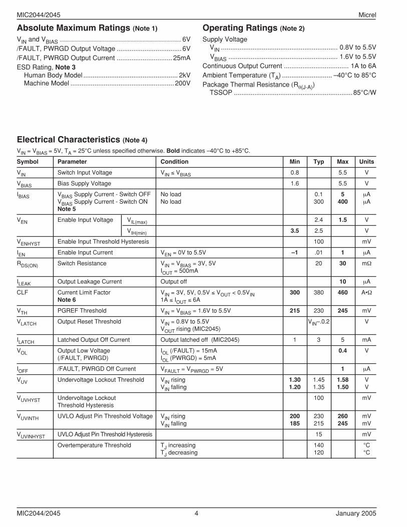
Absolute Maximum Ratings (Note 1)
VIN and VBIAS .................................................................................. 6V/FAULT, PWRGD Output Voltage ................................... 6V/FAULT, PWRGD Output Current .............................. 25mAESD Rating, Note 3
Human Body Model ................................................... 2kVMachine Model ........................................................ 200V
Operating Ratings (Note 2)
Supply VoltageVIN ............................................................... 0.8V to 5.5V
VBIAS ........................................................... 1.6V to 5.5VContinuous Output Current ................................... 1A to 6AAmbient Temperature (TA) ........................... –40°C to 85°CPackage Thermal Resistance (Rθ(J-A))
TSSOP ................................................................ 85°C/W
Electrical Characteristics (Note 4)
VIN = VBIAS = 5V, TA = 25°C unless specified otherwise. Bold indicates –40°C to +85°C.
Symbol Parameter Condition Min Typ Max Units
VIN Switch Input Voltage VIN ≤ VBIAS 0.8 5.5 V
VBIAS Bias Supply Voltage 1.6 5.5 V
IBIAS VBIAS Supply Current - Switch OFF No load 0.1 5 µAVBIAS Supply Current - Switch ON No load 300 400 µANote 5
VEN Enable Input Voltage VIL(max) 2.4 1.5 V
VIH(min) 3.5 2.5 V
VENHYST Enable Input Threshold Hysteresis 100 mV
IEN Enable Input Current VEN = 0V to 5.5V –1 .01 1 µA
RDS(ON) Switch Resistance VIN = VBIAS = 3V, 5V 20 30 mΩIOUT = 500mA
ILEAK Output Leakage Current Output off 10 µA
CLF Current Limit Factor VIN = 3V, 5V, 0.5V ≤ VOUT < 0.5VIN 300 380 460 A•ΩNote 6 1A ≤ IOUT ≤ 6A
VTH PGREF Threshold VIN = VBIAS = 1.6V to 5.5V 215 230 245 mV
VLATCH Output Reset Threshold VIN = 0.8V to 5.5V VIN–.0.2 VVOUT rising (MIC2045)
ILATCH Latched Output Off Current Output latched off (MIC2045) 1 3 5 mA
VOL Output Low Voltage IOL (/FAULT) = 15mA 0.4 V(/FAULT, PWRGD) IOL (PWRGD) = 5mA
IOFF /FAULT, PWRGD Off Current VFAULT = VPWRGD = 5V 1 µA
VUV Undervoltage Lockout Threshold VIN rising 1.30 1.45 1.58 VVIN falling 1.20 1.35 1.50 V
VUVHYST Undervoltage Lockout 100 mVThreshold Hysteresis
VUVINTH UVLO Adjust Pin Threshold Voltage VIN rising 200 230 260 mVVIN falling 185 215 245 mV
VUVINHYST UVLO Adjust Pin Threshold Hysteresis 15 mV
Overtemperature Threshold TJ increasing 140 °CTJ decreasing 120 °C
January 2005 5 MIC2044/2045
MIC2044/2045 Micrel
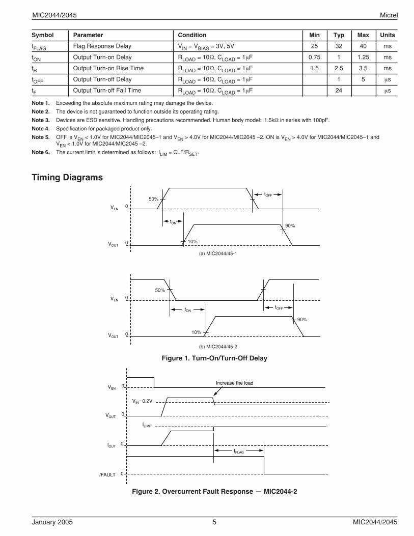
Symbol Parameter Condition Min Typ Max Units
tFLAG Flag Response Delay VIN = VBIAS = 3V, 5V 25 32 40 ms
tON Output Turn-on Delay RLOAD = 10Ω, CLOAD = 1µF 0.75 1 1.25 ms
tR Output Turn-on Rise Time RLOAD = 10Ω, CLOAD = 1µF 1.5 2.5 3.5 ms
tOFF Output Turn-off Delay RLOAD = 10Ω, CLOAD = 1µF 1 5 µs
tF Output Turn-off Fall Time RLOAD = 10Ω, CLOAD = 1µF 24 µs
Note 1. Exceeding the absolute maximum rating may damage the device.
Note 2. The device is not guaranteed to function outside its operating rating.
Note 3. Devices are ESD sensitive. Handling precautions recommended. Human body model: 1.5kΩ in series with 100pF.
Note 4. Specification for packaged product only.
Note 5. OFF is VEN < 1.0V for MIC2044/MIC2045–1 and VEN > 4.0V for MIC2044/MIC2045 –2. ON is VEN > 4.0V for MIC2044/MIC2045–1 andVEN < 1.0V for MIC2044/MIC2045 –2.
Note 6. The current limit is determined as follows: ILIM = CLF/RSET.
Timing Diagrams
50%
(a) MIC2044/45-1
(b) MIC2044/45-2
10%
90%
0VEN
tON
tOFF
0VOUT
50%
10%
90%
0VEN
tONtOFF
0VOUT
Figure 1. Turn-On/Turn-Off Delay
0VEN
ILIMIT
0VOUT
0IOUT
0/FAULT
tFLAG
VIN 0.2V
Increase the load
Figure 2. Overcurrent Fault Response — MIC2044-2
MIC2044/2045 Micrel
MIC2044/2045 6 January 2005
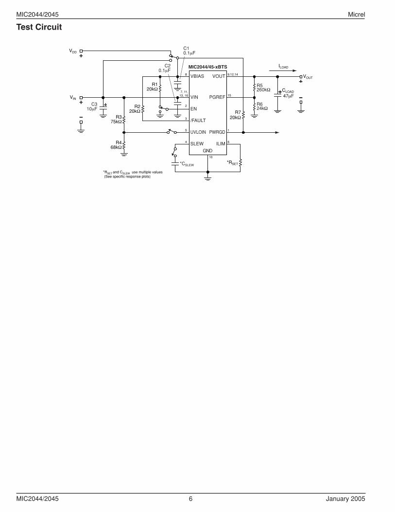
Test Circuit
7, 11,13, 16
8
2
3
5
4
15
9,12,14
1
6
*RSET
*RSET and CSLEW use multiple values (See specific response plots)
*CSLEW
C20.1µF
10
MIC2044/45-xBTS
VBIAS
VIN
EN
/FAULT
UVLOIN
SLEW
VOUT
PGREF
PWRGD
ILIM
GND
R220kΩ
R120kΩ
R5260kΩ
R624kΩ
CLOAD
47µF
VOUT
ILOAD
R720kΩ
C310µF
C10.1µF
VIN
VDD
R375kΩ
R468kΩ
January 2005 7 MIC2044/2045
MIC2044/2045 Micrel
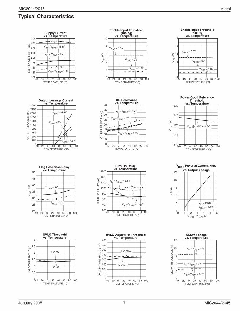
100
125
150
175
200
225
250
275
300
-40 -20 0 20 40 60 80 100
SU
PP
LY C
UR
RE
NT
(µ
A)
TEMPERATURE (°C)
Supply Currentvs. Temperature
VIN = VBIAS = 1.6V
VIN = VBIAS = 5.5V
VIN = VBIAS = 3V
0
1
2
3
4
5
-40 -20 0 20 40 60 80 100
V E
N (
V)
TEMPERATURE (°C)
Enable Input Threshold(Rising)
vs. Temperature
VBIAS = 5.5V
VBIAS = 3V
VBIAS = 1.6V
0
1
2
3
4
5
-40 -20 0 20 40 60 80 100
V E
N (
V)
TEMPERATURE (°C)
Enable Input Threshold(Falling)
vs. Temperature
VBIAS = 5.5V
VBIAS = 3V
VBIAS = 1.6V
0
250
500
750
1000
1250
1500
1750
2000
2250
2500
-40 -20 0 20 40 60 80 100
OU
TP
UT
LE
AK
AG
E (
nA)
TEMPERATURE (°C)
Output Leakage Currentvs. Temperature
VBIAS = 5.5V
VBIAS = 3V
VBIAS = 1.6V0
5
10
15
20
25
30
35
40
-40 -20 0 20 40 60 80 100
ON
RE
SIS
TA
NC
E (
mΩ
)
TEMPERATURE (°C)
ON Resistancevs. Temperature
VIN = VBIAS = 1.6V
VIN = VBIAS = 3V
VIN = VBIAS = 5.5V
20
25
30
35
40
45
50
-40 -20 0 20 40 60 80 100
T F
LAG
(m
s)
TEMPERATURE (°C)
Flag Response Delayvs. Temperature
TFLAG = 3V
TFLAG = 5V
200
400
600
800
1000
1200
1400
1600
-40 -20 0 20 40 60 80 100
TU
RN
ON
DE
LAY
(µ
s)
TEMPERATURE (°C)
Turn On Delayvs. Temperature
VIN = VBIAS = 5.5V
VIN = VBIAS = 3V
VIN = VBIAS = 1.6V
0
5
10
15
20
25
0 1 2 3 4 5 6
I R (
mA
)
V OUT –V BIAS (V)
VBIAS Reverse Current Flowvs. Output Voltage
VIN = GNDVBIAS = 1.6V
Typical Characteristics
0
0.5
1
1.5
2
2.5
3
-40 -20 0 20 40 60 80 100
UV
LO T
HR
ES
HO
LD (
V)
TEMPERATURE (°C)
UVLO Thresholdvs. Temperature
UVLO+
UVLO–
0
50
100
150
200
250
300
350
400
-40 -20 0 20 40 60 80 100
UV
LOIN
TH
RE
SH
OLD
(m
V)
TEMPERATURE (°C)
UVLO Adjust Pin Thresholdvs. Temperature
UVLOIN+
UVLOIN–
0
5
10
15
20
25
-40 -20 0 20 40 60 80 100
SLE
W P
IN V
OLT
AG
E (
V)
TEMPERATURE (°C)
SLEW Voltagevs. Temperature
VIN = VBIAS = 1.6V
VIN = VBIAS = 5V
VIN = VBIAS = 3V
210
215
220
225
230
-40 -20 0 20 40 60 80 100
V T
H (
mV
)
TEMPERATURE (°C)
Power-Good ReferenceThreshold
vs. Temperature
VTH @ 1.6V to 5.5V
MIC2044/2045 Micrel
MIC2044/2045 8 January 2005
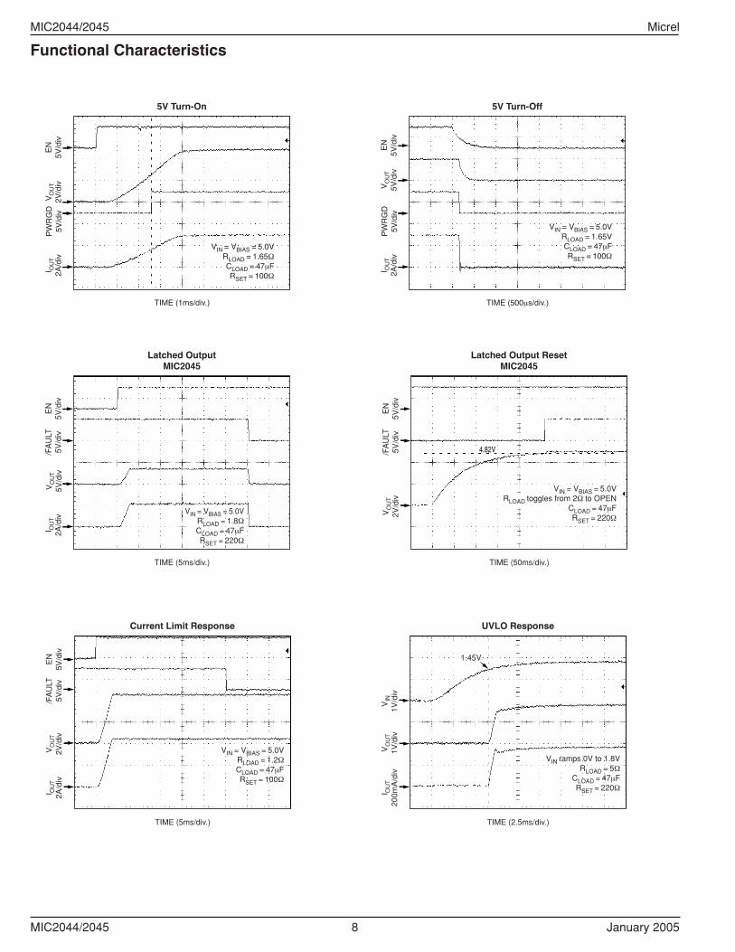
Functional Characteristics
!
" #$%&
!
" #$%
I OU
T2A
/div
VO
UT
5V/d
iv/F
AU
LT5V
/div
EN
5V/d
iv
VIN = VBIAS = 5.0VRLOAD = 1.8ΩCLOAD = 47µFRSET = 220Ω
Latched OutputMIC2045
TIME (5ms/div.)
VO
UT
2V/d
iv/F
AU
LT5V
/div
EN
5V/d
iv
VIN = VBIAS = 5.0VRLOAD toggles from 2Ω to OPEN
CLOAD = 47µFRSET = 220Ω
4.82V
Latched Output ResetMIC2045
TIME (50ms/div.)
I OU
T20
0mA
/div
VIN
1V/d
ivV
OU
T1V
/div
VIN ramps 0V to 1.8VRLOAD = 5Ω
CLOAD = 47µFRSET = 220Ω
UVLO Response
TIME (2.5ms/div.)
1.45V
I OU
T2A
/div
/FA
ULT
5V/d
ivE
N5V
/div
VO
UT
2V/d
iv
VIN = VBIAS = 5.0VRLOAD = 1.2ΩCLOAD = 47µFRSET = 100Ω
Current Limit Response
TIME (5ms/div.)
January 2005 9 MIC2044/2045
MIC2044/2045 Micrel
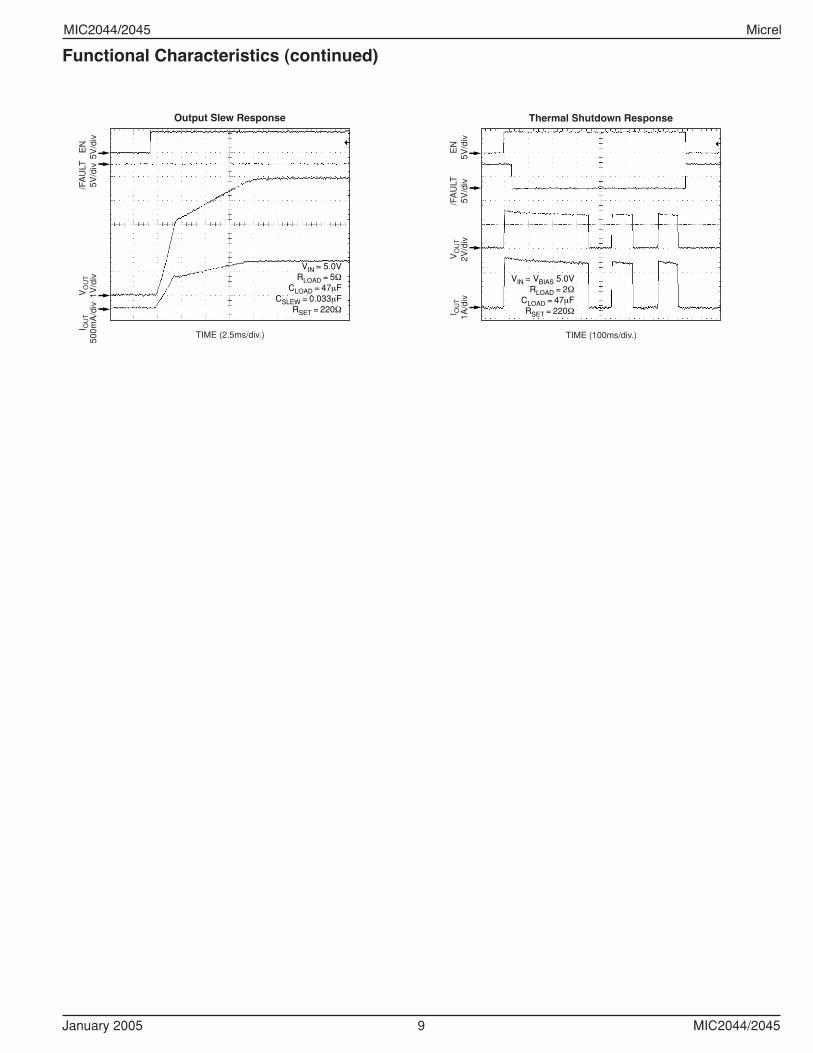
Functional Characteristics (continued)V
OU
T1V
/div
/FA
ULT
5V/d
ivE
N5V
/div
I OU
T50
0mA
/div
VIN = 5.0VRLOAD = 5Ω
CLOAD = 47µFCSLEW = 0.033µF
RSET = 220Ω
Output Slew Response
TIME (2.5ms/div.)
VO
UT
2V/d
iv/F
AU
LT5V
/div
EN
5V/d
ivI O
UT
1A/d
iv
VIN = VBIAS 5.0VRLOAD = 2Ω
CLOAD = 47µFRSET = 220Ω
Thermal Shutdown Response
TIME (100ms/div.)
MIC2044/2045 Micrel
MIC2044/2045 10 January 2005
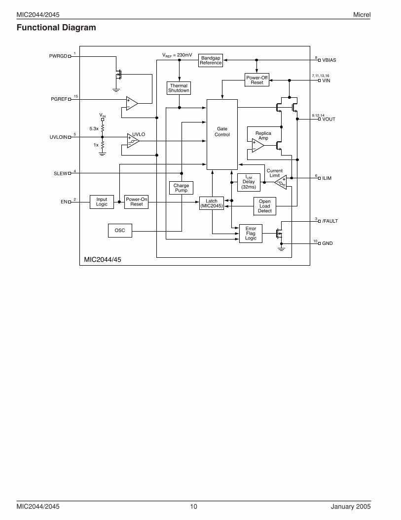
Functional Diagram
MIC2044/45
BandgapReference
OSC
UVLO
5.3x
1x
VREF = 230mV
CurrentLimit
ReplicaAmp
VIN
ILIM6
VOUT9,12,14
VBIAS8
VIN7,11,13,16
/FAULT3
GND10
Gate
ControlUVLOIN
5
SLEW4
EN2
PGREF15
OpenLoadDetect
ILIMDelay(32ms)
PWRGD1
ErrorFlagLogic
Power-OnReset
InputLogic
Latch(MIC2045)
ChargePump
ThermalShutdown
Power-OffReset
January 2005 11 MIC2044/2045
MIC2044/2045 Micrel
Functional DescriptionThe MIC2044 and MIC2045 are high-side N-Channel switchesequipped with programmable current limit up to 6A for use ingeneral purpose power distribution applications. The switches,available with active-high or active-low enable inputs, provideoutput slew-rate control and circuit protection via thermalshutdown and an optional output latch during overcurrentconditions.
Input and Output
VBIAS supplies power to the internal circuitry of the switchand must be present for the switch to operate. VIN is con-nected to the drain of the output MOSFET and sources powerto the switched load. VIN must be less than or equal to VBIAS.VOUT is the source terminal of the output MOSFET andattaches to the load. In a typical circuit, current flows from VINto VOUT toward the load. If VOUT is greater than VIN, currentwill flow from VOUT to VIN since the switch is bi-directionalwhen the device is enabled. When disabled (OFF), the switchwill block current flow from either direction.
Enable Input
Enable, the ON/OFF control for the output switch, is a digitalinput available as an active-high (–1) or active-low (–2)signal. The EN pin, referenced to approximately 0.5 × VBIAS,must be driven to a clearly defined logic high or logic low.Failure to observe this requirement, or allowing EN to float,will cause the MIC2044/45 to exhibit unpredictable behavior.EN should not be allowed to go negative with respect toground, nor allowed to exceed VBIAS. Failure to adhere tothese conditions may result in damage to the device.
Undervoltage Lockout
When the switch is enabled, undervoltage lockout (UVLO)monitors the input voltage, VIN, and prevents the outputMOSFET from turning on until VIN exceeds a predeterminedlevel, nominally set at 1.45V. The UVLO threshold is adjust-able and can be varied by applying an external resistor dividerto the UVLOIN pin from VIN to GND. The resistive dividernetwork is required when the input voltage is below 1.5V. TheUVLO threshold is internally preset to 1.45V if the UVLOINpin is left open. See “Applications Information.”
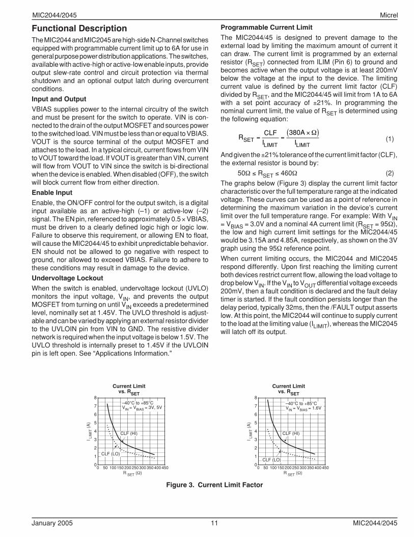
Programmable Current Limit
The MIC2044/45 is designed to prevent damage to theexternal load by limiting the maximum amount of current itcan draw. The current limit is programmed by an externalresistor (RSET) connected from ILIM (Pin 6) to ground andbecomes active when the output voltage is at least 200mVbelow the voltage at the input to the device. The limitingcurrent value is defined by the current limit factor (CLF)divided by RSET, and the MIC2044/45 will limit from 1A to 6Awith a set point accuracy of ±21%. In programming thenominal current limit, the value of RSET is determined usingthe following equation:
RCLF
I
380A
ISETLIMIT LIMIT
= =× Ω( )
(1)
And given the ±21% tolerance of the current limit factor (CLF),the external resistor is bound by:
50Ω ≤ RSET ≤ 460Ω (2)
The graphs below (Figure 3) display the current limit factorcharacteristic over the full temperature range at the indicatedvoltage. These curves can be used as a point of reference indetermining the maximum variation in the device’s currentlimit over the full temperature range. For example: With VIN= VBIAS = 3.0V and a nominal 4A current limit (RSET = 95Ω),the low and high current limit settings for the MIC2044/45would be 3.15A and 4.85A, respectively, as shown on the 3Vgraph using the 95Ω reference point.
When current limiting occurs, the MIC2044 and MIC2045respond differently. Upon first reaching the limiting currentboth devices restrict current flow, allowing the load voltage todrop below VIN. If the VIN to VOUT differential voltage exceeds200mV, then a fault condition is declared and the fault delaytimer is started. If the fault condition persists longer than thedelay period, typically 32ms, then the /FAULT output assertslow. At this point, the MIC2044 will continue to supply currentto the load at the limiting value (ILIMIT), whereas the MIC2045will latch off its output.
0
1
2
3
4
5
6
7
8
0 50 100 150 200 250 300 350 400 450
I LIM
IT (
A)
R SET (Ω)
Current Limitvs. RSET
–40°C to +85°CVIN = VBIAS = 3V, 5V
CLF (LO)
CLF (HI)
0
1
2
3
4
5
6
7
8
0 50 100 150 200 250 300 350 400 450
I LIM
IT (
A)
R SET (Ω)
Current Limitvs. RSET
–40°C to +85°CVIN = VBIAS = 1.6V
CLF (LO)
CLF (HI)
Figure 3. Current Limit Factor
MIC2044/2045 Micrel
MIC2044/2045 12 January 2005
/FAULT
The /FAULT signal is an N-Channel, open-drain MOSFEToutput. An external pull-up resistor tied to a maximum 6V railis required for the /FAULT pin. The /FAULT pin is asserted(active-low) when either an overcurrent or thermal shutdowncondition occurs. During a hot insert of a PCB or when turningon into a highly capacitive load, the resulting high transientinrush current may exceed the current limit threshold of theMIC2044/45. In the case where an overcurrent conditionoccurs, /FAULT will assert only after the flag delay time haselapsed, typically 32ms. This ensures that /FAULT is as-serted only upon valid overcurrent conditions and that nui-sance error reporting is prevented.
Thermal Shutdown
For the MIC2044, thermal shutdown is employed to protectthe device from damage should the die temperature exceedsafe margins due to a short circuit or an excessive load.Thermal shutdown shuts off the output MOSFET and assertsthe /FAULT output if the die temperature exceeds 140°C.The MIC2044 automatically resets its output and resumessupplying current to the load when the die temperature dropsto 120°C. If the fault is still present, the MIC2044 will quicklyre-heat and shut down again. This process of turningON-OFF-ON is called thermal cycling and will continue aslong as the power switch is enabled while the fault orexcessive load is present.
Depending on PCB layout (including thermal considerationssuch as heat sinking), package, and ambient temperature, itmay take several hundred milliseconds from the incidence ofthe fault to the output MOSFET being shut off.
Circuit Breaker Function (MIC2045)
The MIC2045 is designed to shut off all power to the loadwhen a fault condition occurs, just as a circuit breaker woulddo. In this case, a fault condition is deemed to be anytime theoutput current exceeds the current limit for more than the flagdelay period, nominally 32ms. Once the output shuts off, itremains off until either the fault load is removed from VOUTor the EN input is cycled ON-OFF-ON. If the fault is stillpresent after EN has been cycled, the MIC2045 will againshut off all power to the load after 32ms. Once the fault hasbeen removed, then normal operation will resume.
Open Load Detection
The MIC2045 will automatically reset its output when the faultload is cleared. This is accomplished by applying a smallcurrent to VOUT and watching for the voltage at VOUT to riseto within 200mV of VIN. This current is supplied by an internalresistor connected to VIN and is connected to VOUT whenMIC2045 latches off.
Power-Good Detection
The MIC2044/45 can detect when the output voltage is aboveor below a preset threshold that is monitored by a comparatorat the PGREF input. The PWRGD signal is an N-Channelopen-drain MOSFET output and an external pull-up resistorup to a 6V maximum rail is required for the PWRGD pin.Whenever the voltage at the PGREF pin exceeds its thresh-old (VTH), typically 230mV, the PWRGD output is asserted.Using the typical applications circuit from page 1 that switches3.3V as an example, the output voltage threshold determin-ing “power is good” is calculated by the following equation:
V V 1R2R3OUT(GOOD) TH= × +
(3)
In substituting the resistor values of the circuit and the typicalPGREF threshold, the resulting VOUT(GOOD) is calculated as3.0V for this 3.3V switching application.
SLEW
The MIC2044/45’s output rise time is controlled at turn-on toa minimum of 1.5ms and is controlled by an internal slew-ratelimiting circuit. A slew-rate adjustment control pin is availablefor applications requiring slower rise times. By placing acapacitor between SLEW and ground, longer rise times canbe achieved. For further detail, see the “Applications Informa-tion” section.
January 2005 13 MIC2044/2045
MIC2044/2045 Micrel
Applications InformationInput and OutputSupply Bypass Filtering
The need for input supply bypass is brought about due toseveral factors, most notably the input/output inductancealong the power path, operating current and current limit, andoutput capacitance. A 0.1µF to 0.47µF bypass capacitorpositioned very close to the VIN pin to GND of the device isstrongly recommended to filter high frequency oscillationsdue to inductance. Also, a sufficient bypass capacitor posi-tioned close to the input source to the switch is stronglyadvised in order to suppress supply transient spikes and tolimit input voltage droop. Inrush current increases with largeroutput capacitance, thus the minimum value of this capacitorwill require experimental determination for the intended appli-cation and design. A good starting point is a capacitorbetween 4.7µF to 15µF. Without these bypass capacitors, anextreme overload condition such as a short circuit, or a largecapacitive load, may cause either the input supply to exceedthe maximum rating of 6V and possibly cause damage to theinternal control circuitry or allow the input supply to droop andfall out of regulation and/or below the minimum operatingvoltage of the device.Output Capacitance
When the MIC2044 die exceeds the overtemperature thresh-old of approximately 140°C, the device can enter into athermal shutdown mode if the die temperature falls below120°C and then rises above 140°C in a continuous cycle.With VOUT cycling on and off, the MIC2044 will reset the/FAULT while in an overtemperature fault condition if VOUT isallowed to swing below ground. The inductance present atthe output must be neutralized by capacitance in order toensure that the output does not fall below ground. In order tocounter the board parasitic inductance and the inductance ofrelatively short-length power cable (≤ 1ft., 16 - 20 gauge wire),a minimum output capacitance of 22µF is strongly recom-mended and should be placed close to the VOUT pin of theMIC2044. For applications that use more than a foot of cable,an additional 10µF/ft. is recommended.Reverse Current Blocking
The MIC2044/45 provides reverse current flow blockingthrough the output MOSFET if the voltage at VOUT is greaterthan VIN when the device is disabled. The VBIAS supply hasa limited reverse current flow if the voltage at VOUT is pulledabove VBIAS when the device is disabled. A graph of theVBIAS reverse current flow is shown in the “FunctionalCharacteristics” section. The reverse current for VBIAS canbe completely blocked by inserting a Schottky diode from theVBIAS pin (cathode) to the supply (anode). However, theminimum voltage of 1.6V must be supplied to VBIAS afteraccounting for the voltage drop across the diode.
Output Slew-Rate Adjustment
The output slew-rate for the MIC2044/45 can be slowed downby the use of a capacitor (16V rating, minimum; 25V sug-gested) between SLEW and GND. The slew-rate controlcircuitry is independent of the load capacitance and exhibits
a non-linear response. See the “Functional Characteristics”section. Table 1 shows the rise time for various standardcapacitor values. Additionally, the output turn-on time mustbe less than the nominal flag delay of 32ms in order to avoidnuisance tripping of the /FAULT output. This limit is imposedby the current limiting circuitry which monitors the(VIN – VOUT) differential voltage and concludes a faultcondition is present if the differential voltage exceeds 200mVfor more than the flag delay period. For the MIC2045, the/FAULT will assert and the output will latch off if the output isnot within 200mV of the input before the flag delay times out.When using the active-low (–2) option with the EN input tiedto ground, slew control is functional during initial start-up butdoes not function upon resetting the input power to thedevice. In order for the SLEW control to operate duringconsecutive system restarts, the EN pin must reset (toggleOFF to ON).
UVLO Threshold Setting With Low Input Voltages
When the switching voltage is below 1.6V, the device’sstandard UVLO threshold (1.45V nominal) will hinder theoutput MOSFET in switching VIN to VOUT. In this case, theuse of the UVLOIN pin is required to override the standardUVLO threshold and set a new, lower threshold for the lowerinput voltage. An external resistive divider network con-nected at the UVLOIN pin is used to set the new threshold.Due to the ratio of the internal components, the total seriesresistance of the external resistive divider should not exceed200kΩ. The circuit shown in Figure 4 illustrates an applicationthat switches 0.8V while the device is powered from aseparate 2.5V power supply. The UVLO threshold is set bythe following equation.
V 0.23V 1R2R3UVTH = × +
(4)
In substituting the resistor values from Figure 4, the resultingUVLO threshold (VUVTH) is calculated as 0.6V for this 0.8Vswitching application. When using the UVLOIN pin to set anew UVLO threshold, an optional 0.1µF to 1.0µF capacitorfrom UVLOIN to GND may be used as a glitch filter in orderto avoid nuisance tripping of the UVLO threshold. If theUVLOIN pin is not in use, this pin should be left open(floating). The use of a pull-down resistor to ground will offsetthe ratio of the internal resistive divider to this pin resulting ina shift in the UVLO threshold. To bypass (disable) UVLO,connect the UVLOIN pin directly to the VIN pin of theMIC2044/45.
Conditions: VIN = VBIAS = 5V/3VCLOAD = 47µF; ILOAD = 1A
CSLEW (µF) Rise Time (ms)
5V 3V
0.02 4.4 6.6
0.033 7.5 11.25
0.047 11 16
0.1 24 31.5
Table 1. Typical Output Rise Time for Various CSLEW(VIN = 5V, 3V)
MIC2044/2045 Micrel
MIC2044/2045 14 January 2005
!
!"
!"
$
!
%&%'()*'+*'%&,()-
!
"
!
"
!
.'/0
)) +%,- 1 2 3*-' 4/ /5'/6,())7 '%/8 '.&/'9/6
)) +%,- 1 2 3*-' 4/ /5'/6,())7 '%/8 '.&/'9/6
,8/6:.)'(&/ .;!.*' <
*'+*' .=/6>..8 <
Figure 4. Lower UVLO Setting
Power Dissipation
Power dissipation depends on several factors such as theload, PCB layout, ambient temperature, and package type.The following equations can be used to calculate powerdissipation and die temperature.
Calculation of power dissipation can be accomplished by thefollowing equation:
PD = RDS(on) × (IOUT)2 (5)
To relate this to junction temperature, the following equationcan be used:
TJ = PD × R(θJ-A) + TA (6)
where TJ = junction temperature, TA = ambient temperatureand Rθ(J-A) is the thermal resistance of the package.
Printed Circuit Board Hot Plug
The MIC2044/45 are ideal inrush current limiting powerswitches suitable for hot plug applications. Due to the inte-grated charge pump, the MIC2044/45 present a high imped-ance when in the off state and the device slowly becomes alow impedance as it turns on. This effectively isolates powersupplies from highly capacitive loads by reducing inrushcurrent during hot plug events. This same feature also can beused for soft-start requirements.
PCB Layout Recommendations
The MIC2044 and MIC2045 have very low on-resistance,typically 20mΩ, and the switches can provide up to 6A ofcontinuous output current. Under heavy loads, the switchedcurrent may cause the devices to heat up considerably. Thefollowing list contains some useful suggestions for PCBlayout design of the MIC2044/45 in order to prevent the diefrom overheating under normal operating conditions. 1. Micrel Semiconductor does not assume responsibility for the use of
this program tool in the event that any PCB assembled, tested,produced, and/or manufactured becomes damaged and/or causes anydegradation of system performance or damage to any systemcomponents in which the aforementioned PCB is included.
1. Supply additional copper area under the deviceto remove heat away from the IC.
See “Application Hint 17” for a general guidelinein calculating the suggested area.
2. Provide additional pad area on the corner pins ofthe MIC2044/45 IC for heat distribution.
3. Tie the common power pins (VIN = pins 7, 11,13, 16 and VOUT = pins 9, 12, 14) together in amanner such that the traces entering andleaving the device have a uniform width suffi-cient for the application’s current requirementsplus added margin (25% minimum recom-mended).
Ex: For 4A maximum current, design traces for5A capability.
4. For PCB trace width calculation, there arenumerous calculator programs available on theinternet and elsewhere. As a general rule ofthumb, 15-20 mils width for every 1A of currentwhen using 1oz. copper. However, the tracewidth calculators often take into account maxi-mum temperature increase constraints, as wellas layer arrangement, in determining the PCBtrace widths. As a reference, the following link issuggested for trial tests in PCB trace widthcalculations.1
http://www.aracnet.com/cgi-usr/gpatrick/trace.pl
January 2005 15 MIC2044/2045
MIC2044/2045 Micrel
Package Information
Rev. 01
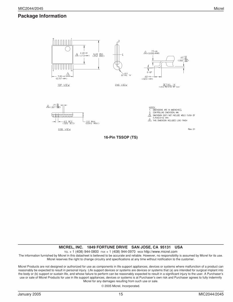
16-Pin TSSOP (TS)
MICREL, INC. 1849 FORTUNE DRIVE SAN JOSE, CA 95131 USATEL + 1 (408) 944-0800 FAX + 1 (408) 944-0970 WEB http://www.micrel.com
The information furnished by Micrel in this datasheet is believed to be accurate and reliable. However, no responsibility is assumed by Micrel for its use.Micrel reserves the right to change circuitry and specifications at any time without notification to the customer.
Micrel Products are not designed or authorized for use as components in life support appliances, devices or systems where malfunction of a product canreasonably be expected to result in personal injury. Life support devices or systems are devices or systems that (a) are intended for surgical implant intothe body or (b) support or sustain life, and whose failure to perform can be reasonably expected to result in a significant injury to the user. A Purchaser’suse or sale of Micrel Products for use in life support appliances, devices or systems is at Purchaser’s own risk and Purchaser agrees to fully indemnify
Micrel for any damages resulting from such use or sale.
© 2005 Micrel, Incorporated.