Methods of photoelectrode characterization with high...
24
Energy & Environmental Science www.rsc.org/ees ISSN 1754-5692 SPECIAL COLLECTION Editorial by Eric Miller, with contributions from Ager et al., Fabian et al., Coridan et al., Smith et al. and Esposito et al. Photoelectrochemical Water Splitting Volume 8 Number 10 October 2015 Pages 2799–3050 Published on 19 June 2015. Downloaded on 29/10/2015 17:26:34. View Article Online View Journal | View Issue
Transcript of Methods of photoelectrode characterization with high...

Energy &Environmental Sciencewww.rsc.org/ees
ISSN 1754-5692
SPECIAL COLLECTIONEditorial by Eric Miller, with contributions from Ager et al., Fabian et al., Coridan et al., Smith et al. and Esposito et al.Photoelectrochemical Water Splitting
Volume 8 Number 10 October 2015 Pages 2799–3050
Publ
ishe
d on
19
June
201
5. D
ownl
oade
d on
29/
10/2
015
17:2
6:34
.
View Article OnlineView Journal | View Issue

This journal is©The Royal Society of Chemistry 2015 Energy Environ. Sci., 2015, 8, 2863--2885 | 2863
Cite this: Energy Environ. Sci.,
2015, 8, 2863
Methods of photoelectrode characterization withhigh spatial and temporal resolution
Daniel V. Esposito,*ab Jason B. Baxter,c Jimmy John,d Nathan S. Lewis,de
Thomas P. Moffat,b Tadashi Ogitsu,f Glen D. O’Neil,a Tuan Anh Pham,f
A. Alec Talin,g Jesus M. Velazquezde and Brandon C. Woodf
Materials and photoelectrode architectures that are highly efficient, extremely stable, and made from low cost
materials are required for commercially viable photoelectrochemical (PEC) water-splitting technology. A key
challenge is the heterogeneous nature of real-world materials, which often possess spatial variation in their
crystal structure, morphology, and/or composition at the nano-, micro-, or macro-scale. Different structures
and compositions can have vastly different properties and can therefore strongly influence the overall
performance of the photoelectrode through complex structure–property relationships. A complete under-
standing of photoelectrode materials would also involve elucidation of processes such as carrier collection and
electrochemical charge transfer that occur at very fast time scales. We present herein an overview of a broad
suite of experimental and computational tools that can be used to define the structure–property relationships of
photoelectrode materials at small dimensions and on fast time scales. A major focus is on in situ scanning-
probe measurement (SPM) techniques that possess the ability to measure differences in optical, electronic,
catalytic, and physical properties with nano- or micro-scale spatial resolution. In situ ultrafast spectroscopic
techniques, used to probe carrier dynamics involved with processes such as carrier generation, recombination,
and interfacial charge transport, are also discussed. Complementing all of these experimental techniques are
computational atomistic modeling tools, which can be invaluable for interpreting experimental results, aiding in
materials discovery, and interrogating PEC processes at length and time scales not currently accessible by
experiment. In addition to reviewing the basic capabilities of these experimental and computational techniques,
we highlight key opportunities and limitations of applying these tools for the development of PEC materials.
Broader contextGlobal energy demands are currently around 14 TW, and are forecasted to double by 2050. To date, this energy has been derived from non-renewable fossilfuels, but environmental issues such as climate change have created an urgent need to transition to carbon-free energy sources. Abundant and renewable solarenergy is one of the most promising means of meeting society’s energy demands in a sustainable manner, but the intermittent nature of sunlight createssignificant challenges to achieving high market penetration with conventional photovoltaic technology alone. Photoelectrochemical (PEC) water-splitting canconvert sunlight into storable chemical energy in the form of hydrogen gas (H2), but commercialization of this technology has been hindered by the stability,efficiency, and cost of photoelectrodes. In order to accelerate the development of photoelectrode materials, which are often highly heterogeneous in nature andinherently involve phenomena at multiple time scales, a deeper understanding of PEC processes at small length scales and fast time scales is essential. Thisarticle provides a review of a combination of in situ experimental techniques and modeling tools that are well-suited for such studies.
1. Introduction
The generation of hydrogen through photoelectrochemical(PEC) water splitting, whereby light is used to electrochemicallysplit water into molecular hydrogen and oxygen, is a promisingapproach to producing storable, scalable, and carbon-freerenewable energy.1–4 However, no PEC system has been demon-strated to date that can meet the efficiency, stability, and costtargets5 needed for an economically viable PEC technology.6
One of the major barriers to commercialization is the lack ofsuitable materials to be used in photoelectrodes,2,4 the ‘‘engines’’
a Department of Chemical Engineering, Columbia University in the City of New York,
New York, NY, 10027, USA. E-mail: [email protected]; Tel: +1-212-854-2648b National Institute of Standards and Technology, Gaithersburg, MD, 20899, USAc Department of Chemical and Biological Engineering, Drexel University,
Philadelphia, PA, 19104, USAd Division of Chemistry and Chemical Engineering, California Institute of
Technology, Pasadena, CA, 91125, USAe Joint Center for Artificial Photosynthesis, California Institute of Technology,
Pasadena, CA, 91125, USAf Quantum Simulations Group, Lawrence Livermore National Laboratory, Livermore,
CA, 94550, USAg Sandia National Laboratories, Livermore, CA, 94551, USA
Received 13th March 2015,Accepted 18th June 2015
DOI: 10.1039/c5ee00835b
www.rsc.org/ees
Energy &EnvironmentalScience
REVIEW
Publ
ishe
d on
19
June
201
5. D
ownl
oade
d on
29/
10/2
015
17:2
6:34
. View Article Online

2864 | Energy Environ. Sci., 2015, 8, 2863--2885 This journal is©The Royal Society of Chemistry 2015
of PEC devices that are responsible for absorbing light andusing the resulting potential energy difference to drivethe water splitting reaction. To perform these functions withhigh efficiency and durability, photoelectrode materials andarchitectures are needed that are extremely stable, absorb asignificant portion of the solar spectrum, possess high catalyticactivity for the hydrogen- and oxygen-evolution reactions (HERand OER, respectively), produce a large photovoltage, exhibithigh carrier lifetimes, and are predominantly comprised ofearth-abundant elements.
Finding a single material or combination of materials thatare capable of meeting all of these requirements is a dauntingtask. Ever since Fujishima and Honda first demonstrated PECwater splitting with TiO2 in 1972,7 many different classes ofsemiconductors have been explored as photoelectrode absorbers,including metal oxides, chalcopyrites, chalcogenides, group III–Vsemiconductors, group V semiconductors (Si), and more.3,8–10
None of the materials investigated thus far have been capable ofmeeting all of the aforementioned photoelectrode requirementsby themselves. However, the opportunity to discover a suitablephotoelectrode material or combination of materials is tremen-dous when one considers that there are E800 two-componentand E104 tri-component combinations of earth-abundantelements,11 and a nearly infinite number of atomic arrangements.The use of composite photoelectrode architectures containing acombination of semiconducting absorber(s), metallic catalysts,and protective insulating layers increases the number of composi-tional permutations even further.
Due to the sheer number of candidate materials, high-throughput experimental12–16 and computational17,18 screeningmethods naturally lend themselves as useful tools for identifyingpromising photoelectrode materials. However, the developmentprocess only begins once a new, promising material compositionhas been identified. Subsequently, realizing the full potential ofa material for PEC water splitting requires rigorous downstreamoptimization and experimentation. Through different synthesismethods and conditions, many parameters can be varied tooptimize a material’s performance, including crystal phases andorientations, composition, morphology, substrate and co-catalystselection, dopant distribution, defect engineering, and more. All ofthese factors can have a huge impact on the overall performance ofa photoelectrode. Unfortunately, precise and independent controlof these factors is generally not possible. For example, manymaterials are highly heterogeneous in nature, possessing variationin crystallinity, composition, and/or morphology at the nano-,micro-, and/or macro-scales. Heterogeneous photoelectrodes oftenresult in macro-scale performance that is a complex convolution ofthe local performance associated with different compositions,structures, and morphologies. Additionally, most fundamentalprocesses involved with PEC energy conversion are dynamicprocesses taking place over timescales typically ranging fromfemtoseconds (fs) to microseconds (ms).19
Deconvolving the structure–property relationships in situwith high spatial and temporal resolution is thus importantfor obtaining an advanced understanding of photoelectrodebehavior and then using that knowledge to design better
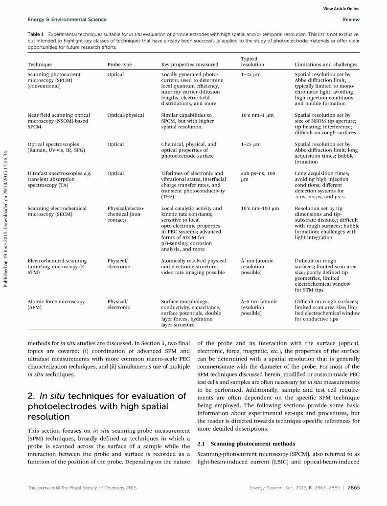
photoelectrodes. The study of photoelectrodes in situ and underreal or simulated operating conditions in an electrochemicalenvironment is especially important because the properties andcharacteristics of a photoelectrode are often intimately coupledto the properties of the liquid-phase electrolyte.20,21 As describedin more detail in the review article by Smith et al.,22 the electrolytecan strongly affect the chemical and electronic properties of thesurface and space-charge layer of the photoelectrode, andtherefore influence catalytic, charge transport, and corrosionprocesses. Ex situ techniques performed in atmosphere orvacuum can also provide important and complementary infor-mation about a photoelectrode material, but cannot substitutefor viewing the true physical and chemical state of the materialin a photoelectrochemical environment. Fortunately, manyexperimental and computational tools are well-suited for themeasurement of spatially varying properties and/or ultrafastcarrier dynamics in a PEC environment. Table 1 lists the majortypes of experimental techniques that are suitable for in situanalysis of photoelectrodes with high spatial and/or temporalresolution. Table 2, to be discussed in Section 4, providessimilar information for atomistic computational tools.
Table 1 can be split into two broad types of techniques: scanningprobe measurement (SPM) techniques used for achieving highspatial resolution, and pump–probe type spectroscopic techniquesused for monitoring ultrafast processes with high temporalresolution. Several major uses and benefits of in situ techniqueswith high spatial and/or temporal resolution are as follows:
(i) Diagnostic – by investigating the spatial variation inproperties or performance of a photoelectrode, SPM techniquescan be used to locate poorly performing ‘‘cold spots’’ and highlyperforming ‘‘hot spots’’ on the photoelectrode. Using additionalin situ or ex situ characterization, the structural and/or composi-tional variation that gives rise to the regions of anomalousperformance can then be identified. Likewise, fast events likecharge-carrier recombination and interfacial charge transfer canbe studied to complement SPM techniques by identifying rate-limiting processes. This information can be an important sourceof feedback for optimization of the design of the photoelectrode.
(ii) Mechanistic – carefully-designed SPM and/or ultrafastspectroscopy measurements can provide a deeper understandingof physical, opto-electronic, and catalytic PEC processes, allowingfor further refinement of the computational models used foridentifying even better photoelectrode materials.
(iii) Screening – many in situ SPM techniques are well suitedfor rapid measurement of the properties or performance of largearrays of (typically) millimeter-sized samples for the purpose ofhigh-throughput screening. Generally, high spatial resolutionand ultrafast spectroscopy are not needed in these studies, andthe reader is referred to other literature on the topic.12,15,16,23–28
The remainder of this paper provides an overview of in situSPM techniques (Section 2), ultrafast spectroscopy techniques(Section 3), and computational tools (Section 4) that have beenused, or have the potential to be used, for in situ investigationphotoelectrodes with high spatial and/or temporal resolution.In addition to describing the basic principles behind each classof techniques, the opportunities and challenges for using these
Review Energy & Environmental Science
Publ
ishe
d on
19
June
201
5. D
ownl
oade
d on
29/
10/2
015
17:2
6:34
. View Article Online
This journal is©The Royal Society of Chemistry 2015 Energy Environ. Sci., 2015, 8, 2863--2885 | 2865
methods for in situ studies are discussed. In Section 5, two finaltopics are covered: (i) coordination of advanced SPM andultrafast measurements with more common macro-scale PECcharacterization techniques, and (ii) simultaneous use of multiplein situ techniques.
2. In situ techniques for evaluation ofphotoelectrodes with high spatialresolution
This section focuses on in situ scanning-probe measurement(SPM) techniques, broadly defined as techniques in which aprobe is scanned across the surface of a sample while theinteraction between the probe and surface is recorded as afunction of the position of the probe. Depending on the nature
of the probe and its interaction with the surface (optical,electronic, force, magnetic, etc.), the properties of the surfacecan be determined with a spatial resolution that is generallycommensurate with the diameter of the probe. For most of theSPM techniques discussed herein, modified or custom-made PECtest cells and samples are often necessary for in situ measurementsto be performed. Additionally, sample and test cell require-ments are often dependent on the specific SPM techniquebeing employed. The following sections provide some basicinformation about experimental set-ups and procedures, butthe reader is directed towards technique-specific references formore detailed descriptions.
2.1 Scanning photocurrent methods
Scanning-photocurrent microscopy (SPCM), also referred to aslight-beam-induced current (LBIC) and optical-beam-induced
Table 1 Experimental techniques suitable for in situ evaluation of photoelectrodes with high spatial and/or temporal resolution. This list is not exclusive,but intended to highlight key classes of techniques that have already been successfully applied to the study of photoelectrode materials or offer clearopportunities for future research efforts
Technique Probe type Key properties measuredTypicalresolution Limitations and challenges
Scanning photocurrentmicroscopy (SPCM)(conventional)
Optical Locally generated photo-current; used to determinelocal quantum efficiency,minority carrier diffusionlengths, electric fielddistributions, and more
1–25 mm Spatial resolution set byAbbe diffraction limit;typically limited to mono-chromatic light; avoidinghigh injection conditionsand bubble formation
Near field scanning opticalmicroscopy (NSOM)-basedSPCM
Optical/physical Similar capabilities toSPCM, but with higherspatial resolution.
10’s nm–1 mm Spatial resolution set bysize of NSOM tip aperture;tip heating; interference;difficult on rough surfaces
Optical spectroscopies(Raman, UV-vis, IR, SFG)
Optical Chemical, physical, andoptical properties ofphotoelectrode surface
1–25 mm Spatial resolution set byAbbe diffraction limit; longacquisition times; bubbleformation
Ultrafast spectroscopies e.g.transient absorptionspectroscopy (TA)
Optical Lifetimes of electronic andvibrational states, interfacialcharge transfer rates, andtransient photoconductivity(THz)
sub ps–ns, 100mm
Long acquisition times;avoiding high injectionconditions; differentdetection systems forons, ns–ms, and ms–s
Scanning electrochemicalmicroscopy (SECM)
Physical/electro-chemical (non-contact)
Local catalytic activity andkinetic rate constants;sensitive to localopto-electronic propertiesin PEC systems; advancedforms of SECM forpH-sensing, corrosionanalysis, and more
10’s nm–100 mm Resolution set by tipdimensions and tip–substrate distance; difficultwith rough surfaces; bubbleformation; challenges withlight integration
Electrochemical scanningtunneling microscopy (E-STM)
Physical/electronic
Atomically resolved physicaland electronic structure;video rate imaging possible
Å–nm (atomicresolutionpossible)
Difficult on roughsurfaces; limited scan areasize; poorly defined tipgeometries, limitedelectrochemical windowfor STM tips
Atomic force microscopy(AFM)
Physical/electronic
Surface morphology,conductivity, capacitance,surface potentials, doublelayer forces, hydrationlayer structure
Å–5 nm (atomicresolutionpossible)
Difficult on rough surfaces;limited scan area size; lim-ited electrochemical windowfor conductive tips
Energy & Environmental Science Review
Publ
ishe
d on
19
June
201
5. D
ownl
oade
d on
29/
10/2
015
17:2
6:34
. View Article Online

2866 | Energy Environ. Sci., 2015, 8, 2863--2885 This journal is©The Royal Society of Chemistry 2015
Tab
le2
Ato
mis
tic
the
ore
tica
lto
ols
suit
able
for
inve
stig
atio
no
fp
ho
toe
lect
rod
ep
rop
ert
ies
and
pro
cess
es
wit
hh
igh
spat
ial
and
/or
tem
po
ral
reso
luti
on
and
un
de
rsi
mu
late
do
pe
rati
ng
con
dit
ion
s
Tec
hn
iqu
e(s)
Met
hod
type
Key
prop
erti
esd
eter
min
edA
cces
sibl
eti
me/
len
gth
scal
esLi
mit
atio
ns
and
chal
len
ges
Den
sity
fun
ctio
nal
theo
ry(D
FT)
and
abin
itio
mol
ecu
lar
dyn
amic
s(A
IMD
)
Ab
init
ioE
lect
ron
ic/o
ptic
al/c
hem
ical
/mec
han
ical
prop
erti
es,
incl
ud
ing
surf
ace
and
inte
rfac
e;ca
npr
ovid
esp
ectr
o-sc
opic
info
rmat
ion
(XPS
,X
AS/
XE
S,R
aman
/IR
);ca
nes
tim
ate
reac
tion
and
diff
usi
onba
rrie
rsw
ith
mod
er-
ate
accu
racy
;ad
dit
ion
alim
prov
emen
tspo
ssib
lew
ith
corr
ecte
dex
chan
ge–c
orre
lati
onfu
nct
ion
als
(e.g
.,h
ybri
d,
van
der
Waa
ls,
DFT
+U).
B10
0ps
and
afe
wn
m(a
few
thou
san
dat
oms)
Lim
ited
tore
lati
vely
smal
lle
ngt
h/t
ime
scal
es;
no
des
crip
tion
ofel
ectr
onic
/opt
ical
exci
tati
ons;
pote
nti
alac
cura
cyis
sues
,es
peci
ally
for
stro
ngl
yco
rrel
ated
syst
ems
and
for
pred
icti
onof
elec
tron
icle
vels
;re
sult
sd
epen
don
choi
ceof
exch
ange
–co
rrel
atio
nfu
nct
ion
al
Tim
e-d
epen
den
td
ensi
tyfu
nct
ion
alth
eory
(TD
DFT
)an
dn
on-
adia
bati
cd
ynam
ics
Ab
init
ioD
ynam
ics
ofph
otoe
xcit
edel
ectr
ons;
can
prov
ide
info
rmat
ion
dir
ectl
yco
mpa
rabl
eto
pum
p/pr
obe
ult
rafa
stm
easu
rem
ents
.
B10
0fs
and
afe
wn
m(a
few
thou
san
dat
oms)
Lim
itat
ion
sco
min
gfr
omap
prox
imat
ion
sar
en
otal
way
ssy
stem
atic
orw
ell
un
der
-st
ood
;li
mit
edto
very
shor
tti
me
scal
es
GW
/Bet
he–
Salp
eter
equ
a-ti
on(B
SE)
Ab
init
ioA
ccu
rate
com
puta
tion
ofel
ectr
onex
cita
tion
(opt
ical
)sp
ectr
a,ba
nd
gaps
,an
dab
solu
teba
nd
edge
s;su
itab
lefo
rqu
anti
tati
veco
mpa
riso
nw
ith
expe
rim
ents
(e.g
.,ph
otoe
mis
sion
).
Hu
nd
red
sof
atom
sC
ompu
tati
onal
lyex
pen
sive
;no
dyn
amic
al/
tem
pora
lin
form
atio
n
Qu
antu
mM
onte
Car
lo(Q
MC
)A
bin
itio
Ver
yac
cura
tees
tim
ates
ofad
sorp
tion
ener
gies
,re
ac-
tion
barr
iers
,an
dba
nd
gaps
;(ca
nbe
use
dto
augm
ent
and
ben
chm
ark
DFT
)
Hu
nd
red
sof
atom
sC
ompu
tati
onal
lyex
pen
sive
;ex
trem
ely
chal
len
gin
gto
stu
dy
dyn
amic
s
Cla
ssic
alm
olec
ula
rd
ynam
ics
and
reac
tive
forc
e-fi
eld
met
hod
s
Para
met
eriz
edD
ynam
ics
can
best
ud
ied
atm
uch
larg
erle
ngt
han
dti
me
scal
esth
anth
ose
acce
ssib
leto
DFT
;u
sefu
lfo
rsi
mu
lati
ng
tran
spor
tan
dsu
rfac
ed
iffu
sion
,co
llec
tive
beh
avio
rs,
and
elec
trol
yte
dyn
amic
s
E1
ns,
mil
lion
sof
atom
sPa
ram
eter
izat
ion
and
accu
racy
vali
dat
ion
are
diffi
cult
,pa
rtic
ula
rly
for
inte
rfac
es;
barr
iers
and
tran
siti
onst
ates
are
ofte
nin
accu
rate
Clu
ster
expa
nsi
onA
bin
itio
(bas
edon
mod
elH
amil
ton
ian
)
Th
erm
odyn
amic
stab
ilit
yof
bulk
and
surf
ace
allo
ys,a
sw
ell
asad
sorb
ate
con
figu
rati
ons;
gen
eral
lyba
sed
onD
FTfr
amew
ork;
use
ful
for
stu
dyi
ng
com
posi
tion
ofm
ult
i-el
emen
tel
ectr
odes
Scal
able
to10
3–1
06
atom
s,d
epen
din
gon
clu
ster
size
Ass
um
esm
odel
inw
hic
hat
oms
are
fixe
dat
def
ined
latt
ice
posi
tion
s;m
ayre
quir
em
any
inte
ract
ion
term
s;n
od
ynam
ical
/te
mpo
ral
info
rmat
ion
Kin
etic
Mon
teC
arlo
(kM
C)
Para
met
eriz
ed(b
ased
onm
odel
Ham
ilto
nia
n)
Stoc
has
tic
met
hod
totr
eat
mas
str
ansp
ort
and
reac
-ti
onki
net
ics
acro
ssbr
oad
len
gth
and
tim
esc
ales
;can
beu
sed
toex
amin
esu
rfac
ed
iffu
sion
-or
reac
tion
-li
mit
edpr
oces
ses
base
don
DFT
-der
ived
barr
iers
Arb
itra
rily
scal
able
Req
uir
espr
ior
know
led
geof
rele
van
tra
te-
lim
itin
gm
ech
anis
ms
and
map
pin
gon
tola
ttic
em
odel
;as
sum
esfi
xed
,w
ell-d
efin
edba
rrie
rsfo
rea
chd
iscr
ete
reac
tion
ortr
ansp
ort
step
Review Energy & Environmental Science
Publ
ishe
d on
19
June
201
5. D
ownl
oade
d on
29/
10/2
015
17:2
6:34
. View Article Online

This journal is©The Royal Society of Chemistry 2015 Energy Environ. Sci., 2015, 8, 2863--2885 | 2867
current (OBIC), is a technique in which a scanning optical probe,typically a laser beam, is used to measure the local variation insample photocurrent or photovoltage as a function of the beamposition on the photoelectrode surface. In most SPCM measure-ments, a laser beam consisting of monochromatic, collimatedlight with a high degree of coherency is focused to a small spoton the photoelectrode surface. When used to study materialsfor PEC or PV applications, the wavelength of light emitted fromthe laser is usually chosen such that the corresponding photonenergy is greater than the band gap of the semiconductor,allowing the focused laser beam to locally generate electron–holepairs in the semiconductor. When the photoelectrode is testedunder appropriate applied bias, the resulting photocurrent orphotovoltage can be measured as a function of laser beam positionas the laser or sample position is varied with a nano- or micro-positioning system (Fig. 1a). The raw photocurrent or voltage isvaluable information by itself, but the method can also been usedto determine spatial variation in quantum yield,29–31 minoritycarrier diffusion length,29,32 electric field distributions,32 photo-conductivity, dopant concentrations,32 and more.
In PEC systems, the measured photocurrent is strongly depen-dent on the optical, electronic, and catalytic properties of thephotoelectrode material(s). Assessing the relative contributionsfrom these different properties of the photoelectrode surface canbe challenging, but is possible through systematic control of thevarious operational parameters of SPCM, including but notlimited to: the applied potential; the wavelength of the opticalexcitation; the laser intensity; comparison between photovoltageand photocurrent mode; and the type of electrolyte. For example,varying the applied potential strongly effects catalysis and carriercollection in a photoelectrode, but should have minimal influenceon the optical properties of most materials.
The best spatial resolution that can be achieved by conven-tional far-field SPCM techniques is set by the optical diffractionlimit, also referred to as the Abbe diffraction limit. This limitstates that the smallest possible light beam diameter is givenby d = l/(2�NA), where l is the wavelength of incident light and
NA = n�sin(y) is the numerical aperture of the focusing lens.33–35
The value of NA depends on the aperture angle (y) of thespecific lens and on the index of refraction of surroundingmedium (n), with NA E 1.5 being the highest value theoreticallypossible using an oil immersion, high magnification lens.35 Forvisible light wavelengths, the best resolution based on conven-tional microscope arrangements is typically E500 nm–1 mm.36
To achieve such spatial resolution, short wavelength lasers combinedwith high NA objectives, often with very small working dis-tances, must be employed.
Due to the optical diffraction limit, spatially resolved SPCMmeasurements of nano-sized features and phenomena cannotbe obtained using conventional SPCM. Fortunately, several opticalimaging techniques offer the ability to interrogate samples withresolution better than the Abbe diffraction limit. Far field opticalimaging techniques based on photoswitching and saturation offluorescence have demonstrated resolution less than 30 nm,37–39
but the optical probe itself is still diffraction limited. AnotherSPM technique capable of breaking the Abbe diffraction limit isnear-field scanning optical microscopy (NSOM),40,41 in whichincident light is typically fed through an optical fiber having anaperture at the tip of the fiber (Fig. 1b). Although NSOM istypically used for optical imaging, NSOM probes can also beused for SPCM measurements of photo-active samples. SPCMconducted with an NSOM probe, also known as near fieldscanning photocurrent microscopy and photoelectrochemicalmicroscopy, has been successfully used to study nanoscale variationin photocurrent in photovoltaic materials,42–44 and analysis ofcorrosion products.45 NSOM-based SPCM offers similar opportu-nities for investigation of photoelectrodes at the nanoscale range. Inconventional NSOM probes, the size of this aperture is crucial forsetting the resolution. In an alternate design, nano-scale metallictips can be used to transform light from the far field to the nearfield through the use of surface plasmons.46,47 Although near-field approaches to SPCM such as NSOM possess the abilityto resolve nanoscale features, NSOM also presents severalchallenges in implementation, including limitations on sensitivity,bandwidth, resolution, compatibility with rough surfaces, andsample/cell geometries. Modifying NSOM tips and tools for thein situ SPCM investigation of photoelectrode materials thatpossess nanoscale features is a challenging but potentially highlyrewarding opportunity in the PEC field.
In addition to the challenge of achieving sub-micron spatialresolution, several other limitations are commonly encountered inSPCM, including diffraction-limited spatial resolution; illumina-tion by a non-air mass (AM) 1.5 light source; back-reaction undernon-uniform illumination; and bubble formation. Researchersmust be especially conscientious of the differences between localillumination by an intense, often-polarized, monochromatic lightsource and a broad spectrum AM 1.5 light source that is commonlyused in macro-scale measurements. Even though the net power ofa laser beam used for SPCM is usually set very low, the lightintensity at the laser spot on the sample surface can be orders ofmagnitude larger than that obtained using AM 1.5 illumination.Operating a photoelectrode under high light intensities can resultin high carrier injection conditions, resulting in substantially
Fig. 1 Schematics of (a) conventional and (b) NSOM-based SPCM set-upsfor in situ scanning photocurrent analysis of photoelectrodes for watersplitting. Schematics not to scale. Schematics illustrate H2 evolving from aphotocathode surface, but identical illustrations could be drawn for photo-anodes evolving O2. The light green regions in the figure represent thephoton absorption/charge carrier generation volume in the semiconductingphotoelectrode.
Energy & Environmental Science Review
Publ
ishe
d on
19
June
201
5. D
ownl
oade
d on
29/
10/2
015
17:2
6:34
. View Article Online

2868 | Energy Environ. Sci., 2015, 8, 2863--2885 This journal is©The Royal Society of Chemistry 2015
different underlying physics for carrier generation, recombina-tion, and collection than under 1 sun intensity.48 Furthermore,the correspondingly large local photocurrent densities can leadto higher local catalytic overpotentials, significant pH gradients,and the formation of bubbles due to supersaturation of the localelectrolyte with the product H2 or O2. Performing SPCM in PECsystems therefore necessitates a careful trade-off between signal-to-noise ratio, resolution, and obtaining photocurrent behaviorthat is consistent with solar illumination. A better quantitativeunderstanding of the trade-offs, aided by computational modeling,would be of great use for advancing the application of SPCM tostudying photoelectrode surfaces.
2.2 Scanning electrochemical microscopy
We provide here a brief introduction to scanning electrochemicalmicroscopy (SECM), and detailed monographs covering thefundamentals, experimental details, and advanced applicationsof SECM are available elsewhere.49–53 In an SECM experimentan ultramicroelectrode (UME) is used as an electrochemicalscanning probe. UMEs are typically metallic disks or rings thatare embedded in an insulating material (i.e. glass or wax) andhave a critical dimension that is usually less than E25 mm.49
The UME tip is positioned in close proximity to the substrate,typically within two tip radii, where the tip interacts withthe substrate via an electrochemically active redox mediatorspecies. When used to study photocathode or photoanodematerials for water splitting, the redox mediator species ofinterest are H+/H2 and H2O/O2, respectively. As shown inFig. 2 for a H2-evolving photocathode, one of the most commonmodes of SECM operation is substrate generation/tip collectionmode, whereby H2 is generated from the reduction of protonsat the photoelectrode while the UME tip oxidizes the H2 back toH+. This method is implemented by using a bipotentiostat toindependently controlling the potentials of the photoelectrodeand UME while measuring the current between them. For photo-anodes, H2O is oxidized at the photoelectrode and O2 is reducedat the UME. Because the measured UME current is directlyproportional to the rate of H2 (or O2) being evolved from theunderlying surface, SECM provides a powerful means of
mapping out and quantifying differences in H2 (or O2) produc-tion across a photoelectrode surface.
SECM measurements are performed using nano- or micro-positioners, which typically enable precise control of the X-,Y- and Z-positions of the UME with respect to the sample surface.In addition to SECM maps, which usually provide a qualitativepicture of relative charge transport rates at the electrode surfaceby scanning the UME in the XY-plane, quantitative information,such as the values of kinetic rate constants, can be obtained byfitting SECM approach curve measurements in which the UMEcurrent is measured as a function of tip/substrate distance.50 InPEC systems, the UME and substrate signals are also highlydependent on the ability of photo-generated minority carriers toreach the surface of the photoelectrode, a process that mustprecede the catalytic charge-transport step. For this reason,SECM in PEC systems is not only sensitive to the spatial variationin catalytic activity at the electrode/electrolyte interface, but alsoto the optoelectronic properties of the photoelectrode andillumination conditions associated with the experimental set-up.
The type of light source and the means by which light isintroduced into the experimental PEC cell are important forSECM measurements of photoelectrode surfaces. Fig. 2 depictsfour different set-ups for PEC SECM – each of which has advan-tages and disadvantages. Fig. 2a shows a conventional verticallyoriented UME being used in conjunction with a light source thatilluminates the entire analysis area. While this orientation is fairlystraightforward to implement with conventional SECM systemsand mimics the uniform illumination of a photoelectrode bysunlight, the arrangement has the drawbacks of partially shadow-ing the photoelectrode with the UME and more easily super-saturating the electrolyte with the product gas, resulting in gasbubbles that can interfere with SECM measurements. Shadowingby the UME can be especially problematic for approach curves ormapping measurements with very small tip/substrate separationdistances, but could be overcome by the use of back illuminationof an optically thin photoelectrode,54,55 as shown in Fig. 2b.Alternately, a set-up based on local illumination can be used.For example, in Fig. 2c, a focused laser-beam is combined witha diagonally-mounted conical-shaped UME31 in a set-up that
Fig. 2 Schematic side-views of several SECM set-up arrangements that can be used for investigating photoelectrode surfaces. Schematics not to scale.Schematics illustrate H2 evolving from a photocathode surface, but identical illustrations could be drawn for photoanodes evolving O2. The light greenregions in the figure represent the photon absorption/charge carrier generation volume in the semiconducting photoelectrode.
Review Energy & Environmental Science
Publ
ishe
d on
19
June
201
5. D
ownl
oade
d on
29/
10/2
015
17:2
6:34
. View Article Online

This journal is©The Royal Society of Chemistry 2015 Energy Environ. Sci., 2015, 8, 2863--2885 | 2869
allows for minimization of shadowing effects and backgroundsignal arising from the oxidation/reduction of H2 or O2
that would normally diffuse from neighboring illuminatedareas. However, this approach is limited to monochromic laserlight and could more easily lead to high-level carrier-injectionconditions. Fig. 2d illustrates a combined UME/light sourceconsisting of an optical fiber core that has been metallizedto form an annular UME at the end of the fiber.12,56–58 Thisapparatus has been successfully used to screen arrays ofphotocatalytic materials, but such an arrangement inherentlypossesses reduced spatial resolution due to the ring-geometryof the UME. Modification of an NSOM tip with a similargeometry to that of Fig. 2d offers an interesting opportunityto obtain nano-scale resolution for both SECM and SPCM.
The spatial resolution of SECM depends strongly on theradius of the exposed UME tip, a, and the distance between theUME and the electrode surface, d. The normalized tip/substrateseparation distance, L = d/a, is an important factor because theredox species through which the UME–substrate interaction ismediated can diffuse into or out of the tip/substrate gap.Diffusion of redox active species between the UME and substrateimpacts both the spatial resolution and the temporal resolution,so it is generally desirable to minimize the tip/substrate separa-tion distance without actually contacting the surface. UMEshaving 1–25 mm diameter tips are routinely employed, and arecommercially available, although UME tips as small as 10 nmhave been demonstrated.59,60 SECM thus offers exciting oppor-tunities to study photoelectrode materials and architectures withnano-scale heterogeneities, but the complexity of these measure-ments often increases substantially at the nano scale.61–63
Because SECM is typically operated with tip/substrate separationdistances that are approximately 1–2 times the tip radius,operating a nano-scale UME at constant Z-position requires thata sample be extremely flat in order to maintain a constant tip/substrate separation distance. If variations in the height ofsample features are large compared to the tip/substrate gapdistance, it becomes very difficult to distinguish differences inUME current caused by topology rather than electrochemicalactivity. When the desired UME tip/substrate separation distanceis comparable to the roughness of the sample surface, severaladvanced versions of SECM may be employed, includingscanning-force microscopy,64 hybrid SECM/atomic-force micro-scopy (AFM),65,66 intermittent-contact SECM,61–63 and electrontransfer/ion transfer SECM.67
Although this section has focused on the implementation ofSECM for the analysis of the spatial variation of productformation on photoelectrode surfaces, SECM can also be used toinvestigate local changes in pH68 and corrosion processes,69–74
analyze surface coverage of adsorbed intermediates (surface inter-rogation SECM),75–79 and measure short-lived intermediates.54,80
When used in conjunction with SPCM, SECM also offers aninteresting possibility to semi-quantitatively measure the localFaradaic efficiency of photoelectrodes. For instance, the overallphotocurrent for an oxygen-evolving photoanode could be dueto a combination of two Faradaic processes – anodic photo-corrosion and oxygen evolution. By appropriate choice of UME
tip material and applied electrochemical potentials, the SECMtip can be made to be selective to only the oxygen evolved at thesubstrate; hence, the light-to-oxygen efficiency can be calcu-lated. SECM, in conjunction with SPCM, can also be used forelucidating the dynamics of photo-generated carriers and tomap out the spatial distribution of sites of product generation.For instance, due to the heterogeneity of catalytic sites on thephotoelectrode surface, the photo-generation of carriers andtheir collection at the interface need not happen at the samelocation but could occur at sites that are distant from eachother.31 In such studies, the SECM tip and the SPCM probe canbe operated independently to gain additional mechanisticinformation on the operation of the system of interest.
As SECM is increasingly applied to the study of PEC systems,the use of numerical modeling tools such as finite-elementmethods to help aid in the interpretation of SECM measurementsshould be critically pursued, with a foundation provided bysimilar demonstrations in non-PEC SECM studies.53,81–84
2.3 Electrochemical scanning tunneling microscopy
Electrochemical scanning-tunneling microscopy (ECSTM) is anSPM technique used to map the local electron density atsurfaces with atomic resolution.85 As in conventional STM,ECSTM images are generated by measuring spatial variation inelectrical signal due to quantum mechanical tunneling of electronsbetween a substrate and a nano-scale probe tip. Measurementsare typically performed in a three-electrode configuration usinga bipotentiostat to control the bias of the tip and substraterelative to a suitable reference electrode.86,87 ECSTM experi-ments can be undertaken using one of two feedback mechan-isms: in constant height mode a fixed tunneling bias voltage isapplied between the tip and substrate, while the tunnelingcurrent is measured at a fixed tip-sample distance. Alterna-tively, in constant current mode feedback is used to adjust thevoltage applied to the z-axis piezoelectric positioner to move thetip to maintain the specified tunneling current. Constantheight mode is typically used for fast scanning of flat surfacesegments, while constant current mode can be used where thesurface topography is less well-defined.88 Detailed accounts ofthe experimental set-up and control of ECSTM and STM instru-ments can be found in literature.87,89–91
For small tip–substrate distances (e.g. 1–3 A), the tunnelingprocess reflects the overlap between the electron density ofthe frontier orbitals of the tip and substrate, while at largertip–substrate separations the tunneling process can be stronglyinfluenced by the composition and structure of the interveningmedium.85 At even larger tip–substrate distances, electron transfertakes place exclusively through electrochemically-mediatedprocesses, whereby Faradaic charge transfer occurs and theSTM measurement merges with SECM methods.92–94 When STMis performed in vacuum, tunneling current vs. distance curves canbe used to determine the effective work function of the system,while in electrolytes the effective conduction or valence band ofthe tunneling medium determines the barrier height.95,96 Suchbarrier-height measurements have been coupled with potential-dependent imaging studies and theoretical calculations to
Energy & Environmental Science Review
Publ
ishe
d on
19
June
201
5. D
ownl
oade
d on
29/
10/2
015
17:2
6:34
. View Article Online

2870 | Energy Environ. Sci., 2015, 8, 2863--2885 This journal is©The Royal Society of Chemistry 2015
provide the most detailed description yet of the electronicstructure of the double-layer ranging from the influence ofsimple anionic adsorbates to resonant tunneling through redoxactive sites including metal centers in proteins.96–98 The electro-chemical double-layer and surface adsorbates are known toinfluence the band alignment and photovoltage of the photo-electrode, and ECSTM provides an excellent opportunity todirectly measure these effects. In particular, scanning tunnelingspectroscopy (STS) enables the electronic structure of the electrodeinterface to be examined by varying the tunneling voltage bias inthe STM measurement at a fixed tip–substrate separation.85 Withsuitable alignment of the tip and substrate Fermi levels, currentmay be channeled into or out of surface states, the conductionband, or the valence band. The measurements record conduc-tance, which is proportional to the local density of states atdifferent electron energies and enables surface states and/orband edge positions to be determined with nanometer scalespatial resolution. This method has been implemented tounderstand the electronic structure of semiconductor surfacesin vacuum – although care must be taken to evaluate the impactof tip-induced band bending effects.99,100 Limits imposed byelectrolyte stability and tip reactivity have hampered the appli-cation of STS in electrolytic systems. Nevertheless, the power ofthe method under ambient laboratory conditions was shown inearly studies of n-TiO2 and n-FeS2 in air.101,102 More recently,improvements in tip coating procedures have enabled in situcollection of tunneling spectra from semiconducting passivefilms formed by anodization of Fe and Cu.103,104
Presently, the biggest challenges of using ECSTM relate tolimited knowledge of the structure, composition and stability ofthe probe tip and underdeveloped insight into tip screeningeffects that includes the overlap of the respective double layerswithin the tip–substrate junction. Much of the ECSTM work todate has relied on pattern recognition to interpret the atomicand molecular scale features within images. However, numerousvacuum STM and ECSTM studies show that the tip state plays asignificant role in image contrast.105 Not surprisingly, imagesimulation plays a central role in interpreting vacuum STM data.In contrast, image simulation in ECSTM remains constrained bythe absence of tip definition. Tip preparation and coatingprocedures have been improved with time, although obtaininga predictable yield of tips capable of atomically resolved imagingremains a challenge and little effort has been made to character-ize the structural nature of as-formed tips. Tip materials have alimited potential window that is determined by parasitic Faradicprocesses ranging from corrosion to electrolyte breakdown. Foraqueous electrolytes such phenomena limit the tip–substratebias potential to values less than �1.5 V and thereby restrict fullexploration of the energy states associated with wide band gapmaterials. In contrast, the larger potential widow associated withnon-aqueous electrolytes and ionic liquids will enable moreextensive use of STS.106
A significant constraint on ECSTM is that in order to achievea single tunnel junction, the substrates of interest must be veryflat relative to the curvature of the probe tip. For suitably preparedsubstrates, in situ atomically-resolved imaging of metal and
semiconductor electrode surfaces is possible, and with closeattention to the operating conditions, potential-dependentsurface dynamics such as step motion, surface diffusion,surface alloying, etc., can be followed.107 A variety of meansare available for preparing metal and semiconductor surfacesthat range from annealing procedures to electropolishing andetching. Two-dimensional (2-D) layered or van der Waals solids,such as transition-metal dichalcogenides, are materials of long-standing interest in photoelectrochemistry, are now the focusof renewed interest in both electronics and energy research.108
Fortuitously, such materials are almost ideal for STM studies,as extended atomically flat regions are easily obtained bymechanical cleavage of the substrate. Beyond the challengesof substrate and tip preparation, ECSTM experiments can alsobe limited by the mechanical stability of the microscope (vibration)and minimization of thermal drift. In conventional STM micro-scopes the limited scanning speed of constant tunneling currentfeedback circuitry and the mechanical stability limit the temporalresolution of STM. However, several video rate ECSTM micro-scopes are now operational and are capable of tracking thetrajectory of mobile adsorbates, phase transitions and relateddefect dynamics in real time.90,91,107,109
2.4 Atomic force microscopy
One of the most commonly employed SPM techniques is atomicforce microscopy (AFM), in which a nanoscale tip is attached to aforce-sensing cantilever probe and rastered across a sample surfacewhile the force of the interaction between the tip and the sample ismeasured.110,111 AFM is capable of accurately measuring surfacemorphology at nanometer resolution, or more recently, even withatomic resolution. Additionally, variations of AFM measurementsbased on conductive tips can enable measurements of localconductivity, capacitance, surface potentials, and more.112 Beyondvacuum systems, AFM is widely used in the laboratory ambient. Ofparticular interest are in situ, in operando studies of immersedinterfaces under electrochemical control (EC-AFM).113 EC-AFMhas been particularly useful for monitoring changes in mor-phology of semiconductor surfaces due to corrosion,114,115
including in the photoelectrochemical environment.114,116
The use of EC-AFM to better understand corrosion and otherdegradation mechanisms of photoelectrodes could be veryuseful for the PEC field. In situ conductive probe AFM (cp-AFM)has been used to investigate the influence of nano-scale surfacedefects and morphology on the photoelectrochemical properties ofrutile(001) surfaces of n-TiO2,117 and more recently used to studylocal variation in photocurrent and photo-conductivity of individualCuInSe2/Au nanowire heterostructures.118 Other exciting opportu-nities to apply in situ AFM techniques towards photoelectro-chemistry include in situ patterning and modification ofelectrode surfaces117,119 and elucidation of the electrolyte doublelayer structure and its associated charge at electrode surfaces.120–125
Of particular interest are recent AFM studies that have demon-strating the ability to obtain three-dimensional (3D) force mapsat a solid–liquid interface that reveal hydration layer structureand dynamics with Angstrom- and sub-minute resolutions,respectively.122,125 When applied to studying a photoelectrode
Review Energy & Environmental Science
Publ
ishe
d on
19
June
201
5. D
ownl
oade
d on
29/
10/2
015
17:2
6:34
. View Article Online

This journal is©The Royal Society of Chemistry 2015 Energy Environ. Sci., 2015, 8, 2863--2885 | 2871
surface, this application of AFM could be invaluable, not onlyfor better understanding electrochemical charge transfer kinetics,but also the affect that charged species in the electrolyte mayhave on the space charge layer of photoelectrodes. As discussedin Section 5.2, in situ EC-AFM can also be of great use when it isemployed simultaneously with other SPM techniques such asSECM.113 For example, the topological information from AFMcan serve as valuable feedback when the property measured byanother SPM technique, such as SECM, is highly sensitive tothe probe–surface separation distance.
2.5 Optical spectroscopy techniques
Unlike conventional electron-based spectroscopies, optical andvibrational spectroscopies such as Raman, infrared (IR), second-harmonic generation (SHG), sum-frequency generation (SFG),photoluminescence (PL), and ultraviolet-visible (UV-vis) methods,do not require an ultra-high vacuum (UHV) environment, and canbe readily coupled with electrochemical measurements using cellswith appropriately designed windows that allow optical access tothe working electrode.126 UV-vis and near infrared (NIR) spectro-scopy are particularly useful for spectral assignment of photo-generated species at semiconductor photoelectrodes and forrevealing photocarrier transfer/recombination dynamics withhigh temporal resolution. Such pump–probe methods arediscussed in detail in Section 3. Vibrational spectroscopiesare well suited for identifying adsorbed molecules, includingintermediates, and for providing information regarding theenvironment around the species of interest.
Among the various vibrational spectroscopies, Raman andsurface-enhanced Raman spectroscopy (SERS) are particularlyuseful for in situ studies of photoelectrode surfaces with highlateral spatial resolution, and thus form the focus of thissection. Other vibrational spectroscopic techniques such asinfrared reflection–absorption spectroscopy (IRAS)127–129 andSFG130–132 are also of great interest due to their ability to probethe molecular structure of solvent and adsorbate moleculesat electrode surfaces, but can be limited by low sensitivity,energy restrictions that largely exclude the detection of lowerfrequency modes characteristic to metal–adsorbate complexes,and surface selection rules that exclude detection of adsorbateintramolecular vibrations that are oriented parallel to the inter-face. Raman spectroscopy is based on the inelastic scatteringof light by a molecule or a solid, with the energy shifts of thescattered photons corresponding to quantized transitionsin vibrational levels (molecule) or optical phonons (solids).Because the Raman spectrum originates from vibrational transi-tions, the Raman peaks are numerous and narrow, which makesRaman spectroscopy suitable for molecular ‘‘fingerprinting’’,compositional mapping, as well as measurement of crystallo-graphic orientation, disorder, and local strain.133 Unlike itscousin IR spectroscopy, the spectral location of Raman peaksdepend on the incident photon energy, and when UV or visibleexcitation is used, the signals are not affected by water and donot require special ‘window’ materials such as KBr. For thesereasons, Raman spectrometers are found in many teaching,research and industrial institutions, where they are routinely
used for identification and structural studies of organic andinorganic compounds.134 For in situ water-splitting applications,Raman has the additional advantage in that the excitation sourceis a laser, and therefore, Raman spectra can be collectedsimultaneously with SPCM measurements, thus providing anopportunity to interrogate both the chemical and structuralnature of active sites in real time. Furthermore, by using excita-tion energies either above or below the semiconductor band gap,it may be possible to deduce the nature of the surface adsorbatesthat are formed by PEC processes.
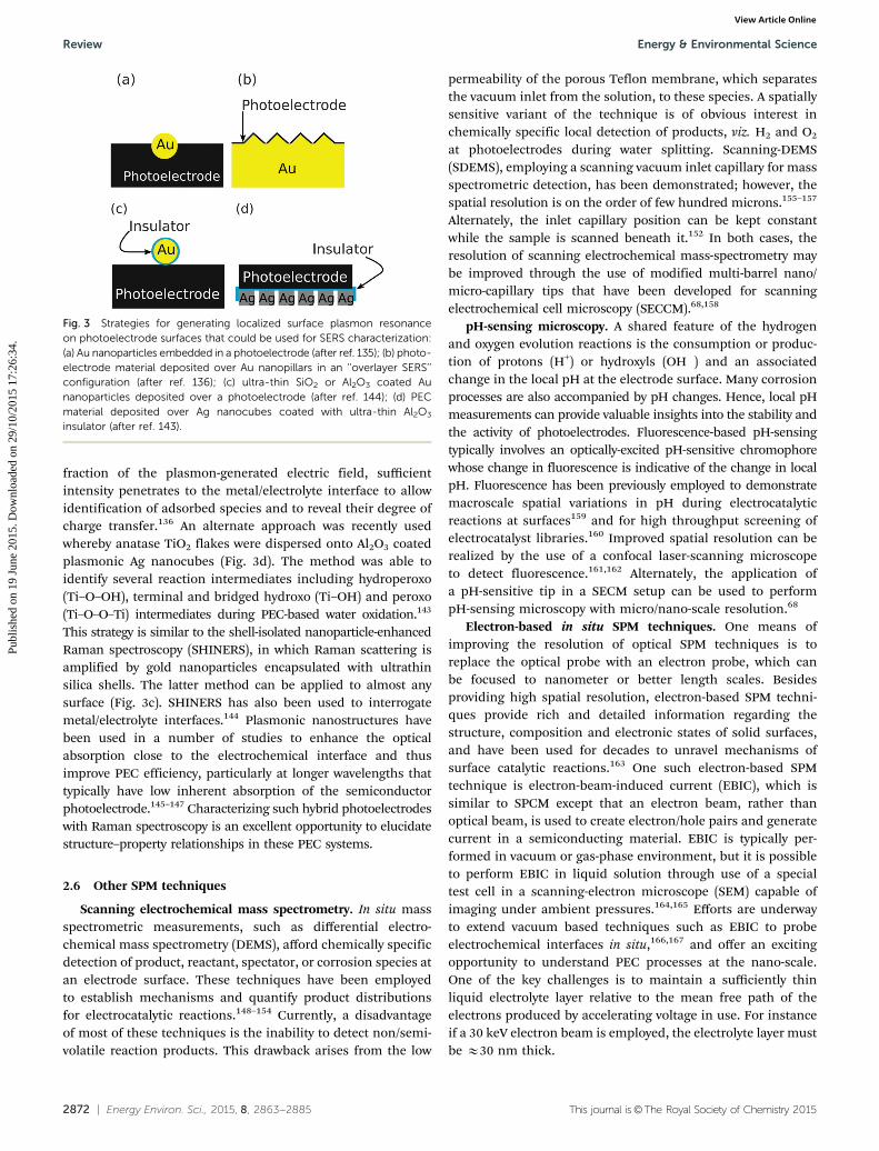
A principal weakness of Raman spectroscopy is the relativelylow scattering cross section for inelastic compared to elastic(Rayleigh) scattering, the latter being B103–106 times strongerthan the former. For most materials, the small cross section forRaman scattering necessitates the use of long sampling timesand/or high laser power to obtain acceptable signal-to-noiseratios. However, the Raman signal can be significantly enhancedby coupling the incident and/or scattered light to localizedsurface plasmons. Localized surface plasmon resonance (LSPR)is a well-recognized phenomenon in noble metal nanoparticlesand nanostructured surfaces due to collective oscillation of con-duction electrons under optical excitation, and has been exploitedfor a variety of applications, including (electro)catalysis.135–139
When optically excited, the surface plasmons re-emit theirenergy radiatively (i.e. scattering) at their resonant wavelengthor non-radiatively (i.e. absorption) by creating electron–hole pairs.Electromagnetic fields strongly enhanced at nano-protrusions ornano-gaps of a plasmonic material through a localized ‘‘antenna’’effect cause strongly amplified scattering by adsorbed molecules.The resonant wavelength not only depends on the free electrondensity and the dielectric constant of the material, but also onthe size, geometry, and dielectric constant of the surroundingmedium. Because researchers often have control of these para-meters, surfaces may be ‘tuned’ to match the excitation source.8
In surface-enhanced Raman spectroscopy (SERS), the Ramansignal of surface-adsorbed molecules is enhanced by as muchas 1014, enabling single molecule detection.140 The molecularspecificity and the rich vibronic information afforded by SERShas enabled numerous recent studies of reaction mechanismsat solid/gas and solid/liquid interfaces.109 Coupled with theintrinsic merits of Raman spectroscopy, SERS allows adsorbatevibrational spectra to be obtained over wider frequency rangesthan either IRAS or SFG, and is also characterized by morerelaxed surface-selection rules, thus allowing detection of mostvibrational modes irrespective of the molecular orientation.
A limitation of SERS is that the substrate morphology andcomposition play key roles in producing the SERS effect.Researchers often utilize samples with roughened, nano-structuredsurfaces, which can be prepared by several means includingchemical and electrochemical etching, deposition on pre-patternedsubstrates, and noble metal coating of polystyrene nanospheresdispersed on glass slides (Fig. 3a and b).141,142 Because themajority of electrocatalytically relevant metals such as Pt, Rh orNi do not efficiently sustain surface plasmons, they are coatedas ultrathin layers onto plasmonically active Au or Ag nano-structures. Although the catalyst metal overlayer attenuates a
Energy & Environmental Science Review
Publ
ishe
d on
19
June
201
5. D
ownl
oade
d on
29/
10/2
015
17:2
6:34
. View Article Online
2872 | Energy Environ. Sci., 2015, 8, 2863--2885 This journal is©The Royal Society of Chemistry 2015
fraction of the plasmon-generated electric field, sufficientintensity penetrates to the metal/electrolyte interface to allowidentification of adsorbed species and to reveal their degree ofcharge transfer.136 An alternate approach was recently usedwhereby anatase TiO2 flakes were dispersed onto Al2O3 coatedplasmonic Ag nanocubes (Fig. 3d). The method was able toidentify several reaction intermediates including hydroperoxo(Ti–O–OH), terminal and bridged hydroxo (Ti–OH) and peroxo(Ti–O–O–Ti) intermediates during PEC-based water oxidation.143
This strategy is similar to the shell-isolated nanoparticle-enhancedRaman spectroscopy (SHINERS), in which Raman scattering isamplified by gold nanoparticles encapsulated with ultrathinsilica shells. The latter method can be applied to almost anysurface (Fig. 3c). SHINERS has also been used to interrogatemetal/electrolyte interfaces.144 Plasmonic nanostructures havebeen used in a number of studies to enhance the opticalabsorption close to the electrochemical interface and thusimprove PEC efficiency, particularly at longer wavelengths thattypically have low inherent absorption of the semiconductorphotoelectrode.145–147 Characterizing such hybrid photoelectrodeswith Raman spectroscopy is an excellent opportunity to elucidatestructure–property relationships in these PEC systems.
2.6 Other SPM techniques
Scanning electrochemical mass spectrometry. In situ massspectrometric measurements, such as differential electro-chemical mass spectrometry (DEMS), afford chemically specificdetection of product, reactant, spectator, or corrosion species atan electrode surface. These techniques have been employedto establish mechanisms and quantify product distributionsfor electrocatalytic reactions.148–154 Currently, a disadvantageof most of these techniques is the inability to detect non/semi-volatile reaction products. This drawback arises from the low
permeability of the porous Teflon membrane, which separatesthe vacuum inlet from the solution, to these species. A spatiallysensitive variant of the technique is of obvious interest inchemically specific local detection of products, viz. H2 and O2
at photoelectrodes during water splitting. Scanning-DEMS(SDEMS), employing a scanning vacuum inlet capillary for massspectrometric detection, has been demonstrated; however, thespatial resolution is on the order of few hundred microns.155–157
Alternately, the inlet capillary position can be kept constantwhile the sample is scanned beneath it.152 In both cases, theresolution of scanning electrochemical mass-spectrometry maybe improved through the use of modified multi-barrel nano/micro-capillary tips that have been developed for scanningelectrochemical cell microscopy (SECCM).68,158
pH-sensing microscopy. A shared feature of the hydrogenand oxygen evolution reactions is the consumption or produc-tion of protons (H+) or hydroxyls (OH�) and an associatedchange in the local pH at the electrode surface. Many corrosionprocesses are also accompanied by pH changes. Hence, local pHmeasurements can provide valuable insights into the stability andthe activity of photoelectrodes. Fluorescence-based pH-sensingtypically involves an optically-excited pH-sensitive chromophorewhose change in fluorescence is indicative of the change in localpH. Fluorescence has been previously employed to demonstratemacroscale spatial variations in pH during electrocatalyticreactions at surfaces159 and for high throughput screening ofelectrocatalyst libraries.160 Improved spatial resolution can berealized by the use of a confocal laser-scanning microscopeto detect fluorescence.161,162 Alternately, the application ofa pH-sensitive tip in a SECM setup can be used to performpH-sensing microscopy with micro/nano-scale resolution.68
Electron-based in situ SPM techniques. One means ofimproving the resolution of optical SPM techniques is toreplace the optical probe with an electron probe, which canbe focused to nanometer or better length scales. Besidesproviding high spatial resolution, electron-based SPM techni-ques provide rich and detailed information regarding thestructure, composition and electronic states of solid surfaces,and have been used for decades to unravel mechanisms ofsurface catalytic reactions.163 One such electron-based SPMtechnique is electron-beam-induced current (EBIC), which issimilar to SPCM except that an electron beam, rather thanoptical beam, is used to create electron/hole pairs and generatecurrent in a semiconducting material. EBIC is typically per-formed in vacuum or gas-phase environment, but it is possibleto perform EBIC in liquid solution through use of a specialtest cell in a scanning-electron microscope (SEM) capable ofimaging under ambient pressures.164,165 Efforts are underwayto extend vacuum based techniques such as EBIC to probeelectrochemical interfaces in situ,166,167 and offer an excitingopportunity to understand PEC processes at the nano-scale.One of the key challenges is to maintain a sufficiently thinliquid electrolyte layer relative to the mean free path of theelectrons produced by accelerating voltage in use. For instanceif a 30 keV electron beam is employed, the electrolyte layer mustbe E30 nm thick.
Fig. 3 Strategies for generating localized surface plasmon resonanceon photoelectrode surfaces that could be used for SERS characterization:(a) Au nanoparticles embedded in a photoelectrode (after ref. 135); (b) photo-electrode material deposited over Au nanopillars in an ‘‘overlayer SERS’’configuration (after ref. 136); (c) ultra-thin SiO2 or Al2O3 coated Aunanoparticles deposited over a photoelectrode (after ref. 144); (d) PECmaterial deposited over Ag nanocubes coated with ultra-thin Al2O3
insulator (after ref. 143).
Review Energy & Environmental Science
Publ
ishe
d on
19
June
201
5. D
ownl
oade
d on
29/
10/2
015
17:2
6:34
. View Article Online

This journal is©The Royal Society of Chemistry 2015 Energy Environ. Sci., 2015, 8, 2863--2885 | 2873
3. In situ techniques for evaluation ofphotoelectrodes with high temporalresolution
Many electronic processes in photoelectrodes, such as photo-excitation, cooling, trapping, recombination, and interfacialtransfer of charge carriers, occur on sub-nanosecond timescales, and thus proceed too rapidly to be resolved by electricalmeasurements.19 Ultrafast spectroscopic techniques can probeoptical, electronic, or vibrational signatures on the requisitefemtosecond to nanosecond time scale to directly interrogatethese physical phenomena. Fig. 4a illustrates the basic conceptof a pump–probe measurement, whereby a photoexcitationpump pulse is followed after a controlled time delay by a probepulse. Fig. 4b and c provides an overview of the differentphotophysical events in an example TiO2–Pt system, alongwith an approximation of the relevant time scales for eachevent. For other materials systems, time scales for recombina-tion and reactions can also be in the sub-nanosecond range.Bench-scale pump–probe methods generally use Ti:sapphirelasers as the light source, with pulse durations that are commonlyo50 fs. These pulses can be manipulated using non-linearoptics to probe either absorption or emission over a spectralregion ranging from the ultraviolet to the far-infrared (terahertzfrequencies). The diversity of methods enables measurement ofcarrier lifetimes, transient photoconductivity, and charge trans-fer kinetics, among other phenomena. This section primarilyfocuses on transient absorption spectroscopy (TA), the mostwidely employed ultrafast method to date. An extensive reviewof ultrafast carrier dynamics for solar fuels formation has beenrecently published.19 Although this article has focused onphotoelectrode based PEC systems, TA measurements can also
be very useful for studying PEC systems based on suspensionsof photocatalytic particles, which is the topic of the reviewarticle by Ardo et al.168
TA probes the change in absorption upon photoexcitation asa function of the pump–probe delay time. Probing band-to-band transitions in the visible region reveals the electron andhole populations, while probing a sample in the IR regionprovides insight into molecular vibrations and/or conductivefree carriers. Standard TA configurations focus the opticalprobe to E300 micron spot size, although optical microscopeconfigurations such as those commonly employed in SPCMmeasurements can reduce the analysis area to length scalesclose to the optical diffraction limit. For example, TA measure-ments have been performed using a scanning focused laserbeam to perform transient absorption microscopy (TAM) forimaging micron-sized features on graphene oxide.34 The timeresolution is limited by the duration of the laser pulse, oftenE50 fs. The maximum time delay depends on the length ofthe optical delay line, and is typically several nanoseconds.Alternatively, electrical detection using a pulsed pump anda continuous probe allows measurement above nanosecondtime scales, with the maximum time determined by the laserrepetition rate. Ultrafast measurements require many lasershots to sample the desired time window with sufficient signal-to-noise ratio. Data collection often requires tens of minutes, andsamples must be stable for many turnovers under high photonfluxes. Samples should also return to their ground state beforethe next laser pulse arrives. As with SPCM techniques, the highphoton fluxes commonly employed in ultrafast spectroscopiespose a challenge when extrapolating conclusions drawn fromultrafast spectroscopy to systems operating under standard1 sun conditions. Pulse durations are short and sparse in time
Fig. 4 (a) Schematic of a generic ultrafast pump–probe spectroscopy experiment. (b) Photophysical processes and (c) their approximate time scales fordifferent steps in PEC water splitting for an example system comprising TiO2 nanoparticles decorated with Pt and IrO2 catalytic nanoparticles. Stepsinclude instantaneous photo excitation, (1) carrier cooling and trapping, (2) interphase electron transfer from TiO2 to Pt, (3) geminate recombination,(4) hydrogen evolution reaction on Pt catalyst, (5) O2 evolution on TiO2, (6) O2 evolution on Pt or IrO2, and (7) prospective O2 evolution for next-generation OER catalysts.
Energy & Environmental Science Review
Publ
ishe
d on
19
June
201
5. D
ownl
oade
d on
29/
10/2
015
17:2
6:34
. View Article Online

2874 | Energy Environ. Sci., 2015, 8, 2863--2885 This journal is©The Royal Society of Chemistry 2015
(B100 fs pulse repeated every millisecond), but the instanta-neous power is very high, often resulting in initial photoexcitedcarrier densities that are 10–1000 times larger than understeady state 1 sun conditions, and which can place the systemin the high injection regime.
Most of the early ultrafast spectroscopy studies of electronicmaterials were performed in air, but recently in situ TA hasprovided additional insight into charge-carrier dynamics. In situmeasurements present new opportunities to probe the photo-electrode–electrolyte interface under applied bias. Additionally,ultrafast spectrometers using optical delay lines to access thefs–ns time window can be stitched together with data fromspectrometers using digital delays with a ns–ms window, andwith oscilloscope-based detection and continuous probes withms–s window to provide gap-free TA spectroscopy over time-scales from femtoseconds to seconds. In a recent study ofhematite (a-Fe2O3), the current–voltage (I–V) characterizationunder pulsed laser illumination showed the expected improve-ment in absorbed-photon-to-electron collection efficiency(APCE) under positive applied potentials, but the magnitudeof the APCE was significantly lower than under 1 sun condi-tions because of excessive electron–hole recombination duringthe initial period of high photoexcited carrier densities.169
Additionally, in situ spectroelectrochemistry was used to assignspectral features to electrons and holes in the visible regionand free carriers in the mid-IR, then TA was used to probe thetime evolution of these features over fs–ms time windows.169
A feature at 570 nm was assigned to holes, and decayed at a ratethat was independent of applied bias, which indicated that thecatalytic activity of the electrodes was determined by holes withlifetimes longer than microseconds. This conclusion agrees withthat obtained by in situ microsecond TA spectroscopy, whichrevealed the presence of holes with lifetimes as long as seconds.170
The lifetime of photogenerated holes increased with appliedbias; and a linear relationship between TA amplitude at 200 msand photocurrent indicated the importance of long-lived holesin the photo-oxidation of water by Fe2O3.
Several other ultrafast techniques in addition to TA spectro-scopy are of potential interest for investigating PEC materials.Time-resolved terahertz spectroscopy (TRTS) and time-resolvedmicrowave conductivity (TRMC) have been used to measuretransient photoconductivity in semiconductors and oxides,171,172
including such relevant materials as Cu2O and BiVO4.173,174
In both of these methods, the conductivity is probed usingfar-infrared radiation. TRTS provides information on ultrafast(ps–ns) time scales, while TRMC probes the dynamics on ns–mstime scales. Both types of probes are strongly absorbed by waterand conductive electrolytes, so in situ experiments are challen-ging. However, special cell designs utilizing a back-illuminationconfiguration or very thin electrolyte layers in a recirculatingscheme to avoid build-up of photoproducts may be effective.Other ultrafast techniques of interest include time-resolved XPSand time-resolved XRD to study the surface and bulk structuralchanges that result from photoexcitation of the material or anadsorbed sensitizer.175,176 These methods require a synchro-tron source, and in situ measurements are likely to be extremely
challenging due to the nature of signal detection. Most of thetechniques outlined in this paragraph have not been appliedextensively for investigations of PEC materials and processes todate, but many opportunities exist to develop new insightsthrough the use of such methods.
4. Modeling and simulation ofphotoelectrode operation at smalllength and ultrafast time scales
Computational modeling, particularly when informed and vali-dated by the experimental techniques described in the previoussections, can be employed to offer additional insights into thekey processes that underlie operation of PEC photoelectrodes,and ultimately use that knowledge to predict new, high perfor-mance PEC materials. Unlike the experimental techniquesdiscussed up to this point, there exist many well-establishedand readily available computational modeling tools for simu-lating PEC possesses at sub-nm length scales and fs/ps timescales. While high spatial and temporal resolution are easilyobtained with computational tools, the key challenge becomesthat of ‘‘realistic’’ modeling of photoelectrodes under condi-tions that most closely approximate actual device operation.177
In this regard, computational modeling can operate hand-in-hand with in situ experimental characterization techniques,with the latter providing the needed insights into electrodestructure, chemistry, and dynamics during operation. Givenrecent advancements in both high-performance computing andcomputational algorithms, opportunities for using modelingand simulation as predictive tools for PEC studies are expand-ing.17,18,178–181 Accordingly, it is becoming increasingly evidentthat modeling and characterization efforts require tighter inte-gration as PEC research activities move forward.
Fig. 5 illustrates schematically three stages of PEC operationthat must be considered for accurate computational modelingof the entire reaction: the initial reaction setup (e.g., surface/interface formation), illumination, and final product formation.Note that the latter two stages generally overlap with the stepsin Fig. 4, encompassing photoabsorption, carrier generationand re-equilibration, charge transfer, and chemical reactivity.The first stage involves understanding how a material respondsto exposure to the environment.
The key challenge in accurately modeling the entire PEC processis that the individual contributing processes in Fig. 5 operate atintrinsically different length and time scales that cannot betreated using a single theoretical method. For instance, carriergeneration and mobility usually occur in the fs regime, whereasthe catalytic charge-transfer reaction is typically much slowerand the recombination/release/photocorrosion steps can bemuch slower still. Moreover, the results of each stage dependon those of the previous stage: the reaction chemistry and kineticpathway depends on the instantaneous interfacial structureof the photoexcited electrode surface, which in turn dependson the chemistry of the electrode surface upon electrolyteimmersion. This interdependency makes it difficult to predict
Review Energy & Environmental Science
Publ
ishe
d on
19
June
201
5. D
ownl
oade
d on
29/
10/2
015
17:2
6:34
. View Article Online

This journal is©The Royal Society of Chemistry 2015 Energy Environ. Sci., 2015, 8, 2863--2885 | 2875
with any certainty what the outcome will be, since uncertaintiesin each stage are propagated throughout the reaction. Thesolution to these difficulties is twofold. First, computationalmethods that provide different tradeoffs between accuracy andcomputational expense and that operate at different scales mustbe combined. Second, the simulations must rely on accurateexperimental probes of processes and local structures to provideinput and validation to the models and minimize error propaga-tion, particularly during the later stages of the reaction.
Broadly speaking, computational methods can be separatedinto continuum and atomistic approaches. In general, continuumapproaches provide superior flexibility for studying device opera-tion, and are capable of accessing much broader ranges of lengthand time scales. They are also well suited for examining operationunder non-equilibrium conditions and examining the overallkinetics of interdependent reaction stages, which facilitates moredirect comparison with experimentally accessible quantities. How-ever, continuum approaches provide little or no informationabout the atomic-level details of interface structure or chemistry,relying instead on parameterization by atomistic or experimentalapproaches. On the other hand, atomistic approaches are bettersuited for understanding mechanisms and chemical interactions,since they treat atoms and molecules explicitly. The disadvantageis that they are limited in the scales of systems that can beaccessed, and generally neglect broader features such as micro-structure, surface/interface inhomogeneity, interfacial bandbending, and variations in electrolyte composition.
In this section, we describe the use of atomistic computa-tional methods to accurately model physiochemical processesin operating PEC systems and better understand the mecha-nistic details that underlie PEC operation at small length and
ultrafast time scales. We do not discuss continuum-basedapproaches that could be adapted for kinetic modeling ofPEC operation; towards this end, there are a number of recentpublications and reviews describing the specific applicationof continuum models to the properties and performance ofphotoelectrodes.182–188 Nevertheless, it should be emphasizedthat one of the most pressing current research needs in the PECcommunity is the development of simulation frameworks thatcombine the power and accuracy of atomistic approaches withthe flexibility of continuum approaches. This would allow forsimulation of the kinetics of PEC operation at the system levelunder ‘‘realistic’’ conditions of varying pH, illumination, bias, andelectrolyte composition/concentration. As such unified simula-tion frameworks become available, the atomistic techniqueswe describe may be combined with continuum approaches tofurther bridge the gap between theory and experiment.
4.1 DFT and ground-state techniques
Density functional theory (DFT) in its various flavors has emerged asthe primary workhorse of first-principles computational materialsscience.189 Providing arguably the most favorable tradeoff betweencomputational cost and accuracy, DFT has been applied widelyto study the chemistry and electronic structure of photoelec-trode materials and their surfaces.181,190 It has also been usedextensively to study surface catalytic reactions, particularlyin the context of descriptor-based optimization and high-throughput screening of candidate water oxidation and protonreduction electrocatalysts.191–195 Moreover, there are several methodsavailable that can use DFT-derived energetics to directly computereaction barriers and extract free energy surfaces. These include thenudged elastic band (NEB)196 and metadynamics approaches,197
Fig. 5 Schematic of various processes and stages contributing to the complete PEC water splitting reaction (green arrow), along with possiblecomputational methods for treating the associated physical or chemical phenomena at different length and time scales. The vertical position on thegraph corresponds to the relative length scale of the process, whereas the position of the wedge where it intersects with the green arrow indicates itsrelative time scale.
Energy & Environmental Science Review
Publ
ishe
d on
19
June
201
5. D
ownl
oade
d on
29/
10/2
015
17:2
6:34
. View Article Online

2876 | Energy Environ. Sci., 2015, 8, 2863--2885 This journal is©The Royal Society of Chemistry 2015
which have found extensive usage in investigating water redoxand dissociation reactions on photocatalyst and photoelectrodematerials.198–205
An additional advantage of ground-state techniques such asDFT and ab initio molecular dynamics (AIMD) is that thesetechniques are also available for simulating spectroscopicquantities that can be compared directly with experimentalprobes, particularly at PEC interfaces. These include computationof IR/Raman spectra,206–208 as well as XAS/XES209–212 spectra.Methods that require explicit treatment of excited states, suchas UV-vis/IR optical spectroscopy, are covered in the nextsection. These experimental techniques offer a viable pathwayfor model validation.
Historically, much of the DFT-based work has focused onstudying bulk electrodes and their idealized surfaces invacuum. Recently, there has been growing interest in extendingthe application of DFT to study interfaces between electrodesand electrolytes, which require large simulation cells that cantreat both components on equal footing. This trend can beconsidered analogous to the adoption of in situ techniques inexperimental characterization. Typically, consideration of theliquid electrolyte also requires explicit treatment of atomisticdynamics in an ab initio molecular dynamics scheme (AIMD;alternatively, first-principles MD or DFT-MD), which relies on DFT-computed forces to propagate atomic trajectories. Examininginterfaces using DFT is further complicated by a general lack ofunderstanding of how surfaces and surface reconstructionsform in solution as compared to their vacuum counterparts.Nevertheless, several groups have adopted AIMD approaches tostudy the structure and chemistry of semiconductor–waterinterfaces for PEC applications.198,201,213–225 The presence ofsemiconductor surfaces often significantly alters the dynamicaland chemical properties of water; conversely, the presence of theelectrolyte can significantly alter the physiochemical properties ofthe semiconductor. Accordingly, recent simulations have reporteda wide variety of complex chemical processes active at semi-conductor surfaces when liquid water is included explicitly,such as water dissociative adsorption,198,201,214,216–218,221,222,224
surface hydroxylation and radical formation,198,201,214,216–219,221,223
unusual changes in the hydrogen-bond network,198,201,213–220
and fast surface proton hopping.198,214–217 It is also possible toassess surface acidity/basicity based on AIMD simulations ofwater-semiconductor interfaces when water dissociation isactive.214,217,226 Collectively, these reports point to the impor-tance of the specific interaction between the electrode and theelectrolyte in determining the physiochemical properties ofthe interface and the associated reaction mechanisms, andhighlight the future need for consideration of both species inaccurate models of PEC operation.
An alternative to explicit inclusion of the full electrolyte inAIMD simulations is to describe some portion of the electrolyteusing an implicit solvation scheme that combines traditionalDFT with polarizable continuum models. This approach has longbeen used in the quantum chemistry community to study ionicand molecular solvation,227 and similar ideas are now beginningto be adapted for solid–liquid interfaces.228–232 Such polarizable
continuum-based schemes can also mitigate another criticalchallenge for realistic simulations of electrode–electrolyte inter-faces and catalytic redox electrochemistry—namely, the applica-tion of a well-defined voltage bias or photo-bias. Typically, thereare two complications associated with an external bias within DFT:first, charge neutrality considerations that prevent accurate deter-mination of a potential reference for a charged system that can bedirectly compared with experiments; and second, fundamentalincompatibilities with the periodic boundary conditions generallyemployed for simulations of extended crystalline systems. Specificapproaches for dealing with these shortcomings have been outlinedwithin the context of the effective screening medium (ESM),231,232
joint DFT (JDFT)233–235 and self-consistent continuum solvation(SCCS)230,236 methodologies. Alternative schemes for defininguniversal potential references for PEC-relevant reactions inDFT/AIMD have also been proposed.237–239
Implementations of the abovementioned techniques are rathernew, and in most cases their application has been confined tometallic electrodes. Nevertheless, they present a promisingapproach for considering [photo]voltage-dependent electronic,dynamical, and structural effects observed at semiconductor–liquid PEC interfaces during operation. One example is thecomplex relationship between the structure and dynamics ofthe electric double layer and the space-charge effect it induces onthe charged photoelectrode. They also open up the possibility ofdirectly examining the mechanisms and kinetics of charge-transferreactions at PEC interfaces under bias. In this latter case, one mustbe careful to consider the distinction between the more commonlyemployed constant-charge scheme and the more experimentallyrelevant constant-potential scheme.240 The recently proposedpotentiostat method of Bonnet and Otani232 is an example of aconstant-potential scheme that could be implemented directlywithin AIMD to permit dynamics at a fixed bias that betterrepresents experimental conditions in a PEC cell.
Despite their predictive power, conventional DFT and AIMDhave some significant theoretical limitations that are relevantfor investigations of PEC materials. One of these is an inabilityto correctly describe charge localization, particularly in stronglycorrelated electronic systems. This shortcoming can proveparticularly problematic for simulating charge transport withinmany transition-metal oxides, where conductivity may be drivenby a polaronic hopping mechanism rather than direct bandtransport (e.g., alpha-Fe2O3).190,241–243 In such systems, chargetransport is often the rate-limiting process, making accuratetheoretical description paramount. To a large extent, this limita-tion can be overcome by adoption of more advanced exchange–correlation functionals that include some amount of exactHartree–Fock exchange (so-called hybrid functionals)223,244 orHubbard corrections (DFT+U).245 The appropriate amount ofexact exchange or +U to include is generally system dependent,and can be determined empirically or else directly from ab initiocalculations.246–249 In the case of hybrid functionals, the addi-tional computational expense can also significantly limit AIMDsimulation times, particularly when applied to solid–liquidinterfaces. Second, DFT is inherently a ground-state method,and thus cannot in general provide an accurate description of
Review Energy & Environmental Science
Publ
ishe
d on
19
June
201
5. D
ownl
oade
d on
29/
10/2
015
17:2
6:34
. View Article Online

This journal is©The Royal Society of Chemistry 2015 Energy Environ. Sci., 2015, 8, 2863--2885 | 2877
excited-state properties. For instance, it is well-known that DFTunderestimates band gap and cannot quantitatively predictvalence and conduction band edge positions.237,250 It also preventstreatment of electronic excited-state dynamics and true photo-illumination conditions.177 Accordingly, it is better suited toexamining interfaces in the dark, although the next sectionprovides a brief overview of excited-state and beyond-DFTmethods that can be incorporated to address this limitation.
Occasionally, it may become necessary to determine quantitiessuch as adsorbate binding energies and dissociation barriers witheven higher accuracy than DFT can generally provide (for instance,to be used as inputs in coarse-grained or model-Hamiltonianapproaches). In these cases, more advanced methods maybe invoked at the cost of additional computational expense.These include higher-order perturbative quantum chemicalmethods,251,252 as well as quantum Monte Carlo (QMC),253 whichsolves the electronic wavefunction stochastically. These methodsare currently limited in the system sizes they can access and aredifficult to implement in a dynamics framework, and havetherefore not been widely applied to PEC materials. However,a more realistic use may be for benchmarking DFT calculationson model systems and informing the proper choice of DFTexchange–correlation functionals, or else for systematic refine-ment of energetics.
4.2 Excited-state and beyond-DFT methods
Proper simulation of the optical excitations associated withphotoelectrode illumination or with optical probe techniquesrequires augmenting ground-state DFT with higher-order methodsthat consider electronic excited states. An overview of thesemethods is included in this section, and a more detaileddiscussion can be found in a recent review by Ping et al.177
In general, excited-state methods carry significantly highercomputational expense than ordinary ground-state DFT, andare therefore limited to much smaller systems and time scales.One of the most popular excited-state methods is the extensionof the ground-state DFT formalism known as time-dependentDFT (TDDFT),254–256 which relies on full solution of the time-dependent Schrodinger equation within a set of prescribedapproximations. TDDFT allows one to simulate oscillator strengthsand vertical excitations for all relevant electronic transitions. It cantherefore be used to describe the optical absorption spectrum of amodel photoelectrode, or to understand how bulk absorptionstates change at surfaces or interfaces. In addition, TDDFT-basedapproaches can provide excited-state electron dynamics in the fsregime, which is a useful tool for directly simulating ultrafastpump–probe experiments. Such techniques may enable investiga-tions of charge carrier dynamics that are directly relevant to PECdevices, including interfacial charge transfer between co-catalystsand photoabsorbers, or through semiconductor–insulator–metal junctions. To date, probably the most mature applicationof TDDFT to photoelectrode materials has been in the contextof carrier injection and transport in dye-sensitized TiO2.257–259
For certain semiconductors, TDDFT may be inadequatefor accurately predicting photoexcitation spectra.177,256 In theseinstances, more accurate determination of electronic excitations
can be achieved using methods based on many-body perturba-tion theory and the Green’s function formalism.260 The GWapproximation is the current state-of-the-art for the calcula-tions of quantities obtained from photoemission spectroscopymeasurements (PES, XPS), such as semiconductor band gapsand band edge alignments.261 Similarly, the Bethe–Salpeter(BSE) equation, which employs two-particle Green’s functions,provides a reliable approach for describing optical absorptionprocesses that involve electron–hole interactions.262 Histori-cally, these techniques have been considered too expensivefor application to PEC interfaces; however, recent algorithmicdevelopments263–265 allows one to apply the GW method tolarger system sizes, permitting direct treatment of both the solidelectrode and liquid electrolyte.266–270 This opens up opportu-nities to investigate how local electronic states are altered by thepresence of the liquid electrolyte within a formalism that is oftenmore robust than TDDFT, and provides a possible templatefor comparison with high-resolution experimental probes. Asalternatives to the GW/BSE approach, high-level quantumchemistry methods such as Møller–Plesset perturbation theory(MPn),271 coupled cluster theory (CC),272 configuration interaction(CI),273 complete active space self-consistent field (CASSCF),274
and complete active space with second-order perturbation theory(CASPT2)275 can be employed to calculate excited-state properties.To date, these approaches have been applied primarily tomolecules and nanostructures.276,277 Developments to extendthese approaches to study solids are underway; however,further advances are required before they can be used to studyPEC interfaces.278,279
Although TDDFT, GW, and BSE techniques can be used todetermine the electronic structure of a photoelectrode materialupon optical excitation, they do not provide the excited-statedynamics of atoms and ions. To this end, a promising emergingdirection involves coupling excited-state electronic dynamics(in particular, TDDFT) with AIMD to investigate the effect ofphotoexcitation on the nonadiabatic dynamical evolution of thesurface atoms and adsorbates.259,280–282 One such implementa-tion was recently applied by the Prezhdo group to study non-adiabatic processes in photoinduced water splitting on GaN,283
and has found similar successes in studies of photocatalyticprocesses on metal oxides.259 Naturally, the simulation timesthat can be achieved are limited by the time scale of the electrondynamics (fs regime), but ultrafast responses can be studied.At present, it is unclear under which conditions such non-adiabatic atomic responses can be relevant to the reactionmechanisms on PEC photoelectrodes, but it represents anexciting future research pathway.259
4.3 Coarse-grained, model-Hamiltonian, and force-fieldapproaches
Among the most significant limitations of DFT-based techniquesis an inability to access the larger length (beyond a few nm) andtime scales (beyond hundreds of ps) required to investigate laterreaction stages or to fully describe variations in the electrodemicrostructure or electrolyte composition. As discussed above,a possible solution is to combine atomistic approaches with
Energy & Environmental Science Review
Publ
ishe
d on
19
June
201
5. D
ownl
oade
d on
29/
10/2
015
17:2
6:34
. View Article Online

2878 | Energy Environ. Sci., 2015, 8, 2863--2885 This journal is©The Royal Society of Chemistry 2015
continuum approaches. However, in the absence of a unifiedframework, atomistic approaches that take advantage of coarsegraining, simplified model Hamiltonians, and parameterizedclassical potentials can also push closer to accessing morerealistic system sizes and much longer simulation times.
Classical molecular dynamics approaches based on inter-atomic potentials that are fit to experimental or ab initio-derivedproperties represent one option for scaling to 4mm system sizesand 4ns simulation times. These techniques make it possible toaccount for the full composition and evolution of the liquidelectrolyte (even at low ion concentrations or weakly acidic/alkaline conditions, which typically require very large simula-tions), as well as many features in the electrode microstructure.However, a key difficulty lies in the proper parameterization ofthe interatomic potentials, which must be valid not only fordescribing bulk properties of the electrode and electrolyte, butalso the interface between the two. By contrast, AIMD is based onfirst-principles descriptions that are agnostic to the chemicalenvironment. A second obstacle that is particularly relevantto PEC hydrogen or oxygen evolution is the inability of mostclassical dynamics frameworks to properly treat chemical reactionsthat involve bond breaking and forming. Currently, the mostattractive solution to these difficulties is to use methods basedon reactive classical potentials/force fields that are specificallydesigned to permit bond breaking/forming and are ‘‘trained’’using data from smaller AIMD runs. In recent years, the ReaxFFtechnique284 has emerged as the best known reactive force-fieldmethod, and has been successfully applied to the study of a fewsemiconductor–liquid interfaces.285–287 However, additionalwork on training ReaxFF potentials using AIMD needs to bedone in order to improve the transferability and predictivepower of such techniques for other photoelectrode materials,particularly given the sensitivity of the potential parameters tothe particular surface and electrolyte composition.
Alternatively, one can abandon real-time dynamics in favorof stochastic approaches that offer insight into PEC reactionkinetics and transport processes based on model Hamiltonians.One of the most powerful model-Hamiltonian techniques is kineticMonte Carlo (kMC), which can take advantage of ab initio-derivedreaction and diffusion barriers (e.g., from DFT or QMC) to predictoverall reaction kinetics. Techniques based on kMC are attractivebecause they are extraordinarily flexible and capable of accessingwide ranges of timescales depending on the specific level ofspatiotemporal discretization. However, they generally rely ondecomposing PEC reactions into well-defined reaction steps,each with a well-defined barrier. Given the inherent complexityand inhomogeneity of semiconductor–electrolyte interfaces, thiscan be extremely difficult in practice. Nevertheless, when usedappropriately, kMC is well suited to offer semi-quantitativedescriptions of reaction kinetics and charge transport processesthat can be directly compared with experimental probes. Forinstance, kMC techniques have been used to study chargetransport in hematite288 and through grain boundaries in poly-crystalline TiO2.289 The latter example illustrates how kMC canbe applied to amorphous systems based on an averaged homo-geneous description, which presents extraordinary challenges
for conventional DFT-based models that rely on actual atomicconfigurations. Model-Hamiltonian techniques have also beenadopted to refine PEC reaction barriers in the presence ofthe liquid electrolyte. An excellent example is the approachintroduced by Santos et al.,290 which uses an Anderson–Newnsmodel in conjunction with ordinary DFT to predict protonabstraction barriers. This same method was recently success-fully applied to the catalytic hydrogen evolution on the PECelectrode material MoS2.291
Another issue that can plague DFT studies of photoelectrodesurfaces is the complexity in surface structure and atomicarrangement, particularly for alloys, defect- or adsorbate-richsurfaces, and amorphous or polycrystalline electrodes. Similarchallenges exist for examining atomic structures at the solidinterface between the semiconductor and the catalyst. There iscurrently no definitive solution to these difficulties, emphasizingthe need for high-fidelity experimental characterization to informatomistic models. Nevertheless, approaches have typically reliedon decomposing the material into local building blocks that canbe computed explicitly, which are then combined to generate andpredict new low-energy structures. This can be done by qualita-tive observations of local chemical similarities in simplifiedmodels,292 or else by using rigorously defined mathematicalmethodologies. In the latter category, one of the most popularapproaches is the cluster expansion method,293 which has beenapplied successfully to efficiently determine bulk and surfacealloy compositions of crystalline photoelectrode materials.294–298
The cluster expansion method relies on mapping the composi-tional variation onto an Ising-like lattice-gas model Hamiltonian,each ‘‘site’’ of which may be independently occupied (or unoccupied)by a given substitutional species. Accordingly, its accuracy dependson the reliability of the lattice-gas mapping, which is limited towell-defined bulk or surface structures. For instance, it can beadapted to study lattice point defects, but it is not suitable foramorphous materials. The lattice-gas assumption must also berigorously verified for PEC surfaces in an electrolyte solution, whichcan be highly dynamic and facilitate large atomic rearrangements.
5. Special topics5.1 Coordinating high resolution in situ measurements withtraditional, macro-scale measurements
Although the in situ experimental techniques discussed in thisarticle can provide valuable information about photoelectrodeproperties at small length and fast time scales, the experimentalconditions for these measurements are often very different fromthose involved with real device operating conditions. For example,differences in the local and global reaction rates, in addition todifferences in the intensity, uniformity, and spectral characteris-tics of the light source, are common. Hence, results obtained fromnano- or micro-scale measurements must be extrapolated withsuitable caveats to predict or explain macroscopic photoelectrodeperformance under AM 1.5 operating conditions. When possible,nano/micro and macro measurements should be performedunder similar conditions. Unfortunately, trade-offs are often
Review Energy & Environmental Science
Publ
ishe
d on
19
June
201
5. D
ownl
oade
d on
29/
10/2
015
17:2
6:34
. View Article Online

This journal is©The Royal Society of Chemistry 2015 Energy Environ. Sci., 2015, 8, 2863--2885 | 2879
present between signal-to-noise ratio, resolution, and mimick-ing realistic PEC device operating conditions. For both nano/micro and macro-scale measurements, data can be collectedover a range of operating conditions, such as light intensity orapplied potential, to ascertain the sensitivity of the measureddifferences in behavior to operating conditions and thus gaininsight into the validity of direct quantitative comparisonbetween measurements at different length scales.
Scanning-probe measurements are necessarily local measure-ments, the output of which will naturally vary across the macro-scopic surface. The variation in a measured property across amacroscopic sample surface can be quantified by performing thehigh resolution measurement at multiple microscopic regions, asis commonly done in electron microscopy. Having performedlocal SPM measurements at multiple locations, variation in thenano or micro-scale signal can be compared with macro-scalemeasurements. Whenever possible, observations and conclusionsdrawn from micro- and nano-scale measurements should becross-checked by the use of more traditional, macro-scale PECmeasurements (e.g., using an AM 1.5 light source) and/or compu-tational modeling tools. Detailed descriptions of the standardprotocols for commonly employed macro-scale PEC measure-ments, such as current–voltage characteristics and quantum yieldmeasurements can be found in the literature.299,300
5.2 Combined in situ techniques
All of the SPM techniques in Table 1 can provide valuable informa-tion about photoelectrode materials when performed individually,but a much more complete view of photoelectrode operation canbe obtained when multiple SPM techniques are combined in thesame measurement platform and performed simultaneously.301
Such combined or multifunctional in situ measurement platformsrepresent a powerful means of obtaining complementary informa-tion that can more easily elucidate complex structure–propertyrelationships. Importantly, performing multiple measurementssimultaneously ensures that identical experimental conditions areemployed for each technique and on the same nano- or microscopicarea of the photoelectrode. In contrast, it can be difficult to achieveidentical analytical and electrode surface conditions when two ormore independent in situ measurements are conducted sequen-tially, especially if different electrochemical test cells are employedfor each technique.
Many examples of combined in situ measurements have beendemonstrated for electrochemical or photoelectrochemical systems.The combination of SECM with AFM has been used to correlatenano- or micron-scale variation in (photo)catalytic activity to topo-logical features such as grain boundaries, catalyst particles, andmore.113,301,302 Combined AFM/STM enables simultaneous mea-surements of the force and conductance curves of two impingingdouble layers in the electrochemical environment, while thenatural pairing of Raman mapping and SPCM offers the abilityto investigate variations in local photocurrent as a function ofthe chemical or physical nature of the photoelectrode surface.Other examples of combined in situ measurements that have beenreported include SPCM/SECM,12,31,56,58,303 SPCM/shear force topo-graphy,45 SECM/AFM,301 and Raman/SPCM,304 SECM/optical
microscopy(OM),305,306 ECSTM/SECM,93,94,307 NSOM/fluores-cence spectroscopy,308,309 and ECSTM/TERS.310,311 The capabilitiesof these various multifunctional set-ups are vast, and their useful-ness will vary substantially from material to material, making someset-ups better suited than others for investigating certain PECmaterials and/or chemistries.
6. Conclusions and future outlook
The continued development of experimental and computationaltechniques to study photoelectrochemical systems with highspatial and temporal resolution can provide a more completeunderstanding of fundamental PEC processes and thus aid in thedevelopment of commercially viable PEC technology. This reviewhas described several types of experimental and computationaltools that are well-suited for achieving these objectives. Particularemphasis has been placed on experimental techniques that caninvestigate photoelectrode properties in situ, providing valuableinformation about properties and performance in the photo-electrochemical environment. Scanning probe measurement tech-niques are especially useful for interrogating photoelectrodes atsmall length scales, while time resolved pump–probe spectro-scopy techniques are well-suited for studying PEC processes atvery fast time scales. Atomistic modeling tools provide the abilityto unlock mechanisms of PEC processes at the smallest lengthand fastest time scales, which in many cases are not currentlyaccessible with experimental techniques. When informed by andused in coordination with experimental techniques, computa-tional techniques may offer PEC researchers unique abilities todiscover and design photoelectrode materials through an under-standing of photoelectrode operation.
Nearly all of the techniques described in this review possessmajor challenges or limitations in their successful application toPEC systems. Many techniques have inherent limitations onlength and time scales that can be described, or are only compa-tible with certain materials and/or photoelectrode morphologies.Another key challenge in the development of in situ experimentaltechniques and computational tools for studying PEC systems atsmall length and fast time scales is their application at operatingconditions that are relevant to real-world PEC operation under AM1.5 illumination. Improvement in hardware, software algorithms,and experimental set-ups germane to current techniques willcontinue to be important for overcoming these limitations, as willthe careful coordination of multiple experimental and computa-tional techniques to bridge length and time scales. Together, theseapproaches will enable a suite of tools that should significantlyaccelerate the discovery, design, and optimization of materialsfor solar-driven water splitting with photoelectrochemical cells.
Acknowledgements
The authors thank Dr. Eric Miller for the inspiration to compilethis review, and the members of the U.S. Department of Energy’sPhotoelectrochemical Working Group and Task 35 (RenewableHydrogen) of the International Energy Agency’s Hydrogen
Energy & Environmental Science Review
Publ
ishe
d on
19
June
201
5. D
ownl
oade
d on
29/
10/2
015
17:2
6:34
. View Article Online

2880 | Energy Environ. Sci., 2015, 8, 2863--2885 This journal is©The Royal Society of Chemistry 2015
Implementing Agreement for helpful comments, suggestions,and discussions. DVE acknowledges support from the NISTNational Research Council postdoctoral Fellowship Program.JMV and NSL would like to acknowledge the Joint Center forArtificial Photosynthesis, a DOE Energy Innovation Hub, sup-ported through the Office of Science of the U.S. Department ofEnergy under Award No. DE-SC0004993 and the NationalScience Foundation Grant CHE-1214152. JMV acknowledgessupport through a NRC Ford Foundation Postdoctoral Fellow-ship. JJ thanks the Camille and Henry Dreyfus Foundation forfinancial support through its postdoctoral fellowship programin environmental chemistry. JBB acknowledges support fromNSF ECCS-1201957 and NSF CBET-1333649. BW and TOacknowledge support from the Fuel Cell Technologies Programwithin the DOE Office of Energy Efficiency and RenewableEnergy. T.A.P acknowledges support from the Lawrence Fellow-ship. A portion of this work was performed under the auspicesof the U.S. Department of Energy by Lawrence Livermore NationalLaboratory under Contract DE-AC52-07NA27344. Sandia is a multi-program laboratory operated by Sandia Corporation, a LockheedMartin Company, for the U.S. DOE National Nuclear SecurityAdministration under Contract DE-AC04-94AL85000. AAT was sup-ported by Science of Precision Multifunctional Nanostructures forElectrical Energy Storage (NEES), an Energy Frontier ResearchCenter funded by the U.S. Department of Energy, Office of Science,and Office of Basic Energy Sciences under award DESC0001160.A summary version of this review paper (DOI: 10.2172/1209497),and associated summary tables that will be updated as the fieldprogresses, will be available on the working group website (http://energy.gov/eere/fuelcells/photoelectrochemical-working-group).
References
1 M. Gratzel, Nature, 2001, 414, 338–344.2 J. Turner, G. Sverdrup, M. K. Mann, P. C. Maness,
B. Kroposki, M. Ghirardi, R. J. Evans and D. Blake, Int.J. Energy Res., 2008, 32, 379–407.
3 M. G. Walter, E. L. Warren, J. R. McKone, S. W. Boettcher, Q. Mi,E. A. Santori and N. S. Lewis, Chem. Rev., 2010, 110, 6446–6473.
4 N. S. Lewis, ECS Interface, 2013, 22, 43–50.5 US DOE Multi-Year Res. Dev. Demonstr. Plan, 2012.6 J. R. McKone, N. S. Lewis and H. B. Gray, Chem. Mater.,
2014, 26, 407–414.7 A. Fujishima and K. Honda, Nature, 1972, 238, 37–38.8 A. Kudo and Y. Miseki, Chem. Soc. Rev., 2009, 38, 253–278.9 E. L. Miller, N. Gaillard, J. Kaneshiro, A. DeAngelis and
R. Garland, Int. J. Energy Res., 2010, 34, 1215–1222.10 X. Chen, S. Shen, L. Guo and S. S. Mao, Chem. Rev., 2010,
110, 6503–6570.11 P. C. K. Vesborg and T. F. Jaramillo, RSC Adv., 2012, 2,
7933–7947.12 J. Lee, H. Ye, S. Pan and A. J. Bard, Anal. Chem., 2008, 80,
7445–7450.13 H. Ye, J. Lee, J. S. Jan and A. J. Bard, J. Phys. Chem. C, 2010,
114, 13322–13328.
14 G. Liu and A. J. Bard, J. Phys. Chem. C, 2010, 114, 17509–17513.15 J. H. He and B. A. Parkinson, ACS Comb. Sci., 2011, 13,
399–404.16 J. M. Gregoire, C. X. Xiang, X. N. Liu, M. Marcin and J. Jin,
Rev. Sci. Instrum., 2013, 84, 024102.17 J. Greeley, T. F. Jaramillo, J. Bonde, I. B. Chorkendorff and
J. K. Norskov, Nat. Mater., 2006, 5, 909–913.18 I. E. Castelli, T. Olsen, S. Datta, D. D. Landis, S. Dahl,
K. S. Thygesen and K. W. Jacobsen, Energy Environ. Sci.,2012, 5, 5814–5819.
19 J. B. Baxter, C. Richter and C. A. Schmuttenmaer, Annu.Rev. Phys. Chem., 2014, 65, 423–447.
20 N. S. Lewis, Acc. Chem. Res., 1990, 23, 176–183.21 A. J. Nozik and R. Memming, J. Phys. Chem., 1996, 100,
13061–13078.22 W. A. Smith, I. D. Sharp, N. Strandwitz and J. Bisquert,
Energy Environ. Sci., 2015, DOI: 10.1039/C5EE01822F.23 A. Minguzzi, D. Battistel, J. Rodrıguez-Lopez, A. Vertova,
S. Rondinini, A. J. Bard and S. Daniele, J. Phys. Chem. C,2015, 119, 2941–2947.
24 C. Bhattacharya, H. C. Lee and A. J. Bard, J. Phys. Chem. C,2013, 117, 9633–9640.
25 K. M. Nam, H. S. Park, H. C. Lee, B. H. Meekins, K. C.Leonard and A. J. Bard, J. Phys. Chem. Lett., 2013, 4, 2707–2710.
26 X. Zhang, H. Li, S. Wang, F. R. F. Fan and A. J. Bard, J. Phys.Chem. C, 2014, 118, 16842–16850.
27 K. C. Leonard, K. M. Nam, H. C. Lee, S. H. Kang, H. S. Parkand A. J. Bard, J. Phys. Chem. C, 2013, 117, 15901–15910.
28 S. P. Berglund, H. C. Lee, P. D. Nunez, A. J. Bard and C. B.Mullins, Phys. Chem. Chem. Phys., 2013, 15, 4554–4565.
29 B. Moralejo, M. A. Gonzalez, J. Jimenez, V. Parra, O. Martınez,J. Gutierrez and O. Charro, J. Electron. Mater., 2010, 39, 663–670.
30 W. Warta, Sol. Energy Mater. Sol. Cells, 2002, 72, 389–401.31 D. V. Esposito, I. Levin, T. P. Moffat and A. A. Talin, Nat.
Mater., 2013, 12, 562–568.32 R. Graham and D. Yu, Mod. Phys. Lett. B, 2013, 27, 1330018.33 E. Abbe, Arch. Mikrosk. Anat., 1873, 9, 413–418.34 R. Kopelman and W. Tan, Science, 1993, 262, 1382–1384.35 Q. Wu, G. D. Feke, R. D. Grober and L. P. Ghislain, Appl.
Phys. Lett., 1999, 75, 4064–4066.36 Z. Wang, W. Guo, L. Li, B. Luk’yanchuk, A. Khan, Z. Liu,
Z. Chen and M. Hong, Nat. Commun., 2011, 2, 218.37 L. Kastrup, H. Blom, C. Eggeling and S. Hell, Phys. Rev.
Lett., 2005, 94, 178104.38 V. Westphal and S. Hell, Phys. Rev. Lett., 2005, 94, 143903.39 K. Y. Han, S. K. Kim, C. Eggeling and S. W. Hell, Nano Lett.,
2010, 10, 3199–3203.40 E. Betzig and J. K. Trautman, Science, 1992, 257, 189–195.41 C. M. Harris, Anal. Chem., 2003, 75, 223A–228A.42 C. R. McNeill, H. Frohne, J. L. Holdsworth, J. E. Furst,
B. V. King and P. C. Dastoor, Nano Lett., 2004, 4, 219–223.43 M. S. Leite, M. Abashin, H. J. Lezec, A. G. Gianfrancesco,
A. A. Talin and N. B. Zhitenev, IEEE J. Photovolt., 2014, 4,311–316.
44 M. S. Leite, M. Abashin, H. J. Lezec, A. Gianfrancesco, A. A.Talin and N. B. Zhitenev, ACS Nano, 2014, 8, 11883–11890.
Review Energy & Environmental Science
Publ
ishe
d on
19
June
201
5. D
ownl
oade
d on
29/
10/2
015
17:2
6:34
. View Article Online

This journal is©The Royal Society of Chemistry 2015 Energy Environ. Sci., 2015, 8, 2863--2885 | 2881
45 L. F. Garfias-Mesias and W. H. Smyrl, J. Electrochem. Soc.,1999, 146, 2495–2501.
46 S. Kawata, Y. Inouye and P. Verma, Nat. Photonics, 2009, 3,388–394.
47 M. Burghard and A. Mews, ACS Nano, 2012, 6, 5752–5756.48 M. D. Kelzenberg, D. B. Turner-Evans, B. M. Kayes,
M. A. Filler, M. C. Putnam, N. S. Lewis and H. A. Atwater,Nano Lett., 2008, 8, 710–714.
49 A. J. Bard and M. V. Mirkin, Scanning ElectrochemicalMicroscopy, Taylor & Francis, 2nd edn, 2012.
50 M. V. Mirkin, W. Nogala, J. Velmurugan and Y. Wang,Phys. Chem. Chem. Phys., 2011, 13, 21196–21212.
51 A. J. Bard and M. V. Mirkin, Scanning ElectrochemicalMicroscopy, Taylor & Francis, 2001.
52 S. Amemiya, A. J. Bard, F. R. F. Fan, M. V. Mirkin andP. R. Unwin, Annu. Rev. Anal. Chem., 2008, 1, 95–131.
53 P. Bertoncello, Energy Environ. Sci., 2010, 3, 1620.54 H. S. Park, K. C. Leonard and A. J. Bard, J. Phys. Chem. C,
2013, 117, 12093–12102.55 D. Bae, T. Pedersen, B. Seger, M. Malizia, A. Kuznetsov,
O. Hansen, I. Chorkendorff and P. C. K. Vesborg, EnergyEnviron. Sci., 2015, 8, 650–660.
56 N. Casillas, P. James and W. H. Smyrl, J. Electrochem. Soc.,1995, 142, L16.
57 P. James, N. Casillas and W. H. Smyrl, J. Electrochem. Soc.,1996, 143, 3853.
58 W. Liu, H. Ye and A. J. Bard, J. Phys. Chem. C, 2010, 114,1201–1207.
59 J. Velmurugan, P. Sun and M. V. Mirkin, J. Phys. Chem. C,2009, 113, 459–464.
60 P. Sun and M. V. V. Mirkin, Anal. Chem., 2006, 78,6526–6534.
61 D. O. Wipf, A. J. Bard and D. E. Tallman, Anal. Chem., 1993,65, 1373–1377.
62 M. A. Edwards, A. L. Whitworth and P. R. Unwin, Anal.Chem., 2011, 83, 1977–1984.
63 K. McKelvey, M. A. Edwards and P. R. Unwin, Anal. Chem.,2010, 82, 6334–6337.
64 S. E. Pust, M. Salomo, E. Oesterschulze and G. Wittstock,Nanotechnology, 2010, 21, 105709.
65 H. Shin, P. J. Hesketh, B. Mizaikoff and C. Kranz, Anal.Chem., 2007, 79, 4769–4777.
66 J. Wiedemair, B. Balu, J. Moon, D. W. Hess, B. Mizaikoffand C. Kranz, Anal. Chem., 2008, 80, 5260–5265.
67 Y. Wang, K. Kececi, J. Velmurugan and M. V. Mirkin, Chem.Sci., 2013, 4, 3606.
68 B. P. Nadappuram, K. McKelvey, R. Al Botros, A. W. Colburnand P. R. Unwin, Anal. Chem., 2013, 85, 8070–8074.
69 A. Davoodi, J. Pan, C. Leygraf and S. Norgren, Electrochem.Solid-State Lett., 2005, 8, B21.
70 K. Eckhard, M. Etienne, A. Schulte and W. Schuhmann,Electrochem. Commun., 2007, 9, 1793–1797.
71 T. E. Lister and P. J. Pinhero, Electrochim. Acta, 2003, 48,2371–2378.
72 R. M. Souto, Y. Gonzalez-Garcıa and S. Gonzalez, Corros.Sci., 2005, 47, 3312–3323.
73 N. Casillas, S. J. Charlebois, W. H. Smyrl and H. S. White,J. Electrochem. Soc., 1993, 140, L142–L145.
74 P. I. James, L. F. Garfias-Mesias, P. J. Moyer andW. H. Smyrl, J. Electrochem. Soc., 1998, 145, L64–L66.
75 J. Rodrıguez-Lopez, M. A. Alpuche-Aviles and A. J. Bard,J. Am. Chem. Soc., 2008, 130, 16985–16995.
76 J. Rodrıguez-Lopez and A. J. Bard, J. Am. Chem. Soc., 2010,132, 5121–5129.
77 Q. Wang, J. Rodrıguez-Lopez and A. J. Bard, J. Am. Chem.Soc., 2009, 131, 17046–17047.
78 B. H. Simpson and J. Rodrıguez-Lopez, Electrochim. Acta,2015, DOI: 10.1016/j.electacta.2015.04.128.
79 B. H. Simpson and J. Rodrıguez-Lopez, Anal. Methods,2015, DOI: 10.1039/C5AY00503E.
80 M. Zhou, Y. Yu, K. Hu and M. V. Mirkin, J. Am. Chem. Soc.,2015, DOI: 10.1021/ja512482n.
81 P. R. Unwin and A. J. Bard, J. Phys. Chem., 1991, 95, 7814–7824.82 A. J. Bard, M. V. Mirkin, P. R. Unwin and D. Wipf, J. Phys.
Chem., 1992, 96, 1861–1868.83 F. Zhou, P. R. Unwin and A. J. Bard, J. Phys. Chem., 1992,
4924, 4917–4924.84 C. J. Slevin, J. V. Macpherson and P. R. Unwin, J. Phys.
Chem. B, 1997, 101, 10851–10859.85 C. J. Chen, Introduction to Scanning Tunneling Microscopy,
Oxford University Press, New York, NY, 2nd edn, 2008.86 D. Kolb, Surf. Sci., 2002, 500, 722–740.87 I. V. Pobelov, C. Li and T. Wandlowski, Encyclopedia of
Nanotechnology, 2012, pp. 688–702.88 P. K. Hansma and J. Tersoff, J. Appl. Phys., 1987, 61, R1–R23.89 M. Wilms, M. Kruft, G. Bermes and K. Wandelt, Rev. Sci.
Instrum., 1999, 70, 3641.90 M. J. Rost, L. Crama, P. Schakel, E. van Tol, G. B. E. M.
van Velzen-Williams, C. F. Overgauw, H. ter Horst,H. Dekker, B. Okhuijsen, M. Seynen, A. Vijftigschild,P. Han, A. J. Katan, K. Schoots, R. Schumm, W. van Loo,T. H. Oosterkamp and J. W. M. Frenken, Rev. Sci. Instrum.,2005, 76, 053710.
91 Y. I. Yanson, F. Schenkel and M. J. Rost, Rev. Sci. Instrum.,2013, 84, 023702.
92 M. V. Mirkin, F. R. Fan and A. J. Bard, Science, 1992, 257,364–366.
93 O. Sklyar, T. H. Treutler, N. Vlachopoulos and G. Wittstock,Surf. Sci., 2005, 597, 181–195.
94 H. Wolfschmidt, D. Weingarth and U. Stimming, Chem-PhysChem, 2010, 11, 1533–1541.
95 O. Pecina, W. Schmickler, K. Y. Chan and D. J. Henderson,J. Electroanal. Chem., 1995, 396, 303–307.
96 F. C. Simeone, D. M. Kolb, S. Venkatachalam and T. Jacob,Surf. Sci., 2008, 602, 1401–1407.
97 N. J. Tao, Phys. Rev. Lett., 1996, 76, 4066–4069.98 J. Zhang, A. M. Kuznetsov, I. G. Medvedev, Q. Chi, T. Albrecht,
P. S. Jensen and J. Ulstrup, Chem. Rev., 2008, 108, 2737–2791.99 M. McEllistrem, G. Haase, D. Chen and R. J. Hamers, Phys.
Rev. Lett., 1993, 70, 2471–2474.100 H. Yu, L. J. Webb, J. R. Heath and N. S. Lewis, Appl. Phys.
Lett., 2006, 88, 252111.
Energy & Environmental Science Review
Publ
ishe
d on
19
June
201
5. D
ownl
oade
d on
29/
10/2
015
17:2
6:34
. View Article Online

2882 | Energy Environ. Sci., 2015, 8, 2863--2885 This journal is©The Royal Society of Chemistry 2015
101 F. R. F. Fan and A. J. Bard, J. Phys. Chem., 1990, 94, 3761–3766.102 F. R. F. Fan and A. J. Bard, J. Phys. Chem., 1991, 95, 1969–1976.103 I. Diez-Perez, A. G. Guell, F. Sanz and P. Gorostiza, Anal.
Chem., 2006, 78, 7325–7329.104 F. Caballero-Briones, J. M. Arte, I. Diez-Perez, P. Gorostiza
and F. Sanz, J. Phys. Chem. C, 2009, 113, 1028–1036.105 H. Mo and E. I. Altman, ACS Nano, 2013, 7, 10233–10244.106 T. Albrecht, K. Moth-poulsen, J. B. Christensen, J. Hjelm,
T. Bjørnholm and J. Ulstrup, J. Am. Chem. Soc., 2006,6574–6575.
107 M. Giesen, Prog. Surf. Sci., 2001, 68, 1–153.108 J. B. Park, B. Jaeckel and B. A. Parkinson, Langmuir, 2006,
22, 5334–5340.109 B. Sharma, R. R. Frontiera, A. I. Henry, E. Ringe and
R. P. Van Duyne, Mater. Today, 2012, 15, 16–25.110 F. J. Giessibl, Rev. Mod. Phys., 2003, 75, 949.111 F. J. Giessibl, Mater. Today, 2005, 8, 32–41.112 A. Avila and B. Bhushan, Crit. Rev. Solid State Mater. Sci.,
2010, 35, 38–51.113 J. V. Macpherson and P. R. Unwin, Anal. Chem., 2000, 72,
276–285.114 O. Nast, S. Rauscher, H. Jungblut and H.-J. Lewerenz,
J. Electroanal. Chem., 1998, 442, 169–174.115 H. J. Lewerenz, M. Aggour, C. Murrell, M. Kanis,
H. Jungblut, J. Jakubowicz, P. A. Cox, S. A. Campbell,P. Hoffmann and D. Schmeisser, J. Electrochem. Soc.,2003, 150, E185.
116 E. Wierzbinski and M. Szklarczyk, Thin Solid Films, 2003,424, 191–200.
117 T. Miki and H. Yanagi, Langmuir, 1998, 14, 3405–3410.118 N. J. Economou, S. Mubeen, S. K. Buratto and
E. W. McFarland, Nano Lett., 2014, 14, 3328–3334.119 K. Salaita, Y. Wang and C. A. Mirkin, Nat. Nanotechnol.,
2007, 2, 145–155.120 A. C. Hillier, S. Kim and A. J. Bard, J. Phys. Chem., 1996,
100, 18808–18817.121 J. Wang and A. J. Bard, J. Phys. Chem. B, 2001, 105,
5217–5222.122 T. Fukuma, Y. Ueda, S. Yoshioka and H. Asakawa, Phys.
Rev. Lett., 2010, 104, 2–5.123 G. B. Kaggwa, P. C. Nalam, J. I. Kilpatrick, N. D. Spencer
and S. P. Jarvis, Langmuir, 2012, 28, 6589–6594.124 J. I. Kilpatrick, S. H. Loh and S. P. Jarvis, J. Am. Chem. Soc.,
2013, 135, 2628–2634.125 E. T. Herruzo, H. Asakawa, T. Fukuma and R. Garcia,
Nanoscale, 2013, 5, 2678–2685.126 A. J. Bard and L. R. Faulkner, Electrochemical Methods:
Fundamentals and Applications, Wiley, 2nd edn, 2000.127 M. Osawa, in Near-Field Optics and Surface Plasmon Polaritons,
ed. S. Kawata, Springer, Berlin, 2001, vol. 187, pp. 163–187.128 M. Ito, Surf. Sci. Rep., 2008, 63, 329–389.129 M. Osawa, M. Tsushima, H. Mogami, G. Samjeske and
A. Yamakata, J. Phys. Chem. C, 2008, 112, 4248–4256.130 G. L. Richmond, Chem. Rev., 2002, 102, 2693–2724.131 F. Vidal and A. Tadjeddine, Rep. Prog. Phys., 2005, 68,
1095–1127.
132 T. Ishiyama, T. Imamura and A. Morita, Chem. Rev., 2014,114, 8447–8470.
133 J. R. Ferraro, K. Nakamoto and C. W. Brown, IntroductoryRaman Spectroscopy, Elsevier, 2003.
134 D. A. Skoog, F. J. Holler and T. A. Niemann, Principles ofInstrumental Analysis, Saunders College Publishing, 1998.
135 A. J. Haes, C. L. Haynes, A. D. McFarland, G. C. Schatz, R. R.Van Duyne and S. L. Zou, MRS Bull., 2005, 30, 368–375.
136 H. Yang, Y. Yang and S. Zou, J. Phys. Chem. C, 2007, 111,19058–19065.
137 Z. Q. Tian, B. Ren, Y. X. Chen, S. Z. Zou and B. W. Mao,J. Chem. Soc., Faraday Trans., 1996, 92, 3829–3838.
138 S. Linic, P. Christopher and D. B. Ingram, Nat. Mater.,2011, 10, 911–921.
139 M. J. Kale, T. Avanesian and P. Christopher, ACS Catal.,2014, 4, 116–128.
140 S. Nie and S. R. Emory, Science, 1997, 275, 1102–1106.141 A. Campion and P. Kambhampati, Chem. Soc. Rev., 1998,
27, 241–250.142 T. R. Jensen, M. D. Malinsky, C. L. Haynes and R. P. Van
Duyne, J. Phys. Chem. B, 2000, 104, 10549–10556.143 X. Y. Ling, R. X. Yan, S. Lo, D. T. Hoang, C. Liu, M. A. Fardy,
S. B. Khan, A. M. Asiri, S. M. Bawaked and P. D. Yang, NanoRes., 2014, 7, 132–143.
144 J. F. Li, Y. F. Huang, Y. Ding, Z. L. Yang, S. B. Li, X. S. Zhou,F. R. Fan, W. Zhang, Z. Y. Zhou, D. Y. Wu, B. Ren,Z. L. Wang and Z. Q. Tian, Nature, 2010, 464, 392–395.
145 Z. W. Liu, W. B. Hou, P. Pavaskar, M. Aykol and S. B. Cronin,Nano Lett., 2011, 11, 1111–1116.
146 I. Thomann, B. A. Pinaud, Z. Chen, B. M. Clemens,T. F. Jaramillo and M. L. Brongersma, Nano Lett., 2011,11, 3440–3446.
147 H. Gao, C. Liu, H. E. Jeong and P. Yang, ACS Nano, 2012, 6,234–240.
148 H. Baltruschat, J. Am. Soc. Mass Spectrom., 2004, 15, 1693–1706.149 A. H. Wonders, T. H. M. Housmans, V. Rosca and M. T. M.
Koper, J. Appl. Electrochem., 2006, 36, 1215–1221.150 J. Gun, S. Bharathi, V. Gutkin, D. Rizkov, A. Voloshenko,
R. Shelkov, S. Sladkevich, N. Kyi, M. Rona, Y. Wolanov,M. Koch, S. Mizrahi, P. V. Pridkhochenko, A. Modestov andO. Lev, Isr. J. Chem., 2010, 50, 360–373.
151 P. Liu, M. Lu, Q. Zheng, Y. Zhang, H. D. Dewald andH. Chen, Analyst, 2013, 138, 5519–5539.
152 J.-P. Grote, A. R. Zeradjanin, S. Cherevko and K. J. J. Mayrhofer,Rev. Sci. Instrum., 2014, 85, 104101.
153 A. A. Topalov, S. Cherevko, A. R. Zeradjanin, J. C. Meier,I. Katsounaros and K. J. J. Mayrhofer, Chem. Sci., 2014, 5, 631.
154 A. Bharti, P. C. Ma and R. Salgia, Mass Spectrom. Rev., 2015,26, 451–466.
155 K. Jambunathan and A. C. Hillier, J. Electrochem. Soc.,2003, 150, E312.
156 K. Jambunathan, S. Jayaraman and A. C. Hillier, Langmuir,2004, 20, 1856–1863.
157 E. D. Rus, H. Wang, A. E. Legard, N. L. Ritzert, R. B.Van Dover and H. D. Abruna, Rev. Sci. Instrum., 2013,84, 024101.
Review Energy & Environmental Science
Publ
ishe
d on
19
June
201
5. D
ownl
oade
d on
29/
10/2
015
17:2
6:34
. View Article Online

This journal is©The Royal Society of Chemistry 2015 Energy Environ. Sci., 2015, 8, 2863--2885 | 2883
158 N. Ebejer, A. G. Guell, S. C. S. Lai, K. McKelvey, M. E. Snowdenand P. R. Unwin, Annu. Rev. Anal. Chem., 2013, 6, 329–351.
159 W. J. Bowyer, J. Xie and R. C. Engstrom, Anal. Chem., 1996,68, 2005–2009.
160 E. Reddington, Science, 1998, 280, 1735–1737.161 N. C. Rudd, S. Cannan, E. Bitziou, I. Ciani, A. L. Whitworth
and P. R. Unwin, Anal. Chem., 2005, 77, 6205–6217.162 A. J. Leenheer and H. A. Atwater, J. Electrochem. Soc., 2012,
159, H752–H757.163 G. A. Somorjai, Chemistry in Two Dimensions: Surfaces,
Cornell University Press, 1981.164 J. L. Keddie, P. Meredith, R. A. L. Jones and A. M. Donald,
Macromolecules, 1995, 28, 2673–2682.165 S. Thiberge, A. Nechushtan, D. Sprinzak, O. Gileadi,
V. Behar, O. Zik, Y. Chowers, S. Michaeli, J. Schlessingerand E. Moses, Proc. Natl. Acad. Sci. U. S. A., 2004, 101,3346–3351.
166 F. El Gabaly, M. Grass, A. H. McDaniel, R. L. Farrow, M. A.Linne, Z. Hussain, H. Bluhm, Z. Liu and K. F. McCarty,Phys. Chem. Chem. Phys., 2010, 12, 12138–12145.
167 A. Kolmakov, D. A. Dikin, L. J. Cote, J. X. Huang,M. K. Abyaneh, M. Amati, L. Gregoratti, S. Gunther andM. Kiskinova, Nat. Nanotechnol., 2011, 6, 651–657.
168 D. M. Fabian, S. Hu, N. Singh, F. A. Houle, T. Hisatomi,K. Domen, F. Osterloh and S. Ardo, Energy Environ. Sci.,2015, DOI: 10.1039/C5EE01434D.
169 Z. Huang, Y. Lin, X. Xiang, W. Rodrıguez-Cordoba, K. J.McDonald, K. S. Hagen, K.-S. Choi, B. S. Brunschwig,D. G. Musaev, C. L. Hill, D. Wang and T. Lian, EnergyEnviron. Sci., 2012, 5, 8923.
170 S. R. Pendlebury, A. J. Cowan, M. Barroso, K. Sivula, J. Ye,M. Gratzel, D. R. Klug, J. Tang and J. R. Durrant, EnergyEnviron. Sci., 2012, 5, 6304–6312.
171 J. B. Baxter and G. W. Guglietta, Anal. Chem., 2011, 83,4342–4368.
172 P. U. Jepsen, D. G. Cooke and M. Koch, Laser PhotonicsRev., 2011, 5, 124–166.
173 A. Paracchino, J. C. Brauer, J. E. Moser, E. Thimsen andM. Graetzel, J. Phys. Chem. C, 2012, 116, 7341–7350.
174 F. F. Abdi, T. J. Savenije, M. M. May, B. Dam and R. Van DeKrol, J. Phys. Chem. Lett., 2013, 4, 2752–2757.
175 K. R. Siefermann, C. D. Pemmaraju, S. Neppl, A. Shavorskiy,A. A. Cordones, J. Vura-Weis, D. S. Slaughter, F. P. Sturm,F. Weise, H. Bluhm, M. L. Strader, H. Cho, M. F. Lin,C. Bacellar, C. Khurmi, J. Guo, G. Coslovich, J. S. Robinson,R. A. Kaindl, R. W. Schoenlein, A. Belkacem, D. M. Neumark,S. R. Leone, D. Nordlund, H. Ogasawara, O. Krupin, J. J. Turner,W. F. Schlotter, M. R. Holmes, M. Messerschmidt, M. P.Minitti, S. Gul, J. Z. Zhang, N. Huse, D. Prendergast andO. Gessner, J. Phys. Chem. Lett., 2014, 5, 2753–2759.
176 J. E. Katz, X. Zhang, K. Attenkofer, K. W. Chapman,C. Frandsen, P. Zarzycki, K. M. Rosso, R. W. Falcone, G. A.Waychunas and B. Gilbert, Science, 2012, 337, 1200–1203.
177 Y. Ping, D. Rocca and G. Galli, Chem. Soc. Rev., 2013, 42,2437–2469.
178 A. N. Andriotis and M. Menon, J. Appl. Phys., 2015, 117, 125708.
179 M. D. Bhatt and J. S. Lee, J. Mater. Chem. A, 2015, 3,10632–10659.
180 A. B. Munoz-Garcia and M. Pavone, Phys. Chem. Chem.Phys., 2015, 17, 12238–12246.
181 I. E. Castelli, D. D. Landis, K. S. Thygesen, S. Dahl,I. Chorkendorff, T. F. Jaramillo and K. W. Jacobsen, EnergyEnviron. Sci., 2012, 5, 9034.
182 S. Haussener, S. Hu, C. Xiang, A. Z. Weber and N. S. Lewis,Energy Environ. Sci., 2013, 6, 3605.
183 S. Haussener, C. Xiang, J. M. Spurgeon, S. Ardo, N. S. Lewisand A. Z. Weber, Energy Environ. Sci., 2012, 5, 9922–9935.
184 S. Hu, C. Xiang, S. Haussener, A. D. Berger and N. S. Lewis,Energy Environ. Sci., 2013, 6, 2984.
185 A. Berger and J. Newman, J. Electrochem. Soc., 2014, 161,E3328–E3340.
186 H. J. Lewerenz, ECS Trans., 2013, 50, 3–20.187 K. T. Fountaine and H. A. Atwater, Opt. Express, 2014, 22,
A1453–A1461.188 A. Berger, R. A. Segalman and J. Newman, Energy Environ.
Sci., 2014, 7, 1468–1476.189 J. Hafner, C. Wolverton and G. Ceder, MRS Bull., 2006, 31,
659–668.190 P. Liao and E. A. Carter, Chem. Soc. Rev., 2013, 42, 2401–2422.191 J. Greeley, T. F. Jaramillo, J. Bonde, I. B. Chorkendorff, J. K.
Norskov and J. K. Nørskov, Nat. Mater., 2006, 5, 909–913.192 J. K. Nørskov, T. Bligaard, J. Rossmeisl and C. H. Christensen,
Nat. Chem., 2009, 1, 37–46.193 E. Skulason, V. Tripkovic, M. E. Bjorketun, S. Gudmundsdottir,
G. Karlberg, J. Rossmeisl, T. Bligaard, H. Jonsson andJ. K. Norskov, J. Phys. Chem. C, 2010, 114, 22374.
194 M. Bajdich, M. Garcıa-Mota, A. Vojvodic, J. K. Norskov andA. T. Bell, J. Am. Chem. Soc., 2013, 135, 13521–13530.
195 E. Skulason, G. S. Karlberg, J. Rossmeisl, T. Bligaard,J. Greeley, H. Jonsson and J. K. Nørskov, Phys. Chem. Chem.Phys., 2007, 9, 3241–3250.
196 G. Henkelman, B. P. Uberuaga and H. Jonsson, J. Chem.Phys., 2000, 113, 9901–9904.
197 A. Laio and M. Parrinello, Proc. Natl. Acad. Sci. U. S. A.,2002, 99, 12562–12566.
198 B. C. Wood, E. Schwegler, W. I. Choi and T. Ogitsu, J. Phys.Chem. C, 2014, 118, 1062–1070.
199 J. Oviedo, R. Sanchez-de-Armas, M. A. S. Miguel andJ. F. Sanz, J. Phys. Chem. C, 2008, 112, 17737–17740.
200 A. B. Munoz-Garcıa and E. A. Carter, J. Am. Chem. Soc.,2012, 134, 13600–13603.
201 X. Shen, Y. A. Small, J. Wang, P. B. Allen, M. V. Fernandez-Serra, M. S. Hybertsen and J. T. Muckerman, J. Phys. Chem.C, 2010, 114, 13695–13704.
202 Q. Guo, C. Xu, Z. Ren, W. Yang, Z. Ma, D. Dai, H. Fan,T. K. Minton and X. Yang, J. Am. Chem. Soc., 2012, 134,13366–13373.
203 C. Zhou, Q. Zhang, L. Chen, B. Han, G. Ni, J. Wu,D. Garg and H. Cheng, J. Phys. Chem. C, 2010, 114,21405–21410.
204 U. Aschauer, Y. He, H. Cheng, S. C. Li, U. Diebold andA. Selloni, J. Phys. Chem. C, 2010, 114, 1278–1284.
Energy & Environmental Science Review
Publ
ishe
d on
19
June
201
5. D
ownl
oade
d on
29/
10/2
015
17:2
6:34
. View Article Online
2884 | Energy Environ. Sci., 2015, 8, 2863--2885 This journal is©The Royal Society of Chemistry 2015
205 P. T. Chen, C. L. Sun and M. Hayashi, J. Phys. Chem. C,2010, 114, 18228–18232.
206 G. A. Kimmel, M. Baer, N. G. Petrik, J. Vandevondele,R. Rousseau and C. J. Mundy, J. Phys. Chem. Lett., 2012,3, 778–784.
207 P. Huang, T. A. Pham, G. Galli and E. Schwegler, J. Phys.Chem. C, 2014, 118, 8944–8951.
208 Q. Wan, L. Spanu, G. A. Galli and F. Gygi, J. Chem. TheoryComput., 2013, 9, 4124–4130.
209 J. J. Rehr and R. C. Albers, Rev. Mod. Phys., 2000, 72, 621–654.210 J. J. Rehr, J. J. Kas, F. D. Vila, M. P. Prange and K. Jorissen,
Phys. Chem. Chem. Phys., 2010, 12, 5503–5513.211 J.-J. Velasco-Velez, C. H. Wu, T. A. Pascal, L. F. Wan, J. Guo,
D. Prendergast and M. Salmeron, Science, 2014, 346,831–834.
212 D. Prendergast and G. Galli, Phys. Rev. Lett., 2006, 96, 1–4.213 L.-M. Liu, C. Zhang, G. Thornton and A. Michaelides, Phys.
Rev. B: Condens. Matter Mater. Phys., 2010, 82, 161415(R).214 B. C. Wood, E. Schwegler, W. I. Choi and T. Ogitsu, J. Am.
Chem. Soc., 2013, 135, 15774–15783.215 G. Tocci and A. Michaelides, J. Phys. Chem. Lett., 2014, 5,
474–480.216 N. Kharche, M. S. Hybertsen and J. T. Muckerman, Phys.
Chem. Chem. Phys., 2014, 16, 12057–12066.217 J. Wang, L. S. Pedroza, A. Poissier and M. V. Fernandez-
Serra, J. Phys. Chem. C, 2012, 116, 14382–14389.218 M. Sumita, C. Hu and Y. Tateyama, J. Phys. Chem. C, 2010,
114, 18529–18537.219 H. Cheng and A. Selloni, Langmuir, 2010, 26, 11518–11525.220 D. Lee, E. Schwegler and Y. Kanai, J. Phys. Chem. C, 2014,
118, 8508–8513.221 B. C. Wood, T. Ogitsu and E. Schwegler, J. Photonics Energy,
2011, 1, 016002.222 C. Sun, L.-M. Liu, A. Selloni, G. Q. (Max) Lu and
S. C. Smith, J. Mater. Chem., 2010, 20, 10319.223 J. Cheng, J. Vandevondele and M. Sprik, J. Phys. Chem. C,
2014, 118, 5437–5444.224 J. Cheng and M. Sprik, J. Phys.: Condens. Matter, 2014,
26, 244108.225 J. Cheng, M. Sulpizi, J. Vandevondele and M. Sprik, Chem-
CatChem, 2012, 4, 636–640.226 J. Cheng and M. Sprik, J. Chem. Theory Comput., 2010, 6,
880–889.227 J. Tomasi, B. Mennucci and R. Cammi, Chem. Rev., 2005,
105, 2999–3093.228 K. Mathew, R. Sundararaman, K. Letchworth-Weaver,
T. A. Arias and R. G. Hennig, J. Chem. Phys., 2014,140, 084106.
229 O. Andreussi, I. Dabo and N. Marzari, J. Chem. Phys., 2012,136, 064102.
230 C. Dupont, O. Andreussi and N. Marzari, J. Chem. Phys.,2013, 139, 214110.
231 M. Otani and O. Sugino, Phys. Rev. B: Condens. MatterMater. Phys., 2006, 73, 115407.
232 N. Bonnet, T. Morishita, O. Sugino and M. Otani, Phys. Rev.Lett., 2012, 109, 266101.
233 K. Letchworth-Weaver and T. A. Arias, Phys. Rev. B: Condens.Matter Mater. Phys., 2012, 86, 075140.
234 S. A. Petrosyan, A. A. Rigos and T. A. Arias, J. Phys. Chem. B,2005, 109, 15436–15444.
235 D. Gunceler, K. Letchworth-Weaver, R. Sundararaman,K. A. Schwarz and T. A. Arias, Modell. Simul. Mater. Sci.Eng., 2013, 21, 074005.
236 O. Andreussi and N. Marzari, Phys. Rev. B: Condens. MatterMater. Phys., 2014, 90, 245101.
237 J. Cheng and M. Sprik, Phys. Rev. B: Condens. Matter Mater.Phys., 2010, 82, 081406(R).
238 J. Cheng and M. Sprik, Phys. Chem. Chem. Phys., 2012, 14,11245–11267.
239 J. Cheng, X. Liu, J. A. Kattirtzi, J. VandeVondele andM. Sprik, Angew. Chem., Int. Ed., 2014, 126, 12242–12246.
240 U. Benedikt, W. B. Schneider and A. A. Auer, Phys. Chem.Chem. Phys., 2013, 15, 2712–2724.
241 P. Liao, M. C. Toroker and E. A. Carter, Nano Lett., 2011, 11,1775–1781.
242 P. Liao and E. A. Carter, J. Appl. Phys., 2012, 112, 013701.243 M. C. Toroker and E. A. Carter, J. Phys. Chem. C, 2012, 116,
17403–17413.244 M. Marsman, J. Paier, A. Stroppa and G. Kresse, J. Phys.:
Condens. Matter, 2008, 20, 064201.245 V. I. Anisimov, F. Aryasetiawan and A. I. Liechtenstein,
J. Phys.: Condens. Matter, 1997, 9, 767–808.246 H. J. Kulik, M. Cococcioni, D. A. Scherlis and N. Marzari,
Phys. Rev. Lett., 2006, 97, 103001.247 N. J. Mosey and E. A. Carter, Phys. Rev. B: Condens. Matter
Mater. Phys., 2007, 76, 155123.248 N. J. Mosey, P. Liao and E. A. Carter, J. Chem. Phys., 2008,
129, 014103.249 J. H. Skone, M. Govoni and G. Galli, Phys. Rev. B: Condens.
Matter Mater. Phys., 2014, 89, 195112.250 V. Stevanovic, S. Lany, D. S. Ginley, W. Tumas and
A. Zunger, Phys. Chem. Chem. Phys., 2014, 16, 3706–3714.251 R. J. Bartlett and M. Musiał, Rev. Mod. Phys., 2007, 79,
291–352.252 R. J. Bartlett and J. F. Stanton, in Rev. Comput. Chem., ed.
K. B. Lipkowitz and D. B. Boyd, VCH Publishers, New York,1994, vol. 5, pp. 65–169.
253 W. M. C. Foulkes, L. Mitas, R. J. Needs and G. Rajagopal,Rev. Mod. Phys., 2001, 73, 33–83.
254 C. Adamo and D. Jacquemin, Chem. Soc. Rev., 2013, 42,845–856.
255 M. A. L. Marques and E. K. U. Gross, Annu. Rev. Phys.Chem., 2004, 55, 427–455.
256 S. Botti, A. Schindlmayr, R. Del Sole and L. Reining,Rep. Prog. Phys., 2007, 70, 357–407.
257 M. K. Nazeeruddin, F. De Angelis, S. Fantacci, A. Selloni,G. Viscardi, P. Liska, S. Ito, B. Takeru and M. Gratzel,J. Am. Chem. Soc., 2005, 127, 16835–16847.
258 F. De Angelis, S. Fantacci and A. Selloni, Nanotechnology,2008, 19, 424002.
259 A. V. Akimov, A. J. Neukirch and O. V. Prezhdo, Chem. Rev.,2013, 113, 4496–4565.
Review Energy & Environmental Science
Publ
ishe
d on
19
June
201
5. D
ownl
oade
d on
29/
10/2
015
17:2
6:34
. View Article Online
This journal is©The Royal Society of Chemistry 2015 Energy Environ. Sci., 2015, 8, 2863--2885 | 2885
260 G. Onida, L. Reining and A. Rubio, Rev. Mod. Phys., 2002,74, 601–659.
261 M. S. Hybertsen and S. G. Louie, Phys. Rev. B: Condens.Matter Mater. Phys., 1986, 34, 5390–5413.
262 M. Rohlfing and S. G. Louie, Phys. Rev. B: Condens. MatterMater. Phys., 2000, 62, 4927–4944.
263 H.-V. Nguyen, T. A. Pham, D. Rocca and G. Galli, Phys. Rev.B: Condens. Matter Mater. Phys., 2012, 85, 081101.
264 T. A. Pham, H.-V. Nguyen, D. Rocca and G. Galli, Phys. Rev.B: Condens. Matter Mater. Phys., 2013, 87, 155148.
265 M. Govoni and G. Galli, J. Chem. Theory Comput., 2015,DOI: 10.1021/ct500958p.
266 D. Opalka, T. A. Pham, M. Sprik and G. Galli, J. Chem.Phys., 2014, 141, 034501.
267 T. A. Pham, D. Lee, E. Schwegler and G. Galli, J. Am. Chem.Soc., 2014, 136, 17071–17077.
268 T. A. Pham, C. Zhang, E. Schwegler and G. Galli, Phys. Rev.B: Condens. Matter Mater. Phys., 2014, 89, 060202.
269 N. Kharche, J. T. Muckerman and M. S. Hybertsen, Phys.Rev. Lett., 2014, 113, 176802.
270 C. Zhang, T. A. Pham, F. Gygi and G. Galli, J. Chem. Phys.,2013, 138, 181102.
271 R. J. Bartlett, Annu. Rev. Phys. Chem., 1981, 32, 359–401.272 G. D. I. Purvis and R. J. Bartlett, J. Chem. Phys., 1982, 76,
1910–1918.273 I. Shavitt, in Methods of Electronic Structure Theory,
ed. H. F. I. Schaefer, Plenum Press, New York, 1977, vol. 3,pp. 189–275.
274 B. O. Roos, P. R. Taylor and P. E. M. Siegbahn, Chem. Phys.,1980, 48, 157–173.
275 K. Andemson, P. Malmqvist, B. Roos, A. J. Sadlej andK. Wolinskit, J. Phys. Chem., 1990, 94, 5483–5488.
276 Y. Yang, M. A. Ratner and G. C. Schatz, J. Phys. Chem. C,2013, 117, 21706–21717.
277 Y. Yang, M. A. Ratner and G. C. Schatz, J. Phys. Chem. C,2014, 118, 29196–29208.
278 P. Huang and E. A. Carter, Annu. Rev. Phys. Chem., 2008, 59,261–290.
279 P. Liao and E. A. Carter, J. Phys. Chem. C, 2011, 115,20795–20805.
280 C. F. Craig, W. R. Duncan and O. V. Prezhdo, Phys. Rev.Lett., 2005, 95, 163001.
281 C. M. Isborn and X. Li, J. Chem. Theory Comput., 2009, 5,2415–2419.
282 E. Tapavicza, I. Tavernelli and U. Rothlisberger, Phys. Rev.Lett., 2007, 98, 023001.
283 A. V. Akimov, J. T. Muckerman and O. V. Prezhdo, J. Am.Chem. Soc., 2013, 135, 8682–8691.
284 A. C. T. van Duin, S. Dasgupta, F. Lorant and W. A. Goddard,J. Phys. Chem. A, 2001, 105, 9396–9409.
285 D. Raymand, A. C. T. Van Duin, W. A. Goddard,K. Hermansson and D. Spångberg, J. Phys. Chem. C,2011, 115, 8573–8579.
286 M. Raju, S. Y. Kim, A. C. T. Van Duin and K. A. Fichthorn,J. Phys. Chem. C, 2013, 117, 10558–10572.
287 S. Y. Kim, N. Kumar, P. Persson, J. Sofo, A. C. T. Van Duinand J. D. Kubicki, Langmuir, 2013, 29, 7838–7846.
288 S. Kerisit and K. M. Rosso, J. Chem. Phys., 2007, 127, 124706.289 S. K. Wallace and K. P. McKenna, Adv. Mater. Interfaces,
2014, 1, 1400078.290 E. Santos, A. Lundin, K. Potting, P. Quaino and
W. Schmickler, Phys. Rev. B: Condens. Matter Mater. Phys.,2009, 79, 235436.
291 W. I. Choi, B. C. Wood, E. Schwegler and T. Ogitsu, J. Phys.Chem. C, 2013, 117, 21772–21777.
292 B. C. Wood, T. Ogitsu and E. Schwegler, J. Chem. Phys.,2012, 136, 064705.
293 C. Wolverton and A. Zunger, Phys. Rev. Lett., 1998, 81, 606–609.294 S. Curtarolo, G. L. W. Hart, M. B. Nardelli, N. Mingo,
S. Sanvito and O. Levy, Nat. Mater., 2013, 12, 191–201.295 M. Ferhat and F. Bechstedt, Phys. Rev. B: Condens. Matter
Mater. Phys., 2002, 65, 075213.296 J. C. Thomas, J. M. Millunchick, N. A. Modine and A. Van
Der Ven, Phys. Rev. B: Condens. Matter Mater. Phys., 2009,80, 125315.
297 R. Osorio, J. E. Bernard, S. Froyen and A. Zunger, Phys. Rev.B: Condens. Matter Mater. Phys., 1992, 45, 11173.
298 C. D. R. Ludwig, T. Gruhn, C. Felser and J. Windeln, Phys.Rev. B: Condens. Matter Mater. Phys., 2011, 83, 174112.
299 Z. B. Chen, T. F. Jaramillo, T. G. Deutsch, A. Kleiman-Shwarsctein, A. J. Forman, N. Gaillard, R. Garland,K. Takanabe, C. Heske, M. Sunkara, E. W. McFarland,K. Domen, E. L. Miller, J. A. Turner and H. N. Dinh,J. Mater. Res., 2010, 25, 3–16.
300 H. N. Dinh and Z. B. Chen, Photoelectrochemical WaterSplitting Standards, Experimental Methods, and Protocols,Springer, New York, 2013.
301 C. Kranz, Analyst, 2014, 139, 336–352.302 J. V. Macpherson and P. R. Unwin, Anal. Chem., 2001, 73,
550–557.303 G. Shi, L. F. Garfias-Mesias and W. H. Smyrl, J. Electrochem.
Soc., 1998, 145, 2011–2016.304 Y. Zhang, H. Li, L. Wang, H. Wang, X. Xie, S.-L. Zhang,
R. Liu and Z.-J. Qiu, Sci. Rep., 2015, 5, 7938.305 Y. Lee and A. J. Bard, Anal. Chem., 2002, 74, 3626–3633.306 Y. Lee, Z. Ding and A. J. Bard, Anal. Chem., 2002, 74, 3634–3643.307 T. H. Treutler and G. Wittstock, Electrochim. Acta, 2003, 48,
2923–2932.308 F. Guillaume, J. Evju, T. L. Knutson and W. H. Smyrl,
J. Electrochem. Soc., 2003, 150, B262–B265.309 W.-J. Lee, F. Guillaume, T. L. Knutson and W. H. Smyrl,
J. Electrochem. Soc., 2005, 152, B111–B115.310 K. F. Domke and B. Pettinger, ChemPhysChem, 2010, 11,
1365–1373.311 M. D. Sonntag, E. A. Pozzi, N. Jiang, M. C. Hersam and
R. P. Van Duyne, J. Phys. Chem. Lett., 2014, 5, 3125–3130.
Energy & Environmental Science Review
Publ
ishe
d on
19
June
201
5. D
ownl
oade
d on
29/
10/2
015
17:2
6:34
. View Article Online